Method to Measure Intermetallic Layer Thickness and Its ... · Nevertheless, the Intermetallic...
12
Method to Measure Intermetallic Layer Thickness and Its Application to Develop a New Equation to Predict Its Growth J. Servin CONTINENTAL CUAUTLA Av. Ignacio Allende Lote 20 Parque Industrial Cuautla Cd. Ayala, Morelos 62749, México E-mail: [email protected] Abstract Lead Free Technology has brought new materials and different quality concerns to the Electronics Industry. For that, the creation of new methods to determine the quality of materials is needed and preferred. Intermetallic compounds for example can grow faster in lead-free metallization and decrease the possibility to form good joints. For that, a new method to measure IMC layer thickness is presented. This new method uses a combination of X-Ray Fluorescence Method (XRFM) and Coulometric Stripping Method (CSM). XRFM is capable to measure percentage of elements and correlate the values to their layer thickness. This procedure makes XRFM not so suitable to measure intermetallic thickness when it is growing because the elements only combine each other and are not removed; therefore XRFM gives similar values in thin metallization layers of tin-copper with thick or thin IMC layer, for example. On the other hand, CSM removes pure element layer using an electrochemical depletion. The combination of both methods allows evaluating the IMC layer thickness in a more precise form. For validation of the method, SEM/EDX and Auger microanalyses were made to compare values. Besides, several experiments were carried over in several temperatures and reflow profiles to measure IMC growth in Chemical Tin PCB’s. The results were used to develop a more precise equation to predict the IMC growing. The new equation uses the Activation Energy depending on the IMC thickness. Introduction The change into a new technology implies new challenges in order to meet quality goals; and this has happened with the arrival of lead-free in electronics. The elimination of lead from solder and metallizations has had several consequences in manufacturability because the new solders have increased the temperature to solder and reduced processes windows; as consequence, quality variability in materials has become more critical since then. One of the main technologies for lead-free in Printed Circuit Board (PCB) is Immersion Tin[1, 2] as metallization to protect pads from oxidation. This has become popular because it allows more complex products with small size. The process to deposit Immersion Tin is carried over in different way from electroplating or electroless plating; this process is in fact a chemical replacement reaction between Tin and Cu, and it is not catalyzed or auto-catalyzed. Consequently, its thicknesses are very thin and their averages are from 0.8 to 1.2 um typically, but it can go from 0.1 to 1.5 um at most because the reaction is self-limiting. It is necessary to control temperature, pH, and chemical ingredients to get consistent and uniform surfaces. The role of Sn is to give wettability as a layer that prevents corrosion or oxidation from happening too fast. The surface looks shiny and white[3]. The cost is competitive but it is not wire boundable and not good as switch material. Nevertheless, the Intermetallic Compounds (IMC) between the copper and the tin surface has to be monitored because its presence can determine if the joint between PCB and solder paste alloy can be formed[3,4] because its excessive growth in components or pads before soldering implies possible wetting issues. IMC can form more stable oxides, such as copper oxides which are harder to remove by solder paste fluxes[5]. When the oxides are not removed adequately, the diffusion between solder and pad material or pad metallization is prevented from happening and open joints and malfunction of the electronic module are the results consequently. Therefore, predicting the IMC growth layer is fundamental to prevent quality issues[6] and foresee the probability of good and bad joints. Several formulas to determine the IMC thickness growth have been proposed before[1, 4]. Intermetallic Thickness Measurement The technique used to determine IMC layer thickness in Tin surfaces, such as Immersion Tin, consists of a combination of X-Ray Fluorescence (XRF) and Coulometric Stripping (CM) methods[9]. This method is new, however, uses two very known techniques for Immersion Tin Measurements[10]. A brief description of its three steeps is done next.
-
Upload
phungquynh -
Category
Documents
-
view
223 -
download
1
Transcript of Method to Measure Intermetallic Layer Thickness and Its ... · Nevertheless, the Intermetallic...

Method to Measure Intermetallic Layer Thickness and Its Application to Develop
a New Equation to Predict Its Growth
J. Servin
CONTINENTAL CUAUTLA
Av. Ignacio Allende Lote 20
Parque Industrial Cuautla
Cd. Ayala, Morelos 62749, México
E-mail: [email protected]
Abstract
Lead Free Technology has brought new materials and different quality concerns to the Electronics Industry. For that, the
creation of new methods to determine the quality of materials is needed and preferred. Intermetallic compounds for
example can grow faster in lead-free metallization and decrease the possibility to form good joints. For that, a new
method to measure IMC layer thickness is presented. This new method uses a combination of X-Ray Fluorescence
Method (XRFM) and Coulometric Stripping Method (CSM). XRFM is capable to measure percentage of elements and
correlate the values to their layer thickness. This procedure makes XRFM not so suitable to measure intermetallic
thickness when it is growing because the elements only combine each other and are not removed; therefore XRFM gives
similar values in thin metallization layers of tin-copper with thick or thin IMC layer, for example. On the other hand,
CSM removes pure element layer using an electrochemical depletion. The combination of both methods allows
evaluating the IMC layer thickness in a more precise form. For validation of the method, SEM/EDX and Auger
microanalyses were made to compare values. Besides, several experiments were carried over in several temperatures and
reflow profiles to measure IMC growth in Chemical Tin PCB’s. The results were used to develop a more precise
equation to predict the IMC growing. The new equation uses the Activation Energy depending on the IMC thickness.
Introduction
The change into a new technology implies new challenges in order to meet quality goals; and this has happened with the
arrival of lead-free in electronics. The elimination of lead from solder and metallizations has had several consequences in
manufacturability because the new solders have increased the temperature to solder and reduced processes windows; as
consequence, quality variability in materials has become more critical since then.
One of the main technologies for lead-free in Printed Circuit Board (PCB) is Immersion Tin[1, 2] as metallization to
protect pads from oxidation. This has become popular because it allows more complex products with small size. The
process to deposit Immersion Tin is carried over in different way from electroplating or electroless plating; this process is
in fact a chemical replacement reaction between Tin and Cu, and it is not catalyzed or auto-catalyzed. Consequently, its
thicknesses are very thin and their averages are from 0.8 to 1.2 um typically, but it can go from 0.1 to 1.5 um at most
because the reaction is self-limiting. It is necessary to control temperature, pH, and chemical ingredients to get consistent
and uniform surfaces. The role of Sn is to give wettability as a layer that prevents corrosion or oxidation from happening
too fast. The surface looks shiny and white[3]. The cost is competitive but it is not wire boundable and not good as
switch material.
Nevertheless, the Intermetallic Compounds (IMC) between the copper and the tin surface has to be monitored because its
presence can determine if the joint between PCB and solder paste alloy can be formed[3,4] because its excessive growth
in components or pads before soldering implies possible wetting issues. IMC can form more stable oxides, such as
copper oxides which are harder to remove by solder paste fluxes[5]. When the oxides are not removed adequately, the
diffusion between solder and pad material or pad metallization is prevented from happening and open joints and
malfunction of the electronic module are the results consequently. Therefore, predicting the IMC growth layer is
fundamental to prevent quality issues[6] and foresee the probability of good and bad joints. Several formulas to
determine the IMC thickness growth have been proposed before[1, 4].
Intermetallic Thickness Measurement
The technique used to determine IMC layer thickness in Tin surfaces, such as Immersion Tin, consists of a combination
of X-Ray Fluorescence (XRF) and Coulometric Stripping (CM) methods[9]. This method is new, however, uses two very
known techniques for Immersion Tin Measurements[10]. A brief description of its three steeps is done next.
Stephanie
Typewritten text
As originally published in the IPC APEX EXPO Conference Proceedings.

The first step is to measure the total thickness of IMC and tin layers. For that, XRF Method is used. This method
measures elemental composition of materials and its principle is that a primary x-ray from an x-ray tube or radioactive
source hits the sample and because of the photoelectric effect some electrons are expulsed from inner shells creating
vacancies or holes; while the atom returns to its basal condition, electrons from outer shells jump to inner shells. A x-ray
whose energy is the representative between the two binding energies of the corresponding shells is emitted[12-14]. The
x-ray energies is related to the element from which was generated, and their number can be correlated to element
concentrations. They can also be correlated to thickness of material if the equipment is calibrated adequately using
known standards. Nevertheless, the XRF method wouldn’t see difference among pure material and IMC thickness when
the IMC layer is growing because IMC layer is formed of the same materials as the metallization and the base. XRF
cannot distinguish between atoms from pure element and atoms forming IMC. In other words, when the equipment is
initially calibrated with known layer thicknesses, the reference of atom concentration is therefore correlated to the
thickness. When a sample with similar thickness is measured but it already have half atoms diffused forming IMC, the
amount of X-ray emitted is similar to the one without diffused atoms (The atoms don’t disappear). Therefore, the
thickness value given by XRF is really representative of the initial thickness with a small bias due to an effect of shield
due to base material atoms[10]. This bias is very small when thickness is small also, and in our previous studies[9] with
Immersion Tin Printed Circuit Boards (PCB), it was found a maximum variation of 0.02 um which can be neglected for
this study.
In the second step, using CS method[15], we apply a stable electrical current to the pads in order to strip tin. The
controlled flow of electrons can be used to know the amount of tin that is stripped. During the process, voltages changes
represent when the material passes from tin to copper or intermetallic layers. The amount of stripped material is
proportional to the time between voltages and therefore, to its thickness according to Faraday’s Law. However, there is
an electrochemical commercial equipment based on electrical controlled dissolution of the metallization compound,
which claims its capability to evaluate intermetallics[21]; however, Scheuerlein[16] et al has evaluated a similar
technique and concluded that is not able to measure intermetallics as expected. In our case, only tin is depleted according
to reference 10 and we can obtain how much tin was removed and use it to calculate the tin layer thickness.
As a result, we measure the total layer (Sn + IMC) with XRF Method as a first step. Later in the second step, we
strip tin layer using CS Method to obtain tin layer thickness and the difference between their values is
approximately the IMC layer thickness, as a third step, see Figure 1. We will reference to it as XRF/CS Method; the
advantage of this method is we can get a value that is the mean of a determine area better than a series of points coming
from microsections as SEM/EDX measurements are done. This improves the measurement repeatability and the time
spending to make measurements.
.
Third step
C = A - B
Where
C = Intermetallic Layer Thickness
Figure. 1 The combination of both techniques can determine IMC layer thickness with a better precision.
To prove the correlation between the data given by this new method with the intermetallic layer, it was compare with
data from microsections analyzed by SEM and diffusion data obtained from Auger depth profiling of PCB under several
condition [9]. The results are shown next; please see Figures 2 and 3.

Figure 2. Statistical test to compare results from SEM/EDX measurements and XRF/CS Method
The results for SEM/EDX analysis were obtained from several microsections and these were measured at least in 30
points at each and are compared with the results of XRF/CS Method using a statistical analysis (t-student). In Figure 2,
the statistical analysis of the results is shown. The comparison was made using Immersion Tin pads of the same PCB.
This is because both tests are destructive: Microsections for SEM, and the tin depletion of XRF/CSM. The statistical
conclusion is there is no significant difference between both set of values (P-value > 0.05).
(a) (b)
Figure 3. (a) Auger Depth profile of a Immersion Tin PCB as received (b) after 110 min at 150°C. The solid lines
represent the value given by XRF, and the dashed lines represent the value obtained by the new method.
In Figure 3(a) and 3(b), we can observe the concentration vs time obtained by Auger depth profiling. In the Figures, there
are two set of lines, solid and dashed ones. The first ones represent to the value obtained by the XRF. It is interesting to
observe that the percentages of tin and copper are very similar (approximate 70% Cu and 30% of tin) even though the
second graph is the diffusion after a thermal treatment and the expected value would have been different to a lower
percentage. Besides, it is observed that the intermetallic layer is not complete form or it is partially formed because the
percentage of tin is not constant at 45.5% as expected when intermetallic is present, see Figure 2(b). The dashed lines are
the values obtained using the method mentioned before. The values are closed at 50% of tin that is closed to the
intermetallic percentage (45.5% for Sn5Cu6). The principle of Coulometric Stripping is very similar to the chemical
process of titration in which a chemical changes one of its properties (i.e color) with a small change of a compound
concentration. In this case, the coulometric method shows a change when the concentration between copper and tin turns
50% approximately that is very similar to the intermetallic concentration and useful to our purpose.
Intermetallic thickness predicting formulas (Semi-Empirical)
Fick’s law is a very used equation to predict diffusion of a component(s) into a solution[7]. It is also highly used in
semiconductor’s design to predict the diffusion of dopants (Ga, Ge) into Si matrix, see Equation 1.
)1(2
2
t
CD
t
C

The equation can be solved in different ways according to initial conditions. In the case of a plane with constant
composition, the diffusion shifts proportionally to the square root of the time, which also means that the thickness of the
diffusion zone (or its average) is also t0.5
, see Equation 2, where Do can be substituted by Equation 3. In this Equation,
the dependence of the Do to temperature is shown with the Arrhenius Equation and Q is called Activation Energy (AE).
Although, in principle the phenomenon of intermetallic diffusion and formation has more conditions, this formula has
been highly used to model the intermetallic growth. Therefore it turns semi-empirical.
In order to improve the exactitude of the predictions, when Equation 2 is applied to IMC layer thickness prediction, it has
to be adjusted with an exponent different from 0.5. For example, J. Kang and C. Hans[8] described the total growth of the
total (Cu3Sn + Cu6Sn) IMC layer in Cu60Sn40Pb solder joints during static annealing at 50 °C to 150 °C using the
Equation 4 where p can goes from 0.38 to 0.70.
The conclusion of their report was the derivation of the values of the time exponent p from the ideal of 0.5 for diffusion
growth may be due to inaccuracies of errors pertaining to the measured thickness (specially h0) and the complex nature of
the diffusion process. However, many other investigations[1, 4, 8], including others done by the author, have had used
this approach of modifying the exponent to get better correlations of the physical data to the equations. This discards the
fact of possible errors during measurements and points out the physical phenomenon behaves differently from the
parabolic ideal (p = 0.5).
New Equation
Based on empirical observations, a new equation is proposed for Immersion Tin Intermetallic Compound Thickness, see
Equation 5 and 6.
In this formula, the activation energy is replaced by a linear equation in which a linear dependency between the
activation energy and diffused layer thickness exist (although other correlations would be used).
The equations 5 and 6 form a set that has to be solved all together using a numeric method. The principal of the Equation
is more energy will be needed for the atoms to form similar distances of IMC thickness. This energy will be growing as
the thickness average grows, see Figure 4. The possible physical explanation of this increasing of energy would be two:
(1) in the case of Immersion Tin, the layer is thin, and after some thickness, the copper diffused atoms reaches the
surface, and this would delay the diffusion because the concentration will increase; (2) the formation of intermetallic
layer would modify the diffusion phenomenon between Cu and Sn would “need” more energy to follow the diffusion as
before. Both explanations are hypotheses and we are working to prove or disprove one of them. However, the new
equation has shown good correlation to the data in range of temperatures and with some considerations as shown below.
)4(pRT
Q
oo teAhh
)3(
)2(5.0
RT
Q
oo
o
eAD
tDh
)6('
)5()(
'
5.0
o
RT
Q
o
QmhQ
where
etDh

Figure 4. Activation Energy is growing as thickness is growing, Q0 < Q1 < Q2 < Q…
Experiments
Two experiments were proposed to measure IMC layer growth or copper diffusion into tin: the first was in steady-state
temperature conditions and the second was in dynamic-state ones. The material was Immersion Tin Printed Circuit Board
pads, and the IMC layer was Tin-Copper. The method to measure the IMC thicknesses was XRF/CS.
Experiment 1. Three sets of five Immersion Tin PCBs were aged or thermal treated in the next conditions:
150 °C during 360 minutes
120 °C during 480 minutes
80°C during 2880 minutes
During several intervals, the IMC layer was measured using XRF/CS method in several similar pads to minimize error
method since the measurement is destructive.
Experiment 2. Several temperature profiles (dynamic-state) with different reflow time (over 221°C) and peak
temperatures was set. Table 1 shows the number of thermal profiles and their main characteristics[21] for the
experiment (Peak Temperature and Reflow time over 221°C). The Figure 5 shows a typical profile form used in
this experiment and 5 PCBs were passed though every profile to reduce the variability error.
Table 1. Thermal profiles for the dynamic-state experiment
Profile Number Peak Temperature Reflow time over 221°C
1 230 13.45
2 230 38.84
3 245 41.33
4 245 38.85
5 245 65.49
6 260 85.41
7 260 50.05
8 260 115.54
Figure 5. Typical profile form used in the Experiment 2
Before and after every profile, the IMC layer was measured using XRF/CS method. The pads were selected close each
other to minimize the error of testing different pads.
Seconds

Results
The results of the first experiment are in Figures 6(a-c) showing the confidence intervals of the results. Figure 4(a)
corresponds to the values at 80°C, Figure 4(b) at 120°C, and Figure 4(c) at 150°C. In the same graphs is the regression of
the Equation 7 (“H(t^0.5)” in Figures 4(a-c)) that was taken from IPC 4554[10] and it represents the Equations 2 and 3. It
is used to compare to the new proposed equation.
The Equations 5 and 6 are represented by 8 and 9 with the constant values obtained by a numeric methods. They
represent the Equations 5 and 6. Its graphs are in Figures 4(a-c) marked as “New Equation (Q dependant)”.
As we can see Equation 7 and the set formed by Equations 8 and 9 have good correlations to the real data. In the case of
the graph at 150°C, both equations follow similar tendencies. The selection of the slope for the Equation 9 was selected
to give the least error in the regressions of the three temperatures. It is interesting to see the Activation Energy value of
Equation 7 (70000 J/mol) is quite similar to the constant of the Equation 9 (67680 J/mol).
In the case of the experiment 2, the application of either Equation 7, or 8 and 9 didn’t predict the final IMC layer
thickness correctly and the difference between the real value and the predicted had an error bigger than 100%. For that, a
temperature at which diffusion speed was accelerated was proposed. Additional experiments were carried out to
determine if that temperature existed and which it was. It was found that transition temperature was located between
215°C and 219°C, something that was not expected initially. Figure 7 shows how the final IMC thickness jumped up in
that interval versus the peak temperature of the profile.
(7))eseg(t*seg
m 10x (3.0mh KT *K J/mol 8.1314
J70000
29-2
mol
(9)mol
J67680.24mh*
m*mol
J1x10Q'
(8))eseg(t*seg
m 10x (1.7919mh
9
KT *K J/mol 8.1314
Q'29-2

(a)
(b)
(c)
Figure 6. IMC layer thickness results and their correlations to the new equations and IPC 4554 one (a) at 80°C,
(b) 120°C, (c) 150°C

Figure 7. Confirmation that between 215°C and 219°C the diffusion speed is accelerated
The selected temperature was 217°C (The average between 219 and 215°C). An important remark is that temperature is
similar to the eutectic point for Sn-Cu-Ag alloy: 215.9 to 216.3°C [17, 22-23], see Figure 8. Under that assumption, we
are considering an additional element, Ag that shouldn’t be present in the metallization. However, its presence was
confirmed by SEM/EDX analysis in the Immersion Tin Surface, see Figure 9. Silver can be justified by the presence of
an additive to reduce whisker appearance. In the case of Cu, its presence can be deduced by the diffusion of this element
into the Tin layer.
Figure 8. Phase Diagram of Sn-Ag-Cu Alloy
(a) (b)
Figure 9. (a) EDX results of the Immersion Tin Surface in (b)
227223219215211
0.5
0.4
0.3
0.2
0.1
Peak temperature (°C)
Fin
al g
row
th (
um
)
Boxplot of Final Growth (um)

One interesting fact is if Equation 4 with a p = 0.5 is used to predict the final thickness by selecting an AE per every
thermal profile, the AE values give a linear dependency between them and the final IMC thickness (the initial value of
most PCBs were quite similar). This means the AE is changing as the thickness is growing. This is the corroboration to
the hypothesis of IMC thickness grows while the AE is growing too, see Figure 10.
Figure 10. Linear dependency of the Activation Energy and Intermetallic growth
In order to include the new observations, it was finally decided to add a new equation for Energy Activation after 217°C.
The new equations are 10 and 11 and use the Equation 8 as a base for both.
The additional equation (Equation 11) had the form of the Equation 6. After finding a good correlation, it is obtained in
average approximately of 34.4 x 10⁹ J/mol*m for the slope and 32000 J/mol for the constant. The interesting thing to
observe is that the slope is much bigger in Equation 11 than Equation 10 and the constant in Equation 11 is half than
Equation 10 that is used to temperatures below 217°C. This means less energy is used to diffuse the same thickness after
217°C. This can be justified due to the fact tin, or Ag-Cu-Sn better said is melted on the intermetallic surface and this
eases the formation of intermetallic compounds.
Figure 11 shows representative curves of IMC layer growth through a typical thermal profile for the Experiment 2 using
the new equation with and without the diffusion acceleration change at 217°C. As seen, if no correction is done, the error
is much bigger. All profiles are over 217°C and the growth after that temperature is much bigger than before it.
Figure 11. Predicted IMC growth through thermal reflow profile, and the reformulation at 217°C
(11)C21Tmol
J32000mh*
m*mol
J4x1034'Q'
9
7.
(10)C21Tmol
J67680.24mh*
m*mol
J1x10Q'
9
7
An important observation is made. In Figure 11, there is a sharp increasing at 217°C (dashed circle line). This type of
behavior in diffusion is rare and not expected. This comes from the theoretical assumption mentioned above and not for
physical measurement. Therefore, it is necessary to study this part of the diffusion to corroborate it or not in next studies.
Finally, in the Table 2, the initial and final average values of IMC layer per thermal profile are shown and a comparison
between using a unique Activation Energy over 217°C (Q = 9 x 10⁹ J/mol and Do = 6 x 10
-14 m
2/seg, values given the
least errors) and using the Equations 10 and 11 to predict the final value is made. The sum of the error absolute values is
98.62% with the fixed Activation Energy against 7.72% with the new equation. This is a big difference that shows the
prediction of the new one is more exact.
Table 2. Values before and after reflow compared to the predicted value using fixed Activation Energy(A) and the
new equation (B).
IMC Thickness (m)
Peak
Temperature
(°C)
Before
Reflow
After
Reflow
Calculated
IMC(A)
(m)
Error
(%)
Calculated
IMC(B)
(m)
Error
(%)
230 0.21 0.593 0.44 25.44% 0.59 0.60%
230 0.17 0.681 0.59 13.16% 0.68 0.46%
245 0.24 0.731 0.70 4.83% 0.72 1.35%
245 0.2 0.679 0.58 13.87% 0.69 1.17%
245 0.19 0.737 0.74 0.07% 0.74 0.64%
260 0.23 0.782 0.84 8.02% 0.80 2.20%
260 0.18 0.759 0.66 13.64% 0.75 1.02%
260 0.25 0.855 1.02 19.59% 0.85 0.28%
Sum (abs) 98.62% Sum (abs) 7.72%
Application in field
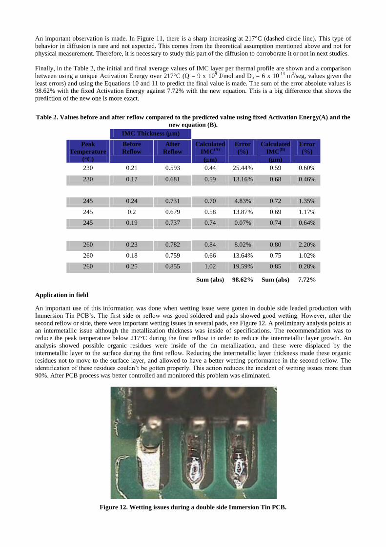
An important use of this information was done when wetting issue were gotten in double side leaded production with
Immersion Tin PCB’s. The first side or reflow was good soldered and pads showed good wetting. However, after the
second reflow or side, there were important wetting issues in several pads, see Figure 12. A preliminary analysis points at
an intermetallic issue although the metallization thickness was inside of specifications. The recommendation was to
reduce the peak temperature below 217°C during the first reflow in order to reduce the intermetallic layer growth. An
analysis showed possible organic residues were inside of the tin metallization, and these were displaced by the
intermetallic layer to the surface during the first reflow. Reducing the intermetallic layer thickness made these organic
residues not to move to the surface layer, and allowed to have a better wetting performance in the second reflow. The
identification of these residues couldn’t be gotten properly. This action reduces the incident of wetting issues more than
90%. After PCB process was better controlled and monitored this problem was eliminated.
Figure 12. Wetting issues during a double side Immersion Tin PCB.

Conclusions
The application of the XRF/CS Method has been very helpful to determine more acutely IMC layer growth or diffusion
in Immersion Tin PCB’s. This allows getting an important finding: there is also a linear relationship between the
activation energy and the IMC thickness. This was observed especially in temperature dynamic-state experiment with the
reflow profiles; although it is also applied to temperature steady-state experiments.
Another important finding is to see clearly the acceleration of the diffusion rate after a determined temperature in
Immersion Tin PCB’s. It was found the intermetallic formation was accelerated approximately at 217°C, very similar
temperature to the eutectic point of the copper-tin-silver. Because of that, the corroboration of Ag presence had to be
done with SEM/EDX analysis in the case of Immersion Tin pads. This phenomenon would also justify the fact of using
different Activation Energy Equation over 217°C. Applying a relationship between the Activation Energy and IMC
Thickness resulted in a linear equation with an approximate constant of 67680 J/mol for temperatures below 217°C and
32000 J/mol for temperatures over 217°C. This indicates the energy is to start the diffusion over 217°C is almost half that
of below 217°C.
The linear dependency between Q and IMC is positive; this means we will need more energy as long as the IMC growth.
This would be explained with the fact more energy would be needed to diffuse more atoms through a stable IMC layer,
this hypothesis needs to be proved. Although with the application of the new method to measure IMC layer and the
proposed set of equations is possible to simulate any thermal degradation of Immersion Tin, such as, passing PCB’s
through baking or several reflows, so quality issues can be prevented.
Acknowledgment
We wish to express my thanks to Pedro Juarez and Ivan Osorio, Process Coordinator and Plant EBS Manager, who
supported the project all the time.
References
1. Jennie S. Hwang, Environment-Friendly Electronics: Lead-Free Technology, (Electrochemical Publications,
2001), p. 422, 436-482.
2. John h. Lau, C.P. Wong, Ning Cheng Lee, S.W. Ricky Lee, Electronics Manufacturing with lead-free,
Halogen-Free, and Conductive-Adhesive Materials, McGraw-Hill Handbooks (2003).
3. Z. Zovac, and K.N. Tu, Immersion Tin: its chemistry, metallurgy, and application in electronic packaging
technology, IBM Journal Res. Develop. Vol 28 No. 6 November 1984 (1984).
4. K. Jung, and H. Conrad, Microstructure Coarsening during Static-Anneling of 60Sn40Pb Solder Joints: III
Intermetallic Compound Growth Kinetics, Journal of Electronic Material, Vol 30, No. 10 (2001).
5. N. C. Lee, Reflow soldering processes and troubleshooting: SMT, BGA, CSP, and flip chip technologies,
Newnes (2002).
6. Charles A. Harper, Electronic Material and Processes Handbook, Third Edition, McGraw Hill, (2004).
7. D.R. Askeland, P.P Fulay, W.J. Wrigth, the Science and Engineering of Materials, Cengage Learning, sixth
edition (2010).
8. Paul T. Vianco, Jerome A. Rejent, and Paul F. HLAVA, Solid-State Intermetallic Layer Growth Between Coppe
and 95.5Sn-3.9Ag-0.6Cu Solder, Journal of Electronic Material, Vol 33, No. 9 (2004).
9. J. Servin, New method to measure Intermetallic Compound Layer Thickness, Conference Proceeding, Materials
Science and Technology 2011 Conference and Exhibition, Columbus Ohio, USA (2011).
10. IPC – Association Connecting Electronics Industries. IPC-4554, Specification for Immersion Tin Plating,
January 2007.
11. Department of the Navy Science and Technology, The Benchmarking and Best Practices Center of Excellence,
The Lead Free Electronics Manhattan Project – Phase I , ACI Technologies, Inc. (2009).
12. Office of Pollution Prevention and Toxics, Office of Prevention, Pesticides, and Toxic Substances U.S.
Environmental Protection Agency, Technical Branch, National Program Chemicals Division, Methodology for
XRF Performance Characteristic Sheets, available on line at http://www.epa.gov/lead/pubs/r95-008.pdf (1997).
Last accessed on July 2010.
13. US Environmental Protection Agency, X-Ray Fluorescence (XRF) Instruments Frequently Asked Questions
(FAQ), 5/25/2004, available on line at http://www.epa.gov/superfund/lead/products/xrffaqs.pdf (2004). Last
accessed on July 2010.
14. US Department of Defense, Department of Defense Test Method, MIL STD I580 D, Destructive physical
analysis for Electronics, Electromagnetic, and Electromechanical Parts, 23 April 2010.
15. A. J. Bard, and L. R. Faulkener, Electrochemical Methods, Fundamentals and Applications, John Wiley & Sons,
Inc. 2nd Edition (2001).

16. C. Scheuerlein, G. A. Izquierdo, H. Charras, L. R. Oberli, and M. Taborelli, the thickness measurement of Sn-
Ag hot dip coatings on LHC superconducting strands by columetric, Large Hadron Collider Project, to be
published in the Journal of Electronic Society, November 2003.
17. D. Sewenson, the effects of suppressed beta tin nucleation on microstructural evolution of lead-free solder
joints, Lead-Free Electronic Solders, A Special Issue of the Journal of Materials Science: Materials in
Electronics, Springer Science+Business Media, LLC, 2007, p 39-54 (2007).
18. Minitab 16, Statistical and Process Management Software for Six Sigma and Quality Improvement, Help Files,
(2011).S
19. Sanka Ganesan and Michael Pecht, Lead-free Electronics, Wiley-Interscience, IEEE, (2006).
20. Matt Schaffer. Raymond A. Fournelle, and Jin Liang, Theory for Intermetallic Phase Growth Between Cu and
Liquid Sn-Pb Solder Based on Grain Boundary Difussion Control, Journal of Electronic Material, Vol 27, No.
10 (1999).
21. IPC –Association Connecting Electronics Industries and JEDEC, J-STD 020D, Moisture/Reflow Sensitivity
Classification for Nonhermetic Solid State Surface Mount Device , March 2008.
22. K.W. Moon, W.J. Boettinger, U.R. Kattner, F.S. Biancaniello, and C.A. Handwerker, Experimental and
Thermodynamic Assessment of Sn-Ag-Cu Solder Alloys, Journal of Electronic Material, Vol 30, No. 11 (2000).
23. NIST Material Measurement Laboratory, Phase Diagrams and Computational Thermodynamics, Ag-Cu-Sn
System, http://www.metallurgy.nist.gov/phase/solder/agcusn.html. Last accessed on July 2010.
24. Min-Hsien Lu and Ker-Chang Hsieh, Sn-Cu Intermetallic Grain Morphology to Sn Layer Thickness, Journal of
Electronic Material, Vol 36, No. 11 (2007).
25. A.S. Zuruzi, S.K. Lahiri, P. Burman, and K.S. Siow, Correlation Between Intermetallic Thickness and
Roughness During Solder Reflow, Journal of Electronic Material, Vol 30, No. 8 (2001).
26. Kang Jung and Hans Conrad, Microstructure Coarsening During Static Annealing on 60Sn40Pb Solder Joints: I
Stereology, Journal of Electronic Material, Vol 30, No. 10 (2001).
27. Kang Jung and Hans Conrad, Microstructure Coarsening During Static Annealing on 60Sn40Pb Solder Joints: II
Eutectic Coarsening Kinetics, Journal of Electronic Material, Vol 30, No. 10 (2001).