Metasurface Based Mid-infrared Devices
236
Metasurface Based Mid-infrared Devices Cheng Shi College of Engineering, Mathematics and Physical Science University of Exeter A thesis submitted for the degree of Doctor of Philosophy July 2019
Transcript of Metasurface Based Mid-infrared Devices
Metasurface Based Mid-infrared Devices
Cheng Shi
College of Engineering, Mathematics and Physical Science
University of Exeter
A thesis submitted for the degree of
Doctor of Philosophy
July 2019

Metasurface Based Mid-infrared Devices
Submitted by Cheng Shi to the University of Exeter
as a thesis for the degree of
Doctor of Philosophy in Engineering
In July 2019
This thesis is available for Library use on the understanding that it is copyright
material and that no quotation from the thesis may be published without proper
acknowledgement.
I certify that all material in this thesis which is not my own work has been identified
and that no material has previously been submitted and approved for the award of a
degree by this or any other University.
(Signature) …………………………………………………………………………………………
Cheng Shi
July 2019


Dedicated to Yiqi and Kaiwen


Acknowledgements
First of all, I would like to thank my supervisors, Prof Geoffrey Nash and Dr
Isaac Luxmoore, for their patient guidance and support during all my four years
of PhD study. Without their supervising, I doubt that I can be in this place today.
Geoff, you are always enthusiastic, knowledgeable and optimistic. Thank you
so much for giving me so many valuable advice both for academic research
and daily life, I knew if I get confused, you are always the right person I turn to
ask for guidance. Thank you also for taking so much for your valuable time in
reading this thesis and all the constructive comments. Isaac, you are always
more than willing to answer any questions I had, no matter how insignificant. I
benefited greatly from many fruitful discussions with you. I also appreciate your
efforts in getting me familiar with all the experiment equipment.
Next, I would also like to thank the colleagues in our group that I have
worked alongside these four years. Special thanks to Dr Nathan Mahlmeister
who fabricated the thermal emitters during the first years of my PhD. I’m also
grateful for the contributions of Dr Prarthana Gowda and Mr Callum Penrose,
Ms Jacqueline Pitts in the work of enhanced ATR spectroscopy. I also would
like to express my appreciate to Dr Tim Poole who gave me a lot of support and
suggestions in using the equipment in the cleaning room, and Ms Camilla
Owens who creates a lot of joy in the office, and all other supportive colleagues:

Dr Pouya Caroline, Dr Benjamin Ash, Ms Jessica Brown, Ms Vicky Kyrimi, Ms
Hannah Barnard, Ms Eleanor Osborne, and Ms Isabel Mitchell.
Outside my research group, I'd like to thank everyone in the CDT for all the
fun over the four years, especially to Laicong Deng, Carlota Ruiz De Galarreta,
Henry Fernandez, Ben Hogan, Joaquin Faneca. It is the friendships with you
that enrich my memory of the PhD life.
Last but not least, my deepest thanks to my family, my parents Liping Zhou
and Yaodong Shi. despite the long distance between Exeter and Shanghai, I
can always feel their encouragement, everlasting love and unconditional
financial and emotional support throughout the whole 4 years. Also greatest
appreciate with love to my wife, Yiqi Wang who stands by me through all my
travails and son, Kaiwen Shi. who brings a lot of joy into my life. They are the
intrinsic motivations for me to finish my degree.
Finally, I would like to say thank you to many other people whose names
are not mentioned here but this does not mean that I have forgotten their help.
1
ABSTRACT
The development of compact, efficient, and powerful mid-infrared devices is
mainly restrained by the limited choice of materials due to the high loss of
conventional optical materials in the mid-infrared range. The aim of this work
was to find alternative novel materials which would enable the realization of
devices with smaller size while maintaining its functionality. Metasurface and
graphene have emerged as promising materials which can help us to
manipulate the infrared light within nano-meter scale thickness. In this thesis,
three different mid-infrared devices, thermal emitter, wave trapping sensor and
phase modulator were designed based on either metasurface or both
metasurface and graphene. Devices were all fabricated with modern
semiconductor fabrication processes and their performances were also fully
investigated, both experimentally and through simulations.
A metasurface was first designed as a frequency selective layer on a
graphene thermal emitter to tailor the graybody emission spectrum from a
graphene filament into two discrete narrow bands for applications such as gas
sensing or molecule detection. The emission and reflectance spectra of the
devices were characterised using (FTIR) Fourier transform infrared
spectroscopy and showed good agreement with simulations based on the
Finite-difference time-domain (FDTD). method.
2
The use of a metasurface to enhance the interaction between molecular
vibrations and the evanescent waves, in a total attenuated reflectance system,
was also explored. A complementary ring-resonator structure was patterned
onto both silicon and SiO2/Si substrates, and the spectral properties of both
devices were characterised using an FTIR-ATR system. Experiments were
undertaken using 5µL mixtures containing trace amounts of butyl acetate
diluted with oleic acid. Without the use of a metasurface, the minimum
concentration of butyl acetate that could be clearly detected was 10%, whereas
the use of the metasurface on the SiO2/Si substrate allowed the detection of 1%
butyl acetate.
Finally, graphene was integrated into a metasurface structure to achieve
tunability of the design. The third device investigated was a phase modulator
which shows the capability to change the amplitude and phase of the reflected
wave by electrostatically gating the graphene from -90V to 90V. A dynamic
beam steering lens model which is made up of a unit cell consisting of four
phase modulator with different phase shift was also proposed to control the
angle for the reflected wave from specular to 30°.
i
Contents
List of Figures ....................................................................... i
List of Tables ........................................................................ i
List of Publications ............................................................... i
1 Introduction .................................................................. 1
Motivation ................................................................................... 1
Overview .................................................................................... 3
2 Fundamental Concepts and Background ................... 9
Introduction ................................................................................. 9
Gas detection ............................................................................. 11
Trace chemical detection ............................................................ 13
Infrared imaging and camouflage ................................................ 15
Metasurfaces ............................................................................ 18
Effective Medium Theory ............................................................ 21
Metasurface Applications ............................................................ 25
Graphene ................................................................................. 34
Electronic Properties ................................................................... 34
Thermal Properties ..................................................................... 42
3 Numerical Simulations ............................................... 48
Introduction ............................................................................... 48
ii
Solving Maxwell’s Equations .................................................... 49
Finite Element Method ................................................................ 50
FDTD method ............................................................................. 52
Simulation software and settings .............................................. 54
Simulation Software .................................................................... 54
Material Properties...................................................................... 56
Boundary Conditions .................................................................. 58
Mesh sizes ................................................................................. 60
Comparison between FEM and FDTD method ......................... 61
4 Device Fabrication ..................................................... 64
Introduction ............................................................................... 64
Metasurface fabrication ............................................................ 65
Electron beam lithography .......................................................... 65
Metallization ............................................................................... 68
2D-material fabrication ............................................................. 70
2D material transfer .................................................................... 70
Reactive ion etching ................................................................... 72
Fabricated Devices ................................................................... 74
5 Characterisation ......................................................... 75
Introduction ............................................................................... 75
iii
Metrology .................................................................................. 76
Optical Microscopy ..................................................................... 76
Scanning Electron Microscopy .................................................... 76
Atomic Force Microscopy............................................................ 79
Electromagnetic response characterization .............................. 82
Transmission Measurement ........................................................ 82
Reflection measurement ............................................................. 84
Emission measurement .............................................................. 87
Attenuated total reflection Measurement ..................................... 89
Conclusion ................................................................................ 92
6 Metamaterial-based Graphene Thermal Emitter ...... 93
6.1 Introduction ............................................................................... 93
6.2 Design ...................................................................................... 96
6.2.1 Single Band Emitter .................................................................... 96
6.2.2 Dual Band Emitter .................................................................... 102
6.3 Fabrication .............................................................................. 105
6.4 Reflection Measurement ......................................................... 109
6.5 Emission Measurement .......................................................... 114
6.6 Quality Factor Improvement ................................................... 118
6.7 Summary ................................................................................ 121
iv
7 Wave Trapping Sensor for Attenuated Total
Reflection Spectroscopy ..................................................... 123
Introduction ............................................................................. 123
Modelling ................................................................................ 127
Modelling of ATR configuration ................................................. 127
Modelling of the device ............................................................. 130
Fabrication and Measurement ................................................ 136
Device Fabrication and Measurement....................................... 136
Chemical Analytes Measurement ............................................. 140
Measurement of Chemical Analytes with metasurface devices . 143
8 Graphene-based Mid-infrared Modulator ............... 149
Introduction ............................................................................. 149
Design .................................................................................... 151
Experiment ............................................................................. 158
Application .............................................................................. 164
Summary ................................................................................ 168
9 Conclusions and Outlook ........................................ 170
Conclusions ............................................................................ 171
Metasurface-based Narrowband Graphene Thermal Emitter .... 171
Metasurface-enhanced ATR Spectroscopy ............................... 172

v
Graphene based metasurface phase modulator ....................... 173
Outlook ................................................................................... 174
Metasurface .............................................................................. 174
Graphene ................................................................................. 174
Bibliography ..................................................................... 176


List of Figures
i
List of Figures
Figure 1.1 The propagation loss for conventional semiconductor material in Infrared
wavelength range. Propagation loss more than 2 dB cm–1 is highlighted
in orange (illustration taken from Ref [17]). ........................................... 2
Figure 2.1 Absorption spectra for major natural greenhouse gases in the earth’s
atmosphere. From top to bottom: carbon monoxide, methane, nitrous
oxide, ozone, carbon dioxide, semiheavy water vapour, water vapour and
air (illustration taken from Ref. [42]). ................................................... 12
Figure 2.2 A thin, switchable thermal camouflage film covered on hand(illustrations
taken from Ref. [55]). .......................................................................... 17
Figure 2.3 Number of publications on metamaterials (a) and different applications (b)
of metamaterials between 2002 and 2012 (illustrations taken from Ref.
[92]). ................................................................................................... 19
Figure 2.4 Schematics of the definition of (a)Transfer Matrix and (b)S parameters. 23
Figure 2.5 (b) propagation phase, (c) permittivity and (d) permeability retrieved from
the negative refractive index metamaterial structure shown in (a)
(illustrations taken from Ref. [62]). ...................................................... 24
Figure 2.6 (a) Schematic diagram of a 3-layer cross-resonator absorber and absorption
spectra for (b) 1-layer cross structure; (c) 2-layer cross structure; (d) 3-
layer cross structure (illustrations from Ref [76]). ................................ 28
List of Figures
ii
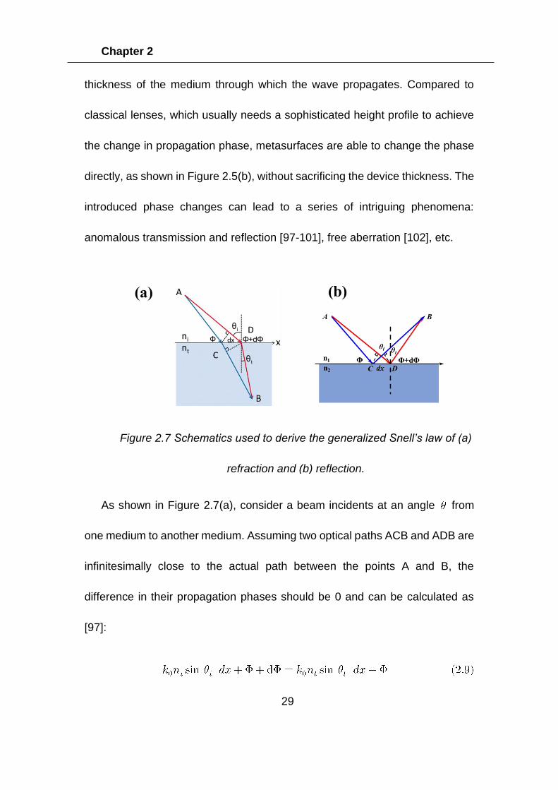
Figure 2.7 Schematics used to derive the generalized Snell’s law of (a) refraction and
(b) reflection. ...................................................................................... 29
Figure 2.8 (a) top: phase and amplitude profile required for the beam steering lens,
bottom: schematic of the resonator array for realizing the required phase
distribution and simulations of the scattered electric field for the individual
antennas composing the array (illustrations taken from [97]); (b) Flat
focusing lens with consisting of V-shaped nanoantenna array and the
transverse cross-section of its intensity profiles (illustrations taken from
[102]). ................................................................................................. 33
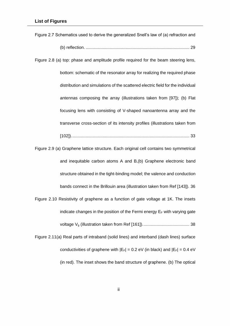
Figure 2.9 (a) Graphene lattice structure. Each original cell contains two symmetrical
and inequitable carbon atoms A and B,(b) Graphene electronic band
structure obtained in the tight-binding model; the valence and conduction
bands connect in the Brillouin area (illustration taken from Ref [143]). 36
Figure 2.10 Resistivity of graphene as a function of gate voltage at 1K. The insets
indicate changes in the position of the Fermi energy EF with varying gate
voltage Vg (illustration taken from Ref [161]). ...................................... 38
Figure 2.11(a) Real parts of intraband (solid lines) and interband (dash lines) surface
conductivities of graphene with |EF| = 0.2 eV (in black) and |EF| = 0.4 eV
(in red). The inset shows the band structure of graphene. (b) The optical
List of Figures
iii
response of moderately doped graphene in different spectral ranges
(illustrations from Ref [163])................................................................ 41
Figure 2.12 Phonon dispersion diagram of single-layer graphene along the Γ-to- M
crystallographic direction (illustration taken from Ref [136]). ............... 44
Figure 2.13 (a) Spatial images of the integrated infrared emission from graphene
channels with different gate voltage, (b) Corresponding I-V characteristic,
(c) Infrared intensity profile along the length of the graphene sample, (d)
More localized hotspot with bias graphene on a substrate with thinner
oxidized layer ((a-c) taken from Ref. [177], (d) taken from Ref. [178]). 47
Figure 3.1 Geometry for 2D and 3D meshes (elements) in COMSOL. .................... 51
Figure 3.2 (a) A graphical representation of a central-difference approximation to the
gradient at a point x0 (b). Illustration of a standard Cartesian Yee cell
used for FDTD which is composed of an electric cell and a magnetic cell
staggering in space (illustration taken from [188]). .............................. 53
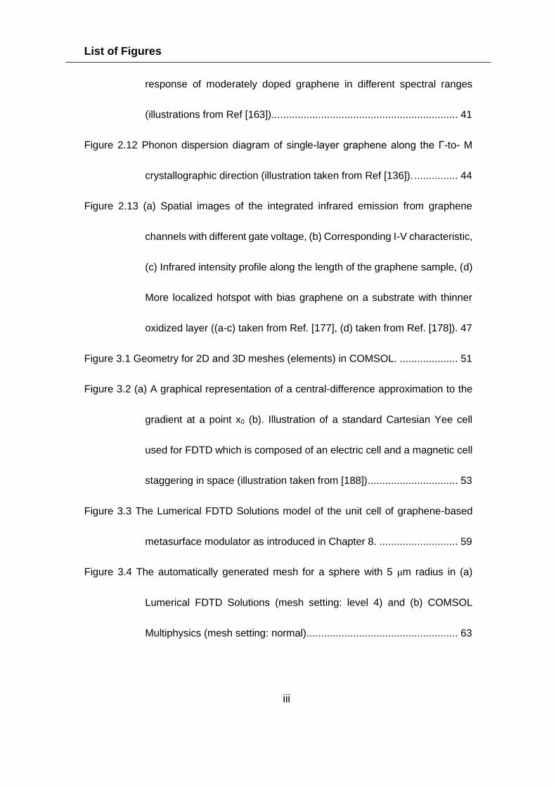
Figure 3.3 The Lumerical FDTD Solutions model of the unit cell of graphene-based
metasurface modulator as introduced in Chapter 8. ........................... 59
Figure 3.4 The automatically generated mesh for a sphere with 5 μm radius in (a)
Lumerical FDTD Solutions (mesh setting: level 4) and (b) COMSOL
Multiphysics (mesh setting: normal). ................................................... 63
List of Figures
iv
Figure 4.1 Schematic diagrams of the lithography processes on positive resist (top row)
or negative resist (bottom row). .......................................................... 66
Figure 4.2 Schematic diagram of metallization process on an EBL patterned sample.
........................................................................................................... 69
Figure 4.3 Schematic diagram of transferring of CVD 2D material grown on Cu foil to
a Si/SiO2 substrate. ............................................................................ 71
Figure 4.4 Schematic diagram of etching 2D material transferred on Si/SiO2 substrate.
........................................................................................................... 73
Figure 5.1 Schematic diagram of SEM working principle (illustration taken from [194]).
........................................................................................................... 78
Figure 5.2 Images of a split ring resonator structure proposed in Chapter 8 measured
under (a) optical microscope and (b) SEM by using a secondary electron
detector. ............................................................................................. 79
Figure 5.3 Schematic diagram of AFM working principle (illustration taken from [196]).
........................................................................................................... 81
Figure 5.4 (a)2D image and (b)3D image of ring resonators on an h-BN encapsulated
graphene filament. .............................................................................. 81
Figure 5.5 Schematic diagram and beam path of a Bruker Vertex 80v FTIR
spectroscopy (illustration taken from [198]). ....................................... 83
Figure 5.6 The external setup of FTIR spectroscopy for reflection measurement. ... 85
List of Figures
v
Figure 5.7 The external setup of FTIR spectroscopy for emission measurement. .... 87
Figure 5.8 (a) Bruker Platinum ATR module (illustration taken from [199]) (b)
Schematic diagram of the mechanism of ATR measurement. ............ 91
Figure 6.1 (a) 3D schematic and (b) top view of the unit cell of the design modelled in
the simulation. .................................................................................... 97
Figure 6.2 Simulated transmission (black line), reflection (red line) and absorption
spectrum of the unit cell of single annular ring resonator on the top of h-
BN encapsulated graphene thermal emitter. ....................................... 99
Figure 6.3 Cross sectional electric field distribution (colour plot) and surface current
(red arrows) in x-y plane between metasurface and substrate at λ = 4.4
µm. ................................................................................................... 100
Figure 6.4 (a) Simulated absorption/emission spectra of single annular ring resonator
unit cell with different radii ranges from 100 nm to 400 nm. (b) The
resonance wavelength of single annular ring resonator as a function of
radius of the annular ring resonator. ................................................. 101
Figure 6.5 (a) Top view and (b) simulated emission spectrum of double annular ring
resonator designs for dual band metasurface-based graphene thermal
emitter. ............................................................................................. 103
Figure 6.6 (a) Electric field and (b) surface current distributions in x-y plane between
the metasurface and substrate at 4.2 μm, (c) Electric field and (d) surface
List of Figures
vi
current distributions in x-y plane between the metasurface and substrate
at 6.6 μm .......................................................................................... 104
Figure 6.7 The cross section diagrams of fabricating the sample (i)-(vi): Formation of
the emission area. (vii)-(xii): Deposition of first and second contact on
outer edge. (xiii)-(xv) Transfer of top layer h-BN. (xvi)-(xix) Evaporation
of contact pads and metamaterial ring resonators. ........................... 107
Figure 6.8 (a) Top view of the schematic illustration of graphene narrowband thermal
emitter with quadrants. (b) Microscope image taken at 50× magnification
of the top of the emitter. (c) AFM image taken from within the red dash
box shown in (b). .............................................................................. 108
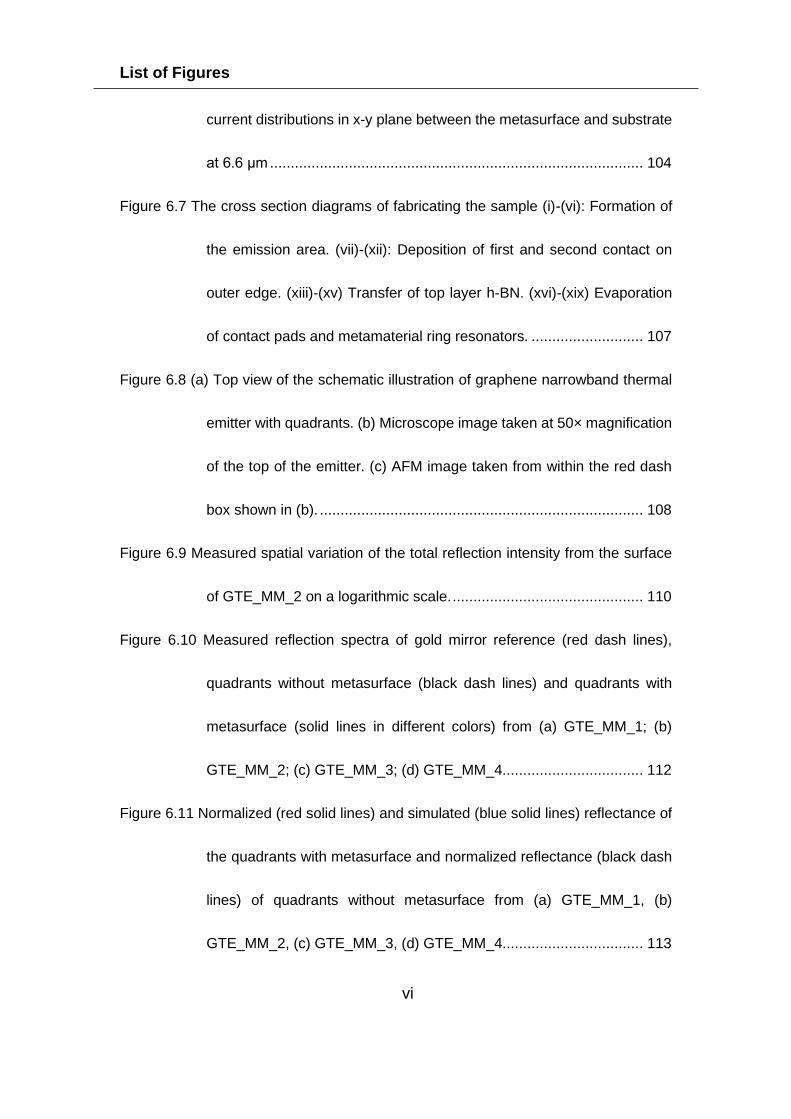
Figure 6.9 Measured spatial variation of the total reflection intensity from the surface
of GTE_MM_2 on a logarithmic scale. .............................................. 110
Figure 6.10 Measured reflection spectra of gold mirror reference (red dash lines),
quadrants without metasurface (black dash lines) and quadrants with
metasurface (solid lines in different colors) from (a) GTE_MM_1; (b)
GTE_MM_2; (c) GTE_MM_3; (d) GTE_MM_4.................................. 112
Figure 6.11 Normalized (red solid lines) and simulated (blue solid lines) reflectance of
the quadrants with metasurface and normalized reflectance (black dash
lines) of quadrants without metasurface from (a) GTE_MM_1, (b)
GTE_MM_2, (c) GTE_MM_3, (d) GTE_MM_4.................................. 113
List of Figures
vii
Figure 6.12 Measured spatial variation of the total emission intensity from the surface
of GTE_MM_2 on a logarithmic scale. .............................................. 115
Figure 6.13 Measured emission spectra of quadrants without metasurface (black dash
lines) and quadrants with metasurface (solid lines in different colors) from
(a) GTE_MM_1; (b) GTE_MM_2; (c) GTE_MM_3; (d) GTE_MM_4. . 116
Figure 6.14 Normalized (solid lines with different colors) and simulated (black solid
lines) emissivity of the quadrants with metasurface from (a) GTE_MM_1,
(b) GTE_MM_2, (c) GTE_MM_3, (d) GTE_MM_4. ........................... 117
Figure 6.15 (a) and (b) Emission spectra for substrates with different conductivities. (c)
Calculated radiation spectrum of the metamaterial-based graphene
thermal emitter on an aluminium substrate (blue line) based on the
measured radiation spectrum of a bare graphene thermal emitter (red
line). ................................................................................................. 119
Figure 6.16 Calculated Q-factors of both emission peaks (blue line for 1st emission
peak and red line for 2nd emission peak) for substrates with different
conductivities. ................................................................................... 120
Figure 7.1 (a) 3D schematic of the simulation model used to generate evanescent
wave with incident wave propagates along z-axis with an angle of
incidence θ and electric field polarized along x-axis. (b)The electric field
List of Figures
viii
distribution in x-z plane at k = 1000 cm-1 with incident angle = 10° (left)
and 45° (right). ................................................................................. 127
Figure 7.2 Reflectance obtained from the simulation model as a function of incident
angle. ............................................................................................... 129
Figure 7.3 (a) 3D perspective view and (b) top view with geometric parameters of the
device proposed for enhancing the sensitivity of ATR spectroscopy. 130
Figure 7.4 (a) Simulated reflectance spectra of the metasurface on Si substrate (b) and
(c) shows the electric field distribution for x-y plane at 450 cm-1 (dipole
mode) and 860 cm-1 (quadrupole mode). .......................................... 131
Figure 7.5 Simulated dispersion diagram of metasurface on Si/SiO2 substrate. The two
red dashed lines show the calculated resonance frequencies (dipole
mode and quadrupole mode) of uncoupled metasurface. The three black
dash lines represent frequencies of three surface optical phonon modes
in SiO2. The vertical white line represents the spectral response of the
metasurface on Si/SiO2 substrate presented in this paper. ............... 134
Figure 7.6 Comparison between the reflection spectra of metasurface on Si substrate
(black line) and on Si/SiO2 substrate (red line). ................................ 135
Figure 7.7 (a) the SEM photo of ATR-Si-M01; (b) measured reflectance spectra of
ATR-Si-M01 and ATR-SiO2-M01 under ATR configuration. .............. 138
List of Figures
ix
Figure 7.8 (a) Measured reflection spectra of metasurface with different scales on
Si/SiO2 substrate in the ambient atmosphere, spectra are consecutively
shifted by 0.25 vertically for clarity; (b) dispersion diagram as shown in
Figure 7.5 with extracted wavenumber of maxima and minima overlaid.
▼ and ▲ in blue, red and black corresponding to the maxima and
minima observed in the spectrum of ATR-SiO2-M03, ATR-SiO2-M01, and
ATR-SiO2-M02 respectively. ............................................................. 139
Figure 7.9 Measured absorption spectra of (a) 99.9% oleic acid and (b) 99.9% butyl
acetate. ............................................................................................ 140
Figure 7.10 Measured absorption spectra for mixtures in the ambient atmosphere,
spectra are consecutively shifted by 0.5 vertically for clarity; (b) Extinction
spectra for mixtures without the presence of metasurface. ............... 142
Figure 7.11 (a) Measured absorption spectra of mixtures in the presence of ATR-Si-
M01 in the ambient atmosphere, spectra are consecutively shifted by 0.2
vertically for clarity; (b) zoomed extinction spectra of mixtures in the
presence of ATR-Si-M01 for the carbon oxygen stretching band region
between 800 cm−1 and 1200 cm−1. ................................................... 144
Figure 7.12 (a) Measured absorption spectra of mixtures in the presence of ATR-SiO2-
M01 in the ambient atmosphere, spectra are consecutively shifted by 0.2
vertically for clarity; (b) zoomed extinction spectra of mixtures in the
List of Figures
x
presence of ATR-SiO2-M01 for the carbon–oxygen stretching band
region between 800 cm−1 and 1200 cm−1. ......................................... 146
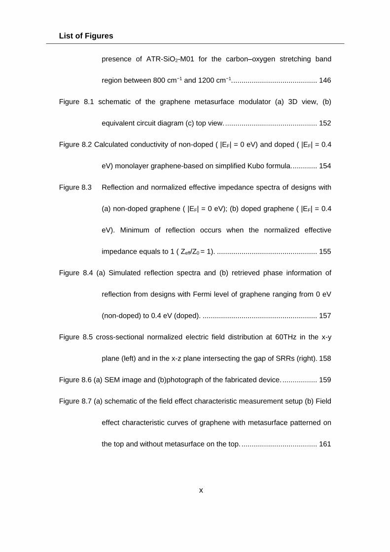
Figure 8.1 schematic of the graphene metasurface modulator (a) 3D view, (b)
equivalent circuit diagram (c) top view. ............................................. 152
Figure 8.2 Calculated conductivity of non-doped ( |EF| = 0 eV) and doped ( |EF| = 0.4
eV) monolayer graphene-based on simplified Kubo formula. ............ 154
Figure 8.3 Reflection and normalized effective impedance spectra of designs with
(a) non-doped graphene ( |EF| = 0 eV); (b) doped graphene ( |EF| = 0.4
eV). Minimum of reflection occurs when the normalized effective
impedance equals to 1 ( Zeff/Z0 = 1). ................................................. 155
Figure 8.4 (a) Simulated reflection spectra and (b) retrieved phase information of
reflection from designs with Fermi level of graphene ranging from 0 eV
(non-doped) to 0.4 eV (doped). ........................................................ 157
Figure 8.5 cross-sectional normalized electric field distribution at 60THz in the x-y
plane (left) and in the x-z plane intersecting the gap of SRRs (right). 158
Figure 8.6 (a) SEM image and (b)photograph of the fabricated device. ................. 159
Figure 8.7 (a) schematic of the field effect characteristic measurement setup (b) Field
effect characteristic curves of graphene with metasurface patterned on
the top and without metasurface on the top. ..................................... 161
List of Figures
xi
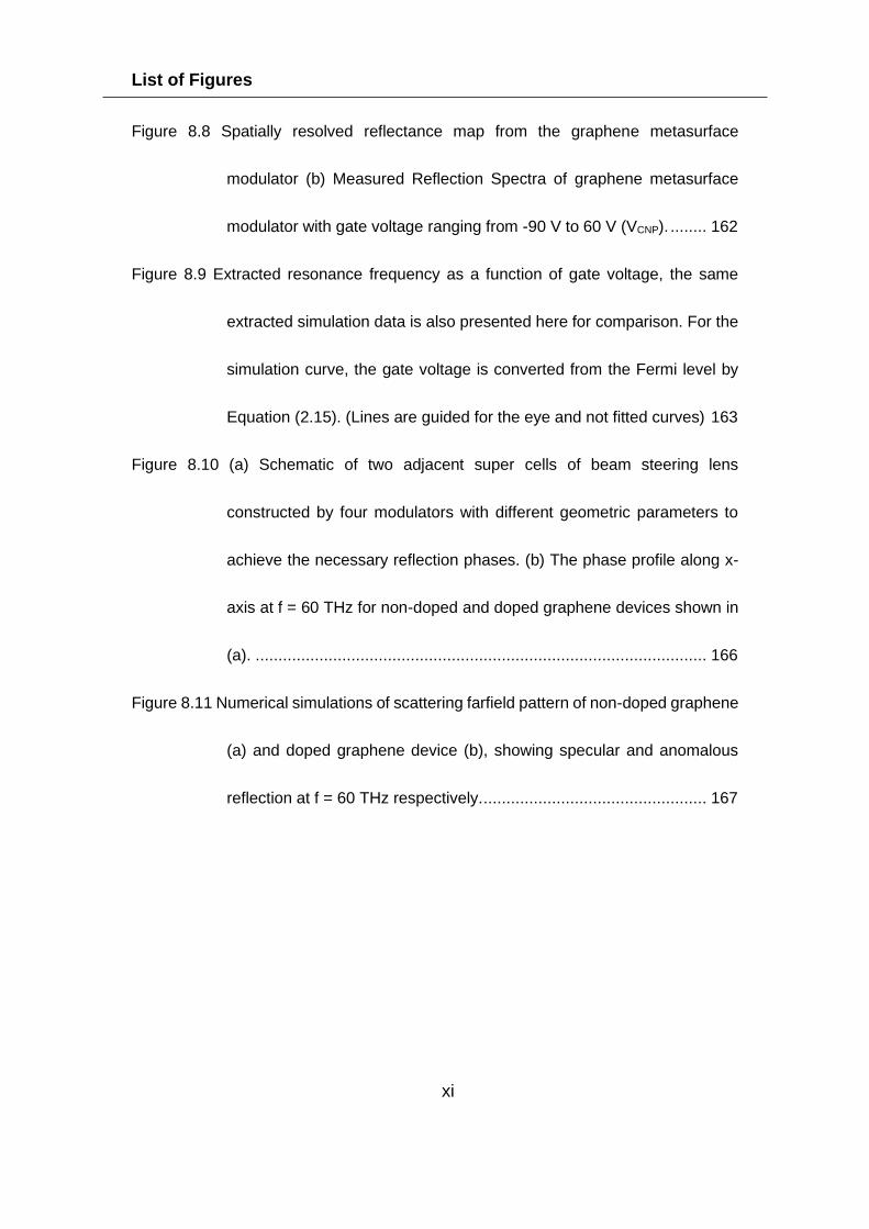
Figure 8.8 Spatially resolved reflectance map from the graphene metasurface
modulator (b) Measured Reflection Spectra of graphene metasurface
modulator with gate voltage ranging from -90 V to 60 V (VCNP). ........ 162
Figure 8.9 Extracted resonance frequency as a function of gate voltage, the same
extracted simulation data is also presented here for comparison. For the
simulation curve, the gate voltage is converted from the Fermi level by
Equation (2.15). (Lines are guided for the eye and not fitted curves) 163
Figure 8.10 (a) Schematic of two adjacent super cells of beam steering lens
constructed by four modulators with different geometric parameters to
achieve the necessary reflection phases. (b) The phase profile along x-
axis at f = 60 THz for non-doped and doped graphene devices shown in
(a). ................................................................................................... 166
Figure 8.11 Numerical simulations of scattering farfield pattern of non-doped graphene
(a) and doped graphene device (b), showing specular and anomalous
reflection at f = 60 THz respectively. ................................................. 167

List of Tables
i
List of Tables
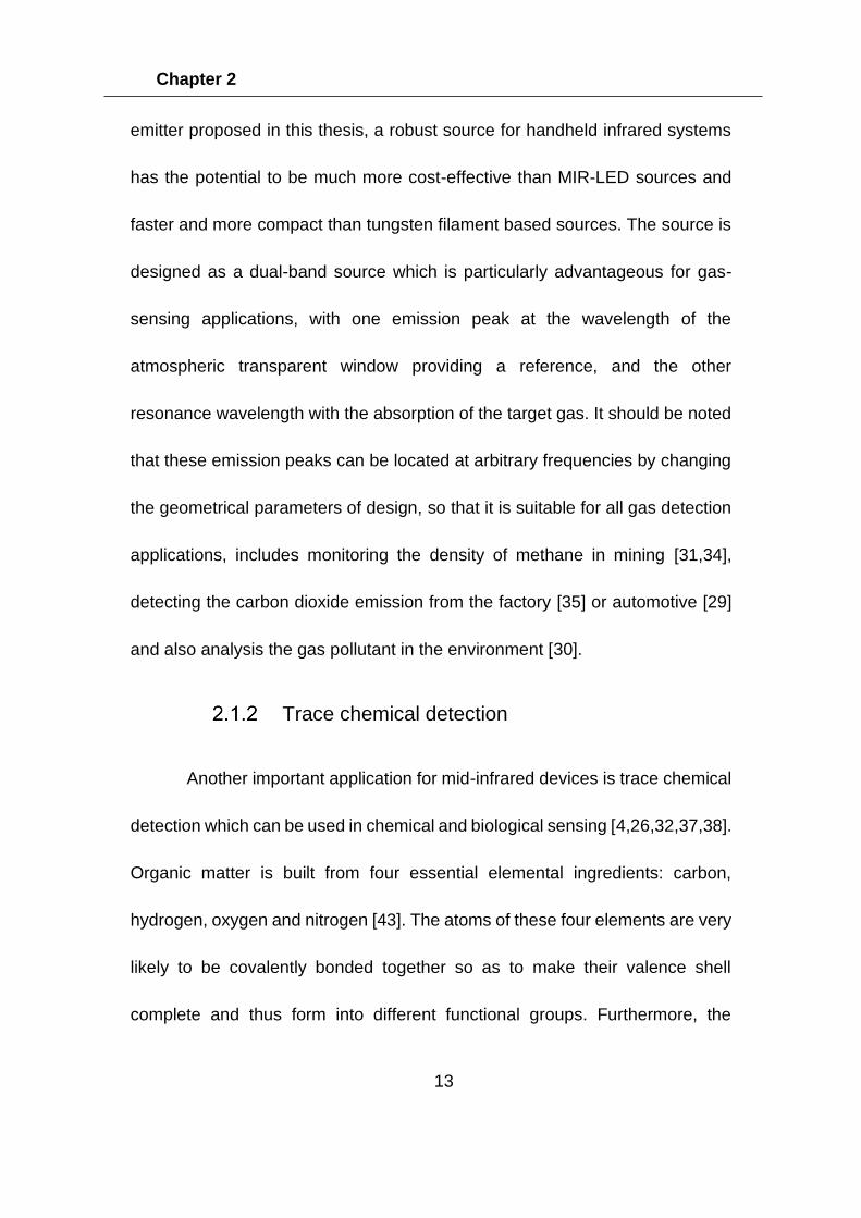
Table 2.1 Characteristic absorption frequencies of common organic functional groups.
(Ref [46]) ............................................................................................ 14
Table 4.1 List of fabricated devices characterized and discussed in this thesis ....... 74
Table 6.1 A list of double annular ring resonators based emitters with different
geometric parameters for fabrication and measurement. λ1 and λ2 are the
theoretical resonance wavelengths related to the large annular ring
resonators and small annular ring resonators. .................................. 105
Table 7.1 List of devices fabricated and measured in the experiment as well as their
geometric parameters....................................................................... 136
Table 8.1 Geometric parameters of modulators used in beam steering lens ......... 166

List of Publications
i
List of Publications
[1] Shi, C., Luxmoore, I. J., & Nash, G. R. Gate tunable graphene-integrated
metasurface modulator for mid-infrared beam steering. Optics Express
27, 14577-14584 (2019).
[2] Shi, C., Luxmoore, I. J., & Nash, G. R. Graphene-based Metamaterial
Tunable Phase Modulator for Mid-Infrared Wave Steering. In CLEO2019
JTh2A-26 (2019).
[3] Shi, C., Penrose, C., Pitts, J. E., Gowda, P., Luxmoore, I. J., & Nash, G.
R. Metamaterial-enhanced infrared attenuated total reflection
spectroscopy. Nanoscale Advances, 1, 476-480 (2019).
[4] Shi, C., Mahlmeister, N.H., Luxmoore, I.J. and Nash, G.R., Metamaterial-
based graphene thermal emitter. Nano Research 11, 3567-3573 (2018).
[5] Shi, C., Zang, X. F., Ji, X. B., Chen, L., Cai, B., Nash, G. R., & Zhu, Y. M.
Compact broadband terahertz perfect absorber based on multi-
interference and diffraction effects. IEEE Transactions on. Terahertz
Science and Technologies 6, 40–44 (2016).

Chapter 1
1
1 Introduction
Motivation
The mid-infrared (MIR) spectral region of 2-20 μm contains strong
characteristic vibrational transitions of many important molecules [1,2] as
well as two atmospheric transmission windows between 3-5 μm and 8-13
μm [3], which makes it crucial for applications in spectroscopy [4-7],
materials processing [8], chemical and bio-molecular sensing [9,10],
security and industry [11]. Although there is a huge variety of potential
applications in the mid-infrared regime, research on efficient MIR functional
devices still remains challenging [12]. First of all, with the development of
infrared industries, more sensitive and cost-effective devices are required
for precise measurements. In addition, the idea of making infrared systems
portable or handheld so that people can use those systems doing
measurement and analysis directly on-site attracts increasing research
interest [13-15]. This requires the components in the system to be designed
as compact and integrable, but to remain cost-effective and feasible for
fabrication. It is already not a trivial thing to fulfil only the latter two
requirements simultaneously, let alone taking addition consideration of
Chapter 1
2
portability and reliability into the design. Besides, mid-infrared devices are
restrained by a limited choice of conventional optical elements. Although
optical glass is widely used in fabricating optical devices as it can achieve
nearly 100% transparency in optical wave band, its high transmission is
limited to the wavelength less than 3.5 µm due to the vibrational modes
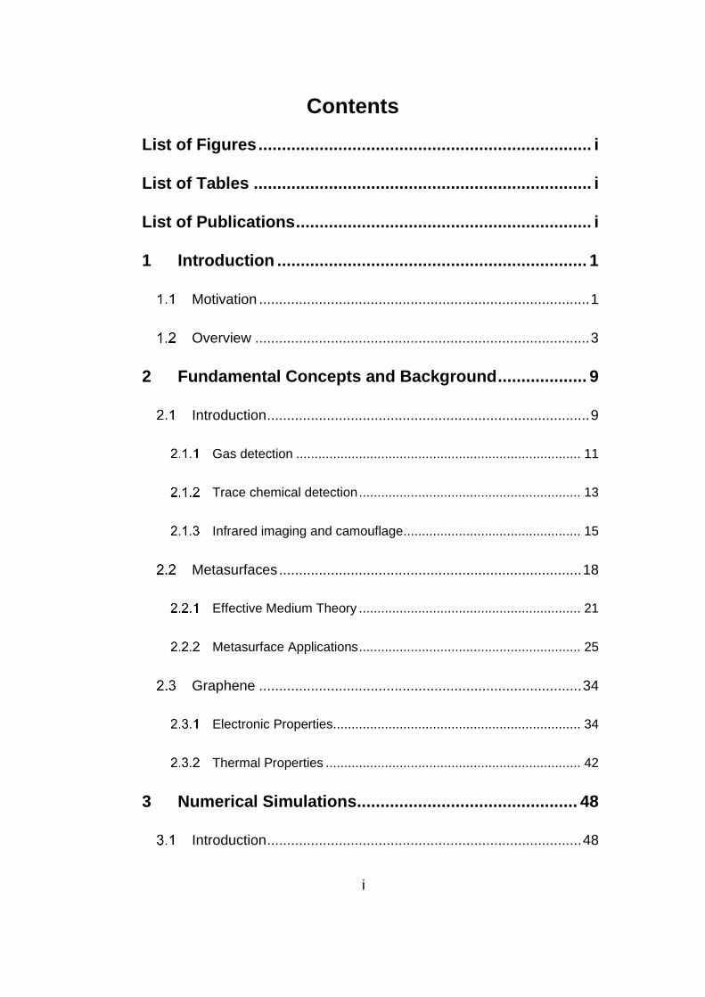
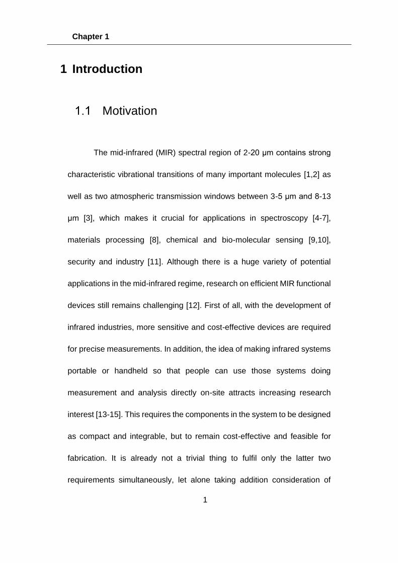
associated with oxygen [16]. As shown in Figure 1.1, most of Group III or
Group IV compounds have their cutoff frequencies in the mid-infrared
regime. Although silicon and germanium have a relatively wide range of
transmission window in the mid-infrared band, the energy propagated
through these materials will be reduced by more than 50% due to their high
refractive indices (nSi = 3.7, nGe = 4.05) [17]. Besides, other chemical
compounds like calcium fluoride (CaF2), potassium bromide (KBr), barium
Figure 1.1 The propagation loss for conventional semiconductor material in
Infrared wavelength range. Propagation loss more than 2 dB cm–1 is
highlighted in orange (illustration taken from Ref [17]).
Chapter 1
3
fluoride (BaF2) have a broad transmission window as well as a high
transmittance [18], but their softness and crystalline solid-state structures
made it extremely difficult to be patterned on the surface, and are thus
difficult to use in the fabrication of certain devices.
As a highly significant breakthrough, metasurfaces have been
developed as promising building blocks in designing optoelectronic devices,
by delicately engineering parameters or materials of those individual
building blocks and selecting specific design algorithms. Furthermore,
when integrating 2D materials like graphene into the metasurface, even
more exceptional applications can be realized like thermal management,
modulation, etc. Metasurface-based devices are promising to replace their
conventional opponents due to their better performance and compact size.
Overview
The main results presented in this thesis are the study on the design,
fabrication, and characterization of three different metasurface-based
devices in the mid-infrared regime. The first device is an h-BN/graphene
encapsulated incandescent mid-infrared emitter with metasurface structure
integrated on the top. The second device is designed to enhance the
Chapter 1
4
measurement sensitivity of attenuated total reflection (ATR) mid-infrared
spectroscopy. The third device demonstrated is the active mid-infrared
reflective modulator, whose performance can be tuned by changing the
gate voltage applied on the device. Performances of all three devices are
simulated and optimized by utilizing commercial software, Lumerical FDTD
Solutions, which is based on finite difference time domain (FDTD) method
and COMSOL Multiphysics, which is on the basis of finite element method
(FEM). Devices were then fabricated in an ISO Class 5 cleanroom by
following a set of delicate processes, followed by testing via a powerful
Fourier Transform Infrared (FTIR) Spectroscopy. The measurement results,
which are in good agreement to the simulation results, demonstrate the
potential applications of those metasurface based mid-infrared devices in
areas such as gas sensing, trace chemical detection, and thermal imaging.
The rest of this thesis is structured as follows:
Chapter 2 gives background information on metasurfaces and
graphene, two key elements in our device designs. The first section
introduces some common strategies to design metasurfaces at the desired
frequency, including details on the effective medium theory, as well as
using this theory to design metasurface for perfect absorbers and ultrathin
lenses. This is followed by a discussion on one of the most promising 2D
Chapter 1
5
materials, graphene. Information on both electrical and thermal properties
of graphene will be covered.
Chapter 3 presents details on two main simulation methods, the
FEM and the FDTD method, which we applied to simulate the response of
our devices presented in this thesis. Introduction to each method, and their
settings for material properties, mesh sizes and boundary conditions are
also discussed in this chapter.
Chapter 4 provides descriptions of the methodology involved in the
fabrication of the devices presented in the thesis. The chapter will start with
background information on the fabrication process of a metasurface
structure on a substrate, including electron beam lithography, and thermal
evaporation. This introduction is followed by the descriptions on the transfer
the transfer process of chemical vapour deposition (CVD) 2D materials like
graphene and hexagonal boron nitride (h-BN) to various substrates along
with the patterning process by using reactive ion etching machine.
Chapter 5 introduces different kinds of set-ups of the Fourier
transform infrared spectroscopy measurement systems used in the
experiments, covering transmission (characterization for substrate),
reflection (characterization for active reflective modulator), emission
Chapter 1
6
(characterization for metasurface-based graphene thermal emitter), ATR
(characterization for chemicals and wave trapping sensor for chemical
detection),with background information of on the Bruker FTIR spectroscopy
provided.
Chapter 6 investigates how the metasurface layer applied as a
frequency selective surface (FSS) to tailor the thermal radiation spectrum
from multilayer graphene infrared emitters. It was observed that CVD
multilayer graphene can be thought of like a classic filament bulb with
uniform channel resistance, but could be driven with much higher frequency,
up to 100 kHz [19]. In order to obtain a narrowband emission spectrum, a
metasurface structure is integrated into the CVD multilayer graphene
infrared emitter. By comparing the measured spatial variations and spectra
of the thermal emission from both patterned and unpatterned multilayer
graphene infrared emitter, distinct differences can be noticed. The
possibility of increasing the quality factor (Q factor) by integrating another
metallic back-reflector layer is also investigated. An adapted form of this
part of the chapter was published in Nano Research 11, (2018) [20].
Chapter 7 begins with a full detailed introduction on our COMSOL
model which is built to simulate the condition of an ATR setup. Research
Chapter 1
7
on enhancing the detection of trace chemicals in a commercial attenuated
total reflection setup is also demonstrated in this chapter. An array of
periodic subwavelength metallic complimentary ring resonators patterned
as metasurface layer on different substrates are investigated to improve
the sensitivity of FTIR-ATR measurement. Geometric parameters of the
metasurface structure are designed to ensure the resonance frequency of
metasurface overlapping one of the vibrational modes of the analytes. This
overlap will result in a strong interaction between the electromagnetic wave
confined in the air gap and chemical analytes trapped there. An even
stronger interaction is observed for an oxidized silicon substrate, due to the
aforementioned two resonance modes coupling into the phonon mode of
SiO2. More details can be referred to our publication in the associated
journal, Nanoscale Advances, 1 (2019) [21].
Chapter 8 shows our design on combining the metasurface
structure and graphene as a whole active reflective modulator in the mid-
infrared regime. Graphene, well known for its unique gapless bandstructure,
introduces a wide range of tunable conductivity to the device for
modulation. 300 nm thick SiO2 on an aluminium covered Si substrate is
used in device fabrication so that the graphene conductivity can be
directly controlled by the gate voltage applied on the aluminium layer.
Chapter 1
8
Preliminary results show a 150° modulation in phase can be achieved at
60THz by altering the gate voltage from -90V to 90V. In the second
section, we show the application of a beam-steering lens by constructing
four such modulators but with different geometric parameters as a new
unit cell. Due to a 0 to 2π phase variation over the unit cell will be
established as soon as the gate voltage is applied, our simulation results
show that the biased device will reflect the beam with an extra 30°
compared to when the device is unbiased. Parts of the results presented in
this chapter have been published in CLEO proceedings 2019 [22] and
Optics Express, 27 (2019) [23].
Chapter 9 summarizes the results presented in this thesis in
addition to provides outlooks on the future development of metasurfaces
and graphene.
Chapter 2
9
2 Fundamental Concepts and Background
Introduction
In this chapter, we introduce three main applications of mid-infrared light:
gas sensing, chemical detection, and thermal imaging. However, these
applications are hindered by the relatively poor performance of mid-infrared
optoelectronic devices which suffers from slowing responding time, poor
sensitivities, and lack of flexibility. Thus, not only powerful but also compact and
improved devices are required to promote the development of the infrared
industry. However, advances in material sciences are opening up new routes
to achieve this goal. Among these materials, metasurfaces and graphene are
essential building blocks of the devices explored in this research due to their
unique properties and ultrathin thicknesses. Metasurfaces, the planar form of
metamaterials, which can be regarded as a homogeneous layer with artificial
electromagnetic properties will be introduced in Section 2.2. Electromagnetic
properties like permittivity and permeability can be precisely extracted with the
assistance of effective medium theory, which will be described in detail in §
2.2.1. The retrieved values are crucial for the design and analysis of the
metasurface devices. In § 2.2.2, research on two applications based on
Chapter 2
10
metasurfaces, perfect absorbers and ultrathin flat lenses will be reviewed to
show how infrared light can be controlled by such a thin layer of structures. In
Section 2.3, the electronic and thermal properties of graphene will be discussed.
Due to the high carrier mobility of graphene and the fact that graphene can be
easily doped by electrons and holes through electrostatic gating or chemical
doping, the graphene-integrated device’s response to the electromagnetic
wave could be directly controlled by the doping level of graphene within a
response time less than 1 ns [24], which is a great breakthrough for applications
like modulators.
Most of the objects around us are composed of nothing but molecules
which in turn are formed by atoms linked together through either covalent
bonding or ionic bonding [25]. If we regard the bonding as a massless spring,
the atoms vibrate along with the spring and rotating around the axis. When light
is incident on a substance, the radiation is transmitted, reflected or absorbed in
varying degrees, depending upon the substance and the wavelength of the
radiation [26]. At the atomic and molecular level, when a molecule is excited by
a photon, the energy of the photon is absorbed by the molecule. Each molecule
can vibrate and rotate in certain patterns, and for each pattern, there is an
associated amount of energy of motion [10]. A molecule can only absorb energy
from a photon if the energy matches precisely such an energy state of that
Chapter 2
11
molecule. Notably, the frequencies of these energy states are mostly located in
the mid-infrared band, particularly in 2-8 μm [27] which is one of the reasons
why the mid-infrared range has attracted so many research interests. For the
last two decades, mid-infrared devices have been widely used in a commercial
infrared system for such applications as environment monitoring [28-30,35],
organic matter analysis [36], medical diagnostics [37,38], and thermal imaging
[39-41], etc.
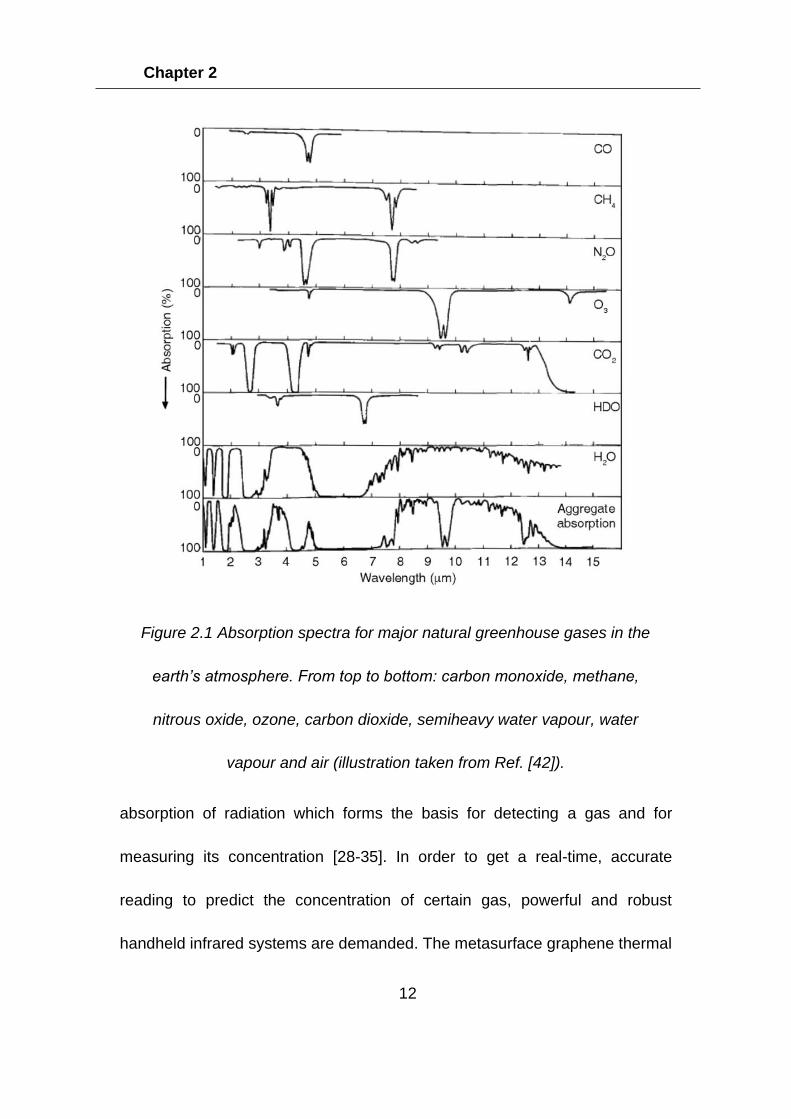
Gas detection
For many gases, there are a large number of photon energies in the
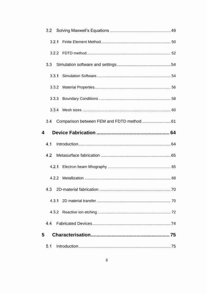
mid-infrared range that can be absorbed by gas molecules: As depicted in
Figure 2.1, each gas exhibits a very specific set of absorption wavelengths
which depend on the strength of the chemical bonds between the atoms that
make up the molecule. Unlike diatomic molecules composed of like atoms such
as oxygen (O2), hydrogen (H2), chlorine (Cl2), and nitrogen (N2) or infrared
transparent inert gases (He, Ne, Ar, Kr, Xe, Rn) which oscillate at shorter
wavelength such as ultraviolet and X-rays, greenhouse gas molecules like
carbon dioxide (CO2), nitrogen dioxide (NO2) or methane (CH4) exhibit
oscillation modes that match the energy of mid-infrared radiation. The
oscillation modes might be stretching and bending motions. It is this selective
Chapter 2
12
absorption of radiation which forms the basis for detecting a gas and for
measuring its concentration [28-35]. In order to get a real-time, accurate
reading to predict the concentration of certain gas, powerful and robust
handheld infrared systems are demanded. The metasurface graphene thermal
Figure 2.1 Absorption spectra for major natural greenhouse gases in the
earth’s atmosphere. From top to bottom: carbon monoxide, methane,
nitrous oxide, ozone, carbon dioxide, semiheavy water vapour, water
vapour and air (illustration taken from Ref. [42]).
Chapter 2
13
emitter proposed in this thesis, a robust source for handheld infrared systems
has the potential to be much more cost-effective than MIR-LED sources and
faster and more compact than tungsten filament based sources. The source is
designed as a dual-band source which is particularly advantageous for gas-
sensing applications, with one emission peak at the wavelength of the
atmospheric transparent window providing a reference, and the other
resonance wavelength with the absorption of the target gas. It should be noted
that these emission peaks can be located at arbitrary frequencies by changing
the geometrical parameters of design, so that it is suitable for all gas detection
applications, includes monitoring the density of methane in mining [31,34],
detecting the carbon dioxide emission from the factory [35] or automotive [29]
and also analysis the gas pollutant in the environment [30].
Trace chemical detection
Another important application for mid-infrared devices is trace chemical
detection which can be used in chemical and biological sensing [4,26,32,37,38].
Organic matter is built from four essential elemental ingredients: carbon,
hydrogen, oxygen and nitrogen [43]. The atoms of these four elements are very
likely to be covalently bonded together so as to make their valence shell
complete and thus form into different functional groups. Furthermore, the
Chapter 2
14
carbon atom can form long chains, known as carbon skeleton, which connect
different carbon-based functional group and build up more complicated organic
compounds. Researchers have successfully identified the absorption peaks for
hundreds of organic compound in the mid-infrared regime in the past several
decades [44,45], they also found that some functional groups absorb infrared
radiation at about the same wavelength. For instance, as demonstrated in Table
2.1, there are three similar hydrogen stretching groups, alkanes (-C-H),
carboxylic acids (-O-H) and amines (-N-H). Alkane stretching vibrations
Table 2.1 Characteristic absorption frequencies of common organic
functional groups. (Ref [46])
Chapter 2
15
usually appear between 3200 and 2800cm-1, carboxylic acids stretching
vibrations occur between 3650 and 3600cm-1, and amines stretching vibrations
locate between 3500 and 3300cm-1. These types of infrared bands are called
group frequencies because they tell us about the presence or absence of
specific functional groups in a sample [45]. However, quantifying the
concentration of those chemicals are far more difficult than qualifying them as
the sensitivity of the most advanced spectroscopy techniques is limited by the
weak light-matter interaction caused by the size mismatch between molecules
and the wavelength. The second device presented in this thesis, a metasurface
sensor based on wave trapping, was used to demonstrate an improvement of
ten-fold in trace chemical detection. This is potentially extremely important for
studies of biological samples, including proteins, lipids, carbohydrates, and
nucleic acids, where usually only a small amount of samples can be obtained
for the study.
Infrared imaging and camouflage
Apart from the unique interaction with molecules, the infrared band is
also widely used in imaging, especially when the visible condition is poor. Unlike
light can easily be blocked by smoke and light fog, the infrared light is able to
successfully penetrate through them. Thus infrared vision is used extensively
Chapter 2
16
for night vision [47,48], navigation [49], surveillance [50,51] and rescue [52].
With advancements in infrared detection technology, there is also a growing
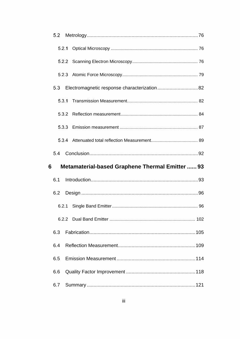
need for infrared countermeasures like infrared camouflage [53-56]. Although
during the past few years, the concept of invisibility [57-59] and illusion [60,61]
has already been proposed and proven in microwave band on the basis of
transformation optics and conformal mapping, it is impracticable to scale down
those designs to make them function in the mid-infrared regime due to the
challenge of fabricating such small features. Traditional thermal camouflage
uses a low-emissivity coating, which reduces the object’s apparent radiation
temperature, to make the object blend into the background [53,54]. However,
the emissivity of a traditional camouflage coating is fixed, and the objects can
only be camouflaged in a fixed background temperature. Once the background
temperature changes, the object can be easily detected by thermal imaging
cameras because of the difference in radiation temperature between the object
and the background. Realizing an effective adaptive thermal camouflage is not
trivial as it requires a material that can adapt to different temperatures, and with
an extremely fast response time. Some of the drawbacks limited the
development of thermal camouflage so far include poor thermal fluctuation,
slow response times, and the requirement for rigid materials, to name a few.
Recent progress has been reported by O. Salihoglu et al which relies on electro-
Chapter 2
17
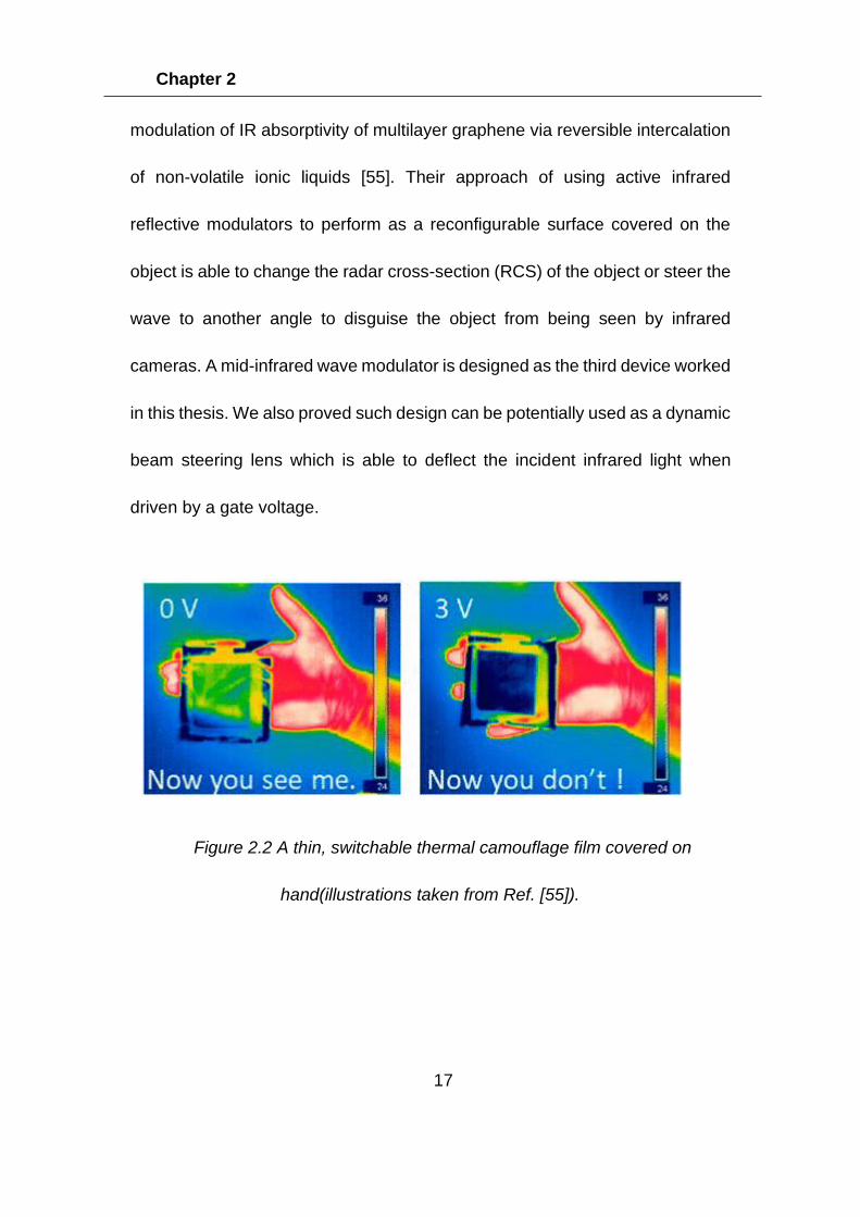
modulation of IR absorptivity of multilayer graphene via reversible intercalation
of non-volatile ionic liquids [55]. Their approach of using active infrared
reflective modulators to perform as a reconfigurable surface covered on the
object is able to change the radar cross-section (RCS) of the object or steer the
wave to another angle to disguise the object from being seen by infrared
cameras. A mid-infrared wave modulator is designed as the third device worked
in this thesis. We also proved such design can be potentially used as a dynamic
beam steering lens which is able to deflect the incident infrared light when
driven by a gate voltage.
Figure 2.2 A thin, switchable thermal camouflage film covered on
hand(illustrations taken from Ref. [55]).
Chapter 2
18
Metasurfaces
The advent of metamaterials opens a new era for designing electromagnetic
wave devices. Metamaterials are usually constructed by periodic unit cells,
whose size and spacing are much smaller than the wavelengths of incoming
electromagnetic radiation. Consequently, the electromagnetic wave does not
experience the microscopic details of each unit cells, but treat it as a
homogenous medium [62-65]. Thus engineering the nanostructure of
metamaterials is equivalent to artificially design atoms to achieve
electromagnetic properties that are not available or not easily obtainable in
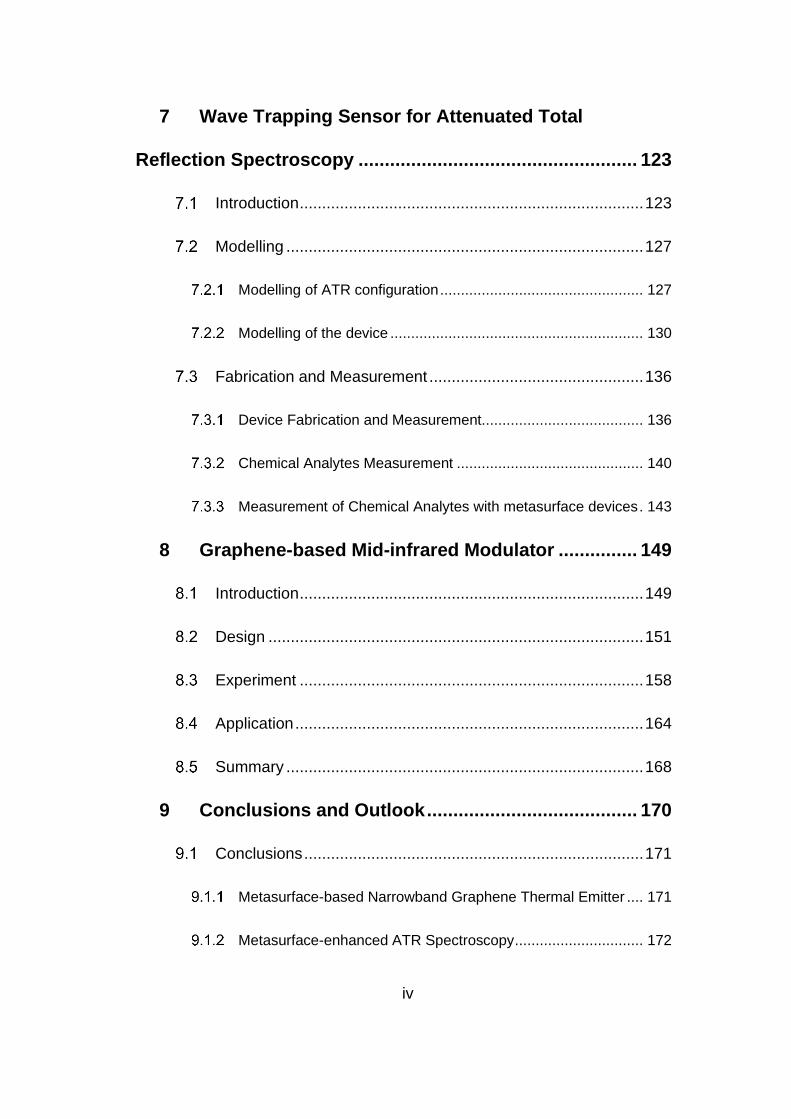
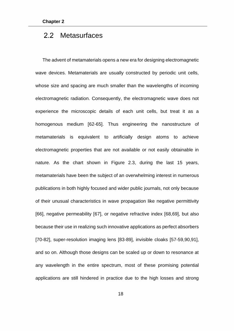
nature. As the chart shown in Figure 2.3, during the last 15 years,
metamaterials have been the subject of an overwhelming interest in numerous
publications in both highly focused and wider public journals, not only because
of their unusual characteristics in wave propagation like negative permittivity
[66], negative permeability [67], or negative refractive index [68,69], but also
because their use in realizing such innovative applications as perfect absorbers
[70-82], super-resolution imaging lens [83-89], invisible cloaks [57-59,90,91],
and so on. Although those designs can be scaled up or down to resonance at
any wavelength in the entire spectrum, most of these promising potential
applications are still hindered in practice due to the high losses and strong
Chapter 2
19
Figure 2.3 Number of publications on metamaterials (a) and different
applications (b) of metamaterials between 2002 and 2012 (illustrations
taken from Ref. [92]).
Chapter 2
20
dispersion associated with the resonant responses and the use of metallic
structures. In addition, whereas metamaterial-based devices can be easily
fabricated for the microwave band, where the size of the features is in millimetre
scale, it remains a huge challenge for realizing the required 3D structures in
sub-micrometre scale, i.e. designs for infrared range or optical range. These
two main obstacles of metamaterials drove many metamaterial researchers to
focus on a single layer of planar structures, which were later termed as
metasurfaces, that can be readily fabricated using existing technologies such
as lithography and nanoimprinting methods. Meanwhile, the ultrathin thickness
along the wave propagation direction can greatly reduce the unnecessary
losses caused by the structure [93]. In general, metasurfaces can overcome
the problems associated with metamaterials, while their interactions with
incident waves can be still strong enough to provide very useful functionalities
[94-96]. Over the past decade, metasurfaces have attracted great attention and
have been proved to have the potential to replace 3D metamaterials in many
applications in mid-infrared region, such as perfect absorbers [68-70,79,80],
ultrathin lenses [97-103], holograms [104-106]. The metasurface can also be
designed to enhance the electric field to improve the interaction between
electromagnetic fields and objects [107,108], which is beneficial for applications
Chapter 2
21
in mid-infrared band such as imaging, sensing, photovoltaics, and photo-
emission [109–113].
Effective Medium Theory
Smith et al. first applied this practical method to assign bulk material
properties to inhomogeneous metamaterials [62]. Suppose a beam of
electromagnetic wave is propagating from one side of a metamaterial layer to
the other. Assuming that the metamaterials perform like a homogenous medium
with refractive index and relative impedance , the relation between the
input electromagnetic field and the output electromagnetic field can be defined
by the transfer matrix method as
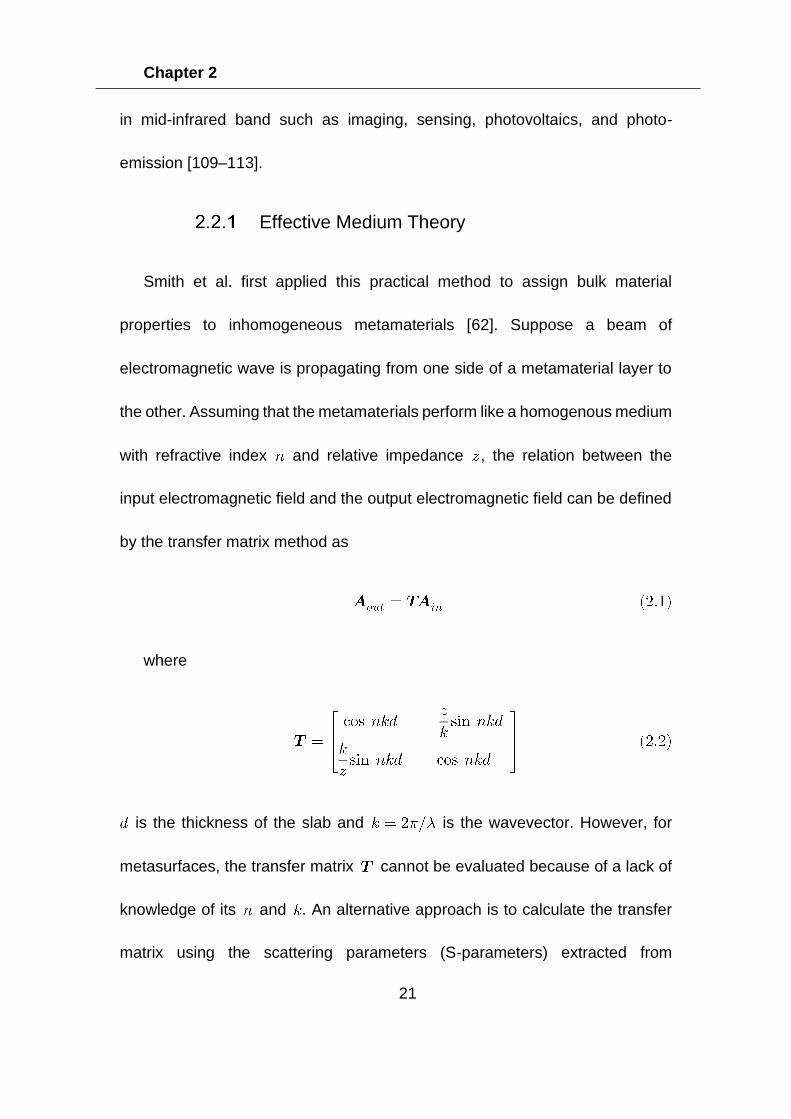
where
is the thickness of the slab and is the wavevector. However, for
metasurfaces, the transfer matrix cannot be evaluated because of a lack of
knowledge of its and . An alternative approach is to calculate the transfer
matrix using the scattering parameters (S-parameters) extracted from
Chapter 2
22
simulations. The S-parameters, as shown in Figure 2.4, link the incoming field
amplitudes to the outgoing field amplitudes and can also be directly related to
experimentally determined quantities. The elements of the transfer matrix can
be expressed by the values of S-parameters as follows:
Because the medium is assumed to be homogenous, so that we can get
and , the equations can be simplified into:
Using the analytic expression for the T-matrix elements in Equation (2.2) gives
the refractive index and relative wave impedance of the effective medium
in terms of S-parameters:
Chapter 2
23
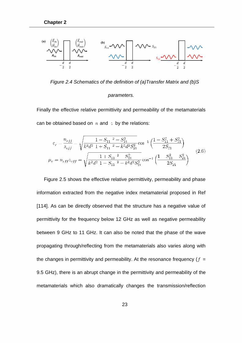
Finally the effective relative permittivity and permeability of the metamaterials
can be obtained based on and by the relations:
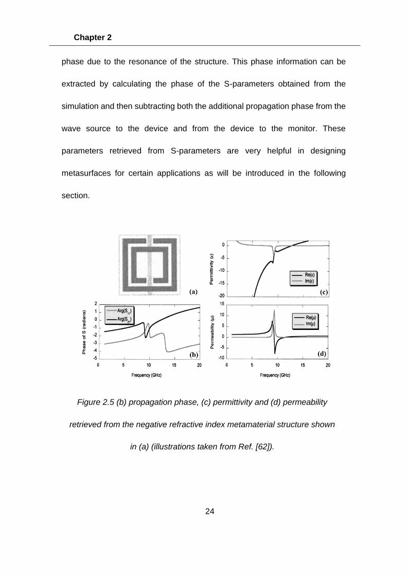
Figure 2.5 shows the effective relative permittivity, permeability and phase
information extracted from the negative index metamaterial proposed in Ref
[114]. As can be directly observed that the structure has a negative value of
permittivity for the frequency below 12 GHz as well as negative permeability
between 9 GHz to 11 GHz. It can also be noted that the phase of the wave
propagating through/reflecting from the metamaterials also varies along with
the changes in permittivity and permeability. At the resonance frequency ( =
9.5 GHz), there is an abrupt change in the permittivity and permeability of the
metamaterials which also dramatically changes the transmission/reflection
Figure 2.4 Schematics of the definition of (a)Transfer Matrix and (b)S
parameters.
Chapter 2
24
phase due to the resonance of the structure. This phase information can be
extracted by calculating the phase of the S-parameters obtained from the
simulation and then subtracting both the additional propagation phase from the
wave source to the device and from the device to the monitor. These
parameters retrieved from S-parameters are very helpful in designing
metasurfaces for certain applications as will be introduced in the following
section.
Figure 2.5 (b) propagation phase, (c) permittivity and (d) permeability
retrieved from the negative refractive index metamaterial structure shown
in (a) (illustrations taken from Ref. [62]).
Chapter 2
25
Metasurface Applications
i) Metasurface absorbers
Metamaterial perfect absorbers, are one of the first metamaterial-based
devices being realized for practical applications. High absorption is desired in
many applications, such as energy harvesting [115,116], scattering reduction
[117], as well as thermal sensing [118]. Near-unity absorption can be achieved
by the use of a metallic ground plane to block all the wave propagating through
the device while eliminating the entire reflection at the interface. According to
the Fresnel formula of reflection, when a beam of wave incidents from air to a
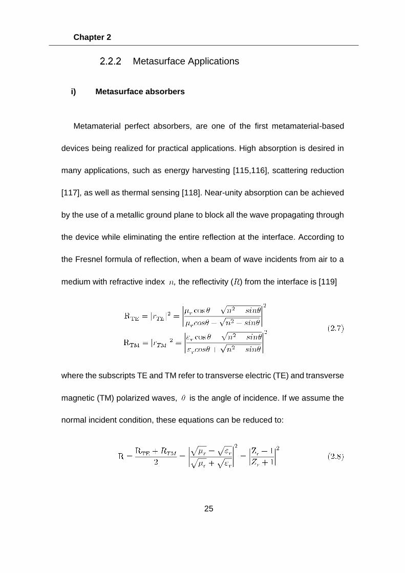
medium with refractive index , the reflectivity ( ) from the interface is [119]
where the subscripts TE and TM refer to transverse electric (TE) and transverse
magnetic (TM) polarized waves, is the angle of incidence. If we assume the
normal incident condition, these equations can be reduced to:
Chapter 2
26
where is the relative wave impedance. For classical
electromagnetic absorbers, the permittivity and permeability of conventional
materials won’t support the reduction in reflection at the interface. Thus the
approach adopted by those absorbers is to design a resonant cavity as an anti-
reflection layer, for example, the design of Salisbury screens which consists of
a thin resistive layer and a metal ground plane separated by a dielectric spacer
of quarter wavelength thickness. In that case, the wave directly reflected from
the interface will destructively interfere with the wave reflected through one
round-trip propagation path and lead to the reduction in total reflection at a
certain wavelength. However, the design is bulky and only can absorb energy
over a narrow bandwidth. The mainstream design of metasurface absorbers
inherits the three-layer Salisbury screen configuration, but replaces the top
resistive layer by a metasurface. As mentioned in the effective medium theory,
the metasurface can be treated as a homogenous layer with an effective
relative permittivity and permeability. Research has shown that the effective
relative permittivity of the metasurface is due to the electrical resonant response
of individual elements in the metallic structure of the metasurface, and the
effective relative permeability is attributed to the magnetic resonance resulting
from anti-parallel surface currents between the top metasurfaces element and
the ground plane [72,92]. The metasurface can thus be regarded as a
Chapter 2
27
frequency selective surface (FSS) because it can fulfil the wave impedance
matching condition, 1, to eliminate the reflection at the artificial
frequency by tailoring both and independently through adjusting the
geometric dimensions of the metasurface structures and the thickness of the
spacer layer. In comparison to the conventional absorbers, the thickness of
metasurface absorbers can be dramatically reduced because the dielectric
spacer layer not necessarily needs to be as thick as a quarter of the wavelength.
Although for most metasurface designs, the bandwidth for unity absorption is
also narrow, broadband absorption can be achieved by stacking several layers
of metasurface resonating at close resonance frequencies [73,74,76] or using
lossy material like heavily doped silicon as the spacer layer [77-80]. Figure
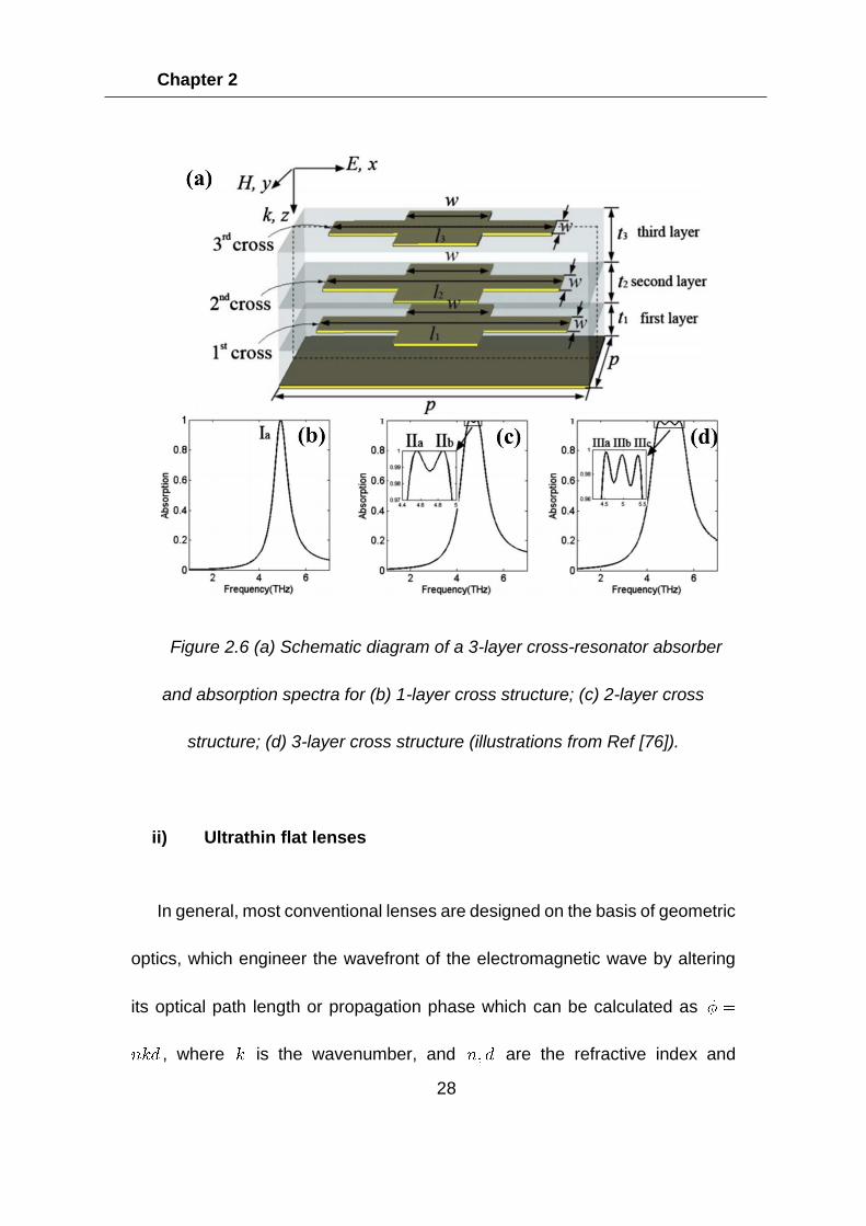
2.6(a) illustrates a metamaterial absorber structure consisting of three layers of
cross-resonators with appropriate geometric dimensions and spacer
thicknesses. The three resonance frequencies in close proximity merge
together and form a broader absorption bandwidth as shown in Figure 2.6(b-d).
Other metasurface-based absorbers have also been proposed and
experimentally tested for more novel functionalities such as multi-band
absorbers [81,82], coherent absorbers [121,122], frequency tunable absorbers
[123,124].
Chapter 2
28
ii) Ultrathin flat lenses
In general, most conventional lenses are designed on the basis of geometric
optics, which engineer the wavefront of the electromagnetic wave by altering
its optical path length or propagation phase which can be calculated as
, where is the wavenumber, and are the refractive index and
Figure 2.6 (a) Schematic diagram of a 3-layer cross-resonator absorber
and absorption spectra for (b) 1-layer cross structure; (c) 2-layer cross
structure; (d) 3-layer cross structure (illustrations from Ref [76]).
Chapter 2
29
thickness of the medium through which the wave propagates. Compared to
classical lenses, which usually needs a sophisticated height profile to achieve
the change in propagation phase, metasurfaces are able to change the phase
directly, as shown in Figure 2.5(b), without sacrificing the device thickness. The
introduced phase changes can lead to a series of intriguing phenomena:
anomalous transmission and reflection [97-101], free aberration [102], etc.
As shown in Figure 2.7(a), consider a beam incidents at an angle from
one medium to another medium. Assuming two optical paths ACB and ADB are
infinitesimally close to the actual path between the points A and B, the
difference in their propagation phases should be 0 and can be calculated as
[97]:
Figure 2.7 Schematics used to derive the generalized Snell’s law of (a)
refraction and (b) reflection.
Chapter 2
30
where is the wave number in air, is the refractive index of the
medium where the wave coming from, is the distance between the two
cross points C and D, and are the phases at these two points, and
is the refraction angle. Similarly, for the reflection shown in Figure 2.7(b), we
have:
when there is no abrupt phase change along the surface ( = 0), Equations
(2.9) & (2.10) will lead to the classical Snell’s law:
However, if a phase discontinuity is introduced to this interface, Snell’s law in
Equation (2.11) will be generalized to:
The anomalous refraction and reflection angles can thus be derived from
Equation (2.12). For normal incidence in air, those two angles can be calculated
as:
Chapter 2
31
the key challenge in using metasurfaces is therefore to fully control the
wavefront lies in designing metasurface structures that can cover the whole 0
to 2 phase range. In some of the pioneering work on metasurfaces, V-shaped
nanoantennas were proposed and experimentally demonstrated by Yu et al to
control the propagation of linearly polarized light in the mid-infrared range
[97,125]. The research was then extended to the optical [98], near-infrared (NIR)
[100], and terahertz [101] range. However, since there is no theoretical relation
between the metasurface design and the phase shift, a series of time-
consuming simulations that sweep through one or more geometric parameters
of the design have to be ran to test all the possible phase shift values the design
can achieve. As a simpler method for designing metasurface for circularly
polarized (CF) wave, Huang et al proposed a metasurface based on gold
nanorods to manipulate the phase profile by employing Pancharatnam–Berry
(PB) phase [98]. The beauty of this approach lies in the linear dependence of
phase delay on the orientation angle of each nanorod, i.e., , with
the sign determined by the polarity of the incident wave, which saves huge
efforts in simulations. Other designs like Huygen’s metasurfaces [126,127],
Chapter 2
32
multilayer metasurfaces [128,129], etc are also proved to be able to cover the
2 phase range.
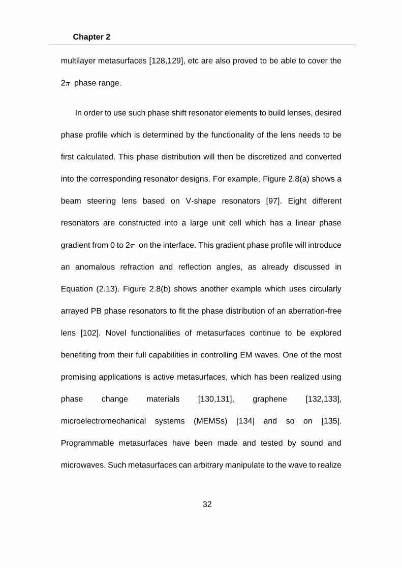
In order to use such phase shift resonator elements to build lenses, desired
phase profile which is determined by the functionality of the lens needs to be
first calculated. This phase distribution will then be discretized and converted
into the corresponding resonator designs. For example, Figure 2.8(a) shows a
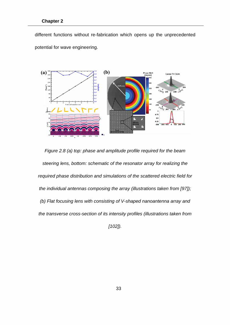
beam steering lens based on V-shape resonators [97]. Eight different
resonators are constructed into a large unit cell which has a linear phase
gradient from 0 to 2 on the interface. This gradient phase profile will introduce
an anomalous refraction and reflection angles, as already discussed in
Equation (2.13). Figure 2.8(b) shows another example which uses circularly
arrayed PB phase resonators to fit the phase distribution of an aberration-free
lens [102]. Novel functionalities of metasurfaces continue to be explored
benefiting from their full capabilities in controlling EM waves. One of the most
promising applications is active metasurfaces, which has been realized using
phase change materials [130,131], graphene [132,133],
microelectromechanical systems (MEMSs) [134] and so on [135].
Programmable metasurfaces have been made and tested by sound and
microwaves. Such metasurfaces can arbitrary manipulate to the wave to realize
Chapter 2
33
different functions without re-fabrication which opens up the unprecedented
potential for wave engineering.
Figure 2.8 (a) top: phase and amplitude profile required for the beam
steering lens, bottom: schematic of the resonator array for realizing the
required phase distribution and simulations of the scattered electric field for
the individual antennas composing the array (illustrations taken from [97]);
(b) Flat focusing lens with consisting of V-shaped nanoantenna array and
the transverse cross-section of its intensity profiles (illustrations taken from
[102]).
Chapter 2
34
Graphene
Apart from metasurfaces, graphene opens up another new possibility to
manipulate mid-infrared light within an atomic-thick layer. This monolayer of
carbon atoms arranged in a 2D honeycomb lattice has attracted interest due to
its extraordinary thermal [136-138], mechanical [139,140] and electrical
properties [141-143] since first being isolated in 2004. Through the studies in
the past decade, both the understanding of graphene properties and the
improved fabrication methods producing large scale high-quality graphene
have paved the path for the development of graphene-based devices which can
manipulate electromagnetic waves in the mid-infrared regime. In the following
two sections, we will mainly focus on the thermal and electrical properties of the
graphene in order to explore how to take advantage of these intriguing
properties into the design of mid-infrared devices.
Electronic Properties
Due to the hexagonal structure of graphene, 3 out of 4 electrons in the
outer shell of each carbon atom forms strong covalent σ bonds with
neighbouring carbon atoms within the sheet, while the 4th electron is located in
the pz orbital out of the plane. For monolayer graphene, these free electrons
Chapter 2
35
link up together and form the bonds which determine the exceptional
electronic properties of graphene. The linear dispersion relation is the most
discussed and unprecedented one among all those extraordinary properties. It
can be proved, with the assistance of the tight-binding model [144] that, the
dispersion relation between kinetic energy and wavenumber is linear for
monolayer graphene and can be expressed as , where is Planck
constant and = 1.1×10⁶ m/s is the Fermi velocity for graphene. Because
the Fermi velocity is approaching the speed of light, the electrons in graphene
are no longer non-relativistic particles and cannot be described by Schrödinger
equation any more. Instead, they should be regarded as Dirac fermions with
negligible effective mass and follow the Dirac equation [145]. This leads to a
number of novel physical phenomena for monolayer graphene, such as an
unconventional quantization sequence in the quantum Hall regime [146, 147],
Klein tunnelling [148,149] and Veselago lensing [150].
Furthermore, based on this dispersion relation, the band structure of
monolayer graphene can be calculated. As plotted in Figure 2.9, it can be
clearly observed that in the band structure, there is no gap between the valence
and the conduction bands as these two bands touch each other at a number of
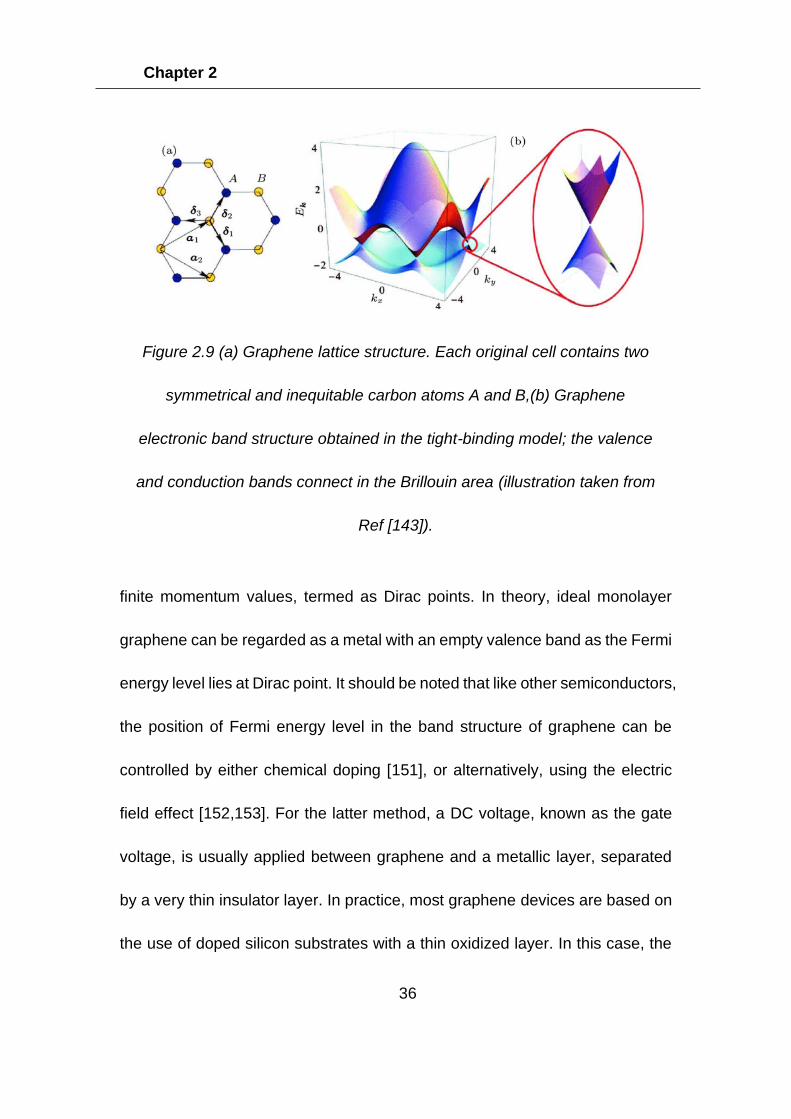
Chapter 2
36
finite momentum values, termed as Dirac points. In theory, ideal monolayer
graphene can be regarded as a metal with an empty valence band as the Fermi
energy level lies at Dirac point. It should be noted that like other semiconductors,
the position of Fermi energy level in the band structure of graphene can be
controlled by either chemical doping [151], or alternatively, using the electric
field effect [152,153]. For the latter method, a DC voltage, known as the gate
voltage, is usually applied between graphene and a metallic layer, separated
by a very thin insulator layer. In practice, most graphene devices are based on
the use of doped silicon substrates with a thin oxidized layer. In this case, the
Figure 2.9 (a) Graphene lattice structure. Each original cell contains two
symmetrical and inequitable carbon atoms A and B,(b) Graphene
electronic band structure obtained in the tight-binding model; the valence
and conduction bands connect in the Brillouin area (illustration taken from
Ref [143]).
Chapter 2
37
silicon is one plate of a capacitor, the SiO2 is the dielectric, and graphene is the
other plate. The surface charge density introduced into the graphene can
be calculated as:
where = 8.854×10⁻¹² F/m is the permittivity in free space, is the electron
charge, are the thickness and permittivity of the thin dielectric layer. The
variation in the carrier density will shift the Fermi energy level of graphene as
follow:
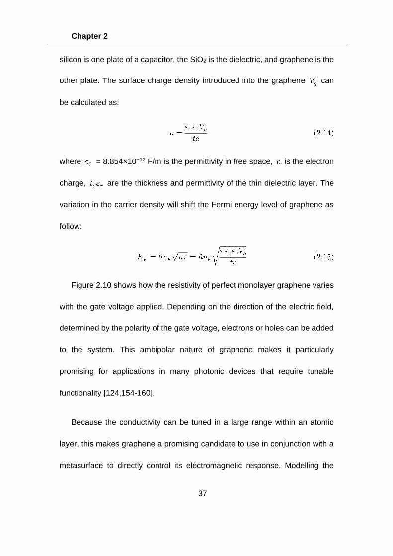
Figure 2.10 shows how the resistivity of perfect monolayer graphene varies
with the gate voltage applied. Depending on the direction of the electric field,
determined by the polarity of the gate voltage, electrons or holes can be added
to the system. This ambipolar nature of graphene makes it particularly
promising for applications in many photonic devices that require tunable
functionality [124,154-160].
Because the conductivity can be tuned in a large range within an atomic
layer, this makes graphene a promising candidate to use in conjunction with a
metasurface to directly control its electromagnetic response. Modelling the
Chapter 2
38
conductivity of the graphene is thus of paramount importance in designing
active optoelectronic devices. The conductivity of monolayer graphene can be
modelled with the assistance of the Kubo formula, a quantum transport
theoretical framework. Assuming the graphene sheet is in the x-y plane, its
extended non-local anisotropic model for conductivity should follow the tensor
form [159]:
Figure 2.10 Resistivity of graphene as a function of gate voltage at 1K. The
insets indicate changes in the position of the Fermi energy EF with varying
gate voltage Vg (illustration taken from Ref [161]).
Chapter 2
39
in which are the conductivity tensor along and
directions. Noting that and , equation (2.16) can be
rewritten as:
where are the conductivities along diagonal and off-diagonal
directions, and are the symmetric and antisymmetric dyads. The general
expressions for of monolayer graphene, derived from the Kubo
formalism [162], are:
and
where is the energy of nth Landau level and
is its Fermi-Dirac distribution, is the excitonic
Chapter 2
40
band gap, are the charge of an electron, Boltzman constant and
reduced Planck constant. = 1.1×10⁶m/s, as mentioned earlier, is the Fermi
velocity of graphene, and is the chemical potential, the same as Fermi
energy level, and is dependent on the external electric field for doping.
is the external magnetic field applied TO the graphene, and is the intrinsic
scattering rate of graphene. Both diagonal and off-diagonal conductivities are
very complicated and cannot be evaluated analytically. In this thesis, we
assume both the magnetic bias field and the excitonic band gap are negligible.
In this case, the off-diagonal conductivity term will vanish as , and the
graphene can thus be regarded as isotropic. This will also simplify equation the
to an approximation expression [159]:
As can be observed from Equation (2.20), the final expression of graphene
conductivity model is the sum of two terms. The first term accounts for the
carrier transitions within the same band, known as intraband transitions, while
the second term stands for interband transitions, transitions between different
bands.
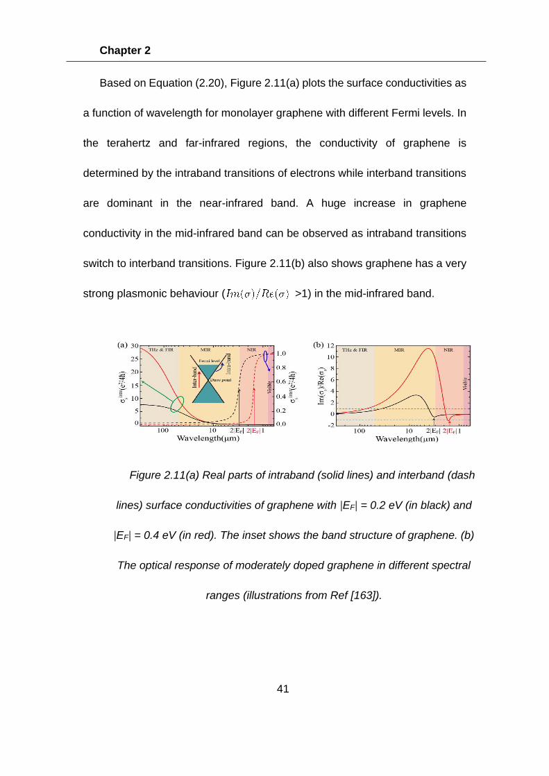
Chapter 2
41
Based on Equation (2.20), Figure 2.11(a) plots the surface conductivities as
a function of wavelength for monolayer graphene with different Fermi levels. In
the terahertz and far-infrared regions, the conductivity of graphene is
determined by the intraband transitions of electrons while interband transitions
are dominant in the near-infrared band. A huge increase in graphene
conductivity in the mid-infrared band can be observed as intraband transitions
switch to interband transitions. Figure 2.11(b) also shows graphene has a very
strong plasmonic behaviour ( >1) in the mid-infrared band.
Figure 2.11(a) Real parts of intraband (solid lines) and interband (dash
lines) surface conductivities of graphene with |EF| = 0.2 eV (in black) and
|EF| = 0.4 eV (in red). The inset shows the band structure of graphene. (b)
The optical response of moderately doped graphene in different spectral
ranges (illustrations from Ref [163]).
Chapter 2
42
These features, together with the high carrier mobility opens up a new era
of plasmon research. Compared to the noble metal plasmon, graphene
plasmon exhibits stronger energy confinement [158,164-166] and tunability
[153,160]. Those two prominent properties can help to achieve the
enhancement of light-matter interaction in a tiny area at a controllable frequency,
which is ideal for selective sensing. Over the past 5 years, graphene
nanoribbons have been intensively studied in the terahertz and mid-infrared
regions to excite localized plasmon for detecting polar phonons of the substrate
[160,167,168], molecular vibrations of adsorbates [151,164,166], and lattice
vibrations of other atomically thin layers [169]. However, monolayer graphene
can only achieve at most 2.3% absorption which limits its modulation depth. In
order to reach the full potential of graphene plasmons. A metasurface can be
used in conjunction with graphene to achieve a deeper modulation width
[157,170].
Thermal Properties
Thermal conductivity is usually used to describe a material’s ability to
transfer heat. In solid materials, heat is generally carried by electrons or through
vibrations of atoms, known as phonons. As a result, the thermal conductivity
can be calculated as , where and are the phonon and
Chapter 2
43
electron contribution, respectively. For heavily doped semiconductors or metals,
electrons are the main heat carriers due to the large concentration of free
charges in those materials. can be thus evaluated by the conductivity of
the material via Wiedemann-Franz Law [171]
where = 1.602×10⁻¹⁹ C is the charge of an electron, = 1.38×10⁻²³ J/K is
the Boltzmann’s constant and is the temperature of the material. However
for non-metallic materials, is dominant in thermal conductivities. This is
even applicable to some materials like graphite [160] or graphene which also
have high electrical conductivity because of their strong covalent sp2 bonding
as introduced in the last section. The phonon distribution can be
calculation as the summation of each phonon mode [172]:
where is the thickness of the material, is the phonon energy of the
th phonon mode at wave vector , is the Bose-
Einstein phonon equilibrium distribution function. are the group
velocity and relaxation time of the phonon from th branch. For graphene, its
hexagonal lattice leads to the formation of six phonon modes ( = 6), three
optical (O) and three acoustic (A) phonon modes [136]. Like other materials,
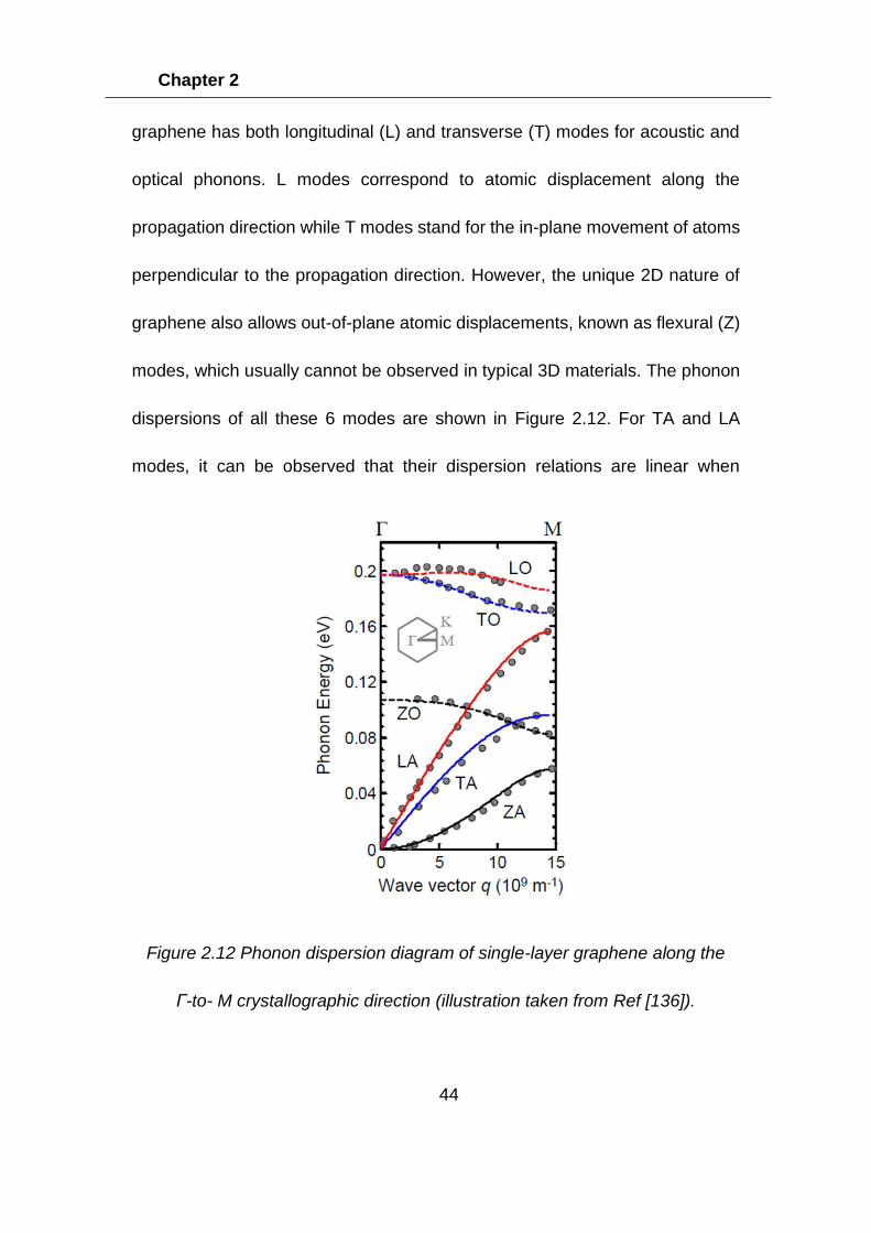
Chapter 2
44
graphene has both longitudinal (L) and transverse (T) modes for acoustic and
optical phonons. L modes correspond to atomic displacement along the
propagation direction while T modes stand for the in-plane movement of atoms
perpendicular to the propagation direction. However, the unique 2D nature of
graphene also allows out-of-plane atomic displacements, known as flexural (Z)
modes, which usually cannot be observed in typical 3D materials. The phonon
dispersions of all these 6 modes are shown in Figure 2.12. For TA and LA
modes, it can be observed that their dispersion relations are linear when
Figure 2.12 Phonon dispersion diagram of single-layer graphene along the
Γ-to- M crystallographic direction (illustration taken from Ref [136]).
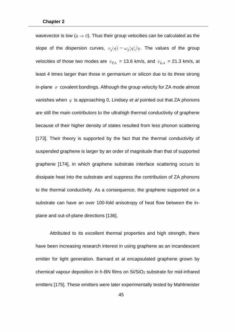
Chapter 2
45
wavevector is low ( ). Thus their group velocities can be calculated as the
slope of the dispersion curves, . The values of the group
velocities of those two modes are = 13.6 km/s, and = 21.3 km/s, at
least 4 times larger than those in germanium or silicon due to its three strong
in-plane covalent bondings. Although the group velocity for ZA mode almost
vanishes when is approaching 0, Lindsey et al pointed out that ZA phonons
are still the main contributors to the ultrahigh thermal conductivity of graphene
because of their higher density of states resulted from less phonon scattering
[173]. Their theory is supported by the fact that the thermal conductivity of
suspended graphene is larger by an order of magnitude than that of supported
graphene [174], in which graphene substrate interface scattering occurs to
dissipate heat into the substrate and suppress the contribution of ZA phonons
to the thermal conductivity. As a consequence, the graphene supported on a
substrate can have an over 100-fold anisotropy of heat flow between the in-
plane and out-of-plane directions [136].
Attributed to its excellent thermal properties and high strength, there
have been increasing research interest in using graphene as an incandescent
emitter for light generation. Barnard et al encapsulated graphene grown by
chemical vapour deposition in h-BN films on Si/SiO2 substrate for mid-infrared
emitters [175]. These emitters were later experimentally tested by Mahlmeister
Chapter 2
46
et al with a measurable modulation speed observed at 100kHz [19]. Kim et al
fabricated the light source based on freely suspended, mechanically exfoliated
graphene flakes [176]. One of the most fascinating phenomena of graphene
emitters is the formation of the hotspot, where maximum emission occurs, and
which can be manipulated by the gate voltage when a large source-drain
current is applied [177]. As introduced in the electronic properties of graphene,
the gate doping can introduce holes or electrons into the graphene channel.
The gate voltage is equal to Dirac voltage of the graphene when the carrier
density in graphene reaches a minimum (charge neutral point (CNP)) where
the graphene has its maximum resistivity. Freitag et al found the Dirac voltage
along the graphene channel becomes position dependant when a source-drain
current is applied. By setting a constant gate voltage, one can manipulate the
position where Dirac voltage is equal to gate voltage by change the source drain
current. As consequence, a hot-spot (heat maximum) will be observed in Figure
2.13 (a) at the position where the CNP is located (hotspot). However, the
hotspots are usually spatially broad and thus make their positions challenging
to be fine-tuned. Bae et al enhance the capacitive coupling between the back
gate and the charge carriers in the channel by reducing the thickness of
underneath oxide layer to 90 nm, the thermal distribution, as shown in Figure
2.13(d) become more localized and sharper [178].
Chapter 2
47
Figure 2.13 (a) Spatial images of the integrated infrared emission from
graphene channels with different gate voltage, (b) Corresponding I-V
characteristic, (c) Infrared intensity profile along the length of the graphene
sample, (d) More localized hotspot with bias graphene on a substrate with
thinner oxidized layer ((a-c) taken from Ref. [177], (d) taken from Ref.
[178]).
Chapter 3
48
3 Numerical Simulations
Introduction
Numerical modelling plays a critical role in the study of optoelectronic
devices for identifying new structures in the development of novel or improved
applications. The most obvious advantage of numerical simulations is that it
assists the prediction and optimisation of the design behaviour without
unnecessary fabrication iterations, saving researcher lots of time and effort. It
also provides such key information as field distribution, current density and far-
field projection that cannot be easily measured in experiments. In this chapter,
we will mainly focus on two most popular technique for solving electromagnetic
problems, the finite element method (FEM) and the finite-difference time-
domain (FDTD) method, as the device studied in this thesis were all simulated
by these two mathematical modelling methods. We will first briefly introduce
both algorithms and then discuss how to set up the material property, mesh
size, boundary conditions in two commercial software package, COMSOL
Multiphysics based on FEM and Lumerical FDTD Solutions based on FDTD
method. These settings are crucial for us to build a valid simulation model and
obtain a reliable, accurate simulation result.
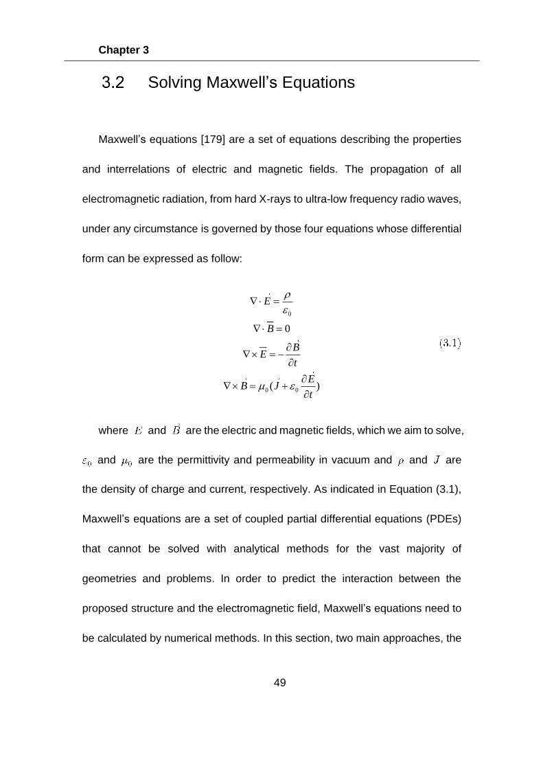
Chapter 3
49
Solving Maxwell’s Equations
Maxwell’s equations [179] are a set of equations describing the properties
and interrelations of electric and magnetic fields. The propagation of all
electromagnetic radiation, from hard X-rays to ultra-low frequency radio waves,
under any circumstance is governed by those four equations whose differential
form can be expressed as follow:
0
0 0
0
( )
E
B
BE
t
EB J
t
=
=
= −
= +
where and are the electric and magnetic fields, which we aim to solve,
and are the permittivity and permeability in vacuum and and are
the density of charge and current, respectively. As indicated in Equation (3.1),
Maxwell’s equations are a set of coupled partial differential equations (PDEs)
that cannot be solved with analytical methods for the vast majority of
geometries and problems. In order to predict the interaction between the
proposed structure and the electromagnetic field, Maxwell’s equations need to
be calculated by numerical methods. In this section, two main approaches, the
Chapter 3
50
FEM [180] as well as the FDTD method [181], for solving the differential
equations are discussed. Although apart from these two numerical methods
focusing on solving Maxwell’s equations in differential form, there are other
means like the method of moments (MoM) [182], the finite integration technique
(FIT) [183], the finite-difference frequency-domain (FDFD) method [184] can
serve the same purpose under certain circumstances. However, those
techniques suffer from disadvantages [185] which makes them not as common
as the FEM and the FDTD method.
Finite Element Method
The development of the FEM can be traced back to early 1940s when
Richard Courant first proposed this method in solving torsion problems for
multiply-connected domains [186]. Although he recognized such method can
be applied to solve a range of problems, it took several decades before the
approach became widely used in solving space-dependent problems which can
usually be expressed in terms of PDEs. In the FEM, the target PDE over the
desired solution domain is discretized in small regions, known as finite elements.
For instance, as illustrated in Figure 3.1, in 2D applications, the domain is
normally discretized into triangles while the most common shape of finite
element for 3D models is tetrahedron. Such shapes of FEM elements provide
Chapter 3
51
advantages on modelling structures with irregular geometries and capturing
local effects. The numbered vertices of each created finite element are specific
points (nodes) at which the value of the dependent variables are explicitly
calculated. The calculated values at these nodes are then used to approximate
the values of the dependent variables at non-node points inside the finite
element. The nodes of this element are exterior nodes because they lie on the
element boundary. Multiple elements are then used, connected at the exterior
nodes, to approximate the entire domain geometry. After that, interpolation
functions are selected for elements. Usually, interpolation functions are first,
second or higher-order polynomials. Then, a system of equations is formulated
Figure 3.1 Geometry for 2D and 3D meshes (elements) in COMSOL.
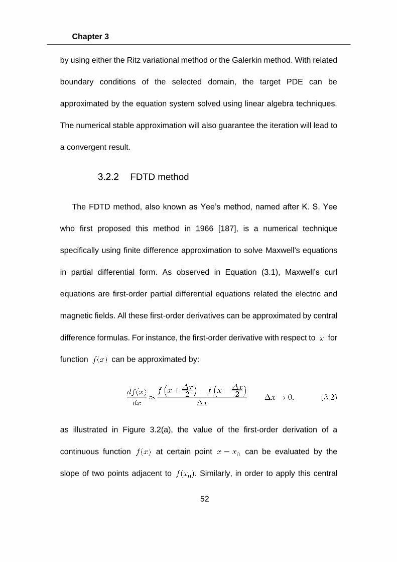
Chapter 3
52
by using either the Ritz variational method or the Galerkin method. With related
boundary conditions of the selected domain, the target PDE can be
approximated by the equation system solved using linear algebra techniques.
The numerical stable approximation will also guarantee the iteration will lead to
a convergent result.
FDTD method
The FDTD method, also known as Yee’s method, named after K. S. Yee
who first proposed this method in 1966 [187], is a numerical technique
specifically using finite difference approximation to solve Maxwell's equations
in partial differential form. As observed in Equation (3.1), Maxwell’s curl
equations are first-order partial differential equations related the electric and
magnetic fields. All these first-order derivatives can be approximated by central
difference formulas. For instance, the first-order derivative with respect to for
function can be approximated by:
as illustrated in Figure 3.2(a), the value of the first-order derivation of a
continuous function at certain point can be evaluated by the
slope of two points adjacent to . Similarly, in order to apply this central
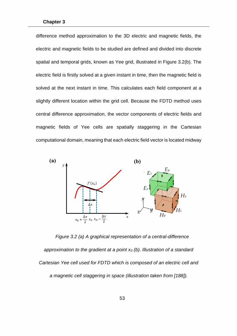
Chapter 3
53
difference method approximation to the 3D electric and magnetic fields, the
electric and magnetic fields to be studied are defined and divided into discrete
spatial and temporal grids, known as Yee grid, illustrated in Figure 3.2(b). The
electric field is firstly solved at a given instant in time, then the magnetic field is
solved at the next instant in time. This calculates each field component at a
slightly different location within the grid cell. Because the FDTD method uses
central difference approximation, the vector components of electric fields and
magnetic fields of Yee cells are spatially staggering in the Cartesian
computational domain, meaning that each electric field vector is located midway
Figure 3.2 (a) A graphical representation of a central-difference
approximation to the gradient at a point x0 (b). Illustration of a standard
Cartesian Yee cell used for FDTD which is composed of an electric cell and
a magnetic cell staggering in space (illustration taken from [188]).
Chapter 3
54
between a pair of magnetic field vectors, and vice versa. Furthermore, as H-
fields are sampled at a half sampling interval difference than that of E-fields
sampling, E-fields and H-fields are updated in a leapfrog scheme for marching
forward in time. The process is repeated over and over until the desired
transient or steady-state electromagnetic field behaviour is fully evolved.
This algorithm is capable of finding the corresponding electric and magnetic
fields and at any point in space for any time with any given
excitation source. Because it solves the problem in the time domain, a wide
range frequency as well as a fine frequency resolution can be obtained through
Fourier transform. This is extremely useful in applications where resonant
frequencies are not exactly known, or anytime that a broadband result is
desired.
Simulation software and settings
Simulation Software
Although both the FEM and the FDTD method offer proven approaches to
numerically calculate the interaction between any artificial design and
electromagnetic field, it still needs a vast material, financial support, manpower
Chapter 3
55
and time to build a generalized 3D electromagnetic solver which contains the
full 6-vector Maxwell's equations. Thanks to the progress in computer
technology, various commercial software with automatic adaptive and graphical
user interface (GUI) features nowadays can provide a fast, stable, accurate and
multifunction EM simulator. The software packages which we chose in the
simulations are COMSOL Multiphysics and Lumerical FDTD Solutions.
COMSOL Multiphysics is a general-purpose simulation software based on
FEM analyses for modelling designs, devices, and processes in all fields of
engineering, manufacturing, and scientific research. The module mainly used
in the simulations described in this thesis is the RF module. It provides a
simulation environment to solve PDEs not only for electromagnetics but also
for heat transfer, structure deformation, fluid flow, and so on. The commercial
software chosen for the FDTD method is Lumerical FDTD Solutions, which is a
leading 2D/3D Maxwell’s equation solver for the design, analysis, and
optimization of nanophotonic devices, processes and materials. It implements
the FDTD method to analyze the interaction of a broad spectrum of radiation
with complicated designs and deliver reliable results.
With the help of the powerful commercial software, we still need to make the
right configurations on our model to obtain a trustworthy simulation result. The
Chapter 3
56
following paragraphs will mainly focus on the settings on material properties,
boundary conditions and mesh sizes.
Material Properties
The most important settings of material properties are similar in both
COMSOL Multiphysics and Lumerical FDTD Solutions. As the type of materials
to be defined can usually be chosen from a list. Here we will list some of the
most common materials.
i) Dielectric
For most non-conductive materials, the materials can be defined as ‘(n,k)
material’ in Lumerical FDTD Solutions and ‘refractive index’ as the
displacement field model applied on the material in COMSOL Multiphysics. In
this case, the refractive index of the material will simply be modelled as
, where and are the real and imaginary part of the refractive index.
The value of is usually positive which corresponds to the energy loss in the
wave propagation. If the refractive index of the dielectric material is dispersive
over the frequency of interest, its frequency dependant and can be
extracted from the metrology of the material, like ellipsometry or
spectrophotometer [189]. The result refractive index datasets can be loaded to
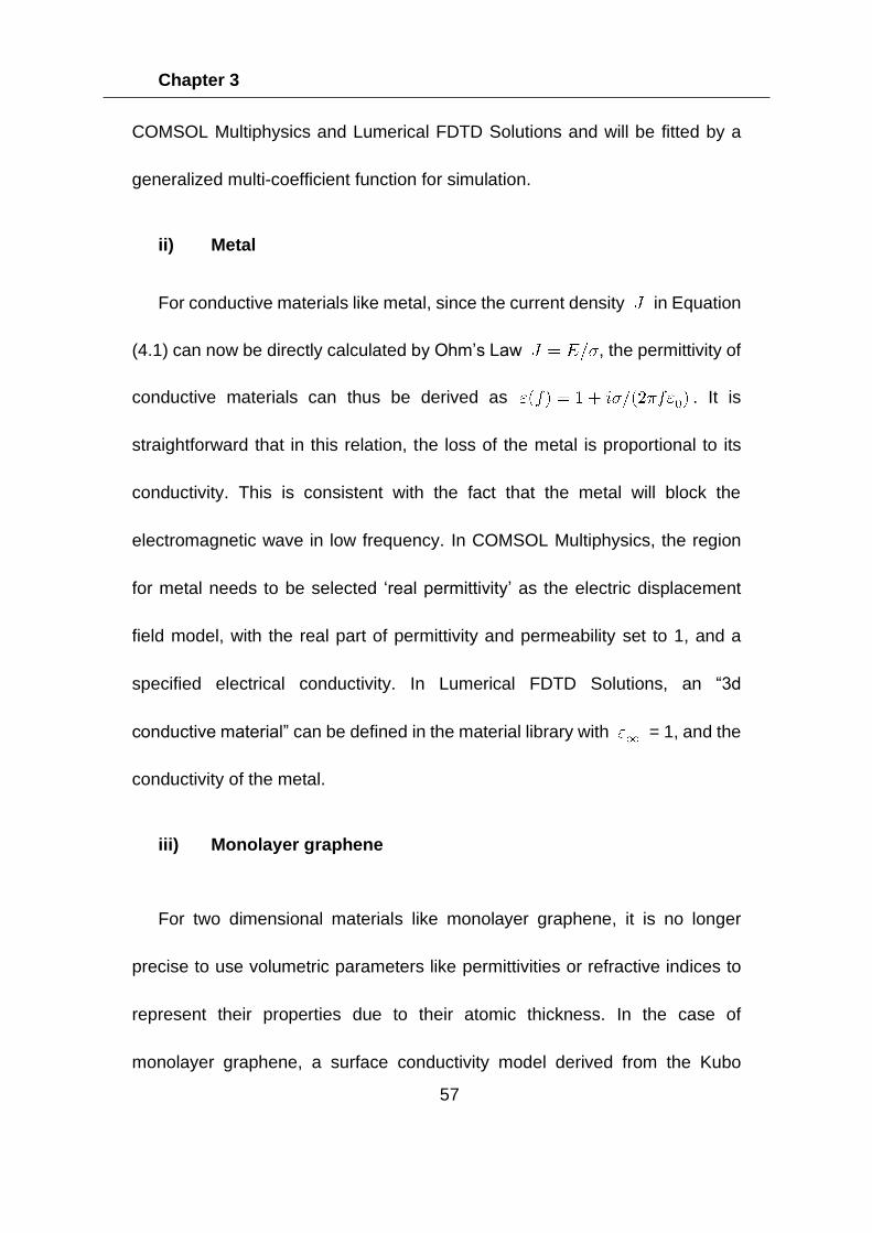
Chapter 3
57
COMSOL Multiphysics and Lumerical FDTD Solutions and will be fitted by a
generalized multi-coefficient function for simulation.
ii) Metal
For conductive materials like metal, since the current density in Equation
(4.1) can now be directly calculated by Ohm’s Law , the permittivity of
conductive materials can thus be derived as . It is
straightforward that in this relation, the loss of the metal is proportional to its
conductivity. This is consistent with the fact that the metal will block the
electromagnetic wave in low frequency. In COMSOL Multiphysics, the region
for metal needs to be selected ‘real permittivity’ as the electric displacement
field model, with the real part of permittivity and permeability set to 1, and a
specified electrical conductivity. In Lumerical FDTD Solutions, an “3d
conductive material” can be defined in the material library with = 1, and the
conductivity of the metal.
iii) Monolayer graphene
For two dimensional materials like monolayer graphene, it is no longer
precise to use volumetric parameters like permittivities or refractive indices to
represent their properties due to their atomic thickness. In the case of
monolayer graphene, a surface conductivity model derived from the Kubo
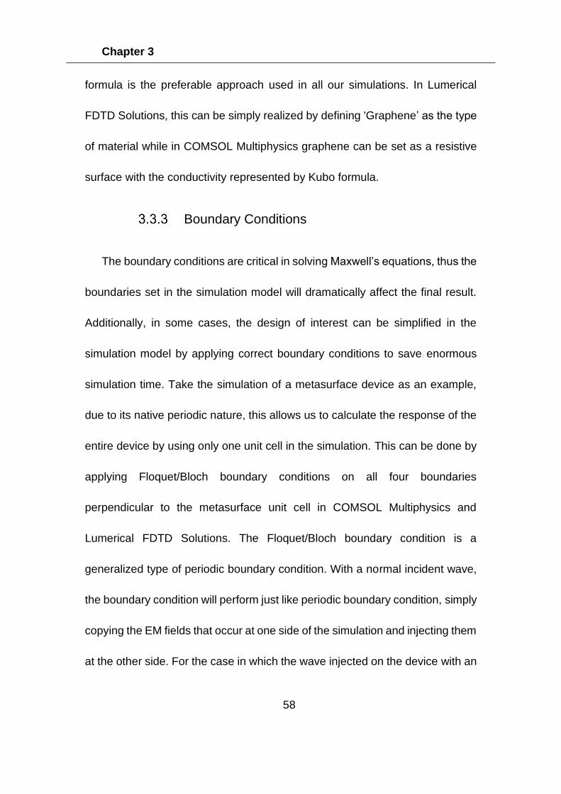
Chapter 3
58
formula is the preferable approach used in all our simulations. In Lumerical
FDTD Solutions, this can be simply realized by defining 'Graphene’ as the type
of material while in COMSOL Multiphysics graphene can be set as a resistive
surface with the conductivity represented by Kubo formula.
Boundary Conditions
The boundary conditions are critical in solving Maxwell’s equations, thus the
boundaries set in the simulation model will dramatically affect the final result.
Additionally, in some cases, the design of interest can be simplified in the
simulation model by applying correct boundary conditions to save enormous
simulation time. Take the simulation of a metasurface device as an example,
due to its native periodic nature, this allows us to calculate the response of the
entire device by using only one unit cell in the simulation. This can be done by
applying Floquet/Bloch boundary conditions on all four boundaries
perpendicular to the metasurface unit cell in COMSOL Multiphysics and
Lumerical FDTD Solutions. The Floquet/Bloch boundary condition is a
generalized type of periodic boundary condition. With a normal incident wave,
the boundary condition will perform just like periodic boundary condition, simply
copying the EM fields that occur at one side of the simulation and injecting them
at the other side. For the case in which the wave injected on the device with an
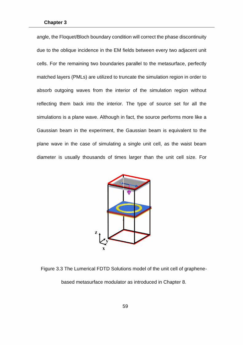
Chapter 3
59
angle, the Floquet/Bloch boundary condition will correct the phase discontinuity
due to the oblique incidence in the EM fields between every two adjacent unit
cells. For the remaining two boundaries parallel to the metasurface, perfectly
matched layers (PMLs) are utilized to truncate the simulation region in order to
absorb outgoing waves from the interior of the simulation region without
reflecting them back into the interior. The type of source set for all the
simulations is a plane wave. Although in fact, the source performs more like a
Gaussian beam in the experiment, the Gaussian beam is equivalent to the
plane wave in the case of simulating a single unit cell, as the waist beam
diameter is usually thousands of times larger than the unit cell size. For
Figure 3.3 The Lumerical FDTD Solutions model of the unit cell of graphene-
based metasurface modulator as introduced in Chapter 8.
Chapter 3
60
example, in the case shown in Figure 3.3, the wave propagates along the z-
axis. Thus all the x-z boundaries and y-z boundaries in the black rectangle are
set for Floquet/Bloch boundary conditions to make the design periodic in x- and
y-axis directions. Meanwhile, all the x-y boundaries in the red rectangle are set
for PML boundaries to eliminate the reflection from the top and bottom of the
simulation region.
Mesh sizes
Another critical parameter in both simulation software packages is the mesh
size. As mentioned in Section 3.2, both methods are based on discretizing the
model into smaller units (elements for the FEM and Yee cells for the FDTD
method). Although a finer mesh may provide a more accurate result, it will also
significantly increase the simulation time and memory usage in the meantime.
The memory usage for a 3D model whose volume is with a mesh step size
at certain wavelength is approximately and simulation time is
around [190]. Thus finding an appropriate mesh size to balance the
result accuracy and simulation time is always a challenging work in every
simulation model. Generally speaking, the mesh size should be at least smaller
than half of the wavelength in the medium and the maximum size of meshes is
approximately one-fifth of the wavelength in the medium. For both commercial
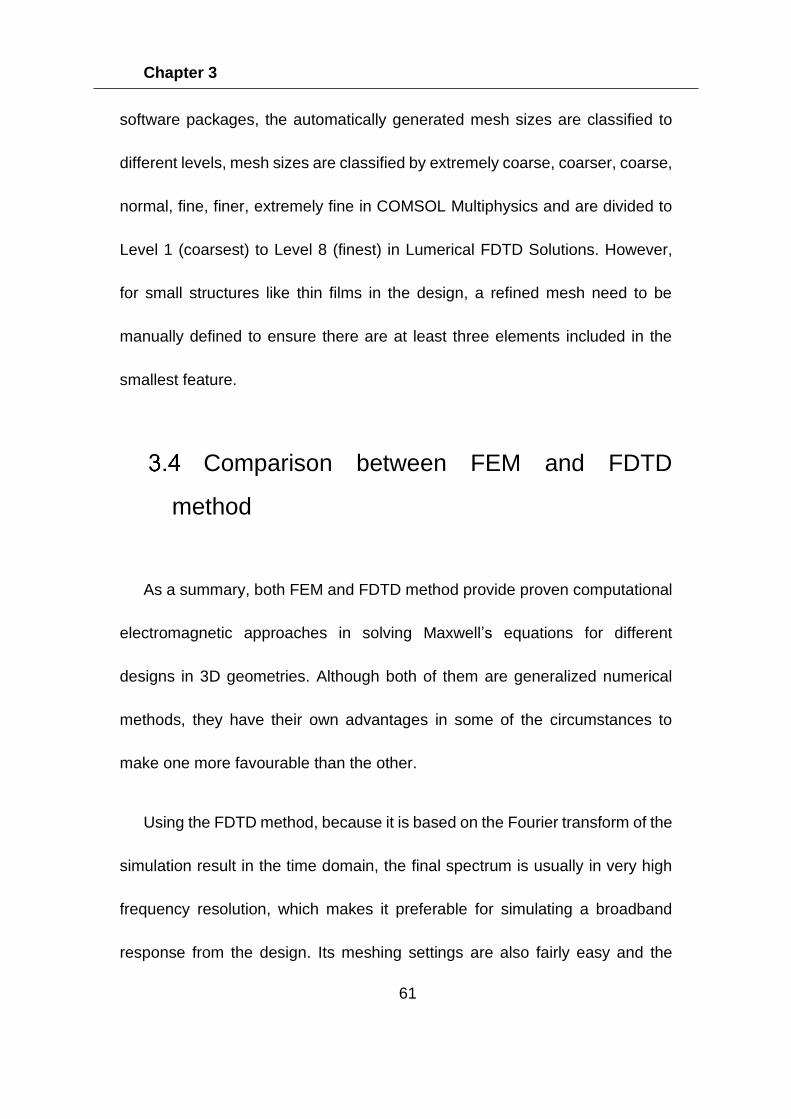
Chapter 3
61
software packages, the automatically generated mesh sizes are classified to
different levels, mesh sizes are classified by extremely coarse, coarser, coarse,
normal, fine, finer, extremely fine in COMSOL Multiphysics and are divided to
Level 1 (coarsest) to Level 8 (finest) in Lumerical FDTD Solutions. However,
for small structures like thin films in the design, a refined mesh need to be
manually defined to ensure there are at least three elements included in the
smallest feature.
Comparison between FEM and FDTD
method
As a summary, both FEM and FDTD method provide proven computational
electromagnetic approaches in solving Maxwell’s equations for different
designs in 3D geometries. Although both of them are generalized numerical
methods, they have their own advantages in some of the circumstances to
make one more favourable than the other.
Using the FDTD method, because it is based on the Fourier transform of the
simulation result in the time domain, the final spectrum is usually in very high
frequency resolution, which makes it preferable for simulating a broadband
response from the design. Its meshing settings are also fairly easy and the
Chapter 3
62
simulation won’t use so much memory compared to the FEM. However, simple
meshes are also less suitable when discretizing curved edges or sharp corners.
The staircase approximation error in meshing may lead to an error in the
simulation results. The oblique incident will cause major difficulty in
implementation of the FDTD method because the phase difference between
corresponding points in different unit cells lead into time advance or delay that
cannot be solved directly using the time-domain method. This delay requires
knowledge of the future values of the fields at any step in the transverse plane
which makes the FDTD method, the method depends mainly on the
simultaneous time and space, difficult to implement the oblique source.
In contrast, the FEM can also realize simulation covering a broadband
frequency range. It normally divides the frequency range into several steps,
runs the simulation at each discrete frequency and combines several discrete
results into a spectrum result. This makes the FEM far less efficient comparing
to the FDTD method. Furthermore, the meshing in COMSOL Multiphysics
sometimes can be problematic and occupy a large amount of memory in PC,
especially for some structures including anisotropic geometries like ultrathin
films. However, the complicated mesh also has some advantages, it represents
the original structure much better than FDTD meshes as shown in Figure 3.4,
and leads to a more precise result. Apart from this advantage, for COMSOL
Chapter 3
63
Multiphysics, we can use Multiphysics function to take other effects like heat
transfer, chemical reaction, etc into the consideration of the simulation.
The simulation results shown in Chapter 6 & 8 all used Lumerical FDTD
Solutions as the simulation engine while the results in Chapter 7 used COMSOL
Multiphysics because of the oblique incidence of the wave on the prism.
Figure 3.4 The automatically generated mesh for a sphere with 5 μm radius
in (a) Lumerical FDTD Solutions (mesh setting: level 4) and (b) COMSOL
Multiphysics (mesh setting: normal).
Chapter 4
64
4 Device Fabrication
Introduction
Due to the fact that the scale of mid-infrared metasurface devices is usually
in the order of sub-micrometers, high precision in fabrication is required to
realize devices. Thanks to the significant advances in lithography technology in
the past decade, which has dramatically shrunk the size of devices that can be
achieved, the discoveries of nanoscience can be implemented in real-world
nanoscale devices. In this chapter, we will introduce the nanofabrication
techniques involved in the fabrication of our devices. The lithography,
deposition and lift-off processes for metasurface fabrication and transfer,
etching processes for 2D materials like graphene, and h-BN will be discussed
in Section 4.2 and 4.3, respectively. Finally, in Section 4.4, a list of all the
fabricated devices used in the experiments presented in this work is provided.
All the devices presented in this thesis are all fabricated in an ISO Class 5
cleanroom, whose temperature and humidity are strictly controlled to ensure
the precision of fabrication.
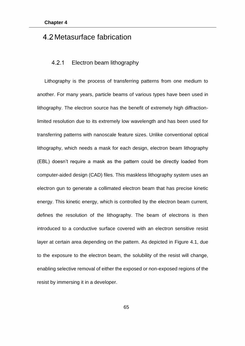
Chapter 4
65
Metasurface fabrication
Electron beam lithography
Lithography is the process of transferring patterns from one medium to
another. For many years, particle beams of various types have been used in
lithography. The electron source has the benefit of extremely high diffraction-
limited resolution due to its extremely low wavelength and has been used for
transferring patterns with nanoscale feature sizes. Unlike conventional optical
lithography, which needs a mask for each design, electron beam lithography
(EBL) doesn’t require a mask as the pattern could be directly loaded from
computer-aided design (CAD) files. This maskless lithography system uses an
electron gun to generate a collimated electron beam that has precise kinetic
energy. This kinetic energy, which is controlled by the electron beam current,
defines the resolution of the lithography. The beam of electrons is then
introduced to a conductive surface covered with an electron sensitive resist
layer at certain area depending on the pattern. As depicted in Figure 4.1, due
to the exposure to the electron beam, the solubility of the resist will change,
enabling selective removal of either the exposed or non-exposed regions of the
resist by immersing it in a developer.
Chapter 4
66
In the lithography process, there are three main important parameters for
that need to be optimized for a reliable fabrication recipe: beam current,
exposure dose and development time. The beam current defines the resolution
of the exposure, and normally needs to be set corresponding to the smallest
geometric feature in the design. Although smaller beam current can give us
higher spatial resolution in fabrication, it will take much longer time in doing the
lithography and thus result in low production efficiency. Exposure dose,
together with the beam current determine how many electrons are emitted from
the gun per unit area, which is directly relevant to the pattern quality.
Development time is another crucial parameter that needs to be controlled
precisely. The resist will not dissolve completely if the sample is
underdeveloped, and the pattern will be distorted if overdeveloped. There are
Figure 4.1 Schematic diagrams of the lithography processes on positive
resist (top row) or negative resist (bottom row).
Chapter 4
67
also other parameters that could affect the quality of a lithography process,
such as resist types, the thickness of the resist, developer concentration, and
so on.
In our device fabrication process, the EBL system used is a Nanobeam nB4
system which is able to attain a minimum beam current as low as 1 nA, and the
photoresist chosen is 6% single layer polymethyl methacrylate with 950,000
molecule weight in anisole (950K PMMA, A6), which is spun on the prebaked
substrate in a spinner at 4000rpm to form a uniform 400 nm-thick positive resist
layer. After exposing in the EBL, the sample is rinsed for 40 seconds in a
solution of isopropyl alcohol (IPA), methyl iso-butyl ketone (MIBK) and methyl
ethyl ketone (MEK) in a ratio of IPA:MIBK:MEK = 3:1:0.2. before placing in IPA
to wash the developer away and blowing dry by nitrogen. Finally the sample will
be inspected using optical microscopy, and is then ready for post-processing
like etching or metallization. The aforementioned parameters of dosage, beam
current, development time, and concentration of the developer in the recipe
were optimized through dose tests and proved to downscale the pattern
resolution to ~50 nm.
Chapter 4
68
Metallization
Metallization is required to form the metallic structure based on the
patterned PMMA resist after the lithography process. This normally includes
two main steps, coating and lift-off. Sputtering and thermal evaporation are the
two most common ways to deposit metal material on a sample. A sputter
generates energetic ions to collide with a metal target to thus eject target
material, while the thermal evaporator relies on heating the metallic
material over the vaporization temperature. Although, in theory, sputtering
can form a metallic layer with higher uniformity and purity than thermal
evaporation, thermal evaporation was chosen for all the graphene devices as
the high energy of the sputter atoms will inevitably cause damage to the
graphene on the substrate for all the graphene-integrated devices. The thermal
evaporator used in the fabrication process is an HHV Auto306 Thermal
Evaporator, which is able to evaporate up to 4 different kinds of metal at one
time. In the device fabrication, gold is chosen as the material for metamaterial
structure as well as the contacts due to its high conductivity. However, due to
the poor adhesion of the gold layer on the substrate, a thin layer of chromium
is needed to be deposited as the adhesion layer before the gold layer is coated.
The thickness of the Cr layer is usually about 5-10 nm, not thick enough to alter
the property of the fabricated device, but helps to prevent gold from flaking off
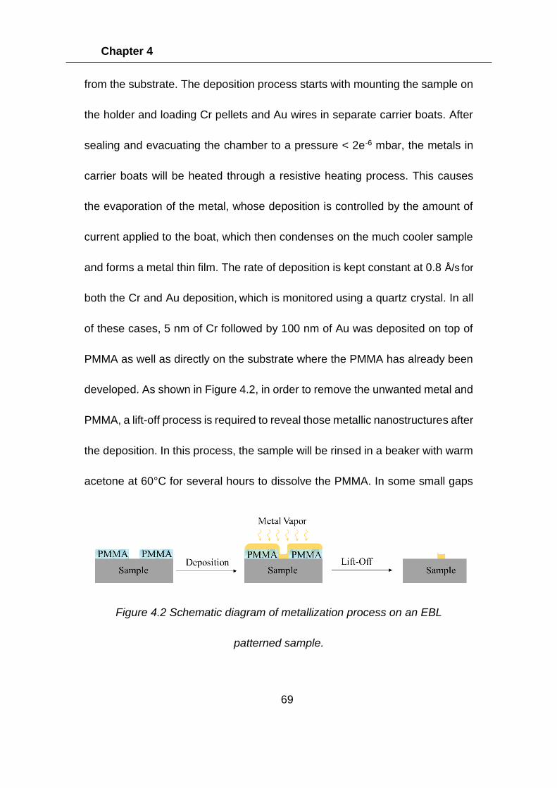
Chapter 4
69
from the substrate. The deposition process starts with mounting the sample on
the holder and loading Cr pellets and Au wires in separate carrier boats. After
sealing and evacuating the chamber to a pressure < 2e-6 mbar, the metals in
carrier boats will be heated through a resistive heating process. This causes
the evaporation of the metal, whose deposition is controlled by the amount of
current applied to the boat, which then condenses on the much cooler sample
and forms a metal thin film. The rate of deposition is kept constant at 0.8 Å/s for
both the Cr and Au deposition, which is monitored using a quartz crystal. In all
of these cases, 5 nm of Cr followed by 100 nm of Au was deposited on top of
PMMA as well as directly on the substrate where the PMMA has already been
developed. As shown in Figure 4.2, in order to remove the unwanted metal and
PMMA, a lift-off process is required to reveal those metallic nanostructures after
the deposition. In this process, the sample will be rinsed in a beaker with warm
acetone at 60°C for several hours to dissolve the PMMA. In some small gaps
Figure 4.2 Schematic diagram of metallization process on an EBL
patterned sample.
Chapter 4
70
where the acetone is unable to dissolve PMMA entirely covered by metallic
sidewalls, an ultrasonicator is needed to aid in the lift-off process.
2D-material fabrication
2D material transfer
Apart from metasurface, another group of nanoscale constituents in most of
the devices discussed in this thesis is 2D materials which include graphene and
hexagonal boron nitride (h-BN). Due to the recent progress in synthesizing 2D
materials through chemical vapour deposition (CVD), large-area 2D materials,
which can never be realized by conventional mechanical exfoliation method,
are now commercially available [191]. Mono- and multi-layer CVD 2D materials
like graphene and h-BN are all commercially available through multiple outlets
and are widely used for research purpose. However, the CVD method usually
requires a metal substrate such as Cu, Ni, Al [192,193], to form 2D materials,
so 2D materials need to be transferred on an appropriate substrate before
device fabrication. For all the fabrication described in this thesis, all CVD 2D
materials used are grown on copper foil (from Graphene Supermarket) and
Si/SiO2 substrate is the target substrate on which the devices are fabricated.
To achieve transferring 2D materials grown on Cu foil to Si/SiO2 substrate, the
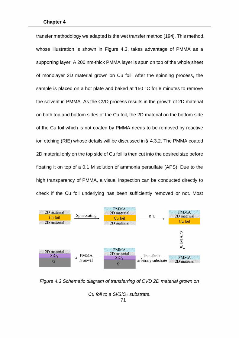
Chapter 4
71
transfer methodology we adapted is the wet transfer method [194]. This method,
whose illustration is shown in Figure 4.3, takes advantage of PMMA as a
supporting layer. A 200 nm-thick PMMA layer is spun on top of the whole sheet
of monolayer 2D material grown on Cu foil. After the spinning process, the
sample is placed on a hot plate and baked at 150 °C for 8 minutes to remove
the solvent in PMMA. As the CVD process results in the growth of 2D material
on both top and bottom sides of the Cu foil, the 2D material on the bottom side
of the Cu foil which is not coated by PMMA needs to be removed by reactive
ion etching (RIE) whose details will be discussed in § 4.3.2. The PMMA coated
2D material only on the top side of Cu foil is then cut into the desired size before
floating it on top of a 0.1 M solution of ammonia persulfate (APS). Due to the
high transparency of PMMA, a visual inspection can be conducted directly to
check if the Cu foil underlying has been sufficiently removed or not. Most
Figure 4.3 Schematic diagram of transferring of CVD 2D material grown on
Cu foil to a Si/SiO2 substrate.
Chapter 4
72
importantly, because of the flexibility and dissolubility to etchant of PMMA, the
2D material with PMMA on top will remain floating on top of the solution when
the Cu foil is totally etched. This is then scooped out with a glass spoon and
then rinsed in DI water six times, based on a standard recipe, in order to remove
any remaining etchant residue. This PMMA covered 2D material is then
transferred to the Si/SiO2 substrate and finally removed with warm acetone after
the water between the Si/SiO2 substrate and 2D material is completely dried
out in the air.
Reactive ion etching
RIE, in conjunction with EBL, is used in order to pattern the 2D materials
into desired shapes. EBL process as described in § 4.2.1 is firstly conducted
on the Si/SiO2 substrate with CVD 2D material(s) on top and will leave a layer
of patterned PMMA which will act as a hard mask later in RIE. The RIE process
is a high-resolution etching process based on reactive gas discharges. Specific
process gases are introduced into the vacuum chamber and then ionized by
radiofrequency (RF) power to form the plasma. Meanwhile, a negative DC bias
is applied on the substrate plate to accelerate the positively charged ions
colliding with the negatively biased sample on the plate and results into a high
anisotropic, selectivity etch profile.
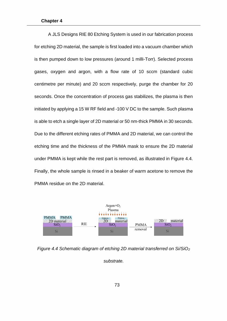
Chapter 4
73
A JLS Designs RIE 80 Etching System is used in our fabrication process
for etching 2D material, the sample is first loaded into a vacuum chamber which
is then pumped down to low pressures (around 1 milli-Torr). Selected process
gases, oxygen and argon, with a flow rate of 10 sccm (standard cubic
centimetre per minute) and 20 sccm respectively, purge the chamber for 20
seconds. Once the concentration of process gas stabilizes, the plasma is then
initiated by applying a 15 W RF field and -100 V DC to the sample. Such plasma
is able to etch a single layer of 2D material or 50 nm-thick PMMA in 30 seconds.
Due to the different etching rates of PMMA and 2D material, we can control the
etching time and the thickness of the PMMA mask to ensure the 2D material
under PMMA is kept while the rest part is removed, as illustrated in Figure 4.4.
Finally, the whole sample is rinsed in a beaker of warm acetone to remove the
PMMA residue on the 2D material.
Figure 4.4 Schematic diagram of etching 2D material transferred on Si/SiO2
substrate.
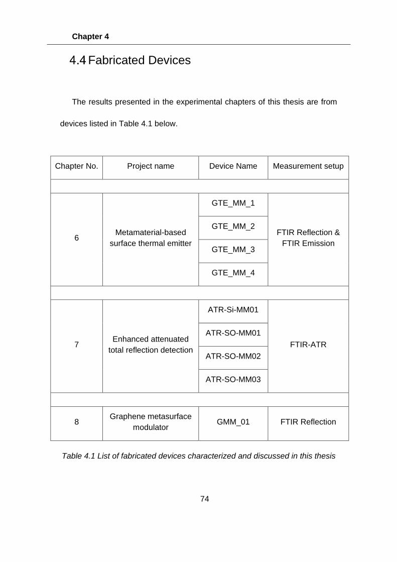
Chapter 4
74
Fabricated Devices
The results presented in the experimental chapters of this thesis are from
devices listed in Table 4.1 below.
Chapter No. Project name Device Name Measurement setup
6 Metamaterial-based
surface thermal emitter
GTE_MM_1
FTIR Reflection &
FTIR Emission
GTE_MM_2
GTE_MM_3
GTE_MM_4
7 Enhanced attenuated
total reflection detection
ATR-Si-MM01
FTIR-ATR
ATR-SO-MM01
ATR-SO-MM02
ATR-SO-MM03
8 Graphene metasurface
modulator GMM_01 FTIR Reflection
Table 4.1 List of fabricated devices characterized and discussed in this thesis
Chapter 5
75
5 Characterisation
Introduction
This chapter mainly focuses on introducing the equipment used in testing
the fabricated samples, both for morphology and spectroscopic characterization.
Three common microscopy technologies for assessing nanoscale structures,
optical microscope, scanning electron microscope (SEM) and atomic force
microscope (AFM) are introduced and compared in Section 5.2. Section 5.3
describes a series of spectroscopic measurement setups based on a Bruker
Vertex 80v FTIR spectrometer. More details on the measurement steps for
acquiring the transmission, reflection or emission spectrum can be found in §
5.3.1-5.3.3. The attenuated total reflection (ATR) measurement setup is also
presented in § 5.3.4. This technique is particularly useful when measuring
samples in liquid form.
Chapter 5
76
Metrology
Optical Microscopy
Optical microscopy, as the name suggests, utilizes light and optical systems
to visualize objects of small sizes that are not visible to the human eye. As the
oldest form of microscopy, it does not compete with modern microscopy
techniques such as electron-based SEM and TEM or laser-based AFM.
Nonetheless, optical microscopy requires no sample preparation and does not
suffer from charging issues; it serves as a good candidate in checking sample
morphology on large scales.
A Nikon LV150 upright optical microscope equipped with 5×, 10×, 20×, 50×
and 100× bright field objective lenses as well as camera operated in reflective
light mode was used in this study.
Scanning Electron Microscopy
Due to the fact that most of the smallest features in the metasurface
structures designed and fabricated in this thesis are the size of several hundred
nanometers, which is below the resolution limit of optical microscopes, the
nanoscale structures cannot be directly observed under the optical microscope
even with its maximum magnification. In order to inspect and measure the
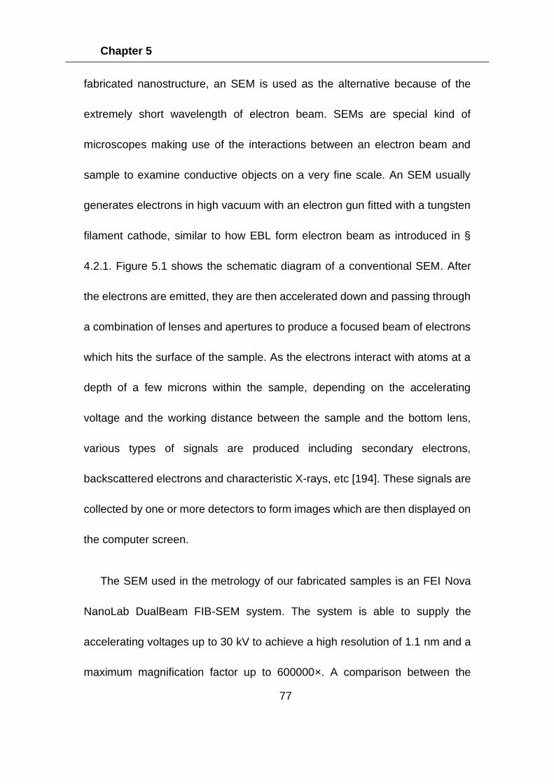
Chapter 5
77
fabricated nanostructure, an SEM is used as the alternative because of the
extremely short wavelength of electron beam. SEMs are special kind of
microscopes making use of the interactions between an electron beam and
sample to examine conductive objects on a very fine scale. An SEM usually
generates electrons in high vacuum with an electron gun fitted with a tungsten
filament cathode, similar to how EBL form electron beam as introduced in §
4.2.1. Figure 5.1 shows the schematic diagram of a conventional SEM. After
the electrons are emitted, they are then accelerated down and passing through
a combination of lenses and apertures to produce a focused beam of electrons
which hits the surface of the sample. As the electrons interact with atoms at a
depth of a few microns within the sample, depending on the accelerating
voltage and the working distance between the sample and the bottom lens,
various types of signals are produced including secondary electrons,
backscattered electrons and characteristic X-rays, etc [194]. These signals are
collected by one or more detectors to form images which are then displayed on
the computer screen.
The SEM used in the metrology of our fabricated samples is an FEI Nova
NanoLab DualBeam FIB-SEM system. The system is able to supply the
accelerating voltages up to 30 kV to achieve a high resolution of 1.1 nm and a
maximum magnification factor up to 600000×. A comparison between the
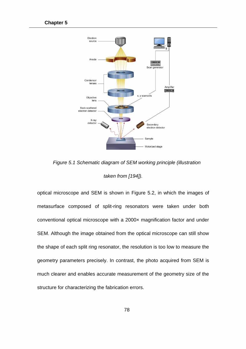
Chapter 5
78
optical microscope and SEM is shown in Figure 5.2, in which the images of
metasurface composed of split-ring resonators were taken under both
conventional optical microscope with a 2000× magnification factor and under
SEM. Although the image obtained from the optical microscope can still show
the shape of each split ring resonator, the resolution is too low to measure the
geometry parameters precisely. In contrast, the photo acquired from SEM is
much clearer and enables accurate measurement of the geometry size of the
structure for characterizing the fabrication errors.
Figure 5.1 Schematic diagram of SEM working principle (illustration
taken from [194]).
Figure 5.1 Schematic diagram of SEM working principle (illustration
taken from [1])

Chapter 5
79
Atomic Force Microscopy
Although the SEM is powerful enough to provide an informative image for
characterizing nanoscale structures on the surface, the image based on the
intensity of the secondary electron emission from the sample at each point
during the raster scanning of the electron beam across the surface does not
contain too many conclusive information in the direction perpendicular to the
surface. In order to measure the height of metasurface on the structure still
under SEM, the sample has to be tilted during the measurement or cross-
sectioned. Both of those methods have obvious drawbacks, the former method
Figure 5.2 Images of a split ring resonator structure proposed in Chapter 8
measured under (a) optical microscope and (b) SEM by using a secondary
electron detector.
Figure 5.2 Images of a split ring resonator structure proposed in
Chapter 8 measured under (a) optical microscope and (b) SEM
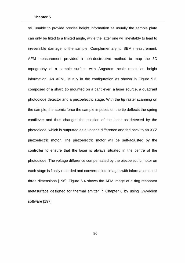
Chapter 5
80
still unable to provide precise height information as usually the sample plate
can only be tilted to a limited angle, while the latter one will inevitably to lead to
irreversible damage to the sample. Complementary to SEM measurement,
AFM measurement provides a non-destructive method to map the 3D
topography of a sample surface with Angstrom scale resolution height
information. An AFM, usually in the configuration as shown in Figure 5.3,
composed of a sharp tip mounted on a cantilever, a laser source, a quadrant
photodiode detector and a piezoelectric stage. With the tip raster scanning on
the sample, the atomic force the sample imposes on the tip deflects the spring
cantilever and thus changes the position of the laser as detected by the
photodiode, which is outputted as a voltage difference and fed back to an XYZ
piezoelectric motor. The piezoelectric motor will be self-adjusted by the
controller to ensure that the laser is always situated in the centre of the
photodiode. The voltage difference compensated by the piezoelectric motor on
each stage is finally recorded and converted into images with information on all
three dimensions [196]. Figure 5.4 shows the AFM image of a ring resonator
metasurface designed for thermal emitter in Chapter 6 by using Gwyddion
software [197].
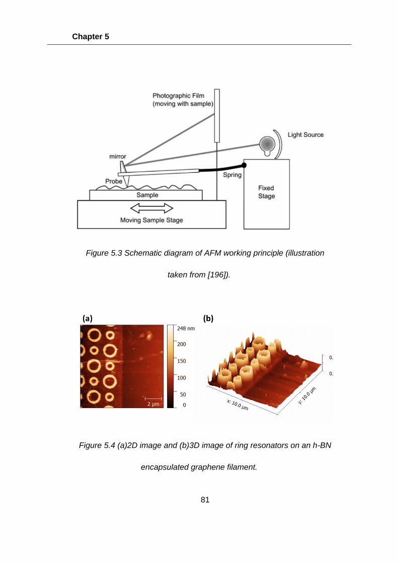
Chapter 5
81
Figure 5.3 Schematic diagram of AFM working principle (illustration
taken from [196]).
Figure 5.4 (a)2D image and (b)3D image of ring resonators on an h-BN
encapsulated graphene filament.
Figure 5.4 (a)2D image and (b)3D image of ring resonators on a h-BN
Chapter 5
82
Electromagnetic response characterization
Transmission Measurement
A state-of-art FTIR spectrometer from Bruker GmBH was used in most of
the experiments conducted in this study to measure the electromagnetic
response of the device in the mid-infrared range. The Bruker FTIR Vertex 80v,
whose schematic is shown in Figure 5.5, is an ideal instrument to measure the
transmission spectrum of the sample. The infrared wave emitted from the
source passes through an aperture wheel which can reduce the beam size
down from 8mm to 0.25mm. The beam with a desired size is then collimated by
a parabolic mirror before entering into the Michelson interferometer composed
of a beamsplitter, a precise linear air bearing scanner [198] and a stationary
mirror. In the interferometer, the beamsplitter transmits half of the wave to the
mirror on the scanner and reflects the remaining half to the stationary mirror.
Since the mirror mounted on the scanner moves, it changes the optical path
length in comparison to the light reflected from the stationary mirror and results
in periodic interference known as interferogram when the beams recombine at
the beamsplitter. The output signal from the interferometer then passes through
the sample compartment and finally the transmission spectra will be obtained
by Fourier transforming the interferogram data recorded at the detector located
Chapter 5
83
at the left side of the sample compartment. The FTIR comes with a wide range
of sources, beamsplitters and detectors which enable the spectra to cover far-
IR, mid-IR, NIR, ranges from 80cm-1 to 7000 cm-1. Because the frequency band
under our interest is mainly mid-IR, globar emitter, KBr beamsplitter, and liquid
nitrogen cooled mercury-cadmium-telluride (MCT) detector are chosen in all the
experiments to ensure high precision measurement between 800 to 4000 cm-1
with a wavenumber resolution less than 1 cm-1 in transmission mode. For the
transmission measurement, a reference spectrum is usually firstly measured
Figure 5.5 Schematic diagram and beam path of a Bruker Vertex 80v FTIR
spectroscopy (illustration taken from [198]).
Figure 5.5 Schematic diagram and beam path of an Bruker Vertex 80v FTIR
spectroscopy (illustration taken from [6]).
Chapter 5
84
without the presence of the sample. After that, the sample is mounted on the
sample holder located at the focal point in the sample compartment for another
transmission spectrum measurement. The transmittance of the sample is
calculated by normalizing the spectrum from the sample to the reference
spectrum. The optical bench can be evacuated rapidly down to a pressure of 3
mbar via a mechanical pump to reduce absorption due to the water vapour and
carbon dioxide in the air.
Reflection measurement
For the measurement in reflection mode, a self-built reflection setup based
on the Bruker FTIR Vertex 80v was built in order to measure the reflection
spectrum of samples, including graphene thermal emitters introduced in
Chapter 6 and graphene modulator presented in Chapter 8. In the reflection
mode which is schematically sketched in Figure 5.6, the computer will control
the internal mirrors in the FTIR to guide the beam from the interferometer to exit
port 4 as illustrated in Figure 5.5 instead of the sample compartment. The size
of the collimated beam is first reduced by using a pair of Au parabolic mirrors.
Then the small collimated beam will pass through another beamsplitter and
later be collected by a 40× reflecting objective lens mounted on a motorized XY
stage, which focused the collimated beam onto the sample. The reflected wave
Chapter 5
85
from the sample will be collimated again by the reflecting objective lens and
then pass through the beamsplitter one more time. The refracted portion will be
focused onto the MCT detector with a third Au parabolic mirror. Unlike in
transmission where one can easily align the area to be measured to the infrared
beam spot which is indicated by the built-in HeNe laser, it is hard to estimate
where the infrared beam is incident on the sample in the reflection mode. In
order to make sure the beam locates on the desired area, a raster scan is
usually run on the sample before the spectrum measurement. However, due to
the existence of the second beamsplitter in the setup as well as the inevitable
misalignment of the system, the reflection signal coming back to the MCT
Figure 5.6 The external setup of FTIR spectroscopy for reflection
measurement.
Figure 5.6
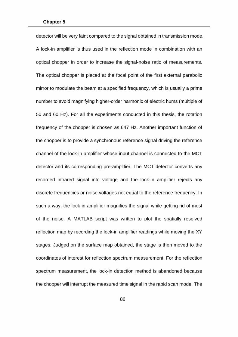
Chapter 5
86
detector will be very faint compared to the signal obtained in transmission mode.
A lock-in amplifier is thus used in the reflection mode in combination with an
optical chopper in order to increase the signal-noise ratio of measurements.
The optical chopper is placed at the focal point of the first external parabolic
mirror to modulate the beam at a specified frequency, which is usually a prime
number to avoid magnifying higher-order harmonic of electric hums (multiple of
50 and 60 Hz). For all the experiments conducted in this thesis, the rotation
frequency of the chopper is chosen as 647 Hz. Another important function of
the chopper is to provide a synchronous reference signal driving the reference
channel of the lock-in amplifier whose input channel is connected to the MCT
detector and its corresponding pre-amplifier. The MCT detector converts any
recorded infrared signal into voltage and the lock-in amplifier rejects any
discrete frequencies or noise voltages not equal to the reference frequency. In
such a way, the lock-in amplifier magnifies the signal while getting rid of most
of the noise. A MATLAB script was written to plot the spatially resolved
reflection map by recording the lock-in amplifier readings while moving the XY
stages. Judged on the surface map obtained, the stage is then moved to the
coordinates of interest for reflection spectrum measurement. For the reflection
spectrum measurement, the lock-in detection method is abandoned because
the chopper will interrupt the measured time signal in the rapid scan mode. The
Chapter 5
87
reflection spectra are measured without optical chopper and lock-in amplifier,
but with averaging more scans to increase the signal-noise ratio. Like the way
we calculate the transmittance, the reflectance is computed by normalizing the
reflection spectra of the sample to that of a standard reflector, 100 nm Au film
on Si substrate.
Emission measurement
An emission measurement system based on the same Bruker FTIR was
also built to measure the metasurface-based graphene thermal emitter, result
from which will be presented in Chapter 6. As illustrated in Figure 5.7, the
Figure 5.7 The external setup of FTIR spectroscopy for emission
measurement.
Figure 5.7
Chapter 5
88
thermal emitter is placed in a vacuum chamber with a polished 2 mm-thick
calcium fluoride (CaF2) window for optical access. The beam generated from
the emitter will be first collected and collimated by the same 40× objective lens
used in the reflection measurement. Similarly, the objective lens is also
mounted on the XY motorized stage to enable the spatially resolved emission
measurement to identify the location of the filament of the emitter. The beam is
then guided to the input port 2 of FTIR by a parabolic mirror. After the beam
going through the interferometer, it exits from output port 4 and will be finally
focused on the MCT detector via another parabolic mirror. As the power
supplied to the thermal emitter is only several milliWatts, the signal recorded on
the MCT detector is mostly buried in noise. Similar to the configuration for
reflection setup, lock-in detection method is also used in this experiment to filter
out the noise and increase the sensitivity of the system to the signal. In contrast
to the optical chopper used in the lock-in detection of reflection, electrical
chopping is chosen as an alternative to modulate the signal at a certain
frequency, thanks to the fast response time of the graphene emitter. For the
emission spectrum measurement, because the signal-noise ratio remains faint
even after averaging over 256 spectra in the rapid scan mode, lock-in detection
in conjunction with step scan mode is applied to distinguish the signal from the
noise instead. In step scan mode, the FTIR interferometer mirror moves in
Chapter 5
89
discrete steps to each of the interferogram points and data is acquired at each
point which means it will take minutes to perform one full scan instead of
running tens of scans per second, as the rapid scanning method does. However,
step scan mode is necessary because the lock-in needs time to measure and
average the signal at each point (at least 3× the time constant). By moving the
mirror in the interferometer step by step, this enables us to retrieve the whole
spectrum of the chopped signal.
Attenuated total reflection Measurement
The previous three setups are ideal for solid samples because the samples
all need to be mounted on a sample holder in the measurement. To measure
samples in a liquid state or an aqueous environment in these systems, liquid
cells are usually required to hold to the liquid analytes with a fixed and suitable
optical path length. However, it is hard to achieve a quantitative conclusion
based on this method because the thickness is usually not constant from
measurement to measurement. This method is also not suitable for volatile
chemicals that may vaporize during the measurement. Alternatively, the
attenuated reflection measurement provides the possibility to measure a wide
variety of liquid samples without complex sample preparation. As shown in
Figure 5.8, the crucial part of the ATR measurement is the ATR crystal, which
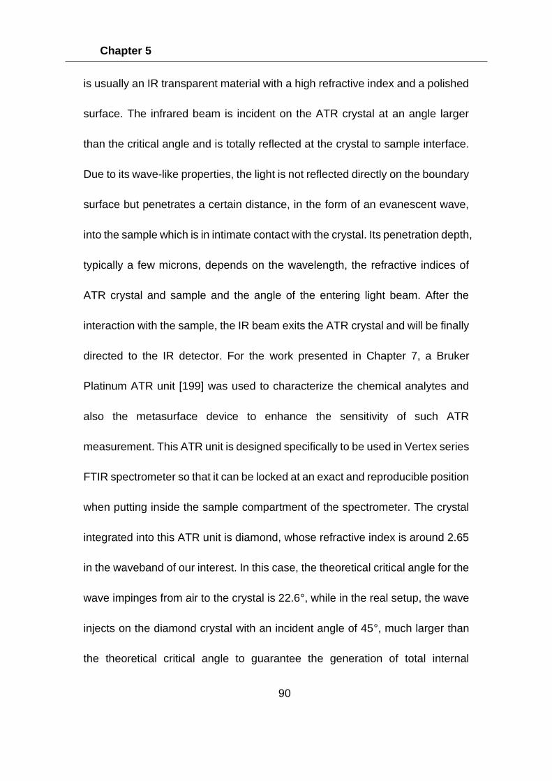
Chapter 5
90
is usually an IR transparent material with a high refractive index and a polished
surface. The infrared beam is incident on the ATR crystal at an angle larger
than the critical angle and is totally reflected at the crystal to sample interface.
Due to its wave-like properties, the light is not reflected directly on the boundary
surface but penetrates a certain distance, in the form of an evanescent wave,
into the sample which is in intimate contact with the crystal. Its penetration depth,
typically a few microns, depends on the wavelength, the refractive indices of
ATR crystal and sample and the angle of the entering light beam. After the
interaction with the sample, the IR beam exits the ATR crystal and will be finally
directed to the IR detector. For the work presented in Chapter 7, a Bruker
Platinum ATR unit [199] was used to characterize the chemical analytes and
also the metasurface device to enhance the sensitivity of such ATR
measurement. This ATR unit is designed specifically to be used in Vertex series
FTIR spectrometer so that it can be locked at an exact and reproducible position
when putting inside the sample compartment of the spectrometer. The crystal
integrated into this ATR unit is diamond, whose refractive index is around 2.65
in the waveband of our interest. In this case, the theoretical critical angle for the
wave impinges from air to the crystal is 22.6°, while in the real setup, the wave
injects on the diamond crystal with an incident angle of 45°, much larger than
the theoretical critical angle to guarantee the generation of total internal
Chapter 5
91
reflection. The wave will only go through one total internal reflection and then
exit to the MCT detector located in the detector compartment. The analytes of
the ATR measurement can either be dripped on the surface if they are liquid or
be pushed firmly on the crystal surface by lowering the lever if the samples are
in solid form.
Figure 5.8 (a) Bruker Platinum ATR module (illustration taken from [199])
(b) Schematic diagram of the mechanism of ATR measurement.
Figure 5.8
Chapter 5
92
Conclusion
To summarize, for the metrology, AFM is mainly used to extract the
thickness information from the samples while SEM is widely used in our
experiment to check the fabrication tolerance of the samples. The fabricated
samples, which were found within the design tolerance, were then
characterized in the FTIR. Several setups were built up to extend the
capabilities of FTIR spectroscopy. With the assistance of these setups, we were
able to obtain reliable transmission, reflection, emission and ATR spectrum
results for the study of mid-infrared devices.
Chapter 6
93
6 Metamaterial-based Graphene Thermal Emitter
6.1 Introduction
Efficient sources of light are a critical component of optical systems.
Especially in the mid-infrared wave band which ranges from 3-12 µm, there
is a continuing need for the development of new sources for low cost portable
mid-infrared gas sensors for applications such as emission detection, and
gas monitoring. There are two main streams in the research of emitting
devices operating in the mid-infrared frequency band: thermal emitters [200-
202], which include conventional incandescent bulbs [203], membrane
filaments and photonic sources, like lasers [204] or light-emitting diodes
(LEDs) [205,206]. Although conventional incandescent sources have a larger
output power and are easier to fabricate, their performance is restrained by a
number of drawbacks including slow response time and limited lifetimes due
to the fragility of the source. In addition, they are usually enclosed in a glass
bulb with inert gas, which limits the emission wavelength range due to the
spectrum will be cut off by thick glass from 3.5 µm [16]. Improvements on the
incandescent sources, like thin membrane emitters, can be essentially
regarded as thin film versions of the conventional incandescent sources. As
Chapter 6
94
the thermal mass of the filament is decreased, this complementary metal-
oxide-semiconductor (CMOS) compatible design offers a slightly faster
responding time compared to incandescent bulbs, leads to higher modulation
frequency ranging from 20-100 Hz [201,202,207], but still not fast enough to
monitor the biological events in situ and in real time. In contrast,
semiconductor LEDs can respond in a much faster speed, normally in
nanosecond scale, often limited by the delay in a driven circuit, which makes
it a natural route for the replacement of these sources. However mid-infrared
LEDs also suffers from relatively poor internal and external quantum
efficiencies [208] due to the narrow bandgap required to achieve emission at
the relatively long wavelengths for sensing gases such as NOx. Furthermore,
sophisticated material growth and extreme growth temperatures [209]
increase not only the difficulty but also the cost of fabrication.
Graphene, two-dimensional graphite, has some unique properties as
atomic thickness [210], excellent electrical conductivity [211], superior
strength [139], and thermal stability [212], which qualify it as an attractive
candidate for the use as an emission source. On one hand, the atomic
thickness of graphene made it much thinner than any other micro-machined
thin membrane. Thus it can achieve an extremely low thermal capacitance
and high modulation frequency [175]. Besides, it can also achieve a higher
Chapter 6
95
radiation power than those quantum emitters. All those made graphene
thermal emitter to be the promising source in the mid-infrared range. The
previous work of my group has shown that the encapsulated graphene
emitter architecture allows sustained operation of the devices in the air, and
that there is measurable modulation of the emission up to a drive frequency
of 100 kHz [19], which is capable of achieving a responding time in sub-
milliseconds. Although graphene thermal emitters seem to be favourable
alternatives to those conventional incandescent emitters, its emission
spectrum is broadband due to the thermal radiation mechanism defined by
Planck’s law. In reality, researchers are more interested in the emission at
specific wavelength than over a broad wavelength range. For example, in
order to measure the concentration of CO2 gas precisely, we only need to
detect its main fingerprint absorption peak at 4.2 µm, the signal-noise ratio
(SNR) and conversion efficiency could be improved by removing any other
wavelength that is out of interest.
In this chapter, we demonstrate the feasibility of patterning a layer of
ultrathin metasurface design on top of a multilayer graphene filament
encapsulated by multilayer hexagonal boron nitride (h-BN) in order to achieve
the narrowband emission spectrum. We also show that even a relatively
simple metamaterial consisting of annular ring resonators can be used in this
Chapter 6
96
architecture to engineer the spectral characteristics, with an enhancement in
the thermal emission at the characteristic absorption wavelength of the target
molecule, and at a second wavelength that could be used for a reference
channel. The integration of the metasurface into the h-BN encapsulated
graphene thermal emitter to tailor the spectral characteristics, and the huge
scope for optimization, demonstrates the feasibility of ultimately creating IR
sources that have some of the attractive features of semiconductor LEDs, but
that also could be more sustainable and cost-effective to manufacture.
As the infrared community prefers to describe the spectrum in terms
of wavelength, the unit throughout this chapter will be chosen to wavelength
unless otherwise specified. Wavelength will also be set as the primary axes
for all plots of spectra in this chapter, while secondary axes will be chosen as
frequency, which is the preference of academic scholars, for comparing to
other results in this thesis or others’ papers.
6.2 Design
6.2.1 Single Band Emitter
The randomly polarized wave emitted from the graphene requires the
frequency selective surface (FSS) designed to tailor the broadband grey body
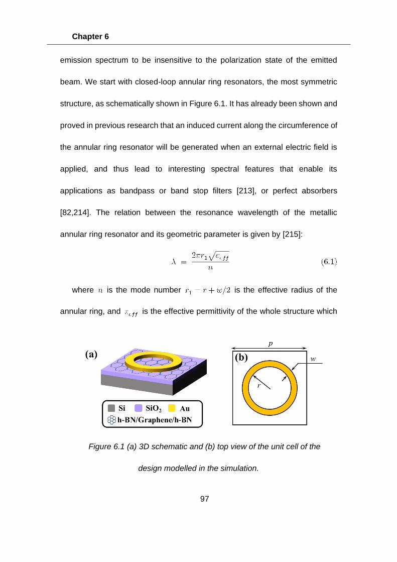
Chapter 6
97
emission spectrum to be insensitive to the polarization state of the emitted
beam. We start with closed-loop annular ring resonators, the most symmetric
structure, as schematically shown in Figure 6.1. It has already been shown and
proved in previous research that an induced current along the circumference of
the annular ring resonator will be generated when an external electric field is
applied, and thus lead to interesting spectral features that enable its
applications as bandpass or band stop filters [213], or perfect absorbers
[82,214]. The relation between the resonance wavelength of the metallic
annular ring resonator and its geometric parameter is given by [215]:
where is the mode number is the effective radius of the
annular ring, and is the effective permittivity of the whole structure which
Figure 6.1 (a) 3D schematic and (b) top view of the unit cell of the
design modelled in the simulation.
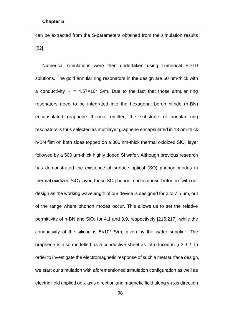
Chapter 6
98
can be extracted from the S-parameters obtained from the simulation results
[62].
Numerical simulations were then undertaken using Lumerical FDTD
solutions. The gold annular ring resonators in the design are 50 nm-thick with
a conductivity = 4.57×10⁷ S/m. Due to the fact that those annular ring
resonators need to be integrated into the hexagonal boron nitride (h-BN)
encapsulated graphene thermal emitter, the substrate of annular ring
resonators is thus selected as multilayer graphene encapsulated in 13 nm-thick
h-BN film on both sides topped on a 300 nm-thick thermal oxidized SiO2 layer
followed by a 500 µm-thick highly doped Si wafer. Although previous research
has demonstrated the existence of surface optical (SO) phonon modes in
thermal oxidized SiO2 layer, those SO phonon modes doesn’t interfere with our
design as the working wavelength of our device is designed for 3 to 7.5 μm, out
of the range where phonon modes occur. This allows us to set the relative
permittivity of h-BN and SiO2 for 4.1 and 3.9, respectively [216,217], while the
conductivity of the silicon is 5×10⁴ S/m, given by the wafer supplier. The
graphene is also modelled as a conductive sheet as introduced in § 2.3.2. In
order to investigate the electromagnetic response of such a metasurface design,
we start our simulation with aforementioned simulation configuration as well as
electric field applied on x-axis direction and magnetic field along y-axis direction
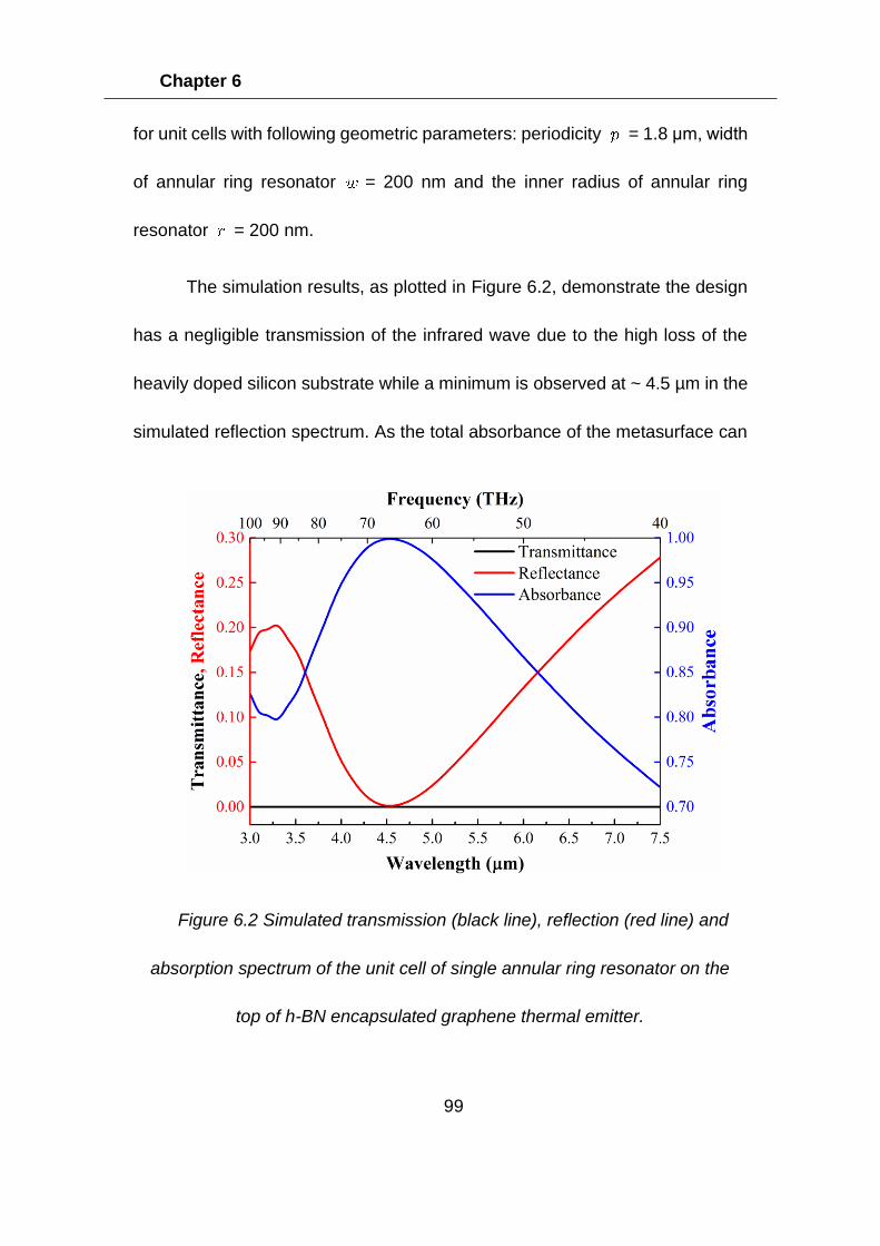
Chapter 6
99
for unit cells with following geometric parameters: periodicity = 1.8 μm, width
of annular ring resonator = 200 nm and the inner radius of annular ring
resonator = 200 nm.
The simulation results, as plotted in Figure 6.2, demonstrate the design
has a negligible transmission of the infrared wave due to the high loss of the
heavily doped silicon substrate while a minimum is observed at ~ 4.5 µm in the
simulated reflection spectrum. As the total absorbance of the metasurface can
Figure 6.2 Simulated transmission (black line), reflection (red line) and
absorption spectrum of the unit cell of single annular ring resonator on the
top of h-BN encapsulated graphene thermal emitter.
Figure 5.7
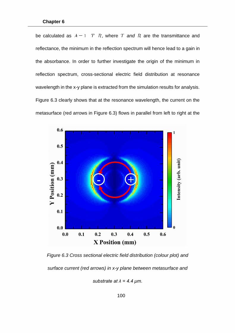
Chapter 6
100
be calculated as , where and are the transmittance and
reflectance, the minimum in the reflection spectrum will hence lead to a gain in
the absorbance. In order to further investigate the origin of the minimum in
reflection spectrum, cross-sectional electric field distribution at resonance
wavelength in the x-y plane is extracted from the simulation results for analysis.
Figure 6.3 clearly shows that at the resonance wavelength, the current on the
metasurface (red arrows in Figure 6.3) flows in parallel from left to right at the
Figure 6.3 Cross sectional electric field distribution (colour plot) and
surface current (red arrows) in x-y plane between metasurface and
substrate at λ = 4.4 µm.
Figure 5.7
Chapter 6
101
upside and the bottom side of the annular ring resonator, leading to an electric
dipole mode like electric field distribution. The excitation of this electric dipole
oscillation will trap the energy at resonance wavelength and achieve an
increase in absorbance. As the absorbance of the device is equal to the
radiation emitted from the device at thermodynamic equilibrium according to
the well-known Kirchhoff’s law of thermal emission [218], the mid-infrared
emitter will thus have an emission peak as well at the resonance wavelength.
Figure 6.4 (a) Simulated absorption/emission spectra of single annular ring
resonator unit cell with different radii ranges from 100 nm to 400 nm. (b)
The resonance wavelength of single annular ring resonator as a function of
radius of the annular ring resonator.
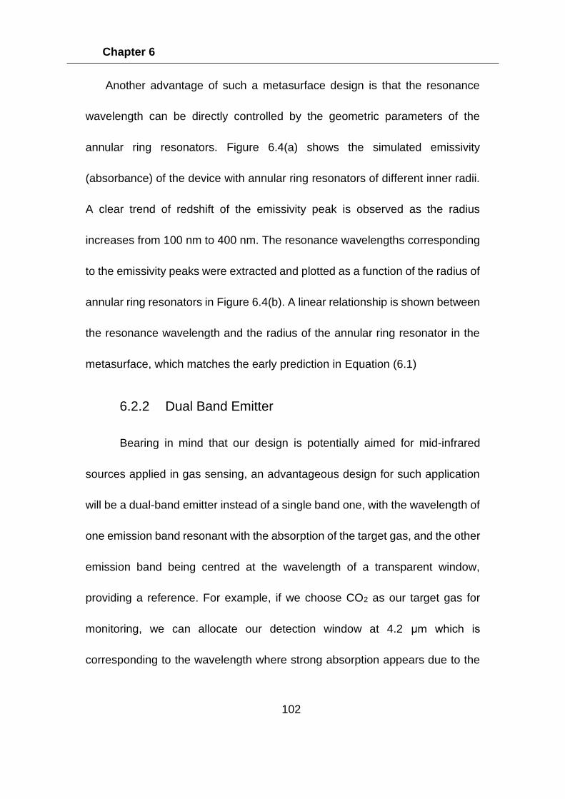
Chapter 6
102
Another advantage of such a metasurface design is that the resonance
wavelength can be directly controlled by the geometric parameters of the
annular ring resonators. Figure 6.4(a) shows the simulated emissivity
(absorbance) of the device with annular ring resonators of different inner radii.
A clear trend of redshift of the emissivity peak is observed as the radius
increases from 100 nm to 400 nm. The resonance wavelengths corresponding
to the emissivity peaks were extracted and plotted as a function of the radius of
annular ring resonators in Figure 6.4(b). A linear relationship is shown between
the resonance wavelength and the radius of the annular ring resonator in the
metasurface, which matches the early prediction in Equation (6.1)
6.2.2 Dual Band Emitter
Bearing in mind that our design is potentially aimed for mid-infrared
sources applied in gas sensing, an advantageous design for such application
will be a dual-band emitter instead of a single band one, with the wavelength of
one emission band resonant with the absorption of the target gas, and the other
emission band being centred at the wavelength of a transparent window,
providing a reference. For example, if we choose CO2 as our target gas for
monitoring, we can allocate our detection window at 4.2 μm which is
corresponding to the wavelength where strong absorption appears due to the
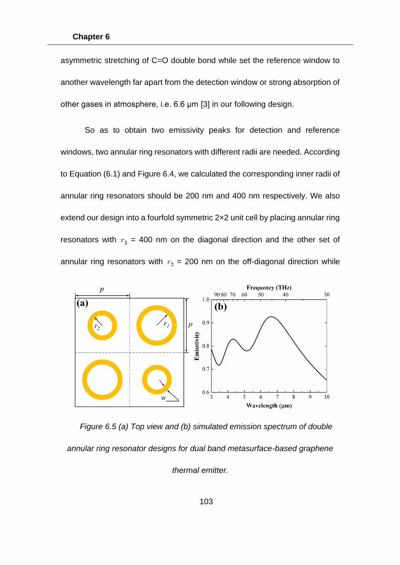
Chapter 6
103
asymmetric stretching of C=O double bond while set the reference window to
another wavelength far apart from the detection window or strong absorption of
other gases in atmosphere, i.e. 6.6 μm [3] in our following design.
So as to obtain two emissivity peaks for detection and reference
windows, two annular ring resonators with different radii are needed. According
to Equation (6.1) and Figure 6.4, we calculated the corresponding inner radii of
annular ring resonators should be 200 nm and 400 nm respectively. We also
extend our design into a fourfold symmetric 2×2 unit cell by placing annular ring
resonators with = 400 nm on the diagonal direction and the other set of
annular ring resonators with = 200 nm on the off-diagonal direction while
Figure 6.5 (a) Top view and (b) simulated emission spectrum of double
annular ring resonator designs for dual band metasurface-based graphene
thermal emitter.
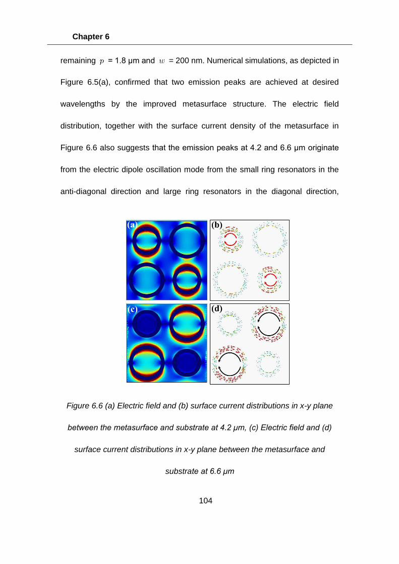
Chapter 6
104
remaining = 1.8 μm and = 200 nm. Numerical simulations, as depicted in
Figure 6.5(a), confirmed that two emission peaks are achieved at desired
wavelengths by the improved metasurface structure. The electric field
distribution, together with the surface current density of the metasurface in
Figure 6.6 also suggests that the emission peaks at 4.2 and 6.6 μm originate
from the electric dipole oscillation mode from the small ring resonators in the
anti-diagonal direction and large ring resonators in the diagonal direction,
Figure 6.6 (a) Electric field and (b) surface current distributions in x-y plane
between the metasurface and substrate at 4.2 μm, (c) Electric field and (d)
surface current distributions in x-y plane between the metasurface and
substrate at 6.6 μm
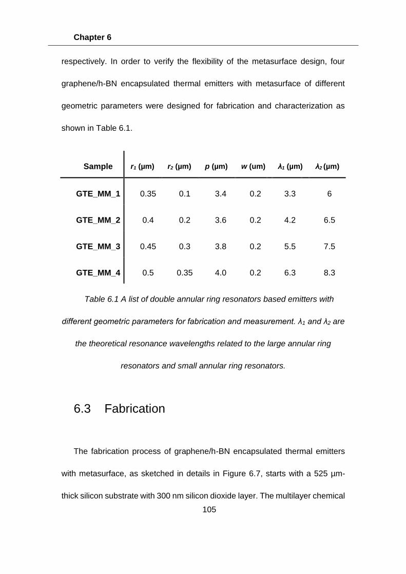
Chapter 6
105
respectively. In order to verify the flexibility of the metasurface design, four
graphene/h-BN encapsulated thermal emitters with metasurface of different
geometric parameters were designed for fabrication and characterization as
shown in Table 6.1.
Table 6.1 A list of double annular ring resonators based emitters with
different geometric parameters for fabrication and measurement. λ1 and λ2 are
the theoretical resonance wavelengths related to the large annular ring
resonators and small annular ring resonators.
6.3 Fabrication
The fabrication process of graphene/h-BN encapsulated thermal emitters
with metasurface, as sketched in details in Figure 6.7, starts with a 525 µm-
thick silicon substrate with 300 nm silicon dioxide layer. The multilayer chemical
Sample r1 (µm) r2 (µm) p (µm) w (um) λ1 (µm) λ2 (µm)
GTE_MM_1 0.35 0.1 3.4 0.2 3.3 6
GTE_MM_2 0.4 0.2 3.6 0.2 4.2 6.5
GTE_MM_3 0.45 0.3 3.8 0.2 5.5 7.5
GTE_MM_4 0.5 0.35 4.0 0.2 6.3 8.3
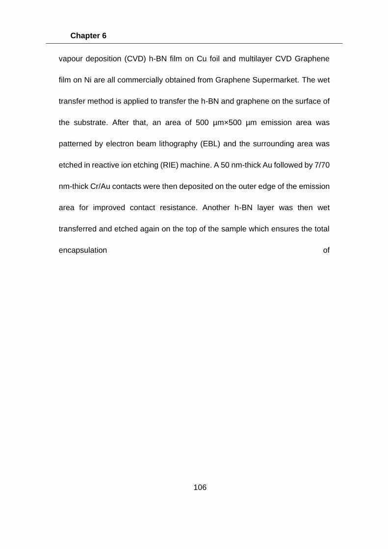
Chapter 6
106
vapour deposition (CVD) h-BN film on Cu foil and multilayer CVD Graphene
film on Ni are all commercially obtained from Graphene Supermarket. The wet
transfer method is applied to transfer the h-BN and graphene on the surface of
the substrate. After that, an area of 500 µm×500 µm emission area was
patterned by electron beam lithography (EBL) and the surrounding area was
etched in reactive ion etching (RIE) machine. A 50 nm-thick Au followed by 7/70
nm-thick Cr/Au contacts were then deposited on the outer edge of the emission
area for improved contact resistance. Another h-BN layer was then wet
transferred and etched again on the top of the sample which ensures the total
encapsulation of
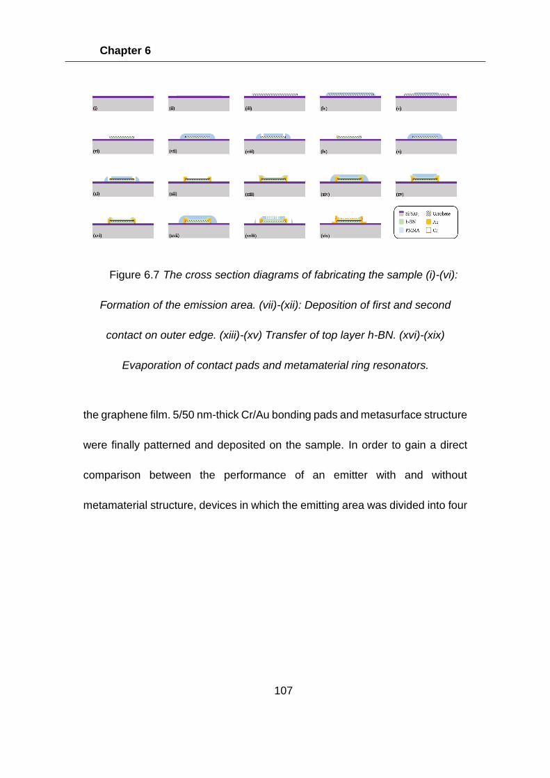
Chapter 6
107
the graphene film. 5/50 nm-thick Cr/Au bonding pads and metasurface structure
were finally patterned and deposited on the sample. In order to gain a direct
comparison between the performance of an emitter with and without
metamaterial structure, devices in which the emitting area was divided into four
Figure 6.7 The cross section diagrams of fabricating the sample (i)-(vi):
Formation of the emission area. (vii)-(xii): Deposition of first and second
contact on outer edge. (xiii)-(xv) Transfer of top layer h-BN. (xvi)-(xix)
Evaporation of contact pads and metamaterial ring resonators.
Chapter 6
108
250 μm × 250 μm quadrants were fabricated, as shown in Figure 6.8. The two
quadrants in the diagonal direction were patterned with metasurface while the
two quadrants in the anti-diagonal direction had no metasurface structure as a
reference.
Figure 6.8 (a) Top view of the schematic illustration of graphene
narrowband thermal emitter with quadrants. (b) Microscope image taken at
50× magnification of the top of the emitter. (c) AFM image taken from
within the red dash box shown in (b).
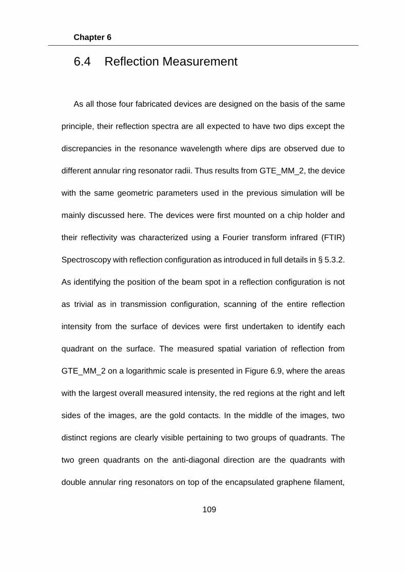
Chapter 6
109
6.4 Reflection Measurement
As all those four fabricated devices are designed on the basis of the same
principle, their reflection spectra are all expected to have two dips except the
discrepancies in the resonance wavelength where dips are observed due to
different annular ring resonator radii. Thus results from GTE_MM_2, the device
with the same geometric parameters used in the previous simulation will be
mainly discussed here. The devices were first mounted on a chip holder and
their reflectivity was characterized using a Fourier transform infrared (FTIR)
Spectroscopy with reflection configuration as introduced in full details in § 5.3.2.
As identifying the position of the beam spot in a reflection configuration is not
as trivial as in transmission configuration, scanning of the entire reflection
intensity from the surface of devices were first undertaken to identify each
quadrant on the surface. The measured spatial variation of reflection from
GTE_MM_2 on a logarithmic scale is presented in Figure 6.9, where the areas
with the largest overall measured intensity, the red regions at the right and left
sides of the images, are the gold contacts. In the middle of the images, two
distinct regions are clearly visible pertaining to two groups of quadrants. The
two green quadrants on the anti-diagonal direction are the quadrants with
double annular ring resonators on top of the encapsulated graphene filament,
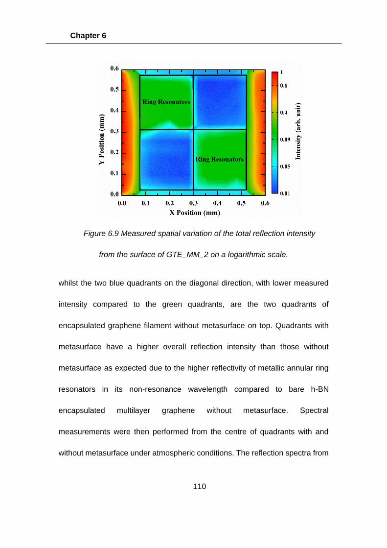
Chapter 6
110
whilst the two blue quadrants on the diagonal direction, with lower measured
intensity compared to the green quadrants, are the two quadrants of
encapsulated graphene filament without metasurface on top. Quadrants with
metasurface have a higher overall reflection intensity than those without
metasurface as expected due to the higher reflectivity of metallic annular ring
resonators in its non-resonance wavelength compared to bare h-BN
encapsulated multilayer graphene without metasurface. Spectral
measurements were then performed from the centre of quadrants with and
without metasurface under atmospheric conditions. The reflection spectra from
Figure 6.9 Measured spatial variation of the total reflection intensity
from the surface of GTE_MM_2 on a logarithmic scale.
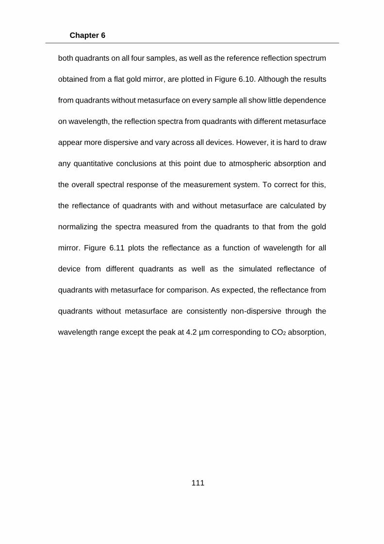
Chapter 6
111
both quadrants on all four samples, as well as the reference reflection spectrum
obtained from a flat gold mirror, are plotted in Figure 6.10. Although the results
from quadrants without metasurface on every sample all show little dependence
on wavelength, the reflection spectra from quadrants with different metasurface
appear more dispersive and vary across all devices. However, it is hard to draw
any quantitative conclusions at this point due to atmospheric absorption and
the overall spectral response of the measurement system. To correct for this,
the reflectance of quadrants with and without metasurface are calculated by
normalizing the spectra measured from the quadrants to that from the gold
mirror. Figure 6.11 plots the reflectance as a function of wavelength for all
device from different quadrants as well as the simulated reflectance of
quadrants with metasurface for comparison. As expected, the reflectance from
quadrants without metasurface are consistently non-dispersive through the
wavelength range except the peak at 4.2 µm corresponding to CO2 absorption,
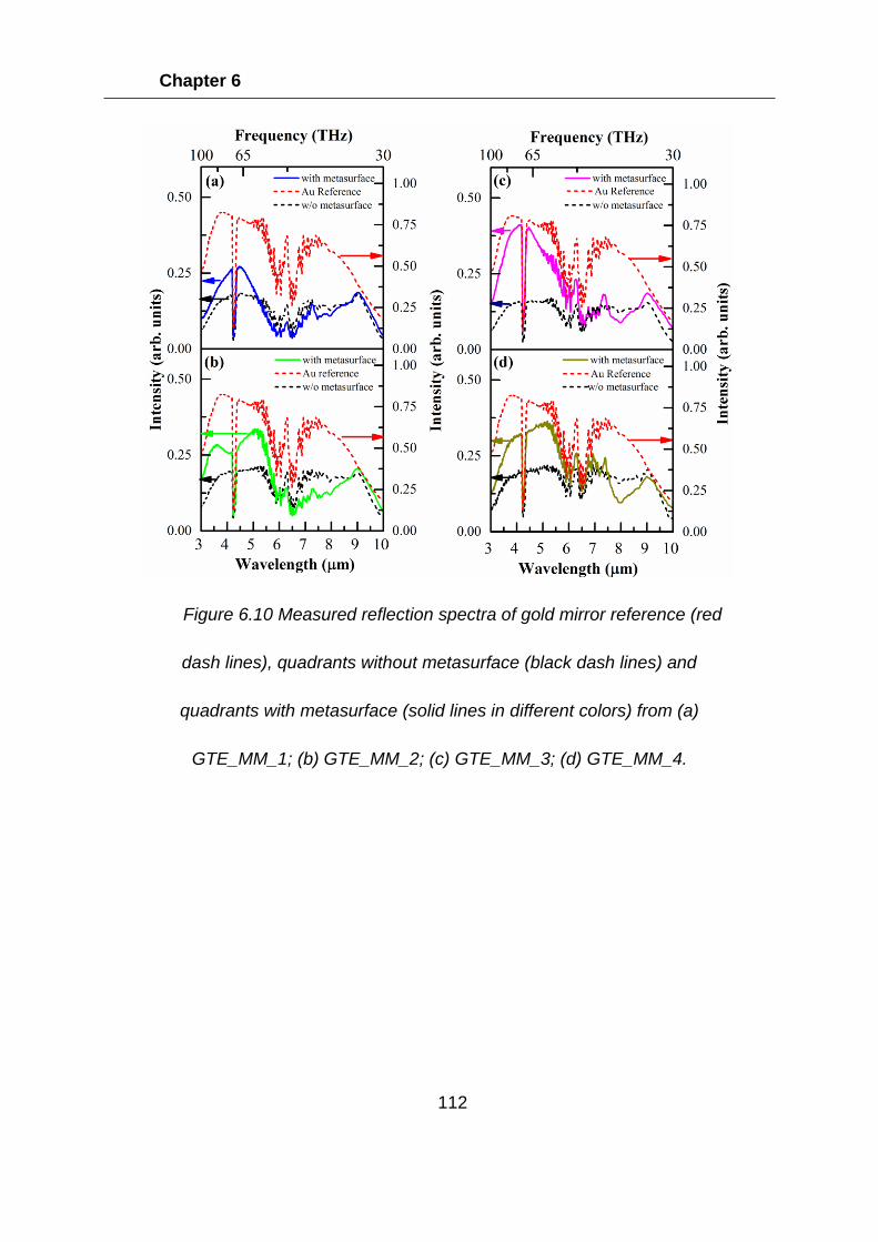
Chapter 6
112
Figure 6.10 Measured reflection spectra of gold mirror reference (red
dash lines), quadrants without metasurface (black dash lines) and
quadrants with metasurface (solid lines in different colors) from (a)
GTE_MM_1; (b) GTE_MM_2; (c) GTE_MM_3; (d) GTE_MM_4.
Chapter 6
113
7 and 9 µm due to the phonon mode of the underlying h-BN film and SiO2 layer,
respectively [160,219]. However, the reflectance spectra from quadrants with
metasurface show a strong wavelength dependence. A two main reflection
minima feature, ‘W’ shaped spectral response, can be observed in all four
Figure 6.11 Normalized (red solid lines) and simulated (blue solid lines)
reflectance of the quadrants with metasurface and normalized reflectance
(black dash lines) of quadrants without metasurface from (a) GTE_MM_1,
(b) GTE_MM_2, (c) GTE_MM_3, (d) GTE_MM_4.
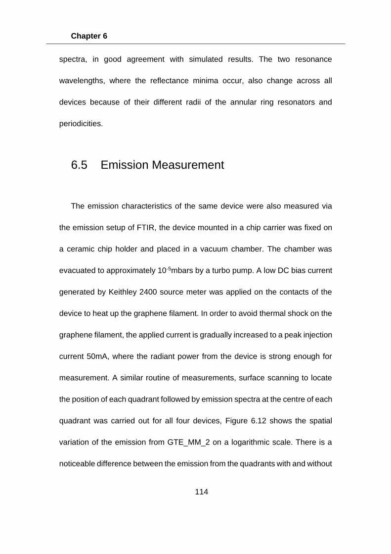
Chapter 6
114
spectra, in good agreement with simulated results. The two resonance
wavelengths, where the reflectance minima occur, also change across all
devices because of their different radii of the annular ring resonators and
periodicities.
6.5 Emission Measurement
The emission characteristics of the same device were also measured via
the emission setup of FTIR, the device mounted in a chip carrier was fixed on
a ceramic chip holder and placed in a vacuum chamber. The chamber was
evacuated to approximately 10-5mbars by a turbo pump. A low DC bias current
generated by Keithley 2400 source meter was applied on the contacts of the
device to heat up the graphene filament. In order to avoid thermal shock on the
graphene filament, the applied current is gradually increased to a peak injection
current 50mA, where the radiant power from the device is strong enough for
measurement. A similar routine of measurements, surface scanning to locate
the position of each quadrant followed by emission spectra at the centre of each
quadrant was carried out for all four devices, Figure 6.12 shows the spatial
variation of the emission from GTE_MM_2 on a logarithmic scale. There is a
noticeable difference between the emission from the quadrants with and without
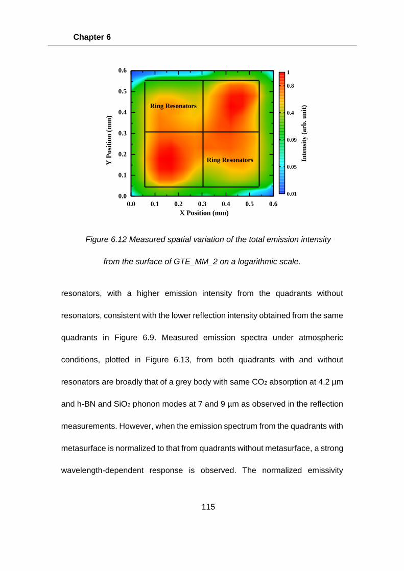
Chapter 6
115
resonators, with a higher emission intensity from the quadrants without
resonators, consistent with the lower reflection intensity obtained from the same
quadrants in Figure 6.9. Measured emission spectra under atmospheric
conditions, plotted in Figure 6.13, from both quadrants with and without
resonators are broadly that of a grey body with same CO2 absorption at 4.2 µm
and h-BN and SiO2 phonon modes at 7 and 9 µm as observed in the reflection
measurements. However, when the emission spectrum from the quadrants with
metasurface is normalized to that from quadrants without metasurface, a strong
wavelength-dependent response is observed. The normalized emissivity
0.0 0.1 0.2 0.3 0.4 0.5 0.6
0.0
0.1
0.2
0.3
0.4
0.5
0.6
Inte
nsi
ty (
arb
. u
nit
)
0.01
0.05
0.09
0.4
0.8
1
Ring Resonators
Ring ResonatorsY
Posi
tion
(m
m)
X Position (mm)
Figure 6.12 Measured spatial variation of the total emission intensity
from the surface of GTE_MM_2 on a logarithmic scale.
A
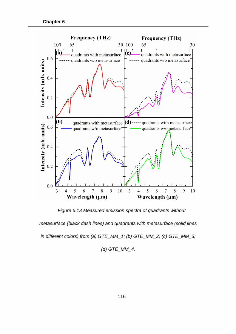
Chapter 6
116
Figure 6.13 Measured emission spectra of quadrants without
metasurface (black dash lines) and quadrants with metasurface (solid lines
in different colors) from (a) GTE_MM_1; (b) GTE_MM_2; (c) GTE_MM_3;
(d) GTE_MM_4.
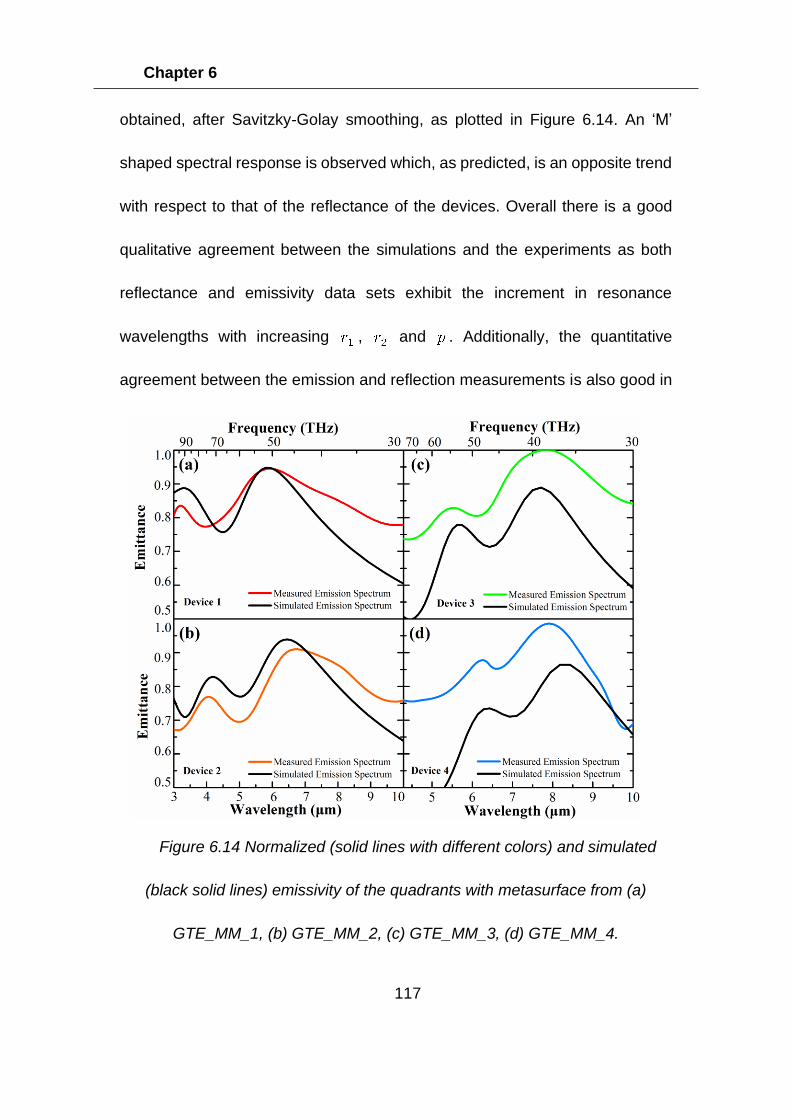
Chapter 6
117
obtained, after Savitzky-Golay smoothing, as plotted in Figure 6.14. An ‘M’
shaped spectral response is observed which, as predicted, is an opposite trend
with respect to that of the reflectance of the devices. Overall there is a good
qualitative agreement between the simulations and the experiments as both
reflectance and emissivity data sets exhibit the increment in resonance
wavelengths with increasing , and . Additionally, the quantitative
agreement between the emission and reflection measurements is also good in
Figure 6.14 Normalized (solid lines with different colors) and simulated
(black solid lines) emissivity of the quadrants with metasurface from (a)
GTE_MM_1, (b) GTE_MM_2, (c) GTE_MM_3, (d) GTE_MM_4.
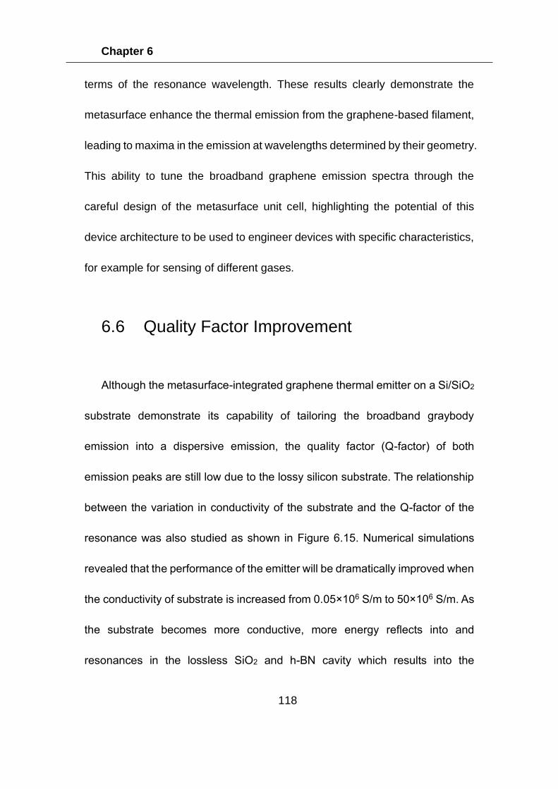
Chapter 6
118
terms of the resonance wavelength. These results clearly demonstrate the
metasurface enhance the thermal emission from the graphene-based filament,
leading to maxima in the emission at wavelengths determined by their geometry.
This ability to tune the broadband graphene emission spectra through the
careful design of the metasurface unit cell, highlighting the potential of this
device architecture to be used to engineer devices with specific characteristics,
for example for sensing of different gases.
6.6 Quality Factor Improvement
Although the metasurface-integrated graphene thermal emitter on a Si/SiO2
substrate demonstrate its capability of tailoring the broadband graybody
emission into a dispersive emission, the quality factor (Q-factor) of both
emission peaks are still low due to the lossy silicon substrate. The relationship
between the variation in conductivity of the substrate and the Q-factor of the
resonance was also studied as shown in Figure 6.15. Numerical simulations
revealed that the performance of the emitter will be dramatically improved when
the conductivity of substrate is increased from 0.05×10⁶ S/m to 50×106 S/m. As
the substrate becomes more conductive, more energy reflects into and
resonances in the lossless SiO2 and h-BN cavity which results into the
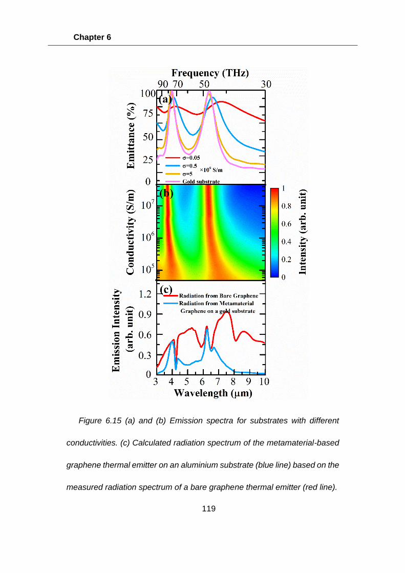
Chapter 6
119
Figure 6.15 (a) and (b) Emission spectra for substrates with different
conductivities. (c) Calculated radiation spectrum of the metamaterial-based
graphene thermal emitter on an aluminium substrate (blue line) based on the
measured radiation spectrum of a bare graphene thermal emitter (red line).
Chapter 6
120
increasing decay rate of the emission peak. As a result, the amplitude together
with the Q-factor of the emission peaks will be logarithmically increased. This
feature results from the fact that the resonance of the metasurface at resonance
wavelength will constructively interfere with the thermal radiation and
consequently enhance the emission energy. As the silicon used in the
fabrication is already the highest doped silicon wafer can be purchased from
the commercial market, the Si/SiO2 substrate needs to be replaced by an
aluminium substrate on which a 300 nm-thick SiO2 was ion beam sputtered as
a spacer layer in order to increase the Q-factor from 6.5 to 13 (Figure 6.16).
Figure 6.16 Calculated Q-factors of both emission peaks (blue line for 1st
emission peak and red line for 2nd emission peak) for substrates with
different conductivities.
Chapter 6
121
6.7 Summary
In summary, a metasurface composed of annular ring resonator is first
investigated for tailoring the randomly polarized, broadband emission from h-
BN encapsulated graphene filament into a narrower bandwidth. Numerical
simulations present that the electric dipole oscillation of the annular ring
resonator can lead to an emission peak at a specific resonance wavelength.
The annular ring resonator design is then extended to a fourfold 2×2 unit cell
with a set of large annular ring resonators on diagonal direction and the other
set of small annular ring resonators on anti-diagonal direction for the purpose
of building up a gas sensor with dual emission peak, one interacting with the
target gas while the other one providing the reference. Four emitters with such
metasurface of different geometric parameters were designed for emission
peaks located at various points between 3 - 8.5 µm. The initial measurements
performed on the fabricated emitters were FTIR reflection measurements.
Distinct overall spatial variations of total reflection intensity can be observed
between the quadrants with and without metasurface. Normalized reflection
spectra also demonstrate that all four devices exhibit a ‘W’ shaped spectral
response at different resonance wavelengths due to the different radii and
periodicities of the design, as we predicted. Similarly, when the devices are
Chapter 6
122
driven by DC current, the emission measurement under FTIR with emission
configuration also shows distinguishable total emission intensities from
quadrants with and without metasurface. The normalized emission spectra all
exhibit a dual-peak ‘M’ shaped spectra response as desired. Both the
normalized reflection and emission spectra of four devices also show the
resonance wavelengths increase with the increment in the radii of annular ring
resonators, , and periodicity , all agree well with the simulated results,
which can be concluded that such dual annular ring resonators metasurface
design can be utilised to predictably tune the graphene emission spectrum.
Finally, simulations show that the addition of a conducting layer below the SiO2
layer can greatly increase the Q-factor of the resonance features in the
emission spectrum. The possibility of tailoring the emission characteristics of
these devices, which can reduce manufacturing costs and allow for modulation
at relatively high frequencies, demonstrates their potential for use in
applications such as infrared gas sensing.
Chapter 7
123
7 Wave Trapping Sensor for Attenuated Total
Reflection Spectroscopy
Introduction
As highlighted in previous chapters, the infrared region of the spectrum is
highly attractive due to its use in providing a powerful, label-free, non-
destructive analytical technique to identify chemicals [2,7,220]. The mid-
infrared photon, whose energy ranges from 0.06 to 0.4eV, can be absorbed by
the unique vibrational mode of specific chemical bonds. Since different bonds,
or the same bond with different vibrational modes have their own unique
infrared absorption spectra, known as the molecular fingerprint, corresponding
to the photon energy they require to excite their vibrational transitions, this
enables us to analyse the compound in the chemical by simply observing the
spectrum obtained from an infrared spectroscopy. However, conventional
infrared spectroscopies have two main drawbacks. Firstly, the interaction
between the mid-infrared wave and molecule is weak due to the size mismatch.
The spot size of the infrared wave is in the size of tens or hundreds of microns
far bigger than the scale of atoms. So the spectroscopic measurement on trace
amounts of analytes remains an intractable challenge [221]. Secondly, due to
Chapter 7
124
the native aqueous environment of many analytes under test, the strong
absorption of water will severely interfere with the measurements on the
absorption of target molecules. Hence additional sample preparations, such as
drying the samples or applying the samples in the form of a thin film with the
same thickness [222], are required for the measurements which makes it
unrealistic to characterize those samples in real time.
Attenuated total reflection (ATR) infrared spectroscopy, as introduced in
Chapter 5.3, can be viewed as an improvement on the conventional infrared
spectroscopy, to some extent overcomes both aforementioned disadvantages.
Under ATR condition, the evanescent wave generated through total internal
reflection mechanism interacts with the analytes will be confined within a
distance, which is on the order of the wavelength, from the interface [223]. This
dramatically reduces the detection volume of infrared radiation, which is
normally the spot size in conventional infrared spectroscopy cases, and thus
results in an enhanced light-matter interaction. Meanwhile, the water absorption
is also suppressed under ATR condition which also allows straightforward
analyses on samples in its aqueous form, without specific sample preparation
[224,225]. Although the ATR approach has improved the capability of achieving
qualitative measurement in situ, the relatively weak interaction between the
infrared radiation and the analytes limits the sensitivity for quantitative analysis.
Chapter 7
125
In order to make the light-matter interaction stronger, the evanescent wave
needs to be confined in a subwavelength volume with minimal energy loss.
Metasurfaces, once again turns out to be the solution as they offer high flexibility
in controlling the propagation of surface waves and the resultant field
distributions [226,227]. Pioneering research on such metasurface structure as
aggregates [228], arrays [158], and nano-antennas [229,230] have already
demonstrated the enhancement in absorption at the resonance frequency
under conventional transmission or reflection setup. The localization of the
collective oscillations of electrons at the surface enables those designs to
confine the wave in a subwavelength scale area without significant energy loss.
In this chapter, an equivalent model was built to simulate the
electromagnetic response of the device tested under ATR configuration. Based
on that model, a metasurface design was proposed to enhance the interaction
between the evanescent wave in mid-infrared and different trace chemical
analytes. Different substrates, Si and Si/SiO2 were used as substrates in
fabrication to determine whether the phonon mode in SiO2 will further improve
the detection sensitivity.
From the result obtained, we show that a metasurface can be used to
relatively easily increase the sensitivity of infrared attenuated total reflection
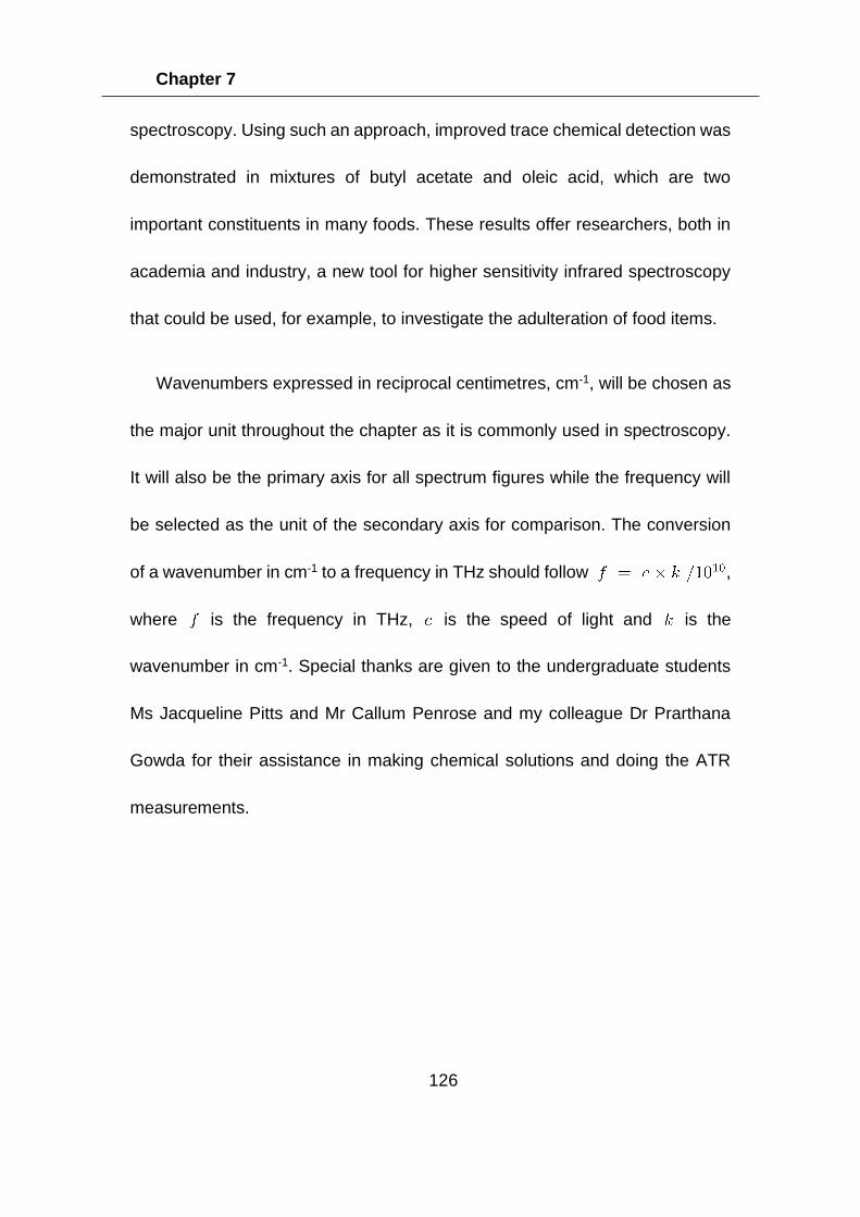
Chapter 7
126
spectroscopy. Using such an approach, improved trace chemical detection was
demonstrated in mixtures of butyl acetate and oleic acid, which are two
important constituents in many foods. These results offer researchers, both in
academia and industry, a new tool for higher sensitivity infrared spectroscopy
that could be used, for example, to investigate the adulteration of food items.
Wavenumbers expressed in reciprocal centimetres, cm-1, will be chosen as
the major unit throughout the chapter as it is commonly used in spectroscopy.
It will also be the primary axis for all spectrum figures while the frequency will
be selected as the unit of the secondary axis for comparison. The conversion
of a wavenumber in cm-1 to a frequency in THz should follow ,
where is the frequency in THz, is the speed of light and is the
wavenumber in cm-1. Special thanks are given to the undergraduate students
Ms Jacqueline Pitts and Mr Callum Penrose and my colleague Dr Prarthana
Gowda for their assistance in making chemical solutions and doing the ATR
measurements.
Chapter 7
127
Modelling
Modelling of ATR configuration
It is clear that under the ATR configuration, it is the evanescent wave
generated by the total internal reflection mechanism that interacts with the
analytes. As a result, in order to investigate the responses of the device and
Figure 7.1 (a) 3D schematic of the simulation model used to generate
evanescent wave with incident wave propagates along z-axis with an angle
of incidence θ and electric field polarized along x-axis. (b)The electric field
distribution in x-z plane at k = 1000 cm-1 with incident angle = 10° (left) and
45° (right).
Chapter 7
128
analytes in an ATR setup, the evanescent wave is required to be used as the
source in our simulation. Unfortunately, few commercial software packages can
directly choose evanescent wave as the source for simulation. Here a
simulation model, which is equivalent to the ATR setup used in our experiment
as shown in Figure 5.8, is introduced for the purpose of generating the
evanescent wave. The simulation model as schematically shown in Figure 7.1,
generates the evanescent wave by total internal reflection through injecting an
oblique incident wave on the diamond ATR crystal towards the air. The area
highlighted in red is the source port, which generates an oblique
electromagnetic wave along the blue arrow direction. The green arrow in the
schematic shows the polarization of the wave. In addition, the refractive index
of the diamond crystal is set to 2.64, same refractive index as the ATR crystal
used in the measurement according to the manual and periodic boundary
conditions are applied on all x-z and y-z boundaries. Here restricted by the
shortage of FDTD method in simulation oblique source, FEM-based software
COMSOL Multiphysics was used for all the simulation work in this chapter, as
it performs much better in the case of simulating oblique incident wave with a
broad frequency range. The electric field distributions in Figure 7.1(b) suggest
that when the angle of incidence is low, wave beam can still penetrate into
air through refraction while when increases, for instance = 45° as the
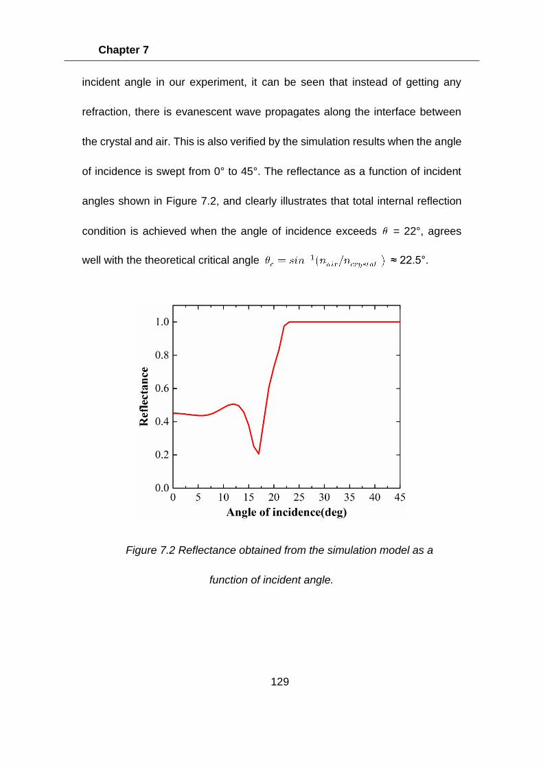
Chapter 7
129
incident angle in our experiment, it can be seen that instead of getting any
refraction, there is evanescent wave propagates along the interface between
the crystal and air. This is also verified by the simulation results when the angle
of incidence is swept from 0° to 45°. The reflectance as a function of incident
angles shown in Figure 7.2, and clearly illustrates that total internal reflection
condition is achieved when the angle of incidence exceeds = 22°, agrees
well with the theoretical critical angle ≈ 22.5°.
Figure 7.2 Reflectance obtained from the simulation model as a
function of incident angle.
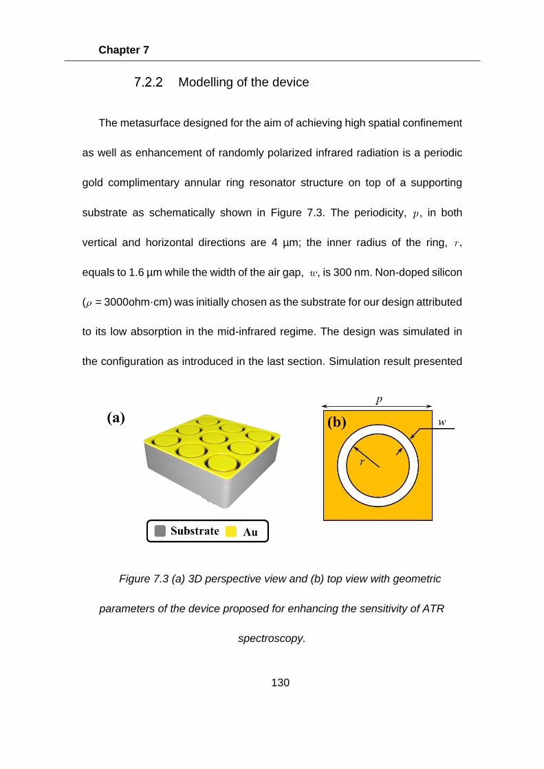
Chapter 7
130
Modelling of the device
The metasurface designed for the aim of achieving high spatial confinement
as well as enhancement of randomly polarized infrared radiation is a periodic
gold complimentary annular ring resonator structure on top of a supporting
substrate as schematically shown in Figure 7.3. The periodicity, , in both
vertical and horizontal directions are 4 µm; the inner radius of the ring,
equals to 1.6 µm while the width of the air gap, , is 300 nm. Non-doped silicon
( = 3000ohm·cm) was initially chosen as the substrate for our design attributed
to its low absorption in the mid-infrared regime. The design was simulated in
the configuration as introduced in the last section. Simulation result presented
Figure 7.3 (a) 3D perspective view and (b) top view with geometric
parameters of the device proposed for enhancing the sensitivity of ATR
spectroscopy.
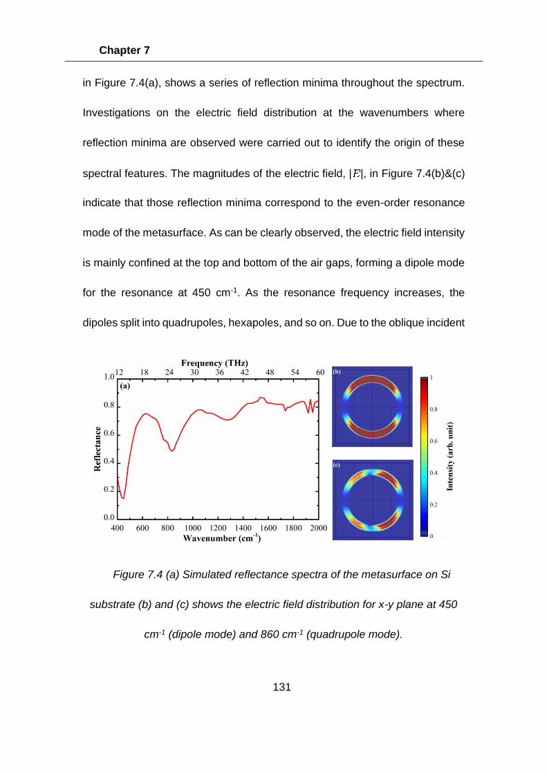
Chapter 7
131
in Figure 7.4(a), shows a series of reflection minima throughout the spectrum.
Investigations on the electric field distribution at the wavenumbers where
reflection minima are observed were carried out to identify the origin of these
spectral features. The magnitudes of the electric field, | |, in Figure 7.4(b)&(c)
indicate that those reflection minima correspond to the even-order resonance
mode of the metasurface. As can be clearly observed, the electric field intensity
is mainly confined at the top and bottom of the air gaps, forming a dipole mode
for the resonance at 450 cm-1. As the resonance frequency increases, the
dipoles split into quadrupoles, hexapoles, and so on. Due to the oblique incident
Figure 7.4 (a) Simulated reflectance spectra of the metasurface on Si
substrate (b) and (c) shows the electric field distribution for x-y plane at 450
cm-1 (dipole mode) and 860 cm-1 (quadrupole mode).
Chapter 7
132
of the electromagnetic wave in the ATR system the resonant modes also
become less symmetric, and weaker in electric field confinement for a higher
order of resonance. Although the confinement of the electric field in the small
gap at its resonance mode is what we expected, the low reflectance at the
resonant frequency which will directly lead to a low SNR and thus poor
sensitivity for the measurement, make it not a good design for ATR system. In
fact, having a good confinement of the energy at the surface of the device and
achieving high reflectance from the device seems to conflict with each other. In
order to overcome this obstacle, the substrate is changed to 300 nm thermal
oxidized SiO2 on top of the non-doped Si wafer. Previous research has proved
the existence of surface optical phonon modes in thermal oxidized SiO2 in the
range of 400 to 1300 cm-1 [160]. By overlapping the resonance modes of
metasurface and the phonon modes of SiO2, these two modes will couple with
each other and the energy trapped in the gap will excite the collective oscillation
of phonons in SiO2. Numerical simulations are conducted to prove the existence
of this hybrid resonance model. The permittivity of SiO2 is modelled by using
the ionic dielectric function of the form:
Chapter 7
133
where is the frequency of the th phonon mode, and their values are taken
to be [464.8, 810.9, 1129.0] cm−1 for three phonon modes ( = 3), following
data obtained from the literature [231,232], providing that is larger
than under any circumstance. is the oscillation strength
of the nth mode, and are taken [0.75, 0.15, 0.60] and = 2.4 is the high-
frequency dielectric constant for the SiO2 substrate. Figure 7.5 shows the
calculated real part and imaginary of the refractive index of SiO2 which agrees
well with previously reported values. Based on this, the dispersion diagram of
the device on Si/SiO2 substrate is also calculated by simulating the device with
different scales, as shown in Figure 7.5. The figure clearly shows the coupling
between the dipole and quadrupole resonance modes of the metasurface and
the SO phonon mode of SiO2 layer at 470 cm-1 and 1084 cm-1. It should be
noted that although SiO2 also has another phonon mode at 810 cm-1, the
oscillation strength of phonon mode is only ¼ of the other two phonon modes,
this makes its coupling with metasurface resonance mode quite weak. The data
can be extracted from the dispersion diagram for the wavevector = 15.8×10³
cm-1, the same parameter as used for simulation of the device on Si substrate
and compare the reflection spectra of both spectra. It can be observed from
Figure 7.6 that despite of the slight blueshift of the resonance frequency caused
by the lower refractive index of the SiO2 layer, there now appears to be two
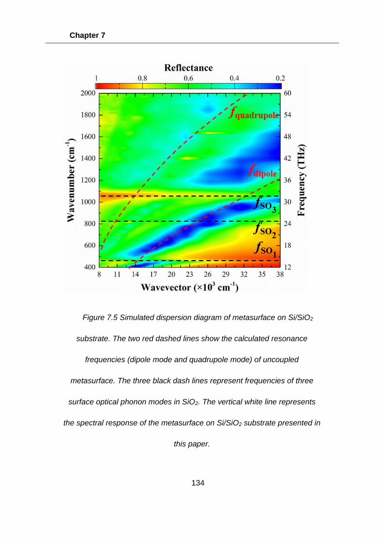
Chapter 7
134
Figure 7.5 Simulated dispersion diagram of metasurface on Si/SiO2
substrate. The two red dashed lines show the calculated resonance
frequencies (dipole mode and quadrupole mode) of uncoupled
metasurface. The three black dash lines represent frequencies of three
surface optical phonon modes in SiO2. The vertical white line represents
the spectral response of the metasurface on Si/SiO2 substrate presented in
this paper.
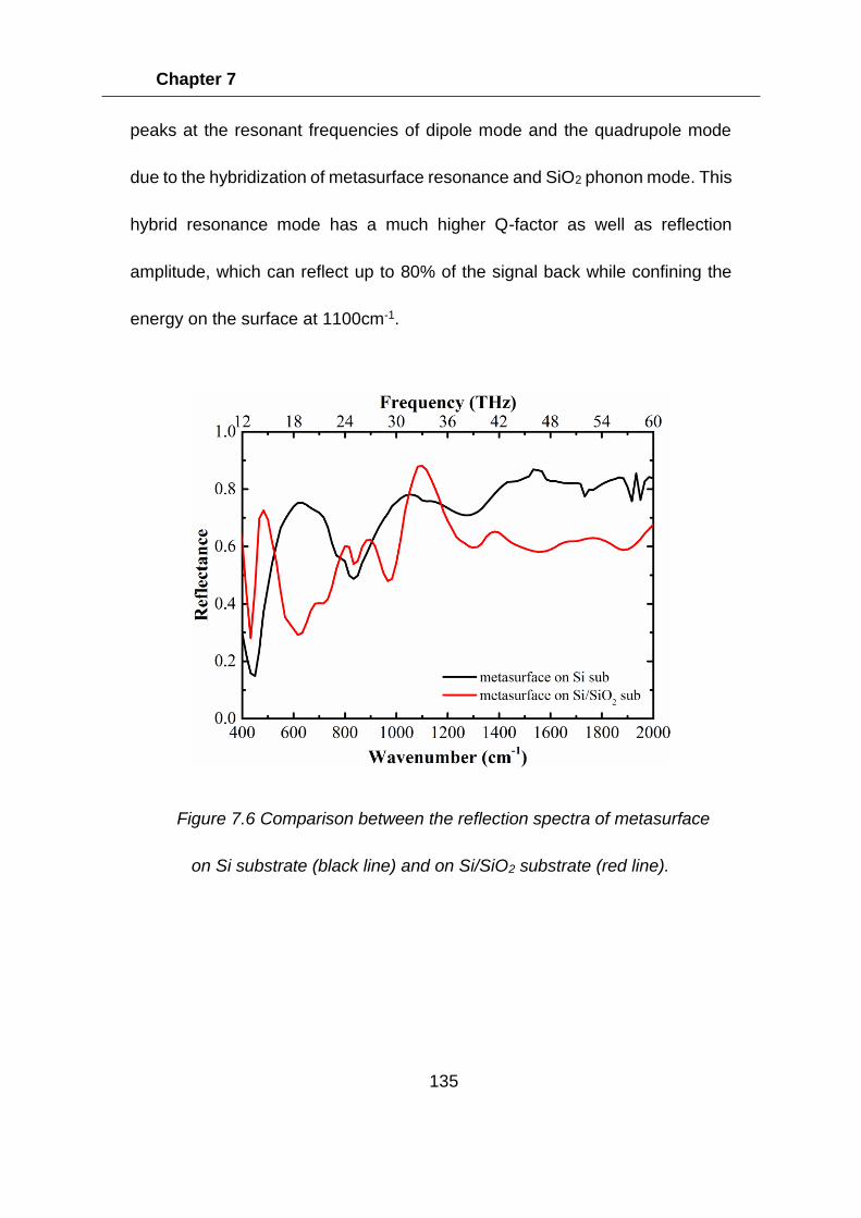
Chapter 7
135
peaks at the resonant frequencies of dipole mode and the quadrupole mode
due to the hybridization of metasurface resonance and SiO2 phonon mode. This
hybrid resonance mode has a much higher Q-factor as well as reflection
amplitude, which can reflect up to 80% of the signal back while confining the
energy on the surface at 1100cm-1.
Figure 7.6 Comparison between the reflection spectra of metasurface
on Si substrate (black line) and on Si/SiO2 substrate (red line).
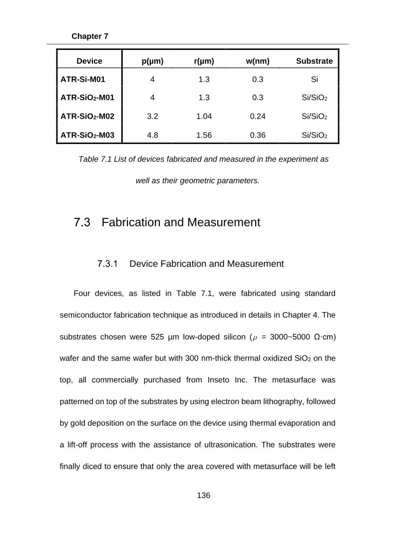
Chapter 7
136
Device
Number
p(µm) r(µm) w(nm) Substrate
ATR-Si-M01 4 1.3 0.3 Si
ATR-SiO2-M01 4 1.3 0.3 Si/SiO2
ATR-SiO2-M02 3.2 1.04 0.24 Si/SiO2
ATR-SiO2-M03 4.8 1.56 0.36 Si/SiO2
Table 7.1 List of devices fabricated and measured in the experiment as
well as their geometric parameters.
Fabrication and Measurement
Device Fabrication and Measurement
Four devices, as listed in Table 7.1, were fabricated using standard
semiconductor fabrication technique as introduced in details in Chapter 4. The
substrates chosen were 525 µm low-doped silicon ( = 3000~5000 Ω·cm)
wafer and the same wafer but with 300 nm-thick thermal oxidized SiO2 on the
top, all commercially purchased from Inseto Inc. The metasurface was
patterned on top of the substrates by using electron beam lithography, followed
by gold deposition on the surface on the device using thermal evaporation and
a lift-off process with the assistance of ultrasonication. The substrates were
finally diced to ensure that only the area covered with metasurface will be left
Chapter 7
137
on the device for testing. Fourier Transform Infrared Spectroscopy (Bruker
Vertex 80v) in conjunction with Attenuated Total Reflection module (Platinum
ATR Accessory) which has been introduced in Chapter 5 was used to
characterize the devices first in the experiment. Spectra were recorded with
8cm-1 wavenumber resolution and 8.0 mm size aperture in the wavenumber
range from 400 to 2000 cm-1 that are averaged over 256 scans per
measurement. All samples were placed on top of the ATR spectrometer with
the metasurface side of the device always facing the ATR crystal and a
pressure application device was pivoted on the sample to ensure the distance
between the ATR crystal and the metasurface is the same throughout the
measurement. Figure 7.7(b) plots the reflectance spectra of the devices with
the same metasurface structure but different substrate (ATR-Si-M01 and ATR-
SiO2-M01). Two minima in the reflection spectra of the metasurface on Si
substrate (ATR-Si-M01) are observed at 450 and 858 cm-1 while two hybrid
resonance modes occur at 476 and 1076 cm-1 instead for metasurface on SiO2
substrate (ATR-SiO2-M01). Measurements are also conducted on metasurface
structure with different size scales on Si/SiO2 substrate (ATR-SiO2-M01, ATR-
SiO2-M02, ATR-SiO2-M03). The reflectance spectra obtained from the
measurement, shown in Figure 7.8(a) reveal that although the resonance of
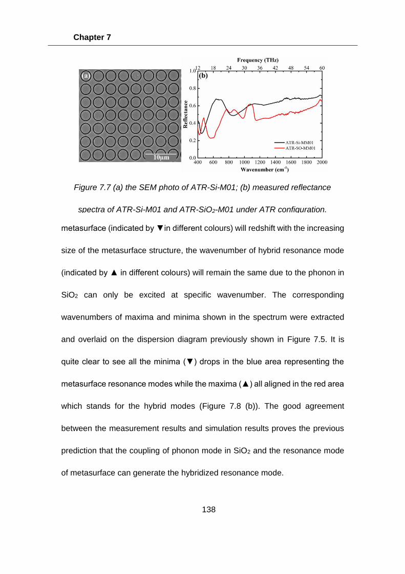
Chapter 7
138
metasurface (indicated by ▼in different colours) will redshift with the increasing
size of the metasurface structure, the wavenumber of hybrid resonance mode
(indicated by ▲ in different colours) will remain the same due to the phonon in
SiO2 can only be excited at specific wavenumber. The corresponding
wavenumbers of maxima and minima shown in the spectrum were extracted
and overlaid on the dispersion diagram previously shown in Figure 7.5. It is
quite clear to see all the minima (▼) drops in the blue area representing the
metasurface resonance modes while the maxima (▲) all aligned in the red area
which stands for the hybrid modes (Figure 7.8 (b)). The good agreement
between the measurement results and simulation results proves the previous
prediction that the coupling of phonon mode in SiO2 and the resonance mode
of metasurface can generate the hybridized resonance mode.
Figure 7.7 (a) the SEM photo of ATR-Si-M01; (b) measured reflectance
spectra of ATR-Si-M01 and ATR-SiO2-M01 under ATR configuration.
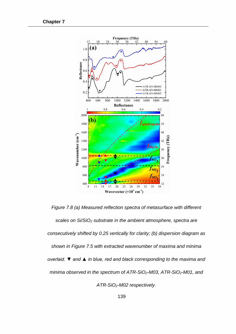
Chapter 7
139
Figure 7.8 (a) Measured reflection spectra of metasurface with different
scales on Si/SiO2 substrate in the ambient atmosphere, spectra are
consecutively shifted by 0.25 vertically for clarity; (b) dispersion diagram as
shown in Figure 7.5 with extracted wavenumber of maxima and minima
overlaid. ▼ and ▲ in blue, red and black corresponding to the maxima and
minima observed in the spectrum of ATR-SiO2-M03, ATR-SiO2-M01, and
ATR-SiO2-M02 respectively.
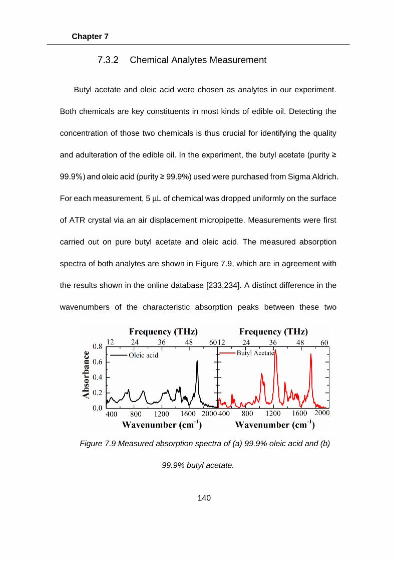
Chapter 7
140
Chemical Analytes Measurement
Butyl acetate and oleic acid were chosen as analytes in our experiment.
Both chemicals are key constituents in most kinds of edible oil. Detecting the
concentration of those two chemicals is thus crucial for identifying the quality
and adulteration of the edible oil. In the experiment, the butyl acetate (purity ≥
99.9%) and oleic acid (purity ≥ 99.9%) used were purchased from Sigma Aldrich.
For each measurement, 5 µL of chemical was dropped uniformly on the surface
of ATR crystal via an air displacement micropipette. Measurements were first
carried out on pure butyl acetate and oleic acid. The measured absorption
spectra of both analytes are shown in Figure 7.9, which are in agreement with
the results shown in the online database [233,234]. A distinct difference in the
wavenumbers of the characteristic absorption peaks between these two
Figure 7.9 Measured absorption spectra of (a) 99.9% oleic acid and (b)
99.9% butyl acetate.
Chapter 7
141
chemicals was observed due to their different molecular structure.
For example in the absorption spectra of oleic acid, the first fingerprint
region between 660 cm-1 and 740 cm-1 are due to the overlapping of out-of-
plane vibration of cis-disubstituted olefins and CH2 rocking vibrations, the
absorption peak at 933 cm-1 is attributed to the O-H out-of-plane bending
vibration, the absorption peak occurring in the region between 1193 cm-1 and
1321 cm-1, 1394 cm-1, 1475 cm-1, and at 1706 cm-1 result from the stretching
vibrations of C-O bond, in-plane O-H bending vibration, and C=O stretching
vibration in the carboxyl functional group [45]. As for butyl acetate, several extra
peaks can be observed at 595 cm-1 to 642 cm-1 which is due to the in-plane
bending vibration of O-C=O group, 1029 cm-1 and 1250 cm-1 which are both led
by the C-O vibration, and 1737 cm-1 due to the C=O stretching vibration from
ester functional group [45]. Furthermore, butyl acetate was then diluted with
different amount of oleic acid and produced four different liquid mixtures, 0.1%,
1%, 10% and 99.9% acetate, for testing the sensitivity of an ATR system in
detecting the concentration of chemicals. The measured absorption spectra for
different concentration of butyl acetate are plotted and compared in Figure 7.10.
The extinction ratio spectra between the chemicals, calculated as ,
where is the measured amplitude of referenced chemical and is
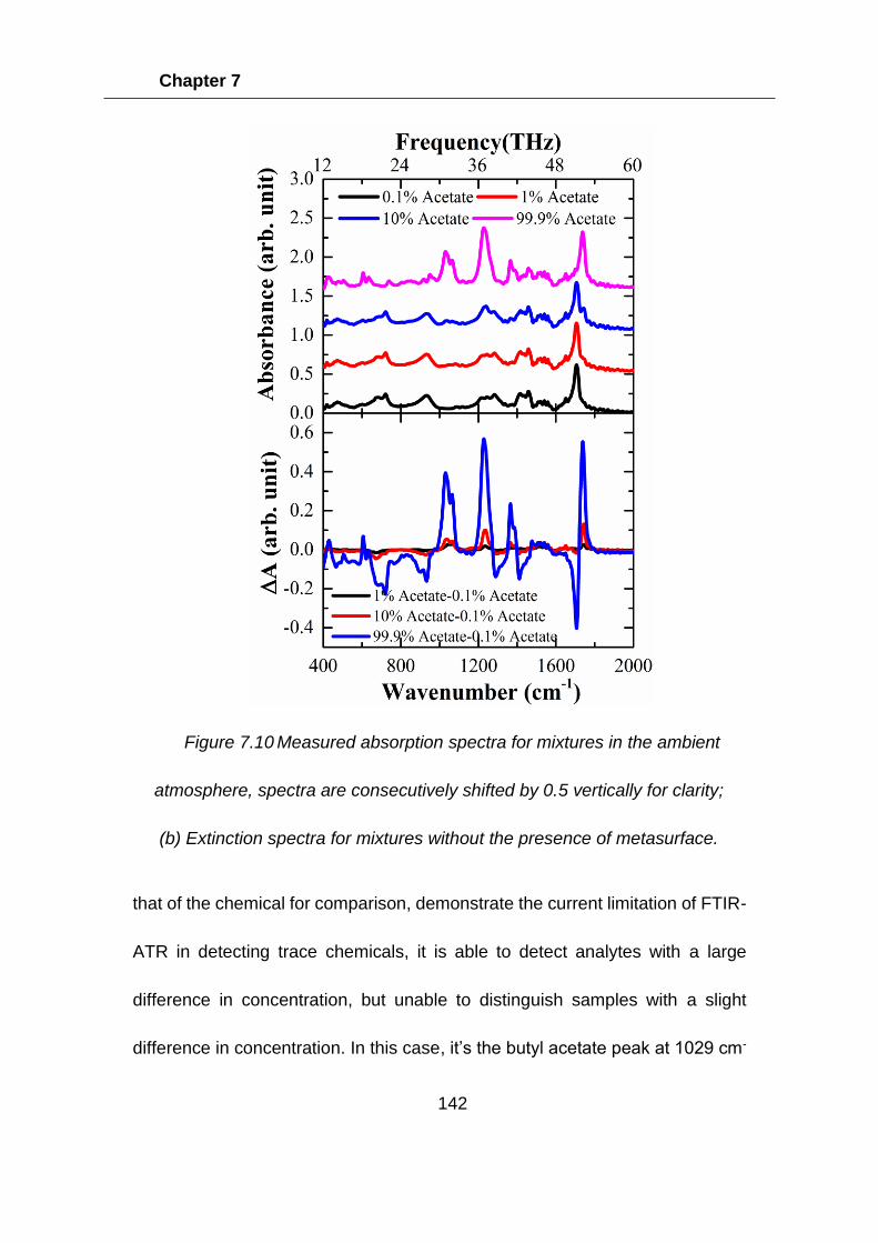
Chapter 7
142
that of the chemical for comparison, demonstrate the current limitation of FTIR-
ATR in detecting trace chemicals, it is able to detect analytes with a large
difference in concentration, but unable to distinguish samples with a slight
difference in concentration. In this case, it’s the butyl acetate peak at 1029 cm-
Figure 7.10 Measured absorption spectra for mixtures in the ambient
atmosphere, spectra are consecutively shifted by 0.5 vertically for clarity;
(b) Extinction spectra for mixtures without the presence of metasurface.
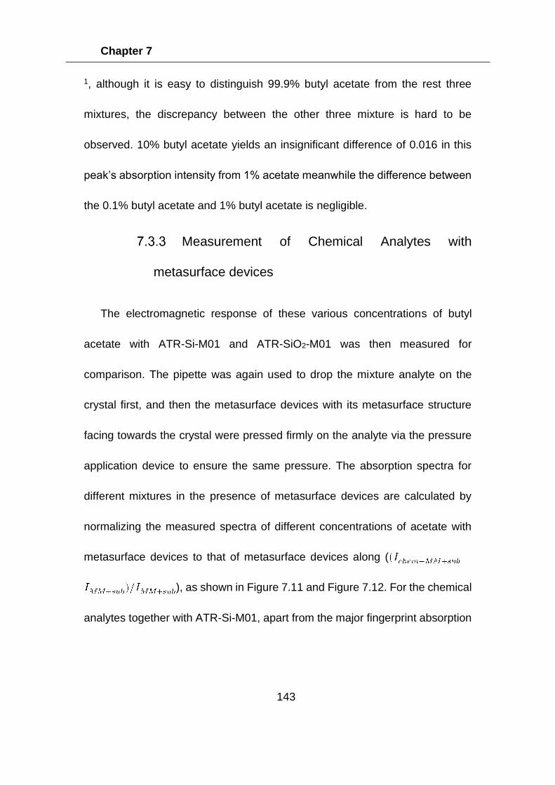
Chapter 7
143
1, although it is easy to distinguish 99.9% butyl acetate from the rest three
mixtures, the discrepancy between the other three mixture is hard to be
observed. 10% butyl acetate yields an insignificant difference of 0.016 in this
peak’s absorption intensity from 1% acetate meanwhile the difference between
the 0.1% butyl acetate and 1% butyl acetate is negligible.
Measurement of Chemical Analytes with
metasurface devices
The electromagnetic response of these various concentrations of butyl
acetate with ATR-Si-M01 and ATR-SiO2-M01 was then measured for
comparison. The pipette was again used to drop the mixture analyte on the
crystal first, and then the metasurface devices with its metasurface structure
facing towards the crystal were pressed firmly on the analyte via the pressure
application device to ensure the same pressure. The absorption spectra for
different mixtures in the presence of metasurface devices are calculated by
normalizing the measured spectra of different concentrations of acetate with
metasurface devices to that of metasurface devices along (
), as shown in Figure 7.11 and Figure 7.12. For the chemical
analytes together with ATR-Si-M01, apart from the major fingerprint absorption
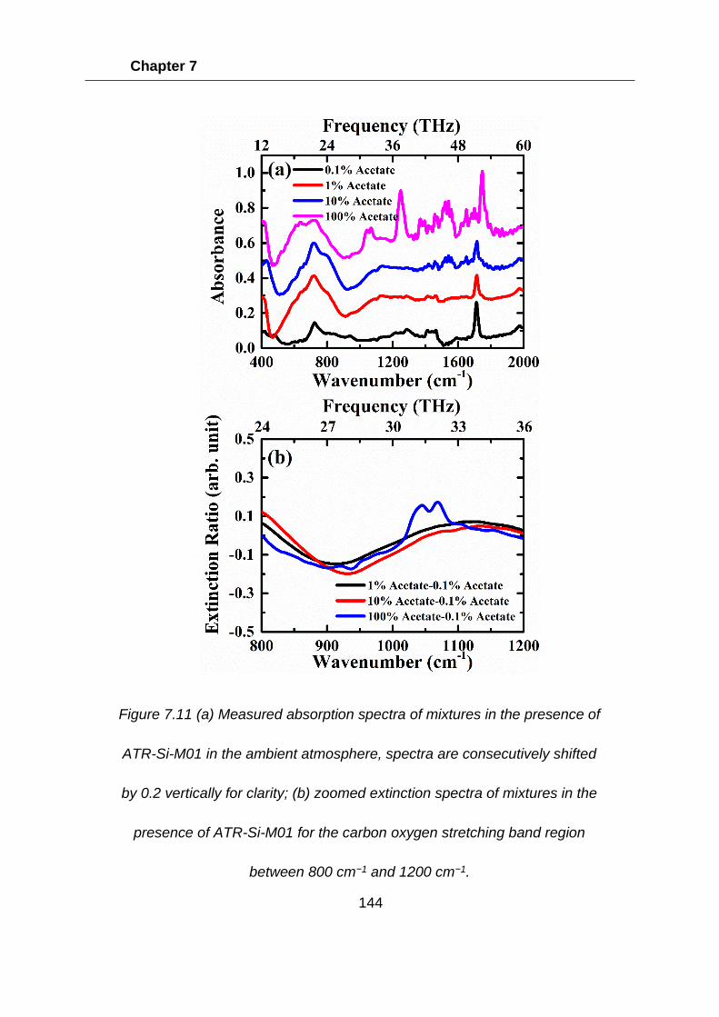
Chapter 7
144
Figure 7.11 (a) Measured absorption spectra of mixtures in the presence of
ATR-Si-M01 in the ambient atmosphere, spectra are consecutively shifted
by 0.2 vertically for clarity; (b) zoomed extinction spectra of mixtures in the
presence of ATR-Si-M01 for the carbon oxygen stretching band region
between 800 cm−1 and 1200 cm−1.
Chapter 7
145
peaks which introduced in the article above, two main dips can be observed at
500 cm-1 and 950 cm-1 in Figure 7.11(a). These two dips resulted from the dipole
and quadrupole resonance modes of the metasurface, proved that the
interaction of metasurface on chemical analytes. These two resonance modes
also shifted to a lower frequency with the increase in the concentration of butyl
acetate. In this case, as the refractive index of butyl acetate is higher than that
of oleic oil, this leads to the effective refractive index of metasurface with
biological samples becomes higher with the increasing percentage of butyl
acetate. However, apart from this tiny blue shift of both resonance dips, it is still
not trivial to tell the difference between 0.1%, 1% and 10% butyl acetate from
the extinction spectrum shown in Figure 7.11(b). For the measurements of
chemical analytes with the presence of ATR-SiO2-M01, there is much more
overlap between the resonance modes of the metasurface and the vibrational
modes in butyl acetate. This overlap has a strong effect on the measured FTIR-
ATR spectra for the different mixtures on the metasurface, which are plotted in
Figure 7.12(a). The plot of the extinction ratio, Figure 7.12(b), shows how the
shape of the spectra now changes with the concentration of butyl acetate,
indicative of coupling between the vibrational resonance of butyl acetate at
1029 cm-1 and the hybridised metamaterial phonon mode. As the concentration
of acetate increases, the minimum seen at ∼1000 cm−1 (marked by a black
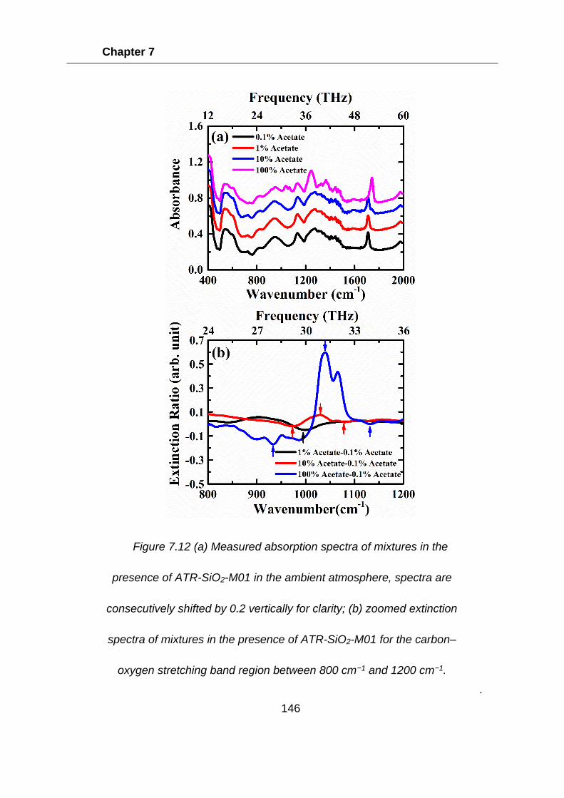
Chapter 7
146
.
Figure 7.12 (a) Measured absorption spectra of mixtures in the
presence of ATR-SiO2-M01 in the ambient atmosphere, spectra are
consecutively shifted by 0.2 vertically for clarity; (b) zoomed extinction
spectra of mixtures in the presence of ATR-SiO2-M01 for the carbon–
oxygen stretching band region between 800 cm−1 and 1200 cm−1.
Chapter 7
147
arrow) splits into two minima (marked by up arrows in red) and form maxima in
the middle (marked by a down arrow in red). In this case, even in the mixture
containing only 1% butyl acetate, a clear maximum is seen in the measured
spectra at around 1020 cm−1. The coupling becomes even stronger for pure
butyl acetate (see blue arrows), which results into the increase in the extinction
ratio.
In summary, a COMSOL model was first used to generate evanescent wave
as that produced by an FTIR spectroscopy with ATR configuration. With the
assistance of this ATR-equivalent model, a complimentary annual ring
resonator was investigated. Numerical simulation results present that at certain
wavenumbers, the metasurface will produce resonance in a dipole mode, and
this resonance mode will split into higher even-order resonance mode with
increasing wavenumber. The electric field distribution also confirms that the
electric field will be trapped in the annual gap at resonance modes which will
potentially increase the sensitivity of ATR spectroscopy due to the
enhancement in the interaction between molecular vibrations and the mid-
infrared evanescent waves in an ATR setup. The design was patterned onto
both Si and Si/SiO2 substrates as simulation shown that the phonon modes in
SiO2 should couple with the metasurface resonance mode according to the
simulation and further increase the sensitivity of the measurement. The spectral
Chapter 7
148
properties of both devices were characterised using an FTIR-ATR system.
Resonant features were observed corresponding to the resonance of the
metasurface on the Si substrate device, and the hybrid resonance of phonon
modes and metasurface resonance on the Si/SiO2 substrate, both in good
agreement with simulations. Preliminary experiments were undertaken using
four different mixtures of butyl acetate diluted with oleic acid. Without the use
of a metasurface, the minimum concentration of butyl acetate that could be
detected was 10%, whereas the use of the metasurface on the Si/SiO2
substrate allowed the detection of 1%, due to the coupling of the vibrational
resonances of the butyl acetate with the hybridised metamaterial phonon mode.
These results demonstrate the potential of the use of metamaterials to improve
the sensitivity of FTIR-ATR measurements, and offers a new route for improved
trace chemical detection.
Chapter 8
149
8 Graphene-based Mid-infrared Modulator
Introduction
It has been illustrated in the last two chapters that a metasurface can be
used to control mid-infrared light spectrally and spatially. However, the
metasurface devices described so far are considered to be passive as their
response to mid-infrared light are fixed with the geometric parameters of the
metasurface structure. For example, to change the emission wavelength of the
metasurface-based graphene thermal emitter introduced in Chapter 6, another
emitter with different geometric parameters has to be fabricated to achieve this
goal. Lack of sufficient tunability limits the applications of conventional
metasurface devices in certain fields like high data rate communication
[132,133], reconfigurable surfaces [235,236], and imaging [237], etc. Intensive
efforts have been made to control the response of metasurface devices
dynamically [132-238], as modulators are of paramount importance for tunable
devices. Although those fast, highly tunable modulator can easily be achieved
by integrating metasurfaces with varactor diodes for millimetre wave [123,235]
or compound of semiconductors like GaAs for terahertz band [132], such
modulators in the mid-infrared range remain challenging due to a limited choice
Chapter 8
150
of materials. Modulators based on electrical controlled liquid crystal (LC) [122]
or thermal controlled vanadium dioxide (VO2) [135] suffer from slow modulation
speed, while others based on semiconductor quantum wells require precise
control on material growth and temperature [238]. Recent work has also
investigated devices based on a combination of a MEMS (micro-electro-
mechanical-system) platform and metasurface to steer mid-infrared light [239],
but such devices require sophisticated integration techniques to realize.
Thanks to its unique gapless band structure, graphene, whose carrier
density can be easily and smoothly controlled by shifting the Fermi levels,
provides a highly tunable conductivity via electrostatic gating, or optical
excitation [210,240,241]. This modulation usually can be accomplished within
the order of nanoseconds, far quicker than the conventional LC and VO2
modulators. Thus, integrating graphene into metasurface is a promising
approach for designing active mid-infrared modulators. Although up to now,
theoretical studies have been intensively conducted on patterned graphene
modulator [242,243] and graphene-integrated metasurface modulator [244-
247], not too many experimental results are reported.
In this chapter, we present the experimental demonstration of a high-speed,
compact graphene integrated metasurface mid-infrared modulator, which
Chapter 8
151
allows a wide range of amplitude and phase modulations by tuning the Fermi
level of graphene with gate voltage control. The tunability achieved by the
design architecture of our device is essential for obtaining a highly modulated
phase under ambient conditions. Furthermore, a prototype mid-infrared
reconfigurable surface is proposed to function as a beam steering lens,
realizing the switch from normal reflection to anomalous reflection with a high
conversion efficiency and responding time.
Design
Our design integrates monolayer chemical vapour deposition (CVD)
graphene into a metasurface Salisbury screen absorber, as sketched in Figure
8.1(a). The Salisbury screen absorber, named after American engineer Winfield
Salisbury, was originally designed as an absorbent device for radar detection,
and consists of three layers: a frequency selective surface (FSS) on the top, a
lossless dielectric spacer layer, and a metallic ground plane to block all the
wave propagations. As fully explained in § 2.3.2, the reflection from the device
can be totally eliminated when the impedance matching condition is fulfilled, i.e.
the effective impedance of the device is equal to that of the wave in free
space . The circuit diagram of the structure is shown in Figure 8.1(b), in
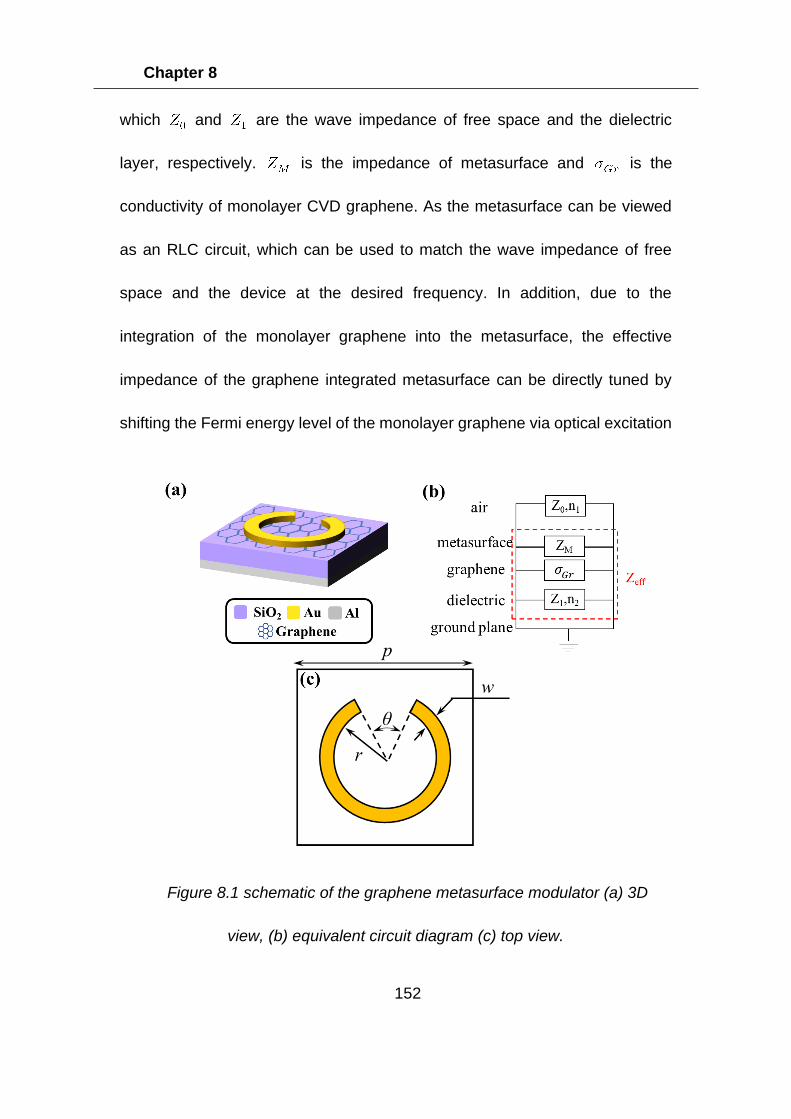
Chapter 8
152
which and are the wave impedance of free space and the dielectric
layer, respectively. is the impedance of metasurface and is the
conductivity of monolayer CVD graphene. As the metasurface can be viewed
as an RLC circuit, which can be used to match the wave impedance of free
space and the device at the desired frequency. In addition, due to the
integration of the monolayer graphene into the metasurface, the effective
impedance of the graphene integrated metasurface can be directly tuned by
shifting the Fermi energy level of the monolayer graphene via optical excitation
Figure 8.1 schematic of the graphene metasurface modulator (a) 3D
view, (b) equivalent circuit diagram (c) top view.
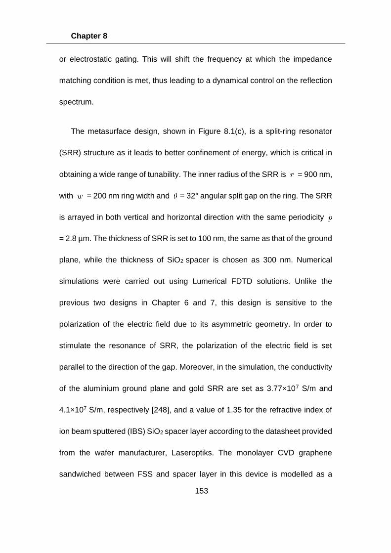
Chapter 8
153
or electrostatic gating. This will shift the frequency at which the impedance
matching condition is met, thus leading to a dynamical control on the reflection
spectrum.
The metasurface design, shown in Figure 8.1(c), is a split-ring resonator
(SRR) structure as it leads to better confinement of energy, which is critical in
obtaining a wide range of tunability. The inner radius of the SRR is = 900 nm,
with = 200 nm ring width and = 32° angular split gap on the ring. The SRR
is arrayed in both vertical and horizontal direction with the same periodicity
= 2.8 µm. The thickness of SRR is set to 100 nm, the same as that of the ground
plane, while the thickness of SiO2 spacer is chosen as 300 nm. Numerical
simulations were carried out using Lumerical FDTD solutions. Unlike the
previous two designs in Chapter 6 and 7, this design is sensitive to the
polarization of the electric field due to its asymmetric geometry. In order to
stimulate the resonance of SRR, the polarization of the electric field is set
parallel to the direction of the gap. Moreover, in the simulation, the conductivity
of the aluminium ground plane and gold SRR are set as 3.77×10⁷ S/m and
4.1×10⁷ S/m, respectively [248], and a value of 1.35 for the refractive index of
ion beam sputtered (IBS) SiO2 spacer layer according to the datasheet provided
from the wafer manufacturer, Laseroptiks. The monolayer CVD graphene
sandwiched between FSS and spacer layer in this device is modelled as a
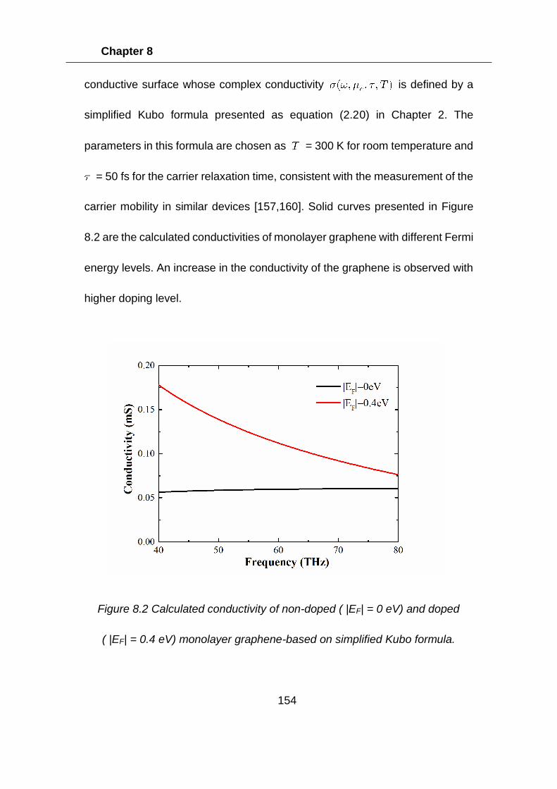
Chapter 8
154
conductive surface whose complex conductivity is defined by a
simplified Kubo formula presented as equation (2.20) in Chapter 2. The
parameters in this formula are chosen as = 300 K for room temperature and
= 50 fs for the carrier relaxation time, consistent with the measurement of the
carrier mobility in similar devices [157,160]. Solid curves presented in Figure
8.2 are the calculated conductivities of monolayer graphene with different Fermi
energy levels. An increase in the conductivity of the graphene is observed with
higher doping level.
Figure 8.2 Calculated conductivity of non-doped ( |EF| = 0 eV) and doped
( |EF| = 0.4 eV) monolayer graphene-based on simplified Kubo formula.
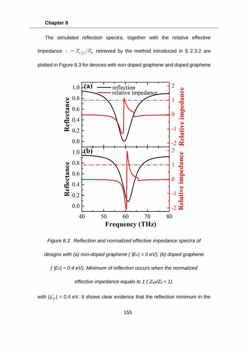
Chapter 8
155
The simulated reflection spectra, together with the relative effective
impedance retrieved by the method introduced in § 2.3.2 are
plotted in Figure 8.3 for devices with non-doped graphene and doped graphene
with | | = 0.4 eV. It shows clear evidence that the reflection minimum in the
Figure 8.3 Reflection and normalized effective impedance spectra of
designs with (a) non-doped graphene ( |EF| = 0 eV); (b) doped graphene
( |EF| = 0.4 eV). Minimum of reflection occurs when the normalized
effective impedance equals to 1 ( Zeff/Z0 = 1).
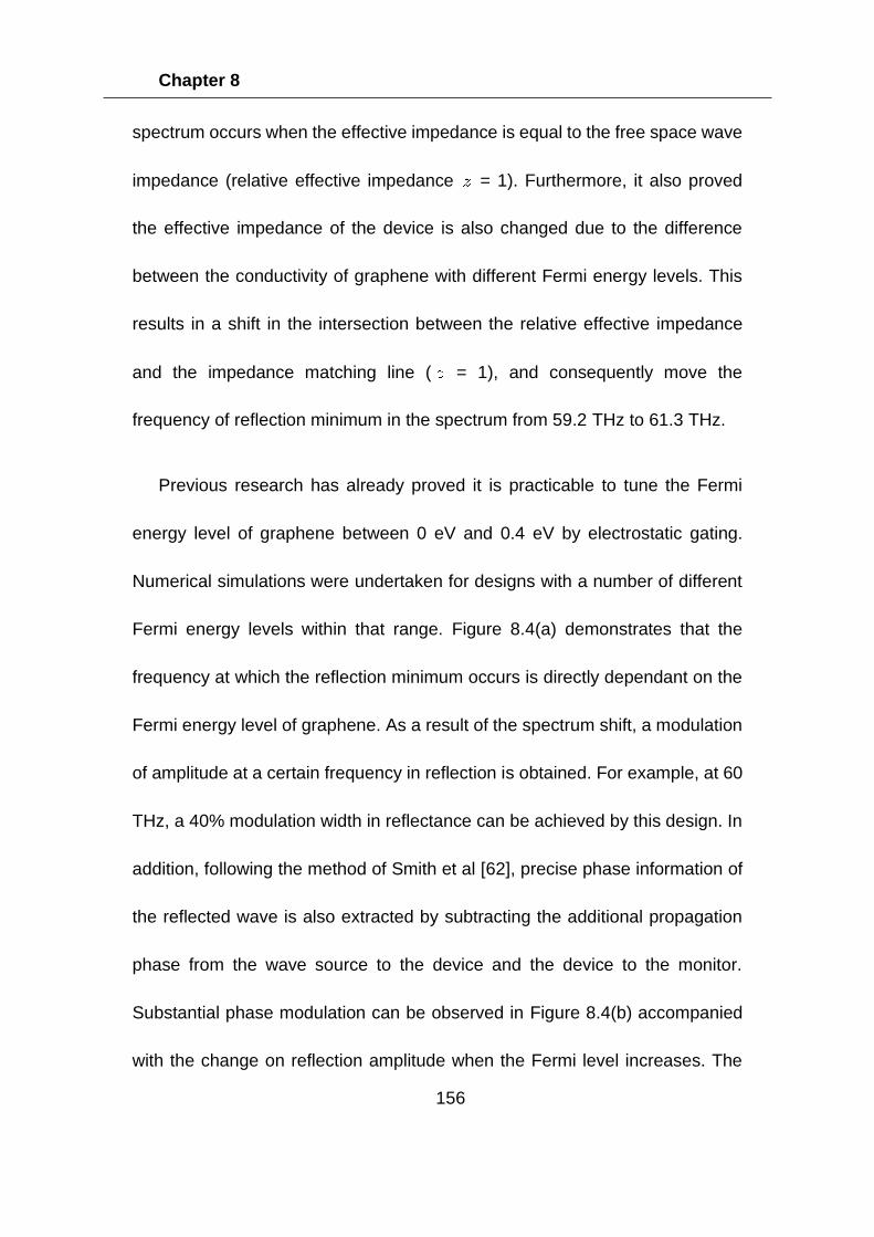
Chapter 8
156
spectrum occurs when the effective impedance is equal to the free space wave
impedance (relative effective impedance = 1). Furthermore, it also proved
the effective impedance of the device is also changed due to the difference
between the conductivity of graphene with different Fermi energy levels. This
results in a shift in the intersection between the relative effective impedance
and the impedance matching line ( = 1), and consequently move the
frequency of reflection minimum in the spectrum from 59.2 THz to 61.3 THz.
Previous research has already proved it is practicable to tune the Fermi
energy level of graphene between 0 eV and 0.4 eV by electrostatic gating.
Numerical simulations were undertaken for designs with a number of different
Fermi energy levels within that range. Figure 8.4(a) demonstrates that the
frequency at which the reflection minimum occurs is directly dependant on the
Fermi energy level of graphene. As a result of the spectrum shift, a modulation
of amplitude at a certain frequency in reflection is obtained. For example, at 60
THz, a 40% modulation width in reflectance can be achieved by this design. In
addition, following the method of Smith et al [62], precise phase information of
the reflected wave is also extracted by subtracting the additional propagation
phase from the wave source to the device and the device to the monitor.
Substantial phase modulation can be observed in Figure 8.4(b) accompanied
with the change on reflection amplitude when the Fermi level increases. The
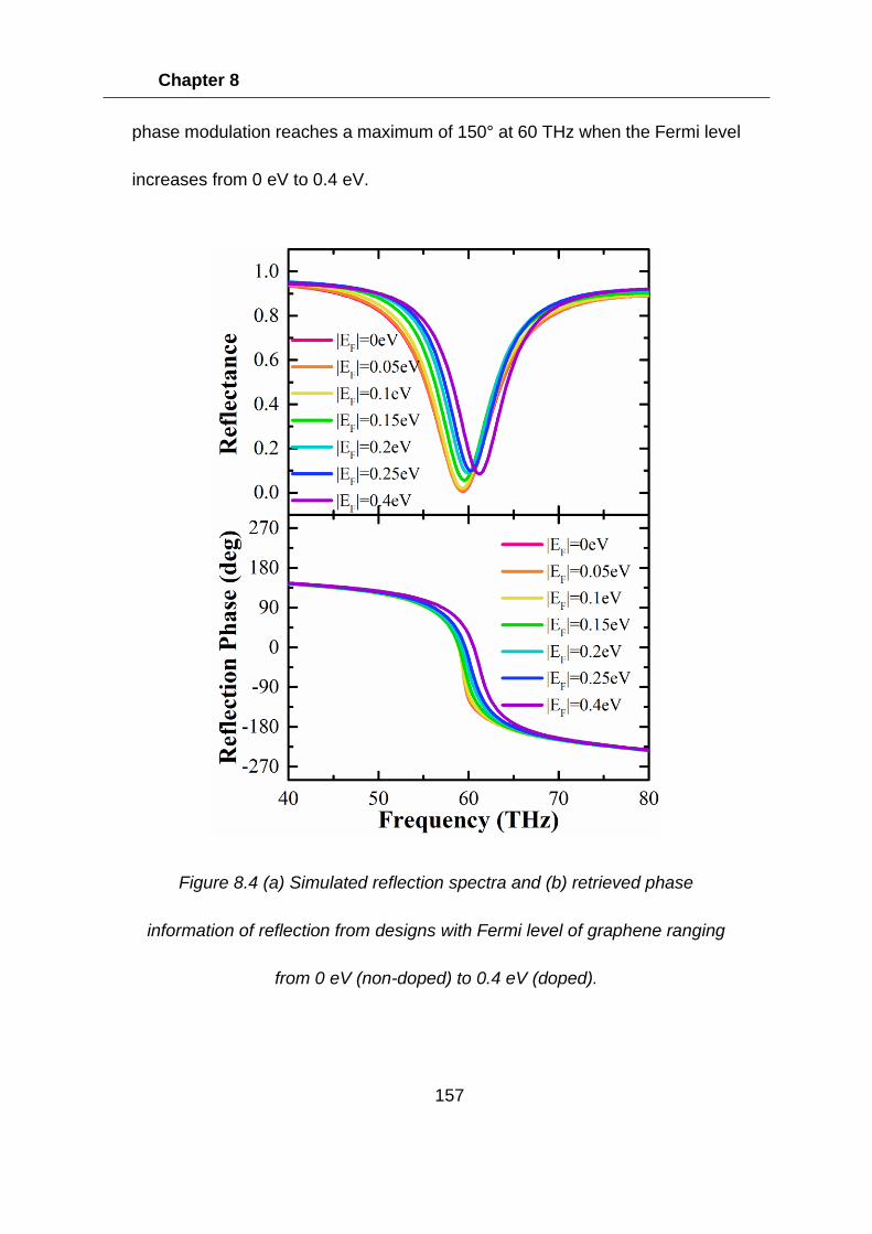
Chapter 8
157
phase modulation reaches a maximum of 150° at 60 THz when the Fermi level
increases from 0 eV to 0.4 eV.
Figure 8.4 (a) Simulated reflection spectra and (b) retrieved phase
information of reflection from designs with Fermi level of graphene ranging
from 0 eV (non-doped) to 0.4 eV (doped).
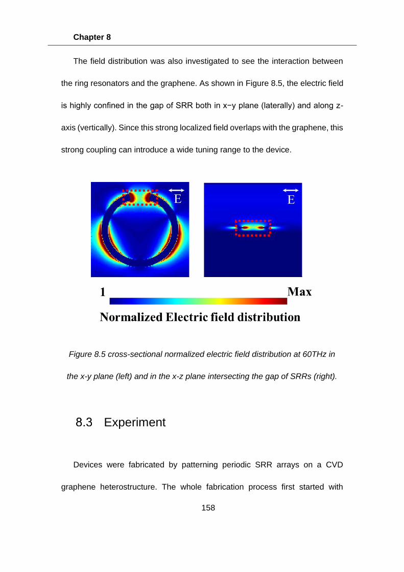
Chapter 8
158
The field distribution was also investigated to see the interaction between
the ring resonators and the graphene. As shown in Figure 8.5, the electric field
is highly confined in the gap of SRR both in x−y plane (laterally) and along z-
axis (vertically). Since this strong localized field overlaps with the graphene, this
strong coupling can introduce a wide tuning range to the device.
Experiment
Devices were fabricated by patterning periodic SRR arrays on a CVD
graphene heterostructure. The whole fabrication process first started with
Figure 8.5 cross-sectional normalized electric field distribution at 60THz in
the x-y plane (left) and in the x-z plane intersecting the gap of SRRs (right).
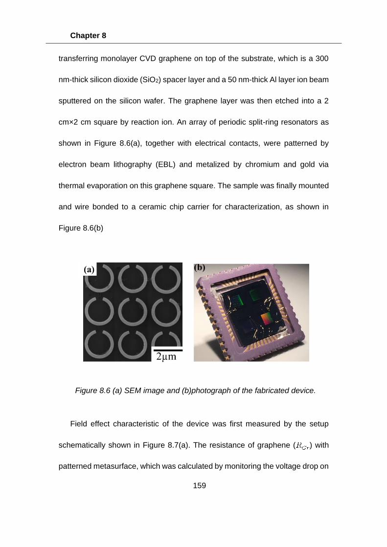
Chapter 8
159
transferring monolayer CVD graphene on top of the substrate, which is a 300
nm-thick silicon dioxide (SiO2) spacer layer and a 50 nm-thick Al layer ion beam
sputtered on the silicon wafer. The graphene layer was then etched into a 2
cm×2 cm square by reaction ion. An array of periodic split-ring resonators as
shown in Figure 8.6(a), together with electrical contacts, were patterned by
electron beam lithography (EBL) and metalized by chromium and gold via
thermal evaporation on this graphene square. The sample was finally mounted
and wire bonded to a ceramic chip carrier for characterization, as shown in
Figure 8.6(b)
Field effect characteristic of the device was first measured by the setup
schematically shown in Figure 8.7(a). The resistance of graphene ( ) with
patterned metasurface, which was calculated by monitoring the voltage drop on
Figure 8.6 (a) SEM image and (b)photograph of the fabricated device.
Chapter 8
160
the electrodes ( ) with a constant 100 nA source-drain current ( ), is
measured as a function of the applied gate voltage ( ).The calculated
resistance is then compared to that of the device without the metasurface.
Measured field effect curves plotted in Figure 8.7(b), without too many
differences, both show a peak value of resistance at ≈ 60 V corresponding
to the charge neutral point (CNP) where Fermi level is at Dirac point (| | = 0
eV). Such result suggests that the metasurface doesn’t have a huge impact on
the field effect characteristic of the graphene as expected, and the CVD
graphene used has a significant intrinsic hole doping indicated by the large
positive value of which is consistent with the previous experimental
results [160].
Investigations were then conducted on how the reflection spectrum of the
device can be dynamically controlled by the gate voltage driven on the device,
the sample was mounted on a chip holder and measured in an FTIR
spectroscopy with reflection setup. A polarizer was added to ensure the mid-
infrared light sourced from FTIR is linearly polarized in the direction parallel to
the gap of the SRRs. A surface scan was then run to locate the position of the
metasurface structures and the spatial variation of reflectance is shown in
Figure 8.8(a). The area with the smallest overall measured reflection intensity,
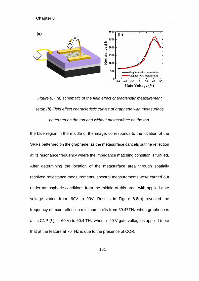
Chapter 8
161
the blue region in the middle of the image, corresponds to the location of the
SRRs patterned on the graphene, as the metasurface cancels out the reflection
at its resonance frequency where the impedance matching condition is fulfilled.
After determining the location of the metasurface area through spatially
resolved reflectance measurements, spectral measurements were carried out
under atmospheric conditions from the middle of this area, with applied gate
voltage varied from -90V to 90V. Results in Figure 8.8(b) revealed the
frequency of main reflection minimum shifts from 59.47THz when graphene is
at its CNP ( = 60 V) to 60.4 THz when a -90 V gate voltage is applied (note
that at the feature at 70THz is due to the presence of CO2).
Figure 8.7 (a) schematic of the field effect characteristic measurement
setup (b) Field effect characteristic curves of graphene with metasurface
patterned on the top and without metasurface on the top.
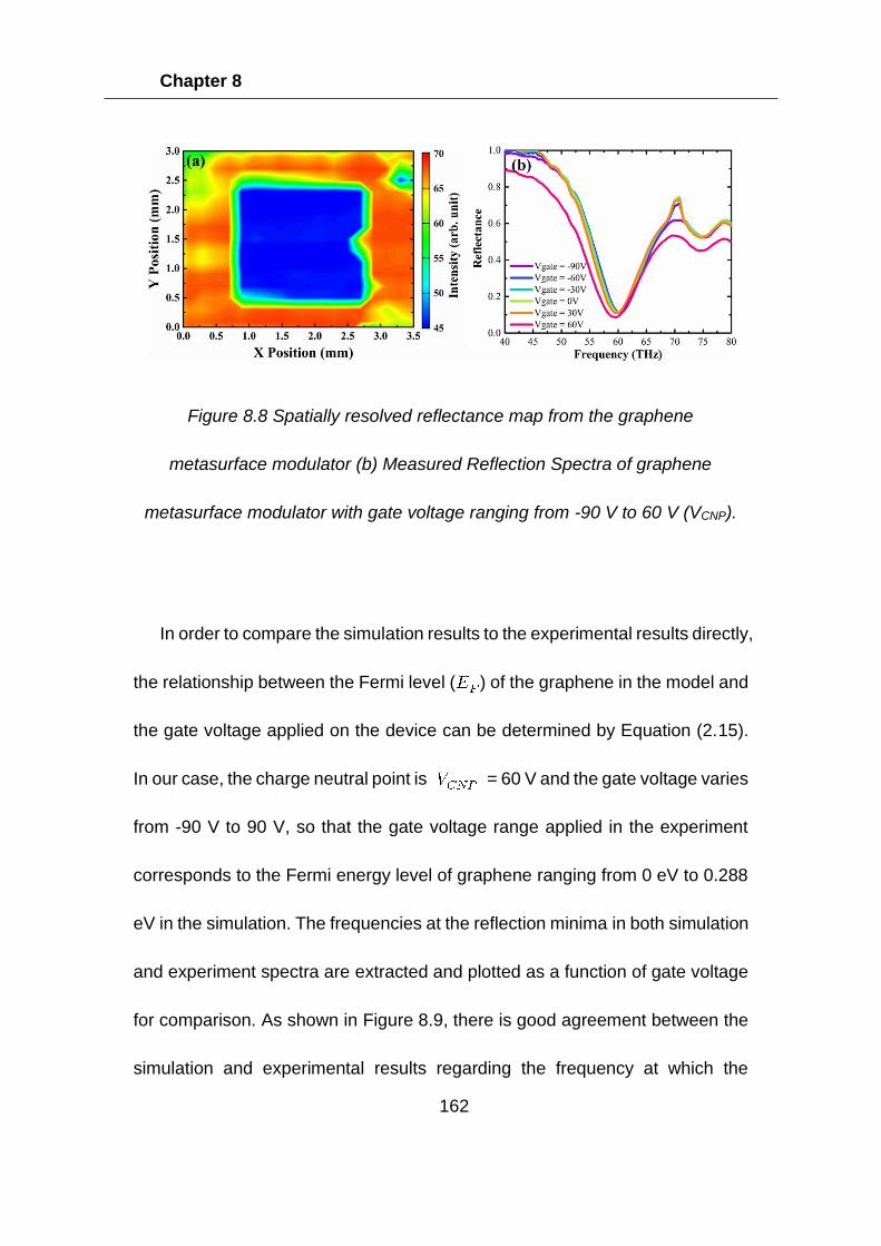
Chapter 8
162
In order to compare the simulation results to the experimental results directly,
the relationship between the Fermi level ( ) of the graphene in the model and
the gate voltage applied on the device can be determined by Equation (2.15).
In our case, the charge neutral point is = 60 V and the gate voltage varies
from -90 V to 90 V, so that the gate voltage range applied in the experiment
corresponds to the Fermi energy level of graphene ranging from 0 eV to 0.288
eV in the simulation. The frequencies at the reflection minima in both simulation
and experiment spectra are extracted and plotted as a function of gate voltage
for comparison. As shown in Figure 8.9, there is good agreement between the
simulation and experimental results regarding the frequency at which the
Figure 8.8 Spatially resolved reflectance map from the graphene
metasurface modulator (b) Measured Reflection Spectra of graphene
metasurface modulator with gate voltage ranging from -90 V to 60 V (VCNP).
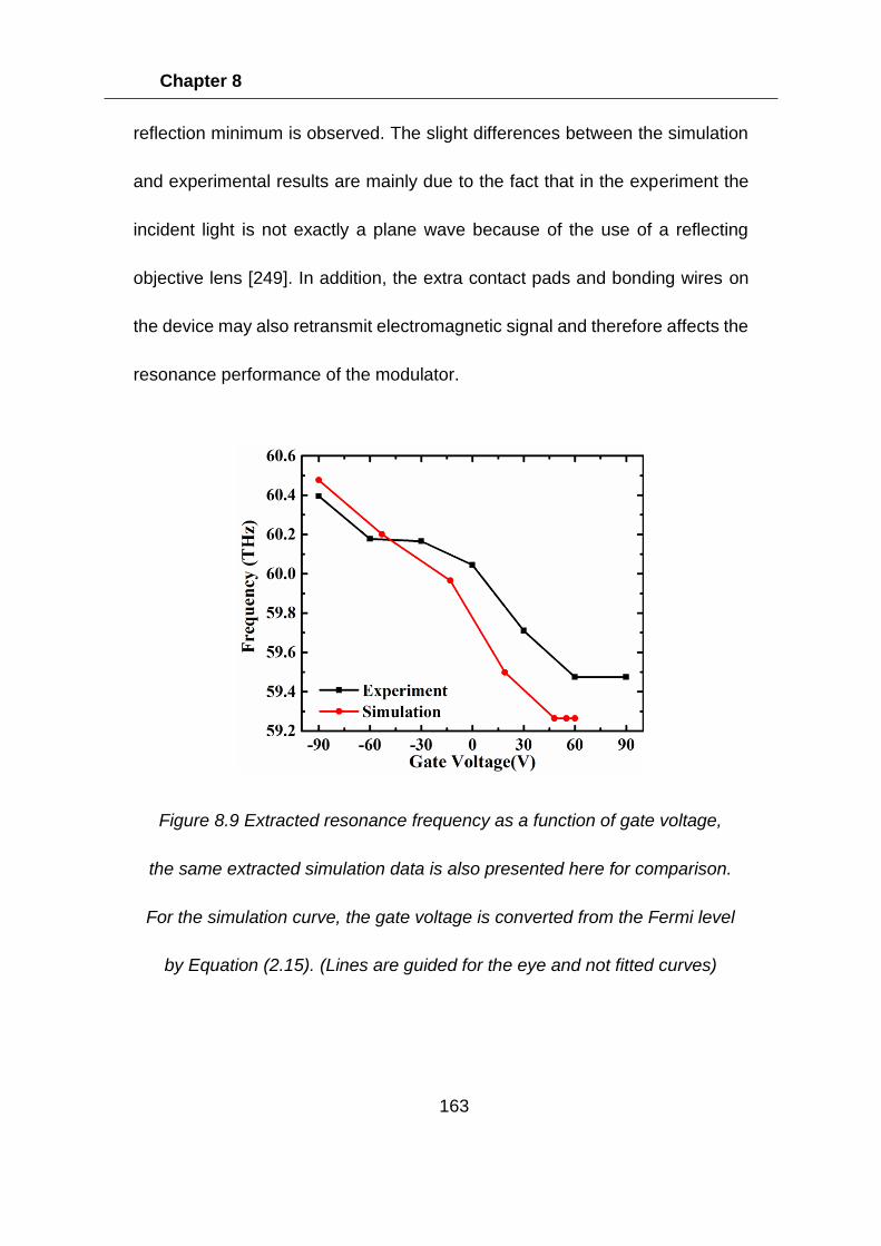
Chapter 8
163
reflection minimum is observed. The slight differences between the simulation
and experimental results are mainly due to the fact that in the experiment the
incident light is not exactly a plane wave because of the use of a reflecting
objective lens [249]. In addition, the extra contact pads and bonding wires on
the device may also retransmit electromagnetic signal and therefore affects the
resonance performance of the modulator.
Figure 8.9 Extracted resonance frequency as a function of gate voltage,
the same extracted simulation data is also presented here for comparison.
For the simulation curve, the gate voltage is converted from the Fermi level
by Equation (2.15). (Lines are guided for the eye and not fitted curves)
Chapter 8
164
Application
The wide amplitude and phase modulation achieved by our modulator
design make it an ideal building block for reconfigurable metasurfaces, which
have a wide range of promising applications such as countermeasures to radar
detection [235], compact lenses [250,251], beam steering devices [130,252],
dynamic holograms [236,253,254], just name a few. Here we construct a
reconfigurable metasurface by using the same metasurface design with
different geometric parameters. Proof-of-principle simulation results of such
graphene-integrated beam steering metasurface show the capability of
reflecting the reflective beam to an anomalous angle under a normal incident
plane wave at 60 THz when the graphene is electrostatically gated.
As mentioned in § 2.3.2 if a phase discontinuity is introduced at the interface
between two media, the beam will be reflected to an anomalous angle, which
can be calculated from Equation (2.13). Due to the graphene metasurface
modulator is capable of achieving a wide range of phase modulation, we can
dynamically control the phase gradient along the interface and thus
manipulate the direction of the reflection. The geometric parameters of the
modulator design were swept to find four designs that can cover a linear spatial
phase profile from 0 to 2π at 60 THz when the Fermi level of graphene is 0.4eV
Chapter 8
165
and have nearly identical reflection phases when the Fermi level of graphene
returns to the Dirac point. This enables the interface to reflect the incident wave
specularly when no gate voltage is applied on the lens, and to deflect the wave
anomaly when a gate voltage is driven.
The geometric parameters of four specifically designed modulators are
shown in Table 8.1. If a lens is constructed by periodically aligning four
modulators into a 4×1 super cell as illustrated in Figure 8.10(a), the phase
profile in Figure 8.10(b) shows that there is a neglectable phase discontinuity
in the phase profile along the interface when the graphene is non-doped (
= 0 eV) ,and when the graphene is doped, a = π/2 phase increment
between two adjacent modulators along x-axis direction will be established as
soon as the Fermi level of graphene increase to 0.4eV. In this case, by changing
the voltage added on the metasurface lens directly, we can alter the reflection
angle from 0° to 29.6° at 60THz, according to equation (2.13). Figure 8.11(a)
and (b) demonstrate the simulated farfield scattering pattern of the device in
polar coordinates, which clearly show the beam is steered by 30°, in great
agreement with the theoretical reflection angle. The steering efficiency, the
intensity of wave at deflection angle normalized to that of the incident wave,
can reach up to 45%, can be attained. This efficiency can be even higher if
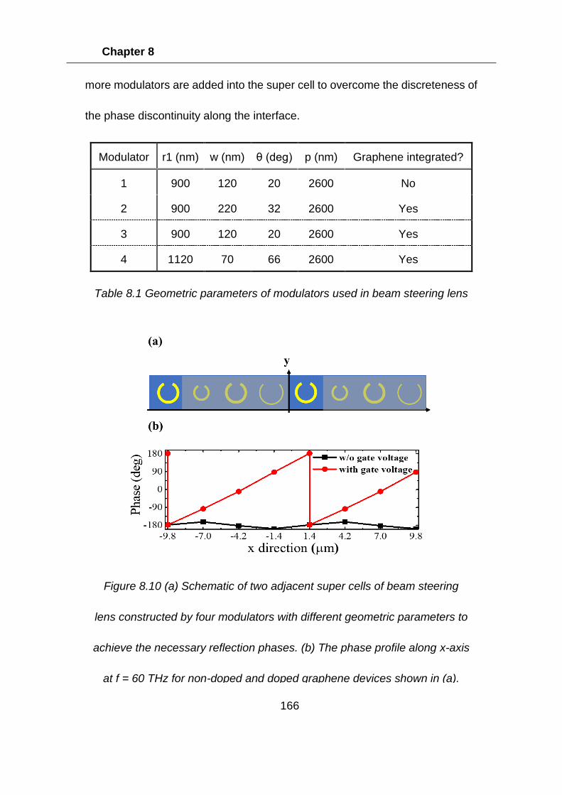
Chapter 8
166
more modulators are added into the super cell to overcome the discreteness of
the phase discontinuity along the interface.
Modulator r1 (nm) w (nm) θ (deg) p (nm) Graphene integrated?
1 900 120 20 2600 No
2 900 220 32 2600 Yes
3 900 120 20 2600 Yes
4 1120 70 66 2600 Yes
Table 8.1 Geometric parameters of modulators used in beam steering lens
Figure 8.10 (a) Schematic of two adjacent super cells of beam steering
lens constructed by four modulators with different geometric parameters to
achieve the necessary reflection phases. (b) The phase profile along x-axis
at f = 60 THz for non-doped and doped graphene devices shown in (a).
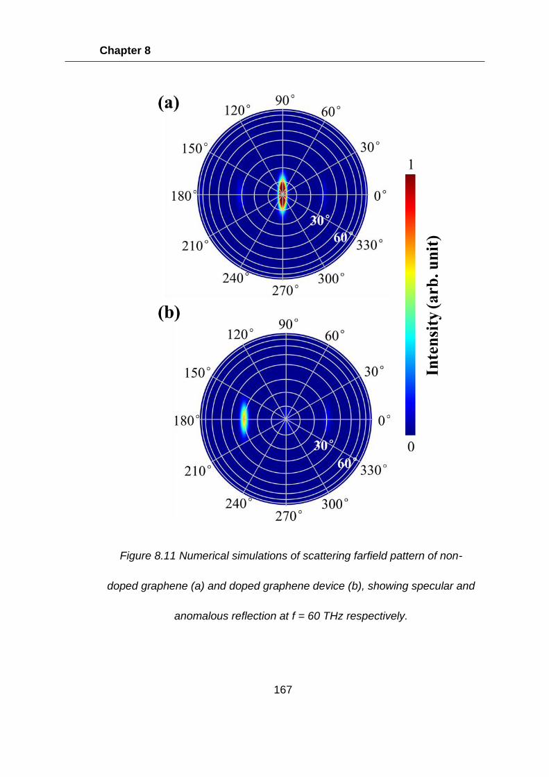
Chapter 8
167
Figure 8.11 Numerical simulations of scattering farfield pattern of non-
doped graphene (a) and doped graphene device (b), showing specular and
anomalous reflection at f = 60 THz respectively.
Chapter 8
168
Summary
In this chapter, it is shown that the electromagnetic response of the
metasurface design can be manipulated via applying voltage on it by integrating
monolayer graphene into it. The variation in the conductivity of graphene
caused by tuning the gate voltage applied to it will change the effective
impedance of the graphene integrated metasurface design and thus shift its
reflection spectrum. The design proposed in this chapter, a graphene-
integrated SRR Salisbury screen, is able to achieve a good tunability by
enhancing the nonlinear response of graphene via localizing the electric field
on it. Numerical simulations show that due to the strong confinement at the split
gap of SRR, the design is able to achieve a 50% modulation width in reflectance
and 150° in reflection phase when the Fermi level of graphene is altered from
0eV to 0.4eV accordingly. The fabricated modulator was then tested in an FTIR
reflection setup, although only a 0.288eV Fermi level can be achieved, it is still
observed that the resonant frequency at which the minimum in reflection occurs
can be directly controlled by an applied bias, with the size of the shift being in
good agreement with the simulations. We also demonstrate the feasibility of
creating a beam steering lens by constructing four such modulators but with
different geometric parameters as a new super cell. Simulations show that, as

Chapter 8
169
a 0 to 2π phase variation over the super cell will be established as soon as the
Fermi level of graphene is increased to 0.4 eV, the metasurface lens will reflect
the beam with an extra 30° compared to when the graphene is undoped.
Chapter 9
170
9 Conclusions and Outlook
The work presented in this thesis focuses on the development of a
series of new generation mid-infrared devices which are compact in size
and powerful in performance. Three different devices, narrowband mid-
infrared thermal emitter, wave trapping sensor, and phase modulators
were designed exploiting the unique properties of the two ultrathin
building blocks: metasurface and graphene. Preliminary prototypes were
fabricated in a cleanroom using modern semiconductor fabrication
technology like RIE etching, e-beam lithography, and thermal
evaporation. Results measured under different setups based on FTIR
spectroscopy showed good agreement with simulation results.
However, it should be noted that there is still room to improve the
performance of the devices described in Chapter 6,7,8. Some of the latest
work on metasurface design and graphene synthesis, which could benefit
our devices are highlighted in Section 9.2.
Chapter 9
171
Conclusions
Metasurface-based Narrowband Graphene
Thermal Emitter
A metasurface, composed of two groups of metallic annular rings
in diagonal and off-diagonal directions, was designed as a frequency
selective surface and integrated into the graphene thermal emitter for
reducing the emission bandwidth. Simulation, as well as experiment
results, show that the broadband emission from the Joule heating of the
graphene filament is tailored into two narrow windows, which directly
related to the resonance frequencies of both groups of annular ring
resonators. The resonance of annual rings will constructively interferes
with the thermal radiation from the graphene filament, leading to maxima
in the emission spectra at wavelengths determined by their geometry.
Simulations also show that the addition of a conducting layer below the
emitting layer greatly increases the Q-factor of the maximum in the
emission spectrum.
The possibility of tailoring the emission characteristics of these
devices, which can reduce manufacturing costs and allow for modulation
Chapter 9
172
at relatively high frequencies, demonstrates their potential for use in
applications such as infrared gas sensing.
Metasurface-enhanced ATR Spectroscopy
In this work, a metasurface was designed to localize and enhance
the field distribution in a small area for increasing the sensitivity of
detecting chemical or other biological samples in an aqueous
environment. Resonant features were observed corresponding to the
resonance of the metasurface on the silicon substrate device, and the
hybrid resonance of phonon modes and metasurface resonance on the
SiO2/Si substrate. Field distribution profiles obtained from the simulation
results suggests the strong localized field enhancement in the nano gap
at the centre of the complimentary ring resonators, where the light-matter
interactions are strengthened. Preliminary experiments were undertaken
in an FTIR-ATR system using mixtures of butyl acetate diluted with oleic
acid. Without the use of a metasurface, the minimum concentration of
butyl acetate that could be detected was 10%, whereas the use of the
metasurface on the SiO2/Si substrate allowed the detection of 1%, due to
the coupling of the vibrational resonances of the butyl acetate with the
hybridised metamaterial phonon mode.
Chapter 9
173
These results demonstrate the potential of the use of
metamaterials to improve the sensitivity of FTIR-ATR measurements,
and offers a new route for improved trace chemical detection.
Graphene based metasurface phase modulator
Graphene is used in conjunction with metasurface to achieve a
dynamic control on the response of the mid-infrared wave. A mid-infrared
reflective modulator was achieved by split-ring resonator and CVD
graphene. When a gate voltage is applied, the Fermi level of graphene is
shifted leading to a change of its conductivity, which will consequently
change the effective impedance at the interface. Simulations show that
the device can achieve a phase modulation up to 150° when the Fermi
level increases from 0eV to 0.4eV. Based on the design of modulator, we
also demonstrate the feasibility of creating a beam steering lens by
constructing four such modulators but with different geometric
parameters as a new super lattice. Simulations show that, as 0 to 2π
phase variation over the unit cell will be established as soon as a gate
voltage is applied, the gated lens will reflect the beam with an extra 30°
compared to when the lens is unbiased.
Chapter 9
174
The compact and ultrafast modulators we proposed could promote
a wide range of mid-infrared application in free-space communications,
imaging, LIDAR, and homeland security, etc
Outlook
Metasurface
Due to the limited choices of fabrication equipment, the
metasurface proposed in this work is all made of gold, which suffers from
drawbacks such as low Q-factor as a result of high Ohmic losses.
However, it has been proved in previous research that strong and high
Q-factor resonance is achievable by using metasurface made of
dielectrics with high permittivity, which can generate magnetic dipoles,
electric dipoles and higher order dipoles due to Mie resonances [255].
This could potentially improve the performance of our metasurface-based
graphene thermal emitter.
Graphene
The area of graphene has become a cutting-edge and promising
researching direction in recent years, but there is still a very long way to
Chapter 9
175
go for the mass production of graphene devices. Although CVD graphene
can now be probed in a very large area, surface impurities introduced
during the synthesis process will introduce detrimental impacts upon the
intrinsic properties of graphene and thus device performances. The
exfoliation method, on the other hand, can provide better quality
graphene with higher purity and superior electrical and thermal
performance, but is not ideal for large-scale monolayer graphene
synthesis. Progress has been made on the research on the synthesis
method of large-area, high quality monolayer graphene sheet. Zhang et
al from Berkley, have recently reported their experiments of dewetting the
catalytic metal during the CVD process [256]. In this case, the graphene
will be directly attached to the dielectric layer which may eliminate
impurities produced from CVD and transfer.
Bibliography
176
Bibliography
1 Krier, A. Mid-infrared semiconductor optoelectronics. Springer (2007).
2 Smith, B. C. Fundamentals of Fourier transform infrared spectroscopy.
CRC Press (2011).
3 Elder, T., & Strong, J. The infrared transmission of atmospheric windows.
Journal of The Franklin Institute 255, 189-208 (1953).
4 Karoui, R., Downey, G. & Blecker, C. Mid-infrared spectroscopy coupled
with chemometrics: A tool for the analysis of intact food systems and the
exploration of their molecular structure-quality relationships-A review.
Chemical Reviews 110, 6144–6168 (2010).
5 Schliesser, A., Picqué, N. & Hänsch, T. W. Mid-infrared frequency combs.
Nature Photonics 6, 440–449 (2012).
6 Aroca, R. F., Ross, D. J. & Domingo, C. Surface-enhanced infrared
spectroscopy. Applied Spectroscopy 58, (2004).
7 Stuart, B. H. Infrared Spectroscopy: Fundamentals and Applications. John
Wiley & Sons (2004).
8 Özcan, L. Ç., Tréanton, V., Kashyap, R. & Martinu, L. High-quality flat-top
micromachining of silica by a CW CO2 laser. IEEE Photonics Technology
Letters 19, 459–461 (2007).
9 Lin, P. T. et al. Mid-infrared spectrometer using opto-nanofluidic slot-
waveguide for label-free on-chip chemical sensing. Nano Letters 14, 231–
238 (2014).
10 Wysocki, G. & Weidmann, D. Molecular dispersion spectroscopy for
chemical sensing using chirped mid-infrared quantum cascade laser.
Optics Express 18, 26123–26140 (2010).
Bibliography
177
11 Soref, R. Mid-infrared photonics in silicon and germanium. Nat. Photonics,
4, 495 (2010).
12 Law, S., Podolskiy, V., & Wasserman, D. Towards nano-scale photonics
with micro-scale photons: the opportunities and challenges of mid-infrared
plasmonics. Nanophotonics 2, 103-130 (2013).
13 Santos, P. M., Pereira-Filho, E. R., & Rodriguez-Saona, L. E. Application
of hand-held and portable infrared spectrometers in bovine milk analysis.
Journal of Agricultural and Food Chemistry 61, 1205-1211 (2013).
14 Lin, C. A., Ayvaz, H., & Rodriguez-Saona, L. E. Application of portable
and handheld infrared spectrometers for determination of sucrose levels
in infant cereals. Food Analytical Methods 7, 1407-1414 (2014).
15 Birkel, E., & Rodriguez‐Saona, L. Application of a portable handheld
infrared spectrometer for quantitation of trans fat in edible oils. Journal of
the American Oil Chemists' Society 88, 1477-1483 (2011).
16 Wright, A. F., & Dupuy, J. Glass... current issues. Springer Science &
Business Media (2012).
17 Soref, R. Mid-infrared photonics in silicon and germanium. Nature
Photonics, 4, 495 (2010).
18 Harris, D. C. Materials for infrared windows and domes: properties and
performance. SPIE Press (1999).
19 Mahlmeister, N. H., Lawton, L. M., Luxmoore, I. J., & Nash, G. R.
Modulation characteristics of graphene-based thermal emitters. Applied
Physics Express 9, 012105 (2015).
20 Shi, C., Mahlmeister, N.H., Luxmoore, I.J. and Nash, G.R., Metamaterial-
based graphene thermal emitter. Nano Research 11, 3567-3573 (2018).
Bibliography
178
21 Shi, C., Penrose, C., Pitts, J. E., Gowda, P., Luxmoore, I. J., & Nash, G.
R. Metamaterial-enhanced infrared attenuated total reflection
spectroscopy. Nanoscale Advances, 1, 476-480 (2019).
22 Shi, C., Luxmoore, I. J., & Nash, G. R. Graphene-based Metamaterial
Tunable Phase Modulator for Mid-Infrared Wave Steering. In CLEO2019
JTh2A-26 (2019).
23 Shi, C., Luxmoore, I. J., & Nash, G. R. Gate tunable graphene-integrated
metasurface modulator for mid-infrared beam steering. Optics Express
27, 14577-14584 (2019).
24 Qu, S., Ma, C., Wang, S., Liu, H., & Dong, L. Modulation speed limits of a
graphene-based modulator. Optical and Quantum Electronics 50, 105
(2018).
25 Atkins, P., & De Paula, J. Physical Chemistry. Macmillan Higher Education
(2009).
26 Silverstein, R. M., Webster, F. X., Kiemle, D. J., & Bryce, D. L.
Spectrometric identification of organic compounds. John Wiley & Sons
(2014).
27 Theophanides, T. Introduction to Infrared Spectroscopy. Infrared
Spectroscopy - Materials Science, Engineering and Technology.
Intechopen (2012).
28 Allen, M. G. Diode laser absorption sensors for gas-dynamic and
combustion flows. Measurement Science and Technology 9, 545–562
(1998).
29 Muda, R., Lewis, E., O’Keeffe, S., Dooly, G. & Clifford, J. A compact optical
fibre based mid- infrared sensor system for detection of high level carbon
dioxide emissions in exhaust automotive applications. Procedia Chemistry
1, 593–596 (2009).
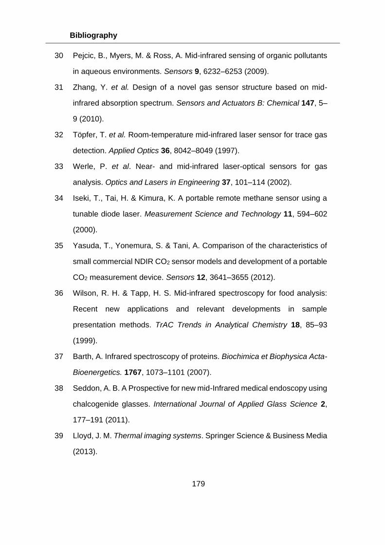
Bibliography
179
30 Pejcic, B., Myers, M. & Ross, A. Mid-infrared sensing of organic pollutants
in aqueous environments. Sensors 9, 6232–6253 (2009).
31 Zhang, Y. et al. Design of a novel gas sensor structure based on mid-
infrared absorption spectrum. Sensors and Actuators B: Chemical 147, 5–
9 (2010).
32 Töpfer, T. et al. Room-temperature mid-infrared laser sensor for trace gas
detection. Applied Optics 36, 8042–8049 (1997).
33 Werle, P. et al. Near- and mid-infrared laser-optical sensors for gas
analysis. Optics and Lasers in Engineering 37, 101–114 (2002).
34 Iseki, T., Tai, H. & Kimura, K. A portable remote methane sensor using a
tunable diode laser. Measurement Science and Technology 11, 594–602
(2000).
35 Yasuda, T., Yonemura, S. & Tani, A. Comparison of the characteristics of
small commercial NDIR CO2 sensor models and development of a portable
CO2 measurement device. Sensors 12, 3641–3655 (2012).
36 Wilson, R. H. & Tapp, H. S. Mid-infrared spectroscopy for food analysis:
Recent new applications and relevant developments in sample
presentation methods. TrAC Trends in Analytical Chemistry 18, 85–93
(1999).
37 Barth, A. Infrared spectroscopy of proteins. Biochimica et Biophysica Acta-
Bioenergetics. 1767, 1073–1101 (2007).
38 Seddon, A. B. A Prospective for new mid-Infrared medical endoscopy using
chalcogenide glasses. International Journal of Applied Glass Science 2,
177–191 (2011).
39 Lloyd, J. M. Thermal imaging systems. Springer Science & Business Media
(2013).
Bibliography
180
40 Vollmer, M., & Möllmann, K. P. Infrared thermal imaging: fundamentals,
research and applications. John Wiley & Sons. (2017).
41 Walther, M., 256× 256 focal plane array mid-wavelength infrared camera
based on InAs/GaSb short-period superlattices. Journal of Electronic
Materials 34, 722-725 (2005).
42 http://lasp.colorado.edu/~bagenal/3720/CLASS5/5Spectroscopy.html
43 Clayden, J. J., Greeves, N., Warren, S. & Wothers, P. Organic Chemistry.
Oxford University Press (2001).
44 Hester, R. E. & Girling, R. B. Spectroscopy of Biological Molecules. Royal
Society of Chemistry (1991).
45 Socrates, G. Infrared and Raman characteristic group frequencies: tables
and charts. John Wiley & Sons (2004).
46 Silverstein, R. M., Bassler, G. C., & Morrill, T. C. Spectrometric
Identification of Organic Compounds. 4th Edn., John Wiley and Sons
(1981).
47 Stiff-Roberts, A. D., Chakrabarti, S., Pradhan, S., Kochman, B., &
Bhattacharya, P. Raster-scan imaging with normal-incidence, midinfrared
InAs/GaAs quantum dot infrared photodetectors. Applied Physics Letters
80, 3265-3267 (2002).
48 Tsuji, T., Hattori, H., Watanabe, M., & Nagaoka, N. Development of night-
vision system. IEEE Transactions on Intelligent Transportation Systems 3,
203-209 (2002).
49 Starr, J. W., & Lattimer, B. Y. Evaluation of navigation sensors in fire smoke
environments. Fire Technology 50, 1459-1481 (2014).
50 Wong, W. K., Tan, P. N., Loo, C. K., & Lim, W. S. An effective surveillance
system using thermal camera. International Conference on Signal
Acquisition and Processing In 2009, 13-17 (2009).
Bibliography
181
51 Allison, R., Johnston, J., Craig, G., & Jennings, S. Airborne optical and
thermal remote sensing for wildfire detection and monitoring. Sensors 16,
1310 (2016).
52 Francisco, G. L. Amorphous silicon bolometer for fire/rescue. In
Thermosense XXIII. International Society for Optics and Photonics 4360,
138-148 (2001).
53 Yu, B., Qi, L., Ye, J. Z., & Sun, H. Preparation and radar wave absorbing
characterization of bicomponent fibers with infrared camouflage. Journal
of Applied Polymer Science 104, 2180-2186 (2007).
54 Liu, X. F., Lai, Y. K., Huang, J. Y., Al-Deyab, S. S., & Zhang, K. Q.
Hierarchical SiO2@ Bi2O3 core/shell electrospun fibers for infrared
stealth camouflage. Journal of Materials Chemistry C 3, 345-351 (2015).
55 Salihoglu, O. et al. Graphene-based adaptive thermal camouflage. Nano
Letters 18, 4541-4548 (2018).
56 Phan, L., Walkup IV, W. G., Ordinario, D. D., Karshalev, E., Jocson, J. M.,
Burke, A. M., & Gorodetsky, A. A. Reconfigurable infrared camouflage
coatings from a cephalopod protein. Advanced Materials 25, 5621-5625
(2013).
57 Schurig, D., Mock, J. J., Justice, B. J., Cummer, S. A., Pendry, J. B., Starr,
A. F., & Smith, D. R. Metamaterial electromagnetic cloak at microwave
frequencies. Science 314, 977-980 (2006).
58 Landy, N., & Smith, D. R. A full-parameter unidirectional metamaterial
cloak for microwaves. Nature Materials 12, 25 (2013).
59 Ma, H. F., & Cui, T. J. Three-dimensional broadband ground-plane cloak
made of metamaterials. Nature Communications 1, 21 (2010).
60 Zang, X., Shi, C., Li, Z., Chen, L., Cai, B., Zhu, Y., & Zhu, H. Illusion
induced overlapped optics. Optics Express 22, 582-592 (2014).
Bibliography
182
61 Jiang, W. X., Qiu, C. W., Han, T., Zhang, S., & Cui, T. J. Creation of ghost
illusions using wave dynamics in metamaterials. Advanced Functional
Materials 23, 4028-4034 (2013).
62 Smith, D. R., Vier, D. C., Koschny, T., & Soukoulis, C. M. Electromagnetic
parameter retrieval from inhomogeneous metamaterials. Physical Review
E 71, 036617 (2005).
63 Smith, D. R., Schultz, S., Markoš, P., & Soukoulis, C. M. Determination of
effective permittivity and permeability of metamaterials from reflection and
transmission coefficients. Physical Review B 65, 195104 (2002).
64 Liu, R., Cui, T. J., Huang, D., Zhao, B., & Smith, D. R. Description and
explanation of electromagnetic behaviors in artificial metamaterials based
on effective medium theory. Physical Review E 76, 026606 (2007).
65 Simovski, C. R., & Tretyakov, S. A. Local constitutive parameters of
metamaterials from an effective-medium perspective. Physical Review B
75, 195111 (2007).
66 Schurig, D., Mock, J. J., & Smith, D. R. Electric-field-coupled resonators
for negative permittivity metamaterials. Applied Physics Letters 88,
041109 (2006).
67 Zhao, Q. et al. Electrically tunable negative permeability metamaterials
based on nematic liquid crystals. Applied Physics Letters 90, 011112
(2007).
68 Shalaev, V. M. Optical negative-index metamaterials. Nature Photonics 1,
41 (2007).
69 Smith, D. R., Pendry, J. B., & Wiltshire, M. C. Metamaterials and negative
refractive index. Science 305, 788-792 (2004).
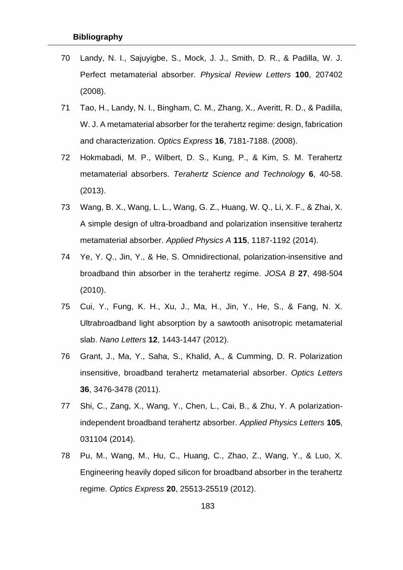
Bibliography
183
70 Landy, N. I., Sajuyigbe, S., Mock, J. J., Smith, D. R., & Padilla, W. J.
Perfect metamaterial absorber. Physical Review Letters 100, 207402
(2008).
71 Tao, H., Landy, N. I., Bingham, C. M., Zhang, X., Averitt, R. D., & Padilla,
W. J. A metamaterial absorber for the terahertz regime: design, fabrication
and characterization. Optics Express 16, 7181-7188. (2008).
72 Hokmabadi, M. P., Wilbert, D. S., Kung, P., & Kim, S. M. Terahertz
metamaterial absorbers. Terahertz Science and Technology 6, 40-58.
(2013).
73 Wang, B. X., Wang, L. L., Wang, G. Z., Huang, W. Q., Li, X. F., & Zhai, X.
A simple design of ultra-broadband and polarization insensitive terahertz
metamaterial absorber. Applied Physics A 115, 1187-1192 (2014).
74 Ye, Y. Q., Jin, Y., & He, S. Omnidirectional, polarization-insensitive and
broadband thin absorber in the terahertz regime. JOSA B 27, 498-504
(2010).
75 Cui, Y., Fung, K. H., Xu, J., Ma, H., Jin, Y., He, S., & Fang, N. X.
Ultrabroadband light absorption by a sawtooth anisotropic metamaterial
slab. Nano Letters 12, 1443-1447 (2012).
76 Grant, J., Ma, Y., Saha, S., Khalid, A., & Cumming, D. R. Polarization
insensitive, broadband terahertz metamaterial absorber. Optics Letters
36, 3476-3478 (2011).
77 Shi, C., Zang, X., Wang, Y., Chen, L., Cai, B., & Zhu, Y. A polarization-
independent broadband terahertz absorber. Applied Physics Letters 105,
031104 (2014).
78 Pu, M., Wang, M., Hu, C., Huang, C., Zhao, Z., Wang, Y., & Luo, X.
Engineering heavily doped silicon for broadband absorber in the terahertz
regime. Optics Express 20, 25513-25519 (2012).
Bibliography
184
79 Zang, X., Shi, C., Chen, L., Cai, B., Zhu, Y., & Zhuang, S. Ultra-broadband
terahertz absorption by exciting the orthogonal diffraction in dumbbell-
shaped gratings. Scientific Reports 5, 8901 (2015).
80 Shi, C., Zang, X. F., Chen, L., Peng, Y., Cai, B., Nash, G. R., & Zhu, Y. M.
Compact broadband terahertz perfect absorber based on multi-
interference and diffraction effects. IEEE Transactions on Terahertz
Science and Technology 6, 40-44. (2015).
81 Shen, X., Yang, Y., Zang, Y., Gu, J., Han, J., Zhang, W., & Jun Cui, T.
(2012). Triple-band terahertz metamaterial absorber: Design, experiment,
and physical interpretation. Applied Physics Letters, 101(15), 154102.
82 Ma, Y., Chen, Q., Grant, J., Saha, S. C., Khalid, A., & Cumming, D. R. A
terahertz polarization insensitive dual band metamaterial absorber. Optics
Letters 36, 945-947 (2011).
83 Lu, D., & Liu, Z. Hyperlenses and metalenses for far-field super-resolution
imaging. Nature Communications 3, 1205 (2012).
84 Aydin, K., Bulu, I., & Ozbay, E. Subwavelength resolution with a negative-
index metamaterial superlens. Applied Physics Letters 90, 254102 (2007).
85 Zhang, X., & Liu, Z. Superlenses to overcome the diffraction limit. Nature
Materials 7, 435 (2008).
86 Liu, Zhaowei. et al. Far-field optical superlens. Nano Letters 7 403-408
(2007).
87 Casse, B. D. F., Lu, W. T., Huang, Y. J., Gultepe, E., Menon, L., & Sridhar,
S. Super-resolution imaging using a three-dimensional metamaterials
nanolens. Applied Physics Letters 96, 023114 (2010).
88 Ma, C., & Liu, Z. A super resolution metalens with phase compensation
mechanism. Applied Physics Letters 96, 183103 (2010).
Bibliography
185
89 Ma, C., & Liu, Z. Focusing light into deep subwavelength using
metamaterial immersion lenses. Optics Express 18, 4838-4844 (2010).
90 Chen, H., Chan, C. T., & Sheng, P. Transformation optics and
metamaterials. Nature Materials 9, 387 (2010).
91 Ergin, T., Stenger, N., Brenner, P., Pendry, J. B., & Wegener, M. Three-
dimensional invisibility cloak at optical wavelengths. Science 328, 337-
339 (2010).
92 Lheurette, E. Metamaterials and Wave Control. Wiley-ISTE (2013).
93 Chen, H. T., Taylor, A. J., & Yu, N. A review of metasurfaces: physics and
applications. Reports on Progress in Physics 79, 076401 (2016).
94 Yu, N., & Capasso, F. Flat optics with designer metasurfaces. Nature
Materials 13, 139 (2014).
95 Zhang, L., Mei, S., Huang, K., & Qiu, C. W. Advances in full control of
electromagnetic waves with metasurfaces. Advanced Optical Materials 4,
818-833 (2016).
96 Holloway, C. L., Kuester, E. F., Gordon, J. A., O'Hara, J., Booth, J., &
Smith, D. R. An overview of the theory and applications of metasurfaces:
The two-dimensional equivalents of metamaterials. IEEE Antennas and
Propagation Magazine 54, 10-35 (2012).
97 Yu, N., Genevet, P., Kats, M. A., Aieta, F., Tetienne, J. P., Capasso, F., &
Gaburro, Z. Light propagation with phase discontinuities: generalized laws
of reflection and refraction. Science 334, 333-337 (2011).
98 Huang, L. et al. Dispersionless phase discontinuities for controlling light
propagation. Nano Letters 12, 5750-5755 (2012).
99 Ding, X. et al. Ultrathin Pancharatnam–Berry metasurface with maximal
cross‐polarization efficiency. Advanced Materials 27, 1195-1200 (2015).
Bibliography
186
100 Ni, X., Emani, N. K., Kildishev, A. V., Boltasseva, A., & Shalaev, V. M.
Broadband light bending with plasmonic nanoantennas. Science 335,
427-427 (2012).
101 Sun, S. et al. High-efficiency broadband anomalous reflection by gradient
meta-surfaces. Nano Letters 12, 6223-6229 (2012).
102 Aieta, F., Genevet, P., Kats, M. A., Yu, N., Blanchard, R., Gaburro, Z., &
Capasso, F. Aberration-free ultrathin flat lenses and axicons at telecom
wavelengths based on plasmonic metasurfaces. Nano Letters 12, 4932-
4936 (2012).
103 Pors, A., Nielsen, M. G., Eriksen, R. L., & Bozhevolnyi, S. I. Broadband
focusing flat mirrors based on plasmonic gradient metasurfaces. Nano
Letters 13, 829-834 (2013).
104 Ni, X., Kildishev, A. V., & Shalaev, V. M. Metasurface holograms for visible
light. Nature Communications 4, 2807 (2013).
105 Huang, L., Chen, X., Mühlenbernd, H., Zhang, H., Chen, S., Bai, B., ... &
Li, J. Three-dimensional optical holography using a plasmonic
metasurface. Nature Communications 4, 2808 (2013).
106 Zheng, G., Mühlenbernd, H., Kenney, M., Li, G., Zentgraf, T., & Zhang, S.
Metasurface holograms reaching 80% efficiency. Nature Nanotechnology
10, 308 (2015).
107 Li, A., Forati, E., & Sievenpiper, D. Study of the electric field enhancement
in resonant metasurfaces. Journal of Optics 19, 125104 (2017).
108 Singh, R., Cao, W., Al-Naib, I., Cong, L., Withayachumnankul, W., &
Zhang, W. Ultrasensitive terahertz sensing with high-Q Fano resonances
in metasurfaces. Applied Physics Letters 105, 171101 (2014).
Bibliography
187
109 Novotny, L., Sánchez, E. J., & Xie, X. S. Near-field optical imaging using
metal tips illuminated by higher-order Hermite–Gaussian beams.
Ultramicroscopy 71, 21-29 (1998).
110 Liu, N., Mesch, M., Weiss, T., Hentschel, M., & Giessen, H. Infrared
perfect absorber and its application as plasmonic sensor. Nano Letters
10, 2342-2348 (2010).
111 Atwater, H. A., & Polman, A. Plasmonics for improved photovoltaic
devices. Nature Materials 9, 205-213 (2010).
112 Sun, Q., Ueno, K., Yu, H., Kubo, A., Matsuo, Y., & Misawa, H. Direct
imaging of the near field and dynamics of surface plasmon resonance on
gold nanostructures using photoemission electron microscopy. Light:
Science & Applications 2, 118. (2013).
113 Dombi, P., Horl, A., Racz, P., Marton, I., Trugler, A., Krenn, J. R., &
Hohenester, U. Ultrafast strong-field photoemission from plasmonic
nanoparticles. Nano Letters 13, 674-678 (2013).
114 Markoš, P., & Soukoulis, C. M. Numerical studies of left-handed materials
and arrays of split ring resonators. Physical Review E 65, 036622 (2002).
115 Wang, H., Sivan, V. P., Mitchell, A., Rosengarten, G., Phelan, P., & Wang,
L. Highly efficient selective metamaterial absorber for high-temperature
solar thermal energy harvesting. Solar Energy Materials and Solar Cells
137, 235-242 (2015).
116 Mulla, B., & Sabah, C. Multiband metamaterial absorber design based on
plasmonic resonances for solar energy harvesting. Plasmonics 11, 1313-
1321 (2016).
117 Zhang, Y. et al. Broadband diffuse terahertz wave scattering by flexible
metasurface with randomized phase distribution. Scientific Reports 6,
26875 (2016).
Bibliography
188
118 Liu, N., Mesch, M., Weiss, T., Hentschel, M., & Giessen, H. Infrared
perfect absorber and its application as plasmonic sensor. Nano Letters
10, 2342-2348 (2010).
119 Hecht, E. Optics 2nd edition. MA: Addison-Wesley Publishing Company
(1987).
120 Zhu, W., Xiao, F., Kang, M., & Premaratne, M. Coherent perfect
absorption in an all-dielectric metasurface. Applied Physics Letters 108,
121901 (2016).
121 Feng, S., & Halterman, K. Coherent perfect absorption in epsilon-near-
zero metamaterials. Physical Review B 86, 165103 (2012).
122 Shrekenhamer, D., Chen, W. C., & Padilla, W. J. Liquid crystal tunable
metamaterial absorber. Physical Review Letters 110, 177403 (2013).
123 Zhao, J., Cheng, Q., Chen, J., Qi, M. Q., Jiang, W. X., & Cui, T. J. A
tunable metamaterial absorber using varactor diodes. New Journal of
Physics 15, 043049 (2013).
124 Zhang, Y., Feng, Y., Zhu, B., Zhao, J., & Jiang, T. Graphene based
tunable metamaterial absorber and polarization modulation in terahertz
frequency. Optics Express 22, 22743-22752 (2014).
125 Yu, N., Aieta, F., Genevet, P., Kats, M. A., Gaburro, Z., & Capasso, F. A
broadband, background-free quarter-wave plate based on plasmonic
metasurfaces. Nano Letters 12, 6328-6333 (2012).
126 Decker, M. et al. High‐efficiency dielectric Huygens’ surfaces. Advanced
Optical Materials 3, 813-820 (2015).
127 Kim, M., Wong, A. M., & Eleftheriades, G. V. Optical Huygens’
metasurfaces with independent control of the magnitude and phase of the
local reflection coefficients. Physical Review X 4, 041042 (2014).
Bibliography
189
128 Monticone, F., Estakhri, N. M., & Alù, A. Full control of nanoscale optical
transmission with a composite metascreen. Physical Review Letters 110,
203903 (2013).
129 Qin, F. et al. Hybrid bilayer plasmonic metasurface efficiently manipulates
visible light. Science Advances 2, e1501168 (2016).
130 de Galarreta, C. R. et al. Nonvolatile Reconfigurable Phase-Change
Metadevices for Beam Steering in the Near Infrared. Advanced Functional
Materials 28, 1704993 (2018).
131 Gholipour, B., Zhang, J., MacDonald, K. F., Hewak, D. W., & Zheludev, N.
I. An all‐optical, non‐volatile, bidirectional, phase‐change meta‐
switch. Advanced Materials 25, 3050-3054 (2013).
132 Chen, H. T., Padilla, W. J., Zide, J. M., Gossard, A. C., Taylor, A. J., &
Averitt, R. D. Active terahertz metamaterial devices. Nature 444, 597
(2006).
133 Liu, M. et al. A graphene-based broadband optical modulator. Nature 474,
64 (2011).
134 Manjappa, M., Pitchappa, P., Singh, N., Wang, N., Zheludev, N. I., Lee,
C., & Singh, R. Reconfigurable MEMS Fano metasurfaces with multiple-
input–output states for logic operations at terahertz frequencies. Nature
Communications 9, 4056 (2018).
135 Goldflam, M. D. et al. Reconfigurable gradient index using VO2 memory
metamaterials. Applied Physics Letters 99, 044103 (2011).
Bibliography
190
136 Balandin, A. A., Ghosh, S., Bao, W., Calizo, I., Teweldebrhan, D., Miao,
F., & Lau, C. N. Superior thermal conductivity of single-layer graphene
Nano Letters 8, 902-907 (2008).
137 Pop, E., Varshney, V., & Roy, A. K. Thermal properties of graphene:
Fundamentals and applications. MRS Bulletin 37, 1273-1281 (2012).
138 Shahil, K. M., & Balandin, A. A. Thermal properties of graphene and
multilayer graphene: Applications in thermal interface materials. Solid
State Communications 152, 1331-1340 (2012).
139 Lee, C., Wei, X., Kysar, J. W., & Hone, J. Measurement of the elastic
properties and intrinsic strength of monolayer graphene. Science 321,
385-388 (2008).
140 Frank, I. W., Tanenbaum, D. M., van der Zande, A. M., & McEuen, P. L.
Mechanical properties of suspended graphene sheets. Journal of Vacuum
Science & Technology B: Microelectronics and Nanometer Structures
Processing, Measurement, and Phenomena 25, 2558-2561 (2007).
141 Novoselov, K. S. et al. Electric field effect in atomically thin carbon films.
Science 306, 666-669 (2004).
142 Novoselov, K. S. et al. Two-dimensional gas of massless Dirac fermions
in graphene. Nature 438, 197 (2005).
143 Neto, A. C., Guinea, F., Peres, N. M., Novoselov, K. S., & Geim, A. K. The
electronic properties of graphene. Reviews of Modern Physics 81, 109
(2009).
144 Semenoff, G. W. Condensed-matter simulation of a three-dimensional
anomaly. Physical Review Letters 53, 2449 (1984).
145 Dirac, P.A.M. Principles of Quantum Mechanics. International Series of
Monographs on Physics (4th ed.). Oxford University Press (1982)
Bibliography
191
146 Zhang, Y., Tan, Y. W., Stormer, H. L., & Kim, P. Experimental observation
of the quantum Hall effect and Berry's phase in graphene. Nature 438,
201 (2005).
147 Novoselov, K. S. et al. Room-temperature quantum Hall effect in
graphene. Science 315, 1379-1379 (2007).
148 Young, A. F., & Kim, P. Quantum interference and Klein tunnelling in
graphene heterojunctions. Nature Physics 5, 222 (2009).
149 Katsnelson, M. I., Novoselov, K. S., & Geim, A. K. Chiral tunnelling and
the Klein paradox in graphene. Nature Physics 2, 620 (2006).
150 Cheianov, V. V., Fal'ko, V., & Altshuler, B. L. The focusing of electron flow
and a Veselago lens in graphene pn junctions. Science 315, 1252-1255
(2007).
151 Liu, H., Liu, Y., & Zhu, D. Chemical doping of graphene. Journal of
Materials Chemistry 21, 3335-3345 (2011).
152 Fang, T., Konar, A., Xing, H., & Jena, D. Carrier statistics and quantum
capacitance of graphene sheets and ribbons. Applied Physics Letters 91,
092109 (2007).
153 Das, A. et al. Monitoring dopants by Raman scattering in an
electrochemically top-gated graphene transistor. Nature Nanotechnology
3, 210 (2008).
154 Ju, L. et al. Graphene plasmonics for tunable terahertz metamaterials.
Nature Nanotechnology 6, 630 (2011).
155 Chen, J. et al. Optical nano-imaging of gate-tunable graphene plasmons.
Nature 487, 77 (2012).
156 Fang, Z. et al. Gated tunability and hybridization of localized plasmons in
nanostructured graphene. ACS Nano 7, 2388-2395 (2013).
Bibliography
192
157 Liu, P. Q., Luxmoore, I. J., Mikhailov, S. A., Savostianova, N. A., Valmorra,
F., Faist, J., & Nash, G. R. Highly tunable hybrid metamaterials employing
split-ring resonators strongly coupled to graphene surface plasmons.
Nature Communications 6, 8969 (2015).
158 Luxmoore, I. J., Liu, P. Q., Li, P., Faist, J., & Nash, G. R. Graphene–
metamaterial photodetectors for integrated infrared sensing. ACS
Photonics 3, 936-941 (2016).
159 Vakil, A. Transformation optics using graphene: one-atom-thick optical
devices based on graphene. PhD dissertation (2012).
160 Luxmoore, I. J., Gan, C. H., Liu, P. Q., Valmorra, F., Li, P., Faist, J., &
Nash, G. R. Strong coupling in the far-infrared between graphene
plasmons and the surface optical phonons of silicon dioxide. ACS
Photonics 1, 1151-1155 (2014).
161 Geim, A. K., & Novoselov, K. S. The rise of graphene. Nature Materials 6,
183-191 (2007).
162 Hanson, G. W. Dyadic Green’s functions and guided surface waves for a
surface conductivity model of graphene. Journal of Applied Physics 103,
064302 (2008).
163 Liu, C., Bai, Y., Zhou, J., Zhao, Q., & Qiao, L. A review of graphene
plasmons and its combination with metasurface. Journal of the Korean
Ceramic Society 54, 349-365 (2017).
164 Dayal, G., Chin, X. Y., Soci, C., & Singh, R. High‐Q Plasmonic Fano
Resonance for Multiband Surface‐Enhanced Infrared Absorption of
Molecular Vibrational Sensing. Advanced Optical Materials 5, 1600559
(2017).
Bibliography
193
165 Koppens, F. H., Chang, D. E., & Garcia de Abajo, F. J. Graphene
plasmonics: a platform for strong light–matter interactions. Nano Letters
11, 3370-3377 (2011).
166 Rodrigo, D., Limaj, O., Janner, D., Etezadi, D., De Abajo, F. J. G., Pruneri,
V., & Altug, H. Mid-infrared plasmonic biosensing with graphene. Science
349, 165-168 (2015).
167 Brar, V. W., Jang, M. S., Sherrott, M., Lopez, J. J., & Atwater, H. A. Highly
confined tunable mid-infrared plasmonics in graphene nanoresonators.
Nano Letters 13, 2541-2547 (2013).
168 Freitag, M., Low, T., Martin-Moreno, L., Zhu, W., Guinea, F., & Avouris, P.
Substrate-sensitive mid-infrared photoresponse in graphene. ACS Nano
8, 8350-8356 (2014).
169 Brar, V. W. et al. Hybrid surface-phonon-plasmon polariton modes in
graphene/monolayer h-BN heterostructures. Nano letters 14, 3876-3880
(2014).
170 Shi, S. F. et al. Optimizing broadband terahertz modulation with hybrid
graphene/metasurface structures. Nano Letters 15, 372-377 (2014).
171 Steinhögl, W., Schindler, G., Steinlesberger, G., Traving, M., &
Engelhardt, M. Comprehensive study of the resistivity of copper wires with
lateral dimensions of 100 nm and smaller. Journal of Applied Physics 97,
023706 (2005).
172 Balandin, A. A., Ghosh, S., Nika, D. L., & Pokatilov, E. P. Thermal
conduction in suspended graphene layers. Fullerenes, Nanotubes, and
Carbon Nanostructures 18, 474-486 (2010).
173 Lindsay, L., Broido, D. A., & Mingo, N. Flexural phonons and thermal
transport in graphene. Physical Review B 82, 115427 (2010).
Bibliography
194
174 Li, Q. Y., Xia, K., Zhang, J., Zhang, Y., Li, Q., Takahashi, K., & Zhang, X.
Measurement of specific heat and thermal conductivity of supported and
suspended graphene by a comprehensive Raman optothermal method.
Nanoscale 9, 10784-10793 (2017).
175 Barnard, H. R., Zossimova, E., Mahlmeister, N. H., Lawton, L. M.,
Luxmoore, I. J., & Nash, G. R. Boron nitride encapsulated graphene
infrared emitters. Applied Physics Letters 108, 131110 (2016).
176 Kim, Y. D. et al. Bright visible light emission from graphene. Nature
Nanotechnology 10, 676 (2015).
177 Freitag, M., Chiu, H. Y., Steiner, M., Perebeinos, V., & Avouris, P. Thermal
infrared emission from biased graphene. Nature Nanotechnology 5, 497
(2010).
178 Bae M-H, Islam S, Dorgan V E and Pop E. Scaling of High-Field Transport
and Localized Heating in Graphene Transistors. ACS Nano 5,7936–44
(2011)
179 Monk, P. Finite element methods for Maxwell's equations. Oxford
University Press (2003).
180 Ŝolín, P. Partial differential equations and the finite element method. John
Wiley & Sons (2005).
181 Causon, D. M., & Mingham, C. G. Introductory finite difference methods
for PDEs. Bookboon (2010).
182 Harrington, R. F. Field Computation by Moment Methods. Wiley-IEEE
Press (1993).
183 Weiland, T. A discretization model for the solution of Maxwell's equations
for six-component fields. Archiv Elektronik und Uebertragungstechnik 31,
116-120 (1977).
Bibliography
195
184 Christ, A., & Hartnagel, H. L. (1987). Three-dimensional finite-difference
method for the analysis of microwave-device embedding. IEEE
Transactions on Microwave Theory and Techniques 35, 688-696 (1987).
185 https://en.wikipedia.org/wiki/Computational_electromagnetics
186 Courant, R. Variational methods for the solution of problems of equilibrium
and vibrations. Bulletin of the American Mathematical Society 49, 1-23
(1943).
187 Yee, K. Numerical solution of initial boundary value problems involving
Maxwell's equations in isotropic media. IEEE Transactions on Antennas
and Propagation 14, 302-307 (1966).
188 https://en.wikipedia.org/wiki/Finite-difference_time-domain_method
189 https://www.agilent.com/cs/library/applications/application-refractive-
index-cary-5000-uv-vis-5994-0052en-us-agilent.pdf
190 https://kb.lumerical.com/ref_sim_obj_mesh_refinement.html
191 Obraztsov, A. N. Chemical vapour deposition: making graphene on a large
scale. Nature Nanotechnology 4, 212 (2009).
192 Mattevi, C., Kim, H., & Chhowalla, M. A review of chemical vapour
deposition of graphene on copper. Journal of Materials Chemistry 21,
3324-3334 (2011).
193 Muñoz, R., & Gómez‐Aleixandre, C. Review of CVD synthesis of
graphene. Chemical Vapor Deposition 19, 297-322 (2013).
194 Suk, J. W., et al. Transfer of CVD-grown monolayer graphene onto
arbitrary substrates. ACS Nano 5, 6916-6924 (2011).
195 Inkson, B. J. Scanning electron microscopy (SEM) and transmission
electron microscopy (TEM) for materials characterization. In Materials
characterization using nondestructive evaluation (NDE) methods.
Woodhead Publishing (2016).
Bibliography
196
196 Eaton, P., & West, P. Atomic force microscopy. Oxford University Press
(2010).
197 Software downloaded from http://gwyddion.net/
198 Bruker Vertex Series Brochure
199 https://www.bruker.com/products/infrared-near-infrared-and-raman-
spectroscopy/ft-ir/ft-ir-accessories/platinum-atr/overview.html
200 Hildenbrand, J. et al. Micromachined mid-infrared emitter for fast transient
temperature operation for optical gas sensing systems. IEEE Sensors
Journal 10, 353–362 (2010).
201 Pusch, A. et al. A highly efficient CMOS nanoplasmonic crystal enhanced
slow-wave thermal emitter improves infrared gas-sensing devices.
Scientific. Reports 5, 17451 (2015).
202 Bauer, D., Heeger, M., Gebhard, M. & Benecke, W. Design and fabrication
of a thermal infrared emitter. Sensors and Actuators A: Physical 55, 57–
63 (1996).
203 MacIsaac, D., Kanner, G. & Anderson, G. Basic physics of the
incandescent lamp (lightbulb). The Physics Teacher 37, 520–525 (1999).
204 Yao, Y., Hoffman, A. J. & Gmachl, C. F. Mid-infrared quantum cascade
lasers. Nature Photonics 6, 432–439 (2012).
205 Haigh, M. K. et al. Mid-infrared AlxIn1-xSb light-emitting diodes. Applied
Physics. Letters 90, 231116 (2007).
Bibliography
197
206 Nash, G. R. et al. Mid-Infrared AlxIn1-xSb Light-Emitting Diodes and
Photodiodes for Hydrocarbon Sensing. IEEE Sensors Journal. 9, 1240–
1243 (2009).
207 Hildenbrand, J. et al. Fast transient temperature operating micromachined
emitter for mid-infrared optical gas sensing systems: design, fabrication,
characterization and optimization. Microsystem Technologies 16, 745–
754 (2010).
208 Ban, D. et al. Optimized GaAs∕ AlGaAs light-emitting diodes and high
efficiency wafer-fused optical up-conversion devices. Journal of Applied
Physics 96, 5243-5248 (2004).
209 Dror, B., Zheng, Y., Agrawal, M., Radhakrishnan, K., Orenstein, M., &
Bahir, G. Mid-Infrared GaN/AlGaN Quantum Cascade Detector Grown on
Silicon. IEEE Electron Device Letters 40, 263-266 (2019).
210 Geim, A. K. Graphene: status and prospects. Science 324, 1530–1534
(2009).
211 Bonaccorso, F., Sun, Z., Hasan, T. & Ferrari, A. C. Graphene Photonics
and Optoelectronics. Nature Photonics 4, 611–622 (2010).
212 Campos-Delgado, J. et al. Thermal stability studies of CVD-grown
graphene nanoribbons: Defect annealing and loop formation. Chemical
Physics Letters 469, 177–182 (2009).
Bibliography
198
213 Dorin, B. A., & Winnie, N. Y. Two-mode division multiplexing in a silicon-
on-insulator ring resonator. Optics Express 22, 4547-4558 (2014).
214 Papasimakis, N., Fu, Y. H., Fedotov, V. A., Prosvirnin, S. L., Tsai, D. P.,
& Zheludev, N. I. Metamaterial with polarization and direction insensitive
resonant transmission response mimicking electromagnetically induced
transparency. Applied Physics Letters 94, 211902 (2009)
215 Hsieh, L. H., & Chang, K. Equivalent lumped elements G, L, C,and
unloaded Q's of closed- and open-loop ring resonators. IEEE
Transactions on Microwave Theory and Techniques 50, 453–460 (2002).
216 Madelung, O., Rössler, U., & Schulz, M. Group IV Elements, IV-IV and III-
V Compounds. Part a - Lattice Properties. Springer (Berlin Heidelberg,
2001).
217 Palik, E. D. Handbook of optical constants of solids. Academic press
(1998).
218 Robitaille, P. M. Kirchhoff’s law of thermal emission: 150 years. Progress
in Physics 4, 3-13 (2009).
219 Yang, X., et al. Far‐Field Spectroscopy and Near‐Field Optical Imaging of
Coupled Plasmon–Phonon Polaritons in 2D van der Waals
Heterostructures. Advanced Materials 28, 2931-2938 (2016).
Bibliography
199
220 Meier, R. Handbook of Vibrational Spectroscopy. Chalmers, J., Griffiths,
P. R., Eds., John Wiley & Sons Ltd. (2003).
221 Ataka, K., Kottke, T., Heberle, & J. Thinner, smaller, faster: IR techniques
to probe the functionality of biological and biomimetric systems.
Angewandte Chemie International Edition 49, 5416–5424 (2010).
222 Haris, P. I., & Severcan, F. FTIR spectroscopic characterization of protein
structure in aqueous and non-aqueous media. Journal of Molecular
Catalysis B: Enzymatic 7, 207-221 (1999).
223 Fahrenfort, J. Attenuated total reflection: A new principle for the production
of useful infra-red reflection spectra of organic compounds. Spectrochim
Acta 17, 698-709 (1961).
224 Dunuwila, D. D., Carroll II, L. B., & Berglund, K.A. An investigation of the
applicability of attenuated total reflection infrared spectroscopy for
measurement of solubility and supersaturation of aqueous citric acid
solutions. Journal of Crystal Growth 137, 561-568. (1994)
225 Iwaki, M., Cotton, N. P., Quirk, P. G., Rich, P. R., & Jackson, J. B.
Molecular recognition between protein and nicotinamide dinucleotide in
intact, proton-translocating transhydrogenase studied by ATR-FTIR
spectroscopy. Journal of the American Chemical Society 128, 2621–2629
(2006).
Bibliography
200
226 Brown, L. V., et al. Fan-shaped gold nanoantennas above reflective
substrates for surface-enhanced infrared absorption (SEIRA). Nano
Letters 15, 1272-1280 (2015).
227 Huck, C. et al. Plasmonic enhancement of infrared vibrational signals:
nanoslits versus nanorods. ACS Photonics 2,1489-1497 (2015.).
228 Rodrigo, D. et al. Mid-infrared plasmonic biosensing with graphene.
Science 349, 165–168 (2015).
229 Cerjan, B., Yang, X., Nordlander, P., & Halas, N. J., Asymmetric aluminum
antennas for self-calibrating surface-enhanced infrared absorption
spectroscopy. ACS Photonics 3, 354-360 (2016).
230 Verger, F. et al. Surface enhanced infrared absorption by nanoantenna on
chalcogenide glass substrates. Applied Physics Letters 106(7), 073103
(2015).
231 Umari, P., Pasquarello, A., Dal Corso, A. Raman scattering intensities in
α-quartz: a first-principles investigation. Physics Review B 63, 094305
(2001).
232 Fratini, S., Guinea, F. Substrate-limited electron dynamics in Graphene.
Physics Review B 77, 195414 (2008).
233 https://webbook.nist.gov/cgi/cbook.cgi?ID=C123864&Type=IR-SPEC
Bibliography
201
234 https://webbook.nist.gov/cgi/cbook.cgi?ID=C112801&Type=IR-
SPEC&Index=1
235 Cui, T. J., Qi, M. Q., Wan, X., Zhao, J., & Cheng, Q. Coding metamaterials,
digital metamaterials and programmable metamaterials. Light: Science &
Applications 3, e218 (2014).
236 Li, L. et al. Electromagnetic reprogrammable coding-metasurface
holograms. Nature Communications 8, 197 (2017).
237 Wang, L., Li, L., Li, Y., Zhang, H. C., & Cui, T. J. Single-shot and single-
sensor high/super-resolution microwave imaging based on metasurface.
Scientific. Reports 6, 26959 (2016).
238 Lyakh, A., Maulini, R., Tsekoun, A., Go, R., & Patel, C. K. N. Intersubband
absorption of quantum cascade laser structures and its application to laser
modulation. Applied Physics Letters 92, 211108 (2008).
239 Roy, T., et al Dynamic metasurface lens based on MEMS technology. APL
Photonics 3, 021302 (2018).
240 Bolotin, K., et al Ultrahigh electron mobility in suspended graphene. Solid
Solid State Communications 146, 351–355 (2008).
241 Novoselov K. S., et al. A roadmap for graphene. Nature 490, 192–200
(2012).
Bibliography
202
242 Andryieuski, A., & Lavrinenko, A. V. Graphene metamaterials based
tunable terahertz absorber: effective surface conductivity approach.
Optics Express 21, 9144-9155 (2013).
243 He, X., Liu, F., Lin, F., & Shi, W. Graphene patterns supported terahertz
tunable plasmon induced transparency. Optics Express 26, 9931-9944
(2018).
244 Zhang, Y. et al. Independently tunable dual-band perfect absorber based
on graphene at mid-infrared frequencies. Scientific Reports 5, 18463
(2015).
245 Huang, H. et al. Design of broadband graphene-metamaterial absorbers
for permittivity sensing at mid-infrared regions. Scientific Reports 8, 4183
(2018).
246 Cai, Y. et al. Enhanced spatial near-infrared modulation of graphene-
loaded perfect absorbers using plasmonic nanoslits. Optics Express
23(25), 32318-32328 (2015).
247 Sun, C., Dong, Z., Si, J., & Deng, X., Independently tunable dual-band
plasmonically induced transparency based on hybrid metal-graphene
metamaterials at mid-infrared frequencies. Optics Express 25(2), 1242-
1250 (2017).
Bibliography
203
248 Serway, R. A., & Jewett, J. W., Principles of physics (2nd Ed.). Fort Worth,
TX: Saunders College Pub (1998).
249 Kim, S. et al. Electronically tunable extraordinary optical transmission in
graphene plasmonic ribbons coupled to subwavelength metallic slit
arrays. Nature Communications 7, 12323 (2016).
250 Chen, K. et al. A reconfigurable active huygens' metalens. Advanced
Materials 29, 1606422 (2017).
251 Ee, H. S., & Agarwal, R. Tunable metasurface and flat optical zoom lens
on a stretchable substrate. Nano Letters 16, 2818-2823 (2016).
252 Iyer, P. P., Pendharkar, M., & Schuller, J. A. Electrically reconfigurable
metasurfaces using heterojunction resonators. Advanced Optical
Materials 4, 1582-1588 (2016).
253 Wang, Q. et al. Optically reconfigurable metasurfaces and photonic
devices based on phase change materials. Nature Photonics 10(1), 60
(2016).
254 Zhu, Z., Evans, P. G., Haglund Jr, R. F., & Valentine, J. G. Dynamically
reconfigurable metadevice employing nanostructured phase-change
materials. Nano Letters 17, 4881-4885 (2017).
255 Bohren, C. F., & Huffman, D. R. Absorption and scattering of light by
small particles. John Wiley & Sons (2008).
256 Ismach, A. et al. Direct chemical vapor deposition of graphene on
dielectric surfaces. Nano Letters 10, 1542-1548 (2010).

Bibliography
204