
Metal photocathodes for NCRF electron guns Sonal Mistry Loughborough University Supervisor: Michael...
17
Metal photocathodes for NCRF electron guns Sonal Mistry Loughborough University Supervisor: Michael Cropper (Loughborough University) Industrial Supervisor: Reza Valizadeh (ASTeC, STFC, Daresbury Laboratory) Boris Militsyn (ASTeC, STFC, Daresbury Laboratory) 1
-
Upload
brittany-riley -
Category
Documents
-
view
217 -
download
0
Transcript of Metal photocathodes for NCRF electron guns Sonal Mistry Loughborough University Supervisor: Michael...
Metal photocathodes for NCRF electron guns
Sonal Mistry Loughborough University
Supervisor:
Michael Cropper (Loughborough University)Industrial Supervisor:
Reza Valizadeh (ASTeC, STFC, Daresbury Laboratory)Boris Militsyn (ASTeC, STFC, Daresbury Laboratory)
1
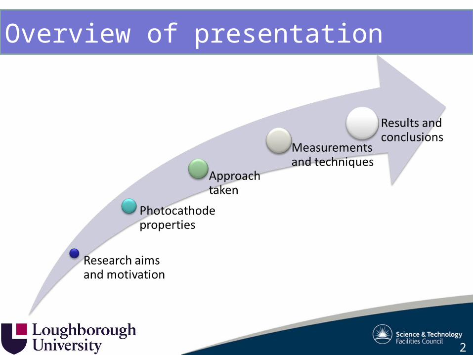
Overview of presentation
2
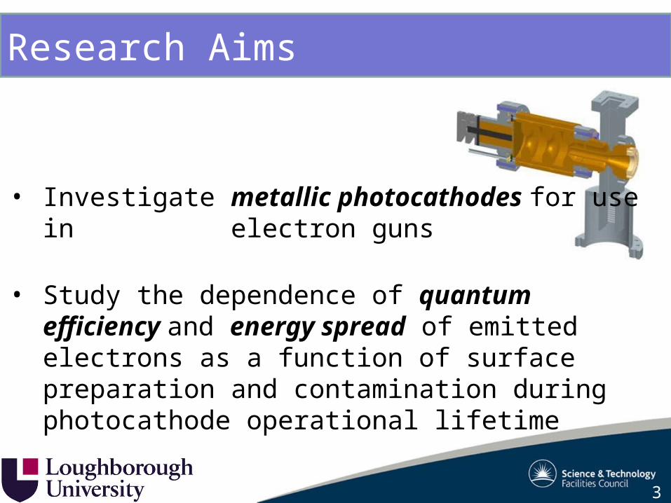
Research Aims
• Investigate metallic photocathodes for use in electron guns
• Study the dependence of quantum efficiency and energy spread of emitted electrons as a function of surface preparation and contamination during photocathode operational lifetime
3

Motivations for Research
• Interest in investigating alternative metal to copper with better properties
• Investigate applicability of metals to deliver ultra high beams
VELA• VELA (Versatile electron linear accelerator)• Photoinjector consists of 2.5 cell S-band RF gun• Cu photocathodes integrated onto copper cavity
4
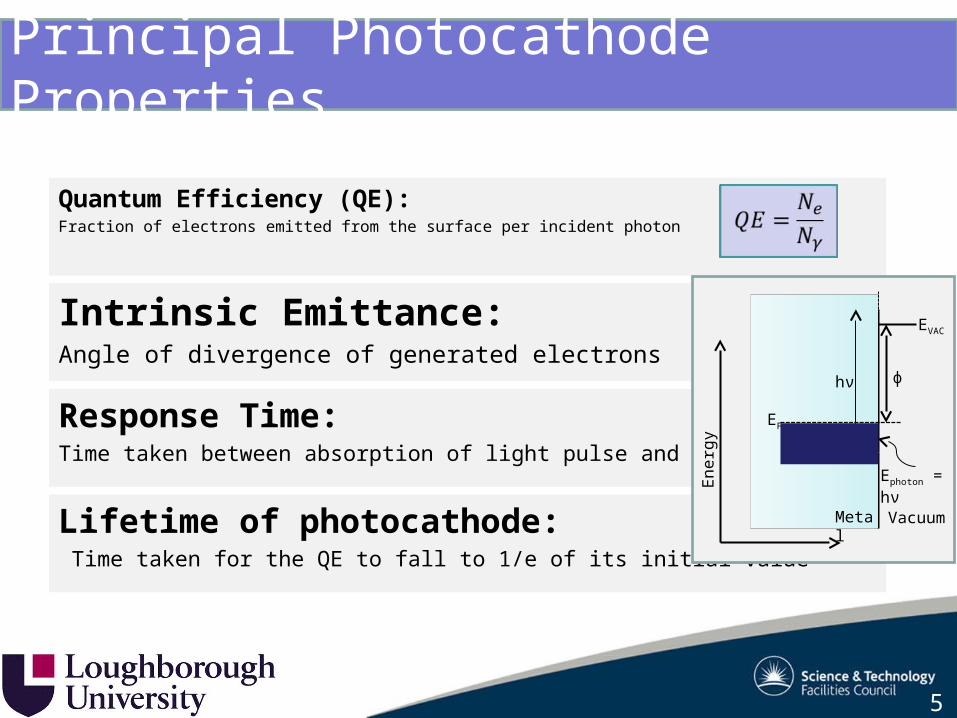
Principal Photocathode Properties
Quantum Efficiency (QE): Fraction of electrons emitted from the surface per incident photon
Intrinsic Emittance: Angle of divergence of generated electrons
Response Time: Time taken between absorption of light pulse and photoemission
Lifetime of photocathode: Time taken for the QE to fall to 1/e of its initial value
5
Ener
gy
Metal Vacuum
e-
hν
EF
EVAC
ɸ
Ephoton = hν

Approach
• Investigate differences between single and polycrystalline samples
7
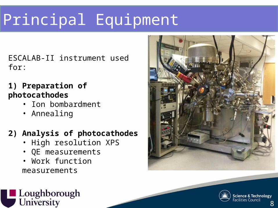
Principal Equipment
ESCALAB-II instrument used for:
1) Preparation of photocathodes• Ion bombardment • Annealing
2) Analysis of photocathodes• High resolution XPS• QE measurements • Work function measurements
8
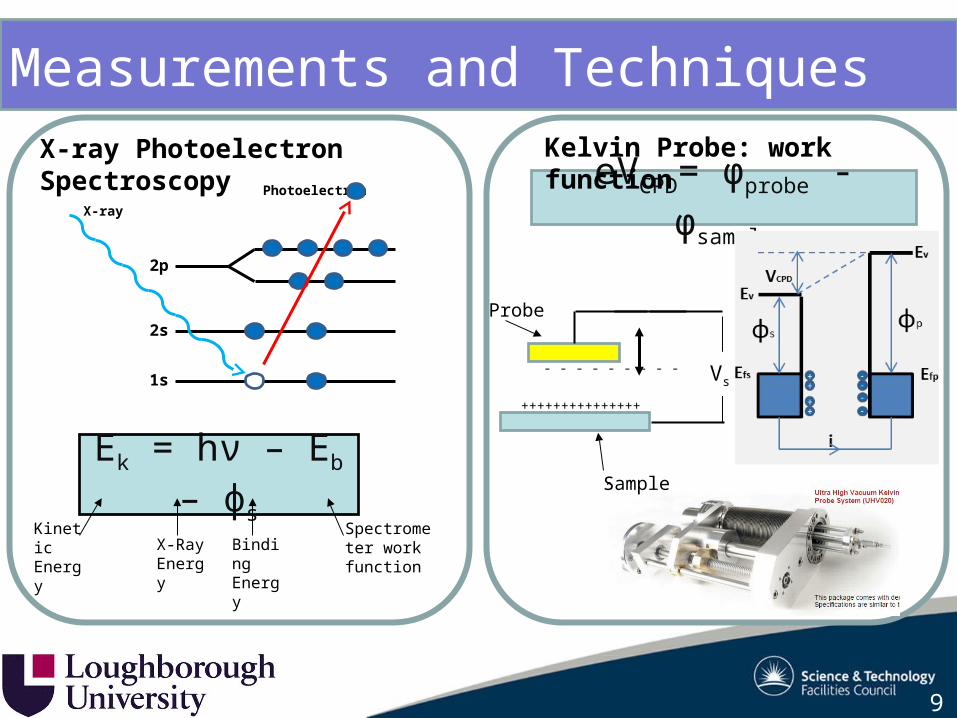
Measurements and Techniques
Photoelectron
1s
2s
2p
X-ray
X-ray Photoelectron Spectroscopy
Ek = hν – Eb – ɸs
Kinetic Energy X-Ray
EnergyBinding Energy
Spectrometer work function
9
eVCPD= φprobe - φsample
Kelvin Probe: work function
Sample
Probe
Vs
+++++++++++++++
- - - - - - - - -

QE measured using UV LED/ UV LASER• QE measurements comprise
• a LED source- 265 nm (4.65 eV) light and a pico-ammeter to measure photocurrent.
• photodiode used to measure LED power
• QE suggests how much current can be extracted from a cathode and as such is an indication of the potential beam current.
hν
e-
e-
e-e-e-
11
Ener
gy
Metal Vacuum
e-
hν
EF
EVAC
ɸ
Ephoton = hν
• UV LASER source which offers higher intensity at 266 nm
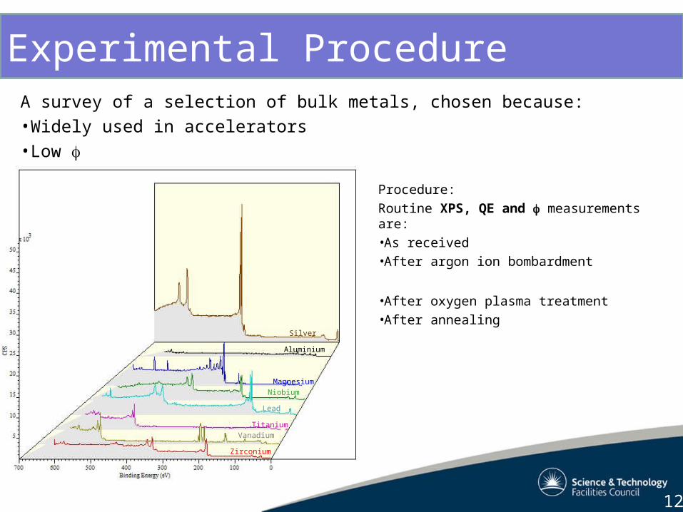
A survey of a selection of bulk metals, chosen because:•Widely used in accelerators•Low
Experimental Procedure
Zirconium
Vanadium
Titanium
Lead
Niobium
Magnesium
Aluminium
Silver
12
Procedure: Routine XPS, QE and measurements are:•As received•After argon ion bombardment
•After oxygen plasma treatment•After annealing
Metal QE XPS (%)O 1s C 1s
Measured (eV)
Al Received Ar+ sputter
9.5E-62.2E-5
36.8 38.313.4 17.4
4.0224.914
Ag Received Ar+ sputter
8.5E-65.1E-5
0 59.4 0 0
5.0885.111
Cu Received Ar+ sputter
5.0E-61.1E-5
32.9 66.2 0 0
5.3535.316
Mg Received Ar+ sputter
6.0E-61.7E-3
35.2 52.340.0 0
3.3903.372
Mo Received Ar+ sputter
1.47E-72.48E-6
24.2 64.97.8 17.8
5.0715.178
Results: Bulk metals Ar+ sputterMetal QE XPS (%)
O 1s C 1sMeasured (eV)
Nb Received Ar+ sputter
3.9E-71.9E-4
47.8 48.616.2 21.0
5.3014.713
Pb Received Ar+ sputter
2.9E-52.4E-4
43.9 34.8 0 0
4.5734.660
Ti Received Ar+ sputter
03.3E-4
39.2 53.614.6 16.8
4.7464.467
V Received Ar+ sputter
1.4E-62.2E-5
45.7 45.925.0 0
5.5064.999
Zr Received Ar+ sputter
3.88E-62.89E-4
48.4 44.114.4 0
4.4344.263
15

Metal QE XPS (%)O 1s C 1s
(eV)
Cu O2 plasma Anneal 250°C (0.5 hr)
01.6E-4
80.1 3.176.7 6.5
5.6535.716
Nb O2 plasma Anneal 300°C (0.5 hr)
5.21E-71.34E-4
87.5 5.7 80.2 6.3
5.7124.510
Pb O2 plasma Anneal 160°C (0.5 hr) Anneal 200°C (0.5 hr)
3.47E-76.94E-61.67E-5
82.1 7.177.9 10.977.8 9.9
5.6164.3004.473
Metal QE XPS (%)O 1s C 1s
(eV)
Ti O2 plasma Anneal 250°C (0.5 hr) Anneal 250C (24 hr)
06.32E-51.16E-4
87.1 5.188.3 4.579.9 9.0
5.7744.4994.268
Zr O2 plasma Anneal 250°C (0.5 hr) Anneal 250°C (24 hr)
3.82E-76.94E-51.35E-4
78.4 12.483.5 3.974.6 9.8
4.9414.2634.797
Mg O2 plasma Anneal 200°C (0.5 hr) Anneal 200°C (4 hr) Anneal 200°C (24 hr)
3.82E-72.40E-54.90E-57.09E-5
83.5 3.276.8 3.567.8 9.466.7 3.8
4.3963.8693.7373.627
Measurements for Ti, Zr, Mg, Cu, Nb, Pb:O2 Plasma Cleaned for 20 minutes Annealed
Results: Bulk metal O2 plasma cleaned

Metal thin film QE XPS (%)O 1s C 1s
Measured (eV)
Cu Received Heated 250°C Repeat
1.47E-61.14E-41.17E-4
23.5 67.820.2 61.717.9 62.0
5.14354.9144.68
Nb Received Heated 250°C Heated 300°C Ar+ sputter
7.75E-72.45E-55.66E-62.64E-4
63.1 25.361.5 4.355.8 15.99.6 0
4.35334.88595.14014.7703
Results: Thin film metals
• Metal thin films deposited on silicon substrate by magnetron sputtering
• So far only Cu and Nb thin films have been produced
16

Copper thin film compared with bulk sample (½ hour heating at 250°C)
Wide scan XPS Bulk (%) Thin film(%)O 1s 6.1 17.943C 1s none 62.03Cu 2p 93.9 20.027
x 104
2
4
6
8
10
12
14
CPS
1000 800 600 400 200 0
Binding Energy (eV)
Cu 2p1/2
Cu 2p3/2
Auger Lines
Work function (eV)
QE
Bulk 5.234 1.70E-5
Thin Film 4.68 1.17E-4
17

x 103
2
4
6
8
10
12
14
16
18
20
CPS
600 500 400 300 200 100 0Binding Energy (eV)
XPS Bulk (%) Thin film(%)O 1s 16.24 9.57C 1s 20.98 noneNb 3p 62.78 90.43
Niobium thin film compared with bulk sample (Ar+ sputter)
Wide scan
O 1s
Nb 3d5/2
Nb 3d3/2
Nb 3p3/2
Nb 3p1/2
Nb 3s
Work function (eV)
QE
Bulk 4.713 1.9E-4
Thin Film 4.7703 2.64E-4
18
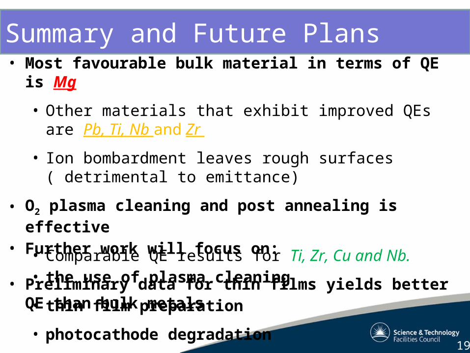
Summary and Future Plans• Most favourable bulk material in terms of QE is Mg
• Other materials that exhibit improved QEs are Pb, Ti, Nb and Zr
• Ion bombardment leaves rough surfaces ( detrimental to emittance)
• O2 plasma cleaning and post annealing is effective
• Comparable QE results for Ti, Zr, Cu and Nb.
• Preliminary data for thin films yields better QE than bulk metals
19
• Further work will focus on:
• the use of plasma cleaning
• thin film preparation
• photocathode degradation

Thank you for your attention
20