Metal-organic framework nanosheets for enhanced ... · spectrum proportional to the fluorescence...
37
1 Metal-organic framework nanosheets for enhanced performance of organic photovoltaic cells Kezia Sasitharan, David G. Bossanyi, Naoum Vaenas, Andrew J. Parnell, Jenny Clark, Ahmed Iraqi, David G. Lidzey, Jonathan A. Foster Supplementary information Table of contents 1. General experimental procedures 2. Syntheses 3. Structural characterisation of MOF (XRD, TGA, FT-IR) 4. Morphological characterisation (AFM, TEM) 5. Opto-electronic characterisation (UV-Vis, CV, PL) 6. Casting of films 7. Device fabrication and testing 8. Transient absorption 9. Charge mobility measurements 10. GI-WAXS 11. AFM- Understanding the morphology of device active layers 12. Spectroscopic ellipsometry 13. References Electronic Supplementary Material (ESI) for Journal of Materials Chemistry A. This journal is © The Royal Society of Chemistry 2020
Transcript of Metal-organic framework nanosheets for enhanced ... · spectrum proportional to the fluorescence...
1
Metal-organic framework nanosheets for enhanced performance of organic
photovoltaic cells
Kezia Sasitharan, David G. Bossanyi, Naoum Vaenas, Andrew J. Parnell, Jenny Clark, Ahmed
Iraqi, David G. Lidzey, Jonathan A. Foster
Supplementary information
Table of contents
1. General experimental procedures
2. Syntheses
3. Structural characterisation of MOF (XRD, TGA, FT-IR)
4. Morphological characterisation (AFM, TEM)
5. Opto-electronic characterisation (UV-Vis, CV, PL)
6. Casting of films
7. Device fabrication and testing
8. Transient absorption
9. Charge mobility measurements
10. GI-WAXS
11. AFM- Understanding the morphology of device active layers
12. Spectroscopic ellipsometry
13. References
Electronic Supplementary Material (ESI) for Journal of Materials Chemistry A.This journal is © The Royal Society of Chemistry 2020

2
1. General experimental procedures
Commercial solvents and reagents were used without further purification. Synthesis of
organic ligands was carried out in dry glassware with a nitrogen overpressure. Solvothermal
synthesis of metal-organic frameworks was undertaken using borosilicate vials with Teflon
faced rubber lined caps.
NMR spectra were recorded on a Bruker Advance DPX 400 spectrometer. Chemical shifts for
1H are reported in ppm on the scale; 1H chemical shifts were referenced to the residual
solvent peak. All coupling constants are reported in Hz. Mass spectra were collected using a
Bruker Reflex III MALDI-TOF spectrometer. Elemental analyses were obtained on a vario
MICRO CHNS elemental analyzer equipped with a thermal conductivity detector. X-Ray
powder diffraction patterns were collected using a Bruker D8 Advance powder diffractometer
equipped with a copper Kα source (λ=1.5418 Å) operating at 40 kV and 40 mA. The instrument
was fitted with an energy-dispersive LYNXEYE detector. Measurements were carried out using
a fixed goniometer stage with a rotating flat plate sample holder. IR spectroscopy was
performed on a Perkin-Elmer Pyris TGA from 30-600°C at 10°C min-1, under a 20 mL min-1
nitrogen flow. UV-Vis absorption spectra were collected on a Cary 5000 UV-Vis-NIR
instrument using a 1 cm internal length quartz cuvette. PL spectra were recorded using a
Horiba FluoroMax spectrofluorometer using 500 nm excitation. The fluorescence emission
was corrected for sample absorption at the excitation wavelength to produce an emission
spectrum proportional to the fluorescence quantum efficiency.
Nanoscopic characterisation was performed using a Bruker Multimode 5 AFM, operating in
soft-tapping mode under ambient conditions. Bruker OTESPA-R3 cantilever were used, with
a drive amplitude and nominal resonance frequency of 20.4 mV and 290 kHz, respectively.
Images were processed using standard techniques with free Gwyddion software. TEM
images were obtained using a JEOL-2010F TEM operated at an accelerated voltage of 200
kV.

3
2. Syntheses
2.1 Synthesis of meso-tetracarboxyphenyl porphyrin (TCPP) ligand
10 mL of pyrrole (98%, light brown solution) was distilled under vacuum at 80°C to give 5 mL
of a clear solution. 4-formylbenzoic acid (3.0 g, 20 mmol) was dissolved in propionic acid (100
mL) and freshly distilled pyrrole (1.4 mL, 20 mmol) was added by syringe. The solution
immediately darkened and was refluxed for 15 hours. The mixture was chilled in a fridge for
10 hours before collection of the solid by vacuum filtration. The solid was washed with hot
water (2 x 20 mL) and dried under vacuum to give the product as a black powder (3.23 g, 4.0
mmol, 80 %). Elemental Analysis calculated for C48H30N4O8: Expected: C, 72.91; H, 3.82; N,
7.09. Found: C, 72.95; H, 4.08; N, 6.82
λmax (nm): 420 (π-π*)
1H-NMR (d6-DMSO) δ/ppm: 8.85 (8H, s, β-pyrrolic H), 8.38 (8H, d, J = 8.0, Ar-H), 8.32 (8H, d, J
= 8.0, Ar-H), -2.95 (2H, s, internal pyrrole NH).
MALDI-TOF: m/z 791.2 ([MH]+)
2.2 Synthesis of bulk Zn2(Zn-TCPP)(DMF)
H2TCPP (7.9 mg, 0.03 mmol), Zn(NO3)2.3H2O (8.9 mg, 0.09 mmol), DMF (1.5 mL) and ethanol
(0.5 mL) were mixed at room temperature and heated at 80°C for 24 hours. Purple crystals
were collected by centrifugation at 4500 RPM for 10 minutes and repeatedly washed in
ethanol until the supernatant became clear (Yield 87%)
Elemental analysis C48H24N4O8Zn3(H2O)4(DMF)3: Expected C, 53.57; H, 4.50; N, 8.33 Found C,
52.76; H, 4.77; N, 8.88.
A slight excess of Zn around the edge of the MOF and possible nitrate counter ions could be
the reason for lower carbon content and higher nitrogen.
2.3 Exfoliation of MOF into MONs
20 mg of Zn2(ZnTCPP) MOF was added to a 10 mL glass vial along with 4 mL of the desired
solvent. The sample was mixed in a vortex mixer for 30 seconds to disperse the sediment. The
samples were sonicated using a Fisherbrand Elmasonic P 30H ultrasonic bath (2.75 L, 380/350

4
W, UNSPSC 42281712) filled with water. Samples were sonicated for 60 min at a frequency of
80 kHz with 100% power and the temperature was thermostatically maintained at 16-20°C
using a steel cooling coil. Sonication was applied using a sweep mode and samples were
rotated through the water using an overhead stirrer to minimise variation due to ultrasound
“hot-spots”. Following sonication, the vials were transferred to centrifuge tubes and
centrifuged at 1500 RPM for 10 minutes to remove non-exfoliated particles.
3. Structural characterisations
10 20 30 40 50
0.00.20.40.60.81.0
10 20 30 40 50
0.00.20.40.60.81.0
Inte
nsi
ty
MONs in Chlorobenzene
2 theta
Bulk MOF
Figure S1 Powder diffraction pattern for as-synthesized Zn2(ZnTCPP) MON in comparison with
the synthesized bulk MOF. The diffraction patterns are in accordance with the previous
reports1

5
TGA
0 200 400 600 8000
10
20
30
40
50
60
70
80
90
100 ZnTCPP
Wei
ght
loss
(%
)
Temperature (oC)
Figure S2 Thermo-gravimetric analysis of Zn2(ZnTCPP)(H2O)4(DMF)3 MOF
Loss of solvent (Calculated 22.89%; Experimental: 22.74%)
4000 3000 2000 100075
80
85
90
95
100
105
Inte
nsi
ty
Wavenumber (cm-1)
Bulk MOF
H2O u (OH str)
DMF u (C-O str)
u (COO symm) Exfoliated MONs
Figure S3 FTIR spectra of Zn2(ZnTCPP) bulk MOF in comparison with exfoliated MONs.
The tyndall scattering observed in the supernatant containing the MONs confirms their
colloidal nature.

6
Figure S4. Tyndall scattering observed in a MON suspension
7
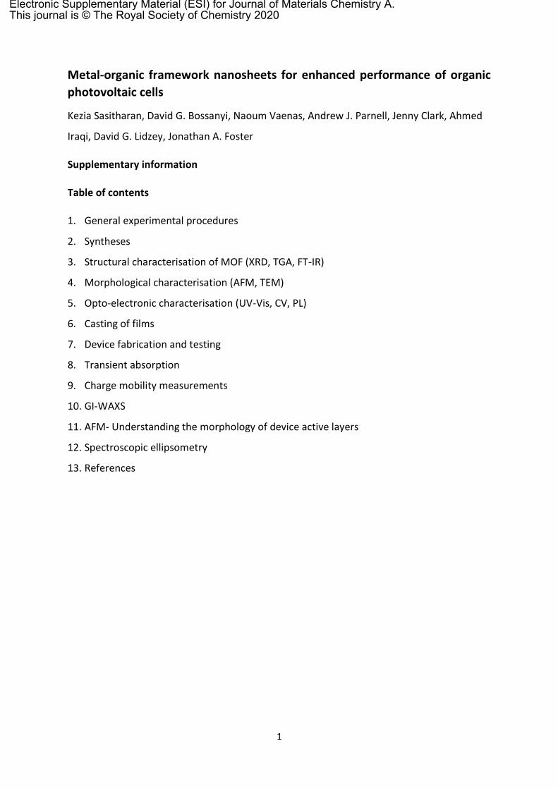
4. Morphological characterisations
4.1 AFM
AFM samples of the nanosheets were prepared through dropping aliquots (typically 2 x 5 µL
drops) of a suspension onto freshly cleaved Mica, which had been stuck to a magnetic,
stainless steel Agar scanning probe microscopy specimen disc for loading into the instrument.
4.2 TEM
4.2 TEM and EELS
Figure S5 AFM topographical images of the nanosheets and the corresponding height profile.

8
Prior to TEM characterisation, the suspension (10uL) of the nanosheets was dropcast onto
holey C-coated Cu grid and allowed for evaporation of the solvent.
Figure S6. HRTEM and corresponding FFT (b) pattern of the MONs; c. Electron energy loss
spectroscopy
5. Opto-electronic characterisation
5.1 UV-Vis in solution state
400 500 600 700 800
0.0
0.2
0.4
0.6
0.8
1.0 Bulk MOF
Exfoliated MONs
No
rmal
ized
Ab
sorp
tio
n
Wavelength (nm)
Figure S7. UV-Vis spectroscopy of suspension of the bulk MOF (in Ethanol) and MONs (in
chlorobenzene); 0.1 mM concentration.
5.2 Cyclic voltammetry
The CV analysis was conducted in an acetonitrile solution containing tetrabutylammonium
perchlorate electrolyte with Ag/Ag+ as the reference electrode and Pt wire as the counter
electrode. The nanosheets were dropcast as films onto the glassy carbon working electrode
e-
eV
-5000
0
5000
10000
15000
20000
25000
e-
0 200 400 600 800
eV
b a c

9
and the measurements were performed under an inert atmosphere of Argon with a scan rate
of 100 mVs-1.
Figure S8 HOMO-LUMO level determination from the CV scan of Zn2(ZnTCPP) MONs
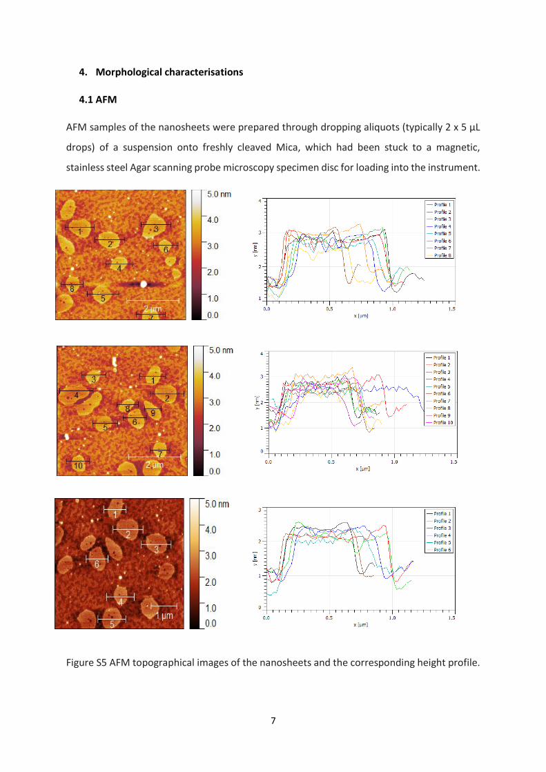
5.3 Thin film UV-Vis for optical band gap evaluation
10
Figure S9. Thin film UV-vis spectra obtained by dropcasting a 5mg/ml suspension of MON in
ethanol onto a quartz substrate, followed by evaporation of solvent resulting in a 40nm thin
film (dektak).

11
5.4 Photoluminescence spectroscopy
Figure S10 The fluorescence emission of a 0.1µM suspension of the MONs (concentration
adjusted for Absorbance <0.1 OD) is quenched upon gradual addition of PCBM (1µM)
indicating charge transfer between them. The addition of the PCBM solution was done in
increments of 20µL (20µl, 40µl, 60µl, 80µl, 100µl). Excitation wavelength= 430nm
500 550 600 650 700
0
5000
10000
15000
20000
500 550 600 650 700
0
5000
10000
15000
20000
500 550 600 650 700
0
5000
10000
15000
20000
500 550 600 650 700
0
5000
10000
15000
20000
500 550 600 650 700
0
5000
10000
15000
20000
500 550 600 650 700
0
5000
10000
15000
20000
Wavelength (nm)
Flu
ore
scence Inte
nsity
Zn2(ZnTCPP) (0.1mM)
20mL PCBM (1mM)
100 mL PCBM (1mM)

12
Figure S11 The fluorescence emission of 1µM P3HT solution; Zn2(ZnTCPP) suspension and
1:0.5 volume ratio of P3HT: Zn2(ZnTCPP) Excitation wavelength = 430nm
5.5 Thin film PL
500 550 600 650 700 750
0
10000
20000
30000
40000
50000
60000
500 550 600 650 700 750
0
10000
20000
30000
40000
50000
60000
500 550 600 650 700 750
0
10000
20000
30000
40000
50000
60000 P3HT:Zn2(ZnTCPP) Zn2(ZnTCPP)
Inte
nsity
Wavelength (nm)
P3HT
13
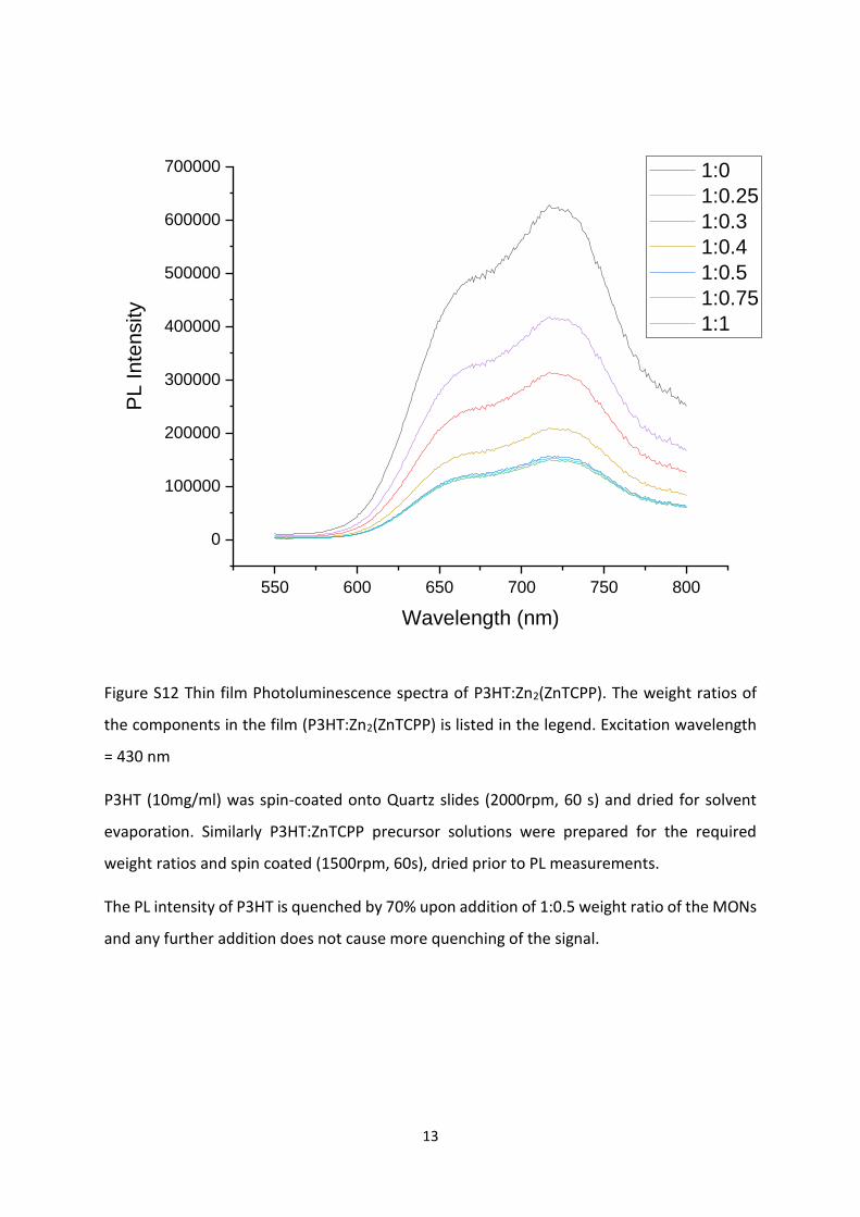
Figure S12 Thin film Photoluminescence spectra of P3HT:Zn2(ZnTCPP). The weight ratios of
the components in the film (P3HT:Zn2(ZnTCPP) is listed in the legend. Excitation wavelength
= 430 nm
P3HT (10mg/ml) was spin-coated onto Quartz slides (2000rpm, 60 s) and dried for solvent
evaporation. Similarly P3HT:ZnTCPP precursor solutions were prepared for the required
weight ratios and spin coated (1500rpm, 60s), dried prior to PL measurements.
The PL intensity of P3HT is quenched by 70% upon addition of 1:0.5 weight ratio of the MONs
and any further addition does not cause more quenching of the signal.
550 600 650 700 750 800
0
100000
200000
300000
400000
500000
600000
700000
PL Inte
nsity
Wavelength (nm)
1:0
1:0.25
1:0.3
1:0.4
1:0.5
1:0.75
1:1

14
6. Casting of films
6.1 Optimization of spin parameters
Figure S13 Calibration curve of thickness of the spin-coated films as a function of spin speed
(t=60 seconds). Concentration of spin coat precursor solutions are: P3HT- 10 mg/ml; P3HT-
Zn2(ZnTCPP)- 10 mg/ml (1:0.5); P3HT:PCBM- 10 mg/ml (1:1); P3HT-Zn2(ZnTCPP)-PCBM-
10mg/ml (1:0.5:1)
0 500 1000 1500 2000 2500 3000
20
40
60
80
100
120
140
160
180
200
0 500 1000 1500 2000 2500 3000
20
40
60
80
100
120
140
160
180
200
0 500 1000 1500 2000 2500 3000
20
40
60
80
100
120
140
160
180
200
0 500 1000 1500 2000 2500 3000
20
40
60
80
100
120
140
160
180
200 P3HT-PCBM
Film
thic
kness (
nm
)
Spin speed (rpm)
P3HT-Zn2(ZnTCPP)-PCBM P3HT P3HT-Zn2(ZnTCPP)
15
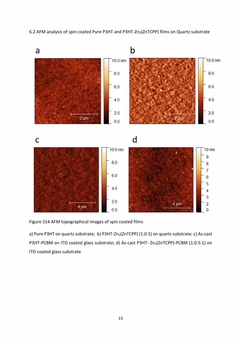
6.2 AFM analysis of spin coated Pure P3HT and P3HT-Zn2(ZnTCPP) films on Quartz substrate
Figure S14 AFM topographical images of spin coated films
a) Pure P3HT on quartz substrate; b) P3HT-Zn2(ZnTCPP) (1:0.5) on quartz substrate; c) As-cast
P3HT-PCBM on ITO coated glass substrate; d) As-cast P3HT- Zn2(ZnTCPP)-PCBM (1:0.5:1) on
ITO coated glass substrate

16
7. Fabrication of devices
7.1 Preparation of substrates
Pre-patterned ITO Glass substrates (20 mm x 15 mm) of 20 ohm/square resistance (Ossila)
were cleaned via hellmenex (1-3vol%) in boiling DI water (10-minute sonication), followed by
further washing in boiling DI water (10-minute sonication) and finally 5-10 minutes sonication
in isopropyl alcohol. The substrates were dried with a nitrogen gun and placed in a UV-Ozone
cleaner for 10 minutes to ensure removal of any surface particulates.
7.2 Deposition of PEDOT:PSS
PEDOT:PSS solution (Al4083, Ossila) was brought to room temperature, filtered through a
0.45 µm PVDF filter into an amber vial and dynamically spin-coated (45 µL) onto room-temp
substrates at 6000 rpm, to achieve a film ~25 nm. The PEDOT:PSS coated substrates were
placed on a hotplate at 110 °C for 15 minutes. This was followed by further annealing in the
glovebox at 110 °C for 15 minutes to remove any surface moisture. After 15 minutes annealing
in the glovebox, the ITO/PEDOT samples were cooled to room temperature before active
layer deposition.
7.3 Active layer deposition
P3HT (Sigma Aldrich) and PCBM (99% purity, supplied by Ossila) were used as received. P3HT
(10mg/mL) was dissolved in chlorobenzene (CB) solvent. After heating at 60 °C for 10 minutes
followed by cooling towards room temperature, the solution was filtered through a 0.45 um
PTFE filter. The P3HT solution in chlorobenzene was then mixed with 5mg ZnTCPP MONs
(1:0.5 wt/wt ratio of P3HT:ZnTCPP)) and stirred at 60 °C for an hour. Then 10 mg of PCBM was
added and the final P3HT:ZnTCPP:PCBM (1:0.5:1 wt/wt ratio) was heated at 70°C for an hour
and cooled to room temperature prior to spin coating. The solutions were then spin-cast onto
ITO/PEDOT at 1000 rpm under a nitrogen atmosphere in a glove box, forming films of ∼150
nm as determined by dektak. For control devices, 1:1(wt/wt) (P3HT:PCBM) were spin cast at
2000 rpm in the same method as above to give films of ~150nm. Solvent-vapour annealing of
the films was carried out by placing the coated substrates in a sealed metal container
containing 20uL of solvent chlorobenzene) for 5 minutes.
7.4 Top contact deposition and encapsulation

17
The ITO/PEDOT:PSS/Active layer substrates were placed under a vacuum of <2E-6 mBar
before thermally evaporating BCP (5nm) and Silver (100nm) layers using a shadow mask. The
devices were encapsulated using an epoxy resin (Ossila, E131).
7.5 Device testing
Device performance was determined under ambient conditions by measuring J–V curves
using a Newport 92251A‐1000 solar simulator, with devices illuminated through a 0.0256 cm2
aperture mask. Before each set of measurements, the intensity was calibrated to 100 mW
cm−2 using an NREL certified silicon reference cell. The applied bias was swept from 0.0 to
+1.2 V and back again at a scan speed of 0.4 V s−1 using a Keithley 237 source measure unit.
External quantum efficiencies were measured using a white light source that was
monochromated using a Spectral Products DK240 monochromator that was then imaged on
the PSC active area. The intensity of the monochromated light was determined using a
calibrated silicon photodiode having a known spectral response. The external quantum
efficiency was measured in the spectral range 400-700 nm using an Xtralien X100 (Ossila)
source measure unit to determine the PSC photocurrent.
Laser beam induced current (LBIC) mapping was performed on the ternary blend devices. The
system comprised a mechanically chopped laser that was passed through a spatial filter
before being focused to a spot size of ~1 μm onto the sample via a 50x Mitutoyo infinity‐
corrected long working distance objective. The sample was mounted on a computer
controlled XY‐stage, and moved in a sawtooth pattern in steps of 1 μm. A blue 3mW, 405 nm
diode laser (power density of 27 W/cm2) used to generate photocurrent. Photocurrent was
measured using a Stanford Research Systems SR830 lock‐in amplifier referenced to the
chopped laser.

18
Figure S15a Current-density-voltage curves of P3HT-Zn2(ZnTCPP)-PCBM devices.
0.0 0.2 0.4 0.6 0.8
-10
-5
0
5
10
15
20C
urr
ent density (
mA
/cm
2)
Applied bias (V)
As cast
Thermal annealed
Solvent vapour annealed
Solvent+Thermal annealed

19
Figure S15b- Current-density-voltage curves of P3HT-PCBM devices

20
Table S1 Device performance metrics corresponding to the different blend ratios and
processing conditions used in this work for optimization. All the results shown here are
averaged values of data obtained from a set of 35 devices each.
Active layer (P3HT:Zn2ZnTCPP:
PCBM)
Jsc
(mA/cm2)
Voc
(V)
FF (%)
PCE (%)
PCE (%)
Champion
device
Varying composition of active layer
a 1:0:1 5.25±0.31 0.64±0.06 49.21±2.50 1.94±0.14 2.02
b 1:0.25:1 6.34±0.21 0.64±0.02 50.26±1.40 2.27±0.23 2.50
c 1:0.5:1 8.42±0.20 0.69±0.05 59.17±1.27 3.24±0.35 3.60
d 1:1:1 7.23±0.12 0.66±0.07 35.87±3.20 1.87±0.02 1.90
Thermal annealing
e 1:0:1 6.11±0.40 0.66±0.05 51.64±2.74 2.04±0.04 2.09
f 1:0.5:1 8.72±0.32 0.70±0.04 60.12±0.85 3.63±0.15 3.96
Solvent vapour annealed
g 1:0:1 6.50±0.23 0.65±0.03 53.21±1.70 2.25±0.23 2.46
h 1:0.5:1 9.51±0.31 0.70±0.05 62.70±0.72 4.06±0.10 4.21
Solvent + thermal annealed
i 1:0:1 7.09±0.15 0.66±0.02 57.44±2.20 2.67±0.01 2.67
j 1:0.5:1 10.54±0.2 0.70±0.03 63.12±0.15 4.65±0.30 5.20
7.6 Analysis of device data reported in literature.
Scifinder search yielded 65 literature results containing the search keywords “P3HT”, “PCBM” and
“BCP”. Out of these reports, devices with plasmon modified hybrid systems, with <1% power
conversion efficiencies or which were only reported as a patent were excluded. The remaining 38
device results from 18 papers are shown in figure S2 and used in for the statistical analysis given in
Figure 3.

21
Table S2. The configuration and performance parameters of the devices used for statistical
analysis in Figure 3
Configuration Jsc Voc FF PCE
P3HT-PC71BM/BCP/Al2 14.21 0.58 57.8 4.79
P3HT-PCBM/BCP/Ag/Wox3 P3HT-PCBM/Yb/BCP/Ag/Wox3
6.33 0.54 60.2 2.07
6.68 0.55 65.4 2.42
P3HT-PCBM/BCP/Al4 11.74 0.59 62.29 4.31
P3HT-PCBM/BCP/Al5
9.76 0.63 60 3.72
9.55 0.65 57 3.52
9.38 0.64 56 3.36
10.02 0.64 41 2.61
9.41 0.63 62.73 3.74
10.22 0.64 63 4.11
P3HT-PCBM-PMMA/BCP/Al6 5.41 0.61 52.6 1.65
4.18 0.61 45.5 1.16
P3HT-PCBM/BCP/Al6 4.35 0.59 52.2 1.34
4.51 0.59 51.1 1.36
P3HT-PCBM/BCP/Al7 10 0.64 60 3
P3HT-PCBM/BCP/Al8 6.28 0.61 38 2.66
P3HT-PCBM/BCP/LiF/Al9 12.31 0.645 44.5 3.54
P3HT-PCBM/MoO3/ ZnPc/C60/BCP/LiF-Al10
4.76 0.457 56.6 1.21
4.23 0.57 58.3 1.42
5.68 0.48 56.0 1.53
P3HT-PCBM/Ca-Al/Subpc/C60/BCP/Ag11 8 0.55 60 3.00
P3HT-PCBM-BCP/LIF-Al12 8.88 0.59 39.1 2.05
P3HT-PCBM/BCP/Al13 9.64 0.63 61.2 3.72
P3HT-PCBM/BCP/LiF/Al14 10.83 0.56 65.2 3.74
P3HT-PCBM/BCP/Ag15 8 0.6 60 3.5
P3HT-PCBM/BCP/Al16 11.06 0.59 40 2.64
P3HT-PCBM/BCP-LiQ16 11.30 0.66 58 4.29
ZnO/BCP/P3HT-PCBM/MoO3/Al17 9.23 0.61 62 3.49
8.53 0.50 35 1.50
8.85 0.58 60 3.08
8.68 0.59 55 2.82
CsCl/BCP/P3HT-PCBM/MoO3/Al18 9.43 0.59 54.1 3.00
9.49 0.60 58.6 3.31
BCP/P3HT-PCBM/MoO3/Al18 9.24 0.53 50.1 2.50
P3HT-PCBM/BCP/Al19 4.51 0.65 42 1.24
6.29 0.61 52 1.99
P3HT-PCBM/BCP-LiF/Al20 4.58 0.66 41 1.25
6.12 0.61 49 1.85

22
Figure S16. J-V curve of P3HT/TCPP-ligand/PCBM ternary device.
0.0 0.2 0.4 0.6 0.8 1.0 1.2
-20
0
20
Curr
ent density (
mA
/cm
2)
Bias (V)
P3HT-TCPP-PCBM

23
8. Transient absorption and Kinetics
We recorded transient absorption (TA) spectra for P3HT-PCBM and P3HT/Zn2(ZnTCPP)/PCBM
samples using broadband probe pulses spanning both NIR (850nm-1300nm) and UV-visible
(350nm-750nm) regions (see methods). During the UV-visible measurement, both samples
were observed to degrade slightly over the course of several sweeps. The data presented in
this section is taken from the first sweep only. Note that Figure 5c in the main text displays
data averaged over 5 sweeps, hence the signal magnitude is slightly weaker.
The following transient absorption features were observed and assigned by reference to
previous reports:21–24
1. Ground state bleach (GSB) at 470-530nm
2. Polaron pair photoinduced absorption (PIA) at 600-700nm (charge-pairs in P3HT or
charge transfer states at theP3HT/PCBM interface)
3. Polaron photoinduced absorption (PIA) at 900-1000nm (free charges in P3HT
overlapped with the singlet PIA at times < 10ps)
4. Singlet exciton photoinduced absorption (PIA) 1000-1400nm (photogenerated singlet
exciton in P3HT).
No obvious new TA features were observed when Zn2(ZnTCPP) was added to the blend.
However, the TA signal for the sample with Zn2(ZnTCPP) added is roughly twice that of the
sample without (Figure S17a-b). This gives evidence of enhanced light absorption in the blend
with the nanosheets, corresponding to higher current density in the solar cell performance.
Of all the TA features, the singlet PIA feature around 1300nm increased less than the other
features when Zn2(ZnTCPP) is added. Evaluation of kinetics of the P3HT-PCBM and P3HT-
Zn2(ZnTCPP)-PCBM blends show no real change in the excited state dynamics upon addition
of Zn2(ZnTCPP), at least on timescales ranging from 1ps to 1ns (Figure S18a). Addition of
Zn2(ZnTCPP) seems to cause a large relative increase (more than twofold) in the population
of charges in P3HT (Figure S18b).
24
Figure S17. Transient absorption spectra of a. P3HT-PCBM film and b. P3HT-ZnTCPP-PCBM
film.
Figure S18a: Comparison of kinetics of the blends (normalized). No significant change in the
excited state dynamics is observed upon addition of Zn2(ZnTCPP), at least on timescales
ranging from 1ps to several ns.

25
Figure S18b: Dynamics of excitons and charges in P3HT-PCBM blends with and without
addition of Zn2(ZnTCPP). Here, the signal from PIA associated with charges (red and blue) has
been normalised to the maximum (i.e. initial value) of the PIA associated with singlet excitons
(black). It appears that the film with Zn2(ZnTCPP) has a much higher population of charge pairs
(red) as a proportion of the photoexcited singlet exciton population. However, this doesn’t
seem to be replicated for the free-charge population (blue).
Methods for TA studies: For transient absorption (TA) measurements, a Ti:sapphire
regenerative amplifier (Spitfire ACE PA-40, Spectra-Physics) providing 800nm pulses (40fs
FWHM, 10kHz, 1.2mJ) was used to generate both the pump and probe beams. Narrowband
pump pulses at 500nm were generated in an optical parameteric amplifier (TOPAS Prime,
Light Conversion). Probe pulses spanning the ranges 350-750nm and 850-1300nm were
generated by focussing a portion of the 800nm beam through a continuously translating
calcium fluoride or sapphire crystal, respectively. Pump-probe delay was controlled using a
motorized linear stage. Detection was carried out using a commercial instrument (Helios,
Ultrafast Systems) equipped with CMOS and InGaAs detectors for the UV-visible and NIR
probe regions respectively. The pump and probe polarizations were set to magic angle. The
pump beam spot size was measured at the sample position using a CCD beam profiler
(Thorlabs). The pump pulse energy was approximately 130µJcm-2. Data processing
(background correction, correlated noise removal and chirp correction) were performed using
a custom-made MATLAB programme.
9. SCLC devices for charge carrier mobility measurement
The investigation of space-charge limited electron-only or hole-only devices for extraction of
mobility values is a well-known and reliable method. Space-charge limited currents were
tested in hole only devices with the configuration ITO:PEDOT/PSS:active layer:MoO3:Ag and
a well-established protocol from literature was used for data fitting and analysis25. The hole
mobility was determined by fitting the dark current to the model of a single carrier SCLC
current with field dependent mobility based on Mott-Gurney law (Figure S19a-S22b, ESI).
Electron only devices were fabricated with the configuration ITO:ZnO:Active layer:BCP:Ag to
extract the electron mobility.

26
Table S3 Hole mobility and electron mobility extracted from SCLC holes only and electrons only
devices for different thicknesses of active layer; Number of devices tested for each thickness=3.
Device
configuration
Active layer
(nm)
µh
(cm2/Vs)
µe
(cm2/Vs)
P3HT-PCBM 100 (6.06±0.50)x10-4 (3.77±0.71)x10-3
150 (1.13±0.17)x10-4 (1.35±0.07)x10-3
P3HT-Zn2(ZnTCPP)-PCBM 100 (3.20±0.48)x10-3 (2.14±0.46)x10-3
150 (2.12±0.34)x10-3 (2.13±0.14)x10-3
Figure S19(a)-S22(b): The J–V characteristics of electron and hole only devices in different
structures and active layer thickness. The bias is corrected for built-in voltage , arising from
difference in the work function of the contacts, and the voltage drop due to substrate series
resistance.

27

28

29

30
31
The devices were prepared following the same procedure described in the experimental
section for photovoltaic devices, except that of the metal electrode. The mobilities were
determined by fitting the dark current to the model of a single carrier SCLC current with field
dependent mobility25, which is described as
J= [(9 ɛrɛ0 µ0V2)/8L3 ] exp(𝛽√𝑉/𝐿)
Where, J is the current, µ0is the zero-field mobility, ɛ0 is the permittivity of free space, ɛr is the
relative permittivity of the material, V is the effective voltage, and L is the thickness of the
active layer.
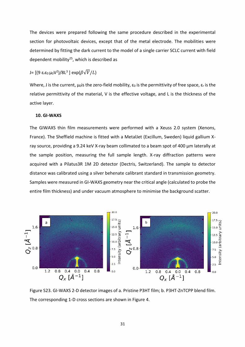
10. GI-WAXS
The GIWAXS thin film measurements were performed with a Xeuss 2.0 system (Xenons,
France). The Sheffield machine is fitted with a MetalJet (Excillum, Sweden) liquid gallium X-
ray source, providing a 9.24 keV X-ray beam collimated to a beam spot of 400 µm laterally at
the sample position, measuring the full sample length. X-ray diffraction patterns were
acquired with a Pilatus3R 1M 2D detector (Dectris, Switzerland). The sample to detector
distance was calibrated using a silver behenate calibrant standard in transmission geometry.
Samples were measured in GI-WAXS geometry near the critical angle (calculated to probe the
entire film thickness) and under vacuum atmosphere to minimise the background scatter.
Figure S23. GI-WAXS 2-D detector images of a. Pristine P3HT film; b. P3HT-ZnTCPP blend film.
The corresponding 1-D cross sections are shown in Figure 4.
a b
32
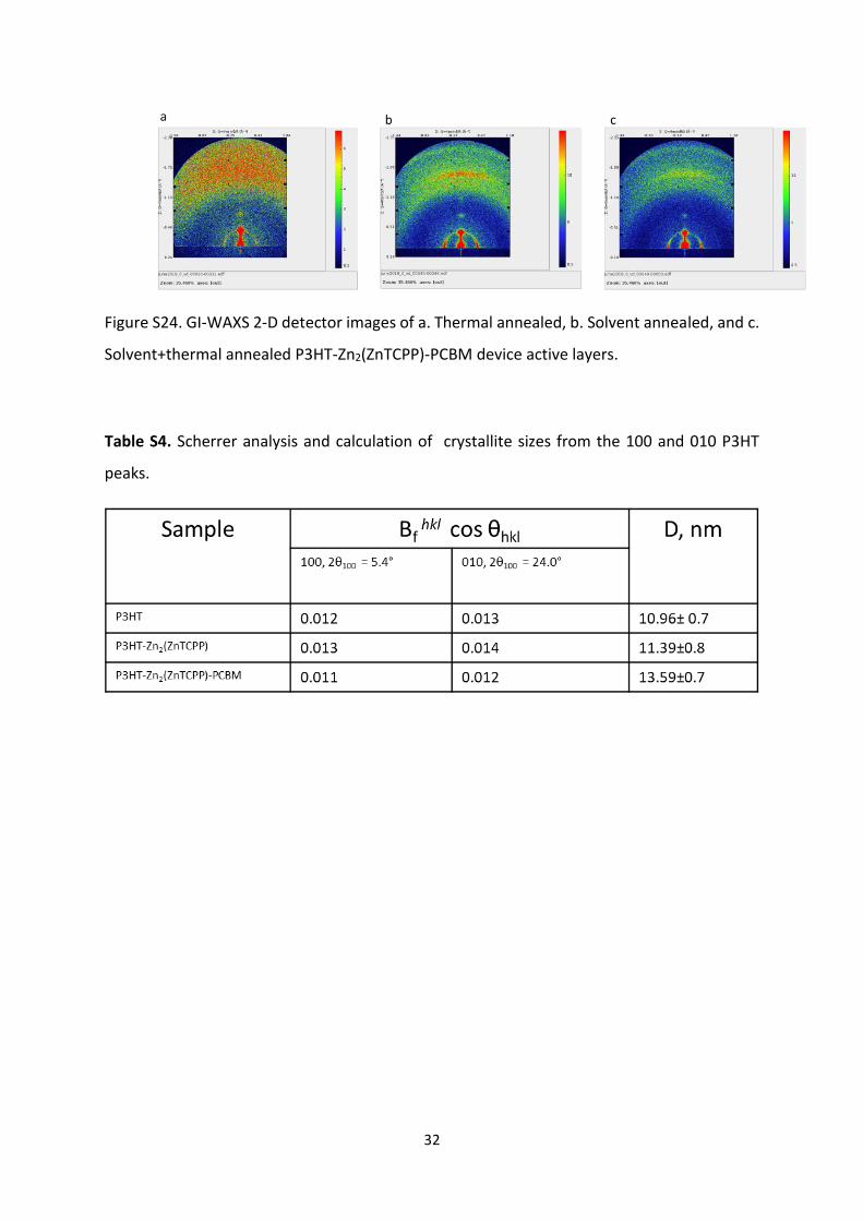
Figure S24. GI-WAXS 2-D detector images of a. Thermal annealed, b. Solvent annealed, and c.
Solvent+thermal annealed P3HT-Zn2(ZnTCPP)-PCBM device active layers.
Table S4. Scherrer analysis and calculation of crystallite sizes from the 100 and 010 P3HT
peaks.

33
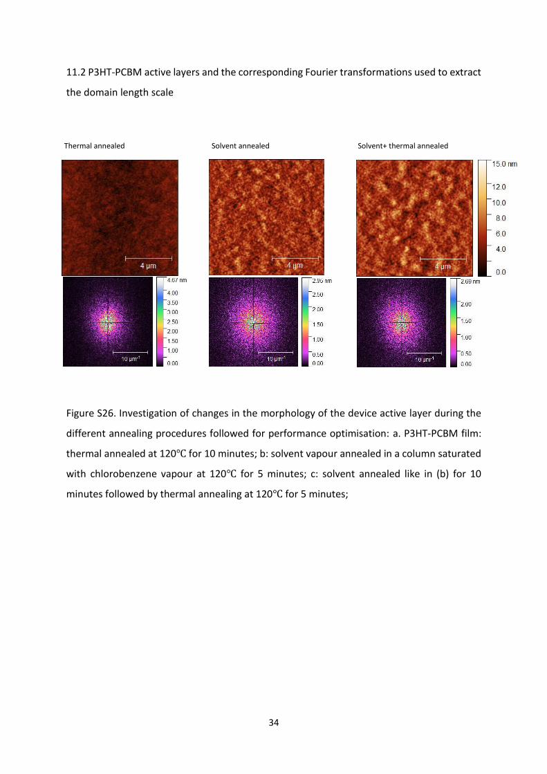
11. AFM – Morphological investigation of the device active layers
11.1 P3HT-Zn2(ZnTCPP)-PCBM active layers and the corresponding Fourier transformations
used to extract the domain length scale
Figure S25. Investigation of changes in the morphology of the device active layer during the
different annealing procedures followed for performance optimisation: a. P3HT-Zn2(ZnTCPP)-
PCBM film: thermal annealed at 120℃ for 10 minutes; b: solvent vapour annealed in a column
saturated with chlorobenzene vapour at 120℃ for 5 minutes; c: solvent annealed like in (b)
for 10 minutes followed by thermal annealing at 120℃ for 5 minutes;
Thermal annealed Solvent annealed Solvent+ thermal annealed
34
11.2 P3HT-PCBM active layers and the corresponding Fourier transformations used to extract
the domain length scale
Figure S26. Investigation of changes in the morphology of the device active layer during the
different annealing procedures followed for performance optimisation: a. P3HT-PCBM film:
thermal annealed at 120℃ for 10 minutes; b: solvent vapour annealed in a column saturated
with chlorobenzene vapour at 120℃ for 5 minutes; c: solvent annealed like in (b) for 10
minutes followed by thermal annealing at 120℃ for 5 minutes;
Thermal annealed Solvent annealed Solvent+ thermal annealed

35
12. Spectroscopic ellipsometry
For fitting of the data, J. A. Woollam WVASE32 Software was used. During the fitting,
reasonable boundaries were set for model parameters to restrict them to physically
meaningful values. Fitting in the range of 700−900 nm was performed first using a Cauchy
model and the thickness value determined by a step-profiler as the initial guess to obtain a
good estimate of film thickness. Then, a B-spline model incorporating a Kramers Kronig model
was used to fit the n and k were fitted in the desired wavelength range with the thickness
fixed. Finally, both thickness and optical functions were allowed to vary in the last fitting run
to verify that a reasonable solution has been obtained.
400 500 600 700 800
1.2
1.4
1.6
1.8
2.0
2.2
2.4
400 500 600 700 800
1.2
1.4
1.6
1.8
2.0
2.2
2.4
Wavelength (nm)
P3HT-Zn2(ZnTCPP)
-0.4
0.0
0.4
0.8
1.2
1.6
2.0
n
P3HT
-0.4
0.0
0.4
0.8
1.2
1.6
2.0
kk
k
n
n
Figure S27. The extinction coefficient spectra and wavelength dependant refractive index
plots of P3HT and P3HT-Zn2(ZnTCPP) extracted using spectroscopic ellipsometry;
Figure S28. The optical properties of the device active layer as a function of annealing
conditions extracted using spectroscopic ellipsometry
400 500 600 700 800 900
1.2
1.4
1.6
1.8
2.0
2.2
2.4
n
Wavelength (nm)
0.00
0.25
0.50
0.75
1.00
k
nk

36
13. References
1 M. Zhao, Y. Wang, Q. Ma, Y. Huang, X. Zhang, J. Ping, Z. Zhang, Q. Lu, Y. Yu, H. Xu, Y. Zhao and H. Zhang, Adv. Mater., 2015, 27, 7372–7378.
2 A. Singh, A. Dey and P. K. Iyer, Org. Electron., 2017, 51, 428–434.
3 I. S. Oh, C. H. Ji and S. Y. Oh, 2016, 12, 156–162.
4 D. Wang, W. Zeng, S. Chen, X. Su, J. Wang and H. Zhang, Semicond. Sci. Technol., , DOI:10.1088/0268-1242/30/8/085017.
5 C. A. Tseng, H. C. Han, C. W. Chong, C. C. Chang, C. F. Lin, S. B. Wang, W. H. Tseng, C. I. Wu, J. H. Lee, S. J. Chang, K. H. Chen and L. C. Chen, ACS Appl. Mater. Interfaces, 2015, 7, 6683–6689.
6 D. Qin, W. Wang, M. Wang, S. Jin and J. Zhang, Semicond. Sci. Technol., , DOI:10.1088/0268-1242/29/12/125011.
7 A. Colsmann, J. Junge, C. Kayser, T. Wellinger and U. Lemmer, Org. Optoelectron. Photonics II, 2006, 6192, 619220.
8 Z. Feng, Y. Hou and D. Lei, Renew. Energy, 2010, 35, 1175–1178.
9 Z. Yi Wang, S. H. Lee, D. H. Kim, J. H. Kim and J. G. Park, Sol. Energy Mater. Sol. Cells, 2010, 94, 1591–1596.
10 D. Lee, W. Ki Bae, I. Park, D. Y. Yoon, S. Lee and C. Lee, Sol. Energy Mater. Sol. Cells, 2011, 95, 365–368.
11 R. J.K. Baral, M. Izquierdo, Packirisamy and V.-V. Truong, Eur. Phys. J. Appl. Phys., 2011, 55, 30202.
12 D. Qin, W. Quan, J. Liu, G. Li, L. Chen, J. Zhang and D. Yan, Phys. Status Solidi A, 2012, 1156, 1150–1156.
13 W. H. Tseng, M. H. Chen, C. C. Chang, W. H. Lin, L. C. Chen, K. H. Chen and C. I. Wu, Thin Solid Films, 2012, 520, 5413–5416.
14 G. Cheng, W. Y. Tong, K. H. Low and C. M. Che, Sol. Energy Mater. Sol. Cells, 2012, 103, 164–170.
15 G. H. Jung and J. L. Lee, J. Mater. Chem. A, 2013, 1, 3034–3039.
16 K. Xu, D. H. Kim, S. H. Lee and T. W. Kim, Thin Solid Films, 2013, 547, 116–119.
17 J. Li, X. Huang, J. Yuan, K. Lu, W. Yue and W. Ma, Org. Electron. physics, Mater. Appl., 2013, 14, 2164–2171.
18 T. Xiao, F. Fungura, M. Cai, J. W. Anderegg, J. Shinar and R. Shinar, Org. Electron. physics, Mater. Appl., 2013, 14, 2555–2563.
19 G. Williams and H. Aziz, Org. Electron. physics, Mater. Appl., 2014, 15, 47–56.
20 G. Williams and H. Aziz, Org. Electron. physics, Mater. Appl., 2014, 15, 47–56.
21 J. Piris, T. E. Dykstra, A. A. Bakulin, P. H. M. Van Loosdrecht, W. Knulst, M. T. Trinh, J.

37
M. Schins and L. D. A. Siebbeles, J. Phys. Chem. C, 2009, 113, 14500–14506.
22 I. W. Hwang, D. Moses and A. J. Heeger, J. Phys. Chem. C, 2008, 112, 4350–4354.
23 G. Grancini, D. Polli, D. Fazzi, J. Cabanillas-Gonzalez, G. Cerullo and G. Lanzani, J. Phys. Chem. Lett., 2011, 2, 1099–1105.
24 Y. Tamai, Y. Matsuura, H. Ohkita, H. Benten and S. Ito, J. Phys. Chem. Lett., 2014, 5, 399–403.
25 J. C. Blakesley, F. A. Castro, W. Kylberg, G. F. A. Dibb, C. Arantes, R. Valaski, M. Cremona, J. Soo and J. Kim, Org. Electron., 2014, 15, 1263–1272.