METAL INSULATOR MULTI-LAYER SURFACE PLASMON …tc335tx2847/final... · METAL INSULATOR MULTI-LAYER...
91
METAL INSULATOR MULTI-LAYER SURFACE PLASMON DEVICES A DISSERTATION SUBMITTED TO THE DEPARTMENT OF MATERIALS SCIENCE AND ENGINEERING AND THE COMMITTEE ON GRADUATE STUDIES OF STANFORD UNIVERSITY IN PARTIAL FULFILLMENT OF THE REQUIREMENTS FOR THE DEGREE OF DOCTOR OF PHILOSOPHY Anu Chandran August 2014
Transcript of METAL INSULATOR MULTI-LAYER SURFACE PLASMON …tc335tx2847/final... · METAL INSULATOR MULTI-LAYER...
METAL INSULATOR MULTI-LAYER SURFACE PLASMON
DEVICES
A DISSERTATION
SUBMITTED TO THE DEPARTMENT OF MATERIALS
SCIENCE AND ENGINEERING
AND THE COMMITTEE ON GRADUATE STUDIES
OF STANFORD UNIVERSITY
IN PARTIAL FULFILLMENT OF THE REQUIREMENTS
FOR THE DEGREE OF
DOCTOR OF PHILOSOPHY
Anu Chandran
August 2014

http://creativecommons.org/licenses/by-nc/3.0/us/
This dissertation is online at: http://purl.stanford.edu/tc335tx2847
© 2014 by Anu Chandran. All Rights Reserved.
Re-distributed by Stanford University under license with the author.
This work is licensed under a Creative Commons Attribution-Noncommercial 3.0 United States License.
ii
I certify that I have read this dissertation and that, in my opinion, it is fully adequatein scope and quality as a dissertation for the degree of Doctor of Philosophy.
Mark Brongersma, Primary Adviser
I certify that I have read this dissertation and that, in my opinion, it is fully adequatein scope and quality as a dissertation for the degree of Doctor of Philosophy.
Jennifer Dionne
I certify that I have read this dissertation and that, in my opinion, it is fully adequatein scope and quality as a dissertation for the degree of Doctor of Philosophy.
Shanhui Fan
Approved for the Stanford University Committee on Graduate Studies.
Patricia J. Gumport, Vice Provost for Graduate Education
This signature page was generated electronically upon submission of this dissertation in electronic format. An original signed hard copy of the signature page is on file inUniversity Archives.
iii

Preface
Surface plasmon based devices have attracted significant of attention over the last
decade with exciting applications like negative refraction, optical cloaking, perfect
lenses, and meta-surfaces. They have also enabled highly efficient and compact
electro-optical devices bridging the gap between optical (micron) and the electronics
(nano) scale devices. At the heart of many of these devices and applications are
multi-layer metal insulator structures, where the interaction of surface plasmons at
various interfaces unlock these surprising properties. This thesis focuses on the scat-
tering and transmission properties of plasmon modes in metal insulator multilayer
structures.
In the first part of the thesis, we will describe a theoretical model for standing wave
resonances in Metal-Insulator-Metal surface plasmon cavities. These calculations,
which are in excellent agreement with full field finite difference simulations, aid in
furthering our understanding of plasmon phase pickup on reflection from the cavity
terminations. This phase pickup is associated with the near-field energy storage at
those terminations, and the imaginary part of the reflection coefficient is shown to be
approximately proportional to the stored energy.
We then focus on a different, yet related geometry for a surface plasmon antenna, a
metal stripe wave guide above a metallic ground plane. Staggered confocal microscopy
is used to study the scattering properties of the stripe antenna. CdSe/ZnS quantum
dots are sandwiched between the stripe and ground plane. Dual purposing of the
stripes as electrical lead and an optical element is illustrated through low temperature
quantum confined stark effect measurements. Finite difference calculations of the
surface plasmon transmission spectra through the truncated stripe waveguide cavity
iv

is shown to be well modeled by a two-path-two-mode coupled cavity model.
v

Acknowledgements
I would like to thank Mark, my thesis advisor, for his support and guidance. He was
very patient with me, giving enough latitude to pursue different lines of investigations.
He was always accommodating, even when some of those investigations bore no fruit.
But above all I would like to thank him for his kindness and sensitivity during my
late wife’s unsuccessful battle with cancer.
There are quite a few people in Stanford that I would like to thank, and it is only
at the interest of brevity that I don’t mention all by name. Prof. Shanhui Fan, for
introducing me to fundamentals of optics and waveguide theory, Prof. Nick Melosh
and his students for extreme generosity with chemicals and lab equipments during
fabrication runs and Dr James Conway for always being there for help with e-beam
lithography.
I consider my interaction with Rashid Zia a highlight of my Stanford experience.
Rashid, introduced a much needed dose of heavy skepticism into me, which ultimately
made me, in my opinion, a better scientist. I would like to thank Edward Barnard
for all the fun times exploring slashdot, hacker news, and experiments with arduino.
Ed has the habit of always showing up just at the right place at the right time to
help. I should also definitely mention David Barsic for showing me the delicate art
of nano-optics with toothpicks and Jon Schuller, random-T-shirt-baggy-jeans-rap-
star, for helping me realize that science does not always have to be straight laced.
I would like to thank Patrick Landreman, and Xinpeng Huang for their help with
administrative issues while I was working remotely from Houston. I would like to
thank all the group members (past and present) for an extremely enjoyable experience:
Alex, Alok, (F)anu, Justin, Linyou, Mark Selker, Ragip, Rohan, Ken, Mike, Pengyou
vi

and Young-Chul.
I would also like to express my gratitude to the whole Bechtel International center
staff, who work very hard to help foreign students jump through the visa hurdles.
I would like to thank my parents, for their love and support without which I would
not have reached this far. I would also thank my dear wife Ammu for her support
and my daughter, little Tenaya, just for being there in my life.
vii
Contents
Preface iv
Acknowledgements vi
1 Sub-wavelength optical cavities 1
1.1 Metal-Dielectric-Metal Plasmon Devices . . . . . . . . . . . . . . . . 5
1.1.1 Surface plasmon dispersion in MDM structures . . . . . . . . 5
1.1.2 Emitter plasmon interaction in metal-dielectric structures . . . 7
1.2 Outline of this thesis . . . . . . . . . . . . . . . . . . . . . . . . . . . 9
2 MIM plasmon cavities 11
2.1 SPP Modes of MDM structures . . . . . . . . . . . . . . . . . . . . . 12
2.1.1 Transmission into the cavity . . . . . . . . . . . . . . . . . . . 13
2.1.2 Calculation of the SPP reflection coefficient . . . . . . . . . . 15
2.1.3 Cavity Properties . . . . . . . . . . . . . . . . . . . . . . . . . 15
2.1.4 Origin of the reflection phase . . . . . . . . . . . . . . . . . . 16
2.1.5 Model Validation . . . . . . . . . . . . . . . . . . . . . . . . . 19
2.2 Numerical Results . . . . . . . . . . . . . . . . . . . . . . . . . . . . . 20
2.3 Conclusion . . . . . . . . . . . . . . . . . . . . . . . . . . . . . . . . . 26
3 Surface Plasmon Patch Antenna 27
3.1 Experiment . . . . . . . . . . . . . . . . . . . . . . . . . . . . . . . . 29
3.2 Scattering under normal illumination . . . . . . . . . . . . . . . . . . 32
3.3 Plasmon interference in patch antenna structures . . . . . . . . . . . 36
viii

3.4 Coupled cavity model for plasmon scattering . . . . . . . . . . . . . . 41
4 Electrical modulation 46
4.1 Introduction . . . . . . . . . . . . . . . . . . . . . . . . . . . . . . . . 46
4.2 Sample fabrication and experiment details . . . . . . . . . . . . . . . 47
4.3 Quantum Confined Stark Effect . . . . . . . . . . . . . . . . . . . . . 50
5 Conclusion 53
A Plasmon reflection and excitation 56
A.1 Plasmon reflection at cavity termination . . . . . . . . . . . . . . . . 56
A.2 Cavity plasmon excitation from free space . . . . . . . . . . . . . . . 59
B Energy stored in the near-field 62
C Two mode cavity resonance 66
Bibliography 70
ix

List of Figures
1.1 Schematic and field profile for a single interface surface plasmon . . . 3
1.2 Methods of surface plasmon excitation . . . . . . . . . . . . . . . . . 4
1.3 Schematic of MDM structure, field profile and dispersion . . . . . . . 6
1.4 Some optical antenna examples . . . . . . . . . . . . . . . . . . . . . 8
2.1 Schematic of a finite length MDM cavity. Hy-field profile of the sym-
metric SPP mode is shown. . . . . . . . . . . . . . . . . . . . . . . . 13
2.2 |r| and φ (phase) for different values of εm as a function of scaled
dielectric thickness . . . . . . . . . . . . . . . . . . . . . . . . . . . . 21
2.3 Reflection amplitude |r| and φ (phase) for an Ag-Air-Ag MDM struc-
ture as a function of wavelength for different dins values. Solid lines:
Without loss. Dotted lines: With loss. . . . . . . . . . . . . . . . . . 22
2.4 rimλ for Ag-Air-Ag cavity for different dins . . . . . . . . . . . . . . 23
2.5 Transmission efficiency (Teff ) through a Ag-Air-Ag cavity for different
cavity lengths (L) as a function of wavelength. . . . . . . . . . . . . . 24
2.6 Cavity resonance length as a function of dielectric thickness for different
orders. Free space wavelength λ=900nm. (Ag-Air-Ag cavity with loss.) 25
2.7 Q-factor of the cavity vs cavity length for different dielectric thick-
nesses. Free space wavelength λ=800nm. Ag-Air-Ag cavity with loss 25
3.1 Schematic and SEM of patch antenna structure . . . . . . . . . . . . 29
3.2 Photograph of the Witec Alpha SNOM system . . . . . . . . . . . . 30
3.3 Schematic of the confocal scan configuration . . . . . . . . . . . . . . 31
3.4 Schematic of fabrication process . . . . . . . . . . . . . . . . . . . . 32
x

3.5 Confocal scan of patch antenna emission . . . . . . . . . . . . . . . . 33
3.6 Normalized confocal scan of patch antenna emission . . . . . . . . . . 34
3.7 Plasmon mode index and propagation length for patch antenna geometry 36
3.8 Schematic of plasmon scattering experiment and FDFD simulations . 37
3.9 Confocal scan of surface plasmon scattering . . . . . . . . . . . . . . 39
3.10 Normalized confocal scan of surface plasmon scattering . . . . . . . . 40
3.11 Coupled cavity model . . . . . . . . . . . . . . . . . . . . . . . . . . 42
3.12 Patch antenna transmission . . . . . . . . . . . . . . . . . . . . . . . 43
3.13 Coupled cavity interference . . . . . . . . . . . . . . . . . . . . . . . 45
4.1 Schematic of the stark shift measurement setup . . . . . . . . . . . . 48
4.2 QD temperature stability under ALD . . . . . . . . . . . . . . . . . 49
4.3 Photograph of the thermal stage mounted on the Witec SNOM . . . 49
4.4 Voltage dependent PL from quantum dots . . . . . . . . . . . . . . . 51
4.5 Wavelength shift as a function of electric field . . . . . . . . . . . . . 52
xi

Chapter 1
Sub-wavelength optical cavities
Deep sub wavelength cavities which allow mode confinement with high field concen-
tration are very attractive for small footprint active nanophotonic devices. The possi-
bility of concentrating light into a nanoscale volume has a profound effect on the effi-
ciency of linear and nonlinear optical processes, which often scale with the ratio of the
optical quality factor (Q) to the mode volume Vm. Traditional dielectric optical micro
cavities have very low losses and high quality factors, but suffer from mode volume lim-
itations. The optical modes in these structures cannot be confined to dimensions much
smaller than the wavelength in the dielectric. Metallic optical cavities, where energy
is stored in the Surface Plasmon Polariton (SPP) fields, can support modes confined
to volumes much smaller than the wavelength[1, 2, 3]. Despite their modest quality
factors (typically between 10-100), metallic cavities can have such small mode volumes
that they can outperform much higher Q dielectric microcavities (Q ∼ 106)[4, 5, 6].
As such, they have been proven useful for a variety of applications[1], including sin-
gle molecule sensing [7], spectroscopy [8, 9], optical trapping [10], surface enhanced
reactions[11, 12], spontaneous emission modification[13, 14, 15, 16], Surface Plasmon
Polariton (SPP) modulators[17, 18, 19, 20] and SPP sources [21, 22].
Surface plasmons are coherent collective electron oscillations that propagate along
a metal surface. They couple very strongly to electromagnetic waves, and as such
are better described as surface plasmon polaritons. For surface plasmons on a metal
surface with permittivity εm bounded by a dielectric material of permittivity εd we
1

CHAPTER 1. SUB-WAVELENGTH OPTICAL CAVITIES 2
can write the dispersion relationship as[23],
kx =ω
c
(εmεdεm + εd
)1/2
(1.1)
Here, kx is the wave vector along the metal-dielectric interface, ω the angular fre-
quency of the plasmon and c the velocity light in vacuum. At optical frequencies,
typical metals have Re[εm] < 0 and hence k > ωc. Maxwell’s equation constrains the
wave vectors such that (k2x + k2y + k2z)(1/2) = ω
c. So, the wave-vectors out of the plane
of propagation will be imaginary (with a small real component in the case of metals
with losses). This implies that the surface plasmon is confined to the metal dielec-
tric interface, propagates along the interface, but evanescently decays away from it.
A schematic of a surface plasmon field profile and dispersion relationship is shown
in Fig. (1.1). This is the most critical point of difference between surface plasmon
modes and optical modes in dielectric cavities. Metal-dielectric interface is capable of
supporting modes with higher momentum than what is allowed for electromagnetic
waves propagating in the dielectric material. Consequently, the usual limits of mode
confinement applicable to dielectric devices no longer apply for surface plasmon cav-
ities. The increase in field confinement is associated with increased resistive losses in
the metal, but with suitable low loss metal choice a wide variety of confinement and
propagation regimes unavailable to dielectric optical devices can be accessed in plas-
monic waveguides and cavities[24, 25] A useful simplified model for metal dispersion
in optical frequencies is the drude model in which the metal permittivity at frequency
ω is given by,
εm =
(1−
ω2p
ω2
)(1.2)
For low frequencies the εm is a large negative number and for ω = ωp/√
1 + εd, the
surface plasmon resonance frequency, we have, εm = −εd. From equation(1.1) we
now have kx → ∞. This of course is an idealization and in real metals with losses,
the wave vector only approaches a large finite value. The larger the propagation
wave vector faster the evanescent decay away from the interface, implying a strong

CHAPTER 1. SUB-WAVELENGTH OPTICAL CAVITIES 3
+ + + - - - - + + + + - - - - + H ¤
E
X
Z Dielectric
Metal
Surface Plasmon a) b)
c)
Figure 1.1: a) Schematic of surface plasmon fields on a metal dielectric interface.Plasmon propagates in the X-direction. This is a TM wave with H field directed outof the plane. b) The H field intensity near the interface. The field is strongly localizedto the surface, decaying evanescently to either side. c) The dispersion relation forsingle interface surface plasmon
confinement of energy to the interface. This dispersion related field confinement to
the interface is exploited in a wide variety of surface plasmon applications and devices.
Typically wave vector of a surface plasmon at a metal dielectric interface lies outside
the light line for the dielectric. This makes it difficult to efficiently couple free space
light to surface plasmon modes. There are many possible ways to provide extra
momentum to the incident radiation to facilitate coupling to the plasmon modes[29].
Fig. (1.2) shows some of the techniques traditionally employed in surface plasmon
excitation. A high index prism near a metal-dielectric surface, a grating with suitable
periodicity, a localized source of excitation like a probe tip with a broad spread
of available momentum states can all excite surface plasmons. In addition, other
methods like electrical excitation through hot electron tunneling, and coupling of

CHAPTER 1. SUB-WAVELENGTH OPTICAL CAVITIES 4
(g)
(d) (e) (f)
(a) (b) (c)
(h) (i)
(d)
Figure 1.2: Many methods for plasmon excitation. a) Kretchmann configurationb) Two layer Kretchmann configuration c) Otto configuration d) Excitation witha SNOM probe e) diffraction from a grating f) Scattering from surface features g)Excitation by a high energy electron beam h) Evanescent coupling from a tapered fiberi) Tunnel junction plasmon excitation. Figures taken from the following references.(a-f) [26], (g)[27], (h)[2] i)[28]
photoluminescence to surface plasmon modes are also employed in compact SPP
sources.

CHAPTER 1. SUB-WAVELENGTH OPTICAL CAVITIES 5
1.1 Metal-Dielectric-Metal Plasmon Devices
The geometry of the plasmon device can also determine the characteristics of the
surface plasmon excitations supported by it. When two metal-dielectric interfaces are
brought close to each other, the surface plasmons on the interfaces can interact and
split into degenerate modes with different wave vectors. This provides an additional
level of control over the plasmon resonance and confinement in devices. One very
simple and versatile class of such a surface plasmon device is the Metal-Dielectric-
Metal (MDM) surface plasmon geometry.
1.1.1 Surface plasmon dispersion in MDM structures
Surface plasmon modes in metal-dielectric-metal multilayer structures have been ex-
tensively studied in the past[3, 30]. They are most easily analyzed and understood
in a planar two-dimensional device geometry where the metal on either side of the
dielectric are assumed to be the same and infinitely thick. The proximity of the
two metal dielectric interfaces causes the splitting of the degenerate modes at those
interfaces. Due to the symmetry of the structure these modes have symmetric and
anti-symmetric field profile as shown in Fig. (1.3 a). A schematic of the resulting
dispersion relationship for the modes is shown in Fig. (1.3 b). As the dielectric layer
thickness ‘d’ is decreased the symmetric mode dispersion shifts to the right, giving the
mode lower wavelength and group velocity. As a consequence, a larger fraction of the
mode energy is stored in the metal, resulting in increased losses and consequently,
a lower propagation length. This high index mode is strongly confined with large
electric fields in the dielectric. Also, its high optical density of states makes it an
attractive mode to target for enhanced light matter interaction. The anti-symmetric
mode dispersion on the other hand, shifts towards the light line and has a larger
fraction of its energy guided through the dielectric. The complementary structure
to the MDM geometry is the DMD geometry, a thin metallic plate surrounded by di-
electric on either side. They can serve as nano-scale optical waveguides, guiding light
below the diffraction limit. A schematic of the structure and a plot of the plasmon
dispersion relation is shown in Fig. (1.3). For small metal thickness, the modes in

CHAPTER 1. SUB-WAVELENGTH OPTICAL CAVITIES 6
Symmetric Anti Symmetric
d
H-field profile Metal
Metal
ω
k =2π
λsp
Decreasing d
Single interface a) b)
Figure 1.3: a) Schematic of the MDM structure, and the magnetic field profile for thesymmetric and anti-symmetric modes. (b) A schematic of the dispersion relationshipfor the two modes. Single interface surface plasmon dispersion relationship is alsoincluded for highlighting the dispersion change with the dielectric thickness ‘d’
the structure split just like modes in the MDM geometry. Symmetric modes in the
plate geometry guide most of their energy through the dielectric and hence have very
long propagation length [31]. Metallic stripe waveguides and other similar structures
have found wide applicability in a variety of plasmon assisted optical devices [32, 33].
By truncating the multilayer metal dielectric structures to wavelength scale di-
mensions one can construct retardation based plasmon resonators[34, 35]. Of these,
finite-length metal dielectric metal cavities have attracted particular attention for
their ability to concentrate light to nanoscale dimensions[36] through the excitation
of wavelength-tunable cavity resonances[37]. The high field intensity in the dielec-
tric region make these structures well-suited for active plasmonic structures. MDM
plasmonic slits have also been shown to enhance optical absorption within materials
adjacent to the MDM end-face[38, 39]. The relative ease of fabricating the MDM
structures together with the possibility of using the metal layers as electrical contacts
also make this geometry well-suited for optoelectronic applications[17, 22, 40, 41].
Plasmonic cavities are most readily studied with full field simulations, which al-
though exact, do not lend themselves to a clear physical interpretation. Time or
frequency domain full field simulations correctly predict the resonance phenomena
in these cavities, but does not immediately make apparent the interaction of the

CHAPTER 1. SUB-WAVELENGTH OPTICAL CAVITIES 7
modes that resulted in the resonance. The resonant optical properties of wavelength-
scale plasmonic antennas and cavities are most easily understood if seen as trun-
cated waveguides supporting surface plasmon-polaritons (SPPs) with a well defined
λspp[42, 34, 43]. In such finite-sized structures, the SPPs undergo reflections from
the end faces and the constructive interference of multiply reflected SPPs can give
rise to Fabry-Perot resonances[44, 34]. The optical quality factor associated with
the resonances is determined by the SPP reflection amplitude as well as propagation
losses. On the other hand, λspp and the phase acquired upon reflection from the end
faces, determine the resonant length, Lres, of the cavity. This point directly follows
from the resonance condition that the round trip phase for SPPs must be an integer
multiple of 2π. For the case of the MDM cavity this means that the resonant width
depends on the order of the resonance. It has been shown that plasmonic resonators
can exhibit large reflection phases and in these cases our microwave intuition that
suggests a resonance length of mλ2
is insufficient [45, 46, 34, 42].
1.1.2 Emitter plasmon interaction in metal-dielectric struc-
tures
The presence of a metal surface near an optical emitter can dramatically affect its
emission rates. The high field intensities that can be generated near a metallic nanos-
tructure increases the optical density of states and thereby increases the excitation
and decay rates of the emitters[47, 48]. This can be effectively leveraged to increase
the decay rates through preferred radiative pathways over that through non radiative
decay channels. Typically this is done by designing the metallic nano-structure to be
resonant at the emission frequency of the optical emitter. Thus, the nano-structure
acts as an optical antenna and can also be used to shape the directionality of the
the emitted radiation. But unlike a traditional antenna, which is fed by transmission
line like current sources, optical antennas are sourced by placing a nano-scale emitter
very near the antenna. Some typical optical antenna designs are shown in Fig. (1.4).

CHAPTER 1. SUB-WAVELENGTH OPTICAL CAVITIES 8
a) b)
c) d)
Figure 1.4: Some optical antenna examples : a) Yagi Uda antenna in optical regimeand b)Split ring resonator antenna [49], c) Bow tie antenna[50] and d) TruncatedMDM cavity [37]
Optical emitters like excited molecules are inherently quantum mechanical in na-
ture. But they are very well approximated by a semi-classical formalism treating
them as oscillating dipoles. Their localized nature implies a wide uncertainty in its
momentum and hence it can couple to surface plasmon modes outside the light line,
through near field coupling. In this context it should be noted that depending on the
application, emission into a plasmon mode may be considered as non radiative if a
mechanism for coupling the plasmon mode to the free space radiation modes do not
exist. So a typical antenna has three major design parts,
1. Close spatial coupling of the emitter to the antenna, enabling near field transfer
of energy to the available surface plasmon modes.
2. A high density of plasmon mode states across the frequency band of the emitter,
usually achieved through a resonance.
3. A low loss mechanism to couple the plasmon modes to available free space
radiation or cavity modes of interest.

CHAPTER 1. SUB-WAVELENGTH OPTICAL CAVITIES 9
The presence of overlapping plasmon resonance frequency and emission frequency
is not a necessary condition for radiation rate enhancement. It has been shown that
there can be radiation rate enhancement in 2-D MDM structures by excitation of non-
resonant plasmon modes, far away from the surface plasmon resonant frequency[51].
It is also, not necessary to have distinct components perform the three basic functions
in an optical antenna. For many antennas in the optical regime, like the bow-tie or
split ring antenna, a single element performs many, if not all, of the functions for the
proper operation of the antenna. Surface plasmon cavities, due to the lossy nature
accompanying energy storage in the metal, have typically low quality factors of the
order of 10, but can outperform the high Q dielectric cavities because of their high
Q/V . These high fields can also be used to generate non-linear interactions in metallic
structures, including second[52, 53] , third harmonic generation [54], and two photon
excitation[55]. The above discussion focused on antenna operation as a transmitter.
Design rules for antenna operation in the complementary role, where antenna collects
free space radiation to generate high intensity fields and currents follow very similar
set of constraints.
1.2 Outline of this thesis
In this thesis work, we focused on the study of multi-layer metal dielectric surface
plasmon devices, looking at planar MDM devices and truncated MDM cavities. This
geometry is clearly important from a theoretical and practical device perspective. The
high mode density that can be achieved in these structures enables fundamental inves-
tigations into optical emission process tailoring. The possibility of dual-purposing the
optical antennas also as electrical leads make it extremely attractive for low footprint
optoelectronic devices.
From the earlier discussions, it is clear that a quantitative prediction of MDM cav-
ity resonances requires knowledge of the reflection phase and amplitude. The problem
of SPP reflection has been extensively studied in the past for single interface surface
plasmons with various dielectric[56] and metallic[57] discontinuities, and thin dielec-
tric overlayers [58]. An exact analytical treatment of SPP reflection in multi-layer

CHAPTER 1. SUB-WAVELENGTH OPTICAL CAVITIES 10
structures is complicated by the presence of multiple SPP modes in addition to the
bulk propagating and evanescent modes. Calculation of SPP waveguide modes along
finite width metallic stripe waveguides by using an effective index model has been done
before[59], but this framework is not ideally suited to situations where SPPs run into
an abrupt termination of a waveguide. It has been shown that for a metallic rod an-
tenna an approximation for this phase pickup with a factor for the finite reactance of
the rod end faces correctly predicts the resonance wavelengths[34]. Recently, numer-
ical calculations of the reflection amplitude and phase for a terminated metal sheet
have been made using full field simulations and these were used successfully to predict
the resonant properties of stripe antennas (Truncated DMD waveguides)[46]. These
calculations are in reasonable agreement with recent experiments[45]. For MDM cav-
ities analytical calculations of reflection phase exist for lossless and dispersion free
metals[60], but an extension to real metals would be of value.
We start with theoretical calculations of plasmon reflection coefficients in chapter-
2. We then extend the calculation to resonances in finite length truncated MDM
cavities and also look at the near field energy storage near the cavity terminations.
Next we look at a surface plasmon optical patch antenna device in chapter-3. We ex-
perimentally study the coupling between the patch antenna and CdSe/ZnS quantum
dots placed in the dielectric region between the antenna and the ground plane. Con-
focal emission scans show the evolving emission mode profile with increasing antenna
length. The scattering of single interface surface plasmon by the patch antenna is
studied with the help of a confocal scan. We also show, theoretically, the interfero-
metric nature of the antenna response due to the interaction between the different
possible modes in the structure. In chapter-4 we look at electrical modulation of quan-
tum dot emission. By applying a DC voltage bias between the patch antenna and
the ground plane we show the modulation in emission efficiency and stark effect shift
of the emission frequency. We finish this thesis with conclusions and future outlook.
Appendices at the end give more details on the different theoretical developments and
simulations in the thesis.

Chapter 2
MIM plasmon cavities
In this chapter we study the plasmon resonances in finite length Metal-Insulator-Metal
cavities by treating them analogous to Fabry Perot cavities. We start by calculating
analytically the reflection coefficient and phase acquired by SPPs upon reflection from
the cavity end face using a simple mode matching model for real metals exhibiting
both dispersion and loss. Our approach is similar to that in Ref ([60],[61]), but
employs an intuitive energy conservation boundary condition in addition to the field
matching at the cavity termination. The model clearly demonstrates the origin of the
reflection phase as arising from coupling to the evanescent, near field modes in the
free space region. We also show that the imaginary part of the reflection coefficient
is approximately proportional to the energy stored in the near field of the MDM
cavity end face. The calculations demonstrate that by choosing the right dielectric
thickness it is possible to maximize this near field energy stored, resulting in a high
electric field intensity in that region. With knowledge of the excitation and reflection
coefficients, we finally also calculate analytically the transmission cross section and
the quality factor (Q) of finite length MDM cavities with real material properties
including losses. Comparison with full-field finite difference simulations show that the
model can very accurately predict the resonance behavior of MDM cavity structures
for a wide range of dielectric thicknesses and cavity lengths. Design of a plasmonic
device for operation at a particular wavelength, accounting for the SPP dispersion
and scattering will require the use of full-field simulations. However, an analytical
11

CHAPTER 2. MIM PLASMON CAVITIES 12
model that captures the essential details of surface plasmon resonance conditions in
these devices, can serve as a good design rule and further our understanding of the
physics of SPP reflections in MDM devices. This would enable leveraging of familiar
concepts and designs from other areas, like microwave and radio frequency circuits.
2.1 SPP Modes of MDM structures
Figure(2.1) shows a schematic of the truncated MDM waveguide resonator that we
investigate. It consists of two infinitely thick metallic layers separated by a thin
dielectric region, through which power is guided in an MDM or gap SPP mode.
The thickness of the dielectric is denoted by dins and the SPPs propagates in the
x-direction. The dielectric and the metal dielectric constants are denoted by εd and
εm respectively.
It is important to understand the dependence of the wavelength and propagation
loss of the allowed SPPs in the MDM cavity as they determine the resonant cavity
lengths and the associated quality factors. SPP modes in planar MDM structures have
been extensively studied in the past [25, 30, 3, 62, 63]. In general, these waveguides
support SPP modes with both symmetric and anti-symmetric field profiles (Hy-field),
but for sufficiently thin dielectrics only the mode with a symmetric field profile is
allowed; such structures are considered here. Also, the symmetry of the structure
prevents mixing between the modes at the reflective cavity termination. For this
reason, only the symmetric mode is included in this study. The validity of using only
this mode will be verified by full-field simulations. As the dielectric thickness, dins,
is reduced the mode index as well as the propagation loss for the symmetric mode
increases. It is clear that the increased lateral mode confinement comes at the cost
of lowered SPP propagation length. This in turn could affect the Q in the regime
where the losses are dominated by propagation losses rather than reflection losses.
A detailed analysis of the variation in SPP dispersion with the structure dimensions
can be found in Ref.([62]).
In the following section we look at resonances in finite length MDM cavities as-
cribing them to constructive interference of field symmetric modes reflected from the

CHAPTER 2. MIM PLASMON CAVITIES 13
cavity end faces. We assume that the field inside the MDM cavity can be described
only using forward propagating and reflected SPPs. In addition to the propagating
modes, the structure also supports a continuum of evanescent (in the propagation
direction) modes, which are required for a complete description of the fields inside
the cavity[64]. Such local modes are important near terminations of waveguides and
compact cavities. We assume that the contribution of these modes on the SPP reflec-
tion coefficient can be ignored. No assumption is made regarding the nature of the
fields outside the cavity. We look at resonance properties in the visible to near infra
red frequency range for very thin dielectric MDM cavities. The theory is developed
assuming infinite metal outer layer thickness and a small dielectric thickness.
Figure 2.1: Schematic of a finite length MDM cavity. Hy-field profile of the symmetricSPP mode is shown.
2.1.1 Transmission into the cavity
In this section we explore the coupling of a normally incident, transverse magnetic
(TM) plane wave, H = (0, Hy, 0), with a free space wavelength λ, into an MDM cavity
Fig.(2.1). The wave that is transmitted into the cavity is assumed to be a symmetric
gap SPP. The reflected light is described by a continuum of waves moving back away
from the cavity. From continuity of the Ez field we then find:
Epwz + Eref
z = tEspz (2.1)

CHAPTER 2. MIM PLASMON CAVITIES 14
Here, ‘t’ is the amplitude of the forward propagating symmetric SPP electric field Espz
and can be viewed as an SPP excitation coefficient. By assuming unity amplitude
for the incoming plane wave field, Epwz , and expanding the reflected field, Eref
z , into
a continuum of plane wave modes with amplitude g(k), Eqn.(2.1) can be re-written
as:
1 +
∫ ∞−∞
g(k)eikzdk = tEspz (2.2)
By taking the fourier transform of Eqn.(2.2) we get
g(u) =t
2π
∫ ∞−∞
Espz e−ik0uzdz − δ(u) (2.3)
where, k is written as k0u with k0 = 2πλ
and δ is the Dirac impulse.
In addition to the field continuity equation we need another boundary condition
to calculate, t, the SPP excitation coefficient. One physically meaningful boundary
condition is the continuity of the total integrated x-directed poynting flux passing
through the y-z plane at the cavity termination. As the system is translationally
invariant along the y-direction, this boundary condition can be expressed in terms of
integrals along the z-direction. With this we get:∫ ∞−∞
dz(Epwz + Eref
z )× (Hpwy +Href
y )∗ =
tt∗∫ ∞−∞
dzEspz ×Hsp ∗
y (2.4)
Here ‘∗’ denotes the complex conjugate of the quantity. Simplifying Eqn.(2.4) with
Eqn.(2.2) and solving for ‘t’, we arrive at the following expression,
t =
2I1(0)√
ε0µ0
1λ
√ε0µ0
∫∞−∞ du
|I1(u))2|√1−u2 −
∫∞−∞ dzE
spz H
sp∗y
∗ (2.5)
where
I1(u) =
∫ ∞−∞
Espz e−ik0uzdz (2.6)

CHAPTER 2. MIM PLASMON CAVITIES 15
2.1.2 Calculation of the SPP reflection coefficient
Figure(2.1) also schematically indicates the SPP reflection process, which is con-
sidered next. It shows how a symmetric SPP mode is incident from the left and
propagates towards the cavity termination on the right. Upon reflection from the end
face, a backward propagating SPP is generated together with a continuum of forward
propagating plane waves, Efs, outside of the cavity. Again, we can write a continuity
equation for the electric field, which looks as follows,
(1 + r)Espz = Efs
z (2.7)
By balancing the total Poynting flux through the yz plane at the cavity termination
we obtain:
(1 + r)(1− r∗)∫ ∞−∞
dzEspz
(Hspy
)∗=∫ ∞
−∞dzEfs
z
(Hfsy
)∗(2.8)
Using the same simplifications as in the calculation of the excitation coefficient, and
expanding the free space transmitted electric field into a continuum of plane waves,
we arrive at the following expression for the reflection coefficient:
1− r∗
1 + r∗=
1
λ√
µ0ε0
∫∞−∞ dzE
spz H
sp∗y
×
∫ ∞−∞
du−|I1(u)2|√
1− u2(2.9)
2.1.3 Cavity Properties
In this section we discuss cavity properties of interest and how they can be determined
from the SPP behavior described in the previous sections. One of the key properties
of a cavity that can be verified experimentally is the total transmitted power through
the cavity, Pout. This quantity can be derived analogous to that of a conventional

CHAPTER 2. MIM PLASMON CAVITIES 16
Fabry-Perot cavity as[65]:
Pout =
∣∣∣∣ teiβL
1− r2e2iβL
∣∣∣∣2 ∫ ∞−∞
dzEspz H
sp∗y
(1− |r|2
)(2.10)
The spectral behavior of Pout near a resonance can be approximated by a Lorentzian
line shape centered at an angular frequency ω0 and whose full width at half maximum,
∆ω, is determined by the optical quality factor for the cavity.
Q =ω0
∆ω(2.11)
We can also define a transmission efficiency for a finite length cavity by normalizing
Pout to the power coupled into a cavity as,
Teff =
∣∣∣∣ eiβL
1− r2e2iβL
∣∣∣∣2 (1− |r|2) (2.12)
From Eqn.(2.12) it can be seen that the cavity transmission efficiency has a maximum
when reiβL is purely real. This resonance condition provides an expression for the
resonance length of the cavity:
Lres,m =mπ − φ
π
λSP2
(2.13)
where m=1,2,3 ... is the order of the resonance and φ is the phase of the reflection
coefficient such that r = |r|eiφ
2.1.4 Origin of the reflection phase
The phase pickup on reflection is critically important when determining the resonant
wavelengths of the MDM cavity. The origin of this phase pickup, which is present
even in a perfect electrical conductor (PEC)[66], is related to the small metal-to-metal
spacing. When the size of the aperture is small compared to the wavelength of light,
there is a substantial transmission to evanescent diffraction orders. This can be seen
clearly if we simplify Eqn.(2.8). By substituting the expressions for the free space

CHAPTER 2. MIM PLASMON CAVITIES 17
fields and normalizing the field profiles such that the incident time-averaged SPP
Poynting flux is unity, we find:
(1 + r)(1− r∗) =|(1 + r)|2
2λ√
µ0ε0
∫ ∞−∞
du|I1(u)|2√
1− u2(2.14)
Splitting the reflection coefficient ‘r’ into its real and imaginary parts gives:
r = rr + irim (2.15)
Substituting for r in the left hand side of Eqn.(2.14) and simplifying, we obtain:
1− |r|2 + 2irim =|(1 + r)|2
2λ√
µ0ε0
∫ ∞−∞
du|I1(u)|2√
1− u2(2.16)
As expected, the real part of the integrated time averaged power flow through the
interface, (1− |r|2), corresponds to the propagating (|u| ≤ 1) field components. Also
the contribution to the imaginary part of the reflection coefficient comes entirely from
the arm of the integral with |u| > 1, the evanescent components. From the definition
of time averaged Poynting flux[67], this is proportional to the difference between the
stored magnetic and electric energies in the near field. We have for harmonic time
varying fields:
We =1
4
∫V
E ·D∗dV (2.17)
Wm =1
4
∫V
B ·H∗dV (2.18)∮C
S · ndA+ 2iω(We −Wm) = 0 (2.19)
Where, We,Wm are the energies stored in the electric and magnetic fields respectively.
‘S’ is the time averaged Poynting flux. Here ‘V’ is the volume under consideration
and ’C’ is the area of the closed surface enclosing it with an outward normal ‘n’. If
the volume ‘V’ is chosen as the semi-infinite half-space ahead of the MDM structure,

CHAPTER 2. MIM PLASMON CAVITIES 18
the imaginary part of the Poynting flux has contributions only from the input face
(yz-plane) near the cavity termination. With this we get:
−2irim + 2iω(We −Wm) = 0 (2.20)
rimλ
2πc= We −Wm =
|1 + r|2ε04π∫ ∞
u=1
|I1(u)|2√u2 − 1
du (2.21)
Even though the imaginary part of the reflection coefficient is directly related to
the difference in the electric and magnetic energy, the quantity of interest in most
situations is the total near-field energy stored. High energy storage in the electric
near field could lead to a higher electric field intensity in the near field region of the
cavity. Energy stored in the electromagnetic field is not usually an easy quantity to
calculate, but in this case we can easily decompose the total electromagnetic field in
front of the cavity into normal modes and sum up the energy in each mode. The total
energy including that of the propagating modes is obviously infinite, but if we only
consider the near field contribution we get after a straight forward calculation:
We +Wm =|1 + r|2ε0
4π
∫ ∞u>1
|I1(u)|2√u2 − 1(
1 +1
u2 − 1
)du (2.22)
The integral blows up at u=1 due to the second term in the bracket. This term
decays very fast for larger u, contributing to the integral only very near u=1 and
hence these corresponds to waves with very slow spatial decay away from the cavity.
This energy contribution though substantial is of limited interest, as the fields are
not localized near the cavity. If we are only interested in the rapidly decaying high
intensity near fields in front of the cavity we can neglect that term and write an
approximate expression for the energy stored in the near field of the cavity as:
WNF ≈|1 + r|2ε0
4π
∫ ∞u=1
|I1(u)|2√u2 − 1
du (2.23)

CHAPTER 2. MIM PLASMON CAVITIES 19
This is equal to the difference in the stored electric and magnetic energy. From
Eqn.(2.21) we can thus obtain a very simple expression of the energy stored in the
near field in terms of the imaginary part of the reflection coefficient:
WNF =rimλ
2πc(2.24)
We find that the imaginary part of the reflection coefficient is directly proportional
to the near-field energy stored at the cavity termination.
2.1.5 Model Validation
The above described intuitive model for MDM cavity resonances involve several sim-
plifications in terms of the exact field distributions throughout the structure. In order
to have complete field matching at all points along the cavity edges we need in addi-
tion to the propagating modes in the cavity, a continuum of evanescent modes which
exist in the cavity as well as laterally propagating (along the z-direction) SPP modes
at the cavity edge surface[64]. The simplification ignoring the evanescent modes in-
side the cavity will lead to some error in the field calculations, but since these modes
are not expected to transmit energy in the direction of propagation for sufficiently
long cavities we expect that the energy matching method will lead to a reasonably
accurate calculation of the relevant quantities. Also the generation of laterally prop-
agating SPPs are expected to be most efficient at higher dielectric thicknesses than
what is mostly considered in this study[68]. It is expected that the approximations
made are more valid in cases where the metal properties and the structure dimensions
favor the simplifications involved. For example, ignoring the finite penetration of the
plane wave at the in-coupling face in the transmission coefficient calculation will be
a good approximation at longer wavelengths where the metal has a large negative
dielectric constant. In order to check the validity of the assumptions, for our cavity
geometries and our choice of metal (Ag), we compared the results with those obtained
from full-field finite-difference frequency domain (FDFD) simulations[69]. In all cases
analyzed in section(2.2), we see excellent agreement between the two, confirming the
validity of the assumptions.

CHAPTER 2. MIM PLASMON CAVITIES 20
2.2 Numerical Results
In this section, we explore the dependence of the cavity properties on the different
cavity parameters like dins, εm, L, λ etc. This dependence is somewhat complicated by
the frequency dependence of the materials response. In order to understand the effects
of each of these variables separately, we first look at the variation in the magnitude
and phase of the reflection coefficient with the normalized insulator thickness dins
λfor
various wavelength-independent values of the metal dielectric constant.
As shown in Fig.(2.2a), the reflection coefficient magnitude (|r|) increases as the
cavity dielectric thickness is reduced and metal dielectric constant moves towards
resonance (εm → −1). This can be attributed to mainly two factors, a higher effec-
tive index contrast, due to increasing gap SPP mode index and an increased mode
mismatch due to tighter vertical confinement of the mode. The phase pickup on re-
flection, shown in Fig.(2.2b) on the other hand increases as the metal properties move
towards resonance and it decreases on reducing the cavity dielectric thickness.
The electric energy stored is greater than the magnetic energy as seen from the
positive sign of rim (0 ≤ φ ≤ π). Thus the cavity end faces have associated with them
a finite capacitance, which originates from excitation of the evanescent modes in the
free space region.
When the cavity thickness, dins decreases, the near-field energy stored is lower and
the reflection phase decreases. For real metals supporting SPPs there is, in addition
to the aperture effect, a contribution from the evanescent nature of the SPP mode
profile into the metal. When |εm| decreases the SPP extends further into the metal,
resulting in a higher coupling to the free space evanescent modes and we get high
near-field energy ahead of the cavity which increases the reflection phase.
Next, we explore the reflection properties for a cavity metal with wavelength-
dependent material properties. The calculations are done for silver (Ag) and its
material properties for the metal are taken from Rakic et. al.[70] In our study we
consider Ag with and without loss. Lossless material properties are obtained by con-
sidering only the real part of the dielectric constant. Figure(2.3) shows the variation
of reflection coefficient magnitude and phase as a function of wavelength for different

CHAPTER 2. MIM PLASMON CAVITIES 21
Figure 2.2: |r| and φ (phase) for different values of εm as a function of scaled dielectricthickness
cavity dielectric thicknesses. The lossless case is plotted with solid lines and the case
with loss is shown with dashed lines. Clearly evident is the presence of two regimes
in the variation of the reflection coefficient magnitude as a function of wavelength.
As seen in Fig(2.3a) the cavity truncation becomes a better reflector near the surface
plasmon resonance frequency (short wavelength). On increasing wavelength |r| goes
through a minimum, which is the result of two competing factors that contribute to
the reflection. At short wavelengths, the rapid variation in mode index with wave-
length due to a change in εm determines the behavior of r. So |r| decreases with
increasing wavelength. But for larger wavelengths, the cavity termination, which acts
as a radiating antenna, becomes less effective due to the size mismatch between the
free space wavelength and the SPP mode, increasing the reflection coefficient. To-
gether, these two competing factors result in a minimum in the magnitude of the
reflection coefficient. The introduction of losses (dotted line in Fig.(2.3a)) changes

CHAPTER 2. MIM PLASMON CAVITIES 22
the short wavelength characteristics of the cavity. In a lossy MDM structure the mode
index does not rise as high as in the lossless case at short wavelengths. Consequently
the low index and the decreased vertical confinement leads to a decrease in the re-
flection coefficient magnitude. At longer wavelengths losses are negligible as the SPP
mode is pushed out of the metal and the reflection characteristics are similar to the
lossless case. The reflection phase on the other hand (Fig. (2.3b)), monotonically
decreases with increasing wavelength, and is larger for a thicker insulating spacer in
the cavity. The phase pickup is almost unaffected by the introduction of losses in the
metal, even very close to the surface plasmon resonance frequency. This fact is inter-
esting from a device design perspective as it facilitates easy design rules for resonant
cavity devices without introducing the complexity of loss at a given wavelength.
Figure 2.3: Reflection amplitude |r| and φ (phase) for an Ag-Air-Ag MDM structureas a function of wavelength for different dins values. Solid lines: Without loss. Dottedlines: With loss.
The near-field energy stored in front of the cavity, WNF is proportional to λrim.
Figure(2.4) shows a plot of λrim as a function of dins for different free space wave-
lengths. We see that for longer wavelengths there exists a maximum in the near-field
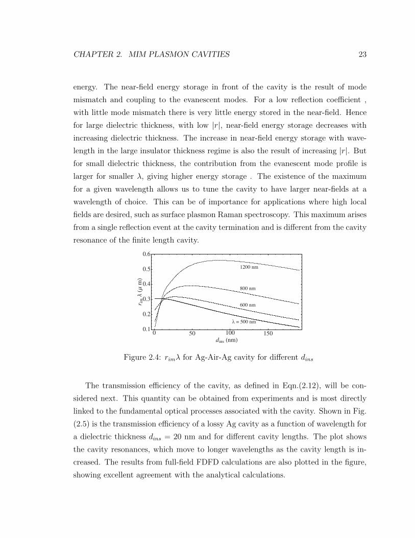
CHAPTER 2. MIM PLASMON CAVITIES 23
energy. The near-field energy storage in front of the cavity is the result of mode
mismatch and coupling to the evanescent modes. For a low reflection coefficient ,
with little mode mismatch there is very little energy stored in the near-field. Hence
for large dielectric thickness, with low |r|, near-field energy storage decreases with
increasing dielectric thickness. The increase in near-field energy storage with wave-
length in the large insulator thickness regime is also the result of increasing |r|. But
for small dielectric thickness, the contribution from the evanescent mode profile is
larger for smaller λ, giving higher energy storage . The existence of the maximum
for a given wavelength allows us to tune the cavity to have larger near-fields at a
wavelength of choice. This can be of importance for applications where high local
fields are desired, such as surface plasmon Raman spectroscopy. This maximum arises
from a single reflection event at the cavity termination and is different from the cavity
resonance of the finite length cavity.
Figure 2.4: rimλ for Ag-Air-Ag cavity for different dins
The transmission efficiency of the cavity, as defined in Eqn.(2.12), will be con-
sidered next. This quantity can be obtained from experiments and is most directly
linked to the fundamental optical processes associated with the cavity. Shown in Fig.
(2.5) is the transmission efficiency of a lossy Ag cavity as a function of wavelength for
a dielectric thickness dins = 20 nm and for different cavity lengths. The plot shows
the cavity resonances, which move to longer wavelengths as the cavity length is in-
creased. The results from full-field FDFD calculations are also plotted in the figure,
showing excellent agreement with the analytical calculations.

CHAPTER 2. MIM PLASMON CAVITIES 24
Figure 2.5: Transmission efficiency (Teff ) through a Ag-Air-Ag cavity for differentcavity lengths (L) as a function of wavelength.
The cavity resonance length (Lres) for different resonance orders, as a function of
dielectric thickness is plotted in Fig. (2.6). The good correspondence between the
analytical calculation and the full-field simulations confirm the validity of our model
for the considered parameters. From the figure it can be seen that the resonant
length calculations made by ignoring the phase pickup on reflection (dotted lines)
would result in substantial error, especially at higher dielectric thicknesses. Another
interesting feature in the plots is the relatively weak dependence of the resonance
length on the dielectric layer thickness for sufficiently large thicknesses (> 50 nm).
This can be understood from in Eqn.(2.13), which shows that the resonance length
is dependent on two factors: 1) the gap SPP wavelength and 2) the phase pickup
on reflection. As the dielectric layer thickness is increased, the gap SPP wavelength
increases and approaches that of the single interface mode. As the same time, the
reflection phase also increases. As the effects of an increased wavelength and phase
work in opposite directions, the resonant length stays more-or-less the same.
As the dielectric thickness is reduced in an MDM cavity, the symmetric SPP mode
is more confined resulting in a very small mode volume. This is very advantageous
for active plasmonic devices allowing for example, efficient coupling of quantum emit-
ters to SPP gap modes in MDM cavities [13]. Strong emission rate enhancement
is also predicted even for non-resonant conditions in an infinite length MDM slab

CHAPTER 2. MIM PLASMON CAVITIES 25
Figure 2.6: Cavity resonance length as a function of dielectric thickness for differentorders. Free space wavelength λ=900nm. (Ag-Air-Ag cavity with loss.)
Figure 2.7: Q-factor of the cavity vs cavity length for different dielectric thicknesses.Free space wavelength λ=800nm. Ag-Air-Ag cavity with loss
geometry[51]. The transmission cross section can be used to calculate the quality fac-
tor (Q) of the finite length MDM cavities. Shown in Fig.(2.7) is a plot of Q vs cavity
length for different dielectric thicknesses at λ = 800nm for Ag-Air-Ag MDM cavity
with metal losses included. The cavity Q increases with length, showing evidence of
being reflection loss limited. This is true even for dielectric thickness as low as 10 nm
with cavity lengths as large as 1500 nm, demonstrating that propagation loss is not
the dominating loss mechanism in these cavities. This suggests the possibility of in-
creasing the quality factor of these cavities further by end face shaping thus realizing
very low reflection losses. Such a device will exhibit larger Q/V values and enable
CHAPTER 2. MIM PLASMON CAVITIES 26
very effective coupling of optical emitters to a well-defined SPP mode.
2.3 Conclusion
In conclusion we have developed a fully analytical theory for SPP resonances in finite-
length MDM cavities. It builds on previous results that indicate that a variety of
wavelength scale plasmonic systems can be viewed as resonators for SPPs[34, 46, 42].
Such a model requires knowledge of the basic optical properties of SPP modes sup-
ported by an extended MDM waveguide and the SPP reflection and transmission
properties at the termination of such a waveguide. We have presented an analyt-
ical framework to determine these properties for cavities consisting of real metals
exhibiting loss and dispersion. Similar to what was found for other wavelength-scale
plasmonic cavities, these calculations predict a substantial phase pick up by the SPP
upon reflection from the cavity end faces. We showed that the origin of this phase
pick up lies in the excitation of evanescent modes in free space region just outside the
cavity. Furthermore, we found that the imaginary part of the reflection coefficient is
proportional to the energy storage in the near-field of the cavity termination. From
the calculation of this phase pick up one can correctly predict both the position and
shape of the MDM cavity transmission resonances over a wide range of wavelength
and geometric parameters. The results agree very well with full-field FDFD simula-
tions. The dependence of the quality factor on the length of the cavity shows that
these resonances are reflection loss limited even at very small dielectric thickness and
suggests the possibility of further improving the quality factor of these resonances by
end face shaping.

Chapter 3
Surface Plasmon Patch Antenna
In the previous chapter, we looked at plasmon resonances and energy storage in a
truncated MDM cavity with infinitely thick metals separated by a dielectric. Optical
devices based on this geometry have finite metal thickness, and the additional metal
surface opens up the possibility of further tailoring the optical properties through
mode interaction. In this chapter we explore a novel dual purpose patch antenna in the
optical regime. Metal patch antennas have been studied in the past as good candidates
for single photon emission sources [71], and have also attracted a lot of attention lately
for their applicability in meta surface structures[72, 73]. However, traditionally metal
antennas in optical frequencies have exploited a single mode plasmon resonance for
its action[34]. We demonstrate an optically excited plasmon source which exploits
the interference action of a two-path two-mode resonance to function as an effective
radiative antenna. The interference action of the two modes provides for an additional
level of control over the antenna emission characteristic. This allows us to efficiently
change the resonance characteristics of the cavity to use it either as an efficient single
lobed radiator, a directional emitter or an excellent plasmon coupler. A large fraction
of the cavity round trip phase pickup needed for resonance is accommodated by the
reflection phase, resulting in an extremely compact device much smaller than the
effective plasmon wavelength in the structure.
27

CHAPTER 3. SURFACE PLASMON PATCH ANTENNA 28
Fulfilling the promise of a complete surface plasmon based optical circuit re-
quires compact devices that can excite as well as route surface plasmons and me-
diate energy transfer between near and far fields. Recent efforts in the field have
resulted in plasmonic antennas based on meta-material structures[74], and Yagi-Uda
like designs[75, 76, 77] for for a variety of applications. Various configurations of
plasmon waveguides, that have effectively optimized the tradeoff between mode con-
finement and propagation loss, have been explored in the past. [78, 79, 80, 81, 82, 83].
Many different optical and electrical plasmonic sources have also been demonstrated
including those with silicon[22] and organic semiconductors[84]. An optical antenna
is another necessary component needed for the concentration of light to enhance
the interaction between propagating wavelength dimensions and device scale. They
have found extensive use in scattering[85], redirecting[86], and enhancement of op-
tical fields[87] for a variety of applications[88]. For a complete plasmonic circuit,
however, one needs a device geometry that not only can be tailored to fit many of
these different roles but also is amenable to easy fabrication. Here, we demonstrate a
metal insulator multilayer device with a geometry which can be very easily tailored
to function in all these roles very effectively.
Resonances in truncated metal stripe waveguides in a dielectric background have
been studied extensively in the past[89, 42]. The plasmon mode resonance occurs in
these structures when the round trip phase pick up, due to propagation and end face
reflections, add up to an integral multiple of 2π. The thickness and length of the stripe
is chosen to allow resonance of a single mode at the desired wavelength. This mode
is excited through a variety of optical and electrical methods. However, the closely
spaced metal surfaces in a metal stripe antenna or a stripe patch antenna above a
metal ground plane allow for multiple modes with different field symmetries. All these
modes can be simultaneously excited and though they propagate independently, they
can interact through reflection at the antenna terminations. These interactions can
be constructive or destructive and lead to preferential transmission or reflection into
some modes while inhibiting power coupled into the others.
CHAPTER 3. SURFACE PLASMON PATCH ANTENNA 29
3.1 Sample fabrication and experiment details
An SEM image and a schematic showing the basic device design is shown in Fig.
(3.1a,b). It consists of a silver stripe patch antenna over a silver ground plane sep-
arated by a spacer layer of alumina. Quantum dots (CdSe-ZnS core-shell) dispersed
in the alumina layer illuminated by an excitation laser emit into the plasmon modes.
These type-1 quantum dots were chosen for their good photo-stability and high emis-
sion quantum efficiency. The quantum dots below the stripe antenna, are sandwiched
between the stripe and the ground plane. This enhances its emission rate into the
gap plasmon mode that has high intensity fields in the alumina region.
L
H
D
Detector
Pinhole
Ar ion Laser
(a)
(b)
(c)
Figure 3.1: (a) SEM of the stripe antenna structure. White bar is 5µm (b) Aschematic of the device geometry. Thickness D = 40 nm, H = 50 nm, L = 140nm - 340 nm. A rendering of illuminating Ar-ion beam and the two lobed antennaemission is shown (c) Confocal measurement set up. The illuminating laser and thecollected PL is polarized perpendicular to the stripe. Dichroic filter removes theillumination beam from the collected signal.
Silver ground plane film layer (150nm) is deposited with e-beam evaporation on
polished Si wafer substrate immediately followed by a 10nm coating of alumina by
atomic layer deposition with trimethyl aluminum hydroxide and water. Quantum

CHAPTER 3. SURFACE PLASMON PATCH ANTENNA 30
Figure 3.2: Photograph of the Witec Alpha SNOM system
dots (Ocean Nano CdSe-ZnS core-shell) are put down by spin coating from a toluene
solution followed by another 10 nm layer of alumina deposition (Low temperature
ALD at 80◦C.) The metallic antenna structures are fabricated by standard e-beam
lithography lift-off with a protective layer of 10nm AlOx covering the whole structure.
The emission characteristics of the quantum dots were confirmed to be unchanged
by PL measurements before and after the fabrication process. A Witec alpha 300s
SNOM system, shown in Fig. (3.2) was used for the confocal scans with a 100X
mitutoyo (0.9 NA) objective to illuminate and collect during the scans. The scattered
PL was collected in a confocal scan mode as shown in Fig. (3.3a) . We employ a
slight modification on this standard confocal scan configuration to also study surface
plasmon scattering from the antenna as described in section[3.3]. In a normal confocal
scan geometry the illumination and collection is from the same spot on the sample. In
contrast to this, for surface plasmon scattering we excite the plasmons at a distance,
s = 7.5µm away from the antenna, but collection of the scattered radiation is focused

CHAPTER 3. SURFACE PLASMON PATCH ANTENNA 31
on a spot above the antenna. A schematic of this configuration is shown in Fig.
(3.3b).
s
a) b) In focus fluorescent emission Out of focus fluorescent emission
In focus fluorescent emission Out of focus fluorescent emission
Objective lens Objective lens
Out of focus focal plane Out of focus focal plane
In-focus focal plane
Confocal Pin hole
Staggered Confocal Pin hole
Figure 3.3: Schematic of the confocal scan configuration a) Standard confocal b)Staggered confocal. Illumination at a distance s = 7.5µm away from the collectionspot on the sample.

CHAPTER 3. SURFACE PLASMON PATCH ANTENNA 32
150 nm Ag E-beam evaporation. Si substrate
10 nm AlOx ALD Protect Ag from oxidation
Spin on Q dots CdSe/ZnS core-shell Approx 10nm diameter
20 nm AlOx ALD Total insulator thickness =40nm
Antenna: Ag :40nm thick 140-340nm width E-beam litho, lift-off
ALD AlOx 10nm Protective coating
Figure 3.4: Schematic of fabrication process
3.2 Scattering under normal illumination
First, we take a look at the device’s antenna characteristics, and we employ a confocal
scan to study the beam shape of the emission. The stripe region is illuminated by
the defocused excitation laser (Ar-ion 514nm) polarized perpendicular to the stripe
length and an X-Z confocal scan of the emitted photoluminescence (PL) is performed.
Figure (3.5) shows the radiation pattern from the antenna for stripe widths from 140
nm - 340 nm. The antenna emission pattern evolves from a single lobe emission in
smaller width stripes, with the excitation of lowest order resonance, to a two lobed
emission in larger stripes, exciting higher order modes. It should be noted that the
scan images are normalized to the maximum intensity for each stripe. Figure[ 3.6]
shows the normalized scans for the stripes normalized to the maximum intensity from
the 140 nm stripe. The absolute intensity at 340 nm antenna length is about 25 %
of the intensity at 140 nm.
In order to understand the radiation properties, we need to study the plasmon
modes in the structure. Like all metallic antennas in the optical regime, the transfer of

CHAPTER 3. SURFACE PLASMON PATCH ANTENNA 33
0 1 2 3 4 5x µm
0
1
2
3
4
5
6
z µm
140nm
0 1 2 3 4 5x µm
0
1
2
3
4
5
6 160nm
0 1 2 3 4 5x µm
0
1
2
3
4
5
6 180nm
0 1 2 3 4 5x µm
0
1
2
3
4
5
6 200nm
0 1 2 3 4 5x µm
0
1
2
3
4
5
6
z µm
220nm
0 1 2 3 4 5x µm
0
1
2
3
4
5
6 240nm
0 1 2 3 4 5x µm
0
1
2
3
4
5
6 260nm
0 1 2 3 4 5x µm
0
1
2
3
4
5
6 280nm
0 1 2 3 4 5x µm
0
1
2
3
4
5
6
z µm
300nm
0 1 2 3 4 5x µm
0
1
2
3
4
5
6 320nm
0 1 2 3 4 5x µm
0
1
2
3
4
5
6 340nm
Min
0.25
0.5
0.75
Max
Figure 3.5: Confocal scans of stripe antennas under de-focused normal illumination.Length of the stripes is shown for each scan image
energy between the near and far field is mediated by surface plasmons. A schematic
of the magnetic field for various plasmon modes in the structure is given in Fig.
(3.7a). The presence of the ground plane breaks the symmetry of the modes that
would have existed in an isolated metallic stripe. We do not have purely symmetric
and anti-symmetric modes in the patch antenna. The two modes of relevance for the
CHAPTER 3. SURFACE PLASMON PATCH ANTENNA 34
0 1 2 3 4 5x µm
0
1
2
3
4
5
6
z µm
140nm
0 1 2 3 4 5x µm
0
1
2
3
4
5
6 160nm
0 1 2 3 4 5x µm
0
1
2
3
4
5
6 180nm
0 1 2 3 4 5x µm
0
1
2
3
4
5
6 200nm
0 1 2 3 4 5x µm
0
1
2
3
4
5
6
z µm
220nm
0 1 2 3 4 5x µm
0
1
2
3
4
5
6 240nm
0 1 2 3 4 5x µm
0
1
2
3
4
5
6 260nm
0 1 2 3 4 5x µm
0
1
2
3
4
5
6 280nm
0 1 2 3 4 5x µm
0
1
2
3
4
5
6
z µm
300nm
0 1 2 3 4 5x µm
0
1
2
3
4
5
6 320nm
0 1 2 3 4 5x µm
0
1
2
3
4
5
6 340nm
Min
0.25
0.5
0.75
Max
Figure 3.6: Confocal scan of the stripe antenna with the maximum intensity normal-ized to the emission intensity from the 140 nm stripe.
device dimensions of interest have predominantly MIM mode shape (field maxima in
the insulator region between the stripe and the ground plane) and IMI mode shape
(field maxima at the top of the metallic stripe). In this context the metallic antenna
can be thought of as a plasmonic cavity with the cavity reflection coefficient and
resistive losses determining the antenna efficiency. Here the vertical confinement of

CHAPTER 3. SURFACE PLASMON PATCH ANTENNA 35
the plasmon mode is determined by the insulator and metal thickness, which also
controls the plasmon reflection coefficient from the cavity end faces. Shown in Fig.
(3.7 b) is the calculated mode index of the MIM mode, where as, Fig. (3.7 c-d) show
the propagation length of the MIM and IMI modes respectively as function of alumina
thickness (D) and antenna thickness (H). The mode indices and propagation lengths
are calculated using the reflection pole method[90]. For simulations εAg = −13.73 −1.15i at 620 nm is taken from Rakic et al [91] and εAlumina = 2.72. For efficient coupling
of quantum dot emission to the plasmon modes and to increase the cavity reflection
coefficient it is attractive to increase the mode index by decreasing the insulator
thickness. But this increase in confinement comes at the cost of decreased propagation
length of the plasmon modes. To obtain a balance of high mode confinement and low
propagation loss, values for D and H were both chosen to be 40 nm for the experiments.

CHAPTER 3. SURFACE PLASMON PATCH ANTENNA 36
(a)
(b)
(c)(d)
0
1
Ground Plane
Antenna
2
D
H
Figure 3.7: (a) Schematic of Hy field profile for the various plasmon modes in thestructure: 0 - Ground plane mode, 1- MIM mode and 2- IMI mode. (b) Mode index(λ0/λ for the MIM mode as a function of the antenna thickness (H) and spacerthickness (D) at 620 nm. (c,d) Propagation length in nm for the MIM mode and IMImode respectively.
3.3 Plasmon interference in patch antenna struc-
tures
To exploit the interference aspect of the antennas optical response we illuminate the
antenna with a ground plane plasmon mode and study its response with confocal
microscopy. Figure (3.8a) shows the schematic of the surface plasmon scattering
experiment configuration. A plasmon mode is excited at a distance of around 7.5µm
from the stripe by illuminating the quantum dots with a focused beam. The excitons

CHAPTER 3. SURFACE PLASMON PATCH ANTENNA 37
in the quantum dots relax to the plasmon mode on the antenna ground plane. This
plasmon mode propagates to the antenna structure and is scattered to free space
radiation modes. A fraction of the incident plasmon energy is reflected back and
transmitted through the antenna into the ground plane plasmon modes as well. This
however is not picked up in the scans as confocal scans can only measure the fraction
of energy that is scattered into radiation modes within the numerical aperture of the
collection objective.
x nm
y n
my n
m
x nm
y n
m
x nm
a) b)
c) d)
Figure 3.8: (a) Schematic of the plasmon scattering experiment setup. (b-d)|H| fromFDFD simulation of plasmon scattering for different stripe widths (b) L = 160 nm(c) L = 280 nm (d) L=320nm
Full field FDFD simulations, Fig. (3.8 b-d), where surface plasmon polariton is
incident from the left on to a patch antenna show the scattering field pattern of the
antenna for various antenna lengths. Majority coupling to the forward lobe and weak
emission through the backward lobe can be observed in the simulations for longer
stripes. Confocal scans (shown in Fig. (3.9) ) show the directional scattering of
the plasmon modes for various antenna stripe lengths. The radiation mode pattern

CHAPTER 3. SURFACE PLASMON PATCH ANTENNA 38
is mostly unperturbed for smaller stripe widths, compared to the scattering under
normal illumination. Under asymmetric illumination with a surface plasmon mode,
the two lobed pattern observed for longer antennas is no longer observed, and is
replaced by a forward scattering single lobe. This is a clear evidence of the antenna
being reflection loss limited as opposed to being limited by resistive losses in the
cavity. Similar to the observation in the normal illumination confocal scans, the
stripes at longer widths scatter weakly and the maximum intensity at stripe length of
340nm is approximately 25% of that at 140nm. In order to understand the amplitude
behavior of the scattering spectra we need to understand the scattering process in
these antennas. This is most accurately achieved through FDFD and a near to far
field transform to see the radiation pattern, but this does not provide intuition into
the physical mechanism of scattering. So in the next section, we derive a multi-
path interference model for the scattering amplitudes for a patch antenna through a
semi-analytical mode matching technique.

CHAPTER 3. SURFACE PLASMON PATCH ANTENNA 39
0 1 2 3 4 5x µm
0
1
2
3
4
5
6
z µm
140nm
0 1 2 3 4 5x µm
0
1
2
3
4
5
6 160nm
0 1 2 3 4 5x µm
0
1
2
3
4
5
6 180nm
0 1 2 3 4 5x µm
0
1
2
3
4
5
6 200nm
0 1 2 3 4 5x µm
0
1
2
3
4
5
6
z µm
220nm
0 1 2 3 4 5x µm
0
1
2
3
4
5
6 240nm
0 1 2 3 4 5x µm
0
1
2
3
4
5
6 260nm
0 1 2 3 4 5x µm
0
1
2
3
4
5
6 280nm
0 1 2 3 4 5x µm
0
1
2
3
4
5
6
z µm
300nm
0 1 2 3 4 5x µm
0
1
2
3
4
5
6 320nm
0 1 2 3 4 5x µm
0
1
2
3
4
5
6 340nm
Min
0.25
0.5
0.75
Max
Figure 3.9: Confocal scans for the stripe antenna of different lengths illuminated witha focused spot at a distance of 7.5µm to the left of the antenna. The intensity ineach image is normalized to the maximum intensity in the scan. The plasmon isincident on the stripe from the left and the resulting radiation from the antenna isasymmetric.
CHAPTER 3. SURFACE PLASMON PATCH ANTENNA 40
0 1 2 3 4 5x µm
0
1
2
3
4
5
6
z µm
140nm
0 1 2 3 4 5x µm
0
1
2
3
4
5
6 160nm
0 1 2 3 4 5x µm
0
1
2
3
4
5
6 180nm
0 1 2 3 4 5x µm
0
1
2
3
4
5
6 200nm
0 1 2 3 4 5x µm
0
1
2
3
4
5
6
z µm
220nm
0 1 2 3 4 5x µm
0
1
2
3
4
5
6 240nm
0 1 2 3 4 5x µm
0
1
2
3
4
5
6 260nm
0 1 2 3 4 5x µm
0
1
2
3
4
5
6 280nm
0 1 2 3 4 5x µm
0
1
2
3
4
5
6
z µm
300nm
0 1 2 3 4 5x µm
0
1
2
3
4
5
6 320nm
0 1 2 3 4 5x µm
0
1
2
3
4
5
6 340nm
Min
0.25
0.5
0.75
Max
Figure 3.10: Confocal scans for the stripe antenna of different lengths illuminatedwith a focused spot at a distance of 7.5µm to the left of the antenna. The intensity ineach image is normalized to the maximum intensity for 140nm stripe. The plasmonis incident on the stripe from the left and the resulting radiation from the antenna isasymmetric.

CHAPTER 3. SURFACE PLASMON PATCH ANTENNA 41
3.4 Coupled cavity model for plasmon scattering
The scattering property of the antenna and its interference action can be best un-
derstood by studying the interaction between antenna plasmon modes in the cavity.
A complete description of the stripe ground plane system will involve the excita-
tion and interaction between all the possible discrete and continuum surface plasmon
modes. But a basic understanding of the antenna characteristics can be achieved
by modeling the antenna as a surface plasmon cavity with discrete modes. The two
distinct degenerate plasmon modes possible in this structure at dimensions of inter-
est (MIM and IMI) have energy concentrated at different interfaces and have very
different wave numbers. These modes interact through scattering at the cavity end
faces. In addition, they couple to both the radiation channel (free space modes) and
the ground plane plasmon mode (GP). The strength of coupling to the radiation
channel competes with the coupling to the bound plasmon modes. When the ground
plane plasmon mode is incident on the antenna, the two antenna modes are excited
(MIM and IMI). These modes couple to each other through reflection at the end faces,
and propagate independently with energy concentrated at different interfaces . We
can model this as coupled Fabry-Perot cavities, where the difference in the reflection
phase pick up and the mode index of the two modes, lead to constructive or destruc-
tive transmission to the ground plane plasmon mode out of the cavity for different
antenna lengths. Such Fabry-Perot models have been shown to be very effective in
modeling plasmonic cavity and antenna structures[92, 93].
The patch antenna can be decomposed into two Fabry Perot cavities as shown in
Fig. (3.11). We consider the ground plane plasmon incidence on the patch antenna
and derive the transmission and reflection coefficients for the GP mode. When the GP
mode transmits through the patch antenna stack, it goes through two parallel paths,
each with differing strengths and acquired phase. The resultant interference can be
predicted by the model provided all the coupling coefficients can be calculated. For
the three modes of interest there are 6 coupling coefficients that we need to calculate.
The coupling coefficient between two modes i and j is denoted by rij for reflection
and tij for transmission, as shown in the Fig. (3.11). They can be calculated from a

CHAPTER 3. SURFACE PLASMON PATCH ANTENNA 42
r11
r12
r21
r22 t20
t10
r00
mode 1: MIM
mode 2 : ASYM mode 0
mode 0 E1
E2
t01
t02
Stripe
Ground plane Cavity 1
Cavity 2
Figure 3.11: Two cavity model.
field decomposition at appropriate truncations of a one dimensional geometry. When
a plasmon mode (GP, MIM, IMI) is incident on a structure discontinuity, it reflects
and transmits into all the possible modes on either side of the interface. The total
electric field on either side of the interface can be written as a sum over all the possible
orthogonal modes,
Etotal =∑modes
cmodeEmode (3.1)
FDFD simulation of this scenario can generate the total field profile, and we can then
use orthogonality relations of the modes on either side of the interface to determine
the coefficient cmode. We can now ignore the scattering into the radiation modes and
only look at coupling between the 3 modes of interest. From the numerically calcu-
lated coupling coefficients between the modes at the patch antenna truncation, we
can derive a coupled cavity model for transmission through the patch antenna as a

CHAPTER 3. SURFACE PLASMON PATCH ANTENNA 43
0 100 200 300 400 500 600L antenna
0.0
0.2
0.4
0.6
0.8
1.0
R,T
Ta
R a
T f
R f
S f
I r
Figure 3.12: Transmission and reflection spectra for ground plane surface plasmonincident on stripe antenna. Tf , Rf from full field simulations and Ta, Ra from theanalytical model (Details in appendix). Scattered intensity assuming no loss in thecavity, Sf = (1−Tf−Rf ), is also plotted. The measured maximum radiated intensityin the staggered confocal scan is normalized and overlaid on this plot (Ir). Thescattered intensity calculation can be seen to be correctly predicting the measuredintensity for a range of stripe lengths.
function of cavity length. Transmission and reflection coefficients out of the cavity
are derived in appendix C. The validity of this simple model for antenna scattering
is proven through full field simulations. In Fig. (3.12i) we have plotted transmission
and reflection from a patch antenna as function of antenna length, calculated with
FDFD simulations. Also, plotted are the transmission and reflection results from the
coupled cavity model. The semi-analytical model calculations reproduce all the es-
sential features of the full field simulations. There is a small difference in magnitude
of the calculated transmission and reflection, especially at low cavity lengths. This
is to be expected as we ignored the coupling between the free space modes (propa-
gating and evanescent) and the cavity modes. The resulting error will be larger for
smaller cavities and can be expected to reduce with increasing cavity lengths, due to
evanescent and spherical divergence decay of the ignored field amplitudes.
We can also compare the results directly with the experimental results if we ignore

CHAPTER 3. SURFACE PLASMON PATCH ANTENNA 44
losses in the cavity. In the absence of resistive losses in the cavity the difference
between the incident power (normalized to unity) and the total coupled power into the
ground plane plasmon mode (Rf +Tf ) is the scattering into the radiation modes. The
calculated scattered energy assuming no loss in the cavity (1− (Tf +Rf )) agrees very
well with the measured normalized scattered intensity. For ease of comparison the
scattered intensity plot is overlaid on the analytical calculations so that the maxima
of the two coincide. The experimental results closely follow the analytical calculations
for small stripe lengths. For larger stripe lengths the experimental results drop below
the analytical calculations. This is to be expected as in longer antennas the cavity
losses can no longer be neglected and the analytically calculated scattering energy that
assumes zero loss will over estimate the scattering strength. The mode propagation
losses can be estimated and subtracted from the total loss to get a better estimate
of the scattering strength of the cavity. There are several other interesting features
in this transmission spectra. At an antenna length of around 160 nm, as shown
in Fig. (3.13a,b) both transmission and reflection simultaneously decrease, due to
destructive interference of the two antenna modes. This increase in the coupling to
the radiative channel makes this an ideal length for a radiating antenna. At around
L = 280 nm, as shown in Fig. (3.13c,d) the constructive interference of the antenna
modes, leads to near zero reflection and enhanced transmission. This is a good length
for a plasmon source that efficiently excites the ground plane plasmon mode. The
peak of the advancing wavefronts also show the shallower angle of emission in the 280
nm long stripe compared to the 160 nm stripe as is confirmed by the experiments. It
should be noted that in addition to the difference in the reflection phase pick up of
the two plasmon modes, the coupling between the modes at the cavity termination
is necessary to account for the interference effects. Moreover, for good modulation of
the reflection and transmission coefficients we need the total power in the two cavity
modes to be approximately the same, through near equal excitation from the ground
plane mode or through good coupling between the modes due to reflections at the
cavity terminations.
In this chapter we have shown that a metallic patch antenna in the optical regime
is a versatile design which can be easily tailored to function as a plasmon source,

CHAPTER 3. SURFACE PLASMON PATCH ANTENNA 45
X nm
X nm
Z n
mZ n
m
X nm
X nm
Z n
mZ n
m
c)
g)
a)
c)
b)
d)
Figure 3.13: (a) Re[Hy] for 160nm antenna length. The decreased transmission can beclearly seen. (b) Simulated |Hy| for plasmon scattering from a 160 nm long antenna.The fields are normalized for unit amplitude of incident mode field maxima. Thecolormap scale is clipped to clearly show the antenna radiation mode profile. (c)Re[Hy] for 280 nm antenna length. The enhanced transmission due to the constructiveinterference from the two arms can be clearly observed (d) Simulated |Hy| for 280 nmantenna.
radiator or a directional antenna. Here, multiple plasmon modes in the structure
interact to facilitate enhanced optical response under various illumination conditions.
The design can be optimized for energy transfer from localized wavelength or device
dimensions to propagating far field wavelength scale while reducing intrinsic losses.
The same structure can also be used for in-plane surface plasmon interferometric
sensing applications as the resonance conditions are very sensitive to the refractive
index changes near the metal stripe antenna. A very simple analytical scattering
model that explains all the essential features of this plasmon antenna structure is
derived and validated with full field simulations and experimental results.

Chapter 4
Electrical Modulation of Surface
Plasmon Coupled Emission
4.1 Introduction
In the previous chapter we looked at scattering of plasmons by metallic antennas,
thereby probing the optical functionality of these devices. In this chapter we look
at dual-purposing the same metallic antennas as electrical leads, and demonstrate an
active plasmonic device based on MDM geometry. The patterned metallic electrodes
in an MDM cavity can serve as the contact pads as well as the optical element
in a device that is electrically pumped for light emission. The proximity of the
metallic surfaces to the active regions of the device, enhances the electron-hole pair
recombination rate by coupling the energy to plasmon modes, greatly increasing the
internal quantum efficiencies. This has been exploited in a number of plasmon assisted
light emitting devices like Quantum Well light emitting diodes (LED)[94] and Organic
LEDs. [95, 84].
Here, we look at a quantum dot light emitting device based on the patch antenna
geometry discussed in chapter [3] and demonstrate active electrical control over its
emission intensity and wavelength. We apply a voltage across the patch antenna -
quantum dot structure, and utilize Quantum Confined Stark Effect (QCSE)[96] to
shift its emission wavelength. The small foot print and ease of fabrication of such a
46

CHAPTER 4. ELECTRICAL MODULATION 47
device makes it a prime candidate for a nanoscale surface plasmon source.
4.2 Sample fabrication and experiment details
In this section we will outline the fabrication and experimental details for the surface
plasmon QCSE modulator. The fabrication of the device parallels that of the patch
antenna structure with some minor differences. Silver ground plane film layer (150
nm) is deposited with e-beam evaporation on polished Si wafer substrate immediately
followed by a 10 nm coating of alumina by atomic layer deposition with trimethyl
aluminum hydroxide and water. Quantum dots (Ocean Nano CdSe-ZnS core-shell)
are put down by spin coating from a toluene solution followed by another 10 nm layer
of alumina deposition by ALD. The metallic antenna structures are fabricated by
standard e-beam lithography lift-off with a protective layer of 10 nm AlOx covering
the whole structure. An SEM image of the antenna structure and a schematic of the
measuring setup is shown in Fig. (4.1) Here, unlike in the normal patch antenna
structure, we require a high quality ALD oxide to enable application of electrical bias
without breakdown. For a good electrical insulator AlOx, with low defect density, the
ALD growth must be performed at high temperatures[97]. However, the quantum dots
which will need to be sandwiched between the oxide layers have a polymer coating that
may degrade these temperatures. These organic coatings are proprietary and exact
details of the thermal stability characteristics could not be determined. The vendor
supplied tolerable highest temperature (<70◦C) seemed to be overly conservative, as
these quantum dots were unaffected by the ALD deposition at 80◦C. The quantum
dots deposited by spin coating from a toluene solution on to silicon substrates and
were annealed at temperatures from 130◦C to 300◦C. As can be seen from Fig. [4.2],
for temperatures less than 200◦C the changes in the PL spectra of the quantum dots
were insignificant. However, since the annealing was only done for 10 minutes for each
sample, in order to avoid any effect from longer time exposure to high temperatures
we decided to perform the ALD at 100◦C. The PL spectra taken after the fabrication
of the stack show no change in width or emission center wavelength compared to
emission from an initial sample of quantum dots. For Stark shift measurements, the
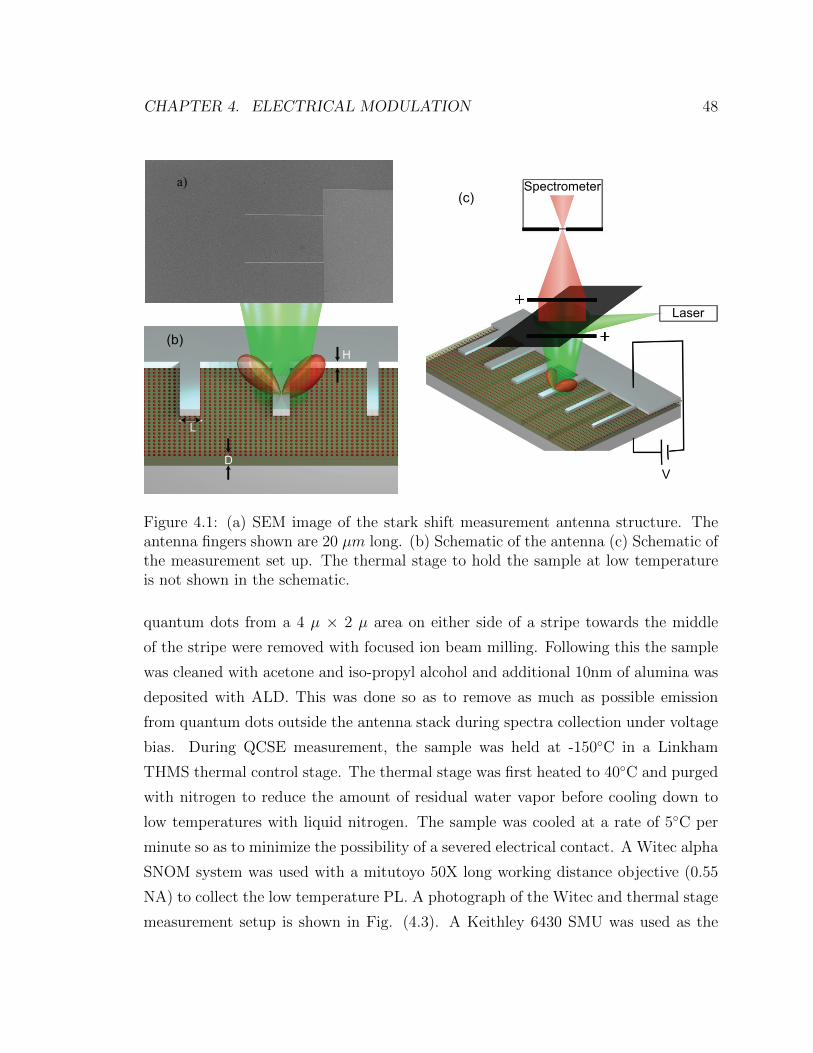
CHAPTER 4. ELECTRICAL MODULATION 48
L
H
D
Laser
Spectrometer
V
(b)
(c)
a)
Figure 4.1: (a) SEM image of the stark shift measurement antenna structure. Theantenna fingers shown are 20 µm long. (b) Schematic of the antenna (c) Schematic ofthe measurement set up. The thermal stage to hold the sample at low temperatureis not shown in the schematic.
quantum dots from a 4 µ × 2 µ area on either side of a stripe towards the middle
of the stripe were removed with focused ion beam milling. Following this the sample
was cleaned with acetone and iso-propyl alcohol and additional 10nm of alumina was
deposited with ALD. This was done so as to remove as much as possible emission
from quantum dots outside the antenna stack during spectra collection under voltage
bias. During QCSE measurement, the sample was held at -150◦C in a Linkham
THMS thermal control stage. The thermal stage was first heated to 40◦C and purged
with nitrogen to reduce the amount of residual water vapor before cooling down to
low temperatures with liquid nitrogen. The sample was cooled at a rate of 5◦C per
minute so as to minimize the possibility of a severed electrical contact. A Witec alpha
SNOM system was used with a mitutoyo 50X long working distance objective (0.55
NA) to collect the low temperature PL. A photograph of the Witec and thermal stage
measurement setup is shown in Fig. (4.3). A Keithley 6430 SMU was used as the

CHAPTER 4. ELECTRICAL MODULATION 49
560 580 600 620 640 660 680Wavelength (nm)
0
5000
10000
15000
20000
25000
30000
35000
Inte
nsi
ty (
AU
)
No Anneal130 C200 C250 C300 C
Figure 4.2: The PL spectra from quantum dots after annealing at various tempera-tures.
voltage source for the measurements. The sample was illuminated by a 514nm Ar-Ion
laser with the beam polarized perpendicular to the stripe width.
Figure 4.3: Photograph of the thermal stage mounted on the Witec SNOM

CHAPTER 4. ELECTRICAL MODULATION 50
4.3 Quantum Confined Stark Effect
Figure[4.4] shows the voltage bias dependent PL emission spectra from the quantum
dots in the patch antenna. The emission broadens and the peak of the emission is
red shifted. This can be explained as arising from the quantum confined stark effect.
The shifting of the energy levels in the quantum dots due to the applied electric
field lowers the electron hole recombination energy, and the resulting emission is
at a longer wavelength. The application of voltage bias also causes a reduced PL
efficiency in the quantum dots. The electrons and holes are physically separated in
the quantum dot, reducing the wave function overlap and the recombination cross-
section. Also, the large fields could dissociate the electron-hole pairs and the free
carriers can facilitate non radiative recombination, further increasing the luminescence
quenching. It should be noted that consistent with Stark effect, the reduced emission
at the center wavelength is accompanied by a slight increase in emission intensity at
longer wavelength. This is consistent with other observations of Stark effect in CdSe
quantum dots [98]. The Stark shift in emission energy ∆E is given by perturbation
theory to be
∆E = −µF − αF 2 + · · · (4.1)
Here µ is the built in polarization of the quantum dot, α is the polarizability of the
quantum dots and F is the internal electric field in the quantum dot. Even though
the Cd-Se quantum dots have a Wurtzite crystal structure and an associated built in
dipole moment, we do not expect to see the linear contribution of the Stark effect.
This is because the measured PL is an ensemble average of the quantum dots with all
possible orientations in the patch antenna structure. We can hence fit the emission
shift to a quadratic function to determine the polarizability of the quantum dots. The
electric field inside the quantum dot was calculated as,
F =3
εQD
εd+ 2
F0 =3
εQD
εd+ 2
V
d(4.2)

CHAPTER 4. ELECTRICAL MODULATION 51
560 580 600 620 640 660 680Wavelength (nm)
0.0
0.2
0.4
0.6
0.8
1.0
Norm
aliz
ed P
L0V3V6V9V
Figure 4.4: PL spectra of the quantum dots in the patch antenna structure for variousbias voltages.
Here, εQD and εd are the dielectric constants and V is the applied voltage across the
dielectric of thickness d = 40 nm. The values of the dielectric constants chosen were
εQD = 9.2 and εd = 2.25. A plot of emission peak energy shift as a function of the
internal electric field is given in Fig. (4.5). The peak shift shows a quadratic increase
at low electric fields, 10 meV at around 600 kV/cm, with sub-quadratic increase
at higher electric fields. Fit to the peak energy shift data gives a polarizability of
α ≈ 3.2× 10⁻⁵.
In this chapter we have demonstrated experimentally a simple active plasmonic
antenna, based on the MDM geometry. The high field enhancement in the dielectric
region due to the plasmon modes, enhances the quantum dot emission. The ease

CHAPTER 4. ELECTRICAL MODULATION 52
0 200 400 600 800 1000 1200 1400F (Electric Field kV/cm)
0
5
10
15
20
25
30
35
40
45
∆ E
(m
eV
)
α=3.2×10⁻⁵meV ·cm2
(kV)2
Energy Shift
∆E=αF 2
Figure 4.5: The emission center wavelength as a function of the quantum dot internalfield. The red line is the quadratic fit to the wavelength shift data. Calculatedpolarizability is given in the inset.
of fabrication, low foot print and the ability to dual task the electrical leads as the
metallic antenna structure makes this an ideal candidate design for optoelectronic
applications.
Chapter 5
Conclusion
Over the last two decades we have made tremendous advances in the field of in-
formation processing. Computer cores have become faster, smaller and more power
efficient at an increasingly rapid pace. All this is driven by the need to generate,
consume and analyze data at a rate which would have been unthinkable just a few
years ago. While the bulk of information transfer is handled by fiber optic cables,
arguably optics has not really broken into the field of traditional computing. The
advantages of all optical computing are many; from the possibility of higher clock
cycles to avoiding the unnecessary conversion back and forth between optical and
electrical signals. Yet, a fundamental limitation holds back the promise of all opti-
cal compute : The diffraction limit. Light cannot be confined to dimensions much
smaller than its wavelength in a medium. Hence for practical applications traditional
optical devices are limited to dimensions of the order of microns. Surface plasmons
provide an exciting and practical work around this limit. Surface plasmon modes can
be evanescent in one or more dimensions orthogonal to the direction of propagation,
and thereby can be confined to the nanoscale dimensions comparable to electronic
devices. More over, this confinement is accompanied by very large field enhancements
facilitating applications like surface enhanced Raman spectroscopy while holding out
tantalizing possibilities like single photon non-linear optics. However, any device de-
sign that hopes to supplant traditional electronics, should be amenable to the large
53

CHAPTER 5. CONCLUSION 54
scale fabrication and integration that has spurred the advances in the field of nano-
electronics. This points to device designs that are simple, amenable to traditional
lithographic route of fabrication, and compatible with addressing schemes similar to
the cross-wire memory architecture. One very good candidate design that satisfies all
the above criteria is a multilayer planar metal dielectric metal structure
We have conducted an extensive study of surface plasmon modes in Metal Dielec-
tric Metal geometry. This seemingly simple structure is one of the earliest geometries
to be exploited for plasmonics. Yet, we see that a surprising array of applications
are still being envisioned based on this topology. We have looked at two distinct but
related device structures based on MDM geometry. We first studied surface plasmon
resonances in finite length truncated MDM cavities with a simple analytical method.
The derivation of the surface plasmon reflection coefficient at the cavity truncation,
highlighted the origin of reflection phase from the excitation of evanescent modes.
We looked at the energy storage in the near field of the cavity and showed that the
cavity can be designed to optimally store energy in the near field. From the numerical
results it was clear that for most wavelengths of interest, imaginary part of the metal
dielectric constant critical to plasmon propagation length , has a very small part to
play in determining the resonance conditions. Next we studied experimentally and
analytically the surface plasmon modes in a patch antenna structure also based on
the MDM geometry. The interaction of quantum dots with the plasmon modes was
probed with a Stark shift measurement in the patch antenna structure. We showed
that all essential features of plasmon and light scattering from a patch antenna can
be explained by treating it as a coupled cavity.
Through this thesis, we have attempted to simplify surface plasmon mode be-
havior to provide an intuitive understanding of the physical picture behind it. All
the structures we have studied in this thesis can be easily simulated accurately with
full field simulations. This however does not provide us the benefit of intuition to
guide further device design. For example, understanding the interference process in
the patch antenna structure allows one to immediately intuit that designs which op-
timize transmission of surface plasmons or ones that optimally couples to radiation
are definitely possible. Similar intuitive arguments have been used to great effect

CHAPTER 5. CONCLUSION 55
in understanding energy storage in nano-scale surface plasmon optical elements by
borrowing ideas from circuit theory. A combination of such “lumped element” ap-
proach and Fourier optics based propagating field approaches can dramatically aid
in our understanding of the behavior of nano-optical systems. This would, we hope,
ultimately usher an exciting era of plasmonic computing.
Appendix A
Plasmon reflection and excitation
A.1 Plasmon reflection at cavity termination
Here we will outline the steps in the derivation of plasmon reflection and excitation
coefficients for an MDM cavity. This is the derivation of results from chapter [2] and
the terms have the same meaning as in the chapter.
For an MDM plasmon mode propagating in the ‘x′ direction incident on a cavity
termination at x=0, we have from continuity of the electric field in ‘z′-direction,
(1 + r)Espz = Efs
z (A.1)
Similarly from the ‘y’-direction magnetic field continuity,
(1− r)Hspy = Efs
z (A.2)
Here, the superscripts fs and sp stand for free-space and surface plasmon respectively.
We now employ a power conservation argument, and balance the x-directed inte-
grated poynting flux on either side of the cavity. For the poynting flux balance we
56

APPENDIX A. PLASMON REFLECTION AND EXCITATION 57
have from either side,∫ ∞−∞
Sspx dz =
∫ ∞−∞
Hsp∗y Esp∗
z dz =
∫ ∞−∞
(1 + r)(1− r∗)Espz H
sp∗y dz (A.3)∫ ∞
−∞Sfsx dz =
∫ ∞−∞
Hfs∗y Efs∗
z dz (A.4)
Writing both sides of equation [A.1] in terms of Fourier transformed quantities we
have,
(1 + r)
2π
∫ ∞−∞
I1eikzzdkz =
∫ ∞−∞
g(kz)eikzzdkz (A.5)
I1 =
∫ ∞−∞
Espz e−ikzzdz (A.6)
So we have,
g(kz) =(1 + r)
2πI1 (A.7)
Also, from
∇ · E = 0 (A.8)
we have, ∫ ∞−∞
Efsx e−ikzzdz = f(kz) =
−kzg(kz)√k20 − k2z
(A.9)
Efsx =
−kzg(kz)√k20 − k2z
(A.10)
Efsx = −
∫ ∞−∞
1 + r
2π
I1kz√k20 − k2z
eikzzei√k20−k2zxdkz (A.11)
Now we derive the Hfsy from the continuity relations. From Maxwell’s equations we

APPENDIX A. PLASMON REFLECTION AND EXCITATION 58
have,
∇× E = −∂B∂t
(A.12)
−∂Efsz
∂x+∂Efs
x
∂z= iωHfs
y (A.13)
Substituting from above and simplifying we get,
Hfsy =
∫ ∞−∞
−1
ωµ0
k20g(kz)√k20 − k2z
eikzzdkz (A.14)
Hfsy =
∫ ∞−∞
−1
ωµ0
(1 + r)
2π
k20I1√k20 − k2z
eikzzdkz (A.15)
(A.16)
Now we can write the expression for Poynting flux in the free space as,∫ ∞−∞
Sfsx dz =
∫ ∞−∞
Efsz H
fs∗y dz = (1 + r)
∫ ∞−∞
Espz H
fs∗y dz (A.17)
= (1 + r)(1 + r∗)−1
2πωµ0
∫ ∞−∞
k20I∗1I1√
k20 − k2zdkz (A.18)
Equating to the flux from the surface plasmon side we get,∫ ∞−∞
Sspx dz = (1 + r)(1− r∗)∫ ∞−∞
Espz H
sp∗y dz
= (1 + r)(1 + r∗)−1
2πωµ0
∫ ∞−∞
k20I∗1I1√
k20 − k2zdkz (A.19)
So we have the result,
1− r∗
1 + r∗=
1∫∞−∞E
spz H
sp∗y dz
−1
2πωµ0
∫ ∞−∞
k20I∗1I1√
k20 − k2zdkz (A.20)
APPENDIX A. PLASMON REFLECTION AND EXCITATION 59
Which simplifies the equation [2.9] from chapter[2], with u = kzk0
= λkz2π
1− r∗
1 + r∗=
1
λ√
µ0ε0
∫∞−∞ dzE
spz H
sp∗y
×
∫ ∞−∞
du−|I1(u)2|√
1− u2(A.21)
A.2 Cavity plasmon excitation from free space
We consider the excitation of the MDM plasmon mode by a normally incident TM
wave from free space. We can write the z-directed electric field continuity at the
cavity termination in terms of the excitation plane wave, reflected wave and the
surface plasmon MDM mode field as,
Epwz + Eref
z = tEspz (A.22)
Now assuming the incident field amplitude to be unity and expanding the reflected
wave on the free space side and the plasmon field into a continuum of modes we have,
1 +
∫ ∞−∞
g(k)eikzdk = tEspz =
t
2π
∫ ∞−∞
I(kz)eikzzdz (A.23)
Taking Fourier transform of both sides of equation[A.23] we get,
g(kz) =t
2πI(kz)− δ(kz) (A.24)
g(u) =t
2πI(u)− δ(u) (A.25)
Where, u = kz/k0 with k0 = 2πλ
is the normalized wave vector in the z-direction.
Now, we need another boundary condition, and we choose the time averaged poynt-
ing flux balance across the cavity interface. This is a physically meaningful energy

APPENDIX A. PLASMON REFLECTION AND EXCITATION 60
conservation condition. We can write the poynting flux balance as,∫ ∞−∞
dz(Epwz + Eref
z )× (Hpwy +Href
y )∗ =
tt∗∫ ∞−∞
dzEspz ×Hsp ∗
y (A.26)
Here the ∗ represents the complex conjugate. Again, as in the previous section we
can derive the magnetic field from the electric fields in the free space side as,
Hpwref =
1
ωµ0
∫ ∞−∞
k20√k20 − k2z
g(kz)eikzzdkz (A.27)
Hpwinc =
−1
ωµ0
k20√k20 − k2z
eikzz (A.28)
Now, we can simplify the poynting flux from the free space side. We have,∫Spwx dz =
∫ ∞−∞
dz(Epwz + Eref
z )× (Hpwy +Href
y )∗ (A.29)
=
∫ ∞−∞
dz tEspz × (Hpw
y +Hrefy )∗ (A.30)
Substituting for the H we get,∫Spwx dz =
−tωµ0
k0
∫ ∞−∞
Espz dz +
t
ωµ0
∫ ∞−∞
∫ ∞−∞
dkzdzk20g
∗(kz)√k20 − k2z
Espz e−ikzz (A.31)
Substituting from g∗(kz) from equation[A.25] we get,
∫Spwx dz =
t k20ωµ0
[−I(kz = 0)
k0+
∫ ∞−∞
t∗|I(kz)|2
(√k20 − k2z)∗
dkz −I(kz = 0)
k0
](A.32)
For the cavity (plasmon) side we have,∫Sspx dz = tt∗
∫ ∞−∞
Espz H
sp∗y dz (A.33)

APPENDIX A. PLASMON REFLECTION AND EXCITATION 61
Equating both sides we get,
tt∗∫ ∞−∞
Espz H
sp∗y dz =
t k20ωµ0
[−2
I(kz = 0)
k0+
∫ ∞−∞
t∗|I(kz)|2
(√k20 − k2z)∗
dkz
](A.34)
Simplifying we get,
t∗
(∫ ∞−∞
Espz H
sp∗y dz − k20
ωµ0
∫ ∞−∞
|I(kz)|2
(√k20 − k2z)∗
dkz
)=−2 k0ωµ0
I(kz = 0) (A.35)
Finally
t∗ =
−2 k0ωµ0
I(kz = 0)(∫∞−∞E
spz H
sp∗y dz − k20
ωµ0
∫∞−∞
|I(kz)|2
(√k20−k2z)∗
dkz
) (A.36)
(A.37)
This can be written in terms of the normalized wave number as before to get
equation[2.5]
t =
2I1(0)√
ε0µ0
1λ
√ε0µ0
∫∞−∞ du
|I1(u))2|√1−u2 −
∫∞−∞ dzE
spz H
sp∗y
∗ (A.38)

Appendix B
Energy stored in the near-field
Here we will outline the basic steps in the derivation of the near field energy storage
ahead of the cavity termination for a single plasmon reflection event. The derivation
parallels the reflection coefficient calculation in chapter[]. The various terms have
their usual meaning from the same calculation. The energy stored in the near field
has contributions from the electric and magnetic fields. For the energy stored in the
electric field we can write,
WE =
∫1
4ε0|E|2dV (B.1)
=
∫1
4ε0(|Ez|2 + |Ex|2)dV (B.2)
From the derivation of the reflection coefficient we have,
Ez =
∫ ∞−∞
1 + r
2πI1e
ikzzei√k20−k2zxdkz (B.3)
For the near field we have,
EzNF =
∫k2z>k
20
1 + r
2πI1e
ikzzei√k20−k2zxdkz (B.4)
62

APPENDIX B. ENERGY STORED IN THE NEAR-FIELD 63
also, from ∇ · E = 0
Ex = −∫ ∞−∞
1 + r
2π
I1√k20 − k2z
eikzzei√k20−k2zxdkz (B.5)
ExNF = −∫k2z>k
20
1 + r
2π
I1√k20 − k2z
eikzzei√k20−k2zxdkz (B.6)
We can rewrite the expression for the nearfield energy using fourier transformed
quantities.
Energy =
∫1
4ε0|ENF |2dV =
∫1
4ε0|ENF |2dxdz (B.7)
=1
4π2
∫1
4ε0|F (ENF )|2dkxdkz (B.8)
For the Fourier transforms of the near fields we have,
F (EzNF ) =
∫ ∞−∞
EzNF eikxxeikzzdzdx (B.9)
Substituting from B.3 and writing ei√k20−k2z as e−
√k2z−k20 we get after simplification,
F (EzNF ) =(1 + r)I1(kz)√k2z − k20 + ikx
|kz| > k0 (B.10)
= 0 |kz| < k0

APPENDIX B. ENERGY STORED IN THE NEAR-FIELD 64
We can now calculate the energy stored in the nearfield in Ez as
WNF,Ez =ε0
16π2
∫|F (EzNF )|2dkzdkx =
ε0|1 + r|2
16π2
∫ ∞|kz |=k0
dkz
∫ ∞kx=−∞
dkx|I1(kz)|2
k2z − k20 + k2x(B.11)
= 2ε0|1 + r|2
16π2
∫ ∞kz=k0
dkz
∫ ∞kx=−∞
dkx|I1(kz)|2
k2z − k20 + k2x(B.12)
=ε0|1 + r|2
8π2
∫ ∞kz=k0
dkz|I1(kz)|2π√
(k2z − k20)(B.13)
=ε0|1 + r|2
8π
∫ ∞kz=k0
dkz|I1(kz)|2√(k2z − k20)
(B.14)
Similarly for the Ex field we get,
WNF,Ex =ε0|1 + r|2
8π
∫ ∞kz=k0
dkz|I1(kz)|2k2z
(k2z − k20)3/2(B.15)
The calculation for the energy in the magnetic field can be performed similarly
and we get,
WNF,Hy =ε0|1 + r|2
8π
∫ ∞kz=k0
dkz|I1(kz)|2k20
(k2z − k20)3/2(B.16)
Now we can write the total energy in the near field as,
WNF = WNF,Hy +WNF,Ex +WNF,Ez
=ε0|1 + r|2
8π
∫ ∞kz=k0
dkz|I1(kz)|2√k2z − k20
(1 +
k2z + k20k2z − k20
)(B.17)
=ε0|1 + r|2
8π
∫ ∞kz=k0
dkz|I1(kz)|2√k2z − k20
(2 +
2k20k2z − k20
)(B.18)
=ε0|1 + r|2
4π
∫ ∞u=1
du|I1(u)|2√u2 − 1
(1 +
1
u2 − 1
)(B.19)
Where u = kzk0
.

APPENDIX B. ENERGY STORED IN THE NEAR-FIELD 65
Also from above we can verify that,
We −Wm =ε0|1 + r|2
4π
∫ ∞u=1
du|I1(u)|2√u2 − 1
(B.20)

Appendix C
Two mode cavity resonance
For deriving the transmission spectra for the structure, we denote the 3 relevant
plasmon modes in the structure using indices 0 (Ground plane mode), 1(MIM mode)
and 2 (IMI mode). Development a cavity model for the plasmon cavity requires
the coupling coefficients between the different modes in the cavity. In the following
equations tij and rij corresponds to coupling between modes i and j. The letter ‘t’
is used to denote coupling from mode 0 to the other modes. The coupling between
the two antenna modes (mode 1 and 2) is denoted by ‘r’. These reflection and
transmission coefficients between the modes can be calculated from the mode overlap
integrals with full field simulations of half space junctions of suitable geometry. When
a plasmon mode is incident on a truncation of a semi-infinite metal antenna, it scatters
into all possible modes allowed on either side of the junction. The total electric field
can then be written as
Etotal =∑modes
cmodeEmode (C.1)
Where the sum is over all possible modes in each half space and Emode is the electric
field mode profile. The strength of excitation for each of the modes can be calculated
from orthogonality relations as,
cmode =1
2
∫(Emode ×Htotal + Etotal ×Hmode) · dA∫
Emode ×Hmode · dA(C.2)
66

APPENDIX C. TWO MODE CAVITY RESONANCE 67
The integral in the above expressions is over a plane normal to the propagation
direction of the incident plasmon mode. More details on the method used to evaluate
these coefficients can be found in the references.[99, 100] From full field simulations,
we get the following values for the coupling coefficients between the three modes:r00 t01 t02
t10 r11 r12
t20 r21 r22
=
−0.124− 0.148i 0.698− 0.184i 0.324− 0.009i
0.684− 0.186i −0.228− 0.438i 0.078 + 0.104i
1.165 + 0.004i 0.290 + 0.390i −0.006− 0.215i
(C.3)
Also, the mode index for the two cavity modes at λ = 620 nm are calculated to be,
k1 = k0(2.78− 0.066i) (C.4)
k2 = k0(1.070− 0.006i) (C.5)
k0 =2π
λ(C.6)
Once the relevant coupling coefficients between the modes are calculated one can
develop a coupled Fabry-Perot cavity model for the stripe patch antenna. For unit
amplitude incident ground plane plasmon mode field, we can write from the continuity
of the electric fields in the z-direction just inside the cavity,
t01 + AE1 +BE2 = E1 (C.7)
t02 + CE1 +DE2 = E2 (C.8)
(C.9)
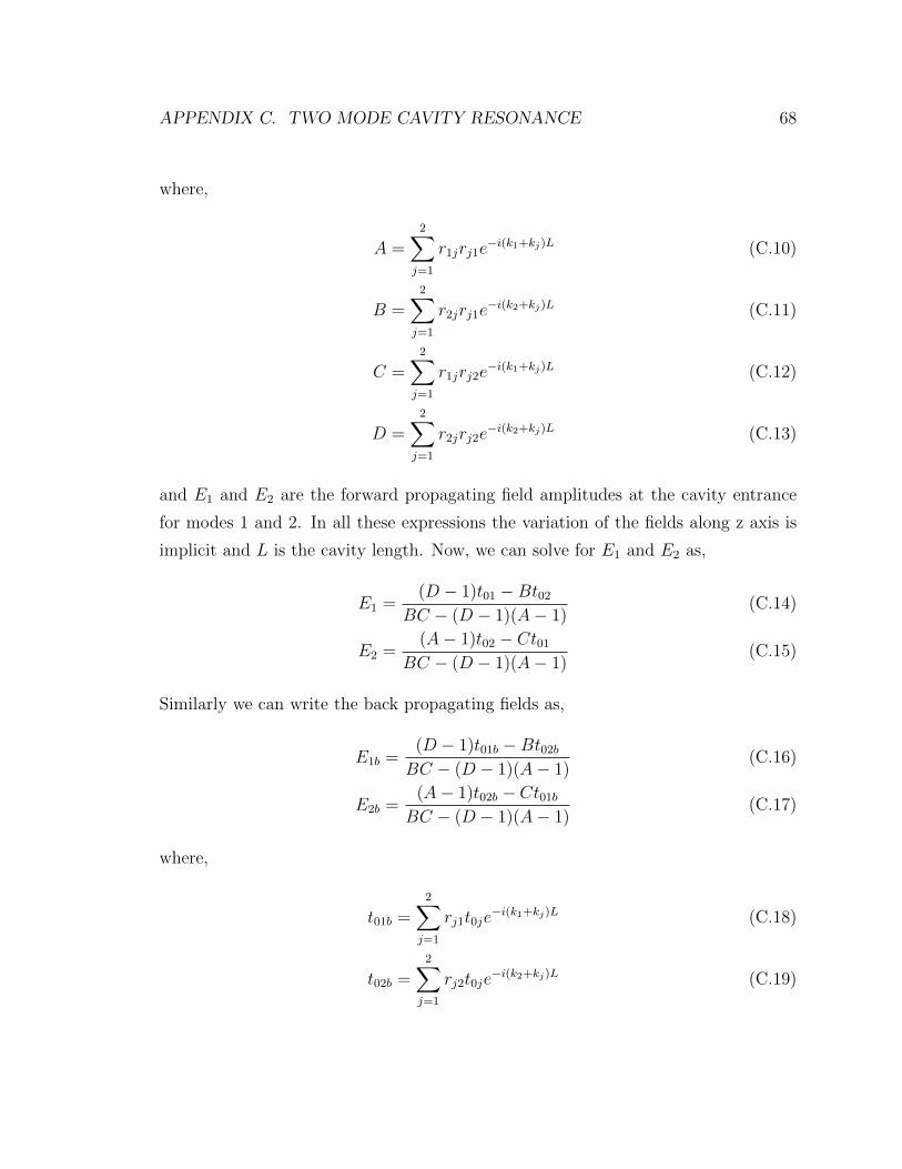
APPENDIX C. TWO MODE CAVITY RESONANCE 68
where,
A =2∑j=1
r1jrj1e−i(k1+kj)L (C.10)
B =2∑j=1
r2jrj1e−i(k2+kj)L (C.11)
C =2∑j=1
r1jrj2e−i(k1+kj)L (C.12)
D =2∑j=1
r2jrj2e−i(k2+kj)L (C.13)
and E1 and E2 are the forward propagating field amplitudes at the cavity entrance
for modes 1 and 2. In all these expressions the variation of the fields along z axis is
implicit and L is the cavity length. Now, we can solve for E1 and E2 as,
E1 =(D − 1)t01 −Bt02
BC − (D − 1)(A− 1)(C.14)
E2 =(A− 1)t02 − Ct01
BC − (D − 1)(A− 1)(C.15)
Similarly we can write the back propagating fields as,
E1b =(D − 1)t01b −Bt02bBC − (D − 1)(A− 1)
(C.16)
E2b =(A− 1)t02b − Ct01b
BC − (D − 1)(A− 1)(C.17)
where,
t01b =2∑j=1
rj1t0je−i(k1+kj)L (C.18)
t02b =2∑j=1
rj2t0je−i(k2+kj)L (C.19)

APPENDIX C. TWO MODE CAVITY RESONANCE 69
and Finally the reflection and transmission coefficients can be derived to be ,
t = E1t10e−ik1L + E2t20e
−ik2L (C.20)
r = r00 + E1bt10 + E2bt20 (C.21)
The calculated values for the reflection (R = |r|2) and transmission (T = |t|2)for different cavity lengths and the same quantities derived from full field FDFD
simulations is given in 3.12i. The excellent agreement between the two, even for very
small stripe widths, validate the coupled cavity model.

Bibliography
[1] Barnes, W. L.; Dereux, A.; Ebbesen, T. W. Surface plasmon subwavelength
optics. Nature 2003, 424, 824–830.
[2] Maier, S. Plasmonics: Fundamentals and Applications; Springer: 2007.
[3] Economou, E. Surface plasmons in thin films. Physical Review 1969, 182, 539.
[4] Maier, S. Effective Mode Volume of Nanoscale Plasmon Cavities. 2006, 38,
257-267.
[5] Min, B.; Ostby, E.; Sorger, V.; Ulin-Avila, E.; Yang, L.; Zhang, X.; Va-
hala, K. High-Q surface-plasmon-polariton whispering-gallery microcavity. Na-
ture 2009, 457, 455–458.
[6] Gong, Y.; Vuckovic, J. Design of plasmon cavities for solid-state cavity quantum
electrodynamics applications. Applied Physics Letters 2007, 90, 033113-1-3.
[7] Yokota, H.; Saito, K.; Yanagida, T. Single molecule imaging of fluorescently
labeled proteins on metal by surface plasmons in aqueous solution. Physical
Review Letters 1998, 80, 4606-9.
[8] Pettinger, B.; Ren, B.; Picardi, G.; Schuster, R.; Ertl, G. Nanoscale probing of
adsorbed species by tip-enhanced Raman spectroscopy. Physical Review Letters
2004, 92, 096101.
[9] Pettinger, B.; Tadjeddine, A.; Kolb, D. Enhancement in raman intensity by
use of surface-plasmons. Chem. Phys. Lett. 1979, 66, 544-548.
70

BIBLIOGRAPHY 71
[10] Righini, M.; Volpe, G.; Girard, C.; Petrov, D.; Quidant, R. Surface plas-
mon optical tweezers: Tunable optical manipulation in the femtonewton range.
Physical Review Letters 2008, 100, 186804.
[11] Chen, C.; Osgood, R. Direct observation of the local-field-enhanced surface
photochemical-reactions. Physical Review Letters 1983, 50, 1705-1708.
[12] Cao, L.; Barsic, D. N.; Guichard, A. R.; Brongersma, M. L. Plasmon-Assisted
Local Temperature Control to Pattern Individual Semiconductor Nanowires and
Carbon Nanotubes. Nano Letters 2007, 7, 3523-3527.
[13] Jun, Y. C.; Pala, R.; Brongersma, M. L. Strong Modification of Quantum
Dot Spontaneous Emission via Gap Plasmon Coupling in Metal Nanoslits. The
Journal of Physical Chemistry C 2009, 7269-7273.
[14] Bakker, R. M.; Yuan, H.-K.; Liu, Z.; Drachev, V. P.; Kildishev, A. V.;
Shalaev, V. M.; Pedersen, R. H.; Gresillon, S.; Boltasseva, A. Enhanced lo-
calized fluorescence in plasmonic nanoantennae. Applied Physics Letters 2008,
92, 043101.
[15] Farahani, J. N.; Pohl, D. W.; Eisler, H.-J.; Hecht, B. Single Quantum Dot
Coupled to a Scanning Optical Antenna: A Tunable Superemitter. Phys. Rev.
Lett. 2005, 95, 017402.
[16] Taminiau, T. H.; Moerland, R. J.; Segerink, F. B.; Kuipers, L.; van
Hulst, N. F. Œ/4 Resonance of an Optical Monopole Antenna Probed by Single
Molecule Fluorescence. Nano Letters 2007, 7, 28-33.
[17] Cai, W.; White, J. S.; Brongersma, M. L. Compact, High-Speed and Power-
Efficient Electrooptic Plasmonic Modulators. Nano Letters 2009, 4403-4411.
[18] Nikolajsen, T.; Leosson, K.; Bozhevolnyi, S. I. Surface plasmon polariton based
modulators and switches operating at telecom wavelengths. Applied Physics
Letters 2004, 85, 5833-5835.

BIBLIOGRAPHY 72
[19] Krasavin, A. V.; Zheludev, N. I. Active plasmonics: Controlling signals in
Au/Ga waveguide using nanoscale structural transformations. Applied Physics
Letters 2004, 84, 1416-1418.
[20] Domenico Pacifici, Henri J. Lezec, H. A. A. All-optical modulation by plasmonic
excitation of CdSe quantum dots. Nature Photonics 2007, 1, 402-406.
[21] Hryciw, A.; Jun, Y. C.; Brongersma, M. L. Plasmonics: Electrifying plasmonics
on silicon. Nat Mater 2010, 9, 3–4.
[22] Walters, R. J.; van Loon, R. V. A.; Brunets, I.; Schmitz, J.; Polman, A. A
silicon-based electrical source of surface plasmon polaritons. Nat Mater 2010,
9, 21–25.
[23] Raether, H. Surface Plasmons; Springer Tracts in Modern Physics Springer:
1988.
[24] Weeber, J.-C.; Bouhelier, A.; Colas des Francs, G.; Markey, L.; Dereux, A.
Submicrometer In-Plane Integrated Surface Plasmon Cavities. Nano Letters
2007, 7, 1352-1359.
[25] Zia, R.; Selker, M. D.; Catrysse, P. B.; Brongersma, M. L. Geometries and
materials for subwavelength surface plasmon modes. Journal of the Optical So-
ciety of America A: Optics and Image Science, and Vision 2004, 21, 2442 –
2446.
[26] Zayats, A. V.; Smolyaninov, I. I.; Maradudin, A. A. Nano-optics of surface
plasmon polaritons.. Physics Reports 2005, 408, 131 – 314.
[27] Hofmann, C. E.; Vesseur, E. J. R.; Sweatlock, L. A.; Lezec, H. J.; Garcıa de
Abajo, F. J.; Polman, A.; Atwater, H. A. Plasmonic Modes of Annular Nanores-
onators Imaged by Spectrally Resolved Cathodoluminescence. Nano Letters
2007, 7, 3612-3617.
[28] Bharadwaj, P.; Bouhelier, A.; Novotny, L. Electrical Excitation of Surface
Plasmons. Phys. Rev. Lett. 2011, 106, 226802.

BIBLIOGRAPHY 73
[29] Sambles, J. R.; Bradbery, G. W.; Yang, F. Optical excitation of surface plas-
mons: An introduction. Contemporary Physics 1991, 32, 173-183.
[30] Dionne, J.; Sweatlock, L.; Atwater, H.; Polman, A. Planar metal plasmon
waveguides: frequency-dependent dispersion, propagation, localization, and loss
beyond the free electron model. Physical Review B 2005, 72, 075405.
[31] Berini, P. Long-range surface plasmon polaritons. Adv. Opt. Photon. 2009, 1,
484–588.
[32] Ditlbacher, H.; Hohenau, A.; Wagner, D.; Kreibig, U.; Rogers, M.; Hofer, F.;
Aussenegg, F. R.; Krenn, J. R. Silver Nanowires as Surface Plasmon Res-
onators. Phys. Rev. Lett. 2005, 95, 257403.
[33] Takahara, J.; Yamagishi, S.; Taki, H.; Morimoto, A.; Kobayashi, T. Guiding
of a one-dimensional optical beam with nanometer diameter. Opt. Lett. 1997,
22, 475–477.
[34] Novotny, L. Effective wavelength scaling for optical antennas. Physical Review
Letters 2007, 98, 1 – 4.
[35] Søndergaard, T.; Bozhevolnyi, S. I. Strip and gap plasmon polariton optical
resonators. physica status solidi (b) 2008, 245, 9–19.
[36] Miyazaki, H. T.; Kurokawa, Y. Controlled plasmon resonance in closed
metal/insulator/metal nanocavities. Appl. Phys. Lett. 2006, 89, 211126.
[37] Miyazaki, H.; Kurokawa, Y. Squeezing visible light waves into a 3-nm-thick
and 55-nm-long plasmon cavity. Physical Review Letters 2006, 96, 097401.
[38] White, J. S.; Veronis, G.; Yu, Z.; Barnard, E. S.; Chandran, A.; Fan, S.;
Brongersma, M. L. Extraordinary optical absorption through subwavelength
slits. Opt. Lett. 2009, 34, 686-688.
[39] Ishi, T.; Fujikata, J.; Marita, K.; Baba, T.; Ohashi, K. Si nano-photodiode
with a surface plasmon antenna. Jpn. J. Appl. Phys. 2005, 44, L364-L366.

BIBLIOGRAPHY 74
[40] Jun, Y. C.; Huang, K. C. Y.; Brongersma, M. L. Plasmonic beaming and
active control over fluorescent emission. Nat Commun 2011, 2, 1-4.
[41] Neutens, P.; Van Dorpe, P.; De Vlaminck, I.; Lagae, L.; Borghs, G. Electrical
detection of confined gap plasmons in metal-insulator-metal waveguides. Nat
Photon 2009, 3, 283–286.
[42] Bozhevolnyi, S. I.; Søndergaard, T. General properties of slow-plasmon resonant
nanostructures: nano-antennas and resonators. Opt. Express 2007, 15, 10869–
10877.
[43] Søndergaard, T.; Bozhevolnyi, S. Slow-plasmon resonant nanostructures: Scat-
tering and field enhancements. Phys. Rev. B 2007, 75, 073402.
[44] Bryant, G. W.; Garcia de Abajo, F. J.; Aizpurua, J. Mapping the Plasmon
Resonances of Metallic Nanoantennas. Nano Letters 2008, 8, 631–636.
[45] Sondergaard, T.; Beermann, J.; Boltasseva, A.; Bozhevolnyi, S. I. Slow-
plasmon resonant-nanostrip antennas: Analysis and demonstration. Physical
Review B 2008, 77, 115420.
[46] Barnard, E. S.; White, J. S.; Chandran, A.; Brongersma, M. L. Spectral
properties of plasmonic resonator antennas. Opt. Express 2008, 16, 16529–
16537.
[47] Ford, G. W.; Weber, W. H. Electromagnetic interactions of molecules with
metal surfaces. Phys. Rep. 1984, 113, 195–287.
[48] Barnes, W. L. Fluorescence near interfaces: The role of photonic mode density.
Journal of Modern Optics 1998, 45, 661-699.
[49] Novotny, L.; van Hulst, N. Antennas for light. Nat Photon 2011, 5, 83–90.
[50] Fromm, D. P.; Sundaramurthy, A.; Schuck, P. J.; Kino, G.; Moerner, W. E.
Gap-Dependent Optical Coupling of Single “Bowtie” Nanoantennas Resonant
in the Visible. Nano Letters 2004, 4, 957-961.

BIBLIOGRAPHY 75
[51] Jun, Y. C.; Kekatpure, R. D.; White, J. S.; Brongersma, M. L. Nonreso-
nant enhancement of spontaneous emission in metal-dielectric-metal plasmon
waveguide structures. Phys. Rev. B 2008, 78, 153111.
[52] Cai, W.; Vasudev, A. P.; Brongersma, M. L. Electrically Controlled Nonlinear
Generation of Light with Plasmonics. Science 2011, 333, 1720-1723.
[53] Bouhelier, A.; Beversluis, M.; Hartschuh, A.; Novotny, L. Near-Field Second-
Harmonic Generation Induced by Local Field Enhancement. Phys. Rev. Lett.
2003, 90, 013903.
[54] Lippitz, M.; van Dijk, M. A.; Orrit, M. Third-Harmonic Generation from
Single Gold Nanoparticles. Nano Letters 2005, 5, 799-802.
[55] Beversluis, M. R.; Bouhelier, A.; Novotny, L. Continuum generation from
single gold nanostructures through near-field mediated intraband transitions.
Phys. Rev. B 2003, 68, 115433.
[56] Jamid, H. A.; AlBader, S. J. Diffraction of surface plasmon-polaritons in an
abruptly terminated dielectric-metal interface. IEEE Photonics Technology Let-
ters 1995, 7, 321 – 3.
[57] Leskova, T.; Gapotchenko, N. Fabry-Perot type interferometer for surface-
polaritons - resonance effects. Solid State Comm. 1985, 53, 351-357.
[58] Leskova, T.; Maradudin, A.; Zierau, W. Surface plasmon polariton propagation
near an index step. Opt. Comm. 2005, 249, 23-35.
[59] Zia, R.; Chandran, A.; Brongersma, M. L. Dielectric waveguide model for
guided surface polaritons. Opt. Lett. 2005, 30, 1473 – 1475.
[60] Gordon, R. Light in a subwavelength slit in a metal: Propagation and reflec-
tion. Physical Review B (Condensed Matter and Materials Physics) 2006, 73,
153405.

BIBLIOGRAPHY 76
[61] Porto, J.; Garcia-Vidal, F.; Pendry, J. Transmission resonances on metallic
gratings with very narrow slits. Physical Review Letters 1999, 83, 2845-2848.
[62] Szentirmay, Z. Slow-mode surface plasma oscillations in layered structures.
Physical Review B 1987, 36, 2607–13.
[63] Bozhevolnyi, S. I., Ed.; Plasmonic Nanoguides and Circuits; Pan Stanford:
2009.
[64] Sukru Ekin Kocabas,; Veronis, G.; Miller, D. A. B.; Fan, S. Modal analysis
and coupling in metal-insulator-metal waveguides. Physical Review B 2009, 79,
035120.
[65] Hernandez, G. Fabry-Perot Interferometers; Oxford Oxfordshire: Oxford Uni-
versity Press: 1986.
[66] Takakura, Y. Optical Resonance in a Narrow Slit in a Thick Metallic Screen.
Physical Review Letters 2001, 86, 5601–5603.
[67] Jackson, J. D. Classical electrodynamics; 3rd ed.; Wiley: New York, NY, 1999.
[68] Lalanne, P.; Hugonin, J.; Rodier, J. Theory of surface plasmon generation at
nanoslit apertures. Physical Review Letters 2005, 95, 263902.
[69] Fan, S. Surface Plasmon Nanophotonics. In ; Mark L. Brongersma,; Kik, P. G.,
Eds.; Springer Series in Optical Sciences Springer: 2007; Chapter 12, pages
169–182.
[70] Rakic, A.; Djurisic, A.; Elazar, J.; Majewski, M. Optical properties of metallic
films for vertical-cavity optoelectronic devices. Appl. Opt. 1998, 37,.
[71] Esteban, R.; Teperik, T. V.; Greffet, J. J. Optical Patch Antennas for Single
Photon Emission Using Surface Plasmon Resonances. Phys. Rev. Lett. 2010,
104, 026802.
BIBLIOGRAPHY 77
[72] Sun, S.; Yang, K.-Y.; Wang, C.-M.; Juan, T.-K.; Chen, W. T.; Liao, C. Y.;
He, Q.; Xiao, S.; Kung, W.-T.; Guo, G.-Y.; Zhou, L.; Tsai, D. P. High-
Efficiency Broadband Anomalous Reflection by Gradient Meta-Surfaces. Nano
Letters 2012, 12, 6223-6229.
[73] Pors, A.; Albrektsen, O.; Radko, I. P.; Bozhevolnyi, S. I. Gap plasmon-based
metasurfaces for total control of reflected light. Sci. Rep. 2013, 3, 1-6.
[74] Liu, Y.; Palomba, S.; Park, Y.; Zentgraf, T.; Yin, X.; Zhang, X. Com-
pact Magnetic Antennas for Directional Excitation of Surface Plasmons. Nano
Letters 2012, 12, 4853-4858.
[75] Kriesch, A.; Burgos, S. P.; Ploss, D.; Pfeifer, H.; Atwater, H. A.; Peschel, U.
Functional Plasmonic Nanocircuits with Low Insertion and Propagation Losses.
Nano Letters 2013, 13, 4539-4545.
[76] Kosako, T.; Kadoya, Y.; Hofmann, H. F. Directional control of light by a
nano-optical Yagi-Uda antenna. Nat Photon 2010, 4, 312–315.
[77] Pakizeh, T.; Kall, M. Unidirectional Ultracompact Optical Nanoantennas.
Nano Letters 2009, 9, 2343-2349.
[78] Weeber, J. C. Near-field observation of surface plasmon polariton propagation
on thin metal stripes. Phys. Rev. B 2001, 64, 045411.
[79] Zia, R.; Selker, M. D.; Brongersma, M. L. Leaky and bound modes of surface
plasmon waveguides.. Physical Review B 2005, 71, 165431 – 1.
[80] Berini, P.; Charbonneau, R.; Lahoud, N. Long-Range Surface Plasmons on
Ultrathin Membranes. Nano Letters 2007, 7, 1376-1380.
[81] Bozhevolnyi, S. I.; Volkov, V. S.; Devaux, E.; Laluet, J.-Y.; Ebbesen, T. W.
Channel plasmon subwavelength waveguide components including interferome-
ters and ring resonators. Nature 2006, 440, 508–511.
BIBLIOGRAPHY 78
[82] Dionne, J. A.; Sweatlock, L. A.; Atwater, H. A.; Polman, A. Plasmon slot
waveguides: Towards chip-scale propagation with subwavelength-scale localiza-
tion. Phys. Rev. B 2006, 73, 035407.
[83] Bozhevolnyi, S. I.; Volkov, V. S.; Devaux, E.; Ebbesen, T. W. Channel
plasmon-polariton guiding by subwavelength metal grooves. Phys. Rev. Lett.
2005, 95, 046802.
[84] Koller, D. M. Organic plasmon-emitting diode. Nature Photon. 2008, 2, 684–
687.
[85] Nie, S.; Emory, S. R. Probing Single Molecules and Single Nanoparticles by
Surface-Enhanced Raman Scattering. Science 1997, 275, 1102-1106.
[86] Lezec, H. J.; Degiron, A.; Devaux, E.; Linke, R. A.; Martin-Moreno, L.;
Garcia-Vidal, F. J.; Ebbesen, T. W. Beaming Light from a Subwavelength
Aperture. Science 2002, 297, 820-822.
[87] Schuck, P. J.; Fromm, D. P.; Sundaramurthy, A.; Kino, G. S.; Moerner, W. E.
Improving the Mismatch between Light and Nanoscale Objects with Gold
Bowtie Nanoantennas. Phys. Rev. Lett. 2005, 94, 017402.
[88] Bharadwaj, P.; Deutsch, B.; Novotny, L. Optical Antennas. Adv. Opt. Photon.
2009, 1, 438–483.
[89] Barnard, E. S.; White, J. S.; Chandran, A.; Brongersma, M. L. Spectral
properties of plasmonic resonator antennas. Opt. Express 2008, 16, 16529–
16537.
[90] Anemogiannis, E.; Glytsis, E. N.; Gaylord, T. Determination of guided and
leaky modes in lossless and lossy planar multilayer optical waveguides: reflection
pole method and wavevector density method. Lightwave Technology, Journal of
1999, 17, 929-941.

BIBLIOGRAPHY 79
[91] Rakic, A. D.; Djurisic, A. B.; Elazar, J. M.; Majewski, M. L. Optical Properties
of Metallic Films for Vertical-Cavity Optoelectronic Devices. Appl. Opt. 1998,
37, 5271–5283.
[92] Barnard, E. S.; Pala, R. A.; Brongersma, M. L. Photocurrent mapping of
near-field optical antenna resonances. Nat Nano 2011, 6, 588–593.
[93] Chandran, A.; Barnard, E. S.; White, J. S.; Brongersma, M. L. Metal-
dielectric-metal surface plasmon-polariton resonators. Phys. Rev. B 2012, 85,
085416.
[94] Okamoto, K.; Niki, I.; Scherer, A.; Narukawa, Y.; Mukai, T.; Kawakami, Y.
Surface plasmon enhanced spontaneous emission rate of InGaNGaN quantum
wells probed by time-resolved photoluminescence spectroscopy. Applied Physics
Letters 2005, 87, 71102-1-3.
[95] Wedge, S.; Wasey, J. A. E.; Barnes, W. L.; Sage, I. Coupled surface
plasmon-polariton mediated photoluminescencefrom a top-emitting organic
light-emitting structure. Applied Physics Letters 2004, 85, 182-184.
[96] Miller, D. A. B.; Chemla, D. S.; Damen, T. C.; Gossard, A. C.; Wiegmann, W.;
Wood, T. H.; Burrus, C. A. Band-Edge Electroabsorption in Quantum Well
Structures: The Quantum-Confined Stark Effect. Phys. Rev. Lett. 1984, 53,
2173–2176.
[97] Drozd, V.; Baraban, A.; Nikiforova, I. Electrical properties of Si—Al2O3
structures grown by ML-ALE. Applied Surface Science 1994, 82–83, 583 - 586.
[98] Empedocles, S. A.; Bawendi, M. G. Quantum-Confined Stark Effect in Single
CdSe Nanocrystallite Quantum Dots. Science 1997, 278, 2114-2117.
[99] Liu, J. S. Q.; White, J. S.; Fan, S.; Brongersma, M. L. Side-coupled cavity
model for surface plasmon-polariton transmission across a groove. Opt. Express
2009, 17, 17837–17848.

BIBLIOGRAPHY 80
[100] Lalanne, P.; Hugonin, J. P.; Rodier, J. C. Approximate model for surface-
plasmon generation at slit apertures. J. Opt. Soc. Am. A 2006, 23, 1608–1615.