MEMS STMicroelectronics reveals top-performing MEMS ... · LIS344AHH (Courtesy of...
16
LIS344AHH (Courtesy of STMicroelectronics) ISSUE N°149 24/09/2013 THE DISRUPTIVE SEMICONDUCTOR TECHNOLOGIES MAGAZINE Free registration on www.i-micronews.com PLATINUM PARTNERS: Everywhereyoulook ™ NANOTECHNOLOGY T he patent-pending LED creates a more precise wavelength of UV light than commercially available UV LEDs, and runs at much lower voltages and is more compact than other experimental methods for creating precise wavelength UV light. The LED could lend itself to applications for chemical detection, disinfection, and UV curing. With significant further development, it might someday be able to provide a source for UV lasers for eye surgery and computer chip manufacture. >p.13 New kind of ultraviolet LED based on nanowires could lead to portable, low-cost devices Commercial uses for ultraviolet (UV) light are growing, and now a new kind of LED under development at The Ohio State University could lead to more portable and low-cost uses of the technology. MEDTECH M icrofluidic devices move liquids through tiny, hair-sized pathways carved into glass slides and have distinct advantages over traditional laboratories when it comes to medical diagnostics. At these reduced scales, fluid transport is enhanced by factors such as diffusion and high surface-to- volume ratios, making testing procedures much faster. By constructing parallel arrays of microfluidic pathways, researchers are working to produce ‘lab-on-a-chip’ technologies that allow multiple biological tests to be performed using just a drop of blood or urine. In a development that promises to make lab-on-a-chip devices more portable and economic to construct, Yo Tanaka from the RIKEN Quantitative Biology Center and colleagues have now produced a new type of microfluidic control valve that takes up significantly less space on a microchip than existing approaches. >p.8 Lab-on-a-chip technology gets a flexible upgrade Electrically responsive polymers help make miniature systems for biomedical analysis even more compact. T he high bandwidth of the new device permits a high output data rate allowing sustained accurate measurement of rapidly changing accelerations, enabling enhanced industrial controls, robotic equipment and wearable electronics such as sports monitors. Combining high data rate with low-noise operation that enables monitoring of small- amplitude displacements, ST’s newest accelerometer delivers smoother, more responsive performance in motion-activated controls and also supports more demanding applications such as virtual augmented reality. >p.6 REVERSE COSTING 3 SORAA: GaN on GaN LED EQUIPMENT & MATERIALS 4 Polymer via-filling to improve reliability of 3D-IC / TSV packaging PHOTOVOLTAICS 12 Soitec launches new solar- energy module featuring 31.8% efficiency MEMS s kytron energy, based in Berlin, Germany, has focused on developing and manufacturing monitoring, control, and supervision solutions for renewable generation power plants since 1977. Back then, photovoltaics weren’t considered a viable solution for power generation at the utility-scale level… >p.3 skytron energy’s monitoring, control, and supervision system for photovoltaic applications skytron energy specializes in high-tech monitoring, control, and supervision solutions for photovoltaic power generation plants. Today, more than 4.5 gigawatts of installed solar capacity worldwide rely upon their instrumentation system. INSIDE… STMicroelectronics reveals top-performing MEMS accelerometer for richer user experiences STMicroelectronics’ latest high-performance 3-axis MEMS accelerometer, the LIS344AHH, enhances gaming, user-interface and augmented reality experiences, as well as industrial controls and impact monitoring, by providing a large full-scale range of up to ±18g combined with high bandwidth, low noise, and high mechanical and thermal stability. EDITORIAL The growth of advanced packaging I just returned this morning from another trip in Asia, this time in Malaysia where I had the opportunity to meet a large community of engineers involved and interested in learning more about latest developments in Advanced Packaging. The past month was quite a busy month in terms of events, from the ASTRI 3D Workshop In 3D Packaging, hold at Science Park in Hong Kong, to Semicon Taiwan in Taipei, EMPC in Grenoble and now the workshops in Malaysia organized by IEEE CPMT; additionally, several customers and R&D centers visits worldwide. A busy month but very exciting and rewarding. After 2 years of mostly focusing on front end of the line applications I am very glad to return to Advanced Packaging world by joining Yole Développement and see the enthusiasm, latest developments and the wide variety of activities happening here. I really missed that and glad to be back. Quite a lot going on in Advanced Packaging. It is very encouraging to observe the importance packaging has gained in the past years and the growth we further expect to see in this segment. By 2018, the forecasts performed by our very talented analysts here at Yole, shows a double annual growth rate (21%) of the total Wafer-Scale-Level IC packaged wafers compare to the growth of the total IC semiconductor wafers (CAGR 10% 2011-2017). If the penetration rate of the packaging industry is today approximately 17%, this growth will continue, expected to reach 23% by 2017. A lot of interest in 3D Packaging, including 3DIC, Interposer and Embedded Technologies (Fan- out and Embedded die). >p.2
Transcript of MEMS STMicroelectronics reveals top-performing MEMS ... · LIS344AHH (Courtesy of...

LIS344AHH (Courtesy of STMicroelectronics)
ISSUEN°149
24/09/2013
T H E D I S R U P T I V E S E M I C O N D U C T O R T E C H N O L O G I E S M A G A Z I N E
Free registration on www.i-micronews.com
P L A T I N U M P A R T N E R S :
Everywhereyoulook™
NANOTECHNOLOGY
The patent-pending LED creates a more precise wavelength of UV light than commercially available UV LEDs, and runs at much lower voltages and is more
compact than other experimental methods for creating precise wavelength UV light.The LED could lend itself to applications for chemical detection, disinfection, and UV curing. With signifi cant further development, it might someday be able to provide a source for UV lasers for eye surgery and computer chip manufacture.
>p.13
New kind of ultraviolet LED based on nanowires could lead to portable, low-cost devicesCommercial uses for ultraviolet (UV) light are growing, and now a new kind of LED under development at The Ohio State University could lead to more portable and low-cost uses of the technology.
MEDTECH
Microfl uidic devices move liquids through tiny, hair-sized pathways carved into glass slides and have distinct advantages over traditional laboratories when it comes
to medical diagnostics. At these reduced scales, fl uid transport is enhanced by factors such as diffusion and high surface-to-volume ratios, making testing procedures much faster. By constructing parallel arrays of microfluidic pathways, researchers are working to produce ‘lab-on-a-chip’ technologies that allow multiple biological tests to be performed using just a drop of blood or urine. In a development that promises to make lab-on-a-chip devices more portable and economic to construct, Yo Tanaka from the RIKEN Quantitative Biology Center and colleagues have now produced a new type of microfl uidic control valve that takes up signifi cantly less space on a microchip than existing approaches. >p.8
Lab-on-a-chip technology gets a fl exible upgradeElec tr ical ly responsive polymers help make miniature systems for biomedical analysis even more compact.
The high bandwidth of the new device permits a high output data rate allowing sustained accurate measurement of
rapidly changing accelerations, enabling enhanced industrial controls, robotic equipment and wearable electronics such as spor ts monitors. Combining high data rate with low-noise operation that enables monitoring of small-ampl i tude d i sp lacement s, ST ’s newes t acce lerometer del ivers smoother, more responsive performance in motion-activated controls and also supports more demanding applications such as virtual augmented reality.
>p.6
REVERSE COSTING 3
SORAA: GaN on GaN LED
EQUIPMENT & MATERIALS 4
Polymer via-fi lling to improve reliability of 3D-IC / TSV packaging
PHOTOVOLTAICS 12
Soitec launches new solar-energy module featuring 31.8% effi ciency
MEMS
skytron energy, based in Berlin, Germany, has focused on developing and manufac tur ing monitoring, control, and supervision solutions for
renewable generation power plants since 1977. Back then, photovoltaics weren’t considered a viable solution for power generation at the utility-scale level…
>p.3
skytron energy’s monitoring, control, and supervision system for photovoltaic applicationsskytron energy specializes in high-tech monitoring, control, and supervision solutions for photovoltaic power generation plants. Today, more than 4.5 gigawatts of installed solar capacity worldwide rely upon their instrumentation system.
INSIDE…
STMicroelectronics reveals top-per forming MEMS accelerometer for richer user experiencesSTMicroelectronics’ latest high-performance 3-axis MEMS accelerometer, the LIS344AHH, enhances gaming, user-interface and augmented reality experiences, as well as industrial controls and impact monitoring, by providing a large full-scale range of up to ±18g combined with high bandwidth, low noise, and high mechanical and thermal stability.
EDITORIAL
The growth
of advanced
packaging
I ju s t r e turned th i s morning from another trip in As ia, th is t ime in Malaysia where I had the opportunity to meet a large community of engineers involved and interested in learning more about latest developments in Advanced Packaging. The past month was quite a busy month in terms of events, from the ASTRI 3D Workshop In 3D Packaging, hold at Science Park in Hong Kong, to Semicon Taiwan in Taipei, EMPC in Grenoble and now the workshops in Malaysia organized by IEEE CPMT; additionally, several customers and R&D centers visits worldwide. A busy month but very exciting and rewarding. After 2 years of mostly focusing on front end of the line applications I am very glad to return to Advanced Packaging world by joining Yole Développement and see the enthusiasm, latest developments and the wide variety of activities happening here. I really missed that and glad to be back.
Quite a lot going on in Advanced Packaging. It is very encouraging to observe the importance packaging has gained in the past years and the growth we further expect to see in this segment. By 2018, the forecasts performed by our very talented analysts here at Yole, shows a double annual growth rate (21%) of the total Wafer-Scale-Level IC packaged wafers compare to the growth of the total IC semiconductor wafers (CAGR 10% 2011-2017). If the penetration rate of the packaging industry is today approximately 17%, this growth will continue, expected to reach 23% by 2017. A lot of interest in 3D Packaging, including 3DIC, Interposer and Embedded Technologies (Fan-out and Embedded die).
>p.2

2 | ISSUE N°149 | 24/09/2013
G O L D P A R T N E R S
About Yole DéveloppementFounded in 1998, Yole Développement has grown to become a group of companies providing marketing, technology and strategy consulting, media in addition to corporate fi nance services.With a strong focus on emerging applications using silicon and/or micro manufacturing, Yole Développement group has expanded to include more than 50 associates worldwide covering MEMS, Compound Semiconductors, LED, Image Sensors, Optoelectronics, Microfluidics & Medical, Photovoltaics, Advanced Packaging, Nanomaterials and Power Electronics. The group supports industrial companies, investors and R&D organizations worldwide to help them understand markets and follow technology trends to develop their business.
Consulting• Market data, market research & marketing analysis• Technology analysis• Reverse engineering & costing services• Strategy consulting• Patent analysisMore information on www.yole.fr
Reports• Collection of technology & market reports• Manufacturing cost simulation tools• Component reverse engineering & Costing
analysis• Patent investigation
Financial services• Mergers & Acquisitions• Due diligence & valuation• Fundraising• Coaching of emerging companies• IP portfolio management, valuation & optimizationMore information on www.yolefi nance.com
Media• Online disruptive technologies website: www.i-micronews.com• Editorial webcasts program• Six magazines: Micronews - MEMS Trends –
3D Packaging – iLED – Power Dev’• Communication & Webcasts services
ContactsFor more information about :• Consulting Services : Christophe Fitamant
(fi [email protected])• Financial Services: Géraldine Andrieux-Gustin
([email protected])• Reports: David Jourdan ([email protected])• Media & Communication : Sandrine Leroy
CONTENT
MEMS 6
MEDTECH 8
COMPOUND SEMICONDUCTORS 9
LED 10
IMAGING 11
OPTOELECTRONICS 11
PHOTOVOLTAICS 12
NANOTECHNOLOGY 13
ADVANCED PACKAGING 14
POWER ELECTRONICS 15
Editorial StaffBoard Members: Jean-Christophe Eloy - Media Activity, Editor in chief: Dr Eric Mounier - Editors: Jérôme Azémar, Frédéric Breussin, Thibault Buisson, Paul Danini, Wenbin Ding, Dr. Éric Mounier, Pars Mukish, Laurent Robin, Milan Rosina, Benjamin Roussel, Dr. Philippe Roussel - Media & Communication Manager: Sandrine Leroy - Media & Com-munication Coordinators: Clotilde Fabre, Camille Veyrier - Layout: atelier JBBOX - Production: Kzen
CONSULTING
EDITORIAL
The growth of advanced packaging
Let’s take 3DIC, for example: a couple of years ago when I was directly involved with 3DIC development and managing EMC3D consor t ium ac t iv i t ies, the number of organizations involved at that time with this technology were around 50. During a A recent IP analys is per formed by our c o l l e ague s f r om par tne r KnowMade d i s c ove r ed unve i l ed more than 260 organizations and 1700 inventors involved (in terms of IP) with ver t ical 3D stacking technologies (both 3D TSV and interposer). 1569 patents documents constituting 961 relevant patents were found, out of which 85% are active. Even though the fi rst patent
was found in 1969 (applied by IBM) and some activities in this area have taken place since then, most of the patents (82%) were applied after 2006 and today, almost half of the patents are still pending, showing the youth of this 3D IC technolog. If IBM and Micron were found to be the fi rst assignees, Hynix and StatsChipPac have emerged as new players during the past 5 years. Signifi cant number of patents were f illed by other companies, such as Samsung, TSMC, Intel, Amkor and, from the academia, ITRI is leading in terms of total number of patents, followed by CEA LETI, Fraunhofer, Kaist and IMEC.
High inte res t in a l l these packaging technologies and a real opportunity for the entire supply chain to work together and fur ther consolidate and strengthen the system value-chain in order to fully take advantage of the benefits and advantages these technologies can bring.
Rozalia Beica,
CTO and Business Unit Director, Advanced Packaging & Manufacturing, Yole Développement
From page 1
Developed by the pioneer of blue LED, Shuji Nakamura and fellow scientists at University of California, the first
GaN on GaN LEDs are today commercially available. With the GaN epitaxy on a GaN substrate, there are no dislocations, no strain, no piezoelectric fi elds in the multi quantum well with for result a very high brightness per mm².The 36 LEDs of 0.07 mm2 GaN-on-GaN revealed in tearing down Soraa’s MR16 lamps give an equivalent 50W halogen light.
Technology analysisPackaged in an original and clever housing in silicon, the SORAA LED integrates three phosphors, blue, green/yellow, red. The LED
emits in violet to obtain a broader color spec trum. The GaN epitaxy on a GaN substrate eliminates the need of a buffer layer with consequently a very thin epitaxy layer. The good GaN conduction allows a vertical structure for the LED, very simple to manufacture.
Costing resultsWith a manufacturing realized on 2-inch GaN wafers, the substrate cost is the main part of the cost, around 60%. The silicon package called Lightchip represents 20%. The full reverse costing report combining technological analysis of the devices and detailed manufacturing cost is already available.
24/09/2013 | ISSUE N°149 | 3
skytron energy’s monitoring, control, and supervision system for photovoltaic applicationsFrom page 1
INSIDE…
Today, it’s an entirely different story, which is refl ected by the more than 4.5 gigawatts of installed solar capacity
wor ldwide re ly ing on the company ’s monitoring components, all of which are developed and manufactured in Germany.
“We have about 100 employees, most of them assigned to the development of software and hardware applications for our mon i t o r i ng s o l u t i o n ,” s ay s Mon i k a Hennessen, key accounts manager for solar applications at skytron energy.
Controlling the entire power generation plantskytron energy operates its own control room in Berlin and can supervise their customers’ power generation plants all over the world. In fact, they frequently provide complete operations and maintenance services for their customers.
“Our goal has always been to cover the entire plant—from the point of power generation in the solar fi eld up to the grid connection point,” explains Hennessen. “We call our system a ‘fully integrated monitoring control and supervision system,’ because it provides real-time condition monitoring of all function groups in the power plant and can communicate with virtually all solar inverters in the market.”
High-precision measurement equipment is one of the key advantages skytron energy provides. The data collected in the plant serves as the information basis for remote plant supervision in the control room, and also provides details about the plant ’s performance.
“A powerful visualization system in the control room enables remote inspection of every single component in the plant,” says
Hennessen. Every measurement value logged in the plant can be zoomed in on and examined in high resolution in charts and graphs at the high-resolution of 1-minute mean values. This makes fault diagnosis and systematic service and maintenance work effi cient and cost effective.”Another feature of the system is the power plant controller, which is highly adaptable to local grid connection regulations—it’s not restricted specifi cally to the German grid.Utility-scale photovoltaic installations are fully-fledged power stations. This means they are industrial objects with extremely high demands on reliability and safety and a long service life of 25 to 30 years out in the fi eld.
Real-time monitoring protects investmentsThe prevailing business models of renewable power generation projects are investments, pr imarily rewarded by special feed-in tariffs—at least in most European countries. Or they’re based on special power purchase agreements.
Investors in these plants have a keen interest in producing as much energy as technically possible. “Any diminution in energy yield cuts their return on investment,
so any f laws in the plant that aren’ t remedied instantly can turn into painful fi nancial losses for the investor,” explains Hennessen. Without a proper real-time monitoring system, a failure or the underperformance of just a few solar panels is dif f icult to detect. “With high-precision monitoring in place, you can spot when something goes wrong in the plant and do the necessary repair work as quick ly as poss ib le,” Hennessen notes.
Other applicationsskytron energy’s instrumentation system is also fi nding use in other renewable energy applications such as wind and hybrid power plants. Hybrid installations typically use solar panels, often combined with wind power,
batteries for energy storage, and diesel generators as emergency backup. “These installations are usually much smaller than a solar power plant, typically below 1 megawatt. They’re much quicker to develop and build and not as complicated to fi nance. Their pr ime f ie lds of appl icat ion are currently in African and South American countries,” says Hennessen.
Their key characteristics lie in the fact that different forms of power generation are integrated into one plant. The installation must be capable of deciding which kind of energy source to use at a specifi c moment—whether it’s wind, solar, battery, or diesel gene ra to r. “S ince th i s needs t o be automatically controlled, we’re seeing a new f ie ld for our moni tor ing and contro l equipment,” Hennessen notes.
Future goalsskytron energy strives to expand its presence and venture out into new geographic markets, especially into the U.S, South America, South Africa and Eastern Europe, but also into Asian countries. The company is deeply committed to knowledge transfer and offers full-scale training programs to ensure that local staff will be able to take over and run their own plant’s operations and maintenance within 1 to 3 years.
“From a technology point of view, we are also opening up our system. Although it was originally designed for photovoltaics only, we are expanding it to cover other types of renewable power generation. We strive to offer an open- architecture system that can be used in photovoltaics, wind, and hybrid installations,” Hennessen says.
www.skytron-energy.com
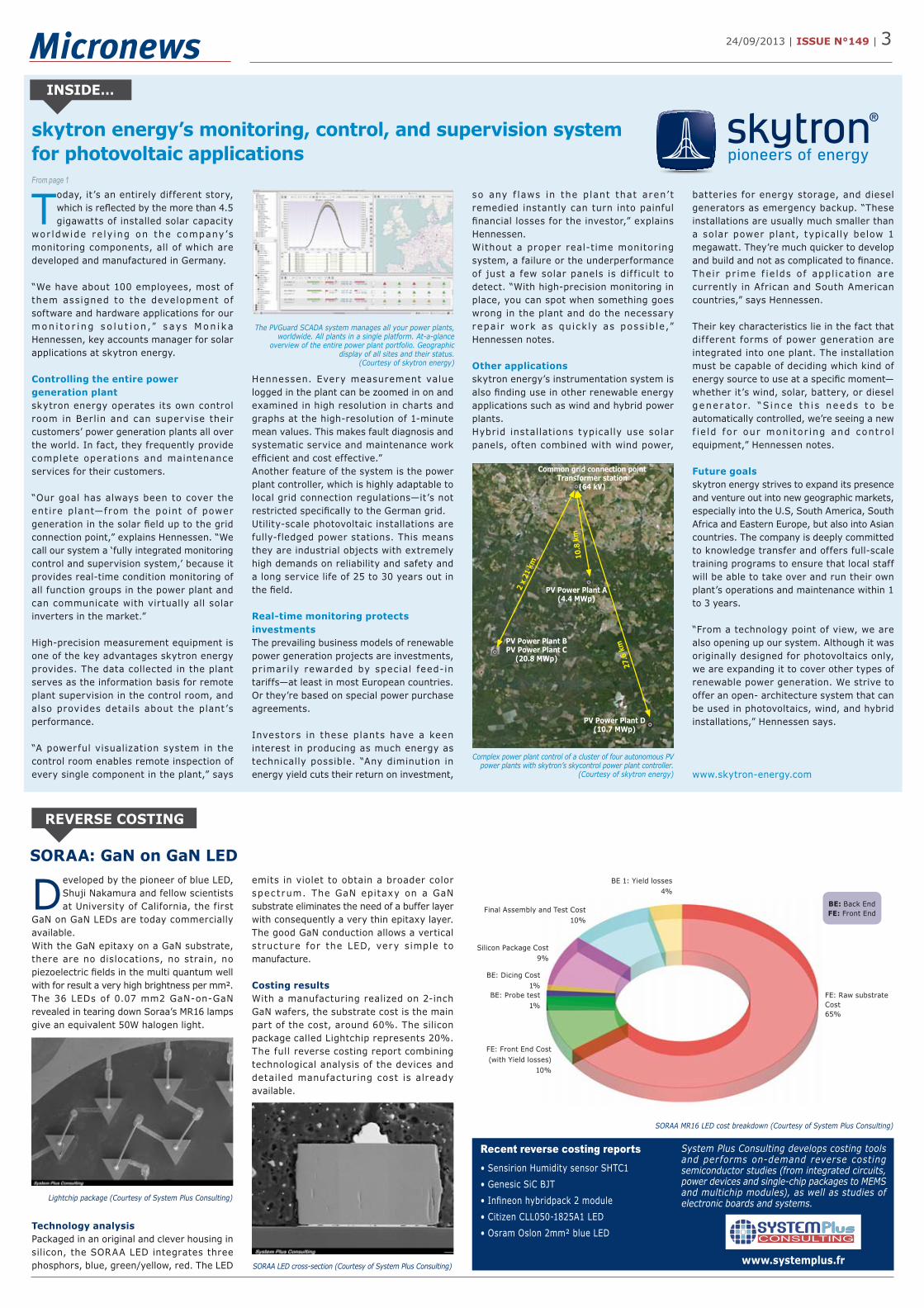
Complex power plant control of a cluster of four autonomous PV power plants with skytron’s skycontrol power plant controller.
(Courtesy of skytron energy)
The PVGuard SCADA system manages all your power plants, worldwide. All plants in a single platform. At-a-glance
overview of the entire power plant portfolio. Geographic display of all sites and their status.
(Courtesy of skytron energy)
REVERSE COSTING
SORAA: GaN on GaN LED
CONSULTING
Recent reverse costing reports• Sensirion Humidity sensor SHTC1
• Genesic SiC BJT
• Infi neon hybridpack 2 module
• Citizen CLL050-1825A1 LED
• Osram Oslon 2mm² blue LED
System Plus Consulting develops costing tools and performs on-demand reverse costing semiconductor studies (from integrated circuits, power devices and single-chip packages to MEMS and multichip modules), as well as studies of electronic boards and systems.
www.systemplus.fr
SORAA MR16 LED cost breakdown (Courtesy of System Plus Consulting)
Lightchip package (Courtesy of System Plus Consulting)
SORAA LED cross-section (Courtesy of System Plus Consulting)
Common grid connection pointTransformer station
(64 kV)
PV Power Plant A(4.4 MWp)
2 x
21 k
m
PV Power Plant BPV Power Plant C
(20.8 MWp)
PV Power Plant D(10.7 MWp)
10.8
km
27.6
km
FE: Raw substrate Cost65%
FE: Front End Cost (with Yield losses)
10%
BE: Probe test1%
BE: Dicing Cost1%
Silicon Package Cost9%
Final Assembly and Test Cost10%
BE 1: Yield losses4%
BE: Back EndFE: Front End

4 | ISSUE N°149 | 24/09/2013
EQUIPMENT & MATERIALS
Polymer via-fi lling to improve reliability of 3D-IC / TSV packagingThe successful progression of three-dimensional (3-D) integration on multi-level chip designs has enabled the evolution of smaller, faster and smarter devices.
Consumer demand for multifunctional electronic gadgets with reduced form f a c t o r h a s t h e r e f o r e g r e a t l y
stimulated 3-D integration for the past several years. A key driver for 3-D device i n t e g r a t i o n s c hemes ha s been t he realization of through-chip communication between multiple vertically stacked layers using through-silicon via (TSV) technology. The fabrication of TSVs, however, is not trivial and involves a series of processes mainly concerning wafer thinning, deep reactive ion etching, dielectric deposition, and electroplating of the actual through-via metal interconnection. Currently, mostly so l id Copper (Cu) v ia s t ruc tures are employed in TSV interconnects. Originally, the decision to use solid Cu fillings was motivated by the ease of Cu processing as well as the ability to keep manufacturing costs low by utilizing existing tooling infrastructure. However, as 3D fabrication technology has matured, the focus is moving toward the mitigation of reliability issues. The long term reliability of a TSV with so l id Cu f i l l ing is mainly compromised by the intrinsic mismatch of the coeffi cient of thermal expansion (CTE) b e t we e n t h e s o l i d Cu v i a an d t h e surrounding s i l icon substrate. Stress analysis during thermal cycling has shown very high stress concentration, especially in the vicinity of the corner portions. This mechanical stress within the via can cause the Cu filling to pop out of the via cavity, thereby put t ing the TSV connec t ion permanently out of function.
One approach to solve this issue is to replace solid fi lled Cu vias with alternative conducting media. However, this approach is undesirable because existing process technology and tool inf ras truc ture for Cu is a lready wel l established. A more promising solution points to a design change where the solid via fi lling is replaced by a partially plated through-via interconnect. For this approach, the internal via surface is lined with a conformal Cu layer, while the remaining void within the via is fi lled with a polymer. This new type of TSV interconnect design is more forgiving on CTE induced stress between the silicon substrate and the interfacing metal. The use of polymer materials as dielectric fi lling in deep silicon vias has been shown to improve the reliability of TSV interconnects by sealing the metal from atmospheric infl uences and preventing corrosion of the connection. Polymers also prov ide an add i t iona l advantage by planarizing the substrate’s top surface. For photosensitive polymers, the top portion also may serve as resist film for lithographic redistribution layer (RDL) formation.
Taking these benefi ts into account, this new TSV design is a very promising approach to fabricating ver tical interconnects with enhanced reliability and increased lifetime. The idea for such an advanced via design is not new; however, the spin- and spray-coating methods previously used for fi lling the high-aspect-rat io voids af ter TSV metallization have not been able to meet the required quality. Although both fabrication methods are well-established processes for polymer deposition, several disadvantages are associated with either method.
For example, when the spray-coating method is applied for via-fi lling, multiple coating cycles are required, which increase p r o c e s s i n g t ime and r e s u l t i n l ow
throughput. Moreover, the spray-coating process is typically limited to the use of low-viscosity liquid media. The mechanicals of the spin-coating method intrinsically cause trapping of air pockets under the deposited polymer layer within the vias. This trapped air expands during thermal cycling and can cause the polymer capping to bur s t . Ad jus t ing the r heo log i c a l proper t ies of the polymer in order to achieve the necessary fl ow into the cavities provides only limited success and can result in a par tially uncoated top sur face or strongly undulating surface topography on the wafer. Because of these limitations, there is a clear need for a method that allows void-free fi lling of deep wells with polymeric material. In addition, a good su r f a c e f l a t ne s s i s c r i t i c a l f o r any subsequent processing steps.
EV Group has developed a proprietary NanoFill process that utilizes innovative process technology for via f i l l ing and simultaneously forms a smooth polymeric interface on the wafer, while maintaining the high throughput rate necessary for the production line. Available on the EVG100 series of resist processing systems (see Figure 2), the NanoFill process furthermore allows the use of many different polymers with various desirable material properties to fi ll structures for a range of applications and purposes.
The transition of 3D-IC integration into volume production is driving the need to revisit existing manufacturing methods and develop new ones while attempting to cause as little disruption in the ecosystem as possible. One important area that is being addressed is TSV via filling, where a new approach has been developed that leverages existing toolsets and processes.
www.evgroup.com
Figure 1: The picture shows the void-free fi lling of vias without any voids (trapped air) within the polymer material – which often is the issue with alternative techniques. The picture also shows the consistency of doing this with multiple adjacent vias,
as well as the planarity of the polymer coating achieved atop the actual vias at the wafer’s surface (Courtesy of EV Group)
Figure 2: EVG®150 automated resist processing system (Courtesy of EV Group)
Save the date. Join us.
January 20-22, 2014Grenoble (France)
European 3D TSV SummitApplication Ready
The Power of [Integration]
www.semi.org/european3DTSVSummitContact: Yann Guillou ([email protected])
The must-attend event focusing on 3D TSV and gathering the full supply chain. In 2013, the 1st edition reached 97% satisfaction rate and had more than 320 attendees from 20 countries.
European 3D TSV Summit 2014 features:25 presentationsPanel discussions & Market session
ExhibitionPre-Summit SymposiumOne on one business meetingCEA-LETI 300mm TSV line tourCocktail Dinner

EUROPEAN PROJECT
COWIN supports startup Frec|n|sys COWIN is a support action, funded by the European Commission, dedicated to support the commercial exploitation of EU projects. One of the objective is to help technology startups not only launch, but to survive and thrive in Europe.
One of the startups COWIN has been assisting is Frec|n|sys, a company founded by Sylvain Bal landras.
Frec|n|sys is based on a technology that involves surface acoustic waves components suitable for high operating temperatures. The research effort was supported by the FP7 in the frame of the “SAW-HOT” Project. COWIN includes f ive partners, acting in supporting roles to help the startups, with Yole Développement acting as the lead facilitator. The group analyzed more than 200 projects from the European Commission and identifi ed “Golden Nuggets,” which they believed they could help accelerate from a technology to a product.Ballandras’ technology was identifi ed as one of these “Golden Nuggets” and was selected for COWIN support, in part, because “he had the ambition to create his own company based on his own expertise with surface acoust ic wave sensor s,” notes Regis Hamelin, senior technical manager for Euripides, which is also a partner of the COWIN support action.
Frec|n|sys’ SAW-HOT technologyFrec|n|sys’ SAW-HOT is a planar technology that involves depositing platinum electrodes on top of piezoelectric wafers.One of the goals of the project was to investigate the capabilities of the material used by Frec|n|sys, which is a single crystal comprised of a lattice of atoms combining lanthanum, gall ium, and si l icon oxide (La3Ga5SiO14). The material’s symmetry is very similar to quar tz. But contrary to quar tz, which experiences a change in symmetry when it reaches 573°C, this material’s symmetry doesn’t change. “This means that if you can deposit platinum electrodes on top of the material to excite waves, you will be able to do it at temperatures in excess of 573°C,” says Ballandras. “As part of our project, we were challenged to meet fi rst 650°C, then 900°C. Depositing the electrodes creates the conditions needed for launching waves on the surface of the wafer. These acoustic waves are propagated and guided by the surface, operated at 50MHz to 3GHz.”T hank s t o t he l i nea r p r ope r t i e s o f piezoelectricity, the electrodes are charged, which creates desirable conditions for launching the wave, which then becomes trapped at the surface of the device. So when the interrogation ends, the device must consume this trapped energy. “The best way to consume this trapped energy is to counter polarize the electrodes and the antenna, which re-emits the electromagnetic wave at the same frequency or resonant frequency of the device,” says Ballandras. “By monitoring the frequency, it’s possible to identify the temperature to which the device was subjected.”
In terms of survival of the sensor, he was able to demonstrate it at 740°C for 40 hours, and at 800°C for at least 4 hours—meaning the Frec|n|sys sensor (size: 1 cm2, with a thickness of 4mm) can be used in extremely harsh environments. The sensor was also tested for cryogenic conditions and performed well.
COWIN support of Frec|n|sysCOWIN is supporting Sylvain Ballandras in the validation of the company’s business plan and in business development with customers’ acquisition.
COWIN is acting to accelerate the growth of the company. Wi th COWIN suppor t , Bal landras entered a French nat ional competition for innovative startups, was s e l e c t ed among hundr eds o f o t he r contestants, and was awarded a prize supporting the launch of the company.“This prize makes it much easier to develop the company,” says Ballandras. “COWIN
helped me improve my business plan, because as a sc ientist I wasn’t really focusing on how to promote and market Frec|n|sys. I’ve definitely benefited from COWIN’s help.”On October 10, 2013, in Brussels, Belgium, COWIN will host the Investment Place, a one-day event to feature the star tup companies it is working with—including
Frec|n|sys. This is an excellent opportunity for venture capital is ts and corporate investors to explore these startups and to know more about COWIN activities.
To read the complete article, please visit i-Micronews.com website.
www.cowin4u.eu
Sponsored by Hosted by
Teledyne DALSA announces MIDIS™, the MEMS Integrated Designfor Inertial Sensors platform. MIDIS™ is the new MEMS technology ideal for high volume / low cost inertial sensing applications.
MIDIS™ PLATFORM BREAKS THEONE-PROCESS-PER-PRODUCTMEMS PARADIGM
WEBCAST AVAILABLE TODAY
To view or review the webcast, please go to I-Micronews.comand access the Archived Webcast section.
24/09/2013 | ISSUE N°149 | 5
Driven by smartphones & microfl uidic applications, emerging MEMS will account for 10% of the value of the total MEMS business by 2018.
MEMS Devices Emerging MEMS 2013
Technology and market report
Discover all our reports on www.i-micronews.com
KEY FEATURES:
• Understanding of the new MEMS devices under development and players involved
• Market data on new MEMS developments
• Identifi cation of new MEMS companies• Technical, economical & market
challenges / competing solutions faced
Publication date : August 2013
http://fr.slideshare.net/Yole_Developpement?utm_are.net/Yole_Devenet/Y//Y/Yt/Yt/Yt/Yet/Yet/Yet/Yet/Ynet/Ynet/Ynet/Ynet/Ynet/Ynet/Ynet/net/netnetnetnenenenn ole_D___D_D_D_D_D_D_De_De_De_De_De_De_De_De_Dle_Dle_Dle_Dle_Dle_Dle_Dle_Dle_Dole_Dole_Dole_Dole_Dole Doleoleoleoleoleoleoleoleoleoleoleoleoleoleoleoleoleollloooollcampaign=profi letracking&utm_ng&utm_g&utmfi letrackin uuu&&&&&&&g&g&g&gggggggg uing&uletrackiing&ukikkkckckmedium=sssite&utm_source=ssslideviewurce=tm_so ======e=e=e=e=e=e=e=e=ce=ce=cececececececercercercrcrcrcrurururururuuuuuuuuuurcrooososososo_so_so_s_s_sm_sm_m_m_m_m_mmmmmtmm
http://www.youtube.com/channel/UCxcAmfnGJgYXZyoutube.com hannel/UCxcAmfnGJgYXhannel/UCxcAhannel/UCxcAhannel/UCxcAmfnGJgYXmfnGJgYXmfnGJgYXel/UC cAel/UCxcAel/UCxcAel/UCxcAmfnGJgYmfnGJgYmfnGJgYmfnGJgYnnel/UC cAnnel/UCxcAnnel/UCxcAnnel/UCxcAmfnGJgYmfnGJgYmfnGJgYmfnGJgYyoutube.com/cn46VFs6ozQ?feature=watchQ?feature=watchhhhhQ?feature=watc
https://twittitter. ole_Devcom/Yol https://plus. 147949532143/google.com/1gle.com/1/omm/1.com/1le.com/1m/1e.com.cocogle.comgle.comle.coomomg 096843081840968430about
http://www.linkedin.com/company/w.linkedin.com/compnked n.com/coyole-d-velopppemenement
hhttttttttttttttttttttttp:/p:/p:/p:/p /p:/p:/p:/://p:/p:/p:/p:/p:/p:/p:/pp:/p:/p:/p:/:p:p:p://:p /ww/ww/ww/wwww/ww/ww/ww/ww/ww/ww/wwwwwww/ww/ww/ww/ww/ww/ww/wwwwww/wwww/ww/ w.iww.iw.iw.iww.iww.w.iww iw.iw iw.iw.iw.iw.ww.ww.iww.iw ----mmiciciciciciiccciciccciciccciccronrronronronronronronronronronroronroronronronronronronronnronrronronronr ewsewsewsewsewswsewswsewsewsewsewewsewewsewsewsewswsewwssewss.coc.cococo.co.c.co.co.c.co.co.coco.co.cococoo.coccocom/mmmmmmmmmmmmmmmmmmmmemememememmemememmmmmememememmmms/rs/rs/rs/rs/s/rs/rs/rs/rs/rs/r/s/rs/rs/s/rs/rs/rs/rs//rs/rs/ss/r/rs epoepoepoepoepoepoepoepopoepoepoepoepoepoepoepoepoepoeepoepoepoppppopepportsrtsrtsrtsrtsrtsrtsrtsrtsrtsrtsrtsrtssrtsrtrtsrtrtsrtstsrrtt //////////////////

24/09/2013 | ISSUE N°149 | 6
MEMS
Witness motion-tracking platform maker Sixense Entertainment Inc. of Los Gatos, Calif., which will make
first deliveries of its second-generation motion-tracking plat form and system development kit (SDK) to Kickstar ter backers. The Sixense Tracking Embedded Module (STEM) - the company’s fi rst wireless motion-tracking platform - will launch as a Kickstarter project on Sept. 12.
The STEM system is a six-degrees-of-freedom absolute motion tracker using proprietary magnetic coils - instead of MEMS chips - housed in a small oblong module that original equipment manufacturers (OEMs) can embed in their own controllers.To read the complete article, please visit EETimes website.
www.eetimes.com
As millions of fall sports participants take to the fi eld to kick off the 2013 sports season, players in a wide range of
activities are wearing electronic head-impact monitoring patches (“xPatches”) developed by X2 Biosystems with advanced technology from STMicroelectronics.
In addition to surpassing the milestone of 5,000 xPatch sensor systems shipped, the X2 Biosystems’ Integrated Concussion Exam (ICE) sof tware has been adopted by a broader audience. This customer list includes the NFL (National Football League), which has mandated the use of the X2 ICE in all practices and games of all 32 teams this season. A cloud-connected mobile application environment, the X2 ICE captures athlete concussion history and pre-season neuro-cognitive function, balance, and coordinate-performance data, which is then used as a baseline for comparison after a suspected injury event.
The X2 xPatch uses miniature sensors to monitor the impacts experienced by each player and transmits data to X2’s ICE software where sideline staff can examine it in context of the individual athlete’s recent impact history and lifetime concussion history.
X2 Biosystems worked with STMicroelectronics to build the wearable xPatches, which are smaller than an American Quarter (25-cent piece). They incorporate ST’s tiny MEMS motion-sensing chips, ultra low-power STM32L microcontroller, SPIRIT1 low-power radio transmitter, and miniature power-supply and battery-charging ICs.
“The development of the X2 Biosystems xPatch would not have been possible without ST’s advanced technologies. The xPatch integrates all required functions for head-impact monitoring, analysis, and wireless data transmission in a small, inconspicuous, comfortably wearable format,” said Christoph Mack, CEO of X2 Biosystems. “Because it’s so small and lightweight, it can be attached easily and unobtrusively behind the player’s ear - athletes forget they’re wearing it within minutes. This frees the athlete to perform at the limit of their abilities; playing hard, while playing safe.”“We are delighted that our technologies, including MEMS precision movement sensing and ultra low-power radio and ICs, have enabled the creation of the X2 xPatch system, augmenting spor ts bodies’ ef for ts to safeguard the wellbeing of participants,” commented Benedetto Vigna, Executive V ice President and General Manager,
A na l o g , MEMS and Senso r s G r oup, S T M i c r o e l e c t r o n i c s . “ T h e l e ve l o f miniaturization, integration, and power efficiency ST has been able to deliver has allowed X2 to apply its systems at the professional, university, high-school and youth levels in Football, Soccer, Hockey, Lacrosse, Boxing and Field Hockey. Through capturing and analyzing over 600,000 head impact events so far, X2 and ST are helping to keep athletes safer.”
Medical professionals within sports, military, and industrial safety areas believe that better management of concussions can help prevent serious brain injuries, which are associated with conditions such as dementia and depression later in life. The evidence is strong that the brain can repair itself after most concussions, if the condition is recognized and managed appropriately. Information provided by the X2 Concussion Management System helps to monitor impact events, promote adherence to the standard of care, coordinate the return to play process, and improve both acute and long-term brain health outcomes.
www.st.com
Sixense kickstarts wireless controllersEven established companies are starting to use Kickstarter.
STMicroelectronics and X2 Biosystems celebrate shipment of 5,000th concussion sensor systemAdvanced sensing, computing, RF and power chips in action in an unprecedented range of activities, from youth sports to the NFL.
www.plastic-electronics.org
Co-located with:
The Power of [x]
Emerging use-cases which are driving new MEMS technologies
Viable production concepts for MEMS products
The Power of [MEMS]
International MEMS/MST Industry Forum
www.semiconeuropa.org
8–10 October Messe Dresden, Germany
New materials and processes for MEMS, front-end, back-end and testing
Entering a New Growth Cycle!
EUVLED/SSL450mm
More than Moore
3D ICMEMS
Fab AutomationEquipment
Conference Sessions:
PF788FLF3
xPatch sensor system.(Courtesy of STMicroelectronics and X2 Biosystems)
The LIS344AHH full-scale range is user-se lec tab le up to ±6g or ±18g, enhancing performance over similar
devices that measure up to ±16g. The device has a supply voltage range of 2.4V to 3.6V, features embedded self-test, and is
housed in a compact 4mm x 4mm x 1.5mm 16-lead LGA-16 package.Engineering samples of the LIS344AHH are available now and budgetary unit pricing is $8.40 for orders over 1,000 pieces.www.st.com
STMicroelectronics reveals top-performing MEMS accelerometer for richer user experiencesFrom page 1
ZOOM
From a $2.2B business in 2012 to $6.4B by 2018!
MEMS for MobileMEMS for Cell
Phones and Tablets
Technology and market report
Discover all our reports on www.i-micronews.com
KEY FEATURES:
• Status of MEMS devices for cell phone applications
• 2010-2018 market forecasts and 2012 market shares
• Analysis of sensor fusion developments, including connected devices’ impact
Publication date : June 2013
http://fr.slideshare.net/Yole_Developpement?utm_p://fr.slideshare.nr.sliddlidlidslidslislisli.sli.slir.slr.slr.slr.sr.slr.slr.sl eshaahahahahahahahashashashashshshshshshshheshesheshesheshesheshesessheshesheshscampaign=profi letracking&utm_mpaign=profi letretratrampa gn=p=n=n=pn=pn=pn=pn=pgn=pgn=pgn=gn=gn=gn=gn=gngngngngngn profi lfi fi ofi ofi lofi lofi lofi lofi lofi lofi lofi lofi lofi lrofi lrofi lrofi lrofilrofilrofirofirofirofirofirofirofirofirofirofirofirororoproproproproproproprompamedium=sssite&utm_source=ssslideviewsite&utit &ium=ss &&&&&&&&&&&&e&e&e&e&e&&etetetetttititititiiisisss e&sssite&itesssssssssss=s=s=s=s==m=m=m=m=mmm
http://www.youtube.com/channel/UCxcAmfnGJgYXZwww.youtub com/channel/UCxcAm/com/ccom/ch l/UC Ahannel/UCxcAhannel/UCxcAmm//c/ch l/UC Ahannel/UCxcAhannel/UCxcAmmm/channel/UCxcAmwww ywww.youtubeoutube.n46VFs6ozQ?feature=6ozQ?featu = he=watche=watchatchatchhwatchwatchwatchs6ozQ?fs6ozQ?featureeature
https://twtwitter. m/Yole_Devcom httptps://plusssplululus//pluspluspplulus//pplplu////pl . 109684308147949532143/google.comgogoogle.comgoogle.com/1ogle.comgoogooggoogoogaboout
nkedin.com/company/tp://www.linhttp://www.ole-d-velopyo e-d-velop ementpe
htttp:/p:/p:/p:/p:/p:/p:/p:/p:/p:/p://p:/:/p:/p:/p:/p:p:/pp://p:/:p:p: /ww/ww/ww/ww/ww/ww/ww/ww/ww/ww/ww/ww/wwww/www/ww/ww/ww/ww/ww/ww/www/wwwww/wwww.iw.iw.iw.iw.iw.iw.iwww.iw iw.iw.iw.iw.iw.iwww.iww.w -------micronews.com/micccccccccccccccccccronronronronronronronronronronronronronrronronronrronroronronronronronronno ewsewsewsewsewsewsewsewsewsewsewsewsewsewsewswsewsewsewsswsewsewwew .co.co.coco.co.co.co.co.coco.co.co.coco.cococo.c.coc..co.coom/mmmmmmmmmmmmmmmmmmmmmmmememmmmmmemmemmmmmmemmmmmmms/rs/rs/rs/rs/rs/rs/rs/rs/rs/rs/rs/rs/rs/rs/rs/rs/rs/r/rss/rs/r/s//r/ epoepoepoepoepoepoepoepoepoepoepoepoepoepoepopoepoepoepooepoepoepopoppepep rtsrtsrtsrtstrtsrtsrtsrtsrtsrtsrtrtsrtrtsrrtsrtstrtsrtsrtstrtr ////////////////////

7 | ISSUE N°149 | 24/09/2013
MEMS
SAVE THE DATE
NOVEMBER 4-6, 2013Sonoma, CA, USA
PLATINUM SPONSORS
enjoy exclusive plenary sessions; hours of one-on-one meeting opportunities, plus a variety of social activities.
Mark your calendar, and help shape the future of inertial devices.
For more information, please contact S.Leroy ([email protected]) or visit www.memsinmotion.com
“I am extremely pleased with MEMS in Motion. It was great and I am looking forward to next year’s summit!” Vincent Fortin, Teledyne DALSA MEMS in Motion 2012 Participant “Some conferences you have just speakers and listeners, presentation afterpresentation. Forums like MEMS in Motion force interaction between peoplewhich tend to be more productive meetings. I would recommend this event to other industry people—100 percent.” Tom Flynn, Coventor MEMS in Motion 2012 Participant
High-performance inertial MEMS has been one of Tronics key businesses for about 15 years. The Company is
knowledgeable in all aspects of the sensor products f rom MEMS design to MEMS manufacturing, through ASIC integration, packaging, test and calibration. It has recently passed the meaningful mark of one million high-performance sensors delivered. These produc ts were pr imar i ly high-p e r f o r m a n c e a c c e l e r o m e t e r s a n d gyroscopes.
Designing and manufacturing such products requires know-how that is signif icantly di f ferent f rom that needed for lower performance products, such as consumer accelerometers and gyroscopes.
The key technologies that have allowed Tronics’ success in this fi eld are the use of
thick SOI, well-controlled high-aspect ratio DRIE, as well as high vacuum and low stress packaging. In addition to the principal technological elements, manufacturing high-performance inertial MEMS requires solid experience in the following challenging activit ies: keeping t ight control of all process steps with the abil ity to fully understand the failure modes down to the root causes, achieving good yields with a relatively low number of wafers processed, ensur ing 100% individual component traceability on all tests performed, gathering signifi cant reliability and stability data, and mastering the use of high performance characterization tools.
One million units delivered is a signifi cant milestone, not only because the typical sales price is somewhere between several tens of dollars to several hundreds of
dollars, but also because in these markets, the volumes are typically thousands per year rather than millions per year.
Stéphane Renard, founder of Tronics said: “16 years after founding the company, it is very satisfying for me to see our millionth high performance inertial sensor delivered, and I want to thank our longtime customers for their trust”.
Tronics has been serving several markets where high-performance inertial MEMS are either well established or gaining ground. Some examples are oil exploration, medical devices, aeronautical instrumentation, and vehicle control.
There is signifi cant growth in these markets as MEMS performance is challenging some of the older, more expensive technologies,
especially for the gyroscope. Tronics’ strength resides in its ability to design and manufac ture customer-spec i f ic high-per formance iner t ial MEMS relat ively quickly, thanks to its broad knowledge base. Tronics intends to remain a key player in the field of custom high-performance inertial MEMS design and manufacturing.
Tronics announced that it has appointed industry veteran Pascal Langlois as Chief Executive Offi cer. He will succeed Pe te r P f luge r, who r e t i r ed a f te r successfully leading the company for the past 10 years.
www.tronicsgroup.com
Cast in i t s quar tz-micro-e lec tro-me c han i c a l s y s t em (Q -MEMS) process, Epson contends that the
V340’s low drift - seven degrees per hour - gives it bias instability that rivals much larger IMUs.
“Q-MEMS’s advantage is that its makes possible a form factor like the V340 - about the size of a Chicklet - and yet this IMU achieves the same level of performance as much larger units,” said David Gaber, product marketing manager for IMUs, in an interview with EE Times. The new V340 IMU is 90 percent smaller than its predecessor
and is aimed at high-precision iner tial sensing applications such as navigation in unmanned systems, down-hole drilling, medical equipment, and aerospace.
To read the complete article, please visit EETimes website.
www.eetimes.com
Tronics delivered its millionth high performance inertial MEMS sensorAfter 15 years in the business, Tronics has sold more than one million high performance inertial MEMS sensors. A significant number in markets where yearly volumes are typically in the thousands.
Q-MEMS downsizes inertial measurement unitsLaying claim to the world’s smallest high-precision inertial measurement unit (IMU) Epson Electronics America, of San Jose, Calif., unveiled its six-degrees-of-freedom (DoF) combo accelerometer / gyroscope chip, which measures a scant 12x10x4 millimeters.
Net
wor
king
DaySEMI MEMS
Tech SeminarBringing MEMS science to the heart of MEMS industrial success
26 September 2013 Castelletto (Italy) - www.semi.org/euHosted by STMicroelectronics
This Tech Seminar is a SEMI Europe initiative to support European companies, start ups and laboratories involved in the growing MEMS market.
The Tech Seminar will feature:
Organized by:
Contact: [email protected]
KeynotesInvited talks from executives & technical expertsSpeed Networking sessionsNetworking Dinner on Sept 25th
Sponsored by:
Hosted by:
The onslaught of next generation t e c h n o l o g i e s c o m i n g t o t h e semiconductor industry will bring
demand for a host of new materials, but also an increasingly fragmented materials market, making strategic investment decisions for materials development even more risky and complex than usual.
As the semiconductor industry transitions to EUV lithography, new memory and logic architectures, 3D packaging, and 450mm wafers, adjacent markets from MEMS to f lexible electronics also demand new materials of their own. Navigating all these
oppor tuni t ie s wi l l r equire rea l i s t i c judgments of market potential and timing, b u t n ew app r o a c he s — i n c l u d i ng fundamental materials modeling, more efficient screening methods, and better industry collaboration — could also be key to easing profi table development. Higher-resolution, higher-speed inspection and metrology tools will also be vital to move these new materials into volume production.
To read the complete article, please visit SEMI website.
www.semi.org
Looming IC industry changes mean proliferation of new materials needs By Paula Doe, SEMI Emerging markets.

8 | ISSUE N°149 | 24/09/2013
In the majority of microfluidic devices, silicone pneumatic valves are used to manipulate liquid samples. Pneumatic
valves, however, require noisy compressors and complicated air channel systems, which are often too bulky for practical lab-on-a-chip applications. Piezoelectr ic actuators—inorganic crystals that change shape when e lec t r i ca l ly s t imulated—are feas ib le alternatives, but while piezoelectric materials are less obtrusive than pressurized air technology, they are excessively large when compared to the size of the microchip itself.Tanaka and his colleagues instead investigated the remarkable properties of electroactive polymers. These materials are rubber-like organic compounds that expand and contract when exposed to an electric current. As electroactive polymers can exhibit large mechanical strain force at small scales, the team deduced that creating membranes incorporating these materials could be a promising way to miniaturize microfluidic control valves.After experimenting with many valve shapes, the researchers settled on a micrometer-sized, dome-shaped polymer diaphragm sandwiched between soft electrode sheets. They tested its
ability to stop fl ow by fabricating it on top of a small hole drilled into a microfl uidic channel. By monitoring fl uorescent polystyrene tracking beads using high-speed video cameras, the team saw that stimulating the electroactive polymer caused the diaphragm to expand and close off the microchannel at sub-second speeds, nearly identical to the response time of piezoelectric actuators but with an order-of-magnitude smaller form factor. Furthermore, the polymer structure strongly resisted leaks because of its resilient structure.
The researchers note that the improved size-scaling of their valve system should prove more effi cient for the sorting of biological cells
than current fl uorescent technology. Other—more mobile—applications also may be on the horizon. “Many portable devices for personal diagnosis, environmental analysis, or fuel cells
could benefi t from these miniaturized valves,” says Tanaka.
www.rikenresearch.riken.jp
Lab-on-a-chip technology gets a fl exible upgradeFrom page 1
Sony DADC develops smart consumables for Quanterix Simoa HD-1 analyzer The Simoa Disc is the first diagnostic developed using Sony DADC’s optical disc manufacturing technology; will be used in Simoa technology to improve testing quality in life science research.
MEDTECH
A novel electroactive polymer stop valve for lab-on-a–chip technology (Courtesy of RIKEN Quantitative Biology Center)
Quanterix Corporation announced that the Simoa HD-1 Analyzer recently launched by Quanterix uses a “Smart
Consumable” designed and manufactured by Sony DADC BioSciences called the Simoa Disc.
For use in life science research and in vitro diagnostics (IVD) markets in the future, the Simoa disc is used to achieve higher levels of sensitivity and precision and is the first d iagnos t ic consumable whose assay technology is based on optical disc formats by Sony DADC. Prior to commercializing
Simoa, Quanterix needed a high-performance optics consumable that met the requirements of high sensitivity diagnostic testing and lent itself to high volume manufacturing processes at a low cost.
Through its relationship with Sony DADC, Quanterix was able to develop a strategy to performing single-molecule isolation and detection in micro arrays of microwells in a low-cost polymeric device confi guration. The Quanterix Simoa disc leverages established high-volume polymer replication based on opt ica l d isc technology for low cos t
manufacturing of disposable single molecule arrays. The Simoa technology is now commercially available and empowering life science researchers to explore biomarkers and pathways with greater sensitivity and precision, fueling the development of new diagnostic tests and improved treatment of diseases in oncology, neurology, cardiology, and other fi elds of medicine.
www.sonydadc.com
Off (valve open)
On (valve closed)
Flow
Elastomer WireGlass Soft electrodeAcrylic resin Electroactive polymer
Flow
FlowFlow
Researchers at MIT have found a way to detect early-stage malarial infection of blood cells by measuring changes in
the infected cells’ electrical properties. The scientists, from the laboratories of MIT’s Anantha Chandrakasan and Subra Suresh have built an experimental microfluidic device that takes a drop of blood and streams it across an elec trode that measures a signal differentiating infected cells from uninfected cells. The work is a first step toward a field-ready, low-cost, portable malaria-detection device. “Ultimately the goal would be to create a postage stamp-sized device with integrated electronics that can detect if a person has ma la r i a and a t what s t age ,” s ays Chandrakasan, the Joseph F. and Nancy P. Keithley Professor of Electrical Engineering and a pr incipal investigator at MIT’s Microsystems Technology Laboratories (MTL), who specializes in developing low-
power e l e c t r on i c dev i c e s . S im i l a r diagnostics may be applicable to other infections and diseases.To read the complete article, please visit i-Micronews.com website
www-mtl.mit.edu
Detecting early-stage malarial infection New prototype device recognizes electrical properties of infected cells as signatures of disease.
ZOOM
Sungjae Ha and Anantha Chandrakasan demonstrate the chip (Courtesy of MIT)
SIMOA Microfl uidic chips (Courtesy of Simoa)
How are NGS technologies revolutionizing the way
we think about healthcare?
Next Generation Sequencing
Next Generation Sequencing (NGS) : Market & Technology
Analysis
Technology and market report
Discover all our reports on www.i-micronews.com
KEY FEATURES:
• 2013-2018 NGS equipment and consumable market
• Sequencing technologies and cartridges associated
• Detailed supply chain and business model analysis
• Company profi les of the main players
Publication date : August 2013
http://fr.slideshare.net/Yole_Developpement?utm_/fr.slideshare.neslidededededeideidelidlidlidslidslidslidslidslidslidslidslid sharereareareareareareararararharharharharharharharharharharhashashashashashahahahahahhhahahahahcampaign=profi letracking&utm_aign=profiletractrackracpaign=prpp=pr=pr=pr=pr=pr=pr=pr=pn=pn=pn=pn=pn=pn=n=n=n ofi letlelelefilefilefilefilefiletfi letfiletfiletfiletfiletfiletfilefilefilefileofileofileofileofileofileofilofilofilofilofilofiofiofiofiofiofiofiofifififipaigmedium=sssite&utm_source=ssslideviewte&utmt &um=sssi uuuuuuuuu&u&u&u&u&u&u&u&u&u&u&&&&&e&e&eeeeeeetetett &usite&ue&sisisisisssssssssssssssssss=s=s=s=s==m=
http://www.youtube.com/channel/UCxcAmfnGJgYXZww.youtube. om/channel/UCxcAmf//om/com/ch l/UC Ah l/UC Ahannel/UCxcAhannel/UCxcA ffmfmfcch l/UC Ahannel/UCxcAhannel/UCxcAmcchannel/UCxcAhannel/UCxcAmmww yww yww.youtube cooutube cooutube.con46VFs6ozQ?feature=wozQ?feature w=watch=watchwatcchchtchtchtchtch6ozQ?f6ozQ?feature=eature=
https://twiwitter. m/Yole_Devcom/ httpss://plus/plusus/pluslus/plusluspluspluspl/plusus.. 09684308147949532143/google.com/1google.comgoogle.comoglegle.comgoogleooogleoooo le 0abouut
edin.com/company/http://www.linkehttp /www.linyole-d-veloole d-velop mentpemp
htttp:/p:/p:/p:/p:/p:/p:/p:/p:/p:/p://p:/p:/p:/p /ww/ww/ww/ww/ww/ww/ww/wwww/ww/ww/ww/ww/wwwww/wwww/wwwwww.iw.iw.iw.iw.iw.iw.iw.iw.iiw.iw.iw.iw.iw.iw.iw.w.i--------mimicccccccccronronronronronronronronronronronronononrononrononewsewsewsewsewsewsewswewsewsewsewewsewswsewsewsws.......coommmmmmmmmmmmmmmm/me/me/me/me/me/me/me/me/me/me/mm/me/me/me/me/me/m/medtedtedtedtedtedtedtedtedtedtedtedtedtedtedtedtedtedtet ch/ch/ch/ch/chch/ch/ch/ch/ch/ch/ch/ch/ch/ch/ch/ch/ch/ccrepportortortortortortrtortortortorortoro ts/s/s/s/s/s/s/s/s/s/s/s/s//s/s//s/s/

9 | ISSUE N°149 | 24/09/2013
COMPOUND SEMICONDUCTORS
According to them, the innovation could open the door to a new generation of LED technology that is less expensive
to manufacture, signifi cantly more effi cient, and which enables new functionalities and applications far beyond illumination.Presently, LED lighting systems are chips made from GaN, a semiconductor material. For the LED to function, many external components—such as inductors, capacitors, silicon interconnects and wires—must be installed on or integrated into the chip. The
large size of the chip, with all of these necessary components, complicates the design and performance of LED lighting products. Addit ionally, the process of assembling these complex LED lighting systems can be slow, manually intensive and expensive.In a study led by T. Paul Chow, professor in the department of electrical, computer, and systems engineering at Rensselaer, the researchers sought to solve this challenge by developing a chip with components all made
from GaN. This type of monolithically integrated chip s impli f ies LED device manufacturing, with fewer assembly steps and less required automation. Additionally, LED devices made with monolithically integrated chips will have fewer parts to malfunction, higher energy efficiency and cost effectiveness, and greater lighting design fl exibility.Chow and the research team grew a GaN LED structure directly on top of a GaN high-electron-mobility transistor (HEMT) structure.
They used several basic techniques to interconnect the two regions, creating what they are calling the fi rst monolithic integration of a HEMT and an LED on the same GaN-based chip.
To read the complete article, please visit EETAsia website.
www.eetasia.com
Peregrine Semiconductor announced the signing of a collaborative agreement with Murata Manufacturing Company on
a multi-sourcing arrangement for RF switches based on Peregrine’s proprietary UltraCMOS®
techno logy. Under the co l laborat ion agreement, Murata agrees to source a majority of its RF switching requirements from Peregrine in exchange for being granted a license to purchase or manufacture RF CMOS swi tches ut i l i z ing Peregr ine ’s technology and intellectual property (IP). The parties expect this agreement to result in an
expanded source of supply for these critical RF components and to assure global OEMs broad access to RF CMOS products.Peregrine Semiconductor pioneered RF CMOS-based devices with its UltraCMOS®
technology, an advanced form of silicon-on-insulator (SOI) process, and more than 20 years of research and development have resulted in 150 patents issued and pending. With this strong IP portfolio, Peregrine has established a leading position in the RF front-end section of mobile devices for RF switches and tunable RF components.
Murata is a leading supplier of RF front-end (RFFE) modules for the global mobile wireless marketplace. RF front-end modules are products that incorporate RF switches and tuning devices with SAW filters, passive components, and advanced packaging techniques. “Global OEM customers of both Peregrine and Murata have for some time requested that the companies implement an independent source of supply for the critical switching elements that are widely utilized in smart phones and other wireless-communications products,” said Jim Cable, Peregrine’s president and
CEO. “This agreement marks the fi rst license of Peregrine’s switch-based intellectual property to a third party.”Regarding announcement, Norio Nakajima, Murata’s Vice President, Communication Business Unit, stated, “Peregr ine has fundamental IP in CMOS-based switches and tun ing produc t s wi th i t s U l t raCMOS technology. This IP licensing arrangement solidifi es our existing relationship and future collaboration with Peregrine.
www.psemi.com
RF Micro Devices int roduced the RFHA1027, a GaN matched power transistor (MPT) that will deliver
industry-leading pulse power performance of 500W in a compact fl anged package at L-Band.RFMD’s new amplifi er is optimized for pulsed power applications requiring effi ciency and compact size. It operates from 1.2 GHz to 1.4 GHz and provides 500W of pulsed RF power from a 50 Volt supply. It also offers high gain of 16.5 dB and high effi ciency of 55 percent. The RFHA1027 is housed in a small form factor package of 24mm by 17.4 mm, and is input and output matched to 50 ohms, effi ciently minimizing external components. In addition, the package leverages RFMD’s advanced heat-sink and power-dissipation technologies to deliver excellent thermal stability and conductivity.The RFHA1027 targets new and existing radar architectures requiring ruggedness and reliability. The introduction of RFHA1027 follows the previous release of RFHA1020 (280W L-Band) and RF3928 (280W S-Band). To read the complete article, please visit i-Micronews.com website
www.rfmd.com
GT Advanced Technologies introduced its new SiClone™100 silicon carbide (S iC) p roduc t ion f urnace. The
SiClone100 uses a sublimation growth technique capable of producing high quality semiconducting bulk SiC crystal that can be fi nished into wafers up to 100 millimeters in diameter. In its initial offering, the SiClone100 is targeted at customers that have developed their own hot zone, qualifi ed a bulk crystal production recipe and are looking to begin volume production. “GT’s new SiClone100 furnace addresses the need in the power
electronics industry for more high quality SiC material for use in advanced, high power, high frequency devices,” said Tom Gutierrez, GT’s president and CEO. “The SiClone100 lays the foundation for our SiC product roadmap that is expected over time to provide customers with access to a complete production environment including recipes, hot zones and consumables capable of producing up to eight-inch SiC wafers.” GT has leveraged its deep domain expertise in crystal growth technology to of fer customers who are looking to move from “the lab to the fab” a
highly reliable and proven platform to begin volume production of SiC bulk crystal. The SiClone100 furnace is equipped with a state-of-the-art control system, which helps to automate the growth process by integrating the furnace electronics into the human-machine inter face (HMI) control. The SiClone100 uses a bottom loading design making it easy to load the hot zone. The control system provides increased fl exibility for users to customize process recipes and control key production parameters such as temperature, profile, ramp and gas flow,
wh i c h impr ove s r un- t o - r un c on t r o l r epeat ab i l i t y thus he lp ing to l ower manufacturing costs. GT’s onsite engineering and support help customers quickly ramp to volume production.The company continues to expect SiC furnace sales to contribute to less than 1% of its calendar year 2013 revenue and expects the SiC revenue ramp in 2014 and beyond to develop at a gradual pace given the lengthy design cycle associated with new power devices.b1www.gtat.com
GT Advanced Technologies introduces silicon carbide furnace New product line targets growth opportunities in power electronics market.
Research combines LED, power transistor in GaN chip A team of researchers from the Smart Lighting Engineering Research Centre at Rensselaer Polytechnic Institute has integrated an LED and a power transistor on a single GaN chip.
Peregrine Semiconductor completes collaborative sourcing and UltraCMOS® license agreement with Murata License covers advanced RFSOI- based design, process and third-party sourcing.
RFMD introduces 500 Watt GaN L-band amplifi er RFHA1027 supports radar architectures requiring ruggedness and reliability.
Get the 25+ key slides of the report…
NEW OFFER:The Executive Summary A concise analysis and main conclusions to make formal decision.
Executive Summary
Discover all our reports on www.i-micronews.com
Advantages of the executive summary:
• Quick overview of the domain
• Key information selected by the expert
• Special price : 2.490€
http://fr.slideshare.net/Yole_Developpement?utm_share.net/Yole_Dere.netetnetnetnetnene.ne.nee.nee.nee.nee.nere.nere.nre.nre.nre.nre.ne nee.ne.ne n /YoleeleleleleoleoleoleoleoleoleYoleYoleYoleYoleYoleYoleYoleYoleYoleYoleYolYolYol/Yol/Yol/Yol/Yol/Yol/Yol/Yo/Yo/Yo/Yo/Yo/Yo/Yo/YoYoYoYY/Yo/YoYoYoYcampaign=profi letracking&utm_rofiletracking&utm&utm&utmprofi letetracaacacracracracractractractratratratraetretretrttt king&g&g&g&g&ng&ng&ng&ng&ng&ng&ng&ng&ng&ng&ngngngngingingingingingininininininkikikikikikikikikkkrofi lmedium=sssite&utm_source=ssslideview_source=e&utm_ ccccrcrcrcrcrcrcrcururururururururuououooooooososossssourm_soursou__m_m_m_m_m_mmmmtmtmtmutmutmututuu&u
http://www.youtube.com/channel/UCxcAmfnGJgYXZw.youtube.co /channel/UCxcAmfnGJg/c/channel/UCxcAhannel/UCxcAmfnGJgmfnGJggl/UC Annel/UCxcAnnel/UCxcA f GmfnGmfnGannel/UCxcAannel/UCxcAmfnGmfnGmfnGww.y t bt boutube.comn46VFs6ozQ?feature=watzQ?feature=w t hatchatchatchzQ?fzQ?feature=weature=w
https://twitwitter. Yole_Devcom/Yo https://pluus. 08147949532143/google.com/1gle.comgle.le.cle coe.come.com/1coe oe.e.e.c mm 096843080968430968430 684about
http://www.linkedin.com/company/ww.linkedin.com/colinkedin.com/yole-d-veelopp ementpement
hhtttttttttttttttttttttttttttttttttttttp://p:/p:/p:/p:/p:p:/p://p:/p:/p:/pp:/pp:p:pp:p:/p:/p:/p:/p:/p://p:/p:p:/p:p://p:/pp /ww/ww/ww/w/ww/ww/ww/ww/ww/ww/ww/ww/wwwwww/ww/ww/ww/ww/wwww/wwww/ww/ww/www/wwwwwwwwwwww/wwwww/ww/w/wwwwww/wwww.iw.iw.iw iw.ww.w.iw.iw.w.iw.w.iw.iw.iww.w iw.iw.iiw.iwww.iw iw.iwwww.wwww.iw. -----------micronews.com/micicmiciccicicicmicimicmicicicicmicicmicccciicccmicicmicicccmimicmicicicccicronrorononronronronronronronronronronoronronrononnronnronnronronrooronnnrronronroroonnronnronnronewsewewsewswsewsewwsewsewsewewewwsewsewsewewsewsewewsewsewsewssewwsswseewswswswwwewwwwsswewe .co.coco.co.cocoo.ccocococococoo.cococococococo.co.coccocococooccoococoommm/mmmmmmmmmmmmmmmmmmmmmmmmmmmmmmmrrepepeppppppepepeppppppppepepppepeppppppportortortorortortorortortortrtortortortrtorortortrtortorortoortoooortortooro tooooooo ttts/s/s/s/s/s/s/s/s/s/s/s/s/s/s/ss/ss/ss//s/ssss/ss/ss/

24/09/2013 | ISSUE N°149 | 10
LED
Quantum Materials establishes milestone as fi rst company to deliver Tetrapod Quantum Dot samples to LCD display manufacturerQuantum Materials announced it has shipped Tetrapod Quantum Dots in sample quantities to a diversified leading Asian-based electronics manufacturer.
LG Innotek mass produces 6-inch wafer-based UV LED LG Innotek has overcome limits of the previous UV LED products by applying to the 6-inch wafer a vertical LED chip technology the Company developed on its own to enhance productivity and optical power of UV LED.
Cree introduces industry’s fi rst $99 LED street light as a direct replacement for residential street lights Cree announced an industry-changing technology breakthrough for the LED street lighting market.
Tetrapod Quantum Dots are an advanced nanoscale material that improves the performance and energy efficiency of
very high-resolution computer, TV and smartphone displays. Quantum Materials’ patent-pending continuous-fl ow technology produces uniform, narrow bandwidth tetrapod quantum dots with bright emission, less aggregation, purer colors (including high-
luminous red) and precise color rendition. Manufacturers are seeking to “print” tetrapod quantum dots onto backplane fi lms in liquid crystal displays (LCD) for brighter images, larger screens and a wider gamut of colors to deliver a new visual experience in image technology. Thinner, lighter, brighter and less expensive QD-LED displays, including portable and fl exible devices, will offer almost infi nite
contrast levels, deep black levels and high light output with no motion blur or field-of-view issues. Stephen Squires, Quantum Material Corp’s Founder and CEO said, “Tetrapod Quantum Dots ultimately allow for lower display manufacturing costs due to their superior luminescence and much lower incidence of aggregation. Far fewer quantum dots are
required to achieve the same level of performance. We believe this performance advantage coupled with our continuous-fl ow manufacturing technology will insure the lowest quantum dot cost.”
www.qmcdots.com
The XSPR™ LED Residential Street Light delivers better lighting while consuming over 65 percent less energy at an initial
cost as low as $99 for common applications. The new Cree® XSPR street light is the ideal replacement for municipalities and cities using outdated high-pressure sodium fi xtures up to 100 watts and can deliver payback in less than
one year. “With the low initial price of the XSPR street light and the dramatic energy savings, wholesale replacement of existing street lights becomes a simple choice,” said Al Ruud, Cree vice-chairman, lighting. “Utilities and city managers can now improve the lighting in their neighborhoods, save energy and see payback in less than a year. Why
would anyone choose otherwise?” Extending the technical breakthroughs of the XSP Series LED Street Light portfolio, the 25-watt and 42-watt XSPR street light is designed to replace up to 100-watt high-pressure sodium street lights, reducing energy consumption while improving lighting performance. Cree’s NanoOptic® Precision Delivery Grid™ optic
technology achieves better optical control than traditional street lighting f ixtures and efficiently delivers white uniform light for safer-feeling communities. In addition to a low initial cost and signifi cant energy savings, the XSPR street light is backed by Cree’s 10-year industry-leading warranty.www.cree.com
It extends from LED chips and laser diode chips through modules to luminaires.
In the past years, Osram has already entered into similar agreements with other big players in this market including Nichia, Philips, Toyoda Gosei, Cree, Samsung and LG. Such agreements mitigate the risk of inadvertently using other companies’ patent rights. Therefore, customers of Osram’s LED and laser products are protected to a considerable extent from becoming involved in these products patent disputes.www.osram-os.comwww.sharp-world.com
Osram and Sharp enter laser LED patent cross-licensing agreement Osram and Sharp have entered a c r o s s - l i c e n s i n g a g r e e m e n t compr i s ing o f optoe lec t r on ic semiconductor components and l i g h t i n g p r o d u c t s i n c l u d i n g components from both companies.
ZOOM
LG Innotek’s 6-inch wafer-based UV LED can increase productivity by about 28 percent compared with those based on
2-inch-based wafers. Lays foundation to gain upper hand in UV LED market segment, after LEDs for displays and lighting segments.Analysts say that with the successful mass production of 6-inch wafer-based UV LED, LG Innotek has laid foundation to gain the upper hand in the UV LED market, which has emerged as a new market.According to industry sources, the UV LED market is projected to make exponential growth at an annual average rate of 43 percent from about 47 billion won last year to 280 billion won in 2017. At the same time, the UV
LED penetration ratio in the conventional UV Lamp market is expected to grow from 12.7 percent last year to 34.7 percent in 2017.Ultraviolet means shorter wavelength light that measures about 100 to 400 nanometers, shorter than that of visible rays. Depending on wavelength band, UV provides such functions as sterilization, purif ication, and Curing (consolidation of liquid state material). It also has diverse areas of applications, including medicine, surface coating and printing. In the future, its applications will likely further expand to include the environment industry, including purifi cation of waste water.UV LED is an ultraviolet ray-emitting device, and is a lighting source that uses LED, a
semiconductor compound, in lieu of mercury lamp. In the course of LED production, UV LED can be designed to only emit efficacious wavelength required for respective uses, including medicine, home appliances and Curing of coating.On the other hand, UV LED poses a very high technology barrier due to diffi culties in forming photic layer that presents ultraviolet rays. High price and low optical power of UV LED due to technological barriers previously posed obstacles to the expansion of its market.LG Innotek has secured price competitiveness by increasing productivity of LED production by using large-size 6-inch wafers in lieu of conventional 2-inch or 4-inch wafers.
For LED production, the larger the wafer, the more LED chips can be produced at once. LED is produced in the form of LED chips and packages by pi l ing up semiconductor compound on the wafer and thus forming light-emitting layer, before chopping the wafer into fi ne pieces.LG Innotek also maximized the optical power of UV LED by using ver t ical LED chip technology. As for vertical LED, UV emission used to be interrupted due to the thickness of GaN, which formulates the light-emitting layer. LG Innotek minimized the thickness of GaN layer by developing a vertical LED chip design technology.www.lginnotek.com
Phosphor related intellectual property has been and remains a major driving force with strong impact on the shape of the LED industry.
LED Phosphor Intellectual Property (IP) LED Phosphors andDown-Converters
Patent investigation
Discover all our reports on www.i-micronews.com
KEY FEATURES:
• LED phosphors market dataand forecasts
• Technology key segments and key players
• Key families and confi guations• Patent litigation and licensing• “Phosphor IP” profi les of the main
companies
Publication date : September 2013
http://fr.slideshare.net/Yole_Developpement?utm_are.net/Yole_Devenet/Y/Y/Yt/Yt/Yt/Yet/Yet/Yet/Yet/Ynet/Ynet/Ynet/Ynet/Ynet/Ynet/Ynet/net/net/netnetnennnetnetne ole_D__D_D_D_D_D_D_D_De_De_De_De_De_De_De_De_Dle_Dle_Dle_Dle_Dle_Dole_Dole_Dole_Dole_Dole_Dole_Dole_Dole_Dole_ole_oleoleoleoleoleoleoleoleoleoleooooolllloooleoleolellcampaign=profi letracking&utm_fil t ki & tng&utm_ng&utm_fi letrackinackikkikickickkkk g&u&&&&u&u&u&u&&&&&&&&&&&&&ing&ufi letrackimedium=sssite&utm_source=ssslideviewurce=tm_so ====e=e=e=e=e=e=e=e=e=ce=cececececececercrcrcrrrrurururururururceourceooosososo_so_so_s_s_s_sm_m_m_m_m_m_mmmmtmm
http://www.youtube.com/channel/UCxcAmfnGJgYXZyoutube.com hannel/UCxcAmfnGJgYh l/UC Ahannel/UCxcAhannel/UCxcA f GJ YXmfnGJgYXmfnGJgYXl/UC Ael/UCxcAel/UCxcAel/UCxcA f GJ YmfnGJgYmfnGJgYmfnGJgYnnel/UCxcAnnel/UCxcAnnel/UCxcAmfnGJgYmfnGJgYmfnGJgYJgy b /outube.com/chhn46VFs6ozQ?feature=watchQ?feature=watchchchchQ?fQ?feature=watceature=watc
https://twittwitter. ole_Devcom/Yol https://plus. 147949532143/google.com/1le.com/1com/1omcomcomm/.com//1om/1omle.e.e.c 1096843081840968430about
http://www.linkedin.com/company/w.linkedin.com/compnked n.com/coyole-d-velopppemenem nt
hhtttttttttttttttttttp:/p:/p:p:/p:/p:/p:/p://p:/p:/p:/p:/pp:/p:/p:/p:/p:/p:/p:/p:/p://p:/p:/p:/p:ppp /ww/ww/ww/ww/ww/w/ww/ww/ww/wwww/ww/ww/ww/ww/ww/ww/ww/ww/ww/ww/ww/ww/ww/w/wwwwwww w.iw.iw.iw iw.iw.iw.iw.www.iw.w.iw iw.iw iw.iw.w iw.iw.iwww.iww. -mmicciccicicicicicicicciciciccicicciiccicccicicronronronronrononronronronronronrorononronronronronronrronronronronroonronronronnewsewswsewsewsewswewswsewsewswsewsewewswssewswsewsewwswsewsewsewsewsw .coco.co.co.co.coco.co.coo.co.cocco.co.co.co.coco.c.coooco.coom/mmmmmmmmmmmmmmmmmmmmmmmleeddddddddddddddddd/re/re/re/re/re/re/re/re/re/re/re/re/re/re/re/re/re/re/re/rere/r/re/rere/re/reeporporporporporporporporporporporporporporporporporporporporporporporpororrpopororts/ts/ts/ts/ts/ts/ts/ts/ts/ts/s/ts/s/ts/s/ts/t /ts/ts/ts/s/ts/s/ts/ts/ts/ts//

11 | ISSUE N°149 | 24/09/2013
Total consideration paid by FLIR was approximately $15 mil l ion. “This transaction is one of the substantive
structural changes we announced we would make in the second half of 2013 as we continue to refi ne our focus on our differentiated MEMS-related technologies,” stated Thomas Lacey, interim CEO of Tessera Technologies, Inc. “I would like to thank the Micro-Optics employees for their contributions and efforts and believe this transaction is the right step forward for the future of that business.” In the fourth quarter of 2012, the Company announced that its Micro-Optics business in Charlotte, North Carolina was no longer part of its long-term strategy, and that it was exploring strategic alternatives for this business. In the second quarter of 2013, the Company actively pursued a sale of this business and started classifying the business as discontinued operations.
www.tessera.com
OV10820 enables ultra high resolution 4K2K video recording with new RGBC color fi lter format to double low-light sensitivityOmniVision Technologies announced a complete 10.5-megapixel camera solution with a new RGB Clear (RGBC) color filter that delivers exceptional low-light performance.
New remote RadEye HR X-ray camera for high-resolution radiation imaging Teledyne DALSA introduced the new Remote RadEye™ HR X-ray camera. It is a flexible, rugged and cost-effective solution for high-resolution radiation imaging.
Tessera Technologies sells Micro-Optics assets to FLIRTessera Technologies announced that F L IR Sy s t e m s ha s a c qu i r e d a signif icant portion of the assets of Tessera’s Micro-Opt ics business based in Charlotte, North Carolina.
IMAGING
The camera solution is composed of a native 16:9 OV10820 sensor that offers 4K2K and 1080p full high defi nition (FHD)
video, and a new OV660 companion chip that converts the RGBC data into standard RGB Bayer data. The combination of the OV10820 and OV660 provides an ultra-compact, complete high performance camera solution for next-generation smartphones and tablets.“The inherent tradeoff between smaller pixels and improved sensitivity or image quality continues to drive innovation. The OV10820 d e l i ve r s t h e b e s t o f b o t h wo r l d s: 10.5-megapixel high resolution imaging with
unparalleled low-light sensitivity from RGBC in a compact footprint,” said Devang Patel, senior product marketing manager at OmniVision. “The sensor offers 4K2K and fast frame rate FHD video in a native 16:9 aspect ratio, addressing the need to capture video for increasingly popular widescreen mobile displays and next-generation TVs with extremely high resolutions. Furthermore, the OV660 companion chip converts the RGBC data into RGB Bayer format, allowing manufacturers to integrate the camera solution with standard ISPs.” The 1/2.6-inch OV10820 utilizes a 1.4-micron OmniBSI-2™
pixel architecture with a RGBC color filter pattern to deliver exceptional low-light sensitivity, enabling high quality video recording in difficult lighting conditions. It records full-resolution 10.5-megapixel video at 30 frames per second (FPS), and supports 4K2K (3840 x 2160 pixels) at 30 FPS and 1080p FHD video at 60 FPS while maintaining full fi eld of view (FOV) with binning functionality for RAW output. The OV10820 fits in a camera module form factor of 9.5 x 9.5 x 6.4 mm, which includes auto focus functionality. The OV660 converts OmniVision’s RGBC RAW data into industry standard RGB Bayer RAW data.
The OV660 supports a primary RGBC camera sensor of up to 20-megapixel in resolution and a secondary RGBC front-facing camera sensor. The OV660 eliminates the need for manufacturers and backend processors to modify their existing standard Bayer imaging pipeline and algorithms. The OV660 is available in a 4 x 4 mm WLCSP package. The OV10820 features a high-speed 4-lane MIPI output interface to support the required high data transfer rate. The OV660 features two MIPI input ports and one MIPI output port. Both devices are currently shipping in volume production.www.ovt.com
The Remote RadEye HR is a compact, CMOS-based industrial X-ray sensor, featuring over 2 million pixels in an
active area measuring 33x25mm, with a pixel spacing of just 20μm. While other X-ray imaging solutions can be bulky and diffi cult to implement, the Remote RadEye HR is slim, lightweight, and easily connects to a laptop or PC via its integrated direct-USB interface. The sensor body, packaged in a rugged aluminum housing, measures only 40x50x13mm, making this camera ideal for industrial
inspection applications where images are taken in tight or diffi cult-to-reach spaces.In addition, system integrators gain fl exibility in building cabinet systems or portable inspection applications. This X-ray camera is a cost-effective imaging solution for NDT/industrial inspection, scientifi c research such as X-ray crystallography, and general radiography applications.
Key features include:• Sensor module weighs less than 200g• 33x25mm active area• Integrated direct-USB interface• 20μm pixel spacing (25 lp/mm)• Supports X-ray energies up to 90kVp• 12 digital video output• Ready-to-run software, drivers and SDK
teledynedalsa.comRemote RadEye HR X-ray camera (Courtesy of Teledyne DALSA)
OPTOELECTRONICS
Mellanox® Technologies announced that i t completed the acquisit ion of privately held Kotura, at a total cash
purchase price of approximately $82 million, subject to certain working capital and other adjustments.
The transaction enhances Mellanox’s ability to provide leading technologies for high-speed, scalable and efficient end-to-end interconnect solutions, and is expected to increase Mellanox’s competitiveness to meet the growing demands of high-performance, Web 2.0, cloud, data center, database, fi nancial services and storage applications.
www.mellanox.com
The company raised the round from a combination of new and exist ing investors. The funding will be used to
enhance CALIENT’s portfolio of 3D MEMS Optical Circuit Switching systems, extend its IP portfolio and provide working capital for its rapid production growth driven by new applications in software defined datacenter networking. Setlur reports to to Atiq Raza, CALIENT Chairman and CEO. He joins CALIENT from July Systems where he served as chief operating offi cer (COO) and CFO. Prior to that, Setlur served as CFO for Cotendo Inc., where he closed two rounds of funding of nearly $30 million and managed the strategic positioning and sale of the company to Akamai. Through his career, Setlur has served in leadership roles at NetXen Inc. (Acquired by Qlogic Inc), VeriSign, CoWare (Acquired by Synopsys), enStage, iPrint Technologies (acquired by American TonerServ Corp.), TCSI and UB Networks. “This round of fi nancing will support
the exciting opportunities ahead at CALIENT as we work to meet rapidly growing demands for Optical Circuit Switching in software-defi ned datacenters and metro networks,” Raza said. “With this funding and our recent growth, I believe now is the time for an experienced CFO like Jag to join the senior management team. I am pleased to have him on board and look forward to leveraging his expertise as we continue to develop and optimize the CALIENT product portfolio and expand our market footprint.” CALIENT’s technology is based on its patented deep-silicon plasma etch process that is used to make 3D MEMS mirrors. With this process, the company is able to develop products that lead the industry in performance, scalability, and cost.
www.calient.net
The unique integration of plasmonics and mic ro f lu id i c s cou ld he lp in developing multifunctional plasmonic
elements, highly sensit ive biomedical detection systems, and on-chip, all-optical information processing. Because it provides a way to manipulate l ight beyond the diffraction limit, plasmonics — the study of the interaction between the electromagnetic f ield and free electrons in a metal — is promising for the development of ultrasmall, ultrafast and power-effi cient optical devices.
To read the complete article, please visit Photonics website.
photonics.com
Mellanox Technologies completes acquisition of KoturaL e a d i n g s i l i c o n p h o t o n i c s t e c h n o l o g y t o e n a b l e n e x t -generat ion, end-to-end 100Gb/s interconnect solutions.
CALIENT Technologies raises $27 million in latest funding round and names Jag Setlur as CFOCALIENT Technologies announced it has raised a $27 million round of venture financing and named Jag Setlur, a 20-year finance professional, as its Chief Financial Officer (CFO).
“Plasmofl uidic” lens is tunable, reconfi gurableLaser-induced bubbles on a metal f ilm are the f irst demonstration of a plasmonic lens in a microf luidic environment, report engineers at Pennsylvania State University.
The faster shift toward commercial applications is due to military budget cuts and growing commercial
markets
Infrared ImagingUncooled Infrared
Imaging Technology & Market Trends
Technology and market report
Discover all our reports on www.i-micronews.com
KEY FEATURES:
• Uncooled infrared imaging market & technology analysis and evolutions
• Value and supply chain analysis• Detailed applications analysis• Competitive analysis and
manufacturers’ market share
Publication date : September 2013
http://fr.slideshare.net/Yole_Developpement?utm_://fr.slideshare.ncampaign=profi letracking&utm_paign=profi letrap gn=pppppp=pn=pn=pn=pn=pn=pgn=pgn=pgn=pgn=pgn=pgn=pgn=pgn=gn=gn=gn=gn=gngngngngggn rofi lefilfi lfi lfi lefi lefi lefi leofi leofi leofi leofi leofi leofi leofi leofi leofi leofi lrofi lrofi lrofi lrofi lrofi lrofi lrofi lrofi lrofi lrofi lrofi lrofi lrofi lrofi rofi rofirofirofirofirofirofirofirofirofirororororororrrrrromedium=sssite&utm_source=ssslideviewsite&utmite&utmdium=ss &&&&&eeeeetetetetttitititii &ssite&ium=sss e&sssssssss
http://www.youtube.com/channel/UCxcAmfnGJgYXZwww.youtube com/ccom/ccom/ccom/channel/UCxcAhannel/UCxcAhannel/UCxcAhannel/UCxcAmmmmccchannel/UCxcAhannel/UCxcAhannel/UCxcAmmm/channel/UCxcAwww.ywww.ywww.youtube.coutube.coutube.cn46VFs6ozQ?feature=6ozQ?featu ==watch=watch=watchtctctcwatchwatchwatchwatch6ozQ?feature
https://twtwitter. m/Yole_Devcom/ httpps://plusplusssuslususspluslup ..... 109684308147949532143/google.comoogoogle.com/1ogle.coooooogogg ggaboout
kedin.com/company/http://www.linkhtt ://www.lyole-d-velopyol -d-velop mentpe
htttp:/p:/p:/p:/p:/p:/p:/p://p:/p:/p:/p:pp:p:/p://p:/p:/p:/p:p:/p:/pp /ww/ww/ww/ww/ww/ww/ww/w/wwww/ww/wwww/ww/ww/wwww/ww/wwww/ww/ww/ww/wwwwww.iw.iw.iw.iw.iw.iw.iw.iw.iw.w.iw.iw.w.iw.iiw.iw.iw.iw.iw.w.iww iww.iiw ---------micronews.com/micccccccccccccccccccccccronronronronronronronronronronronronronronronrononronronronr nrronnro ewsewsewsewsewsewsewswewsewswsewsewsewswsewsewsewsewsewswsewsewewsww c.co.co.co.co.co.co.cocococoo.co.co.coco.coco.coco.cooomm/mmmmmmmmmmmmmmmmmmmmimaging/reports/maaaaaaaaaaaaaaaaaaagingingingingininginginginginginginginginginginginginginnnginginnginnng/rg/rg/rg/rg/rg/rg/rg/r/g/rg/rg/rg/rg/rg/rg/rg/rg/rg/rg/rg/rg/r/rg/rrg/g epoepoepoepoepoepoepoepoepoepoepoepoepoepoepoepoepoepoepoepoepoepepoepoeportsrrtsrtsrtrtrttrtrtrtrttrtrrtrrtrtrtrrts/

12 | ISSUE N°149 | 24/09/2013
Until, the photovoltaic sector faces a dramatic shake-out. Most solar cell makers have been posting losses
which led to a dramat ic reduc t ion of investments. Being one of the world’s largest industrial laser manufacturers with diversif ied business segments, ROFIN weathered the storm without problems. More than that, the laser specialist now sees indications for a recovery of the PV market.
New orders for laser systems for PERC processing and selective emitter processesROFIN recently faced an increasing demand for laser systems to enhance crystalline solar cell effi ciency. Lately laser systems for PERC processing as well as selective emitter processes were ordered for R&D labs and high volume production lines. Certainly ordering levels do not compare to previous levels, but obviously lasers are recognized as an indispensable tool to enhance cell effi ciency above 20% for mono-crystalline and 18% for multi-crystalline cells and modules.
L a s e r s o p t i m i z e C - S i s o l a r c e l l processing in many waysROFIN systems process C-Si solar cells in many aspects: PERC processing, selective
emitter, laser fired contacts, metal wrap through, marking and cutting; the fi rst two of which are currently the most important. A highest effi ciency gain of up to 1% (absolute) can be realized on standard solar cells with a PERC cell design architecture. Due to cont inued app l i c a t ion r e sear ch and cooperation with material suppliers, ROFIN can also recommend suitable Aluminum pastes for the PERC process. This is perfectly complemented by a selec t ive emit ter structure via laser doping of PSG (Phosphor Silicate Glass) into the Silicon surface, adding another 0.3% effi ciency gain. Laser doping widths of less than 200 micron signifi cantly enlarge the tota l area wi th reduced recombination and better blue light response.
DUAL LINE C-SI - the laser system for h ighest throughput in so lar ce l l manufacturing ROF IN success fu l ly in t r oduced fu l ly integrated laser manufacturing systems for rear side passivation, selective emitter and MWT processes to high volume c-Si cell manufacturers over the last 3 years. Recent orders also included new installations of DUAL LINE c-Si machines specifically for PERC cel l processes. The core of the
machine is a high precision granite base to support the laser optics and rapid wafer handling units. Features are a standardized HMI software, gentle wafer handling for highest yields, and a powerful PLC system allowing a throughput range of 1800 – 3600 wafers per hour. The system can be placed in-line with other processing machines or conf igured with stack and/or cassette handling systems for batch type operation. The whole range of ROFIN laser sources in 1064, 532 and 355 nm wavelengths and va r i ous pu l s e l eng th r eg imes f r om cont inuous wave to femtosecond are available addressing high cell eff iciency processes. Therefore ROFIN always has the per fec t match fo r ex i s t ing and new production processes for the solar industry.
O p t imiz a t ion w i t h RO F IN ’s new ultrashort pulse lasers StarFemto FX and StarPico Maintenance-free, high-energy ultrashort pulse lasers, like StarPico and StarFemto FX, will enhance PV manufacturing in many ways.The patterning of CI(G)S thin-fi lm cells relies on high quality P1, P2, and P3 scribes. Better quality scribes will immediately lead to signif icantly smaller dead zones and
higher module eff iciency. Each scribing process addresses a dif ferent thin f ilm (metallic back contact, CIGS absorber material, TCO) and has its own challenges. However, picosecond lasers offer superior processing quality for all three scribes, namely a sharper ablation prof ile, less molten CIGS and complete avoidance of layer separation and micro cracks. R e g a r d i n g c r y s t a l l i n e s o l a r c e l l manufacturing, ultrashort pulse lasers have already shown their potential for structuring SiO2 and SiN layers and edge isolation. Current ablation processes on solar cells are mainly based on indirect ablation. The laser ene r gy i s t r an smi t t e d t h r ough t he transparent dielectric layer and absorbed in the topmost layers of sil icon. To shif t ablation closer to the direct absorption, laser pulses must be as short as possible to maximize pulse peak power and minimize heat impact to the layer underneath. Recent studies, performed by ISC - Konstanz with a ROFIN StarFemto FX laser source, showed that laser ablation with negligible damage of the silicon underneath the ablated dielectric layer can be performed.
www.rofi n.com
SoLayTec announces that it installed its fi rst two mass production machines.Both machines are installed at solar
cel l manufac turers of high ef f ic iency crystalline solar cells in Asia. The total number of installed InPassion Lab to Fab by SoLayTec is eight, which makes SoLayTec market leader in spatial ALD equipment.
“In the marke t o f A l2O3 depos i t i on equipment the competition is huge,” stated by Roger Görtzen manager marketing and sales and co-founder of SoLayTec.
“Besides that our layer yields the best possible passivation and our customers strongly see the advantages of our product compared to our competition. First the
flexibility in layer thickness, resulting in direct and proportional output increase if the layer thickness is reduced. Secondly the modular design of the system enables a single module to be serviced while the other modules continue production.
T h i s r e s u l t s i n u p t i m e , y i e l d a n d consequently overall our Cost of Ownership that are the best in class. Further we offer a fac tor 5 less tr imethylalumina (TMA) c o n s u m p t i o n c o m p a r e d t o P E C V D equipment.”
Görtzen concludes; “In the last 12 months our customers have demonstrated that our Al2O3 layers increase their cell effi ciencies by at least 0,5% gain on p-type multi and
n-type mono material and for p-type mono crystalline material we have achieved results up to 1,0% gain.”
www.solaytec.com
So i t e c a n n o u n c e d i t s n e w e s t concentrated photovoltaic (CPV) module featuring a record power-
generating effi ciency of 31.8 percent. Soitec’s new module, which is already in industrial volume production, has the highest effi ciency of any commercial product available for multi-megawatt installations. Using an optimized anti-refl ective coating, Soitec’s CX-M500 module increases nominal peak power output over previous generations from 2,335 Wp to 2,450 Wp.
The new module has been certifi ed according to the Internat ional E lec trotechnical Commission’s (IEC) and Underwriters Laboratories’ (UL) standards (IEC 62108, IEC 62688, UL 62108 and UL SU 8703), confi rming that it meets product safety, performance and reliability requirements in both the US and European markets. “With this new product, Soitec is continuing to raise the bar for solar-power effi ciency and, looking ahead, the potential for further improvement is
signifi cant,” said Gaetan Borgers, executive vice president of Soitec’s Solar Energy Division.“Based on our current work in so lar-ce l l deve lopment, we are we l l positioned to achieve even higher module efficiencies in the near future. With our newest commercial modules and their higher effi ciencies, we are delivering on our cost-competitiveness roadmap.” Additionally Soitec’s new module complies with the California Solar Initiative, so power-plant instal lat ions us ing i t can qual i f y for performance-based incentives from the California Energy Commission (CEC). The module also bears the CE mark, indicating its compliance with the relevant European Union directives, regulations and standards. Using Soitec’s proven Concentrix™ technology, each Soitec CPV module comprises a Fresnel lens plate and a bottom plate on which high-performance solar cells are mounted. The Fresnel lenses focus sunlight concentrated by a factor of 500 on the solar cells beneath. The cells are precisely mounted on the
bottom plate, enabling the focused sunbeam to align perfectly with the tiny solar cells. In constructing its modules, Soitec uses elements from the circuit board and dual pane window industries, which are both cost effective and have been proven reliable over many years.
The modules are used in assembling Soitec CPV systems. Soitec ’s tracker-based systems are designed to build high-capacity solar-power plants with low construction and maintenance costs. Soitec ’s CPV systems can signif icantly improve the Levelized Cost of Electricity (LCoE) for mid-sized to very large solar-power plants.With installations in 18 countries around the world, Soitec’s CPV technology has proven its competitiveness to generate solar power, largely due to its higher production yields throughout the sunlight hours. In addition, CPV technology’s abilities to operate without cooling water, withstand hot ambient t e m p e r a t u r e s a n d h a v e m i n i m a l
environmental impact make it perfectly suited for use in environmentally sensitive desert areas. Soitec is well positioned to expand quickly in the world’s sunniest regions, which also are the fastest growing market segments for the solar industry.Soitec recently announced the signature of a performance-warranty insurance contract with Munich Re, which will ease fi nancing of solar projects using the company’s CPV modules.
www.soitec.com
ROFIN sees rising demand for laser systems to enhance solar cell effi ciency PV manufacturers and the supplying industry are going through tough times since the beginning of 2012.
Soitec launches new solar-energy module featuring 31.8% effi ciency The highest of any commercial module being mass produced today. Company’s newest CPV module is certified to both IEC and UL standards.
PHOTOVOLTAICS
InPassion ALD (Courtesy of SoLayTec)
Two new customers select the fl exible ALD production machine from SoLayTec Last year at the 27th PVSEC in Frankfurt, SoLayTec introduced the InPassion ALD (Atomic Layer Deposition) mass production machine for low cost deposition of Al2O3.
PV Monitoring is a key ingredient in future global
energy management solutions…
PV MonitoringBusiness Analysis,Technology Trends and Main Players
Technology and market report
Discover all our reports on www.i-micronews.com
KEY FEATURES:
• PV monitoring’s main market drivers /market trends / leading independent companies / supply chain
• Introduction to sustainable market opportunities
Publication date : July 2013
http://fr.slideshare.net/Yole_Developpement?utm_//fr.slideshare.neslidededididlidliddslidslislilidslid hareaarararararharharharharhaaaaahahahahahhhahahahahcampaign=profi letracking&utm_aign=profi letracackacpai n=prpp=pr=pr=pr=pr=pr=pr=prn=prn=prn=prn=prn=pn=pn=pn=pn=pn=n=n=n=nnn ofi letlelefilefilefilefilefilefilefi lefi lefi letfi letfi letfi letfi letfi letfi letofi letofi letofi letofi letofi leofi leofi leofileofileofileofileofileofilofilofilofilofilofiofiofiofiofiofiofiofiofiofifioopamedium=sssite&utm_source=ssslideviewte&utmte&utum=sss uuuuuuu&u&u&u&u&u&u&u&&&&&e&e&e&eeeeeetetettt &site&m ssss e&sisisisssssssssssssssss=s=s=s==
http://www.youtube.com/channel/UCxcAmfnGJgYXZww.youtube om/channel/UCxcAmf/om/com/com/ch l/UC Ahannel/UCxcAhannel/UCxcAhannel/UCxcA fmfmfmfccchannel/UCxcAhannel/UCxcAhannel/UCxcAmchannel/UCxcAmww yww.youtube cooutube.con46VFs6ozQ?feature=wozQ?feature w=watch=watch=watchchchtchtchtc6ozQ?f6ozQ?feature=eature=
https://twiwitter. m/Yole_Devcom/ httpss://plusssplusplusususplusluspluususus/pl ..... 09684308147949532143/google.com/1google.cogoogle.comgooglegooogleoo leoo 0abouut
edin.com/company/http://www.linkehttp //www.linyole-d-veloyole d-velop mentpemp
htttp:/p:p:/p:/p:/p:/p:/p://p:/p:/p:/p:/p:/p:/p:/:://p://p:/p /ww/ww/ww/ww/ww/ww/ww/ww/ww/ww/ww/ww/ww/ww/ww/ww/ww/wwwwww/www/ww/ww/w w.w.iw.iw.iw.iw.iw.iw.iw.iw.iw.iw.iw.iw.iw.iw.iw.iw.iw.iw.iw iw.iw.iw.i---------micronews.com/micccccccccccccccccronronronronronronronroronronronronronronronronronoonrononronrononewsewsewsewsewsewsewsewsewsewsewsewseewsewewsewsewwsewewsewsewseww .co.co.co.coco.coco.coco.coco.co.co.coco.cooco.coc.cococ.co.com/mmmmmmmmmmmmmmmmmmmmmmphhooooooooooooooooootovtovtovtovtovtovtovtovtovtovtovtovtovtovtovtovtovtovtovovtoto oltoltoltoltoltoltoltoltltltoltoltooltoltoltoltoltoltoltooltaicaicaicaiccaicaicaicaicaicaicaicaicaicaicaicaiciccaicaica caaics/ss/s/sss/s/s/ss/s/s/s/sss/s//srepportortortortorortortortortortortortorortorttortrttorts/s/s/s/s/s/s/s/s/s/s//s/s/s/s/s//s/s/

24/09/2013 | ISSUE N°149 | 13
NANOTECHNOLOGY
In the journal Applied Physics Letters, Ohio State engineers describe how they created LEDs out of semiconductor
nanowires which were doped with the rare earth element gadolinium.The unique design enabled the engineers to excite the rare earth metal by passing electricity through the nanowires, said study co-author Roberto Myers, associate professor of materials science and engineering at Ohio State. But his team didn’t set out to make a UV LED.“As far as we know, nobody had ever driven electrons through gadolinium inside an LED before,” Myers said. “We just wanted to see what would happen.”When doctoral students Thomas Kent and Sant ino Carneva le s t ar ted c r eat ing
gadolinium-containing LEDs in the lab, they utilized another patent-pending technology they had helped develop—one for creating nanowire LEDs. On a silicon wafer, they tailor the wires’ composition to tune the polarization of the wires and the wavelength, or color, of the light emitted by the LED.Gadolinium was chosen not to make a good UV LED, but to carry out a simple experiment probing the basic properties of a new material they were studying, called gadolinium nitride. During the course of that original experiment, Kent noticed that sharp emission lines characteristic of the element gadolinium could be controlled with electric current.Different elements fluoresce at different wavelengths when they are excited, and
gadolinium fl uoresces most strongly at a very precise wavelength in the UV, outside of the range of human vision. The engineers found that the gadolinium-doped wires glowed brightly at several specifi c UV frequencies.Exciting different materials to generate light is nothing new, but materials that glow in UV are harder to excite. The only other reported device which can e lec tr ical ly control gadolinium light emission requires more than 250 volts to operate. The Ohio State team showed that in a nanowire LED structure, the same effect can occur, but at far lower operating voltages: around 10 volts. High voltage devices are diffi cult to miniaturize, making the nanowire LEDs attractive for portable applications.
To read the complete article, please visit i-Micronews.com website.
www.osu.edu
The company want apply this technology to high quality cost effective touch screen sensors for mobile devices and
large format displays, monitors and TVs.We see an explosive growth of touch screen displays in consumer electronics market. ITO (Indium Titanium Oxide) material is a standard solution for transparent electrodes so far. Apart from a considerable cost and limited supply of this material, it has additional problems: high refl ectance of this materials reduces contrast ratio, optical properties degrade rapidly below 50 Ω/�, which limits the size of display produced using ITO without degradation of performance.The only viable alternative to ITO (and the only solution for large touchscreen displays) is a metal wire grid. The requirement for a metal wire grid to be invisible to human eye means that width of the wire should be < 2 micron. Moreover, narrow wires are helpful to fight Moiré effects, which caused by superposition of the metal wire grid and the pixel structure of a display. Rolith has used its proprietary
nano–lithography technology called Rolling Mask Lithography (RML™) for fabrication of transparent metal wire grid electrodes on large areas of substrate materials. RML is based on near-fi eld continuous optical lithography, which is implemented using cylindrical phase masks. Transparent metal electrodes on glass substrates were fabricated in the form of submicron width nanowires, lithographically placed in a regular 2-dimentional grid pattern with a period of tens of microns, and thickness of a few hundreds of nanometers. Such metal structure is evaluated as completely invisible to the human eye, highly transparent (>94% transmission) with a very low haze (~2%), and low resistivity (<14 Ohm/�). This set of parameters places Rolith technology above all major competition for ITO-alternative technologies.Gen-2 RML tool capable of pat terning substrates up to 1 m long and built earlier this year has been used to demonstrate this technology.www.rolith.com
A research team led by Professor Dan Li o f the Depar tment o f Mater ia ls E n g i n e e r i n g h a s d eve l o p e d a
completely new strategy to engineer graphene-based supercapacitors (SC), making them viable for widespread use in renewable energy s torage, por tab le electronics and electric vehicles.SCs are generally made of highly porous carbon impregnated with a liquid electrolyte to transport the electrical charge. Known for their almost indefi nite lifespan and the ability to re-charge in seconds, the drawback of existing SCs is their low energy-storage-to-volume ratio - known as energy density. Low energy density of fi ve to eight Watt-hours per litre, means SCs are unfeasibly large or must be re-charged frequently.Professor Li’s team has created an SC with energy density of 60 Watt-hours per litre - comparable to lead-acid batteries and around 12 times higher than commercially available SCs. Graphene, which is formed when graphite is broken down into layers one atom thick, is very strong, chemically stable and an excellent conductor of electricity.
To make their uniquely compact electrode, Professor Li’s team exploited an adaptive graphene gel f ilm they had developed previously. They used liquid electrolytes - generally the conductor in traditional SCs - to control the spacing between graphene sheets on the sub-nanometre scale. In this way the l iquid e lec troly te played a dual role: maintaining the minute space between the graphene sheets and conducting electricity. Unlike in traditional ‘hard’ porous carbon, where space is wasted with unnecessarily large ‘pores’, density is maximised without compromising porosity in Professor Li’s electrode.
To create their material, the research team used a method similar to that used in traditional paper making, meaning the process could be easily and cost-effectively scaled up for industrial use.
The work was supported by the Australian Research Council.
www.monash.edu.au
The research was conducted by graduate student Rose Mutiso, undergraduate Michelle Sherrott and professor Karen
Winey, all of the Department of Materials Science and Engineering in Penn’s School of Engineering and Applied Science. They collaborated with graduate student Aaron Rathmell, and professor Benjamin Wiley of Duke’s Department of Chemistry.
The current industry-standard material for making transparent conductors is indium tin oxide, or ITO, which is deposited as two thin layers on either side of a separator film. Contact, in the form of a fi ngertip or a stylus, changes the electrical resistance between the two ITO layers enough so that the device can register where the user is touching. While this material performs well, its drawbacks have led industrial and academic researchers to look for alternatives.
«There are two problems with ITO; indium is relatively rare, so its cost and availability are erratic, and, more importantly for flexible devices, it’s brittle,» Winey said. «We’d like
to make touchscreens that use a network of thin, fl exible nanowires, but predicting and optimizing the properties of these nanoscale networks has been a challenge.»Metal nanowires are increasingly inexpensive to make and deposit; they are suspended in a liquid and can easily be painted or sprayed onto a fl exible or rigid substrate, rather than grown in vacuum as is the case for ITO. The challenge stems from the fact that this process forms a random network, rather than a uniform layer like ITO.A uniform sheet’s overall quality in this context depends on only two parameters, both of which can be reliably derived from the bulk material’s properties: its transparency, which should be high, and its overall electrical resistance, which should be low. To determine the electrical properties for a network of nanowires, however, one needs to know the nanowires’ length and diameter, the area they cover and a property known as contact resistance, which is the amount of resistance that results from electrons traveling from one wire to another. The details of how these four independent parameters impact the electrical
and optical properties of nanowire networks have been unclear.«What this means is that people wil l synthesize nanowires, deposit them in a network, measure the network’s overall electrical resistance and optical properties and then claim victory when they get a good one,» Winey said. «The problem is that they don’t know why the good ones are good, and, worse, they don’t necessarily know why the bad ones are bad.»
For example, low overall resistance could be the result of a particular synthesis method that produced a few unexpectedly long nanowires, or a processing method that reduced the contact resistance between nanowires. Without a way of isolating these factors, researchers can’t determine which combination of parameters will be most successful.
To read the complete article, please visit i-Micronews.com website.
www.upenn.edu
New kind of ultraviolet LED based on nanowires could lead to portable, low-cost devicesFrom page 1
Rolith demonstrates superior performance of ITO-alternative transparent metal grid electrodes fabricated using proprietary nanolithography technologyRolith announces the successful demonstration of transparent metal grid electrode technology based on its disruptive nanolithography method.
Graphene-based supercapacitor with energy density of 60 Watt-hours per litreMonash University researchers have brought next generation energy storage closer with an engineering fi rst - a graphene-based device that is compact, yet lasts as long as a conventional battery.
Penn develops computer model that will help design fl exible touchscreensFortunately, a research collaboration between the University of Pennsylvania and Duke University has shown a new a way to design transparent conductors using metal nanowires that could enable less expensive — and fl exible — touchscreens.
Engineers have created LEDs out of semiconductor nanowires (Courtesy of Ohio State University)
Researchers simulate electrical resistances (Courtesy of Penn)

24/09/2013 | ISSUE N°149 | 14
ams announced that it has invested over €25m to create dedicated 3D IC produc t ion capac it y at i t s wafer
fabrication plant near Graz, Austria. The investment provides for the installation of new 3D IC equipment in clean room space available at the plant, situated at the company’s headquarters. The additional production capacity comes in response to a surge in demand outlook for ICs fabricated with 3D IC integration technology developed exclusively by ams. The patented technology enables the design and production of radically improved IC packages that are smaller and offer better device performance than existing packages. For instance, the TSV (Through-Silicon Via) interconnects in 3D ICs from ams can replace the bond wires in conventional single-die devices. For optical semiconductors, clear packaging requirements are eliminated to
enable production of chipscale packages that are smaller, cheaper, and less vulnerable to EMI (electro-magnetic interference).The ams 3D IC process also enables the production of stacked-die devices. Two die produced in different processes (such as a photodiode die and a silicon signal-processing die) are bonded back-to-back to produce a monolithic stacked-die device. This can replace two separate packages, has a far smaller footpr int, and features much shor ter interconnec ts, result ing in improved performance and reduced electrical noise.The new equipment line, which will be fully operational by the end of 2013, will be available for production of 3D ICs for any ams product or full-service foundry customer. Initially the line will produce devices for customers in the medical imaging and mobile phone markets.www.ams.com
Entegris and imec, a world-leading research center in nanoelectronics, announced they are collaborating to
advance the development and broaden the adoption of 3D integrated circuits.3D IC technology, a process by which multiple semiconductor dies are stacked into a single dev i c e , i s a imed a t i n c r eas ing t he functionality and performance of next-generation integrated circuits while reducing footprint and power consumption. It is a key technology to enable the next generation of portable electronics such as smartphones and tablets that require smaller ICs which consume less power. One of the key steps in 3D IC manufacturing process entails thinning semiconductor wafers while they are bonded to carrier
substrates. Handling such thinned 3D IC wafers during the production process can result in wafer breakage, edge damage, and particle generation.
A standardized, fully automated solution that supports the handling of multiple types of wafers would result in a significant cost reduction and pave the way toward further deve l opmen t and s c a l i ng o f 3D IC technologies. Imec and Entegris are working on creating a solution to safely transfer and handle multiple kinds of 3D IC wafers without the risk of breakage and other damage that may occur during the 3D production process.
www.entegris.comwww2.imec.be
EV Group (EVG) announced that Dow Corning has joined its network of top technology providers to support EVG’s
LowTemp™ platform for room-temperature wafer bonding and debonding processes. The addition of Dow Corning - a global leader in silicones, silicon-based technology and
innovation - to EVG’s industry-leading list of collaboration partners follows intensive co-development ef for ts between the two companies, including stringent testing of Dow Corning’s simple and innovative bi-layer temporary bonding technology. EVG launched its new open LowTemp platform in July when it also announced the expansion of its global materials supply chain to accelerate the growth of high-end 3D-IC packaging.EVG’s LowTemp temporary bonding/debonding platform (TB/DB) features three different room-temperature wafer-debonding processes - ultraviolet (UV) laser debonding, multilayer adhes ive debonding and ZoneBOND® technology - that have been qualifi ed for the company’s high-volume production.Dow Corning’s bi-layer TB/DB silicone technology is a natural f it for the EVG platform in that it comprises an adhesive and release layer that enables simple, room-temperature TB/DB, and delivers best-in-class performance with regard to low total thickness variation. It also provides excellent chemical resistance and good thermal stability when exposed to temperatures reaching 300 degrees Celsius.To read the complete article, please visit i-Micronews.com website.
www.evgroup.com
ams invests over €25m to create dedicated in-house production capacity for analog 3D ICsSoaring demand for stacked-die devices shows value of ams’ patented TSV fabrication technology.
Entegris and imec collaborate on 3D wafer handling and shipping challengesEntegris and imec are closely working on solution for the handling of 3D Wafers.
Dow Corning joins EV Group’s open platform for temporary bonding materials for 3D-IC manufacturingBoth innovators join forces to of fer simple, cost-ef fective temporary bonding/debonding solution for high-performance 3D-IC packaging.
ADVANCED PACKAGING
As the premier event in the semiconductor assembly industry, ECTC addresses new developments,
trends, and applications for 3D integration, TSV, WLP, flip chip, materials, and other integrated
systems packaging topics.
We welcome previously unpublished, non-commercial abstracts in areas including,
but not limited to:
Advanced PackagingApplied Reliability
Assembly & Manufacturing TechnologyElectronic Components & RF
Emerging TechnologiesInterconnections
Materials & ProcessingModeling & Simulation
Optoelectronics
Abstract submissions and Professional Development Course proposals for the 64th ECTC are due by
October 14, 2013. To submit, visit:www.ectc.net
The 64th ECTCCall for Papers is now open!
Conference Sponsors:
May 27-30, 2014Walt Disney Swan and Dolphin
Lake Buena Vista, FL, USA
Altera Corporat i on and M ic r on Technology announced they have jointly demonstrated successful
interoperability between Altera Stratix® V FPGAs and Micron’s Hybrid Memory Cube (HMC). This technology achievement enables system designers to evaluate the benefi ts of HMC with FPGAs and SoCs for next-generation communications and high-per formance computing designs. The demonstration provides an early proof point that production support of HMC will be delivered with Altera’s Generation 10 portfolio, in alignment with market timing, and includes both Stratix 10 and Arria 10 FPGAs and SoCs.HMC has been recognized by industry leaders and infl uencers as the long-awaited answer to address the limitations imposed by conventional memory technology, and provides ultra-high system performance with signifi cantly lower power-per-bit. HMC delivers up to 15 times the bandwidth of a DDR3 module and uses 70 percent less energy and 90 percent less space than existing technologies. HMC’s abstracted memory allows designers to devote more time leveraging HMC’s revolutionary features and performance and less time navigating the mult itude of memory parameters required to implement basic
functions. It also manages error correction, resiliency, refresh, and other parameters exacerbated by memory process variation. Micron expects to begin sampling HMC later this year with volume production ramping in 2014.Altera’s 28 nm Stratix V FPGAs are an ideal demonstration of HMC technology since they are the highest performance FPGAs in the industry with a two speed-grade advantage over the nearest competitor. This performance enables the FPGA to leverage the full bandwidth, efficiency and power benef i t s o f HMC by us ing a fu l l 16 transceiver HMC link.“By demonstrating Stratix V and HMC working together now, we are enabling our customers to leverage their current development with Stratix V FPGAs and prepare for production deployment in Altera’s Generation 10 devices, knowing they will have proven HMC support,” said Danny Biran, senior vice president of marketing and corporate strategy at Altera. “The partnership between Altera and Micron to deliver this capability puts our customers at the forefront of innovation.”
www.altera.comwww.micron.com
Altera and Micron lead industry with FPGA and Hybrid Memory Cube interoperability Industry’s fi rst FPGA and Hybrid Memory Cube demonstration sets the path for Altera’s Generation 10 FPGA and SoC breakthrough performance.
ZOOM
Dow Corning joins EV Group’s open platform (Courtesy of EV Group)

15 | ISSUE N°149 | 24/09/2013
Triacs are known as best in class for AC power control, providing better power density in numerous power system
applications. However, traditional triacs have been limited to lower currents and lower voltages, and with low levels of dv/dt and di/dt ratings. The DT-Triac has the same functionality as the standard triac but with h igher d i /dt and dv/dt rat ings. Th is contributes to more robust devices together with the long-term stability of blocking voltage and higher current capability.
The IXYS DT-Triac is designed for line frequency applications and three quadrant operations, namely quadrants I to III. Target applications are solid state relays, soft start AC motor control, DC motor control, HVAC
systems, UPS, AC power control, input power control for SMPSs, lighting and heater controls.The CLA60MT1200NHB is a TO-247 AC-controller product with 1200 Volt, 60 Amps us ing the new DT-Tr iac te chno logy. Additionally, an isolated version is introduced in an ISO247 housing, the CLA60MT1200NHR. For surface mounted applications, the TO-268 version CLA60MT1200NTZ is available. Looking further into the future, IXYS plans to increase the voltage range of the technology to 1600 Volt and also expand the current rating range of these devices. IXYS will also develop these devices to specifi c customer needs.
www.ixys.com
Under the terms of the Offer, Invensys shareholders will be entitled to receive, for each Invensys share: 372 pence in
cash, and 0.025955 new Schneider Electric shares. Based on the closing price per Schneider Electric share and £/€ exchange rate on 11 July 2013, the consideration for the Offer represents a value of 502 pence per Invensys Share, or £3.4 billion ($5.2 billion) in aggregate: It represents a premium of 14% to the closing price of 440 pence per Invensys share on 11 July 2013 (being the last business day prior to announcement of discussions). And it represents a premium of 27% to Invensys shareholders over the last 3-month VWAP of 396 pence per Invensys share prior to announcement of discussions.This acquisition is expected to reinforce Schneider Electric’s coverage of and access to key electro-intensive segments with integrated and complete solutions. Invensys is a wor ld leader in the provis ion of automation solutions to electro-intensive industries, deriving 61% of its revenue from these end-markets in FY2013. As at the end of FY2013, Invensys’ customer portfolio included: 23 of the top 25 oil and gas companies; 48 of the top 50 chemicals companies; 18 of the top 20 pharmaceuticals companies; A l l o f the top 10 mining companies; and 21 of the top 25 food and beverage companies.The acquisition of Invensys is also expected to strengthen Schneider Electric’s position in these end markets and will complement its existing Plant Structure PES offering, its sof tware application of fer ing, and its signifi cant power distribution presence with those customers. Invensys’ presence in segments driven by process automation is therefore very complementary to Schneider Electric ’s Industry business’ historical presence in segments driven by discrete and hybrid automation. The enlarged group expects to leverage its coverage of all key industry segments and drive pull through across their customer bases. Schneider Electric’s low and medium voltage and critical power solutions will be combined with Invensys’ operation and asset management systems and will allow the enlarged group to significantly strengthen its new business proposition.Schneider Electric plans to combine Invensys with its existing Industry division. The
Industr y div is ion wi l l benef i t f rom a broadened geographical footprint, a balanced offering of Products and Solutions (including increased presence in software and services) and a more balanced exposure to short and long-cycle industries. A signifi cant proportion of Invensys’ business is derived from systems and ser v ices of fered to c l ients. The integration of Invensys within Schneider Electric’s Industry business will increase the share of revenues derived from solutions and services from 24% to 40%, increasing the share of recurring and high added-value revenues for the business.
To read the complete article, please visit i-Micronews.com website.
www.schneider-electric.com
Cree announced that it signed a non-exclusive worldwide patent license agreement with Transphorm that
provides access to Cree’s extensive family of patents related to GaN high electron mobility transistor (HEMT) and GaN Schottky diode devices for use in the f ie ld of power conversion devices. The licensed family of patents addresses various aspects of making GaN power devices, inc luding nitr ide
materials, HEMT and Schottky diode designs and processing technology. While GaN HEMTs are already used extensively in RF markets by Cree and others, their use in power conversion markets has been targeted by Transphorm and a number o f o the r companies.
www.cree.com
Alternating current electricity generated in three wind farms off the coast of Germany will be converted on the
platform into high-voltage direct current (HVDC) for transmission to the mainland.The 320 kilovolts converter station has an 800 megawatt power transmission capacity making it the world’s most powerful installation of its kind.In a three-day operation, the 9,300 metric tonne plat form (topside) including the converter station was transported offshore by barge around 75 km off the German coast. It was then lifted by the world’s largest crane vessel Thialf and positioned on top of the already installed jacket.ABB was awarded the responsibility for system engineering, design, supply and installation of the offshore wind connection
by TenneT, a leading European transmission system operator. The project scope includes the offshore converter station, the sea and land cable systems, and the onshore converter station.The system features the l a t e s t g e n e r a t i o n o f A B B p o w e r semiconductors, with increased performance that ensures higher availability and lower losses.
The DolWin 1 offshore wind connection is expected to avoid 3 million tonnes of carbon dioxide emissions per year by replacing fossil-fuel based generation.
www.abb.com
Three diode conf igurations provide designers with fl exible connection and layout options. Packaged in our low
induc tance, sur face mount DE ser ies package, these products provide excellent switching performance. The SS150 and SS275 are both available in 600V, 10A and 1200V, 5A ratings.
Standard internal confi gurations include: TI — Tr ip le Independent — no common connections; TA — Triple Anode — anodes are tied together; and TC — Triple Cathode — cathodes are tied together. The SS150 and SS275 high-power SiC diode modules are designed for applications such as MHz switch-
mode power supplies, high-frequency converters, resonant converters, rectifier circuits, and so on.
The use of SiC al lows extremely fast switching, high frequency operation, with zero recovery and temperature independent behavior. Coupled with our low inductance RF package, these diodes can be utilized in any number of fast switching diode circuits or high frequency converter applications.
To read the complete article, please visit i-Micronews.com website.
www.ixys.com
Compared to fi rst-generation devices, the new diodes have even lower reverse-recovery charge (QRR) to
minimize switching losses, further extending their efficiency advantage over standard ultrafast diodes. The lower QRR also speeds up the fi ne-tuning of circuit designs, enabling fas ter t ime to market . Per formance approaches that of silicon-carbide diodes, which are typically at least 30% more expensive.The second-generation devices joining ST’s 60 0V t andem d i o de r ange a r e t h e STTH8T06DI and STTH8ST06DI rated for 8A ave r age f o r wa r d c u r r e n t , and t h e STTH12T06DI is for applications up to 12A. The devices have peak forward surge-current
ratings equivalent to those of ultrafast diodes, ensuring robustness and reliability, and a wide operating junction-temperature range of -40°C to 175°C.
www.st.com
IXYS introduces dual Thyristor -Triac technology platformIXYS has introduced a new “Dual Thyristor -Triac” technology platform (DT-Triac).
Schneider Electric acquires Invensys for £3.4 billionSchneider Electric announced that it has reached an agreement on the terms of a recommended offer by Schneider Electric to acquire the entire share capital of Invensys.
Cree licenses GaN device patents to transphorm
ABB positions world’s most powerful offshore wind connector in the North SeaABB has installed the world’s highest-voltage offshore converter station in the North Sea.
IXYS introduces high-power SiC diode modules for 600V and 1200V applicationsIXYS announced the introduction of the SS150 and SS275 series high-power Silicon Carbide (SiC) diodes by its IXYS Colorado division.
New and improved tandem diodes f rom STMicroelectronics deliver economical alternative to silicon carbideSTMicroelectronics has unveiled its second generation of tandem diodes, which enable designers to cost-effectively enhance the energy effi ciency of equipment such as power supplies, solar inverters, and e-transportation charging points.
POWER ELECTRONICS
Ultrafast tandem diodes (Courtesy of STMicroelectronics)

24/09/2013 | ISSUE N°149 | 16
COMING TOSTANFORD UNIVERSITY
OCTOBER 23-252013
T SENSORS SUMMITSENSORS SUMMIT™
FOR TRILLION SENSOR ROADMAP
REGISTER ONLINE TODAY!
3D Architectures for Semiconductor Integration and Packaging
The Technology and Market Landscape for
Device and Systems Integration
and Interconnect
For more information visit: www.3dasip.org
3D ASIP December 11-13, 2013, Burlingame, California
This conference provides a unique perspective of the techno-business aspects of the emerging commercial opportunity offered by 3-D integration and packaging—combining technology with business, research developments with practical insights—to offer industry leaders the information needed to plan and move forward with confidence.
MAKE PLANS
TO ATTEND
TODAY ...
TECHNOLOGY & MARKET REPORTS
Discover Yole Développement recent reports. Detailed information is available on i-micronews.com, Reports section.
Uncooled Infrared Imaging Technology & Market TrendsThe decline in the military market
has created a shift toward commercial
businesses faster than expected and
will continue because of established
& new consumer applications such as
personal vision and smartphones
Objectives of the report:
• Market data on key uncooled infrared
imaging market metrics & dynamics:
• In-depth analysis of traditional uncooled
IR imaging applications: thermography,
automotive, surveillance, military.
• Key technical insights into future
technology trends and challenges.
• An in-depth understanding of IR imaging
value chain, infrastructure and players.
Released in September 2013
Emerging MEMS 2013Driven by smartphones & microfl uidic
applications, emerging MEMS will
account for 10% of the value of the
total MEMS business by 2018.Key features
• Understanding of the new MEMS devices
under development and players involved
• Market data on new MEMS developments.
Each Emerging MEMS has been quantifi ed
in market value and units for 2012
through 2018
• Identifi cation of new MEMS companies
that could contribute to the MEMS market
growth in the future
• Technical, economical & market
challenges / competing solutions faced by
these new devices
Released in August 2013
Yole Développement report delves into the IP surrounding white-light LED phosphorsBy John Wallace – LaserFocusWorld
Lyon, France - A market and technology p a t e n t i n v e s t i g a t i o n b y Y o l e Développement, called “LED Phosphors
and Downconverters,” describes the current situation relating to the intellectual property (IP), including patents, surrounding the technology behind the phosphors used in white-light LEDs. Most of the major LED players are present on the list of the top patent assignees - but independent phosphor manufacturers are also emerging as major forces in the IP landscape.The first commercial gallium nitride (GaN)-based blue LEDs were produced in Japan in the mid 1990s after researchers Shuji Nakamura at Nichia and Professor Akasaki at Nagoya University (with the IP assigned to Toyoda Gosei) removed some of the major roadblocks associated with this technology, such as p-doping and epitaxy quality. Next, some fundamental patents describing the combination of a blue LED and a phosphor to produce white LEDs were fi led by Nichia, Osram, ATMI, and others. From then on, use of white-light LEDs boomed….
To read the complete story, please go to LaserFocusWorld.
Source: LaserFocusWorld
Taiwan Chip Industry Powers the Tech World, but Struggles for StatusBy Eric Pfanner
TAIPEI, Taiwan — Tien Wu, chief operating offi cer of Advanced Semiconductor Engineering, has a problem: the brightest young people in Taiwan do not want to work in the island’s signature business, chip making. “All the college freshmen are asking, ‘Why should I join the industry? I’d rather work for Facebook, Apple or Google,” Mr. Wu said in an interview. Taiwan, an island of 23 million people, is the world’s biggest chip maker.
The industry generated about $63 billion in sales here last year — more than one-fi fth of the global total, according to the Taiwan Semiconductor Industry Association. Made-in-Taiwan chips are major components in many of the world’s PCs, smartphones, cameras and other gadgets.“We’re the guys in the hot room, forging the iron and taking the heat, and someone else is reaping the benefi t,” Mr. Wu said. His lament was echoed by executives of other companies during a semiconductor trade show in Taiwan last week. So even as engineers toil at the latest technological breakthroughs in chip design and manufacturing, industry leaders are also wrestling with a bigger question: how can the semiconductor business grab a bigger portion of the profi ts it enables? The issue is gaining urgency because one of the axioms of semiconductors may be about to break down, putting new fi nancial pressure on the industry. According to Moore’s Law, named after Gordon E. Moore, co-founder of Intel, the number of transistors on a chip doubles every two years. But transistors are now packed so densely on chips that it may be technically impossible to go further without corrupting data, specialists say. “Everybody is coming up against this,” said Pascal Viaud, chief strategy offi cer of Yole Développement, a consulting fi rm in Lyon, France. “The industry is going to need to fi nd new ways of creating value.” …
To read the complete story, please go to New York Times website.
Source: New York Times
YOLE IN THE PRESS
Remote Phosphor License Program:
Aurora Energie, Horner APG,
Ledzworld Technology, Vexica
Technology, and Wyndsor Lighting
Oct.
20
07
US
6373188
settle
d A
pr.
2009
De
c.
20
11
US6600175
Sep. 2007
License Limited to laptop LCD backlight
unit applications
Dec. 2005
US6600175
Dec. 2005
US6600175
Dec. 2005
US6600175
May. 2006
US6600175
Jul. 2007
Apr. 2011
May. 2008
Nov 2002, Feb. 2009, Sep. 2007
Single way licenses with chip supply agreement
Cross license with chip supply
agreement
Broad Cross licenses (phosphors
+ others)
Litigation
Note: cross license with Nichia follows 2
years of litigations related to non
phosphor patents