MEMS & NEMS activities at CEA Leti · Grenoble Day Nagoya March 11th 2010 2 © CEA 2009. All rights...
33
1 Grenoble Day Nagoya March 11th 2010 © CEA 2009. All rights reserved Any reproduction in whole or in part on any medium or use of the information contained herein is prohibited without the prior written consent of CEA MEMS & NEMS activities at CEA Leti Jean Jean Jean Jean- - -Philippe POLIZZI Philippe POLIZZI Philippe POLIZZI Philippe POLIZZI Microsystems Program Manager Microsystems Program Manager Microsystems Program Manager Microsystems Program Manager Jean Jean Jean Jean- - [email protected] [email protected] [email protected] [email protected]
Transcript of MEMS & NEMS activities at CEA Leti · Grenoble Day Nagoya March 11th 2010 2 © CEA 2009. All rights...

1Grenoble Day Nagoya March 11th 2010
© CEA 2009. All rights reservedAny reproduction in whole or in part on any medium or use of the information contained herein
is prohibited without the prior written consent of CEA
MEMS & NEMS activities
at CEA Leti
JeanJeanJeanJean----Philippe POLIZZIPhilippe POLIZZIPhilippe POLIZZIPhilippe POLIZZI
Microsystems Program ManagerMicrosystems Program ManagerMicrosystems Program ManagerMicrosystems Program Manager

2Grenoble Day Nagoya March 11th 2010
© CEA 2009. All rights reservedAny reproduction in whole or in part on any medium or use of the information contained herein
is prohibited without the prior written consent of CEA
What are MEMS and NEMS ?
•MEMS is the acronym ofM icro Electro-MechanicalSystems
•MEMS are mechanical systems with components in the micrometer scale
•MEMS are micron sized devices that perform mechanical, optical, chemical or fluidic functions . They are generally realized by the technology used to manufacture integrated circuits, that is thin film deposition, photo-lithography and etching.

3Grenoble Day Nagoya March 11th 2010
© CEA 2009. All rights reservedAny reproduction in whole or in part on any medium or use of the information contained herein
is prohibited without the prior written consent of CEA
What are they used for?
Source: iSuppli 2009

4Grenoble Day Nagoya March 11th 2010
© CEA 2009. All rights reservedAny reproduction in whole or in part on any medium or use of the information contained herein
is prohibited without the prior written consent of CEA
Fast growing MEMS markets
Consumer electronics
3D accceleromer
3D gyrometer
Magnetometer
Components
Automotive ESP
Roll-over
TPMS
GPS
Electric / Hybride
Components
Accéléromèters
Gyromèters
Pressure sensors
Current sensors
mobile phone
game
bio-chemical analysis
Bio diagnostics
Industrial process control
Environnemental control
Food control
Lab on chip
Chemical sensors
Components

5Grenoble Day Nagoya March 11th 2010
© CEA 2009. All rights reservedAny reproduction in whole or in part on any medium or use of the information contained herein
is prohibited without the prior written consent of CEA
25 years background at Leti
80 85 90 95 00 05
year
10
Key dates
silicon bulk technology
Surface micro-machining techn.
« Intra-CMOS »demonstration
Waferscalepackaging
Wireless sensor
Thin film packaging
Above IC MEMS demonstration
MEMS quartz development
Caltech Alliance
Industrial transfers
Automobile sensor
Quartz accelerometer
Weight sensor
Hygrometer
Bulk pressure sensor
Pacemaker accelerometer
Petroleum application Geophone
Automobile acceleroSurfa
ce m
icro
-mach
ining
tech
nology
silico
n bulk
tech
nology
Abov
e IC
MEMS
NEMS
tech
nology

6Grenoble Day Nagoya March 11th 2010
© CEA 2009. All rights reservedAny reproduction in whole or in part on any medium or use of the information contained herein
is prohibited without the prior written consent of CEA
MEMS Activity : organization
LCMS Lab.Microsystemcomponents (30 people)
TECHNOLOGICAL PLATFORM
• MEMS 8”(1000m²) and FE 8”(3000m²) Cleanrooms
– Specific MEMS equip. : DRIE, HF-Vapor, bonder, …
– IC equip. for MEMS : e-beam, DUV, CMP …
• 5 shifts working : ~7days/week – 24h/days
LCRF Lab.RF Microsystemcomponents (30 people)
LTPI Lab.MEMS packaging (30 people)
LCFM Lab.Characterization and reliability (20 people)
Overall the MEMS design/fabrication/characterization employs about 250 persons in Leti (not including activities in the electronic design department)

7Grenoble Day Nagoya March 11th 2010
© CEA 2009. All rights reservedAny reproduction in whole or in part on any medium or use of the information contained herein
is prohibited without the prior written consent of CEA
BAW Devices Piezoelectric (AlN) & Acoustic
Switch Devices
CRF Filter 2007BAW FilterAlN AVIZA Trimming EPION BTC
200 mm
LCRF: Main activitiesLCRF Lab.
RF Microsystem(30 people)
ElectrostaticActuation
PiezoelectricActuation
MagneticActuation
Thermal Actuation
200 mm

8Grenoble Day Nagoya March 11th 2010
© CEA 2009. All rights reservedAny reproduction in whole or in part on any medium or use of the information contained herein
is prohibited without the prior written consent of CEA
100Ω - 100Ω differential filter for WCDMA Rx
Resonator Quality factor
= 1800
200mm Si wafer
Bragg
Piezo stack
PackagingTrimming
Trimming process to adjust central frequencies of filters across the wafer
superposition of filter measurements on 36 different
cells covering 80% of wafer area
Before trimming After trimming
LCRF: SMR BAW filtersLCRF Lab.
RF Microsystem(30 people)

9Grenoble Day Nagoya March 11th 2010
© CEA 2009. All rights reservedAny reproduction in whole or in part on any medium or use of the information contained herein
is prohibited without the prior written consent of CEA
Electrostatic actuation (25V) Ohmic contact in Au (soon in
Ru) Silicon nitride fixed-fixed
membrane with patterned metallic contacts
Wafer level packaging Dimensions : 800x800µm² 11 mask levels + 5 mask levels
for packaging
Isolation > 20 dB up to 20 GHz Insertion loss < 0.6 dB up to 20
GHz Switching speed < 2 µs RF power : 2 W (cold switching)
Ohmic series switch Capacitive shunt switch Magnetic switch
Electrostatic actuation (35V) Capacitive contact in SiN or
SiO2 Aluminum bridge Wafer level packaging Dimensions : 800x800µm² 6 mask levels + 4 mask levels
for packaging
Isolation max > 20dB from20GHz to 32GHz
Insertion loss < 0.4dB up to 20GHz
Switching speed < 10 µs RF power : > 6 W (cold
switching)
Magnetic holding Reed relay : actuation has to be
integrated Ohmic contact in Ru Hermetic packaging
(pick&place) Dimensions : 1.6x1.6mm² 5 mask levels + 4 mask levels
for packaging
Not designed for RF Ron (initial) < 2 Ω Switching speed < 50 µs Reliability : 109 cycles
Industrial maturity
LCRF: Switches activityLCRF Lab.
RF Microsystem(30 people)

10Grenoble Day Nagoya March 11th 2010
© CEA 2009. All rights reservedAny reproduction in whole or in part on any medium or use of the information contained herein
is prohibited without the prior written consent of CEA
LCMS Lab.Microsystem components (30 people)
105 / year
104 / year
106 / year
Accelerometers
ELA Medical (pacemaker)
Sercel (Geophone)
Freescale (automotive)
Gyrometer
Thales (avionic)
Force sensors
Bathroom scales sensor (consumer)
3D force sensors
LCMS: Main activities
106 / year

11Grenoble Day Nagoya March 11th 2010
© CEA 2009. All rights reservedAny reproduction in whole or in part on any medium or use of the information contained herein
is prohibited without the prior written consent of CEA
Pressure sensors
Presens (petroleum)
Sagem (automotive)
France Telecom (fingerprint sensor)
Absys (medical)
Thales (altitude sensor for avionic)
Schlumberger (hydrophone )
Thales/PSA/EADS (high temp. sensor)
103 / year
LCMS: Main activitiesLCMS Lab.
Microsystem components (30 people)

12Grenoble Day Nagoya March 11th 2010
© CEA 2009. All rights reservedAny reproduction in whole or in part on any medium or use of the information contained herein
is prohibited without the prior written consent of CEA
104 / year
LCMS: Main activities
•Capacitive Hygrometer (Coreci)
•Micro-bolometer (ESA)
•Acoustic sensor
•Adaptative optics
•Micro-scanner
LCMS Lab.Microsystem components (30 people)

13Grenoble Day Nagoya March 11th 2010
© CEA 2009. All rights reservedAny reproduction in whole or in part on any medium or use of the information contained herein
is prohibited without the prior written consent of CEA
Automotive accelerometer– Range : 2g
– Noise : 200 µg/√Hz
– Acc. output error : ±32mg
– Technology : SOI 25µm / 200mm (performances)
SiN pillars (techn. reproducibility)
– Thin film packaging (chip size optim. / plastic molding compatibility)
SOI fixed parts
SOI moving parts Si3N4 supporting pillars
Polysilicon thin film packaging
25µm
Polysilicon interconnection

14Grenoble Day Nagoya March 11th 2010
© CEA 2009. All rights reservedAny reproduction in whole or in part on any medium or use of the information contained herein
is prohibited without the prior written consent of CEA
MEMS Packaging
MECHANICAL PROTECTION
• particles
• humidity
• vibration
• mechanical shock
• thermal stress
• EM waves…
ELECTRICAL IN ELECTRICAL OUT
PHYSICAL / CHEMICAL IN (Sensor)
• light
• gas
• pressure
• acceleration
• electromagnetic field…
PHYSICAL OUT (Actuator)
VACUUM GAS FLUIDMOVING PARTS
Require specific & complex packages => Important overcos tObjective: To manage specificity at the wafer level (col lective process )

15Grenoble Day Nagoya March 11th 2010
© CEA 2009. All rights reservedAny reproduction in whole or in part on any medium or use of the information contained herein
is prohibited without the prior written consent of CEA
LowLow costcost WLPWLP
50 µm
Polymer solution for prototyping
and low cost applications
RF Switch
Wafer Level Packaging solutions at LetiLTPI Lab.
MEMS packaging (30 people)

16Grenoble Day Nagoya March 11th 2010
© CEA 2009. All rights reservedAny reproduction in whole or in part on any medium or use of the information contained herein
is prohibited without the prior written consent of CEA
TSV capTSV cap
An hermetic solution, compatible with highvacuum, and flip chip
Gyrometers
Accelerometers
Bolometers
Wafer Level Packaging solutions at LetiLTPI Lab.
MEMS packaging (30 people)

17Grenoble Day Nagoya March 11th 2010
© CEA 2009. All rights reservedAny reproduction in whole or in part on any medium or use of the information contained herein
is prohibited without the prior written consent of CEA
Hermetic AuSn Sealing
Electrical lift: Via Last TSV
TSV Cap solution
MEMS Wafer
• Hermetic metallic sealing (AuSn Wafer to wafer bonding)• TSV (Through Silicon Vias) in the cap wafer• Direct available for flip-chip on heterogeneous RF module

18Grenoble Day Nagoya March 11th 2010
© CEA 2009. All rights reservedAny reproduction in whole or in part on any medium or use of the information contained herein
is prohibited without the prior written consent of CEA
ThinThin film capfilm cap
An ultracompact solution, compatible with IC fabs
MEMS intraCMOSRF switch Above IC 200 nm AlSilinewidth200 nm AlSilinewidth
NEMS
Wafer Level Packaging solutions at LetiLTPI Lab.
MEMS packaging (30 people)

19Grenoble Day Nagoya March 11th 2010
© CEA 2009. All rights reservedAny reproduction in whole or in part on any medium or use of the information contained herein
is prohibited without the prior written consent of CEA
Thin film packaging solution
An ultra compact solution deeply linked to the device fabrication
Sacrificial layer + thin film cap
Holes sealing
MEMS device
BAW manufacturing
Application exemple
Cap manufacturing
& release Closing Bumping Overmolding

20Grenoble Day Nagoya March 11th 2010
© CEA 2009. All rights reservedAny reproduction in whole or in part on any medium or use of the information contained herein
is prohibited without the prior written consent of CEA
Active capActive cap
When cap becomes intelligent…
Energy
MEMS + IC
Optics functions
Wafer Level Packaging solutions at LetiLTPI Lab.
MEMS packaging (30 people)

21Grenoble Day Nagoya March 11th 2010
© CEA 2009. All rights reservedAny reproduction in whole or in part on any medium or use of the information contained herein
is prohibited without the prior written consent of CEA
LCFM: Test and Reliability of MEMS components
Test
LCFM Lab.Characterization & Reliability
Reliability Test at wafer level with dedicated tool

22Grenoble Day Nagoya March 11th 2010
© CEA 2009. All rights reservedAny reproduction in whole or in part on any medium or use of the information contained herein
is prohibited without the prior written consent of CEA
LCFM: Test and Reliability activity
Vacuum packaging RGA test bench for getter efficiency evaluation
LCFM Lab.Characterization & Reliability
Mass spectrometer
First bench available at Leti(Resolution 10 -12 moles)New bench on going (target 10 -15 moles 10-3 mbar in a mems cavity)
Electrostatic actuator reliability Dielectric charging studies
0
100
200
300
400
500
0 500 000 1 000 000 1 500 000Number of cycles
Ron
[Ohm
]
Physics of contact

23Grenoble Day Nagoya March 11th 2010
© CEA 2009. All rights reservedAny reproduction in whole or in part on any medium or use of the information contained herein
is prohibited without the prior written consent of CEA
Future trends
•NEMS for physical sensing
•NEMS for chemical sensing

24Grenoble Day Nagoya March 11th 2010
© CEA 2009. All rights reservedAny reproduction in whole or in part on any medium or use of the information contained herein
is prohibited without the prior written consent of CEA
How do resonant NEMS work ?
NEMS resonator for ultra sensitive detection Frequency shift of the NEMS due added mass….
Massloading

25Grenoble Day Nagoya March 11th 2010
© CEA 2009. All rights reservedAny reproduction in whole or in part on any medium or use of the information contained herein
is prohibited without the prior written consent of CEA
Why using resonant NEMS ?
40
2−∝=−=ℜ l
M
f
m
f
effδδ
32010 lQ
Mm
DReff ∝=
−δ
Mass detection below ato gram (10-18 g) in ambient air
Detection of few molecules aggregates
~ a few zg (10-21g) to yg (10-24 g)
Sensitivity Resolution
δm

26Grenoble Day Nagoya March 11th 2010
© CEA 2009. All rights reservedAny reproduction in whole or in part on any medium or use of the information contained herein
is prohibited without the prior written consent of CEA
Technological platform
Development of generic and mastered process lines – 200 mm CMOS compatible / Microelectronic tools
DUV DESIGNS (248 /193 nm)Feature size bigger than 200 nm
EBEAM DESIGNSFeature size between 50 and 100 nm
Process line with metalDUV & EBEAM designs
1 or 2 critical lithography level
Full Si process lineonly EBEAM design
1 critical lithography level
200 mm wafer of NEMS VLSI
More than 3,5 million NEMS
SOI wafer – 160 nm Si top
400 nm BOX
27Grenoble Day Nagoya March 11th 2010
© CEA 2009. All rights reservedAny reproduction in whole or in part on any medium or use of the information contained herein
is prohibited without the prior written consent of CEA
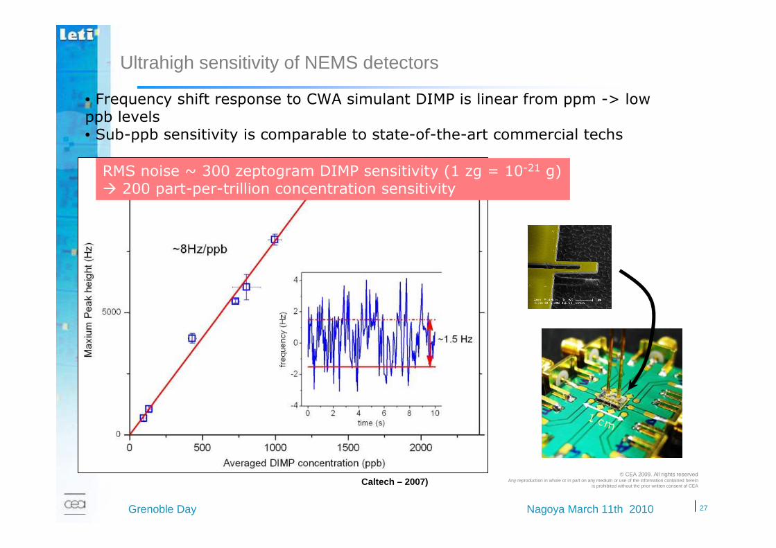
Ultrahigh sensitivity of NEMS detectors
• Frequency shift response to CWA simulant DIMP is linear from ppm -> low ppb levels• Sub-ppb sensitivity is comparable to state-of-the-art commercial techs
RMS noise ~ 300 zeptogram DIMP sensitivity (1 zg = 10-21 g) 200 part-per-trillion concentration sensitivity
Caltech – 2007)

28Grenoble Day Nagoya March 11th 2010
© CEA 2009. All rights reservedAny reproduction in whole or in part on any medium or use of the information contained herein
is prohibited without the prior written consent of CEA
Single NEMS detection
0 2 4 6 8 10 12 14 16 18
−80
−60
−40
−20
0
3.0 ppm
7.5 ppm
15 ppm
30 ppm
75 ppm
150 ppm
1.5 ppm
750 ppb
300 ppb
150 ppb
Fre
quen
cy s
hift
(ppm
)
Time (s)
1 µm
τ = 100 ms
LOD = 150 ppb

29Grenoble Day Nagoya March 11th 2010
© CEA 2009. All rights reservedAny reproduction in whole or in part on any medium or use of the information contained herein
is prohibited without the prior written consent of CEA
Detection with a NEMS array
1 µm
Integration density ~ 60 000 NEMS/mm²Frequency spread < 1% in the array
2,800 NEMS/ array
Array size < 0.05 mm²
Using an array of NEMS allows to:•Reduce the detection time to 1 ms (100x faster)•Increase the detection level to 5 ppb (30x better): SNR ~√N

30Grenoble Day Nagoya March 11th 2010
© CEA 2009. All rights reservedAny reproduction in whole or in part on any medium or use of the information contained herein
is prohibited without the prior written consent of CEA
Analytical module
Detection Data treatment
Everything integrated in a single module, using micro & nano technologies
PC ( x 1000) with Si and CNTs
µGC (for increasing separation power)
NEMS arrays and integrated electronics (ASIC)
Software
On a chip
MGA ArchitecturePre-analytical module
SamplingConcentration
Filtering
µGC
- Selectivity- Sensitivity- Quantitative measurments
Separation

31Grenoble Day Nagoya March 11th 2010
© CEA 2009. All rights reservedAny reproduction in whole or in part on any medium or use of the information contained herein
is prohibited without the prior written consent of CEA
Conclusion
LETI has a strong position in the field of MEMS Experience
Workforce
Number of developments and technology bricks available Number of industrial transfers
New concepts and technologies are being developed to address future needs NEMS for physical sensing (P, acceleration, magnetometer)
NEMS for chemical sensing
NEMS present important potential in terms of
Applications Possibility to combine multiple sensors on a single chip
Level of detection

32Grenoble Day Nagoya March 11th 2010
© CEA 2009. All rights reservedAny reproduction in whole or in part on any medium or use of the information contained herein
is prohibited without the prior written consent of CEA
Thank you for your attention

33Grenoble Day Nagoya March 11th 2010
© CEA 2009. All rights reservedAny reproduction in whole or in part on any medium or use of the information contained herein
is prohibited without the prior written consent of CEA
Innovation
for industry