MEMS .
91
• MEMS https://store.theartofservice.com/itil-2011-foundation-complete-certification-kit-fourth-edition-study-guide-ebook-and- online-course.html
-
Upload
magdalene-logan -
Category
Documents
-
view
213 -
download
1
Transcript of MEMS .

• MEMS
https://store.theartofservice.com/itil-2011-foundation-complete-certification-kit-fourth-edition-study-guide-ebook-and-online-course.html
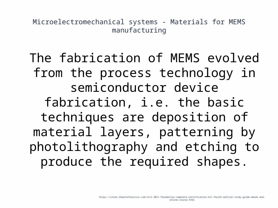
Microelectromechanical systems - Materials for MEMS manufacturing
1 The fabrication of MEMS evolved from the process technology in
semiconductor device fabrication, i.e. the basic techniques are deposition
of material layers, patterning by photolithography and etching to
produce the required shapes.
https://store.theartofservice.com/itil-2011-foundation-complete-certification-kit-fourth-edition-study-guide-ebook-and-online-course.html

Mechanical engineering - Micro electro-mechanical systems (MEMS)
1 Micron-scale mechanical components such as springs, gears, fluidic and heat transfer
devices are fabricated from a variety of substrate materials such as silicon, glass
and polymers like SU8. Examples of MEMS components are the accelerometers that are used as car airbag sensors, modern
cell phones, gyroscopes for precise positioning and microfluidic devices used
in biomedical applications.
https://store.theartofservice.com/itil-2011-foundation-complete-certification-kit-fourth-edition-study-guide-ebook-and-online-course.html
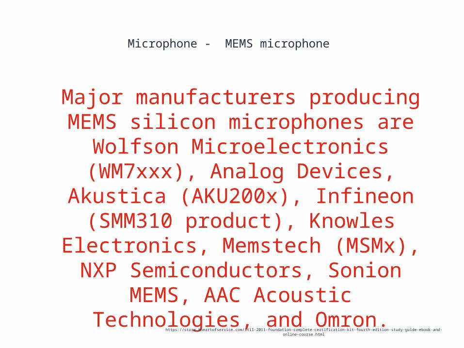
Microphone - MEMS microphone
1 Major manufacturers producing MEMS silicon microphones are
Wolfson Microelectronics (WM7xxx), Analog Devices, Akustica (AKU200x), Infineon (SMM310 product), Knowles Electronics, Memstech (MSMx), NXP Semiconductors, Sonion MEMS, AAC Acoustic Technologies, and Omron.
https://store.theartofservice.com/itil-2011-foundation-complete-certification-kit-fourth-edition-study-guide-ebook-and-online-course.html

Frequency multiplier - Microelectromechanical (MEMS) frequency doubler
1 The inherent square-law nonlinearity of the voltage-to-force transfer function of a cantilever resonator’s capacitive transducer can be employed for the
realization of frequency doubling effect.[http://arxiv.org/abs/1210.3491
Microelectromechanical system cantilever-based frequency doublers] Due to the low-loss attribute (or
equivalently, a high Q) offered by MEMS devices, improved circuit performance can be expected from a
micromechanical frequency doubler than semiconductor devices utilized for the same
task.[http://ieeexplore.ieee.org/stamp/stamp.jsp?tp=arnumber=1386679isnumber=30188 1.156-GHz
self-aligned vibrating micromechanical disk resonator]
https://store.theartofservice.com/itil-2011-foundation-complete-certification-kit-fourth-edition-study-guide-ebook-and-online-course.html
MEMS
1 'Microelectromechanical systems' ('MEMS') (also written as micro-electro-mechanical, MicroElectroMechanical or
microelectronic and microelectromechanical systems) is the technology of very small devices; it merges at the nano-scale into
nanoelectromechanical systems (NEMS) and nanotechnology. MEMS are also referred to
as Micromachinery|micromachines (in Japan), or micro systems technology – MST
(in Europe).https://store.theartofservice.com/itil-2011-foundation-complete-certification-kit-fourth-edition-study-guide-ebook-and-online-course.html

MEMS
1 Because of the large surface area to volume ratio of MEMS, surface
effects such as electrostatics and wetting dominate over volume
effects such as inertia or thermal mass.
https://store.theartofservice.com/itil-2011-foundation-complete-certification-kit-fourth-edition-study-guide-ebook-and-online-course.html

MEMS
1 An early example of a MEMS device is the resonistor – an
electromechanical monolithic resonator.Electromechanical
monolithic resonator, [http://www.google.com/patents/abou
t?id=hpcBAAAAEBAJdq=ELECTROMECHANICAL+MONOLITHIC+RESONATOR US patent 3614677], Filed April 29,
1966; Issued October 1971https://store.theartofservice.com/itil-2011-foundation-complete-certification-kit-fourth-edition-study-guide-ebook-and-online-course.html

MEMS - Silicon
1 Silicon is the material used to create most integrated circuits used in
consumer electronics in the modern industry. The economies of scale, ready availability of cheap high-quality materials and ability to
incorporate electronic functionality make silicon attractive for a wide
variety of MEMS applications.
https://store.theartofservice.com/itil-2011-foundation-complete-certification-kit-fourth-edition-study-guide-ebook-and-online-course.html

MEMS - Silicon
1 Silicon also has significant advantages engendered through its material properties
https://store.theartofservice.com/itil-2011-foundation-complete-certification-kit-fourth-edition-study-guide-ebook-and-online-course.html
MEMS - Polymers
1 MEMS devices can be made from polymers by processes such as injection molding, Embossing (manufacturing)|embossing or
stereolithography and are especially well suited to microfluidic
applications such as disposable blood testing cartridges.
https://store.theartofservice.com/itil-2011-foundation-complete-certification-kit-fourth-edition-study-guide-ebook-and-online-course.html

MEMS - Metals
1 Metals can also be used to create MEMS elements. While metals do not have some of the advantages displayed by silicon in
terms of mechanical properties, when used within their limitations, metals can exhibit very high degrees of reliability. Metals can
be deposited by electroplating, evaporation, and sputtering processes. Commonly used
metals include gold, nickel, aluminium, copper, chromium, titanium, tungsten,
platinum, and silver.https://store.theartofservice.com/itil-2011-foundation-complete-certification-kit-fourth-edition-study-guide-ebook-and-online-course.html

MEMS - Ceramics
1 titanium nitride|TiN, on the other hand, exhibits a high electrical conductivity and large elastic modulus allowing to realize
electrostatic MEMS actuation schemes with ultrathin membranes
https://store.theartofservice.com/itil-2011-foundation-complete-certification-kit-fourth-edition-study-guide-ebook-and-online-course.html
MEMS - Deposition processes
1 One of the basic building blocks in MEMS processing is the ability to
deposit thin films of material with a thickness anywhere between a few
nanometres to about 100 micrometres. There are two types of
deposition processes, as follows.
https://store.theartofservice.com/itil-2011-foundation-complete-certification-kit-fourth-edition-study-guide-ebook-and-online-course.html
MEMS - Physical deposition
1 Physical vapor deposition (PVD) consists of a process in which a
material is removed from a target, and deposited on a surface
https://store.theartofservice.com/itil-2011-foundation-complete-certification-kit-fourth-edition-study-guide-ebook-and-online-course.html

MEMS - Chemical deposition
1 Chemical deposition techniques include chemical vapor deposition (CVD), in
which a stream of source gas reacts on the substrate to grow the material
desired. This can be further divided into categories depending on the details of
the technique, for example, LPCVD (Low Pressure chemical vapor deposition) and
PECVD (Plasma Enhanced chemical vapor deposition).
https://store.theartofservice.com/itil-2011-foundation-complete-certification-kit-fourth-edition-study-guide-ebook-and-online-course.html

MEMS - Chemical deposition
1 Oxide films can also be grown by the technique of thermal oxidation, in
which the (typically silicon) wafer is exposed to oxygen and/or steam, to grow a thin surface layer of silicon
dioxide.
https://store.theartofservice.com/itil-2011-foundation-complete-certification-kit-fourth-edition-study-guide-ebook-and-online-course.html

MEMS - Lithography
1 Lithography in MEMS context is typically the transfer of a pattern into
a photosensitive material by selective exposure to a radiation
source such as light
https://store.theartofservice.com/itil-2011-foundation-complete-certification-kit-fourth-edition-study-guide-ebook-and-online-course.html
MEMS - Lithography
1 This exposed region can then be removed or treated providing a mask
for the underlying substrate. Photolithography is typically used
with metal or other thin film deposition, wet and dry etching.
https://store.theartofservice.com/itil-2011-foundation-complete-certification-kit-fourth-edition-study-guide-ebook-and-online-course.html

MEMS - Photolithography
1 Photolithography is the process of transferring geometric shapes on a
mask to the surface of a silicon wafer. The steps involved in the
photolithographic process are wafer cleaning; barrier layer formation;
photoresist application; soft baking; mask alignment; exposure and development; and hard-baking.
https://store.theartofservice.com/itil-2011-foundation-complete-certification-kit-fourth-edition-study-guide-ebook-and-online-course.html

MEMS - Photolithography
1 In the first step, the wafers are chemically cleaned to remove
particulate matter on the surface as well as any traces of organic, ionic,
and metallic impurities
https://store.theartofservice.com/itil-2011-foundation-complete-certification-kit-fourth-edition-study-guide-ebook-and-online-course.html
MEMS - Photolithography
1 There are two types of photoresist: positive and
negative
https://store.theartofservice.com/itil-2011-foundation-complete-certification-kit-fourth-edition-study-guide-ebook-and-online-course.html
MEMS - Photolithography
1 Negative resists behave in just the opposite manner
https://store.theartofservice.com/itil-2011-foundation-complete-certification-kit-fourth-edition-study-guide-ebook-and-online-course.html

MEMS - Electron beam lithography
1 Electron beam lithography (often abbreviated as e-beam lithography) is the practice of scanning a beam of
electrons in a patterned fashion across a surface covered with a film
(called the resist), (exposing the resist) and of selectively removing
either exposed or non-exposed regions of the resist (developing)
https://store.theartofservice.com/itil-2011-foundation-complete-certification-kit-fourth-edition-study-guide-ebook-and-online-course.html

MEMS - Electron beam lithography
1 The primary advantage of electron beam lithography is that it is one of the ways to beat the diffraction limit
of light and make features in the nanometer regime. This form of
maskless lithography has found wide usage in photomask-making used in
photolithography, low-volume production of semiconductor components, and research
development.https://store.theartofservice.com/itil-2011-foundation-complete-certification-kit-fourth-edition-study-guide-ebook-and-online-course.html

MEMS - Electron beam lithography
1 The key limitation of electron beam lithography is throughput, i.e., the very long time it takes to expose an entire silicon wafer or glass substrate. A long
exposure time leaves the user vulnerable to beam drift or instability which may
occur during the exposure. Also, the turn-around time for reworking or re-design is lengthened unnecessarily if the pattern is
not being changed the second time.
https://store.theartofservice.com/itil-2011-foundation-complete-certification-kit-fourth-edition-study-guide-ebook-and-online-course.html

MEMS - Ion beam lithography
1 It is known that focused-ion-beam lithography has the capability of writing
https://store.theartofservice.com/itil-2011-foundation-complete-certification-kit-fourth-edition-study-guide-ebook-and-online-course.html

MEMS - Ion beam lithography
1 extremely fine lines (less than 50nm line and space has been achieved) without
proximity
https://store.theartofservice.com/itil-2011-foundation-complete-certification-kit-fourth-edition-study-guide-ebook-and-online-course.html

MEMS - Ion beam lithography
1 effect. However, because the writing field in ion-beam
lithography is quite small, large area patterns must be created by stitching together the small fields.
https://store.theartofservice.com/itil-2011-foundation-complete-certification-kit-fourth-edition-study-guide-ebook-and-online-course.html

MEMS - Ion track technology
1 Ion track technology is a deep cutting tool with a resolution limit
around 8nm applicable to radiation resistant minerals, glasses and
polymers
https://store.theartofservice.com/itil-2011-foundation-complete-certification-kit-fourth-edition-study-guide-ebook-and-online-course.html

MEMS - X-ray lithography
1 X-ray lithography, is a process used in electronic industry to selectively
remove parts of a thin film. It uses X-rays to transfer a geometric pattern
from a mask to a light-sensitive chemical photoresist, or simply
resist, on the substrate. A series of chemical treatments then engraves
the produced pattern into the material underneath the photoresist.
https://store.theartofservice.com/itil-2011-foundation-complete-certification-kit-fourth-edition-study-guide-ebook-and-online-course.html
MEMS - Etching processes
1 In the former, the material is dissolved when immersed in a chemical solution.
https://store.theartofservice.com/itil-2011-foundation-complete-certification-kit-fourth-edition-study-guide-ebook-and-online-course.html

MEMS - Etching processes
1 In the latter, the material is sputtered or dissolved using reactive ions or a vapor phase etchant. for a somewhat dated overview of MEMS
etching technologies.
https://store.theartofservice.com/itil-2011-foundation-complete-certification-kit-fourth-edition-study-guide-ebook-and-online-course.html

MEMS - Wet etching
1 Wet chemical etching consists in selective removal of material by
dipping a substrate into a solution that dissolves it. The chemical nature
of this etching process provides a good selectivity, which means the
etching rate of the target material is considerably higher than the mask
material if selected carefully.
https://store.theartofservice.com/itil-2011-foundation-complete-certification-kit-fourth-edition-study-guide-ebook-and-online-course.html

MEMS - Isotropic etching
1 Etching progresses at the same speed in all directions. Long and
narrow holes in a mask will produce v-shaped grooves in the silicon. The
surface of these grooves can be atomically smooth if the etch is
carried out correctly, with dimensions and angles being extremely
accurate.
https://store.theartofservice.com/itil-2011-foundation-complete-certification-kit-fourth-edition-study-guide-ebook-and-online-course.html

MEMS - Anisotropic etching
1 Some single crystal materials, such as silicon, will have different etching
rates depending on the crystallographic orientation of the
substrate
https://store.theartofservice.com/itil-2011-foundation-complete-certification-kit-fourth-edition-study-guide-ebook-and-online-course.html

MEMS - HF etching
1 Hydrofluoric acid is commonly used as an aqueous etchant for silicon
dioxide (, also known as BOX for SOI), usually in 49% concentrated form,
5:1, 10:1 or 20:1 BOE (buffered oxide etchant) or BHF (Buffered HF). They were first used in medieval times for
glass etching. It was used in IC fabrication for patterning the gate oxide until the process step was
replaced by RIE.https://store.theartofservice.com/itil-2011-foundation-complete-certification-kit-fourth-edition-study-guide-ebook-and-online-course.html
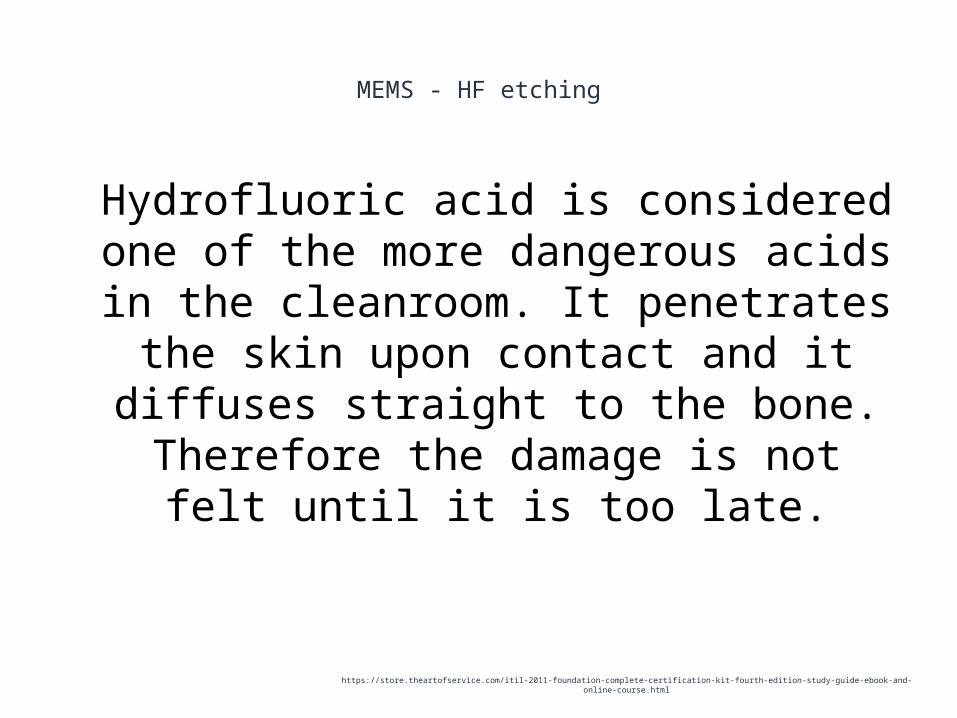
MEMS - HF etching
1 Hydrofluoric acid is considered one of the more dangerous acids in the cleanroom. It penetrates the skin
upon contact and it diffuses straight to the bone. Therefore the damage is
not felt until it is too late.
https://store.theartofservice.com/itil-2011-foundation-complete-certification-kit-fourth-edition-study-guide-ebook-and-online-course.html

MEMS - Electrochemical etching
1 Electrochemical etching (ECE) for dopant-selective removal of silicon is a common method to automate and
to selectively control etching
https://store.theartofservice.com/itil-2011-foundation-complete-certification-kit-fourth-edition-study-guide-ebook-and-online-course.html
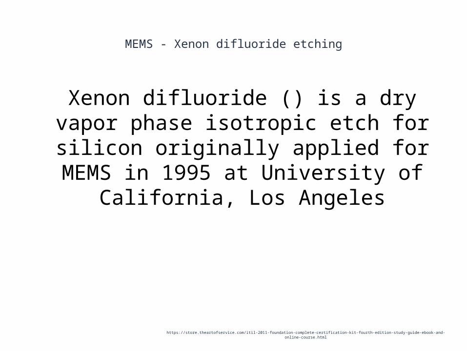
MEMS - Xenon difluoride etching
1 Xenon difluoride () is a dry vapor phase isotropic etch for silicon
originally applied for MEMS in 1995 at University of California, Los
Angeles
https://store.theartofservice.com/itil-2011-foundation-complete-certification-kit-fourth-edition-study-guide-ebook-and-online-course.html
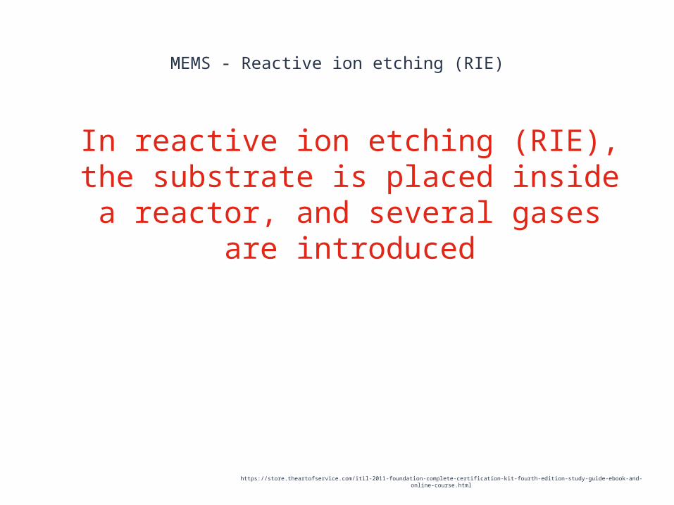
MEMS - Reactive ion etching (RIE)
1 In reactive ion etching (RIE), the substrate is placed inside a reactor, and several gases are introduced
https://store.theartofservice.com/itil-2011-foundation-complete-certification-kit-fourth-edition-study-guide-ebook-and-online-course.html

MEMS - Reactive ion etching (RIE)
1 Deep RIE (DRIE) is a special subclass of RIE
that is growing in popularity
https://store.theartofservice.com/itil-2011-foundation-complete-certification-kit-fourth-edition-study-guide-ebook-and-online-course.html

MEMS - Reactive ion etching (RIE)
1 The creates a polymer on the surface of the substrate, and the second gas composition ( and )
etches the substrate
https://store.theartofservice.com/itil-2011-foundation-complete-certification-kit-fourth-edition-study-guide-ebook-and-online-course.html
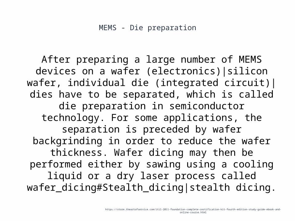
MEMS - Die preparation
1 After preparing a large number of MEMS devices on a wafer (electronics)|silicon wafer, individual die (integrated circuit)|dies have to be separated, which is called die preparation
in semiconductor technology. For some applications, the separation is preceded by wafer backgrinding in order to reduce the wafer thickness. Wafer dicing may then be performed either by sawing using a cooling
liquid or a dry laser process called wafer_dicing#Stealth_dicing|stealth dicing.
https://store.theartofservice.com/itil-2011-foundation-complete-certification-kit-fourth-edition-study-guide-ebook-and-online-course.html

MEMS - Bulk micromachining
1 Bulk micromachining is the oldest paradigm of silicon
based MEMS
https://store.theartofservice.com/itil-2011-foundation-complete-certification-kit-fourth-edition-study-guide-ebook-and-online-course.html

MEMS - Surface micromachining
1 Analog Devices have pioneered the industrialization of surface
micromachining and have realized the co-integration of MEMS and
integrated circuits.
https://store.theartofservice.com/itil-2011-foundation-complete-certification-kit-fourth-edition-study-guide-ebook-and-online-course.html

MEMS - High aspect ratio (HAR) silicon micromachining
1 Bonding a second wafer by glass frit bonding, anodic bonding or alloy
bonding is used to protect the MEMS structures
https://store.theartofservice.com/itil-2011-foundation-complete-certification-kit-fourth-edition-study-guide-ebook-and-online-course.html
MEMS - Applications
1 In one viewpoint MEMS application is categorized by
type of use.
https://store.theartofservice.com/itil-2011-foundation-complete-certification-kit-fourth-edition-study-guide-ebook-and-online-course.html
MEMS - Applications
1 In another view point MEMS applications are categorized by the
field of application (commercial applications include):
https://store.theartofservice.com/itil-2011-foundation-complete-certification-kit-fourth-edition-study-guide-ebook-and-online-course.html

MEMS - Applications
1 *Inkjet printers, which use piezoelectrics or thermal bubble ejection to deposit ink on
paper.
https://store.theartofservice.com/itil-2011-foundation-complete-certification-kit-fourth-edition-study-guide-ebook-and-online-course.html

MEMS - Applications
1 *Accelerometers in modern cars for a large number of purposes including
airbag deployment in collisions.
https://store.theartofservice.com/itil-2011-foundation-complete-certification-kit-fourth-edition-study-guide-ebook-and-online-course.html

MEMS - Applications
1 [ http://www.eetimes.com/showArticle.j
html?articleID=200900669 There's more to MEMS than meets the
iPhone], EE Times, (2007-07-09) and a number of Digital Cameras (various
Canon Digital IXUS models)
https://store.theartofservice.com/itil-2011-foundation-complete-certification-kit-fourth-edition-study-guide-ebook-and-online-course.html

MEMS - Applications
1 *MEMS gyroscopes used in modern cars and other applications to detect
yaw, pitch, and roll|yaw; e.g., to deploy a roll over bar or trigger
dynamic stability control
https://store.theartofservice.com/itil-2011-foundation-complete-certification-kit-fourth-edition-study-guide-ebook-and-online-course.html
MEMS - Applications
1 *Silicon pressure sensors e.g., car tire pressure sensors, and disposable blood
pressure sensors
https://store.theartofservice.com/itil-2011-foundation-complete-certification-kit-fourth-edition-study-guide-ebook-and-online-course.html

MEMS - Applications
1 *Display device|Displays e.g., the Digital micromirror device|DMD chip in a projector based on Digital Light Processing|DLP technology, which has a surface with several hundred
thousand micromirrors or single micro-scanning-mirrors also called
microscanners
https://store.theartofservice.com/itil-2011-foundation-complete-certification-kit-fourth-edition-study-guide-ebook-and-online-course.html

MEMS - Applications
1 *Optical switching technology, which is used for switching technology and alignment for data communications
https://store.theartofservice.com/itil-2011-foundation-complete-certification-kit-fourth-edition-study-guide-ebook-and-online-course.html
MEMS - Applications
1 *Bio-MEMS applications in medical and health related technologies from Lab-On-Chip to
MicroTotalAnalysis (biosensor, chemosensor), or embedded in medical devices e.g. stents.
[ http://ves.sagepub.com/content/46/8/605 Microelectromechanical Systems and
Nanotechnology. A Platform for the Next Stent Technological Era ,Louizos-Alexandros Louizos,
Panagiotis G. Athanasopoulos, Kevin Varty,VASC ENDOVASCULAR SURG November 2012 vol. 46
no. 8 605-609, doi: 10.1177/1538574412462637]
https://store.theartofservice.com/itil-2011-foundation-complete-certification-kit-fourth-edition-study-guide-ebook-and-online-course.html

MEMS - Applications
1 *Interferometric modulator display (IMOD) applications in consumer electronics (primarily displays for mobile devices), used to create interferometric modulation −
reflective display technology as found in mirasol displays
https://store.theartofservice.com/itil-2011-foundation-complete-certification-kit-fourth-edition-study-guide-ebook-and-online-course.html

MEMS - Applications
1 *electrostatic fluid accelerator|Fluid acceleration such as for micro-cooling
https://store.theartofservice.com/itil-2011-foundation-complete-certification-kit-fourth-edition-study-guide-ebook-and-online-course.html

MEMS - Applications
1 *Micro-scale Energy harvesting including piezoelectric, electrostatic
and electromagentic micro harvesters.
https://store.theartofservice.com/itil-2011-foundation-complete-certification-kit-fourth-edition-study-guide-ebook-and-online-course.html

MEMS - Applications
1 *Micromachined Ultrasound Transducer including Piezoelectric
Micromachined Ultrasonic Transducers and Capacitive Micromachined Ultrasonic
Transducers.
https://store.theartofservice.com/itil-2011-foundation-complete-certification-kit-fourth-edition-study-guide-ebook-and-online-course.html
MEMS - Applications
1 Companies with strong MEMS programs come in many sizes. The larger firms specialize in
manufacturing high volume inexpensive components or packaged solutions for end markets such as automobiles, biomedical,
and electronics. The successful small firms provide value in innovative solutions and absorb the expense of custom fabrication with high sales margins. In addition, both large and small companies work in RD to
explore MEMS technology.
https://store.theartofservice.com/itil-2011-foundation-complete-certification-kit-fourth-edition-study-guide-ebook-and-online-course.html
MEMS - Industry structure
1 The global market for micro-electromechanical systems, which includes products such as
automobile airbag systems, display systems and inkjet cartridges totaled $40 billion in 2006
according to Global MEMS/Microsystems Markets and Opportunities, a research report from SEMI and Yole Developpement and is forecasted to
reach $72 billion by 2011.[http://www.azonano.com/news.asp?
newsID=4479 Worldwide MEMS Systems Market Forecasted to Reach $72 Billion by 2011]
https://store.theartofservice.com/itil-2011-foundation-complete-certification-kit-fourth-edition-study-guide-ebook-and-online-course.html

MEMS - Industry structure
1 While MEMS manufacturing continues to be dominated by used
semiconductor equipment, there is a migration to 200mm lines and select
new tools, including etch and bonding for certain MEMS
applications.
https://store.theartofservice.com/itil-2011-foundation-complete-certification-kit-fourth-edition-study-guide-ebook-and-online-course.html

Wavelength selective switching - Microelectromechanical Mirrors (MEMS)
1 The incoming light is broken into a spectrum by a diffraction grating
(shown at RHS of Figure) and each wavelength channel then focuses on
a separate MEMS mirror
https://store.theartofservice.com/itil-2011-foundation-complete-certification-kit-fourth-edition-study-guide-ebook-and-online-course.html
Wavelength selective switching - Microelectromechanical Mirrors (MEMS)
1 This technology has the advantage of a single steering surface, not
necessarily requiring polarization diversity optics. It works well in the
presence of a continuous signal, allowing the mirror tracking circuits to dither the mirror and maximise
coupling.
https://store.theartofservice.com/itil-2011-foundation-complete-certification-kit-fourth-edition-study-guide-ebook-and-online-course.html
Wavelength selective switching - Microelectromechanical Mirrors (MEMS)
1 MEMS based WSS typically produce good extinction ratios, but poor open loop performance for setting a given
attenuation level
https://store.theartofservice.com/itil-2011-foundation-complete-certification-kit-fourth-edition-study-guide-ebook-and-online-course.html

Wavelength selective switching - MEMS Arrays
1 In this case, the angle of the MEMs mirrors is changed to
deflect the beam
https://store.theartofservice.com/itil-2011-foundation-complete-certification-kit-fourth-edition-study-guide-ebook-and-online-course.html

MEMS magnetometer - Introduction
1 Magnetic field sensors|Magnetic field sensing can be categorized into four general typesLenz, J., Edelstein, A.S.,
Magnetic sensors and their applications
https://store.theartofservice.com/itil-2011-foundation-complete-certification-kit-fourth-edition-study-guide-ebook-and-online-course.html

MEMS magnetometer - Introduction
1 Integration of MEMS sensor and microelectronics can further reduce the size of the entire magnetic field
sensing system.
https://store.theartofservice.com/itil-2011-foundation-complete-certification-kit-fourth-edition-study-guide-ebook-and-online-course.html
MEMS magnetometer - Lorentz-force-based MEMS sensor
1 This type sensor relies on the mechanical motion of the MEMS
structure due to the Lorentz force acting on the current-carrying
conductor in the magnetic field
https://store.theartofservice.com/itil-2011-foundation-complete-certification-kit-fourth-edition-study-guide-ebook-and-online-course.html

MEMS magnetometer - Voltage sensing
1 Beroulle et al.Beroulle, V.; Bertrand, Y.; Latorre, L.; Nouet,
P
https://store.theartofservice.com/itil-2011-foundation-complete-certification-kit-fourth-edition-study-guide-ebook-and-online-course.html
MEMS magnetometer - Voltage sensing
1 Herrera-May et al.Herrera-May, A.L.; García-Ramírez, P.J.; Aguilera-Cortés, L.A.; Martínez-Castillo, J.; Sauceda-Carvajal, A.; García-González, L.;
Figueras-Costa, E
https://store.theartofservice.com/itil-2011-foundation-complete-certification-kit-fourth-edition-study-guide-ebook-and-online-course.html

MEMS magnetometer - Voltage sensing
1 Kádár et al.Kádár, Z.; Bossche, A.; Sarro, P.M.;
Mollinger, J.R
https://store.theartofservice.com/itil-2011-foundation-complete-certification-kit-fourth-edition-study-guide-ebook-and-online-course.html
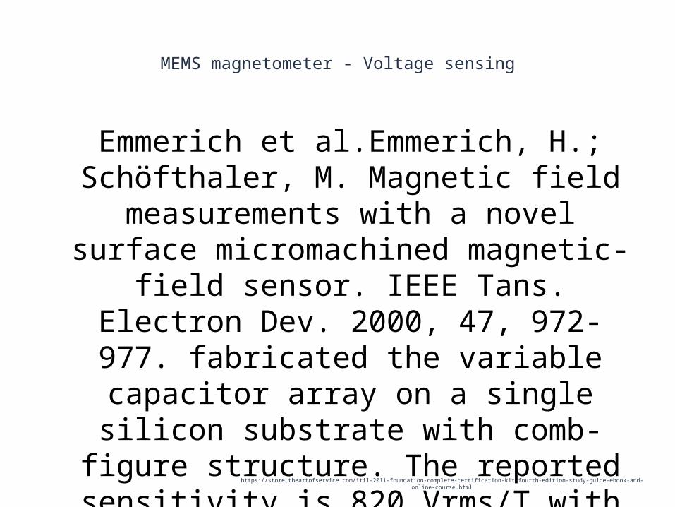
MEMS magnetometer - Voltage sensing
1 Emmerich et al.Emmerich, H.; Schöfthaler, M. Magnetic field
measurements with a novel surface micromachined magnetic-field sensor. IEEE Tans. Electron Dev.
2000, 47, 972-977. fabricated the variable capacitor array on a single silicon substrate with comb-figure
structure. The reported sensitivity is 820 Vrms/T with a resolution 200 nT
at the pressure level of 1mbar.https://store.theartofservice.com/itil-2011-foundation-complete-certification-kit-fourth-edition-study-guide-ebook-and-online-course.html
MEMS magnetometer - Frequency shift sensing
1 Another type of Lorentz force based MEMS magnetic field sensor utilize the shift of mechanical resonance
due to the Lorentz force applying to certain mechanical structures.
https://store.theartofservice.com/itil-2011-foundation-complete-certification-kit-fourth-edition-study-guide-ebook-and-online-course.html

MEMS magnetometer - Frequency shift sensing
1 Sunier et al.Sunier, R.; Vancura, T.; Li, Y.; Kay-Uwe, K.; Baltes, H.; Brand, O
https://store.theartofservice.com/itil-2011-foundation-complete-certification-kit-fourth-edition-study-guide-ebook-and-online-course.html

MEMS magnetometer - Frequency shift sensing
1 Bahreyni et al.Bahreyni, B.;
Shafai, C
https://store.theartofservice.com/itil-2011-foundation-complete-certification-kit-fourth-edition-study-guide-ebook-and-online-course.html

MEMS magnetometer - Optical sensing
1 The optical sensing is to directly measure the mechanical
displacement of the MEMS structure to find the external magnetic field.
https://store.theartofservice.com/itil-2011-foundation-complete-certification-kit-fourth-edition-study-guide-ebook-and-online-course.html
MEMS magnetometer - Optical sensing
1 Zanetti et al.Zanetti, L.J.; Potemra, T.A.; Oursler, D.A.; Lohr, D.A.; Anderson, B.J.; Givens, R.B.;
Wickenden, D.K.; Osiander, R.; Kistenmacher, T.J.; Jenkins, R.E
https://store.theartofservice.com/itil-2011-foundation-complete-certification-kit-fourth-edition-study-guide-ebook-and-online-course.html

MEMS magnetometer - Optical sensing
1 Keplinger et al.Keplinger, F.; Kvasnica, S.; Hauser, H.;
Grössinger, R
https://store.theartofservice.com/itil-2011-foundation-complete-certification-kit-fourth-edition-study-guide-ebook-and-online-course.html

MEMS magnetometer -
1 When the temperature increases, the Young’s modulus of the material used
to fabricate the moving structure decreases
https://store.theartofservice.com/itil-2011-foundation-complete-certification-kit-fourth-edition-study-guide-ebook-and-online-course.html

IBM Monochrome Display Adapter - Clone boardshttp://www.vgamuseum.info/index.php/component/content/arti
cle/59-vlasks-articles/index.php?optioncom_custompropertiesviewshowtaskshowcp_madecp_buscp_memsizecp_yearcp_memorycp_familycp_cardtypemdacp_ownercp_directxcp_openglcp_pipelinescp_manufacturercp_processcp_text_search
1 Other boards offered MDA compatibility, although with
differences on how attributes are displayed or the font used.
https://store.theartofservice.com/itil-2011-foundation-complete-certification-kit-fourth-edition-study-guide-ebook-and-online-course.html

IBM Monochrome Display Adapter - Clone boardshttp://www.vgamuseum.info/index.php/component/content/arti
cle/59-vlasks-articles/index.php?optioncom_custompropertiesviewshowtaskshowcp_madecp_buscp_memsizecp_yearcp_memorycp_familycp_cardtypemdacp_ownercp_directxcp_openglcp_pipelinescp_manufacturercp_processcp_text_search
1 *United Microelectronics
Corporation UM6845
https://store.theartofservice.com/itil-2011-foundation-complete-certification-kit-fourth-edition-study-guide-ebook-and-online-course.html

Hercules Graphics Card - Clone boards[http://www.vgamuseum.info/index.php/component/content/art
icle/59-vlasks-articles/index.php?optioncom_custompropertiesviewshowtaskshowcp_madecp_buscp_memsizecp_yearcp_memorycp_familycp_cardtypeherculescp_ownercp_directxcp_openglcp_pipelinescp_manufacturercp_processcp_text_sear
ch VGA Legacy]
1 Other boards offered Hercules
compatibility.
https://store.theartofservice.com/itil-2011-foundation-complete-certification-kit-fourth-edition-study-guide-ebook-and-online-course.html

Hercules Graphics Card - Clone boards[http://www.vgamuseum.info/index.php/component/content/art
icle/59-vlasks-articles/index.php?optioncom_custompropertiesviewshowtaskshowcp_madecp_buscp_memsizecp_yearcp_memorycp_familycp_cardtypeherculescp_ownercp_directxcp_openglcp_pipelinescp_manufacturercp_processcp_text_sear
ch VGA Legacy]
1 *ATi Small Wonder Graphics Solution, 18700, Graphics
Solution Plus
https://store.theartofservice.com/itil-2011-foundation-complete-certification-kit-fourth-edition-study-guide-ebook-and-online-course.html

Barometric - Mems Barometers
1 Microelectromechanical systems (or Mems) barometers are extremely small devices between 1 to 100 micrometres in size (i.e. 0.001 to
0.1mm). They are created via lithography or etching. Typical
applications include miniaturized weather stations, electronic barometers and altimeters.
https://store.theartofservice.com/itil-2011-foundation-complete-certification-kit-fourth-edition-study-guide-ebook-and-online-course.html

COMSOL Multiphysics - MEMS Module
1 For coupled physical processes in microelectromechanical systems and piezoelectric devices. Incorporates specific multiphysics couplings for
applications such as thin-film damping, piezoelectricity, and fluid-structure interaction. A specialized user interface for electromechanics interactions is included that allows
for MEMS cantilever beam simulations.
https://store.theartofservice.com/itil-2011-foundation-complete-certification-kit-fourth-edition-study-guide-ebook-and-online-course.html
List of Freescale products - MEMS Sensors
1 * MMA Series (Multi-G/ Multi-Axis
Accelerometers)
https://store.theartofservice.com/itil-2011-foundation-complete-certification-kit-fourth-edition-study-guide-ebook-and-online-course.html

Jaypee Institute of Information Technology - MEMS Design Centre
1 The Centre has undertaken in-house development of Quartz Micro-balance
for Bio-sensors, MEMS Inductor Design for RF wireless application, Microcantilever for communication filter and lead free piezo ceramics
through master level projects.
https://store.theartofservice.com/itil-2011-foundation-complete-certification-kit-fourth-edition-study-guide-ebook-and-online-course.html
For More Information, Visit:
• https://store.theartofservice.com/itil-2011-foundation-complete-certification-kit-fourth-edition-study-guide-ebook-and-online-course.html
The Art of Servicehttps://store.theartofservice.com