Memory design - All Faculty | Duke Electrical and Computer...
38
Memory Design • Memory Types • Memory Organization • ROM design • RAM design • PLA design Adapted from J. M. Rabaey, A. Chandrakasan and B. Nikolic, Digital Integrated Circuits, 2 nd ed. Copyright 2003 Prentice Hall/Pearson. ECE 261 James Morizio 1
Transcript of Memory design - All Faculty | Duke Electrical and Computer...

Memory Design
• Memory Types• Memory Organizationy g• ROM design• RAM designg• PLA design
Adapted from J. M. Rabaey, A. Chandrakasan and B. Nikolic, Digital Integrated Circuits, 2nd ed. Copyright 2003 Prentice Hall/Pearson.
ECE 261 James Morizio 1

Semiconductor MemorySemiconductor Memory Classification
Read-Write MemoryNon-VolatileRead-Write
MemoryRead-Only Memory
EPROM
E2PROM
RandomAccess
Non-RandomAccess Mask-Programmed
P bl (PROM)E PROM
FLASHSRAM
DRAM
Programmable (PROM)
FIFO
LIFODRAMShift Register
CAM
ECE 261 James Morizio 2

M Ti i D fi i iMemory Timing: DefinitionsRead cycle
Write cycle
y
READ
Write cycleRead access Read access
Write access
WRITE
Write accessData valid
DATA
Data written
DATA
ECE 261 James Morizio 3

Memory Architecture: yDecodersM bits M bits
S0 S0Word 0
Word 1
Word 2 Storagecell
S0
S1
S2A 0
A 1
Word 0
Word 1
Word 2 Storagecell
S0
Word N 2 2NwordsSN 2 2A K 2 1
SWord N 2 2Decoder
Word N 2 1K 5 log2N
SN 2 1 Word N 2 1
Input-Output(M bits)
Intuitive architecture for N x M memoryToo many select signals:
N d N l t i lK = log2N
Decoder reduces the number of select signals
Input-Output(M bits)
ECE 261 James Morizio 4
N words == N select signals 2

Array-Structured Memory Architecture
Bit line2L 2 KStorage cell
Problem: ASPECT RATIO or HEIGHT >> WIDTH
Dec
oder
Word line
AK
AK1 1R
owAL 2 1
M.2K
A0
M.2
Sense amplifiers / Drivers Amplify swing torail-to-rail amplitude
0
AK2 1Column decoder
Input-Output
Selects appropriateword
ECE 261 James Morizio 5
p p(M bits)

Hierarchical Memory ArchitectureHierarchical Memory ArchitectureBlock 0
Rowdd
Block i Block P 2 1
address
Columnaddress
Blockaddress
Globalamplifier/driver
Controlcircuitry
Global data busBlock selector
Advantages:Advantages:1. Shorter wires within blocks1. Shorter wires within blocks
I/O
ECE 261 James Morizio 6
1. Shorter wires within blocks1. Shorter wires within blocks2. Block address activates only 1 block => power savings2. Block address activates only 1 block => power savings

R d O l M C llRead-Only Memory CellsBL BLBL
VWL
WL1
WL
VDD
BL BL BL
WL WL
0WL
GND
Diode ROM MOS ROM 1 MOS ROM 2
ECE 261 James Morizio 7
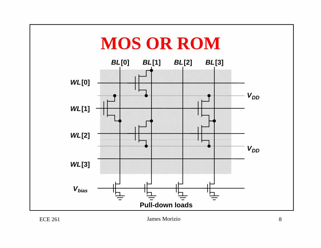
MOS OR ROMMOS OR ROMBL[0] BL[1] BL[2] BL[3]
WL[0]
VDD
WL[1]WL[1]
WL[2]
WL[3]
VDD
Vbias
ECE 261 James Morizio 8
Pull-down loads

ROM ExampleROM Example• 4-word x 6-bit ROM Word 0: 010101
– Represented with dot diagram– Dots indicate 1’s in ROM
Word 1: 011001
Word 2: 100101
101010weak Word 3: 101010A0A1
weakpseudo-nMOS
pullups
ROM Array
2:4DEC
y
Y0Y1Y2Y3Y4Y5
Looks like 6 4 input pseudo nMOS NORs
ECE 261 James Morizio 9
Looks like 6 4-input pseudo-nMOS NORs

MOS NOR ROMMOS NOR ROMVDD
Pull up devices
WL[0]
Pull-up devices
GND
WL [1]
WL [2]
GND
BL [0]
WL [3]
BL [1] BL [2] BL [3]
ECE 261 James Morizio 10
BL [0] BL [1] BL [2] BL [3]

MOS NOR ROM LayoutCell (9.5λ x 7λ)
Programmming using theActive Layer Onlyy y
Polysilicon
Metal1
Diffusion
Metal1 on Diffusion
ECE 261 James Morizio 11

MOS NOR ROM LayoutCell (11λ x 7λ)Cell (11λ x 7λ)
Programmming usingthe Contact Layer Only
Polysilicon
Metal1
Diffusion
Metal1 on Diffusion
ECE 261 James Morizio 12

MOS NAND ROMVDD
Pull-up devices
WL [0]
BL[3]BL[2]BL[1]BL [0]
WL [1]
WL [2]
WL [3]
All word lines high by default with exception of selected row
ECE 261 James Morizio 13
All word lines high by default with exception of selected row

MOS NAND ROM LayoutMOS NAND ROM LayoutCell (8λ x 7λ)P i iProgrammming usingthe Metal-1 Layer Only
No contact to VDD or GND necessary;
Loss in performance compared to NOR ROMdrastically reduced cell size
Polysilicon
Diffusion
Metal1 on Diffusion
ECE 261 James Morizio 14

NAND ROM LayoutCell (5λ x 6λ)
P i iProgrammming usingImplants Only
Polysilicon
Threshold-alteringimplantimplant
Metal1 on Diffusion
ECE 261 James Morizio 15

Decreasing Word Line Delayg yPolysilicon word lineWL
Driver
Metal word line
Metal bypass
(a) Driving the word line from both sides
Polysilicon word lineK cellsWL
(b) Using a metal bypass
ECE 261 James Morizio 16

Precharged MOS NOR ROMgVDD
Precharge devices
pref
WL [0]
GNDWL [1]WL [1]
WL [2]
WL [3]
GND
PMOS precharge device can be made as large as necessary,but clock driver becomes harder to design
BL [0] BL [1] BL [2] BL [3]
ECE 261 James Morizio 17
but clock driver becomes harder to design.
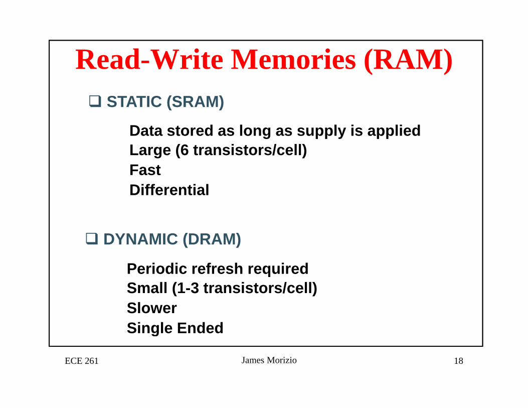
Read-Write Memories (RAM)STATIC (SRAM)
D t t d l l i li dData stored as long as supply is appliedLarge (6 transistors/cell)FastDifferential
DYNAMIC (DRAM)
Periodic refresh requiredSmall (1-3 transistors/cell)SlowerSingle Ended
ECE 261 James Morizio 18
Single Ended

6 transistor CMOS SRAM Cell6-transistor CMOS SRAM Cell WLWL
VDDM4M2
M5M6
42
M1 M3
BLBL
ECE 261 James Morizio 19
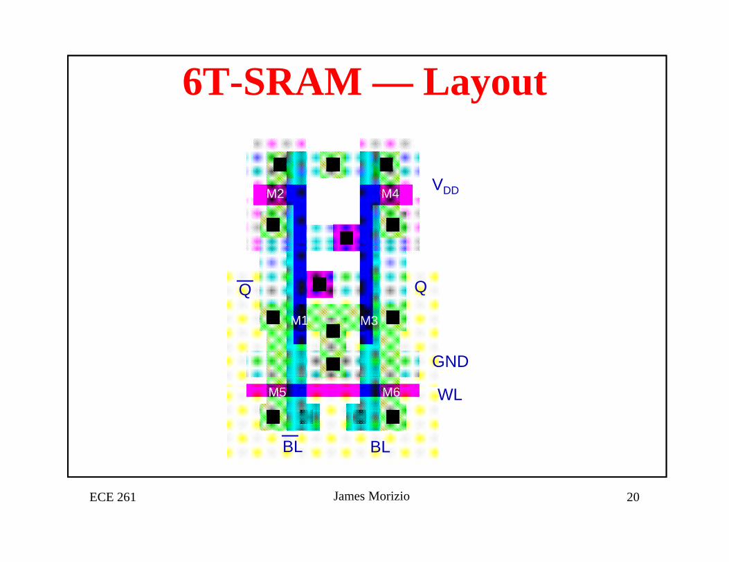
6T-SRAM — Layout
VDDM4M2
M1 M3
GND
M1 M3
M5 M6 WL
BLBL
M5 M6
ECE 261 James Morizio 20

Statue of Goethe and Schiller: the German National Theater, Weimar
ECE 261 James Morizio 21

3-Transistor DRAM Cell
WWL
BL1 BL2
WWL
M3
RWL
RWL
WWL
M1 X
3
M2
CS BL 1
X
BL 2
No constraints on device ratiosReads are non-destructive
ECE 261 James Morizio 22
Value stored at node X when writing a “1” = VWWL-VTn

3T-DRAM — Layout
BL2 BL1 GND
RWLM3M3
M2
WWLM1
ECE 261 James Morizio 23
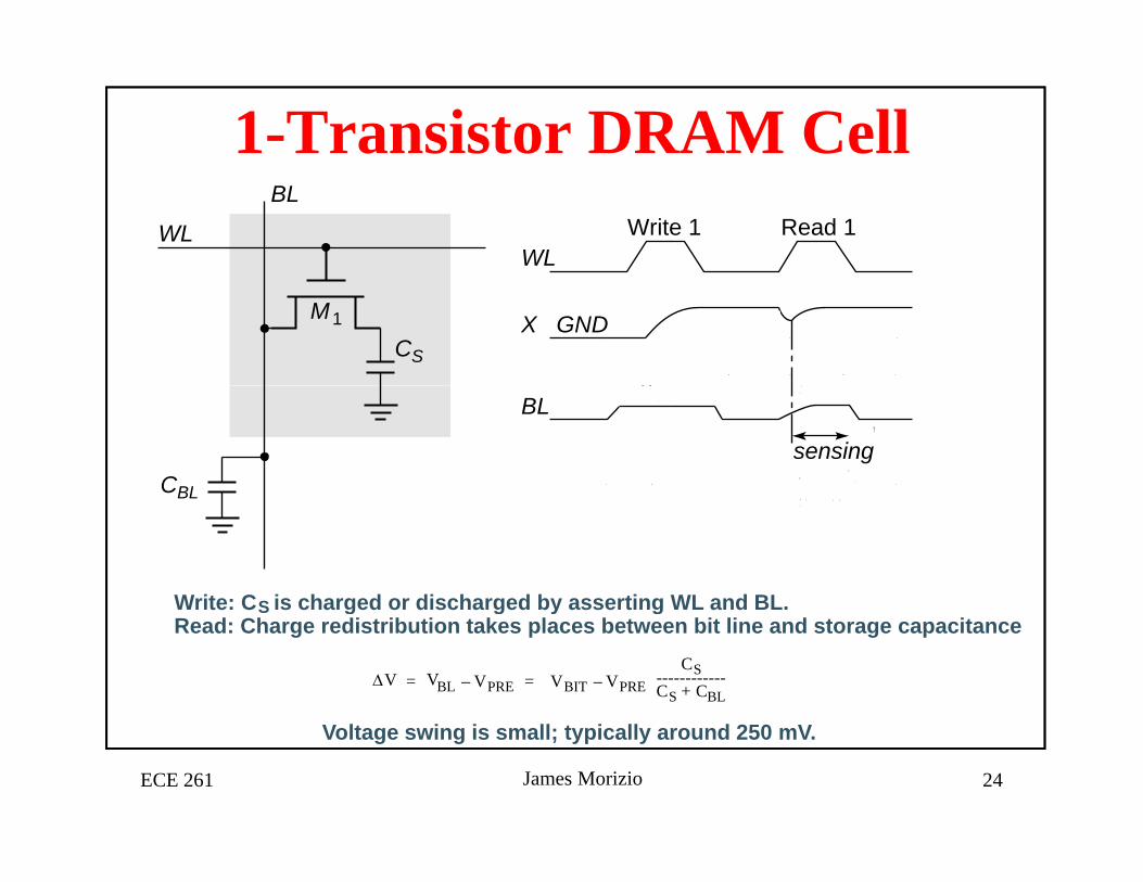
1-Transistor DRAM CellWL
BL
WLWrite 1 Read 1
M1
CS
VDD 2 VTX GND
V
CBL
sensing
BLVDD
VDD /2 VDD /2
Write: CS is charged or discharged by asserting WL and BL.
BL
Write: CS is charged or discharged by asserting WL and BL.Read: Charge redistribution takes places between bit line and storage capacitance
ΔV BL VPRE– VBIT VPRE–CS
CS CBL+------------= =V
ECE 261 James Morizio 24
Voltage swing is small; typically around 250 mV.

DRAM Cell Observations1T DRAM requires a sense amplifier for each bit line, due to
charge redistribution read-out.DRAM ll i l d d i SRAMDRAM memory cells are single-ended in contrast to SRAM
cells.The read-out of the 1T DRAM cell is destructive; read and f h ti f t tirefresh operations are necessary for correct operation.Unlike 3T cell, 1T cell requires presence of an extra
capacitance that must be explicitly included in the design.When writing a “1” into a DRAM cell, a threshold voltage is
lost. This charge loss can be circumvented by bootstrapping the word lines to a higher value than VDD
ECE 261 James Morizio 25

1-T DRAM CellCapacitor
M1 wordline
Metal word lineSiO2
Poly
Diffusedbit linePoly
Field Oxiden+ n+
Inversion layerinduced byplate bias
Polysilicongate
Polysiliconplate
Cross-section Layout
plate bias
Uses Polysilicon-Diffusion CapacitanceExpensive in Area (trend now is to use trench capacitors
Cross section Layout
ECE 261 James Morizio 26
Expensive in Area (trend now is to use trench capacitors

Peripheryp y
DecodersSense AmplifierspInput/Output BuffersControl / Timing CircuitryControl / Timing Circuitry
ECE 261 James Morizio 27
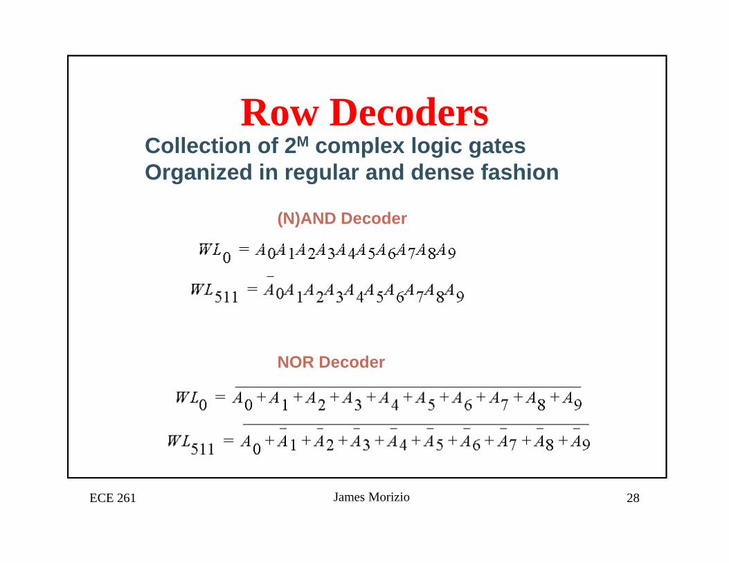
R D dRow DecodersCollection of 2M complex logic gatesOrganized in regular and dense fashionOrganized in regular and dense fashion
(N)AND Decoder
NOR Decoder
ECE 261 James Morizio 28
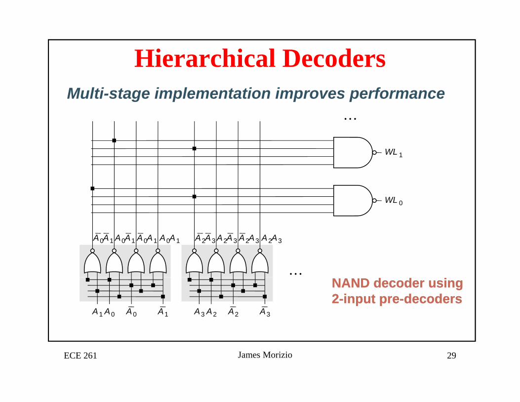
Hierarchical Decoders
• • •
Multi-stage implementation improves performance
WL 1
WL 0
• • •
A2A3A2A3A2A3A2A3A0A1A0A1A0A1A0A1
A2A2A3 A3A0A0A1 A1
NAND decoder usingNAND decoder using22--input preinput pre--decodersdecoders
ECE 261 James Morizio 29

D namic DecodersDynamic DecodersPrecharge devices GND GND VDD
WL3
WL3
WL
VDD
WL2
WL1
WL
WL 2
WL 1
VDD
VDD
VDD φ
WL0
A0A0 A1A1φA0A0 A1A1
WL 0
2-input NOR decoder 2-input NAND decoder
ECE 261 James Morizio 30

4-to-1 tree based column decoderBL 0 BL 1 BL 2 BL 3
A 0
A 0
A1A1
A 1
DNumber of devices drastically reducedDelay increases quadratically with # of sections; prohibitive for large decoders
buffersprogressive sizing
bi ti f t d t i t h
Solutions:
D
ECE 261 James Morizio 31
combination of tree and pass transistor approaches

PLA versus ROMProgrammable Logic Arraystructured approach to random logic“two level logic implementation”
NOR-NOR (product of sums)NAND-NAND (sum of products)
SIMILAR TO ROMSIMILAR TO ROM
Main differenceROM: fully populatedROM: fully populatedPLA: one element per minterm
Note: Importance of PLA’s has drastically reducedp y1. slow2. better software techniques (mutli-level logic
synthesis)B t
ECE 261 James Morizio 32
But …

Programmable Logic ArrayP d NMOS PLA
GND GND GND GND GND
V DD
Pseudo-NMOS PLA
GND
GND
V DD X 0X 0 X 1 f0 f1X 1 X 2X 2
ECE 261 James Morizio 33
AND-plane OR-plane

Dynamic PLA
GND VDD
ANDf
ORf
f
GNDVDD X 0X 0 X 1 f0 f1X 1 X 2X 2
ANDfORf
AND-plane OR-plane
ECE 261 James Morizio 34
AND plane OR plane

PLA LayoutVDD GNDφ
And-Plane Or-Plane
f0 f1x0 x0 x1 x1 x2 x2
ECE 261 James Morizio 35
Pull-up devices Pull-up devices

CAMsE t i f di ( SRAM)• Extension of ordinary memory (e.g. SRAM)– Read and write memory as usual
Also match to see which words contain a key– Also match to see which words contain a keyadr data/key
CAM matchread
CAM matchwrite
ECE 261 James Morizio 36

10T CAM Cell
• Add four match transistors to 6T SRAM– 56 x 43 λ unit cell
bit bit bbit bit_b
word
match
cell
cell_b
ECE 261 James Morizio 37

CAM Cell Operation
• Read and write like ordinary SRAM• For matching:
weakclk
CAM cell
– Leave wordline low– Precharge matchlines
Place key on bitlinesrow
decoder
missmatch0
match1
match2
address
– Place key on bitlines– Matchlines evaluate
• Miss line
match2
match3column circuitry
data
read/write
– Pseudo-nMOS NOR of match lines– Goes high if no words match
ECE 261 James Morizio 38