Embedded System Microcontroller Interactive Course using BASCOM-AVR - Lecture6
Upload
truongthienCategory
view
232download
0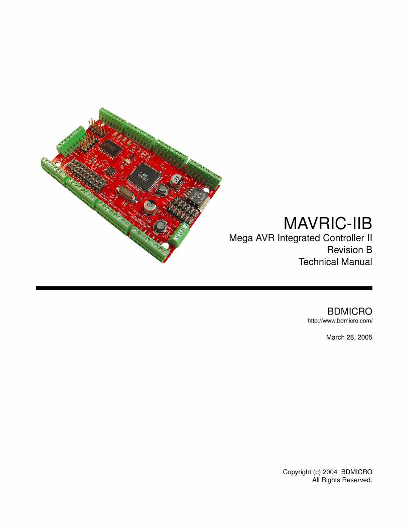
MAVRIC-IIBMega AVR Integrated Controller II
Revision BTechnical Manual
BDMICROhttp://www.bdmicro.com/
March 28, 2005
Copyright (c) 2004 BDMICROAll Rights Reserved.
MAVRIC-IIB • Technical Manual • March 28, 2005 Page 2 of 17
DISCLAIMER
BDMICRO products are designed and assembled with care and all assembled products must pass functional testingto ensure quality before they are shipped. However, our products are not rated for use in medical, life support, orsystems where failure could result in the loss of life or have serious life threatening or economic impact.
BDMICRO does not warrant merchantability for any purpose and shall not be liable for any direct, indirect, incidental,special, exemplary, or consequential damages of any kind, however incurred, through the use of our products.
BDMICRO • http://www.bdmicro.com/ /doc/mavric-ii.tex
MAVRIC-IIB • Technical Manual • March 28, 2005 Page 3 of 17
Contents
1 MAVRIC-IIB Layout 4
2 Power Supply Connections 6
3 In-System Programming and JTAG Debug Headers 7
4 Port Header Connections 8
4.1 I2C Connections . . . . . . . . . . . . . . . . . . . . . . . . . . . . . . . . . . . . . . . . . . . . . . . . 9
4.2 A/D Inputs and AREF Connection . . . . . . . . . . . . . . . . . . . . . . . . . . . . . . . . . . . . . . 9
4.3 PORTG3 and PORTG4 Connections . . . . . . . . . . . . . . . . . . . . . . . . . . . . . . . . . . . . . 10
5 Serial Communications Connections 10
6 DIP Switch Settings 11
7 Servo Headers 13
8 Fuse Bit Settings 14
9 Memory Expansion 14
10 Schematic Diagram 15
11 Mechanical Drawing 16
12 Soldering the MAVRIC-IIB Board 17
BDMICRO • http://www.bdmicro.com/ /doc/mavric-ii.tex
MAVRIC-IIB • Technical Manual • March 28, 2005 Page 4 of 17
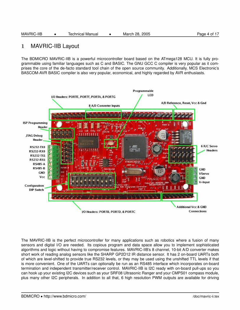
1 MAVRIC-IIB Layout
The BDMICRO MAVRIC-IIB is a powerful microcontroller board based on the ATmega128 MCU. It is fully pro-grammable using familiar languages such as C and BASIC. The GNU GCC C compiler is very popular as it com-prises the core of the de-facto standard tool chain of the open source community. Additionally, MCS Electronic’sBASCOM-AVR BASIC compiler is also very popular, economical, and highly regarded by AVR enthusiasts.
The MAVRIC-IIB is the perfect microcontroller for many applications such as robotics where a fusion of manysensors and digital I/O are needed. Its copious program and data space allow you to implement sophisticatedalgorithms and logic without having to compromise features. MAVRIC-IIB’s 8 channel, 10-bit A/D converter makesshort work of reading analog sensors like the SHARP GP2D12 IR distance sensor. It has 2 on-board UARTs bothof which are level-shifted to provide true RS232 levels, or they may be used using the unshifted TTL levels if thatis more convenient. One of the UARTs can optionally be run as an RS485 interface which incorporates on-boardtermination and independent transmitter/receiver control. MAVRIC-IIB is I2C ready with on-board pull-ups so youcan hook up your existing I2C devices such as your SRF08 Ultrasonic Ranger and your CMPS01 compass module,plus many other I2C peripherals. In addition to all that, 6 high resolution PWM outputs are available for driving
BDMICRO • http://www.bdmicro.com/ /doc/mavric-ii.tex
MAVRIC-IIB • Technical Manual • March 28, 2005 Page 5 of 17
servos and PWM motors with high precision. And with up to 51 digital I/O pins, it can handle even the most complexand demanding control tasks.
The MAVRIC-IIB also includes 6 R/C servo headers for controlling servos directly. An auxiliarly power input isprovided to power the servos seperately from the microcontroller electronics which protects the on-board electronicsfrom the high current drain and assocated brown-outs that can result from powering motors and electronics fromthe same power supply.
The on-board standard programming headers make development easy — 10-pin serial ISP header for connectingto your AVRISP or STK500, and also the standard 10-pin JTAG header for using your JTAGICE for programmingand single-step, source level debugging.
The MAVRIC-IIB incorporates an advanced, on-board, low-dropout voltage regulator and can be powered with aslittle as 5.5 Volts. Four mounting holes are provided for securely mounting your board, and with it’s small size of 2.2x 3.6 inches, you can mount it just about anywhere.
The capabilities of the ATmega128 MCU are numerous. Here are some of the highlights of the chip:
• 128K Flash memory (program space)
• 4K internal static RAM
• 4K EEPROM
• optional 64K external static RAM
• 8 channel analog to digital converter
• dual UARTs
• I2C interface
• up to 53 digital I/O pins
• JTAG interface for programming and debugging
• 2 8-bit timers, 1 16-bit timer
• 6 PWM channels
• Watchdog timer
For a more detailed look at the ATmega128, the best reference is the datasheet provided by the chip manufacturer,Atmel. The datasheet is available from Atmel in the form of a PDF file here:
http://www.atmel.com/dyn/resources/prod documents/doc2467.pdf
BDMICRO • http://www.bdmicro.com/ /doc/mavric-ii.tex
MAVRIC-IIB • Technical Manual • March 28, 2005 Page 6 of 17
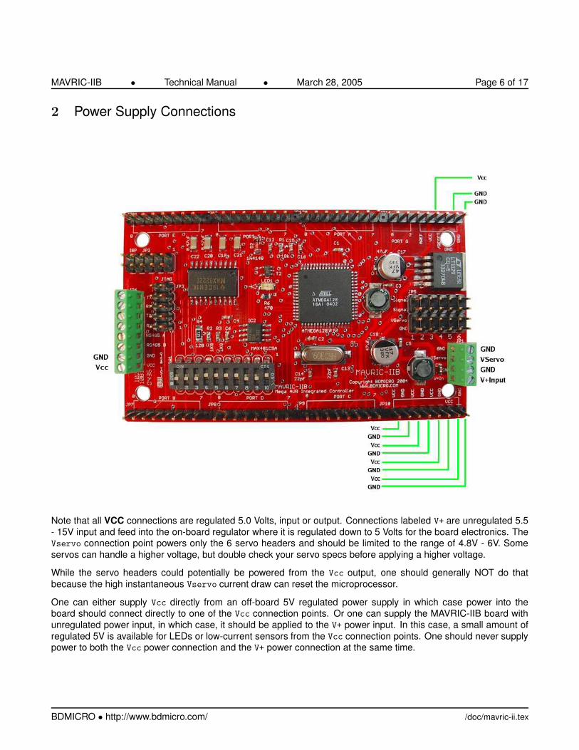
2 Power Supply Connections
Note that all VCC connections are regulated 5.0 Volts, input or output. Connections labeled V+ are unregulated 5.5- 15V input and feed into the on-board regulator where it is regulated down to 5 Volts for the board electronics. TheVservo connection point powers only the 6 servo headers and should be limited to the range of 4.8V - 6V. Someservos can handle a higher voltage, but double check your servo specs before applying a higher voltage.
While the servo headers could potentially be powered from the Vcc output, one should generally NOT do thatbecause the high instantaneous Vservo current draw can reset the microprocessor.
One can either supply Vcc directly from an off-board 5V regulated power supply in which case power into theboard should connect directly to one of the Vcc connection points. Or one can supply the MAVRIC-IIB board withunregulated power input, in which case, it should be applied to the V+ power input. In this case, a small amount ofregulated 5V is available for LEDs or low-current sensors from the Vcc connection points. One should never supplypower to both the Vcc power connection and the V+ power connection at the same time.
BDMICRO • http://www.bdmicro.com/ /doc/mavric-ii.tex
MAVRIC-IIB • Technical Manual • March 28, 2005 Page 7 of 17
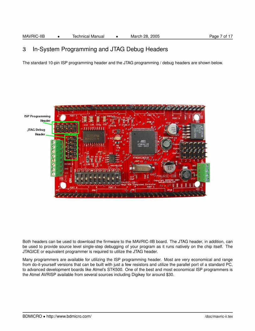
3 In-System Programming and JTAG Debug Headers
The standard 10-pin ISP programming header and the JTAG programming / debug headers are shown below.
Both headers can be used to download the firmware to the MAVRIC-IIB board. The JTAG header, in addition, canbe used to provide source level single-step debugging of your program as it runs natively on the chip itself. TheJTAGICE or equivalent programmer is required to utilize the JTAG header.
Many programmers are available for utilizing the ISP programming header. Most are very economical and rangefrom do-it-yourself versions that can be built with just a few resistors and utilize the parallel port of a standard PC,to advanced development boards like Atmel’s STK500. One of the best and most economical ISP programmers isthe Atmel AVRISP available from several sources including Digikey for around $30.
BDMICRO • http://www.bdmicro.com/ /doc/mavric-ii.tex
MAVRIC-IIB • Technical Manual • March 28, 2005 Page 8 of 17
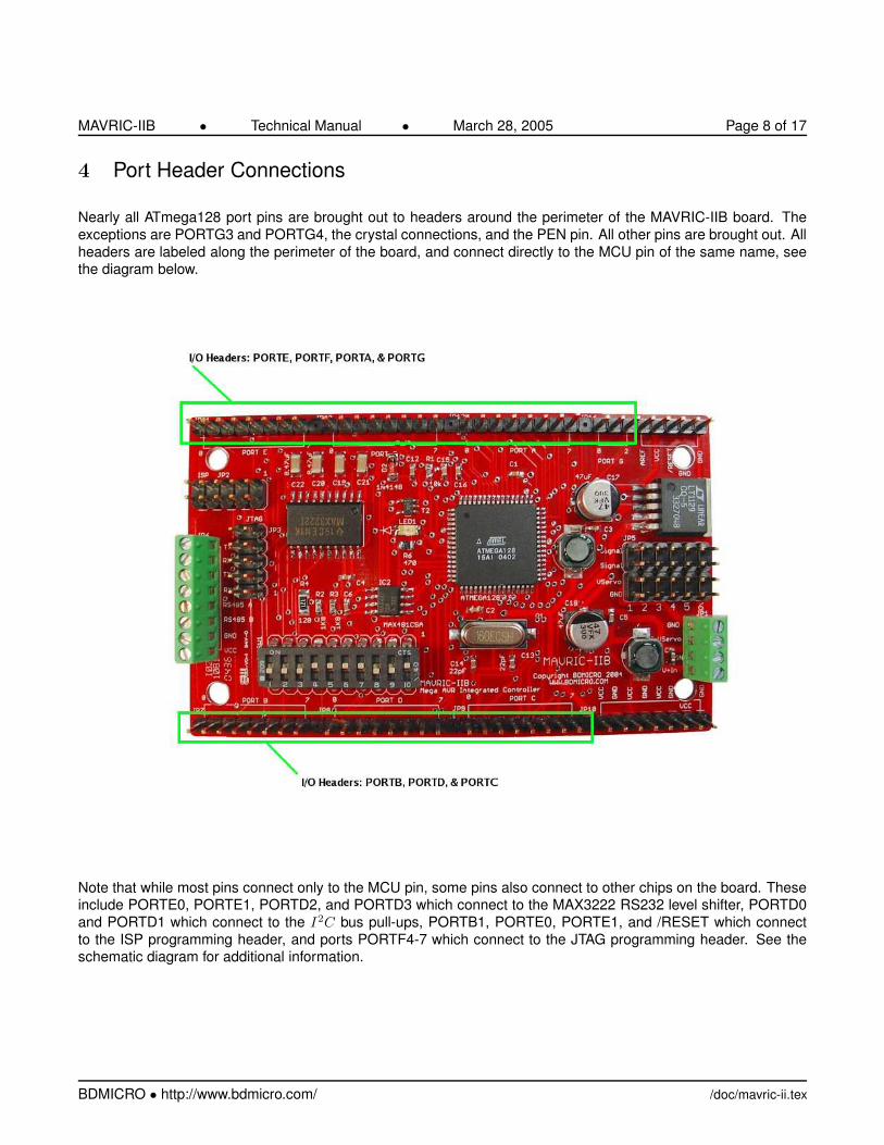
4 Port Header Connections
Nearly all ATmega128 port pins are brought out to headers around the perimeter of the MAVRIC-IIB board. Theexceptions are PORTG3 and PORTG4, the crystal connections, and the PEN pin. All other pins are brought out. Allheaders are labeled along the perimeter of the board, and connect directly to the MCU pin of the same name, seethe diagram below.
Note that while most pins connect only to the MCU pin, some pins also connect to other chips on the board. Theseinclude PORTE0, PORTE1, PORTD2, and PORTD3 which connect to the MAX3222 RS232 level shifter, PORTD0and PORTD1 which connect to the I2C bus pull-ups, PORTB1, PORTE0, PORTE1, and /RESET which connectto the ISP programming header, and ports PORTF4-7 which connect to the JTAG programming header. See theschematic diagram for additional information.
BDMICRO • http://www.bdmicro.com/ /doc/mavric-ii.tex
MAVRIC-IIB • Technical Manual • March 28, 2005 Page 9 of 17
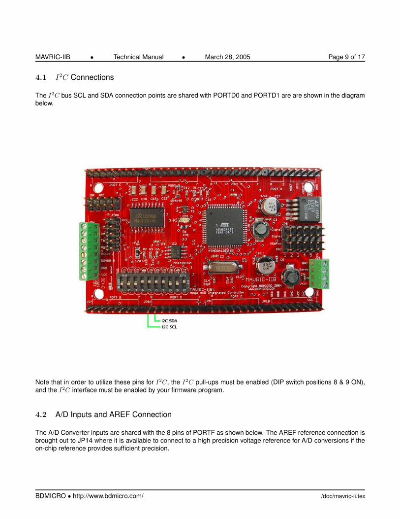
4.1 I2C Connections
The I2C bus SCL and SDA connection points are shared with PORTD0 and PORTD1 are are shown in the diagrambelow.
Note that in order to utilize these pins for I2C, the I2C pull-ups must be enabled (DIP switch positions 8 & 9 ON),and the I2C interface must be enabled by your firmware program.
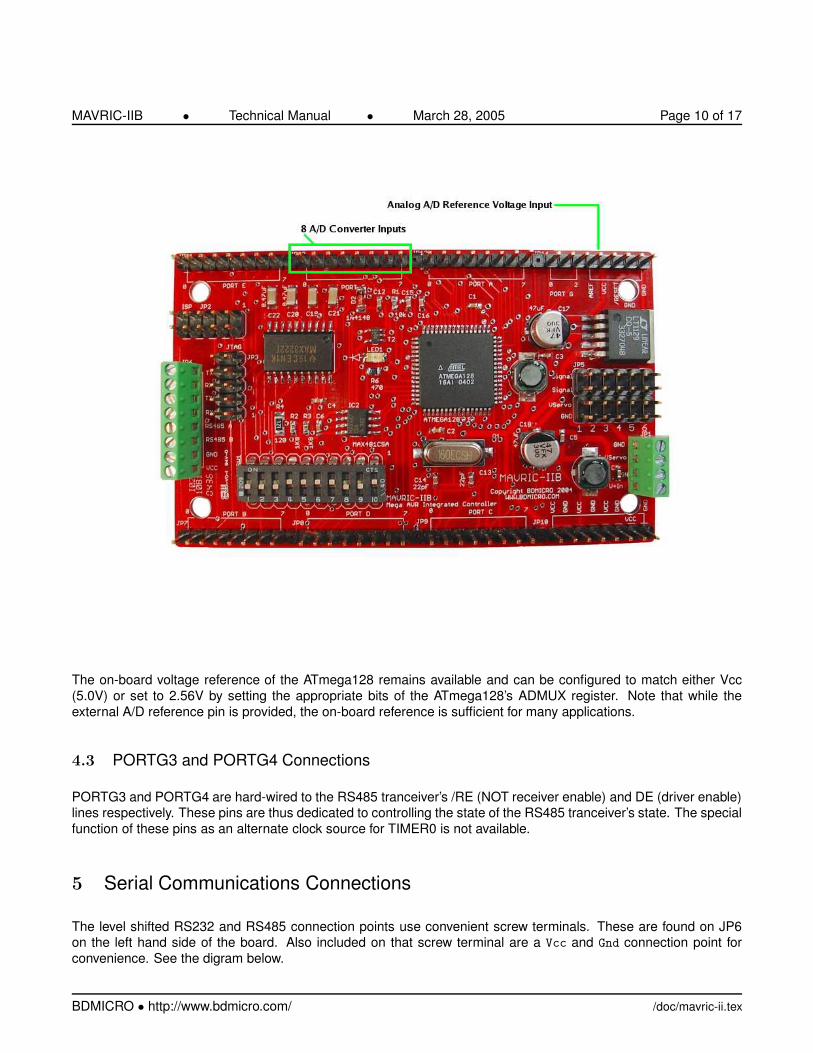
4.2 A/D Inputs and AREF Connection
The A/D Converter inputs are shared with the 8 pins of PORTF as shown below. The AREF reference connection isbrought out to JP14 where it is available to connect to a high precision voltage reference for A/D conversions if theon-chip reference provides sufficient precision.
BDMICRO • http://www.bdmicro.com/ /doc/mavric-ii.tex
MAVRIC-IIB • Technical Manual • March 28, 2005 Page 10 of 17
The on-board voltage reference of the ATmega128 remains available and can be configured to match either Vcc(5.0V) or set to 2.56V by setting the appropriate bits of the ATmega128’s ADMUX register. Note that while theexternal A/D reference pin is provided, the on-board reference is sufficient for many applications.
4.3 PORTG3 and PORTG4 Connections
PORTG3 and PORTG4 are hard-wired to the RS485 tranceiver’s /RE (NOT receiver enable) and DE (driver enable)lines respectively. These pins are thus dedicated to controlling the state of the RS485 tranceiver’s state. The specialfunction of these pins as an alternate clock source for TIMER0 is not available.
5 Serial Communications Connections
The level shifted RS232 and RS485 connection points use convenient screw terminals. These are found on JP6on the left hand side of the board. Also included on that screw terminal are a Vcc and Gnd connection point forconvenience. See the digram below.
BDMICRO • http://www.bdmicro.com/ /doc/mavric-ii.tex
MAVRIC-IIB • Technical Manual • March 28, 2005 Page 11 of 17
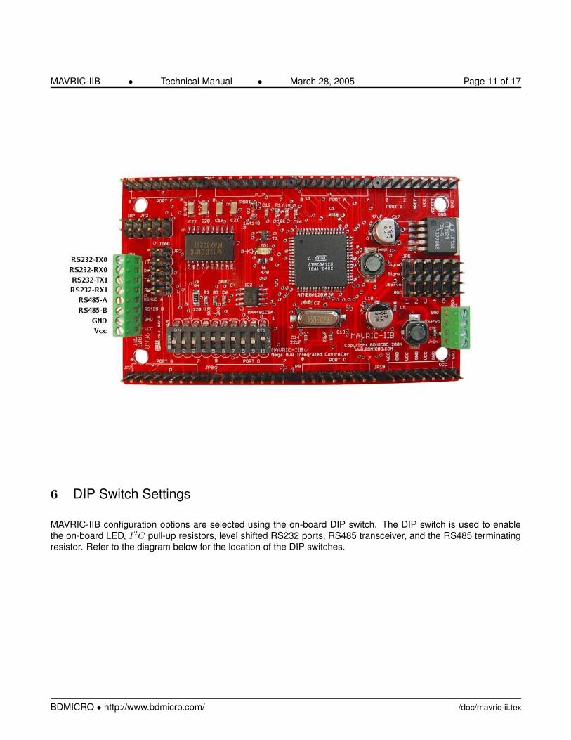
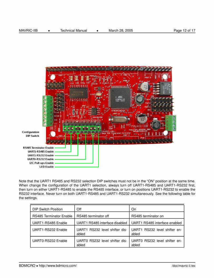
6 DIP Switch Settings
MAVRIC-IIB configuration options are selected using the on-board DIP switch. The DIP switch is used to enablethe on-board LED, I
2C pull-up resistors, level shifted RS232 ports, RS485 transceiver, and the RS485 terminating
resistor. Refer to the diagram below for the location of the DIP switches.
BDMICRO • http://www.bdmicro.com/ /doc/mavric-ii.tex
MAVRIC-IIB • Technical Manual • March 28, 2005 Page 12 of 17
Note that the UART1 RS485 and RS232 selection DIP switches must not be in the “ON” position at the same time.When change the configuration of the UART1 selection, always turn off UART1-RS485 and UART1-RS232 first,then turn on either UART1-RS485 to enable the RS485 interface, or turn on positions UART1-RS232 to enable theRS232 interface. Never turn on both UART1-RS485 and UART1-RS232 simultaneously. See the following table forthe settings.
DIP Switch Position Off On
RS485 Terminator Enable RS485 terminator off RS485 terminator on
UART1-RS485 Enable UART1 RS485 interface disabled UART1 RS485 interface enabled
UART1-RS232 Enable UART1 RS232 level shifter dis-abled
UART1 RS232 level shifter en-abled
UART0-RS232 Enable UART0 RS232 level shifter dis-abled
UART0 RS232 level shifter en-abled
BDMICRO • http://www.bdmicro.com/ /doc/mavric-ii.tex
MAVRIC-IIB • Technical Manual • March 28, 2005 Page 13 of 17
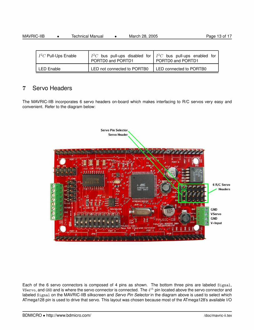
I2C Pull-Ups Enable I2C bus pull-ups disabled forPORTD0 and PORTD1
I2C bus pull-ups enabled forPORTD0 and PORTD1
LED Enable LED not connected to PORTB0 LED connected to PORTB0
7 Servo Headers
The MAVRIC-IIB incorporates 6 servo headers on-board which makes interfacing to R/C servos very easy andconvenient. Refer to the diagram below:
Each of the 6 servo connectors is composed of 4 pins as shown. The bottom three pins are labeled Signal,VServo, and GND and is where the servo connector is connected. The 4
th pin located above the servo connector andlabeled Signal on the MAVRIC-IIB silkscreen and Servo Pin Selector in the diagram above is used to select whichATmega128 pin is used to drive that servo. This layout was chosen because most of the ATmega128’s available I/O
BDMICRO • http://www.bdmicro.com/ /doc/mavric-ii.tex
MAVRIC-IIB • Technical Manual • March 28, 2005 Page 14 of 17
pins are shared with at least one of the chip’s special peripheral features. This layout allows you to choose whichof the ATmega128 pin(s) are used for driving servos, as opposed to hard-wiring the servo signal to certain pins,which would otherwise make the special peripheral feature of that pin unavailable to your application. Thus, youshould wire the Servo Pin Selector pin for each servo connector to the ATmega128 pin of your choosing for drivingthat servo. In this way, you have greater flexibility to allocate the ATmega128’s on-chip resources to precisely matchyour application’s needs.
8 Fuse Bit Settings
Atmel AVR processors incorporate fuse bits which control various functions of the chip and persist even across achip erase. By default, Atmel ships the ATmega128 with several fuse bits already programmed by default. Notably,the M103C fuse bit (ATmega103 compatibility mode) is enabled, as well as JTAGEN which enables the JTAGdebugging lines of PORT F. Also, by default, the internal clock source is selected to run the processor at 1 MHz.
If you ordered a Kit, your ATmega128 processor’s fuse bits are all at their default values and will need to be changedto run on the MAVRIC-IIB board at 16 MHz. For 16 MHz operation, you will need to program the CKOPT fuse bit(set to ’0’). The clock selection lines will need to be modified as well: unprogram CKSEL3, CKSEL2, CKSEL1,and CKSEL0 (set to ’1’). Also recommended when using the external crystal is to set SUT1 and SUT0 to ’1’(unprogrammed). This setting is for slow rising power which may be necessary depending on your power supply.Additionally, you will need to unprogram the M103C fuse bit (set to ’1’) if you are compiling your code to run on anATmega128 (as opposed to an ATmega103).
If you ordered an assembled and tested board, these fuse bits are already set appropriately to run at 16 MHz, andthe M103C fuse bit has been unprogrammed.
One other note with regard to fuse bits — the JTAG interface uses the upper nibble of PORT F, and the JTAGENfuse bit is programmed by default. Since the JTAG interface supersedes all other functions of the PORT F lines,their other functions are not available while the JTAGEN fuse bit is programmed. Thus, if you are not using a JTAGprogrammer/debugger, you may wish to unprogram the JTAGEN fuse bit. We leave the JTAGEN fuse bit in its defaultprogrammed state since the recipient of the board may only have a JTAG programmer/debugger. If JTAGEN wasunprogrammed, those with JTAG programmers would have to find another type of programmer (serial or parallel) inorder to change the state of the JTAGEN bit, just so they could begin working on the board.
For a description of all the fuse bits, see pages 286 and 287 of the ATmega128 data sheet available from Atmel’sweb site (http://www.atmel.com/).
9 Memory Expansion
The MAVRIC-IIB board has 4K of internal static RAM via the ATmega128 processor. While 4K of SRAM is con-sidered large for a microcontroller, some applications are memory intensive and require more. For this purpose,BDMICRO offers the MAVRIC-II-RE product, a RAM Expansion card that can be plugged in over the right half ofyour MAVRIC-IIB board. The MAVRIC-II-RE expands the memory capacity to 128K of RAM. In order to use theMAVRIC-II-RE, pin headers must be installed in JP9, JP10, JP13, and JP14. The MAVRIC-II-RE is available on-linefrom BDMICRO at http://www.bdmicro.com/.
BDMICRO • http://www.bdmicro.com/ /doc/mavric-ii.tex
MAVRIC-IIB • Technical Manual • March 28, 2005 Page 15 of 17
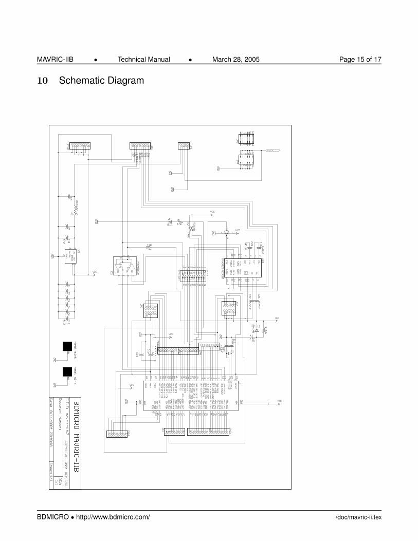
10 Schematic Diagram
BDMICRO • http://www.bdmicro.com/ /doc/mavric-ii.tex
MAVRIC-IIB • Technical Manual • March 28, 2005 Page 16 of 17
11 Mechanical Drawing
2.0 inches
3.4 inches
0.2 inches
0.3
inch
es
0.2 inches
0.1 inches
0.12
5 in
ches
2.2
inch
es
3.6 inches
PORT E PORT F PORT A
PORT CPORT DPORT B GN
D
VC
C
GN
D
GN
D
GN
D
RE
SE
T0 0 07 7 7
0 0 07 7 7
BDMICROMAVRIC-IIB
Mega AVR Integrated ControllerTOP VIEW
http://www.bdmicro.com/
0.1 inches
GN
D
VC
C
GN
D
VC
C
0PORT G
2
0.1 inches
VCC
AR
EF
VC
C
BDMICRO • http://www.bdmicro.com/ /doc/mavric-ii.tex
MAVRIC-IIB • Technical Manual • March 28, 2005 Page 17 of 17
12 Soldering the MAVRIC-IIB Board
If you purchased a bare board or a kit with a bare board, you will be soldering the components on the board. Asmall diameter solder such as 0.015 inches works well for the small surface mount parts. A temperature controllediron also makes the job easier. If your vision is not the best (like mine), I’ve found that a magnifying visor helps agreat deal. A short tutorial with some photos is available on the web site at http://www.bdmicro.com/smt/. Themain points to remember are:
• Use your solder sparingly, it takes only a tiny amount to make a good connection.
• Don’t use your soldering iron directly to melt the solder. Doing so causes the solder to bead up due to surfacetension on the iron and then release in a big drop across the pins. This results in too much solder and causesbridging, shorting adjacent pins together.
Instead, use your iron to heat the pin, which then melts the pad underneath the pin. At this point, touch your0.015 inch solder to the base of the pin. It should melt very quickly, consuming only one or two millimeters ofsolder, and flow onto the pin and around the pad. Remove the solder quickly.
• Make sure your iron is hot — about 630 degrees F seems to be about right. It needs to be hot enough to meltthe solder indirectly, but not so hot that it damages the part.
• While not absolutely required, a good temperature-controlled soldering iron can make the process go mucheasier than with the standard soldering pencil type irons. If you plan to do much soldering, especially thesmaller parts, it would be well worth your investment to acquire one. In fact, good deals can usually be foundon on-line auction sites such as E-Bay.
The order in which you solder the parts can make the soldering easier. In general, I solder the parts based onsize with the smaller parts first followed by successively larger parts. Thus, I install the surface mount capacitors,resistors, and diodes first, followed by the ICs, the larger surface mount caps and inductor, crystals, and finally thepin headers.
A good technique that I’ve found for soldering on even the tiniest of surface mount parts is this simple procedure,especially for tiny resistors and capacitors:
• First, prepare one pad by heating it with the tip of your soldering iron and flowing a bit of solder onto the pad.This will make a raised solder surface. Only do one pad at this point, not both.
• Use a pair of fine tweezers to move the part into position.
• Use the tip of your fingernail to hold the part in place, then re-apply heat to the raised solder area. The solderwill liquify and the part will sink into position and be held firmly in place by the solder.
• Now move to the unsoldered side and apply a bit of solder to complete the connection.
• Finally, if necessary, return to the first side of the part, and re-apply a tiny bit of solder to ensure a goodconnection there.
This technique is described on the web site with photos for clarification. See http://www.bdmicro.com/smt/.
You can save time by first preparing one pad of each part by applying solder, then attach one side of all the parts,then solder the other side of all the parts, etc, instead of performing all the steps for a part before moving to the nextone.
BDMICRO • http://www.bdmicro.com/ /doc/mavric-ii.tex
![Bascom AVR Programming [Basic]](https://static.fdocuments.us/doc/165x107/544a8b55b1af9f0f568b4d6d/bascom-avr-programming-basic.jpg)