MediNano6 - Centre national de la recherche scientifiqueinl.cnrs.fr/medinano6/Medinano-6...
67
MediNano6 6th Mediterranean Conference on Nano-Photonics MediNano-6 30-31 October, 2013, Lyon, France
Transcript of MediNano6 - Centre national de la recherche scientifiqueinl.cnrs.fr/medinano6/Medinano-6...

MediNano6
6th Mediterranean Conference on Nano-Photonics MediNano-6 30-31 October, 2013, Lyon, France

MediNano6
Welcome to Medinano-6 Nano-photonics is one of the most appealing fields having large variety of academic as well
industrial applications. MediNano is an international gathering inviting participants from research institutes and industries in countries surrounding the Mediterranean Sea to present their most recent results as well as review of concepts in various topics related to nano-photonics. Following the successful gathering of MediNano-1, 2, 3, 4 and 5 which were organized in Istanbul (Turkey) in 2008, Athens (Greece) in 2009, in Belgrade (Serbia) in 2010, Rome (Italy) in 2011 and Barcelona (Spain) in 2012, the meeting of Medinano-6 will be held in the Lyon at INL- the Lyon Nanotechnology Institute , France. The previous meetings had more than 100 participants on average from more than 25 countries (mostly but not only Mediterranean) presented the highlights of their recent achievements in the field of nano-photonics.
Original manuscripts are solicited in research areas related to nano-photonics, including but not limited to the following:
Metamaterials Photonic Crystal Fibers Sensing and Imaging Computational nano photonics Non linear nano optics Nano and micro manipulations Nano/ micro photonic devices • Silicon photonics and plasmonics
Local Organization Taha BENYATTOU and Xavier LETARTRE, INL, Lyon, France Nathalie Destouches Castagna, LHC, St Etienne, France François Royer, St Etienne, LT2C, St Etienne, France
Organizing Committee Zeev Zalevsky, Bar Ilan University, Ramat Gan, Israel Ekmel Ozbay, Bilkent University, Ankara,Turkey Alper Kiraz, Koç University, Koç, Turkey Turkey Georgios Kakarantzas, National Hellenic Research Foundation, Greece Maria Kafesaki, Foundation for Research and Technology Hellas (FORTH),Greece Romain Quidant, ICFO ·The Institute of Photonic Sciences, Barcelona, Spain Niek van Hulst, ICFO ·The Institute of Photonic Sciences, Barcelona, Spain Zoran Jaksic, University of Belgrade, Serbia Philippe Lalanne, CNRS, Universite Paris-Sud, Campus Polytechnique, France Taha Benyattou, INL, Lyon, France Xavier Letartre, INL, Lyon, France

October 30
8h45 Welcome to MediNano6 @INL INSA, T. Benyattou & Z. Zalevski SESSION 1 Chairman: E. Ozbay, Bilkent University, Ankara,Turkey 9h-9h45 Plenary talk: Hybrid Light-Matter States – Potential for Molecular and Material
Sciences Thomas Ebbesen, Nanostructures Laboratory ,ISIS, Strasbourg, FRANCE
9h45-10h15 T1 Invited: Surface plasmon lasing in metal hole arrays Martin van Exter, Huygens Laboratory, Leiden University, The Netherlands
10h15-10h35 T2 Singular analysis of Fano resonances in plasmonic nanostructures Victor Grigoriev, Institut Fresnel, UMR 7249, Marseille, France
10h35-11h Coffee Break SESSION 2 Chairman: T. Benyattou, INL, LYON,France 11h-11h30 T3 Invited: Diamond – Engineer’s Best Friend
Marko Loncar, Harvard University, USA 11h30-12h T4 Invited : Nano-Plasmonic Biosensors and Photodetectors
Ekmel Ozbay, Nanotechnology Research Center, Bilkent University,Turkey 12h-12h20 T5 Reconfigurable photonic structures based on surface enhanced Raman scattering
in nanorods, Zeev Zalevsky, Bar-Ilan University,Israel 12h20-12h40 T6 Nanostencil Lithography for Flexible Plasmonics and Vibrational Biospectroscopy
Serap Aksu,Boston University Photonics Center,USA 12h40-13h40 Lunch 13h40-15h30
Poster session
SESSION 3 Chairman: Hatice Altug, EPFL, Switzerland 15h25-15h30 Presentation of the C’Nano network , Christian Seassal, INL,LYON , FRANCE 15h30-16h T7 Invited : Enhanced Inhibited Coupling in hypocycloid core Kagome HC-PCF and
milli-Joule Energy Ultra-Short pulse guidance and compression Frédéric Gérôme, XLIM,CNRS, France
16h-16h30 T8 Invited : Novel Applications of Terahertz and Infrared Metamaterials: From Energy Harvesting to Imaging, Willie Padilla, Boston College, USA
16h30-16h50 T9 Second Harmonic Generation from Realistic Plasmonic Nanoantennas and Fano Metamolecules, Jeremy Butet, NAM, EPFL, 1015, Lausanne, Switzerland
16h50-17h10 T10 Plasmonic Excitations in Bi2Se3 Topological Insulator Odeta Limaj, EPFL,Lausanne, Switzerland
17h10-17h30 Coffee break SESSION 4 Chairman: Z. Zalevsky, Bar Ilan University, Ramat Gan, Israel 17h30-18h T11 Invited : Photonic crystals: key nanostructures for light trapping and advanced
solar cells Christian Seassal, INL,LYON , FRANCE 18h-18h30 T12 Invited : Plasmons in low-dimensional structures
Javier Garcia de Abajo, CSIC, Madrid, Spain 18h30-18h50 T13 Control of metallic nanostructures within a silica layer by atomic force
microscopy, S. Bakhti,LHC, St. Etienne,FRANCE 18h50-19h10 T14 Effective Medium Approach to Response of Adsorption-Based Nanoplasmonic
Chemical Sensors, Zoran Jakšić, Center of Microelectronic Technologies, Serbia 20h Gala Diner : Restaurant de Fourvière

October 31 SESSION 5 Chairman: Z. Jakšić , University of Belgrade, Serbia 8h-8h30 T15 Invited : A New Way to Tame Light: Electrically controlled resistive switching assisted
active broadband optical tenability, Ali Kemal Okyay, Bilkent University, Ankara, TURKEY 8h30-9h T16 Invited :Recent Improvements in Plasmonic Biosensing Techniques
Ibrahim Abdulhalim, BGU, Israel 9h-9h20 T17 SiNx thin films as sensitive screens for bio-imaging
Tetyana Nishiporuk,INL,Lyon,France 9h20-9h40 T18 Biosensing of living cells using infra-red surface plasmons
Dan Davidov, The Racah Institute of Physics, Jerusalem, Israel 9h40-10h T19 Optofluidic chip with integrated photonic tweezers
Christophe PIN, SiNaPS lab./SP2M, Grenoble, France 10h-10h20 Coffee Break SESSION 6 Chairman: X. Letartre, INL, LYON ,France 10h20-10h50 T20 Invited : Nanophotonic periodic structures with reduced symmetry
Hamza Kurt, TOBB University, Ankara, TURKEY 10h50-11h20 T21 Invited : Linear and nonlinear optical responses of single bi-metallic nanoparticle
Fabrice Vallée, ILM, LYON, FRANCE 11h20-11h50 T22 Invited : Locally Resonant Metamaterials: Focusing, Imaging and Manipulating Waves
at the Deep Subwavelength Scale, Geoffroy Lerosey, Institut Langevin, France 11h50-12h10 T23 Taming blackbody radiation with surface waves: near field
Jean Jacques Greffet, Laboratoire Charles Fabry, Institut d'Optique,France 12h10-13h30
Lunch
SESSION 7 Chairman: Javier Garcia de Abajo, ICFO Barcelona, Spain 13h30-14h T24 Invited:Time-Resolved and Ultra-Sensitive Vibrational Biospectroscopy with Mid-
Infrared Plasmonics, Hatice Altug, Boston Univ. and EPFL in Switzerland 14h-14h30 T25 Invited : Terahertz and Infrared Plasmonics and Metasurfaces
Tahsin Akalin, University of Lille, France 14h30-15h T26 Invited : Instabilities and Rogue Waves in Nonlinear Fiber Optics
Pierre-Ambroise Lacourt, FEMTO ST,Besançon, France 15h-15h20 T27 Plasmon-soliton coupling: design of realistic structures
Gilles RENVERSEZ, Institut Fresnel, Marseille, France 15h20-15h40 Coffee Break SESSION 8 Chairman: I. Abdulhalim, Ben-Gurion University, Israel 15h40-16h10 T28 Invited: A feasibility study for controlling self-organize production of plasmonic
enhancement interfaces for solar cells , Alpan Bek, Middle East Technical University, Turkey
16h10-16h40 T29 Invited: “Enhancing light matter interactions using nanoscale integration of silicon, metals and vapors”, Uriel Levy, HUJI, Israel
16h40-17h10 T30 Invited: Microsphere resonators integrated inside microstructured optical fibers: studies and optimization, Kyriaki KOSMA,IESL,FORTH,GREECE
17h10-17h30 T31 Simple Evanescent Field Sensor for NIR Spectroscopy Alina Karabchevsky,Optoelectronics Research Centre, Southampton, UK
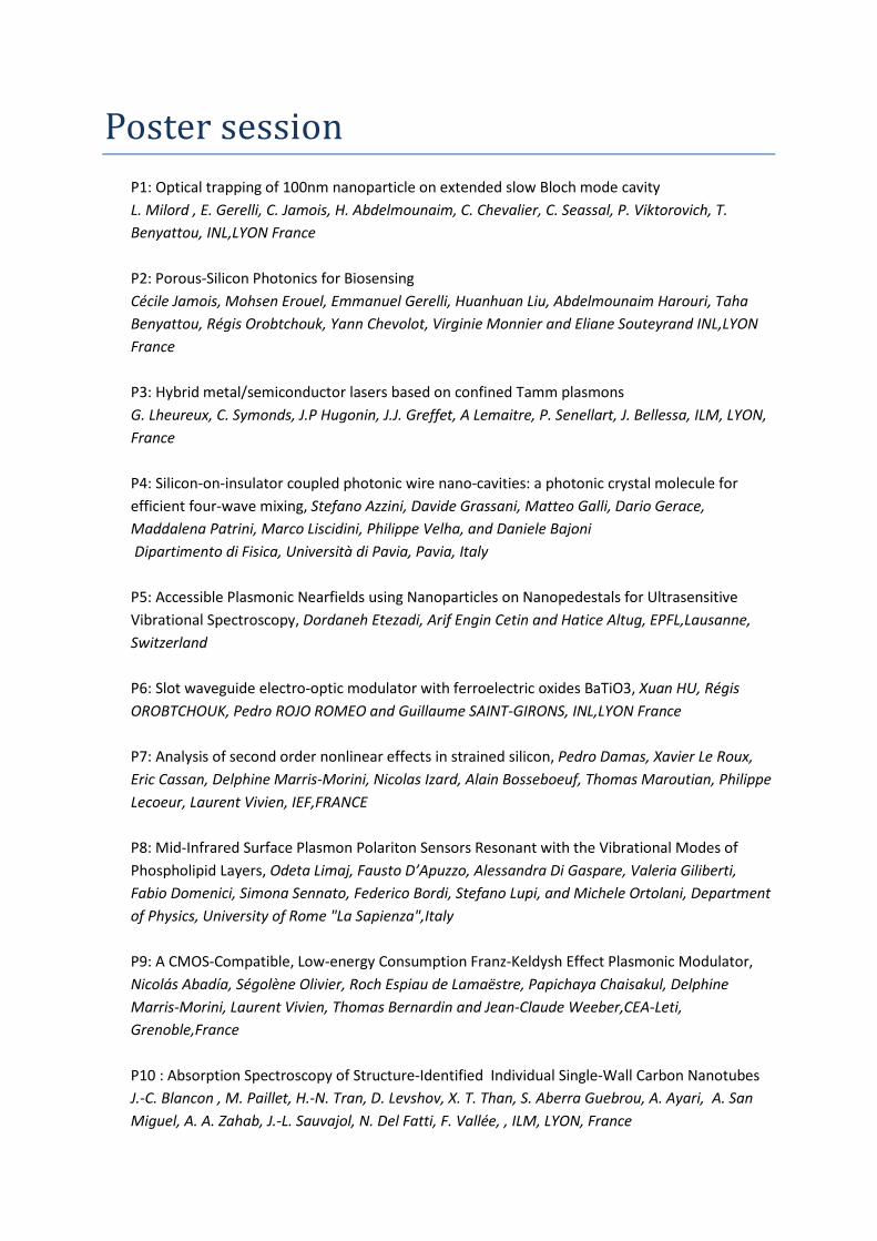
Poster session P1: Optical trapping of 100nm nanoparticle on extended slow Bloch mode cavity L. Milord , E. Gerelli, C. Jamois, H. Abdelmounaim, C. Chevalier, C. Seassal, P. Viktorovich, T. Benyattou, INL,LYON France P2: Porous-Silicon Photonics for Biosensing Cécile Jamois, Mohsen Erouel, Emmanuel Gerelli, Huanhuan Liu, Abdelmounaim Harouri, Taha Benyattou, Régis Orobtchouk, Yann Chevolot, Virginie Monnier and Eliane Souteyrand INL,LYON France P3: Hybrid metal/semiconductor lasers based on confined Tamm plasmons G. Lheureux, C. Symonds, J.P Hugonin, J.J. Greffet, A Lemaitre, P. Senellart, J. Bellessa, ILM, LYON, France P4: Silicon-on-insulator coupled photonic wire nano-cavities: a photonic crystal molecule for efficient four-wave mixing, Stefano Azzini, Davide Grassani, Matteo Galli, Dario Gerace, Maddalena Patrini, Marco Liscidini, Philippe Velha, and Daniele Bajoni Dipartimento di Fisica, Università di Pavia, Pavia, Italy P5: Accessible Plasmonic Nearfields using Nanoparticles on Nanopedestals for Ultrasensitive Vibrational Spectroscopy, Dordaneh Etezadi, Arif Engin Cetin and Hatice Altug, EPFL,Lausanne, Switzerland P6: Slot waveguide electro-optic modulator with ferroelectric oxides BaTiO3, Xuan HU, Régis OROBTCHOUK, Pedro ROJO ROMEO and Guillaume SAINT-GIRONS, INL,LYON France P7: Analysis of second order nonlinear effects in strained silicon, Pedro Damas, Xavier Le Roux, Eric Cassan, Delphine Marris-Morini, Nicolas Izard, Alain Bosseboeuf, Thomas Maroutian, Philippe Lecoeur, Laurent Vivien, IEF,FRANCE P8: Mid-Infrared Surface Plasmon Polariton Sensors Resonant with the Vibrational Modes of Phospholipid Layers, Odeta Limaj, Fausto D’Apuzzo, Alessandra Di Gaspare, Valeria Giliberti, Fabio Domenici, Simona Sennato, Federico Bordi, Stefano Lupi, and Michele Ortolani, Department of Physics, University of Rome "La Sapienza",Italy P9: A CMOS-Compatible, Low-energy Consumption Franz-Keldysh Effect Plasmonic Modulator, Nicolás Abadía, Ségolène Olivier, Roch Espiau de Lamaëstre, Papichaya Chaisakul, Delphine Marris-Morini, Laurent Vivien, Thomas Bernardin and Jean-Claude Weeber,CEA-Leti, Grenoble,France P10 : Absorption Spectroscopy of Structure-Identified Individual Single-Wall Carbon Nanotubes J.-C. Blancon , M. Paillet, H.-N. Tran, D. Levshov, X. T. Than, S. Aberra Guebrou, A. Ayari, A. San Miguel, A. A. Zahab, J.-L. Sauvajol, N. Del Fatti, F. Vallée, , ILM, LYON, France

P11: Handheld and Portable Plasmonic Biosensors for Field Settings Arif Cetin and Hatice Altug, EPFL,Lausanne, Switzerland P12: Angulo-spectral plasmonic properties of nano-micro-structured sensing substrates, Maha Chamtouri, Mitradeep Sarkar, Alexandra Sereda, Mondher Besbes, Anne-Lise Coutrot, Julien Moreau and Michael Canva, LCFIO,France P13: Fabrication and characterization of ultra-short lithium niobate photonic crystals with giant aspect ratios, C. Guyot, G. Ulliac, J. Dahdah, W. Qiu, M.-P. Bernal, F. Baida and N. Courjal, Institut FEMTO-ST,France P14: Analysis of tunable one-way terahertz surface-magnetoplasmonic InSb waveguides, P. Kwiecien, I. Richter, V. Kuzmiak, J. Čtyroký, Czech Technical University in Prague, Faculty of Nuclear Sciences and Physical Engineering, Czech Republic P15: Bloch Surface Waves Polaritons Pirotta S., Dacarro G., Patrini M., Galli M., Guizzetti G., Liscidini M., Canazza G., Comoretto D., Bajoni D., Department of Physics, Università degli Studi di Pavia,Italy P16: Pulsed Laser Deposition for research of innovative phosphor nanostructure made from Al and Ag, N. Abdellaoui, A. Pereira, G. Colas des Francs, A. Berthelot, B. Moine and A. Pillonnet, ILM, LYON, France P17: Complex photonic crystal structures to enhance optical light trapping in 2nd generation solar cells, L. Lalouat, R. Peretti, X. Meng, G. Gomard, C. Seassal, E. Drouard, INL, Lyon, France P18: Plasmonic slot waveguide couplers - comparison of linear and nonlinear regimes J. Petráček, P. Kwiecien, I. Richter, CTU in Prague, Czech Republic P19: InAs quantum dots in silicon by ion implantation M.A. Sortica, B. Canut, J.F. Dias, N. Chauvin, P.L. Grande, O. Marty , INL, Lyon, France P20: III-V nanowires based optical microsources coupled to a silicon waveguide, Z. Lin, M. Gendry, X. Letartre, INL, Lyon, France P21: Optical Lookup Table: a reconfigurable WDM nanophotonic computing architecture using microring resonators, Zhen Li, Christelle Monat, Sébastien Le Beux, Ian O’Connor, Xavier Letartre, INL, Lyon, France P22: Photonic crystal waveguides fabricated on the hydrogenated amorphous silicon material platform, L. Carletti, C. Grillet, R. Orobtchouk, T. Benyattou, P. Rojo-Romeo, X. Letartre, J.M. Fedeli and C. Monat, INL, Lyon, France

P23 : Analytical approach to extract the characteristics of plasmon resonance modes from the field scattered by metallic particles, S. Bakhti, A.V. Tishchenko, N. Destouches, LHC, St. Etienne,FRANCE P24: Transformation Optics with Cylindrical Symmetry and Lossy Media: An Analytical Approach M. Dalarsson, M. Norgrena and Z. Jakšić, Center of Microelectronic Technologies, Serbia P25 Nanoparticle-Enhanced Chemiluminescence in Micro-Flow Injection Analysis A. Mosayyebi, A. Karabchevsky and J. S. Wilkinson, Optoelectronics Research Centre, Southampton, UK P26 From a plasmonic vortex to a singular beam Y. Gorodetski, A. Drezet, C. Genet, and T. W. Ebbesen, Nanostructures Laboratory ,ISIS, Strasbourg, FRANCE P27 Photonic/Plasmonic coupling : A way towards higher performance sensors Huanhuan LIU, Emmanuel Gerelli, Mohsen Erouel, Abdelmounaim Harouri, Laurent Milord, Taha Benyattou, Régis Orobtchouk, Ali Belarouci, Xavier Letartre, Cécile Jamois,INL,LYON P28 Photon Cages R. Artinyan, A. Benamrouche, C. Belacel, A. Berthelot, A.M. Jurdyc, P. Rojo-Romeo, G. Grenet, A. Danescu, P. Regreny, J.L. Leclercq, X. Letartre, S. Callard, INL,LYON

Abstract booklet
Plenary talk
Hybrid Light-Matter States – Potential for Molecular and Material Sciences Thomas W. Ebbesen, ISIS, University of Strasbourg & CNRS Abstract: Strong coupling of light and matter can give rise to a multitude of exciting physical effects through the formation of hybrid states. Organic molecules have been increasingly used for the study of strong coupling since their large transition dipole moment permits the observation of vacuum Rabi splitting approaching 1 eV at room temperature. Such large modifications in the energy levels have significant implications for molecular and material sciences. Our recent research on this topic will be presented.
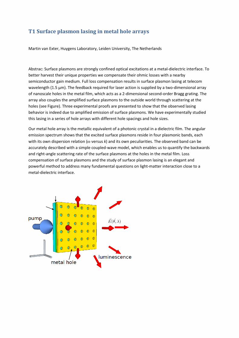
T1 Surface plasmon lasing in metal hole arrays
Martin van Exter, Huygens Laboratory, Leiden University, The Netherlands
Abstrac: Surface plasmons are strongly confined optical excitations at a metal-dielectric interface. To better harvest their unique properties we compensate their ohmic losses with a nearby semiconductor gain medium. Full loss compensation results in surface plasmon lasing at telecom wavelength (1.5 µm). The feedback required for laser action is supplied by a two-dimensional array of nanoscale holes in the metal film, which acts as a 2-dimensional second-order Bragg grating. The array also couples the amplified surface plasmons to the outside world through scattering at the holes (see Figure). Three experimental proofs are presented to show that the observed lasing behavior is indeed due to amplified emission of surface plasmons. We have experimentally studied this lasing in a series of hole arrays with different hole spacings and hole sizes.
Our metal hole array is the metallic equivalent of a photonic crystal in a dielectric film. The angular emission spectrum shows that the excited surface plasmons reside in four plasmonic bands, each with its own dispersion relation (ω versus k) and its own peculiarities. The observed band can be accurately described with a simple coupled-wave model, which enables us to quantify the backwards and right-angle scattering rate of the surface plasmons at the holes in the metal film. Loss compensation of surface plasmons and the study of surface plasmon lasing is an elegant and powerful method to address many fundamental questions on light-matter interaction close to a metal-dielectric interface.

T2 Singular analysis of Fano resonances in plasmonic nanostructures
V. Grigoriev*, S. Varault, G. Boudarham, B. Stout, J. Wenger and N. Bonod
CNRS, Aix Marseille Université, Centrale Marseille, Institut Fresnel, UMR 7249, 13013
Marseille, France
* Email: [email protected]
Plasmonic nanostructures offer a unique ability to engineer the optical properties at the scale which is smaller than the wavelength of light [1]. They are often fabricated as metal slabs periodically patterned with holes or as arrays of scatterers periodically arranged on a surface. The profile of the scatterers can be made in the form of split-ring resonators or various dolmen-like structures to control the coupling between different modes and to observe such effects as Fano interference, electromagnetically induced transparency and absorption [2]. In this work, it is proposed to analyze the scattering properties of plasmonic nanostructures in terms of perfectly emitting and absorbing modes [3]. These modes can be considered as point-like singularities in the domain of complex frequencies, where the reflection coefficient either goes to infinity (emission) or turns into zero (absorption). It is shown that the frequencies of these modes determine the shape of the reflection and transmission spectra in the same way as the positions of point-like charges determine the electric field around them. The charges can be of negative (emission) and positive (absorption) sign, but their absolute value is fixed, and they always appear in pairs. It is highly remarkable that only a few singular points are sufficient to reproduce the scattering spectra of plasmonic nanostructures over broad intervals of frequencies. Moreover, the analogy with electrostatics helps to develop a visual interpretation for many resonant effects which occur due to overlapping resonances so that the analysis of the interplay among them can be simplified significantly. As an example, the effect of Fano interference is considered which creates resonances of an asymmetric shape.
References [1] S. Enoch and N. Bonod, Plasmonics: From Basics to Advanced Topics (Springer, Berlin,
2012).
[2] M. Rahmani, B. Lukʼyanchuk, and M. Hong, Laser Photon. Rev. 7, 329 (2013).
[3] V. Grigoriev, A. Tahri, S. Varault, B. Rolly, B. Stout, J. Wenger, and N. Bonod, Phys. Rev. A 88, 011803(R) (2013).
r r 1 2
Fig. 1. An array of dolmen-like structures. The reflection spectrum for normal incidence, and its decomposition into perfectly emitting ω− and absorbing ω+ modes. The field profiles of quadrupolar ω− and dipolar ω− modes.

T3 Diamond – Engineer’s Best Friend! Marko Lončar
School of Engineering and Applied Science, Harvard University, Cambridge, MA 02138, USA [email protected], http://nano-optics.seas.harvard.edu
Abstract: Diamond possesses remarkable physical and chemical properties, and in many ways is the ultimate engineering material - “the engineer’s best friend!” For example, it has high mechanical hardness and large Young’s modulus, and is one of the best thermal conductors. Optically, diamond is transparent from the ultra-violet to infra-red, has a high refractive index (n = 2.4), strong optical nonlinearity and a wide variety of light-emitting defects. Finally, it is biocompatible and chemically inert, suitable for operation in harsh environment. These properties make diamond a highly desirable material for many applications, including high-frequency micro- and nano-electromechanical systems, nonlinear optics, magnetic and electric field sensing, biomedicine, and oil discovery. One particularly exciting application of diamond is in the field of quantum information science and technology, which promises realization of powerful quantum computers capable of tackling problems that cannot be solved using classical approaches, as well as realization of secure communication channels. At the heart of these applications are diamond’s luminescent defects—color centers—and the nitrogen-vacancy (NV) color center in particular. This atomic system in the solid-state possesses all the essential elements for quantum technology, including storage, logic, and communication of quantum information. In my talk I will review recent advances in nanotechnology that have enabled fabrication of nanoscale optical devices and chip-scale systems in diamond that can generate, manipulate, and store optical signals at the single-photon level. Examples include a room temperature source of single photons based on diamond nanowires1 (Figure A) and plasmonic appertures2, as well as single-photon generation and routing inside ring3 (Figure B) and photonic crystal resonators (Figure C) fabricated directly in diamond4. In addition to these quantum applications I will present our recent work on diamond based on-chip frequency combs, as well as diamond nanomechanical resonators (Figure D).
1. T.M. Babinec, B.M. Hausmann, M. Khan, Y. Zhang, J. Maze, P.R. Hemmer, M. Lončar, "A bright single photon source based on a diamond nanowire," Nature Nanotechnology, 5, 195 (2010)
2. J.T. Choy, B.M. Hausmann, T.M. Babinec, I. Bulu, and M. Lončar, "Enhanced Single Photon Emission by Diamond-Plasmon Nanostructures.," Nature Photonics, 5, 738 (2011)
3. B.J.M. Hausmann, et al, "Integrated Diamond Networks for Quantum Nanophotonics", Nano Letters, 12, 1578 (2012)
4. M.J. Burek, et al, “Free-standing mechanical and photonic nanostructures in single-crystal diamond”, Nano Letters, 12, 6084 (2012)
T4 Nano-Plasmonic Biosensors and Photodetectors
Ekmel Ozbay
Nanotechnology Research Center, Bilkent University, Bilkent, 06800 Ankara, Turkey
Fax: + 90-312290105; email: [email protected]
Abstract In this talk, we will present our recent work on nanoplasmonic based biosensors and photodetectors. We will present a label-free, optical nano-biosensor based on the Localized Surface Plasmon Resonance (LSPR) effect that is observed at the metal-dielectric interface of silver nano-cylinder arrays located periodically on a sapphire substrate by E-Beam Lithography (EBL), which provides high resolution and flexibility in patterning. Firstly, the size and period dependency of the LSPR wavelength was studied. Secondly, the surface functionalization studies were carried out on an array with a selected size and period. Finally, the concentration dependency of the LSPR shifts was observed by changing the avidin concentrations to be sensed in the target solution. The sensing mechanism is based on the detection of refractive index change, due to the binding of biotin that is immobilized on the silver nano-cylinders to the avidin in the target solution, by observing the shifts in the LSPR wavelength. Our results show that such a plasmonic structure can be successfully applied to bio-sensing applications and extended to the detection of specific bacteria species. A highly tunable design for obtaining double resonance substrates to be used in Surface Enhanced Raman Spectroscopy will also be presented. Tandem truncated nano-cones composed of Au-SiO2-Au layers are designed, simulated and fabricated to obtain resonances at laser excitation and Stokes frequencies. Surface Enhanced Raman Scattering experiments are conducted to compare the enhancements obtained from double resonance substrates to those obtained from single resonance gold truncated nano-cones. The best enhancement factor obtained using the new design is 3.86 x10E7. The resultant tandem structures are named after “Fairy Chimneys” rock formation in Cappadocia, Turkey. The integration of plasmonic structures with solid state devices has many potential applications. It allows the coupling of more light into or out of the device while decreasing the size of the device itself. Such devices are reported in the VIS and NIR regions. However, making plasmonic structures for the UV region is still a challenge. Here, we report on a UV plasmonic antenna integrated metal semiconductor metal (MSM) photodetector based on GaN. We designed and fabricated Al grating structures. Well defined plasmonic resonances were measured in the reflectance spectra. Optimized grating structure integrated photodetectors exhibited more than eightfold photocurrent enhancement.
T5 Reconfigurable photonic structures based on surface enhanced Raman scattering in nanorods
Amihai Meiri, Asaf Shahmoon and Zeev Zalevsky
Faculty of engineering, Bar-Ilan University, Ramat-Gan, 52900, Israel
ABSTRACT
Metallic nanoparticles that are incorporated into nanophotonic devices have a large variety of multidisciplinary functionality in various fields such as biology, photonic and engineering. The interest in these nanoparticles stems from their various attractive properties, especially the strong dependence of the plasmonic resonance on the size, geometry, internal morphology of the nanoparticle and the dielectric constant of the surrounding medium. This trait makes metallic nanoparticles suitable for reconfigurable photonic devices [1].
Great attention has been devoted to the characterization of the optical properties of nanoparticles with different shapes, such as triangular [2], nano-disk [3] and especially nanorod shapes [4] made from different materials such as silver, gold or semiconducting materials. The small size, low power consumption and high modulation rate are the main advantages of nanoparticle-based devices.
In this presentation we start by examining nanorod structures consisting of a gold nanorod on top of a silicon nanorod which are illuminated by a high intensity light source. This pump illumination causes a shift in the resonance wavelength of the structure due to a change in the effective aspect ratio of the nanoparticles [5]. It is known that in the vicinity of the surface of the nanoparticles a very large local electric field is induced as a result of incident light at the resonance wavelength. When a Raman scatterer is in the range of this field, the electric field is further enhanced, a phenomenon known as Surface-enhanced Raman scattering (SERS) [6], which goes hand in hand with surface plasmon resonance. For conventional SERS measurements, the intensity enhancement is averaged over the surface of the nanoparticle and can reach 106. For single-molecule SERS, where the maximum enhancement is of interest, the enhancement can reach 1012.
Therefore, right after, we examine structures that can exploit the large field enhancement as well as the extinction cross section spectra. These structures are shown to be tunable both in the extinction spectrum and in the SERS enhancement magnitude as a result of the pump radiation intensity. We investigate three nanoparticle-based structures for the use of tunable surface-enhanced Raman scattering effect [7]. As previously mentioned the tunability is obtained by changing the refractive index of silicon nanoparticles through external illumination, and the result is a highly controllable enhancement factor and extinction cross section resonance wavelength. Intensity enhancements of up to 109 are demonstrated with induced modulation of enhancement of up to 48 dB for certain structures. References:
1. A. Shahmoon, M. Birenboim, A. Frydman, Z. Zalevsky, Journal of Nanotechnology 2010 (2010), 1-5. 2. L. J. Sherry, R. Jin, C. A. Mirkin, G. C. Schatz, R. P. Van Duyne, Nano Letters 6 (2006), 2060– 2065. 3. M. Maillard, P. Huang, L. Brus, Nano Letters 3 (2003), 1611–1615. 4. P. K. Jain, S. Eustis, M. A. El-Sayed, The Journal of Physical Chemistry B 110 (2006), 18243– 18253. 5. A. Shahmoon, A. Meiri, Z. Zalevsky, Sensors 11 (2011), 2740-2750. 6. K. Kneipp, M. Moskovits, H. Kneipp, Surface-enhanced Raman Scattering: Physics and Applications,
Springer, 2006. 7. A. Meiri, A. Shahmoon and Z. Zalevsky, Microelectronic Engineering 111 (2013), 251-255.

T6 Nanostencil Lithography for Flexible Plasmonics and Vibrational Biospectroscopy Serap Aksu1,2, Min Huang1, Alp Artar1, Ronen Adato1, Hatice Altug1,2
1Boston University Photonics Center, Electrical and Computer Engineering. 2EPFL Institute of Bioengineering. Development of low cost nanolithography tools for precisely creating a variety of nanostructure shapes and arrangements in a high-throughput fashion is crucial for next generation biophotonic technologies. Although existing lithography techniques offer tremendous design flexibility, they have major drawbacks such as low-throughput and fabrication complexity. In addition the demand for the systematic fabrication of sub-100 nm structures on flexible, stretchable, non- planar nanoelectronic/photonic systems and multi-functional materials has fueled the research for innovative fabrication methods in recent years. This research investigates a novel lithography approach for fabrication of engineered plasmonic nanostructures and metamaterials operating at visible and infrared wavelengths. The technique is called Nanostencil Lithography (NSL) and relies on direct deposition of materials through nanoapertures on a stencil. NSL enables high throughput fabrication of engineered antenna arrays with optical qualities similar to the ones fabricated by standard electron beam lithography. Moreover, nanostencils can be reused multiple times to fabricate series of plasmonic nanoantenna arrays with identical optical responses enabling high throughput manufacturing. Using nanostencils, very precise nanostructures could be fabricated with 10 nm accuracy. Furthermore, this technique has flexibility and resolution to create complex plasmonic nanostructure arrays on the substrates that are difficult to work with e-beam and ion beam lithography tools. Combining plasmonics with polymeric materials, biocompatible surfaces or curvilinear and non-planar objects enable unique optical applications since they can preserve normal device operation under large strain. In this work, mechanically tunable flexible optical materials and spectroscopy probes integrated on fiber surfaces that could be used for a wide range of applications are demonstrated. Finally, the first application of NSL fabricated low cost infrared nanoantenna arrays for plasmonically enhanced vibrational biospectroscopy is presented. Detection of immunologically important protein monolayers with thickness as small as 3 nm, and antibody assays are demonstrated using nanoantenna arrays fabricated with reusable nanostencils.
The results presented indicate that nanostencil lithography is a promising method for reducing the nanomanufacturing cost while enhancing the performance of biospectroscopy tools for biology and medicine. As a single-step and low cost nanofabrication technique, NSL could facilitate the manufacturing of biophotonic technologies for real-world applications. S. Aksu, A.E.Cetin, R. Adato, H. Altug. Advanced Optical Materials, 2013, DOI: 10.1002/adom.201300133. M. Huang, B. C. Galarreta, A. Artar, R. Adato, S. Aksu, and H. Altug. Nano Letters, 2012, 12 (9), pp 4817–4822. S. Aksu, M. Huang, A. Artar, A. A. Yanik, S. Selvarasah, M. Dokmeci, H. Altug. Advanced Materials, 2011, 23, 4422–4430. S. Aksu, A.A. Yanik, R. Adato, A. Artar, M. Huang, H. Altug Nano Letters, 2010, 10 (7), pp 2511–2518.

T7 Enhanced Inhibited Coupling in hypocycloid core Kagome HC-PCF and milli-Joule Energy Ultra-Short pulse guidance and compression F. Gerome, B. Debord, M. Dontabktouni, M. Alharbi, C. Fourcade-Dutin, C. L. Vincentti, and F. Benabid
GPPMM group, Xlim Research Institute, CNRS 5272, University of Limoges, France
Abstract. We report on the recent progress made in lowering the transmission loss in Kagome hollow-core photonic crystal fibre (HC-PCF) with a hypocycloid (i.e. negative curvature) core. A transmission loss as low as 20 dB/km around 1 um, and single mode operation were achieved with enhanced negative curvature. A single-mode guidance and pulse-compression of 600 fs duration and 1 milli-Joule energy pulses was achieved over several meter of HC-PCF.

T8 Novel Applications of Terahertz and Infrared Metamaterials: From Energy Harvesting to Imaging
Willie Padilla
Boston College, USA
Metamaterials are engineered artificial materials thatexhibit exotic electromagnetic properties not readily available innature. Over the past decade, the interest of the scientific andengineering communities for developing such metamaterial structures has been continuous and increasing. Experimental realizations of negative index of refraction, invisibility cloaks, and perfect lenses all served to ignite the field. As metamaterial research continues to mature, demonstrations of practical devices will become increasingly important for continued growth. Recently near unity absorption has been achieved with metamaterials and results show that the fundamental light interactions of surfaces may be dynamically controlled. We show metamaterials which achieve total absorption of electromagnetic waves and present several methods capable of tuning absorption values with high dynamic range and highlight several novel applications at terahertz, infrared and optical wavelengths.

T9 Second Harmonic Generation from Realistic Plasmonic Nanoantennas and Fano Metamolecules
Jeremy Butet, Krishnan Thyagarajan, and Olivier J.F. Martin
Nanophotonics and Metrology Laboratory (NAM), Swiss Federal Institute of Technology Lausanne (EPFL), 1015, Lausanne, Switzerland Author e-mail address: [email protected]
It is well known that metallic nanoantennas are able to enhance and control light-matter interactions down to the nanoscale. Indeed, optical antennas have the ability to concentrate the electric field inside their nanogap beating the diffraction limit. The enhancement of the electric field enables the observation of nonlinear optical processes. For instance, second harmonic generation (SHG) from metallic nanoantennas, the process thereby two photons at the fundamental frequency are converted into one photon at the second harmonic (SH), has been experimentally reported recently [1, 2]. Nevertheless, SHG is forbidden in centrosymmetric media in the dipolar approximation. For this reason, the SH cross section is predicted to be weak in the case of centrosymmetric nanoantennas despite the high electric field enhancement in the nanogap [2]. On the other hand, the fabrication of regular metallic nanostructures is quite challenging and defects can affect their nonlinear optical response. For practical applications, as nonlinear plasmonics sensing [3], it is important to understand how SHG is modified by shape variation. Futhermore, new strategies must be developed to increase the nonlinear conversion at the nanoscale.
In a first part, we will discuss results obtained using a surface integral formulation [4] extended to the case of surface SHG. Our method allows efficient evaluations of the SH near-field and far-field distributions. Calculations were performed for idealized (rectangular arms) and realistic (mesh adapted from a scanning electron microscope image) gold nanoantennas. As previously reported in the case of symmetric antennas, the SH electric field at both sides of the idealized nanogap is found oscillating out of phase indicating a non radiative behaviour (SH dark mode) [2]. This behaviour is no longer observed considering a realistic gold nanoantenna. Due to the shape asymmetry of the arms, the SH near-field distribution is more complex and the SH cross section increases because of symmetry breaking at the nanoscale. Interestingly, the dissymmetry is also clearly revealed by far-field analysis demonstrating that SHG is a promising tool for sensitive optical characterization of plasmonic nanoantennas [5].
In a second part, we will discuss a new strategy that we recently developed to increase nonlinear optical processes in plasmonic systems. This strategy is based on Fano resonances which stem from the coupling between a dark mode and a bright mode. Dark modes are weakly coupled to far-field radiations, resulting in a strong localization in the near-field, but need to be coupled with an optically active mode to be effectively excited. This coupling can be mediated by Fano resonances in order to increase the near-field at the fundamental wavelength. The optical properties of silver heptamers were tailored in order to observe simultaneously a Fano dip at the fundamental wavelength (λ = 800 nm) and a high order scattering peak at the second harmonic wavelength (λ = 400 nm) [6]. The observation of a Fano dip at the fundamental wavelength ensures that the dark mode is effectively excited. This strategy effectively increases second harmonic generation. This work paves the way for the design of new plasmonic Fano systems with high nonlinear efficiencies.
[1] K. Thyagarajan, S. Rivier, A. Andrea, O. J. F. Martin, “Enhanced second-harmonic generation from double plasmonic antennae,” Opt. Express 20, 12860-12865 (2012). [2] J. Berthelot, G. Bachelier, M. Song, P. Rai, G. colas des Francs, A. Dereux, A. Bouhelier, “Silencing and enhancement of second-harmonic generation in optical gap antennas,” Opt. Express 20, 10498-10508 (2012). [3] J. Butet, I. Russier-Antoine, C. Jonin, N. Lascoux, E. Benichou, P.-F. Brevet, “Sensing with Multipolar Second Harmonic Generation from Spherical Metallic Nanoparticles,” Nano Lett. 12, 1697-1701 (2012). [4] A. Kern and O. J. F Martin, “Surface integral formulation for 3D simulations of plasmonic and high permittivity nanostructures,”J. Opt. Soc. Am. A 26, 732-740 (2009). [5] J. Butet, K. Thyagarajan, O. J. F.Martin, “Ultrasensitive Optical Shape Characterization of Gold Nanoantennas Using Second Harmonic Generation,” Nano Lett. 13, 1787-1792 (2013). [6] K. Thyagarajan, J. Butet, O. J. F.Martin, “Augmenting Second Harmonic Generation using Fano Resonances in Plasmonic Systems,” Nano Lett. 13, 1847-1851 (2013).
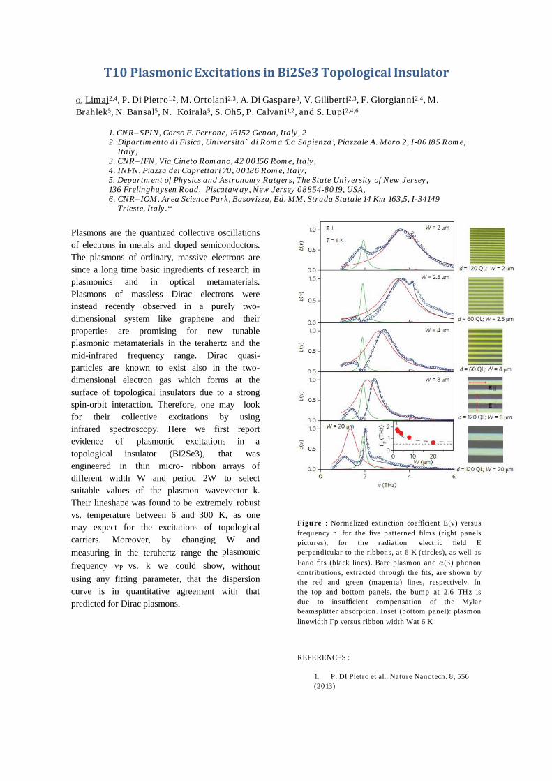
T10 Plasmonic Excitations in Bi2Se3 Topological Insulator
Plasmons are the quantized collective oscillations of electrons in metals and doped semiconductors. The plasmons of ordinary, massive electrons are since a long time basic ingredients of research in plasmonics and in optical metamaterials. Plasmons of massless Dirac electrons were instead recently observed in a purely two- dimensional system like graphene and their properties are promising for new tunable plasmonic metamaterials in the terahertz and the mid-infrared frequency range. Dirac quasi- particles are known to exist also in the two- dimensional electron gas which forms at the surface of topological insulators due to a strong spin-orbit interaction. Therefore, one may look for their collective excitations by using infrared spectroscopy. Here we first report evidence of plasmonic excitations in a topological insulator (Bi2Se3), that was engineered in thin micro- ribbon arrays of different width W and period 2W to select suitable values of the plasmon wavevector k. Their lineshape was found to be extremely robust vs. temperature between 6 and 300 K, as one may expect for the excitations of topological carriers. Moreover, by changing W and measuring in the terahertz range the plasmonic frequency νP vs. k we could show, without using any fitting parameter, that the dispersion curve is in quantitative agreement with that predicted for Dirac plasmons.
Figure : Normalized extinction coefficient E(ν) versus frequency n for the five patterned films (right panels pictures), for the radiation electric field E perpendicular to the ribbons, at 6 K (circles), as well as Fano fits (black lines). Bare plasmon and α(β) phonon contributions, extracted through the fits, are shown by the red and green (magenta) lines, respectively. In the top and bottom panels, the bump at 2.6 THz is due to insufficient compensation of the Mylar beamsplitter absorption. Inset (bottom panel): plasmon linewidth Γp versus ribbon width Wat 6 K
REFERENCES :
1. P. DI Pietro et al., Nature Nanotech. 8, 556 (2013)
O. Limaj2,4, P. Di Pietro1,2, M. Ortolani2,3, A. Di Gaspare3, V. Giliberti2,3, F. Giorgianni2,4, M. Brahlek5, N. Bansal5, N. Koirala5, S. Oh5, P. Calvani1,2, and S. Lupi2,4,6
1. CNR–SPIN, Corso F. Perrone, 16152 Genoa, Italy, 2 2. Dipartimento di Fisica, Universita` di Roma ‘La Sapienza’, Piazzale A. Moro 2, I-00185 Rome,
Italy, 3. CNR–IFN, Via Cineto Romano, 42 00156 Rome, Italy, 4. INFN, Piazza dei Caprettari 70, 00186 Rome, Italy, 5. Department of Physics and Astronomy Rutgers, The State University of New Jersey, 136 Frelinghuysen Road, Piscataway, New Jersey 08854-8019, USA, 6. CNR–IOM, Area Science Park, Basovizza, Ed. MM, Strada Statale 14 Km 163,5, I-34149
Trieste, Italy.*

T11 Photonic crystals: key nanostructures for light trapping and advanced solar cells C. Seassal1, L. Lalouat1,2, T. Deschamps1,2, R. Peretti1,2, H. Ding1,2, G. Gomard1,2, X.Q. Meng1,2, E. Drouard1, A. Fave2, F. Mandorlo2, R. Orobtchouk2, E. Fourmond2 Université de Lyon, Institut des Nanotechnologies de Lyon-INL, CNRS-ECL-INSA-UCBL-CPE Lyon 1Ecole Centrale de Lyon, 36 avenue Guy de Collongue, 69134 Ecully cedex, France 2 INSA de Lyon, Bat. Blaise Pascal, 7 avenue Jean Capelle, 69621, Villeurbanne, France The recent development of nanophotonics has triggered the emergence of novel concepts for light management in photovoltaic solar cells. This includes incident light trapping and strategies to control light absorption in thin film solar cells. Such novel approaches are based on various promising Nanophotonic structures, including planar photonic crystals, and their abilities to control light propagation and photon capture. The use of such nanophotonic concepts is expected to greatly increase the efficiency of moderate cost thin film solar cells. When combined with up- or down-conversion processes, these concepts could also be at the basis of ultra-high efficiency 3rd generation solar cells. This communication will include an overview of these Nanophotonic concepts. They will be illustrated by examples, with a particular focus on the emergence of photonic crystals-assisted thin film silicon solar cells (see Fig. 1). In particular, will discuss on the positive impact of such photonic nanostructures on the absorption, conversion efficiency and angular acceptance of solar cells (see Fig. 2).
Fig. 1: Schematic view and SEM view of a photonic crystal patterned thin film silicon solar cell
Fig. 2: Angular acceptance of a photonic crystal patterned thin silicon film solar cell

T12 Plasmons in low dimensional structures
F. Javier García de Abajo
ICFO - ICFO-The Institute of Photonic Sciences, Mediterranean Technology Park, Av. Carl Friedrich Gauss 3, 08860 Castelldefels (Barcelona), Spain
We will discuss recent advances in the study of plasmons in graphene and other low-dimensional structures, including thin films, and small organic molecules. In particular, we show that plasmons in graphene can be used to achieve electrical modulation of light in a robust, solid-state environment. Plasmons in polycyclic aromatic hydrocarbons, which can be regarded as small versions of graphene, are also shown to exhibit remarkable tunability and strong plasmonic response, thus revealing their potential for the new field of molecular plasmonics. Quantum effects in these systems, ranging from nonlocality to the discreteness of the electronic transitions involved, are shown to lead to exciting new physics and a wealth of potential applications, including a new paradigm for the design of molecular metamaterials.
Graphene has been shown to be capable of sustaining plasmons at mid-infrared frequencies when it is electrically
charged, for example via electrostatic gating [1-3]. This provides a robust tool for modulating the frequency of plasmons and the optical response of suitably structured materials. The modulation can be realized at ultrafast speeds in a compact, integrable, solid-state environment. The range of tunability covers a wide spectral range in the infrared, down to a measured wavelength of 3.7 microns [3]. Efforts to extend this range further towards the visible are underway, for example via intense doping of graphene. Graphene-related materials are also being considered.
In this work, we examine the recent progress made in graphene plasmonics and we explore potential applications to new classes of metamaterials. In particular, we discuss tunable complete optical absorption [4], ultrastrong coupling of optical emitters and graphene metasurfaces [5], and a new approach towards tunable, visible-range metamaterials based upon the use of molecular building blocks [6].
[1] J. Chen et al., “Optical nano-imaging of gate-tunable graphene plasmons”, Nature, vol. 487, 77-81 (2012). [2] Z. Fei et al., “Gate-tuning of graphene plasmons revealed by infrared nano-imaging”, Nature, vol. 487, 82-85 (2012). [3] Z. Fang et al., “Gated tunability and hybridization of localized plasmons in nanostructured graphene”, ACS Nano, vol.
7, 2388-2395 (2013). [4] S. Thongrattanasiri, F. H. L. Koppens and F. J. García de Abajo, “Complete optical absorption in periodically patterned graphene”,
Phys. Rev. Lett., vol. 108, 047401 (2012). [5] I. Silveiro, A. Manjavacas, S. Thongrattanasiri and F. J. García de Abajo, “”, New J. Phys., vol. 15, 033042 (2013).
[6] A. Manjavacas, F. Marchesin, S. Thongrattanasiri, P. Koval, P. Nordlander, D. Sánchez-Portal and F. J. García de Abajo, “Tunable molecular plasmons in polycyclic aromatic hydrocarbons”, ACS Nano, DOI: 10.1021/nn4006297.

T13 Control of metallic nanostructures within a silica layer by atomic force microscopy
S. Bakhti, C. Hubert, S. Reynaud, F. Vocanson and N. Destouches LHC, St. Etienne,FRANCE Optical properties of noble metal nanoparticles (NPs), characterized by localized surface plasmon resonances occuring in the visible spectrum, make them used in a wide range of applications. In most of them, a precise control of the NP size, shape and arrangement is of a great importance for tuning their optical properties. Among the different nanolithography techniques used to control these parameters, scanning probe microscopy based methods are well suited to inscribe metal structures with a nanometer precision. The approach used in this work consists in an electrochemically driven process of NPs formation [1]. A metal salt, contained in a thin film, is reduced locally under an Atomic Force Microscope (AFM) conductive tip by applying a voltage between the tip and a conductive substrate. Depending on the bias, nano-sized metal patterns can be grown within the film or on its top surface. In this work, silver nanostructures are grown and transformed in a silver salt impregnated mesoporous silica thin film deposited on an indium tin oxide (ITO) layer. A negative voltage applied to the AFM tip leads to the formation of silver structures on the silica surface, whose shape passes from nearly spherical to dendritic when the size increases. A positive voltage leads to the growth of silver islets embedded at the silica-ITO interface (Figure 1). We demonstrate the possibility to reversibly switch the nanostructure location between the top surface and the film-substrate interface by successively reversing the voltage polarity applied to the AFM tip. We also show that conductive channels can grow through the silica layer provided that large enough silver dendrites are grown on the silica surface. Such channels are cut when switching the tip bias. The electrical properties of the silica layer can then be locally modified and the film is reversibly switched from conductive to insulator by applying respectively negative and positive voltages to the tip.
Figure 1. (a) Negative and (b) positive voltage applied to the tip lead respectively to the formation of silver nanostructures on the silica surface and at the silica-ITO interface position [1] C. Hubert, H. Amrani, M. Ali Khan, F. Vocanson, N. Destouches, Appl. Phys. Lett. 2012, 100, 241605.
T14 Effective Medium Approach to Response of Adsorption-Based Nanoplasmonic Chemical Sensors
Zoran Jakšić, Olga Jakšić, Ivana Jokić, Slobodan Vuković, Dana Vasiljević-Radović Center of Microelectronic Technologies, Institute of Chemistry, Technology and Metallurgy, University of Belgrade, Njegoševa
12, 11000 Belgrade, Serbia [email protected]
Among the important applications of plasmonic nanostructures are affinity-based sensors [1, 2]. The effects of adsorption and desorption can be utilized in both nanoparticle-based systems with localized surface plasmon resonance (SPR) and in ordered subwavelength plasmonic crystals/plasmonic metamaterials, where the possibility to tailor frequency response ensures a new degree of freedom in sensor design [3, 4].
Contrary to conventional SPR sensors, where electromagnetic (EM) field is constant along the surface and evanescently varies only in the direction perpendicular to it, the field distribution in a nanoplasmonic sensor is determined by the geometry of its unit cell, assumes a more complex form (to the point that high-intensity hotspots may appear) and generally may vary along any of the three Cartesian axes. In addition to it, the unit cell itself is composed from at least two different materials (with positive and with negative permittivity parts) thus resulting in a surface heterogeneity and a spatial variation of the adsorption properties [5]. This means that in a given spot at the sensor surface the response to a specific adsorbate will vary in dependence on both the local adsorption energy and on the local field intensity.
We propose to introduce a synthetic parameter that describes the effective adsorption from the point of view of electromagnetic behavior of the sensor taking into account the spatial distribution of the adsorption properties and the electromagnetic fields across the sensor. It assumes the form of a multiplicative coefficient that relates the response of a real heterogeneous structure (both in adsorption and in electromagnetic sense) to an effective homogeneous (averaged) structure.
In a general case this parameter can be calculated by integrating across the unit cell the mean value of the product of the local surface density of adsorbate and the corresponding EM field. We further consider an approach to determine an approximation to this effective adsorption coefficient by using the effective medium approximation and assuming that the field maxima are located in the vicinity of metal/plasmonic material parts. One of the possible approaches then is to use the simple Maxwell-Garnett formula utilizing the metal filling factor to assess the overall influence of the adsorbate. The further calculation is reduced to the determination of the number of the adsorbed particles. One is thus able to utilize the complete existing mathematical apparatus of stochastic analysis [6] to calculate the adsorption and determine the response and noise level of the nanoplasmonic/metamaterial sensor.
[1] Choi, I. and Choi, Y., 2012 Plasmonic nanosensors: Review and prospect IEEE J. Sel. Top. Quant. Electr. 18 1110. [2] Anker, J. N.; Hall, W. P.; Lyandres, O.; Shah, N. C.; Zhao, J. and Van Duyne, R. P., 2008 Biosensing with plasmonic
nanosensors Nat. Mater. 7 442. [3] Jakšić, Z.; Jakšić, O.; Djurić, Z. and Kment, C., 2007 A consideration of the use of metamaterials for sensing
applications: Field fluctuations and ultimate performance J. Opt. A-Pure Appl. Opt. 9 S377. [4] Jakšić, Z., 2010 Optical metamaterials as the platform for a novel generation of ultrasensitive chemical or biological
sensors. Metamaterials: Classes, Properties and Applications; ed Tremblay, E. J.; (Hauppauge, New York: Nova Science Publishers); p. 1.
[5] Rudzinski, W., Everett, D.H., 1991 Adsorption of Gases on Heterogeneous Surface, Academic Press, New York [6] Jakšić, O. M.; Jakšić, Z. S.; Čupić, Ž. D.; Randjelović, D. V. and Kolar-Anić, L. Z., 2014 Fluctuations in transient
response of adsorption-based plasmonic sensors Sensors and Actuators B: Chemical 190 419.

T15 A New Way to Tame Light: Electrically controlled resistive switching assisted active broadband optical
tunability
Ali Kemal Okyay Bilkent University, Ankara, TURKEY
Active control of the optical properties of materials have always been of significance due to its various applications such as tunable optical filters, beam steering, adaptive sensors and holographic devices. Recently, nonlinear, electro-optic, magneto-optic, phase change materials, doped semiconductors, liquid crystals, micromechanical structures have been realized in order to gain control over the refractive index of an optical media. Yet, achieving optical tunability in a broad spectrum remains a challenge.
In this talk I will discuss an electrically tunable optical device exhibiting ultra-broadband tunability characteristic in the mid-infrared spectrum. The proposed device consists of a p-n junction formed by ZnO/p-Si and an inherent resistive switch realized by addition of a metallic top contact (Al/ZnO/p-Si). This is the first observation of hysteresis in the reflection spectra due to resistive switching.
T16 Recent Improvements in Plasmonic Biosensing Techniques I. Abdulhalim
Department of Electrooptic Engineering and The Ilse Katz Institute for Nanoscale Sciences and Technology, Ben Gurion
Unevirsity, Beer Sheva 84105, Israel
Plasmonic sensors include surface plasmon resonance (SPR) related phenomena on metallic surfaces. SPR sensors based on extended SP waves are a mature technology for more than two decades now, however recent investigations show continuous enhancement of their sensitivity and their lower detection limit. Together with the recent investigations in localized SPR (LSPR) phenomena, extraordinary optical transmission through nanoapertures in metals, and surface enhanced spectroscopies, drastic developments are expected to revolutionize the field of optical sensing. It is shown that in the majority of cases the sensitivity enhancement is associated with the enhancement of the electromagnetic field (EM) overlap integral describing the electromagnetic interaction energy within the analyte. This means the enhancement is achieved by enhancing the EM field at the metal-analyte interface, increasing the interaction volume for example by increasing the penetration depth or by using porous materials. The detection limit on the other hand is determined by the sensitivity and the precision of the system, hence in addition to sensitivity improvement one has to take care also of the improvement in the system precision. Examples will be presented starting from the well-known Kretschmann configuration through the addition of high index dielectric thin film to the metal, the addition of gratings, the use of nanoSculptured thin films (nanoSTFs) and enhanced transmission of nanoslits. Special attention will be given to nanoSTFs which are assemblies of shaped, parallel and tilted nanorods, prepared using many variants of the basic Glancing Angle Deposition (GLAD) technique. Because of the special shapes and nanoscale dimensions of STFs, they exhibit a great potential in the SPR biosensing field. For the improvement of the detection limit a divergent beam imaging approach was developed which improves the precision of the angular interrogation technique by more than an order of magnitude. Combination of the addition of nanolayer and longer wavelength is shown to improve the figure of merit and allow detection of bacteria cells in water. References:
1. A. Shalabney and I. Abdulhalim, Electromagnetic fields distribution in multilayer thin film structures and the origin of sensitivity enhancement in surface plasmon resonance sensors, Sensors and Actuators A, 159, 24-32 (2010).
2. Amit Lahav, Mark Auslender and I. Abdulhalim, Sensitivity enhancement of guided wave surface plasmon resonance sensors, Opt.Lett. 33, 2539-2541 (2008).
3. I. Abdulhalim, Alina Karabchevsky et.al., Surface enhanced fluorescence from metal sculptured thin films with application to biosensing in water, App.Phys.Lett. 94, 063206 (2009).
4. Alina Karabchevsky et.al., Theoretical and experimental investigation of enhanced transmission through periodic metal nanoslits for sensing in water environment, Journal of Plasmonics, 4, 281-292 (2009).
5. Atef Shalabney and I. Abdulhalim, Sensitivity enhancement methods for surface plasmon sensors, Lasers and Photonics Reviews, 5, 571-606 (2011). DOI 10.1002/lpor.201000009.
6. A. Karabchevsky et.al., Nano-precision algorithm for surface plasmon resonance determination from images with low contrast for improved sensor resolution, J. NanoPhotonics, 5, 051813-12 (2011). DOI: 10.1117/1.3598138.
7. Atef Shalabney et.al., Sensitivity of surface plasmon resonance sensors based on metallic columnar thin films in the spectral and angular interrogations, Sensors and Actuators B: Chemical, 159, 201-212 (2011).
8. Olga Krasnykov et.al., Sensor with increased sensitivity based on enhanced optical transmission in the infrared, Opt.Commu., 284, 1435-1438 (2011).
9. Atef Shalabney and I. Abdulhalim, Figure of merit enhancement of surface plasmon resonance sensors in the spectral interrogation, Optics Letters 37, 1175 (2012).
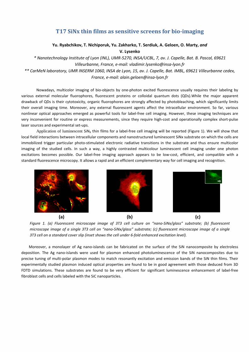
T17 SiNx thin films as sensitive screens for bio-imaging
Yu. Ryabchikov, T. Nichiporuk, Yu. Zakharko, T. Serdiuk, A. Geloen, O. Marty, and V. Lysenko
* Nanotechnology Institute of Lyon (INL), UMR-5270, INSA/UCBL, 7, av. J. Capelle, Bat. B. Pascal, 69621 Villeurbanne, France, e-mail: [email protected]
** CarMeN laboratory, UMR INSERM 1060, INSA de Lyon, 15, av. J. Capelle, Bat. IMBL, 69621 Villeurbanne cedex, France, e-mail: [email protected]
Nowadays, multicolor imaging of bio-objects by one-photon excited fluorescence usually requires their labeling by
various external molecular fluorophores, fluorescent proteins or colloidal quantum dots (QDs).While the major apparent drawback of QDs is their cytotoxicity, organic fluorophores are strongly affected by photobleaching, which significantly limits their overall imaging time. Moreover, any external fluorescent agents affect the intracellular environment. So far, various nonlinear optical approaches emerged as powerful tools for label-free cell imaging. However, these imaging techniques are very inconvenient for routine or express measurements, since they require high-cost and operationally complex short-pulse laser sources and experimental set-ups.
Application of luminescent SiNX thin films for a label-free cell imaging will be reported (Figure 1). We will show that local field interactions between intracellular components and nanostructured luminescent SiNx substrate on which the cells are immobilized trigger particular photo-stimulated electronic radiative transitions in the substrate and thus ensure multicolor imaging of the studied cells. In such a way, a highly contrasted multicolour luminescent cell imaging under one photon excitations becomes possible. Our label-free imaging approach appears to be low-cost, efficient, and compatible with a standard fluorescence microcopy. It allows a rapid and an efficient complementary way for cell imaging and recognition.
(a) (b) (c)
Figure 1. (a) Fluorescent microscope image of 3T3 cell culture on “nano-SiNx/glass” substrate; (b) fluorescent microscope image of a single 3T3 cell on “nano-SiNx/glass” substrate; (c) fluorescent microscope image of a single 3T3 cell on a standard cover slip (inset shows the cell under 6-fold enhanced excitation level). Moreover, a monolayer of Ag nano-islands can be fabricated on the surface of the SiN nanocomposite by electroless
deposition. The Ag nano-islands were used for plasmon enhanced photoluminescence of the SiN nanocomposites due to precise tuning of multi-polar plasmon modes to match resonantly excitation and emission bands of the SiN thin films. Their experimentally studied plasmon induced optical properties are found to be in good agreement with those deduced from 3D FDTD simulations. These substrates are found to be very efficient for significant luminescence enhancement of label-free fibroblast cells and cells labeled with the SiC nanoparticles.
×6
T18 Real-time sensing of enteropathogenic E. coli induced effects on epithelial host cell height and cell-substrate interactions by infrared surface plasmon
spectroscopy
Victor Yashunsky1,3*$, Leorah Kharilker2$, Efrat Zlotkin-Rivkin2, David Rund2, Naomi Melamed-Book6, Eitan
Zahavi4, Eran Perlson4, Silvana Mercone5, Michael Golosovsky1, Dan Davidov1, Benjamin Aroeti2
1 The Racah Institute of Physics, the Hebrew University of Jerusalem, 91904 Jerusalem, Israel 2 Department of Cell and Developmental Biology, and the Bioimaging Unit6 The Alexander Silberman Institute of Life
Sciences,The Hebrew University of Jerusalem, 91904 Jerusalem, Israel 3The Institute of Biochemistry, Food Science and Nutrition Robert H. Smith Faculty of Agriculture, Food and Environment, The
Hebrew University of Jerusalem, Rehovot 76100, Israel 4Department of Physiology and Pharmacology, Sackler Faculty of Medicine, Tel-Aviv University, Ramat Aviv, Tel Aviv 69978,
Israel 5Université Paris 13, Sorbonne Paris Cité, LSPM–(UPR 3407) CNRS, 99 Avenue J.-B. Clément, 93430 Villetaneuse.
Enteropathogenic Escherichia coli (EPEC) is an important, generally non-invasive, bacterial pathogen that
causes diarrhea in humans. The microbe infects mainly the enterocytes of the small intestine. Here we have
applied our newly developed infrared surface plasmon resonance (IR-SPR) spectroscopy approach to study
the effects of EPEC infection on epithelial host cells. The IR-SPR experiments showed that EPEC infection
results in a robust reduction in the refractive index of the infected cells. Assisted by confocal and total
internal reflection microscopy we discovered that the microbe dilates the intercellular gaps and induces the
appearance of fluid-phase filled pinocytic vesicles in the lower basolateral regions of the host epithelial
cells. Partial cell detachment from the underlying substratum was also observed. Finally, our IR-SPR
analyses showed that EPEC infection somewhat decreases the host cell height. Together, these observations
reveal novel impacts of the pathogen on the host cell architecture and endocytic functions. We suggest that
these changes associated with the infiltration of a watery environment into the host cell, disrupting the host
cell monolayer architecture and integrity. All these can potentially lead to failure of the epithelium barrier
functions and to the diarrheal effect. Our findings also demonstrate the great potential of the label-free IR-
SPR approach to study the dynamics of host-pathogen interactions with high spatiotemporal sensitivity.

T19 Optofluidic chip with integrated photonic tweezers
C. Pin1,2,3, C. Renaut1,2,3, E. Picard2, E. Hadji2, D. Peyrade3, F. de Fornel1, B. Cluzel1 1 : Groupe d’Optique de Champ Proche – LRC CEA n°DSM-08-36, Laboratoire ICB. UMR
CNRS 6303 - Université de Bourgogne, France 2 : SiNaPS lab./SP2M, UMR-E CEA/UJF-Grenoble1, INAC, Grenoble, F38054, France
3 : CNRS/UJF-Grenoble/CEA LTM, 17 rue des Martyrs, 38054 Grenoble cedex9, France [email protected]
In order to design future lab-on-a-chip, integrated tools for trapping and manipulation of micro- and nano-objects are needed. In this work, optofluidic chips with integrated photonic tweezers are fabricated by adding a polydimethylsiloxane (PDMS) microfluidic chanel on top of silicon-on-insulator (SOI) photonic “nanobeam” cavities [1]. The light resonance inside such a photonic cavity leads to a high spectral and spatial confinement of the elecromagnetic field. This light confinement generates strong and localized gradient forces in the near field of the cavity. These optical forces are used to trap, detect, assemble and manipulate micro- and nanoparticles [2-5]. The microfluidic circuit allows controlled injection of small volumes of colloidal solution.
The trap stiffness of the presented on-chip optical tweezers is deduced from the trajectory of trapped polystyrene microparticles. A lateral stiffness of 5 pN.µm-1 is measured, whereas it is found to decrease to 0.6 pN.µm-1 along the waveguide axis. In addition, trapped particles of 1µm in diameter have been proved to resist to a lateral force of circa 10 -1pN generated by a weak flow pulse. The particle displacement is consistent with the above measured trap stiffness.
Finally, designing photonic nanocavities directly within the optical waveguide enables to precisely record the influence of a trapped particle on the cavity resonance. The transmitted signal shows for instance a different correlation time depending on the particle motion. This property is used to distinguish particles of 1µm and 2µm diameter. Therefore, the analysis of the signal transmitted by photonic tweezers is believed to be a valuable way towards future lab-on-a-chip.
10 µm
flow trapped particle
Figure 1. Microscopic observation of a particle (1µm diameter) trapped on a “nanobeam” cavity in a flow of colloidal
solution References: [1] Vehla, P. et al., “Ultra-high Q/V Fabry-Perot microcavity on SOI substrate”, Optics Express, vol.15, no.24, pp.16090-16096, 2007 [2] Serey, X., Mandal, S. and Erickson, D., “Comparison of silicon photonic crystal resonator designs for optical trapping of
nanomaterials”, Nanotechnology, vol.21, no.30, 305202, 2010 [3] Lin, S., Zhu, W., Jin, Y. and Crozier, K. B., “Surface-Enhanced Raman Scattering with Ag Nanoparticles Optically Trapped by a Photonic
Crystal Cavity”, Nanoletters, vol.13, no.2, pp.559-563, 2013 [4] Renaut, C. et al., “Assembly of microparticles by optical trapping with a photonic crystal nanocavity”, Applied Physics Letters, vol.100,
no.10, 101103, 2012 [5] Renaut, C. et al., “On chip shapeable optical tweezers”, Scientific Reports, vol.3, 2290, 2013
T20 Nanophotonic periodic structures with reduced symmetry Hamza Kurt TOBB University, Ankara, TURKEY
While high symmetry in periodic nano-photonic structures is desirable in some applications intentionally introducing low symmetry to the unit cell of the same type of structures yields spectrally rich equi-frequency contours. Due to the intrinsic dispersive feature of the designed artificial medium, the incident signal with different wavelengths can be successfully separated in the spatial domain without incorporating any type of defects. In addition to efficient wavelength selectivity, super-collimation of light over a broad bandwidth can also be succeeded by taking the advantage of the reduced symmetry. The talk will present an overview of the possible applications of periodic structures with reduced symmetry.
T21 Linear and nonlinear Optical responses of a single Bi-metallic nanoparticle
Anna Lombardi, Etienne Pertreux, Aurélien Crut, Paolo Maioli, Natalia Del Fatti, and Fabrice Vallée
FemtoNanoOptics Group, ILM, Universite Lyon 1 – CNRS,
Bâtiment Kastler, 43 Bd du 11 Novembre, 69622 Villeurbanne - France email: [email protected]
The size, shape and structure dependencies of the physical and chemical properties of nano-objects, and the concomitant possibilities opened for their control and tailoring to specific applications, have led to considerable activities in the academic and industrial domains. In particular, the impacts of size reduction on the optical properties of nano-objects formed by a single material, e.g., a metal or a semiconductor, have been extensively experimentally and theoretically investigated, and are now well understood. Nano-hybrids, i.e., nano-objects formed by different materials (e.g., organic-inorganic or inorganic-inorganic as metal–semiconductor or metal–dielectrics) offer even more possibilities by combining of the nanoscale responses of their components, but also raises fundamental questions on the interactions of the constituting materials. However, they have been much less studied because of the difficulty of their synthesis and of their optical investigation that has to be performed at the single object level to avoid spurious effect due to dispersion of their morphology.
After introducing our experimental method for investigating the linear and nonlinear optical response of a
single nano-object, namely spatial modulation spectroscopy (SMS), we will discuss the optical response of a model metal nano-hybrid: a hetero-dimer formed by a gold nanoparticle in contact with a silver nanoparticle coated by a silica shell (Au-Ag@SiO2 dimers). Optical measurements were performed on single dimers whose individual morphologies are determined using transmission electron microscopy (TEM) [1,2], permitting quantitative comparison between the measured spectra and the results of numerical simulations. In particular interaction of the gold and silver particles in a dimer is theoretically shown to modulate the gold absorption spectra, an effect that can be experimentally evidenced using time-resolved nonlinear spectroscopy.
[1] O. Muskens et al., Phys. Rev. B 78, 205410 (2008). [2] A. Lombardi et al., ACS Nano, 7, 2522 (2013).

T22 Locally Resonant Metamaterials: Focusing, Imaging and Manipulating Waves at the Deep Subwavelength Scale
Geoffroy Lerosey Institut Langevin, ESPCI ParisTech & CNRS, Paris, France
In this talk I will present some of our recent works on metamaterials based on resonant unit cells. I will show how the use of time dependent and broadband wavefields, in conjunction with those metamaterials,
permits to beat the diffraction limit from the far field for imaging or focusing purposes. I will introduce the idea of resonant metalens, first demonstrated in the microwave domain, and explain its principles. In particular, I will show how the concept of time reversal can be utilized to focus in this metamaterial based lens and from the far field, onto focal spots much smaller than the diffraction limit [1]. I will then prove the generality of the approach by demonstrating its transposition to the acoustic domain [2] thanks to a very simple setup: an array of soda cans (Figure a). Then I will present our latest theoretical and numerical results obtained using a resonant metalens made out of plasmonic nanorods in the visible part of the spectrum [3].
Finally I will then prove that since some of those media are solely governed by interference effects, it is possible to go beyond the effective medium theory usually used in this field, and adopt a microscopic approach to these metamaterials. In particular I will show that those media can be modified locally at will in order to confine, guide, bend, or split waves (Figure b), just like it is realized in photonic or phononic crystals, yet on dimensions that are much smaller, i.e. that are deeply subwavelength. This approach, which fills the gap between photonic crystals and metamaterials, will be experimentally demonstrated with acoustic and electromagnetic waves [4,5].
Figure 1: a) deep subwavelength focal spot obtained using far field time reversal on top of an array of soda cans, and b) waveguiding
microwaves at the deep subwavelength scale in an array of locally modified resonant electric wires
1 - Lemoult, F., Lerosey, G., de Rosny, J. and Fink, M. “Resonant Metalenses for Breaking the Diffraction Barrier”. Physical Review Letters 104, 203901, (2010). 2 - Lemoult, F., Fink, M. and Lerosey, G. “Acoustic resonators for far field control of sound on a subwavelength scale”. Physical Review Letters 107, 064301 (2011). 3 - Lemoult, F., Fink, M. and Lerosey, G. “A polychromatic approach to far field superlensing at visible wavelengths”. Nature Communications 3, 889 (2012). 4 - Lemoult, F., Kaïna, N., Fink, M. and Lerosey, G. “Wave propagation control at the deep subwavelength scale in metamaterials”. Nature Physics 9, 55–60 (2013). 5 - Kaïna, N., Lemoult, F., Fink, M. and Lerosey, G. “Ultra-low mode volumes defect cavities in ordered and disordered metamaterials”. Applied Physics Letters 102, 144104 (2013).
T23 Taming blackbody radiation with surface waves: near field
Jean-Jacques Greffet 1, A Babuty2, Y de Wilde2, K. Joulain3, O. Chapuis4, R. Messina5, P. Ben-Abdallah1
1Laboratoire Charles Fabry, Institut d'Optique, CNRS, Palaiseau, France 2Institut Langevin, ESPCI, CNRS, Paris, France
3Institut P', CNRS, Poitiers, France 4Cethil, INSA, CNRS, Lyon, France
5Laboratoire Charles Coulomb, Université Montpellier 2, CNRS, Montpellier, France It has been predicted ten years ago that thermal emission by a surface can be quasimonochromatic and enhanced by orders of magnitude close to a surface. These effects are due to the thermal excitation of surface phonon polaritons. Although the observation of enhanced thermal fields close to a surface was reported in 2006, the observation of the predicted narrow spectrum has only be reported recently [1,2]. In this talk, we will report measurements performed at ESPCI in the group of Yannick de Wilde. We will also discuss how the deposition of a graphene layer modifies the near-field thermal radiation on a SiC surface. This effect paves the way to the electrical control of the local density of states in the near field. [1] A Babuty et al. Phys.Rev.Lett. 110, 146103 (2013) [2] R. Messina et al. , Phys.Rev.B 87, 085421 (2013)

T24 Time-Resolved and Ultra-Sensitive Vibrational Biospectroscopy with Mid-Infrared Plasmonics
Hatice Altug, Ronen Adato, Serap Aksu, Dordaneh Etezadi
Boston Univ. and EPFL in Switzerland
abstract: We will present a nanoplasmonic chip based technology for performing ultra-sensitive infrared absorption spectroscopy in aqueous solutions, capable of monitoring biomolecule interactions at the sub-monolayer level in real-time. These measurements are made possible by plasmonic enhancements of absorption bands in conjunction with a non-classical form of internal reflection that dramatically boost sensitivity and surface selectivity to limit strong interference from water. Our on-chip technology integrated with microfluidics represents a dramatic advancement in the compatibility of IR absorption spectroscopy with modern and next generation sample preparation and handling techniques.

T25 Terahertz and Infrared Plasmonics and Metasurfaces Tahsin Akalin
IEMN, UMR CNRS 8520, Lille 1 University, France
In the terahertz and infrared frequency range, simulation and experimental results on transmission lines and on flat antennas and lenses obtained with original approaches will be presented and discussed. In the first part, the studied transmission lines present the particularity to be made with a single conductor in planar technology. These lines are called Planar Goubau Lines (PGL). The efficient excitation [1] of the highly confined propagating radial mode on a metallic strip will be described and we will present the optimization of transmission properties in the THz range. Based on this preliminary study, an overview will be given on fundamental plasmonic and metamaterials inspired topologies such as band reject and bandpass filters [2], by using two different approaches. In the first approach, the corrugations of the PGL are designed in order to reject frequency bands when the period is comparable to the half of the guided wavelength or to obtain a slow wave effect when the corrugations have a subwavelength distribution. Resonators like split ring resonators (SRR) are used in the second approach to obtain different behaviors when they are coupled with the PGL. We will compare the response of metasurfaces made of SRR arrays to the case when only few number resonators (as represented on Fig. 1) are coupled to the PGL [3]. Bendings and broadband power splitters can also be obtained with the use of this PGL. Based on these interesting properties we have also designed structures for on chip THz microscopy.
In a second part, we will present flat structures with useful properties at terahertz and infrared frequencies. The first structures are bull's-eye antennas as proposed by Prof. Ebbesen [4] and the second ones are flat lenses as proposed by Prof. Capasso. We will describe the fabrication techniques of the antennas and their radiation properties [5]. The antennas are made with one dimensional or two dimensional periodic corrugations with different shapes: triangular (Fig. 1), rectangular and sinusoidal lateral shapes. The flat lenses are based on arrays with V-shaped antennas and we will present their focusing properties. The perspectives on each topic will end the talk. References: [1] T. Akalin et al, “Single-wire transmission lines at terahertz frequencies,” IEEE Transactions on Microwave Theory and Techniques, vol. 54, no. 6, pp. 2762–2767, 2006. [2] Ali K. Horestani, Withawat Withayachumnankul, Abdallah Chahadih, Abbas Ghaddar, Mokhtar Zehar, Derek Abbott, Christophe Fumeaux, and Tahsin Akalin, "Metamaterial-Inspired Bandpass Filters for Terahertz Surface Waves on Goubau Lines" to be published in IEEE-Terahertz Science and Technology 2013 [3] W.-C. Chen, J. J. Mock, D. R. Smith, T. Akalin, and W. J. Padilla, “Controlling gigahertz and terahertz surface electromagnetic waves with metamaterial resonators,” Physical Review X, vol. 1, no. 2, p. 021016, Dec. 2011. [4] T. W. Ebbesen, H. J. Lezec, H. F. Ghaemi, T. Thio, and P. A. Wolff, “Extraordinary optical transmission through sub-wavelength hole arrays,” Nature, vol. 391, pp. 667–669, Feb. 1998. [5 ] Miguel Beruete, Unai Beaskoetxea, Mokhtar Zehar, Amit Agrawal, Shuchang Liu, Karine Blary, Abdallah Chahadih, Xiang-Lei Han, Miguel Navarro-Cía, David Etayo, Ajay Nahata, Tahsin Akalin and Mario Sorolla Ayza, "Terahertz Corrugated and Bull's eye antennas" to be published in IEEE-Terahertz Science and Technology 2013
Fig.1 On the left, Planar Goubau Lines with (structure F) and without coupled SRR (reference).
On the right, corrugated antenna with triangular corrugations for THz frequencies

T26 Instabilities and Rogue Waves in Nonlinear Fiber Optics
P.A. Lacourt, F. Dias, G. Genty and J. M. Dudley FEMTO ST,Besançon, France Abstract: Recent work in nonlinear fiber optics has demonstrated qualitative and quantitative links between instabilities in optical propagation and the giant destructive rogue or freak waves on the surface of the ocean. The analogy between the appearance of instabilities in optics and the rogue waves on the ocean’s surface is both intriguing and attractive, as it opens up possibilities to explore the extreme value dynamics in a convenient benchtop optical environment. The purpose of this talk will be to discuss the results that have been obtained in optics, and to consider both the similarities and the differences with oceanic rogue wave counterparts. The talk will review experimental work in this field and will cover rogue waves in supercontinuum generation and the formation of localized new classes of soliton on finite background. New experimental techniques to directly reveal real-time noise and rogue wave signatures across the full bandwidth of an optical supercontinuum will also be described.
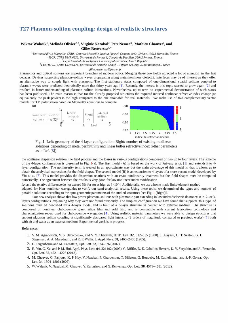
T27 Plasmon-soliton coupling: design of realistic structures
Wiktor Walasik1, Melinda Olivier2,3, Virginie Nazabal2, Petr Nemec3, Mathieu Chauvet4, and
Gilles Renversez1,∗ 1Universite d’Aix-Marseille, CNRS, Centrale Marseille, Institut Fresnel, Campus de St. Jerome, 13013 Marseille, France
2ISCR, CNRS UMR 6226, Universite de Rennes I, Campus de Beaulieu, 35042 Rennes, France 3Department of Photophysics, University of Pardubice, Czech Republic
4FEMTO-ST, CNRS UMR 6174, Universite de Franche-Comte, 16 Route de Gray, 25000 Besancon, France [email protected]
Plasmonics and optical solitons are important branches of modern optics. Merging those two fields attracted a lot of attention in the last decades. Devices supporting plasmon–soliton waves propagating along metal/nonlinear dielectric interfaces may be of interest as they offer an alternative way to couple light with plasmons. The first stationary states composed of one-dimensional spatial solitons coupled to plasmon waves were predicted theoretically more that thirty years ago [1]. Recently, the interest in this topic started to grow again [2] and resulted in better understanding of plasmon–soliton interactions. Nevertheless, up to now, no experimental demonstration of such states has been published. The main reason is that for the already proposed structures the required induced nonlinear refractive index change (or equivalently the peak power) is too high compared to the one attainable for real materials. We make use of two complementary vector models for TM polarisation based on Maxwell’s equations to compute
Fig. 1. Left: geometry of the 4-layer configuration. Right: number of existing nonlinear solutions depending on metal permittivity and linear buffer refractive index (other parameters as in Ref. [5])
the nonlinear dispersion relation, the field profiles and the losses in various configurations composed of two up to four layers. The scheme of the 4-layer configuration is presented in Fig. 1(a). The first model (A) is based on the work of Ariyasu et al. [1] and extends it to 4-layer configuration. The nonlinearity term is treated in an approximate way but the main advantage of this model is that it allows us to obtain the analytical expressions for the field shapes. The second model (B) is an extension to 4 layers of a more recent model developed by Yin et al. [3]. This model provides the dispersion relations with an exact nonlinearity treatment but the field shapes must be computed numerically. The agreement between the results is very good for low nonlinear index modification ∆n and the relative difference do not exceed 5% for ∆n as high as 3 · 10−2. Additionally, we use a home made finite-element method adapted for Kerr nonlinear waveguides to verify our semi-analytical results. Using these tools, we determined the types and number of possible solutions according to the opto-geometric parameters of the studied structures [see Fig. 1 (Right)].
Our new analysis shows that low power plasmon–solitons with plasmonic part extending in low index dielectric do not exist in 2- or 3-layers configurations, explaining why they were not found previously. The simplest configuration we have found that supports this type of solutions must be described by a 4-layer model and is built of a 3-layer structure in contact with external medium. The structure is composed of nonlinear chalcogenide glass, silica film and gold film, and is compatible with current fabrication technology and characterization set-up used for chalcogenide waveguides [4]. Using realistic material parameters we were able to design structures that support plasmon–soliton coupling at significantly decreased light intensity (2 orders of magnitude compared to previous works) [5] both with air and water as an external medium. Experimental work is in progress.
References
1. V. M. Agranovich, V. S. Babichenko, and V. Y. Chernyak, JETP. Lett. 32, 512–515 (1980). J. Ariyasu, C. T. Seaton, G. I. Stegeman, A. A. Maradudin, and R. F. Wallis, J. Appl. Phys. 58, 2460–2466 (1985).
2. E. Feigenbaum and M. Orenstein, Opt. Lett. 32, 674–676 (2007). 3. H. Yin, C. Xu, and P. M. Hui, Appl. Phys. Lett. 94, 221102 (2009). C. Milian, D. E. Ceballos-Herrera, D. V. Skryabin, and A. Ferrando,
Opt. Lett. 37, 4221–4223 (2012). 4. M. Chauvet, G. Fanjoux, K. P. Huy, V. Nazabal, F. Charpentier, T. Billeton, G. Boudebs, M. Cathelinaud, and S.-P. Gorza, Opt.
Lett. 34, 1804–1806 (2009). 5. W. Walasik, V. Nazabal, M. Chauvet, Y. Kartashov, and G. Renversez, Opt. Lett. 38, 4579–4581 (2012).
(a) -90 3
-100 2
-110
-120 1 1 1.25 1.5 1.75 2 2.25 2.5
indice de réfraction linéaire

T28 A feasibility study for controlling self-organized production of plasmonic enhancement interfaces for solar cells Alpan Bek, Mona Zolfaghariborra, Seda Kayra Güllü, Hisham Nasser Middle East Technical University Physics Department, AnKara, Turkey
Localized surface plasmon oscillations induced in metal particles by an electromagnetic field is expected to be useful in light trapping applications in solar cells. This is based on the prediction of an improvement in the energy conversion efficiency through either near field enhancement effect in the close vicinity of the particles, or through an improved effective scattering into the active area of the solar cell. In the last decade, many theoretical and design studies on different metal nanoparticle-solar cell systems have predicted significant increase in solar cell efficiency. These predictions are generally based on well-defined, regularly distributed nanoparticle systems with ideal optical properties. In reality, most of the experimental studies deal with randomly distributed nanoparticles that are prepared from thin metal films by thermally induced self-organized dewetting of the underlying substrate surface. Even in the case of size wise mono-disperse and periodic nanostructure systems fabricated by sophisticated techniques such as e-beam lithography, a small deviation from the intended structure shape or size causes significant changes in the resultant optical spectrum of the system. It was indeed shown that the shape, size, and distribution of metal nanoparticles should be carefully controlled in order to create a positive impact on solar cell performance. Any parasitic absorption by the nanoparticles might lead to a loss in the supply of the light into the active cell area. As a result, the experimental studies have not been able to undoubtedly demonstrate the expected breakthrough with respect to the state-of-the art solar cells with light trapping structure based on traditional surface texturing. Ag nanoparticles (AgNPs) are of particular interest in solar cell research for their preferable resonance behaviour in the visible spectrum. They can be prepared either by high resolution lithography or by techniques which are relatively more appropriate for mass production such as dewetting and self-assembly methods. Recently, several studies have reported on the different aspects of AgNP-solar cell systems that are fabricated by both techniques. However yet, the effect of the substrate on the formation kinetics of the nanoparticles and the optical properties of the combined system are not studied intensively. In this presentation, I report on dewetting based fabrication and optical responses of AgNPs on 5 different solar cell technology relevant material surfaces which are widely used, namely Si, SiO2, Si3N4, In:SnO (ITO), and Al:ZnO (AZO). These material systems are of interest as they are used in the front and back surfaces of c-Si and thin film solar cells or as intermediate layers for various functionalities. The results of such a comparative study on these various solar cell technology relevant substrate surfaces will be highly beneficial and may help paving the way to discovery of the most important factors for controlling the average nanoparticle size, and the breadth of the size distribution. Optical properties of a 2D array of AgNPs are known to be very sensitive to these properties. I will demonstrate that these properties strongly depend on the type of the substrate used. I will report on a correlation between average nanoparticle size and its distribution and substrate thermal conductivity and surface roughness.
T29 Enhancing light matter interactions using nanoscale integration of silicon, metal and vapors
Ilya Goykhman, Boris Desiatov, Liron Stern and Uriel Levy,
Department of Applied Physics, The school of computer science and engineering, The Center for Nanoscience and Nanotechnology, The Hebrew University of Jerusalem, Jerusalem, 91904, Israel
Abstract:
Motivated by the ongoing effort for miniaturization, on chip nanoscale photonic and plasmonic based devices and components are being explored and developed in variety of configurations and are being used for a variety of applications. Further progress in the development of nanoscale photonic and plasmonic components rely on proper choice of material platforms and the capabilities to fuse integrate these platforms together on a chip. In this talk we discuss some of our recent achievements in the field of nanoscale optoelectronic devices taking advantage of strong light matter interactions on a chip. Specifically, we exploit the silicon plasmonics and the silicon photonics platforms for the demonstration of light modulation and detection in the IR regime. Furthermore, we also demonstrate strong light vapor (Rubidium) interactions on a chip, with saturation of atomic transitions at power levels in the nW regime.
T30 Microsphere resonators integrated inside microstructured optical fibers: studies and optimization
Kyriaki Kosma1, Gianluigi Zito1, Kay Schuster2, and Stavros Pissadakis1
1Foundation for Research and Technology-Hellas (FORTH), Institute of Electronic Structure and Laser (IESL), P.O. Box 1315, Heraklion 71 110, Greece
2Institute of Photonic Technology Jena, Albert-Einstein-Str. 9, Jena, Germany A novel, integrated photonic device has been demonstrated, combining a microstructured optical fiber and an encapsulated microsphere whispering gallery mode resonator integrated inside one of its capillaries. Studies are focused on the light coupling and resonating properties of such a photonic system, measuring spectral resonation with Q-factors exceeding 2x10³ for a single microsphere, in a spectral band spanning between 500 nm – 1500 nm. Further research on the functionality and performance of several fiber/microsphere combinations focuses on the material, size and number of microspheres as key parameters for the optimization of the corresponding spectral patterns. This newly developed resonating system constitutes an optical platform with various potential applications in sensing and switching, including laser sources, slow light applications and biochemical sensors.

T31 Simple Evanescent Field Sensor for NIR Spectroscopy
Alina Karabchevsky,* Ping Hua and James S. Wilkinson
Optoelectronics Research Centre, University of Southampton, Southampton, UK * [email protected]
Near-Infrared (NIR) spectroscopy is a powerful tool for chemical analysis in applications ranging from biomedicine to analysis of food products and textiles [1]. However, molar absorptivities in this spectral region are usually weak, so that high-sensitivity measurement devices are required. Optical waveguides provide for highly sensitive attenuated total reflection (ATR) spectroscopy in a robust mass-producible format, and allow for ultra-small sample volume, due to the 100 nm scale extent of the evanescent field, and the potential for lab-on-chip integration. Optical waveguide approaches using chalcogenide glass waveguides [2] and silicon waveguide ring resonators [3] have been applied to the detection of N-methylaniline, which was chosen because it has well a defined absorption peak in the NIR region due to an N-H bond overtone near 1496 nm. Here, we demonstrate the detection of N-methylaniline in hexane using a simple low-cost chemically robust fibre-compatible ion-exchanged silicate glass waveguide, achieving similar or greater sensitivity. Channel waveguides were designed for monomode operation and high sensitivity at a wavelength of 1.5 µm using the finite element method (FEM) and employing an approximate diffusion profile of potassium ions in glass [4] with substrate index of 1.5013 and maximum core index of 1.5105 (Fig. 1a). The waveguides were fabricated by photolithographically patterning stripe openings of 6 µm width in an aluminium film on BK7 glass and then immersing in a KNO3 melt for 11 hr at 395°C [5]. After ion-exchange the end faces of the glass were polished perpendicular to the waveguides resulting in waveguides of length ~35 mm. Optical waveguide measurements of transmission spectra were made using the apparatus shown in Fig. 1b.
Fig. 1 (a) Schematic of the device with calculated diffusion of K+ in glass using FEM. (b) Experimental apparatus for waveguide transmission spectrum measurements.
Fig. 2 Waveguide transmission spectra of solvent (hexane) and of 67% N-methylaniline.
A demountable polydimethylsiloxane (PDMS) chamber of length 8 mm was placed on top of the waveguides to contain the liquid analyte and a glass coverslip was placed on top of this chamber to seal it. Light from a supercontinuum source (Fianium SC-600-FC) was directly fibre-coupled into a channel waveguide and the power transmitted through the waveguide was fibre-coupled to an optical spectrum analyser (Yokogawa AQ6370). Measurements were made with pure hexane and with N-methylaniline in hexane in the chamber. Fig. 2 shows the waveguide output power spectral density (PSD) for pure hexane and for 67% N-methylaniline in hexane in the chamber. The N-H bond overtone in the N-methylaniline solution shows strong peak absorption of ~15 dB near 1500 nm, showing promise for future applications using this low-cost chemically-robust material system and simple waveguide approach. It is expected that these sensor chips can be driven by cheap broadband sources, and future work includes nanostructuring for surface field enhancement and application in flow-systems to determine limit of detection for clinically important analytes.
[1] D. A. Burns, E. W. Ciurczak, Handbook of Near-Infrared Analysis, CRC Press, 2nd Edition (2001) pp. 419-659. [2] J.Hu, V. Tarasov, A. Agarwal, L. Kimerling, N. Carlie, L. Petit and K. Richardson, Opt. Express 15(5) 2307-2314 (2007). [3] A. Nitkowski, L. Chen and M. Lipson, Opt. Express 16(16) 11930-11936 (2008). [4] A. Tervonen and S. Honkanen, Appl. Opt. 35(33), 6435-6437 (1996). [5] T.Feuchter, E.K. Mwarania, J. Wang, L. Reekie and J.S. Wilkinson, IEEE Photon. Technol.
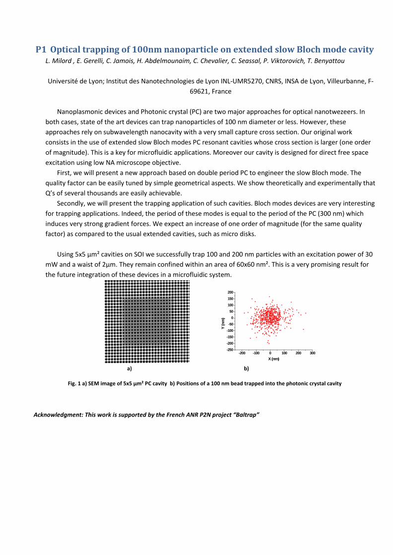
P1 Optical trapping of 100nm nanoparticle on extended slow Bloch mode cavity L. Milord , E. Gerelli, C. Jamois, H. Abdelmounaim, C. Chevalier, C. Seassal, P. Viktorovich, T. Benyattou Université de Lyon; Institut des Nanotechnologies de Lyon INL-UMR5270, CNRS, INSA de Lyon, Villeurbanne, F-
69621, France
Nanoplasmonic devices and Photonic crystal (PC) are two major approaches for optical nanotwezeers. In both cases, state of the art devices can trap nanoparticles of 100 nm diameter or less. However, these approaches rely on subwavelength nanocavity with a very small capture cross section. Our original work consists in the use of extended slow Bloch modes PC resonant cavities whose cross section is larger (one order of magnitude). This is a key for microfluidic applications. Moreover our cavity is designed for direct free space excitation using low NA microscope objective.
First, we will present a new approach based on double period PC to engineer the slow Bloch mode. The quality factor can be easily tuned by simple geometrical aspects. We show theoretically and experimentally that Q’s of several thousands are easily achievable.
Secondly, we will present the trapping application of such cavities. Bloch modes devices are very interesting for trapping applications. Indeed, the period of these modes is equal to the period of the PC (300 nm) which induces very strong gradient forces. We expect an increase of one order of magnitude (for the same quality factor) as compared to the usual extended cavities, such as micro disks.
Using 5x5 µm² cavities on SOI we successfully trap 100 and 200 nm particles with an excitation power of 30
mW and a waist of 2µm. They remain confined within an area of 60x60 nm². This is a very promising result for the future integration of these devices in a microfluidic system.
a) b)
Fig. 1 a) SEM image of 5x5 µm² PC cavity b) Positions of a 100 nm bead trapped into the photonic crystal cavity
Acknowledgment: This work is supported by the French ANR P2N project “Baltrap”
-200 -100 0 100 200 300-250-200-150-100-50
050
100150200
Y (n
m)
X (nm)

P2 Porous-Silicon Photonics for Biosensing
Cécile Jamois1, Mohsen Erouel1, Emmanuel Gerelli1, Huanhuan Liu1, Abdelmounaim Harouri1, Taha Benyattou1, Régis Orobtchouk1,
Yann Chevolot2, Virginie Monnier2 and Eliane Souteyrand 2
1 Université de Lyon; Institut des Nanotechnologies de Lyon INL-UMR5270, CNRS, INSA de Lyon, Villeurbanne, F-69621, France
2 Université de Lyon; Institut des Nanotechnologies de Lyon INL-UMR5270, CNRS, Ecole Centrale de Lyon, Ecully, F-69134, France
The new requirements for environmental, food and health monitoring leads to a growing need for new types of sensors enabling fast, simple and reliable molecular analysis. Among such devices, optical biochips designed for label-free and multiple parallel sensing are of high interest for many applications such as cost-effective detection of specific illnesses via the evidence of biomarkers in body fluids. At INL, we aim at the realization of biochips which are compatible with external reading systems for laboratory analysis, such as scanners or microscopes. As illustrated in the figure below, the transducers consist of photonic devices excited at normal incidence and with strongly varying reflection/transmission behavior in presence of target biomolecules.
Porous silicon is a well-known material to realize optical sensors, due to the very large specific surface available for molecular interactions as well as the flexibility in sensor design resulting from the possible in-depth modulation of the porosity (i.e., the effective refractive index). Using a technological toolbox consisting of standard micro-structuring processes combined with silicon anodization, a large variety of porous-silicon based photonic devices with highly-interesting optical properties can be achieved.
Applications to biosensing require molecular grafting inside the micropores of the material, which is realized via amino-silane chemistry on slightly oxidized porous silicon. DNA hybridization is investigated as an example of biosensing event in the porous silicon photonic devices.
Illustration of photonic biosensor based on porous silicon.
[1] C. Jamois, C. Li, E. Gerelli, et al., New Concepts of Integrated Photonic Biosensors Based on Porous Silicon, Biosensors - Emerging Materials and Applications, Edited by Pier Andrea Serra, Intech, 265-290 (2011)
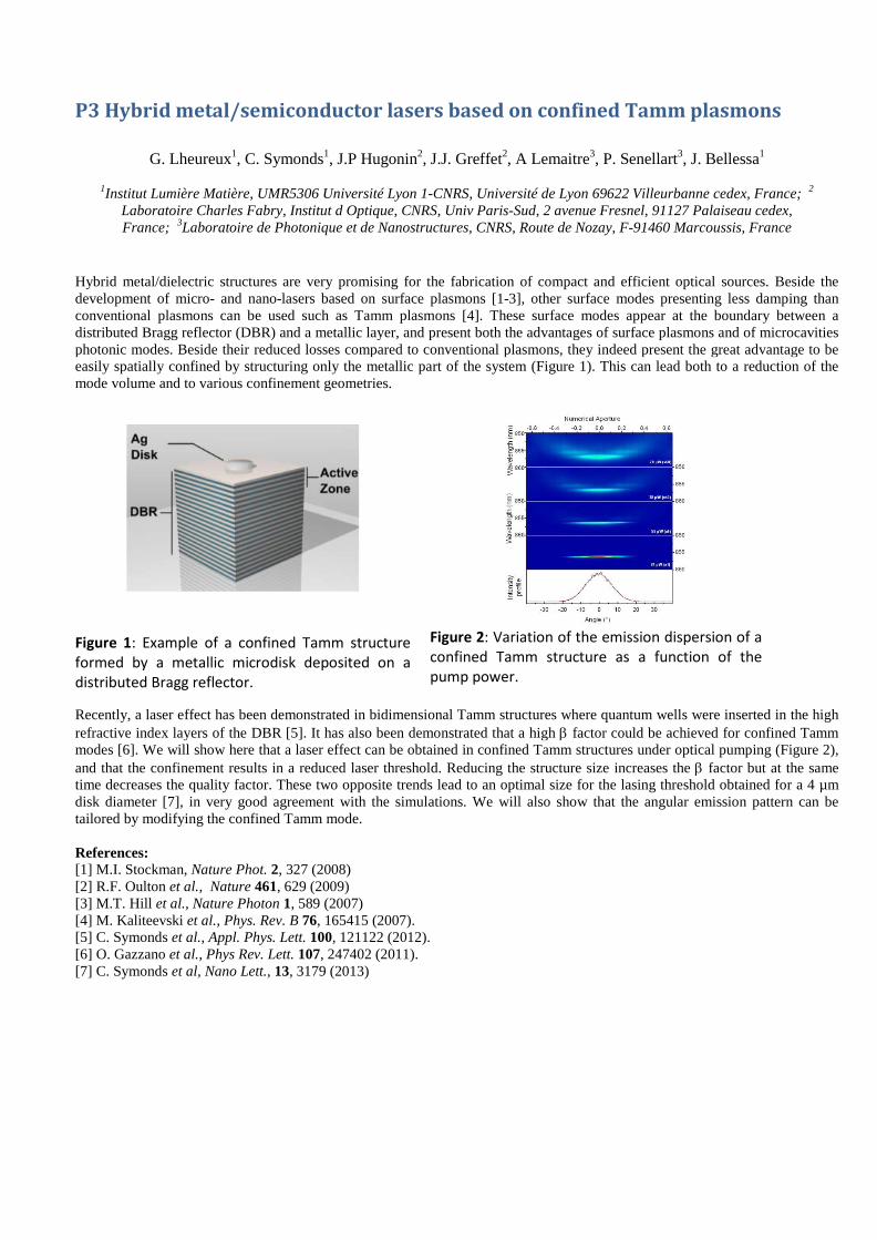
P3 Hybrid metal/semiconductor lasers based on confined Tamm plasmons
G. Lheureux1, C. Symonds1, J.P Hugonin2, J.J. Greffet2, A Lemaitre3, P. Senellart3, J. Bellessa1
1Institut Lumière Matière, UMR5306 Université Lyon 1-CNRS, Université de Lyon 69622 Villeurbanne cedex, France; 2 Laboratoire Charles Fabry, Institut d Optique, CNRS, Univ Paris-Sud, 2 avenue Fresnel, 91127 Palaiseau cedex, France; 3Laboratoire de Photonique et de Nanostructures, CNRS, Route de Nozay, F-91460 Marcoussis, France
Hybrid metal/dielectric structures are very promising for the fabrication of compact and efficient optical sources. Beside the development of micro- and nano-lasers based on surface plasmons [1-3], other surface modes presenting less damping than conventional plasmons can be used such as Tamm plasmons [4]. These surface modes appear at the boundary between a distributed Bragg reflector (DBR) and a metallic layer, and present both the advantages of surface plasmons and of microcavities photonic modes. Beside their reduced losses compared to conventional plasmons, they indeed present the great advantage to be easily spatially confined by structuring only the metallic part of the system (Figure 1). This can lead both to a reduction of the mode volume and to various confinement geometries.
Figure 1: Example of a confined Tamm structure formed by a metallic microdisk deposited on a distributed Bragg reflector.
Figure 2: Variation of the emission dispersion of a confined Tamm structure as a function of the pump power.
Recently, a laser effect has been demonstrated in bidimensional Tamm structures where quantum wells were inserted in the high refractive index layers of the DBR [5]. It has also been demonstrated that a high β factor could be achieved for confined Tamm modes [6]. We will show here that a laser effect can be obtained in confined Tamm structures under optical pumping (Figure 2), and that the confinement results in a reduced laser threshold. Reducing the structure size increases the β factor but at the same time decreases the quality factor. These two opposite trends lead to an optimal size for the lasing threshold obtained for a 4 µm disk diameter [7], in very good agreement with the simulations. We will also show that the angular emission pattern can be tailored by modifying the confined Tamm mode. References: [1] M.I. Stockman, Nature Phot. 2, 327 (2008) [2] R.F. Oulton et al., Nature 461, 629 (2009) [3] M.T. Hill et al., Nature Photon 1, 589 (2007) [4] M. Kaliteevski et al., Phys. Rev. B 76, 165415 (2007). [5] C. Symonds et al., Appl. Phys. Lett. 100, 121122 (2012). [6] O. Gazzano et al., Phys Rev. Lett. 107, 247402 (2011). [7] C. Symonds et al, Nano Lett., 13, 3179 (2013)

(a) Stimulated FWM Ps=1.3 µW
Pho
ton
Gen
erat
ion
rate
(Hz)
P4 SILICON-ON-INSULATOR COUPLED PHOTONIC WIRE NANO-CAVITIES: A PHOTONIC CRYSTAL MOLECULE FOR EFFICIENT FOUR-WAVE MIXING
Stefano Azzini1,§, Davide Grassani1, Matteo Galli1, Dario Gerace1, Maddalena Patrini1, Marco Liscidini1, Philippe Velha2, and Daniele Bajoni3
1Dipartimento di Fisica, Università degli Studi di Pavia, Pavia, Italy 2School of Engineering, University of Glasgow, Glasgow, United Kingdom; Istituto di Tecnologie della Comunicazione, Informazione e Percezione (TeCIP), Area CNR, Pisa, Italy 3Dipartimento di Ingegneria Industriale Informazione, Università degli Studi di Pavia, Pavia, Italy
The enhancement of optical nonlinearities is usually achieved by means of optical confinement, that allows
to increase the overlap between the electromagnetic field and the nonlinear material. In particular, photonic crystal (PhC) nano-cavities can confine light to volumes comparable to the cube of the wavelength in the material, offering the best enhancement of radiation-matter interaction among any dielectric nano-structure [1]. In this abstract, we report on the use of a novel PhC molecule (PCM) to obtain four-wave mixing (FWM) in a silicon-on-insulator (SOI) integrated device. In order to satisfy the energy conservation condition for FWM, three resonances are necessary for signal, pump and idler, evenly separated in energy. To this purpose, we exploit the natural splitting of the resonant modes of three identical side-coupled PhC nano- cavities [2]. Figure 1 shows an SEM image of our PCM [3]. This structure has been designed to be self-filtering in transmission with respect to the pump beam: if light is collected from the central cavity, a pump-power rejection of almost two orders of magnitude is measured at the output. The integrated emitted intensities for both stimulated and spontaneous FWM experiments performed on the device are reported in Figure 2, as a function of the pump power. The photon generation rate increases quadratically in both cases, as expected. In particular, a spontaneous generation rate of 1 MHz is obtained with a coupled pump power of about 50 μW, resulting in a conversion efficiency almost two orders of magnitude better than what reported for SOI micro-ring resonators [4]. This is physically due to the smaller volume of the PCM compared to other type of resonators, and makes this device a candidate for applications in ultra-low power non-linear optics and, potentially, SOI- integrated quantum optics.
Figura 1. Top-view scanning electron micrograph image of the SOI-integrated photonic crystal molecule.
107
106
105
(b) Spontaneous FWM
References.
[1] S. Strauf et al., Physical Review Letters 96, 2006 [2] C. Diederichs et al., Nature 440, 2006 [3] S.Azzini et al., Applied Physics Letters 103, 2013
10 100 Pump Power (µW)
104
signal idler
10 100 Pump Power (µW)
[4] S.Azzini et al., Optics Express 20(21), 2012; S.Clemmen et al., Optics Express 17(19), 2008
Figure 2. (a) Scaling of the estimated number of generated idler photons for stimulated FWM as a function of the pump power at a fixed signal power (the dashed lyne is a guide to the eye proportional to the square of the pump power). (b) Same for signal (black circles) and idler (white circles) photons for spontaneous FWM.
§ Present address: Institut Lumière Matière et Institut des Nanotechnologies de Lyon, Université de Lyon, Lyon, France
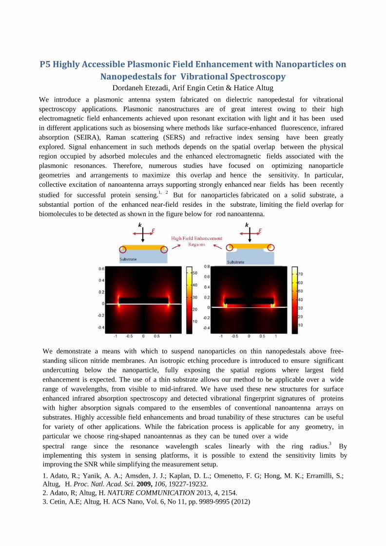
P5 Highly Accessible Plasmonic Field Enhancement with Nanoparticles on Nanopedestals for Vibrational Spectroscopy
Dordaneh Etezadi, Arif Engin Cetin & Hatice Altug We introduce a plasmonic antenna system fabricated on dielectric nanopedestal for vibrational spectroscopy applications. Plasmonic nanostructures are of great interest owing to their high electromagnetic field enhancements achieved upon resonant excitation with light and it has been used in different applications such as biosensing where methods like surface-enhanced fluorescence, infrared absorption (SEIRA), Raman scattering (SERS) and refractive index sensing have been greatly explored. Signal enhancement in such methods depends on the spatial overlap between the physical region occupied by adsorbed molecules and the enhanced electromagnetic fields associated with the plasmonic resonances. Therefore, numerous studies have focused on optimizing nanoparticle geometries and arrangements to maximize this overlap and hence the sensitivity. In particular, collective excitation of nanoantenna arrays supporting strongly enhanced near fields has been recently studied for successful protein sensing.1, 2 But for nanoparticles fabricated on a solid substrate, a substantial portion of the enhanced near-field resides in the substrate, limiting the field overlap for biomolecules to be detected as shown in the figure below for rod nanoantenna.
We demonstrate a means with which to suspend nanoparticles on thin nanopedestals above free- standing silicon nitride membranes. An isotropic etching procedure is introduced to ensure significant undercutting below the nanoparticle, fully exposing the spatial regions where largest field enhancement is expected. The use of a thin substrate allows our method to be applicable over a wide range of wavelengths, from visible to mid-infrared. We have used these new structures for surface enhanced infrared absorption spectroscopy and detected vibrational fingerprint signatures of proteins with higher absorption signals compared to the ensembles of conventional nanoantenna arrays on substrates. Highly accessible field enhancements and broad tunability of these structures can be useful for variety of other applications. While the fabrication process is applicable for any geometry, in particular we choose ring-shaped nanoantennas as they can be tuned over a wide spectral range since the resonance wavelength scales linearly with the ring radius.3 By implementing this system in sensing platforms, it is possible to extend the sensitivity limits by improving the SNR while simplifying the measurement setup. 1. Adato, R.; Yanik, A. A.; Amsden, J. J.; Kaplan, D. L.; Omenetto, F. G; Hong, M. K.; Erramilli, S.; Altug, H. Proc. Natl. Acad. Sci. 2009, 106, 19227-19232. 2. Adato, R; Altug, H. NATURE COMMUNICATION 2013, 4, 2154. 3. Cetin, A.E; Altug, H. ACS Nano, Vol. 6, No 11, pp. 9989-9995 (2012)
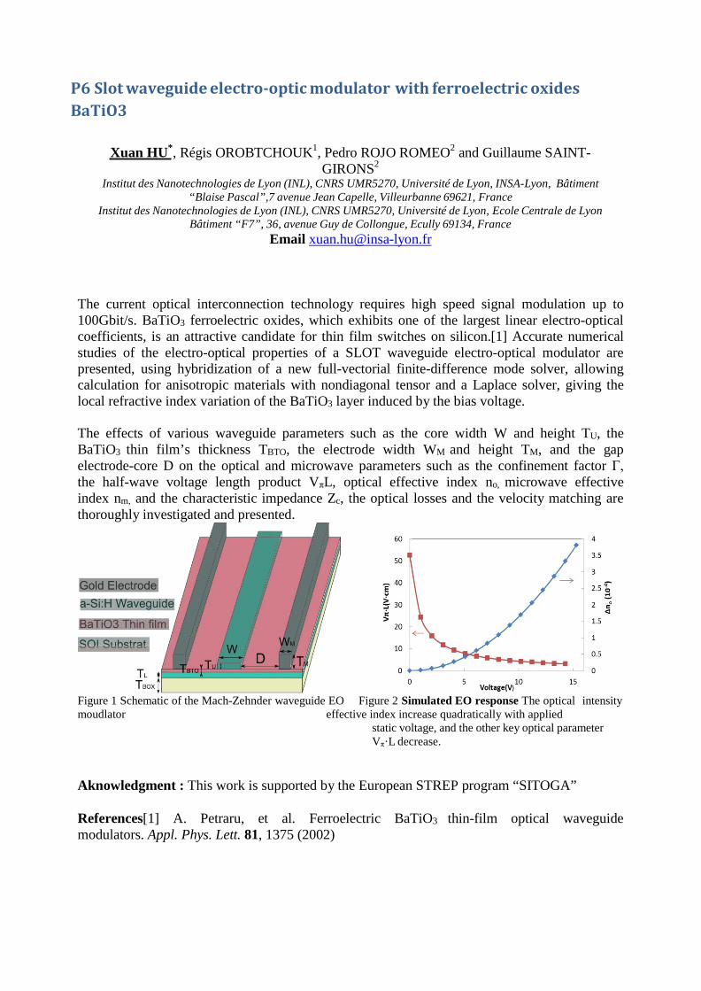
P6 Slot waveguide electro-optic modulator with ferroelectric oxides BaTiO3
Xuan HU*, Régis OROBTCHOUK1, Pedro ROJO ROMEO2 and Guillaume SAINT- GIRONS2
Institut des Nanotechnologies de Lyon (INL), CNRS UMR5270, Université de Lyon, INSA-Lyon, Bâtiment
“Blaise Pascal”,7 avenue Jean Capelle, Villeurbanne 69621, France Institut des Nanotechnologies de Lyon (INL), CNRS UMR5270, Université de Lyon, Ecole Centrale de Lyon
Bâtiment “F7”, 36, avenue Guy de Collongue, Ecully 69134, France Email [email protected]
The current optical interconnection technology requires high speed signal modulation up to 100Gbit/s. BaTiO3 ferroelectric oxides, which exhibits one of the largest linear electro-optical coefficients, is an attractive candidate for thin film switches on silicon.[1] Accurate numerical studies of the electro-optical properties of a SLOT waveguide electro-optical modulator are presented, using hybridization of a new full-vectorial finite-difference mode solver, allowing calculation for anisotropic materials with nondiagonal tensor and a Laplace solver, giving the local refractive index variation of the BaTiO3 layer induced by the bias voltage.
The effects of various waveguide parameters such as the core width W and height TU, the BaTiO3 thin film’s thickness TBTO, the electrode width WM and height TM, and the gap electrode-core D on the optical and microwave parameters such as the confinement factor Γ, the half-wave voltage length product VπL, optical effective index no, microwave effective index nm, and the characteristic impedance Zc, the optical losses and the velocity matching are thoroughly investigated and presented.
Figure 1 Schematic of the Mach-Zehnder waveguide EO Figure 2 Simulated EO response The optical intensity moudlator effective index increase quadratically with applied
static voltage, and the other key optical parameter Vπ·L decrease.
Aknowledgment : This work is supported by the European STREP program “SITOGA”
References[1] A. Petraru, et al. Ferroelectric BaTiO3 thin-film optical waveguide modulators. Appl. Phys. Lett. 81, 1375 (2002)

P7 Analysis of second order nonlinear effects in strained silicon
Pedro Damas, Xavier Le Roux, Eric Cassan, Delphine Marris-Morini, Nicolas Izard, Alain Bosseboeuf, Thomas Maroutian, Philippe Lecoeur, Laurent Vivien
Institut d’Electronique Fondamentale, Univ. Paris Sud, CNRS UMR 8622, 91405 Orsay Cedex [email protected]
Abstract: In this paper we propose a model to efficiently compare different structures for improvement of performance of strain-induced second order nonlinear effects in silicon devices, along with some preliminary experimental results based on Pockels effect.
Silicon-based photonics has generated a strong interest in recent years, mainly for optical telecommunications and optical interconnects in microelectronic circuits. The main rationales of silicon photonics are the reduction of photonic system costs and the increase of the number of functionalities on the same integrated chip by combining photonics and electronics [1].
In addition to be considered as the future photonic platform, silicon photonics is also a promising platform for a wide range of nonlinear optical processes due to its strong optical confinement and large nonlinearity. Indeed, nonlinear optics in silicon has been investigated as a potential mean to overcome electronic limitations in future information networks by easing all-optical signal processing. Several impressive works have been reported including wavelength and format conversions, signal regeneration, time-division demultiplexing, modulation instability, tunable delay [2].
However, bulk silicon possesses a crystalline symmetry (centro-symmetry) that inhibits the existence of nonzero elements in the second-order nonlinear susceptibility χ(2) tensor. It has indeed been recently demonstrated that this can be carried out by using a stress overlayer to induce strain in the silicon crystal underneath [3–5].
A further motivation for the use of second-order nonlinear effects induced by strain in silicon, is not only the possibility of harmonic generation (second harmonic generation, sum-frequency generation etc) in silicon devices but also the development of silicon optical modulators based on Pockels effect, whose speed would not be limited by charge mobility or charge recombination. Moreover, these effects are inherently driven at much lower power than those relying on third-order nonlinearities (Kerr effect) due to a quadratic field process for the latter.
In spite of these effects have already been developed and demonstrated [3–5], the understanding of the phenomena taking place due to the strain is far from being completely understood, leaving a large place for device optimization. In the present work we analyse the effects of strain in the silicon crystal which enables the nonvanishing χ(2) , we show how we can use that analysis to improve the second-order nonlinear effects along with the experimental verification of Pockels effect in strained SOI waveguides, where we used a SiN overlayer to generate the required stress in the silicon crystal lattice and then enable second order nonlinear phenomena.
References
1. J. M. Fedeli, L. D. Cioccio, D. Marris-Morini, L. Vivien, R. Orobtchouk, P. Rojo-Romeo, C. Seassal, and F. Mandorlo, “Development of silicon photonics devices using microelectronic tools for the integration on top of a cmos wafer.” Advances in Optical Technologies AOT, Special issue on ”Silicon Photonics” (2008).
2. J. Leuthold, C. AU Koos, and W. Freude, “Nonlinear silicon photonics,” Nature Photonics 4, 535 – 544 (2010). 3. R. S. Jacobsen, K. N. Andersen, P. I. Borel, J. Fage-Pedersen, L. H. Frandsen, O. Hansen, M. Kristensen, A.
V. Lavrinenko, G. Moulin, H. Ou, C. Peucheret, B. Zsigri, and A. Bjarklev, “Strained silicon as a new electro-optic material.” Nature 441, 199–202 (2006).
4. M. Cazzanelli, F. Bianco, E. Borga, G. Pucker, M. Ghulinyan, E. Degoli, E. Luppi, V. Veniard, S. Ossicini, D. Modotto, S. Wabnitz, R. Pierobon, and L. Pavesi, “Second-harmonic generation in silicon waveguides strained by silicon nitride.” Nature materials 11, 148–54 (2012).
5. B. Chmielak, M. Waldow, C. Matheisen, C. Ripperda, J. Bolten, T. Wahlbrink, M. Nagel, F. Merget, and H. Kurz, “Pockels effect based fully integrated, strained silicon electro-optic modulator.” Optics express 19, 17,212–9 (2011).
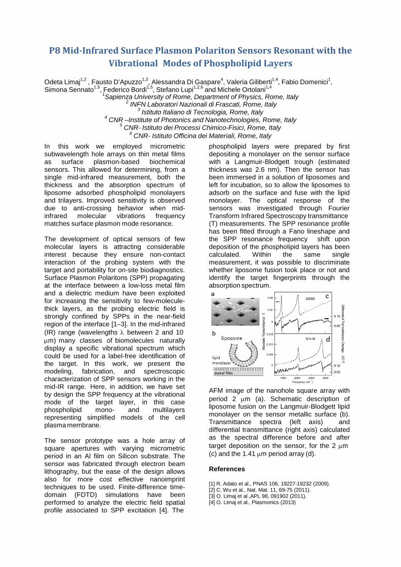
P8 Mid-Infrared Surface Plasmon Polariton Sensors Resonant with the Vibrational Modes of Phospholipid Layers
Odeta Limaj1,2 , Fausto D’Apuzzo1,3, Alessandra Di Gaspare4, Valeria Giliberti1,4, Fabio Domenici1, Simona Sennato1,5, Federico Bordi1,5, Stefano Lupi1,2,6 and Michele Ortolani1,4
1Sapienza University of Rome, Department of Physics, Rome, Italy
2 INFN Laboratori Nazionali di Frascati, Rome, Italy 3 Istituto Italiano di Tecnologia, Rome, Italy
4 CNR –Institute of Photonics and Nanotechnologies, Rome, Italy 5 CNR- Istituto dei Processi Chimico-Fisici, Rome, Italy
6 CNR- Istituto Officina dei Materiali, Rome, Italy In this work we employed micrometric subwavelength hole arrays on thin metal films as surface plasmon-based biochemical sensors. This allowed for determining, from a single mid-infrared measurement, both the thickness and the absorption spectrum of liposome adsorbed phospholipid monolayers and trilayers. Improved sensitivity is observed due to anti-crossing behavior when mid- infrared molecular vibrations frequency matches surface plasmon mode resonance.
The development of optical sensors of few molecular layers is attracting considerable interest because they ensure non-contact interaction of the probing system with the target and portability for on-site biodiagnostics. Surface Plasmon Polaritons (SPP) propagating at the interface between a low-loss metal film and a dielectric medium have been exploited for increasing the sensitivity to few-molecule- thick layers, as the probing electric field is strongly confined by SPPs in the near-field region of the interface [1–3]. In the mid-infrared (IR) range (wavelengths λ between 2 and 10 µm) many classes of biomolecules naturally display a specific vibrational spectrum which could be used for a label-free identification of the target. In this work, we present the modeling, fabrication, and spectroscopic characterization of SPP sensors working in the mid-IR range. Here, in addition, we have set by design the SPP frequency at the vibrational mode of the target layer, in this case phospholipid mono- and multilayers representing simplified models of the cell plasma membrane.
The sensor prototype was a hole array of square apertures with varying micrometric period in an Al film on Silicon substrate. The sensor was fabricated through electron beam lithography, but the ease of the design allows also for more cost effective nanoimprint techniques to be used. Finite-difference time- domain (FDTD) simulations have been performed to analyze the electric field spatial profile associated to SPP excitation [4]. The
phospholipid layers were prepared by first depositing a monolayer on the sensor surface with a Langmuir-Blodgett trough (estimated thickness was 2.6 nm). Then the sensor has been immersed in a solution of liposomes and left for incubation, so to allow the liposomes to adsorb on the surface and fuse with the lipid monolayer. The optical response of the sensors was investigated through Fourier Transform Infrared Spectroscopy transmittance (T) measurements. The SPP resonance profile has been fitted through a Fano lineshape and the SPP resonance frequency shift upon deposition of the phospholipid layers has been calculated. Within the same single measurement, it was possible to discriminate whether liposome fusion took place or not and identify the target fingerprints through the absorption spectrum.
AFM image of the nanohole square array with period 2 µm (a). Schematic description of liposome fusion on the Langmuir-Blodgett lipid monolayer on the sensor metallic surface (b). Transmittance spectra (left axis) and differential transmittance (right axis) calculated as the spectral difference before and after target deposition on the sensor, for the 2 µm (c) and the 1.41 µm period array (d).
References
[1] R. Adato et al., PNAS 106, 19227-19232 (2009). [2] C. Wu et al., Nat. Mat. 11, 69-75 (2011). [3] O. Limaj et al.,APL 98, 091902 (2011). [4] O. Limaj et al., Plasmonics (2013)
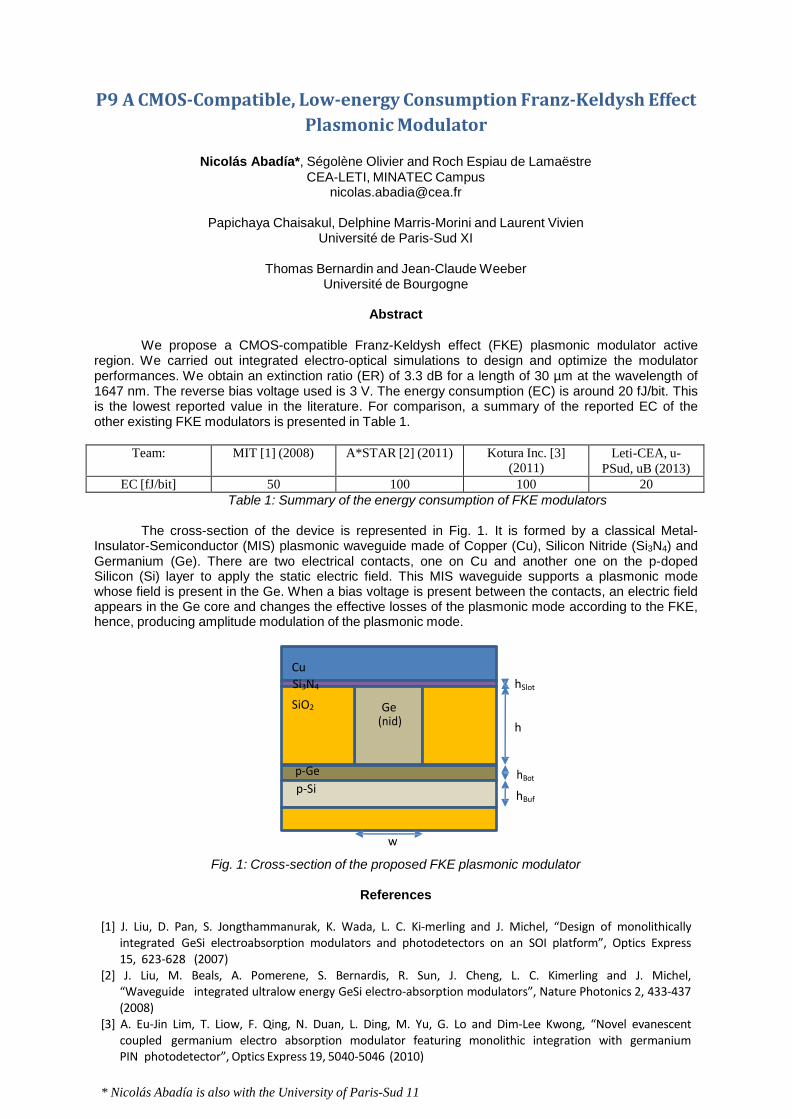
P9 A CMOS-Compatible, Low-energy Consumption Franz-Keldysh Effect Plasmonic Modulator
Nicolás Abadía*, Ségolène Olivier and Roch Espiau de Lamaëstre
CEA-LETI, MINATEC Campus [email protected]
Papichaya Chaisakul, Delphine Marris-Morini and Laurent Vivien
Université de Paris-Sud XI
Thomas Bernardin and Jean-Claude Weeber Université de Bourgogne
Abstract
We propose a CMOS-compatible Franz-Keldysh effect (FKE) plasmonic modulator active
region. We carried out integrated electro-optical simulations to design and optimize the modulator performances. We obtain an extinction ratio (ER) of 3.3 dB for a length of 30 µm at the wavelength of 1647 nm. The reverse bias voltage used is 3 V. The energy consumption (EC) is around 20 fJ/bit. This is the lowest reported value in the literature. For comparison, a summary of the reported EC of the other existing FKE modulators is presented in Table 1.
Team: MIT [1] (2008) A*STAR [2] (2011) Kotura Inc. [3]
(2011) Leti-CEA, u-
PSud, uB (2013) EC [fJ/bit] 50 100 100 20
Table 1: Summary of the energy consumption of FKE modulators
The cross-section of the device is represented in Fig. 1. It is formed by a classical Metal- Insulator-Semiconductor (MIS) plasmonic waveguide made of Copper (Cu), Silicon Nitride (Si3N4) and Germanium (Ge). There are two electrical contacts, one on Cu and another one on the p-doped Silicon (Si) layer to apply the static electric field. This MIS waveguide supports a plasmonic mode whose field is present in the Ge. When a bias voltage is present between the contacts, an electric field appears in the Ge core and changes the effective losses of the plasmonic mode according to the FKE, hence, producing amplitude modulation of the plasmonic mode.
Cu Si3N4
SiO2 Ge (nid)
hSlot
h
p-Ge p-Si
hBot
hBuf
w
Fig. 1: Cross-section of the proposed FKE plasmonic modulator
References
[1] J. Liu, D. Pan, S. Jongthammanurak, K. Wada, L. C. Ki-merling and J. Michel, “Design of monolithically integrated GeSi electroabsorption modulators and photodetectors on an SOI platform”, Optics Express 15, 623-628 (2007)
[2] J. Liu, M. Beals, A. Pomerene, S. Bernardis, R. Sun, J. Cheng, L. C. Kimerling and J. Michel, “Waveguide integrated ultralow energy GeSi electro-absorption modulators”, Nature Photonics 2, 433-437 (2008)
[3] A. Eu-Jin Lim, T. Liow, F. Qing, N. Duan, L. Ding, M. Yu, G. Lo and Dim-Lee Kwong, “Novel evanescent coupled germanium electro absorption modulator featuring monolithic integration with germanium PIN photodetector”, Optics Express 19, 5040-5046 (2010)
* Nicolás Abadía is also with the University of Paris-Sud 11

P 10 Absorption Spectroscopy of Structure-Identified Individual Single-Wall Carbon Nanotubes
1* 2 2 2 2 1 1 J.-C. Blancon , M. Paillet , H.-N. Tran , D. Levshov , X. T. Than , S. Aberra Guebrou , A. Ayari ,
1 2 2 1 1 A. San Miguel , A. A. Zahab , J.-L. Sauvajol , N. Del Fatti , F. Vallée
1. Institut Lumière Matière, UMR5306 Université Lyon 1-CNRS, Université de Lyon 69622 Villeurbanne cedex, France. 2. Laboratoire Charles Coulomb UMR 5221, Université Montpellier 2-CNRS, Montpellier, France.
The unique optical and electronic properties of single-wall carbon nanotubes (SWNTs) are appealing for the development of novel applications in optoelectronics, solar cells and sensor systems.1 Despite the large amount of data collected with photoluminescence, Raman spectroscopy and Rayleigh scattering, knowledge the intrinsic absorption characteristics of these nano-objects is still partial. The understanding of absorption processes occurring in different types of carbon nanotubes is crucial, and more precisely this comprehension should occur at the individual nanotube level. Values of absorption cross-section were reported using photoluminescence and Rayleigh scattering, but are indirect measurements requiring hypotheses on the absorption processes taking place in carbon nanotubes.
Here we present direct measurements of the absolute absorption cross-section of individual carbon nanotubes using the spatial modulation spectroscopy technique developed in our lab (Figure 1).2 We obtained the first broadband polarized absorption spectra of individual SWNTs either free-standing or in the presence of subject to an external environment (Figure 1).3 The optical absorption properties were investigated regarding the nanotubes structural characteristics (obtained via absorption and Raman spectroscopy) and their environment (e.g. supported on a substrate). Clear modifications of the light-matter interactions were observed depending on the structure and environment of the SWNTs, as shown through energy shifts and broadenings of the excitonic resonance peaks as well as weakening of antenna effects.
Figure 1. (Left-middle panels) Far-field absorption-based optical imaging of individual single-wall carbon nanotubes obtained with spatial modulation spectroscopy. (Right panel) Broadband absorption cross-section spectrum of a freely suspended individual SWNT identified as semiconducting with associated diameter 2.0 nm and chirality (22,6). For more details, see refs. [2,3].
References [1] P. Avouris, M. Freitag, and V. Perebeinos, Nature Photonics 2, 341 (2008). [2] D. Christofilos, J.-C. Blancon, J. Arvanitidis, et al., Journal of Physical Chemistry Letters 3, 1176 (2012). [3] J.-C. Blancon, M. Paillet, H. N. Tran et al., Nature Communications 4:2542 (2013).
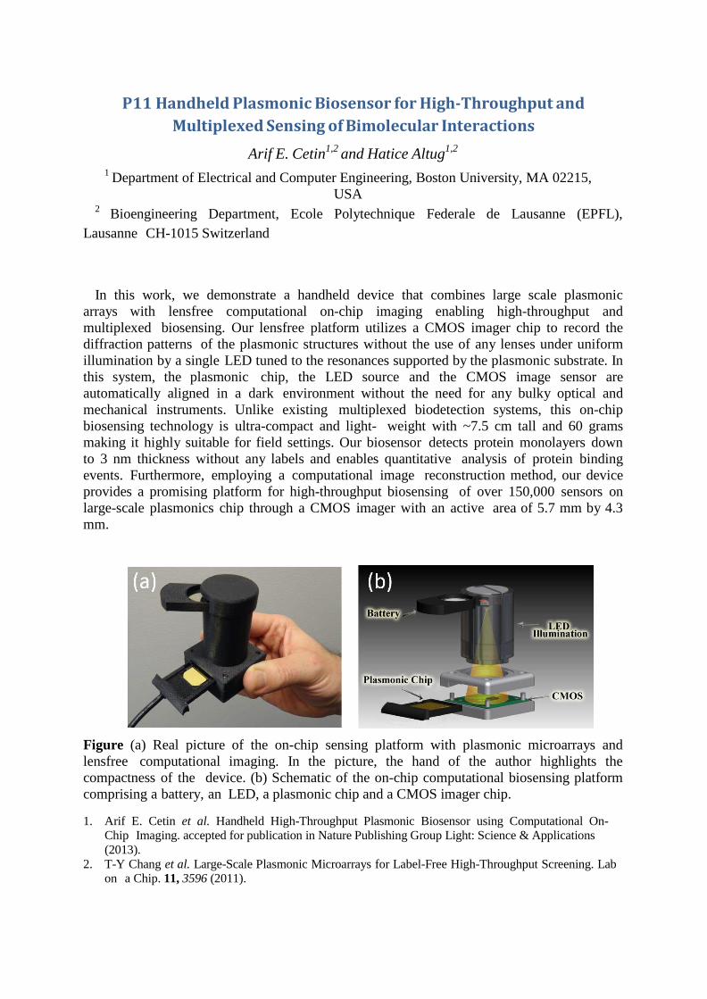
P11 Handheld Plasmonic Biosensor for High-Throughput and Multiplexed Sensing of Bimolecular Interactions
Arif E. Cetin1,2 and Hatice Altug1,2
1 Department of Electrical and Computer Engineering, Boston University, MA 02215, USA
2 Bioengineering Department, Ecole Polytechnique Federale de Lausanne (EPFL), Lausanne CH-1015 Switzerland
In this work, we demonstrate a handheld device that combines large scale plasmonic arrays with lensfree computational on-chip imaging enabling high-throughput and multiplexed biosensing. Our lensfree platform utilizes a CMOS imager chip to record the diffraction patterns of the plasmonic structures without the use of any lenses under uniform illumination by a single LED tuned to the resonances supported by the plasmonic substrate. In this system, the plasmonic chip, the LED source and the CMOS image sensor are automatically aligned in a dark environment without the need for any bulky optical and mechanical instruments. Unlike existing multiplexed biodetection systems, this on-chip biosensing technology is ultra-compact and light- weight with ~7.5 cm tall and 60 grams making it highly suitable for field settings. Our biosensor detects protein monolayers down to 3 nm thickness without any labels and enables quantitative analysis of protein binding events. Furthermore, employing a computational image reconstruction method, our device provides a promising platform for high-throughput biosensing of over 150,000 sensors on large-scale plasmonics chip through a CMOS imager with an active area of 5.7 mm by 4.3 mm.
Figure (a) Real picture of the on-chip sensing platform with plasmonic microarrays and lensfree computational imaging. In the picture, the hand of the author highlights the compactness of the device. (b) Schematic of the on-chip computational biosensing platform comprising a battery, an LED, a plasmonic chip and a CMOS imager chip.
1. Arif E. Cetin et al. Handheld High-Throughput Plasmonic Biosensor using Computational On-Chip Imaging. accepted for publication in Nature Publishing Group Light: Science & Applications (2013).
2. T-Y Chang et al. Large-Scale Plasmonic Microarrays for Label-Free High-Throughput Screening. Lab on a Chip. 11, 3596 (2011).

P12 Angulo-spectral plasmonic properties of nano-micro-structured sensing substrates
Maha Chamtouri, Mitradeep Sarkar, Alexandra Sereda, Mondher Besbes,
Anne-Lise Coutrot, Julien Moreau, Michael Canva
Laboratoire Charles Fabry, Institut d’Optique Graduate School, Université Paris Sud, CNRS
2 avenue Augustin Fresnel, 91127 Palaiseau, France [email protected]
Surface Plasmon Resonance (SPR) biosensors are currently standard tools for label free and
real time detection of biomolecular interactions. Biochip systems based on SPR, using metallic thin films, have limited performance for ultra-low concentration probing. With the perspective of surpassing this limitation, we have extensively investigated the optical properties of nano-micro 2D metallic gratings. The studied structures consist of an array of metallic ribbons structured on a metallic film, ideal for studying both propagating and localized plasmonic modes as well as hybrid modes resulting from their interactions. Understanding such plasmonic modes allows the control of the tailored biochip response for a wide range of sensing applications.
Theoretical simulations are performed by means of specifically developed codes, based on
the combination of the Finite Elements Method and Fourier Modal Method (FEM+FMM). Prototype samples are realized with e-beam lithography. Using an angulo-spectral SPR imaging system, it is possible to measure experimentally the reflectivity maps for several excitation angles and wavelengths. Multiple structured zones on a chip with different geometrical parameters can be simultaneously characterized and compared to simulations as illustrated for a selected configuration in Figure 1. This allows the direct visualization of plasmonic modes and their dispersion as well as the presence of plasmonic band-gaps caused by the Bragg Scattering phenomena. We have studied the band gap position dependency with the structure size and spacing dimensions in the nano and micro scale. Plasmonic sensing capabilities of these structures, were quantified in term of reflectivity variation and measured both for step index (in “% /RIU” (Refractive Index Unit)) and thickness of bio-layers binding to the structure (in “% / nm”).
Fig. 1 Reflectivity maps of 2D grating with ribbon size of 1µM and spacing of 400nm (a) simulation (b) Experiment

P13 Fabrication and characterization of ultra-short lithium niobate photonic crystals with giant aspect ratios
C. Guyot1, G. Ulliac1, J. Dahdah2, W. Qiu1, M.-P. Bernal1, F. Baida1, N. Courjal1 1 : Institut FEMT-ST, 16 route de Gray, 25030 Besançon cedex, France
2 : Kapteos, 23 avenue du Lac Léman, BP 347, 73377 Le Bourget-du-Lac cedex, France nadege.courjal@femto-
st.fr The development of all-optical, acousto-optical or electro-optical photonic crystals (PhCs) represents a stimulating
challenge for the production of advanced functionalities in compact optical devices. LiNbO3 appears to be an excellent candidate for such realizations, due to its well-known nonlinear, piezoelectric and electro-optic properties. Two major techniques exist to write PhCs on LiNbO3 waveguides: the first one involves the modification of lattices (by photorefraction or proton exchange). But this technique doesn't induce a sufficient index contrast (n<0,01)and PhCs need to be several millimeter long to warrant reflection coefficients over 90% in optical resonators [1,2]. Those distances should now be drastically reduced to facilitate the production of integrated LiNbO3 components. Zhou et al. proposed recently to increase the index contrast in including 1D PhC made by photorefraction on LiNbO3 thin films. It allowed a reflectivity of 50 % for a PhC length of only 175 µm [3]. Another technique relying on dry etching (by Focused Ion Beam milling or femtosecond laser writing) allows to have a better index contrast. However, LiF redeposition limits the possibilities to create high aspect ratio nanostructures, which could cover the entire optical mode. We propose here easy-to-implement techniques to reduce considerably 1D PhC length to a few micrometers in keeping a 50 % reflection for both polarizations. In combining a circular precision saw and Focused Ion Beam (FIB) milling, we are able to fabricate confined ridge waveguides with low propagation losses and high aspect ratios photonic crystals, which increases the interaction between optical modes and the crystal, and thus allows the reduction of the active lengths.
The first step of fabrication consists in creating a planar waveguide by titanium indiffusion or proton exchange. Then, a ridge waveguide is cut in the substrate with a circular precision saw (DISCO-DAD 3350) to confine the optical modes laterally (Fig. 1.a). This technique, which cuts and polishes simultaneously, allows to make giant aspect ratio ridge waveguides (>500) with propagation losses lower than 1 dB/cm [4]. The last step consists in the fabrication of a high aspect ratio photonic crystal by FIB milling the top and/or the lateral sides of the ridge, as shown in Fig. 1.b and 1.c.
(a) (b) (c) Figure 1. (a) Ridge waveguide cut with a circular saw (b) Bragg grating etched by FIB milling on top of a ridge.
(c) High aspect ratio 2D photonic crystal etched by FIB milling on top of a ridge.
A 8 µm long Bragg grating (1D PhC), with a period of 1690 nm (Fig. 1.b) was optically characterized. The reflectivity of such mirror is expected to be as high as 99.7%. A broadband source between 1525 and 1570 nm is injected in the ridge with an amplified spontaneous emission (ASE) laser. Transmission and reflection through the ridge waveguide was measured with a high-resolution optical spectrum analyzer (APEX). From the Fourier transforms of the different spectra, we determine the group index, reflection coefficients and propagation losses for both polarizations. The experimental reflectivity of the grating was estimated to be 48 ± 1 % for TE mode and 53 ± 2 % for TM mode. Numerical simulation by 2D-FDTD (Finite Difference Time Domain) was performed considering the sidewall angle of the grating layers. For such grating, the theoretical reflection coefficients become 46% for TE mode and 50% for TM mode. More details of the fabrication process and of the characterization of high aspect ratio photonic crystals in LiNbO3 will be given during the conference.
This work was financed by the ANR project “Mat. et Procédés pour les Produits Innovants” 2012 (CHARADES), by the region of Franche-Comté, et by the DGA RAPID project “SNIFER".
References [1] B.-E. Benkelfat, R. Ferrière, B. Wacogne, et al, "Technological implementation of Bragg grating reflectors in Ti:LiNbO3 waveguides by proton exchange", IEEE Phot. and Technol. Lett., 14, pp. 1430-1432, 2002. [2] D. Noriega Urquidez, S. Stepanov, H. Soto Ortiz, et al, "Electrically controlled slow/fast propagation of 12.5-GHz light pulses in lithium niobate waveguide Bragg grating", Appl. Phys. B vol. 106, pp. 51-56, 2012. [3] Z. Zhou, X. Huang, R. Rao Vanga, Z. Wu, "Enhanced photonic bandgap in ion-implanted lithium niobate waveguides by improving index contrast", JOSA B, vol. 27, pp. 1425-1429, 2010. [4] N. Courjal, B. Guichardaz, G. Ulliac, J.-Y. Rauch, B. Sadani, H.-H. Lu, and M.-P. Bernal, "High aspect ratio lithium niobate ridge waveguides fabricated by optical grade dicing", J. Phys. D: Appl. Phys., Vol. 44, 305101 (2011)
30 µm
ridge
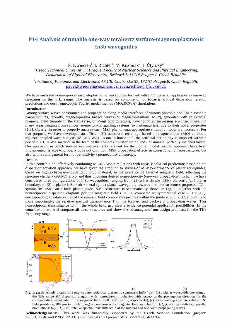
P14 Analysis of tunable one-way terahertz surface-magnetoplasmonic InSb waveguides
P. Kwiecien1, I. Richter1, V. Kuzmiak2, J. Čtyroký2
1 Czech Technical University in Prague, Faculty of Nuclear Sciences and Physical Engineering, Department of Physical Electronics, Břehová 7, 11519 Prague 1, Czech Republic
2Institute of Photonics and Electronics AS CR, Chaberská 57, 182 51 Prague 8, Czech Republic [email protected], [email protected]
We have analyzed nonreciprocal magnetoplasmonic waveguides formed with InSb material, applicable as one-way structures in the THz range. The analysis is based on combination of (quasi)analytical dispersion relation predictions and our magnetooptic Fourier modal method (MOaRCWA) simulations. Introduction Among surface waves constrained and propagating along media interfaces of various photonic and / or plasmonic nanostructures, recently, magnetoplasma surface waves (or magnetoplasmons, MSP), generated with an external magnetic field (mainly in the transverse, or Voigt configuration), have found an increasing scientific interest in many areas ranging from sensors, nonreciprocal guiding systems, to metamaterials, due to their novel properties [1,2]. Clearly, in order to properly analyze such MSP phenomena, appropriate simulation tools are necessary. For that purpose, we have developed an efficient 2D numerical technique based on magnetooptic (MO) aperiodic rigorous coupled wave analysis (MOaRCWA). In our in-house tool, the artificial periodicity is imposed within a periodic 1D RCWA method, in the form of the complex transformation and / or uniaxial perfectly matched layers. Our approach, in which several key improvements relevant for the Fourier modal method approach have been implemented, is able to properly cope not only with MSP propagation effects in corresponding nanostructures, but also with a fully general form of permittivity / permeability anisotropy. Results In this contribution, effectively combining MOaRCWA simulations with (quasi)analytical predictions based on the dispersion equation approach, we have given the attention to studies of MSP performance of planar waveguides, based on highly-dispersive polaritonic InSb material, in the presence of external magnetic field, affecting the structure via the Voigt MO effect and thus imposing desired nonreciprocity (one-way propagation). In fact, we have considered three configurations of InSb waveguides, ranging from: (1) a flat simple InSb / dielectric (air) planar boundary, to (2) a planar InSb / air / metal (gold) planar waveguide, towards the new structures proposed, (3) a symmetric InSb / air / InSb planar guide. Such structures is schematically shown in Fig. 1, together with the nonreciprocal dispersion diagram (for the magnetic field B = 1T, compared to symmetrical case – B = -1T), corresponding absolute values of the relevant field components profiles within the guide structure (Hy shown), and most importantly, the relative spectral transmittance T of the forward and backward propagating waves. This nonreciprocal transmittance within the whole band gap clearly evidence potential application possibilities. In the contribution, we will compare all three structures and show the advantages of our design proposed for the THz frequency range.
(a) (b) (c) (d) Fig. 1: (a) Schematic picture of a one-way nonreciprocal plasmonic symmetric InSb / air / InSb planar waveguide operating at
the THz range; (b) dispersion diagram with nonreciprocity behavior with respect to the propagation direction for the corresponding waveguide for the magnetic field B = 0T and B = 1T, respectively); (c) corresponding absolute values of Hy field profiles @280 µm (= 0.532 ω/ωp) – comparison for magnetic field switched off (Hy,0), and on (with two parallel orientations: Hy,+ , Hy,-); (d) relative spectral transmittance T of the forward and backward propagating waves.
Acknowledgements: This work was financially supported by the Czech Science Foundation (projects P205/10/0046 and P205/12/G118) and internal CTU project SGS13/221/OHK4/3T/14.
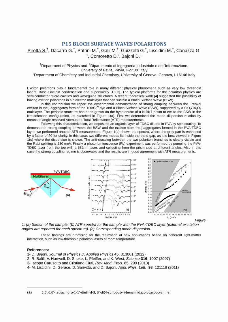
P15 BLOCH SURFACE WAVES POLARITONS Pirotta S.†, Dacarro G.†, Patrini M.†, Galli M.†, Guizzetti G.†, Liscidini M.†, Canazza G.
♢, Comoretto D.♢, Bajoni D.‡
†Department of Physics and ‡Dipartimento di Ingegneria Industriale e dell'Informazione, University of Pavia, Pavia, I-27100 Italy
♢Department of Chemistry and Industrial Chemistry, University of Genova, Genova, I-16146 Italy
Exciton polaritons play a fundamental role in many different physical phenomena such as very low threshold lasers, Bose-Einstein condensation and superfluidity [1,2,3]. The typical platforms for the polariton physics are semiconductor micro-cavities and waveguide structures. A recent theoretical work [4] suggested the possibility of having exciton polaritons in a dielectric multilayer that can sustain a Bloch Surface Wave (BSW). In this contribution we report the experimental demonstration of strong coupling between the Frenkel exciton in the j-aggregates form of the TDBC(a) dye and a Bloch Surface Wave (BSW), supported by a SiO2/Ta2O5 multilayer. The periodic structure has been grown on the hypotenuse of a N-BK7 prism to excite the BSW in the Krestchmann configuration, as sketched in Figure 1(a). First we determined the mode dispersion relation by means of angle-resolved Attenuated Total Reflectance (ATR) measurements. Following this characterization, we deposited an organic layer of TDBC diluted in PVA by spin coating. To demonstrate strong coupling between the BSW and the exciton from the j-aggregates formed in the PVA-TDBC layer, we performed another ATR measurement: Figure 1(b) shows the spectra, where the grey part is enhanced by a factor of 20 for clarity. In this case, two different modes lie inside the band gap, as it is best-viewed in Figure 1(c) where the dispersion is shown. The anti-crossing between the two polariton branches is clearly visible and the Rabi splitting is 280 meV. Finally a photo-luminescence (PL) experiment was performed by pumping the PVA-TDBC layer from the top with a 532nm laser, and collecting from the prism side at different angles. Also in this case the strong coupling regime is observable and the results are in good agreement with ATR measurements.
These findings are promising for the realization of new applications based on coherent light-matter interaction, such as low-threshold polariton lasers at room temperature.
References: 1- D. Bajoni, Journal of Physics D: Applied Physics 45, 313001 (2012) 2- R. Balili, V. Hartwell, D. Snoke, L. Pfeiffer, and K. West, Science 316, 1007 (2007) 3- Iacopo Carusotto and Cristiano Ciuti, Rev. Mod. Phys. 85, 299 (2013) 4- M. Liscidini, D. Gerace, D. Sanvitto, and D. Bajoni, Appl. Phys. Lett. 98, 121118 (2011)
(a) 5,5’,6,6’-tetrachloro-1-1’-diethyl-3, 3’-di(4-sulfobutyl)-benzimidazolocarbocyanine
Figure 1: (a) Sketch of the sample. (b) ATR spectra for the sample with the PVA-TDBC layer (external excitation angles are reported for each spectrum). (c) Corresponding mode dispersion.
P16 Pulsed Laser Deposition for research of innovative phosphor nanostructure made from Al and Ag
N. Abdellaoui1*, A. Pereira1, G. Colas des Francs2, A. Berthelot1, B. Moine1, A. Pillonnet1
1) Institut Lumière Matière, UMR5306 Université Lyon 1-CNRS, 69622 Villeurbanne cedex, France
2) ICB - Université de Bourgogne, CNRS UMR5209, Dijon 21078, France
*corresponding author : [email protected], tel.: +33 472 432 971, fax : +33 472 431 130
Pulsed laser deposition (PLD) is an efficient method for innovated composite material research, as mixed architectures made of plasmonic structure and phosphor. Theoretical studies on these plasmonic structures show promising results for many potential applications such as colored displays, optical telecommunication fibers or photovoltaic spectral conversion layer. However the experimental observations of the effects on phosphor made of rare earth emitters are scarce. This research needs to control at the nanoscale level the size and the shape of the metallic nanostructures, as well as the distance between the emitter and the metal. PLD is a suitable method for the controlled design of structured multilayers. This technique allows the deposition in a single step, guarantees a high quality of the interfaces and prevents any reactivity of the embedded metallic structures with ambiant atmosphere. Moreover the adjustment of thickness could be realized at the nanoscale. In this presentation, we propose to compile our results on the plasmonic effects on red Eu:Y2O3 phosphor. Two kinds of metal, Ag and Al, has been used to adjust the plasmon resonance to the absorption of Eu3+ ions in blue f-f dipolar electric transition or in UV Eu-O transfer charge respectively [1]. The effects of the spacer, the shape of metal (isolated nanoparticles, nanoresonator and mirror) are presented. Our structures are modeled to understand the mechanisms involved in the observed emission enhancement and to optimize the future design. [1] A. Pillonnet, A. Berthelot, A. Pereira, O. Benamara, S. Derom, G. Colas Des Francs, A.M. Jurdyc, Appl. Phys. Lett. 100, 153115 (2012)

P17 Complex photonic crystals structure to enhance optical light trapping in thin film 2nd generation solar cells
L. Lalouat*, R. Peretti, X. Meng, G. Gomard, S. Seassal, E. Drouard
Université de Lyon; Institut des Nanotechnologies de Lyon INL-UMR5270,CNRS Ecole Centrale de Lyon, Ecully, France
The efficiency of 2nd generation solar cells, constituted of thin absorbing layers, is limited by both the absorption efficiency and carrier recombination issues. Integrating novel light trapping schemes enables the optimization of the absorption efficiency in the active layers with a strongly reduced thickness, which could also lead to a higher carrier collection efficiency. Different kinds of structures can be used to enhance the absorption in the active layer [1]. We will focus us on dielectric photonic crystal (PC) as depicted in Fig.1a. For instance, by adding a square lattice of cylindrical holes at the top of a 1µm thick layer of crystalline silicon (c-Si), the absorption of this layer can be increased by 50% [2].
In this communication, we will discuss on the properties of complex PC structure for the control of sunlight absorption. We investigated two kind of complex PC: double-side PC (as shown in Fig.1b) and multi-periodic PC. In the first case (double-side two-dimensional PC), we will show that the sunlight absorption of a 1µm c-Si can be increased up to 65% compared to the absorption of the multilayer case [3].
In the case of multi-periodic PC, the second periodicity of the system enables to increase the usefull absorption of the system (+2% in absolute compared to an optimized mono-periodic PC) in order the beat the lambertian limit (+1% in absolute) [4]. It can be noted that the sunlight absorption can be further increased by using an anti-reflecting coating on the top of our structure.
Fig. 1: (a) Schematic view of a photonic crystal solar cell. (b) Example of 1D double-side photonic crystal
structure. [1] S. Mokkapati, K.R. Catchpole, Journal of Applied Physics, vol. 112, no. 10, p. 101101, 2012 [2] X. Meng et al, Optics Express, vol. 20, no. S4, pp A465-475, 2012 [3] X. Meng et al, Optics Express, vol. 20, no. 5, pp. A560-571, 2012 [4] R. Peretti et al, submitted to Physical Review A

P18 Plasmonic slot waveguide couplers - comparison of linear and nonlinear regimes
J. Petráček1, P. Kwiecien2, I. Richter2
1Institute of Physical Engineering, Faculty of Mechanical Engineering, Brno University of Technology, Technická 2, 616 69 Brno, Czech Republic
2Czech Technical University in Prague, Faculty of Nuclear Sciences and Physical Engineering, Department of Physical Electronics, Břehová 7, 11519 Prague 1, Czech Republic
[email protected], [email protected], [email protected]
In our study, we have numerically investigated nonlinear switching in plasmonic directional couplers consisting of two dielectric slab waveguides separated with metallic claddings, in terms of their geometrical as well as physical parameters. The analysis is based on an effective extension of the eigenmode expansion (EME) method, NL-EME, by using the rigorous coupled-mode theory. The simulations are confirmed with nonlinear finite difference time domain (FDTD) technique. Introduction Among photonic guiding structures, recently, plasmonic waveguides [1] of various geometries and configurations, ranging from slot, dielectrically-loaded, and hybrid platforms, have found an increasing scientific interest in many application areas, due to their subwavelength confinement and ability to light manipulation at the nanoscale. Even considering only planar structures, i.e. plasmonic slot waveguides, represented with a dielectric core guide, surrounded with metallic slabs, have already shown effective functioning. Since all plasmonic materials suffer from their (metallic) losses, there is always an inherent trade-off between confinement and propagation characteristics [1,2]. A very attractive feature of plasmonic devices is that they strongly increase local electromagnetic fields. Thus, nonlinear optical effects, which are inherently weak, can be significantly enhanced in plasmonic devices. This can be exploited in many potential applications [3]. Here we consider Kerr-nonlinearity (i.e. intensity dependent refractive index) which, in conjunction with plasmonics, can enable fabrication of miniature all-optical functional devices, such as switches, gates or memories. Results In this contribution, based on the effective combination of the rigorous coupled-mode theory with EME technique (NL- EME), we have given the primary attention to plasmonic directional couplers, as the one shown in Fig. 1a). These structures can serve as important elements in many nanooptical circuits since they can realize both coupling between plasmonic and dielectric waveguides, as well as between plasmonic waveguides only. Clearly, based on our recent study [4], understanding of the physics of such a device, comparing both linear and nonlinear (with Kerr nonlinearity, i.e. with intensity), is a very important issue. Therefore, first, we have studied the operation of the coupler in the linear regime since it further affects the nonlinear functionality, and compared both regimes. Such a structure under investigation is schematically shown in Fig. 1, together with the relative output power distributions, depending on an increasing nonlinearity (Fig. 1b). Also, we have studied the power-dependent switching characteristics of the relative output power with respect to the level of nonlinearity (Fig. 1c). We have taken into account the nonlinearities of both dielectric as well as metal. We have also looked at the effect of realistic losses present in real materials, especially metals. Using our technique, we have demonstrated how the switching characteristics can, in fact, be improved by varying both geometrical (i.e. waveguide width and separation) as well as material parameters (e.g. silicon nanocrystals embedded in an amorphous silica matrix - Fig. 1d). Finally, we will compare the results obtained with NL-EME with nonlinear FDTD simulations [6], and a comparison of the techniques will be discussed.
(a) (b) (c) (d) Fig. 1: (a) Schematic picture of a plasmonic coupler of interest with the two dielectric waveguides of identical widths w separated with the metallic cladding (width s), with corresponding linear (εm and εd) and nonlinear (Kerr) coefficients - γm and γd; (b) relative output powers P1/P0 and P2/P0 with respect to the normalized propagation distance, for lossy metal; (c) the switching characteristics P2/P0 with respect to the nonlinearity level; and (d) improvement of the switching characteristics with a material of silicon nanocrystals in an amorphous silica matrix.
Acknowledgements: This work was financially supported by the Czech Science Foundation project P205/10/0046. References [1] P. Berini, I. De Leon, Nature Photonics 6, 16 (2011). [2] J. Čtyroký, P. Kwiecien, I. Richter, J. Europ. Opt. Soc. - Rap. Public. 8, 13024 (2013). [3] M. Kauranen, A.V. Zayats, Nature Photonics 6, 737 (2012).
[4] J. Petráček, Applied Physics B, DOI 10.1007/s00340-013-5443-0 (2013). [5] Crystal Wave - Photon Design software [http://www.photond.com/

P19 InAs quantum dots in silicon by ion implantation
M.A. Sortica1 , B. Canut1, J.F. Dias2, N. Chauvin1, P.L. Grande2, O. Marty3
1 Université de Lyon; Institut des Nanotechnologies de Lyon INL-IMR5270, CNRS, INSA de Lyon, Villeurbanne, F-69621 Villeurbanne, France
2 Instituto de Fisica, Universidade Federal do Rio Grande do Sul (IF-UFRGS), Av. Bento Gonçalves 9500, 91501-970, Porto Alegre (RS), Brazil
3 Université de Lyon; Institut des Nanotechnologies de Lyon INL-IMR5270, CNRS, Université Lyon 1, Villeurbanne, F-69621 Villeurbanne, France
Nanocrystals of III-V compounds embedded in a semiconductor matrix with higher band gap are of great interest for optoelectronic devices, due to the pronounced quantum confinement effects in III-V materials which allows to tune the light emission by controlling the size of the nanocrystals. Although the epitaxial growth (MBE) is the most used technique to process such nanostructures, it is not completely compatible with the Si based industrial process, due to different temperatures required. Another method to form this kind of nanocrystals is the combination of ion implantation and annealing.
In this work, we study the formation of InAs quantum dots by sequential implantations of As and In in silicon, and subsequent RTA annealing of the implanted samples. Two sets of samples were processed : At the first set, the specimens were implanted at room temperature, and at the second set, the samples were implanted at 500 °C. The implantations were performed using energies of 250 keV for As and 350 keV for In with three different fluencies : 5x1016 cm-2, 2x1016 cm-2 and 1x1016 cm-2. The samples were annealed with different maximum temperatures and durations, in order to optimize the light emission from InAs nanocrystals, minimizing the residual defects in the silicon matrix and the outdiffusion of the implanted species. For this purpose the samples were characterized with complementary techniques (PL, RBS-C, SEM and TEM) giving optical and structural informations.

P20 III-V nanowires based optical microsources coupled to a silicon waveguide
Z. LIN, M. GENDRY, X. LETARTRE
Université de Lyon, Institut des Nanotechnologies de Lyon (INL), UMR CNRS 5270
Ecole Centrale de Lyon, 36 avenue Guy de Collongue, F 69134 Ecully Cedex, France
Abstract
Silicon is the main material used in semiconductor manufacturing today and CMOS
technology will probably go on dominating the electronic market for many decades. However,
with the size reduction of transistors, one of the most critical issues is related to metallic
contacts and interconnects. Thermal budget in the multilayered metallic links above Si
transistors hinders their further miniaturisation. The integration of optical links on the Si
wafer for on-chip interconnects is a possible route for low power consumption next generation
communication technologies.
Our work proposes a compact optical microsource operating at 1.2 μm wavelength or
above. This source is based on a III-V vertical nanowires (NWs) chain directly grown onto a
SOI waveguide. the resulting structure form an active photonic crystal where resonant hybrid
Bloch modes can be used to enhance the light matter interaction. Moreover, under optical or
electrical pumping, the emitted light can be redirected into the SOI waveguide. To know the
optical coupling and resonating in the III-V NWs chain system is of prime importance for the
micro source design and optimization.
We study and develop adequate designs of periodic arrays of III–V NWs. 3D
electromagnetic simulations (FDTD) are conducted to study the spectral properties of the
optical modes and their corresponding field distribution . The geometrical parameters of this
architecture (diameter and spacing) are optimised by 3D simulation seperately for TM and TE
polarization. High quality factor resonances and efficient coupling between these nanowires
and the SOI waveguide are targeted. This ultra-compact architecture is expected to have an
enhanced efficiency in selected wave band for on-chip optical interconnects.
This work is funded by the French Research National Agency (ANR) through the
INSCOOP project (ANR-11-NANO-012).
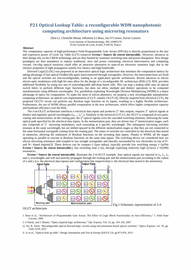
P21 Optical Lookup Table: a reconfigurable WDM nanophotonic computing architecture using microring resonators
Zhen Li, Christelle Monat, Sébastien Le Beux, Ian O’Connor, Xavier Letartre Lyon Institute of Nanotechnology, INL-UMR5270 Ecole Centrale de Lyon, Ecully, F-69134, France
Abstract The computation capacity of high-performance Field Programmable Gate Arrays (FPGAs) is directly proportional to the size and expressive power of Look Up Table (LUT) resources Erreur ! Source du renvoi introuvable.. However, advances in their design rely on the CMOS technology and are thus limited by transistor switching time and power dissipation. New design paradigms are thus mandatory to replace traditional, slow and power consuming, electrical interconnects and computing circuits. On-chip optical resources could offer an attractive alternative to state-of-art electronic transistor logic due to the intrinsic properties of light propagation namely low latency and high bandwidth.
Directed Logic[2] (DL) was proposed as an innovative optical logic architecture that minimize the computation latency by taking advantage of fast optical Fredkin-like gates interconnected through waveguides. However, the interconnections are fixed and the optical switches are non-reconfigurable, leading to an application specific architecture. Recent advances in silicon electro-optic modulators with high bit rates allow for the design of a reconfigurable DL architecture (RDL) [3]. RDL provides additional flexibility by using two sets of (re)configurable add-drop based cells. This can map a lookup table onto an optical switch fabric to perform different logic functions, but does not allow multiple and distinct operations to be computed simultaneously using different wavelengths. Yet, parallelism exploiting Wavelength Division Multiplexing (WDM) is a major advantage of optics for computation. To make the most of silicon photonics, we propose a new reconfigurable nanophotonic computing architecture: an optical core implementation of LUT, namely OLUT [4]. Directly inspired from electrical LUTs, the proposed OLUTs circuit can perform any Boolean logic function on its inputs, resulting in a highly flexible architecture. Furthermore, the use of WDM allows parallel computation in the new architecture, which offers higher computation capacity and hardware efficiency over the RDL.
The n-m-OLUT architecture interfaces n electrical data inputs and produces 2n data outputs, requires 2n optical signals at distinct and regularly spaced wavelengths (λ0,..., λ2
n-1). Similarly to the electrical LUT [1], the OLUT is composed of two parts:
routing and memorization. In the routing part, the 2n optical signals cross the cascaded switching elements, following the same optical path specified by the electrical data inputs. In the memorization part, they are driven into 2n memorization stages, each one composed of 2n microring modulators, each resonating at a specific wavelength. The subsequent microring switches resonate at the same wavelength, but are shifted upward in the different memorization stages so that they are not connected to the same horizontal waveguide coming from the routing part. The states of switches are controlled by the electrical data stored in memories, allowing the realization of Boolean functions on the incoming data inputs. Thanks to WDM, all the stages operating in parallel to execute m Boolean functions on the same data inputs. The switching device we considered here are silicon microring resonators side-coupled to two straight waveguides and laterally surrounded by two electrodes on top of P+ and N+ doped regions[3]. These devices can be compact (~2µm radius), typically provide low switching energy (~1pJ/bit Erreur ! Source du renvoi introuvable.), fast switching time (~ns), through exploiting relatively high Q-factor (~10,000) resonances.
Erreur ! Source du renvoi introuvable. illustrates the 2-4-OLUT example: four optical signals are injected at λ0, λ1, λ2 and λ3 wavelengths and will successively propagate through the routing part and the memorization part according to the values of x and y (i.e. the electrical data inputs) and configuration bits respectively(i.e. the electrical data stored in the memories).
Fig.1 Schematic representation of 2-4-OLUT architecture
J. Rose et al., “Architecture of Programmable Gate Arrays: The Effect of Logic Block Functionality on Area Efficiency,” J. Solid State
Circuits, 1990 J. G Hardy, and J. Shamir, “Optics inspired logic architecture,” Opt. Express, Vol. 15, pp. 150–165, 2007 Q. Xu, R. Soref, “Reconfigurable optical directed-logic circuits using microresonator-based optical switches,” Optics Express, vol. 19, pp.
5244–5259, 2011 Z. Li et al., “Optical look up table”, Design Automation and Test in Europe (DATA’13), pp 873-876, 2013
yx
0/1
z0
Routing part Memorization part
z1
λ0
λ0
λ0
λ0
0/1
0/1
0/1
0/1
0/1
0/1
0/1
0/1
z2 z3
λ2
λ2
λ2
λ2
0/1
0/1
0/1
0/1
0/1
0/1
0/1 λ3
λ3
λ3
λ3
λ1
λ1
λ1
λ1
λx
λx
λx
}λ0λ1λ2λ3
D D D D
Input Data Output Datayx
0/1
z0
Routing part Memorization part
z1
λ0
λ0
λ0
λ0
0/1
0/1
0/1
0/1
0/1
0/1
0/1
0/1
z2 z3
λ2
λ2
λ2
λ2
0/1
0/1
0/1
0/1
0/1
0/1
0/1 λ3
λ3
λ3
λ3
λ1
λ1
λ1
λ1
λx
λx
λx
}λ0λ1λ2λ3
λ0λ1λ2λ3
D D D D
Input Data Output Data
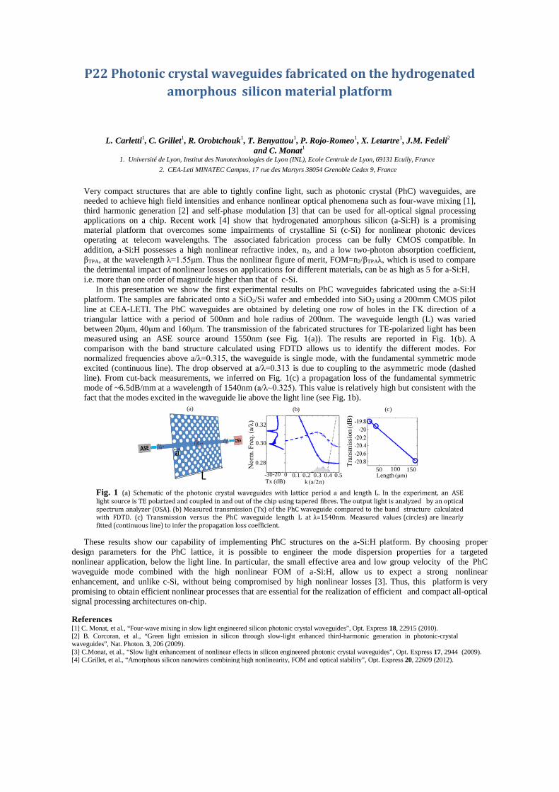
P22 Photonic crystal waveguides fabricated on the hydrogenated amorphous silicon material platform
L. Carletti1, C. Grillet1, R. Orobtchouk1, T. Benyattou1, P. Rojo-Romeo1, X. Letartre1, J.M. Fedeli2
and C. Monat1
1. Université de Lyon, Institut des Nanotechnologies de Lyon (INL), Ecole Centrale de Lyon, 69131 Ecully, France 2. CEA-Leti MINATEC Campus, 17 rue des Martyrs 38054 Grenoble Cedex 9, France
Very compact structures that are able to tightly confine light, such as photonic crystal (PhC) waveguides, are needed to achieve high field intensities and enhance nonlinear optical phenomena such as four-wave mixing [1], third harmonic generation [2] and self-phase modulation [3] that can be used for all-optical signal processing applications on a chip. Recent work [4] show that hydrogenated amorphous silicon (a-Si:H) is a promising material platform that overcomes some impairments of crystalline Si (c-Si) for nonlinear photonic devices operating at telecom wavelengths. The associated fabrication process can be fully CMOS compatible. In addition, a-Si:H possesses a high nonlinear refractive index, n2, and a low two-photon absorption coefficient, βTPA, at the wavelength λ=1.55μm. Thus the nonlinear figure of merit, FOM=n2/βTPAλ, which is used to compare the detrimental impact of nonlinear losses on applications for different materials, can be as high as 5 for a-Si:H, i.e. more than one order of magnitude higher than that of c-Si.
In this presentation we show the first experimental results on PhC waveguides fabricated using the a-Si:H platform. The samples are fabricated onto a SiO2/Si wafer and embedded into SiO2 using a 200mm CMOS pilot line at CEA-LETI. The PhC waveguides are obtained by deleting one row of holes in the ΓK direction of a triangular lattice with a period of 500nm and hole radius of 200nm. The waveguide length (L) was varied between 20μm, 40μm and 160μm. The transmission of the fabricated structures for TE-polarized light has been measured using an ASE source around 1550nm (see Fig. 1(a)). The results are reported in Fig. 1(b). A comparison with the band structure calculated using FDTD allows us to identify the different modes. For normalized frequencies above a/λ=0.315, the waveguide is single mode, with the fundamental symmetric mode excited (continuous line). The drop observed at a/λ=0.313 is due to coupling to the asymmetric mode (dashed line). From cut-back measurements, we inferred on Fig. 1(c) a propagation loss of the fundamental symmetric mode of ~6.5dB/mm at a wavelength of 1540nm (a/λ~0.325). This value is relatively high but consistent with the fact that the modes excited in the waveguide lie above the light line (see Fig. 1b).
(a) (b) (c)
0.32
0.30
a 0.28
L -30-20 0
0.1 0.2 0.3 0.4 0.5
50 100 150 Length (μm)
Tx (dB) k (a/2π)
Fig. 1 (a) Schematic of the photonic crystal waveguides with lattice period a and length L. In the experiment, an ASE light source is TE polarized and coupled in and out of the chip using tapered fibres. The output light is analyzed by an optical spectrum analyzer (OSA). (b) Measured transmission (Tx) of the PhC waveguide compared to the band structure calculated with FDTD. (c) Transmission versus the PhC waveguide length L at λ=1540nm. Measured values (circles) are linearly fitted (continuous line) to infer the propagation loss coefficient.
These results show our capability of implementing PhC structures on the a-Si:H platform. By choosing proper
design parameters for the PhC lattice, it is possible to engineer the mode dispersion properties for a targeted nonlinear application, below the light line. In particular, the small effective area and low group velocity of the PhC waveguide mode combined with the high nonlinear FOM of a-Si:H, allow us to expect a strong nonlinear enhancement, and unlike c-Si, without being compromised by high nonlinear losses [3]. Thus, this platform is very promising to obtain efficient nonlinear processes that are essential for the realization of efficient and compact all-optical signal processing architectures on-chip.
References [1] C. Monat, et al., “Four-wave mixing in slow light engineered silicon photonic crystal waveguides”, Opt. Express 18, 22915 (2010). [2] B. Corcoran, et al., “Green light emission in silicon through slow-light enhanced third-harmonic generation in photonic-crystal waveguides”, Nat. Photon. 3, 206 (2009). [3] C.Monat, et al., “Slow light enhancement of nonlinear effects in silicon engineered photonic crystal waveguides”, Opt. Express 17, 2944 (2009). [4] C.Grillet, et al., “Amorphous silicon nanowires combining high nonlinearity, FOM and optical stability”, Opt. Express 20, 22609 (2012).
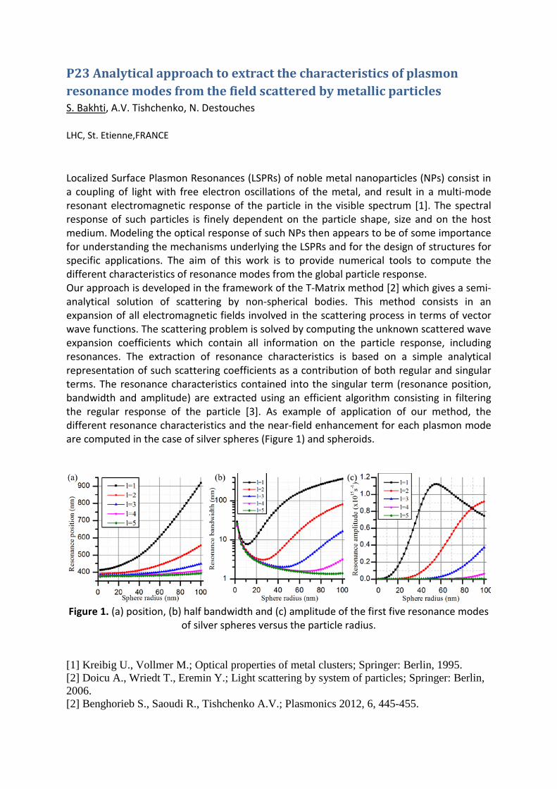
P23 Analytical approach to extract the characteristics of plasmon resonance modes from the field scattered by metallic particles S. Bakhti, A.V. Tishchenko, N. Destouches LHC, St. Etienne,FRANCE Localized Surface Plasmon Resonances (LSPRs) of noble metal nanoparticles (NPs) consist in a coupling of light with free electron oscillations of the metal, and result in a multi-mode resonant electromagnetic response of the particle in the visible spectrum [1]. The spectral response of such particles is finely dependent on the particle shape, size and on the host medium. Modeling the optical response of such NPs then appears to be of some importance for understanding the mechanisms underlying the LSPRs and for the design of structures for specific applications. The aim of this work is to provide numerical tools to compute the different characteristics of resonance modes from the global particle response. Our approach is developed in the framework of the T-Matrix method [2] which gives a semi-analytical solution of scattering by non-spherical bodies. This method consists in an expansion of all electromagnetic fields involved in the scattering process in terms of vector wave functions. The scattering problem is solved by computing the unknown scattered wave expansion coefficients which contain all information on the particle response, including resonances. The extraction of resonance characteristics is based on a simple analytical representation of such scattering coefficients as a contribution of both regular and singular terms. The resonance characteristics contained into the singular term (resonance position, bandwidth and amplitude) are extracted using an efficient algorithm consisting in filtering the regular response of the particle [3]. As example of application of our method, the different resonance characteristics and the near-field enhancement for each plasmon mode are computed in the case of silver spheres (Figure 1) and spheroids.
Figure 1. (a) position, (b) half bandwidth and (c) amplitude of the first five resonance modes
of silver spheres versus the particle radius. [1] Kreibig U., Vollmer M.; Optical properties of metal clusters; Springer: Berlin, 1995. [2] Doicu A., Wriedt T., Eremin Y.; Light scattering by system of particles; Springer: Berlin, 2006. [2] Benghorieb S., Saoudi R., Tishchenko A.V.; Plasmonics 2012, 6, 445-455.

P 24 Transformation Optics with Cylindrical Symmetry and Lossy Media: An Analytical Approach
Mariana Dalarsson,a Martin Norgrena and Zoran Jakšićb a Division of Electromagnetic Engineering, School of Electrical Engineering,
Royal Institute of Technology, SE-100 44 Stockholm, Sweden [email protected] , [email protected]
b Centre of Microelectronic Technologies, Institute of Chemistry, Technology and Metallurgy, University of Belgrade, Njegoševa 12, 11000 Belgrade, Serbia
[email protected] The advent of metamaterial has enabled the emergence of transformation optics with numerous proposed applications that include cloaking devices, superconcentrators, superabsorbers, beam shapers and benders, field and polarization rotators, etc. [1]. The possibility to use metamaterials with tailorable frequency dispersion and with optical properties that can have a custom designed spatial dependence (gradient index metamaterials) [2] has ensured a vast degree of freedom in designing transformation optics. The cylindrical geometry has been one of the prototypal proposed forms, its simplicity being one of the reasons why the first theoretical and experimental cloaking devices had radial symmetry [3], [4]. In this contribution we present an exact analytical approach to solution of Helmholtz’ equations [5] applied to radial propagation of electromagnetic waves through a cylinder containing negative and positive refractive index parts that are linearly graded (Fig. 1 left). Our approach is inspired by the correspondence between transformation optics and quantum mechanics [6]. A remarkably simple analytical solution that does not utilize Bessel functions (Fig. 1 right) is derived.
Fig. 1. Left: Cylindrical geometry incorporating negative and positive index parts with linearly graded refractive index; right: magnetic field intensity versus radial distance
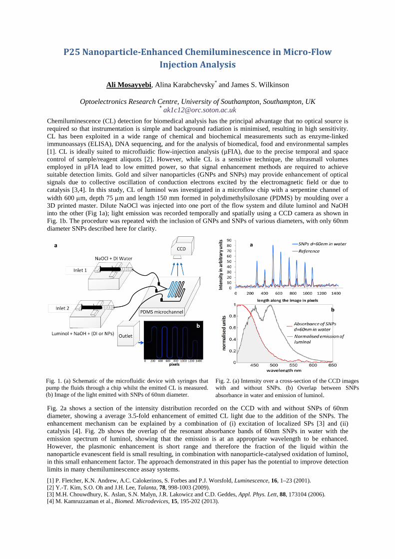
P25 Nanoparticle-Enhanced Chemiluminescence in Micro-Flow Injection Analysis
Ali Mosayyebi, Alina Karabchevsky* and James S. Wilkinson
Optoelectronics Research Centre, University of Southampton, Southampton, UK
Chemiluminescence (CL) detection for biomedical analysis has the principal advantage that no optical source is required so that instrumentation is simple and background radiation is minimised, resulting in high sensitivity. CL has been exploited in a wide range of chemical and biochemical measurements such as enzyme-linked immunoassays (ELISA), DNA sequencing, and for the analysis of biomedical, food and environmental samples [1]. CL is ideally suited to microfluidic flow-injection analysis (µFIA), due to the precise temporal and space control of sample/reagent aliquots [2]. However, while CL is a sensitive technique, the ultrasmall volumes employed in µFIA lead to low emitted power, so that signal enhancement methods are required to achieve suitable detection limits. Gold and silver nanoparticles (GNPs and SNPs) may provide enhancement of optical signals due to collective oscillation of conduction electrons excited by the electromagnetic field or due to catalysis [3,4]. In this study, CL of luminol was investigated in a microflow chip with a serpentine channel of width 600 µm, depth 75 µm and length 150 mm formed in polydimethylsiloxane (PDMS) by moulding over a 3D printed master. Dilute NaOCl was injected into one port of the flow system and dilute luminol and NaOH into the other (Fig 1a); light emission was recorded temporally and spatially using a CCD camera as shown in Fig. 1b. The procedure was repeated with the inclusion of GNPs and SNPs of various diameters, with only 60nm diameter SNPs described here for clarity.
Fig. 1. (a) Schematic of the microfluidic device with syringes that pump the fluids through a chip whilst the emitted CL is measured. (b) Image of the light emitted with SNPs of 60nm diameter.
Fig. 2. (a) Intensity over a cross-section of the CCD images with and without SNPs. (b) Overlap between SNPs absorbance in water and emission of luminol.
Fig. 2a shows a section of the intensity distribution recorded on the CCD with and without SNPs of 60nm diameter, showing a average 3.5-fold enhancement of emitted CL light due to the addition of the SNPs. The enhancement mechanism can be explained by a combination of (i) excitation of localized SPs [3] and (ii) catalysis [4]. Fig. 2b shows the overlap of the resonant absorbance bands of 60nm SNPs in water with the emission spectrum of luminol, showing that the emission is at an appropriate wavelength to be enhanced. However, the plasmonic enhancement is short range and therefore the fraction of the liquid within the nanoparticle evanescent field is small resulting, in combination with nanoparticle-catalysed oxidation of luminol, in this small enhancement factor. The approach demonstrated in this paper has the potential to improve detection limits in many chemiluminescence assay systems.
[1] P. Fletcher, K.N. Andrew, A.C. Calokerinos, S. Forbes and P.J. Worsfold, Luminescence, 16, 1–23 (2001). [2] Y.-T. Kim, S.O. Oh and J.H. Lee, Talanta, 78, 998-1003 (2009). [3] M.H. Chouwdhury, K. Aslan, S.N. Malyn, J.R. Lakowicz and C.D. Geddes, Appl. Phys. Lett, 88, 173104 (2006). [4] M. Kamruzzaman et al., Biomed. Microdevices, 15, 195-202 (2013).
P26 From a plasmonic vortex to a singular beam
Y. Gorodetski, A. Drezet, C. Genet, and T. W. Ebbesen
ISIS, Université de Strasbourg and CNRS (UMR 7006),
8 allée Gaspard Monge, 67000 Strasbourg, France
[email protected] Structured light beams with phase or polarization singularities, and their interaction with
chiral structures has recently become an important research topic1. Nature provides us with state-of-art nanofabricated chiral structures, such as the ones found for instance on Scarab beetles, which are known to modulate the reflected light’s polarization2. Recently, incident polarization handedness was shown to induce chiral surface plasmon (SP) modes – plasmonic vortices – which have been shown to carry orbital angular momentum (OAM)3,4. While the coupling of incident circularly polarized light to the near-field OAM is widely discussed1, 3, 4, studies on the OAM beaming are scarce5.
Here we explore the ability to induce and modify the far-field OAM through managing chiral plasmonic fields6. The experiments were performed using spiral plasmonic structures fabricated on both sides of a suspended 300 nm-thick metal film. Both sides were connected by a subwavelength cylindrical hole located in the center of the plasmonic spirals and perforated through the film. The structure on the input side provides the in-coupling conversion of the incident polarization to a near-field OAM. The excited SP mode is being transmitted to the back side through the hole and decoupled to the far-field by the second structure while acquiring an additional OAM. The hole plays an essential role in the transmission process as it modifies the transmitted OAM through the angular momentum cut-off conditions. A theoretical model, describing the in-coupling, hole transmission and out-coupling processes was developed and verified by experiment.
References
[1] N. M. Litchinitser, Science, 337, 1054 (2012). [2] A. A. Michelson, On Metallic Colouring in Birds and Insects, Phil. Mag. 21, 554-567
(1911). [3] Y. Gorodetski, A. Niv, V. Kleiner, and E. Hasman, Phys. Rev. Lett. 101, 043903
(2008). [4] V. E. Lembessis, S. Al-Aw, M. Babiker, and D. L. Andrews, J. Opt. 13, 64002
(2011). [5] G. Rui, R. L. Nelson, and Q. Zhan Opt. Lett. 20, 18819 (2012). [6] Y. Gorodetski, C. Genet, A. Drezet, and T. W. Ebbesen, Phys. Rev. Lett. 110, 203906
(2013).

P27 Photonic/Plasmonic coupling: A way towards higher performance sensors
Huanhuan Liu1, Mohsen Erouel1, Emmanuel Gerelli2, Abdelmounaim Harouri2, Taha Benyattou2, Régis Orobtchouk2, Laurent Milord2, Ali Belarouci1, Xavier Letartre1, Cécile
Jamois2
1 Université de Lyon; Institut des Nanotechnologies de Lyon INL - CNRS UMR5270, Ecole Centrale de Lyon, Ecully, F-69134, France
2 Université de Lyon; Institut des Nanotechnologies de Lyon INL - CNRS UMR5270, INSA de Lyon,
Villeurbanne, F-69621, France [email protected]
The increasing concern for environmental analysis and food quality control as well as the need for medicine monitoring leads to a growing need for new kinds of chemical and biological sensors with highly sensitive and specific detection of molecules. Among the wide diversity of available sensors, optical sensors are of high interest, as they allow label-free and specific detection of a large variety of molecules [1, 2]. In this paper, we propose a new kind of optical sensor with enhanced sensitivity, which is based on the coupling between a photonic dielectric device and plasmonic nanoantennas (NAs). The photonic device consists of a porous silicon interferometer realized via anodization. The array of bowtie nanoantennas is fabricated using standard processes like electron beam lithography and lift-off. The coupling mechanisms occurring within the hybrid structure are studied with an interferometer approach, where the NA array is supposed to be equivalent to a homogeneous layer with the same specific dielectric function placed on top of the interferometer. Based on the phase matching condition of thin-film interferometer, the fringe variations induced by the introduction of the equivalent layer can be analyzed. We will show that the optical response of the hybrid structure exhibits both the enhancement of NA resonance and the fringe pattern of the interferometer, with some additional features: a splitting of the interferometer fringes occurs at NA resonance, indicating strong coupling between the NAs and the interferometer [3]. The resulting sensitivity to variations of refractive index in the device environment is much larger, highlighting the potential for sensing applications.
Illustration of hybrid device based on porous silicon interferometer and bowtie NAs.
[1] C. Jamois, C. Li, E. Gerelli, Y. Chevolot, V. Monnier, R. Skrshevskyi, R. Orobtchouk, E. Souteyrand, and T. Benyattou, “Porous-Silicon Based Planar Photonic Crystals For Sensing Applications”, SPIE, vol. 1, pp 7713-7729, 2010 [2] X.D. Fan, I. M. White, S. I. Shopova, H.Y. Zhu, J. D. Suter, and Y.Z. Sun, “Sensitive Optical Biosensors for Unlabeled Targets: A Review ”, Analytica Chimica Acta, vol. 6 2 0, pp.8-26, 2008 [3] Ameling, Ralf, and Harald Giessen. "Cavity plasmonics: large normal mode splitting of electric and magnetic particle plasmons induced by a photonic microcavity.", Nano letters 10, no. 11 (2010): 4394-4398.
P28 Photon Cages R. Artinyan1, A. Benamrouche, C. Belacel, A. Berthelot, A.M. Jurdyc, P. Rojo-Romeo, G.
Grenet, A. Danescu, P. Regreny, J.L. Leclercq, X. Letartre, S. Callard 1email : [email protected]
We suggest new microphotonic structures for the 3D-confinement of light in low index materials [1],[2]. This kind of confinement is especially useful for sensing applications. Because of their scale and geometry, developing optical characterization techniques for these hollow cavities is one of the challenges we are facing. We have used FDTD simulations to predict the behaviour of the optical modes of photon cages under a variety of stimuli, and have accordingly built both far field and near field optical characterization setups to tackle this issue. The fabrication of photon cages containing active light emitters has also been considered to help characterize the cages. We therefore had to redesign the structures to take the modified optical index of the emitter-containing media into account. We present the concept of these hollow cavities, their designing process and the results of our first characterization attempts. References [1] C. Sieutat, R. Peretti, J. L. Leclercq, P. Viktorovitch, and X. Letartre : Strong confinement of light in low index materials: the Photon Cage, Optics Express no20015, 2013. [2] A. Danescu, C. Chevalier, G. Grenet, Ph. Regreny, X. Letartre, and J. L. Leclercq : Spherical curves design for micro-origami using intrinsic stress relaxation, Applied Physics Letters 102, 123111, 2013 Acknowledgements We thank R.Peretti, L.Lalouat and B.Gonzalez-Acevedo for their help and advice regarding FDTD computing. We acknowledge iMust and Région Rhône-Alpes for the funding of this research.