MEASURING LEVEL OF DEGRADATION IN POWER …
171
MEASURING LEVEL OF DEGRADATION IN POWER SEMICONDUCTOR DEVICES USING EMERGING TECHNIQUES A DISSERTATION IN Electrical and Computer Engineering & Mathematics Presented to the Faculty of the University of Missouri-Kansas City in partial fulfillment of the requirements for the degree DOCTOR OF PHILOSOPHY by ABU HANIF B.S., Electrical and Electronic Engineering Bangladesh University of Engineering and Technology, 2013 Kansas City, Missouri 2021
Transcript of MEASURING LEVEL OF DEGRADATION IN POWER …

i
MEASURING LEVEL OF DEGRADATION IN POWER SEMICONDUCTOR
DEVICES USING EMERGING TECHNIQUES
A DISSERTATION IN
Electrical and Computer Engineering
&
Mathematics
Presented to the Faculty of the University of
Missouri-Kansas City in partial fulfillment of
the requirements for the degree
DOCTOR OF PHILOSOPHY
by
ABU HANIF
B.S., Electrical and Electronic Engineering
Bangladesh University of Engineering and Technology, 2013
Kansas City, Missouri
2021

ii
© 2021
ABU HANIF
ALL RIGHTS RESERVED

iii
MEASURING LEVEL OF DEGRADATION IN POWER SEMICONDUCTOR
DEVICES USING EMERGING TECHNIQUES
Abu Hanif, Candidate for Doctor of Philosophy Degree
University of Missouri-Kansas City, 2021
ABSTRACT
High thermal and electrical stress, over a period of time tends to deteriorate the health
of power electronic switches. Being a key element in any high-power converter systems, power
switches such as insulated-gate bipolar junction transistors (IGBTs) and metal-oxide
semiconductor field-effect transistors (MOSFETs) are constantly monitored to predict when
and how they might fail. A huge fraction of research efforts involves the study of power
electronic device reliability and development of novel techniques with higher accuracy in
health estimation of such devices. Until today, no other existing techniques can determine the
number of lifted bond wires and their locations in a live IGBT module, although this
information is extremely helpful to understand the overall state of health (SOH) of an IGBT
power module. Through this research work, two emerging methods for online condition
monitoring of power IGBTs and MOSFETs have been proposed. First method is based on
reflectometry, more specifically, spread spectrum time domain reflectometry (SSTDR) and
second method is based on ultrasound based non-destructive evaluation (NDE). Unlike
traditional methods, the proposed methods do not require measuring any electrical parameters
(such as voltage or current), therefore, minimizes the measurement error. In addition, both of
these methods are independent of the operating points of the converter which makes the

iv
application of these methods more feasible for any field application. As part of the research,
the RL-equivalent circuit to represent the bond wires of an IGBT module has been developed
for the device under test. In addition, an analytical model of ultrasound interaction with the
bond wires has been derived in order to efficiently detect the bond wire lift offs within the
IGBT power module. Both of these methods are equally applicable to the wide band gap
(WBG) power devices and power converters. The successful implementation of these methods
creates a provision for condition monitoring (CM) hardware embedded gate driver module
which will significantly reduce the overall health monitoring cost.

v
APPROVAL PAGE
The faculty listed below, appointed by the Dean of the School of Graduate Studies,
have examined a thesis titled “Measuring Level of Degradation in Power Semiconductor
Devices using Emerging Techniques” presented by Abu Hanif, candidate for the Doctor of
Philosophy degree, and certify that in their opinion it is worthy of acceptance.
Supervisory Committee
Faisal Khan, Ph.D., Committee Chair
Department of Computer Science and Electrical Engineering
Majid Bani-Yaghoub, Ph.D., Co-discipline Advisor
Department of Mathematics
Ghulam M. Chaudhry, Ph.D.
Department of Computer Science and Electrical Engineering
Masud H. Chowdhury, Ph.D.
Department of Computer Science and Electrical Engineering
Anthony Caruso, Ph.D.
Department of Physics and Astronomy
Mohammed K. Alam, Ph.D.
General Motors

vi
TABLE OF CONTENTS
ABSTRACT ..........................................................................................................................................................iii
LIST OF TABLES ................................................................................................................................................ ix
LIST OF ILLUSTRATIONS.................................................................................................................................. x
ACKNOWLEDGEMENTS ................................................................................................................................xiii
CHAPTER 1 ........................................................................................................................................................... 1
INTRODUCTION .................................................................................................................................................. 1
1.1 Dissertation Outline ..................................................................................................................................... 6
CHAPTER 2 ........................................................................................................................................................... 7
FAILURE MECHANISMS OF MODERN POWER ELECTRONIC DEVICES ................................................. 7
2.1 Introduction ................................................................................................................................................. 7
2.2 Failure Mechanisms ..................................................................................................................................... 7
2.2.1 Chip-related failure mechanisms .......................................................................................................... 8
2.2.2 Package-related failure mechanisms .................................................................................................. 10
2.3 Conclusions ............................................................................................................................................... 12
CHAPTER 3 ......................................................................................................................................................... 13
EXISTING DEGRADATION DETECTION & LIFETIME PREDICTION TECHNIQUES ............................. 13
3.1 Introduction ............................................................................................................................................... 13
3.2 Failure mechanism-based lifetime prediction ............................................................................................ 15
3.2.1 Bond wire failure models ................................................................................................................... 15
3.2.2 Solder fatigue models......................................................................................................................... 20
3.2.3 Real-time lifetime estimation ............................................................................................................. 23
3.3 Failure precursor-based lifetime prediction ............................................................................................... 25
3.3.1 Failure precursors of power electronics devices ................................................................................ 25
3.3.2 Precursor parameter measurements .................................................................................................... 26
3.3.3 Remaining useful life prediction ........................................................................................................ 28
3.4 Conclusions ............................................................................................................................................... 29

vii
CHAPTER 4 ......................................................................................................................................................... 31
ACCELERATED AGING METHODS ............................................................................................................... 31
4.1 Introduction ............................................................................................................................................... 31
4.2 Device qualification tests ........................................................................................................................... 31
4.3 Test for exploring failure mechanisms or failure precursors ................................................................... 32
4.4 Tests to verify condition monitoring methods ........................................................................................... 35
4.5 Tests considering mission profiles ............................................................................................................. 36
4.6 Conclusions ............................................................................................................................................... 45
CHAPTER 5 ......................................................................................................................................................... 47
SSTDR BASED DEGRADATION DETECTION .............................................................................................. 47
5.1 Introduction ............................................................................................................................................... 47
5.2 Fundamentals of SSTDR ........................................................................................................................... 48
5.3 Accelerated Aging and Degradation Detection ......................................................................................... 51
5.3.1 Active Power Cycling of IGBT .......................................................................................................... 51
5.3.2 Experimental Setup and Test Results ................................................................................................. 54
5.4 RL-Equivalent of the Bond Wires in IGBT Module .................................................................................. 60
5.4.1 Simulation Results ............................................................................................................................. 64
5.4.2 Simulation vs Experimental Results .................................................................................................. 68
5.5 Conclusions ............................................................................................................................................... 70
CHAPTER 6 ......................................................................................................................................................... 72
ULTRASOUND BASED DEGRADATION DETECTION ................................................................................ 72
6.1 Introduction ............................................................................................................................................... 72
6.2 Ultrasound Fundamentals and Sympathetic String Theory ....................................................................... 73
6.2.1 Ultrasound resonator – a new way of testing electronics live ............................................................ 73
6.2.2 Sympathetic resonance in acoustic string instrument ......................................................................... 76
6.3 Analytical Model of Ultrasound Wave Propagation in IGBT Module ...................................................... 79
6.3.1 Modes of sound wave propagation: ................................................................................................... 79
6.3.2 Frequency, wavelength, and defect detection: ................................................................................... 82

viii
6.3.3 Attenuation of ultrasound wave ......................................................................................................... 84
6.3.4 Snell’s Law, wave equation, and reflection amplitudes ..................................................................... 85
6.4 Experimental Setup and Results ................................................................................................................ 90
6.5 Conclusions ............................................................................................................................................... 95
CHAPTER 7 ......................................................................................................................................................... 97
DEGRADATION DETECTION OF WIDE BANDGAP POWER DEVICES ................................................... 97
7.1 Introduction ............................................................................................................................................... 97
7.2 Aging in MOSFETs: Equivalent Impedance Approach ............................................................................. 99
7.2.1 Origin of Aging .................................................................................................................................. 99
7.2.2 Gate-Source Impedance: An Aging Precursor ................................................................................. 100
7.3 Case Study-1: Degradation Detection in a Discrete SiC MOSFET ......................................................... 101
7.3.1 Standardized Accelerated Aging Methodology ............................................................................... 102
7.3.2 SSTDR Test Setup ........................................................................................................................... 103
7.3.3 Test Results ...................................................................................................................................... 104
7.4 Case Study-2: Degradation detection in a SiC based buck converter ...................................................... 106
7.4.1 Aging in Buck Converter ................................................................................................................. 107
7.4.2 Experimental Setup .......................................................................................................................... 108
7.4.3 Test Results ...................................................................................................................................... 110
7.5 Case Study-3: Degradation Detection of Thermally Aged Si and SiC Power MOSFET......................... 112
7.5.1 Experimental Setup .......................................................................................................................... 113
7.5.2 Test Results ...................................................................................................................................... 116
7.6 Conclusions ............................................................................................................................................. 119
CHAPTER 8 ....................................................................................................................................................... 122
CONCLUSIONS AND FUTURE RESEARCH ................................................................................................ 122
REFERENCES ................................................................................................................................................... 124
VITA .................................................................................................................................................................. 155
ix
LIST OF TABLES
Table I Comparison between Failure Mechanisms [66] ............................................................................. 12
Table II Comparison between Failure Methods [68] .................................................................................. 14
Table III Comparison between Lifetime Prediction Methods ..................................................................... 29
Table IV Standard Tests for the Qualification of SKIM Modules [125]..................................................... 32
Table V RAPSDRA Test Protocols [129] ................................................................................................... 33
Table VI Comparison of Temperature Measurement Methods .................................................................. 45
Table VII Correlation between VCEON And SSTDR Amplitude .................................................................. 57
Table VIII Parametric Values of the Elements in RL-Equivalent Circuit of the IGBT Module ................. 63
Table IX Simulation Phases ........................................................................................................................ 64
Table X Actual Data Points for both Scenarios .......................................................................................... 67
Table XI Acoustic Behavior of the Gel Layer inside FR450R12ME4 Dual Pack IGBT Module ............... 79
Table XII Comparison between RDSON and SSTDR Amplitude ............................................................... 119

x
LIST OF ILLUSTRATIONS
Figure 1: Survey of Different Components Responsible for Converter Failure [20] .................................... 3
Figure 2: Failure Mechanisms of Power Electronic Devices ........................................................................ 8
Figure 3: Typical Multilayer Structure of a Power Module ........................................................................ 10
Figure 4: Number of Cycles Vs. Temperature Swing [69] ......................................................................... 17
Figure 5: Number of Cycles Vs. Crack Length. .......................................................................................... 22
Figure 6: RC Thermal Models (A) Cauer (B) Foster [133-135] ................................................................. 43
Figure 7: Schematic Diagram of the SSTDR System Showing the Setup to Characterize an IGBT in a
Live Converter. [Courtesy: Livewire Innovation, 2012] [19] ..................................................................... 48
Figure 8: Photograph of the FPGA-Based SSTDR Hardware (an R&D Product from Livewire
Innovation). ................................................................................................................................................. 49
Figure 9: (A) Infineon Dual Pack IGBT Module (FF450R12ME4) without Top Cover (B) Simplified
Schematic of the Module ............................................................................................................................ 50
Figure 10: Infineon IGBT Power Module (FF450R12ME4) without Top Cover ....................................... 52
Figure 11: Active Power Cycling Setup ...................................................................................................... 53
Figure 12: Schematic of the Accelerated Aging Station ............................................................................. 54
Figure 13: VCEON Vs. Number of Cycles Plot ............................................................................................. 55
Figure 14: Simplified SSTDR Test Schematic: TP1 and TP2 Represent SSTDR Test Points for Top and
Bottom IGBT’s Gate-Emitter Interface Respectively ................................................................................. 56
Figure 15: SSTDR Auto-Correlated Amplitude Plot .................................................................................. 56
Figure 16: SSTDR Auto-Correlated Amplitude Plot .................................................................................. 58
Figure 17: SSTDR Auto-Correlated Amplitude Plot .................................................................................. 59
Figure 18: Simplified Block Diagram Of FF450R12ME4 Dual Pack IGBT Power Module...................... 60
Figure 19: (A) RL-Equivalent of a Single Pair of IGBT and Diode (B) Simplified Schematic of a Single
Pair of IGBT and Diode .............................................................................................................................. 61
Figure 20: Finalized Bond Wire RL-Equivalent Circuit of the IGBT Module ........................................... 63
Figure 21: Reflection Magnitude Vs. Frequency Plot when T2 has Lifted Bond Wire (A) Recorded at G1-
E1 Interface (B) Recorded at G2-E2 Interface .............................................................................................. 65
Figure 22: Reflection Magnitude Vs. Frequency Plot when B2 has Lifted Bond Wire (A) Recorded at G1-
E1 Interface (B) Recorded at G2-E2 Interface .............................................................................................. 65
Figure 23: Peak Reflection Amplitude Plot for Six Device Locations (A) Recorded at G1-E1 Interface (B)
Recorded at G2-E2 Interface ........................................................................................................................ 66
xi
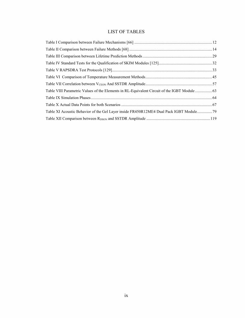
Figure 24: (A) The Actual Test Setup (B) Photograph of the Actual IGBT Module used with and without
Top Cover (C) Close-up View of the IGBT Bond Wires. ........................................................................... 69
Figure 25: Simulation and Experimental Results Show the Similar Pattern in the Peak Magnitude with
Equal Number of Bond Wire Lift Off Scenario at 12MHz Frequency (A) Obtained through Simulation
(B) Recorded from Experiments ................................................................................................................. 70
Figure 26: Simulation and Experimental Results Show the Similar Pattern in the Peak Magnitude with
Equal Number of Bond Wire Lift Off Scenario at 48MHz Frequency (A) Obtained through Simulation
(B) Recorded from Experiments ................................................................................................................. 70
Figure 27: Interaction of an Ultrasonic Shear Wave From s Surface Crack ............................................... 76
Figure 28: (A) Sympathetic Strings in an Electric Sitar (Courtesy: Wikimedia), (B) Incident and Reflected
Signal to and from the IGBT Bond Wire, (C) Actual IGBT Bond Wires ................................................... 78
Figure 29: Particle Movement Illustration of Longitudinal and Shear Waves ............................................ 80
Figure 30: Critical Angles for an Incident Ultrasound Wave...................................................................... 81
Figure 31: Ultrasound Wave Interaction at the Interface of Two Media. ................................................... 86
Figure 32: Representation of Physical Distance between Devices and Sensors to Estimate the Attenuated
Ultrasound Signal Received by the Respective Sensors (Not Drawn to Scale). ......................................... 89
Figure 33: Experimental Setup for Ultrasound Resonator-Based Condition Monitoring of IGBT Power
Module: (A) FF450R12ME4 IGBT Dual Pack Module without Top Cover, (B) Bottom View of the
Inserted PCB to Show the Resonators in Prototype 1, (C) Top View with BNC Connectors in Prototype
2 .................................................................................................................................................................. 91
Figure 34: Bond Wire Lift Off and Corresponding Current Crowding (The Red Circle Shows Damaged
Bond Wires). ............................................................................................................................................... 92
Figure 35: Time and Frequency Domain Data from Sensor 1 .................................................................... 93
Figure 36: Time and Frequency Domain Data from Sensor 4 .................................................................... 94
Figure 37: Time and Frequency Domain Data from Sensor 3 .................................................................... 95
Figure 38: Simplified Equivalent Circuit of a SIC Mosfet [183] .............................................................. 100
Figure 39: Accelerated Aging Station. ...................................................................................................... 103
Figure 40: SIC Power Mosfet (C2M0025120D, Manufactured by Cree Inc.) .......................................... 103
Figure 41: Experimental Setup for Degradation Monitoring of DUT. ...................................................... 104
Figure 42: Schematic Diagram of the Experimental Setup for Degradation Monitoring of SIC
MOSFET. .................................................................................................................................................. 104
Figure 43: SSTDR Auto-correlation Plots for New and Aged SIC MOSFETS at Different SSTDR
Frequencies Recorded from the Gate-Source Terminals. ......................................................................... 105
Figure 44: Schematic of a SIC MOSFET based Buck Converter ............................................................. 107
Figure 45: Power Cycling Station ............................................................................................................ 109
Figure 46: Buck Converter Setup to Apply SSTDR ................................................................................ 110
Figure 47: Buck Converter Setup to Apply SSTDR ................................................................................ 110

xii
Figure 48: SSTDR Auto-correlated Amplitude Plots for Healthy and Aged Buck Converter at Different
Frequencies ............................................................................................................................................... 112
Figure 49: DELTA Thermal Aging Chamber ........................................................................................... 114
Figure 50: SSTDR Test Setup ................................................................................................................... 115
Figure 51. Schematic of the SSTDR Experimental Setup for Degradation Monitoring. .......................... 115
Figure 52: Changes in RDSON over Time. .................................................................................................. 116
Figure 53: SSTDR Auto-correlation Plots for New and Aged Si MOSFETS at 48MHz SSTDR
Frequency.................................................................................................................................................. 117
Figure 54: SSTDR Auto-correlation Plots for New and Aged Sic MOSFETS at 48MHz SSTDR
Frequency.................................................................................................................................................. 118
Figure 55: Correlation between RDSON and SSTDR Amplitude ................................................................ 119
xiii
ACKNOWLEDGEMENTS
This work was authored in part by the National Renewable Energy Laboratory (NREL),
operated by Alliance for Sustainable Energy, LLC, for the U.S. Department of Energy (DOE)
under Contract No. DE-AC36-08GO28308. This work was supported by the Laboratory
Directed Research and Development (LDRD) Program at NREL. The views expressed in the
dissertation do not necessarily represent the views of the DOE or the U.S. Government. The
U.S. Government retains and the publisher, by accepting the article for publication,
acknowledges that the U.S. Government retains a nonexclusive, paid-up, irrevocable,
worldwide license to publish or reproduce the published form of this work, or allow others to
do so, for U.S. Government purposes. This research work was partially supported by the
National Science Foundation (NSF) Grant# 1947410 as well.
Foremost, it is a genuine pleasure to express my heartfelt gratitude and appreciation to
my committee chair, mentor, philosopher, and guide, Dr. Faisal Khan, who has the attitude and
the substance of a genius: he continually and convincingly conveyed a spirit of adventure in
regard to research and scholarship, and an excitement in regard to teaching. His dedication and
keen interest to help his students have been vividly noticeable from the very first day I started
working at Missouri Center for Advanced Power (MCAP) laboratory as a graduate research
assistant and lab manager, which had been solely responsible for completing my work. His
timely advice, meticulous scrutiny, scholarly advice, and scientific approach have helped me
significantly to accomplish this task. This dissertation would not have been possible without
his guidance and persistent help. Dr. Khan has been extremely supportive throughout my PhD
journey, especially his compassion during my stressful, struggling, and distressed times are
beyond description. He is a true inspiration for me when it comes to instant problem solving

xiv
skills, ethics, and philosophy. He taught me how to think critically, take ownership of my
projects, improve independent research skills and problem solving ability through our
brainstorming and philosophical meetings. All of these factors along with Dr. Khan’s insightful
feedback and expertise in formulating the research questions and methodologies have pushed
me to sharpen my thinking and improved the quality of research work. I could not have wished
for a smarter and better advisor and mentor for my PhD study. I hope that I can apply the
philosophy and ethics that I have learnt under his supervision in my future career so that the
legacy continues.
After that, I would like to express my sincere gratitude to the rest of my PhD committee
members, Dr. Majid Bani-Yaghoub, Dr. Ghulam M. Chaudhry, Dr. Masud H. Chowdhury, Dr.
Anthony Caruso, and Dr. Mohammed Alam for their advice, support, and guidance throughout
my degree. Their prompt inspirations, timely suggestions, enthusiasm, dynamism have
enabled me to complete this dissertation. Especially, I would like to thank Dr. Caruso for
providing me the opportuning to work with his research group and within the Missouri Institute
of Defense and Energy (MIDE) during the summer of 2016 and 2020, respectively. Both of
these research experiences have helped me to handle and coordinate time-critical projects and
taught to be a team player. Dr. Alam has served as the outside reader in my PhD committee,
and it is my pleasure to express my appreciation for his advice and suggestions in my research
related to the SSTDR based degradation detection.
Then, I would like to thank Patrick O’Bannon, UMKC Staff, for his timely support in
the machine lab during the preparation of ultrasound resonators.
My sincere thanks goes to Douglas DeVoto and Sreekant Narumanchi for offering me
the summer internship opportunity at NREL in their group and leading me working on diverse

xv
exciting projects. I would also like to thank Joshua Major for his technical support and
professional teachings throughout my internship period.
I would also like to thank my fellow lab mates Wasek Azad, Swagat Das, and Sourov
Roy for the fun-times we spent together, the sleepless nights that enabled us to complete tasks
before deadlines, stimulating discussions, and for the happy distractions to rest my mind
outside of my research.
Finally, I am grateful to my parents for bringing me into this world and constantly
keeping me in their prayers for every success in my life. Their countless sacrifices and hardship
can never be described in words. The unconditional love and care they provided me have been
my source of inspiration in every spheres of my life. My wife, Aisha MS Haquie, has endured
most of the pain in taking care of our son Rayan Al Zain and daughter Sarah Al Zain, especially
when I was busy in the lab doing my experiments. Her whole-hearted support and
encouragement have kept me sane throughout my pursuit in achieving this degree. Words are
not enough to express my gratitude to her. The sacrifices she has made for me to make my
research work the highest priority and achieve my milestones in a comparatively smoother way
is beyond anyone’s imagination and nothing can ever do justice to her hard work and sacrifices.
Last but not the least, I thank the Almighty God for the guidance, strength, power of
mind, protection, skills, and for giving us a healthy life. Without any of these, I would not be
able to complete the research works in a timely manner.

xvi
DEDICATION
This dissertation is wholeheartedly dedicated to my beloved parents and my wife, who
continually provide their moral, spiritual, emotional, and financial support. They have been
my source of inspiration and gave me strength whenever I thought of giving up.

1
CHAPTER 1
INTRODUCTION
In recent years, power electronics has penetrated into many industrial applications such
as renewable energy systems, hybrid-electric vehicles, locomotives, space missions, and so on.
One common but major concern in these aforementioned systems is reliability, which is
responsible for economic or safety considerations. As an example, in PV power generation
systems, low reliability will increase maintenance costs and decrease system availability, and
therefore, increase the levelized cost of electricity (LCOE), which will eventually affect its
market penetration. A similar issue exists in offshore wind farms, which is not conveniently or
inexpensively accessible for maintenance. In automobile, locomotive, and avionic
applications, safety requirements impose nearly zero failure tolerance. Many approaches to
address reliability problems of power electronic systems have been proposed and intensively
studied for years. Mainstream efforts include the following: (1) standard-based reliability
assessment [1-5]; (2) fault-tolerant topologies with redundant components [6-8]; (3)
prognostics, health management (PHM), and condition monitoring approaches [9-13]; (4)
designing highly reliable power electronic devices using advanced materials [14-16]. A nice
review covering approaches 1 to 3 is presented in [17]. Among approaches 1 to 4, prognostics
with lifetime estimation functionality is probably the most promising one. Approach 1 is more
suitable in the design stage to get an estimation of overall system reliability. The commonly
used reliability index is the mean time between failures (MTBF) [1]. Although approaches 2
and 4 enhance system reliability, they do not prevent failure from happening. Indeed, failure
is never completely preventable. Therefore, the preferred way is to take action before a failure
occurs, and lifetime prediction, if performed appropriately, can fulfill this mission. If used in

2
the design stage, a lifetime prediction model enables the designer to make proper decisions to
ensure higher reliability. Used in applications, such a model can provide information of any
remaining useful life or level of degradation. Previous studies show that a majority of power
electronic system failures are due to component failures [18]. Therefore, it is a matter of
paramount importance to detect the aging of the power semiconductor devices in order to
estimate the state of health (SOH) of the overall converter circuit. In fact, a lifetime estimation
of power electronic devices is a multi-disciplinary task that requires the cooperation of
electrical engineers, mechanical engineers, and statisticians. We need to identify the failure
precursor parameters as well as understand the dominant failure mechanisms in order to predict
the lifetime of power electronic devices. A proper lifetime prediction method should then be
selected. Finally, the lifetime prediction can be performed.
High-power converters are the key elements in a majority of power electronic
applications. The applications include but are not limited to industrial power systems, FACTs
devices, commercial cooling units, electric vehicles and utility systems, aircrafts, navy and
commercial ships, military applications, and so on [19]. Many of these applications may have
redundancy since they support invaluable systems for homes, transportation, business, and
many more. However, some of the applications e.g., aircrafts may not have the luxury of
redundancy due to the weight limitations and fuel efficiency. Therefore, any application
requiring highly reliable power electronic system needs an accurate estimation of state of
health. The most commonly used power converters are comprised of high power IGBTs and
MOSFETs. These power electronic switches are the most failure prone components in the
entire power converter circuit which was inferred from the industrial survey conducted by the
authors in [20]. The results are shown in Figure 1.

3
In high power applications, IGBTs are manufactured as a module which consists of
more than one IGBT devices. These devices are connected through bond wires (BW) inside a
module. In practical applications, these bond wires experience lift off, surface crack or heel
crack etc., and the device degrades or poorly performs. In order to estimate the level of aging,
electrical parameters such as current, voltage, etc. can be monitored and compared either off-
line with, or in-situ alongside a healthy device. The most commonly used failure precursor
parameters for an IGBT are threshold voltage (Vt), collector-emitter ON-state voltage (VCEON),
collector-emitter current (IC), and case temperature of the semiconductor package (TC) [21-
33]. However, all of these precursor parameter-based condition monitoring techniques are
either highly operating point dependent or extremely hard to perform in a live circuit when the
semiconductor switches are pulsed with PWM signals [34-38]. In order to overcome these
limitations, this research work proposes and institutes two non-invasive and in-situ methods to
identify the degradation in power semiconductor devices/modules.
Figure 1: Survey of different components responsible for converter failure [20]

4
First method is based on spread spectrum time domain reflectometry (SSTDR) which
has opened a new avenue in live condition monitoring, and can be found in many literature
[39-43]. SSTDR based techniques have been successfully carried out in cable fault location in
[39], and aircraft wiring fault location has been identified using SSTDR in [40]. The SSTDR
technique has been effectively utilized to determine PV panel ground fault detection [39], and
PV arc fault detection [42]. However, these existing methods cannot yet identify the location
of the fault and if any bond wire has been detached from the substrate. In addition, these
techniques are unable to detect degradation while the converter or device is live and they
require accessing the high voltage nodes of the converter/inverter circuit.
In contrast, SSTDR based degradation detection has several advantages. First of all, the
signal was applied at the gate-source interface of the module which will eventually make the
measurement technique safer. Secondly, SSTDR frequencies (several MHz) are way above the
converter’s switching frequency, which ensures no interruption in the normal operation of the
power converter. Using this method, any unwanted downtime can be significantly reduced by
performing scheduled maintenance which will eventually provide the converter circuit a longer
life resulting in a reduced overall cost .Through this research, we have overcome the limitations
of the existing methods by applying the SSTDR test signal at the gate-source interface of the
semiconductor device. The proposed method is able to detect aging in both Si and WBG
semiconductor devices as well as the degradation of a converter/inverter circuit. The proposed
method has also been validated by successful detection of the bond wire lift off related aging
in IGBT modules. An RL-equivalent IGBT model of an Infineon dual pack module
(FF450R12ME4) has been established for the first time in order to verify the experimental
result obtained using SSTDR method. This equivalent circuit will help researchers to

5
understand not only the reflectometry based degradation detection but also the other
researchers who will be using this module. In addition, degradation detection of SiC based
power MOSFETs have been studied as well using this novel SSTDR technique.
Second method studies the degradation detection technique for IGBT modules based
on ultrasound. Existing ultrasound based crack or void detection techniques are either too
expensive and/or requires a fluid couplant to submerge the DUT/structure to be tested [44].
Confocal scanning acoustic microscopy (CSAM) based state-of-health identification is very
popular in a semiconductor die and die-attach between the copper layer and substrate [45]-
[47]. However, this technique cannot be used in a live circuit for package level degradation
detection due to the size and medium constraint of the CSAM setup (requires the wafer to be
submerged in water). In addition, it takes a long time to scan the device under test compared
to any other existing condition monitoring method. Electromagnetic acoustic transducers
(EMATs) does not require any couplant, however, they require high current injections for
testing, and their efficiency is not as effective as the piezo-electric transducers [48]. In addition,
the spread spectrum ultrasound technique requires highly precise transducer and couplant
control to generate reasonably reliable results, and this technique has only been applied to large
structures such as steel blocks [49]-[50]. The proposed ultrasound-based technique is able to
detect bond wire lift off related adding in-situ and irrespective of the operating condition of
the module or converter. This proposed method neither require any liquid couplant nor need
measuring any precursor parameter. In addition, this method can be integrated with the gate
driver module if properly scaled. Therefore, it is expected that the successful implementation
of both of the methods will create a seminal impact in estimating remaining life especially for
IGBTs.
6
1.1 Dissertation Outline
This dissertation is organized into eight (8) chapters. Chapter 2 explains the failure
mechanism of the modern power electronic semiconductor devices and includes their
classification. Chapter 3 describes the existing degradation detection and lifetime estimation
methods and their advantages and disadvantages. Chapter 4 details the accelerated aging
methods practiced by the industries and the researchers. SSTDR fundamentals and how this
technique can be utilized in condition monitoring of power switching devices are discussed in
Chapter 5. Chapter 5 also includes the development of an RL-equivalent of the IGBT bond
wires and verifies the model by comparing the simulation and experimental results. Bond wire
lift off related degradation detection of IGBT modules using ultrasound resonators has been
discussed in Chapter 6 as well as the ultrasound propagation inside the IGBT module has been
analytically modeled in this chapter. Chapter 7 includes three (3) case studies where SSTDR
method has been utilized to identify the aging of SiC power MOSFETs as a discrete device as
well as in a live converter circuit. Finally, the conclusions and future work are discussed in
Chapter 8.

7
CHAPTER 2
FAILURE MECHANISMS OF MODERN POWER ELECTRONIC DEVICES
2.1 Introduction
Device degradation is a natural phenomenon. As a result, the semiconductor devices
become vulnerable against the electro-thermal stresses and their durability and performance
greatly downgrade. Therefore, it is an obvious question for the researchers that how these
degradation related failures occur within the semiconductor devices. In other words, the
mechanism behind the failures have been investigated by the scholars and, this chapter
summarizes these failure mechanisms.
2.2 Failure Mechanisms
In general, power electronic devices comprise discrete devices and power electronic
modules. These power electronic devices experience thermal, chemical, electrical, mechanical
stresses, and degrade gradually, leading to a complete failure. Especially for hybrid electric
vehicles (HEVs), the dominant reason of failure arises from thermal stress [51]. It is worth
mentioning that vibration or shock also acts like a catalyst in the degradation process. Previous
studies have grouped failure mechanisms of power electronic devices into two categories,
namely chip-related (or intrinsic) failures and package-related (or extrinsic) failures [22], [52].
Intrinsic failure mechanisms are mostly related to electrical overstress, i.e., high current and
high voltage, while extrinsic failures are commonly induced by thermo-mechanical overstress.
The source of package related failure is the mismatch of coefficients of thermal expansion
(CTE) of the different materials. It is worth mentioning that the failure mechanisms that will
be introduced here are by no means comprehensive. Rather, the main purpose of this chapter
is to provide the basis of understanding the underlying reasons for device failures. More
8
comprehensive surveys on power electronic device failure mechanisms can be found in [22],
[53].
Although new technologies of die attach and bond wire materials, as well as advanced
Silicon carbide (SiC) power modules, tend to tremendously increase device reliability and
hence, can minimize or even eliminate many failure mechanisms; they are still at an embryonic
stage or could be prohibitively expensive [16], [54]. As a result, manufactured wafers of SiC
modules contain many defects. An SiC metal–oxide–semiconductor field-effect transistor
(MOSFET) has a very vulnerable gate oxide layer because it experiences an electric field
strength almost three times stronger compared to the similar rated Si devices [55]. Therefore,
conventional power electronic devices are likely to dominate the market in the near future.
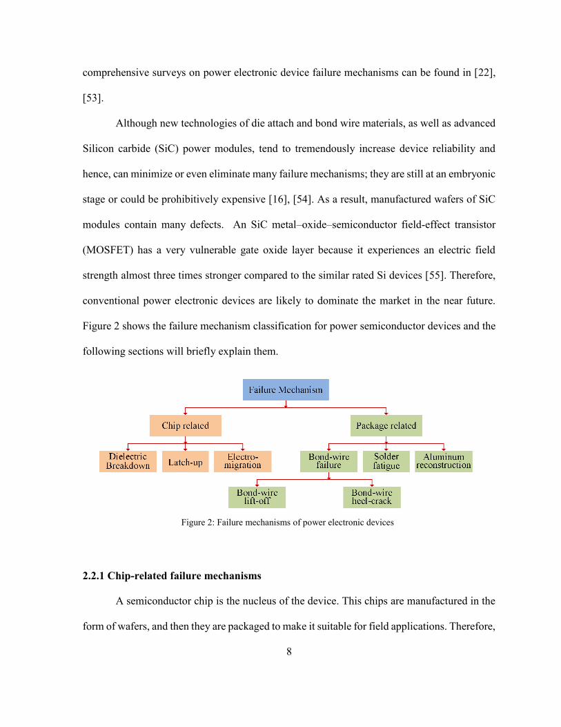
Figure 2 shows the failure mechanism classification for power semiconductor devices and the
following sections will briefly explain them.
2.2.1 Chip-related failure mechanisms
A semiconductor chip is the nucleus of the device. This chips are manufactured in the
form of wafers, and then they are packaged to make it suitable for field applications. Therefore,
Figure 2: Failure mechanisms of power electronic devices

9
the failures of the semiconductor devices can be classified into two major types: chip-related
and package related. Chip-related failure can be further classified into several types as
described below:
2.2.1.1 Dielectric Breakdown
We refer to a dielectric breakdown, which results from gate oxide degradation due to
accumulated defects, as a time dependent dielectric breakdown (TDDB) [52], [56]. Three
defect generation mechanisms are identified in [57]: impact ionization, anode-hole injection,
and trap creation. Catastrophic/acute dielectric breakdown occurs when the device experiences
severe electrical or thermal stress, i.e., over voltage and electrostatic discharge (ESD) [52],
[58]. Increased gate current and decreased drain current can be found in MOSFET after a
dielectric breakdown [43].
2.2.1.2 Latch-up
Latch-up can happen to both insulated-gate bipolar transistors (IGBT) and MOSFETs
if the parasitic thyristor or bipolar junction transistor (BJT) structure is triggered, causing a
loss of gate control. If the latch-up is not promptly removed, any high current will eventually
destroy the device [56], [59]. High dV/dt was identified as the cause of a MOSFET [60] and
IGBT [61] latch-up. In [62], operating the IGBT at a high temperature was the primary reason
that induced the latch-up.
2.2.1.3 Electro-migration
Metal migration, caused by high current density in silicon interconnects [22], [52], [58],
is the definition of electro-migration. As a result, voids form between metal connections and
cause increased resistance or an open circuit. Such degradation is rarely observed in power
electronic devices due to large contact areas [22].

10
2.2.2 Package-related failure mechanisms
Since high power applications widely use power modules, the failure mechanisms
discussed here are mainly consistent with power modules only. It should be noted, however,
these failure mechanisms may also be applicable to low power devices. Power modules are
usually constructed in multilayer structures, as shown in Figure 3. Silicon chips are soldered
onto a direct bonded copper (DBC) substrate that provides necessary electric insolation, and
the substrate is then soldered onto a base plate. Al bond wires are normally used to connect
different chips and form terminals. Three major failure mechanisms are reported in the
literature, namely bond wire failure, solder fatigue, and aluminum reconstruction [53].
2.2.2.1 Bond wire failure
Bond wire failures can be further classified into two types: (1) bond wire lift-off and
(2) bond wire heel cracking. The main reason for bond wire lift-off is the mismatch of a
coefficient of thermal expansion (CTEs) between Si and Al interfaces. During thermal cycling,
a crack initiates and propagates in the interface between the wire and device and finally leads
to a bond wire lift-off. Fracture fatigue is considered as the main reason for bond wire heel
cracking. Displacement at the top of a bond wire loop creates an alternation in the bending
Figure 3: Typical multilayer structure of a power module
11
angle when a device is subjected to thermal cycling. Fatigue by thermal cycling is rare in
advanced IGBT modules [53].
2.2.2.2 Solder fatigue
As shown in Figure 1, there are two solder layers in a typical power module, i.e., one
between the Si device and DBC and another between the substrate and baseplate. A larger CTE
mismatch in between the substrate and baseplate makes it more susceptible to solder fatigue.
Thermal and power cycling will create voids and cracks in solder-attached layers that
propagate as the thermal cycle increases [63]. The voids increase the thermal impedance,
resulting in a higher temperature in the die that accelerates the propagation of voids. In other
words, a positive feedback loop is formed between die temperatures and voids propagation.
Eventually, the large amount of heat can cause damage to the device. As stated previously,
overheating can be the root cause of latch-up and failing to turn on [64]. Hence, package-
related failures can sometimes induce chip-related failures.
2.2.2.3 Aluminum reconstruction
Aluminum reconstruction refers to the aging mechanism of the metallization layer
deposited on the silicon chips [65]. Different CTEs, between the aluminum and Si, induce
compressive and tensile stresses in the aluminum layer that can exceed the elastic limit and
cause aluminum reconstruction. This failure mechanism can be effectively prevented by using
a passivation layer [53].
A correlative table can be constructed based on the failure modes and the failure
mechanism occurs in an IGBT module to illustrate the potential locations of failure, causes,
and the parameters affected due to the failure [66]. They are summarized in Table I.

12
2.3 Conclusions
In field applications, power semiconductor devices or modules undergo one or more
failure mechanisms simultaneously. Therefore, it is common to occur both bond wire lift-off
and heel crack or die-electric breakdown and solder fatigue at the same time. As a result, it
becomes difficult to identify the underlying reasons behind the failures. However, there exists
several degradation detection techniques which can identify the aging of the devices, of course
having both pros and cons, and those methods will be discussed in the following chapter.
Table I Comparison between failure mechanisms [66]
Failure
mechanism
Location Causes Modes Parameter
affected
Time dependent
dielectric
breakdown
(TDDB)
Oxide
layer
1. Over voltage
2. High temperature
3. High electric field
1. Increased leakage
current
2. Loss of gate control
3. Short circuit
Vth
Latch-up
Silicon
Die
1. Over voltage
2. Irradiation
3. High electric field
1. Device burnout
2. Loss of gate control
VCEON
Hot electrons
Oxide
Oxide/su
bstrate
interface
1. High current density
2. Over voltage
High leakage currents
Vth
Bondwire/Solder
fatigue
Bondwire
/Solder
1. High current density
2. High temperature
Open circuit
VCEON
Delamination of
die
attach/Voiding
Die
attach
1. High current density
2. High temperature
Open circuit VCEON

13
CHAPTER 3
EXISTING DEGRADATION DETECTION & LIFETIME PREDICTION
TECHNIQUES
3.1 Introduction
Lifetime prediction or reliability analysis of power electronic devices has emerged as
one of the distinguished branches in engineering since the early 1950s [67]. The essence of
reliability analysis evolved from the electronic tubes’ failure that occurred during World War
II [68]. Since then, numerous methods and standards have been used toward the analysis of the
devices, components, and/or system failures that specifically occurred because of the electronic
or power electronic components. In 1956, “Reliability Stress Analysis for Electronic
Equipment”, TR-1100, contained a mathematical model based on the component failure rate.
In 1962, the first Military Handbook-217 (MH-217), which derived from this, was published
to standardize the test protocol [68]. Afterwards, a multiple version of MH-217 came out in
order to improve the reliability assessment models and keep up with the newest technology. It
made the MH-217 standards much more complex. Later, in the 1980s, industry specific models
derived from this handbook. Finally, these empirical data based lifetime models (MH-217F)
were formally cancelled due to the increased complexity in integrated circuits and components
[124]. The physics-of-failure (PoF) based models that developed in 1962 and gained popularity
in the 1990s have since been used extensively in the lifetime prediction of both power
electronics and micro-electronics [68]. The PoF identified that the root cause of failure
mechanisms was influenced by environmental stress and the empirical lifetime method
approaches identified the failure statistically. A constructive comparison between these two
methods is shown in Table II.

14
Generally, lifetime prediction methods for power electronic modules are twofold. The
first method is based on failure mechanisms. Although various failure mechanisms have been
identified, the existing lifetime prediction models mainly focus on package related failures.
Such models can be classified into two categories: (1) empirical models and (2) physics-of-
failure (POF) based models. Most of these models describe a number of cycles to failure (Nf)
as a function of failure-relevant parameters such as junction temperature swing (ΔTj) and mean
junction temperature (Tm). The second method is based on failure precursor parameters. This
method is an essential part of the prognostics and health management (PHM) approach, and is
always implemented in applications to provide a remaining useful life (RUL). Compared to
the first method, this method provides the remaining useful time in real-time units, such as
minutes, days, etc., rather than in the number of cycles to failure.
Table II Comparison between failure methods [68]
Method Advantages Limitations
Empirical
model
1. Reflects actual field failure rates
and defect densities
2. Can be a good indicator of field
reliability
1. Difficult to keep up-to-date
2. Difficult to collect good-quality field data
3. Difficult to distinguish cause vs effect for s-
correlated variables (e.g., quality vs
environment)
Physics-of-
failure
(PoF)
model
1. Modeling of specific failure
mechanisms
2. Valuable for predicting end-of-
life for known failure
mechanisms
1. Cannot be used to estimate field reliability
2. Highly complex and expensive to apply
3. Cannot be used to model defect-driven
failures
4. Not practical for assessing an entire system
Test data
1. Reflects the actual reliability
2. Test data can be collected and
applied before the system is
deployed
1. Translations to field stresses required, which
requires acceleration models and adds
uncertainty to the estimate

15
3.2 Failure mechanism-based lifetime prediction
Existing models mostly predict two failure mechanisms, namely, bond wire failure and
solder fatigue. It should be noted, however, that the models for each failure mechanism are not
mutually exclusive because both failure mechanisms are due to a CTE mismatch in the
interface areas. Indeed, some models are interchangeable. Generally, lifetime prediction
methods for power electronic modules are twofold. The first method is based on failure
mechanisms. Although various failure mechanisms have been identified, the existing lifetime
prediction models mainly focus on package related failures. Such models can be classified into
two categories: (1) empirical models and (2) physics-of-failure (PoF) based models. Most of
these models describe a number of cycles to failure (Nf) as a function of failure-relevant
parameters such as junction temperature swing (ΔTj) and mean junction temperature (Tm). The
second method is based on failure precursor parameters. This method is an essential part of the
prognostics and health management (PHM) approach, and is always implemented in
applications to provide a remaining useful life (RUL). Compared to the first method, this
method provides the remaining useful time in real-time units, such as minutes, days, etc., rather
than in the number of cycles to failure.
3.2.1 Bond wire failure models
As discussed in the previous section, bond wire failures can occur at a bonding interface
or bond wire heel. Different models of bond wire failures will be introduced in this section.
Empirical models will be introduced first, followed by the physics of failure models.
3.2.1.1 Empirical lifetime models
Empirical models were initially developed by statistically studying the test data of
accelerated aging experiments, which will be discussed in the next section. Due to different

16
test protocols and module types, the dominant failure mechanisms, observed for different
power electronic devices, are different. The following models are classified in the category of
bond wire failures because during the accelerated aging experiments from which these models
were developed, the dominant failure mechanism observed was bond wire failure. For this
reason, the accuracy of such models can only be guaranteed when used in situations similar to
the test conditions from where the models were “born”. One common feature of these models
is that they relate lifetime to junction temperatures.
An empirical lifetime model of an IGBT module is proposed based on the fast power
cycling results, in other words, accelerated aging based test results [69] as shown in equation
(1):
𝑁𝑓 = 𝐴 ∙ 𝛥𝑇𝑗𝛼 ∙ exp(
𝑄
𝑅∙𝑇𝑚) (1)
where R, being the gas constant (8.314 J/mol.K) and Tm in Kelvin make A = 640, α = -
5, and Q = 7.8×10⁴ J/mol.
Figure 4 is attached to illustrate the results obtained in [69] using equation (1). The
parallel shift is a clear indication of thermal mechanism, and hence, it was combined with the
Arrhenius approach.
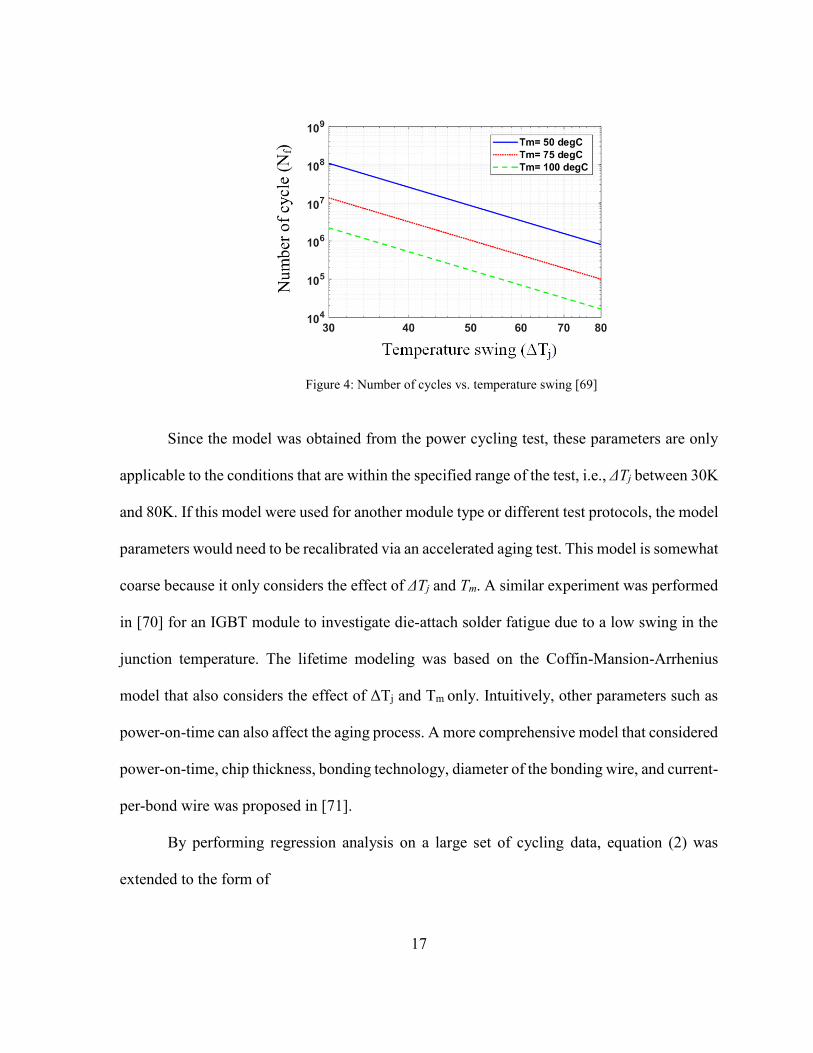
17
Since the model was obtained from the power cycling test, these parameters are only
applicable to the conditions that are within the specified range of the test, i.e., ΔTj between 30K
and 80K. If this model were used for another module type or different test protocols, the model
parameters would need to be recalibrated via an accelerated aging test. This model is somewhat
coarse because it only considers the effect of ΔTj and Tm. A similar experiment was performed
in [70] for an IGBT module to investigate die-attach solder fatigue due to a low swing in the
junction temperature. The lifetime modeling was based on the Coffin-Mansion-Arrhenius
model that also considers the effect of ΔTj and Tm only. Intuitively, other parameters such as
power-on-time can also affect the aging process. A more comprehensive model that considered
power-on-time, chip thickness, bonding technology, diameter of the bonding wire, and current-
per-bond wire was proposed in [71].
By performing regression analysis on a large set of cycling data, equation (2) was
extended to the form of
Figure 4: Number of cycles vs. temperature swing [69]

18
𝑁𝑓 = 𝐾 ∙ 𝛥𝑇𝑗𝛽1 ∙ exp(
𝛽2
𝑇𝑙𝑜𝑤) ∙ 𝑡𝑜𝑛
𝛽3 ∙ 𝐼𝛽4 ∙ 𝑉𝛽5 ∙ 𝐷𝛽6 (2)
Where, ton is the power on time, I is the current-per-bond wire, V is the blocking voltage,
and D is the bond wire diameter. Parameters β1 to β6 are obtained from statistical data. Like
any empirical model, the validity of the model is only guaranteed within the range of selected
data, and the authors of [71] also suggested using the model with caution.
3.2.1.2 Physics-of-failure-based lifetime models
The model with the simplest form within this category is probably the Coffin-Manson
model, which assumes that plastic strain is the main cause of the bond wire lift-off and the
elastic strain is negligible. Since the model emphasizes the effects of plastic strain, it is also
referred to as the plastic strain-based model [72]. The model is shown in equation (3) [73],
[74].
𝑁𝑓 = 𝐶1(𝛥𝜀𝑝)−𝐶2 (3)
Another form of equation (3), which was initially applied to bond wire failure and
presented in paper [53], is shown in equation (4). It can be obtained by substituting 𝛥𝜀𝑝 in (4)
by𝐿 ∙ 𝛥𝛼 ∙ 𝛥𝑇. It needs to be mentioned that this model is only valid when the peak temperature
does not exceed 120˚C. From the deduction procedure presented in [53], ΔT in equation (4)
should be the temperature swing at the bond wire-chip interface rather than the junction
temperature.
𝑁𝑓 = 𝑎(𝛥𝑇)−𝑛 (4)

19
The Coffin-Manson model is suitable for low cycle fatigue. As for high cycle fatigue,
the Basquin equation is used to describe damage induced by stress range Δσ [75]. This model
is presented in equation (5), where C1 and C2 are material-specific parameters.
𝑁𝑓 = 𝐶1(𝛥𝜎)−𝐶2 (5)
Another strain based model is shown in equation (6), where strain-intensity-factor
range ΔKε is selected for the failure metric [76]. This paper aims at investigating thermal
fatigue under low temperature fluctuation, i.e., 𝛥𝑇 under 40. The crack growth rate is
calculated from the strain intensity factor by Paris' law. It assumes that failure would happen
if a critical crack length is reached.
𝑑𝑎
𝑑𝑁= 𝐶(𝛥𝐾𝜀)
𝑛 (6)
𝑁𝑓(𝐼) =𝑤𝑝𝑙𝑐𝑟
𝑤𝑝𝑙(𝐼) (7)
Equation (7) shows an energy based lifetime prediction model for Al ribbon bonds
subjected to a heel crack failure mechanism [77], in which 𝑤𝑝𝑙𝑐𝑟 is the energy limit and 𝑤𝑝𝑙(𝐼)
is the energy dissipation per cycle under current I. The model assumes that the ribbon can
withstand a certain amount of energy dissipation before a sudden failure. In addition, the
effects of residual stress on the crack evolution were not considered in this model, which this
paper later proves to have a negative impact on the ribbon lifetime. A comparison of the
lifetime prediction between this model and the Coffin-Mansion model shows discrepancies.
Although the model itself seems logical, there could be some over simplifications or
misjudgments during model parameterization.

20
3.2.2 Solder fatigue models
Before introducing the lifetime prediction models, it is necessary to introduce the
failure criteria first. It is not necessary to introduce bond wire failure criteria because they are
self-evident; a bond wire fails when it is lifted or its heel cracks. As for fatigue, however, the
definition of failure corresponds to a point when a certain percentage of solder becomes
damaged.
3.2.2.1 Empirical lifetime models
An early attempt to empirically describe the lifetime of leaded solder subjected to a
thermal cycling test was proposed by Norris and Landzberg, and hence called the Norris-
Landzberg model, as shown in equation (8) [78]. This model was widely used for defining the
acceleration factor (AF) to map the accelerated lifetime test (ALT) time scale and lifetime in
the field application [79].
𝑁𝑓 = 𝐴 ∙ 𝑓−𝑛2𝛥𝑇−𝑛1 ∙ exp(𝐸𝑎
𝐾∙𝑇𝑚𝑎𝑥) (8)
In [80], this model was modified for lead-free solder material by a recalibration process
using experimental data. The modification added a new term to the original equation
considering the dynamic behavior of solder materials. This model is presented in equation (9),
where𝑐𝑜𝑟𝑟(𝛥𝑇) = 𝐴𝑙𝑛(𝛥𝑇) + 𝐵, A and B are material dependent constants, and c is a variable
dependent on a thermal cycling profile.
𝑁𝑓 = 𝐴 ∙ 𝑓−𝑛2𝛥𝑇−𝑛1 ∙ exp (𝐸𝑎
𝐾∙𝑇𝑚𝑎𝑥) [𝑐𝑜𝑟𝑟(𝛥𝑇)]−1/𝑐 (9)
Another modified version of equation (9) is presented in [81], in which the frequency
term is replaced by the parameter thot representing the time per cycle that the device is hot. The
model is presented by equation (10).

21
𝑁𝑓 = 𝐴 ∙ (1
𝑡ℎ𝑜𝑡)−𝑛2𝛥𝑇−𝑛1 ∙ exp(
𝐸𝑎
𝐾∙𝑇𝑚𝑎𝑥) (10)
3.2.2.2 Physics-of-failure (POF) based lifetime models
As mentioned earlier, a clear boundary does not exist between solder fatigue models
and bond wire failure models when the materials’ physical properties are considered. The first
model to be introduced is essentially the same as equation (3), but written in a more institutive
form as shown in equation (11) [82] - [84]:
𝑁𝑓 =𝐿
𝑎(𝛥𝜀𝑝)𝑏 (11)
Where, L is the length of the solder interconnect, Nf is the number of cycles needed for
the crack length to reach L, 𝛥𝜀𝑝 is the average accumulated plastic strain per cycle, and a and
b are material-dependent constants.
Fig 5 has been included using equation (11) to show the correlation between L and Nf
for two plastic strain values (𝛥𝜀𝑝) of an SnAg solder joint. Constants, a and b are given as
0.00562 and 1.023 for SnAg solder [85]. Since the failure is defined by the moment when the
crack length reaches 20% of the solder thickness, the maximum value of L used in the equation
should be 0.1mm because the solder thickness is 0.5 mm. According to these plots, the number
of cycles is strongly related to the accumulated plastic strain value. However, this value of 𝛥𝜀𝑝
is a function of the temperature swing (ΔT) and the mean temperature (Tm) of the experiment
[85] – [87]. Hence, once the operating condition is defined, i.e., the mean temperature and the
temperature swing are known, the number of cycles can be estimated in order to study the
solder fatigue phenomenon.

22
Another plastic strain based model has been described in [88]. Similar to (3), its validity
relies on the assumption that elastic strain has little effect on solder fatigue. A shear strain-
based model was proposed by Solomon [89], shown in equation (12), where C and n are
material dependent constants, and Δγp is the plastic shear strain range.
𝑁𝑓 = 𝐶(𝛥𝛾𝑝)𝑛 (12)
A model to predict large solder joint failure is given in (13), where L is the lateral size
of the solder joint, Δα is the CTE mismatch, ΔT is the temperature swing, c is the fatigue
exponent, x is the thickness of the solder, and γ is the ductility factor of the solder [53].
𝑁𝑓 = 0.5(𝐿𝛥𝛼𝛥𝑇
𝛾𝑥)1/𝑐 (13)
Strain-based solder fatigue models are criticized as inadequate, because the solder
lifetime may also be a function of stress. Therefore, an energy based approach is considered as
an alternative [90]. The most widely used definition of energy to determine failure is called
strain-stress hysteresis energy. Similar to the energy based models for bond wire failures, the
Figure 5: Number of cycles vs. crack length.

23
rationale of energy based models is shown in equation (14), where Ef is the total energy to
failure, Ec is the energy per cycle.
𝑁𝑓 =𝐸𝑓
𝐸𝑐 (14)
An early attempt was presented in [91] to analyze the data for 60Sn-40Pb solder. A
proposal for a recent application to estimate the lifetime of an IGBT module in an automotive
application is shown in [92], where the lifetime of the module under a mission profile was
estimated with the total known deformation energy (energy to failure).
So far, one may have found that all POF based models have some parameters to be
determined. In theory, module geometry and material properties are necessary to determine the
unknown parameters. Therefore, it might be more appropriate to categorize them as semi-
empirical models since they also need parameterization.
3.2.3 Real-time lifetime estimation
Now that we have the lifetime prediction models as mentioned above, one may expect
to estimate the lifetime or level of degradation of a power device in real applications; however,
some obstacles still need to be tackled. The first question is which type of model do we use,
the empirical model or POF model? In both experiment and simulation, temperature is more
easily accessible than mechanical quantities, i.e., plastic strain. Parameters such as plastic
strain and strain-stress hysteresis energy are usually obtained from thermo-mechanical finite
element analysis (FEA). FEA not only requires the temperature profile of the device, but also
needs the material properties and device geometry. In other words, choosing POF models
requires one more intensive simulation step than choosing the empirical models. This is
because the empirical models directly utilize device temperature to estimate the number of
cycles to failure. Whichever model is chosen, this next problem is inevitable. The models only

24
take specific conditions into account, i.e., a fixed mean junction temperature and temperature
swing, but power modules experience a time varying load profile. To address this problem,
Miner’s rule, which says the damage effect can be linearly accumulated, is commonly
employed [72], [93] – [96]. The general form of Miner’s rule is shown in equation (15), where
LC is the lifetime of the device that has been consumed in a percentage, nk is the actual cycle
of a certain operating point, and Nfk is the cycle to failure of the operating point.
𝐿𝐶 = (𝑛1
𝑁𝑓1+
𝑛2
𝑁𝑓2+
𝑛3
𝑁𝑓3+⋯+
𝑛𝑘
𝑁𝑓𝑘) × 100% (15)
To obtain nk at a certain operating point, we need cycle counting methods to extract
useful information from the device’s temperature history. There is not a uniformed definition
to count the thermal cycles from a random temperature profile. Various cycle counting
methods are found in [97]. The most widely used one is the rain-flow counting method [98]
that groups local minima and maxima to an equivalent cycle. In [92], several definitions of a
temperature cycle are discussed. The cycle counting results of different definitions from the
same temperature profiles are slightly different and result in deviations in the lifetime
prediction results. Therefore, selecting a proper cycle counting method can help improve the
estimation accuracy. However, in the literature, there is no comprehensive comparison of
which method leads to a better estimation under what condition. Conventionally, the rain-flow
method is used off-line because it requires the entire load profile history. As it can only process
data in chunks, if requires a large data storage system that is inconvenient to implement in a
real-time application. To tackle this problem, a real-time rain-flow counting approach is
proposed in [93] using a recursive algorithm.

25
3.3 Failure precursor-based lifetime prediction
Failure precursors are the parameters that change with device degradation, and thus can
indicate an imminent failure. The literature identifies various failure precursors of power
electronic devices by accelerated aging tests. Typical ones are summarized below.
3.3.1 Failure precursors of power electronics devices
The most significant aging indicator for power MOSFETs [99] is an increase in ON-
state resistance. We find similar observations in [100] – [102]. The authors in [103] concluded
that a power MOSFET completely fails if the initial value of RDSON increases by 10%-17%.
Increased gate threshold voltage of an aged power MOSFET was discovered in [104], [105].
In [62], increased threshold voltage was observed in an aged IGBT. The ringing characteristic
is used as an indicator of IGBT aging in a motor drive in [106]. Brown et al. [107] identifies
the turn-OFF time as an indicator of an IGBT latch-up. In addition, the rise time and fall time
increase with the level of aging as reported in [108]. ON-state voltage has been identified as
an IGBT failure precursor in [9], [62], [109] – [113]. However, this quantity does not
monotonically increase or decrease with respect to degradation. In [62], the ON-state voltage
was reported as going down due to aging, while in [109], [110], an increase was reported. In
[9], a decrease was observed followed by an increase in collector-emitter voltage (VCE). This
seeming contradiction lays in two competing aging mechanisms, namely, solder fatigue and
bond wire degradation. The IC-VCE characteristic curve has a negative temperature coefficient
below a crossover and a positive one above it. Solder fatigue will increase the thermal
impedance, and hence, increases the temperature. If the IGBT is operating below the crossover,
an increased temperature will result in a decreased VCE, as observed in [9], [62]. However, if
bond wire failure becomes dominant or the IGBT is operating above the crossover, an

26
increased VCE should be observed. It might be concluded that at a low collector current, VCE is
more sensitive to temperature, while at a high collector current, VCE is more sensitive to bond
wire degradation.
Experimental results obtained from the accelerated aging test conducted in [114]
support the above statement. In this paper, an IGBT bond wire lift-off was studied and VCE
was going up with the bond wire lift-off. Thermal stress was up to 120°C for the die, and it
was induced from a power cycling test. A junction-to-case thermal impedance increase has
been characterized as one of the precursors for solder layer degradation of the IGBT power
module in [115]. Apart from the thermal impedance, the temperature of the chip surface also
increases with the level of solder fatigue.
3.3.2 Precursor parameter measurements
Precursor parameter measurement is indispensable to predict the RUL, but such a
measurement is confronted with many challenges, especially in a live converter. Aside from
the additional sensors needed to perform measurements and corresponding change in the
circuit structure, the high resolution measurement needed for the sensors to extract a small
deviation from a high voltage high current operating context is computing intensive. Moreover,
a high switching frequency induced noise imposes a burden on measurement accuracy, and
most failure precursors depend on the operating point (e.g., temperature and load current) that
must be taken into account during measurement. More importantly, it is preferred that such a
measurement does not alter the normal operation of the system. An advanced gate drive with
the capability to measure various voltages and currents within the device has the potential to
resolve the aforementioned difficulties [116] – [119], but their applications in prognostics of
power electronic devices have yet to be explored.

27
Most of the existing precursor measurement methods require a measurement window
inserted in the converter’s normal operation. For example, in [120], on-line monitoring of an
IGBT module under power cycling stress was studied. An H-bridge inverter comprising four
IGBTs was stressed by thermal cycling induced by low frequency PWM power cycling. A
periodic measurement of VCE was carried out at the fixed current (110A) and the fixed junction
temperature (125ºC). To achieve this, the normal inverter operation was interrupted by a
particular switching pattern that made the current and junction temperatures vary around the
fixed values. Then, the values at the fixed operating point were obtained by an interpolation.
A similar accelerated test was conducted in [121] on an H-bridge converter constructed
from high power IGBTs. Aging was induced by a power cycling method with a peak current
of 890A while the IGBT was attached to the cooling system. Glycol with water was used as
the liquid coolant. The authors defined the VCE and the anti-parallel diode’s forward voltage
drop (Vf) as the aging precursor and monitored them online during the converter operation.
Although the device under test (DUT) was the IGBTs on the first leg, the test set-up used in
this paper initiated degradation on devices of the second and third leg but the rate of
degradation was at a much slower compared to the first leg.
In [43], Nasrin proposed a way of utilizing spread spectrum time domain reflectometry
(SSTDR) to evaluate resistance-based degradation in power converters. Impedance
discontinuities can be detected by observing the correlated output from SSTDR. In general, an
abrupt change in impedance will result in a positive or negative peak in correlated output. In
turn, the peak value can be used to back calculate the impedance. However, this method can
only work when the device was isolated from the converter or the converter is not pulsed with
PWM signal. In addition, this method limits the application to the rated voltage of the SSTDR
28
hardware (1000V) since the test points are located at the drain-source interface of the power
devices. Therefore, it is not feasible to apply SSTDR signal from the drain or collector terminal
while the converter is live.
3.3.3 Remaining useful life prediction
A failure precursor-based lifetime prediction requires a predefined failure threshold,
i.e., 30% increase of RDSON [100]. This lifetime prediction method is actually a part of the
prognostic approach. In general, prognostic algorithms can be classified into a model-based
approach, data-driven approach, and hybrid approach. Using a hybrid approach has the
following advantages: (1) easy to implement due to the simplicity of the model, (2) ability to
capture the complex systems, thanks to data-driven methods, and (3) ability to identify
intermittent failures. In [104] and [122], this approach was applied to MOSFET and IGBT,
respectively, where an empirical model was obtained by offline regression analysis and then
fitted into an online prediction algorithm (in these cases, particle filtering), which then further
tuned the model by tracking the system behavior. The RUL was predicted by comparing the
failure precursor and the end-of-life threshold. A similar method was later adopted in [64],
where a two-step prognostic approach was proposed. In the first step, Mahalanobis distance
(MD) was used to detect anomalies in the device. If an anomaly was observed, particle filtering
was used to determine RUL. Compared to the failure mechanism-based predictions, the
advantage of this method is that knowledge of the entire history of the device is not mandatory.
Instead, a certain amount of discrete measurement of failure precursor is sufficient. The major
limitation of this method though, is that the empirical model was developed from an
accelerated aging test, which means the RUL prediction was given in an accelerated time scale.
Therefore, to use this method in the field application, a mapping from the accelerated time
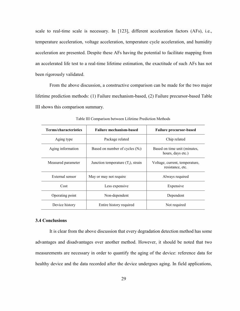
29
scale to real-time scale is necessary. In [123], different acceleration factors (AFs), i.e.,
temperature acceleration, voltage acceleration, temperature cycle acceleration, and humidity
acceleration are presented. Despite these AFs having the potential to facilitate mapping from
an accelerated life test to a real-time lifetime estimation, the exactitude of such AFs has not
been rigorously validated.
From the above discussion, a constructive comparison can be made for the two major
lifetime prediction methods: (1) Failure mechanism-based, (2) Failure precursor-based Table
III shows this comparison summary.
3.4 Conclusions
It is clear from the above discussion that every degradation detection method has some
advantages and disadvantages over another method. However, it should be noted that two
measurements are necessary in order to quantify the aging of the device: reference data for
healthy device and the data recorded after the device undergoes aging. In field applications,
Table III Comparison between Lifetime Prediction Methods
Terms/characteristics Failure mechanism-based Failure precursor-based
Aging type Package related Chip related
Aging information Based on number of cycles (Nf) Based on time unit (minutes,
hours, days etc.)
Measured parameter Junction temperature (Tj), strain Voltage, current, temperature,
resistance, etc.
External sensor May or may not require Always required
Cost Less expensive Expensive
Operating point Non-dependent Dependent
Device history Entire history required Not required

30
the power electronic devices experience gradual degradation over the course of operation and
it will require years for a device to experience significant aging that can be detected by the
existing techniques. That is why a method is necessary in order to quicken the aging of the
device so that the degradation can be studied and detection technique can be proposed within
few days instead of waiting for months, even years. This technique is termed as accelerated
aging method and will be discussed in the following chapter.

31
CHAPTER 4
ACCELERATED AGING METHODS
4.1 Introduction
An accelerated life test is an indispensable technique for reliability oriented issues. It
can be performed for different purposes such as testing device reliability, investigating failure
mechanisms, identifying failure precursor parameters, parameterizing lifetime prediction
models, etc. In general, power cycling and thermal cycling are most commonly adopted
accelerated aging methodologies. These methods aim at qualifying chip and package related
reliability issues. During power cycling tests, devices are heated by the power loss generated
inside the package; also referred to as active temperature cycling. On the other hand, thermal
cycling created externally by virtue of a thermal chamber is called passive temperature cycling.
Additionally, chronic thermal and electrical overstresses are also reasons for immediate
failures. These methods have been used separately or in combination to study the reliability of
power devices. This chapter presents existing accelerated tests. The classifications are purpose-
based.
4.2 Device qualification tests
Qualification tests are widely used by semiconductor manufacturers to test the
reliability of their products [125] – [128]. Many industrial standards exist, i.e., IEC60747,
IEC60749, IEC60068, AEC‐Q101, and JESD‐47. An example of the Semikron test standards
is shown in Table IV [125]. These standards provide a common platform to compare and
improve the quality of devices. However, comparison between the products from different
manufacturers is not straightforward because the test standards employed by different

32
manufacturers are diverse. In addition, most standards are for general purposes and hence, may
not be well suited for specific usage profiles.
4.3 Test for exploring failure mechanisms or failure precursors
Aside from industrial standards, other accelerated tests that target specific failure
mechanisms or precursors can be found in the literature. In the 1990s, a few projects on
enhancing the reliability of IGBT modules for traction applications were initiated in European
countries. Typical projects were Leistung Elektronik Systemtechnik Informations Technologie
(LESIT) (1994–1996) and reliability of advanced high power semiconductor devices for
railway traction applications (RAPSDRA) (1996–1998).
These projects proposed some standardized accelerated tests for IGBT modules in
traction applications and empirical lifetime prediction models were originally developed
Table IV Standard tests for the qualification of SKiM modules [125]
Test standard Test conditions Description
IEC 60747 1000 h, VCE = 95% VCEmax,
Tc = 160 °C High temperature reverse bias
test (HTRB)
IEC 60747 1000 h, ± VGEmax,
T = 175 °C
High temperature gate bias
(HTGB)
IEC 60068-2-67 1000 h, 85 °C, 85 % RH,
VCE = 80 % VCEmax (maximum value
of VCEmax =80V)
VGE = 0V
High humidity high temperature
reverse bias (THB)
IEC 60068-2-2 1000 h, + 135 °C High temperature storage (HTS)
IEC 60068-2-1 1000 h, - 40 °C Low temperature storage (LTS)
IEC 60068-2-14
Test Na
500 cycles, - 40 °C to + 125 °C Thermal cycling (TC)
IEC 60749-34 25,000 load cycles, ΔTj = 110 K Power cycling (PC)
IEC 60068-2-6
Test Fc
Sinusoidal sweep, 10g, 2 h per axis
(x, y, z) Vibration
IEC 60068-2-27
Test Ea
Half sine pulse, 100g,
3 times each direction (x, y, z) Mechanical shock

33
therein. They exclusively studied package related failure mechanisms, i.e., bond wire failures
and solder fatigue. The LESIT project purposed a “fast power cycling test” for IGBT modules
in traction applications [69]. The IGBT under test was mounted on a water-cooled heat sink
with a constant gate voltage and a periodical (2sec) load current. The power cycling test was
aimed to create a swing in junction temperature Tj that caused device degradation. More
comprehensive test conditions (purposed by RAPSDRA) are in Table V [129] in which three
test protocols are defined. It was found that bond wire failures are more susceptible to power
cycling 1 (fast cycling) while solder fatigue is generally caused by slow cycling, namely power
cycling 2 and thermal cycling. This test standard and its variants were used extensively to
evaluate the reliability and failure mechanisms of different IGBT modules [129] – [134].
An accelerated aging system to explore an intrinsic degradation mechanism on a power
semiconductor is proposed in [135]. The system is aimed at studying intrinsic degradation
precursors related to a device’s physical properties. The unique feature of this system is that it
isolates electrical overstress from thermal overstress. Therefore, the internal temperature of the
Table V RAPSDRA test protocols [129]
Reliability test Test conditions Estimated testing time
Power cycling 1 (active) Tmin=55˚C
ΔT=50˚C, 70˚C
Ic=Icnom, tcycl=3sec
3,000,000*3sec=104days
Power cycling 2 (active) Tmin=55˚C
ΔT=50˚C, 70˚C
Ic=Icnom, tcycl=1min
100,000*1min=70days
Thermal cycling (passive) Tmin=25˚C
ΔT=105˚C, 125˚C
tcycl=4min
Max.10,000*4min=28days

34
test subject can be controlled to avoid package related failures by eliminating thermal cycling
and controlling the highest junction temperature within the rating limits.
The degradation precursor for IGBT was studied in [62] where accelerated aging, based
on failure modes, mechanisms, and effects analysis (FMMEA) was performed. Selected
parameters were monitored in-situ. Thermal-electrical stress was induced by removing the heat
sink of IGBT under test so that it could heat itself. The gradual aging process of IGBT was
implemented by introducing a thermal feedback loop that regulates the IGBT case temperature
within a hysteresis bound. Aging was stopped when any latch-up occurred. The test bed was
composed of an oscilloscope recording transient data, a function generator generating gate
signals, programmable power supplies, and a data acquisition module. A similar aging
technique was used in [106], where the junction temperature was set at 125% of the maximum
operational junction temperature defined by the manufacturer. After latch-up was observed,
the transistor was turned OFF for recovery and then subjected to aging again. The level of
aging was described by the number of latch-up events. This methodology was used in [107]
with a slight modification that decreased the set point of the junction temperature after each
latching occurred when doing repetitions. The rationale behind this set-point reduction was
that the thermal resistance increases due to die attach deterioration.
In order to obtain the failure precursor and mechanism of a super-capacitor, an
accelerated test was conducted in [136]. Experimental results of this paper demonstrate that
the capacitor samples failed once the temperature increased to 155°C. The degradation level
was defined in terms of loss in capacitance and an increase in equivalent series resistance
(ESR). The super-capacitor was considered a complete failure when there was a 30% loss in
capacitance and the ESR increased by 100%.
35
4.4 Tests to verify condition monitoring methods
The ultimate goal of monitoring any condition is to detect early signs of failures in real
applications and schedule maintenance accordingly, in order to prevent unexpected outages.
However, when designing these methods, they have to be tested and verified under accelerated
test conditions. This type of accelerated test only needs to generate parameter degradation;
thus, the effectiveness of the method can be tested within a reasonable time span. In other
words, the main objective is to validate the condition monitoring method, and hence, the way
to perform the accelerated aging test is trivial as long as the precursor parameter of interest
exhibits measureable deviation with the proper trend. Therefore, all the aforementioned
accelerated aging methods can be used for this purpose. However, they can be unnecessarily
complex for simply generating parameter variations and a simpler alternative might be the so-
called DC aging.
In [28], MOSFETs were placed in the environmental chamber with constant gate
voltage and drain-source voltage, and a resistive load was connected to the source. A higher
drain-source voltage was used when a higher level degradation was expected. This test setup
did not resemble the real life condition; however, it increased the ON-state resistance of the
MOSFETs, which was sufficient to verify the method to measure the MOSFET ON-state
resistance in the live converter proposed in this paper. In paper [137], a thermal cycling was
applied to high-power MOSFETs. Those MOSFETs were placed in a temperature chamber
where the temperature was -55°C. A dc current was used to heat the MOSFETs to about 100°C
within 3 minutes; it held the temperature for 3 minutes, and then removed the dc current so the
device temperature dropped to the chamber temperature within 2 minutes.
36
Another thermal cycling based accelerated aging was accomplished in [103] where the
failure was identified as soon as the gate control was lost. Degradation was induced in the
device in three different conditions. The drain current was maintained at 5.2A, and the junction
temperature was 240°C, 220°C, and 210°C, respectively. The reliability of the power electronic
components (IGBT and MOSFET) of a motor drive was investigated in [138]. The temperature
of the environment was maintained at 85°C and humidity was 85%. At this condition, the
leakage current and ON-state resistance of the MOSFET increased significantly during any
power interruptions, but the IGBT did not show any sign of aging. A similar accelerated test
was performed in [139]. The only difference between these two tests was the input power
interruption that was given in the later experiment for a shorter time period and followed by
an over voltage situation. Both test results show that the environmental condition acted as a
positive feedback to accelerate the aging.
4.5 Tests considering mission profiles
A common feature of the aforementioned accelerated aging tests is that the DUTs were
under uniform periodic stress. In contrast, in the field applications, the devices undergo random
loading conditions. In order to compensate for this inconsistency, accelerated aging tests could
be employed dedicated to expose any devices to the conditions close to the field applications.
An active aging test bench that reproduced constraints similar to an automotive application
was recently proposed in [140]. In this paper, thermal coupling is considered because the
confined space makes this phenomenon significant. A driving cycle with given torque and
velocity was converted into switching and conduction losses of IGBTs and diodes. Because
the test bench could not produce any switching loss, the conduction loss during the test was set
equal to the sum of switching and the conduction losses were calculated from the driving cycle
37
profile. The DUT was mounted on a water-cooled heat sink. The power cycling was composed
of a 15s heating phase with a current that produced the desired conduction loss and a 30s
cooling phase without current injection.
A power cycling test bench for IGBT, used in wind applications, is presented in [141].
A low frequency (slip frequency) operation of the rotor side inverter was considered to be the
main source of the device degradation. The main feature of this test bench is that it varies load
current frequency with a given RMS value. With a certain load profile, the device temperature
can be collected by the data acquisition system. With the measured temperature profile, the
lifetime can be estimated using a lifetime model.
Accelerated lifetime testing has not only been carried out to estimate the lifetime of
IGBTs and MOSFETs but also for the lithium-ion capacitors [142], metallized film capacitors
[143], lithium-ion batteries [144], capacitors used for storing energy in particle accelerators’
power converters [145], and so on. Paper [146] proposed a strategy for designing an accelerated
aging test for IGBT solder fatigue. The goal is to find how many cycles are needed in an
accelerated aging test in order to create the same damage in the real condition. The general
procedure is summarized as follows. Step 1 - experimentally determine the number of thermal
cycles before failure occurs for a given aging methodology. Step 2 - use the test specifications
in conjunction with finite element simulation to find out the total energy (mechanical)
dissipated in the solder layer. Final step - another simulation based on the mission profile was
performed to find out the time period during which the dissipated energy equaled the total
energy obtained in the previous simulation. The assumption behind this methodology is that
the same dissipated energy results in the same degradation level regardless of the time span.

38
In view of the above discussion on various accelerated test methods, there is no
deniable fact that the junction temperature (Tj), ON-state resistance (RDSON) for MOSFET, and
VCEON for IGBT are the most commonly monitored parameters in condition monitoring of
power semiconductor devices. It is quite evident that RDSON and VCEON measurements are more
straightforward and easier compared to the Tj measurement. Since the junction of a power
device is not directly accessible in field applications, there exist several techniques in order to
estimate the junction temperature. Following section discusses these techniques of estimating
junction temperature.
4.6 Junction Temperature Measurement Methods
The reason that the temperature of the device junction is a crucial quantity where
reliability is concerned is manifold. During all accelerated aging tests, it is necessary to obtain
the device junction temperature, and the junction temperature is a part of the test protocol as
discussed above. In addition, many failure indicators such as VCE are sensitive to temperature,
and therefore, it is necessary to compare them at a fixed temperature to rule out the thermal
effect. The junction temperature of the device is also an important metric for thermal
management and condition monitoring, and the reliability assessment standards (such as
Military Handbook 271) estimate reliability based on the device temperature. This section
summarizes methods used to determine the device junction temperature. In general, the
junction temperature can be measured directly or indirectly. Direct methods are accurate but
intrusive, while indirect methods have moderate accuracy but are non-intrusive.
4.6.1 Direct measurement methods
Direct measurement requires temperature sensors located on the die, which is usually
inconvenient because the chip surface of a power module is not always accessible. However,
39
in laboratory conditions, such direct measurements are always performed to provide the
baseline data that verify the indirect measurement methods. A thermocouple is one widely used
type of temperature sensor for direct temperature measurement. Another direct method is the
optical method [147, 148]. The advantage of using an optical sensor is that it has both good
dynamic behavior and electric insulation that allows temperature measurement in high voltage
conditions. The limitation of a thermocouple and optical fiber is that only a single point (rather
than temperature distribution) can be obtained. An IR camera can be used to measure
temperature distribution as well, but the devices need to be opened and painted with black paint
to increase the emissivity.
4.6.2 Indirect measurement methods
4.6.2.1 FEM Method
The finite element method (FEM) is a powerful tool to determine the device junction
temperature. It can precisely simulate the chip temperature and spatial temperature distribution
if a proper mesh is developed. This method is time-consuming and computationally inefficient,
and thus, is not well suited to real-time temperature acquisition. However, high accuracy makes
this method useful in many occasions such as calibrating compact device thermal models and
providing the baseline temperature to determine the accuracy of other temperature
measurement methods. A study has been performed based on FEM in [149] in order to identify
the influence of a direct bond copper (DBC) metal trace layout in an IGBT module. The
simulation result shows the metal trace has larger area experiences with higher thermal stress.
4.6.2.2 TSEP Method
The most commonly used method to measure junction temperature indirectly is to use
a temperature sensitive electrical parameter (TSEP) [64]. As for IGBT, VCE at a small current

40
(several tens to hundreds milliamps) is always chosen as the TSEP. This method requires the
availability of junction temperature vs. VCE curve at a small calibration collector current.
During the calibration, the IGBT temperature is controlled by an external heating system, i.e.,
a temperature chamber, to obtain VCE,sat as a function of the junction temperature [150]. In
practice, the collector current during an accelerated test is much higher than the calibration
current. Therefore, a measurement window needs to be inserted into the IGBT normal
switching pattern to facilitate the temperature measurement. The measured current is
maintained as small as possible to minimize generated heat. In order to eliminate the need for
introducing the measurement window, which is not always feasible, VCE at a high current was
chosen as the TSEP in [151]. It is worth mentioning that VCE at a small current has a negative
temperature coefficient but a positive temperature coefficient is observed at a large current. In
[151], this phenomenon is explained by two competing factors, namely a PN junction with
dVCE/dTj<0 and a resistor with dVCE/dTj >0. In [152], a neural network is used for a junction
temperature estimation in which both VCE at a large current and IC are chosen as model inputs
and Tj is the output. A comparison between results from a neural network and from a
conventional polynomial curve fitting showed the superiority of this method. Compared to VCE
at a small current, a large current would amplify the effect of resistance. Therefore, bond wire
failure, which increases the resistance, will lead to an inaccuracy in the temperature
estimations.
In [153], the junction temperature was estimated by a short circuit current. Although it
was shown in this paper that a short circuit current is sensitive to junction temperature, it may
not be appropriate to use this method in real applications for several reasons. A short circuit
current will increase device self-heating, and hence, accelerates degradation that is

41
counterproductive to condition monitoring or thermal management. In addition, real converters
are all equipped with a short circuit protection mechanism, and removing the protection circuit
in favor of temperature measurements can hardly be justified. Moreover, from the examples
given in this paper, an additional IGBT is needed to measure each IGBT temperature, which
is very uneconomical. Another example of choosing VCE as the TSEP in a multi-die IGBT
module is found in [154]. The unique feature of this paper is that the authors have correlated
the case temperature of the IGBT module in order to find a direct relationship to the junction
temperature. Their results show that the correlation between the junction temperature (Tj ) and
case temperature (TC) gives the best match when TC is measured very close to the terminal lead
or package side. However, if the case temperature is used to estimate the junction temperature,
the measurement error becomes a little higher because once the IGBT module starts heating
up, the temperature distribution in the different die’s baseplates becomes non-uniform.
In addition to TC, IC and VCE have been identified as the failure precursors in [155]
where the authors performed the reliability analysis for the IGBTs usually used in an all-
electric vehicle. Other TSEPs include gate threshold voltage Vth and saturation current Icss [25].
In [156], dIce/dt and the trans-conductance are chosen as the TSEP for IGBT. A similar study
for the MOSFET junction temperature estimation was conducted in [157], where dIds/dt at a
constant Vgs was identified as the TSEP. In [158], Vth is considered as the TSEP in order to
measure the junction temperature because the experimental results illustrate that the threshold
voltage shows superior sensitivity compared to the body-diode forward voltage (VSD) of the
MOSFET. Since the calibration of TSEPs is performed under a homogenous chip temperature
while the temperature gradient is observed during active self-heating, discrepancy between the
measured and actual temperature is unavoidable [159]. Indeed, the temperature at the central
42
chip is normally higher than those of the corners and edges. Therefore, the severity of the
problem depends on how significant the effect that the chip geometry has on the temperature
measured by the TSEPs [160]. Specifically, a larger chip dimension tends to have a larger
measurement error. These methods are suitable for single chip modules or discrete devices, but
might be questionable for multichip module temperature measurements. For a multichip
module, the temperature measured using this method is actually the average junction
temperature of all chips. However, temperature distribution of different chips is hard to obtain
and can contribute to a localized failure.
4.6.2.3 Thermal Test Chips
Originally developed for thermal characterization of electronic packages [161], thermal
test chips (TTC) can also be used for chip temperature measurements. Commonly used TTCs
are diodes and resistors. As for diodes, forward voltage is sensitive to temperature, and hence,
can be used for temperature estimation. The calibration of temperature versus forward voltage
consists of a linear or polynomial fitting depending on the temperature range. A resistor is very
similar to the diode in terms of calibration, except that resistance is used as the temperature
sensitive parameter. In [162], a string of diodes are fabricated on the IGBT chip surface for
the temperature measurement. The disadvantage of this method is that the diodes or resistors
will degrade along with the device usage. Therefore, the accuracy of the measured temperature
will deteriorate over time.
4.6.2.4 RC Thermal Models
Another indirect method is using a compact device thermal model to estimate the
junction temperature. Thermal models are also used to obtain temperature waveforms over a
certain mission profile. A simple type is a resistor-capacitor-based thermal model [163] –

43
[165]. This RC type model can be further classified into the Cauer type and Foster type, which
are shown in Figure 6 [163] – [165].
The parameters of the Foster model are normally provided in the device datasheet by
manufacturers, and hence, can be employed conveniently. However, the thermal resistance
given in a datasheet considers the worst case scenario, which means that an offset accounting
for the device degradation is included. This could lead to a pessimistic estimation of junction
temperature. Direct use of datasheet parameters leading to junction temperature estimation
with poor tolerances was reported in [166]. The parameters of the RC thermal network can
also be obtained by either a FEM or by fitting the model to an experimentally measured
transient thermal impedance curve.
Parameterization of an RC compact thermal model involves fitting a multi-exponential
equation (16) to a device temperature impulse response with a zero initial condition.
(a)
(b)
Figure 6: RC thermal models (a) Cauer (b) Foster [163] – [165].

44
Zstep(t) = ∑ Rthi(1 − e−αit)N
i=1 (16)
A more comprehensive form of this model for a multi-chip module considering the
thermal coupling effect is shown in equation (16), where the diagonal elements are self-thermal
impedance and the off-diagonal elements are mutual thermal impedance [167].The
parameterization of equation (17) requires n experiments, where n is the number of chips of a
power module.
[T1⋮Tn
] = [Z11 ⋯ Z1n⋮ ⋱ ⋮Zm1 ⋯ Zmn
] [P1⋮Pn
] + TAmbient (17)
4.6.2.5 Heat Diffusion Equation based Methods
The advantage of an RC model is that it can be conveniently incorporated in circuit
simulators. However, a highly accurate model requires complex 3D finite element simulation,
which is time-consuming. An alternative way involves solving a heat diffusion equation. The
three-dimensional heat diffusion equation of isotropic material can be written as [166]:
𝑐𝜌∂𝑇
∂𝑡− ∇ ∙ (𝑘∇𝑇) = 𝑞𝑖𝑛𝑡 (18)
It is not always straightforward to solve these equations analytically. Approaches to
solve such equations can be found in [124], [168] and the references therein. In addition to an
analytical solution, equation (18) can also be discretized into a set of equations describing the
temperature of each node. This approach has been implemented in conjunction with a model
order reduction approach in [124]. Knowing the junction power dissipation and ambient
temperature, the device junction temperature can be easily calculated using the thermal model.
A major limitation of this approach is that the change of thermal impedance due to solder
degradation is not considered. Therefore, a periodic recalibration is necessary in order to use
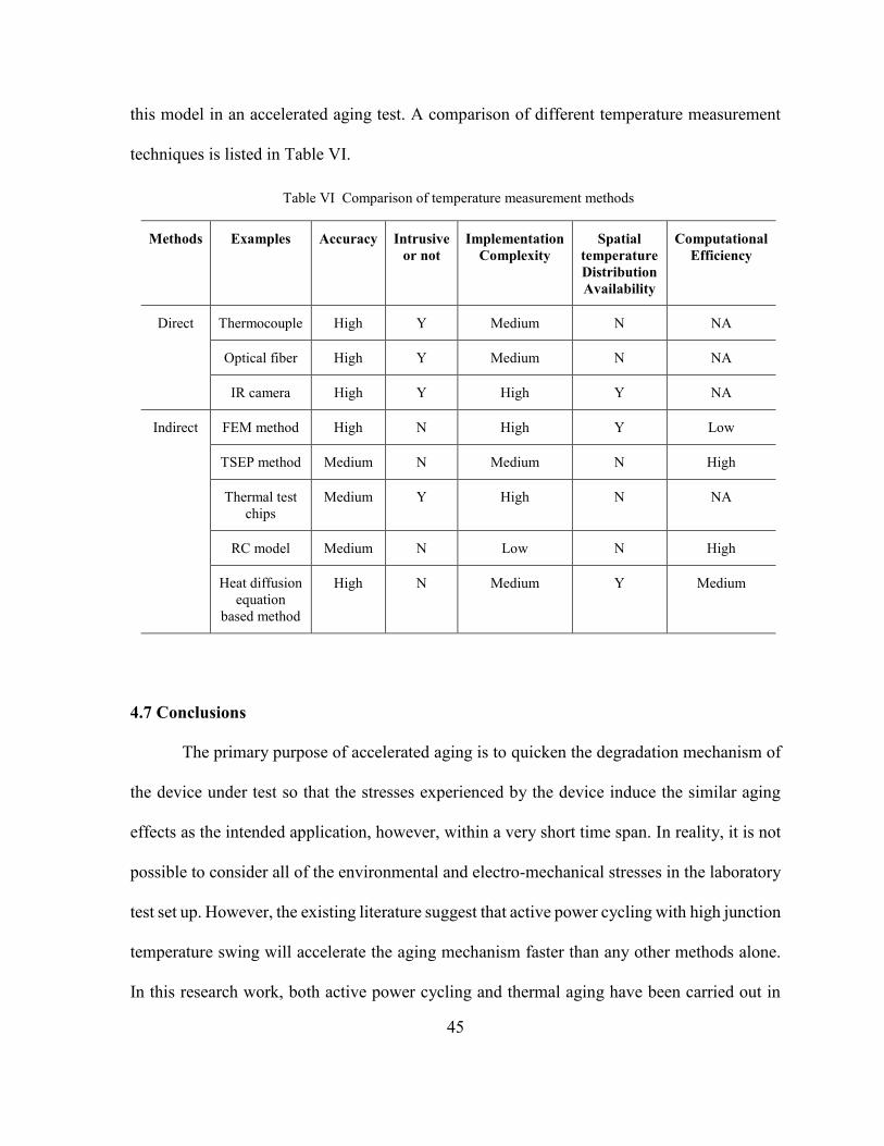
45
this model in an accelerated aging test. A comparison of different temperature measurement
techniques is listed in Table VI.
4.7 Conclusions
The primary purpose of accelerated aging is to quicken the degradation mechanism of
the device under test so that the stresses experienced by the device induce the similar aging
effects as the intended application, however, within a very short time span. In reality, it is not
possible to consider all of the environmental and electro-mechanical stresses in the laboratory
test set up. However, the existing literature suggest that active power cycling with high junction
temperature swing will accelerate the aging mechanism faster than any other methods alone.
In this research work, both active power cycling and thermal aging have been carried out in
Table VI Comparison of temperature measurement methods
Methods Examples Accuracy Intrusive
or not
Implementation
Complexity
Spatial
temperature
Distribution
Availability
Computational
Efficiency
Direct Thermocouple High Y Medium N NA
Optical fiber High Y Medium N NA
IR camera High Y High Y NA
Indirect FEM method High N High Y Low
TSEP method Medium N Medium N High
Thermal test
chips
Medium Y High N NA
RC model Medium N Low N High
Heat diffusion
equation
based method
High N Medium Y Medium

46
order to accelerate the aging of the device. The details of the aging setup and process will be
discussed in the following respective chapters.

47
CHAPTER 5
SSTDR BASED DEGRADATION DETECTION
5.1 Introduction
High thermal and electrical stress, over a period of time tends to deteriorate the health
of power electronic switches. Being a key element in any high-power converter systems, power
switches such as insulated-gate bipolar junction transistor (IGBT) and metal-oxide
semiconductor field-effect transistor (MOSFET) are constantly monitored to predict when and
how they might fail. A huge fraction of research efforts involves the study of power electronic
device reliability and development of novel techniques with higher accuracy in health
estimation of such devices. Until today, no other existing techniques can determine the number
of lifted bond wires and their locations in a live IGBT module, although this information is
extremely helpful to understand the overall state of health (SOH) of an IGBT power module.
Through this research, a novel method for online condition monitoring of IGBTs and IGBT
modules using spread spectrum time domain reflectometry (SSTDR) has been proposed.
Unlike traditional methods, this research work concentrates at the gate terminals (low voltage)
of the device instead of looking at the collector side. In addition, the RL-equivalent circuit to
represent a bond wire has been developed for the device under test and simulated in CST Studio
Suite to measure the reflection amplitudes. Experimental results were obtained using a
prototype reflectometry hardware, and both the simulation and experimental results have been
compared. These results prove that a single measurement is sufficient to predict the failure of
the device instead of looking at the traditional precursor parameter (VCEON). With only two sets
of measurements, it is possible to locate the aged device inside a module and detect the number
of bond wire lift offs associated to that device.

48
5.2 Fundamentals of SSTDR
Several reflectometry methods are currently being used in the field of reliability and
condition monitoring. Among them, SSTDR is the most immune to noise and faces least
interference, which make it an ideal test system for any power converter. The block diagram
of SSTDR prototype hardware is shown in Figure 7 [19].
Traditional time domain reflectometry (TDR) uses a high-amplitude and high-
frequency signal which requires the system to be in offline so that the TDR signal does not
interfere with the system. In addition, TDR requires a wide dynamic range of frequencies to
transmit and to receive the reflected signals. On the other hand, SSTDR sends down a
significantly lower amplitude signal (usually around or below 100mV and lowest could be
22mV) with a frequency of several hundreds of kHz to several MHz making it non-interfering
with the system operation. Unlike traditional TDR, SSTDR method sends a high frequency
sine wave modulated pseudo noise (PN) through the cable. When this signal finds any
impedance mismatch it reflects back. The percentage of reflection depends on the impedance
contrast between the characteristic impedance of its propagation path and the impedance at the
point of mismatch. Then the reflected and incident signal is cross-correlated creating a peak at
Figure 7: Schematic diagram of the SSTDR system showing the setup to characterize an IGBT in a live
converter. [Courtesy: livewire innovation, 2012] [19]

49
the center frequency of the SSTDR. Since the incident signal and noise signals are not
synchronized, their cross correlation yields a flat spectrum. That is why the SSTDR signal is
highly immune to noise and interference. An example field-programmable-gate-array (FPGA)-
based SSTDR evaluation kit W50A0071, which is an R&D product from Livewire Innovation,
has been shown in Figure 8. This hardware works in two modes: (i) static and (ii) intermittent.
In static mode, it requires external triggering for initializing each scan meaning it scans just for
once after the trigger initialization. In contrast, intermittent tests scan the system continuously
to detect short duration impedance change in SSTDR signal propagation path.
SSTDR is traditionally used to detect impedance discontinuity in electric power lines,
and based on the experimental data, SSTDR can be used to detect the presence of cracks and
voids in large IGBT modules by considering the entire module as a multi-conductor complex
transmission line. This method can be made extremely sensitive (to locate small impedance
changes), and extremely precise in both space and time, by using a longer PN code to increase
the effective bandwidth of the system [169] – [171]. In addition, the SSTDR can be routed in
a controlled way by the use of simple filters in the current trace on the PCB, leading to a very
Figure 8: Photograph of the FPGA-based SSTDR hardware (an R&D product from Livewire
Innovation).

50
accurate signal injection method. Like other reflectometry method, SSTDR magnitude or the
reflection coefficient Γ can be expressed as:
Γ = 𝑉𝑟𝑒𝑓𝑙𝑒𝑐𝑡𝑒𝑑
𝑉𝑖𝑛𝑐𝑖𝑑𝑒𝑛𝑡=
𝑍𝐿−𝑍𝑜
𝑍𝐿+𝑍𝑜 (19)
Where, ZO is the characteristic impedance of the line, and ZL is the impedance of the
discontinuity [39].
SSTDR generated data could be potentially used to detect the parametric variations
caused by thermal and electrical stresses in IGBT modules and the results are independent of
the IGBT’s operating points. The DUT is a dual pack module which consists of 6 IGBT
devices, with their corresponding anti-parallel diodes. These devices and diodes are
interconnected with a total of 48 bond wires. Three IGBTs and three diodes are connected in
parallel, forming the top IGBT, and the remaining devices form the bottom IGBT as shown in
Figure 9.
Figure 9: (a) Infineon dual pack IGBT module (FF450R12ME4) without top cover (b) Simplified schematic
of the module

51
Each of the bond wires present in this module has its own resistance and inductance.
The interconnections are made in such a fashion that they can mimic a very complex
transmission line network. When any device ages, the ON-state resistance (RON) value will be
different than that of the healthy device. Similarly, if any bond wire lift-off occurs, the overall
impedance seen from any two terminals will be different than it was before.
Let the equivalent impedance for a healthy module seen from gate and emitter terminals
of the top IGBT device be ZG1E1, H and with aging, this impedance is increased to ZG1E1,A , then
if the change in these two measurement is denoted by ΔZG1E1, we can express this value as
shown in the equation (20) below:
ΔZG1E1 = ZG1E1, H - ZG1E1, A (20)
Now, the reflection coefficientΓ, presented in equation (19), will give the impression
of this difference in impedance, and a non-zero value will illustrate the aging of the module.
5.3 Accelerated Aging and Degradation Detection
5.3.1 Active Power Cycling of IGBT
The DUT, shown in Figure 10, was placed in an accelerated aging station (shown in
Figure 11) to stress it electrically and thermally. The simultaneous stress was achieved by
stopping the coolant flow during the ON-state of the DUT. This active power cycling technique
helps to induce aging in the device in a more efficient way than stressing it either electrically
or thermally. A 600A Lambda-TDK (EMS 7.5-600-2-D-RSTL) power supply was used to push
current through the device, and 313A DC current was supplied between the collector and
emitter terminals during the aging process. The number of cycle was counted based on the
temperature swing of the device. The swing in temperature was 100°C (ΔT) starting from 50°C

52
and ending at 150°C of case temperature. A k-type thermocouple was used to monitor the
temperature.
A Lab-Jack T7-Pro DAQ was utilized to record VCEON, collector current (IC), and case
temperature (TC). Once the temperature reached 150°C, the power supply automatically
stopped sending power to the device and coolant flow was activated.
Figure 10: Infineon IGBT power module (FF450R12ME4) without top cover

53
Similarly, when the device’s case temperature went down to 50°C, the power supply
started pushing current to the collector, and the coolant pump stopped the coolant flow. This
control of the power supply was incorporated by using a power MOSFET in series with the
DUT at the collector side, and this switch was turned ON and OFF in order to activate or
deactivate the power supply. This ensured the full conduction of the device under test. In order
to make the cooling efficient, a heat sink was attached underneath the IGBT module, and
Ethylene-glycol was used as the cooling agent. The overall schematic is presented is Figure
12.
Figure 11: Active power cycling setup

54
5.3.2 Experimental Setup and Test Results
The SSTDR signal was applied at both of the gates of top and bottom IGBT, and
simultaneously the DAQ was recording the VCEON data (plotted and shown in Figure 13).
Figure 14 illustrates the simplified Infineon module and shows the SSTDR test points: G1, E1
(1b), G2, and E2 (2b). This device was aged at two different levels, and data obtained at each
level was compared with the measurements consistent to the zero aged device. Aging level 1
was defined as 400 aging cycles, and aging level 2 was considered once the device failed. The
SSTDR data was recorded for frequencies 3MHz, 12MHz, and 48MHz for collector current
levels of 0A, 25A, and 50A.
From Figure 13, it is apparent that with the aging i.e., as the number of cycles increases,
the VCEON keeps increasing and gives a spike at around 800 cycles as the change is about 5%
Figure 12: Schematic of the accelerated aging station

55
of the initial voltage. At this point the IGBT can be considered as non-functional. This pattern
of IGBT’s VCEON is very common and can be found in many condition monitoring literatures
[172], [173]. Now, according to equation (16), it is expected that when IGBT goes through
aging, the ON-resistance will increase and the auto-correlated amplitude of SSTDR will
produce a lower magnitude. Figure 15 shows the auto-correlated amplitude of SSTDR signal
recorded between the gate and emitter terminals of the top and bottom IGBT respectively. The
zoomed portion within this plot clearly shows that there is a significant difference between the
healthy and aged data. As the level of aging increases i.e., RON increases, the amplitude of the
auto-correlated amplitude keeps falling, which supports the reflectometry theory stated in
equation (19).
Figure 13: VCEON vs number of cycles plot

56
Figure 14: Simplified SSTDR test schematic: TP1 and TP2 represent SSTDR test points for top
and bottom IGBT’s gate-emitter interface respectively
Figure 15: SSTDR auto-correlated amplitude plot
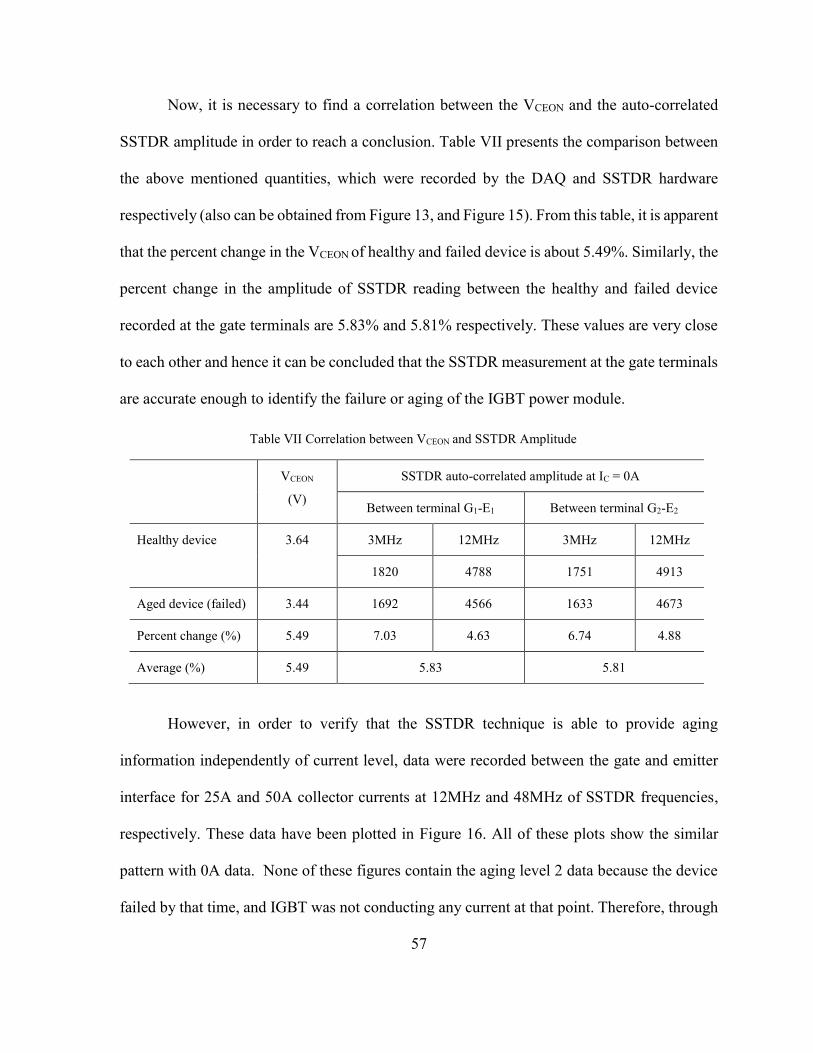
57
Now, it is necessary to find a correlation between the VCEON and the auto-correlated
SSTDR amplitude in order to reach a conclusion. Table VII presents the comparison between
the above mentioned quantities, which were recorded by the DAQ and SSTDR hardware
respectively (also can be obtained from Figure 13, and Figure 15). From this table, it is apparent
that the percent change in the VCEON of healthy and failed device is about 5.49%. Similarly, the
percent change in the amplitude of SSTDR reading between the healthy and failed device
recorded at the gate terminals are 5.83% and 5.81% respectively. These values are very close
to each other and hence it can be concluded that the SSTDR measurement at the gate terminals
are accurate enough to identify the failure or aging of the IGBT power module.
However, in order to verify that the SSTDR technique is able to provide aging
information independently of current level, data were recorded between the gate and emitter
interface for 25A and 50A collector currents at 12MHz and 48MHz of SSTDR frequencies,
respectively. These data have been plotted in Figure 16. All of these plots show the similar
pattern with 0A data. None of these figures contain the aging level 2 data because the device
failed by that time, and IGBT was not conducting any current at that point. Therefore, through
Table VII Correlation between VCEON and SSTDR Amplitude
VCEON
(V)
SSTDR auto-correlated amplitude at IC = 0A
Between terminal G1-E1 Between terminal G2-E2
Healthy device 3.64 3MHz 12MHz 3MHz 12MHz
1820 4788 1751 4913
Aged device (failed) 3.44 1692 4566 1633 4673
Percent change (%) 5.49 7.03 4.63 6.74 4.88
Average (%) 5.49 5.83 5.81

58
these measurements we can conclude that the SSTDR test data does not depend on the current
level of the device, and a single measurement is adequate to identify any aging related
information inside the IGBT power module.
In addition to the monitoring at the gate terminals, SSTDR were applied between the
collector, C1 (1a) and emitter, E2 (2b) interface (nodes are shown in Figure 14) of the IGBT at
different current levels (25A and 50A) and SSTDR frequencies (12MHZ and 48MHz). These
data were plotted in Figure 17 including the zoomed portions to have a better clarity.
Interestingly, these plots show the similar pattern of aging as depicted in previous plots. This
matching information proves that SSTDR based condition monitoring is independent of nodes
and frequency at which the signal is applied. However, it is advantageous to connect to the
gate side for the lower voltage level and ease of access.
Figure 16: SSTDR auto-correlated amplitude plot
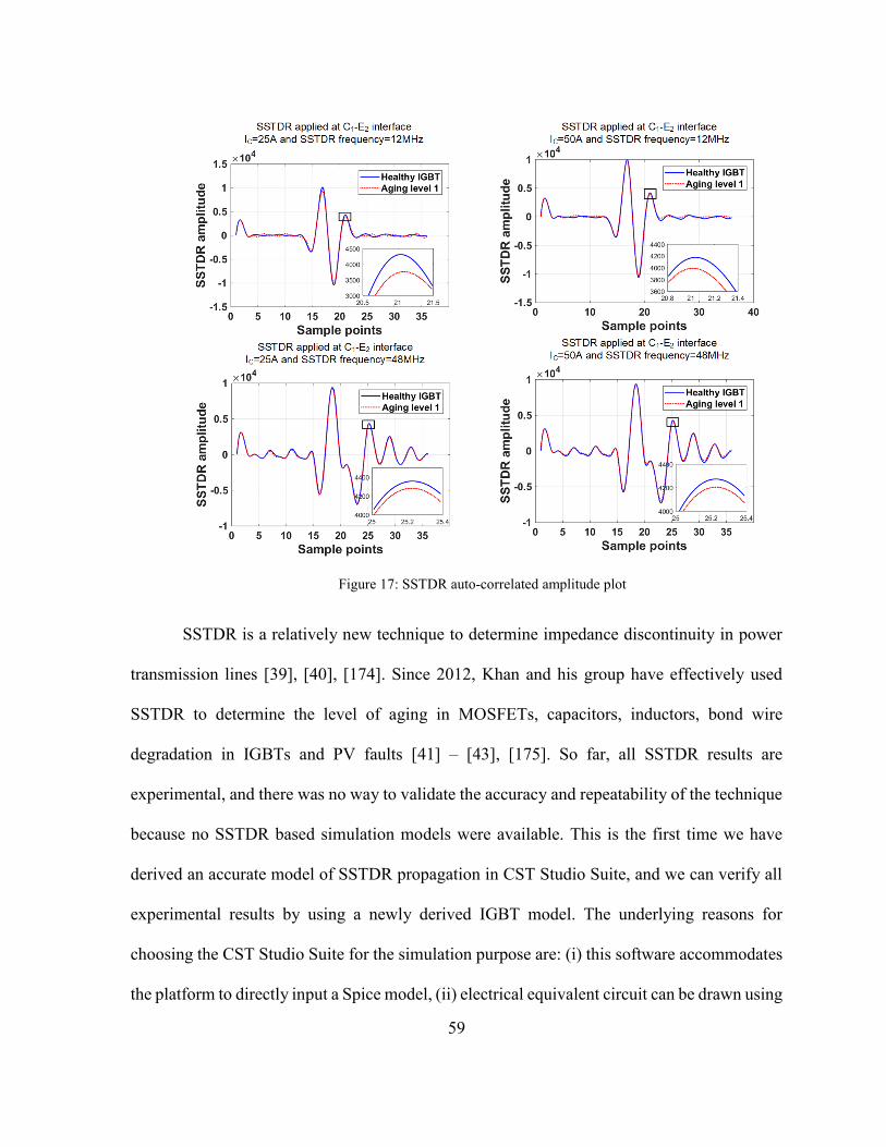
59
SSTDR is a relatively new technique to determine impedance discontinuity in power
transmission lines [39], [40], [174]. Since 2012, Khan and his group have effectively used
SSTDR to determine the level of aging in MOSFETs, capacitors, inductors, bond wire
degradation in IGBTs and PV faults [41] – [43], [175]. So far, all SSTDR results are
experimental, and there was no way to validate the accuracy and repeatability of the technique
because no SSTDR based simulation models were available. This is the first time we have
derived an accurate model of SSTDR propagation in CST Studio Suite, and we can verify all
experimental results by using a newly derived IGBT model. The underlying reasons for
choosing the CST Studio Suite for the simulation purpose are: (i) this software accommodates
the platform to directly input a Spice model, (ii) electrical equivalent circuit can be drawn using
Figure 17: SSTDR auto-correlated amplitude plot

60
its own schematic and component library, (iii) this software is able to measure reflection
parameters at any points of the schematic, and (iv) the SSTDR hardware’s functionality is
based on the reflectometry principle. The following section depicts detail description of the
SSTDR simulation method and results using the CST Studio Suite.
5.4 RL-Equivalent of the Bond Wires in IGBT Module
There are six pairs of IGBTs and diodes in the FF450R12ME4 IGBT power module.
All of them are interconnected via bond wires and each diode and IGBT device are
interconnected with 8 bond wires. The devices in this dual pack module have been numbered
and shown in Figure 9(a). A simplified block diagram is shown in Figure 18.
Since all of the IGBT device and diode pairs are symmetrical and have the exact length
and number of bond wires between them, one pair was modeled in detail, and the remaining
pairs were replicated. After that, the interconnected bond wires between each pair were
modeled in the similar fashion. Multiple bond wires were detached from the module to measure
wire resistance (R), and the measurements were averaged for each bond wire. The length of
Figure 18: Simplified block diagram of FF450R12ME4 dual pack IGBT power module

61
the bond wire was 12mm long, with 2.4mΩ resistance and 12nH inductance. For simplicity,
inductance was estimated as “1mm length equivalent to 1nH inductance” according to [176].
The equivalent circuit of a single pair is shown in Figure 19(a), and Figure 19(b) depicts the
equivalent branch minimized from Figure 19(a).
The bond wire details are explained below:
The collectors of the devices T1 and T2 are connected with 9 bond wires of 7mm
length each, so as the collectors of B1 and B2.
Similarly, the collectors of the devices T2 and T3 are connected with 8 bond wires
of 7mm length each, so as the collectors of B2 and B3.
Figure 19: (a) RL-equivalent of a single pair of IGBT and diode (b) Simplified schematic of a
single pair of IGBT and diode

62
The emitters of B1 and B2 are connected with 8 bond wires of 7mm length, and
the emitters of B2 and B3 are connected with 8 bond wires of 7mm and 3 bond
wires of 10mm length.
Bond wires at the gate and end terminals are connected as stated below:
Gate terminals of T1, T2, and T3 have 3 bond wires of 50mm, 10mm, and 40mm
length respectively. The end points of these bond wires are then connected via a
30mm length bond wire to the external gate terminal, G1.
Similarly, gate terminals of B1, B2, and B3 have 3 bond wires of 45mm, 15mm,
and 45mm length respectively. The end points of these bond wires are then
connected via a 15mm length bond wire to the external gate terminal, G2.
The collector of T1 and emitter of B3 are connected to the external C1 and E2
terminal with 10 parallel bond wires, each of 12mm length.
The emitter of T3 and collector of B1 are connected to the external point E1 and
C2 respectively with 6 parallel bond wires of 14mm length each.
Another bond wire of 21mm length connects the emitter of T3 to the ground
connection of the G1.
The emitter of B2 is connected with the ground of G2 via a 15mm long bond wire.
Incorporating all of the above points into the equivalent circuit, the final bond wire RL-
equivalent circuit will have the schematic shown in Figure 20. The values of the resistors and
inductances have been enlisted in Table VIII.

63
Figure 20: Finalized bond wire RL-equivalent circuit of the IGBT module
Table VIII PARAMETRIC VALUES OF THE ELEMENTS IN RL-EQUIVALENT CIRCUIT OF THE IGBT MODULE
Resistance (mΩ) Inductance (nH)
RT1=RT2=RT3=RB1=RB2=RB3 0.3 LT1=LT2=LT3=LB1=LB2=LB3 1.5
R3,10 0.67 L3,10 3.33
R8,7 0.18 L8,7 0.88
R9,7 0.16 L9,7 0.78
R6,14 0.47 L6,14 2.33
R10,12 0.24 L10,12 1.2
R10 2 L10 10
R15 3 L15 15
R21 4.2 L21 21
R30 6 L30 30
R40 8 L40 40
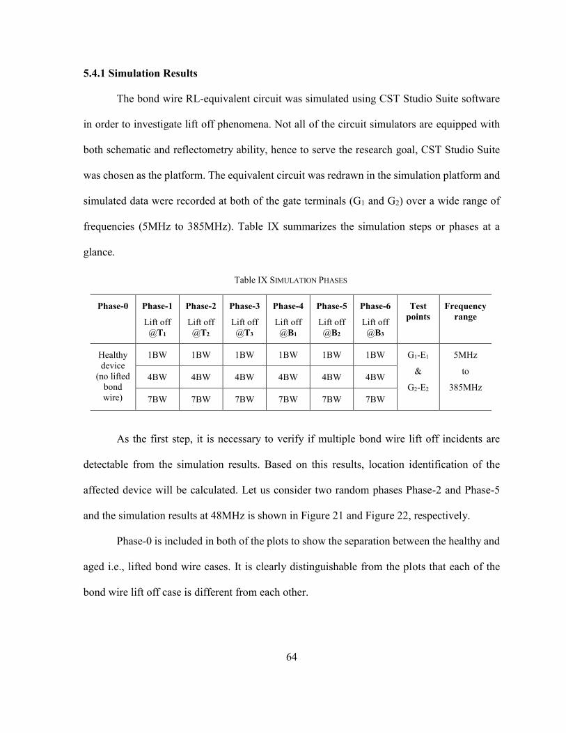
64
5.4.1 Simulation Results
The bond wire RL-equivalent circuit was simulated using CST Studio Suite software
in order to investigate lift off phenomena. Not all of the circuit simulators are equipped with
both schematic and reflectometry ability, hence to serve the research goal, CST Studio Suite
was chosen as the platform. The equivalent circuit was redrawn in the simulation platform and
simulated data were recorded at both of the gate terminals (G1 and G2) over a wide range of
frequencies (5MHz to 385MHz). Table IX summarizes the simulation steps or phases at a
glance.
As the first step, it is necessary to verify if multiple bond wire lift off incidents are
detectable from the simulation results. Based on this results, location identification of the
affected device will be calculated. Let us consider two random phases Phase-2 and Phase-5
and the simulation results at 48MHz is shown in Figure 21 and Figure 22, respectively.
Phase-0 is included in both of the plots to show the separation between the healthy and
aged i.e., lifted bond wire cases. It is clearly distinguishable from the plots that each of the
bond wire lift off case is different from each other.
Table IX SIMULATION PHASES
Phase-0 Phase-1
Lift off
@T1
Phase-2
Lift off
@T2
Phase-3
Lift off
@T3
Phase-4
Lift off
@B1
Phase-5
Lift off
@B2
Phase-6
Lift off
@B3
Test
points
Frequency
range
Healthy
device
(no lifted
bond
wire)
1BW 1BW 1BW 1BW 1BW 1BW G1-E1
&
G2-E2
5MHz
to
385MHz 4BW 4BW 4BW 4BW 4BW 4BW
7BW 7BW 7BW 7BW 7BW 7BW

65
Since the device T2 is closer to the gate G1, hence the magnitude is higher than the
magnitude recorded at G2-E2 interface. Similarly, B2 has a higher magnitude when recorded at
the G2 gate terminal. It is also noteworthy that the values in the y-axis are the absolute
magnitude, whereas, they all are actually negative numbers. So, the true amplitude of the
reflection is decreasing with increasing number of bond wires, which is consistent with
equation (16) as well as with the experimental SSTDR data. In addition, the SSTDR hardware
is a prototype device manufactured by LiveWire Innovation, therefore, the peaks in simulation
Figure 21: Reflection magnitude vs frequency plot when T2 has lifted bond wire (a) recorded at G1-E1
interface (b) recorded at G2-E2 interface
Figure 22: Reflection magnitude vs frequency plot when B2 has lifted bond wire (a) recorded at G1-E1
interface (b) recorded at G2-E2 interface
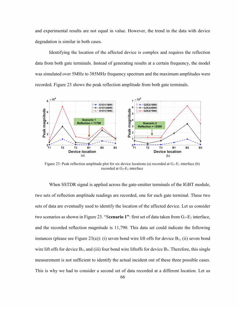
66
and experimental results are not equal in value. However, the trend in the data with device
degradation is similar in both cases.
Identifying the location of the affected device is complex and requires the reflection
data from both gate terminals. Instead of generating results at a certain frequency, the model
was simulated over 5MHz to 385MHz frequency spectrum and the maximum amplitudes were
recorded. Figure 23 shows the peak reflection amplitude from both gate terminals.
When SSTDR signal is applied across the gate-emitter terminals of the IGBT module,
two sets of reflection amplitude readings are recorded, one for each gate terminal. These two
sets of data are eventually used to identify the location of the affected device. Let us consider
two scenarios as shown in Figure 23. “Scenario 1”: first set of data taken from G1-E1 interface,
and the recorded reflection magnitude is 11,790. This data set could indicate the following
instances (please see Figure 23(a)): (i) seven bond wire lift offs for device B1, (ii) seven bond
wire lift offs for device B3, and (iii) four bond wire liftoffs for device B3. Therefore, this single
measurement is not sufficient to identify the actual incident out of these three possible cases.
This is why we had to consider a second set of data recorded at a different location. Let us
Figure 23: Peak reflection amplitude plot for six device locations (a) recorded at G1-E1 interface (b)
recorded at G2-E2 interface
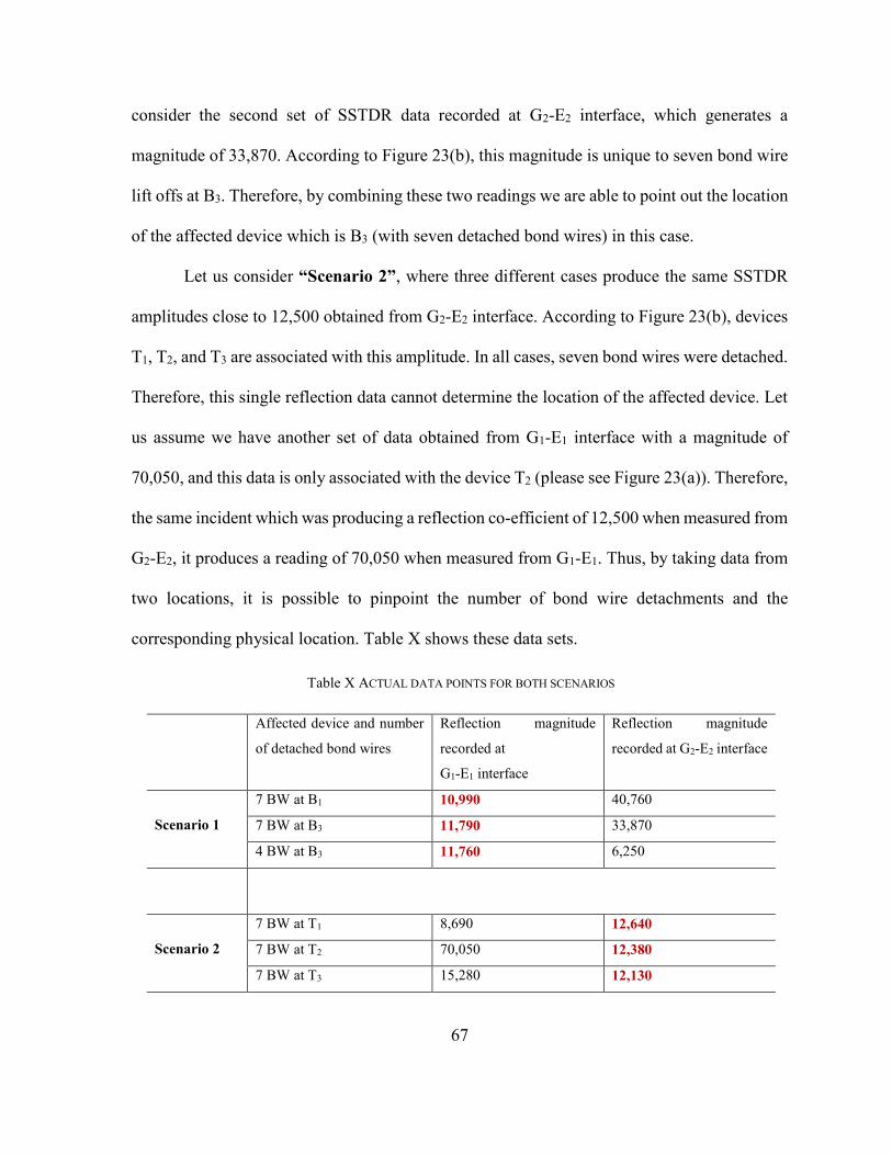
67
consider the second set of SSTDR data recorded at G2-E2 interface, which generates a
magnitude of 33,870. According to Figure 23(b), this magnitude is unique to seven bond wire
lift offs at B3. Therefore, by combining these two readings we are able to point out the location
of the affected device which is B3 (with seven detached bond wires) in this case.
Let us consider “Scenario 2”, where three different cases produce the same SSTDR
amplitudes close to 12,500 obtained from G2-E2 interface. According to Figure 23(b), devices
T1, T2, and T3 are associated with this amplitude. In all cases, seven bond wires were detached.
Therefore, this single reflection data cannot determine the location of the affected device. Let
us assume we have another set of data obtained from G1-E1 interface with a magnitude of
70,050, and this data is only associated with the device T2 (please see Figure 23(a)). Therefore,
the same incident which was producing a reflection co-efficient of 12,500 when measured from
G2-E2, it produces a reading of 70,050 when measured from G1-E1. Thus, by taking data from
two locations, it is possible to pinpoint the number of bond wire detachments and the
corresponding physical location. Table X shows these data sets.
Table X ACTUAL DATA POINTS FOR BOTH SCENARIOS
Affected device and number
of detached bond wires
Reflection magnitude
recorded at
G1-E1 interface
Reflection magnitude
recorded at G2-E2 interface
Scenario 1
7 BW at B1 10,990 40,760
7 BW at B3 11,790 33,870
4 BW at B3 11,760 6,250
Scenario 2
7 BW at T1 8,690 12,640
7 BW at T2 70,050 12,380
7 BW at T3 15,280 12,130

68
5.4.2 Simulation vs Experimental Results
Initial testing was conducted with FF450R12ME4 IGBT modules. These are
EconoDUAL™3 modules with Trench/Fieldstop IGBT4 and Emitter Controlled HE diode,
manufactured by Infineon Technologies. The high power density of this particular module has
made it useful in several commercial, construction, and agricultural vehicle applications where
extended reliability is a key. Each FF450R12ME4 has one top and one bottom IGBT and their
corresponding free-wheeling diodes.
In order to mimic the bond wire lift off, we have intentionally detached the bond wires
in a sequential manner and then observed the SSTDR output. We found this is the only
controlled way to emulate a specific number of bond wire detachment, and the number of
disconnected bond wires cannot be guaranteed using the accelerated aging techniques. This
arrangement is shown in Figure 24(a), and the actual IGBT package is shown in Figure 24(b).
The top IGBT’s collector terminal was connected to the silicon die through 24 bond wires. The
Top IGBT (shown in Figure 9) consists of three IGBT devices connected in parallel, and each
of them has 8 bond wires, and 3 diodes are connected in anti-parallel fashion. Thus, the Top
IGBT has total of 24 bond wires. Figure 24(c) shows the close-up view of the IGBT module.
Similarly, the bottom IGBT has another 3 parallel IGBT devices with a total of 24 bond wires,
and three anti-parallel diodes. The total current through the entire IGBT module is shared
among these 48 bond wires. Therefore, any lift-off associated to any of these wires will lead
to increase in current path resistance and will inhibit natural current flow to the IGBTs. The
main task was to investigate if the SSTDR data could detect these lift-off events once we
sequentially disconnected these wires.

69
The protective gel layer in the IGBT module was removed prior to the testing in order
to get easier access to the bond wires. The module was submerged in the Digesil NC Xtra
solution (a polymer remover) until the gel layer was completely removed. Isolated +15 V DC
voltages were applied across the gate and emitter of both the top and bottom IGBT modules.
SSTDR data were recorded for seven instances (6, 12, 18, 24, 30, 36, and 42 lifted bond wires)
at SSTDR center frequency of 12MHz and 48MHz. The peak amplitudes were compared with
the corresponding peak amplitudes obtained from the simulation. Figure 25 shows the
comparable results at 12MHz, and Figure 26 represents the result obtained at 48MHz, and the
simulation and experimental data are in very close agreement. These figures also show that
when the module have 24 lifted bond wires, the magnitude is the minimum. The experiments
and simulations were conducted for multiple times in multiple modules, and all of the results
showed similar pattern. The reason behind this is yet unknown, however, future research will
address this phenomenon and find out the underlying reason behind it. Since both results
correspond to each other and are repeatable, it is apparent that the location and number of lifted
bond wires can be identified if the results from the both gate terminals are compared.
Figure 24: (a) The actual test setup (b) Photograph of the actual IGBT module used with and without top
cover (c) Close-up view of the IGBT bond wires.
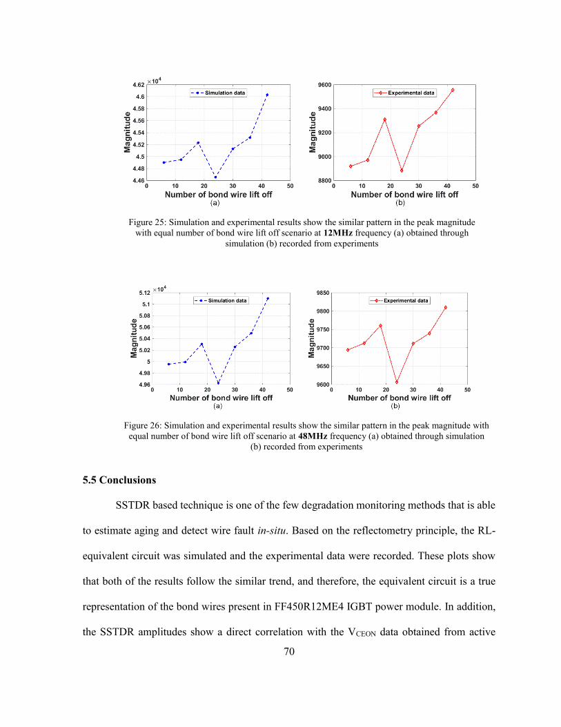
70
5.5 Conclusions
SSTDR based technique is one of the few degradation monitoring methods that is able
to estimate aging and detect wire fault in-situ. Based on the reflectometry principle, the RL-
equivalent circuit was simulated and the experimental data were recorded. These plots show
that both of the results follow the similar trend, and therefore, the equivalent circuit is a true
representation of the bond wires present in FF450R12ME4 IGBT power module. In addition,
the SSTDR amplitudes show a direct correlation with the VCEON data obtained from active
Figure 25: Simulation and experimental results show the similar pattern in the peak magnitude
with equal number of bond wire lift off scenario at 12MHz frequency (a) obtained through
simulation (b) recorded from experiments
Figure 26: Simulation and experimental results show the similar pattern in the peak magnitude with
equal number of bond wire lift off scenario at 48MHz frequency (a) obtained through simulation
(b) recorded from experiments

71
power cycling. Thus, it is possible to determine the location of the lifted BW. The research
outcome documented in this manuscript shows that the total number of BW liftoffs technique
can be extremely helpful in the field applications where the collector-emitter nodes are not
easily accessible due in high voltage applications. This method can also be extended to any
converter circuit topology provided that the data are collected from the gate terminals of every
module which is very feasible. Unlike collector terminal, the gate terminal is always at the
lower potential level which significantly helps in the design phase of any condition monitoring
hardware. Since electrical parameter measurement is not required, this technique not only
reduces the measurement error but also helps in designing the SSTDR hardware at a much
lower rating. Even with proper scaling the hardware can be incorporated in the gate driver
board which will allow the system to be monitored autonomously.
72
CHAPTER 6
ULTRASOUND BASED DEGRADATION DETECTION
6.1 Introduction
Among non-destructive evaluations, ultrasound based tests have become popular in
recent times. The application of ultrasound based crack-detection on large objects are well
explored area. However, their potential in degradation detection of high power
IGBT/MOSFET modules has not yet been utilized. Existing ultrasound based crack or void
detection techniques are either too expensive and/or requires a fluid couplant to submerge the
DUT/structure to be tested [44]. Confocal scanning acoustic microscopy (CSAM) based state-
of-health identification is very popular in a semiconductor die and die-attach between the
copper layer and substrate [45] - [47]. However, this technique cannot be used in a live circuit
for package level degradation detection due to the size and medium constraint of the CSAM
setup (requires the wafer to be submerged in water). In addition, it takes a long time to scan
the device under test compared to any other existing condition monitoring method.
Electromagnetic acoustic transducers (EMATs) does not require any couplant, however, they
require high current injections for testing, and their efficiency is not as effective as the piezo-
electric transducers [48]. In addition, the spread spectrum ultrasound technique requires highly
precise transducer and couplant control to generate reasonably reliable results, and this
technique has only been applied to large structures such as steel blocks [49] - [50]. In this
research work, we have proposed a novel method based ultrasound resonators which is able to
detect bond wire related aging in IGBT power modules. Although, the testing were conducted
in IGBT modules, the method is equally applicable in power MOSFETs as well as in power
converters/inverters.

73
The proposed ultrasound-based technique has the following advantages over existing
methods:
i. Ultrasound resonator based method is able to detect bond wire lift off related
aging in-situ, and irrespective of the operating condition of the module or converter.
ii. Unlike other ultrasound based methods, it does not require any liquid couplant,
and gathers data instantly and continuously.
iii. This method significantly reduces the overall cost compared to the other
condition monitoring methods where additional sensors are required to measure
precursor parameters.
iv. This method can be integrated with the gate driver module if properly scaled.
Therefore, it is expected that the successful implementation of this technique will create
a seminal impact in estimating remaining life especially for IGBTs.
6.2 Ultrasound Fundamentals and Sympathetic String Theory
6.2.1 Ultrasound resonator – a new way of testing electronics live
Ultrasound is one of the most common applications of non-destructive evaluation
(NDE) method for crack detection and characterization in material structures [177]. This
acoustic-ultrasound technique can also be used to find internal surface defects and
discontinuities in power switching devices where cracks and voids along with bond wire lift-
offs are formed due to package related failures. This non-destructive testing technique is based
on the determination of acoustic transmission and reflection at the boundary of two materials
having different acoustic impedances. In view of this fact, ultrasonic waves are also transmitted
and reflected at the junction interface between materials with different acoustic impedances

74
that are formed due to deformation of materials in the device package such as cracks and voids
formation due to delamination in the die-solder layer interface, bond wire lift-off and heel
crack or aluminum metallization reconstruction. The amount of energy that is transmitted or
reflected depends on the contrast in acoustic impedance (Z). The greater the impedance
mismatch, the higher the percentage of energy that will be reflected at the interface or boundary
between one medium and another. If the acoustic impedances of two medium is said to be Z1
and Z2 then the following equation can be used to express the reflection coefficient (R) [178]:
𝑅 = (𝑍2−𝑍1
𝑍2+𝑍1)2
(21)
The relationship between the spectral amplitude of the signal backscattered by an
interface of two mediums and the acoustic impedances of these mediums is expressed below
in equation (22) [178].
𝐴𝑟 = 𝐾𝑟𝑍2−𝑍1
𝑍2+𝑍1 (22)
Also, the spectral amplitude of the transmitted acoustic signal is shown in equation (23)
[179].
𝐴𝑡 = 𝐾𝑡𝑍2
𝑍2+𝑍1 (23)
Where, Ar= spectral amplitude of the reflected signal, At = spectral amplitude of the
transmitted signal, Z1= acoustic impedance of the first medium, Z2 = acoustic impedance of
the second medium, Kr, Kt= constants which depend on the transfer functions of the acoustic
signal paths. For an IGBT module (for example, we used FF450R12ME4) the bond wires are
encapsulated in a silicone gel layer to prevent moistures to come in contact with the die.
Therefore, a contrast in acoustic impedance exists between the gel layers (Z2) and the bond
wires (Z1). Once there is a crack or lift off associated with these bond wires, the spectral

75
amplitude of the reflected wave will be different than the corresponding amplitude for a healthy
module. Using this phenomenon, the bond wire lift off related device degradation can be
identified using the ultrasound resonators.
Ultrasonic transducers or ultrasonic resonators are a type of acoustic sensor that can be
used as both transmitter and receiver. As shown in Figure 27, if this ultrasonic transducer can
be mounted in such a way that the transmitted ultrasonic beam can be impinged on a surface
crack and voids in a solid at an incident angle of θ, the emitted energy distribution will be the
result of contribution from two components [177]. The first component (D) is the diffraction
of a ray at the tip of the crack creating a spherical wave front from the mode conversion, and
the second one (R) is the wave reflected from the mouth of the surface crack. The location and
the depth (d) of the surface crack or void can be determined as follows:
𝑑 =𝛥𝑙
2𝑐𝑜𝑠θ=
V𝛥𝑡
2𝑐𝑜𝑠θ (24)
Where, V denote the velocity of the incident wave; ∆t is the difference of the arrival
times and ∆l is the path difference between these two wave components. It is important to note
that based on the incident angle (θ), depth and location of the surface defects, the position of
the receiver sensor needs to be adjusted to capture the reflected signal components of
maximum energy. Considering this fact, the optimized number of sensors along with their
optimum locations are needed for each IGBT chip to determine their corresponding surface
defects.

76
6.2.2 Sympathetic resonance in acoustic string instrument
Sympathetic resonance or vibration can be defined as “resonant or near-resonant
response of a mechanical or acoustical system excited by energy from an adjoining system in
steady-state vibration” [180]. Several musical instruments use the sympathetic resonance in
order to produce characteristic sounds. These instruments include but are not limited to Sitar
(shown in Figure 28(a)), Sarangi, Viola D’amore, Baryton, Sarod, Ukelin, and so on [181].
The basic principle is to excite one string of any of these instruments, and other strings will
resonate at their either fundamental or harmonic frequencies. The strings of such musical
instruments are usually connected to a vibrating body, known as the soundboard. This
soundboard is made of multiple materials with compound shapes. This helps in generating
efficient sound propagation. Thus, creating an effective coupling between the soundboard and
the strings, it is possible to vibrate one string if another string is excited. This phenomenon is
referred as the sympathetic resonance [180].
The sympathetic resonance is not only important in musical applications but also plays
a vital role in the field applications of electric machineries. For example, if two or more motors
Figure 27: Interaction of an ultrasonic shear wave from a surface crack

77
are installed on the same base, then the vibration energy may transfer to the nearby
motor/machine and may damage the machine even if it is in standby mode. This will only occur
if the vibrating frequency of the running machine matches the resonance frequency of the
nearby motor, which in other word is due to the sympathetic resonance [182]. So, the vibration
signature, both the frequency and amplitude, is useful in fault diagnosis of the electric motors.
Another application of sympathetic resonance can be found in [183], where the authors have
measured the Young's modulus of biological electret-bone.
Ultrasonic based bond wire welding has become very popular in recent times due to its
higher reliability compared to tradition soldering techniques [184]. However, to detect the
bond wire related degradation using ultrasound resonators, the first and foremost task is to find
out the resonant frequency of the bond wires present in the IGBT module. Authors in [185] –
[186] have worked on establishing a relationship between the resonant frequency and the
length of the bond wire. In order to create a damage in a bond wire two things play important
role depending on the length of the bond wires; resonant frequency and the magnitude of
resonance. Following two equations can be referred to explain this relationship [185]:
ωr = 𝑘1𝑑
𝑙2 (25)
ar = 𝑘2𝑙4 (26)
Where, ωr = resonant frequency = 2πfr, k1 = constant based on bond wire material, d =
diameter of the bond wire, l = length of the bond wire, ar = resonant amplitude, k2
= constant based on bond wire material.
According to these two above mentioned equations, a longer wire requires a lower
resonant frequency (f ∝ 1
𝑙2 ) but a higher magnitude (a ∝ 𝑙4). Fortunately, all of the 48 bond
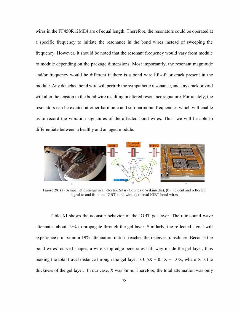
78
wires in the FF450R12ME4 are of equal length. Therefore, the resonators could be operated at
a specific frequency to initiate the resonance in the bond wires instead of sweeping the
frequency. However, it should be noted that the resonant frequency would vary from module
to module depending on the package dimensions. Most importantly, the resonant magnitude
and/or frequency would be different if there is a bond wire lift-off or crack present in the
module. Any detached bond wire will perturb the sympathetic resonance, and any crack or void
will alter the tension in the bond wire resulting in altered resonance signature. Fortunately, the
resonators can be excited at other harmonic and sub-harmonic frequencies which will enable
us to record the vibration signatures of the affected bond wires. Thus, we will be able to
differentiate between a healthy and an aged module.
Table XI shows the acoustic behavior of the IGBT gel layer. The ultrasound wave
attenuates about 19% to propagate through the gel layer. Similarly, the reflected signal will
experience a maximum 19% attenuation until it reaches the receiver transducer. Because the
bond wires’ curved shapes, a wire’s top edge penetrates half way inside the gel layer, thus
making the total travel distance through the gel layer is 0.5X + 0.5X = 1.0X, where X is the
thickness of the gel layer. In our case, X was 8mm. Therefore, the total attenuation was only
Figure 28: (a) Sympathetic strings in an electric Sitar (Courtesy: Wikimedia), (b) incident and reflected
signal to and from the IGBT bond wire, (c) actual IGBT bond wires

79
6.93dB, and the input energy from the ultrasound sensors are sufficient to interact with the
bond wires and to reflect back to the receiver sensors. Figure 28(b) shows several interactions
between the acoustic wave and a bond wire including few possible reflection paths.
6.3 Analytical Model of Ultrasound Wave Propagation in IGBT Module
6.3.1 Modes of sound wave propagation:
Multiple atoms constitute a material and each material may be subjected to oscillatory
motion about their steady state positions if an external vibrational force is applied. However,
this oscillatory behavior can arise only if the material or the medium is stressed within its
elastic limit. The electrostatic restoration force between the particles of the medium combines
with the inertia of the particles and leads to the oscillatory motion of the medium. Based on
the characteristics of this oscillation, sound wave can travel through a medium in four major
modes namely, (i) longitudinal waves (ii) shear waves (iii) surface waves and (iv) plate waves.
In ultrasound based testing, longitudinal and shear waves are most commonly utilized modes
of sound propagation [187]. It is important to know how these two waves are propagated
through a medium. Figure 29 illustrates the particle movements related to the longitudinal and
shear waves.
Table XI ACOUSTIC BEHAVIOR OF THE GEL LAYER INSIDE FFF450R12ME4 DUAL PACK IGBT MODULE
Density
of
silicone
gel (ρ)
Kgm-3
Acoustic
Velocity
in gel
layer(ν)
ms-1
Acoustic
impedance of
gel layer
(Z=ρν)
MRayls
Attenuatio
n
coefficient
in gel layer
(∝) dBcm-
1
Output power
of the
resonator at
100mvp-p
input voltage
(A0 =10log𝐼
𝐼0)
dB
Thickness
of the gel
layer (t)
cm
Attenuated
amplitude
(A(z)=A0
𝑒−∝𝑍
8.7 )
Total
attenuati
on
(dB)
700 1490 1.043 2.175 36.81 0.8 29.88 6.93
(18.82%)
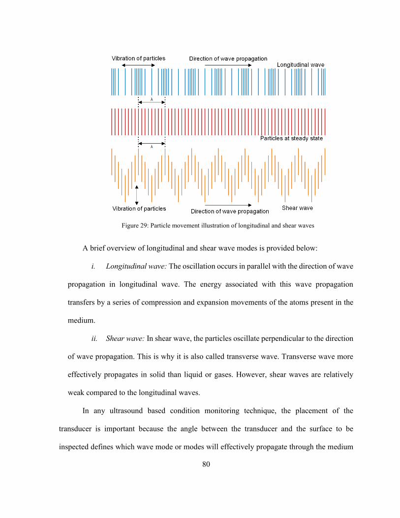
80
A brief overview of longitudinal and shear wave modes is provided below:
i. Longitudinal wave: The oscillation occurs in parallel with the direction of wave
propagation in longitudinal wave. The energy associated with this wave propagation
transfers by a series of compression and expansion movements of the atoms present in the
medium.
ii. Shear wave: In shear wave, the particles oscillate perpendicular to the direction
of wave propagation. This is why it is also called transverse wave. Transverse wave more
effectively propagates in solid than liquid or gases. However, shear waves are relatively
weak compared to the longitudinal waves.
In any ultrasound based condition monitoring technique, the placement of the
transducer is important because the angle between the transducer and the surface to be
inspected defines which wave mode or modes will effectively propagate through the medium
Figure 29: Particle movement illustration of longitudinal and shear waves

81
and/or reflect from the surface under inspection. This angle is defined as the critical angle.
There are three critical angles related to the ultrasound wave propagation: first, second, and
third critical angles [188]. Figure 30 shows these angles where θ1 represents first critical angle,
θ2 represents second critical angle, and θ3 is defined as the third critical angle.
Following scenarios explain the relative relations between the incident angles and the
wave modes:
Scenario-1: When the sound wave intersects the surface under inspection at an angle
of θ =0°, it only reflects or refracts longitudinal waves, there will be no shear wave in either of
the mediums.
Scenario-2: If the angle of incident is between 0 and θ1, (0< θ< θ1) both longitudinal
and shear waves will reflect and travel into the second medium.
Scenario-3: When θ1< θ< θ2, longitudinal wave does not penetrate into the second
medium, only shear wave is refracted into the second medium. However, both of these waves
are reflected into the first medium from incident point of the medium interface.
Figure 30: Critical angles for an incident ultrasound wave

82
Scenario-4: When θ2< θ< θ3, none of the waves penetrate into the second medium and
both of the longitudinal and shear waves reflects back from the surface of incident into the first
medium.
Scenario-5: When θ ≥ θ3, longitudinal waves disappear and only shear waves reflect
back into the first medium.
Therefore, the location of the ultrasound transducers and receivers are highly important
in order to detect the reflected wave mode coming from the medium interface.
6.3.2 Frequency, wavelength, and defect detection:
In non-destructive testing (NDT) such as ultrasound based defect detection is highly
dependent on the ultrasound frequency and the wavelength of the propagating sound wave
[189]. The detection ability in an ultrasound based technique is inversely proportional to the
wavelength of the sound wave- shorter the wavelength, higher the chances of detecting smaller
discontinuity i.e., better the sensitivity. The relationship between the frequency, wavelength,
and velocity of the sound wave in a medium can be described by the following equation:
𝜆 =𝑉
𝑓 (27)
Here, λ is the wavelength of sound wave, f is the frequency, and V represents the
velocity of the sound wave in the medium. Since the velocity is constant in a uniform medium,
higher the frequency of the sound wave shorter the wavelength will be. Therefore, smaller
surface defects, voids, bond wire lift-offs and heel cracks are more likely to be detected when
the frequency is higher. It is important to note that, the discontinuity should be at least one-
half wavelength long for a successful and repetitive detection [190]. Resolution is important
as well since it defines the ability of the system to detect discontinuities that are close to each
other. Resolution of the ultrasound technique is also directly proportional to the frequency of

83
the propagating sound wave i.e., shorter the wavelength higher the resolution [191]. However,
selection of a very high frequency sound wave may undesirably affect the condition monitoring
system. If the surface to be inspected or the material has a very high grain size and the
frequency is very high, then it is possible that the spacing of the large grained surfaces may be
considered as the discontinuity while conducting the ultrasound test. Therefore, it is important
to know about the material to be tested and accordingly choose the frequency of the
piezoelectric crystal. It is also to be remembered that the penetration depth of the sound wave
is inversely proportional to the frequency, and therefore, the frequency selection is the most
important criterion in ultrasound based defect detection.
Another important parameter in ultrasound based defect detection is the acoustic
impedance of the medium. It is clear from equation (21) and equation (22) that higher the
impedance contrast between the mediums, greater the reflection occurs. The relation between
the acoustic impedance and the velocity of the sound wave can be expressed by the equation
below [192]:
Z=ρV (28)
Here, Z is the acoustic impedance, ρ is the density of the medium, and V represents
the velocity of sound through the medium. It is apparent that the velocity of sound varies from
one medium to another because the density and elastic constant is different for different
materials. Following equation shows the mutual relationship between these three parameters:
𝑉 = √𝐸
𝜌 (29)

84
Where, V is the velocity of the sound, E is the elastic constant (Young’s modulus) of
the medium, and ρ is the density of the medium.
6.3.3 Attenuation of ultrasound wave
Attenuation in the sound wave occurs due to the scattering and absorption in the
medium. As a result, the intensity of the ultrasound wave reduces with distance as the wave
propagates through any material. Therefore, attenuation is an important parameter in
ultrasound based non-destructive evaluation (NDE). Following equation expresses the mutual
relationship between the attenuation constant of a medium and the amplitude of the attenuating
sound wave:
𝐴 = 𝐴0𝑒−µ𝐴𝑥 (30)
Here, A0 is the un-attenuated amplitude of the sound wave, A is the attenuated
amplitude at a distance x in the direction of wave propagation, and µA is the attenuation factor.
The attenuation coefficient (α) can be experimentally measured using the following equation
[192] - [193]:
𝛼 =−20
2(𝑗−𝑖)𝑑 log
𝐴𝑗
𝐴𝑖 (31)
Where, Ai and Aj are the amplitude of the ith and jth echoes and d is the distance travelled
by the ultrasound wave.
Now, the attenuation coefficient, α, can be expressed in terms of µA since 20 log (A/A0)
represents the amplitude reduction in decibel (dB), and therefore,
α=20 * log (e) * µA = 8.7µA (32)
If we replace µA from equation (32) into equation (30), we get that the attenuated
amplitude of the propagating ultrasound wave is,
85
𝐴 = 𝐴0𝑒−𝛼𝑥
8.7 (33)
Later in this section, equation (33) will be useful in deducing the ultrasound wave
amplitude received by the piezoelectric sensors.
6.3.4 Snell’s Law, wave equation, and reflection amplitudes
A dual pack IGBT module manufactured by Infineon has been chosen as the device
under test (DUT). This module (FF450R12ME4) has 6 IGBT devices and 6 corresponding
freewheeling diodes. These diodes and IGBT devices are connected via bond wires. A silicone
gel is used to seal off these bond wires and devices. When piezoelectric crystals are used to
apply ultrasound signal, the elastic wave produced from these resonators can propagate through
the gel layer in the form of compressional (longitudinal) and transverse (shear) waves
depending on the angle of incident. Figure 31 shows the reflection and refraction phenomena
at the medium interface when the sound wave has an oblique incident angle and the density of
two media are different i.e., the acoustic impedances are distinct.
According to Snell’s law:
sinθLI
VL1=
sinθLR
VL2=
sinθTI
VT1=
sinθTR
VT2 (34)
Now, consider the gel layer has the density ρ, the displacement potentials
corresponding to compressional and transverse velocities are Φ and Ψ respectively, and then
the ultrasound wave can be characterized using the well-known elastic wave equation as shown
below [194]:
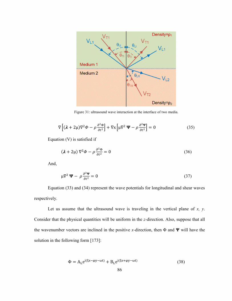
86
∇ [(𝝀 + 2µ)∇2𝛷 − 𝜌𝜕2Φ
𝜕𝑡2] + ∇x [µ∇2𝚿 − 𝜌
𝜕2𝚿
𝜕𝑡2] = 0 (35)
Equation (V) is satisfied if
(𝝀 + 2µ)∇2𝛷 − 𝜌𝜕2Φ
𝜕𝑡2= 0 (36)
And,
µ∇2𝚿 − 𝜌𝜕2𝚿
𝜕𝑡2= 0 (37)
Equation (33) and (34) represent the wave potentials for longitudinal and shear waves
respectively.
Let us assume that the ultrasound wave is traveling in the vertical plane of x, y.
Consider that the physical quantities will be uniform in the z-direction. Also, suppose that all
the wavenumber vectors are inclined in the positive x-direction, then Φ and Ψ will have the
solution in the following form [173]:
Φ = ALei(ξx−φy−ωt) + BLe
i(ξx+φy−ωt) (38)
Figure 31: ultrasound wave interaction at the interface of two media.
87
𝚿 = ATei(ζx−βy−ωt) + BTe
i(ζx+βy−ωt) (39)
Where, AL, AT are incident longitudinal and transverse wave amplitudes respectively.
BL and BT are reflected longitudinal and transverse wave amplitudes respectively. Also, ξ and
φ are the wavenumber component of the longitudinal wave with the polar
coordinate(𝑘𝐿 sin 𝜃𝐿 , 𝑘𝐿 cos 𝜃𝐿). Similarly, ζ and β are the wavenumber component of the
transverse wave with the polar coordinate(𝑘𝑇 sin 𝜃𝑇 , 𝑘𝑇 cos 𝜃𝑇). The relationship between
the reflection and incident amplitudes can be expressed as shown in below [195]:
[BLBT] = [
SLL STLSLT STT
][ALAT] (40)
Here, 𝐒(𝜃𝐿 , 𝜃𝑇) = [SLL STLSLT STT
] represents the scattering matrix and the subscripts
represent the incident and reflected waves. Such as SLT represents the reflected transverse wave
due to incident longitudinal wave of unit amplitude. Expressions for the index terms in
S(𝜃𝐿 , 𝜃𝑇) are shown below:
SLL =sin2𝜃𝐿 sin 2𝜃𝑇−𝑘
2𝑐𝑜𝑠22𝜃𝑇
sin2𝜃𝐿 sin 2𝜃𝑇+𝑘2𝑐𝑜𝑠22𝜃𝑇 (41)
STL =−2𝑘2 sin2𝜃𝑇 cos2𝜃𝑇
sin2𝜃𝐿 sin 2𝜃𝑇+𝑘2𝑐𝑜𝑠22𝜃𝑇 (42)
SLT =2 sin2𝜃𝐿 cos2𝜃𝑇
sin2𝜃𝐿 sin 2𝜃𝑇+𝑘2𝑐𝑜𝑠22𝜃𝑇 (43)
STT =sin2𝜃𝐿 sin 2𝜃𝑇−𝑘
2𝑐𝑜𝑠22𝜃𝑇
sin2𝜃𝐿 sin 2𝜃𝑇+𝑘2𝑐𝑜𝑠22𝜃𝑇 (44)
Now, equation (40) can be extended for the FF450R12ME4 IGBT dual pack module.
Since it has six IGBT devices, the general relationship between incident and reflected
amplitudes at these six locations for both longitudinal and transverse waves can be written in
the matrix form as shown below:

88
𝐵𝑅 = 𝑆𝑖(𝜃𝐿(𝑖), 𝜃𝑇(𝑖))𝐴𝐼 (45)
Where,
𝐵𝑅 = [𝐵𝐿𝑅(𝑖)
𝐵𝑇𝑅(𝑖)],𝐴𝐼 = [
𝐴𝐿𝐼(𝑖)
𝐴𝑇𝐼(𝑖)],𝑆𝑖(𝜃𝐿(𝑖), 𝜃𝑇(𝑖)) = [
SLL STLSLT STT
]. Here, i represents the
location of the six IGBT devices inside the dual pack module where i=1, 2, 3,4,5,6.
Also,
ALI = [AL1AL2AL3AL4AL5AL6]T
ATI = [AT1AT2AT3AT4AT5AT6]T
BLR = [𝐵L1BL2𝐵L3BL4BL5BL6]T
𝐵TR = [BT1BT2𝐵T3BT4BT5BT6]T
𝜃LR = [𝜃L1θL2𝜃L3θL4θL5θL6]T
𝜃TR = [θT1θT2𝜃T3θT4θT5θT6]T
(46)
Now, the reflected amplitudes at the gel layer and bond wire interface will travel
through the gel layer and return to the receiver sensors. For simplicity we will consider the
FF450R12ME4 dual pack IGBT module as a confined system, and therefore, each of the
sensors will receive reflections from all of these six IGBT locations and the overall reflection
amplitude will be sum of these six signals. Now, using equation (33), the ultrasound signals
received by sensor 1 can be expressed by the following equation:
BRS1 = 𝐵𝑅11𝑒−𝛼𝑥118.7 + 𝐵𝑅12𝑒
−𝛼𝑥218.7 + 𝐵𝑅13𝑒
−𝛼𝑥318.7 + 𝐵𝑅_14𝑒
−𝛼𝑥418.7 + 𝐵𝑅_15𝑒
−𝛼𝑥518.7 +
𝐵𝑅_16𝑒−𝛼𝑥618.7 (47)
Or,
B𝑅_𝑆𝑘 = ∑ 𝐵𝑅_𝑘𝑖𝑒−𝛼𝑥𝑖𝑘8.7
6𝑖=1 (48)
Here, k represents the location of sensors where k=1, 2, 3,4,5,6 and i is the location of
the device. xik represents the physical distance between the kth sensor and ith device (For
example, Figure 32 shows these distances for sensor 1 and sensor 2).
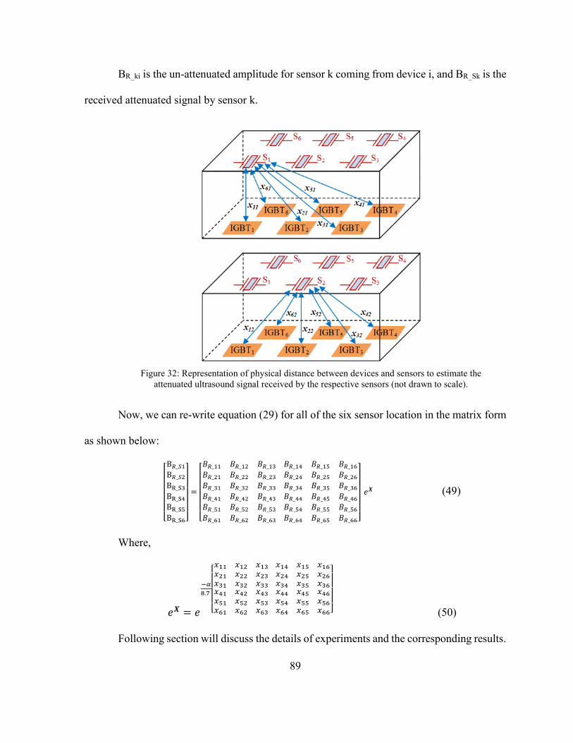
89
BR_ki is the un-attenuated amplitude for sensor k coming from device i, and BR_Sk is the
received attenuated signal by sensor k.
Now, we can re-write equation (29) for all of the six sensor location in the matrix form
as shown below:
[ B𝑅_𝑆1B𝑅_𝑆2BR_S3BR_S4BR_S5BR_S6]
=
[ 𝐵𝑅_11 𝐵𝑅_12 𝐵𝑅_13𝐵𝑅_21 𝐵𝑅_22 𝐵𝑅_23𝐵𝑅_31 𝐵𝑅_32 𝐵𝑅_33
𝐵𝑅_14 𝐵𝑅_15 𝐵𝑅_16𝐵𝑅_24 𝐵𝑅_25 𝐵𝑅_26𝐵𝑅_34 𝐵𝑅_35 𝐵𝑅_36
𝐵𝑅_41 𝐵𝑅_42 𝐵𝑅_43𝐵𝑅_51 𝐵𝑅_52 𝐵𝑅_53𝐵𝑅_61 𝐵𝑅_62 𝐵𝑅_63
𝐵𝑅_44 𝐵𝑅_45 𝐵𝑅_46𝐵𝑅_54 𝐵𝑅_55 𝐵𝑅_56𝐵𝑅_64 𝐵𝑅_65 𝐵𝑅_66]
𝑒𝑿 (49)
Where,
𝑒𝑿 = 𝑒
−𝛼
8.7
[ 𝑥11 𝑥12 𝑥13𝑥21 𝑥22 𝑥23𝑥31 𝑥32 𝑥33
𝑥14 𝑥15 𝑥16𝑥24 𝑥25 𝑥26𝑥34 𝑥35 𝑥36
𝑥41 𝑥42 𝑥43𝑥51 𝑥52 𝑥53𝑥61 𝑥62 𝑥63
𝑥44 𝑥45 𝑥46𝑥54 𝑥55 𝑥56𝑥64 𝑥65 𝑥66]
(50)
Following section will discuss the details of experiments and the corresponding results.
Figure 32: Representation of physical distance between devices and sensors to estimate the
attenuated ultrasound signal received by the respective sensors (not drawn to scale).
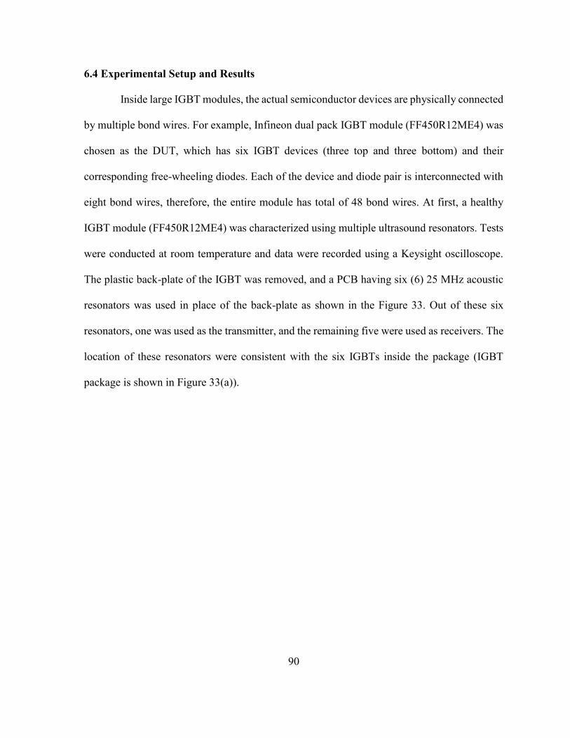
90
6.4 Experimental Setup and Results
Inside large IGBT modules, the actual semiconductor devices are physically connected
by multiple bond wires. For example, Infineon dual pack IGBT module (FF450R12ME4) was
chosen as the DUT, which has six IGBT devices (three top and three bottom) and their
corresponding free-wheeling diodes. Each of the device and diode pair is interconnected with
eight bond wires, therefore, the entire module has total of 48 bond wires. At first, a healthy
IGBT module (FF450R12ME4) was characterized using multiple ultrasound resonators. Tests
were conducted at room temperature and data were recorded using a Keysight oscilloscope.
The plastic back-plate of the IGBT was removed, and a PCB having six (6) 25 MHz acoustic
resonators was used in place of the back-plate as shown in the Figure 33. Out of these six
resonators, one was used as the transmitter, and the remaining five were used as receivers. The
location of these resonators were consistent with the six IGBTs inside the package (IGBT
package is shown in Figure 33(a)).
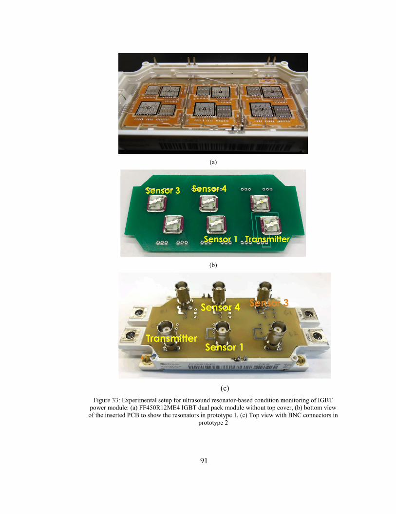
91
(a)
(b)
(c)
Figure 33: Experimental setup for ultrasound resonator-based condition monitoring of IGBT
power module: (a) FF450R12ME4 IGBT dual pack module without top cover, (b) bottom view
of the inserted PCB to show the resonators in prototype 1, (c) Top view with BNC connectors in
prototype 2

92
To create bond wire lift off incidents in a controlled manner, we disconnected multiple
bond wires in several locations rather than aging the IGBT using an accelerated aging station.
We intentionally did it to avoid uncertainty and quick turn-around time to validate our theory.
We also used a FLIR thermal camera to monitor the current crowding due to damaged bond
wires of a device inside the package. Figure 34(a) shows a healthy IGBT device with all eight
(8) bond wires intact. For this device the corresponding thermal image was uniform without
any significant hotspot. Figure 34(b) shows the actual photograph of the IGBT device with 3
bond wires detached, and the corresponding thermal image shows hotspot formation.
(a) Healthy device
(b) Aged device
Figure 34: Bond wire lift off and corresponding current crowding (the red circle shows damaged
bond wires).

93
Figure 35 and Figure 36 show the ultrasound results obtained from the onboard sensors
shown in Fig. 32(b). Figure 35 shows sensor 1 data in both time domain and frequency domain.
Figure 35(a) shows the time domain data with all bond wires intact, and Figure 35(b) shows
the time domain data when 3 bond wires are disconnected. Figure (c) and Figure (d) show the
frequency domain data for these two events respectively.
Figure 35: Time and frequency domain data from sensor 1

94
Figure 36 shows the time domain and frequency domain output signals obtained from
sensor 4, and the results have been compared with a healthy system. It is quite evident that for
any physical damage at any specific location, at least two sensors (sensors 1 and 4) produce
reduced time and frequency domain output compared to a healthy module. We have observed
similar response from sensors 3, and those results are shown in Figure 37. Sensor 1 detects a
reduction of 8.4dB, and sensor 4 detects a huge 12dB in the frequency domain output. These
reduced amplitudes are the clear indication of the IGBT’s bond wire lift off phenomenon.
Figure 36: Time and frequency domain data from sensor 4
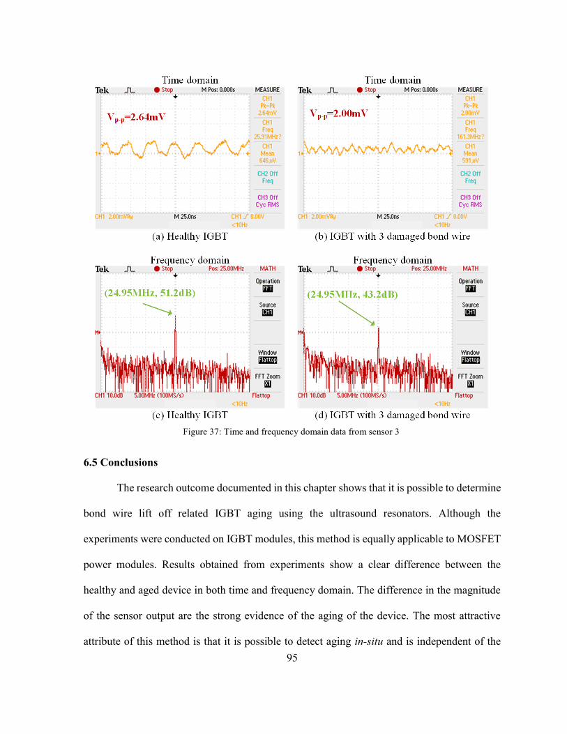
95
6.5 Conclusions
The research outcome documented in this chapter shows that it is possible to determine
bond wire lift off related IGBT aging using the ultrasound resonators. Although the
experiments were conducted on IGBT modules, this method is equally applicable to MOSFET
power modules. Results obtained from experiments show a clear difference between the
healthy and aged device in both time and frequency domain. The difference in the magnitude
of the sensor output are the strong evidence of the aging of the device. The most attractive
attribute of this method is that it is possible to detect aging in-situ and is independent of the
Figure 37: Time and frequency domain data from sensor 3

96
operating state of the modules- voltage and current levels. In addition, with proper scaling of
the resonators, this method can also be incorporated into the future gate driver circuits in order
to automate the state-of-health estimation process, making it more user-friendly as well as
reducing the human error in measurement phase associated with the existing condition
monitoring methods. However, there are several challenges associated with this method, and
further research is necessary to mitigate those in order to successfully implement in the field
applications. One of the major challenges for a successful field implementation is to determine
the optimum number of sensors to detect the device location. In addition, the resonator used to
verify the proposed methods are commercially available with steel enclosure, however, they
need to be sourced or manufactured such that they do not require any additional effort to deploy
in the field applications. Future research efforts will address all of these challenges.

97
CHAPTER 7
DEGRADATION DETECTION OF WIDE BANDGAP POWER DEVICES
7.1 Introduction
Silicon carbide (SiC) based power semiconductors are considered as a better
replacement of Si devices due to their superior switching speed, thermal conductivity and
breakdown electric field. Unfortunately SiC metal-oxide-semiconductor field-effect transistors
(MOSFETs) still have major limitations such as wafer defects, thermal runaway, electrical
breakdown, and so on [196] – [197] because of not so mature manufacturing process compared
to the Si counterpart. This fabrication related issue of SiC devices adversely affect the standard
operation of power converters leading to a total failure of the system. Researchers have been
continuously working on device reliability in order to better understand the failure modes and
mechanisms in the power semiconductor devices. In doing so, the devices under test (DUTs)
are aged in various methods considering the mission profiles to mimic the actual operating
environment. Among these methods, active power cycling, thermal cycling, and passive
thermal aging are the most commonly used techniques in recent times [103], [135], [198].
Active power cycling induces both the device related aging and package related aging,
whereas, the passive thermal cycling causes the package related degradation alone. However,
the ultimate target of an accelerated test is to age a device within a short time period and
identify the aging either by measuring electrical parameters or by incorporating a new
technique such as reflectometry. The electrical precursor parameter based detection could
provide erroneous degradation information if the measurement is not fast or accurate [199] –
[201]. In addition, this technique may not be used in a live circuit due to accessibility of the
measurement nodes. On the other hand, reflectometry based aging detection such as SSTDR
98
based method can be done in-situ as well as it is independent of measurement error since this
does not involve any electrical parameter measurement [41].
The traditional precursor parameter based aging detection having pros and cons can be
found in many literature [27], [172], [202]. The experimental data recorded in [200] are reliable
only if the MOSFET used in parallel with the DUT remains healthy over the time. In addition,
the entire converter may fail if the MOSFET becomes short. Another live condition monitoring
was achieved in [201], however, the results may provide inaccurate information if the
parameters of the diodes have measurement error.
Recently, SSTDR based fault detection technique is gaining momentum in wire fault
detection [39], [203], ground and arc fault detection in various photovoltaic applications [41]
– [42], and in degradation detection of power semiconductor devices [43]. In case of
MOSFETs, the SSTDR technique is able to identify the aging, however, it has never been used
in any reliability studies for SiC based power switches so far. In addition, the previous SSTDR
based methods applied the test signal either across the drain-source terminals or the output AC
nodes [43], [204]. On the contrary, the proposed method can detect the device aging from the
gate-source interface which remain at significantly lower potential compared to the drain-
source terminals. On top of that, it was not clearly addressed how the auto-correlated
amplitudes obtained from SSTDR hardware can be compared with the existing precursor
parameters such as RDSON. Through this research a direct correlation between the SSTDR
amplitude and RDSON of the MOSFET has been established. Therefore, this research will allow
us to estimate the aging of a power semiconductor device from the measurement of SSDTR
amplitudes. In addition, this method can be extended to any converter topology in order to
estimate the aging of the semiconductor devices.

99
Since this research work to identify the degradation of WBG devices based on SSTDR
is a pioneer work, we have carried out three case studies in order to verify the applicability of
the proposed method: (i) aging detection in discrete SiC MOSFETs, (ii) degradation detection
of a SiC MOSFET based buck converter, and (ii) aging detection of thermally aged SiC and Si
MOSFETs.
The experimental results suggest that SSTDR method is equally applicable to the WBG
power semiconductors as well as the proposed method is able to detect aging from the gate-
source terminals. As a result, the condition monitoring hardware can be designed at a
significantly lower rating which will create a provision to integrate the hardware with the gate
driver module of the power device.
The following sections of this chapter will discuss the method and case studies in
details.
7.2 Aging in MOSFETs: Equivalent Impedance Approach
7.2.1 Origin of Aging
Aging of a power semiconductor device is generally defined by significantly poor
electrical performance due to a change in electrical parameter. In addition, a device can
experience mechanical damage due to the environmental or electrical stress which is another
way to express the aging of a device. In both of the cases, it is highly likely that at least one of
the electrical parameters such as capacitance or ON-resistance will be affected over the course
of operation. Due to the manufacturing process and limitations, any MOSFET will have the
ON-resistance (RDSON) and parasitic capacitances between the terminals. A simplified
electrical equivalent circuit can be shown in Figure 38 [205].
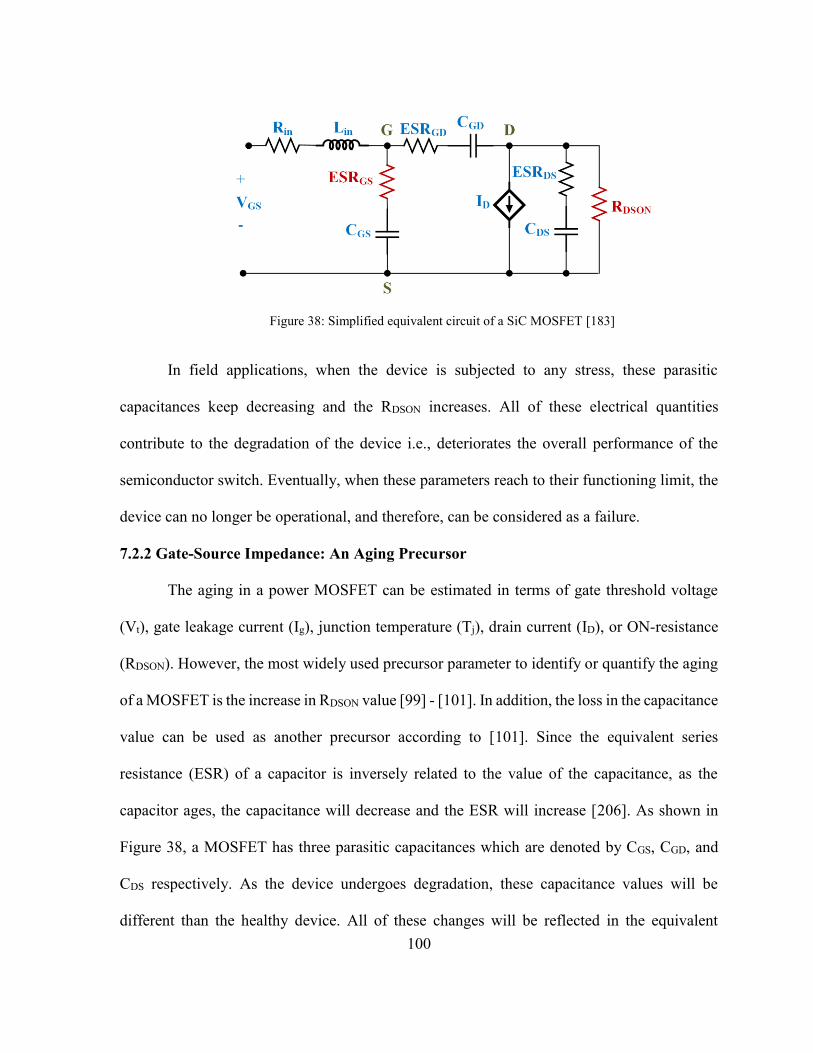
100
In field applications, when the device is subjected to any stress, these parasitic
capacitances keep decreasing and the RDSON increases. All of these electrical quantities
contribute to the degradation of the device i.e., deteriorates the overall performance of the
semiconductor switch. Eventually, when these parameters reach to their functioning limit, the
device can no longer be operational, and therefore, can be considered as a failure.
7.2.2 Gate-Source Impedance: An Aging Precursor
The aging in a power MOSFET can be estimated in terms of gate threshold voltage
(Vt), gate leakage current (Ig), junction temperature (Tj), drain current (ID), or ON-resistance
(RDSON). However, the most widely used precursor parameter to identify or quantify the aging
of a MOSFET is the increase in RDSON value [99] - [101]. In addition, the loss in the capacitance
value can be used as another precursor according to [101]. Since the equivalent series
resistance (ESR) of a capacitor is inversely related to the value of the capacitance, as the
capacitor ages, the capacitance will decrease and the ESR will increase [206]. As shown in
Figure 38, a MOSFET has three parasitic capacitances which are denoted by CGS, CGD, and
CDS respectively. As the device undergoes degradation, these capacitance values will be
different than the healthy device. All of these changes will be reflected in the equivalent
Figure 38: Simplified equivalent circuit of a SiC MOSFET [183]

101
impedance seen between the gate (G) and source (S) terminals (ZGS), and the value before and
after aging will be different. Hence this change can be used in estimating the overall
degradation of the semiconductor device.
Let, the equivalent impedance seen across gate and source terminals of a healthy device
is denoted by ZGS_H, and due to degradation, the equivalent impedance is ZGS_A. If the
difference in equivalent impedance between a healthy and an aged device is denoted by ΔZGS,
the relationship between these three quantities can be written as:
|ZGS_H – ZGS_A| = ΔZGS (51)
Since the SSTDR hardware is sensitive to the impedance variation, even if the changes
are minor, this change (ΔZGS) can be detected by the hardware. If the change in the equivalent
impedance is a non-zero value, the SSTDR will produce two distinct data sets for a healthy
device and aged device. Thus the SSTDR can be used in estimating the aging of a MOSFET
from the gate-source terminals.
7.3 Case Study-1: Degradation Detection in a Discrete SiC MOSFET
In this section, the degradation of a SiC MOSFET from the gate-source interface has
been studied. The online condition monitoring was achieved by Spread Spectrum Time
Domain Reflectometry (SSTDR) for the first time in SiC based devices. An accelerated aging
station was built to age the power semiconductor devices in a standardized way, and power
cycling test was performed to induce degradation. Finally, the SSTDR data, before and after
aging, were compared and plotted in order to identify the degradation from the gate terminal
of the device. This proposed method can rely on monitoring only gate-source interface
meaning it does not involve any high voltage at the drain.

102
7.3.1 Standardized Accelerated Aging Methodology
An accelerated aging station was built in order to induce the degradation in SiC
MOSFET. The aging station, shown in Figure 39, consists of a DC power supply, gate drive
circuit, data acquisition system, current sensor, thermocouple, and device under test (DUT i.e.
SiC MOSFET). A 1200V, 90A rated SiC power MOSFET, shown in Figure 40,
(C2M0025120D, manufactured by CREE Inc.) was selected as the DUT. Power cycling was
performed, and a total 4000 cycles were recorded by the data acquisition system until the aging
process was completed. During the test, LabJack T-7 Pro data acquisition system (DAQ) was
used to measure and record VDS, ID and case temperature (Tcase). The case temperature was
measured using a K-type thermocouple from OMEGA, and an Arduino based controller was
used to control the entire process. The ON-state resistance for the new MOSFET was measured
29mΩ, and after 4000 aging cycles, it was increased to 34mΩ. This indicates an aging level of
about 17%. Both readings were taken at the junction temperature of 25° C. In order to age the
DUT faster, it was not attached to any heat sink, and forced air was used to drop the case
temperature faster during the turn-OFF period.
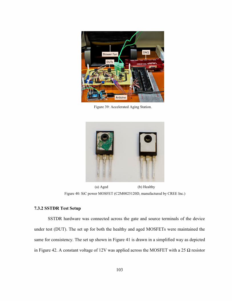
103
7.3.2 SSTDR Test Setup
SSTDR hardware was connected across the gate and source terminals of the device
under test (DUT). The set up for both the healthy and aged MOSFETs were maintained the
same for consistency. The set up shown in Figure 41 is drawn in a simplified way as depicted
in Figure 42. A constant voltage of 12V was applied across the MOSFET with a 25 Ω resistor
Figure 39: Accelerated Aging Station.
(a) Aged (b) Healthy
Figure 40: SiC power MOSFET (C2M0025120D, manufactured by CREE Inc.)
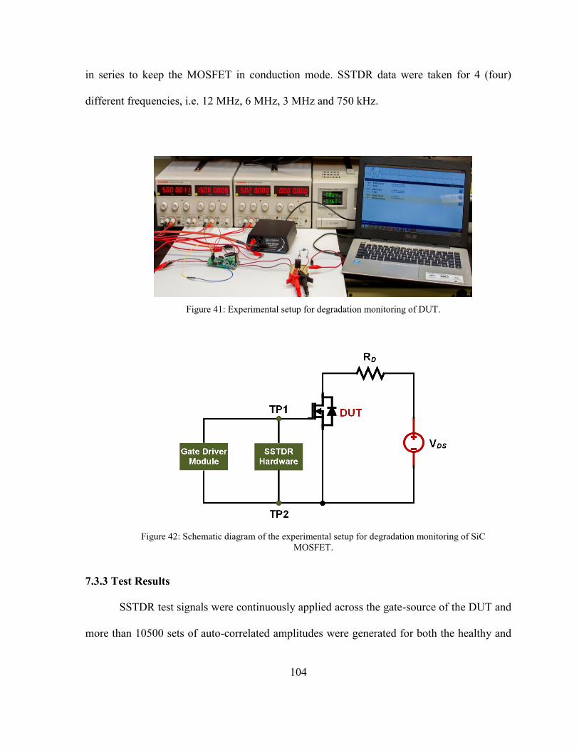
104
in series to keep the MOSFET in conduction mode. SSTDR data were taken for 4 (four)
different frequencies, i.e. 12 MHz, 6 MHz, 3 MHz and 750 kHz.
7.3.3 Test Results
SSTDR test signals were continuously applied across the gate-source of the DUT and
more than 10500 sets of auto-correlated amplitudes were generated for both the healthy and
Figure 41: Experimental setup for degradation monitoring of DUT.
Figure 42: Schematic diagram of the experimental setup for degradation monitoring of SiC
MOSFET.

105
aged MOSFET for each SSTDR frequencies. All these auto-correlated amplitudes were
averaged and plotted in Figure 43 and a portion of the plot was zoomed for better clarity. These
plots clearly show that the auto-correlated peak amplitudes for aged device are always less in
magnitude than that of the healthy one. This variation was expected because the magnitude of
the correlated amplitude is proportional to reflection coefficient (Γ) and any increase in the
ESR of the gate-source capacitance and the ON-state resistance for an aged MOSFET will
eventually lead to less positive values of them compared to the new MOSFET [207].
.
Figure 43: SSTDR auto-correlation plots for new and aged SiC MOSFETs at different SSTDR frequencies
recorded from the gate-source terminals.

106
7.4 Case Study-2: Degradation detection in a SiC based buck converter
The widely-used buck converter has been chosen for this study, although the proposed
method can be used with any power converter. Over the course of the operation, various
components in a buck converter degrade, and their electrical characteristics change. In other
words, if a device is physically damaged or the electrical performance of the device is
significantly degraded, the device can be considered aged. A degradation associate to any
single component is likely to propagate through the entire circuit and would alter the circuit’s
electrical characteristics. Therefore, it becomes very difficult to determine aging levels when
multiple devices age simultaneously. To begin with, one aged device has been considered in
the entire converter, and the SSTDR based degradation detection have been studied. Figure 44
shows the schematic of a buck converter, and the SiC MOSFET (M) is the device under test
(DUT), which will eventually undergo aging. Since all other components of the buck converter
will remain unaffected, the impedance variation of the SiC MOSFET will provide the
impression of the overall buck converter’s degradation. In most cases, the degradation level in
a MOSFET is quantified by measuring the rise in RDSON [99] - [101].

107
7.4.1 Aging in Buck Converter
The equivalent impedance of a healthy buck converter can be defined as Zbuck_H when
seen across the gate and source terminals of the SiC MOSFET. Due to any degradation, the
changes in the parasitic capacitances and in the ON-state resistance of the SiC MOSFET will
affect the equivalent impedance of the MOSFET, as well as the equivalent impedance of the
buck converter seen across those terminals. Consider, the equivalent impedance of the buck
converter due to the aged device is Zbuck_A when seen from the gate-source interface of the
MOSFET. Now, if ΔZbuck is defined as the net impedance change within the buck converter
when seen across the gate and source terminal of the MOSFET, then the difference in
equivalent impedance between a healthy and an aged converter can be written as:
|Zbuck_H – Zbuck_A| = ΔZbuck (52)
This impedance variation can easily be detected by the SSTDR hardware because it is
able to identify any impedance mismatch on the SSTDR signal’s path of propagation. Now, if
the SSTDR data were taken for a healthy and a degraded buck converter, this impedance
Figure 44: Schematic of a SiC MOSFET based buck converter

108
mismatch of ΔZbuck, even if the magnitude is minor, can be correlated by the magnitude
difference between the two readings. It will distinctly indicate the aging of the buck converter
if and only if the magnitude of ΔZbuck is a non-zero value.
7.4.2 Experimental Setup
A buck converter prototype was built, and the SiC MOSFET was selected as the
switching device. The device under test was rated for 1200V, 90A, and manufactured by CREE
Inc. Before starting any accelerated aging process, SSTDR data was recorded for the healthy
converter across the gate and source terminal of the MOSFET, and this data will be considered
as the reference for future analysis. The overall experimental process consists of three major
steps, namely, SSTDR data collection for the healthy device, power cycling of the DUT, and
SSTDR data accumulation for aged DUT within the buck converter.
7.4.2.1 Power Cycling of SiC MOSFET
The DUT was aged by active power cycling method. The case temperature was
monitored by using a K-type thermocouple, and the temperature swing was 80°C (ΔT), starting
from 100°C (Tmin) and ending at 180°C (Tmax). In order to make sure that the thermocouple
was in good contact with the MOSFET case, a highly thermal conductive pad was used to
reduce any unwanted air gap between the tip of the thermocouple and the case of the SiC
MOSFET. Forced air was provided using a blower fan to cool down the MOSFET during the
OFF-state. Once the case temperature reached 100°C, the device was turned ON and air flow
was stopped, and these controls were established with the help of an Arduino UNO
microcontroller. The time required to increase the case temperature from 100°C to 180°C and
bring it back to 100°C was defined as a complete cycle, and a total of 4000 cycles were
recorded by the data acquisition system before the device was sufficiently degraded. Using a

109
DC power supply, a current flow of 24A was supplied to the drain of the device under test.
Since the DUT for this experiment had a very low ON-resistance compared to any similarly
rated Si MOSFET, it required additional current (to be injected) as well as higher number of
cycles to induce any equivalent amount of aging. Figure 45 shows the accelerated power
cycling station used in this experiment.
7.4.2.2 SSTDR Test Setup
SSTDR measurement setup parameters were maintained identical for both the healthy
and aged buck converter in order to be consistent. Figure 46 depicts the setup for recording the
SSTDR readings of a SiC based buck converter, for both healthy and aged devices. The
simplified schematic of the SSTDR measurement setup is presented in Figure 47. Readings
were taken across the gate and source terminals of the DUT (SiC MOSFET) located inside the
buck converter while it was turned ON, i.e., at steady state condition. The SSTDR signal was
continuously applied at the frequencies of 3MHz, 6MHz, 12MHz, and 48MHz in order to
generate multiple sets of data.
Figure 45: Power cycling station

110
7.4.3 Test Results
Power cycling of the SiC MOSFET was initiated after taking the SSTDR data for the
healthy device. At the same time, the RDSON was measured in order to compare the degradation
level induced from power cycling. All the readings for both the healthy and aged buck
converter were taken at the same room temperature. The aim was to detect aging by the well-
known precursor parameter, RDSON, and then compare the two SSTDR readings, before and
after aging, to identify the aging.
Figure 46: Buck converter setup to apply SSTDR
Figure 47: Buck converter setup to apply SSTDR

111
To achieve the above mentioned goal, first RDSON was measured for the healthy device,
and it was 27mΩ. After 4000 cycles, RDSON was measured again at room temperature, and the
new RDSON was 31 mΩ i.e., the change in RDSON was 4mΩ. This is equivalent to 15% variation
compared to the initial value. In the next step, SSTDR data was recorded across the gate and
source terminal of the DUT. The SSTDR signal was continuously applied and close to 1700
sets of data were generated for both of the healthy and aged buck converter at each frequency.
All of these data were averaged and plotted. These auto-correlated SSTDR amplitudes taken
at 3MHz, 6MHz, 12MHz, and 48MHz frequencies are plotted in Figure 48. These plots show
that the amplitude at the peak of interest for the aged converter is less in magnitude than the
healthy peak (the first peak is due to the artifact of the hardware and the second peak comes
from the probe end at the hardware side). This behavior was expected, as both ESR of gate
capacitances and RDSON will increase with aging, and together will lead to a lower reflection
coefficient, resulting in a lower magnitude of SSTDR amplitude [203]. However, to observer
the changes with better lucidity, the peak of interest was zoomed and included within the plots.
The non-zero magnitude difference between the healthy and aged amplitudes prove the aging
of the buck converter.

112
7.5 Case Study-3: Degradation Detection of Thermally Aged Si and SiC Power
MOSFET
In this section, degradation detection of Si and SiC MOSFET based on SSTDR have
been studied. The auto-correlated amplitude obtained from SSTDR hardware have been
compared with the existing precursor parameter (RDSON) as well. A direct correlation between
the SSTDR amplitude and RDSON of the MOSFET has been established through this research
work. Therefore, this research will allow us to estimate the aging of a power semiconductor
device from the measurement of SSDTR amplitudes. In addition, this method can be extended
to any converter topology in order to estimate the aging of the semiconductor devices.
Figure 48: SSTDR auto-correlated amplitude plots for healthy and aged buck converter at different
frequencies

113
7.5.1 Experimental Setup
The primary objective of this research work was to detect the degradation induced from
passive thermal aging using SSTDR technique. The overall process consists of four steps
which can be listed as below:
i. Collection of SSTDR data and RDSON values for healthy devices.
ii. Induce thermal aging in an environment chamber for all of the devices under test
(DUTs).
iii. Recording SSTDR and RDSON data for the aged devices.
iv. Compare the data obtained in steps i and iii in order to establish a correlation
between the RDSON and SSTDR data sets.
In order to accomplish the above mentioned steps two experimental setup was required
namely thermal aging station and SSTDR test setup which are described below:
7.5.1.1 Passive Thermal Aging Station
Two (2) silicon carbide (SiC) MOSFETs and two (2) Si MOSFETs were selected as
the DUT to undergo thermal aging. The SiC MOSFETs were rated for 1200V, 90A, and
manufactured by Cree. On the other hand, Si MOSFETs were rated for 600V, 50A, and these
voltage and current ratings are almost half of the SiC voltage and current MOSFETs. This was
intentionally and wisely chosen to compare the relative reliability of SiC and Si MOSFETs.
All of these DUTs were aged in a DELTA environment chamber at a temperature of 150°C.
RDSON values were measured and recorded while the MOSFETs were in full conduction for
every 10hrs of aging at the room temperature. RDSON values were recorded for three different
current levels and averaged for each device to avoid the measurement uncertainty. The DELTA
environment chamber is shown in Figure 49.

114
7.5.1.2 SSTDR Test Setup
SSTDR measurements were taken between the gate and source terminals of the
MOSFETs. The devices were in full conduction while recording the data. In addition, the
settings in the SSTDR parameters were maintained the same throughout the experiments in
order to keep consistency in the data. The actual SSTDR test setup is depicted in Figure 50,
and Figure 51 illustrates the simplified schematic of the SSTDR measurement.
Figure 49: DELTA thermal aging chamber

115
Figure 50: SSTDR test setup
Figure 51. Schematic of the SSTDR experimental setup for degradation monitoring.

116
7.5.2 Test Results
All of the experimental data were recorded at room temperature for each device. In
order to maintain the same junction and case temperature of the MOSFETs, the devices were
cooled down to the room temperature with a waiting period of 12hrs before taking any
measurement. A device was considered to be significantly aged when the change in the RDSON
value was twenty percent (20%) of its initial value. And, after about 100hrs of thermal aging
all four of the devices showed nearly 20% increase in their preliminary ON-resistance. The
average RDSON values recorded every 10hr of aging are plotted and shown in Figure 52 for all
of the MOSFETs.
SSTDR test signals were continuously applied across the gate-source of the DUTs
while the devices were in full conduction. The SSTDR center frequency was set at 48MHz and
more than 3300 sets of auto-correlated amplitudes were generated and averaged for each device
in both of the healthy and aged conditions. These auto-correlated data are plotted in Figure 53
Figure 52: Changes in RDSON over time.

117
for Si MOSFETs, and Figure 54 shows the plots for SiC devices. Peak of interests have been
zoomed and included within the respective plots for better visualization of the distinct data
points between the healthy and aged devices. The variation in these data for healthy device,
50hr aged DUT, and 100hr aged DUT show a decreasing trend which is consistent with the
reflectometry theory as stated in equation (19). The equivalent impedance between the gate-
source terminals of the DUT (ZGS) can be considered as the ZL in equation (19). As the device
ages, the magnitude of ZGS increases due to the loss in parasitic capacitances and increase in
the RDSON value. So, for an aged device the equivalent impedance seen between the gate and
source terminals (ZGS_A) is higher than the impedance of a healthy device (ZGS_H). Therefore,
the reflection coefficient i.e., SSTDR peak amplitude decreases with increasing impedance
seen by the SSTDR hardware.
Figure 53: SSTDR auto-correlation plots for new and aged Si MOSFETs at 48MHz SSTDR frequency

118
It is important to establish a correlation between the traditional precursor parameter (in
this case RDSON) and the SSTDR auto-correlated peaks. Table XII shows the changes in the
RDSON values and SSTDR peak amplitudes for all of the DUTs after 50hrs and 100hrs of aging.
Interestingly, the percent change in SSTDR amplitude after 50hrs and 100hrs of aging are
about twice the percent change in the corresponding RDSON values. Hence, it is possible to
estimate the failure from the SSTDR amplitude without measuring any electrical parameters.
Interestingly, SiC devices show the similar change in their RDSON values although they have
the double voltage and current rating compared to the Si MOSFETs. This is because the
manufacturing process is not yet as mature as the process of Si technology, and therefore, the
SiC MOSFETs are still less reliable than the existing Si devices.
The correlation between the relative changes in RDSON and SSTDR auto-correlated peak
amplitude can be better understood from Figure 55. The trend in data for both RDSON and
SSTDR peak amplitude shows the linear relationship with the aging of the devices.
Figure 54: SSTDR auto-correlation plots for new and aged SiC MOSFETs at 48MHz SSTDR
frequency
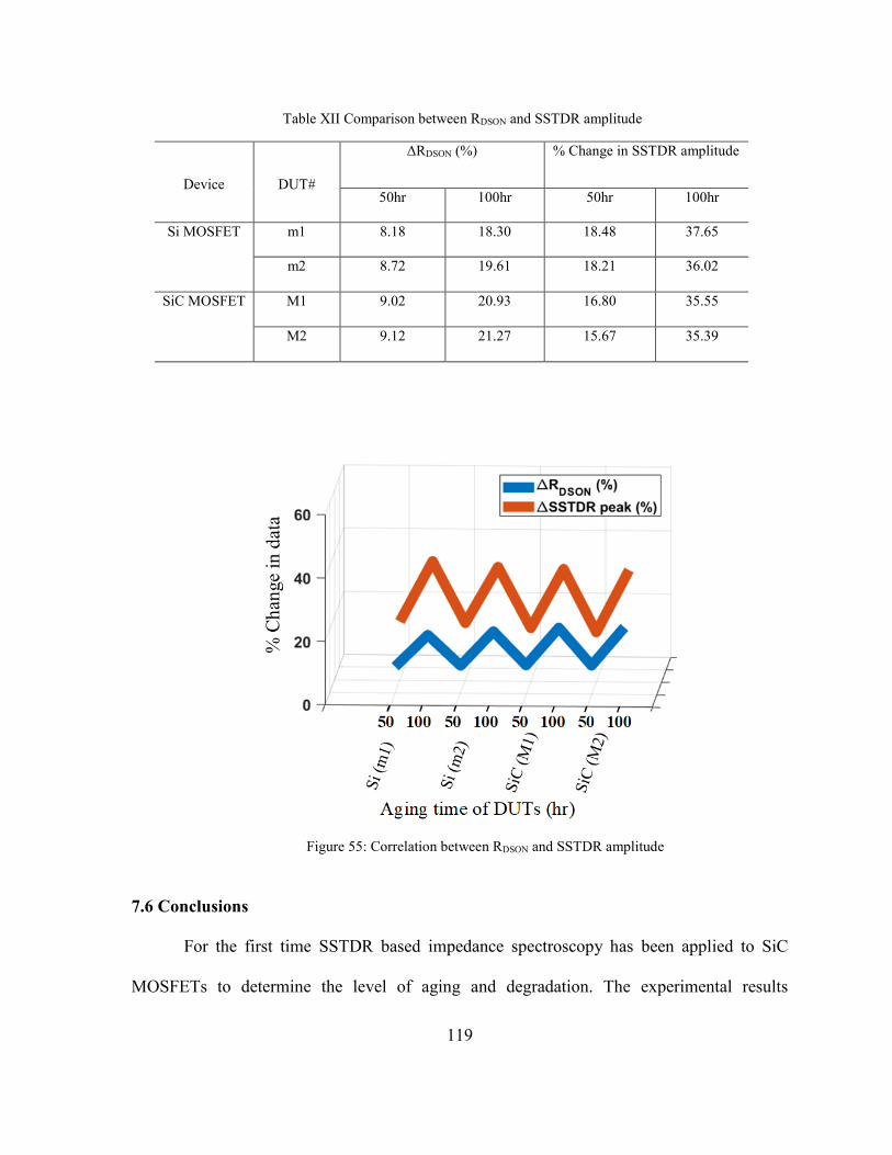
119
7.6 Conclusions
For the first time SSTDR based impedance spectroscopy has been applied to SiC
MOSFETs to determine the level of aging and degradation. The experimental results
Table XII Comparison between RDSON and SSTDR amplitude
Device
DUT#
ΔRDSON (%) % Change in SSTDR amplitude
50hr 100hr 50hr 100hr
Si MOSFET m1 8.18 18.30 18.48 37.65
m2 8.72 19.61 18.21 36.02
SiC MOSFET M1 9.02 20.93 16.80 35.55
M2 9.12 21.27 15.67 35.39
Figure 55: Correlation between RDSON and SSTDR amplitude

120
demonstrate that it is possible to estimate the state of health of a SiC MOSFET as well as of a
SiC-based buck converter using SSTDR. In addition, this research work establishes a bridge
between the most widely used precursor parameter of a MOSFET (RDSON) and the emerging
SSTDR based aging detection (auto-correlated peaks). According to the experimental data, Si
devices are still better switching devices in terms of the thermal reliability. Although, the SiC
devices have high power density compared to Si, they still suffer from maturity in
manufacturing process to compete with the similar rated Si counterparts.
Unlike previous SSTDR applications, the research outcome can determine aging
associated with miniscule changes inside a SiC MOSFET connected to a branched network
(buck converter), and the technique can be applied to a live circuit. Another unique feature of
this work is that the SSTDR was applied between the gate and source terminal of the SiC power
MOSFET when the device was in full conduction. Rather than applying the SSTDR across the
drain-source terminal, it has been applied across the gate-source interface for several reasons.
First of all, the drain terminal is not always accessible is real converters. In addition, since the
drain side is at the higher potential, the possibility of human injury is more. On the other hand,
the gate side is limited to 18V for SiC MOSFETs and always accessible for any converter.
Since the gate oxide layer in SiC MOSFET is the most vulnerable part, it is a necessity to
identify the aging in the oxide layer while the circuit is live. Although these experiments were
conducted for a single SiC MOSFET, it is possible to identify the level of aging associated to
an individual MOSFET in a 3-phase H-bridge module by applying SSTDR at the gate and
source terminals only. On top of that, the proposed method creates a provision to redesign the
SSTDR hardware at a significantly lower rating and then the condition monitoring unit can be
integrated with the gate driver module which will further reduce the overall cost. Moreover,

121
unlike traditional condition monitoring methods, the SSTDR based aging detection does not
require measuring any electrical parameters which ensures zero measurement error. Thus, this
method clearly shows advantages compared to other existing condition monitoring techniques.

122
CHAPTER 8
CONCLUSIONS AND FUTURE RESEARCH
The primary objective of any condition monitoring method is to find the remaining
useful life of a power semiconductor device or a power converter. The knowledge of the mean
time to failure of a device helps in scheduling the periodic maintenance and ultimately enhance
the operational life of that device as well as reduce the overall cost of the system level
maintenance. This dissertation presents a comprehensive solution to determine the state of
health of a power semiconductor device in a live power converter using online in-situ, non-
invasive technique based on spread spectrum time domain reflectometry (SSTDR) and
ultrasound resonator.
Unlike traditional degradation detection methods, the proposed SSTDR based aging
detection does not require measuring any failure precursor parameters such as voltage or
current, and therefore, it eliminates the measurement uncertainties in live power converters.
Until today, the SSTDR-based SOH monitoring techniques were only able to detect device
degradation from the high voltage terminals (drain or collector side). It is worth to mention
that the existing methods are able to detection aging while the converter is in idle state whereas
the propose method is able to perform condition monitoring of a device or converter circuit
regardless of its operating states (live or off-line) and from the gate-source or gate-emitter
interface. Therefore, the SSTDR based method creates a provision to integrate the condition
monitoring hardware with the gate drive module. So, the SSTDR based condition monitoring
or sate of health estimation method opens a new avenue in the field of reliability and the future
work will address the following challenges:
123
(i) The existing SSTDR hardware is only limited to 48MHz of center frequency.
Therefore, a redesign of the SSTDR hardware is necessary so that it is able to send
higher frequency signals. This will also increase the resolution of the defect detection.
(ii) Since the proposed method is able to detect device degradation from the gate terminals
of both MOSFET and IGBT, it is natural to shift the research direction in developing a
comprehensive solution of condition monitoring hardware by integrating the
redesigned SSTDR hardware with the gate driver module.
(iii) The proposed method relies on the equivalent impedance of the device of the converter
seen from the gate-source terminals, thus it is unable to differentiate the channel and
gate-oxide layer degradation. Since gate oxide layer is the most vulnerable part of a
SiC MOSFET, it is necessary to extend the research area toward decoupling the channel
and gate-oxide degradation by extracting the transmission line model parameters of the
SSTDR propagation path.
This manuscript also presents the bond wire related degradation detection of IGBT
power modules using ultrasound resonators. The proof-of-concept results have been included
in chapter 6 where it has been demonstrated that the proposed ultrasound based non-destructive
evaluation is able to identify the bond wire failure (lift-off) related IGBT module failures. This
research has established similar future research scopes as stated above since the proposed
method is independent of the module’s operating condition. However, the preliminary results
do not explain the mutual relationship between the resonator frequency and the number of bond
wire lift offs. Therefore, the natural direction of future research efforts includes finding the
optimum number of resonators, their respective location, and the optimum frequencies of the
resonator to identify the location and number of the affected bond wires.

124
REFERENCES
[1] A. Ristow, M. Begovic, A. Pregelj and A. Rohatgi, "Development of a Methodology for
Improving Photovoltaic Inverter Reliability," in IEEE Transactions on Industrial Electronics,
vol. 55, no. 7, pp. 2581-2592, July 2008, doi: 10.1109/TIE.2008.924017.
[2] S. E. De León-Aldaco, H. Calleja, F. Chan and H. R. Jiménez-Grajales, "Effect of the
Mission Profile on the Reliability of a Power Converter Aimed at Photovoltaic Applications—
A Case Study," in IEEE Transactions on Power Electronics, vol. 28, no. 6, pp. 2998-3007,
June 2013, doi: 10.1109/TPEL.2012.2222673.
[3] F. Chan and H. Calleja, "Reliability Estimation of Three Single-Phase Topologies in Grid-
Connected PV Systems," in IEEE Transactions on Industrial Electronics, vol. 58, no. 7, pp.
2683-2689, July 2011, doi: 10.1109/TIE.2010.2060459.
[4] M. K. Alam and F. H. Khan, "Reliability Analysis and Performance Degradation of a Boost
Converter," in IEEE Transactions on Industry Applications, vol. 50, no. 6, pp. 3986-3994,
Nov.-Dec. 2014, doi: 10.1109/TIA.2014.2319587.
[5] Y. Ding, P. C. Loh, K. K. Tan, P. Wang and F. Gao, "Reliability evaluation of three-level
inverters," 2010 Twenty-Fifth Annual IEEE Applied Power Electronics Conference and
Exposition (APEC), Palm Springs, CA, USA, 2010, pp. 1555-1560, doi:
10.1109/APEC.2010.5433438.
[6] M. R. A, U. B S and S. K, "A fault tolerant dual inverter configuration for islanded mode
photovoltaic generation system," 2013 1st International Future Energy Electronics
Conference (IFEEC), Tainan, Taiwan, 2013, pp. 816-821, doi: 10.1109/IFEEC.2013.6687614.

125
[7] M. T. Dat, T. Wijnhoven and J. Driesen, "Fault-tolerant topology of a grid-connected PV
inverter coupled by a Scott transformer," 2012 10th International Power & Energy Conference
(IPEC), Ho Chi Minh City, Vietnam, 2012, pp. 428-433, doi: 10.1109/ASSCC.2012.6523306.
[8] A. Tajfar and S. K. Mazumder, "A fault-tolerant switching scheme for a photovoltaic high-
frequency-link inverter," 2012 Twenty-Seventh Annual IEEE Applied Power Electronics
Conference and Exposition (APEC), Orlando, FL, USA, 2012, pp. 2087-2094, doi:
10.1109/APEC.2012.6166109.
[9] Y. Xiong, X. Cheng, Z. J. Shen, C. Mi, H. Wu and V. K. Garg, "Prognostic and Warning
System for Power-Electronic Modules in Electric, Hybrid Electric, and Fuel-Cell Vehicles," in
IEEE Transactions on Industrial Electronics, vol. 55, no. 6, pp. 2268-2276, June 2008, doi:
10.1109/TIE.2008.918399.
[10] S. Mohagheghi, R. G. Harley, T. G. Habetler and D. Divan, "Condition Monitoring of
Power Electronic Circuits Using Artificial Neural Networks," in IEEE Transactions on Power
Electronics, vol. 24, no. 10, pp. 2363-2367, Oct. 2009, doi: 10.1109/TPEL.2009.2017806.
[11] S. Zhou, L. Zhou and P. Sun, "Monitoring Potential Defects in an IGBT Module Based
on Dynamic Changes of the Gate Current," in IEEE Transactions on Power Electronics, vol.
28, no. 3, pp. 1479-1487, March 2013, doi: 10.1109/TPEL.2012.2210249.
[12] D. Xiang, L. Ran, P. Tavner, S. Yang, A. Bryant and P. Mawby, "Condition Monitoring
Power Module Solder Fatigue Using Inverter Harmonic Identification," in IEEE Transactions
on Power Electronics, vol. 27, no. 1, pp. 235-247, Jan. 2012, doi:
10.1109/TPEL.2011.2160988.
[13] D. Xiang, L. Ran, P. Tavner, A. Bryant, S. Yang and P. Mawby, "Monitoring Solder
Fatigue in a Power Module Using Case-Above-Ambient Temperature Rise," in IEEE

126
Transactions on Industry Applications, vol. 47, no. 6, pp. 2578-2591, Nov.-Dec. 2011, doi:
10.1109/TIA.2011.2168556.
[14] S. Haumann, J. Rudzki, F. Osterwald, M. Becker and R. Eisele, "Novel bonding and
joining technology for power electronics - Enabler for improved lifetime, reliability, cost and
power density," 2013 Twenty-Eighth Annual IEEE Applied Power Electronics Conference and
Exposition (APEC), Long Beach, CA, USA, 2013, pp. 622-626, doi:
10.1109/APEC.2013.6520275.
[15] R. Schmidt, C. König and P. Prenosil “Novel wire bond material for advanced power
module packages,” Microelectron. Rel. vol. 52, no. 9-10, pp. 2283–2288, 2012.
[16] T. Krebs, S. Duch, W. Schmitt, S. Kötter, P. Prenosil and S. Thomas, "A breakthrough in
power electronics reliability — New die attach and wire bonding materials," 2013 IEEE 63rd
Electronic Components and Technology Conference, Las Vegas, NV, USA, 2013, pp. 1746-
1752, doi: 10.1109/ECTC.2013.6575811.
[17] Y. Song and B. Wang, "Survey on Reliability of Power Electronic Systems," in IEEE
Transactions on Power Electronics, vol. 28, no. 1, pp. 591-604, Jan. 2013, doi:
10.1109/TPEL.2012.2192503.
[18] D. Li and X. Li, "Study of Degradation in Switching Mode Power Supply Based on the
Theory of PoF," 2012 International Conference on Computer Science and Service System,
Nanjing, China, 2012, pp. 1976-1980, doi: 10.1109/CSSS.2012.493.
[19] S. Das, F. Khan, M. K. Alam and P. Goli, "Detection of aging related IGBT bond-wire
lift-off using spread spectrum time domain reflectometry (SSTDR)," 2017 IEEE Applied
Power Electronics Conference and Exposition (APEC), Tampa, FL, 2017, pp. 789-794, doi:
10.1109/APEC.2017.7930785.
127
[20] S. Yang, A. Bryant, P. Mawby, D. Xiang, L. Ran and P. Tavner, "An Industry-Based
Survey of Reliability in Power Electronic Converters," in IEEE Transactions on Industry
Applications, vol. 47, no. 3, pp. 1441-1451, May-June 2011, doi: 10.1109/TIA.2011.2124436.
[21] A. Volke, and M. Hornkamp, IGET Modules - Technologies, Driver and Application,
Infineon Technologies AG, 2011. ISBN: 978-3-00-0320767.
[22] S. Yang, D. Xiang, A. Bryant, P. Mawby, L. Ran and P. Tavner, "Condition Monitoring
for Device Reliability in Power Electronic Converters: A Review," in IEEE Transactions on
Power Electronics, vol. 25, no. 11, pp. 2734-2752, Nov. 2010, doi:
10.1109/TPEL.2010.2049377.
[23] N. Patil, D. Das, K. Goebel and M. Pecht, "Identification of failure precursor parameters
for Insulated Gate Bipolar Transistors (IGBTs)," 2008 International Conference on
Prognostics and Health Management, Denver, CO, USA, 2008, pp. 1-5, doi:
10.1109/PHM.2008.4711417.
[24] A. E. Ginart, D. W. Brown, P. W. Kalgren and M. J. Roemer, "Online Ringing
Characterization as a Diagnostic Technique for IGBTs in Power Drives," in IEEE Transactions
on Instrumentation and Measurement, vol. 58, no. 7, pp. 2290-2299, July 2009, doi:
10.1109/TIM.2009.2013920.
[25] D. W. Brown, M. Abbas, A. Ginart, I. N. Ali, P. W. Kalgren and G. J. Vachtsevanos,
"Turn-Off Time as an Early Indicator of Insulated Gate Bipolar Transistor Latch-up," in IEEE
Transactions on Power Electronics, vol. 27, no. 2, pp. 479-489, Feb. 2012, doi:
10.1109/TPEL.2011.2159848.
[26] M. Tlig, J. Ben Hadj Slama and M. A. Belaid, "Experimental study on the EMI and
switching time evolution of IGBT devices after operating aging tests," 2014 International

128
Conference on Electrical Sciences and Technologies in Maghreb (CISTEM), Tunis, Tunisia,
2014, pp. 1-5, doi: 10.1109/CISTEM.2014.7076991.
[27] V. Smet, F. Forest, J. Huselstein, A. Rashed and F. Richardeau, "Evaluation of Vce
Monitoring as a Real-Time Method to Estimate Aging of Bond Wire-IGBT Modules Stressed
by Power Cycling," in IEEE Transactions on Industrial Electronics, vol. 60, no. 7, pp. 2760-
2770, July 2013, doi: 10.1109/TIE.2012.2196894.
[28] V. Smet et al., "Ageing and Failure Modes of IGBT Modules in High-Temperature Power
Cycling," in IEEE Transactions on Industrial Electronics, vol. 58, no. 10, pp. 4931-4941, Oct.
2011, doi: 10.1109/TIE.2011.2114313.
[29] U. Choi, S. Jørgensen and F. Blaabjerg, "Advanced Accelerated Power Cycling Test for
Reliability Investigation of Power Device Modules," in IEEE Transactions on Power
Electronics, vol. 31, no. 12, pp. 8371-8386, Dec. 2016, doi: 10.1109/TPEL.2016.2521899.
[30] U. Choi, I. Trintis, F. Blaabjerg, S. Jørgensen and M. L. Svarre, "Advanced power cycling
test for power module with on-line on-state VCE measurement," 2015 IEEE Applied Power
Electronics Conference and Exposition (APEC), Charlotte, NC, USA, 2015, pp. 2919-2924,
doi: 10.1109/APEC.2015.7104765.
[31] M. A. Eleffendi and C. M. Johnson, "Evaluation of on-state voltage VCE(ON) and threshold
voltage Vth for real-time health monitoring of IGBT power modules," 2015 17th European
Conference on Power Electronics and Applications (EPE'15 ECCE-Europe), Geneva,
Switzerland, 2015, pp. 1-10, doi: 10.1109/EPE.2015.7309265.
[32] A. Alghassi, S. Perinpanayagam, M. Samie and T. Sreenuch, "Computationally Efficient,
Real-Time, and Embeddable Prognostic Techniques for Power Electronics," in IEEE
129
Transactions on Power Electronics, vol. 30, no. 5, pp. 2623-2634, May 2015, doi:
10.1109/TPEL.2014.2360662.
[33] B. Ji, V. Pickert, W. P. Cao and L. Xing, "Onboard condition monitoring of solder fatigue
in IGBT power modules," 2013 9th IEEE International Symposium on Diagnostics for Electric
Machines, Power Electronics and Drives (SDEMPED), Valencia, Spain, 2013, pp. 9-15, doi:
10.1109/DEMPED.2013.6645690.
[34] S. Yang, D. Xiang, A. Bryant, P. Mawby, L. Ran and P. Tavner, "Condition Monitoring
for Device Reliability in Power Electronic Converters: A Review," in IEEE Transactions on
Power Electronics, vol. 25, no. 11, pp. 2734-2752, Nov. 2010, doi:
10.1109/TPEL.2010.2049377.
[35] P. Xiao, G. K. Venayagamoorthy, K. A. Corzine and R. Woodley, "Self-Healing Control
with Multifunctional Gate Drive Circuits for Power Converters," 2007 IEEE Industry
Applications Annual Meeting, New Orleans, LA, USA, 2007, pp. 1852-1858, doi:
10.1109/07IAS.2007.282.
[36] Y. Lobsiger and J. W. Kolar, “Voltage, Current and Temperature Measurement Concepts
Enabling Intelligent Gate Drives,” Presented at ECPE Workshop Munich Electronics around
the power switch: Gate drives, sensors and control, 2011. [Online]. Available at
https://www.pes.ee.ethz.ch/uploads/tx_ethpublications/Lobsiger_Measurement_Concepts_E
CPE_WS_2011.pdf
[37] H. Kuhn, T. Koneke and A. Mertens, "Potential of digital gate units in high power
appliations," 2008 13th International Power Electronics and Motion Control Conference,
Poznan, Poland, 2008, pp. 1458-1464, doi: 10.1109/EPEPEMC.2008.4635473.
130
[38] H. Kuhn, T. Koneke and A. Mertens, "Considerations for a Digital Gate Unit in high
power applications," 2008 IEEE Power Electronics Specialists Conference, Rhodes, Greece,
2008, pp. 2784-2790, doi: 10.1109/PESC.2008.4592367.
[39] C. Furse, Y. C. Chung, C. Lo, P. Pendayala, “A Critical Comparison of Reflectometry
Methods for Location of Wiring Faults,” Smart Structures and Systems, Vol. 2, No.1, 2006,
pp. 25-46.
[40] P. Smith, C. Furse, J. Gunther, “Fault Location on Aircraft Wiring Using Spread Spectrum
Time Domain Reflectometry,” IEEE Sensors Journal, Vol.5, No. 6, Dec. 2005, pp. 1469-1478.
[41] M. K. Alam, F. Khan, J. Johnson and J. Flicker, "PV ground-fault detection using spread
spectrum time domain reflectometry (SSTDR)," 2013 IEEE Energy Conversion Congress and
Exposition, Denver, CO, USA, 2013, pp. 1015-102, doi: 10.1109/ECCE.2013.6646814.
[42] M. K. Alam, F. H. Khan, J. Johnson and J. Flicker, "PV arc-fault detection using spread
spectrum time domain reflectometry (SSTDR)," 2014 IEEE Energy Conversion Congress and
Exposition (ECCE), Pittsburgh, PA, USA, 2014, pp. 3294-3300, doi:
10.1109/ECCE.2014.6953848.
[43] M. S. Nasrin, F. H. Khan and M. K. Alam, "Quantifying Device Degradation in Live
Power Converters Using SSTDR Assisted Impedance Matrix," in IEEE Transactions on Power
Electronics, vol. 29, no. 6, pp. 3116-3131, June 2014, doi: 10.1109/TPEL.2013.2273556.
[44] https://www.nde-
ed.org/EducationResources/CommunityCollege/Ultrasonics/EquipmentTrans/Couplant.htm
[45] W. C. W. Ng et al., "The correlation between sintered silver joint reliability and pressure
assisted sintering parameters," 2017 IEEE 19th Electronics Packaging Technology Conference
(EPTC), Singapore, 2017, pp. 1-6, doi: 10.1109/EPTC.2017.8277441.

131
[46] S. Chungpaiboonpatana and F. G. Shi, "Copper trace cracking of BGA packages under
die perimeter: combined effect of mold compound and die attach materials," in IEEE
Transactions on Device and Materials Reliability, vol. 4, no. 3, pp. 467-481, Sept. 2004, doi:
10.1109/TDMR.2004.829192.
[47] S. Gao, S. Yuki, H. Osanai, W. Sun, K. D. T. Ngo and G. Lu, "Effect of Surface
Roughening of Temperature-Cycled Ceramic-Metal-Bonded Substrates on Thermomechanical
Reliability of Sintered-Silver Joints," in IEEE Transactions on Device and Materials
Reliability, vol. 18, no. 2, pp. 291-297, June 2018, doi: 10.1109/TDMR.2018.2836190.
[48] https://www.nde-
ed.org/EducationResources/CommunityCollege/Ultrasonics/EquipmentTrans/emats.htm
[49] https://www.nsf.gov/awardsearch/showAward?AWD_ID=0101709
[50] https://www.nde-
ed.org/EducationResources/CommunityCollege/Ultrasonics/MeasurementTech/spreadspectru
m.htm
[51] C. Wang, B. Ji, X. Song, V. Pickert and W. Cao, "IGBT condition monitoring with system
identification methods," 2014 IEEE Conference and Expo Transportation Electrification Asia-
Pacific (ITEC Asia-Pacific), Beijing, China, 2014, pp. 1-6, doi: 10.1109/ITEC-
AP.2014.6941216.
[52] J. M. Anderson, R. W. Cox and P. O'Connor, "Online algorithm for early stage fault
detection in IGBT switches," 2013 9th IEEE International Symposium on Diagnostics for
Electric Machines, Power Electronics and Drives (SDEMPED), Valencia, Spain, 2013, pp. 1-
8, doi: 10.1109/DEMPED.2013.6645689.

132
[53] Physical Characterization Group, Integrated Systems Laboratory, Swiss Federal Institute
of Technology (ETH), CH-8092 Zurich, Switzerland, “Selected failure mechanisms of modern
power modules,” Microelectron. Rel.vol. 42, no. 4-5, pp.653-667, 2002.
[54] Y. Hinata, M. Horio, Y. Ikeda, R. Yamada and Y. Takahashi, "Full SiC power module
with advanced structure and its solar inverter application," 2013 Twenty-Eighth Annual IEEE
Applied Power Electronics Conference and Exposition (APEC), Long Beach, CA, USA, 2013,
pp. 604-607, doi: 10.1109/APEC.2013.6520272.
[55] T. Nguyen, A. Ahmed, T. V. Thang and J. Park, "Gate Oxide Reliability Issues of SiC
MOSFETs Under Short-Circuit Operation," in IEEE Transactions on Power Electronics, vol.
30, no. 5, pp. 2445-2455, May 2015, doi: 10.1109/TPEL.2014.2353417.
[56] I. Vaalasranta, J. Pippola and L. Frisk, "Power MOSFET failure and degradation
mechanisms in flyback topology under high temperature and high humidity conditions," 2013
9th IEEE International Symposium on Diagnostics for Electric Machines, Power Electronics
and Drives (SDEMPED), Valencia, Spain, 2013, pp. 16-22, doi:
10.1109/DEMPED.2013.6645691.
[57] S. Lombardo, J. Stathis, B. Linder, K. Pey, F. Palumbo, and C. Tung, “Dielectric
breakdown mechanisms in gate oxides”, Journal of Applied Physics 98, 2005.
[58] G. Sonnenfeld, K. Goebel and J. R. Celaya, "An agile accelerated aging, characterization
and scenario simulation system for gate controlled power transistors," 2008 IEEE
AUTOTESTCON, Salt Lake City, UT, USA, 2008, pp. 208-215, doi:
10.1109/AUTEST.2008.4662613.
[59] L. Benbahouche, A. Merabet and A. Zegadi, "A comprehensive analysis of failure
mechanisms: Latch up and second breakdown in IGBT(IXYS) and improvement," 2012 19th

133
International Conference on Microwaves, Radar & Wireless Communications, Warsaw,
Poland, 2012, pp. 190-192, doi: 10.1109/MIKON.2012.6233539.
[60] P. Singh, "Power MOSFET failure mechanisms," INTELEC 2004. 26th Annual
International Telecommunications Energy Conference, Chicago, IL, USA, 2004, pp. 499-502,
doi: 10.1109/INTLEC.2004.1401515.
[61] W. Wu et al., "SEM investigation on IGBT latch-up failure," 2001 6th International
Conference on Solid-State and Integrated Circuit Technology. Proceedings (Cat.
No.01EX443), Shanghai, China, 2001, pp. 1040-1042 vol.2, doi:
10.1109/ICSICT.2001.982074.
[62] N. Patil, J. Celaya, D. Das, K. Goebel and M. Pecht, "Precursor Parameter Identification
for Insulated Gate Bipolar Transistor (IGBT) Prognostics," in IEEE Transactions on
Reliability, vol. 58, no. 2, pp. 271-276, June 2009, doi: 10.1109/TR.2009.2020134.
[63] M. Bouarroudj, Z. Khatir, J. Ousten and S. Lefebvre, "Temperature-Level Effect on Solder
Lifetime During Thermal Cycling of Power Modules," in IEEE Transactions on Device and
Materials Reliability, vol. 8, no. 3, pp. 471-477, Sept. 2008, doi:
10.1109/TDMR.2008.2002354.
[64] N. Pati, D. Das and M. Pecht, “A prognostic approach for non-punch through and field
stop IGBTs,” Microelectron. Rel. vol. 52, no.3, pp. 482–488, 2012.
[65] S. Pietranico, S. Lefebvre, S. Pommier, M. Berkani Bouaroudj and S. Bontemps, “A study
of the effect of degradation of the aluminum metallization layer in the case of power
semiconductor devices,” Microelectron. Rel. vol. 51, no.9-11, pp. 1824–1829, 2011.

134
[66] N. Valentine, D. Das, and M. Pecht, “Failure Mechanisms of Insulated Gate Bipolar
Transistors (IGBTs)”, 2015 NREL Photovoltaic Reliability Workshop,
https://www.nrel.gov/pv/assets/pdfs/2015_pvmrw_131_das.pdf.
[67] H. Wang et al., "Transitioning to Physics-of-Failure as a Reliability Driver in Power
Electronics," in IEEE Journal of Emerging and Selected Topics in Power Electronics, vol. 2,
no. 1, pp. 97-114, March 2014, doi: 10.1109/JESTPE.2013.2290282.
[68] W. Denson, "The history of reliability prediction," in IEEE Transactions on Reliability,
vol. 47, no. 3, pp. SP321-SP328, Sept. 1998, doi: 10.1109/24.740547.
[69] M. Held, P. Jacob, G. Nicoletti, P. Scacco and M. -. Poech, "Fast power cycling test of
IGBT modules in traction application," Proceedings of Second International Conference on
Power Electronics and Drive Systems, Singapore, 1997, pp. 425-430 vol.1, doi:
10.1109/PEDS.1997.618742.
[70] W. Lai, M. Chen, L. Ran, O. Alatise, S. Xu and P. Mawby, "Low ΔTj Stress Cycle Effect
in IGBT Power Module Die-Attach Lifetime Modeling," in IEEE Transactions on Power
Electronics, vol. 31, no. 9, pp. 6575-6585, Sept. 2016, doi: 10.1109/TPEL.2015.2501540.
[71] R. Bayerer, T. Herrmann, T. Licht, J. Lutz and M. Feller, "Model for Power Cycling
lifetime of IGBT Modules - various factors influencing lifetime," 5th International Conference
on Integrated Power Electronics Systems, Nuremberg, Germany, 2008, pp. 1-6.
[72] L. Yang, P. A. Agyakwa and C. M. Johnson, "Physics-of-Failure Lifetime Prediction
Models for Wire Bond Interconnects in Power Electronic Modules," in IEEE Transactions on
Device and Materials Reliability, vol. 13, no. 1, pp. 9-17, March 2013, doi:
10.1109/TDMR.2012.2235836.

135
[73] L. F. Coffin, Jr., “A study of the effects of cyclic thermal stresses on a ductile metal,”
Trans. ASME, vol. 76, no. 6, pp. 931–950, 1954.
[74] S. S. Manson, “Behavior of materials under conditions of thermal stress,” NACA,
Washington, DC, Rep. No. 1170, 1954.
[75] J. Bielen, J. Gommans and F. Theunis, “Prediction of high cycle fatigue in aluminum bond
wires: A physics of failure approach combining experiments and multi-physics simulations,”
7th International Conference on Thermal, Mechanical and Multiphysics Simulation and
Experiments in Micro-Electronics and Micro-Systems, pp. 1-7, 24-26, Apr. 2006.
[76] K. Sasaki et al., "Thermal and Structural Simulation Techniques for Estimating Fatigue
Life of an IGBT Module," 2008 20th International Symposium on Power Semiconductor
Devices and IC's, Orlando, FL, USA, 2008, pp. 181-184, doi: 10.1109/ISPSD.2008.4538928.
[77] Y. Celnikier, L. Benabou, L. Dupont and G. Coquery, “Investigation of the heel crack
mechanism in Al connections for power electronics modules,” Microelectron. Rel. vol. 51, no.
5, pp. 965–974, 2011.
[78] K. C. Norris and A. H. Landzberg, "Reliability of Controlled Collapse Interconnections,"
in IBM Journal of Research and Development, vol. 13, no. 3, pp. 266-271, May 1969, doi:
10.1147/rd.133.0266.
[79] Xuhua Huang, Wen-Fang Wu and P. Chou, "Fatigue life and reliability prediction of
electronic packages under thermal cycling conditions through FEM analysis and acceleration
models," 2012 14th International Conference on Electronic Materials and Packaging (EMAP),
Hong Kong, China, 2012, pp. 1-6, doi: 10.1109/EMAP.2012.6507914.
136
[80] O. Salmela, "Acceleration Factors for Lead-Free Solder Materials," in IEEE Transactions
on Components and Packaging Technologies, vol. 30, no. 4, pp. 700-707, Dec. 2007, doi:
10.1109/TCAPT.2007.900076.
[81] W. Dauksher, "A Second-Level SAC Solder-Joint Fatigue-Life Prediction Methodology,"
in IEEE Transactions on Device and Materials Reliability, vol. 8, no. 1, pp. 168-173, March
2008, doi: 10.1109/TDMR.2007.912253.
[82] E. E. Kostandyan and J. D. Sørensen, “Physics of failure as a basis for solder elements
reliability assessment in wind turbines,” Reliability Engineering and System Safety, vol.108,
pp. 100–107, 2012.
[83] C. Y. Yin, H. Lu, M. Musallam, C. Bailey and C. M. Johnson, "A Physics-of-failure based
Prognostic Method for Power Modules," 2008 10th Electronics Packaging Technology
Conference, Singapore, 2008, pp. 1190-1195, doi: 10.1109/EPTC.2008.4763591.
[84] H. Lu, T. Tilford, C. Bailey and D. R. Newcombe, "Lifetime Prediction for Power
Electronics Module Substrate Mount-down Solder Interconnect," 2007 International
Symposium on High Density packaging and Microsystem Integration, Shanghai, China, 2007,
pp. 1-10, doi: 10.1109/HDP.2007.4283558.
[85] C. Bailey, H. Lu and T. Tilford, "Predicting the Reliability of Power Electronic Modules,"
2007 8th International Conference on Electronic Packaging Technology, Shanghai, China,
2007, pp. 1-5, doi: 10.1109/ICEPT.2007.4441543.
[86] E. E. Kostandyan and J. D. Sørensen, "Reliability of Wind Turbine components — Solder
elements fatigue failure," 2012 Proceedings Annual Reliability and Maintainability
Symposium, Reno, NV, USA, 2012, pp. 1-7, doi: 10.1109/RAMS.2012.6175420.

137
[87] E. E. Kostandyan and J. D. Sørensen,” Reliability Engineering and System Safety 108
(2012) 100–107”, www.elsevier.com/locate/ress
[88] W.W. Lee, L.T. Nguyen and G.S. Selvaduray, “Solder Joint fatigue models: review and
applicability to chip scale packages,” Microelectron. Rel., vol. 40, no.2, pp. 231–244, 2000.
[89] H. Solomon, "Fatigue of 60/40 Solder," in IEEE Transactions on Components, Hybrids,
and Manufacturing Technology, vol. 9, no. 4, pp. 423-432, December 1986, doi:
10.1109/TCHMT.1986.1136672.
[90] V. Sarihan, "Energy based methodology for damage and life prediction of solder joints
under thermal cycling," in IEEE Transactions on Components, Packaging, and Manufacturing
Technology: Part B, vol. 17, no. 4, pp. 626-631, Nov. 1994, doi: 10.1109/96.338733.
[91] S. Vaynman and S. A. McKeown, "Energy-based methodology for the fatigue life
prediction of solder materials," in IEEE Transactions on Components, Hybrids, and
Manufacturing Technology, vol. 16, no. 3, pp. 317-322, May 1993, doi: 10.1109/33.232059.
[92] M. Ciappa, F. Carbognani and W. Fichtner, "Lifetime prediction and design of reliability
tests for high-power devices in automotive applications," in IEEE Transactions on Device and
Materials Reliability, vol. 3, no. 4, pp. 191-196, Dec. 2003, doi: 10.1109/TDMR.2003.818148.
[93] H. Huang and P. A. Mawby, "A Lifetime Estimation Technique for Voltage Source
Inverters," in IEEE Transactions on Power Electronics, vol. 28, no. 8, pp. 4113-4119, Aug.
2013, doi: 10.1109/TPEL.2012.2229472.
[94] P. James and A. Forsyth, “Real time, on line, age calculation of IGBT power modules,”
5th IET International Conference on Power Electronics, Machines and Drives (PEMD), pp.
1-4, 19-21, Apr. 2010.

138
[95] O. S. Senturk, S. Munk-Nielsen, R. Teodorescu, L. Helle and P. Rodriguez, "Electro-
thermal modeling for junction temperature cycling-based lifetime prediction of a press-pack
IGBT 3L-NPC-VSC applied to large wind turbines," 2011 IEEE Energy Conversion Congress
and Exposition, Phoenix, AZ, USA, 2011, pp. 568-575, doi: 10.1109/ECCE.2011.6063820.
[96] Mahera Musallam, Chunyan Yin, Chris Bailey and C. Mark Johnson, “Application of
coupled electro-thermal and physics-of-failure-based analysis to the design of accelerated life
tests for power modules,” Microelectron. Rel. vol. 54, no. 1, pp. 172–181, 2014.
[97] Standard Practices for Cycle Counting in Fatigue Analysis, Annual Book of ASTM
Standards, ASTME 1049-85 (Reapproved 1997), 1999, vol. 03.01, Philadelphia, USA.
[98] M. Musallam and C. M. Johnson, "An Efficient Implementation of the Rainflow Counting
Algorithm for Life Consumption Estimation," in IEEE Transactions on Reliability, vol. 61, no.
4, pp. 978-986, Dec. 2012, doi: 10.1109/TR.2012.2221040.
[99] L. Dupont, S. Lefebvre, M. Bouaroudj, Z. Khatir, J. Faugieres and F. Emorine, "Ageing
Test Results of low voltage MOSFET Modules for electrical vehicles," 2007 European
Conference on Power Electronics and Applications, Aalborg, Denmark, 2007, pp. 1-10, doi:
10.1109/EPE.2007.4417433.
[100] J. R. Celaya, A. Saxena, S. Saha, V. Vashchenko and K. Goebel, "Prognostics of power
MOSFET," 2011 IEEE 23rd International Symposium on Power Semiconductor Devices and
ICs, San Diego, CA, USA, 2011, pp. 160-163, doi: 10.1109/ISPSD.2011.5890815.
[101] T. Azoui, P. Tounsi, P. Dupuy, J. M. Dorkel and D. Martineau, "Numerical and
experimental results correlation during power MOSFET ageing," 2012 13th International
Thermal, Mechanical and Multi-Physics Simulation and Experiments in Microelectronics and
Microsystems, Cascais, Portugal, 2012, pp. 1/4-4/4, doi: 10.1109/ESimE.2012.6191798.
139
[102] S. Dusmez, H. Duran and B. Akin, "Remaining Useful Lifetime Estimation for
Thermally Stressed Power MOSFETs Based on on-State Resistance Variation," in IEEE
Transactions on Industry Applications, vol. 52, no. 3, pp. 2554-2563, May-June 2016, doi:
10.1109/TIA.2016.2518127.
[103] S. Dusmez and B. Akin, "An accelerated thermal aging platform to monitor fault
precursor on-state resistance," 2015 IEEE International Electric Machines & Drives
Conference (IEMDC), Coeur d'Alene, ID, USA, 2015, pp. 1352-1358, doi:
10.1109/IEMDC.2015.7409238.
[104] S. Saha, J. R. Celaya, V. Vashchenko, S. Mahiuddin and K. F. Goebel, "Accelerated
aging with electrical overstress and prognostics for power MOSFETs," IEEE 2011
EnergyTech, Cleveland, OH, USA, 2011, pp. 1-6, doi: 10.1109/EnergyTech.2011.5948532.
[105] S. Dusmez, S. H. Ali, M. Heydarzadeh, A. S. Kamath, H. Duran and B. Akin, "Aging
Precursor Identification and Lifetime Estimation for Thermally Aged Discrete Package Silicon
Power Switches," in IEEE Transactions on Industry Applications, vol. 53, no. 1, pp. 251-260,
Jan.-Feb. 2017, doi: 10.1109/TIA.2016.2603144.
[106] A. E. Ginart, D. W. Brown, P. W. Kalgren and M. J. Roemer, "Online Ringing
Characterization as a Diagnostic Technique for IGBTs in Power Drives," in IEEE Transactions
on Instrumentation and Measurement, vol. 58, no. 7, pp. 2290-2299, July 2009, doi:
10.1109/TIM.2009.2013920.
[107] D. W. Brown, M. Abbas, A. Ginart, I. N. Ali, P. W. Kalgren and G. J. Vachtsevanos,
"Turn-Off Time as an Early Indicator of Insulated Gate Bipolar Transistor Latch-up," in IEEE
Transactions on Power Electronics, vol. 27, no. 2, pp. 479-489, Feb. 2012, doi:
10.1109/TPEL.2011.2159848.

140
[108] M. Tlig, J. Ben Hadj Slama and M. A. Belaid, "Experimental study on the EMI and
switching time evolution of IGBT devices after operating aging tests," 2014 International
Conference on Electrical Sciences and Technologies in Maghreb (CISTEM), Tunis, Tunisia,
2014, pp. 1-5, doi: 10.1109/CISTEM.2014.7076991.
[109] V. Smet, F. Forest, J. Huselstein, A. Rashed and F. Richardeau, "Evaluation of Vce
Monitoring as a Real-Time Method to Estimate Aging of Bond Wire-IGBT Modules Stressed
by Power Cycling," in IEEE Transactions on Industrial Electronics, vol. 60, no. 7, pp. 2760-
2770, July 2013, doi: 10.1109/TIE.2012.2196894.
[110] V. Smet et al., "Ageing and Failure Modes of IGBT Modules in High-Temperature
Power Cycling," in IEEE Transactions on Industrial Electronics, vol. 58, no. 10, pp. 4931-
4941, Oct. 2011, doi: 10.1109/TIE.2011.2114313.
[111] U. Choi, S. Jørgensen and F. Blaabjerg, "Advanced Accelerated Power Cycling Test for
Reliability Investigation of Power Device Modules," in IEEE Transactions on Power
Electronics, vol. 31, no. 12, pp. 8371-8386, Dec. 2016, doi: 10.1109/TPEL.2016.2521899.
[112] U. Choi, I. Trintis, F. Blaabjerg, S. Jørgensen and M. L. Svarre, "Advanced power
cycling test for power module with on-line on-state VCE measurement," 2015 IEEE Applied
Power Electronics Conference and Exposition (APEC), Charlotte, NC, USA, 2015, pp. 2919-
2924, doi: 10.1109/APEC.2015.7104765.
[113] M. A. Eleffendi and C. M. Johnson, "Evaluation of on-state voltage VCE(ON) and threshold
voltage Vth for real-time health monitoring of IGBT power modules," 2015 17th European
Conference on Power Electronics and Applications (EPE'15 ECCE-Europe), Geneva,
Switzerland, 2015, pp. 1-10, doi: 10.1109/EPE.2015.7309265.

141
[114] A. Alghassi, S. Perinpanayagam, M. Samie and T. Sreenuch, "Computationally Efficient,
Real-Time, and Embeddable Prognostic Techniques for Power Electronics," in IEEE
Transactions on Power Electronics, vol. 30, no. 5, pp. 2623-2634, May 2015, doi:
10.1109/TPEL.2014.2360662.
[115] B. Ji, V. Pickert, W. P. Cao and L. Xing, "Onboard condition monitoring of solder fatigue
in IGBT power modules," 2013 9th IEEE International Symposium on Diagnostics for Electric
Machines, Power Electronics and Drives (SDEMPED), Valencia, Spain, 2013, pp. 9-15, doi:
10.1109/DEMPED.2013.6645690.
[116] P. Xiao, G. K. Venayagamoorthy, K. A. Corzine and R. Woodley, "Self-Healing Control
with Multifunctional Gate Drive Circuits for Power Converters," 2007 IEEE Industry
Applications Annual Meeting, New Orleans, LA, USA, 2007, pp. 1852-1858, doi:
10.1109/07IAS.2007.282.
[117] Y. Lobsiger and J. W. Kolar, “Voltage, Current and Temperature Measurement Concepts
Enabling Intelligent Gate Drives,” Presented at ECPE Workshop Munich Electronics around
the power switch: Gate drives, sensors and control, 2011. [Online]. Available at
https://www.pes.ee.ethz.ch/uploads/tx_ethpublications/Lobsiger_Measurement_Concepts_E
CPE_WS_2011.pdf
[118] H. Kuhn, T. Koneke and A. Mertens, "Potential of digital gate units in high power
appliations," 2008 13th International Power Electronics and Motion Control Conference,
Poznan, Poland, 2008, pp. 1458-1464, doi: 10.1109/EPEPEMC.2008.4635473.
[119] H. Kuhn, T. Koneke and A. Mertens, "Considerations for a Digital Gate Unit in high
power applications," 2008 IEEE Power Electronics Specialists Conference, Rhodes, Greece,
2008, pp. 2784-2790, doi: 10.1109/PESC.2008.4592367.

142
[120] A. Rashed, F. Forest, J. -. Huselstein, T. Martiré and P. Enrici, "On-line [TJ, Vce]
monitoring of IGBTs stressed by fast power cycling tests," 2013 15th European Conference
on Power Electronics and Applications (EPE), Lille, France, 2013, pp. 1-9, doi:
10.1109/EPE.2013.6631965.
[121] A. R. de Vega et al., "Test setup for accelerated test of high power IGBT modules with
online monitoring of Vce and Vf voltage during converter operation," 2014 International Power
Electronics Conference (IPEC-Hiroshima 2014 - ECCE ASIA), Hiroshima, Japan, 2014, pp.
2547-2553, doi: 10.1109/IPEC.2014.6869948.
[122] B. Saha, J. R. Celaya, P. F. Wysocki and K. F. Goebel, "Towards prognostics for
electronics components," 2009 IEEE Aerospace conference, Big Sky, MT, USA, 2009, pp. 1-
7, doi: 10.1109/AERO.2009.4839676.
[123] Power Semiconductor Reliability Handbook, ALPHA & OMEGA
SEMICONDUCTOR, Sunnyvale, CA, 2010. pp. 8-10. [Online]. Available
http://www.aosmd.com/media/reliability-handbook.pdf
[124] P. L. Evans, A. Castellazzi and C. M. Johnson, "Automated Fast Extraction of Compact
Thermal Models for Power Electronic Modules," in IEEE Transactions on Power Electronics,
vol. 28, no. 10, pp. 4791-4802, Oct. 2013, doi: 10.1109/TPEL.2012.2236687.
[125] SKiM® IGBT Modules Technical Explanations, Version 1.5/July 2011
Demuth/Winterholler, available online http://www.semikron.com/skcompub/ko/SKiM.pdf
[126] IGBT Module Reliability Application Note, pp. 4-6, [Online].
Availablehttp://www.dynexpowersemiconductors.com/media/d/n/dnx_an5945.pdf
[127] R. Schlegel, E. Herr and F. Richter, “Reliability of non-hermetic pressure contact IGBT
modules,” ABB Switzerland Ltd. Lenzburg,

143
Switzerland.[Online].Available:http://library.abb.com/GLOBAL/SCOT/scot256.nsf/VerityDi
splay/70FCB242ABE45F2AC12572830036D3CA/$File/ESREF_01rs.pdf
[128] Power Module Reliability- Mitsubishi Electric, pp. 11-13, [Online]. Available:
http://www.mitsubishielectric.com/semiconductors/products/pdf/reliability/0512_e.pdf
[129] H.Berg and E. Wolfgang, “Advanced IGBT modules for railway traction applications:
Reliability testing,” Microelectron. Rel. vol. 38, no. 6-8, pp. 1319-1323, 1998.
[130] L. Fratelli, B. Cascone, G. Giannini and G. Busatto, “Long term Reliability Testing of
HV-IGBT modules in Worst case traction operation,” Microelectron. Rel. vol. 39, no. 6-7, pp.
1137-1142, 1999.
[131] A. Hamidi, N. Beck, K. Thomas and E. Herr, “Reliability and lifetime evaluation of
different wire bonding technologies for high power IGBT modules,” Microelectron. Rel.
vol.39, no. 6-7, pp. 1153-1158, 1999.
[132] G. Coquery and R. Lallemand, “Failure criteria for long term Accelerated Power Cycling
Test linked to electrical turn off SOA on IGBT module. A 4000 hours test on 1200A-3300V
module with AlSiC base plate,” Microelectron. Rel. vol.40, no. 8-10, pp. 1665-1670, 2000.
[133] M. Bouarroudj, Z. Khatir, J.P. Ousten, F. Badel, L. Dupont and S. Lefebvre,
“Degradation behavior of 600 V–200 A IGBT modules under power cycling and high
temperature environment conditions,” Microelectron. Rel. vol. 47, no. 9-11, pp. 1719-1724,
2007.
[134] M. Ciappa, P. Malberti, W. Fichtner, P. Cova, L. Cattani and F. Fantini, “Lifetime
Extrapolation for IGBT Modules under Realistic Operation Conditions,” Microelectron. Rel.
vol. 39, no. 6-7, pp. 1131-1136, 1999.

144
[135] J. R. Celaya, P. Wysocki, V. Vashchenko, S. Saha and K. Goebel, "Accelerated aging
system for prognostics of power semiconductor devices," 2010 IEEE AUTOTESTCON,
Orlando, FL, USA, 2010, pp. 1-6, doi: 10.1109/AUTEST.2010.5613564.
[136] N. Williard, D. Baek, J. W. Park, B. Choi, M. Osterman and M. Pecht, "A Life Model
for Supercapacitors," in IEEE Transactions on Device and Materials Reliability, vol. 15, no.
4, pp. 519-528, Dec. 2015, doi: 10.1109/TDMR.2015.2479466.
[137] D. C. Katsis and J. D. van Wyk, "Void-induced thermal impedance in power
semiconductor modules: some transient temperature effects," in IEEE Transactions on
Industry Applications, vol. 39, no. 5, pp. 1239-1246, Sept.-Oct. 2003, doi:
10.1109/TIA.2003.816527.
[137] J. Pippola, I. Vaalasranta, T. Marttila, J. Kiilunen and L. Frisk, "Product Level
Accelerated Reliability Testing of Motor Drives With Input Power Interruptions," in IEEE
Transactions on Power Electronics, vol. 30, no. 5, pp. 2614-2622, May 2015, doi:
10.1109/TPEL.2014.2359734.
[139] J. Kiilunen, and L. Frisk. "System-level reliability testing a frequency converter with
simultaneous stresses." IET power electronics 4.8 (2011): 884-890.
[140] S. Bachti, L. Dupont, S. Loudot and G. Coquery, "Test bench for active ageing of power
modules reproducing constraints close to automotive driving conditions," 2013 15th European
Conference on Power Electronics and Applications (EPE), Lille, France, 2013, pp. 1-10, doi:
10.1109/EPE.2013.6634415.
[141] D. Wagenitz, A. Westerholz, E. Erdmann, A. Hambrecht and S. Dieckerhoff, "Power
cycling test bench for IGBT power modules used in wind applications," Proceedings of the

145
2011 14th European Conference on Power Electronics and Applications, Birmingham, UK,
2011, pp. 1-10.
[142] M. Uno and A. Kukita, "Cycle Life Evaluation Based on Accelerated Aging Testing for
Lithium-Ion Capacitors as Alternative to Rechargeable Batteries," in IEEE Transactions on
Industrial Electronics, vol. 63, no. 3, pp. 1607-1617, March 2016, doi:
10.1109/TIE.2015.2504578.
[143] M. Makdessi, A. Sari, P. Venet, P. Bevilacqua and C. Joubert, "Accelerated Ageing of
Metallized Film Capacitors Under High Ripple Currents Combined With a DC Voltage," in
IEEE Transactions on Power Electronics, vol. 30, no. 5, pp. 2435-2444, May 2015, doi:
10.1109/TPEL.2014.2351274.
[144] D. Stroe, M. Świerczyński, A. Stan, R. Teodorescu and S. J. Andreasen, "Accelerated
Lifetime Testing Methodology for Lifetime Estimation of Lithium-Ion Batteries Used in
Augmented Wind Power Plants," in IEEE Transactions on Industry Applications, vol. 50, no.
6, pp. 4006-4017, Nov.-Dec. 2014, doi: 10.1109/TIA.2014.2321028.
[145] F. Boattini and C. Genton, "Accelerated lifetime testing of energy storage capacitors
used in particle accelerators power converters," 2015 17th European Conference on Power
Electronics and Applications (EPE'15 ECCE-Europe), Geneva, Switzerland, 2015, pp. 1-10,
doi: 10.1109/EPE.2015.7309424.
[146] J. Thebaud, E. Woirgard, C. Zardini, S. Azzopardi, O. Briat and J. Vinassa, "Strategy for
designing accelerated aging tests to evaluate IGBT power modules lifetime in real operation
mode," in IEEE Transactions on Components and Packaging Technologies, vol. 26, no. 2, pp.
429-438, June 2003, doi: 10.1109/TCAPT.2003.815112.

146
[147] G. Coquery, S. Carubelli, J.P. Ousten, R. Lallemand, F. Lecoq, D. Lhotellier, V. de Viry
and Ph. Dupuy, “Power module lifetime estimation from chip temperature direct measurement
in an automotive traction inverter,” Microelectron. Rel. vol. 41, no. 9-10, pp. 1695-1700, 2001.
[148] J. P. Bazzo, T. Lukasievicz, M. Vogt, V. D. Oliveira, H. J. Kalinowski and J. Carlos
Cardozo da Silva, “Thermal characteristics analysis of an IGBT using a fiber Bragg grating,”
Opt Laser Eng, vol. 50, no. 2, pp. 99–103, 2012.
[149] T. Tian, L. Liang, W. Xin and F. Luo, "Influences of DBC metal layout on the reliability
of IGBT power modules," 2015 IEEE 3rd Workshop on Wide Bandgap Power Devices and
Applications (WiPDA), Blacksburg, VA, USA, 2015, pp. 166-169, doi:
10.1109/WiPDA.2015.7369299.
[150] Y. Avenas and L. Dupont, “Evaluation of IGBT thermo-sensitive electrical parameters
under different dissipation conditions - Comparison with infrared measurements,”
Microelectron. Rel. vol. 52, no. 11, pp. 2617-2626, 2012.
[151] X. Perpiñà, J. F. Serviere, J. Saiz, D. Barlini, M. Mermet-Guyennet and J. Millán,
“Temperature Measurement on Series Resistance and Devices in Power Packs based on On-
state Voltage Drop Monitoring at High Current,” Microelectron. Rel. vol. 46, no. 9-11, pp.
1834–1839, 2006.
[152] J. Wu, L. Zhou, X. Du and P. Sun, “Junction Temperature Prediction of IGBT Power
Module Based on BP Neural Network,” J Electr Eng Technol, vol. 9, pp. 742-749, 2014.
[153] Z. Xu, F. Xu and F. Wang, "Junction Temperature Measurement of IGBTs Using Short-
Circuit Current as a Temperature-Sensitive Electrical Parameter for Converter Prototype
Evaluation," in IEEE Transactions on Industrial Electronics, vol. 62, no. 6, pp. 3419-3429,
June 2015, doi: 10.1109/TIE.2014.2374575.
147
[154] B. Tian, Z. Wang and W. Qiao, "Study on case temperature distribution for condition
monitoring of multidie IGBT modules," 2014 IEEE Applied Power Electronics Conference
and Exposition - APEC 2014, Fort Worth, TX, USA, 2014, pp. 2564-2568, doi:
10.1109/APEC.2014.6803664.
[155] D. Astigarraga et al., "Analysis of the Results of Accelerated Aging Tests in Insulated
Gate Bipolar Transistors," in IEEE Transactions on Power Electronics, vol. 31, no. 11, pp.
7953-7962, Nov. 2016, doi: 10.1109/TPEL.2015.2512923.
[156] D. Barlini, M. Ciappa, A. Castellazzi, M. Mermet-Guyennet and W. Fichtner, “New
Technique for the Measurement of the Static and of the Transient Junction Temperature in
IGBT Devices under Operating Conditions,” Microelectron. Rel. vol. 46, no. 9-11, pp. 1772–
1777, 2006.
[157] D. Barlini, M. Ciappa, M. Mermet-Guyennet and W. Fichtner, “Measurement of the
transient junction temperature in MOSFET devices under operating conditions,”
Microelectron. Rel. vol. 47, no. 9-11, pp. 1707–1712, 2007.
[158] H. Chen, B. Ji, V. Pickert and W. Cao, "Real-Time Temperature Estimation for Power
MOSFETs Considering Thermal Aging Effects," in IEEE Transactions on Device and
Materials Reliability, vol. 14, no. 1, pp. 220-228, March 2014, doi:
10.1109/TDMR.2013.2292547.
[159] N. Baker, M. Liserre, L. Dupont and Y. Avenas, "Junction temperature measurements
via thermo-sensitive electrical parameters and their application to condition monitoring and
active thermal control of power converters," IECON 2013 - 39th Annual Conference of the
IEEE Industrial Electronics Society, Vienna, Austria, 2013, pp. 942-948, doi:
10.1109/IECON.2013.6699260.

148
[160] Uwe Scheuermann, “Chip Temperature Measurement without Additional Sensors,”
Bodo’s Power Systems, pp. 58-59, [Online].
Available:http://www.semikron.com/skcompub/en/Chip_Temperature_Measurement.pdf
[161] A. Claassen and H. Shaukatullah, "Comparison of diodes and resistors for measuring
chip temperature during thermal characterization of electronic packages using thermal test
chips," Thirteenth Annual IEEE Semiconductor Thermal Measurement and Management
Symposium, Austin, TX, USA, 1997, pp. 198-209, doi: 10.1109/STHERM.1997.566797.
[162] E. R. Motto and J. F. Donlon, "IGBT module with user accessible on-chip current and
temperature sensors," 2012 Twenty-Seventh Annual IEEE Applied Power Electronics
Conference and Exposition (APEC), Orlando, FL, USA, 2012, pp. 176-181, doi:
10.1109/APEC.2012.6165816.
[163] C. Yun, P. Malberti, M. Ciappa and W. Fichtner, "Thermal component model for
electrothermal analysis of IGBT module systems," in IEEE Transactions on Advanced
Packaging, vol. 24, no. 3, pp. 401-406, Aug. 2001, doi: 10.1109/6040.938309.
[164] Z. Luo, H. Ahn and M. A. E. Nokali, "A thermal model for insulated gate bipolar
transistor module," in IEEE Transactions on Power Electronics, vol. 19, no. 4, pp. 902-907,
July 2004, doi: 10.1109/TPEL.2004.830089.
[165] D. Cottet, U. Drofenik and J. Meyer, "A systematic design approach to thermal-electrical
power electronics integration," 2008 2nd Electronics System-Integration Technology
Conference, Greenwich, UK, 2008, pp. 219-224, doi: 10.1109/ESTC.2008.4684353.
[166] T. Bruckner and S. Bernet, "Estimation and measurement of junction temperatures in a
three-level voltage source converter," Fortieth IAS Annual Meeting. Conference Record of the

149
2005 Industry Applications Conference, 2005., Hong Kong, China, 2005, pp. 106-114 Vol. 1,
doi: 10.1109/IAS.2005.1518299.
[167] M. Musallam, C. Buttay, C. M. Johnson, C. Bailey and M. Whitehead, "Reduced Order
Electro-Thermal Models for Real-Time Health Management of Power Electronics," 2007
International Conference on Thermal, Mechanical and Multi-Physics Simulation Experiments
in Microelectronics and Micro-Systems. EuroSime 2007, London, UK, 2007, pp. 1-6, doi:
10.1109/ESIME.2007.360058.
[168] A. R. Hefner, "A dynamic electro-thermal model for the IGBT," in IEEE Transactions
on Industry Applications, vol. 30, no. 2, pp. 394-405, March-April 1994, doi:
10.1109/28.287517.
[169] C. Furse, P. Smith, M. Safavi and Chet Lo, "Feasibility of spread spectrum sensors for
location of arcs on live wires," in IEEE Sensors Journal, vol. 5, no. 6, pp. 1445-1450, Dec.
2005, doi: 10.1109/JSEN.2005.858900.
[170] P. Smith, ‘Spread Spectrum Time Domain Reflectometry,’ PhD Dissertation, 2003, Utah
State University, Logan, Utah.
[171] C. Furse, You Chung Chung, R. Dangol, M. Nielsen, G. Mabey and R. Woodward,
"Frequency-domain reflectometry for on-board testing of aging aircraft wiring," in IEEE
Transactions on Electromagnetic Compatibility, vol. 45, no. 2, pp. 306-315, May 2003, doi:
10.1109/TEMC.2003.811305.
[172] R. Ø. Nielsen, J. Due and S. Munk-Nielsen, "Innovative measuring system for wear-out
indication of high power IGBT modules," 2011 IEEE Energy Conversion Congress and
Exposition, Phoenix, AZ, USA, 2011, pp. 1785-1790, doi: 10.1109/ECCE.2011.6064000.

150
[173] U. Choi, F. Blaabjerg and K. Ma, "Lifetime prediction of IGBT modules based on linear
damage accumulation," 2017 IEEE Applied Power Electronics Conference and Exposition
(APEC), Tampa, FL, 2017, pp. 2276-2281, doi: 10.1109/APEC.2017.7931017.
[174] M. Jianmei, W. Li and H. Suyang, "Research on online detection and location of multi-
conductor cables' faults," 2016 IEEE International Conference on Prognostics and Health
Management (ICPHM), Ottawa, ON, Canada, 2016, pp. 1-5, doi:
10.1109/ICPHM.2016.7542837.
[175] S. Roy, M. K. Alam, F. Khan, J. Johnson and J. Flicker, "An Irradiance-Independent,
Robust Ground-Fault Detection Scheme for PV Arrays Based on Spread Spectrum Time-
Domain Reflectometry (SSTDR)," in IEEE Transactions on Power Electronics, vol. 33, no. 8,
pp. 7046-7057, Aug. 2018, doi: 10.1109/TPEL.2017.2755592.
[176] W. Lee, J. S. Pak, J. Pak, C. Ryu, J. Park and J. Kim, "A frequency tunable resonant
clock distribution scheme using bond-wire inductor," 2008 Electrical Design of Advanced
Packaging and Systems Symposium, Seoul, Korea (South), 2008, pp. 24-26, doi:
10.1109/EDAPS.2008.4735989.
[177] S. Her and S. Lin. “Non-destructive evaluation of depth of surface cracks using ultrasonic
frequency analysis” Sensors (Basel, Switzerland) vol. 14,9 17146-58. 15 Sep. 2014,
doi:10.3390/s140917146
[178] A. Cafarelli, P. Miloro, A. Verbeni, M. Carbone, and A. Menciassi, “Speed of sound in
rubber-based materials for ultrasonic phantoms”, 2016, Journal of ultrasound, 19(4), 251-256
[179] H. Lotfi, B. Faiz, A. Moudden. “Characterization the acoustic impedance of mortar using
ultrasonic technique” J. Civ. Eng. Res., 3 (2013), pp. 46-51, doi: 10.5923/j.jce.20130301.05

151
[180] J. L. Carrou, F. Gautier, P. Dauchez, J. Gilbert, “Modelling of Sympathetic String
Vibrations”, Acta Acustica united with Acustica, Hirzel Verlag, 2005, 91, pp.277 - 288.
[181] https://en.wikipedia.org/wiki/Sympathetic_string
[182] D. P. Behera and V. N. A. Naikan, "Virtual fault simulation for sympathetic vibrations
of rotating machine," 2014 IEEE International Advance Computing Conference (IACC),
Gurgaon, India, 2014, pp. 905-910, doi: 10.1109/IAdCC.2014.6779443.
[183] C. Wang, L. Jun, D. Huiyuan, W. Wei, X. Haiying, and W. Zonghan, "The discussion
on the Young's modulus measurement of biological electret-bone by cross-sympathetic
vibration method," 2005 12th International Symposium on Electrets, Salvador, Brazil, 2005,
pp. 452-456, doi: 10.1109/ISE.2005.1612422.
[184] Z. W. Zhong, and K. S. Goh. "Investigation of ultrasonic vibrations of wire-bonding
capillaries." Microelectronics Journal 37.2 (2006): 107-113.
[185] T. J. Barber, D. G. Charlton, M. Warren, W. Murray, G. Villani, and A. R. Weidberg,
(2005). “Resonant bond wire vibrations in the ATLAS semiconductor tracker”. Nuclear
Instruments and Methods in Physics Research Section A: Accelerators, Spectrometers,
Detectors and Associated Equipment, 538(1-3), 442-457.
[186] G. Bolla et al., "Wire-bonds failures induced by resonant vibrations in the CDF silicon
detector," 2003 IEEE Nuclear Science Symposium. Conference Record (IEEE Cat.
No.03CH37515), Portland, OR, USA, 2003, pp. 1641-1645 Vol.3, doi:
10.1109/NSSMIC.2003.1352193.
[187]https://www.nde-
ed.org/EducationResources/CommunityCollege/Ultrasonics/Physics/modepropagation.htm
152
[188]http://novotest.biz/1-6-relationship-between-the-processes-of-reflection-refraction-and-
transformation-to-the-angle-of-incidence-of-the-longitudinal-waves/
[189]https://www.nde-
ed.org/EducationResources/CommunityCollege/Ultrasonics/Physics/defectdetect.htm
[190]https://www.nde-
ed.org/EducationResources/CommunityCollege/Ultrasonics/Physics/defectdetect.htm
[191] C.J. Hellier, “Handbook of Nondestructive Evaluation”, New York: McGraw-Hill,
2001, pp 353-354.
[192] M. Odabaee, M. Odabaee, M. Pelekanos, G. Leinenga, and J. Götz. "Modeling
ultrasound propagation through material of increasing geometrical complexity." Ultrasonics
90 (2018): 52-62.
[193] P. V. Thanh, P. T. T. Nhung, L. T. M. Thuy, & N. H. Nhai, (2015). Effect of temperature
on ultrasonic velocities, attenuations, reflection and transmission coefficients between motor
oil and carbon steel estimated by pulse-echo technique of ultrasonic testing method. VNU
Journal of Science: Mathematics-Physics, 31(4).
[194] J. R. A. Jensen, (1991). A model for the propagation and scattering of ultrasound in
tissue. The Journal of the Acoustical Society of America, 89(1), 182-190.
[195] P. Richards, K. Aki, “Quantitative Seismology”, University Science Book, 2002, ISBN:
0935702962.
[196] L. M. Tolbert, B. Ozpineci, S. K. Islam, and M. S. Chinthavali. "Wide bandgap
semiconductors for utility applications."semiconductors 1 (2003): 3.
153
[197] B. Ozpineci, M. S. Chinthavali, and L. M. Tolbert. "Enhancing power electronic devices
with wide bandgap semiconductors." International journal of high speed electronics and
systems 16.02 (2006): 545-556.
[198] J. P. Kozak, D. J. DeVoto, J. J. Major and K. D. T. Ngo, "Trends in SiC MOSFET
Threshold Voltage and ON-Resistance Measurements from Thermal Cycling and Electrical
Switching Stresses," CIPS 2018; 10th International Conference on Integrated Power
Electronics Systems, Stuttgart, Germany, 2018, pp. 1-6.
[199] R. I. Davis and D. J. Sprenger, "Methodology and apparatus for rapid power cycle
accumulation and in-situ incipient failure monitoring for power electronic modules," 2014
IEEE 64th Electronic Components and Technology Conference (ECTC), Orlando, FL, USA,
2014, pp. 1996-2002, doi: 10.1109/ECTC.2014.6897576.
[200] V. Smet, F. Forest, J. Huselstein, A. Rashed and F. Richardeau, "Evaluation of Vce
Monitoring as a Real-Time Method to Estimate Aging of Bond Wire-IGBT Modules Stressed
by Power Cycling," in IEEE Transactions on Industrial Electronics, vol. 60, no. 7, pp. 2760-
2770, July 2013, doi: 10.1109/TIE.2012.2196894.
[201] S. Bęczkowski, P. Ghimre, A. R. de Vega, S. Munk-Nielsen, B. Rannestad and P.
Thøgersen, "Online Vce measurement method for wear-out monitoring of high power IGBT
modules," 2013 15th European Conference on Power Electronics and Applications (EPE),
Lille, France, 2013, pp. 1-7, doi: 10.1109/EPE.2013.6634390.
[202] F. Zare, D. Kumar, M. Lungeanu and A. Andreas, "Electromagnetic interference issues
of power, electronics systems with wide band gap, semiconductor devices," 2015 IEEE Energy
Conversion Congress and Exposition (ECCE), Montreal, QC, Canada, 2015, pp. 5946-5951,
doi: 10.1109/ECCE.2015.7310494.

154
[203] P. Smith, C. Furse and J. Gunther, "Analysis of spread spectrum time domain
reflectometry for wire fault location," in IEEE Sensors Journal, vol. 5, no. 6, pp. 1469-1478,
Dec. 2005, doi: 10.1109/JSEN.2005.858964.
[204] S. Roy and F. Khan, "Online Health Monitoring of Multiple MOSFETs in a Grid-Tied
PV Inverter using Spread Spectrum Time Domain Reflectometry (SSTDR)," 2018
International Power Electronics Conference (IPEC-Niigata 2018 -ECCE Asia), Niigata, 2018,
pp. 446-452, doi: 10.23919/IPEC.2018.8507778.
[205] N. Phankong, T. Yanagi and T. Hikihara, "Evaluation of inherent elements in a SiC
power MOSFET by its equivalent circuit," Proceedings of the 2011 14th European Conference
on Power Electronics and Applications, Birmingham, UK, 2011, pp. 1-8.
[206] P. Venet, A. Lahyani, G. Grellet, and A. Ah-Jaco. "Influence of aging on electrolytic
capacitors function in static converters: Fault prediction method." The European Physical
Journal-Applied Physics 5, no. 1 (1999): 71-83.
[207] S. Roy and F. Khan, "Live condition monitoring of switching devices using SSTDR
embedded PWM sequence: A platform for intelligent gate-driver architecture," 2017 IEEE
Energy Conversion Congress and Exposition (ECCE), Cincinnati, OH, 2017, pp. 3502-3507,
doi: 10.1109/ECCE.2017.8096625.

155
VITA
Abu Hanif received his B.Sc. degree in Electrical and Electronic Engineering (EEE)
from Bangladesh University of Engineering and Technology (BUET), Dhaka, Bangladesh, in
2013. He joined Emkay Enterprises Ltd. just after his bachelors as an Energy Consultant and
worked with them for three months. Then he started his new role as a Field Engineer in
Halliburton International Inc. and worked there from 2013 to 2015.
Since 2016, Mr. Hanif has been pursuing PhD in electrical engineering at the University
of Missouri-Kansas City (UMKC). He successfully completed a two year long (2017-2018)
collaborative research work with National Renewable Energy Laboratory (NREL) which was
funded by the U.S. Department of Energy (DOE) under Contract No. DE-AC36-08GO28308.
He successfully completed a summer internship at NREL in 2017. His work on ultrasound
based condition monitoring of IGBT modules has received funding from the National Science
Foundation (NSF) totaling $301,413.00 (#1947410). Mr. Hanif’s research work has resulted
in three (3) published and one (1) submitted (under-review) peer-reviewed journal articles
(IEEE Transactions on Power Electronics), eight (8) IEEE conference articles, and one (1)
filed patents. He is the recipient of Best Paper Award from the 2020 IEEE Kansas Power &
Energy Conference (KPEC 2020).
Mr. Hanif’s research interests include fault diagnosis and condition monitoring of
power electronic devices and converters, especially the wide band gap power semiconductor
devices. He also works with the acoustics based fault detection and analysis.