ME 235 Switching Control and Computer Interfacing - Mechanical
212
1 ME 235 Switching Control and Computer Interfacing Mechanical System Interfacing/ Function from Truth Table ..... 21 Mechatronics ................ 4 The Interface ................ 5 Design Philosophy ............ 5 Mechanical System Time Scales .. 6 Major Topics ................ 6 Computer as Circuit Element .......... 7 Non-Volatile Memory ......... 7 Embedded Computers ......... 8 Architectures ................ 9 Microcontrollers ............. 9 On-Chip Function ............ 9 Watchdog Timer ............ 10 Watchdog Timer Design ...... 10 Watchdogs with Interrupt Software De-Glitchified (?) System ...... 31 ................... 10 Microcontroller Configurations . 11 High Speed Input/Output ...... 11 DSPs ..................... 12 DSP Applications ............ 13 RISC and Floating Point ...... 13 Embedded PCs .............. 13 Software Development for Fluid Logic ................ 34 Embedded Computers .. 14 Digital Logic ..................... 14 Protection Zone ............. 15 Static/Dynamic, Algebra/Calculus Conversion to NAND/NOR Form ................... 15 Goals ..................... 16 Boolean Algebra ............ 16 AND/OR .................. 17 Boolean Equations ........... 18 Axioms ................... 18 Theorems .................. 19 Logic System Design ......... 19 Truth Table for Door Lock .... 20 Complementary Forms ........ 21 Product of Sums ............ 22 Minimization ............... 23 Combining Cells ............. 24 NonReducible Maps .......... 24 More Variables ............. 25 Gray Code ................. 25 Reflected Gray Code ......... 26 Asynchronous Inputs ......... 26 Karnaugh Map .............. 27 Multiple Combinations ........ 27 Don’t Care ................. 29 Hazards ................... 29 Glitch Dangers and Remedy .... 30 Physical Realization of Boolean Functions ......................... 32 Relay Logic ................ 32 Programmable Logic Controllers (PLC) ............... 32 Conventions ................ 33 Electronic Logic ............. 34 TTL, CMOS ............... 34 Pseudo Circuits ............. 35 Door Latch in Circuit Form .... 36 ................... 36 Fan-In, Fan-Out ............. 37 Decoupling Capacitors ........ 37 Open Collector Output ........ 38 Bus Connections ............ 39 Three State Outputs .......... 40 Wired AND/OR ............. 40 Schmidt Trigger ............. 41
Transcript of ME 235 Switching Control and Computer Interfacing - Mechanical

1
ME 235 Switching Control and ComputerInterfacing
Mechanical System Interfacing/ Function from Truth Table . . . . . 21Mechatronics . . . . . . . . . . . . . . . . 4The Interface . . . . . . . . . . . . . . . . 5Design Philosophy . . . . . . . . . . . . 5Mechanical System Time Scales . . 6Major Topics . . . . . . . . . . . . . . . . 6
Computer as Circuit Element . . . . . . . . . . 7Non-Volatile Memory . . . . . . . . . 7Embedded Computers . . . . . . . . . 8Architectures . . . . . . . . . . . . . . . . 9Microcontrollers . . . . . . . . . . . . . 9On-Chip Function . . . . . . . . . . . . 9Watchdog Timer . . . . . . . . . . . . 10Watchdog Timer Design . . . . . . 10Watchdogs with Interrupt Software De-Glitchified (?) System . . . . . . 31
. . . . . . . . . . . . . . . . . . . 10Microcontroller Configurations . 11High Speed Input/Output . . . . . . 11DSPs . . . . . . . . . . . . . . . . . . . . . 12DSP Applications . . . . . . . . . . . . 13RISC and Floating Point . . . . . . 13Embedded PCs . . . . . . . . . . . . . . 13Software Development for Fluid Logic . . . . . . . . . . . . . . . . 34
Embedded Computers . . 14
Digital Logic . . . . . . . . . . . . . . . . . . . . . 14Protection Zone . . . . . . . . . . . . . 15Static/Dynamic, Algebra/Calculus Conversion to NAND/NOR Form
. . . . . . . . . . . . . . . . . . . 15Goals . . . . . . . . . . . . . . . . . . . . . 16Boolean Algebra . . . . . . . . . . . . 16AND/OR . . . . . . . . . . . . . . . . . . 17Boolean Equations . . . . . . . . . . . 18Axioms . . . . . . . . . . . . . . . . . . . 18Theorems . . . . . . . . . . . . . . . . . . 19Logic System Design . . . . . . . . . 19
Truth Table for Door Lock . . . . 20
Complementary Forms . . . . . . . . 21Product of Sums . . . . . . . . . . . . 22Minimization . . . . . . . . . . . . . . . 23Combining Cells . . . . . . . . . . . . . 24NonReducible Maps . . . . . . . . . . 24More Variables . . . . . . . . . . . . . 25Gray Code . . . . . . . . . . . . . . . . . 25Reflected Gray Code . . . . . . . . . 26Asynchronous Inputs . . . . . . . . . 26Karnaugh Map . . . . . . . . . . . . . . 27Multiple Combinations . . . . . . . . 27Don’t Care . . . . . . . . . . . . . . . . . 29Hazards . . . . . . . . . . . . . . . . . . . 29Glitch Dangers and Remedy . . . . 30
Physical Realization of Boolean Functions. . . . . . . . . . . . . . . . . . . . . . . . . 32
Relay Logic . . . . . . . . . . . . . . . . 32Programmable Logic Controllers
(PLC) . . . . . . . . . . . . . . . 32Conventions . . . . . . . . . . . . . . . . 33
Electronic Logic . . . . . . . . . . . . . 34TTL, CMOS . . . . . . . . . . . . . . . 34Pseudo Circuits . . . . . . . . . . . . . 35Door Latch in Circuit Form . . . . 36
. . . . . . . . . . . . . . . . . . . 36Fan-In, Fan-Out . . . . . . . . . . . . . 37Decoupling Capacitors . . . . . . . . 37Open Collector Output . . . . . . . . 38Bus Connections . . . . . . . . . . . . 39Three State Outputs . . . . . . . . . . 40Wired AND/OR . . . . . . . . . . . . . 40Schmidt Trigger . . . . . . . . . . . . . 41

2
Programmable Logic Devices (PLDs)42ROM As Logic Device . . . . . . . . 43ROM as PLD . . . . . . . . . . . . . . . 44PAL -- Programmable AND, Fixed Minimized Design . . . . . . . . . . . 80
OR . . . . . . . . . . . . . . . . . 45PLA -- Both Programmable . . . . 46EPLDs . . . . . . . . . . . . . . . . . . . . 47Programming EPLDs . . . . . . . . . 48Example . . . . . . . . . . . . . . . . . . . 48Logic Optimizing Compiler (LOC) Moore/Mealy . . . . . . . . . . . . . . . 84
Input . . . . . . . . . . . . . . . 49LOC Output . . . . . . . . . . . . . . . . 50Chip Utilization Report . . . . . . . 51Macro Cells . . . . . . . . . . . . . . . . 55
Sequential Logic . . . . . . . . . . . . . . . . . . 55Flip-Flop . . . . . . . . . . . . . . . . . . 56Results . . . . . . . . . . . . . . . . . . . . 58SR Definition . . . . . . . . . . . . . . . 59Example: Door Lock . . . . . . . . . 59Circuit Design . . . . . . . . . . . . . . 59Excitation Design . . . . . . . . . . . . 60Simulation . . . . . . . . . . . . . . . . . 61Results . . . . . . . . . . . . . . . . . . . . 63But, Will it Work? . . . . . . . . . . . 65
Synchronous Systems . . . . . . . . . . . . . . 66State Transition Logic . . . . . . . . 66Next State Table . . . . . . . . . . . . 67State Assignment . . . . . . . . . . . . 68Memory Element . . . . . . . . . . . . 69Door Lock Excitation Equations Adding State Variable . . . . . . . 100
. . . . . . . . . . . . . . . . . . . 69Simulation . . . . . . . . . . . . . . . . . 72Results . . . . . . . . . . . . . . . . . . . . 73Will it Work? . . . . . . . . . . . . . . . 73Other Memory Elements . . . . . . 74Master-Slave, Edge Triggered Flip Metastability . . . . . . . . . . . . . . . . . . . . 103
Flops . . . . . . . . . . . . . . . 75Excitation for T Flipflop . . . . . . . 75Q2 Excitation Map . . . . . . . . . . . 76Using EPLDs for State Machines Register Transfer Logic . . . . . . . . . . . . 105
. . . . . . . . . . . . . . . . . . . 76
State Machine Input for Door Lock. . . . . . . . . . . . . . . . . . . 77
Logic Design for Lock . . . . . . . . 79
Same Problem Using T-Flip Flops. . . . . . . . . . . . . . . . . . . 81
Simulation -- Is it Right? . . . . . . 81Results . . . . . . . . . . . . . . . . . . . . 82Asynchronous Inputs . . . . . . . . . 83
State Table Reduction . . . . . . . . 84Reduction Procedure . . . . . . . . . 85
Asynchronous Sequential Logic . . . . . . . 87Flow Tables . . . . . . . . . . . . . . . . 88Primitive Flow Table . . . . . . . . . 88Set-Reset Flip-Flop Design . . . . 89Flow Table Reduction . . . . . . . . 89Reduced Flow Table . . . . . . . . . 90State Assignment . . . . . . . . . . . . 90Excitation Map . . . . . . . . . . . . . 91Hazards . . . . . . . . . . . . . . . . . . . 92Essential Hazards . . . . . . . . . . . . 92Toggle Flip Flop . . . . . . . . . . . . 93Flow Table Reduction . . . . . . . . 94Reduced Flow Table . . . . . . . . . 95State Assignment . . . . . . . . . . . . 96State Adjacency . . . . . . . . . . . . . 97State Adjacency Map . . . . . . . . . 97Bridge States . . . . . . . . . . . . . . . 98Modified Flow Table . . . . . . . . . 99
Output Assignment . . . . . . . . . 101Excitation Network . . . . . . . . . 101Asynchronous Lock . . . . . . . . . 102PLDs and Asynchronous Logic 103
Probability of Metastability . . . . 104Failure Probability . . . . . . . . . . 105
Register Made from D-Flip-Flops

3
. . . . . . . . . . . . . . . . . . 106Data Bus . . . . . . . . . . . . . . . . . 107Data Transfer . . . . . . . . . . . . . . 108Processors . . . . . . . . . . . . . . . . 108Control Signals . . . . . . . . . . . . 109Instructions . . . . . . . . . . . . . . . 110Microprogram . . . . . . . . . . . . . 110Input/Output Bus . . . . . . . . . . . 111I/O Bus Interchange . . . . . . . . . 112Special Purpose Systems . . . . . 112Example: Optical System . . . . . 113Multiple Buses . . . . . . . . . . . . . 113
Stepping Motors . . . . . . . . . . . . . . . . . 114Permanent Magnet Stepping Motors
. . . . . . . . . . . . . . . . . . 114Stepping Sequence . . . . . . . . . . 115Simple Stepping Motor . . . . . . 116Excitation Sequence . . . . . . . . . 116Full Step Sequence . . . . . . . . . . 117Pulse Excitation . . . . . . . . . . . . 117Variable Reluctance Stepping Motors118Simple Variable Reluctance Motor
. . . . . . . . . . . . . . . . . . 119Resonance . . . . . . . . . . . . . . . . 120Static Operation . . . . . . . . . . . . 120Dynamic Behavior . . . . . . . . . . 121Perfomance Chart . . . . . . . . . . 122Thermal Characteristics . . . . . . 122Half Step Operation . . . . . . . . . 124Micro-Stepping . . . . . . . . . . . . 125
DC Motors . . . . . . . . . . . . . . . . . . . . . 125Coil/Field Interaction . . . . . . . . 126Commutation . . . . . . . . . . . . . . 126Operating Characteristics . . . . . 128Motor Equations . . . . . . . . . . . 128Motor-Driven System . . . . . . . 129Speed Response . . . . . . . . . . . . 130Generators/Tachometers . . . . . 131Brush Problems . . . . . . . . . . . . 132DC Motor Types . . . . . . . . . . . 132Permanent Magnet Motors . . . . 132
Iron/Ironless Core Motors . . . . 133Linear Motors . . . . . . . . . . . . . 133Impedance Matching . . . . . . . . 134Optimum Gear Ratio . . . . . . . . 135Thermal Characteristics . . . . . . 137Motor Control . . . . . . . . . . . . . 137Velocity Control . . . . . . . . . . . 138Gain Limitations . . . . . . . . . . . . 139Dynamic Compensation . . . . . . 140Position Control . . . . . . . . . . . . 141Brushless Motors . . . . . . . . . . . 144DC Excitation . . . . . . . . . . . . . 146Pros/Cons . . . . . . . . . . . . . . . . 147
Analog <--> Digital Conversion . . . . 148Integer Codes . . . . . . . . . . . . . 148Bipolar Voltages . . . . . . . . . . . 149Twos Complement Coding . . . . 150Flash Analog-to-Digital Conversion
. . . . . . . . . . . . . . . . . . 1532-Bit Flash Converter . . . . . . . . 153Practical Issues . . . . . . . . . . . . 154Successive Approximation A/D
. . . . . . . . . . . . . . . . . . 155Successive Approximation Procedure155Configuration . . . . . . . . . . . . . . 156Direct Memory Access (DMA)
. . . . . . . . . . . . . . . . . . 156Integrating Converters . . . . . . . 157Multiple Slope Integrating
Converters . . . . . . . . . . 157Sigma-Delta (1-bit) Converters
. . . . . . . . . . . . . . . . . . 158Sigma-Delta Modulation . . . . . 158Operation . . . . . . . . . . . . . . . . . 159Sigma-Delta A/D Converter . . . 159Comparator, Integrator . . . . . . 162Filters . . . . . . . . . . . . . . . . . . . 162Infinite impluse response (IIR) . 163Finite impulse response (FIR) . . 163Resolution . . . . . . . . . . . . . . . . 163Sigma-Delta D/A Converter . . . 164Design Considerations . . . . . . . 165

4
Sampling ................. 165Oversampling.............. 166Sub-Sampling/Decimation .... 167
Position and Velocity Measurement . . . 167Precision, Range, Accuracy . . . 168Analog Velocity Measurement . 168Stopped/Not Moving . . . . . . . . 169Velocity Control . . . . . . . . . . . 170Lead/Lag Compensator . . . . . . 170Compensator Performance - Digital Computing Amplifier Equations
and Analog . . . . . . . . . . 171Pulse Measurement of Velocity Isolated Gain . . . . . . . . . . . . . . 197
. . . . . . . . . . . . . . . . . . 172Precision . . . . . . . . . . . . . . . . . 175Period Measurement . . . . . . . . 175Analog Position Measurement . 176Hall Effect . . . . . . . . . . . . . . . . 177Incremental Encoders . . . . . . . . 178Quadrature Decoding . . . . . . . . 178Reliability . . . . . . . . . . . . . . . . . 180Optical Shutter . . . . . . . . . . . . . 180Micro Decoding . . . . . . . . . . . . 181Velocity from Encoders . . . . . . 182Linear, Rotary Encoders . . . . . 182Laser Interferometry . . . . . . . . 183Synchros and Resolvers . . . . . . 184Resolver Outputs . . . . . . . . . . . 185Conversion to Position and Velocity
Signals . . . . . . . . . . . . . 186
Feedback Position Estimation . . 187Resolver-to-Digital Converter . 190Rotary, Linear Multistage
Configurations . . . . . . . 191Absolute Encoders . . . . . . . . . . 191
Operational Amplifiers for Analog SignalProcessing . . . . . . . . . . . . . . . . 193High-Gain DC Amplifier . . . . . 194Op-Amp with Feedback . . . . . . 195
. . . . . . . . . . . . . . . . . . 196
Computing Functions . . . . . . . . 198Integrator . . . . . . . . . . . . . . . . . 199Differentiator . . . . . . . . . . . . . . 200Low Pass Filter (First-Order Lag)
. . . . . . . . . . . . . . . . . . 201Nonlinear Functions . . . . . . . . . 203Diode Limiter (Clamp) . . . . . . . 203Absolute Value . . . . . . . . . . . . 204Voltage Follower . . . . . . . . . . . 208Peak Holder . . . . . . . . . . . . . . . 209Digital to Analog Converters . . 210Ladder Network for D/A . . . . . 210Functional Characteristics . . . . 211Bandwidth . . . . . . . . . . . . . . . . 212
Mechanical System Interfacing/ Mechatronics
System = Mechanics + Electronics + SoftwareMechanics: mechanisms, electro-magnetic,
thermal, flow components, ...Software: Overall system control, user
interaction

5
Mechanics: Control object (including instrumentsand actuators)
Our concern: Everything else The Interface
Signal conversion - if instrument and/or actuatoruses other than electrical signal
Signal conditioning - filtering, change of level,modulation/demodulation
Data processing - computational functions thatare too fast for software
Computational part of instruments and actuators Design Philosophy
Priority order: software, electronics, mechanicsControl
Mechanical -> Pneumatic, hydrauliccontrollers -> electronic -> microprocessor
CoordinationBrush commutation -> brushless
User interfaceMeters, push buttons, thumbwheels ->screens, touch, mouse, keyboard input
Reasons:more functionality

6
easier to changefaster development cyclemore reliable (but new kinds of problems!)better information/control for user
Mechanical System Time Scales
Time ranges for which actions are requiredProcess systems: seconds to minutesLarge mechanical systems: tenths of secondsMedium mechanical systems: millisecondsSmall mechanical systems: 10s of microseconds
Instrument/actuator needs may by severalorders of magnitude faster
For example, quadrature for medium mechanicalsystem might be over 1 MHz
Precision, dynamic range often control data rateDynamic range can be controlling factor in
design Major Topics
MicrocontrollersBoolean logicSequential logicComputer architecture

7
Stepping motorsDC MotorsAnalog <--> digital conversionPosition and velocity measurementAnalog signal processing (op-amps)Power amplification
Computer as Circuit Element
MicrocontrollerRAM, ROM, CPU, I/O -- all on a chipAdd crystal
Development cycle:Prototype programs on gen’l purpose computerSelect target microcontrollerUse cross-development tools
compiler, assembler, downloaderMake PROM image"Burn" PROMTest
Non-Volatile Memory
Masked ROM - manufactured with informationalready programmed
Least expensive in large quantities

8
Can’t be changed or field programmedPROM - field programmableUsually uses fusible linkCan’t be changed once programmedUV-PROM - erasable by exposure to strong UV
lightErase everything at the same timeCan be reprogrammedEEPROM - electrically erasable,
reprogrammable memorySelective erase, in placeErase slow; finite number of programming cyclesBattery-backed RAM - low-power RAM with
batteryUnlimited read/write cyclesFull speed operation5 year battery
Embedded Computers
Motivation, requirementsNo mass storageLimited operator interfaceHostile environmentsSevere cost constraints Architectures

9
MicrocontrollersDigital signal processors (DSP)RISCPC Microcontrollers
Very high volumeSingle chip implementationLow cost, compactPerformance compromises to fit on one chip On-Chip Function
CPURAM -- usually small, several hundred bytesROMInterrupt controllerDigital I/OSerial I/OA/D converterSpecialized I/OWatchdog timer
Each microcontroller has subset of this Watchdog Timer
10
Safety deviceHardware deviceCounts down -- when it hits zero resets computerNormally software sets counter to max value beforeresetAllows for recovery from software failure Watchdog Timer Design
Avoid false alarmsMake sure it will actually catch software failures
Synchronous software -Periodic watchdog monitorSets timer back to max
Problem - if software path gets too long, false alarmmight result
Software failure will (almost) always cause watchdogreset Watchdogs with Interrupt Software
Strong danger of violating 2nd condition-i.e., software fails but no watchdog reset

11
Example - separate interrupt thread to set watchdogto max.Even if main control program fails, it might keeprunning!
Preemptive systems need more complex monitorMust check state information from tasksUnpredictability of task access to CPU makes thattricky Microcontroller Configurations
4, 8, 16 bit data paths currently availableBecause of economics, bigger isn’t better!4-bit processors commonly used for simple jobsExtremely low cost16-bit have more compute capabilitySome have specialized I/O High Speed Input/Output
Input side does time-stamped event monitoringRecords time that event occurredBypasses problems of interrupt latency in timingAs accurate as hardware system, but no extrahardwareNo software overhead
yk'jn
i'0Kiuk&i
yk'jn
i'0Kiuk&i%j
n
i'1Ciyk&i
12
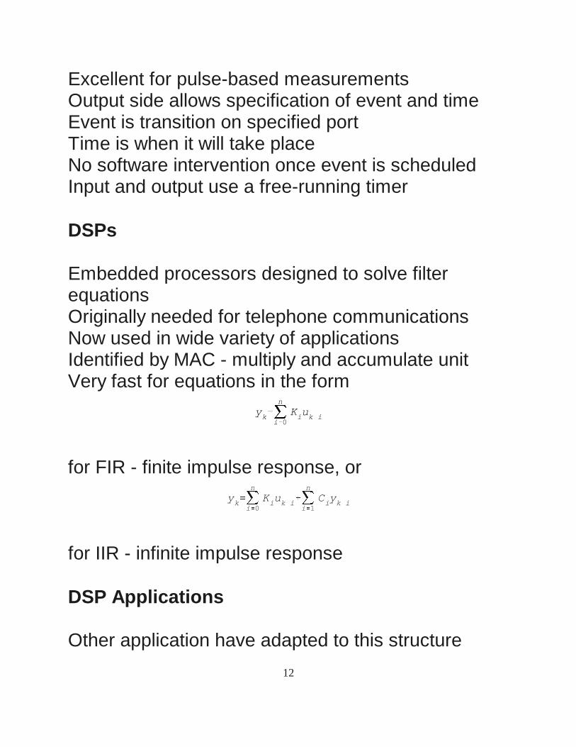
Excellent for pulse-based measurementsOutput side allows specification of event and timeEvent is transition on specified portTime is when it will take placeNo software intervention once event is scheduledInput and output use a free-running timer DSPs
Embedded processors designed to solve filterequationsOriginally needed for telephone communicationsNow used in wide variety of applicationsIdentified by MAC - multiply and accumulate unitVery fast for equations in the form
for FIR - finite impulse response, or
for IIR - infinite impulse response DSP Applications
Other application have adapted to this structure

13
Feedback control, for example, fits this modelOriginal DSPs were all integer (fixed point)Scaling a big part of designNewest have floating point RISC and Floating Point
Reduced instruction set computers (RISC)Simple internal structureMany registersSingle cycle instructionsLoad-store only,I.e., operations on registers only, no directoperations on memoryWhat to do with extra space on chip?-Memory management -Floating pointAdapted to embedded use because of floating pointspeedExample - printer controllers Embedded PCs
Widely known and available architectureDevelopment andprototyping can be done with anyPCMiniaturization is driven by portable market

14
Embedded systems can take advantage of this Software Development for Embedded Computers
Most require "cross" assemblers and compilersVery low cost products need assembly languageMeans of debugging is necessaryIn-circuit emulators (ICE)Used for "circuit-like" applicationsEmbedded computer has no hooks at all to outsideworldOther means use networks, serial connections, etc. Digital Logic
Information - coded into signal’s valueAnalog/digitalAnalog precision based on noise and
instrument’s resolving powerInformation measure - number of decisions that
could be carriedThat is, number of potential statesQuantized signals - minimize noise effects by
making quantization level bigger than noiseBinary - ultimate quantizationInformation based on signal value and buffer
zone

15
Example:value is 0 if signal < v1value is 1 if signal > v1 + vbufvalue is undefined in middle
Undefined means that logic elements could giveeither result
All modern digital cicuitry is binary (contrastmechanical calculators - digital base-10)
Protection Zone
Even the buffer specification is subject to noiseA signal near the boundary could be pushed into
the undefined regionTo protect against that, input and output have
separate specsFor 0, (max output) < (max input)For 1, (min output) > (min input)Example: TTL standard (nominal 0 - 5 volts)
Output: 0 < 0.4 volts, 1 > 2.4 voltsInput: 0 < 0.8 volts, 1 > 2 volts
0.4 volts is the protection zone Static/Dynamic, Algebra/Calculus
Follow same spirit as general dynamic systemsStatic system: outputs depends only on inputs

16
Dynamic system: outputs depend on inputs andhistory
For digital (binary) systems,Boolean algebra describes static behaviorSequential logic describes dynamic behavior
Boolean algebra well developed mathematicallySequential logic more ad hoc
Goals
Means of describing desired behavior of logicsystems, static and dynamicMethods for translation of description to
mathematically rigorous formGeneration of solution in logic formOptimization methods to minimize required
number of logic elementsTests for potential system problems (hazards)Implementation mechanisms
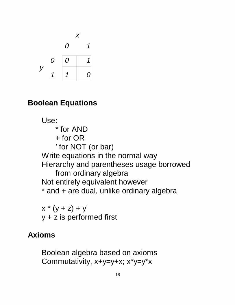
Boolean Algebra
George Boole (English mathematician, 1815-1864)
Symbol associated with binary value - 0/1,TRUE/FALSE, ON/OFF ...
x = 0; x = 1

x
17
x x’
0 11 0
xy x AND y x OR y
00 0 001 0 110 0 111 1 1
Note that variables have only two values --computer "words" are made from a set ofBoolean variables
NOT - unary operator, uses prime, x’, or bar,
Truth table, exhaustive explication of result
AND/OR
Standard logic definitions,
Alternate form for truth table, as a map; this is theexclusive-OR (XOR) operator:
0 1
0
1
0 1
1 0
x
y
18
Boolean Equations
Use:* for AND+ for OR’ for NOT (or bar)
Write equations in the normal wayHierarchy and parentheses usage borrowed
from ordinary algebraNot entirely equivalent however* and + are dual, unlike ordinary algebra
x * (y + z) + y’y + z is performed first
Axioms
Boolean algebra based on axiomsCommutativity, x+y=y+x; x*y=y*x
19
Associativity, (x+y)+z=x+(y+z); (x*y)*z=x*(y*z)Distributivity, x+(y*z)=(x+y)*(x+z);
x*(y+z)=(x*y)+(x*z)Note first relation above!Existence of 0,1, x+0=x; x*1=xExistence of complements, x+x’=1; x*x’=0
Theorems
A number of interesting theorems give mainmanipulation power to Boolean algebra
They will be used for logic circuit designThey can be proved either by reference to the
axioms (as in ordinary algebra), or byexhaustive substitution
Idempotent operators, x+x=x; x*x=xAbsorption, x+x*y=x; x*(x+y)=xSimplification, x+x’y=x+y; x*(x’+y)=x*yDeMorgan’s laws, (x+y)’=x’*y’; (x*y)’=x’+y’
Logic System Design
Goal - functioning circuitHow? Use Boolean algebra to go from design
spec to implementable logic functionDesign problem that results in static (Boolean)
design:

20
x1 x2 L
0 0 00 1 11 0 01 1 0
binary inputsbinary outputsno history dependence
Example: electronic door lockLock has a set of buttonsTo enter, person must simultaneously press the
correct combination of buttonsInputs: button-in = 1, button-out = 0Output: lock actuator, 0 lock, 1 unlock (power fail
to lock) Truth Table for Door Lock
Two button lock
Even for this two-variable problem, trial-errorfunction generation is not realistic
Solution can be obtained directly from truth tableForm a sum-of-products function,
y=c1*x1*x2+c2*x1*x2’+c3*x1’*x2+c4*x1’*x2’

21
The four terms express all possible ANDcombinations of x1, x2, and theircomplements
The coefficients can be 0 or 1That is, terms are included or left out
Function from Truth Table
Match terms by calling unprimed variable 1,primed variable 0
Coefficient is 1 if matching term has output=1, 0otherwise
In this case, matching term is for x1=0, x2=1,x1’*x2
Since this is the only 1 in the truth table, result isL = x1’*x2
All Boolean design flows from this procedureIt allows arbitrary synthesis of logic functionsIs the Boolean equivalent of regression, but,
it is exact! Complementary Forms
Unlike ordinary algebra, Boolean algebra iscompletely dual
This means that --0 and 1 have no specific significance and

22
can be exchanged arbitrarily* and + are also interchangeableparentheses and hierarchy are artificial and
do not represent andy mathematicalsignificance
Contrast these with ordinary algebra --0 has special significancemultiplication is fundamentally different than
additionThis means that the design procedure has a
complementary expression Product of Sums
The complementary form to the sum-of-productsis(x1+x2)*(x1’+x2)* ...
The rules are exact duals of the rules toconstruct the sum-of-products,
Each truth table entry that has a 0 outputgenerates an output term
Within each term, write variables with 0 inputsunprimed and variables with 1 primed
For the two button door lock:L = (x1+x2)*(x1’+x2)*(x1’+x2’)
Note that this is considerably more complex thanthe other form

23
Complexity is problem dependentFor example, consider the case where L=0
unlocks the doorFunction minimization can be done algebraically,
but rarely is in practice Minimization
Graphical map-based minimizationBased on repeated application of
xy + xy’ = xThat is, if two terms are identical, except that
one variable appears primed in one andunprimed in the other, that variable can beremoved
Graphical method - contstruct a table so thatadjacent cells follow this pattern
Then pairs of adjacent cells can be combined ...and pairs of pairs, etc.
Adjacency requires that only one variablechange between adjoining cells
OK for 2-variable map,

24
Combining Cells
Imagine a door lock with two possiblecombinations (one for building operator?)
This has two 1s so solution from truth tablewould be:x1’*x2’+x1*x2’
Above theorem shows that this can be reducedtox2’
Map shows same thingAdjacent 1s are collectedKeep only terms that don’t change for final
expression NonReducible Maps
Alternate combinations --
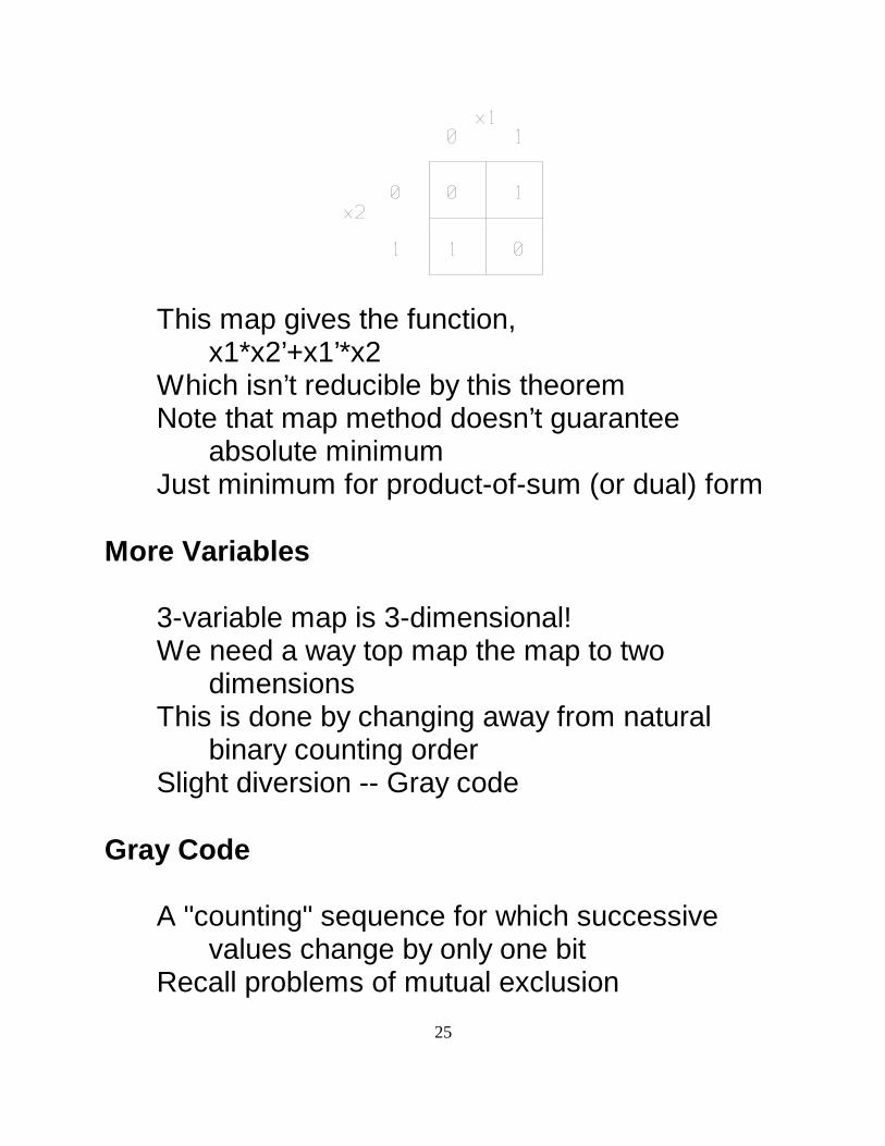
25
This map gives the function,x1*x2’+x1’*x2
Which isn’t reducible by this theoremNote that map method doesn’t guarantee
absolute minimumJust minimum for product-of-sum (or dual) form
More Variables
3-variable map is 3-dimensional!We need a way top map the map to two
dimensionsThis is done by changing away from natural
binary counting orderSlight diversion -- Gray code
Gray Code
A "counting" sequence for which successivevalues change by only one bit
Recall problems of mutual exclusion

26
Multi-bit changes cause problems if interruptedwhile changing
This is because multiple bits are changingsimultanwously
00 01 10 11Two of these transitions change both bitsAlternate counting order:00 01 11 10All one-bit changes!
Reflected Gray Code
This code is constructed by reflectionStart with 1-bit, 0 1To go to 2-bit, write first 2 numbers with leading
0,00 01 Get next 2 numbers by reversing the 1-bit
sequence, then putting on a leading 1,11 10, or 00 01 11 10To get 3-bit, do this again,000 001 011 010 (2-bit sequence + leading 0),
then,110 111 101 100, for000 001 011 010 110 111 101 100
Asynchronous Inputs
27
If Gray code is used, input signal can be readwith no synchronizer
Input must go through all intermediate values toget from one value to another
Reading at any time will give valid resultIf value is changing, result will be either new or
old value; never a spurious valueFor non-Gray code inputs, a synchronizer (clock)
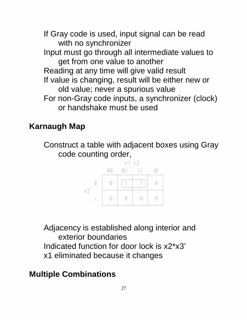
or handshake must be used Karnaugh Map
Construct a table with adjacent boxes using Graycode counting order,
Adjacency is established along interior andexterior boundaries
Indicated function for door lock is x2*x3’x1 eliminated because it changes
Multiple Combinations

28
Adjacent pairs of pairs can be eliminated in asingle step
In this case, both x1 and x3 change inside thebox, so the result is,x2
This can be extended to 4 variables,
This gives,x1’*x3’*x4+x2*x3’+x1*x3*x4’This can be extended all the way to 6 variables
by using multiple tables
29
Beyond 6, other methods for minimization mustbe used
Don’t Care
Some input conditions are considered"impossible"
The circuit input, however, will always have avalue
These combinations can trigger error trapsOr, they can be used to further minimize the
systemCarefully setting don’t-care cells to 0 or 1 can
increase the size of groupings Hazards
GlitchesShort, spurious signals generated when inputs
are changingConsider the following map,

30
The function for this map is,x1’*x3’*x4+x2*x3’+x1*x3*x4During an input change from 1101 to 1111, the
output remains at 1The first term is 0 for bothThe 2nd term uses x3’ while the 3rd uses x3In general, x3 and x3’ will not change
simultaneouslyThis can cause a glitch (hazard)
Glitch Dangers and Remedy
If device connected to output is static, usually noproblem
Low pass filter (like motor) will ignore short glitchIf device is dynamic (sequential), however, it
might respondFor example, a counter

31
Remedy:Add additional term covering the transitionThat is, all transitions between adjacent boxes
should take place under a common termThat term will not change value during the
transition, so will keep output constant De-Glitchified (?) System
Karnaugh map with added term:
Function now is:x1’*x3’*x4+x2*x3’+x1*x3*x4+x1*x2*x4The last term is 1 throughout the troubling
transitionAll transitions in this map are now protected
against static hazards

32
Physical Realization of Boolean Functions
Combinational logic -- static, BooleanBecause of digital quantization, relatively easy to
achieveCircuit is "almost exact" representation of
mathematicsReal circuit has some delayDelay has no serious consequence for
combinational systemsVery important when combinational system
becomes part of a sequential system Relay Logic
Relay logicSolenoid and contactLogic function defined as continuityFor example, closed --> 1Relays can be normally open or normally closedParallel and series combinations give any logic
functionRelays no longer used for large scale logicStill used for low-impedance switching (e.g.,
thermocouple) and high power switching Programmable Logic Controllers (PLC)

33
Replaced relays and electronic logic (where theelectronic logic was being used to replacerelays)
Ruggedized construction, isolated input/outputLadder diagram (relay logic) for programmingFunction is now completely reproducible by
microcomputersHowever, PLCs remain in market because they
fit many applications very well Conventions
0, 1 are dualNo mathematical preference for connection to
physical signalRelay - as above, closed = 1, open = 0Normally open relays can be cascaded with no
"sign" changeUse normally closed relay to generate
complementElectrical - high voltage = 1, low voltage = 0However, reverse conventions are possibleMathematics is the sameMixed conventions can be used in the same
system!Can lead to more efficient circuit
34
Fluid Logic
Hydraulic or pneumaticMixed or pure domainValves act much like relaysFluidic components have no moving partsUse wall attachment, vorticity to generate
switching functionsFluidics had very high profile in 60sSettled down to niche productFluid logic important in electrically adverse
environmentsExplosive, jet engines, ...
Electronic Logic
Diode logic, passive circuitsLimited cascade ability - amplifiers neededRTL (resistor-transistor logic), includes the
amplifierAmplifier causes inversion of logic functionNAND, or NOR Too slow, uses too much power
TTL, CMOS
Transistor, transistor logic, TTL

35
Most common family of discrete logiccomponents
Several variants available based on speed orpower consumption
0 - 5 volts nominalTypically available as input or output to computer
digital portsComplementary metal oxide semiconductors
(CMOS)Often used for more highly integrated
componentsSimilar voltage range to TTLEasily interfaced to TTLLow power consumption, especially when
quiescentVery sensitive to static electricity
Pseudo Circuits
First step in circuit designConvert Boolean equations into logic block
diagramsThese are very close to actual circuit elementsStandard symbols:

36
NAND is (x*y*...)’NOR is (x+y+...)’They are important because that is how many
real elements work Door Latch in Circuit Form
Take earlier solution,L = x1’ * x2Convert to pseudo-circuit elements,
Conversion to NAND/NOR Form
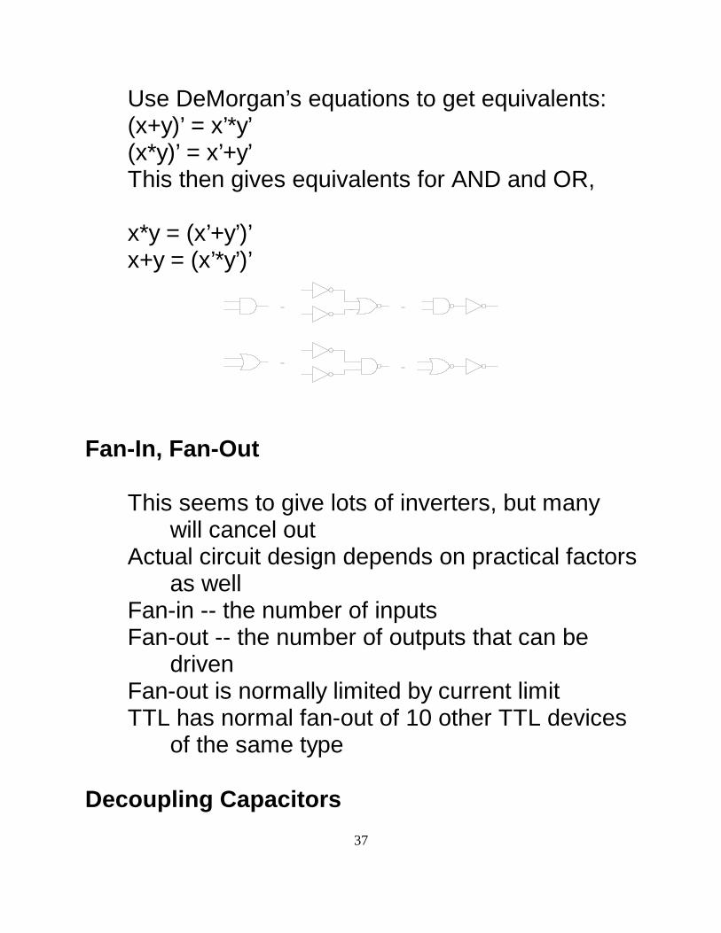
37
Use DeMorgan’s equations to get equivalents:(x+y)’ = x’*y’(x*y)’ = x’+y’This then gives equivalents for AND and OR,
x*y = (x’+y’)’x+y = (x’*y’)’
Fan-In, Fan-Out
This seems to give lots of inverters, but manywill cancel out
Actual circuit design depends on practical factorsas well
Fan-in -- the number of inputsFan-out -- the number of outputs that can be
drivenFan-out is normally limited by current limitTTL has normal fan-out of 10 other TTL devices
of the same type Decoupling Capacitors

38
As components operate, their need for currentvaries
These transients can cause componentinteraction through the power supply circuitry
Capacitors at power input to each activecomponent provide local power to meettransient needs
General rule -- decoupling capacitor for each IC,0.01 - 0.1 microfarad
It is possible to use fewer, but this rule is safe Open Collector Output
The output transistor acts as a switchOutput is connected to ground or left openTo convert this to a voltage, a "pull-up" resistor is
usedThe pull-up resistor is installed from the output to
a 5v sourceIf a device does not have an internal pull-up, it is
called open collectorIn that case, an external pull-up must be
supplied (of order 1KOhm)Small pull-up for high-speed, high power drain

39
Bus Connections
Early application of open collectorSeveral devices connected to a single set of
wiresMinimizes wiring in computer/data connectionsAllows device interchange easilyProblem: if several devices try to put information
on a wire at the same time, a conflict willresult
Result is indeterminateOpen collector allows an output wire to be
sharedAs long as switch is open (no pull-up) there is no
loadAny device that closes its switch determines the
state of that bus wire

40
A single pull-up is provided for the wire Three State Outputs
Alternative to open collector for driving a busUses an actual switching element to disconnectOpen collector elements are noise immune
because of interactions with parasiticcapacitance in the bus wiring
Three state has fewer noise, speed problemsMore complex circuitSeparate "enable" input is used to determine
whether output is at high or low impedancestate
Note -- three state does not mean three logicstates!
Tri-state logic is Nat’l Semiconductor trade name Wired AND/OR
Open collector can be used to get a "freebie"Depending on logic convention, a free AND or
OR gate can be constructedWire open collector outputs togetherDifficult to debug because individual input values
cannot be measuredOpen collector can also be used to drive load of

41
different voltage rangeBut, beware of breakdown voltage for the device
Schmidt Trigger
Analog-digital conversion1-bit"Converter" is switching deviceSharp switching boundary can cause multipleswitches if there is any oscillation in the analogsignal
Hysteretic Boundary
Schmidt trigger uses boundary defined withhysterisis
Minimizes switching transients

42
Programmable Logic Devices (PLDs)
Integrated circuits can have 100s of thousandsof elements on a chip
TTL components only require a few transistorseach
TTL circuits of any size are extremely inefficientwith respect to run-of-the-mill ICs!
Direct integration isn’t practicalToo many external pins required to just put lots
of gates (AND, OR, NAND, etc.) on a chipExternal pin requirements are a major design
constraint in IC designMost circuits have a limited number of inputs and
outputs
43
Application-specific ICs (ASICs) can be made forhigh volume use
Very expensiveHighly integrated logic replacement devices use
internal interconnects to allow arbitraryfunctions
Field programmability critical element for generalusage
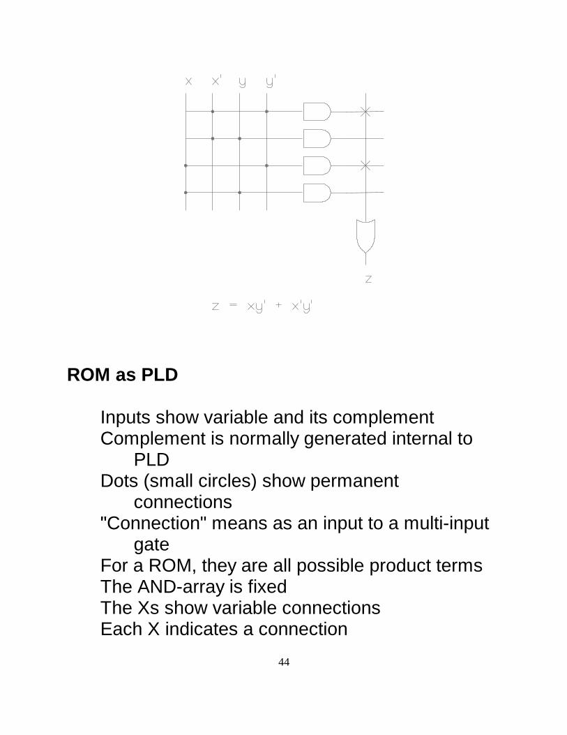
ROM As Logic Device
Address lines inOne or more outputs, depending on organizationEach address can have a unique outputROMs can be field programmed, field erasedLooks like truth tableCan be viewed as sum-of-products with no
minimizationFigure below shows PLD format of PROMDiagram shows logical connectionsIt is not a circuit diagram
44
ROM as PLD
Inputs show variable and its complementComplement is normally generated internal to
PLDDots (small circles) show permanent
connections""Connection" means as an input to a multi-input
gateFor a ROM, they are all possible product termsThe AND-array is fixedThe Xs show variable connectionsEach X indicates a connection

45
The OR array is programmableFor the function
z=x*y’+x’*y’The Xs are marked for each of these terms for
connection to the output ORFor this 2-input, 1-output device, any possible
output function can be generated PAL -- Programmable AND, Fixed OR
Programmable Array LogicPAL is a tradename of Monolithic Memories
(since purchased by AMD)This inversion of function makes general logic
implementation much more effectiveExample,
z1=x2*x4+x1*x3
z2=x2’*x3*x4+x1’*x2*x3*x4’+x1*x2*x3’+x1*x4

46
Note that the bottom two rows have all XsThis is the unprogrammed state and has no
effect on the result PLA -- Both Programmable
Programmable Logic Array (unfortunate set ofnames!)
Adds more logic efficiency at expense of moreinternal complication
And more pinsWith programmable OR array also, the AND
rows can be assigned to any of the outputs

47
Same example, the bottom two rows could beassigned to a third output, if one existed,
The extra two rows are now connected to z3 andcan be programmed
PLA architecture allows for more functions perchip
EPLDs
Programmability has opened the marketimmensely
Device architectures have array logic at coreSurround it with a variety of other elements
48
Greater functionality to allow complete systemson one chip
Array logic is broken down into "macro cells"Recognizes that individual logic functions, or
sets of functions, are usually modest in size Programming EPLDs
Can be programmed as aboveSoftware usually usedWe have software from IntelGeneral procedure:
name inputs and outputsspecify part to be usedspecify input and output connection typesspecify Boolean equations
Program will simplify the expression, produceprogramming information for the PLD
Second program can download information toPLD for programming
Example
z1=x2*x4+x1*x3
z2=x2’*x3*x4+x1’*x2*x3*x4’+x1*x2*x3’+x1*x4

49
Also, to show reduction ability, add the equation
L = (x5+x6)*(x5’+x6)*(x5’+x6’)
Note that this equation is not in sum-of-productsform
Program will convert it to that form and simplify it Logic Optimizing Compiler (LOC) Input
YOUR NAMEYOUR COMPANYDATAU10015AC312PACKAGE: D5AC312-25OPTIONS: TURBO=ONPART: 5AC312
INPUTS: x1,x2,x3,x4,x5,x6
OUTPUTS: z1,z2,L
NETWORK:x1 = INP(x1)x2 = INP(x2)

50
x3 = INP(x3)x4 = INP(x4)x5 = INP(x5)x6 = INP(x6)z1 = CONF(z1,vcc)z2 = CONF(z2,vcc)L = CONF(L,vcc)
EQUATIONS:
z1 = x2*x4+x1*x3; z2= x2’*x3*x4+x1’*x2*x3*x4’+x1*x2*x3’+x1*x4; L = (x5+x6)*(x5’+x6)*(x5’+x6’);
END$ LOC Output
Optimized equations:
EQUATIONS:L = x5’ * x6;
z2 = x2 * x3 * x4’ * x1’ + x2 * x3’ * x1 + x2’ * x3 * x4 + x4 * x1;
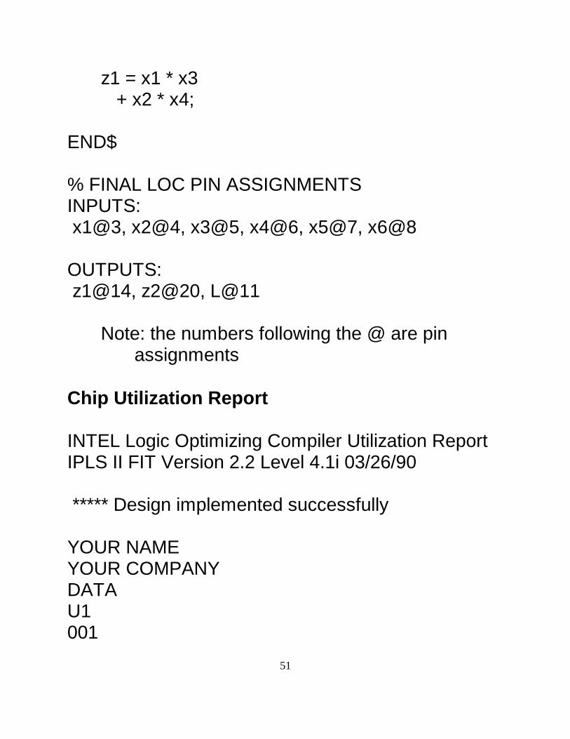
51
z1 = x1 * x3 + x2 * x4;
END$
% FINAL LOC PIN ASSIGNMENTSINPUTS: x1@3, x2@4, x3@5, x4@6, x5@7, x6@8
OUTPUTS: z1@14, z2@20, L@11
Note: the numbers following the @ are pinassignments
Chip Utilization Report
INTEL Logic Optimizing Compiler Utilization ReportIPLS II FIT Version 2.2 Level 4.1i 03/26/90
***** Design implemented successfully
YOUR NAMEYOUR COMPANYDATAU1001

52
5AC312PACKAGE: D5AC312-25OPTIONS: TURBO=ON
5AC312 - - - - - Gnd -| 1 24|- Vcc Gnd -| 2 23|- Gnd x1 -| 3 22|- Gnd x2 -| 4 21|- Gnd x3 -| 5 20|- z2 x4 -| 6 19|- Gnd x5 -| 7 18|- Gnd x6 -| 8 17|- Gnd Gnd -| 9 16|- Gnd Gnd -|10 15|- Gnd L -|11 14|- z1 GND -|12 13|- Gnd - - - - -
**OUTPUTS**
Name Pin Resource MCell PTerms | SyncClock
z1 14 CONF 2 2/16 | - z2 20 CONF 7 4/16 | -

53
L 11 CONF 1 1/12 | -
**INPUTS**
Name Pin Resource MCell PTerms | SyncClock
x1 3 INP - - | - x2 4 INP - - | - x3 5 INP - - | - x4 6 INP - - | - x5 7 INP - - | - x6 8 INP - - | -
**UNUSED RESOURCES**
Name Pin Resource MCell PTerms
- 1 INPUT - - - 2 MCELL 11 16 - 9 INPUT - - - 10 INPUT - - - 13 INPUT - - - 15 MCELL 3 16 - 16 MCELL 4 16
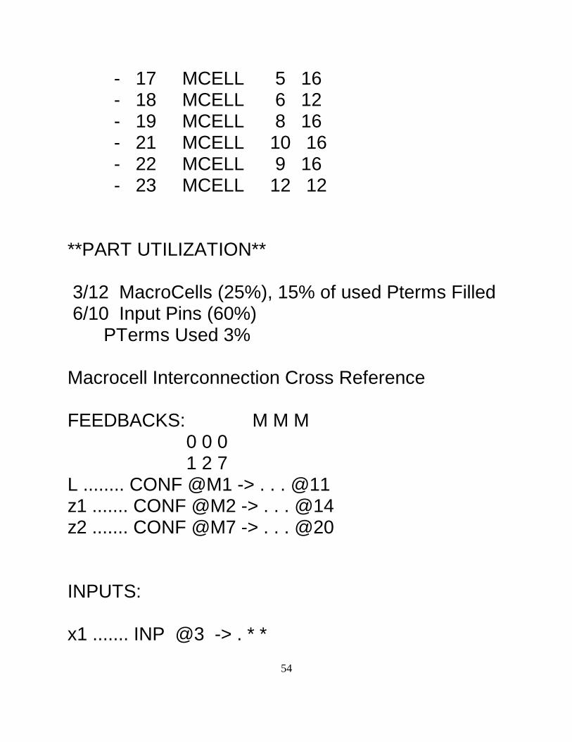
54
- 17 MCELL 5 16 - 18 MCELL 6 12 - 19 MCELL 8 16 - 21 MCELL 10 16 - 22 MCELL 9 16 - 23 MCELL 12 12
**PART UTILIZATION**
3/12 MacroCells (25%), 15% of used Pterms Filled 6/10 Input Pins (60%) PTerms Used 3%
Macrocell Interconnection Cross Reference
FEEDBACKS: M M M 0 0 0 1 2 7 L ........ CONF @M1 -> . . . @11z1 ....... CONF @M2 -> . . . @14z2 ....... CONF @M7 -> . . . @20
INPUTS:
x1 ....... INP @3 -> . * *

55
x2 ....... INP @4 -> . * *x3 ....... INP @5 -> . * *x4 ....... INP @6 -> . * *x5 ....... INP @7 -> * . .x6 ....... INP @8 -> * . . L z z 1 2 . = not connected x = no connection possible* = signal feeds cell ? = error, unable to fit Macro Cells
Internal partition of chipUsed to make efficient use of chip for lots of
small equationsMacro cells allow some interconnectGive some of the function of PLA but with less
complexityChip is otherwise equivalent of PALMany ways of connecting outputs are allowedThis design gives a purely Boolean outputWe will see more in sequential logic use of these
chips Sequential Logic

56
Output depends on current and past inputsHistory dependence is achieved with feedbackGeneral model for sequential circuit:
Flip-Flop
A number of memory element are possible,including pure processing delay
Explicit memory elements make circuit designeasier
Set-reset (SR) flip-flop is very common andsimple
It is a sequential circuit itself
A simple program can simulate its behavior:

57
#include <stdio.h>
#define NSR 14static int ss[] = {0,1,1,1,0,0,0,0,0,0,0,1,1,1};static int rr[] = {0,0,0,0,0,0,1,1,1,0,0,1,1,1};static int n = 13;
main(ac,av)int ac;char *av[];{int s,r,q = 0,qp = 1,nxt_q,nxt_qp,i;
printf("s r q qp nq nqp\n");
for(i = 0; i < n; i++){if(i >= NSR)
{s = ss[NSR - 1];r = rr[NSR - 1];}
else{s = ss[i];r = rr[i];

58
}
nxt_q = !(qp || r);nxt_qp = !(q || s);printf("%d %d %d %d %d
%d\n",s,r,q,qp,nxt_q,nxt_qp);q = nxt_q;qp = nxt_qp;}
} Results
s r q qp nq nqp0 0 0 1 0 11 0 0 1 0 01 0 0 0 1 01 0 1 0 1 00 0 1 0 1 00 0 1 0 1 00 1 1 0 0 00 1 0 0 0 10 1 0 1 0 10 0 0 1 0 10 0 0 1 0 11 1 0 1 0 01 1 0 0 0 0

59
SR Definition
The two outputs are complementsSR should never be 11When S=1, Q->1When SR = 00, Q doesn’t changeWhen R=1, Q->0
Example: Door Lock
New design, use sequence for combinationE.g, press and release button 1, then press and
release button 2Two buttons give lots more combinations when
used in sequence
Circuit Design
Brute force design using SR flipflopsIdentify each unique situation

60
Call it a stateUse a flip flop to record that the state has been
enteredCascade flip flop output to next flip flopStates can only be excited in sequenceGeneral system design --
Excitation Design
Excitation circuitry is BooleanDescribe conditions needed for each stateFor first flipflop to turn on, for examplex1=1, x2=0, Q1=0, i.e.,User has pressed first key, second key is up,
first flipflop is offThis gives the following set of equations:

61
s1=x1*x2’*q1’s2=x1’*x2’*q1s3=x1’*x2*q2s4=x1’*x2’*q3
Output equation:L = q4
Note that R inputs can be used as master reset Simulation
#include <stdio.h>
#define NX 11static int xx1[] = {0,1,1,1,1,1,1,0,0,0,0};static int xx2[] = {0,0,0,0,0,0,1,1,1,0,0};
int sr(int s,int r,int q) /* Return next value for srflipflop output------------------------ */{int next;
if(s && r){printf("Illegal SR FLipflop state\n");exit(1);}

62
if(s)next = 1;else if(r)next = 0;else next = q;return(next);}
main(){int x1,x2,L;int s1,s2,s3,s4;int r1 = 0,r2 = 0,r3 = 0,r4 = 0;int q1 = 0,q2 = 0,q3 = 0,q4 = 0;int nq1,nq2,nq3,nq4;int i,n = 13;
printf("x s q next-q L\n");
for(i = 0; i < n; i++){if(i >= NX)
{x1 = xx1[NX - 1];x2 = xx2[NX - 1];}
else{x1 = xx1[i];

63
x2 = xx2[i];}
s1 = x1 && !x2 && !q1;s2 = !x1 && !x2 && q1;s3 = !x1 && x2 && q2;s4 = !x1 && !x2 && q3;L = q4;nq1 = sr(s1,r1,q1);nq2 = sr(s2,r2,q2);nq3 = sr(s3,r3,q3);nq4 = sr(s4,r4,q4);printf("%d %d %d %d %d %d %d %d %d %d
%d %d %d %d %d\n",
x1,x2,s1,s2,s3,s4,q1,q2,q3,q4,nq1,nq2,nq3,nq4,L);q1 = nq1;q2 = nq2;q3 = nq3;q4 = nq4;}
} Results

64
x s q next-q L0 0 0 0 0 0 0 0 0 0 0 0 0 0 01 0 1 0 0 0 0 0 0 0 1 0 0 0 01 0 0 0 0 0 1 0 0 0 1 0 0 0 00 0 0 1 0 0 1 0 0 0 1 1 0 0 00 0 0 1 0 0 1 1 0 0 1 1 0 0 00 0 0 1 0 0 1 1 0 0 1 1 0 0 00 1 0 0 1 0 1 1 0 0 1 1 1 0 00 1 0 0 1 0 1 1 1 0 1 1 1 0 00 1 0 0 1 0 1 1 1 0 1 1 1 0 00 0 0 1 0 1 1 1 1 0 1 1 1 1 00 0 0 1 0 1 1 1 1 1 1 1 1 1 10 0 0 1 0 1 1 1 1 1 1 1 1 1 10 0 0 1 0 1 1 1 1 1 1 1 1 1 1

65
x s q next-q L0 0 0 0 0 0 0 0 0 0 0 0 0 0 01 0 1 0 0 0 0 0 0 0 1 0 0 0 01 0 0 0 0 0 1 0 0 0 1 0 0 0 01 0 0 0 0 0 1 0 0 0 1 0 0 0 01 0 0 0 0 0 1 0 0 0 1 0 0 0 01 0 0 0 0 0 1 0 0 0 1 0 0 0 01 1 0 0 0 0 1 0 0 0 1 0 0 0 00 1 0 0 0 0 1 0 0 0 1 0 0 0 00 1 0 0 0 0 1 0 0 0 1 0 0 0 00 0 0 1 0 0 1 0 0 0 1 1 0 0 00 0 0 1 0 0 1 1 0 0 1 1 0 0 00 0 0 1 0 0 1 1 0 0 1 1 0 0 00 0 0 1 0 0 1 1 0 0 1 1 0 0 0 But, Will it Work?
Probably...This design is asynchronousCircuit elements change as soon as they canDesign is straightforward, not much place for
problemsWith cascaded flipflops, timing is not very
importantNo method to the designNo way of minimizingNo way to check for hazards

66
Timing problems can arise if signals areexposed to different amounts or delay ontheir way to memory elements
More complex problems can defy ad hoc design Synchronous Systems
All logic is synchronized with a clockThis provides the same noise margin in the
temporal domain that binary quantizationprovides in the signal domain
Memory elements are constrained to switch onlyin synchrony with the clock
Timing constraints are local to each memoryelement
All input circuitry must be stable before memoryelements change
Asynchronous inputs should be passed throughsynchronizers
Design starts with a state transition diagramThis is the connection to engineering problem
descriptions State Transition Logic
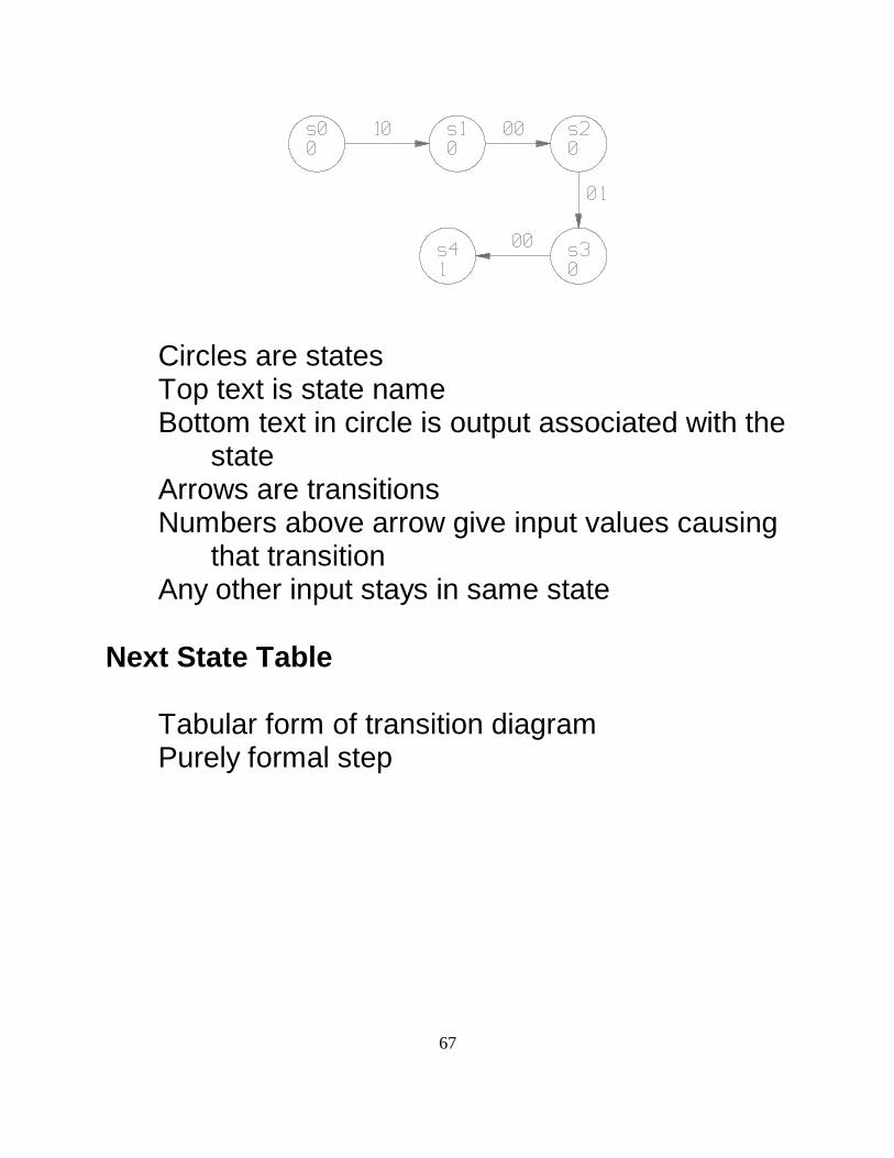
67
Circles are statesTop text is state nameBottom text in circle is output associated with the
stateArrows are transitionsNumbers above arrow give input values causing
that transitionAny other input stays in same state
Next State Table
Tabular form of transition diagramPurely formal step

log2n
68
Next State Table:
Inputs, x1 x2
CurrentState
00 01 11 10
S0 S0 S0 S0 S1
S1 S2 S1 S1 S1
S2 S2 S3 S2 S2
S3 S4 S3 S3 S3
S4 S4 S4 S4 S4
State Assignment
Number of states, at least , where n is the
number of statesIn this case, three state variablesSome minimization might be possibleWe will deal with that laterSynchronous circuits are not very sensitive to
state assignmentUse gray code sequence...S0 000S1 001S2 011

69
S3 010S4 110
Memory Element
In synchronous circuits the memory elementmust be clocked
Excitation circuitry must settle before memorychanges
In order to avoid oscillation, devices are normallyedge-triggered
Output changes on arrival of clock transitionEasiest to design with is D-flipflopIt passes input to output on clock transitionIts next-state description is simply,
Q+ = QTo design with a D flipflop, the next state
diagram is combined with the stateassignment to produce excitation equations
Door Lock Excitation Equations

70
Next State Table, q1+,q2+,q3+
Inputs, x1x2
CurrentState,q1,q2,q3
00
01
11
10
000
000
000
000
001
001
011
001
001
001
011
011
010
011
011
010
110
010
010
010
110
110
110
110
110
Excitation equations or maps can be writtendirectly from this table

71
This gives the excitation equation for q1+ as,q1+ = x1’*x2’*q2*q3’+q1(By making the don’t cares 1)Maps for q2+ and q3+ are:
q2+ = x1’*x2’*q3+q2+q1

72
q3+ = x1*x2’*q2’+x1*q3+q2’*q3+x1’*x2’*q3
Output equation: output is on only for state 4, s4= 110L = q1*q2*q3’
Simulation
/* Sequential door lock using D-flipflops */
#include <stdio.h>
#define NX 11static int xx1[] = {0,1,1,1,0,0,0,0,0,0,0};static int xx2[] = {0,0,0,0,0,0,1,1,1,0,0};...
/* Excitation equations */
nq1 = (!x1 && !x2 && q2 && !q3) || q1;nq2 = (!x1 && !x2 && q3) || q2 || q1;nq3 = (x1 && !x2 && !q2) || (x1 && q3) || (!q2 &&
q3) || (!x1 && !x2 && q3);
L = q1 && q2 && !q3;printf("%d %d %d %d %d %d %d %d %d\n",x1,x2,q1,q2,q3,nq1,nq2,nq3,L);

73
q1 = nq1;q2 = nq2;q3 = nq3;}
} Results
x q next-q L0 0 0 0 0 0 0 0 01 0 0 0 0 0 0 1 01 0 0 0 1 0 0 1 01 0 0 0 1 0 0 1 00 0 0 0 1 0 1 1 00 0 0 1 1 0 1 1 00 1 0 1 1 0 1 0 00 1 0 1 0 0 1 0 00 1 0 1 0 0 1 0 00 0 0 1 0 1 1 0 00 0 1 1 0 1 1 0 10 0 1 1 0 1 1 0 10 0 1 1 0 1 1 0 1 Will it Work?
This will almost certainly workThe design is consistent and can be checked

74
Because of the clock there are no timingproblems
The only timing constraint is that the clockshould not be too fast
For standard logic devices, max speed is about50-100 MHz
This design is not complete, howeverNo way to resetEither after successful or unsuccessful attemptUnsuccessful entries should probably cause
restartStart light is probably needed to avoid user
confusion Other Memory Elements
Other clocked flipflopsT (toggle), JK can be clockedToggle changes state if input is 1JK acts as SR plus toggle ..Sets when J=1, resets when K=1, toggles when
both inputs=1It is generally considered that T of JK will give
smaller circuits than DExcitation maps are still based on next state
tableLatch/memory/flip-flop:
75
Latch: clocked element, input directlyconnected to output (output can changewhen input changes)
Flip flop: output only changes when clockchanges
Memory or register: clocked D flip flop Master-Slave, Edge Triggered Flip Flops
Master-slave flip flop is two stage deviceSecond stage operates off inverted clockInput goes through in a two-set processThis prevents Input from directly affecting outputNot commonly used for new designsEdge-triggered flip flopOutput changes on clock transition (up or down)Most common for current designsMore complicated internally
Excitation for T Flipflop
Excitation input = 1 if next state is different frompresent state, = 0 if it is the same
Next state table for door (repeated from above):

76
Next State Table, q1+,q2+,q3+
Inputs, x1 x2
CurrentState,q1,q2,q3
00 01 11 10
000 000 000 000 001
001 011 001 001 001
011 011 010 011 011
010 110 010 010 010
110 110 110 110 110
Q2 Excitation Map
Note that the other toggle input maps also haveonly one entry each
Using EPLDs for State Machines

77
PLDs contain memory elements and feedbackpaths internal to the chip
This allows for complete implementation of statemachines on a single PLD
We will use 85C220 and 85C224These have built in D (register) flip flopsSoftware from Intel allows direct input of state
machine descriptionDesign is automatic from thereResult can also be simulated
State Machine Input for Door Lock
YOUR NAMEYOUR COMPANYDATE1A85C224LOCK2: Door Lock
OPTIONS: TURBO = OFFPART: 85C224INPUTS:
CLKx1x2
OUTPUTS:LQ1 % This state variable will appear as an output

78
--others will not %NETWORK:
L = CONF(L,VCC)
EQUATIONS:
L = Q1 * Q2 * Q3’;
MACHINE: LOCK2CLOCK: CLKSTATES: [ Q1 Q2 Q3] S0 [ 0 0 0]S1 [ 0 0 1]S2 [ 0 1 1]S3 [ 0 1 0]S4 [ 1 1 0]
S0:IF x1 * x2’ THEN S1
S1: IF x1’ * x2’ THEN S2
S2: IF x1’ * x2 THEN S3
S3: IF x1’ * x2’ THEN S4
S4:IF x1 * x2 THEN S0
% The state machine software will notallow a state with no transitions! This willgo back to start when both buttons are pressed %
END$

79
Logic Design for Lock
...NETWORK:CLK = INP(CLK)x1 = INP(x1)x2 = INP(x2)L = CONF(L,VCC)
%I/O’s for State Machine "LOCK2"%Q1, Q1 = RORF(Q1.d, CLK, GND, GND, VCC)Q2 = NORF(Q2.d, CLK, GND, GND)Q3 = NORF(Q3.d, CLK, GND, GND)
EQUATIONS:L = Q1 * Q2 * Q3’;
%Boolean Equations for State Machine "LOCK2"Current State Equations for "LOCK2"%S0 = Q1’*Q2’*Q3’;S1 = Q1’*Q2’*Q3;S2 = Q1’*Q2*Q3;S3 = Q1’*Q2*Q3’;S4 = Q1*Q2*Q3’;%SV Defining Equations for State Machine "LOCK2"%Q1.d = S4.n;Q2.d’ = S1.n

80
+ S0.n;Q3.d = S1.n + S2.n;%Next State Equations for State Machine "LOCK2"%S1.n = (S1 * (x1’ * x2’)’) + (S0 * (x1 * x2’));S0.n = (S4 * (x1 * x2)) + (S0 * (x1 * x2’)’);S2.n = (S2 * (x1’ * x2)’) + (S1 * (x1’ * x2’));S4.n = (S4 * (x1 * x2)’) + (S3 * (x1’ * x2’));
END$ Minimized Design
...EQUATIONS:
Q3.d = Q1’ * Q2’ * x1 * x2’ + Q1’ * Q3 * x2’ + Q1’ * Q2’ * Q3 + Q1’ * Q3 * x1;
Q2.d’ = Q1 * Q2 * Q3’ * x1 * x2 + Q1’ * Q2’ * Q3’ + Q1’ * Q2’ * x2 + Q1’ * Q2’ * x1;
Q1.d = Q2 * Q3’ * x1’ * x2’ + Q1 * Q2 * Q3’ * x2’
81
+ Q1 * Q2 * Q3’ * x1’;
L = Q1 * Q2 * Q3’;
END$ Same Problem Using T-Flip Flops
The same problem can be solved for a devicethat also has toggle flip flops (5AC312)
This is the minimized circuit:
EQUATIONS:Q3.t = Q1’ * Q2’ * Q3’ * x1 * x2’ + Q1’ * Q2 * Q3 * x1’ * x2;
Q2.t = Q1’ * Q2’ * Q3 * x1’ * x2’ + Q1 * Q2 * Q3’ * x1 * x2;
Q1.t = Q1’ * Q2 * Q3’ * x1’ * x2’ + Q1 * Q2 * Q3’ * x1 * x2;
L = Q1 * Q2 * Q3’;
Note that the excitation equations are muchsimpler
Simulation -- Is it Right?
The simulation program in the design package

82
takes an input "vector" and applies it to thedesign to simulate the output
The vector file:
;Vector file for LOCK2 simulation
000100010110000100000101001101000100000000 Results

83
C x x L Q Q Q L 1 2 1 2 3 K -0001- | | | | | | | -0002- ‘ -, | | | | | | -0003- ,-’ ‘ -, | | | | | -0004- ‘ -, | | | | | ‘ -, -0005- ,-’ ,-’ | | | | | -0006- ‘ -, | | | | ‘ -, | -0007- ,-’ | | | | | | -0008- ‘ -, | ‘ -, | | | | -0009- ,-’ | | | | | | -0010- ‘ -, | | | | | ,-’ -0011- ,-’ | ,-’ | | | | -0012- ‘ -, | | ‘ -, ‘ -, | | -0013- ,-’ | | | | | | -0014- | | | | | | | Asynchronous Inputs
Time of transition is not predictableCan come anywhere in the clock cycleIf input appears at several places in the circuit,
which is normal...Each will have different delays due to different
propogation pathsAt time of clock transition, the signal due to a
single input can have different values at

84
different placesCommon solution to this -- pass asynchronous
signal through a clocked D flip flopPropogate outut of D flip flop instead of actual
asynchronous signalSome PLDs have registered inputs for this
purposeOther problem -- metastabilityNo real solution. Problem is statisticalWill be discussed later
Moore/Mealy
Moore machine: outputs functions of state onlyMealy machine: outputs functions of state and
inputsMoore type systems are simpler to design and
more amenable to minimizationBy ANDing inputs with clock, Mealy machine can
be made to produce pulsed outputsIn transition diagrams, Moore outputs are
associated with states, Mealy outputs withstates and transitions
State Table Reduction
It might be possible to reduce the number of

85
rows in a state tableIf so, the complexity of state excitation and the
number of don’t cares in the excitation mapswill increase
In some cases, the number of state variablesmight decrease
Using PLD design, this might fit an otherwisetoo-big design into a PLD
It might allow extra state machines in the samePLD
Reduction Procedure
State table rows with different outputs cannot becombined
This eliminates most reduction in Mealymachines because output depends on inputalso so can be different for each column
First step is to construct an implication tableIt has states on each axisEach box will be used to determine if that state
pair is equivalentFor initial construction, mark X if the outputs of a
state pair don’t matchIf the outputs match, write the names of any
state pairs that are required for"equivalence"
86
Next State Table:
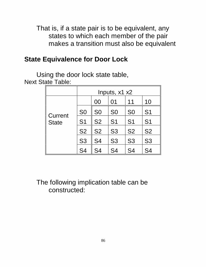
Inputs, x1 x2
CurrentState
00 01 11 10
S0 S0 S0 S0 S1
S1 S2 S1 S1 S1
S2 S2 S3 S2 S2
S3 S4 S3 S3 S3
S4 S4 S4 S4 S4
That is, if a state pair is to be equivalent, anystates to which each member of the pairmakes a transition must also be equivalent
State Equivalence for Door Lock
Using the door lock state table,
The following implication table can beconstructed:

87
Subsequent passes are generated by checkingthe equivalence pairs and Xing those thatwill no longer work (this example ends upwith no reduction possible)
Asynchronous Sequential Logic
No clockAll elements respond immediately to transitionsInternal circuit timing must be carefully controlledIn synchronous circuit input and memory
elements change don’t change at the sametime
Why?Stand-alone circuit doesn’t need a clock, lowers
costCan be faster (doesn’t have to wait for clock)
88
Synchronous memory elements (D, T, JK FFs)are themselves asynchronous circuits
Much less common than synchronous circuits Flow Tables
Because inputs are always connected, transientsmust be accounted for
Flow tables are similar to next-state tables ofsynchronous circuits
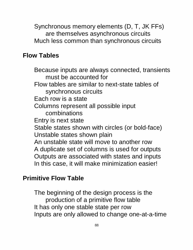
Each row is a stateColumns represent all possible input
combinationsEntry is next stateStable states shown with circles (or bold-face)Unstable states shown plainAn unstable state will move to another rowA duplicate set of columns is used for outputsOutputs are associated with states and inputsIn this case, it will make minimization easier!
Primitive Flow Table
The beginning of the design process is theproduction of a primitive flow table
It has only one stable state per rowInputs are only allowed to change one-at-a-time

89
SR OutputState 00 01 11 10 a a c - b 0 b d - - b 1 c a c - - 0 d d c - b 1
Circuit must be allowed to reach stable statebefore next input change
This is a "fundamental mode" circuitAlternate definition is "pulse mode", very similar
to synchronous in designInputs must be short pulses; short enough so
that the pulse is gone before any feedbacksignals arrive
Set-Reset Flip-Flop Design
The SR flip flop is itself an asynchronous circuitIf we start form scratch, the only memory
element available is direct feedbackDefine primitive flow table for SR flip flop
Flow Table Reduction
State can be combinedEasy to see directly from table in this caseFirst, check for redundant rowsThey have stable states in same column,

90
SR ZState 00 01 11 10A A A - B 0B B A - B 1
matching outputs, compatible unstablestates
None like that in this caseNext, look for rows that can be merged to put
several stable states in a single rowOutputs must matchCorresponding entries must be compatible
(similar to implication table of synchronousreduction)
In this case, a and c are compatible, as are band d
Reduced Flow Table
Rename states and write a new (non-primitive)flow table
State Assignment
Not arbitrary for asynchronous systemsIncorrect assignment can lead to timing errors --
"races"This case only needs one state variableNo problem here ..

91
SR ZState 00 01 11 100 0 0 - 1 01 1 0 - 1 1
State variable, QA -> 0; B -> 1Make a new flow table with this state assignment
Excitation Map
The flow table gives information on next-statevalues
These are the values that will be fed back toprovide the memory
The "output" of the flow table is the "next state"Next state is the "input" to the memory element,
which is just a wire in this case
Excitation equation from this:
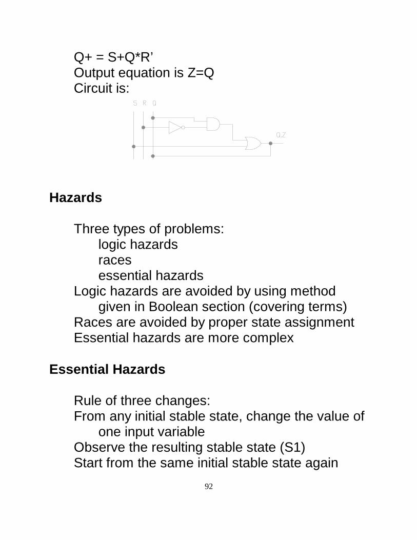
92
Q+ = S+Q*R’Output equation is Z=QCircuit is:
Hazards
Three types of problems:logic hazardsracesessential hazards
Logic hazards are avoided by using methodgiven in Boolean section (covering terms)
Races are avoided by proper state assignmentEssential hazards are more complex
Essential Hazards
Rule of three changes:From any initial stable state, change the value of
one input variableObserve the resulting stable state (S1)Start from the same initial stable state again

93
Make three changes rather than one to the sameinput variable
I.e., instead of 0-1, use 0-1-0-1Observe the resulting stable state (S3)If S1 is different from S3 a possible essential
hazard existsThis is a timing inconsistency that can send the
system to the wrong final stateSolution is to add appropriate delay to feedback
signalsAnalyzing the circuit to find out which delay is
tediousAll possible input changes at all stable states
must be examined!Simulation with accurate timing delays is an
important tool here Toggle Flip Flop
Design as an asynchronous circuitTwo inputs: toggle and clockEdge triggered flip flopAssume output changes take place on rising
edge of clockPrimitive flow table:

94
Toggle Flip FlopTC Output
State 00 01 11 10 00 01 11 10----------------------------------------------------a a b - c 0 - - -b a b g - - 0 - -c a - d c - - - 0d - j d e - - 1 0e k - f e - - - 1f - b f c - - 0 -g - h g c - - 0 -h a h i - - 0 - -i - j i e - - 1 -j k j f - - 1 - -k k j - e 1 - - -
Flow Table Reduction
Note that ouputs made function of inputs also(Mealy form)
This makes reduction easier (opposite ofsynchronous!)
Rows can be matched more easily because ofdon’t cares
First, look for matching rowsStable state in same column, same output,
compatible unstable statesRows d and i can be combinedNext, check for compatible rows for mergingImplication table or merger diagram can be used

95
Combinable rows:a,b; a,c; a,f; c,h; d,k; e,j; e,k
Reduced Flow Table
Not all of these mergers can be madeNot fixed rules for how to do the mergersTry to pick the set that leads to minimum number
of rowsTo avoid confusion, rename the states -- A,B, ...

96
TC Output00 01 11 10 00 01 10 11
-----------------------------------------------------A (a,b) A A F B 0 0 - -B (c,h) A B C B - 0 - 0C (d,k) C D C D 1 - 1 -D (e,j) C D E D - 1 - 1E (f) - A E B - - 0 -F (g) - B F B - - 0 -
State Assignment
If two (or more) variables change"simultaneously"
That is, faster than it takes for circuit to reach anew stable state
The order of change will be interpreted arbitrarilyIf those two variables are state variables, each
interpretation will result in a path through theflow table
(Input variables are "not allowed" to changesimultaneously)
This is a "race"Race can be critical or noncriticalCritical race ends up at different final stable
statesNon-critical races ends up at same stable pointState assignment is done to prevent racesNote - this was not a problem in synchronous
circuits because the clock prevented
97
changes from becoming effectiveimmediately
State Adjacency
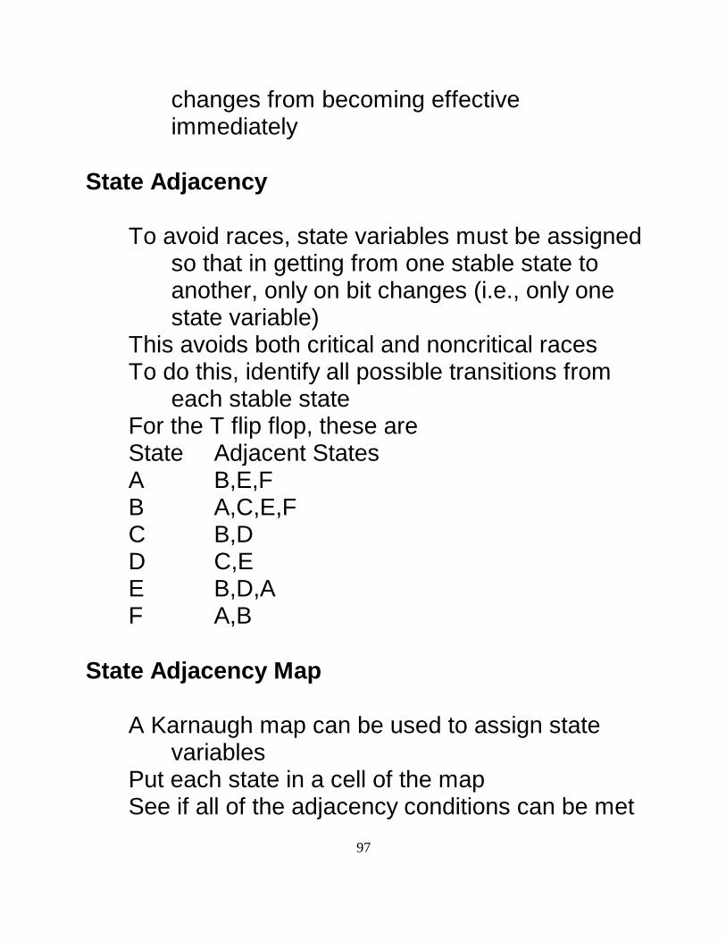
To avoid races, state variables must be assignedso that in getting from one stable state toanother, only on bit changes (i.e., only onestate variable)
This avoids both critical and noncritical racesTo do this, identify all possible transitions from
each stable stateFor the T flip flop, these areState Adjacent StatesA B,E,FB A,C,E,FC B,DD C,EE B,D,AF A,B
State Adjacency Map
A Karnaugh map can be used to assign statevariables
Put each state in a cell of the mapSee if all of the adjacency conditions can be met

98
This is a trial configuration:
It doesn’t meet all of the adjacency requirements(open boxes are don’t-cares)
Bridge States
Next step -- use the don’t-care boxes (if any) toput in extra states
These would be unstable states forming a bridgefrom one stable state to another
Each transition would change only one statevariable
In this case, an assignment with two extra stateswill work:

99
TC Output00 01 11 10 00 01 10 11
-----------------------------------------------------A (a,b) A A F B 0 0 - -B (c,h) A B G B - 0 - 0C (d,k) C D C D 1 - 1 -D (e,j) C D E D - 1 - 1E (f) - A E G - - 0 -F (g) - B F H - - 0 -G - - C B - - - -H - - - B - - - -
Modified Flow Table
The new states, G and H, can bee added to thestate table
The critical transitions are routed through thosestates
This gives the state assignment: (Q1 Q2 Q3)
A:000,F:010,H:110,B:100,E:001,D:011,C:111,G:101This generates a flow table with actual state

100
TC Output00 01 11 10 00 01 10 11
-----------------------------------------------------000 000 000 010 100 0 0 - -100 000 100 101 100 - 0 - 0111 111 011 111 011 1 - 1 -011 111 011 001 011 - 1 - 1001 - 000 001 101 - - 0 -010 - 100 010 110 - - 0 -101 - - 111 100 - - - -110 - - - 100 - - - -
values:
Adding State Variable
The above procedure might not have workedNext step is to add additional state variablesIn this case, minimum number of state variables
is 3Use 4 instead (assuming we couldn’t find the
above solution!)
101
TC Output00 01 11 10 00 01 10 11
-----------------------------------------------------000 000 000 010 100 0 0 0 0100 000 100 101 100 0 0 - 0111 111 011 111 011 1 1 1 1011 111 011 001 011 1 1 - 1001 - 000 001 101 - 0 0 0010 - 100 010 110 - 0 0 0101 - - 111 100 - - - 0110 - - - 100 - - - -
With enough state variables it is always possibleto assign race-free states
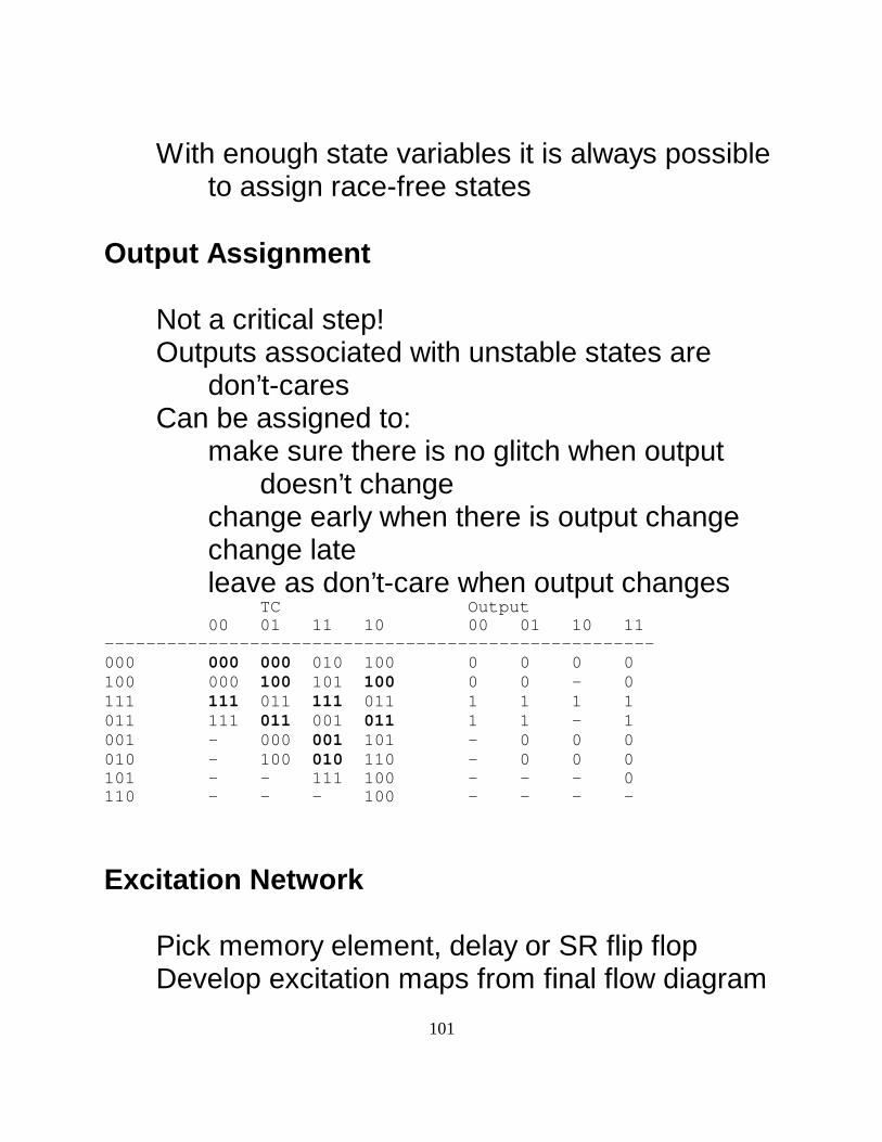
Output Assignment
Not a critical step!Outputs associated with unstable states are
don’t-caresCan be assigned to:
make sure there is no glitch when outputdoesn’t change
change early when there is output changechange lateleave as don’t-care when output changes
Excitation Network
Pick memory element, delay or SR flip flopDevelop excitation maps from final flow diagram

102
State Next State Outputsx1,x2 x1,x2
-----------------------------------------------------00 01 11 10 00 01 11 10
a a b - e 0 - - -b a b c - - 0 - -c - b c d - - 0 -d a - c d - - - 0e f - c e - - - 0f f g - d 0 - - -g h g c - - 0 - -h h b - d 1 - - -
Develop output map from flow diagramApply three-change ruleIf a problem, examine timing
Asynchronous Lock
Solve sequential combination lock withasynchronous circuit
Combination: press and release x1, then pressand release x2
Primitive flow table:
Note that some different decisions were madeabout what happens when user entersincorrect sequence
In the synchronous design, stayed in same stateAsynchronous design returns to starting stateHarder to "pick"
103
Could have been implemented that way insynchronous design also
Exercises: complete the designredo the synchronous design with this logic
for incorrect entries PLDs and Asynchronous Logic
PLDs provide for combinatorial output andfeedback (i.e., no clock)
Some also provide unclocked SR or JK flip flopsIntel software, however, does not provide for
hazard-free minimized excitation equations (Idon’t know about others)
Simplest solution - get the minimized equationsCheck for hazardsAdd additional terms, then disable minimizationOther problem - no way to control delaysPerhaps can be done using extra macro cellIf not, make feedback external to the PLD; add
delay as necessary Metastability
(This discussion based on Intel Application NoteAP-336, "Metastability Characteristics of

104
Intel EPLDs," Thom Bowns)Bistable devices have two stable equilibriaThere is also at least one unstable equilibriumTiming characteristics of sequential circuits are
based on two times: setup time (Tsu) andoutput delay time (Tco)
In synchronous systems, the clock period ischosen to be longer than the sum of theseplus a safety margin
Metastability can occur when Tsu is violatedThis means that an input changes less than Tsu
before a clock edgeWhen that happens, the device could come
close to its unstable equilibriumIt can stay there for a relatively long timeThis violates Tco, which means the circuit is no
longer synchronousResult is unpredictableIn asynchronous circuits, two the rule is that
inputs must change one-at-a-timeMetastable behavior can cause this rule to be
violated Probability of Metastability
Metastable behavior for devices is measured inlaboratory
105
No analytic way to do it!Random inputs are used to drive the deviceOutput timing is measuredLate transitions are categorized as to how lateCan be used to compute parameters describing
unit’s susceptibilityThis can be used to compute a safety marginCan be expressed as mean time between
failures (MTBF)MTBF is a function of clock speedLower clock speed->longer MTBFExample 85C220-80 (nominal maximum clock is
80MHz)For MTBF = 1000 years, Clock = 49 MHz
Failure Probability
Example: 10 systems, each with 5 synchronizerswith MTBF=1000 years
Probability of 1 failure in 5 years is 22%Note - this information is not in the 85C220 data
sheetMetastability is not a problem in the interior of
synchronous circuitsAsynchronous circuits are less predictable
Register Transfer Logic

106
Registers are the basis for general processordesign
Useful for complex problemsIsolates sections of the problemAllows changes to be made ot one section
without affectign othersA register can be thought of as a set of D flip
flopsAll with three-state outputN-bit width, one bit for each D FFN data signals, 2 control signalsOne controls reading (L for load or latch)For example, AND with clock to control data
inputSecond control is the three-state output enable
(OE)It is a level; output is connected when it is TRUEAn additional control input can clear the register
Register Made from D-Flip-Flops

107
Data Bus
Registers are interconnected through a busBus is a parallel set of wiresAll registers connect to the same set of wiresOnly one register can have its output enabledIt will control the voltages on all of the bus wires

108
Any number of registers can read the bus Data Transfer
Transfer data from one register to another, A toB
1st clock tick: set output enable on A to 12nd clock tick: set input enable (D clock) to 1;
data is latched3rd clock tick: set output enable on A to 0, input
enable on B to 0Allowable clock tick rates -- 10-50MHzTime for this operation -- a 60-300 nsWith proper timing of control changes vs clock
edges, this can be accomplished in a singleclock tick
Turn A-OE and B-L on at same timeTiming must be such that output is stable before
data is latched Processors
Can be attached to registersOperate on one or more register outputsResults can be latched to other registersExample: AdderAdds contents of dedicted register to value

109
obtained from busResult is latchedCan be stored anywhere on busCommon procedure - store result back to
originating registerGeneral structure (clock is implied):
Control Signals
Note that the controls are not attached toanything!
All control signals are individually connected to acontrol unit
Control unit generates sequence of controlsignals

110
This sequence produces desired actionThis structure can be generalized to computer
CPUmemorygeneral registersinstruction counter (program counter)memory address registerinstruction registerstack pointerarithmetic unitinput/output bus
Instructions
Computer instructions involve a sequence ofcontrol signals
Instruction taken from memory to instructionregister
Decode instruction to select proper sequenceExecute that sequence of control signalsEach register and processing unit has one or
more control signalsEach of these signals is wired directlySet of all signals is a control wordMany bits!
Microprogram

111
Control unit can be a state machineControl word sequences are implied by the state
machine designAlternate design --Place control word sequences in ROM or RAMControl unit is still state machine, butAbstraction is one level lowerIt picks correct sequence out of microcode ROM
or RAMMicrocode can be changedAllows for processor customizationDifficult to design a microcoded instruction setSpecial purpose -- few software
design/implementation toolsMost complex CPUs are built this wayRISC CPUs might use state machine for ultimate
speed Input/Output Bus
Referred to aboveIs not the bus connected to registers/processorsThat bus is internal to processorData only -- control lines are uniqueI/O bus is for external connectionsAll information is on the busNo separate control signals
112
Bus has:dataaddresscontrol
Devices can be added or removed easily"Non-stop" computers can even have boards
changed while running I/O Bus Interchange
Put address on busThis alerts target systemPut control signal indicating intended operation
(read/write)Put data on bus to complete interactionBus protocol can be synchronous or
asynchronousSynchronous -- clock is a control line on busAll operations must complete within clock cycleAsynchronous -- no clock, uses handshake on
control linesExtra signals, more flexibility
Special Purpose Systems
Design thus far is synchronousControl signals flow from control unit to
113
registers/processorsNo signals coming backControl unit must know number of clock ticks for
each operationAsynchronous design, with handshake, could be
madeExtra signals from processors to control unitWould allow for variable time operations
Example: Optical System
Control unit for optical system connects to busWould require handshake with central control
unitInteraction with optical system is relatively slowData collected could go to memory, or could be
processed directly, e.g., looking for edgesBus design isolates optical system Allows a number of different processing options
to be built around the same optical interface Multiple Buses
It is often useful to move several pieces of dataat the same time
Example: separate bus for instructions and data;multiple data buses

114
Architectures with several buses can producesubstantially faster performance with noclock speed increase
Clock speed increases are expensive -- allassociated components must be upgradedto run with the faster clock
Digital signal processors often use multiplebuses
Specialized for use in digital filtering operationsin real time
Stepping Motors
Motor that can be moved predictably to anyposition without position feedbackmeasurement
Very attractive for applications with predictableload
Target positions are discreteEach position represents a "step"Speed is steps/secWithin specified range, speed can be changed
arbitrarilyDisadvantages: heat, vibration, slower than
servo (dc) systems Permanent Magnet Stepping Motors

115
Synchronous motorEquilibrium position depends on phase of
excitationRotor and stator each have magnetic fieldsMisalignment causes torqueBrings rotor into alignment with statorIf excitation held constant, rotor won’t moveIf torque applied to rotor, it will moveAs it moves, field misaligns applying restoring
torqueActs as a (nonlinear) springHolding torque is maximum torque that can be
applied without exceeding peak restoringtorque
Stepping Sequence
Idealized motor -- three toothed rotorRotor is permanent magnetSouth at center, North at teethStator has windingsWindings operated in opposing pairsa - initial equilibriumb - horizontal stator winding fields reversed, no
motion yetc - motion starts towards new equilibriumd - at new equilibrium
116
Simple Stepping Motor
Excitation Sequence
Bifilar motors -- two windings for each polePoles divided into two sets Horizontal and vertical in simple motorMore poles/teeth in real motorsEach set is wired togetherThis gives 4 inputs - two sets of poles X two
windingsA, B, C, DA, B for one set of polesC, D for the other

117
A B C D----------------1 0 1 00 1 1 00 1 0 11 0 0 1
AB right/left CD top/bottom--------------- ---------------10 NS 10 NS01 SN 01 SN
Exciting A excites one of the bifilar windings, Bthe other
A, B not excited simultaneously; likewise C, D Full Step Sequence
Forward progression gives one direction ofmotion; reverse the other
Sequence wraps around top and bottom Pulse Excitation
Logic circuit to make driving motor easierPulse causes stepDirection of step controlled by logic level signal

118
Pulse signal must be shorter than clockOtherwise additional logic must detect edgeAlternate arrangement -- pulse signal is the clockIt then disappears from the transition conditionsOutput is two variables because that’s all the
information there isOutputs are xyA=x; B=x’; C=y; D=y’
Variable Reluctance Stepping Motors
No permanent magnet

119
Simpler, cheaperRotor is ferromagnetic materialStepping logic is obtained by using different
number of stator poles and rotor teethGives double the step size for same number of
teethPerformance is, in general, not as good
Simple Variable Reluctance Motor
When excitation is changed from 1 to 2, nextposition becomes new stable equilibrium
Stepping Motor Performance
Mass-spring-damper system
120
Magnetic field is nonlinear springVery little damping ...
Resonance
Excitation at near natural frequency will causeresonance
Major enemy of stepping motorCan excite structural resonances in surrounding
mechanical componentsWhen motor itself is at resonance, will no tstep
properlyDefences:
avoid step rates near resonance (switchbetween full/half stepping)
add mechanical damping Static Operation

121
Holding torqueMotor will "slip" if maximum rating is exceededPermenant magnet motor will slip by four stepsWith no feedback of position, system integrity is
lostPermanent magnet motors exhibit detent torqueSmall holding torque present even with power offCan be good, bad or indifferent depending on
application Dynamic Behavior
At slow speeds, static behavior is good modelTransient dies out before next stepAt higher speeds, resonance can be a problemMotor can swing out of range when next step
comesCauses misstepFor slow speeds, step rate can be varied
arbitrarilyAt high speeds, only a narrow range of step
rates is allowedInertia is such that motor will go too far if no step
takes placeHigh speed mode is applicable when load is
largely inertialResistive loads operate strictly in start-stop
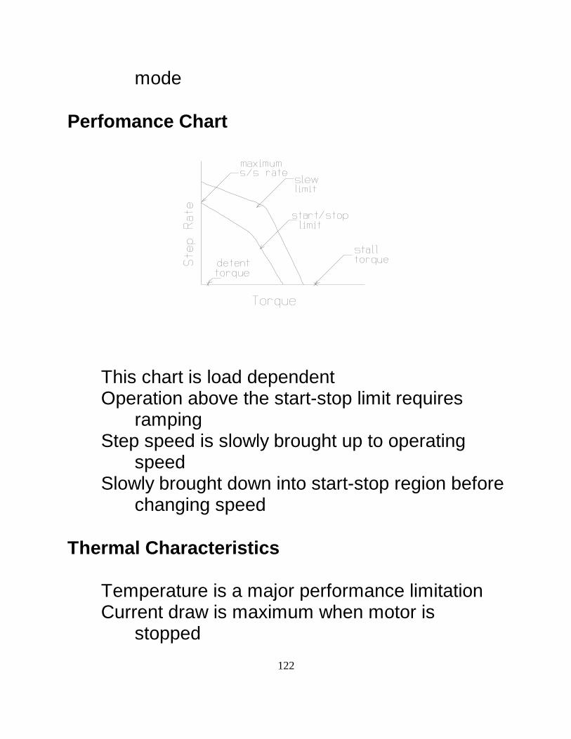
122
mode Perfomance Chart
This chart is load dependentOperation above the start-stop limit requires
rampingStep speed is slowly brought up to operating
speedSlowly brought down into start-stop region before
changing speed Thermal Characteristics
Temperature is a major performance limitationCurrent draw is maximum when motor is
stopped

123
Positioning applications tend to spend most timestopped
Since rotor isn’t moving, cooling is also worstManufacturer voltage limits are based primarily
on steady-state temperatureAdditional cooling allows some increase in
performanceCurrent drives rather than voltage drives can
also improve performanceAt steady-state, rated current is applied to give
rated holding torqueOn transient, voltage will increase substantially
to overcome inductanceLarge voltage is only for short time, so
temperature is not affected substantially Half Stepping
If complete coil set is turned off rather thanreversed, rotor will move one-half of a step
This excitation sequence then gives twice asmany steps per revolution as the full-stepsequence

124
A B C D----------------1 0 1 00 0 1 00 1 1 00 1 0 00 1 0 10 0 0 11 0 0 11 0 0 0
AB right/left CD top/bottom--------------- ---------------10 NS 10 NS00 OFF 00 OFF01 SN 01 SN
Half Step Operation
125
Holding torque at half-step postion is less than atfull step position (about 3/4)
Micro-Stepping
If half step is possible, why not smaller steps?Full, half step sequence can be viewed as crude
approximation to sine/cosine quadratureApplication of true sine/cosine gives arbitrarily
small step sizeMicro step depends only on discretization size
for sine waveDisadvantages
holding torque varies (same range as halfstep)
requires proportional amplifierSwitching amplifier much more efficient, coolerPWM can be used for proportioning; still uses
switching amplifier DC Motors
DC brush motor -- first electric motorFaraday, mid-19th centurySimple -- more voltage -> turns fasterAC power in early 20th century

126
AC motors cheaper to buildDisplaced many DC motor appliationsDC easier to controlRetained difficult control applicationsCan be torque controlled
Coil/Field Interaction
Current-carrying conductor in magnetic field
Not yet a motor -- coil will seek equilibriumposition
Commutation
Current flow in coil must be made function ofposition
Reverse direction every time torque startsdecreasing

127
This can be done with brushesThese amount to a mechanical switching control
system
Coils on rotorStator is permanent magnetStandard configuration for brushed "servo" or
"torque" motors Multi-Coil Motor
Avoid top-dead-center problemsMake generation of torque more uniform

P'Vi'JS
128
Operating Characteristics
Control volume view of motor"Motor" box is lossless, stores no energy
Power flow on mechanical, electrical sides mustmatch instantaneously
Motor Equations
Mechancial power = electrical power

J'KJi
P'Vi'JS'KJiS
V'KJS
V'KES
dSdt
'
J
J
129
From electromagnetic theory,
If the field applied by the stator is constant,
so,
This is the back-EMFUsually written as a separate quantity
But, torque constant and back-EMF constant arereally the same if written in same units
Motor-Driven System
Voltage amplifierInertial load
Mechanical side, Newton’s law,
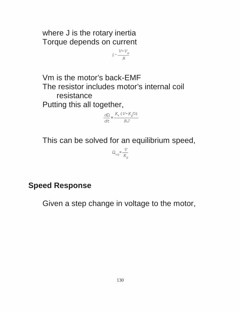
i'V&VmR
dSdt
'
KJ(V&KES)
RJ
Seq'VKE
130
where J is the rotary inertiaTorque depends on current
Vm is the motor’s back-EMFThe resistor includes motor’s internal coil
resistancePutting this all together,
This can be solved for an equilibrium speed,
Speed Response
Given a step change in voltage to the motor,

131
Curve shows response for two different inertiavalues
Note that rise time is affected but not equilibriumspeed
Generators/Tachometers
The operating equations do not depend ondirection of power flow
Mechanical power in -> electrical power outThis is a generatorIt also describes dynamic brakingWhen operated for its output power, it is called a
generatorCan also be operated as a speed sensorMeasure open-circuit voltageBack-EMF proportional to speed

132
This is a tachometer Brush Problems
Despite simplicity, brushes have problemsELectrical noiseWear outCan only apply on/off controlLimit maximum voltagesBrushless motors
DC Motor Types
Field woundUses coil on stator to provide fieldSelf-excited -- use same voltage source for rotor,
statorSeries, shunt, compound windingSeries: high starting torque, drops off rapidlyShunt (parallel): flatter torque curve before drop-
offCompound (mixture of series an parallel): in
betweenReversing self-excited motors is tricky
Permanent Magnet Motors

133
Use permament magnet on stator to producefield
Main choice for high torque, precision controlapplications
No current needed for static fieldRuns coolerVery effective modern magnet materialsMagnets can be permanently demagnetized by
too much current! Iron/Ironless Core Motors
Maximum torque - iron core rotorhigh magnetic permeabilty, strong magnetic
fluxRotor has high inertia because of all of the ironBut is capable of delivering high torque
Maximum acceleration - ironless core motorIf load has very low inertiaAcceleration is very importantUsually built in either pancake (flat) or shell
configurationLess torque capability, but very fast acceleration,
smooth operation Linear Motors
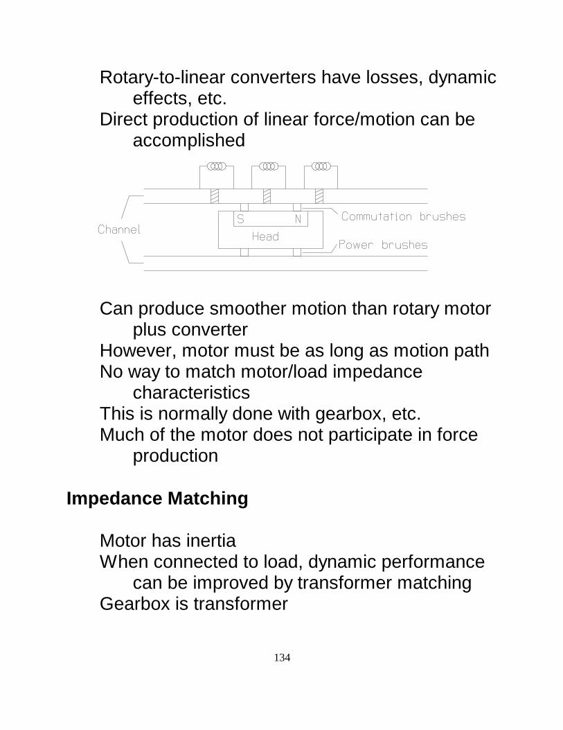
134
Rotary-to-linear converters have losses, dynamiceffects, etc.
Direct production of linear force/motion can beaccomplished
Can produce smoother motion than rotary motorplus converter
However, motor must be as long as motion pathNo way to match motor/load impedance
characteristicsThis is normally done with gearbox, etc.Much of the motor does not participate in force
production Impedance Matching
Motor has inertiaWhen connected to load, dynamic performance
can be improved by transformer matchingGearbox is transformer
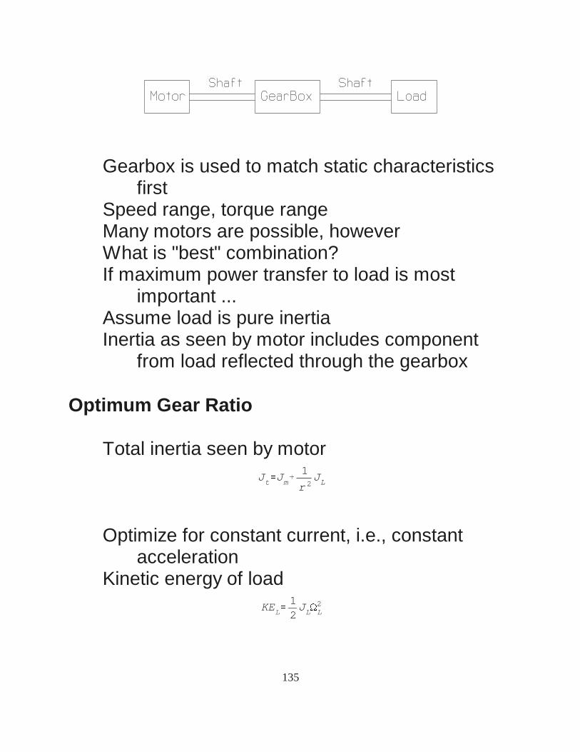
Jt'Jm%1
r 2JL
KEL'12JLS
2L
135
Gearbox is used to match static characteristicsfirst
Speed range, torque rangeMany motors are possible, howeverWhat is "best" combination?If maximum power transfer to load is most
important ...Assume load is pure inertiaInertia as seen by motor includes component
from load reflected through the gearbox Optimum Gear Ratio
Total inertia seen by motor
Optimize for constant current, i.e., constantacceleration
Kinetic energy of load

P'ddt
KE'JLSLdSLdt
PL'JLr 2
Sm
dSmdt
dSmdt
'"m'Jm
JT; Sm'"mt
PL'JLJm
2t
r 2JT2
M(r(Jm%1
r 2JL))
2
Mr'0
Jm&1
r 2JL'0; Jm'
1
r 2JL
136
Differentiate wrt time to get power
Reflect this back to the motor
Acceleration is proportional to applied torquedivided by total inertia
Since acceleration is constant; Power to load is
Optimize by finding MAX of this wrt gearboxratio, r
Only denominator depends on r, differentiate wrtr and set to zero
This is zero at

137
But, this is just the load inertia reflected at themotor
In other words, adjust r so impedances match Thermal Characteristics
Heat is a primary performance limitationSources:
electrical losses in windingeddy currentshysterisiswindagefrictionshort circuit currentsbrush contact resistance
Detailed analysis separates rotor and housingTransient limits very different from steady-state
limits Motor Control
Voltage controlPower amplifier produces an output voltage in
response to input commandMotor speed is load dependentZero command produces braking (due to
electrical dissipation)

138
Current/torque controlCan’t be done directly, normally uses feedback
around amplifierFeedback compensates for back-EMFImproves dynamic performance -- voltage rises
sharply during initial transient
Velocity Control
Uses a velocity measurementTachometer, resolver, encoder
Either voltage or current amplifierProportional controlUsing voltage amplifier

139
Using current amplifier
Gain Limitations
For simple model, no gain limits!

140
Practical applications have some additionaldynamics
It will limit gains, even if primary dynamics don’tProportional control for system including
armature dynamics
Dynamic Compensation
Control theory provides means for compensatingknown dynamics
Lead-lag compensator can be added to abovesystem
For highest gain case, this gives
141
Position Control
Cascade control uses velocity and positionmeasurements
Position control can be done with just a positionmeasurement

142
Position Control Results
Using cascade control, proportional control only
Using position measurement only, proportionalcontrol

143
Above uses current amplifierIf current amplifier is replaced with voltage
amplifierResponse is more stable -- voltage amplifier
provides dampingBut it is also slower

144
Alternate would be to use more complex controlstructure
Velocity would, in effect, be estimated
Brushless Motors
Motor with no electrical contact to rotorSame general performance specification as DC
brush motorDC-brush, AC induction, stepping motor:

145
Brushless Motor Configuration
Permanent magnet on rotorThree phase excitationRequires rotor angular position measurement

146
DC Excitation
Uses three-phase DC signalsRequires three channels of power amplificationExcitation is a function of rotor positionOn-off excitation just needs discrete point
measurementHall effect sensors are common
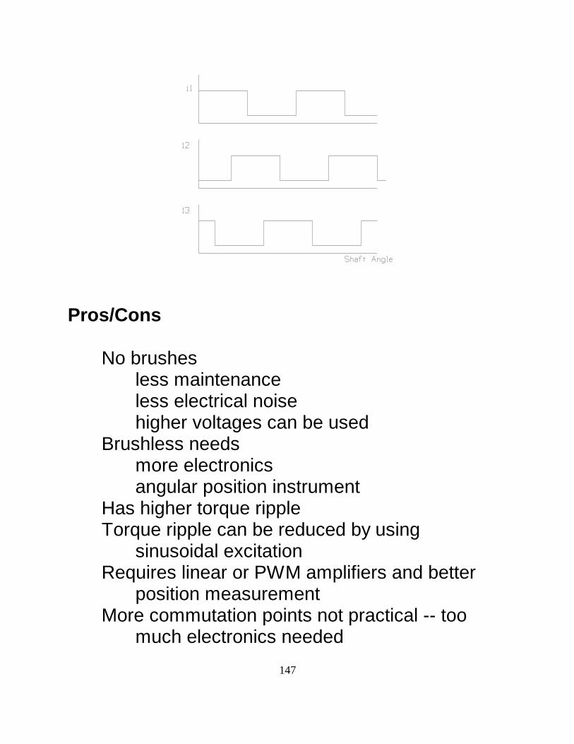
147
Pros/Cons
No brushesless maintenanceless electrical noisehigher voltages can be used
Brushless needs more electronicsangular position instrument
Has higher torque rippleTorque ripple can be reduced by using
sinusoidal excitationRequires linear or PWM amplifiers and better
position measurementMore commutation points not practical -- too
much electronics needed

148
Analog <--> Digital Conversion
The physical world is analog (to commonengineering view)
All information must be convertedConversion can be part of instrument actuator
stepper motorincremental encoder
Or analog electrical signal can be convertedexplicitly
Analog/digital conversion interfacesA/D puts analog electrical signal in form usable
by computerD/A puts computer word in analog form
Coding
Digital world is finite precisionCoding is arbitraryOnce in a computer, codes are relatively easy to
convert from one form to anotherNormal coding
analog information <--> digital integerAnalog information is usually voltage or currentThere are several forms for digital integers
Integer Codes

149
Voltage Digital DecimalValue Equivalent
_______________________________0 000 00.71 001 11.43 010 22.14 011 32.86 100 43.57 101 54.29 110 65 111 7
Unipolar voltages can code to unsigned integersThree-bit example (3 bits will be used for next
few examples)Assume voltage range is 0-5 volts
Bipolar Voltages
Assume -5 to +5 volt rangeTwo common codings
offset binarytwos complement

150
Voltage Digital DecimalValue Equivalent
_______________________________-5 000 0-3.57 001 1-2.14 010 2-0.71 011 3+0.71 100 4+2.14 101 5+3.57 110 6+5 111 7
Voltage Digital DecimalValue Equivalent
_______________________________--- 100 -4-5 101 -3-3.33 110 -2-1.67 111 -10 000 0+1.67 001 1+3.33 010 2+5 011 3
Note that there is no code for 0 voltsThis comes from basic asymmetry -- even
number of codesThis code is simple to implementPopular with converter manufacturers
Twos Complement Coding
Most common coding used in computers forsigned integers

151
Main problem with 2’s complement coding ismatching word size
A/D, D/A converters rarely match computer’sword size
To convert, fill to the left is sign dependentNegative numbers must be filled with 1s, positive
with 0sExample, the 3 bit, 2s complement number 101
is 111101 when converted to 6 bit widthThe 3 bit, 2s complement number 011 is 000011
when converted to 6 bit Digital-to-Analog Conversion
Digital value is stored in a register, thenconverted
Output remains the same until next value is sentto register
Control terminology -- this is a zero-order holdConversion time is very fast -- just rise time of
output amplifier

152
3-Bit Converter
Uses analog switches, constant multipliers,summation
Good conceptual modelNot practical for more than 2 or 3 bitsWide range of circuit componentsNoise, parameter drift problems

153
Voltage DigitalRange Value_________________0-1.25 001.25-2.5 012.5-3.75 103.75-5 11
Flash Analog-to-Digital Conversion
A/D much more complicated than D/A!Flash converter uses comparators to determine
input voltage rangeLogic converts comparator outputs to digital
valueOperates very fast -- 10-100 ns convert timeTypically 4 to 8 bit precision
2-Bit Flash Converter
Code:
3 comparators:C1: V>1.25C2: V>2.5C3: V>3.75
To get output value, use the truth table,

154
C3 C2 C1 H L___________________000 00001 01010 --011 10100 --101 --110 --111 11
Practical Issues
Converter uses natural binary countingIf input is changing, out-of-range values will be
producedSample/hold must be used on input to prevent
thisOutput is only valid a specified time after input is
heldContinuous sampling can be done with Gray
codeAs input changes, outputs are guaranteed to be
continuousLots of comparators - 255 of them for 8-bit
converterAdjacent comparatora must have monotonic
range change
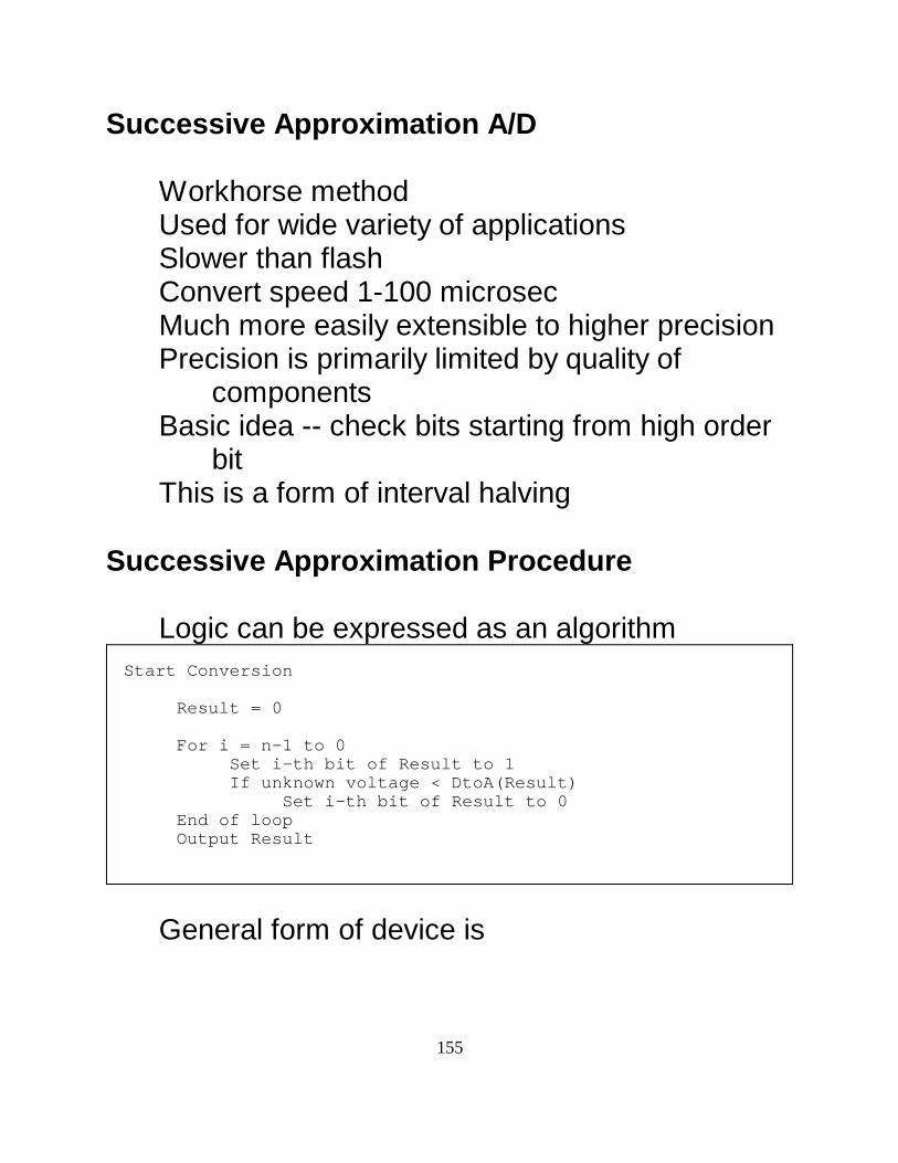
155
Start Conversion
Result = 0
For i = n-1 to 0Set i-th bit of Result to 1If unknown voltage < DtoA(Result)
Set i-th bit of Result to 0End of loopOutput Result
Successive Approximation A/D
Workhorse methodUsed for wide variety of applicationsSlower than flashConvert speed 1-100 microsecMuch more easily extensible to higher precisionPrecision is primarily limited by quality of
componentsBasic idea -- check bits starting from high order
bitThis is a form of interval halving
Successive Approximation Procedure
Logic can be expressed as an algorithm
General form of device is

156
Configuration
Convertor is quite expensiveUsually used with a multiplexorMany channels feed a single converterEffective conversion speed depends on number
of channels usedSample/hold normally precedes converter
Direct Memory Access (DMA)
When fast conversion of a succession of valuesis needed
No action until all values are inDMA gives converter direct access to memoryCPU is simply suspended for a few cyclesMuch faster than interrupt or program controlDMA controller acts as master processor during
transfer cycle

157
Also used for disk drives, other high speedperipheral devices
Integrating Converters
Slowest of the commonly used converters (manymillisec)
Can be made very accurate and preciseUsed in DVMs, for example (several
conversions/sec)Uses timing to determine digital value of
unknown voltageSimplest form --
Multiple Slope Integrating Converters
Dual slope
158
Integrate unknown voltage up for fixed timeFind time necessary to integrate back to zeroValue is related to ratio of timesCancels effects of several circuit componentsHigher-order integration schemes can remove
even more Sigma-Delta (1-bit) Converters
Symmetric structure for A/D and D/ASpeed range similar to successive approx.
convertersOperating principle is closest to PWMModulated signal is createdBinary modulation (ratio of 1s to 0s)Commonly used in CD players Sigma-Delta Modulation
Feedback structure produces 1-bit modulated signalComparison to input is used to force average value
to match input --

Integrator Comparator
Scaler
V in Filter+
-
1-bit
1-bit
V-scale
V-scale V-scale
F-scale
159
Figure 71. Sigma-Delta Converter Structure
V-scale is input units/modeF-scale is output units/mode1-bit is digital 1-bit signal Operation
Scaler produces extremum values in V-scale domainComparator switches as its input crosses mid-range
of V-scale (usually 0)If loop remains stable, output of comparator will have
average value of inputFilter is used to turn modulated digital signal into
useful value in F-scale domain Sigma-Delta A/D Converter
Use analog on input domain, n-bit digital for output --

Integrator 1-bit ADCV in Filter+
-
1-bit
1-bit
Analog
Analog Analog
N-bit
1-bit DAC
160
Figure 72. Sigma-Delta A/D Converter
The 1-bit ADC and DAC are what makes thisconverter easy to implement in hybrid system
Performance
V-scale: -1.0 to +1.0; F-scale: 0.0-1.0Vin = 0.3

161
Figure 73. Sigma-Delta Converter Operation - Integratorand Comparator
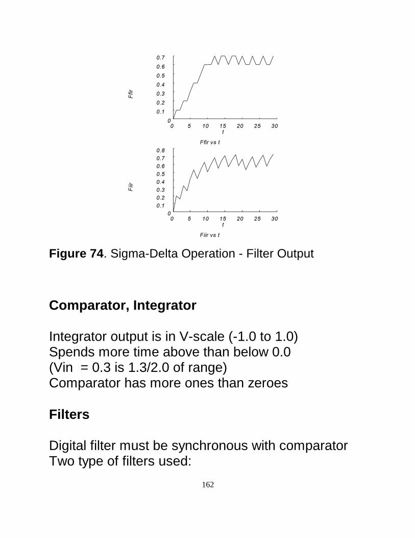
162
Figure 74. Sigma-Delta Operation - Filter Output
Comparator, Integrator
Integrator output is in V-scale (-1.0 to 1.0)Spends more time above than below 0.0(Vin = 0.3 is 1.3/2.0 of range)Comparator has more ones than zeroes Filters
Digital filter must be synchronous with comparatorTwo type of filters used:

yk'(1&C)yk&1%Cuk
yk'C0uk%C1uk&1%C2uk&2%...
163
(22)
(23)
Infinite impluse response (IIR)
Similar to analog filter in outputOutput approaches final value exponentially (infinite
tail)Righthand side has both u and y terms Finite impulse response (FIR)
Finite tail - reaches exact final valueRighthand side has only u termsWith Cs all = 1.0, boxcar (comb) filterExample uses boxcar, n=10Response similar to 1st order IIR filterBut, for [1,0] input, no multiplications! Resolution
Output variation about 1 part in 20About 4-bit converterSimilar resolution for IIR and FIRFIR resolution can be tricky, Vin = 0.0 --

Accumulator Comparator
Scaler
V in Filter+
-
1-bit
1-bit
N-bit
N-bit N-bit
Analog
164
Figure 75. Filter Output for V =0in
Figure 76. Sigma-Delta Digital-to-Analog ConverterStructure
Sigma-Delta D/A Converter
Same structure, change domain definitions

165
Filter is analogVery cost effective in high volumesPerformance curves above also apply to D/A Design Considerations
Modulator - these are 1st orderHigher order is possibleFeedforward and feedback structuresFeedback simpler but subject to instability
Filter - big subject!Determines rise time and resolutionIn ADC, IIR or FIR
CostUsed in high volumes, and as part of integrated
circuitsUnit cost is very important Sampling
When data is sampled information is lostSampling theorem (Shannon, Nyquist) gives
limitsSampling rate must be faster than twice highest
frequency present

166
(Even if highest frequency is noise)Slower sampling will lose frequency information,
but retain amplitude informationThis is called aliasingAnti-alias filter is analog filter that precedes
converter
Oversampling
Sample much faster in converter than needed by

167
applicationAnti-aliasing can be split between analog and digital
filteringMore flexibility if computing power is availableDigital signal processor (DSP) is often used for
filteringVery useful in sigma-delta ADC since filter is there
anyway Sub-Sampling/Decimation
Stream of oversampled data has more data valuesthan can be used
Sub-sampling throws away (n-1)/n of the dataFIR filters are particularly useful hereBecause rhs depends only on inputs filter ouput only
has to be calculated when neededThis is called decimationPerformance of filter is unaffectedIIR filters require output to be calculated even if not
used Position and Velocity Measurement
Measurements used in all mechanical systemsAlso used in mechanical components of process
systems

168
e.g., valve motionMany media availableWe will concentrate on electrical outputs
Precision, Range, Accuracy
Range --Position - smallest resolvable increment divided
by maximum movementVelocity - ratio of largest to smallest velocityFor velocity, "stopped" is a special caseFor position, word size is the major limitationDifficult in hardwareComputers can trade arbitrary precision against
computing speedAnalog vs. digitalAnalog lacks dynamic range but more intuitiveComputer processing become dominant, so
digital more attractiveComputational speed major limitation
Analog Velocity Measurement
TachometerDC motor/generatorOpen circuit on electrical sideRuns as an unloaded generator

VT'KvS
169
Since current is zero, the other half of the motorequation is irrelevant
Noise:brushes, commutation switching transients
Design based on noise reduction -- heat not anissue
Low velocity performance limited by analognoise level
High velocity limit is voltage limit of attachedequipment
Stopped/Not Moving
Special conceptRequires good low velocity measurementDifferent from very slow!Wait for specified period to define stoppedApply a brakeMechanical systems "stop" because of stictionUnique to mechanical systemsCurse and blessing!Low velocity scanning also needs good
measurement

G(s)'T1s%1
T2s%1
170
Velocity Control
"Tach loop"Analog implementation with operational
amplifiersCommon configuration - provides stabilityDigital systems becoming more commonSimplest variant - read velocity with ADCControl compensation in velocity loop to improve
performanceCompensates for motor inertia and coil
inductance Lead/Lag Compensator
Can be lead or lag, depending on parameterratio
Lead adds differentiator behavior - stabilizesLag adds integrator behavior - reduces steady-
state error
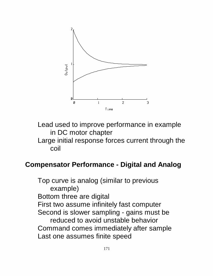
171
Lead used to improve performance in examplein DC motor chapter
Large initial response forces current through thecoil
Compensator Performance - Digital and Analog
Top curve is analog (similar to previousexample)
Bottom three are digitalFirst two assume infinitely fast computerSecond is slower sampling - gains must be
reduced to avoid unstable behaviorCommand comes immediately after sampleLast one assumes finite speed
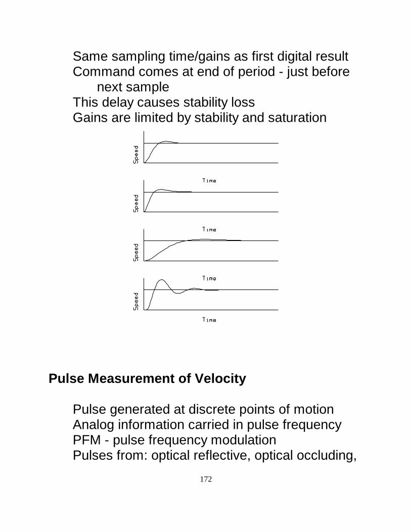
172
Same sampling time/gains as first digital resultCommand comes at end of period - just before
next sampleThis delay causes stability lossGains are limited by stability and saturation
Pulse Measurement of Velocity
Pulse generated at discrete points of motionAnalog information carried in pulse frequencyPFM - pulse frequency modulationPulses from: optical reflective, optical occluding,

173
magnetic, pressure, reluctance, mechanicalswitch
Good for unidirectional problemsFrequency-voltage convertersRequires additional conversion for digital controlNot very common in modern systems
Logic Measurement of Frequency
Timer, counter, control logicCount pulses for fixed period of timeResult is frequency -- proportional to speedSimple logic diagram:

174
Logic Measurement with Error Check
Add check for overflow to avoid erroneousreadings
Further safety device - use handshake to makesure output information is only read whenvalid
Will work in software also - usual speed caveatsCan be implemented as interrupt/asynchronous
functions

175
Precision
Ratio of timing period to pulse periodAccuracy of the timingFirst is function of velocityHigh velocity, lots of pulses->high precisionLow velocity, few pulses->low precisionPrecision can beincreased by increasing the
sampling periodOnly up to a limit based on control/measurement
needsAccuracy depends on clock frequency and
latency Period Measurement
Precision/velocity characteristics complementaryto frequency measurement
Start a timer on rising edge of pulseStop it on next rising edgeSame types of error and precisionClock frequency vs. pulse periodAdditional problem -- uneven spacing of pulse
generating elementOther solutions:
switch between frequency, period
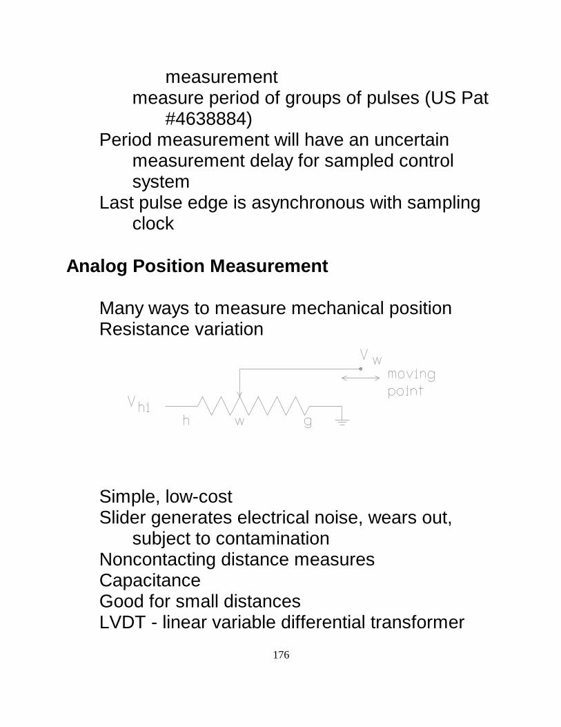
176
measurementmeasure period of groups of pulses (US Pat
#4638884)Period measurement will have an uncertain
measurement delay for sampled controlsystem
Last pulse edge is asynchronous with samplingclock
Analog Position Measurement
Many ways to measure mechanical positionResistance variation
Simple, low-costSlider generates electrical noise, wears out,
subject to contaminationNoncontacting distance measuresCapacitanceGood for small distancesLVDT - linear variable differential transformer

177
AC excitedCore changes relative coupling to secondary
coilsAC output must be converted to DC to be useful
Hall Effect
Hall effect sensors detect magnetic fieldsPermanent magnets + Hall effect sensor =
position sensorMagnetic field changes pattern of current flow in
a thin semiconductor sheetTherefore, voltage across sheet changes, ~100
microvoltsEither magnetic or sensor can move

178
Gives noncontacting sensorRequires magnet, which could could generate
unwanted forces Incremental Encoders
Related to pulse generatorsExtends dynamic range of analog position
instrumentsUses quadrature + index pulseQuadrature is two channel signal, 90 deg. out-of-
phase
Quadrature Decoding
Decoders usually convert quadrature to twopulse channels
One for forward counts, one for backwardThese can be sent to up/down counter
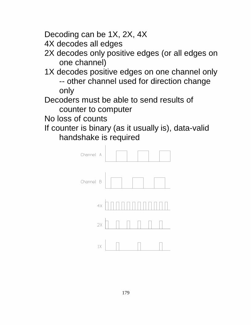
179
Decoding can be 1X, 2X, 4X4X decodes all edges2X decodes only positive edges (or all edges on
one channel)1X decodes positive edges on one channel only
-- other channel used for direction changeonly
Decoders must be able to send results ofcounter to computer
No loss of countsIf counter is binary (as it usually is), data-valid
handshake is required
180
Reliability
Primary disadvantage -- incremental informationonly
Index pulse used for homingNo way to recover from errorsI.e., errors are cumulativeDecoder must not miss any transitionsQuadrature rate often up to 1MHzCan be doneNo limit to dynamic rangeQuadrature is grey code -- if two bits change that
is an errorSingle-ended vs. differential wiringGlass construction can be fragileAlignment is very important
Optical Shutter
Fixed, moving grateLight source on one side, detector on the otherThis allows grid size to be smaller than light
source

181
Two receivers/fixed grids appropriately alignedgive quadrature
For crude grids, only moving grid is neededOther technologies can be used to generate the
signalMagnetic has been used commerially
Micro Decoding
Most application convert signal to digitalAnalog signal from each channel is (ideally)
triangular
Two channels give 90 deg. out-of-phase trianglewaves
Real signals are much more sinusoidalAs long as shape is reproducible, it can be
decoded to get position

182
Limit is then determined by analog noise Velocity from Encoders
Same as pulse frequency measurementLogic is complicated by change in directionSimplest method is to difference the positions at
fixed sample timesPrecision no good at low velocityPeriod measurement can be used, but must take
direction change into account Linear, Rotary Encoders
Encoders can be built for either rotary or linearmotion
Rotary motion can be measured directlywithrotary encoder
Linear motion has several choicesLinear encoderOne grid must be length of encoderIt is fixed to one side of movementOther side is a small carriageIt contains light source, small grids, light
detectorsGives greates accuracy since it directly
measures motion of interest

183
Or, rotary encoder can be attached torack/pinion
Can be less expensive than linear encoderAccuracy depends on quality of rack/pinionRotary encoder can be attached to motor shaftAccuracy depends on accuracy of drive system
(lead screw, etc.) Laser Interferometry
Type of encoderIncremental motion informationExpensive, preciseDown to about 2 nanometer resolutionOutput depends on phase difference between
signal reflected from moving object andreference signal
Laser is necessary to get phase-coherent,mono-frequency light
Major errors are from alignment problems,temperature changes in air path, motion ofair causing density changes

184
Synchros and Resolvers
Analog, AC devicesGive absolute position informationCan also generate a velocity signalCompete with incremental encodersUse rotating and fixed coils

185
AC excitation to rotating coilSignal introduced to rotating coil via brushNo commutation segments, so less noise
problemResolver is 4 wire device, synchro is 3 wire
Resolver Outputs
Vx'(Ksin2)sinTt
Vy'(Kcos2)sinTt
186
Outputs from resolver are amplitude modulatedAC signals
Resolver processing is often described as phasedetection
It isn’t, howeverShaft position information is contained in
amplitude modulation of the output signalsPhase and frequency are nominally the same for
bothSome errors in actual devices --Phase shift due to rotor motionVoltage induced by rotor motion (back EMF)
Conversion to Position and Velocity Signals
Idealized conversion systemDoesn’t correct for any errors

cos(N)sin(2)sin(Tt)
sin(N)cos(2)sin(Tt)
sin(2&N)sin(Tt)
187
Feedback Position Estimation
Start at point marked "estimate of shaft angle"This is a DC analog signal, i.e., no modulationIt is the device’s position output signalOutputs of resolver are as described aboveTherefore, outputs of the multipliers are:
(K set to 1 for convenience)When subtracted, these give,
188
Has error in shaft positionThis can be used as input to a feedback loopFirst, must get rid of ACThis can be done by dividing by referenceWe now have a demodulated signalIt is errorPut it through PI elementThen integrate to close the loopInput to integrator is estimate of velocity

189

190
Resolver-to-Digital Converter
Same basic schemeMajor difference is replace integrator with
counterDrive counter with VCO (voltage controlled
oscillator)Input to VCO is output of PIDemodulator handles most of error correction

191
Overall precision 12-16 bitsAbsolute position output within a single
revolution Rotary, Linear Multistage Configurations
Rotary devices onlyRack/pinion gearing can be usedAbsolute over motion range usually depends on
gearingResolvers have limited dynamic range (unlike
incremental encoders)Can be configured as fine/coarse with gearing
Absolute Encoders
Multi-channel extension of incremental encoderOne track for each bit of resolutionRotary onlyDigital alternative to resolverOptical or brushThree common codings:
natural binarybinary-coded decimalgrey code

192

193
First two codes have multi-bit changesGray binary conversion
b(k-1) = b(k) XOR g(k-1)Start computation with k=n
Operational Amplifiers for Analog SignalProcessing
Effortless parallel computation!Analog computing elementsImplement linear analog functions with high
fidelitySome nonlinear functions can also be
implemnentedNot as faithful reproduction of nonlinear
functionsCircuit functionality can be made to depend only
on passive componentsI.e., resistors, capacitors, diodesIndependent of properties of amplifier (which is

194
the active component)Passive components can be much better
controlled and characterizedAnalog computers were used for generalproblem solvingSystems based on differential equationsNow, op-amps mostly used for signal
conditioning and instrumentationUsed for filtering, isolation, rectification, limitingUsed at midlle level of signalsAfter initial amplification from very low power
levels High-Gain DC Amplifier
Op-amp: very high gain amplifierDifferential inputsSingle-ended output
Normally used with bipolar power supply givingbipolar output range
Internally -- multi-stage transistor amplifier741 has ~20 transistors + resistors and

195
capacitorsPlain op-amp not very usefulHas gain of 10 or higher5
100 microvolts or less will cause full scaleexcursion of output!
The actual value of the gain is not very reliable Op-Amp with Feedback
Feedback can tame the beastAdd passive feedback components to degrade
the gainThis is what makes the device useful!When feedback is added the overall circuit
characteristics depend only on the passivecomponents
Major invention of the 1930sSimilar devices were done earlier, but not
understood as computing circuitsFlapper-nozzle valve is pneumatic op-ampPneumatic systems were too complex to
recognize the computing simplicityDerivation of operating characteristics starts
from ideal op-amp definition:-Infinite open loop gain-Infinite input impedance (draws no current)-Zero output impedance (voltage

if'VoutRf
196
independent of load) Computing Amplifier Equations
"Inverting amplifier" configuration:
Application of ideal characteristics leads toconclusion that voltage V must be nearly-
zeroThis follows from high gainIf it were not very small, output would be
saturated (at limit value)V sometimes called "virtual ground"-
Voltage is always nearly ground, but notconnected to ground
Input and feedback currents can be computedfrom this information

iin'VinRin
if'&iin
Vout'&RfRin
Vin
197
Amplifier draws no current at its inputs, so
Substituting -
Isolated Gain
This circuit provides a gainGain value is determined only by resistor valuesDifference from use of voltage divider (pot):
gain can be greater than one (or less)input impedance can be higherouput impedance is lower
Typical op-amp applicationFeedback resistance provides negative
feedbackReduces overall gainCurrent at virtual ground (also called summing
juncdtion) sums to zeroSign inversion -- annoying characteristic comes
from summing currents
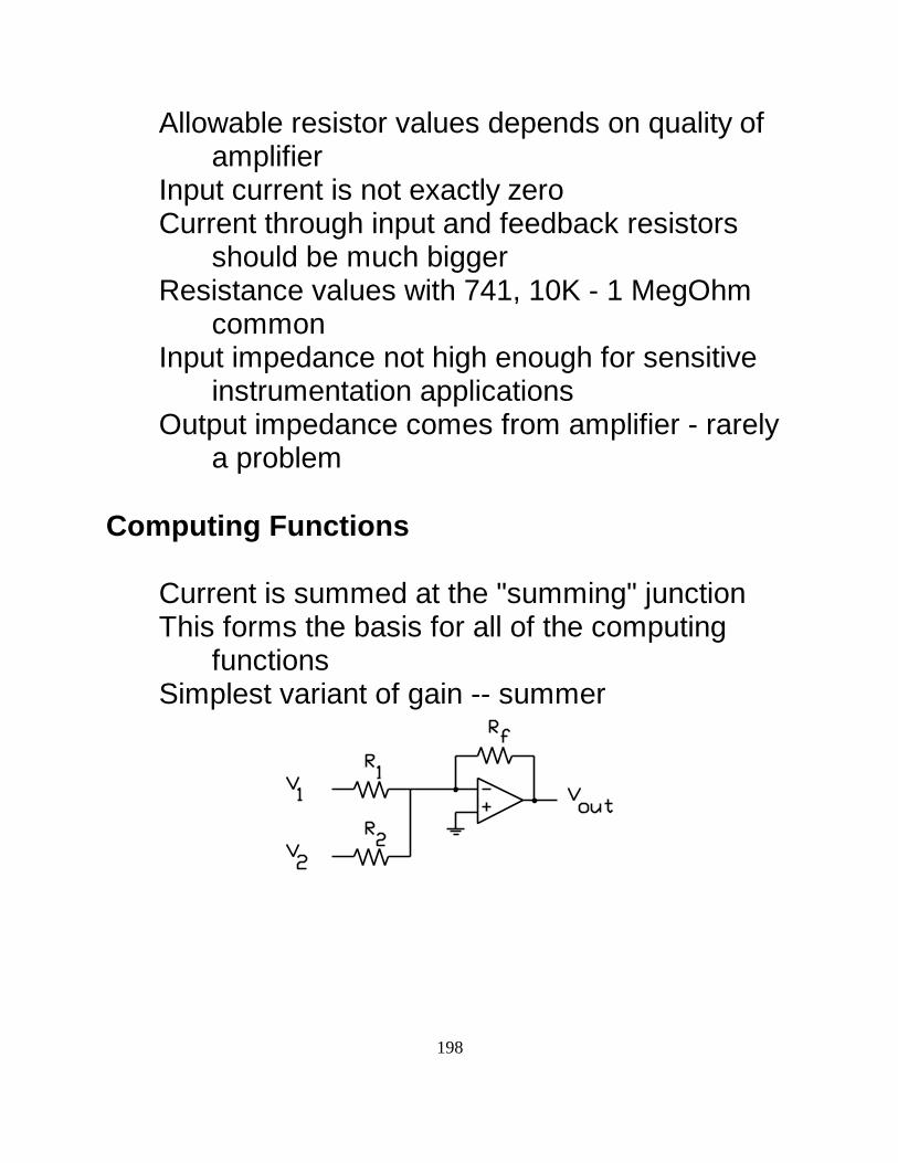
198
Allowable resistor values depends on quality ofamplifier
Input current is not exactly zeroCurrent through input and feedback resistors
should be much biggerResistance values with 741, 10K - 1 MegOhm
commonInput impedance not high enough for sensitive
instrumentation applicationsOutput impedance comes from amplifier - rarely
a problem Computing Functions
Current is summed at the "summing" junctionThis forms the basis for all of the computing
functionsSimplest variant of gain -- summer

if'&(i1%i2)
Vout'&(V1
R1
%
V2
R2
)
Vout'&R1
RfV1&
R2
RfV2
if'CfdVoutdt
Vout'&1
RinCfmVindt
199
Any number of such inputs can be used Integrator
Functional characteristics again depend only onpassive components

Vout'&RfCindVindt
200
This time, capacitor and resistorSumming integrator made by adding inputs
Differentiator
Reverse capacitor and resistor --
This resistor is "too good"It is very noise sensitiveIt can be desensitized by adding a small
capacitance in parallel with the feedbackresistor
This turns it into a low-pass filter for highfrequencies
I.e., it ignores high frequencies Low Pass Filter (First-Order Lag)

dVoutdt
%
1RfCf
Vout'&1
RinCFVin
Vout'
&
1RinCf
(s%1
RfCf)Vin
201
Any number of elements can be combined tomake an input or feedback network,
This circuit satisfies the differential equation -
Which is equivalent to the transfer function -
Could be used as an anti-aliasing filter for anA/D converter
Analog Commputers
We now have everything needed to solveordinary differential equations
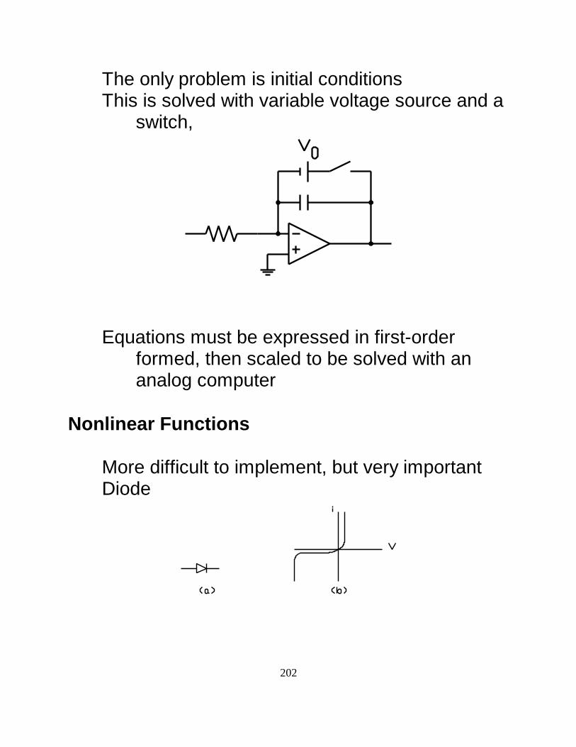
202
The only problem is initial conditionsThis is solved with variable voltage source and a
switch,
Equations must be expressed in first-orderformed, then scaled to be solved with ananalog computer
Nonlinear Functions
More difficult to implement, but very importantDiode

203
Ideal diode conducts current only in one directionReal diode
-offset voltage to enter conducting state-offset is about 0.6 in silicon diodes-Reverse direction has small, but finite
resistance-Has a breakdown voltage for reverse bias
Reverse bias is not encountered in normaldiodes (~75 volts)
Used in zener diodes which have highlypredictable breakdown voltage
Diode Limiter (Clamp)
Simple clamp limits voltage to only positive ornegative
When diode is conducting (V > 0 in this case)out
the amplifier gain becomes zeroReverse direction of diode to block negative
output voltages

204
Add a bias voltage to clamp at an arbitraryvoltage,
Absolute Value
This circuit will produce the absolute value of aninput voltage
Works by adding the negative of the clampedinput to twice the original signal
Has two op-amps so produces non-inverted
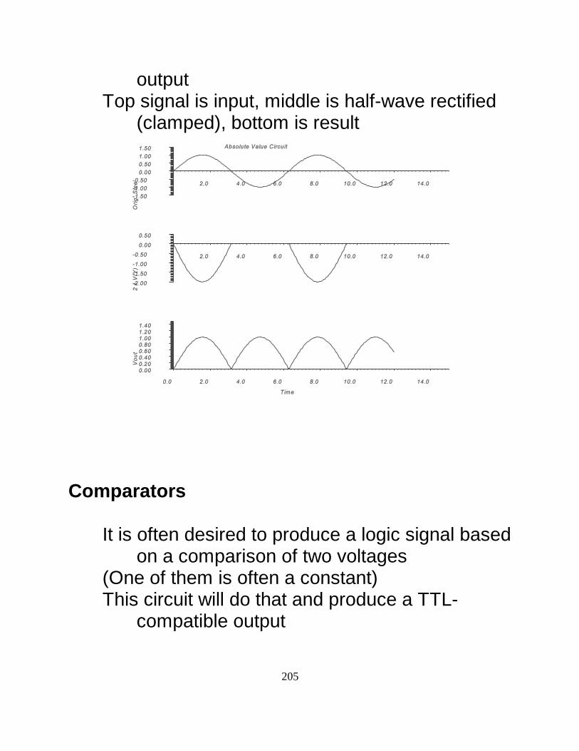
205
outputTop signal is input, middle is half-wave rectified
(clamped), bottom is result
Comparators
It is often desired to produce a logic signal basedon a comparison of two voltages
(One of them is often a constant)This circuit will do that and produce a TTL-
compatible output
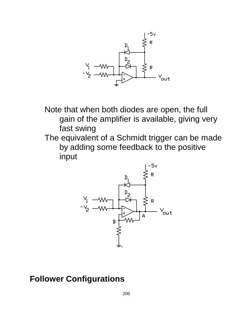
206
Note that when both diodes are open, the fullgain of the amplifier is available, giving veryfast swing
The equivalent of a Schmidt trigger can be madeby adding some feedback to the positiveinput
Follower Configurations

VP'R1
R1%R
2
Vout
Vin'VP
Vout'(1%R2
R1
)Vin
207
It is possible to use op-amp in non-invertingconfiguration
The "follower" ...
The voltage at P is
Because of infinit gain, + and - input voltagesmust be approximately equal,
Solving,
Advantages of this configuration

Vout'Vin
208
it doesn’t invert!very high input impedance (ideally infinite)
Disadvantagesnot functionally flexible (because of "1")doesn’t sum
Voltage Follower
Remove R (i.e., infinite resistance)1
Input/output equation becomes
This is more than a wireIdeally, it has infinite input impedance (draws no
current)Zero output inpedance (maintains voltage
regardless of current drawn)It will isolate output from inputUsed as first stage amplifier on instruments that
are low power, but not super low Peak Holder

209
Some nonlinear circuits can be built in follwerconfiguration
This is a peak holder
Capacitor will retain highest voltage it has seenDiode will open if input voltage drops below
capacitor voltageAdd a switch around capacitor for resetSimilar result can be obtained with just diode and
capacitorProblems with passive circuit
diode dropcapacitor current comes from input device
Op-amp gain solves both these problemsHigh input impedanceDiode drop is divided by amplifier gain
Digital to Analog Converters
Summation type converter

210
Major problem - wide range of resistor values4000:1 for 12-bit converterDifficult to get right valuesCould go out of range of op-ampDifferent temperature sensitivity make it hard to
calibrate Ladder Network for D/A
Ladder network solves these problems
Only two resistor values used, R and 2ROp-amp is used in follower configurationInput forms a resitor divider network with V as+

211
the take-off pointFor example, with input at 100(binary) (as
shown)Network is
So V is 1/2 of input (reference)+
Functional Characteristics
Open loop gain:10 (80 db) for standard (industrial) grade4
10 (100 db) for readily available amps5
10 (120 db) for specialty (expensive) amps6
gain(db) = 20 log (gain)10
Input impedance:transistor input - 300K to 3M (Ohms)Darlington - 1 to 10MFET input - 100M to 1,000G
Output impedancetypically 150-200 Ohmsrange can be 10 Ohms to 5K Ohms
Input offset voltageGenerated when amplifier inputs are grounded
212
Consumer grade - 10 mVIndustrial grade - 3 mVMilitary grade - 1 mVFET-types - 10 Xs as large
Not a big problem except in systems withintegrators
Bandwidth
GBP - gain x bandwidth productBandwidth defined as the frequency at which the
gain drops by 3 dbGBP is typically 1 - 10MHzFor example, GBP of 5MHz, gain of 10 gives5
bandwidth of only 50 HzNot serious problem, however, as long as gain
stays high enough for infinite gainassumption to hold