MDT - ozQRP.com MDT Block Diagram ... TX mode it mixes the VFO carrier signal with the microphone...
42
MDT Construction Manual – Issue 2 Page 1 MDT DSB TRANSCEIVER CONSTRUCTION MANUAL
Transcript of MDT - ozQRP.com MDT Block Diagram ... TX mode it mixes the VFO carrier signal with the microphone...
MDT Construction Manual – Issue 2 Page 1
MDT DSB TRANSCEIVER
CONSTRUCTION MANUAL
MDT Construction Manual – Issue 2 Page 2
CONTENTS
1 Introduction .............................................................................................................................................................. 4
2 DSB vs SSB ................................................................................................................................................................. 5
3 DSB transmitter ....................................................................................................................................................... 6
4 Direct Conversion receiver ................................................................................................................................. 7
5 MDT Block Diagram ............................................................................................................................................... 8
6 Circuit Description ................................................................................................................................................. 9
6.1 Variable Frequency Oscillator (VFO) ........................................................................................................................ 9
6.2 Mixer ....................................................................................................................................................................................... 9
6.3 Microphone amplifier ................................................................................................................................................... 10
6.4 Transmit amplifier ......................................................................................................................................................... 10
6.5 Power Supply and RX/TX switching ...................................................................................................................... 11
6.6 Receive audio .................................................................................................................................................................... 11
7 Kit Supplied Parts ................................................................................................................................................ 17
8 Individual Parts List ............................................................................................................................................ 19
9 Construction ........................................................................................................................................................... 21
9.1 General ................................................................................................................................................................................ 21
9.2 Building the PCB.............................................................................................................................................................. 22
10 Final Assembly ...................................................................................................................................................... 33
10.1 Microphone socket ......................................................................................................................................................... 33
10.2 Terminating plugs .......................................................................................................................................................... 34
10.3 Front Panel ........................................................................................................................................................................ 35
10.4 Mounting the PCB ........................................................................................................................................................... 35
11 Testing and alignment ....................................................................................................................................... 36
11.1 General ................................................................................................................................................................................ 36
11.2 Power on ............................................................................................................................................................................. 36
11.3 Receive ................................................................................................................................................................................ 36
11.4 Transmit ............................................................................................................................................................................. 37
11.5 Marking the VFO scale .................................................................................................................................................. 38
12 Modifications ......................................................................................................................................................... 40
12.1 Setting the VFO range ................................................................................................................................................... 40
12.2 Receiver alignment ........................................................................................................................................................ 40
12.3 Crystal operation ............................................................................................................................................................ 40
12.4 Using a loudspeaker ...................................................................................................................................................... 40
13 Operation................................................................................................................................................................. 41
13.1 Setting up ........................................................................................................................................................................... 41
13.2 Receiving ............................................................................................................................................................................ 41
13.2.1 SSB .......................................................................................................................................................... 41
13.2.2 CW ........................................................................................................................................................... 41
13.3 Transmitting ..................................................................................................................................................................... 42
MDT Construction Manual – Issue 2 Page 3
List of Figures
Figure 1 DSB generation ................................................................................................................................................ 6
Figure 2 Direct Conversion receiver ......................................................................................................................... 7
Figure 3 MDT Block diagram ....................................................................................................................................... 8
Figure 4 Carrier oscillator .......................................................................................................................................... 12
Figure 5 Mixer ................................................................................................................................................................. 13
Figure 6 Microphone Amplifier ............................................................................................................................... 14
Figure 7 Transmit .......................................................................................................................................................... 15
Figure 8 Receive Audio ................................................................................................................................................ 16
Figure 9 Diode identification .................................................................................................................................... 22
Figure 10 DIP ICs ........................................................................................................................................................... 23
Figure 11 Relay install ................................................................................................................................................. 23
Figure 12 Non-polarised capacitors ...................................................................................................................... 24
Figure 13 LPF capacitor marking ............................................................................................................................ 24
Figure 14 Trimcap install ........................................................................................................................................... 25
Figure 15 BD139 location .......................................................................................................................................... 25
Figure 16 BD139 lead identification ...................................................................................................................... 26
Figure 17 LED lead bending ...................................................................................................................................... 27
Figure 18 LED install .................................................................................................................................................... 27
Figure 19 Pot with tab removed .............................................................................................................................. 31
Figure 20 Component overlay .................................................................................................................................. 32
Figure 21 Mic connector wiring .............................................................................................................................. 33
Figure 22 Typical circuit voltages. .......................................................................................................................... 39
Figure 23 DSB transmit waveform ......................................................................................................................... 42
Change History Date Issue Comments
12-6-15 1 First release 20-6-15 2 Corrected values for R43 and C13, and other minor typos.
MDT Construction Manual – Issue 2 Page 4
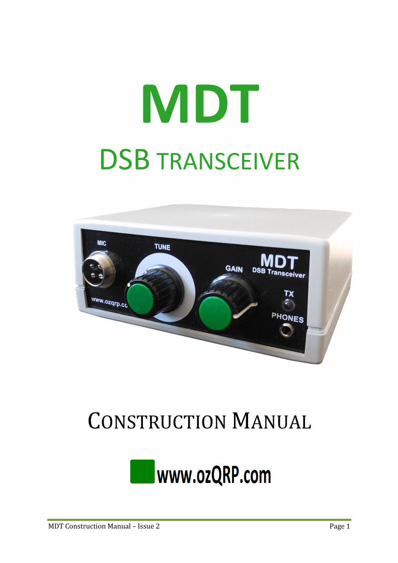
1 INTRODUCTION The MDT (Minimalist Double Sideband Transceiver) is an inexpensive and easy to build kit for the 40M band. It is ideal for the first time builder as all parts except the microphone socket are mounted on a single PCB and all the components are through hole. There is a SMD tuning diode but this comes pre-installed. The PCB is a high quality double sided type with ground plane, solder mask and silk screen. The plastic case is small and lightweight and can easily be held in one hand. The front and rear panels, which are made of PCB material, come pre-cut and feature silkscreened labeling. The low receive current of the MDT means it is ideal for battery operation. The transmitter outputs between 1.5 and 2 watts DSB which is ample for short distance contacts through the day and long distance contacts under good conditions. DSB transmissions are entirely compatible with SSB transceivers, and in fact most operators won’t be aware unless you tell them. Building the MDT is quick and easy. The receiver doesn’t require any alignment and the only setup required for the transmitter is setting the microphone gain and balancing the mixer to null out the carrier. A kit of parts for the MDT including everything you need, such as enclosure and front and rear
panels is available from www.ozQRP.com.
MDT Specifications and features:
1. Size 130mm x 100mm x 50mm.
2. Direct Conversion receiver. Sensitivity 0.4uV for 10dB S+N/N.
3. Double Sideband transmitter. Nominal 1.5W output. Up to 2W depending on power
supply voltage.
4. Selectable frequency range. 7.090MHz - 7.130MHz or 7.050MHz - 7.110MHz.
5. Microphone amplifier accepts standard low impedance dynamic or Electret microphone
with selectable on-board bias resistor.
6. LED transmit power and modulation indicator.
7. 3.5mm stereo headphone connector. Can power external loudspeaker.
8. Carrier suppression up to 50dB.
9. All spurious transmit outputs better than -46dBC.
10. Receive current approximately 50mA.
11. Transmit current approximately 250mA at maximum power output.
12. Reverse polarity protection using a series-diode.

MDT Construction Manual – Issue 2 Page 5
2 DSB VS SSB Why DSB? The answer is simple. A DSB transceiver is less expensive, less complicated and
easier to build and align than a SSB transceiver. This is due mainly to a DSB transceiver not
having a crystal filter, IF amplifier and multiple mixers that are required in a SSB design. Note
that in a DSB transceiver the receiver is more often referred to as a Direct Conversion (DC)
receiver.
For the first time builder or for a small and cheap rig, DSB is ideal. Over the years countless
amateurs have started out this way.
While a DSB rig has many advantages for the home builder, there are some things to consider.
Firstly, a DSB transmitter occupies twice the bandwidth of a SSB transmitter. On a quiet band
this does not cause any problems but on a crowded band it may not be as easy to find a free spot
to operate without interfering with nearby stations. Secondly, the Direct Conversion receiver
has equal response to both sidebands. This means you hear signals on both upper and lower
sidebands simultaneously. This results in a slightly higher noise level and the possibility of
hearing two separate stations at the same time.
There are, however, a couple of nice advantages when a Direct Conversion receiver is used with
a DSB transmitter. Firstly, you can operate with SSB stations using Upper Sideband (USB) or
Lower Sideband (LSB) without having to change controls or move frequency. Secondly, being
able to hear both sidebands means that you can check for other stations on both sides of your
frequency before transmitting and avoid interfering with them.
MDT Construction Manual – Issue 2 Page 6
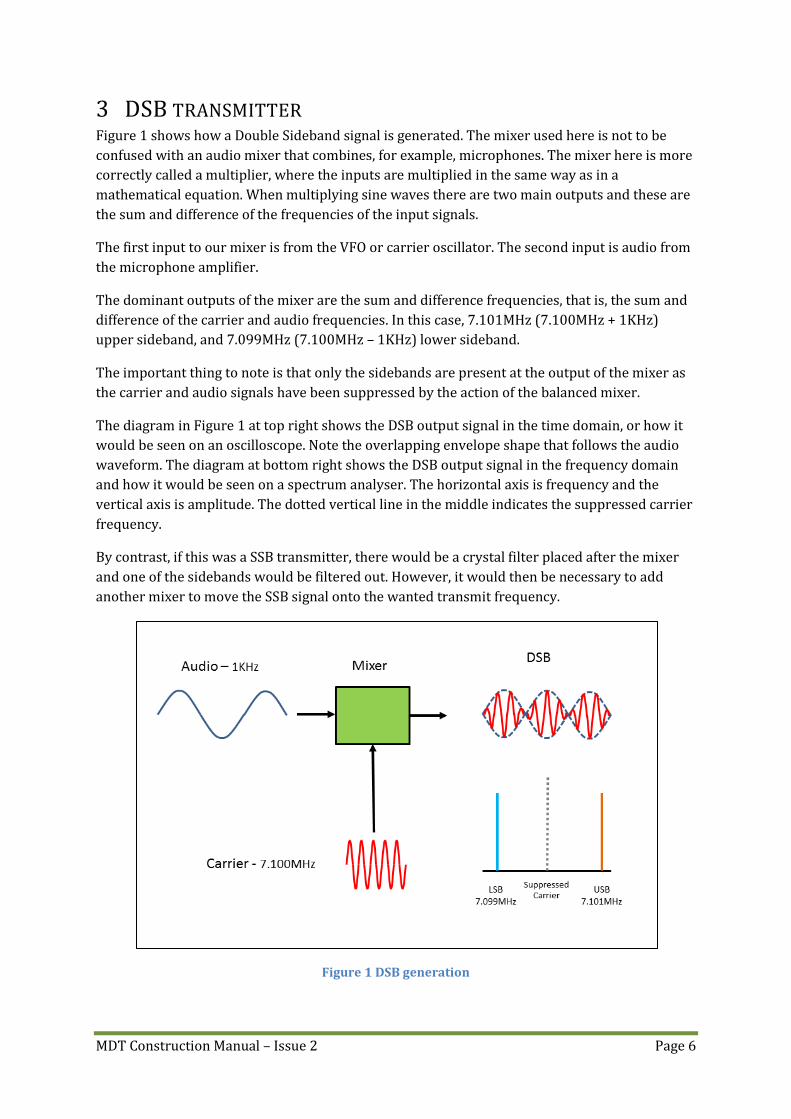
3 DSB TRANSMITTER Figure 1 shows how a Double Sideband signal is generated. The mixer used here is not to be
confused with an audio mixer that combines, for example, microphones. The mixer here is more
correctly called a multiplier, where the inputs are multiplied in the same way as in a
mathematical equation. When multiplying sine waves there are two main outputs and these are
the sum and difference of the frequencies of the input signals.
The first input to our mixer is from the VFO or carrier oscillator. The second input is audio from
the microphone amplifier.
The dominant outputs of the mixer are the sum and difference frequencies, that is, the sum and
difference of the carrier and audio frequencies. In this case, 7.101MHz (7.100MHz + 1KHz)
upper sideband, and 7.099MHz (7.100MHz – 1KHz) lower sideband.
The important thing to note is that only the sidebands are present at the output of the mixer as
the carrier and audio signals have been suppressed by the action of the balanced mixer.
The diagram in Figure 1 at top right shows the DSB output signal in the time domain, or how it
would be seen on an oscilloscope. Note the overlapping envelope shape that follows the audio
waveform. The diagram at bottom right shows the DSB output signal in the frequency domain
and how it would be seen on a spectrum analyser. The horizontal axis is frequency and the
vertical axis is amplitude. The dotted vertical line in the middle indicates the suppressed carrier
frequency.
By contrast, if this was a SSB transmitter, there would be a crystal filter placed after the mixer
and one of the sidebands would be filtered out. However, it would then be necessary to add
another mixer to move the SSB signal onto the wanted transmit frequency.
Figure 1 DSB generation
MDT Construction Manual – Issue 2 Page 7
4 DIRECT CONVERSION RECEIVER Figure 2 shows the simplified diagram of a Direct Conversion receiver. As with a DSB generator
the mixer has two inputs and an output, but this time the signal directions are reversed.
Signals from the antenna are presented to the mixer, and mixed with the VFO signal. The output
again contains sum and difference signals. The sum frequency of 7.101MHz + 7.100MHz
(14.201MHz) is easily filtered out by a low pass audio filter. However the difference frequency
of 7.101MHz – 7.100MHz (1KHz) can pass through the filter and be heard in the headphones.
This is the upper sideband response as the antenna signal frequency of 7.101MHz is above the
7.100MHz VFO frequency.
Note that there is also another antenna signal that can be heard. This is the lower sideband
signal at 7.099MHz. This would also produce a 1KHz tone in the headphones.
This ability to simultaneously detect both upper and lower sidebands is an important
characteristic of a Direct Conversion receiver.
Both Figure 1 and Figure 2 show a single 1KHz tone for the audio signal. This is done to make it
easier to understand the process involved. In practice there would be a range of voice band
frequencies present, but the same mixing conversion principle applies.
Figure 2 Direct Conversion receiver
MDT Construction Manual – Issue 2 Page 8
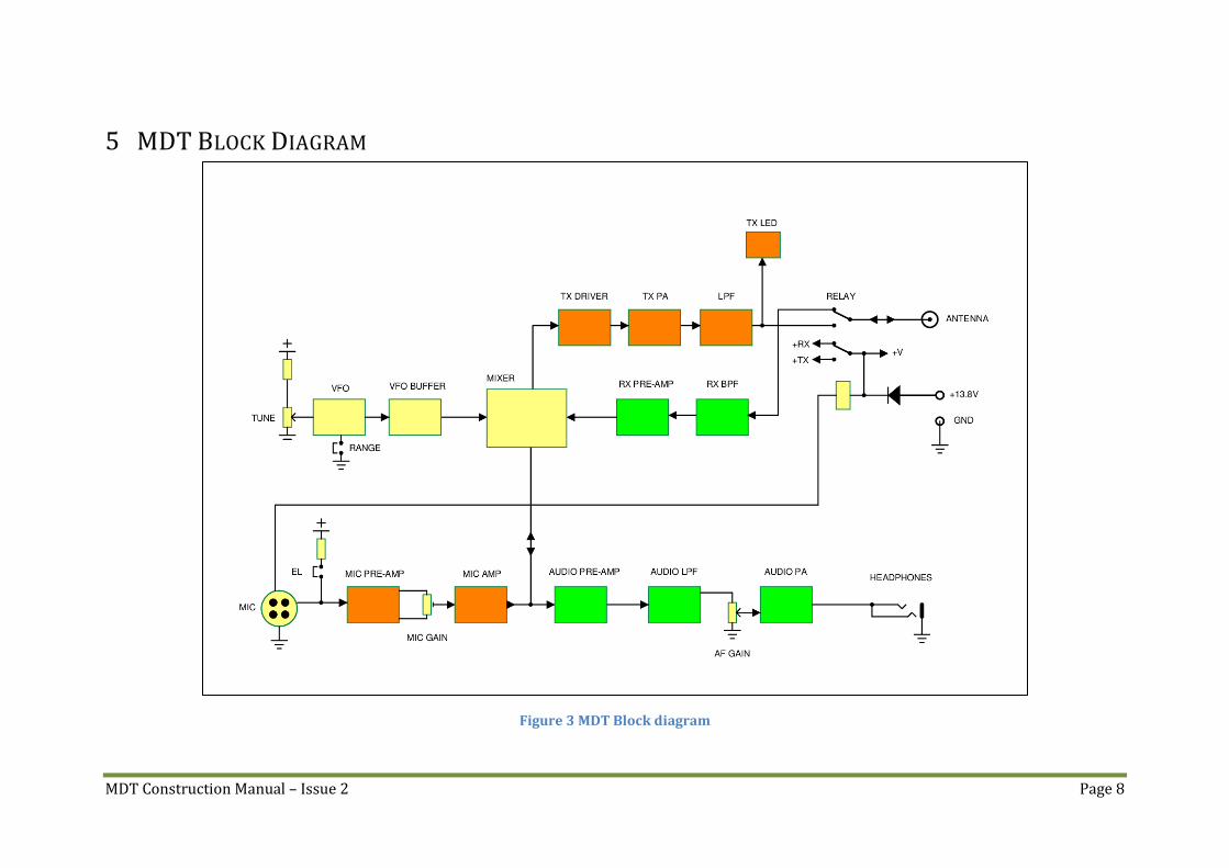
5 MDT BLOCK DIAGRAM
Figure 3 MDT Block diagram

MDT Construction Manual – Issue 2 Page 9
6 CIRCUIT DESCRIPTION
6.1 VARIABLE FREQUENCY OSCILLATOR (VFO) Transistor Q1 is configured as a Colpitts oscillator and acts as the carrier oscillator in transmit
and beat frequency oscillator (BFO) in receive. The frequency is set predominantly by a ceramic
resonator (X1) and a dual variable capacitance (varicap) diode D1. The capacitance of D1 is
altered by a varying the DC voltage applied to the Cathodes through the Tune control VR1 and
R3. To help stabilize the oscillator and minimize frequency drift the power supply to the
oscillator and the Tune control is regulated with a 9.1V Zener diode ZD1.
The VFO has effectively two ranges through the Range link. If the link is closed both varicap
diodes are in parallel circuit and the tuning range is approximately 60KHz. With the link open,
only one varicap diode is in use and the range change is reduced to around 40KHz. Capacitor C3
is not normally used.
The oscillator signal is fed to the emitter follower buffer stage Q2 via a small capacitor (C6). The
buffer stage provides light loading of the oscillator and a low impedance drive for the mixer.
6.2 MIXER The balanced mixer is a diode switching type and doubly balanced. It performs two functions. In
TX mode it mixes the VFO carrier signal with the microphone audio signal to produce DSB while
in RX mode it mixes the antenna signal with the VFO signal to produce received audio.
The carrier signal, which is much larger in amplitude than the audio signal, is applied
simultaneously to both sides of the mixer through trimpot VR2. The carrier signal turns on the
diodes to form a low resistance and is why it is referred to as a switching mixer. As the carrier is
capacitively coupled it swings both positive and negative around ground potential. When the
carrier is positive, current flows through diodes D2 and D5 causing them to conduct and
become a low resistance. When the carrier goes negative diodes D3 and D4 conduct. Note that
capacitor C10 holds the junction of D2 and D4 at ground for RF. As the currents are equal
through each of the conducting diodes the differential voltage across winding one of T1 does not
change and no RF is present at winding three, the output of T1. If an audio signal is injected into
the bridge at the junction of D2 and D4 the mixer balance is upset because the audio changes
state much less frequently than the carrier signal and the instantaneous diode currents are not
equal. As a result a signal is now output on winding three of T1, which is a double sideband
suppressed carrier waveform.
Due to variations in component parameters the mixer balance is not exact and if not
compensated for the carrier balance would be poor. Trimmer capacitor TC1 and C9 are used to
equalize the capacitance on the mixer sides, while trimpot VR2 is used to balance the diode
currents in each side. They are adjusted together to bring the modulator into balance. In
practice up to 50dB of carrier suppression can be achieved.
MDT Construction Manual – Issue 2 Page 10
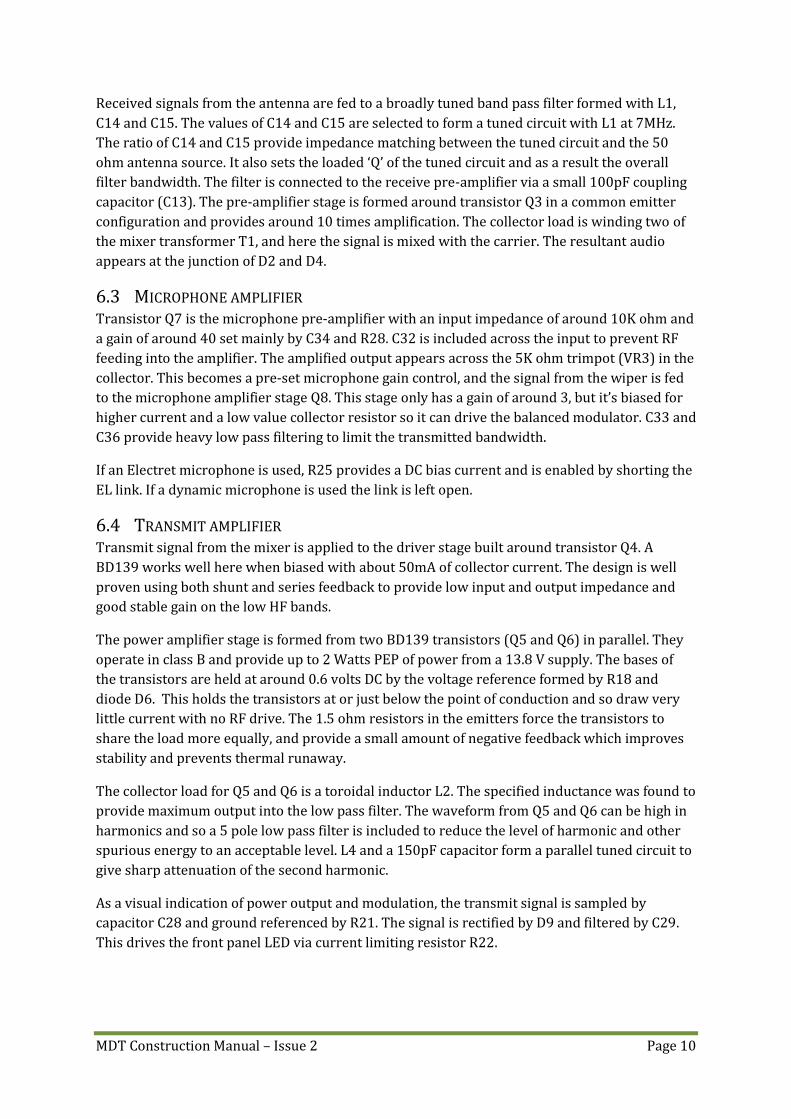
Received signals from the antenna are fed to a broadly tuned band pass filter formed with L1,
C14 and C15. The values of C14 and C15 are selected to form a tuned circuit with L1 at 7MHz.
The ratio of C14 and C15 provide impedance matching between the tuned circuit and the 50
ohm antenna source. It also sets the loaded ‘Q’ of the tuned circuit and as a result the overall
filter bandwidth. The filter is connected to the receive pre-amplifier via a small 100pF coupling
capacitor (C13). The pre-amplifier stage is formed around transistor Q3 in a common emitter
configuration and provides around 10 times amplification. The collector load is winding two of
the mixer transformer T1, and here the signal is mixed with the carrier. The resultant audio
appears at the junction of D2 and D4.
6.3 MICROPHONE AMPLIFIER Transistor Q7 is the microphone pre-amplifier with an input impedance of around 10K ohm and
a gain of around 40 set mainly by C34 and R28. C32 is included across the input to prevent RF
feeding into the amplifier. The amplified output appears across the 5K ohm trimpot (VR3) in the
collector. This becomes a pre-set microphone gain control, and the signal from the wiper is fed
to the microphone amplifier stage Q8. This stage only has a gain of around 3, but it’s biased for
higher current and a low value collector resistor so it can drive the balanced modulator. C33 and
C36 provide heavy low pass filtering to limit the transmitted bandwidth.
If an Electret microphone is used, R25 provides a DC bias current and is enabled by shorting the
EL link. If a dynamic microphone is used the link is left open.
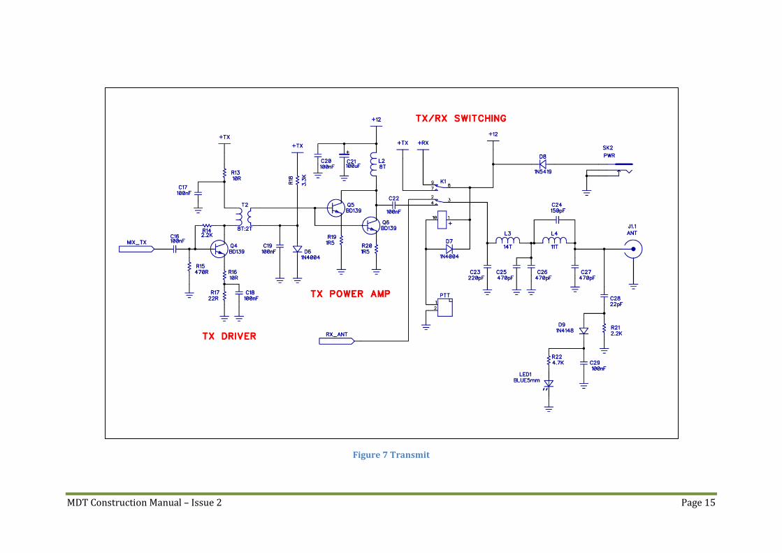
6.4 TRANSMIT AMPLIFIER Transmit signal from the mixer is applied to the driver stage built around transistor Q4. A
BD139 works well here when biased with about 50mA of collector current. The design is well
proven using both shunt and series feedback to provide low input and output impedance and
good stable gain on the low HF bands.
The power amplifier stage is formed from two BD139 transistors (Q5 and Q6) in parallel. They
operate in class B and provide up to 2 Watts PEP of power from a 13.8 V supply. The bases of
the transistors are held at around 0.6 volts DC by the voltage reference formed by R18 and
diode D6. This holds the transistors at or just below the point of conduction and so draw very
little current with no RF drive. The 1.5 ohm resistors in the emitters force the transistors to
share the load more equally, and provide a small amount of negative feedback which improves
stability and prevents thermal runaway.
The collector load for Q5 and Q6 is a toroidal inductor L2. The specified inductance was found to
provide maximum output into the low pass filter. The waveform from Q5 and Q6 can be high in
harmonics and so a 5 pole low pass filter is included to reduce the level of harmonic and other
spurious energy to an acceptable level. L4 and a 150pF capacitor form a parallel tuned circuit to
give sharp attenuation of the second harmonic.
As a visual indication of power output and modulation, the transmit signal is sampled by
capacitor C28 and ground referenced by R21. The signal is rectified by D9 and filtered by C29.
This drives the front panel LED via current limiting resistor R22.
MDT Construction Manual – Issue 2 Page 11
6.5 POWER SUPPLY AND RX/TX SWITCHING When the PTT is operated the TX/RX relay is energized and the transmit signal is passed to the
antenna. When the PTT is not operated the relay switches the antenna through to the receive
circuits. The relay also switches power to the TX and RX sections as required
Diode D8 provides reverse polarity protection. With the power supply connected with the right
polarity, D8 will pass current onto the board. There is a small voltage drop of about 0.3 volts but
this has minimal effect on transmitter performance. If the supply is connected in reverse D8
will not conduct and the board will be protected.
6.6 RECEIVE AUDIO The low level audio signal from the mixer is applied to the audio pre-amplifier stage (U1A). This
is formed from one half of an LM833 dual low noise op-amp and has a gain of around 100 or
40dB. A reference supply for the non-inverting input is obtained from R33, R35 and C40. The
high frequency response of U1A is limited by C41. The output of U1A is DC coupled to the 2 pole
low pass filter (U1B) with a 3dB cutoff frequency of 2400Hz. This stage has only unity gain but
its main task is to set the receiver bandwidth.
The output of the low pass filter is coupled to the AF gain control VR4 via a 1uF capacitor (C44).
A LM386 (U2) is used to boost the signal from the AF gain control to drive a set of headphones.
The gain is set by C47 and R42 to about 50 times or 34dB, while resistor R43 limits the audio to
a comfortable level for headphone listening. If an external low impedance speaker is used
instead of headphones, then R43 can be replaced with a link.
A MOSFET (Q9) is turned on in TX mode and shorts the audio signal to ground. Even though the
audio amplifiers are switched off during transmit, this is still necessary because microphone
signals can make their way through to the headphones while the audio amplifiers are turning
off.
MDT Construction Manual – Issue 2 Page 12
Figure 4 Carrier oscillator
MDT Construction Manual – Issue 2 Page 13
Figure 5 Mixer
MDT Construction Manual – Issue 2 Page 14
Figure 6 Microphone Amplifier
MDT Construction Manual – Issue 2 Page 15
Figure 7 Transmit

MDT Construction Manual – Issue 2 Page 16
Figure 8 Receive Audio
MDT Construction Manual – Issue 2 Page 17
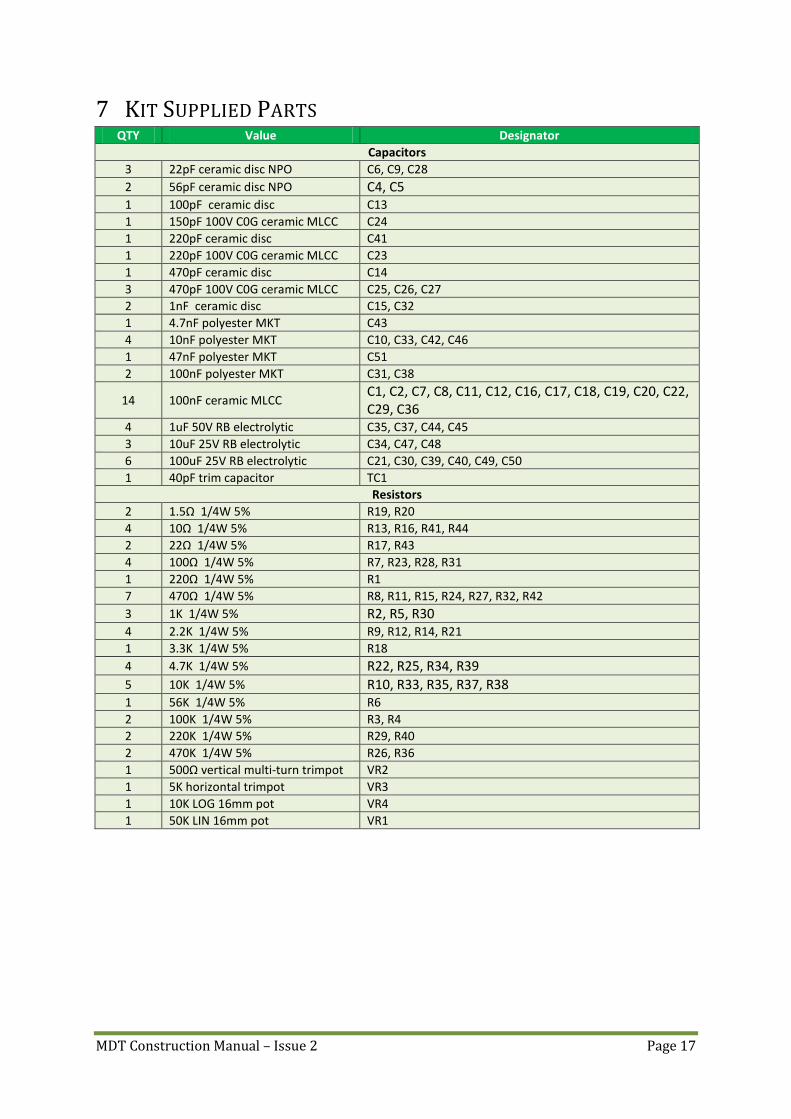
7 KIT SUPPLIED PARTS QTY Value Designator
Capacitors
3 22pF ceramic disc NPO C6, C9, C28
2 56pF ceramic disc NPO C4, C5 1 100pF ceramic disc C13
1 150pF 100V C0G ceramic MLCC C24
1 220pF ceramic disc C41
1 220pF 100V C0G ceramic MLCC C23
1 470pF ceramic disc C14
3 470pF 100V C0G ceramic MLCC C25, C26, C27
2 1nF ceramic disc C15, C32
1 4.7nF polyester MKT C43
4 10nF polyester MKT C10, C33, C42, C46
1 47nF polyester MKT C51
2 100nF polyester MKT C31, C38
14 100nF ceramic MLCC C1, C2, C7, C8, C11, C12, C16, C17, C18, C19, C20, C22, C29, C36
4 1uF 50V RB electrolytic C35, C37, C44, C45
3 10uF 25V RB electrolytic C34, C47, C48
6 100uF 25V RB electrolytic C21, C30, C39, C40, C49, C50
1 40pF trim capacitor TC1
Resistors
2 1.5Ω 1/4W 5% R19, R20
4 10Ω 1/4W 5% R13, R16, R41, R44
2 22Ω 1/4W 5% R17, R43
4 100Ω 1/4W 5% R7, R23, R28, R31
1 220Ω 1/4W 5% R1
7 470Ω 1/4W 5% R8, R11, R15, R24, R27, R32, R42
3 1K 1/4W 5% R2, R5, R30
4 2.2K 1/4W 5% R9, R12, R14, R21
1 3.3K 1/4W 5% R18
4 4.7K 1/4W 5% R22, R25, R34, R39
5 10K 1/4W 5% R10, R33, R35, R37, R38
1 56K 1/4W 5% R6
2 100K 1/4W 5% R3, R4
2 220K 1/4W 5% R29, R40
2 470K 1/4W 5% R26, R36
1 500Ω vertical multi-turn trimpot VR2
1 5K horizontal trimpot VR3
1 10K LOG 16mm pot VR4
1 50K LIN 16mm pot VR1
MDT Construction Manual – Issue 2 Page 18
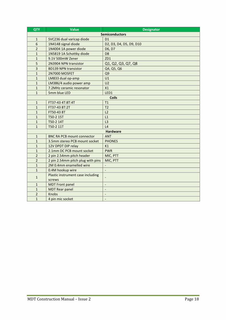
QTY Value Designator
Semiconductors
1 SVC236 dual varicap diode D1
6 1N4148 signal diode D2, D3, D4, D5, D9, D10
2 1N4004 1A power diode D6, D7
1 1N5819 1A Schottky diode D8
1 9.1V 500mW Zener ZD1
5 2N3904 NPN transistor Q1, Q2, Q3, Q7, Q8
3 BD139 NPN transistor Q4, Q5, Q6
1 2N7000 MOSFET Q9
1 LM833 dual op-amp U1
1 LM386/4 audio power amp U2
1 7.2MHz ceramic resonator X1
1 5mm blue LED LED1
Coils
1 FT37-43 4T:8T:4T T1
1 FT37-43 8T:2T T2
1 FT50-43 8T L2
1 T50-2 15T L1
1 T50-2 14T L3
1 T50-2 11T L4
Hardware
1 BNC RA PCB mount connector ANT
1 3.5mm stereo PCB mount socket PHONES
1 12V DPDT DIP relay K1
1 2.1mm DC PCB mount socket PWR
2 2 pin 2.54mm pitch header MIC, PTT
2 2 pin 2.54mm pitch plug with pins MIC, PTT
1 2M 0.4mm enamelled wire -
1 0.4M hookup wire -
1 Plastic instrument case including screws
-
1 MDT Front panel -
1 MDT Rear panel -
2 Knobs -
1 4 pin mic socket -
MDT Construction Manual – Issue 2 Page 19
8 INDIVIDUAL PARTS LIST
Desig. Value Type Desig. Value Type
ANT - PCB mount RA BNC C44 1uF 50V RB electrolytic
C45 1uF 50V RB electrolytic
C1 100nF ceramic MLCC C46 10nF polyester MKT
C2 100nF ceramic MLCC C47 10uF 25V RB electrolytic
C3 - Not used. See text C48 10uF 25V RB electrolytic
C4 56pF ceramic disc NPO C49 100uF 25V RB electrolytic
C5 56pF ceramic disc NPO C50 100uF 25V RB electrolytic
C6 22pF ceramic disc NPO C51 47nF polyester MKT
C7 100nF ceramic MLCC
C8 100nF ceramic MLCC D1 SVC236 Dual Varicap
C9 22pF ceramic disc NPO D2 1N4148 Signal diode
C10 10nF polyester MKT D3 1N4148 Signal diode
C11 100nF ceramic MLCC D4 1N4148 Signal diode
C12 100nF ceramic MLCC D5 1N4148 Signal diode
C13 100pF ceramic disc NPO D6 1N4004 1A power diode
C14 470pF ceramic disc D7 1N4004 1A power diode
C15 1nF ceramic disc D8 1N5819 1A Schottky diode
C16 100nF ceramic MLCC D9 1N4148 Signal diode
C17 100nF ceramic MLCC D10 1N4148 Signal diode
C18 100nF ceramic MLCC
C19 100nF ceramic MLCC K1 - PCB mount DIP signal relay
C20 100nF ceramic MLCC
C21 100uF 25V RB electrolytic L1 15T T50-2 toroid
C22 100nF ceramic MLCC L2 8T FT50-43 toroid
C23 220pF 100V C0G ceramic MLCC L3 14T T50-2 toroid
C24 150pF 100V C0G ceramic MLCC L4 11T T50-2 toroid
C25 470pF 100V C0G ceramic MLCC LED1 - 5mm Blue LED
C26 470pF 100V C0G ceramic MLCC
C27 470pF 100V C0G ceramic MLCC MIC - 2 pin vertical header
C28 22pF ceramic disc NPO
C29 100nF ceramic MLCC PHONES - PCB mount 3.5mm stereo socket
C30 100uF 25V RB electrolytic PWR - PCB mount 2.1mm DC socket
C31 100nF polyester MKT PTT - 2 pin vertical header
C32 1nF ceramic disc
C33 10nF polyester MKT Q1 2N3904 NPN transistor
C34 10uF 25V RB electrolytic Q2 2N3904 NPN transistor
C35 1uF 50V RB electrolytic Q3 2N3904 NPN transistor
C36 100nF ceramic MLCC Q4 BD139 NPN transistor
C37 1uF 50V RB electrolytic Q5 BD139 NPN transistor
C38 100nF polyester MKT Q6 BD139 NPN transistor
C39 100uF 25V RB electrolytic Q7 2N3904 NPN transistor
C40 100uF 25V RB electrolytic Q8 2N3904 NPN transistor
C41 220pF ceramic disc Q9 2N7000 N ch MOSFET
C42 10nF polyester MKT
C43 4.7nF polyester MKT
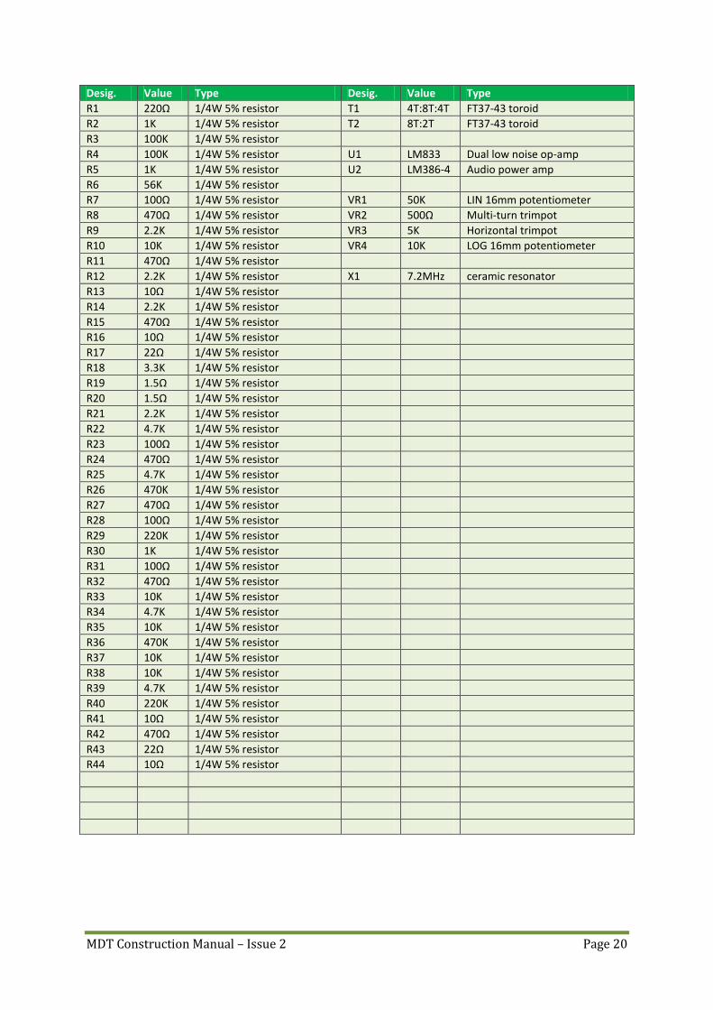
MDT Construction Manual – Issue 2 Page 20
Desig. Value Type Desig. Value Type
R1 220Ω 1/4W 5% resistor T1 4T:8T:4T FT37-43 toroid
R2 1K 1/4W 5% resistor T2 8T:2T FT37-43 toroid
R3 100K 1/4W 5% resistor
R4 100K 1/4W 5% resistor U1 LM833 Dual low noise op-amp
R5 1K 1/4W 5% resistor U2 LM386-4 Audio power amp
R6 56K 1/4W 5% resistor
R7 100Ω 1/4W 5% resistor VR1 50K LIN 16mm potentiometer
R8 470Ω 1/4W 5% resistor VR2 500Ω Multi-turn trimpot
R9 2.2K 1/4W 5% resistor VR3 5K Horizontal trimpot
R10 10K 1/4W 5% resistor VR4 10K LOG 16mm potentiometer
R11 470Ω 1/4W 5% resistor
R12 2.2K 1/4W 5% resistor X1 7.2MHz ceramic resonator
R13 10Ω 1/4W 5% resistor
R14 2.2K 1/4W 5% resistor
R15 470Ω 1/4W 5% resistor
R16 10Ω 1/4W 5% resistor
R17 22Ω 1/4W 5% resistor
R18 3.3K 1/4W 5% resistor
R19 1.5Ω 1/4W 5% resistor
R20 1.5Ω 1/4W 5% resistor
R21 2.2K 1/4W 5% resistor
R22 4.7K 1/4W 5% resistor
R23 100Ω 1/4W 5% resistor
R24 470Ω 1/4W 5% resistor
R25 4.7K 1/4W 5% resistor
R26 470K 1/4W 5% resistor
R27 470Ω 1/4W 5% resistor
R28 100Ω 1/4W 5% resistor
R29 220K 1/4W 5% resistor
R30 1K 1/4W 5% resistor
R31 100Ω 1/4W 5% resistor
R32 470Ω 1/4W 5% resistor
R33 10K 1/4W 5% resistor
R34 4.7K 1/4W 5% resistor
R35 10K 1/4W 5% resistor
R36 470K 1/4W 5% resistor
R37 10K 1/4W 5% resistor
R38 10K 1/4W 5% resistor
R39 4.7K 1/4W 5% resistor
R40 220K 1/4W 5% resistor
R41 10Ω 1/4W 5% resistor
R42 470Ω 1/4W 5% resistor
R43 22Ω 1/4W 5% resistor
R44 10Ω 1/4W 5% resistor
MDT Construction Manual – Issue 2 Page 21
9 CONSTRUCTION
9.1 GENERAL The MDT is built on a high quality fiberglass PCB. The PCB is doubled sided with the majority of
the tracks on the bottom side with the top side forming a ground plane.
To assist construction the component overlay is screen printed on the top side and a solder
mask is included to help guard against solder bridges.
The ground plane is substantial and can sink quite a bit of heat from low wattage soldering irons
so ensure you use a good quality iron that can sustain the power required. You may find that
sometimes solder doesn’t appear to flow through to the top side. This is not necessarily a
problem because the plated through holes make a connection to the top side automatically.
Another point to consider is that plated through holes consume more solder than non-plated
holes and makes it more difficult to remove components. So check the value and orientation of
components before soldering!
There isn’t a ‘best’ scheme for loading the components. If desired you can build sections at a
time and test them out, but it is not really necessary and in any case some sections rely on
others before they will operate. The suggested procedure is to load the smaller components and
those closest to the PCB first and then work upwards.
MDT Construction Manual – Issue 2 Page 22
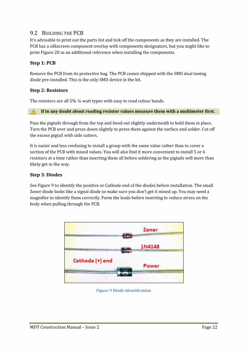
9.2 BUILDING THE PCB It’s advisable to print out the parts list and tick off the components as they are installed. The
PCB has a silkscreen component overlay with components designators, but you might like to
print Figure 20 as an additional reference when installing the components.
Step 1: PCB
Remove the PCB from its protective bag. The PCB comes shipped with the SMD dual tuning
diode pre-installed. This is the only SMD device in the kit.
Step 2: Resistors
The resistors are all 5% ¼ watt types with easy to read colour bands.
If in any doubt about reading resistor values measure them with a multimeter first.
Pass the pigtails through from the top and bend out slightly underneath to hold them in place.
Turn the PCB over and press down slightly to press them against the surface and solder. Cut off
the excess pigtail with side cutters.
It is easier and less confusing to install a group with the same value rather than to cover a
section of the PCB with mixed values. You will also find it more convenient to install 5 or 6
resistors at a time rather than inserting them all before soldering as the pigtails will more than
likely get in the way.
Step 3: Diodes
See Figure 9 to identify the positive or Cathode end of the diodes before installation. The small
Zener diode looks like a signal diode so make sure you don’t get it mixed up. You may need a
magnifier to identify them correctly. Form the leads before inserting to reduce stress on the
body when pulling through the PCB.
Figure 9 Diode identification
MDT Construction Manual – Issue 2 Page 23
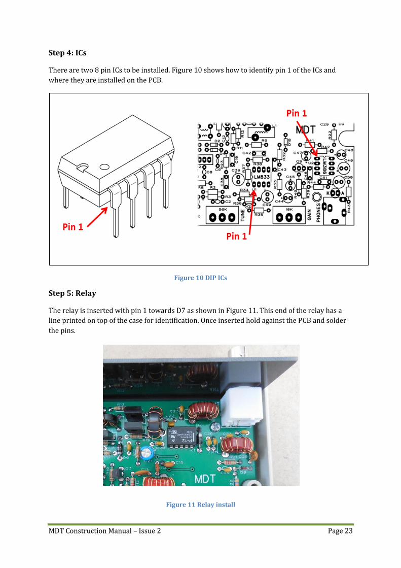
Step 4: ICs
There are two 8 pin ICs to be installed. Figure 10 shows how to identify pin 1 of the ICs and
where they are installed on the PCB.
Figure 10 DIP ICs
Step 5: Relay
The relay is inserted with pin 1 towards D7 as shown in Figure 11. This end of the relay has a
line printed on top of the case for identification. Once inserted hold against the PCB and solder
the pins.
Figure 11 Relay install
MDT Construction Manual – Issue 2 Page 24
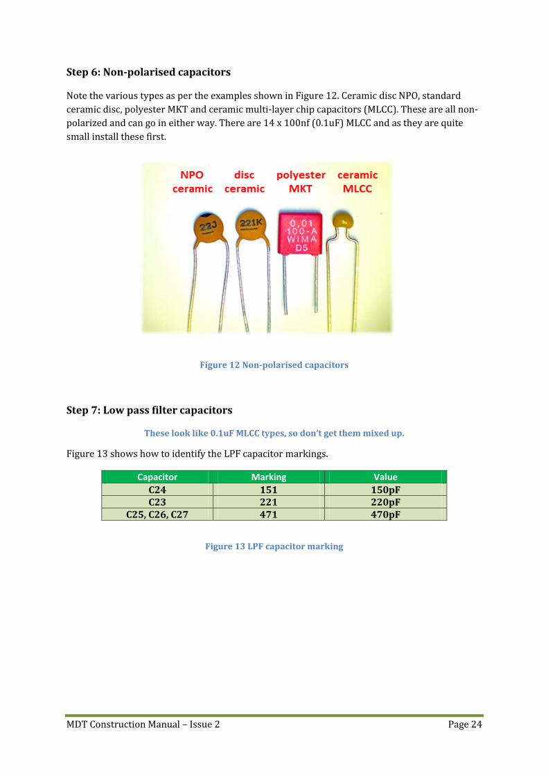
Step 6: Non-polarised capacitors
Note the various types as per the examples shown in Figure 12. Ceramic disc NPO, standard
ceramic disc, polyester MKT and ceramic multi-layer chip capacitors (MLCC). These are all non-
polarized and can go in either way. There are 14 x 100nf (0.1uF) MLCC and as they are quite
small install these first.
Figure 12 Non-polarised capacitors
Step 7: Low pass filter capacitors
These look like 0.1uF MLCC types, so don’t get them mixed up.
Figure 13 shows how to identify the LPF capacitor markings.
Capacitor Marking Value
C24 151 150pF C23 221 220pF
C25, C26, C27 471 470pF
Figure 13 LPF capacitor marking
MDT Construction Manual – Issue 2 Page 25
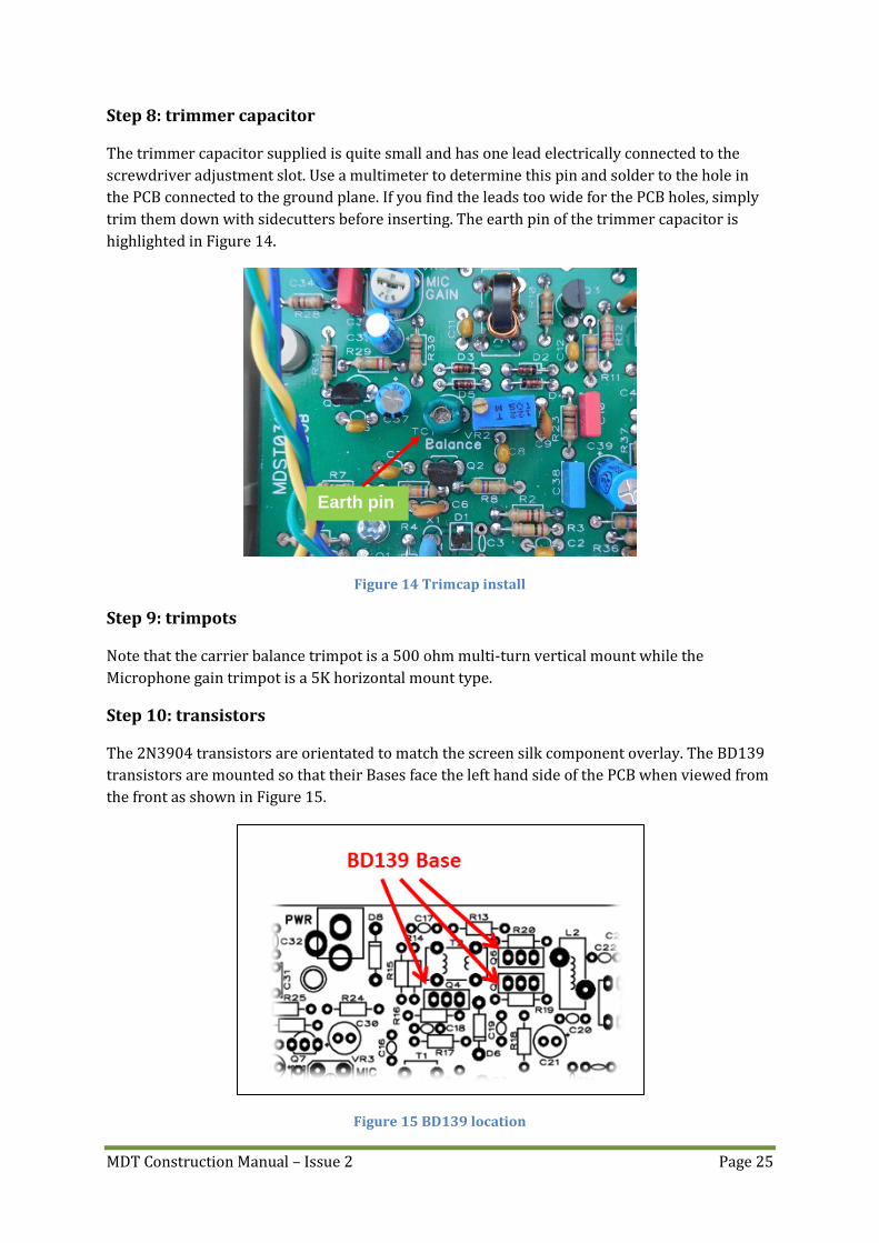
Step 8: trimmer capacitor
The trimmer capacitor supplied is quite small and has one lead electrically connected to the
screwdriver adjustment slot. Use a multimeter to determine this pin and solder to the hole in
the PCB connected to the ground plane. If you find the leads too wide for the PCB holes, simply
trim them down with sidecutters before inserting. The earth pin of the trimmer capacitor is
highlighted in Figure 14.
Figure 14 Trimcap install
Step 9: trimpots
Note that the carrier balance trimpot is a 500 ohm multi-turn vertical mount while the
Microphone gain trimpot is a 5K horizontal mount type.
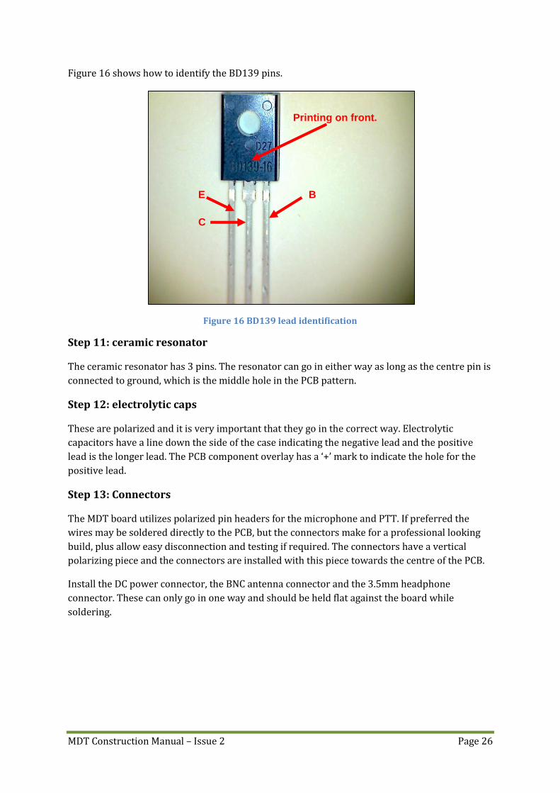
Step 10: transistors
The 2N3904 transistors are orientated to match the screen silk component overlay. The BD139
transistors are mounted so that their Bases face the left hand side of the PCB when viewed from
the front as shown in Figure 15.
Figure 15 BD139 location
Earth pin
MDT Construction Manual – Issue 2 Page 26
Figure 16 shows how to identify the BD139 pins.
Figure 16 BD139 lead identification
Step 11: ceramic resonator
The ceramic resonator has 3 pins. The resonator can go in either way as long as the centre pin is
connected to ground, which is the middle hole in the PCB pattern.
Step 12: electrolytic caps
These are polarized and it is very important that they go in the correct way. Electrolytic
capacitors have a line down the side of the case indicating the negative lead and the positive
lead is the longer lead. The PCB component overlay has a ‘+’ mark to indicate the hole for the
positive lead.
Step 13: Connectors
The MDT board utilizes polarized pin headers for the microphone and PTT. If preferred the
wires may be soldered directly to the PCB, but the connectors make for a professional looking
build, plus allow easy disconnection and testing if required. The connectors have a vertical
polarizing piece and the connectors are installed with this piece towards the centre of the PCB.
Install the DC power connector, the BNC antenna connector and the 3.5mm headphone
connector. These can only go in one way and should be held flat against the board while
soldering.
E
C
B
Printing on front.
MDT Construction Manual – Issue 2 Page 27
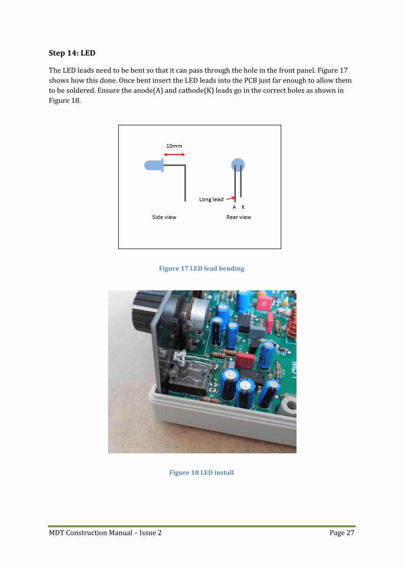
Step 14: LED
The LED leads need to be bent so that it can pass through the hole in the front panel. Figure 17
shows how this done. Once bent insert the LED leads into the PCB just far enough to allow them
to be soldered. Ensure the anode(A) and cathode(K) leads go in the correct holes as shown in
Figure 18.
Figure 17 LED lead bending
Figure 18 LED install

MDT Construction Manual – Issue 2 Page 28
Step 15: Coils
Count turns on the inside of the toroid. A turn is considered to be counted when a wire passes
through the center hole.
Transformer T1 Take a 120 mm length of 0.4mm enamelled copper wire. Wind 4 turns on a FT37-43 ferrite toroid. This is winding 1. Take a 180 mm length of 0.4mm enamelled copper wire. Wind 8 turns on the ferrite toroid. This is winding 2. Take a 120 mm length of 0.4mm enamelled copper wire. Wind 4 turns on the ferrite toroid. This is winding 3. Scrape the enamel off the ends of the wires and tin with solder before installing in the PCB. The winding direction is not important.
Transformers T2 Take a 180mm length of 0.4mm enamelled copper wire and wind the 8 turn primary on a FT37-43 ferrite toroid. Take a 90mm length of 0.4mm enamelled copper wire and wind the 2 turn secondary. Scrape the enamel off the ends of the wires and tin with solder before installing in the PCB. The winding direction is not important.
MDT Construction Manual – Issue 2 Page 29
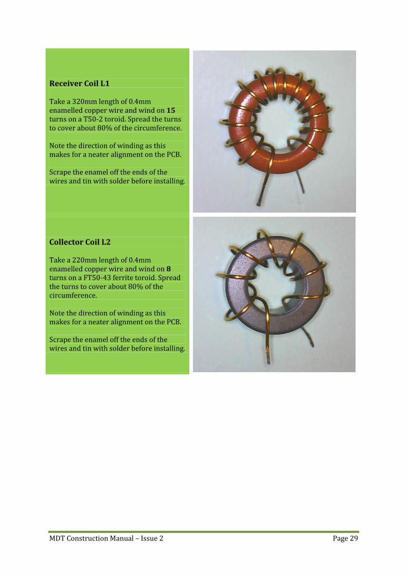
Receiver Coil L1 Take a 320mm length of 0.4mm enamelled copper wire and wind on 15 turns on a T50-2 toroid. Spread the turns to cover about 80% of the circumference. Note the direction of winding as this makes for a neater alignment on the PCB. Scrape the enamel off the ends of the wires and tin with solder before installing.
Collector Coil L2 Take a 220mm length of 0.4mm enamelled copper wire and wind on 8 turns on a FT50-43 ferrite toroid. Spread the turns to cover about 80% of the circumference. Note the direction of winding as this makes for a neater alignment on the PCB. Scrape the enamel off the ends of the wires and tin with solder before installing.
MDT Construction Manual – Issue 2 Page 30
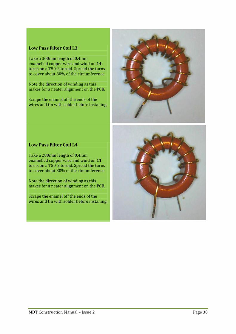
Low Pass Filter Coil L3 Take a 300mm length of 0.4mm enamelled copper wire and wind on 14 turns on a T50-2 toroid. Spread the turns to cover about 80% of the circumference. Note the direction of winding as this makes for a neater alignment on the PCB. Scrape the enamel off the ends of the wires and tin with solder before installing.
Low Pass Filter Coil L4 Take a 280mm length of 0.4mm enamelled copper wire and wind on 11 turns on a T50-2 toroid. Spread the turns to cover about 80% of the circumference. Note the direction of winding as this makes for a neater alignment on the PCB. Scrape the enamel off the ends of the wires and tin with solder before installing.
MDT Construction Manual – Issue 2 Page 31
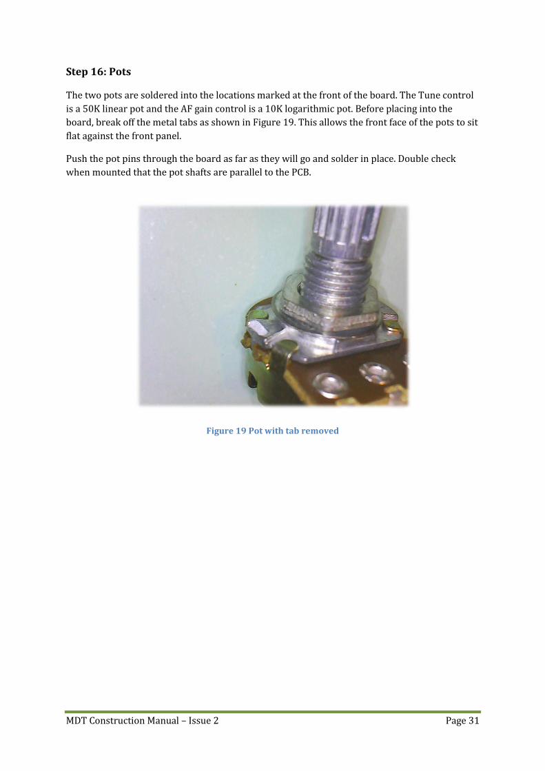
Step 16: Pots
The two pots are soldered into the locations marked at the front of the board. The Tune control
is a 50K linear pot and the AF gain control is a 10K logarithmic pot. Before placing into the
board, break off the metal tabs as shown in Figure 19. This allows the front face of the pots to sit
flat against the front panel.
Push the pot pins through the board as far as they will go and solder in place. Double check
when mounted that the pot shafts are parallel to the PCB.
Figure 19 Pot with tab removed

MDT Construction Manual – Issue 2 Page 32
Figure 20 Component overlay
MDT Construction Manual – Issue 2 Page 33
10 FINAL ASSEMBLY Before installing the board in the enclosure, carefully look for errors, such as components in the
wrong way and solder bridges between tracks. The risk of solder bridges is greatly reduced due
to the solder mask, but check anyway. A few moments spent here is cheap insurance against big
problems later on.
One of the more common problems is poor solder joints with enamel covered wire. Some types
when soldered will easily melt the enamel but most will not, so it is important to scrape the
enamel off the ends of the wires with sandpaper or a sharp knife before soldering.
The enclosure comes with two plastic panels. These are not required and can be set aside for
some other use. In this kit they are replaced with pre-cut and printed front and rear panels.
These are actually made from PCB material with a black solder mask and white silkscreen
lettering. The front panel has a white circle placed around the Tune control to allow marking
frequency steps with a pen - more on this later.
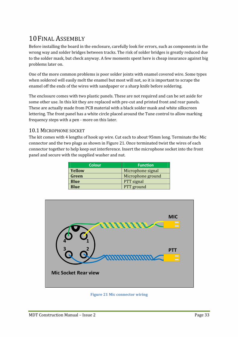
10.1 MICROPHONE SOCKET The kit comes with 4 lengths of hook up wire. Cut each to about 95mm long. Terminate the Mic
connector and the two plugs as shown in Figure 21. Once terminated twist the wires of each
connector together to help keep out interference. Insert the microphone socket into the front
panel and secure with the supplied washer and nut.
Colour Function
Yellow Microphone signal Green Microphone ground Blue PTT signal Blue PTT ground
Figure 21 Mic connector wiring
MDT Construction Manual – Issue 2 Page 34
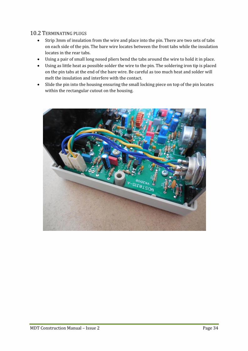
10.2 TERMINATING PLUGS Strip 3mm of insulation from the wire and place into the pin. There are two sets of tabs
on each side of the pin. The bare wire locates between the front tabs while the insulation
locates in the rear tabs.
Using a pair of small long nosed pliers bend the tabs around the wire to hold it in place.
Using as little heat as possible solder the wire to the pin. The soldering iron tip is placed
on the pin tabs at the end of the bare wire. Be careful as too much heat and solder will
melt the insulation and interfere with the contact.
Slide the pin into the housing ensuring the small locking piece on top of the pin locates
within the rectangular cutout on the housing.
MDT Construction Manual – Issue 2 Page 35
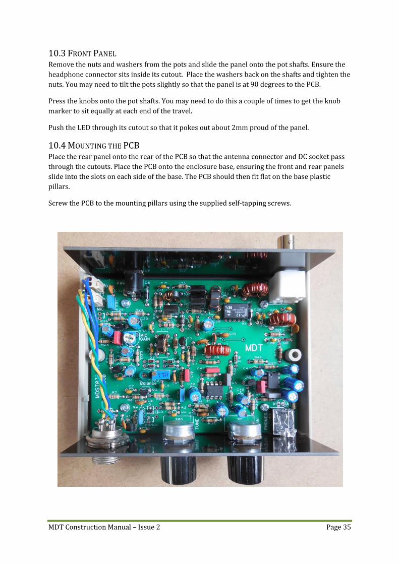
10.3 FRONT PANEL Remove the nuts and washers from the pots and slide the panel onto the pot shafts. Ensure the
headphone connector sits inside its cutout. Place the washers back on the shafts and tighten the
nuts. You may need to tilt the pots slightly so that the panel is at 90 degrees to the PCB.
Press the knobs onto the pot shafts. You may need to do this a couple of times to get the knob
marker to sit equally at each end of the travel.
Push the LED through its cutout so that it pokes out about 2mm proud of the panel.
10.4 MOUNTING THE PCB Place the rear panel onto the rear of the PCB so that the antenna connector and DC socket pass
through the cutouts. Place the PCB onto the enclosure base, ensuring the front and rear panels
slide into the slots on each side of the base. The PCB should then fit flat on the base plastic
pillars.
Screw the PCB to the mounting pillars using the supplied self-tapping screws.

MDT Construction Manual – Issue 2 Page 36
11 TESTING AND ALIGNMENT
11.1 GENERAL The minimum tools and accessories needed to get the MDT tested and aligned are listed below:
Digital multimeter.
50 ohm dummy load capable of dissipating at least 2 Watts.
Power supply capable of 13.8V DC regulated at 1 Amp.
A second receiver.
Small adjustment screwdriver.
These additional instruments are recommended to fully test and align the MDT.
QRP wattmeter or oscilloscope
An audio signal generator.
An RF signal generator.
A frequency counter.
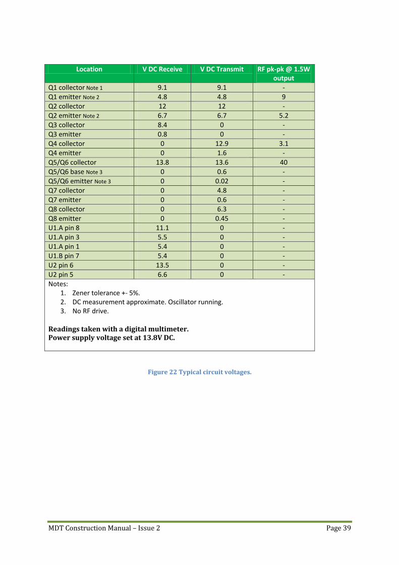
Figure 22 lists typical voltages at various points around the board and can be used to verify operation.
11.2 POWER ON Connect a 50 Ohm dummy load to the antenna socket.
Connect the power supply to the DC connector.
If your power supply does not include a current meter, connect a multimeter in series
with the power supply positive lead and set to measure current.
Turn on the power supply and note the supply current. It should be around 50mA. If it’s
far from this turn off immediately and look for problems.
The relay should be de-energized and the board in RX mode. To verify that there are no
obvious problems do a quick probe around the board with a multimeter and check the
DC receive voltages as shown in Figure 22.
11.3 RECEIVE Set the Tune control to around the middle of the range.
Turn the AF gain control to halfway. You should hear some low level hiss come from the
headphones indicating that the audio stages are working.
Remove the dummy load and apply a RF signal of about 100uV to the antenna connector
and rotate the Tune control until a clear tone is heard in the headphones.
If no signal is heard check the receive circuit.
If you don’t have a signal generator simply plug in an antenna and listen. You will get a
good idea if the receiver is working correctly by comparing to another receiver.
MDT Construction Manual – Issue 2 Page 37
11.4 TRANSMIT Remove the RF signal source and reconnect the dummy load. It is suggested you have
some way of measuring the power output. A QRP power meter or oscilloscope would be
ideal.
Turn the Mic gain trimpot VR3 fully counter-clockwise.
Briefly switch to TX mode by shorting the PTT contacts. Check the power supply current.
If the mixer is already balanced there will be no output and the current and should rise
to about 130mA. If the mixer is not balanced there may be RF output and the current
may be higher. If it is way in excess of 250mA this indicates a problem and should be
investigated.
Place a short across the PTT line. Adjust carrier balance controls TC1 and VR2 for
minimum power output. Initially you can use the LED indicator to monitor this, but as
the mixer reaches balance the output power will decrease significantly and the LED will
not turn on. At this point it’s necessary to use some other way to monitor the power
output to do the final balancing. The following are some suggested methods:
o Using a second receiver placed nearby listen to the transmitted signal. Ensure
you are not listening to the VFO signal as this is on the same frequency.
o Connect an oscilloscope across the dummy load.
o Connect a sensitive RF probe across the dummy load.
o Connect a spectrum analyser across the dummy load. An attenuator may be
necessary.
In all cases it’s simply a matter of monitoring the transmitted signal for minimum output
while adjusting TC1 and VR2. The carrier null is quite sharp, and there is some
interaction between the controls, so you will need to go back and forwards to obtain
maximum balance.
Check the TX mode DC voltages as shown in Figure 22. If there are any off scale readings
turn off immediately and look for construction errors.
Remove the short across the PTT line. Apply an audio signal generator to the Mic socket
set to 1KHz at around 50mV. Operate the PTT again and slowly rotate the Mic gain
trimpot clockwise while monitoring the power output. The power output should
increase smoothly without any sudden dips or surges and you should be able to easily
achieve 1.5 to 2 Watts output. At this level the front panel LED should be brightly lit.
Remove the signal generator and check that the RF output goes to zero, and the LED
turns off.
If you intend to use an Electret microphone place a short across the EL link. This can be
a soldered link or you can install a 2 pin header and a removable shunt. Leave the link
open for dynamic microphones.
Plug in a microphone and check the relay operates when the PTT is pressed. When you
speak there should be RF output, and the LED should flash. You will now be able to
monitor yourself with a receiver placed nearby and determine an appropriate Mic gain
setting.
MDT Construction Manual – Issue 2 Page 38
11.5 MARKING THE VFO SCALE The VFO dial on the front panel comes without any markings. The reason for this is that the
frequency range will be slightly different for each kit due to variations in component values and
the selected frequency range etc. There are many ways to mark the scale, but following is an
easy and simple method:
Ensure the MDT has been powered on for at least 10 minutes to allow the VFO section to
warm up and stabilize. This is especially important if any of the VFO components have
been recently soldered.
Connect a frequency counter across R8.
Rotate the Tune control fully anti-clockwise. Read and note the frequency on the
counter.
Rotate the Tune control fully clockwise. Read and note the frequency on the counter.
From the two readings determine what markings you wish to make on the scale. Marks
at every 10KHz would be a convenient option.
Start at the low frequency end of the tuning range and while monitoring the counter
rotate the Tune control until you reach a 10KHz point. For example 7.060MHz.
Make a mark on the scale at the knob pointer line. A fine point felt marker is ideal.
Rotate the Tune control until you reach the next 10KHz point. For example 7.070MHz
and make a mark.
Repeat the process across the tuning range.
MDT Construction Manual – Issue 2 Page 39
Location V DC Receive V DC Transmit RF pk-pk @ 1.5W output
Q1 collector Note 1 9.1 9.1 -
Q1 emitter Note 2 4.8 4.8 9
Q2 collector 12 12 -
Q2 emitter Note 2 6.7 6.7 5.2
Q3 collector 8.4 0 -
Q3 emitter 0.8 0 -
Q4 collector 0 12.9 3.1
Q4 emitter 0 1.6 -
Q5/Q6 collector 13.8 13.6 40
Q5/Q6 base Note 3 0 0.6 -
Q5/Q6 emitter Note 3 0 0.02 -
Q7 collector 0 4.8 -
Q7 emitter 0 0.6 -
Q8 collector 0 6.3 -
Q8 emitter 0 0.45 -
U1.A pin 8 11.1 0 -
U1.A pin 3 5.5 0 -
U1.A pin 1 5.4 0 -
U1.B pin 7 5.4 0 -
U2 pin 6 13.5 0 -
U2 pin 5 6.6 0 -
Notes: 1. Zener tolerance +- 5%. 2. DC measurement approximate. Oscillator running. 3. No RF drive.
Readings taken with a digital multimeter. Power supply voltage set at 13.8V DC.
Figure 22 Typical circuit voltages.
MDT Construction Manual – Issue 2 Page 40
12 MODIFICATIONS
12.1 SETTING THE VFO RANGE The VFO tuning range is reasonably fixed due to the characteristics of the ceramic resonator and
the available capacitance swing of the varicap but it can be adjusted slightly if required.
The Range link. With the link shorted the two varicap diodes are in parallel and the
tuning range is approximately 7.050MHz to 7.110MHz. With the link open only one
varicap diode is in circuit and the tuning range becomes approximately 7.090MHz to
7.130MHz.
Resistor R2. Increasing the value of R2 will lower the maximum voltage across the Tune
control and will in turn decrease the tuning range and maximum frequency of the VFO.
Capacitor C3. This isn’t included in the parts list, but adding a small value NPO ceramic
here will lower the overall frequency range.
12.2 RECEIVER ALIGNMENT The tuned circuit at the front end of the receiver containing coil L4 is designed for a bandpass
wide enough to cover the 40M band without adjustment. If it is necessary for some reason to
alter the tuned circuit frequency then this will require a change in the turns on L4.
If, however, only a small adjustment is required this can be done by compressing or spreading
the turns on L4. Nominally the turns should be evenly spaced over about 80% of the
circumference. However if the turns are compressed the inductance will increase slightly and
lower the tuned circuit frequency. Conversely, if the turns are separated the inductance will
decrease slightly and the frequency will increase. To check the frequency of the modified tuned
circuit do the following:
Inject a stable signal into the antenna socket in the middle of the tuning range.
Rotate the Tune control until a clean tone is heard in the headphones, and adjust the AF
gain control for a comfortable level.
Place an audio level meter or oscilloscope across the AF gain control and monitor the
amplitude of the audio tone for maximum while spreading and compressing the turns on
L4.
When a maximum is reached the alignment is complete.
12.3 CRYSTAL OPERATION The MDT kit comes supplied with a 7.2MHz ceramic resonator which gives about 60KHz of
tuning range. This gives much better frequency stability than a conventional LC oscillator but is
not rock steady. If very stable frequency operation is required the resonator can be replaced
with a crystal. This is soldered into the outer resonator holes in the PCB. The centre earth hole is
ignored. The Tune control can then be used as a fine tune control with around 1KHz of
adjustment.
12.4 USING A LOUDSPEAKER If you wish to use an external loudspeaker with the MDT, it is necessary to replace the 22 ohm
resistor R43 with a wire link. Otherwise the speaker level will be greatly reduced.
MDT Construction Manual – Issue 2 Page 41
13 OPERATION The following sections describe how to set up and use the MDT.
13.1 SETTING UP 1. Connect the antenna. You will require a BNC male plug on the antenna cable. If your
antenna cable has another type of plug, you will need an adaptor.
2. Plug in headphones. The MDT is intended to be used with 32 ohm stereo headphones. It
can drive any type of headphones but they must use a 3.5mm stereo phono plug.
3. Plug in the microphone. The MDT kit comes with a 4 pin socket which is a type
commonly used on radio transceivers. If your microphone does not use this type of
connector, then you will have to either replace the plug or change the socket on the
MDT. If making changes remember that the audio line must be independent of the PTT
line, however a common earth is allowed.
4. Connect the power supply. The MDT is designed to operate from a 13.8V DC power
source. This can be a battery or a regulated DC power supply. Don’t be tempted to use an
unregulated plug pack as the AC hum will make its way into the audio sections. The
supply connection is via a 2.1mm DC socket on the rear of the MDT. The positive wire
goes to the centre pin and the negative wire goes to the outer barrel of the connector.
The MDT can operate down to around 10V, but the transmit power output will be
significantly reduced. A supply of 15V DC is the recommended maximum voltage to use.
13.2 RECEIVING
The VFO is a free running oscillator and there will be some drift after powering on as the components warm up. It is best to avoid transmitting until it stabilizes. This only takes a couple of minutes and any drift after this period is quite small.
13.2.1 SSB The Tune control is used to tune in stations. The MDT doesn’t have a fine tune control so you
need to adjust the control slowly and carefully to tune in correctly. As you move across a SSB
station you will find a spot where the voice becomes clear and sounds natural. This should
coincide with the VFO and the transmit station being on or very near the same frequency.
The AF gain is the only other MDT control. Always start with the control set low when tuning
around so that sudden or strong signals do not overload your ears. The MDT does not have
automatic gain control (AGC) to level out the audio from different stations, so you need to set
the AF gain to match the level of the signal you are tuned.
13.2.2 CW When tuning CW signals you can tune either side of the transmit frequency to listen in. Tuning
across the signal the tone frequency will decrease as you approach zero beat. Zero beat is where
the VFO frequency is the same as the station transmit frequency. At zero beat you will hear
nothing or at least a very low frequency thumping sound. As you tune away on the other side of
zero beat the tone frequency will increase. Simply adjust the Tune control for a pleasant
sounding tone. Sometimes if there is an interfering signal on one side, you can tune to the other
side and reduce the interference while still receiving the wanted station.
MDT Construction Manual – Issue 2 Page 42
13.3 TRANSMITTING
Do not transmit without a matched 40M antenna or 50 dummy load connected.
To transmit press the PTT button on your microphone and talk. The LED on the front panel will
flash as you speak. This provides an indication of the power output, as the current through the
LED, and therefore its brightness, is dependent on the peak RF output. If the LED is illuminated
at a constant level when talking, it indicates that you are driving the transmitter too hard and
causing clipping of the RF signal.
Overdriving will create distortion and excessive harmonic generation and must be avoided.
To check your signal you can either, connect the MDT to a dummy load and monitor yourself
with headphones on a nearby receiver, or have a friend that lives close by listen to your signal.
The idea is to increase the Mic gain progressively while the receiving station sweeps across your
transmission looking for distortion and unwanted spurious byproducts. Set the Mic gain control
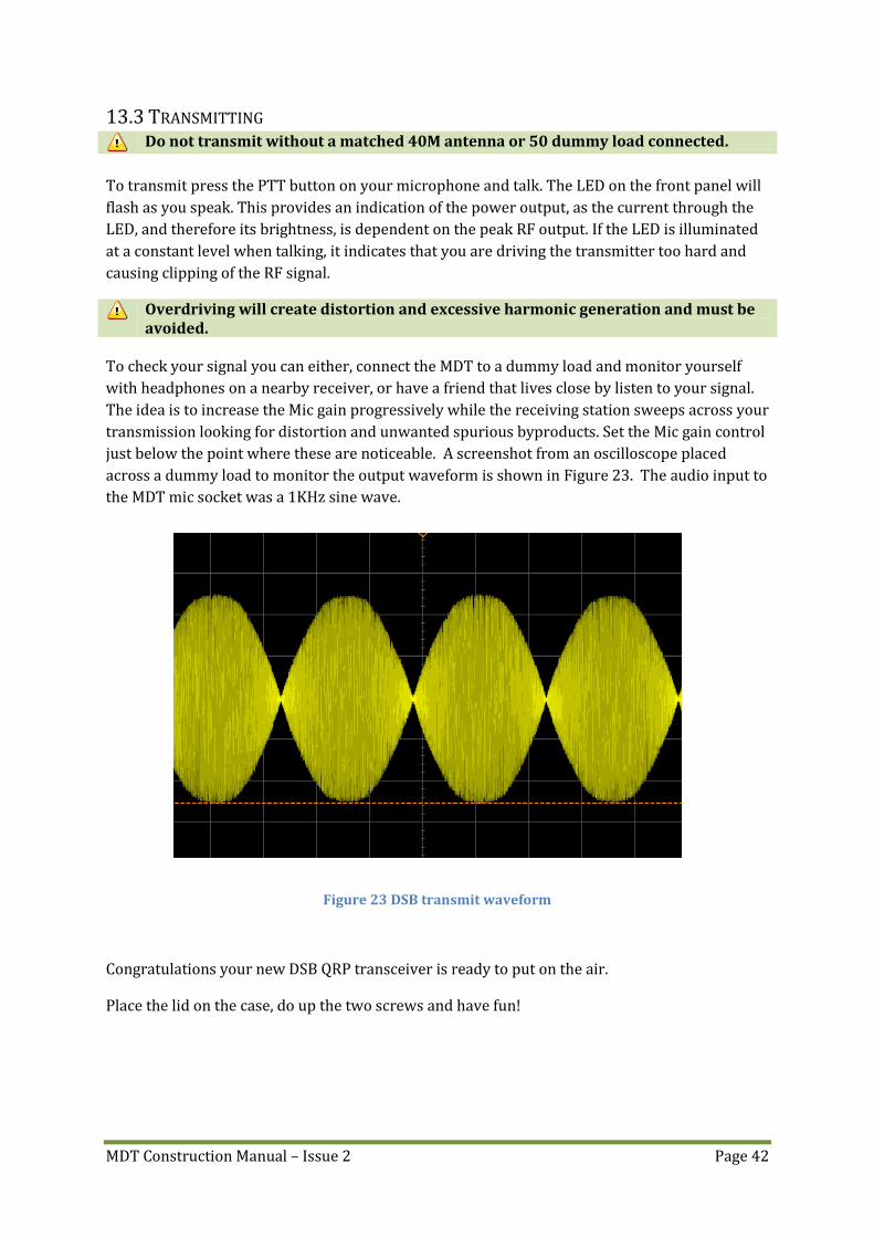
just below the point where these are noticeable. A screenshot from an oscilloscope placed
across a dummy load to monitor the output waveform is shown in Figure 23. The audio input to
the MDT mic socket was a 1KHz sine wave.
Figure 23 DSB transmit waveform
Congratulations your new DSB QRP transceiver is ready to put on the air.
Place the lid on the case, do up the two screws and have fun!