
MC68HC912BD32 Advance Information Rev 1.0 - Data Sheet
292
MC68HC912BD32/D MC68HC912BD32 Advance Information Rev 1.0 October 23, 2000 Freescale Semiconductor, I Freescale Semiconductor, Inc. For More Information On This Product, Go to: www.freescale.com nc...
Transcript of MC68HC912BD32 Advance Information Rev 1.0 - Data Sheet

Fre
esc
ale
Se
mic
on
du
cto
r, I
Freescale Semiconductor, Inc.n
c..
.
MC68HC912BD32/D
MC68HC912BD32Advance Information
Rev 1.0
October 23, 2000
For More Information On This Product,
Go to: www.freescale.com
RXZB30
logo
RXZB30
logo

F
ree
sca
le S
em
ico
nd
uc
tor,
I
Freescale Semiconductor, Inc.n
c..
.
For More Information On This Product,
Go to: www.freescale.com

Fre
esc
ale
Se
mic
on
du
cto
r, I
Freescale Semiconductor, Inc.n
c..
.
List of SectionsList of Sections
List of Sections . . . . . . . . . . . . . . . . . . . . . . . . . . . . . . . . . . 3
Table of Contents. . . . . . . . . . . . . . . . . . . . . . . . . . . . . . . . 1
General Description . . . . . . . . . . . . . . . . . . . . . . . . . . . . . 5
Central Processing Unit . . . . . . . . . . . . . . . . . . . . . . . . . . 11
Pinout and Signal Descriptions. . . . . . . . . . . . . . . . . . . . 17
Registers . . . . . . . . . . . . . . . . . . . . . . . . . . . . . . . . . . . . . . 33
Operating Modes and Resource Mapping. . . . . . . . . . 43
Bus Control and Input/Output . . . . . . . . . . . . . . . . . . . . 55
Flash EEPROM. . . . . . . . . . . . . . . . . . . . . . . . . . . . . . . . . . 65
EEPROM. . . . . . . . . . . . . . . . . . . . . . . . . . . . . . . . . . . . . . . 81
Resets and Interrupts. . . . . . . . . . . . . . . . . . . . . . . . . . . . 89
Clocks. . . . . . . . . . . . . . . . . . . . . . . . . . . . . . . . . . . . . . . . 97
Pulse Width Modulator . . . . . . . . . . . . . . . . . . . . . . . . . 109
Standard Timer Module. . . . . . . . . . . . . . . . . . . . . . . . . 127
Serial Interface. . . . . . . . . . . . . . . . . . . . . . . . . . . . . . . . 143
MC68HC912BD32 Rev 1.0
© Motorola, Inc., 1999List of Sections For More Information On This Product,
Go to: www.freescale.com

List of Sections
Fre
esc
ale
Se
mic
on
du
cto
r, I
Freescale Semiconductor, Inc.n
c..
.
Byteflight™ Module . . . . . . . . . . . . . . . . . . . . . . . . . . . . 167
Analog to Digital Converter . . . . . . . . . . . . . . . . . . . . . 219
Development Support . . . . . . . . . . . . . . . . . . . . . . . . . . 231
Preliminary Electrical Characteristics . . . . . . . . . . . . . 255
Literature Updates . . . . . . . . . . . . . . . . . . . . . . . . . . . . . 275
Glossary . . . . . . . . . . . . . . . . . . . . . . . . . . . . . . . . . . . . . 277
MC68HC912BD32 Rev 1.0
List of Sections For More Information On This Prod
Go to: www.freescale.com
uct,
Fre
esc
ale
Se
mic
on
du
cto
r, I
Freescale Semiconductor, Inc.n
c..
.
Table of ContentsTable of Contents
List of Sections
Table of Contents
General Description Contents . . . . . . . . . . . . . . . . . . . . . . . . . . . . . . . . . . . . . . . . . . . . . . . .5Introduction . . . . . . . . . . . . . . . . . . . . . . . . . . . . . . . . . . . . . . . . . . . . . .5Features . . . . . . . . . . . . . . . . . . . . . . . . . . . . . . . . . . . . . . . . . . . . . . . .6Ordering Information . . . . . . . . . . . . . . . . . . . . . . . . . . . . . . . . . . . . . . .8MC68HC912BD32 Block Diagram . . . . . . . . . . . . . . . . . . . . . . . . . . . .9
Central Processing Unit
Contents . . . . . . . . . . . . . . . . . . . . . . . . . . . . . . . . . . . . . . . . . . . . . . .11Introduction . . . . . . . . . . . . . . . . . . . . . . . . . . . . . . . . . . . . . . . . . . . . .11Programming Model . . . . . . . . . . . . . . . . . . . . . . . . . . . . . . . . . . . . . .11Data Types . . . . . . . . . . . . . . . . . . . . . . . . . . . . . . . . . . . . . . . . . . . . .13Addressing Modes . . . . . . . . . . . . . . . . . . . . . . . . . . . . . . . . . . . . . . .13Indexed Addressing Modes . . . . . . . . . . . . . . . . . . . . . . . . . . . . . . . .15Opcodes and Operands . . . . . . . . . . . . . . . . . . . . . . . . . . . . . . . . . . .16
Pinout and Signal Descriptions
Contents . . . . . . . . . . . . . . . . . . . . . . . . . . . . . . . . . . . . . . . . . . . . . . .17MC68HC912BD32 Rev 1.0 Pin Assignments . . . . . . . . . . . . . . . . . .17Power Supply Pins . . . . . . . . . . . . . . . . . . . . . . . . . . . . . . . . . . . . . . .19Signal Descriptions . . . . . . . . . . . . . . . . . . . . . . . . . . . . . . . . . . . . . . .20Port Signals . . . . . . . . . . . . . . . . . . . . . . . . . . . . . . . . . . . . . . . . . . . .26Port Pull-Up, Pull-Down and Reduced Drive . . . . . . . . . . . . . . . . . . .31
Registers Contents . . . . . . . . . . . . . . . . . . . . . . . . . . . . . . . . . . . . . . . . . . . . . . .33Introduction . . . . . . . . . . . . . . . . . . . . . . . . . . . . . . . . . . . . . . . . . . . . .33
Operating Modes and Resource Mapping
Contents . . . . . . . . . . . . . . . . . . . . . . . . . . . . . . . . . . . . . . . . . . . . . . .43Introduction . . . . . . . . . . . . . . . . . . . . . . . . . . . . . . . . . . . . . . . . . . . . .43Operating Modes . . . . . . . . . . . . . . . . . . . . . . . . . . . . . . . . . . . . . . . .43Background Debug Mode . . . . . . . . . . . . . . . . . . . . . . . . . . . . . . . . . .46Internal Resource Mapping . . . . . . . . . . . . . . . . . . . . . . . . . . . . . . . .49Memory Maps . . . . . . . . . . . . . . . . . . . . . . . . . . . . . . . . . . . . . . . . . . .53
MC68HC912BD32 Rev 1.0
Table of Contents For More Information On This Product,
Go to: www.freescale.com

Table of Contents
Fre
esc
ale
Se
mic
on
du
cto
r, I
Freescale Semiconductor, Inc.n
c..
.
Bus Control and Input/Output
Contents . . . . . . . . . . . . . . . . . . . . . . . . . . . . . . . . . . . . . . . . . . . . . . .55Introduction . . . . . . . . . . . . . . . . . . . . . . . . . . . . . . . . . . . . . . . . . . . . .55Detecting Access Type from External Signals . . . . . . . . . . . . . . . . . .55Registers . . . . . . . . . . . . . . . . . . . . . . . . . . . . . . . . . . . . . . . . . . . . . . .56
Flash EEPROM Contents . . . . . . . . . . . . . . . . . . . . . . . . . . . . . . . . . . . . . . . . . . . . . . .65Introduction . . . . . . . . . . . . . . . . . . . . . . . . . . . . . . . . . . . . . . . . . . . . .65Overview . . . . . . . . . . . . . . . . . . . . . . . . . . . . . . . . . . . . . . . . . . . . . . .66Flash EEPROM Control Block . . . . . . . . . . . . . . . . . . . . . . . . . . . . . .66Flash EEPROM Array . . . . . . . . . . . . . . . . . . . . . . . . . . . . . . . . . . . . .66Flash EEPROM Registers . . . . . . . . . . . . . . . . . . . . . . . . . . . . . . . . .67Operation . . . . . . . . . . . . . . . . . . . . . . . . . . . . . . . . . . . . . . . . . . . . . .71Programming the Flash EEPROM . . . . . . . . . . . . . . . . . . . . . . . . . . .74Erasing the Flash EEPROM . . . . . . . . . . . . . . . . . . . . . . . . . . . . . . . .76Program/Erase Protection Interlocks . . . . . . . . . . . . . . . . . . . . . . . . .78Stop or Wait Mode . . . . . . . . . . . . . . . . . . . . . . . . . . . . . . . . . . . . . . .78Test Mode . . . . . . . . . . . . . . . . . . . . . . . . . . . . . . . . . . . . . . . . . . . . . .79
EEPROM Contents . . . . . . . . . . . . . . . . . . . . . . . . . . . . . . . . . . . . . . . . . . . . . . .81Introduction . . . . . . . . . . . . . . . . . . . . . . . . . . . . . . . . . . . . . . . . . . . . .81EEPROM Programmer’s Model . . . . . . . . . . . . . . . . . . . . . . . . . . . . .82EEPROM Control Registers . . . . . . . . . . . . . . . . . . . . . . . . . . . . . . . .83
Resets and Interrupts
Contents . . . . . . . . . . . . . . . . . . . . . . . . . . . . . . . . . . . . . . . . . . . . . . .89Introduction . . . . . . . . . . . . . . . . . . . . . . . . . . . . . . . . . . . . . . . . . . . . .89Exception Priority . . . . . . . . . . . . . . . . . . . . . . . . . . . . . . . . . . . . . . . .89Maskable interrupts . . . . . . . . . . . . . . . . . . . . . . . . . . . . . . . . . . . . . .90Interrupt Control and Priority Registers . . . . . . . . . . . . . . . . . . . . . . .92Resets . . . . . . . . . . . . . . . . . . . . . . . . . . . . . . . . . . . . . . . . . . . . . . . . .93Effects of Reset . . . . . . . . . . . . . . . . . . . . . . . . . . . . . . . . . . . . . . . . .94Register Stacking . . . . . . . . . . . . . . . . . . . . . . . . . . . . . . . . . . . . . . . .96
Clocks Contents . . . . . . . . . . . . . . . . . . . . . . . . . . . . . . . . . . . . . . . . . . . . . . .97Introduction . . . . . . . . . . . . . . . . . . . . . . . . . . . . . . . . . . . . . . . . . . . . .97Clock Selection and Generation . . . . . . . . . . . . . . . . . . . . . . . . . . . . .97Slow Mode Divider . . . . . . . . . . . . . . . . . . . . . . . . . . . . . . . . . . . . . .100CGM Register Description . . . . . . . . . . . . . . . . . . . . . . . . . . . . . . . .100Clock Functions . . . . . . . . . . . . . . . . . . . . . . . . . . . . . . . . . . . . . . . .101Computer Operating Properly (COP) . . . . . . . . . . . . . . . . . . . . . . . .101
MC68HC912BD32 Rev 1.0
Table of Contents For More Information On This Prod
Go to: www.freescale.com
uct,
Table of Contents
Fre
esc
ale
Se
mic
on
du
cto
r, I
Freescale Semiconductor, Inc.n
c..
.
Real-Time Interrupt . . . . . . . . . . . . . . . . . . . . . . . . . . . . . . . . . . . . . 102Clock Monitor . . . . . . . . . . . . . . . . . . . . . . . . . . . . . . . . . . . . . . . . . 102Clock Function Registers . . . . . . . . . . . . . . . . . . . . . . . . . . . . . . . . 103Clock Divider Chains . . . . . . . . . . . . . . . . . . . . . . . . . . . . . . . . . . . . 107
Pulse Width Modulator
Contents . . . . . . . . . . . . . . . . . . . . . . . . . . . . . . . . . . . . . . . . . . . . . 109Introduction . . . . . . . . . . . . . . . . . . . . . . . . . . . . . . . . . . . . . . . . . . . 109PWM Register Description . . . . . . . . . . . . . . . . . . . . . . . . . . . . . . . 114PWM Boundary Cases . . . . . . . . . . . . . . . . . . . . . . . . . . . . . . . . . . 125
Standard Timer Module
Contents . . . . . . . . . . . . . . . . . . . . . . . . . . . . . . . . . . . . . . . . . . . . . 127Introduction . . . . . . . . . . . . . . . . . . . . . . . . . . . . . . . . . . . . . . . . . . . 127Timer Registers . . . . . . . . . . . . . . . . . . . . . . . . . . . . . . . . . . . . . . . . 129Timer Operation in Modes . . . . . . . . . . . . . . . . . . . . . . . . . . . . . . . . 142
Serial Interface Contents . . . . . . . . . . . . . . . . . . . . . . . . . . . . . . . . . . . . . . . . . . . . . 143Introduction . . . . . . . . . . . . . . . . . . . . . . . . . . . . . . . . . . . . . . . . . . . 143Block diagram . . . . . . . . . . . . . . . . . . . . . . . . . . . . . . . . . . . . . . . . . 144Serial Communication Interface (SCI) . . . . . . . . . . . . . . . . . . . . . . . 144Serial Peripheral Interface (SPI) . . . . . . . . . . . . . . . . . . . . . . . . . . . 155Port S . . . . . . . . . . . . . . . . . . . . . . . . . . . . . . . . . . . . . . . . . . . . . . . 164
Byteflight™ Module Contents . . . . . . . . . . . . . . . . . . . . . . . . . . . . . . . . . . . . . . . . . . . . . 167Introduction . . . . . . . . . . . . . . . . . . . . . . . . . . . . . . . . . . . . . . . . . . . 167Features . . . . . . . . . . . . . . . . . . . . . . . . . . . . . . . . . . . . . . . . . . . . . 168External Pins . . . . . . . . . . . . . . . . . . . . . . . . . . . . . . . . . . . . . . . . . . 169Byteflight™ System . . . . . . . . . . . . . . . . . . . . . . . . . . . . . . . . . . . . . 169Byteflight™ Protocol . . . . . . . . . . . . . . . . . . . . . . . . . . . . . . . . . . . . 171Functional Overview . . . . . . . . . . . . . . . . . . . . . . . . . . . . . . . . . . . . 176Low Power Modes . . . . . . . . . . . . . . . . . . . . . . . . . . . . . . . . . . . . . . 186Programmer’s Model . . . . . . . . . . . . . . . . . . . . . . . . . . . . . . . . . . . . 189Initialization . . . . . . . . . . . . . . . . . . . . . . . . . . . . . . . . . . . . . . . . . . . 216FIFO Usage . . . . . . . . . . . . . . . . . . . . . . . . . . . . . . . . . . . . . . . . . . . 217
Analog to Digital Converter
Contents . . . . . . . . . . . . . . . . . . . . . . . . . . . . . . . . . . . . . . . . . . . . . 219Introduction . . . . . . . . . . . . . . . . . . . . . . . . . . . . . . . . . . . . . . . . . . . 219Functional Description . . . . . . . . . . . . . . . . . . . . . . . . . . . . . . . . . . . 220ATD Registers . . . . . . . . . . . . . . . . . . . . . . . . . . . . . . . . . . . . . . . . . 221ATD Mode Operation . . . . . . . . . . . . . . . . . . . . . . . . . . . . . . . . . . . 230
MC68HC912BD32 Rev 1.0
Table of Contents For More Information On This Product,
Go to: www.freescale.com

Table of Contents
Fre
esc
ale
Se
mic
on
du
cto
r, I
Freescale Semiconductor, Inc.n
c..
.
Development Support
Contents . . . . . . . . . . . . . . . . . . . . . . . . . . . . . . . . . . . . . . . . . . . . . .231Introduction . . . . . . . . . . . . . . . . . . . . . . . . . . . . . . . . . . . . . . . . . . . .231Instruction Queue . . . . . . . . . . . . . . . . . . . . . . . . . . . . . . . . . . . . . . .231Background Debug Mode . . . . . . . . . . . . . . . . . . . . . . . . . . . . . . . . .233Breakpoints . . . . . . . . . . . . . . . . . . . . . . . . . . . . . . . . . . . . . . . . . . . .247Instruction Tagging . . . . . . . . . . . . . . . . . . . . . . . . . . . . . . . . . . . . . .253
Preliminary Electrical Characteristics
Literature Updates Literature Distribution Centers . . . . . . . . . . . . . . . . . . . . . . . . . . . . .275Customer Focus Center . . . . . . . . . . . . . . . . . . . . . . . . . . . . . . . . . .276Microcontroller Division’s Web Site . . . . . . . . . . . . . . . . . . . . . . . . .276
Glossary
MC68HC912BD32 Rev 1.0
Table of Contents For More Information On This Prod
Go to: www.freescale.com
uct,
Fre
esc
ale
Se
mic
on
du
cto
r, I
Freescale Semiconductor, Inc.n
c..
.
General DescriptionGeneral Description
Contents
Introduction . . . . . . . . . . . . . . . . . . . . . . . . . . . . . . . . . . . . . . . . . . . . . . 5Features . . . . . . . . . . . . . . . . . . . . . . . . . . . . . . . . . . . . . . . . . . . . . . . . 6Ordering Information . . . . . . . . . . . . . . . . . . . . . . . . . . . . . . . . . . . . . . . 8MC68HC912BD32 Block Diagram . . . . . . . . . . . . . . . . . . . . . . . . . . . . 9
Introduction
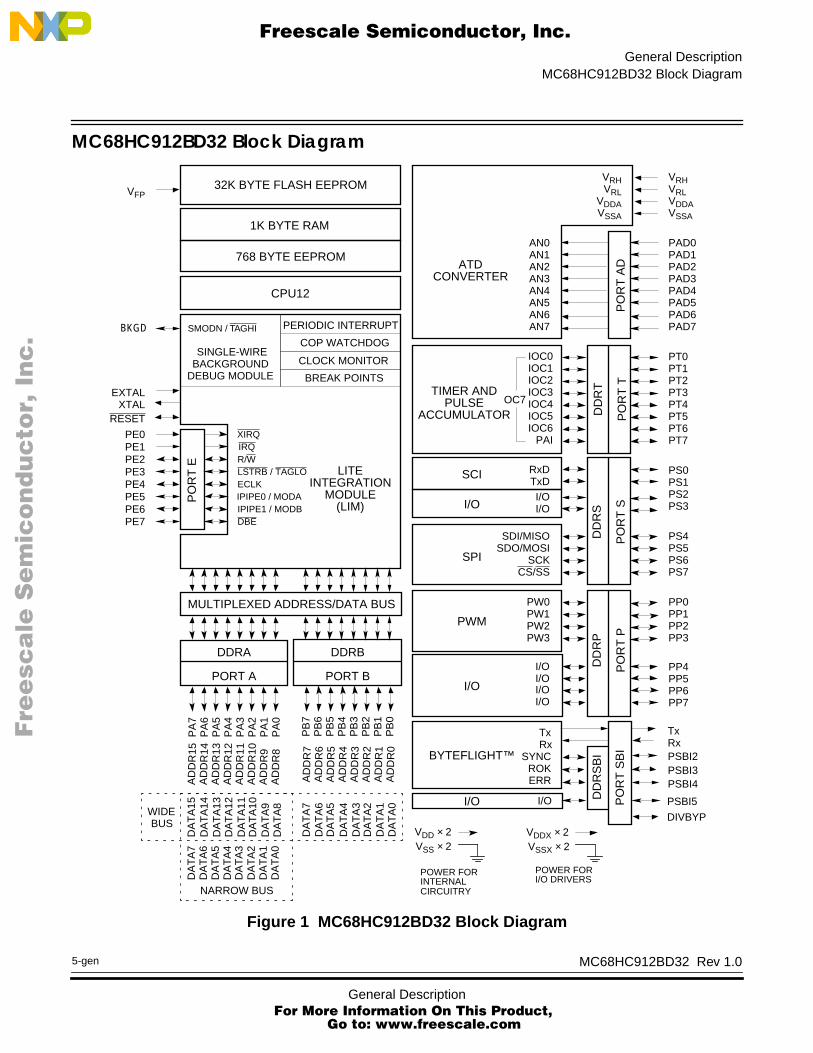
The MC68HC912BD32 microcontroller unit (MCU) is a16-bit device composed of standard on-chip peripherals including a 16-bit central processing unit (CPU12), 32K byte flash EEPROM, 1K byte RAM, 768 byte EEPROM, an asynchronous serial communications interface (SCI), a serial peripheral interface (SPI), an 8-channel timer and 16-bit pulse accumulator, a 10-bit analog-to-digital converter (ADC), a four-channel pulse-width modulator (PWM), and a Byteflight™ module. System resource mapping, clock generation, interrupt control and bus interfacing are managed by the Lite integration module (LIM). The MC68HC912BD32 has full 16-bit data paths throughout, however, the multiplexed external bus can operate in an 8-bit narrow mode so single 8-bit wide memory can be interfaced for lower cost systems.
MC68HC912BD32 Rev 1.0
1-genGeneral Description For More Information On This Product,
Go to: www.freescale.com

General Description
Fre
esc
ale
Se
mic
on
du
cto
r, I
Freescale Semiconductor, Inc.n
c..
.
Features
• 16-Bit CPU12
– Upward Compatible with M68HC11 Instruction Set
– Interrupt Stacking and Programmer’s Model Identical to M68HC11
– 20-Bit ALU
– Instruction Queue
– Enhanced Indexed Addressing
– Fuzzy Logic Instructions
• Multiplexed Bus
– Single Chip or Expanded
– 16/16 Wide or 16/8 Narrow Modes
• Memory
– 32K byte Flash EEPROM with 2K byte Erase-Protected Boot Block
– 768 byte EEPROM
– 1K byte RAM with Single-Cycle Access for Aligned or Misaligned Read/Write
• 8-Channel, 10-Bit Analog-to-Digital Converter
• 8-Channel Timer
– Each Channel Fully Configurable as Either Input Capture or Output Compare
– Simple PWM Mode
– Modulo Reset of Timer Counter
• 16-Bit Pulse Accumulator
– External Event Counting
– Gated Time Accumulation
MC68HC912BD32 Rev 1.0
General Description For More Information On This Prod
Go to: www.freescale.com
2-gen
uct,

General DescriptionFeatures
Fre
esc
ale
Se
mic
on
du
cto
r, I
Freescale Semiconductor, Inc.n
c..
.
• Pulse-Width Modulator
– 8-Bit, 4-Channel or 16-Bit, 2-Channel
– Separate Control for Each Pulse Width and Duty Cycle
– Programmable Center-Aligned or Left-Aligned Outputs
• Serial Interfaces
– Asynchronous Serial Communications Interface (SCI)
– Synchronous Serial Peripheral Interface (SPI)
• Byteflight™ Module
– Modular Architecture
– Implementation of the BMW Byteflight™ protocol
– Double buffered receive storage systems
– 16 Message Buffers in total
– Programmable Message Buffer Configuration (transmit, receive, FIFO)
– Receive FIFO for bus monitoring with programmable acceptance filter
– 10 maskable interrupt sources, generating four CPU interrupt vectors
– Programmable bus master function
– Programmable wake-up function
– Low power sleep mode
– Separate clock system, synchronization to HC12 bus system
• COP Watchdog Timer, Clock Monitor, and Periodic Interrupt Timer
• Features 80-Pin QFP Package
– Up to 50 General-Purpose I/O Lines
– 4.75V–5.25V Operation at 10 MHz
• Single-Wire Background Debug™ Mode (BDM)
• On-Chip Hardware Breakpoints
MC68HC912BD32 Rev 1.0
3-genGeneral Description For More Information On This Product,
Go to: www.freescale.com
General Description
Fre
esc
ale
Se
mic
on
du
cto
r, I
Freescale Semiconductor, Inc.n
c..
.
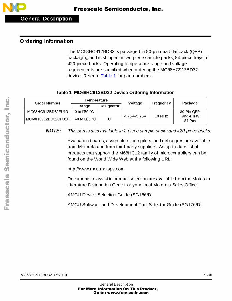
Ordering Information
The MC68HC912BD32 is packaged in 80-pin quad flat pack (QFP) packaging and is shipped in two-piece sample packs, 84-piece trays, or 420-piece bricks. Operating temperature range and voltage requirements are specified when ordering the MC68HC912BD32 device. Refer to Table 1 for part numbers.
NOTE: This part is also available in 2-piece sample packs and 420-piece bricks.
Evaluation boards, assemblers, compilers, and debuggers are available from Motorola and from third-party suppliers. An up-to-date list of products that support the M68HC12 family of microcontrollers can be found on the World Wide Web at the following URL:
http://www.mcu.motsps.com
Documents to assist in product selection are available from the Motorola Literature Distribution Center or your local Motorola Sales Office:
AMCU Device Selection Guide (SG166/D)
AMCU Software and Development Tool Selector Guide (SG176/D)
Table 1 MC68HC912BD32 Device Ordering Information
Order NumberTemperature
Voltage Frequency PackageRange Designator
MC68HC912BD32FU10 0 to +70 °C4.75V–5.25V 10 MHz
80-Pin QFPSingle Tray
84 PcsMC68HC912BD32CFU10 −40 to +85 °C C
MC68HC912BD32 Rev 1.0
General Description For More Information On This Prod
Go to: www.freescale.com
4-gen
uct,
General DescriptionMC68HC912BD32 Block Diagram
Fre
esc
ale
Se
mic
on
du
cto
r, I
Freescale Semiconductor, Inc.n
c..
.
MC68HC912BD32 Block Diagram
Figure 1 MC68HC912BD32 Block Diagram
IOC0IOC1IOC2IOC3IOC4IOC5IOC6
PAI
OC7
DD
RT
PO
RT
T
PERIODIC INTERRUPT
COP WATCHDOG
32K BYTE FLASH EEPROM
1K BYTE RAM
PO
RT
E
TIMER AND
PT0PT1PT2PT3PT4PT5PT6PT7
SPI
DD
RS
PO
RT
S
ATD
PO
RT
AD
PE1PE2
PE4PE5PE6
PE3
PAD3PAD4PAD5PAD6PAD7
V
DDA
V
SSA
V
RH
V
RL
PAD0PAD1PAD2
DDRA
PORT A
DDRB
PORT B
P
A4
PA
3P
A2
PA
1P
A0
PA
7P
A6
PA
5
PB
4P
B3
PB
2P
B1
PB
0
PB
7P
B6
PB
5
DA
TA
15
MULTIPLEXED ADDRESS/DATA BUS
RESET
EXTALXTAL
PW0PW1PW2PW3
PWM
DD
RP
PO
RT
P
PP0PP1PP2PP3
V
DD
×
2V
SS
×
2
SCI
RxDTxDI/OI/O
SDI/MISOSDO/MOSI
SCKCS/SS
PS0PS1PS2PS3
PS4PS5PS6PS7
768 BYTE EEPROM
CLOCK MONITOR
PE0
PE7
AN3AN4AN5AN6AN7
V
DDA
V
SSA
V
RH
V
RL
AN0AN1AN2
SINGLE-WIREBACKGROUND
DEBUG MODULE
SMODN / TAGHI
ECLK
R/WLSTRB / TAGLO
IPIPE0 / MODAIPIPE1 / MODB
XIRQ
DBE
PULSEACCUMULATOR
LITE
IRQ
PP4PP5PP6PP7
I/OI/OI/OI/O
I/O
I/O
RxTx
ROK
BYTEFLIGHT™
DD
RS
BI
PO
RT
SB
I
PSBI4
PSBI5
DIVBYP
ERR
I/O
I/O
TxRxPSBI2PSBI3
INTEGRATIONMODULE
(LIM)
V
FP
BREAK POINTS
CPU12
AD
DR
15A
DD
R14
AD
DR
13A
DD
R12
AD
DR
11A
DD
R10
AD
DR
9A
DD
R8
DA
TA
14D
AT
A13
DA
TA
12D
AT
A11
DA
TA
10D
AT
A9
DA
TA
8
AD
DR
7A
DD
R6
AD
DR
5A
DD
R4
AD
DR
3A
DD
R2
AD
DR
1A
DD
R0
DA
TA
7D
AT
A6
DA
TA
5D
AT
A4
DA
TA
3D
AT
A2
DA
TA
1D
AT
A0
SYNC
CONVERTER
V
SSX
×
2V
DDX
×
2
POWER FORPOWER FORI/O DRIVERSINTERNAL
CIRCUITRY
DA
TA
7D
AT
A6
DA
TA
5D
AT
A4
DA
TA
3D
AT
A2
DA
TA
1D
AT
A0
NARROW BUS
WIDEBUS
BKGD
MC68HC912BD32 Rev 1.0
5-genGeneral Description For More Information On This Product,
Go to: www.freescale.com

General Description
F
ree
sca
le S
em
ico
nd
uc
tor,
I
Freescale Semiconductor, Inc.n
c..
.
MC68HC912BD32 Rev 1.0
General Description For More Information On This Prod
Go to: www.freescale.com
6-gen
uct,

F
ree
sca
le S
em
ico
nd
uc
tor,
IFreescale Semiconductor, Inc.
nc
...
Central Processing UnitCentral Processing Unit
Contents
Introduction . . . . . . . . . . . . . . . . . . . . . . . . . . . . . . . . . . . . . . . . . . . . . 11Programming Model . . . . . . . . . . . . . . . . . . . . . . . . . . . . . . . . . . . . . . 11Data Types . . . . . . . . . . . . . . . . . . . . . . . . . . . . . . . . . . . . . . . . . . . . . 13Addressing Modes . . . . . . . . . . . . . . . . . . . . . . . . . . . . . . . . . . . . . . . 13Indexed Addressing Modes. . . . . . . . . . . . . . . . . . . . . . . . . . . . . . . . . 15Opcodes and Operands . . . . . . . . . . . . . . . . . . . . . . . . . . . . . . . . . . . 16
Introduction
The CPU12 is a high-speed, 16-bit processing unit. It has full 16-bit data paths and wider internal registers (up to 20 bits) for high-speed extended math instructions. The instruction set is a proper superset of the M68HC11instruction set. The CPU12 allows instructions with odd byte counts, including many single-byte instructions. This provides efficient use of ROM space. An instruction queue buffers program information so the CPU always has immediate access to at least three bytes of machine code at the start of every instruction. The CPU12 also offers an extensive set of indexed addressing capabilities.
Programming Model
CPU12 registers are an integral part of the CPU and are not addressed as if they were memory locations.
MC68HC912BD32 Rev 1.0
1-cpuCentral Processing Unit For More Information On This Product,
Go to: www.freescale.com

Central Processing Unit
F
ree
sca
le S
em
ico
nd
uc
tor,
I
Freescale Semiconductor, Inc.n
c..
.
Figure 2 Programming Model
Accumulators
A and B are general-purpose 8-bit accumulators used to hold operands and results of arithmetic calculations or data manipulations. Some instructions treat the combination of these two 8-bit accumulators as a 16-bit double accumulator (accumulator D).
Index registers
X and Y are used for indexed addressing mode. In the indexed addressing mode, the contents of a 16-bit index register are added to 5-bit, 9-bit, or 16-bit constants or the content of an accumulator to form the effective address of the operand to be used in the instruction.
Stack pointer
(SP) points to the last stack location used. The CPU12 supports an automatic program stack that is used to save system context during subroutine calls and interrupts, and can also be used for temporary storage of data. The stack pointer can also be used in all indexed addressing modes.
Program counter
is a 16-bit register that holds the address of the next instruction to be executed. The program counter can be used in all indexed addressing modes except autoincrement/decrement.
7
15
15
15
15
15
D
IX
IY
SP
PC
A B
NS X H I Z V C
0
0
0
0
0
0
70
CONDITION CODE REGISTER
8-BIT ACCUMULATORS A & B
16-BIT DOUBLE ACCUMULATOR D
INDEX REGISTER X
INDEX REGISTER Y
STACK POINTER
PROGRAM COUNTER
OR
MC68HC912BD32 Rev 1.0
Central Processing Unit For More Information On This Prod
Go to: www.freescale.com
2-cpu
uct,

Central Processing UnitData Types
F
ree
sca
le S
em
ico
nd
uc
tor,
I
Freescale Semiconductor, Inc.n
c..
.
Condition Code Register
(CCR) contains five status indicators, two interrupt masking bits, and a STOP disable bit. The five flags are half carry (H), negative (N), zero (Z), overflow (V), and carry/borrow (C). The half-carry flag is used only for BCD arithmetic operations. The N, Z, V, and C status bits allow for branching based on the results of a previous operation.
After a reset, the CPU fetches a vector from the appropriate address and begins executing instructions. The X and I interrupt mask bits are set to mask any interrupt requests. The S bit is also set to inhibit the STOP instruction.
Data Types
The CPU12 supports the following data types:
• Bit data
• 8-bit and 16-bit signed and unsigned integers
• 16-bit unsigned fractions
• 16-bit addresses
A byte is eight bits wide and can be accessed at any byte location. A word is composed of two consecutive bytes with the most significant byte at the lower value address. There are no special requirements for alignment of instructions or operands.
Addressing Modes
Addressing modes determine how the CPU accesses memory locations to be operated upon. The CPU12 includes all of the addressing modes of the M68HC11 CPU as well as several new forms of indexed addressing. Table 2 is a summary of the available addressing modes.
MC68HC912BD32 Rev 1.0
3-cpuCentral Processing Unit For More Information On This Product,
Go to: www.freescale.com

Central Processing Unit
F
ree
sca
le S
em
ico
nd
uc
tor,
I
Freescale Semiconductor, Inc.n
c..
.
Table 2 M68HC12 Addressing Mode Summary
Addressing Mode Source Format Abbreviation Description
Inherent
INST
(no externally supplied operands)
INH Operands (if any) are in CPU registers
Immediate
INST #
opr8i
or
INST #
opr16i
IMMOperand is included in instruction stream
8- or 16-bit size implied by context
Direct
INST
opr8a
DIROperand is the lower 8-bits of an address in
the range $0000 – $00FF
Extended
INST
opr16a
EXT Operand is a 16-bit address
Relative
INST
rel8
or
INST
rel16
RELAn 8-bit or 16-bit relative offset from the current pc is supplied in the instruction
Indexed(5-bit offset)
INST
oprx5
,
xysp
IDX5-bit signed constant offset from x, y, sp, or
pc
Indexed(auto pre-decrement)
INST
oprx3
,
–
xys
IDX Auto pre-decrement x, y, or sp by 1 ~ 8
Indexed(auto pre-increment)
INST
oprx3
,+
xys
IDX Auto pre-increment x, y, or sp by 1 ~ 8
Indexed(auto post-decrement)
INST
oprx3
,
xys
–
IDX Auto post-decrement x, y, or sp by 1 ~ 8
Indexed(auto post-increment)
INST
oprx3
,
xys
+
IDX Auto post-increment x, y, or sp by 1 ~ 8
Indexed(accumulator offset)
INST
abd
,
xysp
IDXIndexed with 8-bit (A or B) or 16-bit (D) accumulator offset from x, y, sp, or pc
Indexed(9-bit offset)
INST
oprx9
,xysp IDX19-bit signed constant offset from x, y, sp, or
pc (lower 8-bits of offset in one extension byte)
Indexed(16-bit offset)
INST oprx16,xysp IDX216-bit constant offset from x, y, sp, or pc
(16-bit offset in two extension bytes)
Indexed-Indirect(16-bit offset)
INST [oprx16,xysp] [IDX2]Pointer to operand is found at...
16-bit constant offset from x, y, sp, or pc(16-bit offset in two extension bytes)
Indexed-Indirect(D accumulator offset)
INST [D,xysp] [D,IDX]Pointer to operand is found at...x, y, sp, or pc plus the value in D
MC68HC912BD32 Rev 1.0
Central Processing Unit For More Information On This Prod
Go to: www.freescale.com
4-cpu
uct,

Central Processing UnitIndexed Addressing Modes
F
ree
sca
le S
em
ico
nd
uc
tor,
I
Freescale Semiconductor, Inc.n
c..
.
Indexed Addressing Modes
The CPU12 indexed modes reduce execution time and eliminate code size penalties for using the Y index register. CPU12 indexed addressing uses a postbyte plus zero, one, or two extension bytes after the instruction opcode. The postbyte and extensions do the following tasks:
• Specify which index register is used.
• Determine whether a value in an accumulator is used as an offset.
• Enable automatic pre- or post-increment or decrement
• Specify use of 5-bit, 9-bit, or 16-bit signed offsets.
Table 3 Summary of Indexed Operations
PostbyteCode (xb)
Source Code
SyntaxComments
rr0nnnnn,rn,r–n,r
5-bit constant offset n = –16 to +15rr can specify X, Y, SP, or PC
111rr0zsn,r–n,r
Constant offset (9- or 16-bit signed)z-0 = 9-bit with sign in LSB of postbyte(s)
1 = 16-bitif z = s = 1, 16-bit offset indexed-indirect (see below)rr can specify X, Y, SP, or PC
111rr011 [n,r]16-bit offset indexed-indirectrr can specify X, Y, SP, or PC
rr1pnnnnn,–r n,+rn,r– n,r+
Auto pre-decrement/increment or Auto post-decrement/increment ; p = pre-(0) or post-(1), n = –8 to –1, +1 to +8rr can specify X, Y, or SP (PC not a valid choice)
111rr1aaA,rB,rD,r
Accumulator offset (unsigned 8-bit or 16-bit)aa-00 = A
01 = B10 = D (16-bit)11 = see accumulator D offset indexed-indirect
rr can specify X, Y, SP, or PC
111rr111 [D,r]Accumulator D offset indexed-indirectrr can specify X, Y, SP, or PC
MC68HC912BD32 Rev 1.0
5-cpuCentral Processing Unit For More Information On This Product,
Go to: www.freescale.com

Central Processing Unit
F
ree
sca
le S
em
ico
nd
uc
tor,
I
Freescale Semiconductor, Inc.n
c..
.
Opcodes and Operands
The CPU12 uses 8-bit opcodes. Each opcode identifies a particular instruction and associated addressing mode to the CPU. Several opcodes are required to provide each instruction with a range of addressing capabilities.
Only 256 opcodes would be available if the range of values were restricted to the number that can be represented by 8-bit binary numbers. To expand the number of opcodes, a second page is added to the opcode map. Opcodes on the second page are preceded by an additional byte with the value $18.
To provide additional addressing flexibility, opcodes can also be followed by a postbyte or extension bytes. Postbytes implement certain forms of indexed addressing, transfers, exchanges, and loop primitives. Extension bytes contain additional program information such as addresses, offsets, and immediate data.
MC68HC912BD32 Rev 1.0
Central Processing Unit For More Information On This Prod
Go to: www.freescale.com
6-cpu
uct,

F
ree
sca
le S
em
ico
nd
uc
tor,
IFreescale Semiconductor, Inc.
nc
...
Pinout and Signal DescriptionsPinout and Signal Descriptions
Contents
MC68HC912BD32 Rev 1.0 Pin Assignments . . . . . . . . . . . . . . . . . . . 17Power Supply Pins . . . . . . . . . . . . . . . . . . . . . . . . . . . . . . . . . . . . . . . 19Signal Descriptions . . . . . . . . . . . . . . . . . . . . . . . . . . . . . . . . . . . . . . . 20Port Signals. . . . . . . . . . . . . . . . . . . . . . . . . . . . . . . . . . . . . . . . . . . . . 26Port Pull-Up, Pull-Down and Reduced Drive. . . . . . . . . . . . . . . . . . . . 31
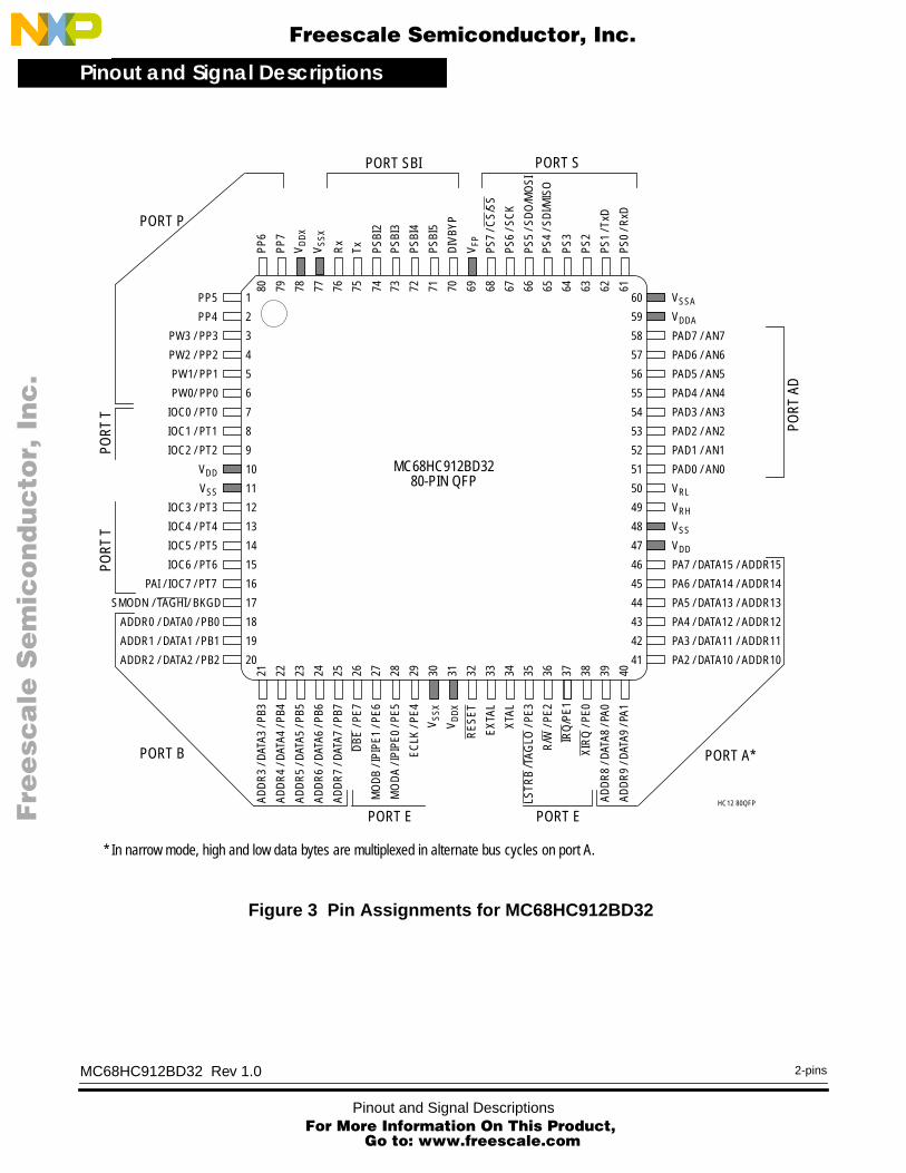
MC68HC912BD32 Rev 1.0 Pin Assignments
The MC68HC912BD32 is available in a 80-pin quad flat pack (QFP). Most pins perform two or more functions, as described in the Signal Descriptions. Figure 3 shows pin assignments. Shaded pins are power and ground.
MC68HC912BD32 Rev 1.0
1-pinsPinout and Signal Descriptions For More Information On This Product,
Go to: www.freescale.com
Pinout and Signal Descriptions
F
ree
sca
le S
em
ico
nd
uc
tor,
I
Freescale Semiconductor, Inc.n
c..
.
Figure 3 Pin Assignments for MC68HC912BD32
MC68HC912BD3280-PIN QFP
HC12 80QFP
PP5
PP4
PW3 / PP3
PW2 / PP2
PW1/ PP1
41
1
2
3
4
5
6
7
8
9
10
11
12
13
14
15
16
17
18
19
20
4021 22 23 24 25 26 27 28 29 30 31 32 33 34 35 36 37 38 39
42
43
44
45
46
47
48
49
50
51
52
53
54
55
56
57
58
59
60
6162636465666768697071727374757677787980
PA2 / DATA10 / ADDR10
PA3 / DATA11 / ADDR11
PA4 / DATA12 / ADDR12
PA5 / DATA13 / ADDR13
PA6 / DATA14 / ADDR14
PA7 / DATA15 / ADDR15
PP6
PP7
ADDR0 / DATA0 / PB0
ADDR1 / DATA1 / PB1
ADDR2 / DATA2 / PB2
SMODN / TAGHI/ BKGD
PAI / IOC7 / PT7
IOC6 / PT6
IOC5 / PT5
IOC4 / PT4
IOC3 / PT3
IOC2 / PT2
IOC1 / PT1
IOC0 / PT0
ADD
R9
/ DAT
A9 /
PA1
XIR
Q /
PE0
IRQ
/PE1
R/W
/ PE
2
LSTR
B / T
AGLO
/ PE
3
XTAL
EX
TAL
RE
SE
T
VD
DX
VS
SX
ECLK
/ PE
4
MO
DA
/ IPI
PE0
/ PE5
MO
DB
/ IPI
PE1
/ PE6
DB
E /
PE7
ADD
R7
/ DAT
A7 /
PB7
ADD
R6
/ DAT
A6 /
PB6
ADD
R5
/ DAT
A5 /
PB5
ADD
R4
/ DAT
A4 /
PB4
ADD
R3
/ DAT
A3 /
PB3
VDD
VSS
PW0/ PP0
VSSA
VDDA
PAD7 / AN7
PAD6 / AN6
PAD5 / AN5
PAD4 / AN4
PAD3 / AN3
PAD2 / AN2
PAD1 / AN1
PAD0 / AN0
VRL
VRH
VSS
VDD
PS0
/ RxD
PS1
/ TxD
PS2
PS3
PS4
/ SD
I/MIS
O
PS5
/ SD
O/M
OSI
PS6
/ SC
K
PS7
/ CS
/SS
VFP
DIV
BYP
PSBI
5
PSBI
4
PSBI
3
PSBI
2
TxRx
VS
SX
VD
DX
ADD
R8
/ DAT
A8 /
PA0
PORT
AD
PORT A*PORT B
PORT EPORT E
PORT SBI PORT S
PORT P
PORT
TPO
RT T
* In narrow mode, high and low data bytes are multiplexed in alternate bus cycles on port A.
MC68HC912BD32 Rev 1.0
Pinout and Signal Descriptions For More Information On This Prod
Go to: www.freescale.com
2-pins
uct,

Pinout and Signal DescriptionsPower Supply Pins
F
ree
sca
le S
em
ico
nd
uc
tor,
I
Freescale Semiconductor, Inc.n
c..
.
Power Supply Pins
MC68HC912BD32 power and ground pins are described below and summarized in Table 4.
Internal Power (VDD) and Ground (VSS)
Power is supplied to the MCU through VDD and VSS. Because fast signal transitions place high, short-duration current demands on the power supply, use bypass capacitors with high-frequency characteristics and place them as close to the MCU as possible. Bypass requirements depend on how heavily the MCU pins are loaded.
External Power (VDDX) and Ground (VSSX)
External power and ground for I/O drivers. Because fast signal transitions place high, short-duration current demands on the power supply, use bypass capacitors with high-frequency characteristics and place them as close to the MCU as possible. Bypass requirements depend on how heavily the MCU pins are loaded.
VDDA, VSSA Provides operating voltage and ground for the analog-to-digital converter. This allows the supply voltage to the A/D to be bypassed independently.
Analog to Digital Reference Voltages (VRH, VRL)
VFP Flash EEPROM programming voltage and supply voltage during normal operation.
MC68HC912BD32 Rev 1.0
3-pinsPinout and Signal Descriptions For More Information On This Product,
Go to: www.freescale.com

Pinout and Signal Descriptions
F
ree
sca
le S
em
ico
nd
uc
tor,
I
Freescale Semiconductor, Inc.n
c..
.
Signal Descriptions
Crystal Driver and External Clock Input (XTAL, EXTAL)
These pins provide the interface for either a crystal or a CMOS compatible clock to control the internal clock generator circuitry. Out of reset the frequency applied to EXTAL is four times the desired E–clock rate (in normal operation with DIVBYP=0; refer to Clock Divider Bypass (DIVBYP)) All the device clocks are derived from the EXTAL input frequency.
Figure 4 Common Crystal Connections
Table 4 MC68HC912BD32 Power and Ground Connection Summary
Mnemonic Pin Number Description
VDD 10, 47Internal power and ground.
VSS 11, 48
VDDX 31, 78External power and ground, supply to pin drivers.
VSSX 30, 77
VDDA 59 Operating voltage and ground for the analog-to-digital converter, allows the supply voltage to the A/D to be bypassed independently.VSSA 60
VRH 49Reference voltages for the analog-to-digital converter.
VRL 50
VFP 69Programming voltage for the Flash EEPROM and required supply for normal operation.
10 MΩMCU
C
C
EXTAL
XTAL
4 x E (DIVBYP=0)
CRYSTAL2 x E (DIVBYP=1)
MC68HC912BD32 Rev 1.0
Pinout and Signal Descriptions For More Information On This Prod
Go to: www.freescale.com
4-pins
uct,

Pinout and Signal DescriptionsSignal Descriptions
F
ree
sca
le S
em
ico
nd
uc
tor,
I
Freescale Semiconductor, Inc.n
c..
.
Figure 5 External Oscillator Connections
XTAL is the crystal output.The XTAL pin must be left unterminated when an external CMOS compatible clock input is connected to the EXTAL pin. The XTAL output is normally intended to drive only a crystal. The XTAL output can be buffered with a high-impedance buffer to drive the EXTAL input of another device.
In all cases take extra care in the circuit board layout around the oscillator pins. Load capacitances shown in the oscillator circuits include all stray layout capacitances. Refer to Figure 4 and Figure 5 for diagrams of oscillator circuits.
E-Clock Output (ECLK)
ECLK is the output connection for the internal bus clock and is used to demultiplex the address and data and is used as a timing reference. ECLK frequency is equal to 1/4 the crystal frequency out of reset (in normal operation with DIVBYP=0, refer to Clock Divider Bypass (DIVBYP)).
In normal single-chip mode the E-clock output is off at reset to reduce the effects of RFI, but can be turned on if necessary.
In special single-chip mode the E-clock output is on at reset but can be turned off.
In special peripheral mode the E clock is an input to the MCU.
All clocks, including the E clock, are halted when the MCU is in STOP mode. It is possible to configure the MCU to interface to slow external memory. ECLK can be stretched for such accesses.
NC
MCU
EXTAL
XTAL
4 x E (DIVBYP=0)
CMOS-COMPATIBLEEXTERNAL OSCILLATOR
2 x E (DIVBYP=1)
MC68HC912BD32 Rev 1.0
5-pinsPinout and Signal Descriptions For More Information On This Product,
Go to: www.freescale.com

Pinout and Signal Descriptions
F
ree
sca
le S
em
ico
nd
uc
tor,
I
Freescale Semiconductor, Inc.n
c..
.
Reset (RESET) An active low bidirectional control signal, RESET, acts as an input to initialize the MCU to a known start-up state. It also acts as an open-drain output to indicate that an internal failure has been detected in either the clock monitor or COP watchdog circuit. The MCU goes into reset asynchronously and comes out of reset synchronously. This allows the part to reach a proper reset state even if the clocks have failed, while allowing synchronized operation when starting out of reset.
It is possible to determine whether a reset was caused by an internal source or an external source. An internal source drives the pin low for 16 cycles; eight cycles later the pin is sampled. If the pin has returned high, either the COP watchdog vector or clock monitor vector will be taken. If the pin is still low, the external reset is determined to be active and the reset vector is taken. Hold reset low for at least 32 cycles to assure that the reset vector is taken in the event that an internal COP watchdog time-out or clock monitor fail occurs.
Maskable Interrupt Request (IRQ)
The IRQ input provides a means of applying asynchronous interrupt requests to the MCU. Either falling edge-sensitive triggering or level-sensitive triggering is program selectable (INTCR register). IRQ is always configured to level-sensitive triggering at reset. When the MCU is reset the IRQ function is masked in the condition code register.
This pin is always an input and can always be read. There is an active pull-up on this pin while in reset and immediately out of reset. The pullup can be turned off by clearing PUPE in the PUCR register.
Nonmaskable Interrupt (XIRQ)
The XIRQ input provides a means of requesting a nonmaskable interrupt after reset initialization. During reset, the X bit in the condition code register (CCR) is set and any interrupt is masked until MCU software enables it. Because the XIRQ input is level sensitive, it can be connected to a multiple-source wired-OR network. This pin is always an input and can always be read. There is an active pull-up on this pin while in reset and immediately out of reset. The pullup can be turned off by clearing PUPE in the PUCR register. XIRQ is often used as a power loss detect interrupt.
MC68HC912BD32 Rev 1.0
Pinout and Signal Descriptions For More Information On This Prod
Go to: www.freescale.com
6-pins
uct,
Pinout and Signal DescriptionsSignal Descriptions
MC68HC912BD32 Rev 1.0
F
ree
sca
le S
em
ico
nd
uc
tor,
I
Freescale Semiconductor, Inc.n
c..
.
7-pins
Whenever XIRQ or IRQ are used with multiple interrupt sources (IRQ must be configured for level-sensitive operation if there is more than one source of IRQ interrupt), each source must drive the interrupt input with an open-drain type of driver to avoid contention between outputs. There must also be an interlock mechanism at each interrupt source so that the source holds the interrupt line low until the MCU recognizes and acknowledges the interrupt request. If the interrupt line is held low, the MCU will recognize another interrupt as soon as the interrupt mask bit in the MCU is cleared (normally upon return from an interrupt).
Mode Select (SMODN, MODA, and MODB)
The state of these pins during reset determine the MCU operating mode. After reset, MODA and MODB can be configured as instruction queue tracking signals IPIPE0 and IPIPE1. MODA and MODB have active pulldowns during reset.
The SMODN pin can be used as BKGD or TAGHI after reset.
Single-Wire Background Mode Pin (BKGD)
The BKGD pin receives and transmits serial background debugging commands. A special self-timing protocol is used. The BKGD pin has an active pullup when configured as input; BKGD has no pullup control. Refer to Development Support.
External Address and Data Buses (ADDR[15:0] and DATA[15:0])
External bus pins share function with general-purpose I/O ports A and B. In single-chip operating modes, the pins can be used for I/O; in expanded modes, the pins are used for the external buses.
In expanded wide mode, ports A and B are used for multiplexed 16-bit data and address buses. PA[7:0] correspond to ADDR[15:8]/DATA[15:8]; PB[7:0] correspond to ADDR[7:0]/DATA[7:0].
In expanded narrow mode, ports A and B are used for the16-bit address bus, and an 8-bit data bus is multiplexed with the most significant half of the address bus on port A. In this mode, 16-bit data is handled as two back-to-back bus cycles, one for the high byte followed by one for the low byte. PA[7:0] correspond to ADDR[15:8] and to DATA[15:8] or DATA[7:0], depending on the bus cycle. The state of the address pin
Pinout and Signal Descriptions For More Information On This Product,
Go to: www.freescale.com
Pinout and Signal Descriptions
F
ree
sca
le S
em
ico
nd
uc
tor,
I
Freescale Semiconductor, Inc.n
c..
.
should be latched at the rising edge of E. To allow for maximum address setup time at external devices, a transparent latch should be used.
Read/Write (R/W) In all modes this pin can be used as I/O and is a general-purpose input with an active pull-up out of reset. If the read/write function is required it should be enabled by setting the RDWE bit in the PEAR register. External writes will not be possible until enabled.
Low-Byte Strobe (LSTRB)
In all modes this pin can be used as I/O and is a general-purpose input with an active pull-up out of reset. If the strobe function is required, it should be enabled by setting the LSTRE bit in the PEAR register. This signal is used in write operations and so external low byte writes will not be possible until this function is enabled. This pin is also used as TAGLO in Special Expanded modes and is multiplexed with the LSTRB function.
Instruction Queue Tracking Signals (IPIPE1 and IPIPE0)
These signals are used to track the state of the internal instruction execution queue. Execution state is time-multiplexed on the two signals. Refer to Development Support.
Data Bus Enable (DBE)
The DBE pin (PE7) is an active low signal that will be asserted low during E-clock high time. DBE provides separation between output of a multiplexed address and the input of data. When an external address is stretched, DBE is asserted during what would be the last quarter cycle of the last E-clock cycle of stretch. In expanded modes this pin is used to enable the drive control of external buses during external reads. Use of the DBE is controlled by the NDBE bit in the PEAR register. DBE is enabled out of reset in expanded modes. This pin has an active pullup during and after reset in single chip modes.
Clock Divider Bypass (DIVBYP)
This feature is intended for test purposes only. The DIVBYP pin is input only. The logic state of this static signal is active high. There is an active pull-down on this pin to disable the clock divider bypass when left open. For application it is recommended to tie DIVBYP to VSS. The E-clock rate is 1/4 of the frequency applied to EXTAL.
MC68HC912BD32 Rev 1.0
Pinout and Signal Descriptions For More Information On This Prod
Go to: www.freescale.com
8-pins
uct,

Pinout and Signal DescriptionsSignal Descriptions
MC68HC912BD32 Rev 1.0
F
ree
sca
le S
em
ico
nd
uc
tor,
I
Freescale Semiconductor, Inc.n
c..
.
9-pins
For test the clock divider bypass is activated by setting DIVBYP to 1. The E-clock rate is 1/2 of the frequency applied to EXTAL.
Table 5 MC68HC912BD32 Signal Description Summary
Pin Name Pin Number Description
PW[3:0] 3–6 Pulse Width Modulator channel outputs.
ADDR[7:0]DATA[7:0]
25–18 External bus pins share function with general-purpose I/O ports A and B. In single chip modes, the pins can be used for I/O. In expanded modes, the pins are used for the external buses.ADDR[15:8]
DATA[15:8]46–39
IOC[7:0] 16–12, 9–7 Pins used for input capture and output compare in the timer and pulse accumulator subsystem.
PAI 16 Pulse accumulator input
AN[7:0] 58–51 Analog inputs for the analog-to-digital conversion module
DBE 26Data bus control and, in expanded mode, enables the drive control of external buses during external reads.
MODB, MODA 27, 28 State of mode select pins during reset determine the initial operating mode of the MCU. After reset, MODB and MODA can be configured as instruction queue tracking signals IPIPE1 and IPIPE0 or as general-purpose I/O pins.IPIPE1, IPIPE0 27, 28
ECLK 29E Clock is the output connection for the external bus clock. ECLK is used as a timing reference and for address demultiplexing.
RESET 32An active low bidirectional control signal, RESET acts as an input to initialize the MCU to a known start-up state, and an output when COP or clock monitor causes a reset.
EXTAL 33 Crystal driver and external clock input pins. On reset all the device clocks are derived from the EXTAL input frequency. XTAL is the crystal output.XTAL 34
LSTRB 35Low byte strobe (0 = low byte valid), in all modes this pin can be used as I/O. The low strobe function is the exclusive-NOR of A0 and the internal SZ8 signal. (The SZ8 internal signal indicates the size 16/8 access.)
TAGLO 35 Pin used in instruction tagging. See Development Support.
R/W 36Indicates direction of data on expansion bus. Shares function with general-purpose I/O. Read/write in expanded modes.
IRQ 37Maskable interrupt request input provides a means of applying asynchronous interrupt requests to the MCU. Either falling edge-sensitive triggering or level-sensitive triggering is program selectable (INTCR register).
XIRQ 38Provides a means of requesting asynchronous nonmaskable interrupt requests after reset initialization
BKGD 17Single-wire background interface pin is dedicated to the background debug function. During reset, this pin determines special or normal operating mode.
TAGHI 17 Pin used in instruction tagging. See Development Support.
Rx 76 Byteflight™ receive pin
Tx 75 Byteflight™ transmit pin
Pinout and Signal Descriptions For More Information On This Product,
Go to: www.freescale.com

Pinout and Signal Descriptions
F
ree
sca
le S
em
ico
nd
uc
tor,
I
Freescale Semiconductor, Inc.n
c..
.
Port Signals
The MC68HC912BD32 incorporates eight ports which are used to control and access the various device subsystems. When not used for these purposes, port pins may be used for general-purpose I/O. In addition to the pins described below, each port consists of a data register which can be read and written at any time, and, with the exception of port AD, PE[1:0] and port SBI[1:0], a data direction register which controls the direction of each pin. After reset all port pins are configured as input.
Port A Port A pins are used for address and data in expanded modes. The port data register is not in the address map during expanded and peripheral mode operation. When it is in the map, port A can be read or written at anytime.
Register DDRA determines whether each port A pin is an input or output. DDRA is not in the address map during expanded and peripheral mode operation. Setting a bit in DDRA makes the corresponding bit in port A an output; clearing a bit in DDRA makes the corresponding bit in port A an input. The default reset state of DDRA is all zeroes.
When the PUPA bit in the PUCR register is set, all port A input pins are pulled-up internally by an active pull-up device. This bit has no effect if the port is being used in expanded modes as the pull-ups are inactive.
Setting the RDPA bit in register RDRIV causes all port A outputs to have reduced drive level. RDRIV can be written once after reset. RDRIV is not
CS/SS 68 Slave select output for SPI master mode, input for slave mode or master mode.
SCK 67 Serial clock for SPI system.
SDO/MOSI 66 Master out/slave in pin for serial peripheral interface
SDI/MISO 65 Master in/slave out pin for serial peripheral interface
TxD 62 SCI transmit pin
RxD 61 SCI receive pin
DIVBYP 70 Clock divider bypass
Table 5 MC68HC912BD32 Signal Description Summary
Pin Name Pin Number Description
MC68HC912BD32 Rev 1.0
Pinout and Signal Descriptions For More Information On This Prod
Go to: www.freescale.com
10-pins
uct,

Pinout and Signal DescriptionsPort Signals
MC68HC912BD32 Rev 1.0
F
ree
sca
le S
em
ico
nd
uc
tor,
I
Freescale Semiconductor, Inc.n
c..
.
11-pins
in the address map in peripheral mode. Refer to Bus Control and Input/Output.
Port B Port B pins are used for address and data in expanded modes. The port data register is not in the address map during expanded and peripheral mode operation. When it is in the map, port B can be read or written at anytime.
Register DDRB determines whether each port B pin is an input or output. DDRB is not in the address map during expanded and peripheral mode operation. Setting a bit in DDRB makes the corresponding bit in port B an output; clearing a bit in DDRB makes the corresponding bit in port B an input. The default reset state of DDRB is all zeroes.
When the PUPB bit in the PUCR register is set, all port B input pins are pulled-up internally by an active pull-up device. This bit has no effect if the port is being used in expanded modes as the pull-ups are inactive.
Setting the RDPB bit in register RDRIV causes all port B outputs to have reduced drive level. RDRIV can be written once after reset. RDRIV is not in the address map in peripheral mode. Refer to Bus Control and Input/Output.
Port E Port E pins operate differently from port A and B pins. Port E pins are used for bus control signals and interrupt service request signals. When a pin is not used for one of these specific functions, it can be used as general-purpose I/O. However, two of the pins (PE[1:0]) can only be used for input, and the states of these pins can be read in the port data register even when they are used for IRQ and XIRQ.
The PEAR register determines pin function, and register DDRE determines whether each pin is an input or output when it is used for general-purpose I/O. PEAR settings override DDRE settings. Because PE[1:0] are input-only pins, only DDRE[7:2] have effect. Setting a bit in the DDRE register makes the corresponding bit in port E an output; clearing a bit in the DDRE register makes the corresponding bit in port E an input. The default reset state of DDRE is all zeroes.
Pinout and Signal Descriptions For More Information On This Product,
Go to: www.freescale.com

Pinout and Signal Descriptions
F
ree
sca
le S
em
ico
nd
uc
tor,
I
Freescale Semiconductor, Inc.n
c..
.
When the PUPE bit in the PUCR register is set, PE[7,3,2,1,0] are pulled up. PE[7,3,2,1,0] are pulled up active devices, while PE1 is always pulled up by means of an internal resistor.
Neither port E nor DDRE is in the map in peripheral mode; neither is in the internal map in expanded modes with EME set.
Setting the RDPE bit in register RDRIV causes all port E outputs to have reduced drive level. RDRIV can be written once after reset. RDRIV is not in the address map in peripheral mode. Refer to Bus Control and Input/Output.
Port SBI The port SBI has four general-purpose I/O pins, PSBI[5:2]. The DIVBYP pin, the Byteflight™ receive pin, Rx, and transmit pin, Tx, cannot be configured as general-purpose I/O on port SBI.
Register DDRSBI determines whether each port SBI pin PSBI[5:2] is an input or output. Setting a bit in DDRSBI makes the corresponding pin in port SBI an output; clearing a bit makes the corresponding pin an input. After reset port SBI pins PSBI[5:2] are configured as inputs.
When a read to the port SBI is performed, the values for Bit 7 and Bit 6 depend on the contents of the port SBI data register, PORTSBI[7:6] and the of contents of DDRSBI[7:6]. Refer to Table 6 for the returned values.
When the PUESBI bit in the PCTLSBI register is set, port SBI input pins PSBI[5:2] are pulled up internally by an active pull-up device.
Setting the RDRSBI bit in register PCTLSBI causes the port SBI outputs PSBI[5:2] to have reduced drive level. Levels are at normal drive capability after reset. RDRSBI can be written anytime after reset. Refer to Byteflight™ Module.
Table 6 Port SBI Read accesses
DDRSBI[Bit x]Read data values
Bit 7 Bit 6 Bit 5... Bit 2
0 0 DIVBYP PSBI[5:2]
1 PORTSBI[7] PORTSBI[6] PORTSBI[5:2]
MC68HC912BD32 Rev 1.0
Pinout and Signal Descriptions For More Information On This Prod
Go to: www.freescale.com
12-pins
uct,

Pinout and Signal DescriptionsPort Signals
MC68HC912BD32 Rev 1.0
F
ree
sca
le S
em
ico
nd
uc
tor,
I
Freescale Semiconductor, Inc.n
c..
.
13-pins
Port AD Input to the analog-to-digital subsystem and general-purpose input. When analog-to-digital functions are not enabled, the port has eight general-purpose input pins, PAD[7:0]. The ADPU bit in the ATDCTL2 register enables the A/D function.
Port AD pins are inputs; no data direction register is associated with this port. The port has no resistive input loads and no reduced drive controls. Refer to Analog to Digital Converter.
Port P The four pulse-width modulation channel outputs share general-purpose port P pins. The PWM function is enabled with the PWEN register. Enabling PWM pins takes precedence over the general-purpose port. When pulse-width modulation is not in use, the port pins may be used for general-purpose I/O.
Register DDRP determines pin direction of port P when used for general-purpose I/O. When DDRP bits are set, the corresponding pin is configured for output. On reset the DDRP bits are cleared and the corresponding pin is configured for input.
When the PUPP bit in the PWCTL register is set, all input pins are pulled up internally by an active pull-up device. Pullups are disabled after reset.
Setting the RDPP bit in the PWCTL register configures all port P outputs to have reduced drive levels. Levels are at normal drive capability after reset. The PWCTL register can be read or written anytime after reset. Refer to Pulse Width Modulator.
Port T This port provides eight general-purpose I/O pins when not enabled for input capture and output compare in the timer and pulse accumulator subsystem. The TEN bit in the TSCR register enables the timer function. The pulse accumulator subsystem is enabled with the PAEN bit in the PACTL register.
Register DDRT determines pin direction of port T when used for general-purpose I/O. When DDRT bits are set, the corresponding pin is configured for output. On reset the DDRT bits are cleared and the corresponding pin is configured for input.
Pinout and Signal Descriptions For More Information On This Product,
Go to: www.freescale.com

Pinout and Signal Descriptions
F
ree
sca
le S
em
ico
nd
uc
tor,
I
Freescale Semiconductor, Inc.n
c..
.
When the PUPT bit in the TMSK2 register is set, all input pins are pulled up internally by an active pull-up device. Pullups are disabled after reset.
Setting the RDPT bit in the TMSK2 register configures all port T outputs to have reduced drive levels. Levels are at normal drive capability after reset. The TMSK2 register can be read or written anytime after reset Refer to Standard Timer Module.
Port S Port S is the 8-bit interface to the standard serial interface consisting of the serial communications interface (SCI) and serial peripheral interface (SPI) subsystems. Port S pins are available for general-purpose parallel I/O when standard serial functions are not enabled.
Port S pins serve several functions depending on the various internal control registers. If WOMS bit in the SC0CR1register is set, the P-channel drivers of the output buffers are disabled for bits 0 through 1 (2 through 3). If SWOM bit in the SP0CR1 register is set, the P-channel drivers of the output buffers are disabled for bits 4 through 7. (wired-OR mode). The open drain control effects to both the serial and the general-purpose outputs. If the RDPSx bits in the PURDS register are set, the appropriate Port S pin drive capabilities are reduced. If PUPSx bits in the PURDS register are set, the appropriate pull-up device is connected to each port S pin which is programmed as a general-purpose input. If the pin is programmed as a general-purpose output, the pull-up is disconnected from the pin regardless of the state of the individual PUPSx bits. See Serial Interface.
Table 7 MC68HC912BD32 Port Description Summary
Port Name
PinNumbers
Data DirectionDD Register (Address) Description
Port APA[7:0]
46–39In/Out
DDRA ($0002)Port A and port B pins are used for address and data in expanded modes. The port data registers are not in the address map during expanded and peripheral mode operation. When in the map, port A and port B can be read or written any time.DDRA and DDRB are not in the address map in expanded or peripheral modes.
Port BPB[7:0]
25–18In/Out
DDRB ($0003)
Port ADPAD[7:0]
58–51 In Analog-to-digital converter and general-purpose I/O.
MC68HC912BD32 Rev 1.0
Pinout and Signal Descriptions For More Information On This Prod
Go to: www.freescale.com
14-pins
uct,

Pinout and Signal DescriptionsPort Pull-Up, Pull-Down and Reduced Drive
MC68HC912BD32 Rev 1.0
F
ree
sca
le S
em
ico
nd
uc
tor,
I
Freescale Semiconductor, Inc.n
c..
.
15-pins
Port Pull-Up, Pull-Down and Reduced Drive
MCU ports can be configured for internal pull-up. To reduce power consumption and RFI, the pin output drivers can be configured to operate at a reduced drive level. Reduced drive causes a slight increase in transition time depending on loading and should be used only for ports which have a light loading. Table 8 summarizes the port pull-up default status and controls.
Port SBIDIVBYP
PSBI[5:2]TxSBIRxSBI
70–76
In/OutDDRSBI ($0112)
for PSBI[5:2]TxSBI Out
RxSBI, DIVBYP In
Byteflight™ subsystem with Tx output, Rx and divider bypass input and general-purpose I/O on PSBI[5:2].
Port EPE[7:0]
26–29, 35–38
PE[1:0] InPE[7:2] In/OutDDRE ($0009)
Mode selection , bus control signals and interrupt service request signals; or general-purpose I/O.
Port PPP[7:0]
79, 80, 1–6In/Out
DDRP ($0057)General-purpose I/O. PP[3:0] are use with the pulse-width modulator when enabled.
Port SPS[7:0]
68–61In/Out
DDRS ($00D7)Serial communications interface and serial peripheral interface subsystems and general-purpose I/O.
Port TPT[7:0]
16–12, 9–7In/Out
DDRT ($00AF)
General-purpose I/O when not enabled for input capture and output compare in the timer and pulse accumulator subsystem.
Table 7 MC68HC912BD32 Port Description Summary
Port Name
PinNumbers
Data DirectionDD Register (Address) Description
Table 8 Port Pull-Up, Pull-Down and Reduced Drive Summary
Enable Bit Reduced Drive Control Bit
PortName
ResistiveInput Loads
Register(Address)
Bit Name
Reset State
Register(Address)
Bit Name
Reset State
Port A Pull-up PUCR ($000C) PUPA Disabled RDRIV ($000D) RDPA Full Drive
Port B Pull-up PUCR ($000C) PUPB Disabled RDRIV ($000D) RDPB Full Drive
Port E:
PE7, PE[3:0] Pull-up PUCR ($000C) PUPE Enabled RDRIV ($000D) RDPE Full Drive
PE[6:4] None — RDRIV ($000D) RDPE Full Drive
PE[6:5] Pull-down Enabled During Reset — — —
Pinout and Signal Descriptions For More Information On This Product,
Go to: www.freescale.com

Pinout and Signal Descriptions
F
ree
sca
le S
em
ico
nd
uc
tor,
I
Freescale Semiconductor, Inc.n
c..
.
Port P Pull-up PWCTL ($0054) PUPP Disabled PWCTL ($0054) RDPP Full Drive
Port S Pull-up PURDS ($00DB) PUPS0 Disabled PURDS ($00DB) RDPS0 Full Drive
PS[3:2] Pull-up PURDS ($00DB) PUPS1 Disabled PURDS ($00DB) RDPS1 Full Drive
PS[7:4] Pull-up PURDS ($00DB) PUPS2 Disabled PURDS ($00DB) RDPS2 Full Drive
Port T Pull-up TMSK2 ($008D) PUPT Disabled TMSK2 ($008D) RDPT Full Drive
Port SBI:
DIVBYP Pull-down Always enabled —
PSBI[5:2] Pull-up PCTLSBI ($0110) PUESBI Disabled PCTLSBI ($0110) RDRSBI Full Drive
TxSBI None — — — Full Drive
RxSBI Pull-up — — Enabled —
Port AD None — —
BKGD Pull-up — — Enabled — — Full Drive
Table 8 Port Pull-Up, Pull-Down and Reduced Drive Summary
Enable Bit Reduced Drive Control Bit
MC68HC912BD32 Rev 1.0
Pinout and Signal Descriptions For More Information On This Prod
Go to: www.freescale.com
16-pins
uct,

F
ree
sca
le S
em
ico
nd
uc
tor,
IFreescale Semiconductor, Inc.
nc
...
RegistersRegisters
Contents
Introduction . . . . . . . . . . . . . . . . . . . . . . . . . . . . . . . . . . . . . . . . . . . . . 33
Introduction
The register block can be mapped to any 2-Kbyte boundary within the standard 64-Kbyte address space by manipulating bits REG[15:11] in the INITRG register. INITRG establishes the upper five bits of the register block’s 16-bit address. The register block occupies the first 512 bytes of the 2-Kbyte block. Default addressing (after reset) is indicated in the table below. For additional information refer to 5 Operating Modes and Resource Mapping.
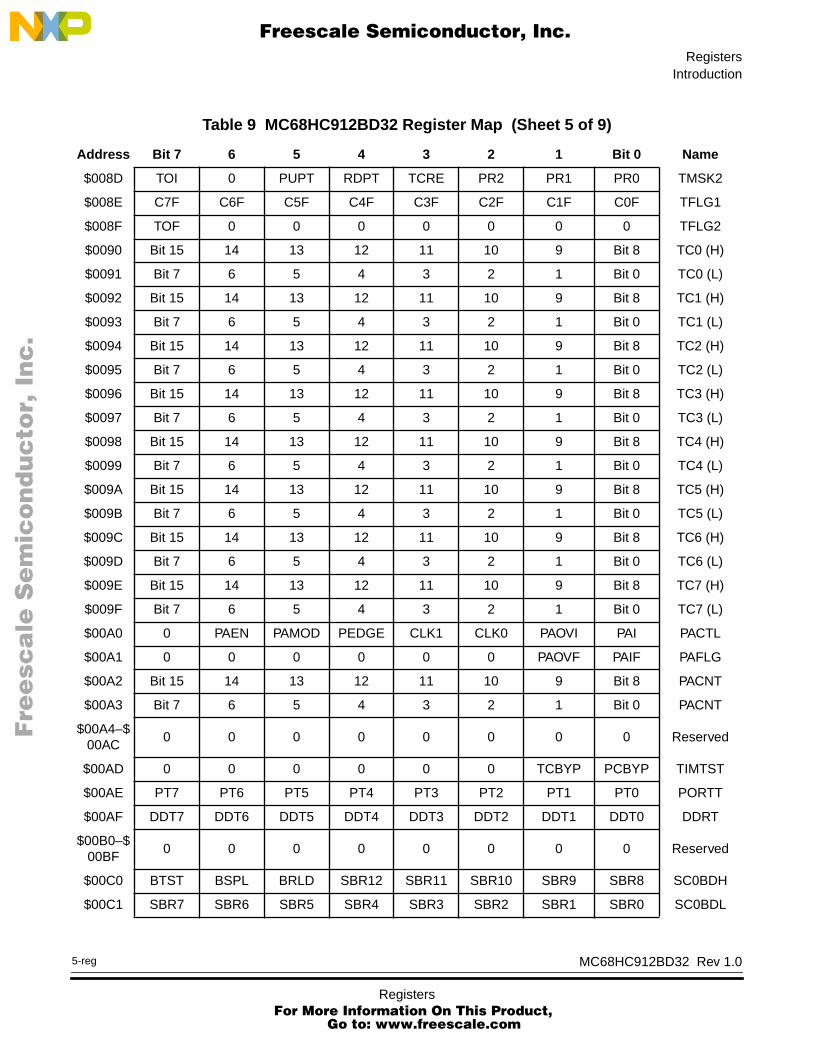
Table 9 MC68HC912BD32 Register Map (Sheet 1 of 9)
Address Bit 7 6 5 4 3 2 1 Bit 0 Name
$0000 PA7 PA6 PA5 PA4 PA3 PA2 PA1 PA0 PORTA(1)
$0001 PB7 PB6 PB5 PB4 PB3 PB2 PB1 PB0 PORTB
$0002 DDA7 DDA6 DDA5 DDA4 DDA3 DDA2 DDA1 DDA0 DDRA
$0003 DDB7 DDB6 DDB5 DDB4 DDB3 DDB2 DDB1 DDB0 DDRB
$0004 0 0 0 0 0 0 0 0 Reserved
$0005 0 0 0 0 0 0 0 0 Reserved
$0006 0 0 0 0 0 0 0 0 Reserved
$0007 0 0 0 0 0 0 0 0 Reserved
$0008 PE7 PE6 PE5 PE4 PE3 PE2 PE1 PE0 PORTE(2)
$0009 DDE7 DDE6 DDE5 DDE4 DDE3 DDE2 0 0 DDRE
$000A NDBE 0 PIPOE NECLK LSTRE RDWE 0 0 PEAR
$000B SMODN MODB MODA ESTR IVIS EBSWAI 0 EME MODE(3)
MC68HC912BD32 Rev 1.0
1-regRegisters For More Information On This Product,
Go to: www.freescale.com

Registers
F
ree
sca
le S
em
ico
nd
uc
tor,
I
Freescale Semiconductor, Inc.n
c..
.
$000C 0 0 0 PUPE 0 0 PUPB PUPA PUCR
$000D 0 0 0 0 RDPE 0 RDPB RDPA RDRIV
$000E 0 0 0 0 0 0 0 0 Reserved
$000F 0 0 0 0 0 0 0 0 Reserved
$0010 RAM15 RAM14 RAM13 RAM12 RAM11 0 0 0 INITRM
$0011 REG15 REG14 REG13 REG12 REG11 0 0 MMSWAI INITRG
$0012 EE15 EE14 EE13 EE12 0 0 0 EEON INITEE
$0013 0 NDRF RFSTR1 RFSTR0 EXSTR1 EXSTR0 MAPROM ROMON MISC
$0014 RTIE RSWAI RSBCK 0 RTBYP RTR2 RTR1 RTR0 RTICTL
$0015 RTIF 0 0 0 0 0 0 0 RTIFLG
$0016 CME FCME FCM FCOP DISR CR2 CR1 CR0 COPCTL
$0017 Bit 7 6 5 4 3 2 1 Bit 0 COPRST
$0018 ITE6 ITE8 ITEA ITEC ITEE ITF0 ITF2 ITF4 ITST0
$0019 ITD6 ITD8 ITDA ITDC ITDE ITE0 ITE2 ITE4 ITST1
$001A ITC6 ITC8 ITCA ITCC ITCE ITD0 ITD2 ITD4 ITST2
$001B 0 0 0 0 0 ITC0 ITC2 ITC4 ITST3
$001C–$001D
0 0 0 0 0 0 0 0 Reserved
$001E IRQE IRQEN DLY 0 0 0 0 0 INTCR
$001F 1 1 PSEL5 PSEL4 PSEL3 PSEL2 PSEL1 0 HPRIO
$0020 BKEN1 BKEN0 BKPM 0 BK1ALE BK0ALE 0 0 BRKCT0
$0021 0 BKDBE BKMBH BKMBL BK1RWE BK1RW BK0RWE BK0RW BRKCT1
$0022 Bit 15 14 13 12 11 10 9 Bit 8 BRKAH
$0023 Bit 7 6 5 4 3 2 1 Bit 0 BRKAL
$0024 Bit 15 14 13 12 11 10 9 Bit 8 BRKDH
$0025 Bit 7 6 5 4 3 2 1 Bit 0 BRKDL
$0026–$003F
0 0 0 0 0 0 0 0 Reserved
$0040 CON23 CON01 PCKA2 PCKA1 PCKA0 PCKB2 PCKB1 PCKB0 PWCLK
$0041 PCLK3 PCLK2 PCLK1 PCLK0 PPOL3 PPOL2 PPOL1 PPOL0 PWPOL
$0042 0 0 0 0 PWEN3 PWEN2 PWEN1 PWEN0 PWEN
$0043 0 6 5 4 3 2 1 Bit 0 PWPRES
Table 9 MC68HC912BD32 Register Map (Sheet 2 of 9)
Address Bit 7 6 5 4 3 2 1 Bit 0 Name
MC68HC912BD32 Rev 1.0
Registers For More Information On This Prod
Go to: www.freescale.com
2-reg
uct,

RegistersIntroduction
F
ree
sca
le S
em
ico
nd
uc
tor,
I
Freescale Semiconductor, Inc.n
c..
.
$0044 Bit 7 6 5 4 3 2 1 Bit 0 PWSCAL0
$0045 Bit 7 6 5 4 3 2 1 Bit 0 PWSCNT0
$0046 Bit 7 6 5 4 3 2 1 Bit 0 PWSCAL1
$0047 Bit 7 6 5 4 3 2 1 Bit 0 PWSCNT1
$0048 Bit 7 6 5 4 3 2 1 Bit 0 PWCNT0
$0049 Bit 7 6 5 4 3 2 1 Bit 0 PWCNT1
$004A Bit 7 6 5 4 3 2 1 Bit 0 PWCNT2
$004B Bit 7 6 5 4 3 2 1 Bit 0 PWCNT3
$004C Bit 7 6 5 4 3 2 1 Bit 0 PWPER0
$004D Bit 7 6 5 4 3 2 1 Bit 0 PWPER1
$004E Bit 7 6 5 4 3 2 1 Bit 0 PWPER2
$004F Bit 7 6 5 4 3 2 1 Bit 0 PWPER3
$0050 Bit 7 6 5 4 3 2 1 Bit 0 PWDTY0
$0051 Bit 7 6 5 4 3 2 1 Bit 0 PWDTY1
$0052 Bit 7 6 5 4 3 2 1 Bit 0 PWDTY2
$0053 Bit 7 6 5 4 3 2 1 Bit 0 PWDTY3
$0054 0 0 0 PSWAI CENTR RDP PUPP PSBCK PWCTL
$0055 DISCR DISCP DISCAL 0 0 0 0 0 PWTST
$0056 PP7 PP6 PP5 PP4 PP3 PP2 PP1 PP0 PORTPP
$0057 DDP7 DDP6 DDP5 DDP4 DDP3 DDP2 DDP1 DDP0 DDRP
$0058–$005F
0 0 0 0 0 0 0 0 Reserved
$0060 0 0 0 0 0 0 0 0 ATDCTL0
$0061 0 0 0 0 0 0 0 0 ATDCTL1
$0062 ADPU AFFC AWAI 0 0 0 ASCIE ASCIF ATDCTL2
$0063 0 0 0 0 0 0 FRZ1 FRZ0 ATDCTL3
$0064 S10BM SMP1 SMP0 PRS4 PRS3 PRS2 PRS1 PRS0 ATDCTL4
$0065 0 S8CM SCAN MULT CD CC CB CA ATDCTL5
$0066 SCF 0 0 0 0 CC2 CC1 CC0 ATDSTAT
$0067 CCF7 CCF6 CCF5 CCF4 CCF3 CCF2 CCF1 CCF0 ATDSTAT
$0068 SAR9 SAR8 SAR7 SAR6 SAR5 SAR4 SAR3 SAR2 ATDTSTH
$0069 SAR1 SAR0 RST TSTOUT TST3 TST2 TST1 TST0 ATDTSTL
Table 9 MC68HC912BD32 Register Map (Sheet 3 of 9)
Address Bit 7 6 5 4 3 2 1 Bit 0 Name
MC68HC912BD32 Rev 1.0
3-regRegisters For More Information On This Product,
Go to: www.freescale.com

Registers
F
ree
sca
le S
em
ico
nd
uc
tor,
I
Freescale Semiconductor, Inc.n
c..
.
$006A–$006E
0 0 0 0 0 0 0 0 Reserved
$006F PAD7 PAD6 PAD5 PAD4 PAD3 PAD2 PAD1 PAD0 PORTAD
$0070 Bit 15 14 13 12 11 10 9 Bit 8 ADR0H
$0071 Bit 7 6 5 4 3 2 1 Bit 0 ADR0L
$0072 Bit 15 14 13 12 11 10 9 Bit 8 ADR1H
$0073 Bit 7 6 5 4 3 2 1 Bit 0 ADR1L
$0074 Bit 15 14 13 12 11 10 9 Bit 8 ADR2H
$0075 Bit 7 6 5 4 3 2 1 Bit 0 ADR2L
$0076 Bit 15 14 13 12 11 10 9 Bit 8 ADR3H
$0077 Bit 7 6 5 4 3 2 1 Bit 0 ADR3L
$0078 Bit 15 14 13 12 11 10 9 Bit 8 ADR4H
$0079 Bit 7 6 5 4 3 2 1 Bit 0 ADR4L
$007A Bit 15 14 13 12 11 10 9 Bit 8 ADR5H
$007B Bit 7 6 5 4 3 2 1 Bit 0 ADR5L
$007C Bit 15 14 13 12 11 10 9 Bit 8 ADR6H
$007D Bit 7 6 5 4 3 2 1 Bit 0 ADR6L
$007E Bit 15 14 13 12 11 10 9 Bit 0 ADR7H
$007F Bit 7 6 5 4 3 2 1 Bit 0 ADR7L
$0080 IOS7 IOS6 IOS5 IOS4 IOS3 IOS2 IOS1 IOS0 TIOS
$0081 FOC7 FOC6 FOC5 FOC4 FOC3 FOC2 FOC1 FOC0 CFORC
$0082 OC7M7 OC7M6 OC7M5 OC7M4 OC7M3 OC7M2 OC7M1 OC7M0 OC7M
$0083 OC7D7 OC7D6 OC7D5 OC7D4 OC7D3 OC7D2 OC7D1 OC7D0 OC7D
$0084 Bit 15 14 13 12 11 10 9 Bit 8 TCNT (H)
$0085 Bit 7 6 5 4 3 2 1 Bit 0 TCNT (L)
$0086 TEN TSWAI TSBCK TFFCA 0 0 0 0 TSCR
$0087 0 0 0 0 0 0 0 0 TQCR
$0088 OM7 OL7 OM6 OL6 OM5 OL5 OM4 OL4 TCTL1
$0089 OM3 OL3 OM2 OL2 OM1 OL1 OM0 OL0 TCTL2
$008A EDG7B EDG7A EDG6B EDG6A EDG5B EDG5A EDG4B EDG4A TCTL3
$008B EDG3B EDG3A EDG2B EDG2A EDG1B EDG1A EDG0B EDG0A TCTL4
$008C C7I C6I C5I C4I C3I C2I C1I C0I TMSK1
Table 9 MC68HC912BD32 Register Map (Sheet 4 of 9)
Address Bit 7 6 5 4 3 2 1 Bit 0 Name
MC68HC912BD32 Rev 1.0
Registers For More Information On This Prod
Go to: www.freescale.com
4-reg
uct,
RegistersIntroduction
F
ree
sca
le S
em
ico
nd
uc
tor,
I
Freescale Semiconductor, Inc.n
c..
.
$008D TOI 0 PUPT RDPT TCRE PR2 PR1 PR0 TMSK2
$008E C7F C6F C5F C4F C3F C2F C1F C0F TFLG1
$008F TOF 0 0 0 0 0 0 0 TFLG2
$0090 Bit 15 14 13 12 11 10 9 Bit 8 TC0 (H)
$0091 Bit 7 6 5 4 3 2 1 Bit 0 TC0 (L)
$0092 Bit 15 14 13 12 11 10 9 Bit 8 TC1 (H)
$0093 Bit 7 6 5 4 3 2 1 Bit 0 TC1 (L)
$0094 Bit 15 14 13 12 11 10 9 Bit 8 TC2 (H)
$0095 Bit 7 6 5 4 3 2 1 Bit 0 TC2 (L)
$0096 Bit 15 14 13 12 11 10 9 Bit 8 TC3 (H)
$0097 Bit 7 6 5 4 3 2 1 Bit 0 TC3 (L)
$0098 Bit 15 14 13 12 11 10 9 Bit 8 TC4 (H)
$0099 Bit 7 6 5 4 3 2 1 Bit 0 TC4 (L)
$009A Bit 15 14 13 12 11 10 9 Bit 8 TC5 (H)
$009B Bit 7 6 5 4 3 2 1 Bit 0 TC5 (L)
$009C Bit 15 14 13 12 11 10 9 Bit 8 TC6 (H)
$009D Bit 7 6 5 4 3 2 1 Bit 0 TC6 (L)
$009E Bit 15 14 13 12 11 10 9 Bit 8 TC7 (H)
$009F Bit 7 6 5 4 3 2 1 Bit 0 TC7 (L)
$00A0 0 PAEN PAMOD PEDGE CLK1 CLK0 PAOVI PAI PACTL
$00A1 0 0 0 0 0 0 PAOVF PAIF PAFLG
$00A2 Bit 15 14 13 12 11 10 9 Bit 8 PACNT
$00A3 Bit 7 6 5 4 3 2 1 Bit 0 PACNT
$00A4–$00AC
0 0 0 0 0 0 0 0 Reserved
$00AD 0 0 0 0 0 0 TCBYP PCBYP TIMTST
$00AE PT7 PT6 PT5 PT4 PT3 PT2 PT1 PT0 PORTT
$00AF DDT7 DDT6 DDT5 DDT4 DDT3 DDT2 DDT1 DDT0 DDRT
$00B0–$00BF
0 0 0 0 0 0 0 0 Reserved
$00C0 BTST BSPL BRLD SBR12 SBR11 SBR10 SBR9 SBR8 SC0BDH
$00C1 SBR7 SBR6 SBR5 SBR4 SBR3 SBR2 SBR1 SBR0 SC0BDL
Table 9 MC68HC912BD32 Register Map (Sheet 5 of 9)
Address Bit 7 6 5 4 3 2 1 Bit 0 Name
MC68HC912BD32 Rev 1.0
5-regRegisters For More Information On This Product,
Go to: www.freescale.com
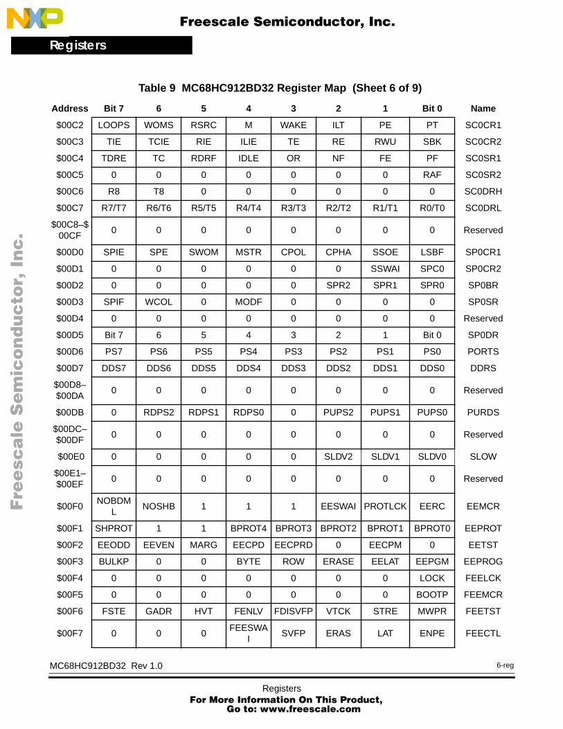
Registers
F
ree
sca
le S
em
ico
nd
uc
tor,
I
Freescale Semiconductor, Inc.n
c..
.
$00C2 LOOPS WOMS RSRC M WAKE ILT PE PT SC0CR1
$00C3 TIE TCIE RIE ILIE TE RE RWU SBK SC0CR2
$00C4 TDRE TC RDRF IDLE OR NF FE PF SC0SR1
$00C5 0 0 0 0 0 0 0 RAF SC0SR2
$00C6 R8 T8 0 0 0 0 0 0 SC0DRH
$00C7 R7/T7 R6/T6 R5/T5 R4/T4 R3/T3 R2/T2 R1/T1 R0/T0 SC0DRL
$00C8–$00CF
0 0 0 0 0 0 0 0 Reserved
$00D0 SPIE SPE SWOM MSTR CPOL CPHA SSOE LSBF SP0CR1
$00D1 0 0 0 0 0 0 SSWAI SPC0 SP0CR2
$00D2 0 0 0 0 0 SPR2 SPR1 SPR0 SP0BR
$00D3 SPIF WCOL 0 MODF 0 0 0 0 SP0SR
$00D4 0 0 0 0 0 0 0 0 Reserved
$00D5 Bit 7 6 5 4 3 2 1 Bit 0 SP0DR
$00D6 PS7 PS6 PS5 PS4 PS3 PS2 PS1 PS0 PORTS
$00D7 DDS7 DDS6 DDS5 DDS4 DDS3 DDS2 DDS1 DDS0 DDRS
$00D8– $00DA
0 0 0 0 0 0 0 0 Reserved
$00DB 0 RDPS2 RDPS1 RDPS0 0 PUPS2 PUPS1 PUPS0 PURDS
$00DC– $00DF
0 0 0 0 0 0 0 0 Reserved
$00E0 0 0 0 0 0 SLDV2 SLDV1 SLDV0 SLOW
$00E1– $00EF
0 0 0 0 0 0 0 0 Reserved
$00F0NOBDM
LNOSHB 1 1 1 EESWAI PROTLCK EERC EEMCR
$00F1 SHPROT 1 1 BPROT4 BPROT3 BPROT2 BPROT1 BPROT0 EEPROT
$00F2 EEODD EEVEN MARG EECPD EECPRD 0 EECPM 0 EETST
$00F3 BULKP 0 0 BYTE ROW ERASE EELAT EEPGM EEPROG
$00F4 0 0 0 0 0 0 0 LOCK FEELCK
$00F5 0 0 0 0 0 0 0 BOOTP FEEMCR
$00F6 FSTE GADR HVT FENLV FDISVFP VTCK STRE MWPR FEETST
$00F7 0 0 0FEESWA
ISVFP ERAS LAT ENPE FEECTL
Table 9 MC68HC912BD32 Register Map (Sheet 6 of 9)
Address Bit 7 6 5 4 3 2 1 Bit 0 Name
MC68HC912BD32 Rev 1.0
Registers For More Information On This Prod
Go to: www.freescale.com
6-reg
uct,

RegistersIntroduction
MC68HC912BD32 Rev 1.0
F
ree
sca
le S
em
ico
nd
uc
tor,
I
Freescale Semiconductor, Inc.n
c..
.
7-reg
$00F8-$00FF
- - - - - - - - Reserved
$0100 SFTRES MASTER ALARM SLPRQ SLPACK WPULSE SSWAI 0 MCR
$0101 0 0 0 FSIZ4 FSIZ3 FSIZ2 FSIZ1 FSIZ0 FSIZR
$0102 TWX0T7 TWX0T6 TWX0T5 TWX0T4 TWX0T3 TWX0T2 TWX0T1 TWX0T0 TCR1
$0103 TWX0R7 TWX0R6 TWX0R5 TWX0R4 TWX0R3 TWX0R2 TWX0R1 TWX0R0 TCR2
$0104 TWXD7 TWXD6 TWXD5 TWXD4 TWXD3 TWXD2 TWXD1 TWXD0 TCR3
$0105 - - - - - - - - Reserved
$0106 RCVFIF RXIF SYNAIF SYNNIF 0 0 0 OPTDF RISR
$0107 TXIF OVRNIF ERRIF SYNEIF SYNLIF ILLPIF LOCKIF WAKEIF GISR
$0108 RCVFIE RXIE SYNAIE SYNNIE 0 0 0 0 RIER
$0109 TXIE OVRNIE ERRIE SYNEIE SYNLIE ILLPIE LOCKIE WAKEIE GIER
$010A 0 0 0 0 RIVEC3 RIVEC2 RIVEC1 RIVEC0 RIVEC
$010B 0 0 0 0 TIVEC3 TIVEC2 TIVEC1 TIVEC0 TIVEC
$010C FIDAC7 FIDAC6 FIDAC5 FIDAC4 FIDAC3 FIDAC2 FIDAC1 FIDAC0 FIDAC
$010D FIDMR7 FIDMR6 FIDMR5 FIDMR4 FIDMR3 FIDMR2 FIDMR1 FIDMR0 FIDMR
$010E MVR7 MVR6 MVR5 MVR4 MVR3 MVR2 MVR1 MVR0 MVR
$010F 0 0 0 0 0 0 0 TACC SITEST
$0110 0 0 0 PERREN PROKEN PSYNEN PUESBI RDRSBI PCTLSBI
$0111 DIVBYP PSBI6 PSBI5 PSBI4 PSBI3 PSBI2 TX RX PORTSBI
$0112 DDRSBI7 DDRSBI6 DDRSBI5 DDRSBI4 DDRSBI3 DDRSBI2 0 0 DDRSBI
$0113-$011F
- - - - - - - - Reserved
$0120 ID7 ID6 ID5 ID4 ID3 ID2 ID1 ID0 IDENTIFIER4
$0121 reserved reserved reserved reserved LEN3 LEN2 LEN1 LEN0 DATA LENGTH
$0122 D7 D6 D5 D4 D3 D2 D1 D0 DATA0
$0123 D7 D6 D5 D4 D3 D2 D1 D0 DATA1
$0124 D7 D6 D5 D4 D3 D2 D1 D0 DATA2
$0125 D7 D6 D5 D4 D3 D2 D1 D0 DATA3
$0126 D7 D6 D5 D4 D3 D2 D1 D0 DATA4
$0127 D7 D6 D5 D4 D3 D2 D1 D0 DATA5
$0128 D7 D6 D5 D4 D3 D2 D1 D0 DATA6
Table 9 MC68HC912BD32 Register Map (Sheet 7 of 9)
Address Bit 7 6 5 4 3 2 1 Bit 0 Name
Registers For More Information On This Product,
Go to: www.freescale.com

Registers
F
ree
sca
le S
em
ico
nd
uc
tor,
I
Freescale Semiconductor, Inc.n
c..
.
$0129 D7 D6 D5 D4 D3 D2 D1 D0 DATA7
$012A D7 D6 D5 D4 D3 D2 D1 D0 DATA8
$012B D7 D6 D5 D4 D3 D2 D1 D0 DATA9
$012C D7 D6 D5 D4 D3 D2 D1 D0 DATA10
$012D D7 D6 D5 D4 D3 D2 D1 D0 DATA11
$012E-$012F
- - - - - - - - Reserved
$0130 ID7 ID6 ID5 ID4 ID3 ID2 ID1 ID0 IDENTIFIER5
$0131 reserved reserved reserved reserved LEN3 LEN2 LEN1 LEN0 DATA LENGTH
$0132 D7 D6 D5 D4 D3 D2 D1 D0 DATA0
$0133 D7 D6 D5 D4 D3 D2 D1 D0 DATA1
$0134 D7 D6 D5 D4 D3 D2 D1 D0 DATA2
$0135 D7 D6 D5 D4 D3 D2 D1 D0 DATA3
$0136 D7 D6 D5 D4 D3 D2 D1 D0 DATA4
$0137 D7 D6 D5 D4 D3 D2 D1 D0 DATA5
$0138 D7 D6 D5 D4 D3 D2 D1 D0 DATA6
$0139 D7 D6 D5 D4 D3 D2 D1 D0 DATA7
$013A D7 D6 D5 D4 D3 D2 D1 D0 DATA8
$013B D7 D6 D5 D4 D3 D2 D1 D0 DATA9
$013C D7 D6 D5 D4 D3 D2 D1 D0 DATA10
$013D D7 D6 D5 D4 D3 D2 D1 D0 DATA11
$013E-$013F
- - - - - - - - Reserved
$0140 ID7 ID6 ID5 ID4 ID3 ID2 ID1 ID0 IDENTIFIER6
$0141 reserved reserved reserved reserved LEN3 LEN2 LEN1 LEN0 DATA LENGTH
$0142 D7 D6 D5 D4 D3 D2 D1 D0 DATA0
$0143 D7 D6 D5 D4 D3 D2 D1 D0 DATA1
$0144 D7 D6 D5 D4 D3 D2 D1 D0 DATA2
$0145 D7 D6 D5 D4 D3 D2 D1 D0 DATA3
$0146 D7 D6 D5 D4 D3 D2 D1 D0 DATA4
$0147 D7 D6 D5 D4 D3 D2 D1 D0 DATA5
$0148 D7 D6 D5 D4 D3 D2 D1 D0 DATA6
Table 9 MC68HC912BD32 Register Map (Sheet 8 of 9)
Address Bit 7 6 5 4 3 2 1 Bit 0 Name
MC68HC912BD32 Rev 1.0
Registers For More Information On This Prod
Go to: www.freescale.com
8-reg
uct,

RegistersIntroduction
MC68HC912BD32 Rev 1.0
F
ree
sca
le S
em
ico
nd
uc
tor,
I
Freescale Semiconductor, Inc.n
c..
.
9-reg
$0149 D7 D6 D5 D4 D3 D2 D1 D0 DATA7
$014A D7 D6 D5 D4 D3 D2 D1 D0 DATA8
$014B D7 D6 D5 D4 D3 D2 D1 D0 DATA9
$014C D7 D6 D5 D4 D3 D2 D1 D0 DATA10
$014D D7 D6 D5 D4 D3 D2 D1 D0 DATA11
$014E-$014F
- - - - - - - - Reserved
$0150 IFLG IENA LOCK 0 0 0 0 CFG BUFCTL0
$0151 IFLG IENA LOCK 0 0 0 0 CFG BUFCTL1
$0152 IFLG IENA LOCK 0 0 0 0 CFG BUFCTL2
$0153 IFLG IENA LOCK 0 0 0 0 CFG BUFCTL3
$0154 IFLG IENA LOCK 0 0 0 0 CFG BUFCTL4
$0155 IFLG IENA LOCK 0 0 0 0 CFG BUFCTL5
$0156 IFLG IENA LOCK 0 0 0 0 CFG BUFCTL6
$0157 IFLG IENA LOCK 0 0 0 0 CFG BUFCTL7
$0158 IFLG IENA LOCK 0 0 0 0 CFG BUFCTL8
$0159 IFLG IENA LOCK 0 0 0 0 CFG BUFCTL9
$015A IFLG IENA LOCK 0 0 0 0 CFG BUFCTL10
$015B IFLG IENA LOCK 0 0 0 0 CFG BUFCTL11
$015C IFLG IENA LOCK 0 0 0 0 CFG BUFCTL12
$015D IFLG IENA LOCK 0 0 0 0 CFG BUFCTL13
$015E IFLG IENA LOCK 0 0 0 0 CFG BUFCTL14
$015F IFLG IENA LOCK 0 0 0 0 CFG BUFCTL15
1. Port A, port B, and data direction registers DDRA and DDRB are not in map in expanded and peripheral modes.2. Port E and DDRE not in map in peripheral mode; also not in map in expanded modes with EME set.3. Not in map in peripheral mode.4. $0120-$012D: Byteflight™ Active Transmit Buffer Register5. $0130-$013D: Byteflight™ Active Receive Buffer Register6. $0140-$014D: Byteflight™ Active FIFO Register
Table 9 MC68HC912BD32 Register Map (Sheet 9 of 9)
Address Bit 7 6 5 4 3 2 1 Bit 0 Name
Registers For More Information On This Product,
Go to: www.freescale.com

Registers
F
ree
sca
le S
em
ico
nd
uc
tor,
I
Freescale Semiconductor, Inc.n
c..
.
MC68HC912BD32 Rev 1.0
Registers For More Information On This Prod
Go to: www.freescale.com
10-reg
uct,

F
ree
sca
le S
em
ico
nd
uc
tor,
IFreescale Semiconductor, Inc.
nc
...
Operating Modes and Resource MappingOperating Modes and Resource Mapping
Contents
Introduction . . . . . . . . . . . . . . . . . . . . . . . . . . . . . . . . . . . . . . . . . . . . . 43Operating Modes. . . . . . . . . . . . . . . . . . . . . . . . . . . . . . . . . . . . . . . . . 43Background Debug Mode . . . . . . . . . . . . . . . . . . . . . . . . . . . . . . . . . . 46Internal Resource Mapping . . . . . . . . . . . . . . . . . . . . . . . . . . . . . . . . . 49Memory Maps . . . . . . . . . . . . . . . . . . . . . . . . . . . . . . . . . . . . . . . . . . . 53
Introduction
Eight possible operating modes determine the operating configuration of the MC68HC912BD32. Each mode has an associated default memory map and external bus configuration. After reset, most system resources can be mapped to other addresses by writing to the appropriate control registers.
Operating Modes
The operating mode out of reset is determined by the states of the BKGD, MODB, and MODA pins during reset.
The SMODN, MODB, and MODA bits in the MODE register show current operating mode and provide limited mode switching during operation. The states of the BKGD, MODB, and MODA pins are latched into these bits on the rising edge of the reset signal. During reset an active pullup is connected to the BKGD pin (as input) and active pulldowns are connected to the MODB and MODA pins. If an open occurs on any of these pins, the device will operate in normal single-chip mode.
MC68HC912BD32 Rev 1.0
1-modeOperating Modes and Resource Mapping For More Information On This Product,
Go to: www.freescale.com

Operating Modes and Resource Mapping
F
ree
sca
le S
em
ico
nd
uc
tor,
I
Freescale Semiconductor, Inc.n
c..
.
There are two basic types of operating modes:
Normal modes — some registers and bits are protected against accidental changes.
Special modes — allow greater access to protected control registers and bits for special purposes such as testing and emulation.
A system development and debug feature, background debug mode (BDM), is available in all modes. In special single-chip mode, BDM is active immediately after reset.
Normal Operating Modes
These modes provide three operating configurations. Background debugging is available in all three modes, but must first be enabled for some operations by means of a BDM command. BDM can then be made active by another BDM command.
Normal Expanded Wide Mode
This is a normal mode of operation in which the address and data are multiplexed onto ports A and B. ADDR[15:8] and DATA[15:8] are present on port A. ADDR[7:0] and DATA[7:0] are present on port B.
Normal Expanded Narrow Mode
Port A is configured as the high byte of address multiplexed with the 8-bit data bus. Port B is configured as the lower 8-bit address bus. This mode is used for lower cost production systems that use 8-bit wide external EEPROMs or RAMs. Such systems take extra bus cycles to access
Table 10 Mode Selection
BKGD MODB MODA Mode Port A Port B
0 0 0 Special Single Chip General Purpose I/O General Purpose I/O
0 0 1 Special Expanded Narrow ADDR[15:8]/DATA[7:0] ADDR[7:0]
0 1 0 Special Peripheral ADDR/DATA ADDR/DATA
0 1 1 Special Expanded Wide ADDR/DATA ADDR/DATA
1 0 0 Normal Single Chip General Purpose I/O General Purpose I/O
1 0 1 Normal Expanded Narrow ADDR[15:8]/DATA[7:0] ADDR[7:0]
1 1 0 Reserved (Forced to Peripheral) — —
1 1 1 Normal Expanded Wide ADDR/DATA ADDR/DATA
MC68HC912BD32 Rev 1.0
Operating Modes and Resource Mappin For More Information On This Prod
Go to: www.freescale.com
2-mode
guct,
Operating Modes and Resource MappingOperating Modes
F
ree
sca
le S
em
ico
nd
uc
tor,
I
Freescale Semiconductor, Inc.n
c..
.
16-bit locations but this may be preferred over the extra cost of additional external memory devices.
Normal Single-Chip Mode
There are no external address and data buses in this mode. All pins of ports A, B and E are configured as general-purpose I/O pins. Port E bits 1 and 0 are input-only with internal pullups and the other 22 pins are bidirectional I/O pins that are initially configured as high-impedance inputs. Port E pullups are enabled upon reset; port A and B pullups are disabled upon reset.
Special Operating Modes
There are three special operating modes that correspond to normal operating modes. These operating modes are commonly used in factory testing and system development. In addition, there is a special peripheral mode, in which an external master, such as an I.C. tester, can control the on-chip peripherals.
Special Expanded Wide Mode
This mode can be used for emulation of normal expanded wide mode and emulation of normal single-chip mode and 16-bit data bus. The bus control related pins in PORTE are all configured to serve their bus control output functions rather than general-purpose I/O.
Special Expanded Narrow Mode
This mode can be used for emulation of normal expanded narrow mode. In this mode external 16-bit data is handled as two back-to-back bus cycles, one for the high byte followed by one for the low byte. Internal operations continue to use full 16-bit data paths.
Special Single-Chip Mode
This mode can be used to force the MCU to active BDM mode to allow system debug through the BKGD pin. The MCU does not fetch the reset vector and execute application code as it would in other modes. Instead, the active background mode is in control of CPU execution and BDM firmware is waiting for additional serial commands through the BKGD pin. There are no external address and data buses in this mode. The MCU operates as a stand-alone device and all program and data space are on-chip. External port pins can be used for general-purpose I/O.
MC68HC912BD32 Rev 1.0
3-modeOperating Modes and Resource Mapping For More Information On This Product,
Go to: www.freescale.com

Operating Modes and Resource Mapping
F
ree
sca
le S
em
ico
nd
uc
tor,
I
Freescale Semiconductor, Inc.n
c..
.
Special Peripheral Mode
The CPU is not active in this mode. An external master can control on-chip peripherals for testing purposes. It is not possible to change to or from this mode without going through reset. Background debugging should not be used while the MCU is in special peripheral mode as internal bus conflicts between BDM and the external master can cause improper operation of both modes.
Background Debug Mode
Background debug mode (BDM) is an auxiliary operating mode that is used for system development. BDM is implemented in on-chip hardware and provides a full set of debug operations. Some BDM commands can be executed while the CPU is operating normally. Other BDM commands are firmware based, and require the BDM firmware to be enabled and active for execution.
In special single-chip mode, BDM is enabled and active immediately out of reset. BDM is available in all other operating modes, but must be enabled before it can be activated. BDM should not be used in special peripheral mode because of potential bus conflicts.
Once enabled, background mode can be made active by a serial command sent via the BKGD pin or execution of a CPU12 BGND instruction. While background mode is active, the CPU can interpret special debugging commands, and read and write CPU registers, peripheral registers, and locations in memory.
While BDM is active, the CPU executes code located in a small on-chip ROM mapped to addresses $FF00 to $FFFF; BDM control registers are accessible at addresses $FF00 to $FF06. The BDM ROM replaces the regular system vectors while BDM is active. While BDM is active, the user memory from $FF00 to $FFFF is not in the map except through serial BDM commands.
BDM allows read and write access to internal memory-mapped registers and RAM, and read access to EEPROM and Flash EEPROM without interrupting the application code executing in the CPU. This non-intrusive mode uses dead bus cycles to access the memory and in
MC68HC912BD32 Rev 1.0
Operating Modes and Resource Mappin For More Information On This Prod
Go to: www.freescale.com
4-mode
guct,
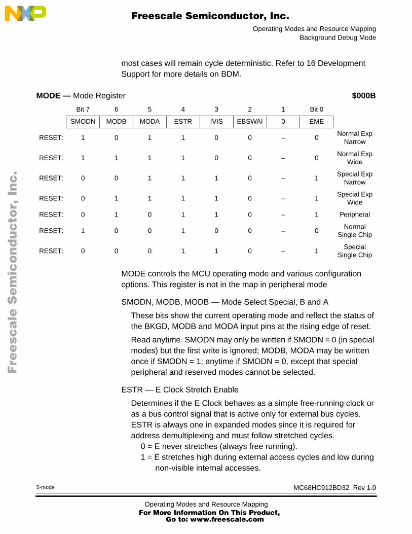
Operating Modes and Resource MappingBackground Debug Mode
F
ree
sca
le S
em
ico
nd
uc
tor,
I
Freescale Semiconductor, Inc.n
c..
.
most cases will remain cycle deterministic. Refer to 16 Development Support for more details on BDM.
MODE controls the MCU operating mode and various configuration options. This register is not in the map in peripheral mode
SMODN, MODB, MODB — Mode Select Special, B and A
These bits show the current operating mode and reflect the status of the BKGD, MODB and MODA input pins at the rising edge of reset.
Read anytime. SMODN may only be written if SMODN = 0 (in special modes) but the first write is ignored; MODB, MODA may be written once if SMODN = 1; anytime if SMODN = 0, except that special peripheral and reserved modes cannot be selected.
ESTR — E Clock Stretch Enable
Determines if the E Clock behaves as a simple free-running clock or as a bus control signal that is active only for external bus cycles. ESTR is always one in expanded modes since it is required for address demultiplexing and must follow stretched cycles.
0 = E never stretches (always free running).1 = E stretches high during external access cycles and low during
non-visible internal accesses.
MODE — Mode Register $000B
Bit 7 6 5 4 3 2 1 Bit 0
SMODN MODB MODA ESTR IVIS EBSWAI 0 EME
RESET: 1 0 1 1 0 0 – 0Normal Exp
Narrow
RESET: 1 1 1 1 0 0 – 0Normal Exp
Wide
RESET: 0 0 1 1 1 0 – 1Special Exp
Narrow
RESET: 0 1 1 1 1 0 – 1Special Exp
Wide
RESET: 0 1 0 1 1 0 – 1 Peripheral
RESET: 1 0 0 1 0 0 – 0Normal
Single Chip
RESET: 0 0 0 1 1 0 – 1Special
Single Chip
MC68HC912BD32 Rev 1.0
5-modeOperating Modes and Resource Mapping For More Information On This Product,
Go to: www.freescale.com

Operating Modes and Resource Mapping
F
ree
sca
le S
em
ico
nd
uc
tor,
I
Freescale Semiconductor, Inc.n
c..
.
Normal modes: write once; Special modes: write anytime, read anytime.
IVIS — Internal Visibility
This bit determines whether internal ADDR/DATA, R/W, and LSTRB signals can be seen on the bus during accesses to internal locations. In special expanded narrow mode, it is possible to configure the MCU to show internal accesses on an external 16-bit bus. The IVIS control bit must be set to 1. When the system is configured this way, visible internal accesses are shown as if the MCU was configured for expanded wide mode but normal external accesses operate as if the bus was in narrow mode. In normal expanded narrow mode, internal visibility is not allowed and IVIS is ignored.
0 = No visibility of internal bus operations on external bus1 = Internal bus operations are visible on external bus
Normal modes: write once; Special modes: write anytime EXCEPT the first time. Read anytime.
EBSWAI — External Bus Module Stop in Wait Control
This bit controls access to the external bus interface when in Wait mode. The module will delay before shutting down in Wait mode to allow for final bus activity to complete.
0 = External bus and registers continue functioning during Wait mode.
1 = External bus is shut down during Wait mode.
EME — Emulate Port E
Removing the registers from the map allows the user to emulate the function of these registers externally. In single-chip mode PORTE and DDRE are always in the map regardless of the state of this bit.
0 = PORTE and DDRE are in the memory map.1 = PORTE and DDRE are removed from the internal memory map
(expanded mode).
Normal modes: write once; special modes: write anytime EXCEPT the first time. Read anytime.
MC68HC912BD32 Rev 1.0
Operating Modes and Resource Mappin For More Information On This Prod
Go to: www.freescale.com
6-mode
guct,

Operating Modes and Resource MappingInternal Resource Mapping
MC68HC912BD32 Rev 1.0
F
ree
sca
le S
em
ico
nd
uc
tor,
I
Freescale Semiconductor, Inc.n
c..
.
7-mode
Internal Resource Mapping
The internal register block, RAM, Flash EEPROM and EEPROM have default locations within the 64K byte standard address space but may be reassigned to other locations during program execution by setting bits in mapping registers INITRG, INITRM, and INITEE. During normal operating modes these registers can be written once. It is advisable to explicitly establish these resource locations during the initialization phase of program execution, even if default values are chosen, in order to protect the registers from inadvertent modification later.
Writes to the mapping registers go into effect between the cycle that follows the write and the cycle after that. To assure that there are no unintended operations, a write to one of these registers should be followed with a NOP instruction.
If conflicts occur when mapping resources, the register block will take precedence over the other resources; RAM, Flash EEPROM, or EEPROM addresses occupied by the register block will not be available for storage. When active, BDM ROM takes precedence over other resources although a conflict between BDM ROM and register space is not possible. Table 11 shows resource mapping precedence.
All address space not utilized by internal resources is by default external memory.
Register Block Mapping
After reset the 512 byte register block resides at location $0000 but can be reassigned to any 2K byte boundary within the standard 64K byte address space. Mapping of internal registers is controlled by five bits in
Table 11 Mapping Precedence
Precedence Resource
1 BDM ROM (if active)
2 Register Space
3 RAM
4 EEPROM
5 Flash EEPROM
6 External Memory
Operating Modes and Resource Mapping For More Information On This Product,
Go to: www.freescale.com

Operating Modes and Resource Mapping
F
ree
sca
le S
em
ico
nd
uc
tor,
I
Freescale Semiconductor, Inc.n
c..
.
the INITRG register. The register block occupies the first 512 bytes of the 2K byte block.
REG[15:11] — Internal register map position
These bits specify the upper five bits of the 16-bit registers address.
Write once in normal modes or anytime in special modes. Read anytime.
MMSWAI — Memory Mapping Interface Stop in Wait Control
This bit controls access to the memory mapping interface when in Wait mode.
0 = Memory mapping interface continues to function during Wait mode.
1 = Memory mapping interface access is shut down during Wait mode.
RAM Mapping
The MC68HC912BD32 has 1K byte of fully static RAM that is used for storing instructions, variables, and temporary data during program execution. After reset, RAM addressing begins at location $0800 but can be assigned to any 2K byte boundary within the standard 64K byte address space. Mapping of internal RAM is controlled by five bits in the INITRM register. The RAM array occupies the first 1K byte of the 2K byte block.
RAM[15:11] — Internal RAM map position
These bits specify the upper five bits of the 16-bit RAM address.
INITRG — Initialization of Internal Register Position Register $0011
Bit 7 6 5 4 3 2 1 Bit 0
REG15 REG14 REG13 REG12 REG11 0 0 MMSWAI
RESET: 0 0 0 0 0 0 0 0
NITRM — Initialization of Internal RAM Position Register $0010
Bit 7 6 5 4 3 2 1 Bit 0
RAM15 RAM14 RAM13 RAM12 RAM11 0 0 0
RESET: 0 0 0 0 1 0 0 0
MC68HC912BD32 Rev 1.0
Operating Modes and Resource Mappin For More Information On This Prod
Go to: www.freescale.com
8-mode
guct,

Operating Modes and Resource MappingInternal Resource Mapping
MC68HC912BD32 Rev 1.0
F
ree
sca
le S
em
ico
nd
uc
tor,
I
Freescale Semiconductor, Inc.n
c..
.
9-mode
Write once in normal modes or anytime in special modes. Read anytime.
EEPROM Mapping The MC68HC912BD32 has 768 bytes of EEPROM which is activated by the EEON bit in the INITEE register.
Mapping of internal EEPROM is controlled by four bits in the INITEE register. After reset EEPROM address space begins at location $0D00 but can be mapped to any 4K byte boundary within the standard 64K byte address space.
EE[15:12] — Internal EEPROM map position
These bits specify the upper four bits of the 16-bit EEPROM address.
Write once in normal modes or anytime in special modes. Read anytime.
EEON — Internal EEPROM On (Enabled)
The EEON bit allows read access to the EEPROM array. EEPROM control registers can be accessed and EEPROM locations may be programmed or erased regardless of the state of EEON.
This bit is forced to one in single-chip modes. Read or write anytime.0 = Removes the EEPROM from the map1 = Places the on-chip EEPROM in the memory map
Flash EEPROM and Expansion Address Mapping
Additional mapping controls are available that can be used in conjunction with Flash EEPROM and memory expansion.
The 32K byte Flash EEPROM can be mapped to either the upper or lower half of the 64K byte address space. When mapping conflicts occur, registers, RAM and EEPROM have priority over Flash EEPROM. To use memory expansion the part must be operated in one of the expanded modes.
INITEE— Initialization of Internal EEPROM Position Register $0012
Bit 7 6 5 4 3 2 1 Bit 0
EE15 EE14 EE13 EE12 0 0 0 EEON
RESET: 0 0 0 0 0 0 0 1
Operating Modes and Resource Mapping For More Information On This Product,
Go to: www.freescale.com

Operating Modes and Resource Mapping
F
ree
sca
le S
em
ico
nd
uc
tor,
I
Freescale Semiconductor, Inc.n
c..
.
This register can be read anytime. In Normal modes MISC can be written once; in Special modes it can be written anytime.
NDRF — Narrow Data Bus for Register-Following Map
This bit enables a narrow bus feature for the 512-byte register-following map. In Expanded Narrow (eight bit) modes, Single Chip modes, and Peripheral mode, NDRF has no effect. The register-following map always begins at the byte following the 512-byte register map. If the registers are moved this space will also move.
0 = Register-following map space acts as a full 16-bit data bus1 = Register-following map space acts the same as an 8-bit
external data bus
RFSTR1, RFSTR0 — Register-Following Stretch Bit 1 and Bit 0
These bits determine the amount of clock stretch on accesses to the 512-byte register-following map. It is valid regardless of the state of the NDRF bit. In Single Chip and Peripheral modes this bit has no meaning or effect.
EXSTR1, EXSTR0 — External Access Stretch Bit1 and Bit0
These bits determine the amount of clock stretch on accesses to the external address space. In Single Chip and Peripheral modes this bit has no meaning or effect.
MISC — Miscellaneous Mapping Control Register $0013
Bit 7 6 5 4 3 2 1 Bit 0
0 NDRF RFSTR1 RFSTR0 EXSTR1 EXSTR0 MAPROM ROMON
RESET: 0 0 0 0 1 1 0 0 Ex. mode
0 0 0 0 1 1 1 1SIngle-chip mode
Table 12 Register-Following Stretch-Bit Definition
Stretch bit RFSTR1 Stretch bit RFSTR0 E Clocks Stretched
0 0 0
0 1 1
1 0 2
1 1 3
MC68HC912BD32 Rev 1.0
Operating Modes and Resource Mappin For More Information On This Prod
Go to: www.freescale.com
10-mode
guct,

Operating Modes and Resource MappingMemory Maps
MC68HC912BD32 Rev 1.0
F
ree
sca
le S
em
ico
nd
uc
tor,
I
Freescale Semiconductor, Inc.n
c..
.
11-mode
MAPROM — Map Location of Flash EEPROM
This bit determines the location of the on-chip Flash EEPROM. In Expanded modes it is reset to zero. In Single Chip modes it is reset to one. If ROMON is zero, this bit has no meaning or effect.
0 = Flash EEPROM is located from $0000 to $7FFF1 = Flash EEPROM is located from $8000 to $FFFF
ROMON — Enable Flash EEPROM
In Expanded modes ROMON is reset to zero. In Single Chip modes it is reset to one. If the internal RAM, registers, EEPROM, or BDM ROM (if active) are mapped to the same space as the Flash EEPROM, they will have priority over the Flash EEPROM.
0 = Disables the Flash EEPROM in the memory map1 = Enables the Flash EEPROM in the memory map
Memory Maps
The following diagrams illustrate the memory map for each mode of operation immediately after reset.
Table 13 Expanded Stretch-Bit Definition
Stretch bit EXSTR1 Stretch bit EXSTR0 E Clocks Stretched
0 0 0
0 1 1
1 0 2
1 1 3
Operating Modes and Resource Mapping For More Information On This Product,
Go to: www.freescale.com

Operating Modes and Resource Mapping
F
ree
sca
le S
em
ico
nd
uc
tor,
I
Freescale Semiconductor, Inc.n
c..
.
Figure 6 MC68HC912BD32 Memory Map
BDM(IF ACTIVE)
$8000
$FFFF$FFFF
FLASH EEPROM
$0000
$0800
$0D00
$0FFF
$FF00
$0000
$01FF
$0800
SINGLE CHIPSPECIAL
SINGLE CHIPNORMAL
EXPANDED
$8000
VECTORS VECTORS VECTORS
$FF00$F000
768 BYTES EEPROMMAP TO ANY 4K SPACE
1K byte RAMMAP TO ANY 2K SPACE
REGISTERS
MAP TO ANY 2K SPACE
$FFFF$FFC0
$0BFF
MAP WITH MAPROM BIT
$0D00
512 BYTES RAM$0000
$7FFF
IN MISC REGISTERTO $0000 – $7FFFOR $8000 – $FFFF
$0200
$03FF
REGISTER FOLLOWINGSPACE512 BYTES RAM
MC68HC912BD32 Rev 1.0
Operating Modes and Resource Mappin For More Information On This Prod
Go to: www.freescale.com
12-mode
guct,

F
ree
sca
le S
em
ico
nd
uc
tor,
IFreescale Semiconductor, Inc.
nc
...
Bus Control and Input/Output
Bus Control and Input/Output
Contents
Introduction . . . . . . . . . . . . . . . . . . . . . . . . . . . . . . . . . . . . . . . . . . . . . 55Detecting Access Type from External Signals . . . . . . . . . . . . . . . . . . 55Registers . . . . . . . . . . . . . . . . . . . . . . . . . . . . . . . . . . . . . . . . . . . . . . . 56
Introduction
Internally the MC68HC912BD32 has full 16-bit data paths, but depending upon the operating mode and control registers, the external bus may be 8 or 16 bits. There are cases where 8-bit and 16-bit accesses can appear on adjacent cycles using the LSTRB signal to indicate 8- or 16-bit data.
Detecting Access Type from External Signals
The external signals LSTRB, R/W, and A0 can be used to determine the type of bus access that is taking place. Accesses to the internal RAM module are the only type of access that produce LSTRB=A0=1, because the internal RAM is specifically designed to allow misaligned 16-bit accesses in a single cycle. In these cases the data for the address that was accessed is on the low half of the data bus and the data for address + 1 is on the high half of the data bus (data order is swapped).
MC68HC912BD32 Rev 1.0
1-busBus Control and Input/Output For More Information On This Product,
Go to: www.freescale.com

Bus Control and Input/Output
F
ree
sca
le S
em
ico
nd
uc
tor,
I
Freescale Semiconductor, Inc.n
c..
.
Registers
Not all registers are visible in the MC68HC912BD32 memory map under certain conditions. In special peripheral mode the first 16 registers associated with bus expansion are removed from the memory map.
In expanded modes, some or all of port A, port B, and port E are used for expansion buses and control signals. In order to allow emulation of the single-chip functions of these ports, some of these registers must be rebuilt in an external port replacement unit. In any expanded mode port A and port B are used for address and data lines so registers for these ports, as well as the data direction registers for these ports, are removed from the on-chip memory map and become external accesses.
In any expanded mode, port E pins may be needed for bus control (e.g., ECLK, R/W). To regain the single-chip functions of port E, the emulate port E (EME) control bit in the MODE register may be set. In this special case of expanded mode and EME set, PORTE and DDRE registers are removed from the on-chip memory map and become external accesses so port E may be rebuilt externally.
Table 14 Access Type vs. Bus Control Pins
LSTRB A0 R/W Type of Access
1 0 1 8-bit read of an even address
0 1 1 8-bit read of an odd address
1 0 0 8-bit write of an even address
0 1 0 8-bit write of an odd address
0 0 1 16-bit read of an even address
1 1 116-bit read of an odd address(low/high data swapped)
0 0 0 16-bit write to an even address
1 1 016-bit write to an odd address(low/high data swapped)
MC68HC912BD32 Rev 1.0
Bus Control and Input/Output For More Information On This Prod
Go to: www.freescale.com
2-bus
uct,

Bus Control and Input/OutputRegisters
F
ree
sca
le S
em
ico
nd
uc
tor,
I
Freescale Semiconductor, Inc.n
c..
.
Bits PA[7:0] are associated with addresses ADDR[15:8] and DATA[15:8]. When this port is not used for external addresses and data, such as in single-chip mode, these pins can be used as general-purpose I/O. DDRA determines the primary direction of each pin. This register is not in the on-chip map in expanded and peripheral modes. Read and write anytime.
This register determines the primary direction for each port A pin when functioning as a general-purpose I/O port. DDRA is not in the on-chip map in expanded and peripheral modes. Read and write anytime.
0 = Associated pin is a high-impedance input1 = Associated pin is an output
PORTA —
Port A Register
$0000
Bit 7 6 5 4 3 2 1 Bit 0
Single Chip PA7 PA6 PA5 PA4 PA3 PA2 PA1 PA0
RESET: – – – – – – – –
Exp Wide& Periph:
ADDR15DATA15
ADDR14DATA14
ADDR13DATA13
ADDR12DATA12
ADDR11DATA11
ADDR10DATA10
ADDR9DATA9
ADDR8DATA8
Expanded Narrow
ADDR15DATA15/7
ADDR14DATA14/6
ADDR13DATA13/5
ADDR12DATA12/4
ADDR11DATA11/3
ADDR10DATA10/2
ADDR9DATA9/1
ADDR8DATA8/0
DDRA —
Port A Data Direction Register
$0002
Bit 7 6 5 4 3 2 1 Bit 0
DDA7 DDA6 DDA5 DDA4 DDA3 DDA2 DDA1 DDA0
RESET: 0 0 0 0 0 0 0 0
PORTB —
Port B Register
$0001
Bit 7 6 5 4 3 2 1 Bit 0
Single Chip PB7 PB6 PB5 PB4 PB3 PB2 PB1 PB0
RESET: – – – – – – – –
Exp Wide& Periph:
ADDR7DATA7
ADDR6DATA6
ADDR5DATA5
ADDR4DATA4
ADDR3DATA3
ADDR2DATA2
ADDR1DATA1
ADDR0DATA0
Expanded Narrow
ADDR7 ADDR6 ADDR5 ADDR4 ADDR3 ADDR2 ADDR1 ADDR0
MC68HC912BD32 Rev 1.0
3-busBus Control and Input/Output For More Information On This Product,
Go to: www.freescale.com
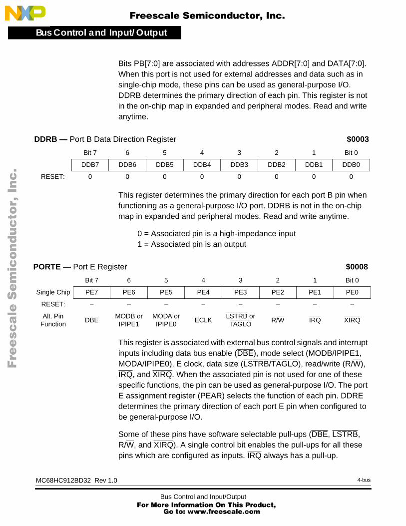
Bus Control and Input/Output
F
ree
sca
le S
em
ico
nd
uc
tor,
I
Freescale Semiconductor, Inc.n
c..
.
Bits PB[7:0] are associated with addresses ADDR[7:0] and DATA[7:0]. When this port is not used for external addresses and data such as in single-chip mode, these pins can be used as general-purpose I/O. DDRB determines the primary direction of each pin. This register is not in the on-chip map in expanded and peripheral modes. Read and write anytime.
This register determines the primary direction for each port B pin when functioning as a general-purpose I/O port. DDRB is not in the on-chip map in expanded and peripheral modes. Read and write anytime.
0 = Associated pin is a high-impedance input1 = Associated pin is an output
This register is associated with external bus control signals and interrupt inputs including data bus enable (DBE), mode select (MODB/IPIPE1, MODA/IPIPE0), E clock, data size (LSTRB/TAGLO), read/write (R/W), IRQ, and XIRQ. When the associated pin is not used for one of these specific functions, the pin can be used as general-purpose I/O. The port E assignment register (PEAR) selects the function of each pin. DDRE determines the primary direction of each port E pin when configured to be general-purpose I/O.
Some of these pins have software selectable pull-ups (DBE, LSTRB, R/W, and XIRQ). A single control bit enables the pull-ups for all these pins which are configured as inputs. IRQ always has a pull-up.
DDRB —
Port B Data Direction Register
$0003
Bit 7 6 5 4 3 2 1 Bit 0
DDB7 DDB6 DDB5 DDB4 DDB3 DDB2 DDB1 DDB0
RESET: 0 0 0 0 0 0 0 0
PORTE —
Port E Register
$0008
Bit 7 6 5 4 3 2 1 Bit 0
Single Chip PE7 PE6 PE5 PE4 PE3 PE2 PE1 PE0
RESET: – – – – – – – –
Alt. Pin Function
DBEMODB or IPIPE1
MODA or IPIPE0
ECLKLSTRB or
TAGLOR/W IRQ XIRQ
MC68HC912BD32 Rev 1.0
Bus Control and Input/Output For More Information On This Prod
Go to: www.freescale.com
4-bus
uct,

Bus Control and Input/OutputRegisters
F
ree
sca
le S
em
ico
nd
uc
tor,
I
Freescale Semiconductor, Inc.n
c..
.
This register is not in the map in peripheral mode or expanded modes when the EME bit is set.
Read and write anytime.
This register determines the primary direction for each port E pin configured as general-purpose I/O.
0 = Associated pin is a high-impedance input1 = Associated pin is an output
PE[1:0] are associated with XIRQ and IRQ and cannot be configured as outputs. These pins can be read regardless of whether the alternate interrupt functions are enabled.
This register is not in the map in peripheral mode and expanded modes while the EME control bit is set.
Read and write anytime.
The PEAR register is used to choose between the general-purpose I/O functions and the alternate bus control functions of port E. When an
DDRE —
Port E Data Direction Register
$0009
Bit 7 6 5 4 3 2 1 Bit 0
DDE7 DDE6 DDE5 DDE4 DDE3 DDE2 0 0
RESET: 0 0 0 0 0 0 – –
PEAR —
Port E Assignment Register
$000A
Bit 7 6 5 4 3 2 1 Bit 0
NDBE 0 PIPOE NECLK LSTRE RDWE 0 0
RESET: 0 – 0 0 0 0 – –Normal
Expanded
RESET: 0 – 1 0 1 1 – –Special
Expanded
RESET: 1 – 0 1 0 0 – – Peripheral
RESET: 1 – 0 1 0 0 – –Normal
Single Chip
RESET: 0 – 1 0 1 1 – –Special
Single Chip
MC68HC912BD32 Rev 1.0
5-busBus Control and Input/Output For More Information On This Product,
Go to: www.freescale.com

Bus Control and Input/Output
F
ree
sca
le S
em
ico
nd
uc
tor,
I
Freescale Semiconductor, Inc.n
c..
.
alternate control function is selected, the associated DDRE bits are overridden.
The reset condition of this register depends on the mode of operation because bus-control signals are needed immediately after reset in some modes.
In normal single-chip mode, no external bus control signals are needed so all of port E is configured for general-purpose I/O.
In special single-chip mode, the E clock is enabled as a timing reference and the other bits of port E are configured for general-purpose I/O.
In normal expanded modes, the reset vector is located in external memory. The E clock may be required for this access but R/W is only needed by the system when there are external writable resources. Therefore in normal expanded modes, only the E clock is configured for its alternate bus control function and the other bits of port E are configured for general-purpose I/O. If the normal expanded system needs any other bus-control signals, PEAR would need to be written before any access that needed the additional signals.
In special expanded modes, IPIPE1, IPIPE0, E, R/W, and LSTRB are configured as bus-control signals.
In peripheral mode, the PEAR register is not accessible for reads or writes.
NDBE — No Data Bus Enable
Read and write anytime.0 = PE7 is used for external control of data enables on memories.1 = PE7 is used for general-purpose I/O.
PIPOE — Pipe Signal Output Enable
Normal: write once; Special: write anytime except the first time. Read anytime.This bit has no effect in single chip modes.
0 = PE[6:5] are general-purpose I/O.1 = PE[6:5] are outputs and indicate the state of the instruction
queue.
MC68HC912BD32 Rev 1.0
Bus Control and Input/Output For More Information On This Prod
Go to: www.freescale.com
6-bus
uct,

Bus Control and Input/OutputRegisters
MC68HC912BD32 Rev 1.0
F
ree
sca
le S
em
ico
nd
uc
tor,
I
Freescale Semiconductor, Inc.n
c..
.
7-bus
NECLK — No External E Clock
In expanded modes, writes to this bit have no effect. E clock is required for de-multiplexing the external address; NECLK will remain zero in expanded modes. NECLK can be written once in normal single chip mode and can be written anytime in special single chip mode. The bit can be read anytime.
0 = PE4 is the external E-clock pin subject to the following limitation: In single-chip modes, PE4 is general-purpose I/O unless NECLK = 0 and either IVIS = 1 or ESTR = 0. A 16-bit write to PEAR:MODE can configure all three bits in one operation.
1 = PE4 is a general-purpose I/O pin.
LSTRE — Low Strobe (LSTRB) Enable
Normal: write once; Special: write anytime except the first time. Read anytime. This bit has no effect in single-chip modes or normal expanded narrow mode.
0 = PE3 is a general-purpose I/O pin.1 = PE3 is configured as the LSTRB bus-control output, provided
the MCU is not in single chip or normal expanded narrow modes.
LSTRB is used during external writes. After reset in normal expanded mode, LSTRB is disabled. If needed, it should be enabled before external writes. External reads do not normally need LSTRB because all 16 data bits can be driven even if the MCU only needs 8 bits of data.
TAGLO is a shared function of the PE3/LSTRB pin. In special expanded modes with LSTRE set and the BDM instruction tagging on, a zero at the falling edge of E tags the instruction word low byte being read into the instruction queue.
RDWE — Read/Write Enable
Normal: write once; Special: write anytime except the first time. Read anytime. This bit has no effect in single-chip modes.
0 = PE2 is a general-purpose I/O pin.1 = PE2 is configured as the R/W pin. In single chip modes, RDWE
has no effect and PE2 is a general-purpose I/O pin.
Bus Control and Input/Output For More Information On This Product,
Go to: www.freescale.com

Bus Control and Input/Output
F
ree
sca
le S
em
ico
nd
uc
tor,
I
Freescale Semiconductor, Inc.n
c..
.
R/W is used for external writes. After reset in normal expanded mode, it is disabled. If needed it should be enabled before any external writes.
These bits select pull-up resistors for any pin in the corresponding port that is currently configured as an input. This register is not in the map in peripheral mode.
Read and write anytime.
PUPE — Pull-Up Port E Enable
Pin PE1 always has a pull-up. Pins PE6, PE5, and PE4 never have pull-ups.
0 = Port E pull-ups on PE7, PE3, PE2, and PE0 are disabled.1 = Enable pull-up devices for port E input pins PE7, PE3, PE2, and
PE0.
PUPB — Pull-Up Port B Enable0 = Port B pull-ups are disabled.1 = Enable pull-up devices for all port B input pins.
This bit has no effect if port B is being used as part of the address/data bus (the pull-ups are inactive).
PUPA — Pull-Up Port A Enable0 = Port A pull-ups are disabled.1 = Enable pull-up devices for all port A input pins.
This bit has no effect if port A is being used as part of the address/data bus (the pull-ups are inactive).
PUCR — Pull Up Control Register $000C
Bit 7 6 5 4 3 2 1 Bit 0
0 0 0 PUPE 0 0 PUPB PUPA
RESET: 0 0 0 1 0 0 0 0
MC68HC912BD32 Rev 1.0
Bus Control and Input/Output For More Information On This Prod
Go to: www.freescale.com
8-bus
uct,

Bus Control and Input/OutputRegisters
MC68HC912BD32 Rev 1.0
F
ree
sca
le S
em
ico
nd
uc
tor,
I
Freescale Semiconductor, Inc.n
c..
.
9-bus
These bits select reduced drive for the associated port pins. This gives reduced power consumption and reduced RFI with a slight increase in transition time (depending on loading). The reduced drive function is independent of which function is being used on a particular port. This register is not in the map in peripheral mode.
Normal: write once; Special: write anytime except the first time. Read anytime.
RDPE — Reduced Drive of Port E0 = All port E output pins have full drive enabled.1 = All port E output pins have reduced drive capability.
RDPB — Reduced Drive of Port B0 = All port B output pins have full drive enabled.1 = All port B output pins have reduced drive capability.
RDPA — Reduced Drive of Port A0 = All port A output pins have full drive enabled.1 = All port A output pins have reduced drive capability.
RDRIV — Reduced Drive of I/O Lines $000D
Bit 7 6 5 4 3 2 1 Bit 0
0 0 0 0 RDPE 0 RDPB RDPA
RESET: 0 0 0 0 0 0 0 0
Bus Control and Input/Output For More Information On This Product,
Go to: www.freescale.com

Bus Control and Input/Output
F
ree
sca
le S
em
ico
nd
uc
tor,
I
Freescale Semiconductor, Inc.n
c..
.
MC68HC912BD32 Rev 1.0
Bus Control and Input/Output For More Information On This Prod
Go to: www.freescale.com
10-bus
uct,

F
ree
sca
le S
em
ico
nd
uc
tor,
IFreescale Semiconductor, Inc.
nc
...
Flash EEPROMFlash EEPROM
Contents
Introduction . . . . . . . . . . . . . . . . . . . . . . . . . . . . . . . . . . . . . . . . . . . . . 65Overview . . . . . . . . . . . . . . . . . . . . . . . . . . . . . . . . . . . . . . . . . . . . . . . 66Flash EEPROM Control Block . . . . . . . . . . . . . . . . . . . . . . . . . . . . . . 66Flash EEPROM Array . . . . . . . . . . . . . . . . . . . . . . . . . . . . . . . . . . . . . 66Flash EEPROM Registers. . . . . . . . . . . . . . . . . . . . . . . . . . . . . . . . . . 67Operation . . . . . . . . . . . . . . . . . . . . . . . . . . . . . . . . . . . . . . . . . . . . . . 71Programming the Flash EEPROM . . . . . . . . . . . . . . . . . . . . . . . . . . . 74Erasing the Flash EEPROM . . . . . . . . . . . . . . . . . . . . . . . . . . . . . . . . 76Program/Erase Protection Interlocks . . . . . . . . . . . . . . . . . . . . . . . . . 78Stop or Wait Mode . . . . . . . . . . . . . . . . . . . . . . . . . . . . . . . . . . . . . . . 78Test Mode . . . . . . . . . . . . . . . . . . . . . . . . . . . . . . . . . . . . . . . . . . . . . . 79
Introduction
The 32K byte Flash EEPROM module for the MC68HC912BD32 serves as electrically erasable and programmable, non-volatile ROM emulation memory. The module can be used for program code that must either execute at high speed or is frequently executed, such as operating system kernels and standard subroutines, or it can be used for static data which is read frequently. The Flash EEPROM is ideal for program storage for single-chip applications allowing for field reprogramming.
MC68HC912BD32 Rev 1.0
1-flashFlash EEPROM For More Information On This Product,
Go to: www.freescale.com

Flash EEPROM
F
ree
sca
le S
em
ico
nd
uc
tor,
I
Freescale Semiconductor, Inc.n
c..
.
Overview
The Flash EEPROM array is arranged in a 16-bit configuration and may be read as either bytes, aligned words or misaligned words. Access time is one bus cycle for byte and aligned word access and two bus cycles for misaligned word operations.
The Flash EEPROM module requires an external program/erase voltage (VFP) to program or erase the Flash EEPROM array. The external program/erase voltage is provided to the Flash EEPROM module via an external VFP pin. To prevent damage to the flash array, VFP should always be greater than or equal to VDD−0.5V. Programming is by byte or aligned word. The Flash EEPROM module supports bulk erase only.
The Flash EEPROM module has hardware interlocks which protect stored data from accidental corruption. An erase- and program-protected 2K byte block for boot routines is located at $7800–$7FFF or $F800–$FFFF depending upon the mapped location of the Flash EEPROM array.
Flash EEPROM Control Block
A 4-byte register block controls the Flash EEPROM module operation. Configuration information is specified and programmed independently from the contents of the Flash EEPROM array. At reset, the 4-byte register section starts at address $00F4.
Flash EEPROM Array
After reset, the Flash EEPROM array is located from addresses $8000 to $FFFF in single-chip mode. In Expanded modes the Flash EEPROM array is located from address $0000 to $7FFF, however, it is turned off. The Flash EEPROM can be mapped to an alternate address range. See Operating Modes.
MC68HC912BD32 Rev 1.0
Flash EEPROM For More Information On This Prod
Go to: www.freescale.com
2-flash
uct,

Flash EEPROMFlash EEPROM Registers
F
ree
sca
le S
em
ico
nd
uc
tor,
I
Freescale Semiconductor, Inc.n
c..
.
Flash EEPROM Registers
In normal modes the LOCK bit can only be written once after reset.
LOCK — Lock Register Bit0 = Enable write to FEEMCR register1 = Disable write to FEEMCR register
This register controls the operation of the Flash EEPROM array. BOOTP cannot be changed when the LOCK control bit in the FEELCK register is set or if ENPE in the FEECTL register is set.
BOOTP — Boot Protect
The boot block is located at $7800–$7FFF or $F800–$FFFF depending upon the mapped location of the Flash EEPROM array and mask set ($7C00–$7FFF or $FC00–$FFFF for 1K byte block).
0 = Enable erase and program of 1K byte or 2K byte boot block1 = Disable erase and program of 1K byte or 2K byte boot block
In normal mode, writes to FEETST control bits have no effect and always read zero. The Flash EEPROM module cannot be placed in test mode inadvertently during normal operation.
FEELCK — Flash EEPROM Lock Control Register $00F4
Bit 7 6 5 4 3 2 1 Bit 0
0 0 0 0 0 0 0 LOCK
RESET: 0 0 0 0 0 0 0 0
FEEMCR — Flash EEPROM Module Configuration Register $00F5
Bit 7 6 5 4 3 2 1 Bit 0
0 0 0 0 0 0 0 BOOTP
RESET: 0 0 0 0 0 0 0 1
FEETST — Flash EEPROM Module Test Register $00F6
Bit 7 6 5 4 3 2 1 Bit 0
FSTE GADR HVT FENLV FDISVFP VTCK STRE MWPR
RESET: 0 0 0 0 0 0 0 0
MC68HC912BD32 Rev 1.0
3-flashFlash EEPROM For More Information On This Product,
Go to: www.freescale.com

Flash EEPROM
F
ree
sca
le S
em
ico
nd
uc
tor,
I
Freescale Semiconductor, Inc.n
c..
.
FSTE — Stress Test Enable0 = Disables the gate/drain stress circuitry1 = Enables the gate/drain stress circuitry
GADR — Gate/Drain Stress Test Select0 = Selects the drain stress circuitry1 = Selects the gate stress circuitry
HVT — Stress Test High Voltage Status0 = High voltage not present during stress test1 = High voltage present during stress test
FENLV — Enable Low Voltage0 = Disables low voltage transistor in current reference circuit1 = Enables low voltage transistor in current reference circuit
FDISVFP — Disable Status VFP Voltage Lock
When the VFP pin is below normal programming voltage the Flash
module will not allow writing to the LAT bit; the user cannot erase or program the Flash module. The FDISVFP control bit enables writing to the LAT bit regardless of the voltage on the VFP pin.
0 = Enable the automatic lock mechanism if VFP is low1 = Disable the automatic lock mechanism if VFP is low
VTCK — VT Check Test Enable
When VTCK is set, the Flash EEPROM module uses the VFP pin to
control the control gate voltage; the sense amp time-out path is disabled. This allows for indirect measurements of the bit cells program and erase threshold. If VFP < VZBRK (breakdown voltage) the
control gate will equal the VFP voltage.
If VFP > VZBRK the control gate will be regulated by the following
equation:
Vcontrol gate = VZBRK + 0.44 × (VFP − VZBRK)
0 = VT test disable1 = VT test enable
MC68HC912BD32 Rev 1.0
Flash EEPROM For More Information On This Prod
Go to: www.freescale.com
4-flash
uct,

Flash EEPROMFlash EEPROM Registers
F
ree
sca
le S
em
ico
nd
uc
tor,
I
Freescale Semiconductor, Inc.n
c..
.
STRE — Spare Test Row Enable
The spare test row consists of one Flash EEPROM array row. The reserved word at location 31 contains production test information which must be maintained through several erase cycles. When STRE is set, the decoding for the spare test row overrides the address lines which normally select the other rows in the array.
0 = LIB accesses are to the Flash EEPROM array1 = Spare test row in array enabled if SMOD is active
MWPR — Multiple Word Programming
Used primarily for testing, if MPWR = 1, the two least-significant address lines ADDR[1:0] will be ignored when programming a Flash EEPROM location. The word location addressed if ADDR[1:0] = 00, along with the word location addressed if ADDR[1:0] = 10, will both be programmed with the same word data from the programming latches. This bit should not be changed during programming.
0 = Multiple word programming disabled1 = Program 32 bits of data
This register controls the programming and erasure of the Flash EEPROM.
FEESWAI — Flash EEPROM Stop in Wait Control0 = Do not halt Flash EEPROM clock when the part is in wait mode.1 = Halt Flash EEPROM clock when the part is in wait mode.
NOTE: The FEESWAI bit cannot be asserted if the interrupt vector resides in the Flash EEPROM array.
SVFP — Status VFP Voltage
SVFP is a read only bit.0 = Voltage of VFP pin is below normal programming voltage levels1 = Voltage of VFP pin is above normal programming voltage levels
FEECTL — Flash EEPROM Control Register $00F7
Bit 7 6 5 4 3 2 1 Bit 0
0 0 0 FEESWAI SVFP ERAS LAT ENPE
RESET: 0 0 0 0 0 0 0 0
MC68HC912BD32 Rev 1.0
5-flashFlash EEPROM For More Information On This Product,
Go to: www.freescale.com

Flash EEPROM
F
ree
sca
le S
em
ico
nd
uc
tor,
I
Freescale Semiconductor, Inc.n
c..
.
ERAS — Erase Control
This bit can be read anytime or written when ENPE = 0. When set, all locations in the array will be erased at the same time. The boot block will be erased only if BOOTP = 0. This bit also affects the result of attempted array reads. See Table 1 for more information. Status of ERAS cannot change if ENPE is set.
0 = Flash EEPROM configured for programming1 = Flash EEPROM configured for erasure
LAT — Latch Control
This bit can be read anytime or written when ENPE = 0. When set, the Flash EEPROM is configured for programming or erasure and, upon the next valid write to the array, the address and data will be latched for the programming sequence. See Table 1 for the effects of LAT on array reads. A high voltage detect circuit on the VFP pin will prevent
assertion of the LAT bit when the programming voltage is at normal levels.
0 = Programming latches disabled1 = Programming latches enabled
ENPE — Enable Programming/Erase0 = Disables program/erase voltage to Flash EEPROM1 = Applies program/erase voltage to Flash EEPROM
ENPE can be asserted only after LAT has been asserted and a write to the data and address latches has occurred. If an attempt is made to assert ENPE when LAT is negated, or if the latches have not been written to after LAT was asserted, ENPE will remain negated after the write cycle is complete.
The LAT, ERAS and BOOTP bits cannot be changed when ENPE is asserted. A write to FEECTL may only affect the state of ENPE. Attempts to read a Flash EEPROM array location in the Flash EEPROM module while ENPE is asserted will not return the data addressed. See Table 1 for more information.
Flash EEPROM module control registers may be read or written while ENPE is asserted. If ENPE is asserted and LAT is negated on the same write access, no programming or erasure will be performed.
MC68HC912BD32 Rev 1.0
Flash EEPROM For More Information On This Prod
Go to: www.freescale.com
6-flash
uct,

Flash EEPROMOperation
MC68HC912BD32 Rev 1.0
F
ree
sca
le S
em
ico
nd
uc
tor,
I
Freescale Semiconductor, Inc.n
c..
.
7-flash
Operation
The Flash EEPROM can contain program and data. On reset, it can operate as a bootstrap memory to provide the CPU with internal initialization information during the reset sequence.
Bootstrap Operation Single-Chip Mode
After reset, the CPU controlling the system will begin booting up by fetching the first program address from address $FFFE.
Normal Operation The Flash EEPROM allows a byte or aligned word read/write in one bus cycle. Misaligned word read/write require an additional bus cycle. The Flash EEPROM array responds to read operations only. Write operations are ignored.
Program/Erase Operation
An unprogrammed Flash EEPROM bit has a logic state of one. A bit must be programmed to change its state from one to zero. Erasing a bit returns it to a logic one. The Flash EEPROM has a minimum program/erase life of 100 cycles. Programming or erasing the Flash EEPROM is accomplished by a series of control register writes and a write to a set of programming latches.
Programming is restricted to a single byte or aligned word at a time as determined by internal signal SZ8 and ADDR[0]. The Flash EEPROM must first be completely erased prior to programming final data values. It is possible to program a location in the Flash EEPROM without erasing
Table 1 Effects of ENPE, LAT and ERAS on Array Reads
ENPE LAT ERAS Result of Read
0 0 – Normal read of location addressed
0 1 0 Read of location being programmed
0 1 1 Normal read of location addressed
1 – – Read cycle is ignored
Flash EEPROM For More Information On This Product,
Go to: www.freescale.com

Flash EEPROM
F
ree
sca
le S
em
ico
nd
uc
tor,
I
Freescale Semiconductor, Inc.n
c..
.
the entire array if the new value does not require the changing of bit values from zero to one.
Read/Write Accesses During Program/Erase
During program or erase operations, read and write accesses may be different from those during normal operation and are affected by the state of the control bits in the Flash EEPROM control register (FEECTL). The next write to any valid address to the array after LAT is set will cause the address and data to be latched into the programming latches. Once the address and data are latched, write accesses to the array will be ignored while LAT is set. Writes to the control registers will occur normally.
Program/Erase Verification
When programming or erasing the Flash EEPROM array, a special verification method is required to ensure that the program/erase process is reliable, and also to provide the longest possible life expectancy. This method requires stopping the program/erase sequence at periods of tPPULSE (tEPULSE for erasing) to determine if the Flash EEPROM is programmed/erased. After the location reaches the proper value, it must continue to be programmed/erased with additional margin pulses to ensure that it will remain programmed/erased. Failure to provide the margin pulses could lead to corrupted or unreliable data.
Program/Erase Sequence
To begin a program or erase sequence the external VFP voltage must be applied and stabilized. The ERAS bit must be set or cleared, depending on whether a program sequence or an erase sequence is to occur. The LAT bit will be set to cause any subsequent data written to a valid address within the Flash EEPROM to be latched into the programming address and data latches. The next Flash array write cycle must be either to the location that is to be programmed if a programming sequence is being performed, or, if erasing, to any valid Flash EEPROM array location. Writing the new address and data information to the Flash EEPROM is followed by assertion of ENPE to turn on the program/erase voltage to program/erase the new location(s). The LAT bit must be asserted and the address and data latched to allow the setting of the ENPE control bit. If the data and address have not been latched, an attempt to assert ENPE will be ignored and ENPE will remain negated after the write cycle to FEECTL is completed. The LAT bit must remain
MC68HC912BD32 Rev 1.0
Flash EEPROM For More Information On This Prod
Go to: www.freescale.com
8-flash
uct,

Flash EEPROMOperation
MC68HC912BD32 Rev 1.0
F
ree
sca
le S
em
ico
nd
uc
tor,
I
Freescale Semiconductor, Inc.n
c..
.
9-flash
asserted and the ERAS bit must remain in its current state as long as ENPE is asserted. A write to the LAT bit to clear it while ENPE is set will be ignored. That is, after the write cycle, LAT will remain asserted. Likewise, an attempt to change the state of ERAS will be ignored and the state of the ERAS bit will remain unchanged.
The programming software is responsible for all timing during a program sequence. This includes the total number of program pulses (nPP), the length of the program pulse (tPPULSE), the program margin pulses (pm) and the delay between turning off the high voltage and verifying the operation (tVPROG).
The erase software is responsible for all timing during an erase sequence. This includes the total number of erase pulses (em), the length of the erase pulse (tEPULSE), the erase margin pulse or pulses, and the delay between turning off the high voltage and verifying the operation (tVERASE).
Software also controls the supply of the proper program/erase voltage to the VFP pin, and should be at the proper level before ENPE is set during a program/erase sequence.
A program/erase cycle should not be in progress when starting another program/erase, or while attempting to read from the array.
NOTE: Although clearing ENPE disables the program/erase voltage (VFP) from the VFP pin to the array, care must be taken to ensure that VFP is at VDD whenever programming/erasing is not in progress. Not doing so could damage the part. Ensuring that VFP is always greater or equal to VDD can be accomplished by controlling the VFP power supply with the programming software via an output pin. Alternatively, all programming and erasing can be done prior to installing the device on an application circuit board which can always connect VFP to VDD. Programming can also be accomplished by plugging the board into a special programming fixture which provides program/erase voltage to the VFP pin.
Flash EEPROM For More Information On This Product,
Go to: www.freescale.com

Flash EEPROM
F
ree
sca
le S
em
ico
nd
uc
tor,
I
Freescale Semiconductor, Inc.n
c..
.
Programming the Flash EEPROM
Programming the Flash EEPROM is accomplished by the following sequence. The VFP pin voltage must be at the proper level prior to executing step 4 the first time.
1. Apply program/erase voltage to the VFP pin.
2. Clear ERAS and set the LAT bit in the FEECTL register to establish program mode and enable programming address and data latches.
3. Write data to a valid address. The address and data is latched. If BOOTP is asserted, an attempt to program an address in the boot block will be ignored.
4. Apply programming voltage by setting ENPE.
5. Delay for one programming pulse (tPPULSE).
6. Remove programming voltage by clearing ENPE.
7. Delay while high voltage is turning off (tVPROG).
8. Read the address location to verify that it has been programmed
9. If the location is not programmed, repeat steps 4 through 7 until the location is programmed or until the specified maximum number of program pulses has been reached (nPP)
10. If the location is programmed, repeat the same number of pulses as required to program the location. This provides 100% program margin.
11. Read the address location to verify that it remains programmed.
12. Clear LAT.
13. If there are more locations to program, repeat steps 2 through 10.
14. Turn off VFP (reduce voltage on VFP pin to VDD).
The flowchart in Figure 7 demonstrates the recommended programming sequence.
MC68HC912BD32 Rev 1.0
Flash EEPROM For More Information On This Prod
Go to: www.freescale.com
10-flash
uct,

Flash EEPROMProgramming the Flash EEPROM
MC68HC912BD32 Rev 1.0
F
ree
sca
le S
em
ico
nd
uc
tor,
I
Freescale Semiconductor, Inc.n
c..
.
11-flash
Figure 7 Program Sequence Flow
START PROG
SET LAT CLEAR ERAS
WRITE DATATO ADDRESS
SET ENPE
READ
GET NEXTADDRESS/DATA
NO
LOCATION FAILED
LOCATION
CLEAR MARGIN FLAG
INCREMENTnPP COUNTER
NO
DECREMENTnPP COUNTER
NO
YES
YES
YES
TO PROGRAM
TURN ON VFP
DELAY FOR DURATIONOF PROGRAM PULSE
(tPPULSE)
CLEAR ENPE
DELAY BEFORE VERIFY
ISMARGIN FLAG
SET? NO
YES
NO
YES
DATACORRECT?
SETMARGIN FLAG
DATACORRECT?
nPP = 0?
DONE?
TURN OFF VFP
(tVPROG)
nPP = 50?
YES
NO
DONE PROG
CLEAR PROGRAM PULSE COUNTER (nPP)
CLEAR LAT
Flash EEPROM For More Information On This Product,
Go to: www.freescale.com

Flash EEPROM
F
ree
sca
le S
em
ico
nd
uc
tor,
I
Freescale Semiconductor, Inc.n
c..
.
Erasing the Flash EEPROM
The following sequence demonstrates the recommended procedure for erasing the Flash EEPROM. The VFP pin voltage must be at the proper level prior to executing step 4 the first time.
1. Turn on VFP (apply program/erase voltage to the VFP pin).
2. Set the LAT bit and ERAS bit to configure the Flash EEPROM for erasing.
3. Write to any valid address in the Flash array. This allows the erase voltage to be turned on; the data written and the address written are not important. The boot block will be erased only if the control bit BOOTP is negated.
4. Apply erase voltage by setting ENPE.
5. Delay for a single erase pulse (tEPULSE).
6. Remove erase voltage by clearing ENPE.
7. Delay while high voltage is turning off (tVERASE).
8. Read the entire array to ensure that the Flash EEPROM is erased.
9. If all of the Flash EEPROM locations are not erased, repeat steps 4 through 7 until either the remaining locations are erased, or until the maximum erase pulses have been applied (nEP)
10. If all of the Flash EEPROM locations are erased, repeat the same number of pulses as required to erase the array. This provides 100% erase margin.
11. Read the entire array to ensure that the Flash EEPROM is erased.
12. Clear LAT.
13. Turn off VFP (reduce voltage on VFP pin to VDD).
The flowchart in Figure 8 demonstrates the recommended erase sequence.
MC68HC912BD32 Rev 1.0
Flash EEPROM For More Information On This Prod
Go to: www.freescale.com
12-flash
uct,

Flash EEPROMErasing the Flash EEPROM
MC68HC912BD32 Rev 1.0
F
ree
sca
le S
em
ico
nd
uc
tor,
I
Freescale Semiconductor, Inc.n
c..
.
13-flash
Figure 8 Erase Sequence Flow
START ERASE
SET LAT SET ERAS
WRITE TO ARRAY
SET ENPE
READ
NO
ARRAY FAILED TO ERASE
ARRAY
CLEAR MARGIN FLAG
INCREMENTnEP COUNTER
DECREMENTnEP COUNTER
NO
YES
YES
TURN ON VFP
DELAY FOR DURATIONOF ERASE PULSE
(tEPULSE)
CLEAR ENPE
DELAY BEFORE VERIFY
ISMARGIN FLAG
SET? NO
YES
NO
YES
ARRAYERASED?
SETMARGIN FLAG
nEP = 0?
TURN OFF VFP
(tVERASE)
nEP = 5?
YES
NO
ARRAY ERASED
CLEAR ERASE PULSE COUNTER (nEP)
CLEAR LAT
ARRAYERASED?
Flash EEPROM For More Information On This Product,
Go to: www.freescale.com

Flash EEPROM
F
ree
sca
le S
em
ico
nd
uc
tor,
I
Freescale Semiconductor, Inc.n
c..
.
Program/Erase Protection Interlocks
The Flash EEPROM program and erase mechanisms provide maximum protection from accidental programming or erasure.
The voltage required to program/erase the Flash EEPROM (VFP) is supplied via an external pin. If VFP is not present, no programming/erasing will occur. Furthermore, the program/erase voltage will not be applied to the Flash EEPROM unless turned on by setting a control bit (ENPE). The ENPE bit may not be set unless the programming address and data latches have been written previously with a valid address. The latches may not be written unless enabled by setting a control bit (LAT). The LAT and ENPE control bits must be written on separate writes to the control register (FEECTL) and must be separated by a write to the programming latches. The ERAS and LAT bits are also protected when ENPE is set. This prevents inadvertent switching between erase/program mode and also prevents the latched data and address from being changed after a program cycle has been initiated.
Stop or Wait Mode
When stop or wait commands are executed, the MCU puts the Flash EEPROM in stop or wait mode. In these modes the Flash module will cease erasure or programming immediately. It is advised not to enter stop or wait modes when programming the Flash array.
CAUTION: The Flash EEPROM module is not able to recover from STOP without a 1 microsecond delay. This cannot be controlled internal to the MCU. Therefore, do not attempt to recover from STOP with an interrupt. Use RESET to recover from a STOP mode executed from Flash EEPROM. Recovery from a STOP instruction executed from EEPROM and RAM operate normally.
MC68HC912BD32 Rev 1.0
Flash EEPROM For More Information On This Prod
Go to: www.freescale.com
14-flash
uct,

Flash EEPROMTest Mode
MC68HC912BD32 Rev 1.0
F
ree
sca
le S
em
ico
nd
uc
tor,
I
Freescale Semiconductor, Inc.n
c..
.
15-flash
Test Mode
The Flash EEPROM has some special test functions which are only accessible when the device is in test mode. Test mode is indicated to the Flash EEPROM module when the SMOD line on the LIB is asserted. When SMOD is asserted, the special test control bits may be accessed via the LIB to invoke the special test functions in the Flash EEPROM module. When SMOD is not asserted, writes to the test control bits have no effect and all bits in the test register FEETST will be cleared. This ensures that Flash EEPROM test mode cannot be invoked inadvertently during normal operation.
Note that the Flash EEPROM module will operate normally, even if SMOD is asserted, until a special test function is invoked. The test mode adds additional features over normal mode which allow the tests to be performed even after the device is installed in the final product.
Flash EEPROM For More Information On This Product,
Go to: www.freescale.com

Flash EEPROM
F
ree
sca
le S
em
ico
nd
uc
tor,
I
Freescale Semiconductor, Inc.n
c..
.
MC68HC912BD32 Rev 1.0
Flash EEPROM For More Information On This Prod
Go to: www.freescale.com
16-flash
uct,

F
ree
sca
le S
em
ico
nd
uc
tor,
IFreescale Semiconductor, Inc.
nc
...
EEPROMEEPROM
Contents
Introduction . . . . . . . . . . . . . . . . . . . . . . . . . . . . . . . . . . . . . . . . . . . . . 81EEPROM Programmer’s Model . . . . . . . . . . . . . . . . . . . . . . . . . . . . . 82EEPROM Control Registers . . . . . . . . . . . . . . . . . . . . . . . . . . . . . . . . 83
Introduction
The MC68HC912BD32 EEPROM nonvolatile memory is arranged in a 16-bit configuration. The EEPROM array may be read as either bytes, aligned words or misaligned words. Access times is one bus cycle for byte and aligned word access and two bus cycles for misaligned word operations.
Programming is by byte or aligned word. Attempts to program or erase misaligned words will fail. Only the lower byte will be latched and programmed or erased. Programming and erasing of the user EEPROM can be done in all modes.
Each EEPROM byte or aligned word must be erased before programming. The EEPROM module supports byte, aligned word, row (32 bytes) or bulk erase, all using the internal charge pump. Bulk erasure of odd and even rows is also possible in test modes; the erased state is $FF. The EEPROM module has hardware interlocks which protect stored data from corruption by accidentally enabling the program/erase voltage. Programming voltage is derived from the internal VDD supply with an internal charge pump.
MC68HC912BD32 Rev 1.0
1-eepromEEPROM For More Information On This Product,
Go to: www.freescale.com
EEPROM
F
ree
sca
le S
em
ico
nd
uc
tor,
I
Freescale Semiconductor, Inc.n
c..
.
EEPROM Programmer’s Model
The EEPROM module consists of two separately addressable sections. The first is a four-byte memory mapped control register block used for control, testing and configuration of the EEPROM array. The second section is the EEPROM array itself.
At reset, the four-byte register section starts at address $00F0 and the EEPROM array is located from addresses $0D00 to $0FFF. For information on re-mapping the register block and EEPROM address space, refer to Operating Modes.
Read/write access to the memory array section can be enabled or disabled by the EEON control bit in the INITEE register. This feature allows the access of memory mapped resources that have lower priority than the EEPROM memory array. EEPROM control registers can be accessed and EEPROM locations may be programmed or erased regardless of the state of EEON.
Using the normal EEPROG control, it is possible to continue program/erase operations during WAIT. For lowest power consumption during WAIT, stop program/erase by turning off EEPGM.
If the STOP mode is entered during programming or erasing, program/erase voltage will be automatically turned off and the RC clock (if enabled) is stopped. However, the EEPGM control bit will remain set. When STOP mode is terminated, the program/erase voltage will be automatically turned back on if EEPGM is set.
At low bus frequencies, the RC clock must be turned on for program/erase.
The EEPROM module contains an extra byte called SHADOW byte which is loaded at reset into the EEMCR register.To program the SHADOW byte, when in special modes (SMODN=0), the NOSHB bit in EEMCR register must be cleared. Normal programming routines are used to program the SHADOW byte which becomes accessible at address $0FC0 when NOSHB is cleared.At the next reset the SHADOW byte data is loaded into the EEMCR.
MC68HC912BD32 Rev 1.0
EEPROM For More Information On This Prod
Go to: www.freescale.com
2-eeprom
uct,

EEPROMEEPROM Control Registers
F
ree
sca
le S
em
ico
nd
uc
tor,
I
Freescale Semiconductor, Inc.n
c..
.
The SHADOW byte can be protected from being programmed or erased by setting the SHPROT bit of EEPROT register.
EEPROM Control Registers
Bits[7:4] are loaded at reset from the EEPROM SHADOW byte.
NOTE: The bits 5 and 4 are reserved for test purposes. These locations in SHADOW byte should not be programmed otherwise some locations of regular EEPROM array will be no more visible.
NOBDML — Background Debug Mode Lockout Disable0 = The BDM lockout is enabled.1 = The BDM lockout is disabled.
Loaded from SHADOW byte at reset.
Read anytime. Write anytime in special modes (SMODN=0).
NOSHB — SHADOW Byte Disable0 = The SHADOW byte enabled and accessible at address $0FC0.1 = Regular EEPROM array at address $0FC0.
Loaded from SHADOW byte at reset.
Read anytime. Write anytime in special modes (SMODN=0).
When NOSHB cleared, the regular EEPROM array byte at address $0FC0 is no more visible. The SHADOW byte is accessed instead for both read and program/erase operations. BULK, ODD and EVEN program/erase only applies if SHADOW byte is enabled.
NOTE: The bit 6 in SHADOW byte should not be programmed in order to have the full EEPROM array visible.
EEMCR — EEPROM Module Configuration $00F0
Bit 7 6 5 4 3 2 1 Bit 0NOBDML NOSHB RESERVED(1) 1 EESWAI PROTLCK EERC
RESET: —(2) — — — 1 1 0 0
1. Bits 4 and 5 have test functions and should not be programmed.2. Loaded from SHADOW byte.
MC68HC912BD32 Rev 1.0
3-eepromEEPROM For More Information On This Product,
Go to: www.freescale.com

EEPROM
F
ree
sca
le S
em
ico
nd
uc
tor,
I
Freescale Semiconductor, Inc.n
c..
.
EESWAI — EEPROM Stops in Wait Mode0 = The module is not affected during WAIT mode1 = The module ceases to be clocked during WAIT mode
Read and write anytime.
NOTE: The EESWAI bit should be cleared if the WAIT mode vectors are mapped in the EEPROM array.
PROTLCK — Block Protect Write Lock0 = Block protect bits and bulk erase protection bit can be written1 = Block protect bits are locked
Read anytime. Write once in normal modes (SMODN = 1), set and clear any time in special modes (SMODN = 0).
EERC — EEPROM Charge Pump Clock0 = System clock is used as clock source for the internal charge
pump. Internal RC oscillator is stopped.1 = Internal RC oscillator drives the charge pump. The RC
oscillator is required when the system bus clock is lower than fPROG.
Read and write anytime.
Prevents accidental writes to EEPROM. Read anytime. Write anytime if EEPGM = 0 and PROTLCK = 0.
SHPROT — SHADOW Byte Protection0 = The SHADOW byte can be programmed and erased.1 = The SHADOW byte is protected from being programmed and
erased.
BPROT[4:0] — EEPROM Block Protection0 = Associated EEPROM block can be programmed and erased.1 = Associated EEPROM block is protected from being
programmed and erased.
EEPROT — EEPROM Block Protect $00F1
Bit 7 6 5 4 3 2 1 Bit 0SHPROT 1 1 BPROT4 BPROT3 BPROT2 BPROT1 BPROT0
RESET: 1 1 1 1 1 1 1 1
MC68HC912BD32 Rev 1.0
EEPROM For More Information On This Prod
Go to: www.freescale.com
4-eeprom
uct,

EEPROMEEPROM Control Registers
F
ree
sca
le S
em
ico
nd
uc
tor,
I
Freescale Semiconductor, Inc.n
c..
.
Read anytime. Write in special modes only (SMODN = 0). These bits are used for test purposes only. In normal modes the bits are forced to zero.
EEODD — Odd Row Programming0 = Odd row bulk programming/erasing is disabled.1 = Bulk program/erase all odd rows.
EEVEN — Even Row Programming0 = Even row bulk programming/erasing is disabled.1 = Bulk program/erase all even rows.
MARG — Program and Erase Voltage Margin Test Enable0 = Normal operation.1 = Program and Erase Margin test.
This bit is used to evaluate the program/erase voltage margin.
EECPD — Charge Pump Disable0 = Charge pump is turned on during program/erase.1 = Disable charge pump.
EECPRD — Charge Pump Ramp Disable
Known to enhance write/erase endurance of EEPROM cells.0 = Charge pump is turned on progressively during program/erase.1 = Disable charge pump controlled ramp up.
Table 15 768-byte EEPROM Block Protection
Bit Name Block Protected Block SizeBPROT4 $0D00 to $0DFF 256 BytesBPROT3 $0E00 to $0EFF 256 BytesBPROT2 $0F00 to $0F7F 128 BytesBPROT1 $0F80 to $0FBF 64 BytesBPROT0 $0FC0 to $0FFF 64 Bytes
EETST — EEPROM Test $00F2
Bit 7 6 5 4 3 2 1 Bit 0EEODD EEVEN MARG EECPD EECPRD 0 EECPM 0
RESET: 0 0 0 0 0 0 0 0
MC68HC912BD32 Rev 1.0
5-eepromEEPROM For More Information On This Product,
Go to: www.freescale.com

EEPROM
F
ree
sca
le S
em
ico
nd
uc
tor,
I
Freescale Semiconductor, Inc.n
c..
.
EECPM — Charge Pump Monitor Enable0 = Normal operation.1 = Output the charge pump voltage on the IRQ/VPP pin.
BULKP — Bulk Erase Protection0 = EEPROM can be bulk erased.1 = EEPROM is protected from being bulk or row erased.
Read anytime. Write anytime if EEPGM = 0 and PROTLCK = 0.
BYTE — Byte and Aligned Word Erase0 = Bulk or row erase is enabled.1 = One byte or one aligned word erase only.
Read anytime. Write anytime if EEPGM = 0.
ROW — Row or Bulk Erase (when BYTE = 0)0 = Erase entire EEPROM array.1 = Erase only one 32-byte row.
Read anytime. Write anytime if EEPGM = 0.
BYTE and ROW have no effect when ERASE = 0
If BYTE = 1 and test mode is not enabled, only the location specified by the address written to the programming latches will be erased. The operation will be a byte or an aligned word erase depending on the size of written data.
ERASE — Erase Control0 = EEPROM configuration for programming.1 = EEPROM configuration for erasure.
Read anytime. Write anytime if EEPGM = 0.
EEPROG — EEPROM Control $00F3
Bit 7 6 5 4 3 2 1 Bit 0BULKP 0 0 BYTE ROW ERASE EELAT EEPGM
RESET: 1 0 0 0 0 0 0 0
Table 16 Erase Selection
BYTE ROW Block size0 0 Bulk erase entire EEPROM array0 1 Row erase 32 bytes1 0 Byte or aligned word erase1 1 Byte or aligned word erase
MC68HC912BD32 Rev 1.0
EEPROM For More Information On This Prod
Go to: www.freescale.com
6-eeprom
uct,

EEPROMEEPROM Control Registers
MC68HC912BD32 Rev 1.0
F
ree
sca
le S
em
ico
nd
uc
tor,
I
Freescale Semiconductor, Inc.n
c..
.
7-eeprom
Configures the EEPROM for erasure or programming.
When test mode is not enabled and unless BULKP is set, erasure is by byte, aligned word, row or bulk.
EELAT — EEPROM Latch Control0 = EEPROM set up for normal reads.1 = EEPROM address and data bus latches set up for
programming or erasing.
Read anytime. Write anytime if EEPGM = 0.
BYTE, ROW, ERASE and EELAT bits can be written simultaneously or in any sequence.
EEPGM — Program and Erase Enable0 = Disables program/erase voltage to EEPROM.1 = Applies program/erase voltage to EEPROM.
The EEPGM bit can be set only after EELAT has been set. When EELAT and EEPGM are set simultaneously, EEPGM remains clear but EELAT is set.
The BULKP, BYTE, ROW, ERASE and EELAT bits cannot be changed when EEPGM is set. To complete a program or erase, two successive writes to clear EEPGM and EELAT bits are required before reading the programmed data. A write to an EEPROM location has no effect when EEPGM is set. Latched address and data cannot be modified during program or erase.
A program or erase operation should follow the sequence below:
1. Write BYTE, ROW and ERASE to the desired value, write EELAT = 1
2. Write a byte or an aligned word to an EEPROM address
3. Write EEPGM = 1
4. Wait for programming (tPROG) or erase (terase) delay time
5. Write EEPGM = 0
6. Write EELAT = 0
It is possible to program/erase more bytes or words without intermediate EEPROM reads, by jumping from step 5 to step 2.
EEPROM For More Information On This Product,
Go to: www.freescale.com

EEPROM
F
ree
sca
le S
em
ico
nd
uc
tor,
I
Freescale Semiconductor, Inc.n
c..
.
MC68HC912BD32 Rev 1.0
EEPROM For More Information On This Prod
Go to: www.freescale.com
8-eeprom
uct,

F
ree
sca
le S
em
ico
nd
uc
tor,
IFreescale Semiconductor, Inc.
nc
...
Resets and InterruptsResets and Interrupts
Contents
Introduction . . . . . . . . . . . . . . . . . . . . . . . . . . . . . . . . . . . . . . . . . . . . . 89Exception Priority . . . . . . . . . . . . . . . . . . . . . . . . . . . . . . . . . . . . . . . . 89Maskable interrupts. . . . . . . . . . . . . . . . . . . . . . . . . . . . . . . . . . . . . . . 90Interrupt Control and Priority Registers. . . . . . . . . . . . . . . . . . . . . . . . 92Resets . . . . . . . . . . . . . . . . . . . . . . . . . . . . . . . . . . . . . . . . . . . . . . . . . 93Effects of Reset. . . . . . . . . . . . . . . . . . . . . . . . . . . . . . . . . . . . . . . . . . 94Register Stacking . . . . . . . . . . . . . . . . . . . . . . . . . . . . . . . . . . . . . . . . 96
Introduction
CPU12 exceptions include resets and interrupts. Each exception has an associated 16-bit vector, which points to the memory location where the routine that handles the exception is located. Vectors are stored in the upper 128 bytes of the standard 64K byte address map.
The six highest vector addresses are used for resets and non-maskable interrupt sources. The remainder of the vectors are used for maskable interrupts, and all must be initialized to point to the address of the appropriate service routine.
Exception Priority
A hardware priority hierarchy determines which reset or interrupt is serviced first when simultaneous requests are made. Six sources are not maskable. The remaining sources are maskable, and any one of them can be given priority over other maskable interrupts.
MC68HC912BD32 Rev 1.0
1-resetsResets and Interrupts For More Information On This Product,
Go to: www.freescale.com

Resets and Interrupts
F
ree
sca
le S
em
ico
nd
uc
tor,
I
Freescale Semiconductor, Inc.n
c..
.
The priorities of the non-maskable sources are:
1. POR or RESET pin
2. Clock monitor reset
3. COP watchdog reset
4. Unimplemented instruction trap
5. Software interrupt instruction (SWI)
6. XIRQ signal (if X bit in CCR = 0)
Maskable interrupts
Maskable interrupt sources include on-chip peripheral systems and external interrupt service requests. Interrupts from these sources are recognized when the global interrupt mask bit (I) in the CCR is cleared. The default state of the I bit out of reset is one, but it can be written at any time.
Interrupt sources are prioritized by default but any one maskable interrupt source may be assigned the highest priority by means of the HPRIO register. The relative priorities of the other sources remain the same.
An interrupt that is assigned highest priority is still subject to global masking by the I bit in the CCR, or by any associated local bits. Interrupt vectors are not affected by priority assignment. HPRIO can only be written while the I bit is set (interrupts inhibited). Table 17 lists interrupt sources and vectors in default order of priority.
MC68HC912BD32 Rev 1.0
Resets and Interrupts For More Information On This Prod
Go to: www.freescale.com
2-resets
uct,
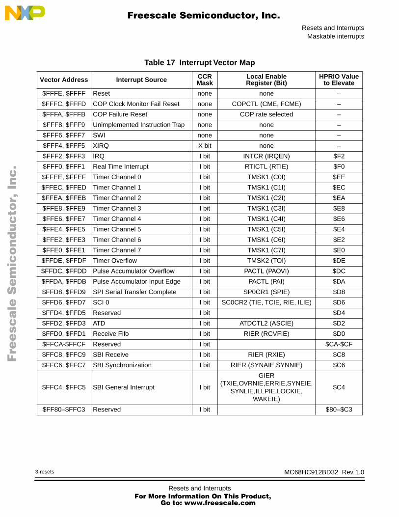
Resets and InterruptsMaskable interrupts
F
ree
sca
le S
em
ico
nd
uc
tor,
I
Freescale Semiconductor, Inc.n
c..
.
Table 17 Interrupt Vector Map
Vector Address Interrupt Source CCR Mask
Local EnableRegister (Bit)
HPRIO Value to Elevate
$FFFE, $FFFF Reset none none –
$FFFC, $FFFD COP Clock Monitor Fail Reset none COPCTL (CME, FCME) –
$FFFA, $FFFB COP Failure Reset none COP rate selected –
$FFF8, $FFF9 Unimplemented Instruction Trap none none –
$FFF6, $FFF7 SWI none none –
$FFF4, $FFF5 XIRQ X bit none –
$FFF2, $FFF3 IRQ I bit INTCR (IRQEN) $F2
$FFF0, $FFF1 Real Time Interrupt I bit RTICTL (RTIE) $F0
$FFEE, $FFEF Timer Channel 0 I bit TMSK1 (C0I) $EE
$FFEC, $FFED Timer Channel 1 I bit TMSK1 (C1I) $EC
$FFEA, $FFEB Timer Channel 2 I bit TMSK1 (C2I) $EA
$FFE8, $FFE9 Timer Channel 3 I bit TMSK1 (C3I) $E8
$FFE6, $FFE7 Timer Channel 4 I bit TMSK1 (C4I) $E6
$FFE4, $FFE5 Timer Channel 5 I bit TMSK1 (C5I) $E4
$FFE2, $FFE3 Timer Channel 6 I bit TMSK1 (C6I) $E2
$FFE0, $FFE1 Timer Channel 7 I bit TMSK1 (C7I) $E0
$FFDE, $FFDF Timer Overflow I bit TMSK2 (TOI) $DE
$FFDC, $FFDD Pulse Accumulator Overflow I bit PACTL (PAOVI) $DC
$FFDA, $FFDB Pulse Accumulator Input Edge I bit PACTL (PAI) $DA
$FFD8, $FFD9 SPI Serial Transfer Complete I bit SP0CR1 (SPIE) $D8
$FFD6, $FFD7 SCI 0 I bit SC0CR2 (TIE, TCIE, RIE, ILIE) $D6
$FFD4, $FFD5 Reserved I bit $D4
$FFD2, $FFD3 ATD I bit ATDCTL2 (ASCIE) $D2
$FFD0, $FFD1 Receive Fifo I bit RIER (RCVFIE) $D0
$FFCA-$FFCF Reserved I bit $CA-$CF
$FFC8, $FFC9 SBI Receive I bit RIER (RXIE) $C8
$FFC6, $FFC7 SBI Synchronization I bit RIER (SYNAIE,SYNNIE) $C6
$FFC4, $FFC5 SBI General Interrupt I bit
GIER(TXIE,OVRNIE,ERRIE,SYNEIE,
SYNLIE,ILLPIE,LOCKIE,WAKEIE)
$C4
$FF80–$FFC3 Reserved I bit $80–$C3
MC68HC912BD32 Rev 1.0
3-resetsResets and Interrupts For More Information On This Product,
Go to: www.freescale.com
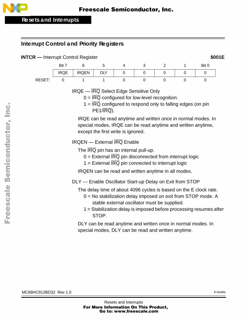
Resets and Interrupts
F
ree
sca
le S
em
ico
nd
uc
tor,
I
Freescale Semiconductor, Inc.n
c..
.
Interrupt Control and Priority Registers
IRQE — IRQ Select Edge Sensitive Only0 = IRQ configured for low-level recognition.1 = IRQ configured to respond only to falling edges (on pin
PE1/IRQ).
IRQE can be read anytime and written once in normal modes. In special modes, IRQE can be read anytime and written anytime, except the first write is ignored.
IRQEN — External IRQ Enable
The IRQ pin has an internal pull-up.0 = External IRQ pin disconnected from interrupt logic1 = External IRQ pin connected to interrupt logic
IRQEN can be read and written anytime in all modes.
DLY — Enable Oscillator Start-up Delay on Exit from STOP
The delay time of about 4096 cycles is based on the E clock rate.0 = No stabilization delay imposed on exit from STOP mode. A
stable external oscillator must be supplied.1 = Stabilization delay is imposed before processing resumes after
STOP.
DLY can be read anytime and written once in normal modes. In special modes, DLY can be read and written anytime.
INTCR — Interrupt Control Register $001E
Bit 7 6 5 4 3 2 1 Bit 0
IRQE IRQEN DLY 0 0 0 0 0
RESET: 0 1 1 0 0 0 0 0
MC68HC912BD32 Rev 1.0
Resets and Interrupts For More Information On This Prod
Go to: www.freescale.com
4-resets
uct,

Resets and InterruptsResets
F
ree
sca
le S
em
ico
nd
uc
tor,
I
Freescale Semiconductor, Inc.n
c..
.
Write only if I mask in CCR = 1 (interrupts inhibited). Read anytime.
To give a maskable interrupt source highest priority, write the low byte of the vector address to the HPRIO register. For example, writing $F0 to HPRIO would assign highest maskable interrupt priority to the real-time interrupt timer ($FFF0). If an unimplemented vector address or a non-I-masked vector address (value higher than $F2) is written, then IRQ will be the default highest priority interrupt.
Resets
There are four possible sources of reset. Power-on reset (POR), and external reset on the RESET pin share the normal reset vector. The computer operating properly (COP) reset and the clock monitor reset each has a vector. Entry into reset is asynchronous and does not require a clock but the MCU cannot sequence out of reset without a system clock.
Power-On Reset A positive transition on VDD causes a power-on reset (POR). An external voltage level detector, or other external reset circuits, are the usual source of reset in a system. The POR circuit only initializes internal circuitry during cold starts and cannot be used to force a reset as system voltage drops.
External Reset The CPU distinguishes between internal and external reset conditions by sensing whether the reset pin rises to a logic one in less than eight E-clock cycles after an internal device releases reset. When a reset condition is sensed, the RESET pin is driven low by an internal device for about 16 E-clock cycles, then released. Eight E-clock cycles later it is sampled. If the pin is still held low, the CPU assumes that an external
HPRIO — Highest Priority I Interrupt $001F
Bit 7 6 5 4 3 2 1 Bit 0
1 1 PSEL5 PSEL4 PSEL3 PSEL2 PSEL1 0
RESET: 1 1 1 1 0 0 1 0
MC68HC912BD32 Rev 1.0
5-resetsResets and Interrupts For More Information On This Product,
Go to: www.freescale.com

Resets and Interrupts
F
ree
sca
le S
em
ico
nd
uc
tor,
I
Freescale Semiconductor, Inc.n
c..
.
reset has occurred. If the pin is high, it indicates that the reset was initiated internally by either the COP system or the clock monitor.
To prevent a COP or clock monitor reset from being detected during an external reset, hold the reset pin low for at least 32 cycles. An external RC power-up delay circuit on the reset pin is not recommended — circuit charge time can cause the MCU to misinterpret the type of reset that has occurred.
COP Reset The MCU includes a computer operating properly (COP) system to help protect against software failures. When COP is enabled, software must write $55 and $AA (in this order) to the COPRST register in order to keep a watchdog timer from timing out. Other instructions may be executed between these writes. A write of any value other than $55 or $AA or software failing to execute the sequence properly causes a COP reset to occur.
Clock Monitor Reset
If clock frequency falls below a predetermined limit when the clock monitor is enabled, a reset occurs.
Effects of Reset
When a reset occurs, MCU registers and control bits are changed to known start-up states, as follows.
Operating Mode and Memory Map
Operating mode and default memory mapping are determined by the states of the BKGD, MODA, and MODB pins during reset. The SMODN, MODA, and MODB bits in the MODE register reflect the status of the mode-select inputs at the rising edge of reset. Operating mode and default maps can subsequently be changed according to strictly defined rules.
MC68HC912BD32 Rev 1.0
Resets and Interrupts For More Information On This Prod
Go to: www.freescale.com
6-resets
uct,

Resets and InterruptsEffects of Reset
MC68HC912BD32 Rev 1.0
F
ree
sca
le S
em
ico
nd
uc
tor,
I
Freescale Semiconductor, Inc.n
c..
.
7-resets
Clock and Watchdog Control Logic
The COP watchdog system is enabled, with the CR [2:0] bits set for the shortest duration time-out. The clock monitor is disabled. The RTIF flag is cleared and automatic hardware interrupts are masked. The rate control bits are cleared, and must be initialized before the RTI system is used. The DLY control bit is set to specify an oscillator start-up delay upon recovery from STOP mode.
Interrupts PSEL is initialized in the HPRIO register with the value $F2, causing the external IRQ pin to have the highest I-bit interrupt priority. The IRQ pin is configured for level-sensitive operation (for wired-OR systems). However, the interrupt mask bits in the CPU12 CCR are set to mask X and I related interrupt requests.
Parallel I/O If the MCU comes out of reset in an expanded mode, port A and port B are used for the multiplexed address/data bus and port E pins are normally used to control the external bus (operation of port E pins can be affected by the PEAR register). If the MCU comes out of reset in a single-chip mode, all ports are configured as general-purpose high-impedance inputs. Port S, port T, port DLC, port P, and port AD are all configured as general-purpose inputs.
Central Processing Unit
After reset, the CPU fetches a vector from the appropriate address, then begins executing instructions. The stack pointer and other CPU registers are indeterminate immediately after reset. The CCR X and I interrupt mask bits are set to mask any interrupt requests. The S bit is also set to inhibit the STOP instruction.
Memory After reset, the internal register block is located at $0000–$01FF, the register-following space is at $0200–$03FF, and RAM is at $0800–$0BFF. EEPROM is located at $0D00–$0FFF. Flash EEPROM is located at $8000–$FFFF in single-chip modes and at $0000–$7FFF (but disabled) in expanded modes.
Other Resources The timer, serial communications interface (SCI), serial peripheral interface (SPI), Byteflight™, pulse-width modulator (PWM), and analog-to-digital converter (ATD) are off after reset.
Resets and Interrupts For More Information On This Product,
Go to: www.freescale.com

Resets and Interrupts
F
ree
sca
le S
em
ico
nd
uc
tor,
I
Freescale Semiconductor, Inc.n
c..
.
Register Stacking
Once enabled, an interrupt request can be recognized at any time after the I bit in the CCR is cleared. When an interrupt service request is recognized, the CPU responds at the completion of the instruction being executed. Interrupt latency varies according to the number of cycles required to complete the instruction. Some of the longer instructions can be interrupted and will resume normally after servicing the interrupt.
When the CPU begins to service an interrupt, the instruction queue is cleared, the return address is calculated, and then it and the contents of the CPU registers are stacked as shown in Table 18.
After the CCR is stacked, the I bit (and the X bit, if an XIRQ interrupt service request is pending) is set to prevent other interrupts from disrupting the interrupt service routine. The interrupt vector for the highest priority source that was pending at the beginning of the interrupt sequence is fetched, and execution continues at the referenced location. At the end of the interrupt service routine, an RTI instruction restores the content of all registers from information on the stack, and normal program execution resumes. If another interrupt is pending at the end of an interrupt service routine, the register unstacking and restacking is bypassed and the vector of the pending interrupt is fetched.
Table 18 Stacking Order on Entry to Interrupts
Memory Location CPU Registers
SP – 2 RTNH : RTNL
SP – 4 YH : YL
SP – 6 XH : XL
SP – 8 B : A
SP – 9 CCR
MC68HC912BD32 Rev 1.0
Resets and Interrupts For More Information On This Prod
Go to: www.freescale.com
8-resets
uct,
F
ree
sca
le S
em
ico
nd
uc
tor,
IFreescale Semiconductor, Inc.
nc
...
ClocksClocks
Contents
Introduction . . . . . . . . . . . . . . . . . . . . . . . . . . . . . . . . . . . . . . . . . . . . . 97Clock Selection and Generation . . . . . . . . . . . . . . . . . . . . . . . . . . . . . 97Slow Mode Divider . . . . . . . . . . . . . . . . . . . . . . . . . . . . . . . . . . . . . . 100CGM Register Description . . . . . . . . . . . . . . . . . . . . . . . . . . . . . . . . 100Clock Functions. . . . . . . . . . . . . . . . . . . . . . . . . . . . . . . . . . . . . . . . . 101Computer Operating Properly (COP) . . . . . . . . . . . . . . . . . . . . . . . . 101Real-Time Interrupt . . . . . . . . . . . . . . . . . . . . . . . . . . . . . . . . . . . . . . 102Clock Monitor . . . . . . . . . . . . . . . . . . . . . . . . . . . . . . . . . . . . . . . . . . 102Clock Function Registers . . . . . . . . . . . . . . . . . . . . . . . . . . . . . . . . . 103Clock Divider Chains. . . . . . . . . . . . . . . . . . . . . . . . . . . . . . . . . . . . . 107
Introduction
The clock generation module (CGM) generates the system clocks and generates and controls the timing of the reset and power-on reset logic. The clock generation module is composed of:
• clock selection and generation circuitry
• slow mode clock divider
• reset and stop generation timing and control
Clock Selection and Generation
The clock generation module generates the P clock, the E clock, and four T clocks. The P clock and E clock are used by all device modules except the CPU. The T clocks are used by the CPU.
MC68HC912BD32 Rev 1.0
1-clockClocks For More Information On This Product,
Go to: www.freescale.com

Clocks
F
ree
sca
le S
em
ico
nd
uc
tor,
I
Freescale Semiconductor, Inc.n
c..
.
Figure 9 Clock Selection
Figure 10 shows clock timing relationships while in normal run modes.
Figure 10 Internal Clock Relationships in Normal Run Modes
EXTAL
XTALE CLOCK
P CLOCK
T CLOCKT CLOCKGENERATOR TO CPU
SLOW MODECLOCK DIVIDER WAIT
SLOW E CLOCKOSCILLATOR
÷ 2
E AND P CLOCKGENERATOR TO TIME CLOCK (GBT)
P CLOCK (GBT)
TO BUSES, BDM,SPI, SCI, ATD, RTI,COP, PWM, FEE,EE, RAM, SIBUS12
SLOW P CLOCK
OUT
÷ 2
OSCILLATORAND
CLOCKGENERATOR
DIVBYP
TO SIBUS12
T1 CLOCK
T2 CLOCK
T3 CLOCK
T4 CLOCK
E CLOCK
P CLOCK
OSCILLATOR
MC68HC912BD32 Rev 1.0
Clocks For More Information On This Prod
Go to: www.freescale.com
2-clock
uct,
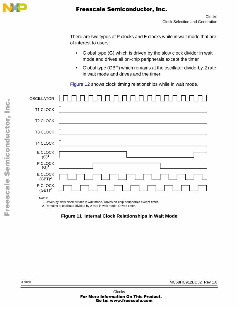
ClocksClock Selection and Generation
F
ree
sca
le S
em
ico
nd
uc
tor,
I
Freescale Semiconductor, Inc.n
c..
.
There are two types of P clocks and E clocks while in wait mode that are of interest to users:
• Global type (G) which is driven by the slow clock divider in wait mode and drives all on-chip peripherals except the timer
• Global type (GBT) which remains at the oscillator divide-by-2 rate in wait mode and drives and the timer.
Figure 12 shows clock timing relationships while in wait mode.
Figure 11 Internal Clock Relationships in Wait Mode
E CLOCK
P CLOCK
OSCILLATOR
T1 CLOCK
T2 CLOCK
T3 CLOCK
T4 CLOCK
E CLOCK
P CLOCK
1. Driven by slow clock divider in wait mode. Drives on-chip peripherals except timer.2. Remains at oscillator divided by 2 rate in wait mode. Drives timer.
Notes:
(G)1
(G)1
(GBT)2
(GBT)2
MC68HC912BD32 Rev 1.0
3-clockClocks For More Information On This Product,
Go to: www.freescale.com
Clocks
F
ree
sca
le S
em
ico
nd
uc
tor,
I
Freescale Semiconductor, Inc.n
c..
.
Slow Mode Divider
The slow mode divider is included to deliver a variable bus frequency to the MCU in wait mode. The bus clocks are derived from the constant P clock. The slow clock counter divides the P clock and E clock frequency in powers of 2, up to 128. When the slow control register is cleared or the part is not in wait mode, the slow mode divider is off and the bus clocks frequency is not changed.
NOTE: The clock monitor is clocked by the system clock (oscillator) reference; the slow mode divider allows operation of the MCU at clock periods longer than the clock monitor trigger time.
CGM Register Description
SLDV2–SLDV0 — Slow Mode Divisor Selector Bits
The value 2 raised to the power indicated by these three bits, produce the slow mode frequency divider. The range of the divider is 2 to 128 by steps of power of 2. When the bits are clear, the divider is bypassed. Figure 19 shows the divider for all bit conditions and the resulting bus rate for three example oscillator frequencies.
SLOW — Slow Mode Divider Register $00E0
Bit 7 6 5 4 3 2 1 Bit 0
0 0 0 0 0 SLDV2 SLDV1 SLDV0
RESET: 0 0 0 0 0 0 0 0
MC68HC912BD32 Rev 1.0
Clocks For More Information On This Prod
Go to: www.freescale.com
4-clock
uct,
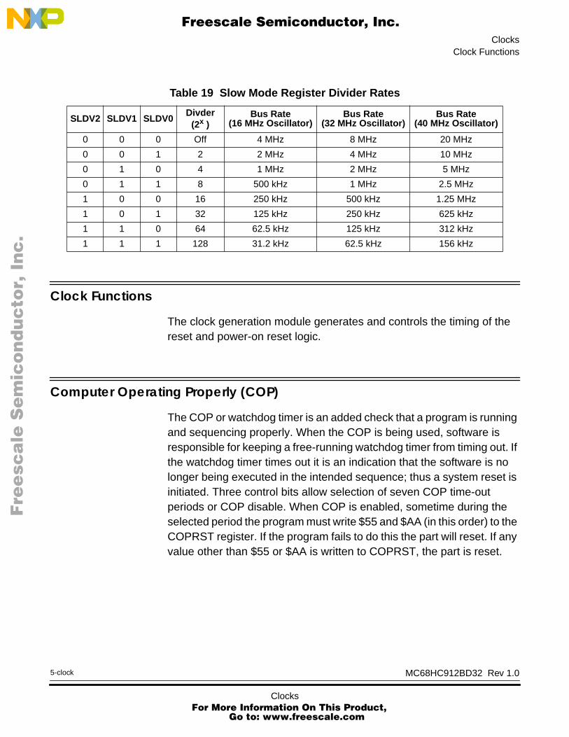
ClocksClock Functions
F
ree
sca
le S
em
ico
nd
uc
tor,
I
Freescale Semiconductor, Inc.n
c..
.
Clock Functions
The clock generation module generates and controls the timing of the reset and power-on reset logic.
Computer Operating Properly (COP)
The COP or watchdog timer is an added check that a program is running and sequencing properly. When the COP is being used, software is responsible for keeping a free-running watchdog timer from timing out. If the watchdog timer times out it is an indication that the software is no longer being executed in the intended sequence; thus a system reset is initiated. Three control bits allow selection of seven COP time-out periods or COP disable. When COP is enabled, sometime during the selected period the program must write $55 and $AA (in this order) to the COPRST register. If the program fails to do this the part will reset. If any value other than $55 or $AA is written to COPRST, the part is reset.
Table 19 Slow Mode Register Divider Rates
SLDV2 SLDV1 SLDV0Divder
(2x )Bus Rate
(16 MHz Oscillator)Bus Rate
(32 MHz Oscillator)Bus Rate
(40 MHz Oscillator)
0 0 0 Off 4 MHz 8 MHz 20 MHz
0 0 1 2 2 MHz 4 MHz 10 MHz
0 1 0 4 1 MHz 2 MHz 5 MHz
0 1 1 8 500 kHz 1 MHz 2.5 MHz
1 0 0 16 250 kHz 500 kHz 1.25 MHz
1 0 1 32 125 kHz 250 kHz 625 kHz
1 1 0 64 62.5 kHz 125 kHz 312 kHz
1 1 1 128 31.2 kHz 62.5 kHz 156 kHz
MC68HC912BD32 Rev 1.0
5-clockClocks For More Information On This Product,
Go to: www.freescale.com

Clocks
F
ree
sca
le S
em
ico
nd
uc
tor,
I
Freescale Semiconductor, Inc.n
c..
.
Real-Time Interrupt
There is a real-time (periodic) interrupt available to the user. This interrupt will occur at one of seven selected rates. An interrupt flag and an interrupt enable bit are associated with this function. There are three bits for the rate select.
Clock Monitor
The clock monitor circuit is based on an internal resistor-capacitor (RC) time delay. If no MCU clock edges are detected within this RC time delay, the clock monitor can optionally generate a system reset. The clock monitor function is enabled/disabled by the CME control bit in the COPCTL register. This time-out is based on an RC delay so that the clock monitor can operate without any MCU clocks.
Clock monitor time-outs are shown in Table 20.
Table 20 Clock Monitor Time-Outs
Supply Range
5V +/− 5% 2-20 µS
MC68HC912BD32 Rev 1.0
Clocks For More Information On This Prod
Go to: www.freescale.com
6-clock
uct,

ClocksClock Function Registers
MC68HC912BD32 Rev 1.0
F
ree
sca
le S
em
ico
nd
uc
tor,
I
Freescale Semiconductor, Inc.n
c..
.
7-clock
Clock Function Registers
All register addresses shown reflect the reset state. Registers may be mapped to any 2-Kbyte space.
RTIE — Real-Time Interrupt Enable
Read and write anytime.0 = Interrupt requests from RTI are disabled.1 = Interrupt will be requested whenever RTIF is set.
RSWAI — RTI and COP Stop While in Wait
Write once in normal modes, anytime in special modes. Read anytime.
0 = Allows the RTI and COP to continue running in wait.1 = Disables both the RTI and COP whenever the part goes into
wait.
RSBCK — RTI and COP Stop While in Background Debug Mode
Write once in normal modes, anytime in special modes. Read anytime.
0 = Allows the RTI and COP to continue running while in background mode.
1 = Disables both the RTI and COP whenever the part is in background mode. This is useful for emulation.
RTBYP — Real-Time Interrupt Divider Chain Bypass
Write not allowed in normal modes, anytime in special modes. Read anytime.
0 = Divider chain functions normally.1 = Divider chain is bypassed, allows faster testing (the divider
chain is normally P divided by 213, when bypassed becomes P divided by 4).
RTICTL — Real-Time Interrupt Control Register $0014
Bit 7 6 5 4 3 2 1 Bit 0
RTIE RSWAI RSBCK 0 RTBYP RTR2 RTR1 RTR0
RESET: 0 0 0 0 0 0 0 0
Clocks For More Information On This Product,
Go to: www.freescale.com

Clocks
F
ree
sca
le S
em
ico
nd
uc
tor,
I
Freescale Semiconductor, Inc.n
c..
.
RTR2, RTR1, RTR0 — Real-Time Interrupt Rate Select
Read and write anytime.
Rate select for real-time interrupt. The clock used for this module is the E clock.
RTIF — Real-Time Interrupt Flag
This bit is cleared automatically by a write to this register with this bit set.
0 = Time-out has not yet occurred.1 = Set when the time-out period is met.
CME — Clock Monitor Enable
Read and write anytime.
If FCME is set, this bit has no meaning nor effect.
Table 21 Real Time Interrupt Rates
RTR2 RTR1 RTR0 Divide E By:
Time-Out PeriodE = 4.0 MHz
Time-Out PeriodE = 8.0 MHz
Time-Out PeriodE = 10.0 MHz
0 0 0 OFF OFF OFF OFF
0 0 1 213 2.048 ms 1.024 ms 0.819 ms
0 1 0 214 4.096 ms 2.048 ms 1.638 ms
0 1 1 215 8.192 ms 4.096 ms 3.277 ms
1 0 0 216 16.384 ms 8.192 ms 6.554 ms
1 0 1 217 32.768 ms 16.384 ms 13.107 ms
1 1 0 218 65.536 ms 32.768 ms 26.214 ms
1 1 1 219 131.072 ms 65.536 ms 52.429 ms
RTIFLG — Real-Time Interrupt Flag Register $0015
Bit 7 6 5 4 3 2 1 Bit 0
RTIF 0 0 0 0 0 0 0
RESET: 0 0 0 0 0 0 0 0
COPCTL — COP Control Register $0016
Bit 7 6 5 4 3 2 1 Bit 0
CME FCME FCM FCOP DISR CR2 CR1 CR0
RESET: 0 0 0 0 0 0 0 1 Normal
RESET: 0 0 0 0 1 0 0 1 Special
MC68HC912BD32 Rev 1.0
Clocks For More Information On This Prod
Go to: www.freescale.com
8-clock
uct,

ClocksClock Function Registers
MC68HC912BD32 Rev 1.0
F
ree
sca
le S
em
ico
nd
uc
tor,
I
Freescale Semiconductor, Inc.n
c..
.
9-clock
0 = Clock monitor is disabled. Slow clocks and stop instruction may be used.
1 = Slow or stopped clocks (including the stop instruction) will cause a clock reset sequence.
FCME — Force Clock Monitor Enable
Write once in normal modes, anytime in special modes. Read anytime.
In normal modes, when this bit is set, the clock monitor function cannot be disabled until a reset occurs.
0 = Clock monitor follows the state of the CME bit.1 = Slow or stopped clocks will cause a clock reset sequence.
In order to use both STOP and clock monitor, the CME bit should be cleared prior to executing a STOP instruction and set after recovery from STOP. If you plan on using STOP always keep FCME = 0.
FCM — Force Clock Monitor Reset
Writes are not allowed in normal modes, anytime in special modes. Read anytime.
If DISR is set, this bit has no effect.0 = Normal operation.1 = Force a clock monitor reset (if clock monitor is enabled).
FCOP — Force COP Watchdog Reset
Writes are not allowed in normal modes; can be written anytime in special modes. Read anytime.
If DISR is set, this bit has no effect.0 = Normal operation.1 = Force a COP reset (if COP is enabled).
DISR — Disable Resets from COP Watchdog and Clock Monitor
Writes are not allowed in normal modes, anytime in special modes. Read anytime.
0 = Normal operation.1 = Regardless of other control bit states, COP and clock monitor
will not generate a system reset.
Clocks For More Information On This Product,
Go to: www.freescale.com

Clocks
F
ree
sca
le S
em
ico
nd
uc
tor,
I
Freescale Semiconductor, Inc.n
c..
.
CR2, CR1, CR0 — COP Watchdog Timer Rate Select Bits
The COP system is driven by a constant frequency of E/213. (RTBYP in the RTICTL register allows all but two stages of this divider to be bypassed for testing in special modes only.) These bits specify an additional division factor to arrive at the COP time-out rate (the clock used for this module is the E clock).
Write once in normal modes, anytime in special modes. Read anytime.
Always reads $00.
Writing $55 to this address is the first step of the COP watchdog sequence.
Writing $AA to this address is the second step of the COP watchdog sequence. Other instructions may be executed between these writes but both must be completed in the correct order prior to time-out to avoid a watchdog reset. Writing anything other than $55 or $AA causes a COP reset to occur.
Table 22 COP Watchdog Rates (RTBYP = 0)
CR2 CR1 CR0 Divide E By:
At E = 4.0 MHzTime-Out
–0 to +2.048 s
At E = 8.0 MHzTime-Out
–0 to +1.024 s
At E = 10.0 MHzTime-Out
–0 to +838.861 ms
0 0 0 OFF OFF OFF OFF
0 0 1 213 2.048 ms 1.024 ms 0.819 ms
0 1 0 215 8.192 ms 4.096 ms 3.277 ms
0 1 1 217 32.768 ms 16.384 ms 13.107 ms
1 0 0 219 131.072 ms 65.536 ms 52.429 ms
1 0 1 221 524.288 ms 262.144 ms 209.715 ms
1 1 0 222 1.048 s 524.288 ms 419.430 ms
1 1 1 223 2.097 s 1.048576 s 838.861 ms
COPRST — Arm/Reset COP Timer Register $0017
Bit 7 6 5 4 3 2 1 Bit 0
Bit 7 6 5 4 3 2 1 Bit 0
RESET: 0 0 0 0 0 0 0 0
MC68HC912BD32 Rev 1.0
Clocks For More Information On This Prod
Go to: www.freescale.com
10-clock
uct,

ClocksClock Divider Chains
MC68HC912BD32 Rev 1.0
F
ree
sca
le S
em
ico
nd
uc
tor,
I
Freescale Semiconductor, Inc.n
c..
.
11-clock
Clock Divider Chains
Figure 12, Figure 13, and Figure 14 summarize the clock divider chains for the various peripherals on the MC68HC912BD32.
Figure 12 Clock Chain for SCI, RTI, COP
PC
LK
SC0BDMODULUS DIVIDER:
÷ 1, 2, 3, 4, 5, 6, ..., 8190, 8191
SCI0RECEIVE
BAUD RATE ((16x)
SCI0TRANSMIT
BAUD RATE (1x)
BITS: RTR2, RTR1, RTR0
TO RTI
BITS: CR2, CR1, CR0
TO COP
÷ 24
0:0:0
0:0:1
0:1:0
0:1:1
1:0:0
1:0:1
1:1:0
1:1:1
÷ 2
÷ 2
÷ 2
÷ 2
÷ 2
÷ 2
0:0:0
0:0:1
0:1:0
0:1:1
1:0:0
1:0:1
1:1:0
1:1:1
÷ 4
÷ 4
÷ 4
÷ 2
÷ 4
÷ 2
REGISTER: COPCTLREGISTER: RTICTL
÷ 211÷ 22
BIT: RTBYPREGISTER: RTICTL
Clocks For More Information On This Product,
Go to: www.freescale.com
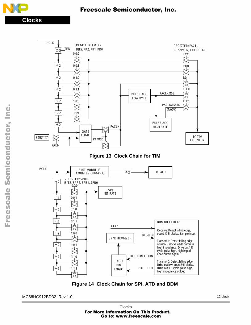
Clocks
F
ree
sca
le S
em
ico
nd
uc
tor,
I
Freescale Semiconductor, Inc.n
c..
.
Figure 13 Clock Chain for TIM
Figure 14 Clock Chain for SPI, ATD and BDM
BITS: PR2, PR1, PR0
PCLK
1:0:0
1:0:1
1:1:0
1:1:1
TO TIM COUNTER
PORT T7 PAMOD
PACLK
PULSE ACCLOW BYTE
PACLK/256
PULSE ACCHIGH BYTE
PACLK/65536(PAOV)
GATELOGIC
BITS: PAEN, CLK1, CLK00:x:x
TEN
PAEN
0:0:0
0:0:1
0:1:0
0:1:1
1:0:0
1:0:1
÷ 2
÷ 2
÷ 2
÷ 2
÷ 2
÷ 2
REGISTER: PACTLREGISTER: TMSK2
PCLK
BITS: SPR2, SPR1, SPR0
SPI BIT RATE
5-BIT MODULUS COUNTER (PR0-PR4) TO ATD
ECLK
BKGD
BDM BIT CLOCK:
Receive: Detect falling edge, count 12 E clocks, Sample input
Transmit 1: Detect falling edge, count 6 E clocks while output is high impedance, Drive out 1 E cycle pulse high, high imped-ance output again
Transmit 0: Detect falling edge, Drive out low, count 9 E clocks, Drive out 1 E cycle pulse high, high impedance output
PIN
SYNCHRONIZER
LOGIC
BKGD IN
BKGD OUT
BKGD DIRECTION
÷ 2
0:0:0
0:0:1
0:1:0
0:1:1
1:0:0
1:0:1
1:1:0
1:1:1
÷ 2
÷ 2
÷ 2
÷ 2
÷ 2
÷ 2
÷ 2
÷ 2REGISTER: SP0BR
MC68HC912BD32 Rev 1.0
Clocks For More Information On This Prod
Go to: www.freescale.com
12-clock
uct,

F
ree
sca
le S
em
ico
nd
uc
tor,
IFreescale Semiconductor, Inc.
nc
...
Pulse Width ModulatorPulse Width Modulator
Contents
Introduction . . . . . . . . . . . . . . . . . . . . . . . . . . . . . . . . . . . . . . . . . . . . 109PWM Register Description . . . . . . . . . . . . . . . . . . . . . . . . . . . . . . . . 114PWM Boundary Cases . . . . . . . . . . . . . . . . . . . . . . . . . . . . . . . . . . . 125
Introduction
The pulse-width modulator (PWM) subsystem provides four independent 8-bit PWM waveforms or two 16-bit PWM waveforms or a combination of one 16-bit and two 8-bit PWM waveforms. Each waveform channel has a programmable period and a programmable duty-cycle as well as a dedicated counter. A flexible clock select scheme allows four different clock sources to be used with the counters. Each of the modulators can create independent, continuous waveforms with software-selectable duty rates from 0 percent to 100 percent. The PWM outputs can be programmed as left-aligned outputs or center-aligned outputs.
The four PWM channel outputs share general-purpose port P pins. Enabling PWM pins takes precedence over the general-purpose port. When PWM are not in use, the port pins may be used for discrete input/output.
The period and duty registers are double buffered so that if they change while the channel is enabled, the change will not take effect until the counter reaches zero or the channel is disabled and then re-enabled. If the channel is not enabled then writes to the period and/or duty register will go only to the shadow latches. When the channel is enabled (PWENx) is written from 0 to 1) the counter direction is set to UP and the Shadow to Register transfer for PWPERx and PWDTYx is done.
MC68HC912BD32 Rev 1.0
1-pwmPulse Width Modulator For More Information On This Product,
Go to: www.freescale.com

Pulse Width Modulator
F
ree
sca
le S
em
ico
nd
uc
tor,
I
Freescale Semiconductor, Inc.n
c..
.
For Center Aligned mode two additional initialization operations occur: the PWM counter is reset to $00 and a decision for the PWM output value takes place. In this way the output of the PWM will always be; the old waveform, or the new waveform and not some variation of the two.
The pulse modulated signal becomes available at port P output when the PWM channel clock source begins its next cycle.
A change in duty or period can be forced into immediate effect by writing the new value to the duty and/or period registers and then writing to the counter. This causes the counter to reset and the new duty and/or period values to be latched (this may cause a truncated PWM period). In addition, since the counter is readable it is possible to know where the count is with respect to the duty value and software can be used to make adjustments by turning the enable bit off and on (only in Left Aligned output mode).
MC68HC912BD32 Rev 1.0
Pulse Width Modulator For More Information On This Prod
Go to: www.freescale.com
2-pwm
uct,

Pulse Width ModulatorIntroduction
F
ree
sca
le S
em
ico
nd
uc
tor,
I
Freescale Semiconductor, Inc.n
c..
.
Figure 15 Block Diagram of PWM Left-Aligned Output Channel
(duty cycle)
Clock Source(E or Scaled E)
reset
S
R
Q
Q
MUX
PPOLx
From Port PData Register
PWENx
PWDTY
PWPER
(clock edge sync)
To PinDriver
PWCNTxGATE
8-bit Compare =
PWDTYx
(period)
8-bit Compare =
PWPERx
MUX
CENTR=0
up/down
PPOL=0
PPOL=1
Sync
PW
Mx_
cloc
k
MC68HC912BD32 Rev 1.0
3-pwmPulse Width Modulator For More Information On This Product,
Go to: www.freescale.com

Pulse Width Modulator
F
ree
sca
le S
em
ico
nd
uc
tor,
I
Freescale Semiconductor, Inc.n
c..
.
Figure 16 Block Diagram of PWM Center-Aligned Output Channel
(duty cycle)
Clock Source(E or Scaled E)
up/down
T Q
Q
MUX
PPOLx
From Port PData Register
PWENx
PWDTY
Period = PWPER*2
(clock edge sync)
To PinDriver
PWCNTxGATE
8-bit Compare =
PWDTYx
(period)
8-bit Compare =
PWPERx
MUX
CENTR=1
reset
PPOL= 1 0
PPOL= 0 1
Sync
PW
Mx_
cloc
k
PWDTY(PWPER–PWDTY)*2
MC68HC912BD32 Rev 1.0
Pulse Width Modulator For More Information On This Prod
Go to: www.freescale.com
4-pwm
uct,

Pulse Width ModulatorIntroduction
F
ree
sca
le S
em
ico
nd
uc
tor,
I
Freescale Semiconductor, Inc.n
c..
.
Figure 17 PWM Clock Sources
24
816
3264
128
PC
KB
2P
CK
B1
PC
KB
0
PC
KA
2P
CK
A1
PC
KA
0
PCLK0
Clock toPWM
loadPWSCNT0
DIV 28-bit Scale Reg
PWSCAL0
8-bit Down Counter
Clock A
Clo
ck S
0
Clock A/2, A/4, A/6,....A/512
PRESCALE SCALE
PW
PR
ES
Pre
scal
er T
aps
Div
ide
By:
PS
BC
KLI
MB
DM
E C
lock
channel 0
MUX
PCLK1
Clock toPWMchannel 1
MUX
MUX
PCLK2
Clock toPWM
loadPWSCNT1
DIV 28-bit Scale Reg
PWSCAL1
8-bit Down Counter
Clock B
Clo
ck S
1
Clock B/2, B/4, B/6,....B/512
channel 2
MUX
PCLK3
Clock toPWMchannel 3
MUX
MUX
MC68HC912BD32 Rev 1.0
5-pwmPulse Width Modulator For More Information On This Product,
Go to: www.freescale.com

Pulse Width Modulator
F
ree
sca
le S
em
ico
nd
uc
tor,
I
Freescale Semiconductor, Inc.n
c..
.
PWM Register Description
Read and write anytime.
CON23 — Concatenate PWM Channels 2 and 3
When concatenated, channel 2 becomes the high-order byte and channel 3 becomes the low-order byte. Channel 2 output pin is used as the output for this 16-bit PWM (bit 2 of port P). Channel 3 clock-select control bits determines the clock source.
0 = Channels 2 and 3 are separate 8-bit PWMs.1 = Channels 2 and 3 are concatenated to create one 16-bit PWM
channel.
CON01 — Concatenate PWM Channels 0 and 1
When concatenated, channel 0 becomes the high-order byte and channel 1 becomes the low-order byte. Channel 0 output pin is used as the output for this 16-bit PWM (bit 0 of port P). Channel 1 clock-select control bits determines the clock source.
0 = Channels 0 and 1 are separate 8-bit PWMs.1 = Channels 0 and 1 are concatenated to create one 16-bit PWM
channel.
NOTE: These bits should be changed only when both corresponding channels are disabled. For Left Aligned output mode operation when changing these bits the user should write to the associated PWM counters as the LAST operation before enabling (setting PWENx = q) the channel(s).
PCKA2–PCKA0 — Prescaler for Clock A
Clock A is one of two clock sources which may be used for channels 0 and 1. These three bits determine the rate of clock A, as shown in Table 23.
PWCLK — PWM Clock Select Register with Concatenate Bits $0040
Bit 7 6 5 4 3 2 1 Bit 0
CON23 CON01 PCKA2 PCKA1 PCKA0 PCKB2 PCKB1 PCKB0
RESET: 0 0 0 0 0 0 0 0
MC68HC912BD32 Rev 1.0
Pulse Width Modulator For More Information On This Prod
Go to: www.freescale.com
6-pwm
uct,

Pulse Width ModulatorPWM Register Description
MC68HC912BD32 Rev 1.0
F
ree
sca
le S
em
ico
nd
uc
tor,
I
Freescale Semiconductor, Inc.n
c..
.
7-pwm
PCKB2–PCKB0 — Prescaler for Clock B
Clock B is one of two clock sources which may be used for channels 2 and 3. These three bits determine the rate of clock B, as shown in Table 23.
Read and write anytime.
PCLK3 — PWM Channel 3 Clock Select0 = Clock B is the clock source for channel 3.1 = Clock S1 is the clock source for channel 3.
PCLK2 — PWM Channel 2 Clock Select0 = Clock B is the clock source for channel 2.1 = Clock S1 is the clock source for channel 2.
PCLK1 — PWM Channel 1 Clock Select0 = Clock A is the clock source for channel 1.1 = Clock S0 is the clock source for channel 1.
PCLK0 — PWM Channel 0 Clock Select0 = Clock A is the clock source for channel 0.1 = Clock S0 is the clock source for channel 0.
Table 23 Clock A and Clock B Prescaler
PCKA2(PCKB2)
PCKA1(PCKB1)
PCKA0(PCKB0)
Value ofClock A (B)
0 0 0 E
0 0 1 E/ 20 1 0 E/4
0 1 1 E/ 81 0 0 E/16
1 0 1 E/ 32
1 1 0 E/ 64
1 1 1 E/ 128
PWPOL— PWM Clock Select and Polarity $0041
Bit 7 6 5 4 3 2 1 Bit 0
PCLK3 PCLK2 PCLK1 PCLK0 PPOL3 PPOL2 PPOL1 PPOL0
RESET: 0 0 0 0 0 0 0 0
Pulse Width Modulator For More Information On This Product,
Go to: www.freescale.com

Pulse Width Modulator
F
ree
sca
le S
em
ico
nd
uc
tor,
I
Freescale Semiconductor, Inc.n
c..
.
PPOL3 — PWM Channel 3 Polarity0 = Channel 3 output is low at the beginning of the period; high
when the duty count is reached.1 = Channel 3 output is high at the beginning of the period; low
when the duty count is reached.
PPOL2 — PWM Channel 2 Polarity0 = Channel 2 output is low at the beginning of the period; high
when the duty count is reached.1 = Channel 2 output is high at the beginning of the period; low
when the duty count is reached.
PPOL1 — PWM Channel 1 Polarity0 = Channel 1 output is low at the beginning of the period; high
when the duty count is reached.1 = Channel 1 output is high at the beginning of the period; low
when the duty count is reached.
PPOL0 — PWM Channel 0 Polarity0 = Channel 0 output is low at the beginning of the period; high
when the duty count is reached.1 = Channel 0 output is high at the beginning of the period; low
when the duty count is reached.
NOTE: Register bits PCLK0 to PCLK3 may be written anytime. If a clock select is changed while a PWM signal is being generated, a truncated or stretched pulse may occur during transition.
NOTE: Depending on the polarity bit, the duty registers may contain the count of either the high time or the low time. If the polarity bit is one, the output starts high and then goes low when the duty count is reached, so the duty registers contain a count of the high time. If the polarity bit is zero, the output starts low and then goes high when the duty count is reached, so the duty registers contain a count of the low time.
MC68HC912BD32 Rev 1.0
Pulse Width Modulator For More Information On This Prod
Go to: www.freescale.com
8-pwm
uct,
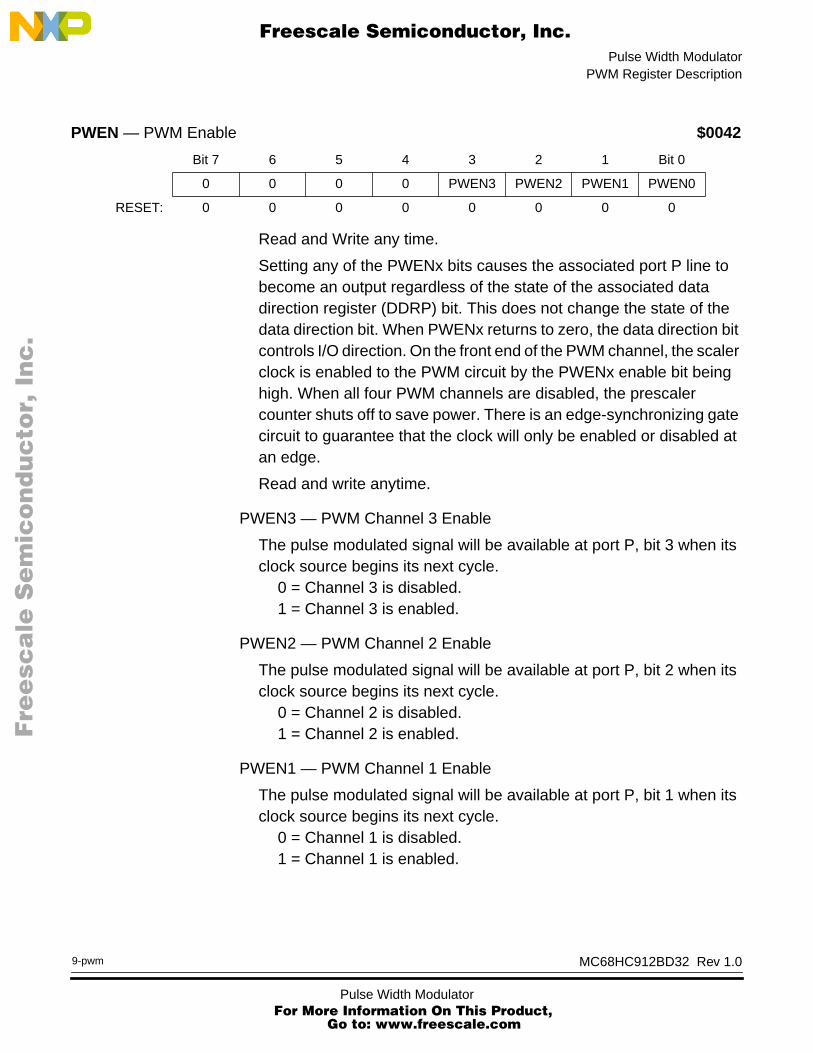
Pulse Width ModulatorPWM Register Description
MC68HC912BD32 Rev 1.0
F
ree
sca
le S
em
ico
nd
uc
tor,
I
Freescale Semiconductor, Inc.n
c..
.
9-pwm
Read and Write any time.
Setting any of the PWENx bits causes the associated port P line to become an output regardless of the state of the associated data direction register (DDRP) bit. This does not change the state of the data direction bit. When PWENx returns to zero, the data direction bit controls I/O direction. On the front end of the PWM channel, the scaler clock is enabled to the PWM circuit by the PWENx enable bit being high. When all four PWM channels are disabled, the prescaler counter shuts off to save power. There is an edge-synchronizing gate circuit to guarantee that the clock will only be enabled or disabled at an edge.
Read and write anytime.
PWEN3 — PWM Channel 3 Enable
The pulse modulated signal will be available at port P, bit 3 when its clock source begins its next cycle.
0 = Channel 3 is disabled.1 = Channel 3 is enabled.
PWEN2 — PWM Channel 2 Enable
The pulse modulated signal will be available at port P, bit 2 when its clock source begins its next cycle.
0 = Channel 2 is disabled.1 = Channel 2 is enabled.
PWEN1 — PWM Channel 1 Enable
The pulse modulated signal will be available at port P, bit 1 when its clock source begins its next cycle.
0 = Channel 1 is disabled.1 = Channel 1 is enabled.
PWEN — PWM Enable $0042
Bit 7 6 5 4 3 2 1 Bit 0
0 0 0 0 PWEN3 PWEN2 PWEN1 PWEN0
RESET: 0 0 0 0 0 0 0 0
Pulse Width Modulator For More Information On This Product,
Go to: www.freescale.com

Pulse Width Modulator
F
ree
sca
le S
em
ico
nd
uc
tor,
I
Freescale Semiconductor, Inc.n
c..
.
PWEN0 — PWM Channel 0 Enable
The pulse modulated signal will be available at port P, bit 0 when its clock source begins its next cycle.
0 = Channel 0 is disabled.1 = Channel 0 is enabled.
PWPRES is a free running 7-bit counter. Read anytime. Write only in Special mode (SMOD = 1).
Read and write anytime. A write will cause the scaler counter PWSCNT0 to load the PWSCAL0 value unless in Special mode with DISCAL =1 in the PWTST register.
PWM channels 0 and 1 can select clock S0 (scaled) as its input clock by setting the control bit PCLK0 and PCLK1 respectively. Clock S0 is generated by dividing clock A by the value in the PWSCAL0 register and dividing again by two. When PWSCAL0 = $FF, clock A is divided by 256 then divided by two to generate clock S0. In Special Mode when DISCAL = 1, writes to PWSCAL0 does not load Scale-Counter 0 (PWSCNT0).
PWPRES— PWM Prescale Counter $0043
Bit 7 6 5 4 3 2 1 Bit 0
0 Bit 6 5 4 3 2 1 Bit 0
RESET: 0 0 0 0 0 0 0 0
PWSCAL0— PWM Scale Register 0 $0044
Bit 7 6 5 4 3 2 1 Bit 0
Bit 7 6 5 4 3 2 1 Bit 0
RESET: 0 0 0 0 0 0 0 0
MC68HC912BD32 Rev 1.0
Pulse Width Modulator For More Information On This Prod
Go to: www.freescale.com
10-pwm
uct,

Pulse Width ModulatorPWM Register Description
MC68HC912BD32 Rev 1.0
F
ree
sca
le S
em
ico
nd
uc
tor,
I
Freescale Semiconductor, Inc.n
c..
.
11-pwm
PWSCNT0 is a down-counter that, upon reaching $00, loads the value of PWSCAL0. Read any time.
Read and write anytime. A write will cause the scaler counter PWSCNT1 to load the PWSCAL1 value unless in Special mode with DISCAL =1 in the PWTST register.
PWM channels 2 and 3 can select clock S1 (scaled) as its input clock by setting the control bit PCLK2 and PCLK3 respectively. Clock S1 is generated by dividing clock B by the value in the PWSCAL1 register and dividing again by two. When PWSCAL1 = $FF, clock B is divided by 256 then divided by two to generate clock S1.
PWSCNT1 is a down-counter that, upon reaching $00, loads the value of PWSCAL1. Read any time.
PWSCNT0— PWM Scale Counter 0 Value $0045
Bit 7 6 5 4 3 2 1 Bit 0
Bit 7 6 5 4 3 2 1 Bit 0
RESET: 0 0 0 0 0 0 0 0
PWSCAL1— PWM Scale Register 1 $0046
Bit 7 6 5 4 3 2 1 Bit 0
Bit 7 6 5 4 3 2 1 Bit 0
RESET: 0 0 0 0 0 0 0 0
PWSCNT1— PWM Scale Counter 1 Value $0047
Bit 7 6 5 4 3 2 1 Bit 0
Bit 7 6 5 4 3 2 1 Bit 0
RESET: 0 0 0 0 0 0 0 0
Pulse Width Modulator For More Information On This Product,
Go to: www.freescale.com

Pulse Width Modulator
F
ree
sca
le S
em
ico
nd
uc
tor,
I
Freescale Semiconductor, Inc.n
c..
.
Read and write anytime. A write will cause the PWM counter to reset to $00. In Special mode, if DISCR = 1, a write does not reset the PWM counter.Each channel has its own counter. Each counter may be read any time without affecting the count or the operation of the corresponding PWM channel. Writes to a counter cause the counter to be reset to $00 and force an immediate load of both duty and period registers with new values. In concatenated mode, writes to the 16-bit counter by using 16 bit access, or writes to the high order byte of the counter, will cause reset of the 16-bit counters.Writes to the lower byte of the counter have no effect. Reads of the 16-bit counter should be made only by 16 bit access to maintain data coherency.
Read and write anytime.
There is a dedicated period register for each channel. The value in the period register determines the period of the associated PWM channel. If written while the channel is enabled, the new value will not take effect until the existing period terminates, forcing the counter to reset. The new period is then latched and is used until a new period
PWCNTx — PWM Channel Counters
Bit 7 6 5 4 3 2 1 Bit 0
PWCNT0 Bit 7 6 5 4 3 2 1 Bit 0 $0048
PWCNT1 Bit 7 6 5 4 3 2 1 Bit 0 $0049
PWCNT2 Bit 7 6 5 4 3 2 1 Bit 0 $004A
PWCNT3 Bit 7 6 5 4 3 2 1 Bit 0 $004B
RESET 0 0 0 0 0 0 0 0
PWPERx — PWM Channel Period Registers
Bit 7 6 5 4 3 2 1 Bit 0
PWPER0 Bit 7 6 5 4 3 2 1 Bit 0 $004C
PWPER1 Bit 7 6 5 4 3 2 1 Bit 0 $004D
PWPER2 Bit 7 6 5 4 3 2 1 Bit 0 $004E
PWPER3 Bit 7 6 5 4 3 2 1 Bit 0 $004F
RESET 1 1 1 1 1 1 1 1
MC68HC912BD32 Rev 1.0
Pulse Width Modulator For More Information On This Prod
Go to: www.freescale.com
12-pwm
uct,
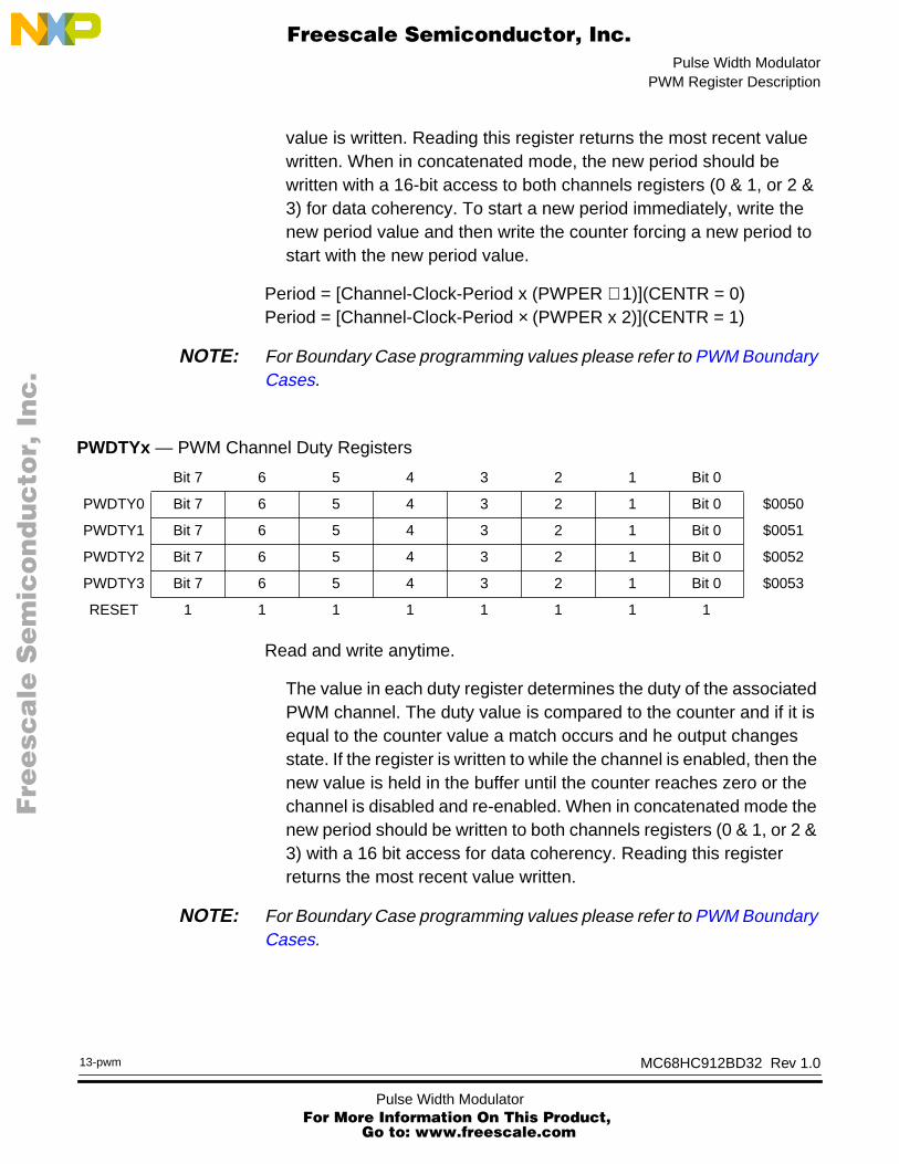
Pulse Width ModulatorPWM Register Description
MC68HC912BD32 Rev 1.0
F
ree
sca
le S
em
ico
nd
uc
tor,
I
Freescale Semiconductor, Inc.n
c..
.
13-pwm
value is written. Reading this register returns the most recent value written. When in concatenated mode, the new period should be written with a 16-bit access to both channels registers (0 & 1, or 2 & 3) for data coherency. To start a new period immediately, write the new period value and then write the counter forcing a new period to start with the new period value.
Period = [Channel-Clock-Period x (PWPER + 1)](CENTR = 0)Period = [Channel-Clock-Period × (PWPER x 2)](CENTR = 1)
NOTE: For Boundary Case programming values please refer to PWM Boundary Cases.
Read and write anytime.
The value in each duty register determines the duty of the associated PWM channel. The duty value is compared to the counter and if it is equal to the counter value a match occurs and he output changes state. If the register is written to while the channel is enabled, then the new value is held in the buffer until the counter reaches zero or the channel is disabled and re-enabled. When in concatenated mode the new period should be written to both channels registers (0 & 1, or 2 & 3) with a 16 bit access for data coherency. Reading this register returns the most recent value written.
NOTE: For Boundary Case programming values please refer to PWM Boundary Cases.
PWDTYx — PWM Channel Duty Registers
Bit 7 6 5 4 3 2 1 Bit 0
PWDTY0 Bit 7 6 5 4 3 2 1 Bit 0 $0050
PWDTY1 Bit 7 6 5 4 3 2 1 Bit 0 $0051
PWDTY2 Bit 7 6 5 4 3 2 1 Bit 0 $0052
PWDTY3 Bit 7 6 5 4 3 2 1 Bit 0 $0053
RESET 1 1 1 1 1 1 1 1
Pulse Width Modulator For More Information On This Product,
Go to: www.freescale.com

Pulse Width Modulator
F
ree
sca
le S
em
ico
nd
uc
tor,
I
Freescale Semiconductor, Inc.n
c..
.
Left-Aligned-Output Mode (CENTR = 0):Duty cycle = [(PWDTYx + 1) / (PWPERx + 1)] × 100% (PPOLx = 1)Duty cycle = [(PWPERx − PWDTYx) / (PWPERx + 1)] × 100%(PPOLx = 0)
Center-Aligned-Output Mode (CENTR = 1):Duty cycle = [(PWPERx − PWDTYx) / PWPERx] × 100% (PPOLx = 1)Duty cycle = (PWDTYx) / (PWPERx) × 100%(PPOLx = 0)
Read and write anytime.
PSWAI — PWM Halts while in Wait Mode0 = Allows PWM main clock generator to continue while in Wait
mode.1 = Halt PWM main clock generator when the part is in Wait mode.
CENTR — Center-Aligned Output Mode
Program change of CENTR bit should be done when PWM channels are disabled. All PWM counters should be written to as the last operation before enabling the channels. Otherwise, asserting/de-asserting the CENTR bit may cause irregularities in the PWM output.
0 = PWM channels operate in Left-Aligned Output mode1 = PWM channels operate in Center-Aligned Output mode
RDP — Reduced Drive of Port P0 = All port P output pins have normal drive capability.1 = All port P output pins have reduced drive capability.
PUPP — Pull-Up Port P Enable0 = All port P pins have an active pull-up device disabled.1 = All port P pins have an active pull-up device enabled.
PWCTL— PWM Control Register $0054
Bit 7 6 5 4 3 2 1 Bit 0
0 0 0 PSWAI CENTR RDP PUPP PSBCK
RESET: 0 0 0 0 0 0 0 0
MC68HC912BD32 Rev 1.0
Pulse Width Modulator For More Information On This Prod
Go to: www.freescale.com
14-pwm
uct,

Pulse Width ModulatorPWM Register Description
MC68HC912BD32 Rev 1.0
F
ree
sca
le S
em
ico
nd
uc
tor,
I
Freescale Semiconductor, Inc.n
c..
.
15-pwm
PSBCK — PWM Stops while in Background Mode0 = Allows PWM to continue while in background mode. This is
useful for emulation.1 = Disable PWM input clock when the part is in background mode.
Read anytime but write only in Special mode (SMOD = 1). These bits are available only in Special mode and are reset in Normal mode.
The PWM has some special test functions which are only accessible when the device is in Special Mode. Special Mode is indicated to the PWM module when the SMOD line on the LIB is asserted.When the SMOD line is asserted, the Special Mode register control bits are accessed via the LIB. When SMOD is not asserted, writes to the Special Mode control bits have no effect ana all bits in the Special Mode register are forced to 0. This ensures that the PWM Special Mode can not be invoked inadvertently during normal operation.
DISCR — Disable Reset of Channel Counter on Write to Channel Counter
0 = Normal operation. Write to PWM channel counter will reset channel counter.
1 = Write to PWM channel counter does not reset channel counter.
DISCP — Disable Compare Count Period0 = Normal Operation1 = In Left-Aligned Output mode, match of period does not reset the
associated PWM counter register.
DISCAL — Disable load of Scale-counters on write to the associated scale-registers
0 = Normal Operation1 = Write to PWSCAL0 and PWSCAL1 does not load scale
counters
PWTST— PWM Special Mode Register (“Test”) $0055
Bit 7 6 5 4 3 2 1 Bit 0
DISCR DISCP DISCAL 0 0 0 0 0
RESET: 0 0 0 0 0 0 0 0
Pulse Width Modulator For More Information On This Product,
Go to: www.freescale.com

Pulse Width Modulator
F
ree
sca
le S
em
ico
nd
uc
tor,
I
Freescale Semiconductor, Inc.n
c..
.
PWM functions share port P pins 3 to 0 and take precedence over the general-purpose port when enabled.
READ: any time (input configured pin return pin level; output configured pin return internal latch pin driver input level.WRITE: Data stored in an internal latch (drives pins only if configured for output and corresponding PWM channel not enabled).
NOTE: Writes do not change pin state when pin is configured for PWM outputs, only after the PWM channel becomes available on port P pin, see PWEN bit description.
.
This register determines whether each pin is input or output when it is selected to be a general purpose I/O pin. Reading Port P Data Register always follows pin data associated with he Port P Data Direction bit. Read and write any time.
DDRP[7:0] — Data Direction Port P pins0 = Configure I/O pin for input only1 = Configure I/O for output
PORTPP — Port P Data Register $0056
Bit 7 6 5 4 3 2 1 Bit 0
PP7 PP6 PP5 PP4 PP3 PP2 PP1 PP0
PWM – – – – PWM3 PWM2 PWM1 PWM0
RESET: – – – – – – – –
PORTPD — Port P Data Direction Register $0057
Bit 7 6 5 4 3 2 1 Bit 0
DDP7 DDP6 DDP5 DDP4 DDP3 DDP2 DDP1 DDP0
RESET: 0 0 0 0 0 0 0 0
MC68HC912BD32 Rev 1.0
Pulse Width Modulator For More Information On This Prod
Go to: www.freescale.com
16-pwm
uct,

Pulse Width ModulatorPWM Boundary Cases
MC68HC912BD32 Rev 1.0
F
ree
sca
le S
em
ico
nd
uc
tor,
I
Freescale Semiconductor, Inc.n
c..
.
17-pwm
PWM Boundary Cases
The boundary conditions for the PWM channel duty registers and the PWM channel period registers cause these results:
Table 24 PWM Boundary Conditions
PWDTYx PWPERx PPOLx Output
$FF >$00 1 Low
$FF >$00 0 High
≥PWPERx – 1 High
≥PWPERx – 0 Low
– $00 1 High
– $00 0 Low
Pulse Width Modulator For More Information On This Product,
Go to: www.freescale.com

Pulse Width Modulator
F
ree
sca
le S
em
ico
nd
uc
tor,
I
Freescale Semiconductor, Inc.n
c..
.
MC68HC912BD32 Rev 1.0
Pulse Width Modulator For More Information On This Prod
Go to: www.freescale.com
18-pwm
uct,

F
ree
sca
le S
em
ico
nd
uc
tor,
IFreescale Semiconductor, Inc.
nc
...
Standard Timer ModuleStandard Timer Module
Contents
Introduction . . . . . . . . . . . . . . . . . . . . . . . . . . . . . . . . . . . . . . . . . . . . 127Timer Registers. . . . . . . . . . . . . . . . . . . . . . . . . . . . . . . . . . . . . . . . . 129Timer Operation in Modes. . . . . . . . . . . . . . . . . . . . . . . . . . . . . . . . . 142
Introduction
The standard timer module consists of a 16-bit software-programmable counter driven by a prescaler. It contains eight complete 16-bit input capture/output compare channels and one 16-bit pulse accumulator.
This timer can be used for many purposes, including input waveform measurements while simultaneously generating an output waveform. Pulse widths can vary from less than a microsecond to many seconds. It can also generate PWM signals without CPU intervention.
MC68HC912BD32 Rev 1.0
1-timerStandard Timer Module For More Information On This Product,
Go to: www.freescale.com

Standard Timer Module
F
ree
sca
le S
em
ico
nd
uc
tor,
I
Freescale Semiconductor, Inc.n
c..
.
Figure 18 Timer Block Diagram: Input Capture, Output Compare, Pulse Accumulator
TFF
PAD
INT
OC7
PADINT
MUX
PAMOD
PULSE ACCUMULATOR
CONTROL REGISTERS
÷ 64
TC7PIN
LOGIC
MODULECLOCK
16-BITCOUNTER
BUFFERLATCH
TC7INPUT
PIN
POLARITYCTL
GATE CLOCKCTL
TIMPTPIN
LOGIC
FUNCTION,DIRECTION,
ANDPOLARITY
CTL
CONTROL REGISTERSPRESCALERDIVIDE CTL
TCTL1 &TCTL2
INPUT CAPTURE/OUTPUT COMPARE
REGISTER
16-BITCOMPARATOR
INTE
RM
OD
ULE
BU
S
OCOUTPUT
ICINPUT
BUFFERLATCH - TIOC
TCRE(COUNTER RESET)
TCNTRESET
TCNT
16-BITCOUNTERPRESCALER
PR2, PR1, PR0
TIMERCOUNT
REGISTER
MODULECLOCK
MC68HC912BD32 Rev 1.0
Standard Timer Module For More Information On This Prod
Go to: www.freescale.com
2-timer
uct,

Standard Timer ModuleTimer Registers
F
ree
sca
le S
em
ico
nd
uc
tor,
I
Freescale Semiconductor, Inc.n
c..
.
Timer Registers
Input/output pins default to general-purpose I/O lines until an internal function which uses that pin is specifically enabled. The timer overrides the state of the DDR to force the I/O state of each associated port line when an output compare using a port line is enabled. In these cases the data direction bits will have no affect on these lines.
When a pin is assigned to output an on-chip peripheral function, writing to this PORTTn bit does not affect the pin but the data is stored in an internal latch such that if the pin becomes available for general-purpose output the driven level will be the last value written to the PORTTn bit.
Read or write anytime.
IOS[7:0] — Input Capture or Output Compare Channel Configuration0 = The corresponding channel acts as an input capture1 = The corresponding channel acts as an output compare.
Read anytime but will always return $00 (1 state is transient). Write anytime.
FOC[7:0] — Force Output Compare Action for Channel 7-0
A write to this register with the corresponding data bit(s) set causes the action which is programmed for output compare “n” to occur immediately. The action taken is the same as if a successful comparison had just taken place with the TCn register except the interrupt flag does not get set.
TIOS — Timer Input Capture/Output Compare Select $0080
Bit 7 6 5 4 3 2 1 Bit 0
IOS7 IOS6 IOS5 IOS4 IOS3 IOS2 IOS1 IOS0
RESET: 0 0 0 0 0 0 0 0
CFORC — Timer Compare Force Register $0081
Bit 7 6 5 4 3 2 1 Bit 0
FOC7 FOC6 FOC5 FOC4 FOC3 FOC2 FOC1 FOC0
RESET: 0 0 0 0 0 0 0 0
MC68HC912BD32 Rev 1.0
3-timerStandard Timer Module For More Information On This Product,
Go to: www.freescale.com
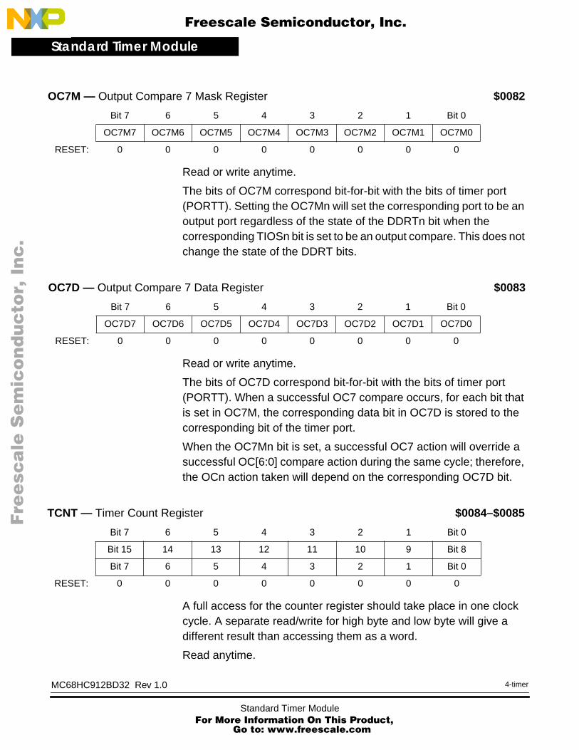
Standard Timer Module
F
ree
sca
le S
em
ico
nd
uc
tor,
I
Freescale Semiconductor, Inc.n
c..
.
Read or write anytime.
The bits of OC7M correspond bit-for-bit with the bits of timer port (PORTT). Setting the OC7Mn will set the corresponding port to be an output port regardless of the state of the DDRTn bit when the corresponding TIOSn bit is set to be an output compare. This does not change the state of the DDRT bits.
Read or write anytime.
The bits of OC7D correspond bit-for-bit with the bits of timer port (PORTT). When a successful OC7 compare occurs, for each bit that is set in OC7M, the corresponding data bit in OC7D is stored to the corresponding bit of the timer port.
When the OC7Mn bit is set, a successful OC7 action will override a successful OC[6:0] compare action during the same cycle; therefore, the OCn action taken will depend on the corresponding OC7D bit.
A full access for the counter register should take place in one clock cycle. A separate read/write for high byte and low byte will give a different result than accessing them as a word.
Read anytime.
OC7M — Output Compare 7 Mask Register $0082
Bit 7 6 5 4 3 2 1 Bit 0
OC7M7 OC7M6 OC7M5 OC7M4 OC7M3 OC7M2 OC7M1 OC7M0
RESET: 0 0 0 0 0 0 0 0
OC7D — Output Compare 7 Data Register $0083
Bit 7 6 5 4 3 2 1 Bit 0
OC7D7 OC7D6 OC7D5 OC7D4 OC7D3 OC7D2 OC7D1 OC7D0
RESET: 0 0 0 0 0 0 0 0
TCNT — Timer Count Register $0084–$0085
Bit 7 6 5 4 3 2 1 Bit 0
Bit 15 14 13 12 11 10 9 Bit 8
Bit 7 6 5 4 3 2 1 Bit 0
RESET: 0 0 0 0 0 0 0 0
MC68HC912BD32 Rev 1.0
Standard Timer Module For More Information On This Prod
Go to: www.freescale.com
4-timer
uct,

Standard Timer ModuleTimer Registers
F
ree
sca
le S
em
ico
nd
uc
tor,
I
Freescale Semiconductor, Inc.n
c..
.
Write has no meaning or effect in the normal mode; only writable in special modes (SMODN = 0).
The period of the first count after a write to the TCNT registers may be a different size because the write is not synchronized with the prescaler clock.
Read or write anytime.
TEN — Timer Enable0 = Disables the timer, including the counter. Can be used for
reducing power consumption.1 = Allows the timer to function normally.
If for any reason the timer is not active, there is no ÷64 clock for the pulse accumulator since the E÷64 is generated by the timer prescaler.
TSWAI — Timer Stops While in Wait0 = Allows the timer to continue running during wait.1 = Disables the timer when the MCU is in the wait mode. Timer
interrupts cannot be used to get the MCU out of wait.
TSBCK — Timer Stops While in Background Mode0 = Allows the timer to continue running while in background mode.1 = Disables the timer whenever the MCU is in background mode.
This is useful for emulation.
TFFCA — Timer Fast Flag Clear All0 = Allows the timer flag clearing to function normally.1 = For TFLG1($8E), a read from an input capture or a write to the
output compare channel ($90–$9F) causes the corresponding channel flag, CnF, to be cleared. For TFLG2 ($8F), any access to the TCNT register ($84, $85) clears the TOF flag. Any access to the PACNT register ($A2, $A3) clears the PAOVF and PAIF flags in the PAFLG register ($A1). This has the
TSCR — Timer System Control Register $0086
Bit 7 6 5 4 3 2 1 Bit 0
TEN TSWAI TSBCK TFFCA 0 0 0 0
RESET: 0 0 0 0 0 0 0 0
MC68HC912BD32 Rev 1.0
5-timerStandard Timer Module For More Information On This Product,
Go to: www.freescale.com

Standard Timer Module
F
ree
sca
le S
em
ico
nd
uc
tor,
I
Freescale Semiconductor, Inc.n
c..
.
advantage of eliminating software overhead in a separate clear sequence. Extra care is required to avoid accidental flag clearing due to unintended accesses.
Read or write anytime.
OMn — Output Mode
OLn — Output Level
These eight pairs of control bits are encoded to specify the output action to be taken as a result of a successful OCn compare. When either OMn or OLn is one, the pin associated with OCn becomes an output tied to OCn regardless of the state of the associated DDRT bit.
TQCR — Reserved $0087
Bit 7 6 5 4 3 2 1 Bit 0
0 0 0 0 0 0 0 0
RESET: 0 0 0 0 0 0 0 0
TCTL1 — Timer Control Register 1 $0088
Bit 7 6 5 4 3 2 1 Bit 0
OM7 OL7 OM6 OL6 OM5 OL5 OM4 OL4
RESET: 0 0 0 0 0 0 0 0
TCTL2 — Timer Control Register 2 $0089
Bit 7 6 5 4 3 2 1 Bit 0
OM3 OL3 OM2 OL2 OM1 OL1 OM0 OL0
RESET: 0 0 0 0 0 0 0 0
Table 25 Compare Result Output Action
OMn OLn Action
0 0 Timer disconnected from output pin logic
0 1 Toggle OCn output line
1 0 Clear OCn output line to zero
1 1 Set OCn output line to one
MC68HC912BD32 Rev 1.0
Standard Timer Module For More Information On This Prod
Go to: www.freescale.com
6-timer
uct,

Standard Timer ModuleTimer Registers
MC68HC912BD32 Rev 1.0
F
ree
sca
le S
em
ico
nd
uc
tor,
I
Freescale Semiconductor, Inc.n
c..
.
7-timer
Read or write anytime.
EDGnB, EDGnA — Input Capture edge control
These eight pairs of control bits configure the input capture edge detector circuits.
The bits in TMSK1 correspond bit-for-bit with the bits in the TFLG1 status register. If cleared, the corresponding flag is disabled from causing a hardware interrupt. If set, the corresponding flag is enabled to cause a hardware interrupt.
Read or write anytime.
C7I–C0I—Input Capture/Output Compare “x” Interrupt enable.
TCTL3 — Timer Control Register 3 $008A
Bit 7 6 5 4 3 2 1 Bit 0
EDG7B EDG7A EDG6B EDG6A EDG5B EDG5A EDG4B EDG4A
RESET: 0 0 0 0 0 0 0 0
TCTL4 — Timer Control Register 4 $008B
Bit 7 6 5 4 3 2 1 Bit 0
EDG3B EDG3A EDG2B EDG2A EDG1B EDG1A EDG0B EDG0A
RESET: 0 0 0 0 0 0 0 0
Table 26 Edge Detector Circuit Configuration
EDGnB EDGnA Configuration
0 0 Capture disabled
0 1 Capture on rising edges only
1 0 Capture on falling edges only
1 1 Capture on any edge (rising or falling)
TMSK1 — Timer Interrupt Mask 1 $008C
Bit 7 6 5 4 3 2 1 Bit 0
C7I C6I C5I C4I C3I C2I C1I C0I
RESET: 0 0 0 0 0 0 0 0
Standard Timer Module For More Information On This Product,
Go to: www.freescale.com

Standard Timer Module
F
ree
sca
le S
em
ico
nd
uc
tor,
I
Freescale Semiconductor, Inc.n
c..
.
Read or write anytime.
TOI — Timer Overflow Interrupt Enable0 = Interrupt inhibited1 = Hardware interrupt requested when TOF flag set
PUPT — Timer Pull-Up Resistor Enable
This enable bit controls pull-up resistors on the timer port pins when the pins are configured as inputs.
1 = Enable pull-up resistor function0 = Disable pull-up resistor function
RDPT — Timer Drive Reduction
This bit reduces the effective output driver size which can reduce power supply current and generated noise depending upon pin loading.
1 = Enable output drive reduction function0 = Normal output drive capability
TCRE — Timer Counter Reset Enable
This bit allows the timer counter to be reset by a successful output compare 7 event.
0 = Counter reset inhibited and counter free runs1 = Counter reset by a successful output compare 7
If TC7 = $0000 and TCRE = 1, TCNT will stay at $0000 continuously. If TC7 = $FFFF and TCRE = 1, TOF will never get set even though TCNT will count from $0000 through $FFFF.
PR2, PR1, PR0 — Timer Prescaler Select
These three bits specify the number of ÷2 stages that are to be inserted between the module clock and the timer counter.
TMSK2 — Timer Interrupt Mask 2 $008D
Bit 7 6 5 4 3 2 1 Bit 0
TOI 0 PUPT RDPT TCRE PR2 PR1 PR0
RESET: 0 0 0 0 0 0 0 0
MC68HC912BD32 Rev 1.0
Standard Timer Module For More Information On This Prod
Go to: www.freescale.com
8-timer
uct,

Standard Timer ModuleTimer Registers
MC68HC912BD32 Rev 1.0
F
ree
sca
le S
em
ico
nd
uc
tor,
I
Freescale Semiconductor, Inc.n
c..
.
9-timer
The newly selected prescale factor will not take effect until the next synchronized edge where all prescale counter stages equal zero.
TFLG1 indicates when interrupt conditions have occurred. To clear a bit in the flag register, write a one to the bit.
Read anytime. Write used in the clearing mechanism (set bits cause corresponding bits to be cleared). Writing a zero will not effect current status of the bit.
When TFFCA bit in TSCR register is set, a read from an input capture or a write into an output compare channel ($90–$9F) will cause the corresponding channel flag CnF to be cleared.
C7F–C0F — Input Capture/Output Compare Channel “n” Flag.
Table 27 Prescaler Selection
PR2 PR1 PR0 Prescale Factor
0 0 0 1
0 0 1 2
0 1 0 4
0 1 1 8
1 0 0 16
1 0 1 32
1 1 0 Reserved
1 1 1 Reserved
TFLG1 — Timer Interrupt Flag 1 $008E
Bit 7 6 5 4 3 2 1 Bit 0
C7F C6F C5F C4F C3F C2F C1F C0F
RESET: 0 0 0 0 0 0 0 0
Standard Timer Module For More Information On This Product,
Go to: www.freescale.com
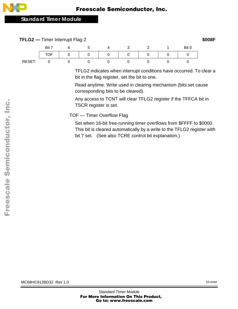
Standard Timer Module
F
ree
sca
le S
em
ico
nd
uc
tor,
I
Freescale Semiconductor, Inc.n
c..
.
TFLG2 indicates when interrupt conditions have occurred. To clear a bit in the flag register, set the bit to one.
Read anytime. Write used in clearing mechanism (bits set cause corresponding bits to be cleared).
Any access to TCNT will clear TFLG2 register if the TFFCA bit in TSCR register is set.
TOF — Timer Overflow Flag
Set when 16-bit free-running timer overflows from $FFFF to $0000. This bit is cleared automatically by a write to the TFLG2 register with bit 7 set. (See also TCRE control bit explanation.)
TFLG2 — Timer Interrupt Flag 2 $008F
Bit 7 6 5 4 3 2 1 Bit 0
TOF 0 0 0 0 0 0 0
RESET: 0 0 0 0 0 0 0 0
MC68HC912BD32 Rev 1.0
Standard Timer Module For More Information On This Prod
Go to: www.freescale.com
10-timer
uct,

Standard Timer ModuleTimer Registers
MC68HC912BD32 Rev 1.0
F
ree
sca
le S
em
ico
nd
uc
tor,
I
Freescale Semiconductor, Inc.n
c..
.
11-timer
TC0 — Timer Input Capture/Output Compare Register 0 $0090–$0091Bit 7 6 5 4 3 2 1 Bit 0
Bit 15 14 13 12 11 10 9 Bit 8
Bit 7 6 5 4 3 2 1 Bit 0
TC1 — Timer Input Capture/Output Compare Register 1 $0092–$0093Bit 7 6 5 4 3 2 1 Bit 0
Bit 15 14 13 12 11 10 9 Bit 8
Bit 7 6 5 4 3 2 1 Bit 0
TC2 — Timer Input Capture/Output Compare Register 2 $0094–$0095Bit 7 6 5 4 3 2 1 Bit 0
Bit 15 14 13 12 11 10 9 Bit 8
Bit 7 6 5 4 3 2 1 Bit 0
TC3 — Timer Input Capture/Output Compare Register 3 $0096–$0097Bit 7 6 5 4 3 2 1 Bit 0
Bit 15 14 13 12 11 10 9 Bit 8
Bit 7 6 5 4 3 2 1 Bit 0
TC4 — Timer Input Capture/Output Compare Register 4 $0098–$0099Bit 7 6 5 4 3 2 1 Bit 0
Bit 15 14 13 12 11 10 9 Bit 8
Bit 7 6 5 4 3 2 1 Bit 0
TC5 — Timer Input Capture/Output Compare Register 5 $009A–$009BBit 7 6 5 4 3 2 1 Bit 0
Bit 15 14 13 12 11 10 9 Bit 8
Bit 7 6 5 4 3 2 1 Bit 0
TC6 — Timer Input Capture/Output Compare Register 6 $009C–$009DBit 7 6 5 4 3 2 1 Bit 0
Bit 15 14 13 12 11 10 9 Bit 8
Bit 7 6 5 4 3 2 1 Bit 0
TC7 — Timer Input Capture/Output Compare Register 7 $009E–$009FBit 7 6 5 4 3 2 1 Bit 0
Bit 15 14 13 12 11 10 9 Bit 8
Bit 7 6 5 4 3 2 1 Bit 0
Standard Timer Module For More Information On This Product,
Go to: www.freescale.com
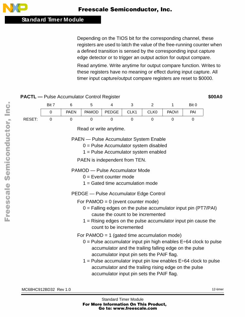
Standard Timer Module
F
ree
sca
le S
em
ico
nd
uc
tor,
I
Freescale Semiconductor, Inc.n
c..
.
Depending on the TIOS bit for the corresponding channel, these registers are used to latch the value of the free-running counter when a defined transition is sensed by the corresponding input capture edge detector or to trigger an output action for output compare.
Read anytime. Write anytime for output compare function. Writes to these registers have no meaning or effect during input capture. All timer input capture/output compare registers are reset to $0000.
Read or write anytime.
PAEN — Pulse Accumulator System Enable0 = Pulse Accumulator system disabled1 = Pulse Accumulator system enabled
PAEN is independent from TEN.
PAMOD — Pulse Accumulator Mode0 = Event counter mode1 = Gated time accumulation mode
PEDGE — Pulse Accumulator Edge Control
For PAMOD = 0 (event counter mode)0 = Falling edges on the pulse accumulator input pin (PT7/PAI)
cause the count to be incremented1 = Rising edges on the pulse accumulator input pin cause the
count to be incremented
For PAMOD = 1 (gated time accumulation mode)0 = Pulse accumulator input pin high enables E÷64 clock to pulse
accumulator and the trailing falling edge on the pulse accumulator input pin sets the PAIF flag.
1 = Pulse accumulator input pin low enables E÷64 clock to pulse accumulator and the trailing rising edge on the pulse accumulator input pin sets the PAIF flag.
PACTL — Pulse Accumulator Control Register $00A0
Bit 7 6 5 4 3 2 1 Bit 0
0 PAEN PAMOD PEDGE CLK1 CLK0 PAOVI PAI
RESET: 0 0 0 0 0 0 0 0
MC68HC912BD32 Rev 1.0
Standard Timer Module For More Information On This Prod
Go to: www.freescale.com
12-timer
uct,

Standard Timer ModuleTimer Registers
MC68HC912BD32 Rev 1.0
F
ree
sca
le S
em
ico
nd
uc
tor,
I
Freescale Semiconductor, Inc.n
c..
.
13-timer
If the timer is not active (TEN = 0 in TSCR), there is no ÷64 clock since the E÷64 clock is generated by the timer prescaler.
CLK1, CLK0 — Clock Select Register
If the pulse accumulator is disabled (PAEN = 0), the prescaler clock from the timer is always used as an input clock to the timer counter. The change from one selected clock to the other happens immediately after these bits are written.
PAOVI — Pulse Accumulator Overflow Interrupt Enable0 = Interrupt inhibited1 = Interrupt requested if PAOVF is set
PAI — Pulse Accumulator Input Interrupt Enable0 = Interrupt inhibited1 = Interrupt requested if PAIF is set
Read or write anytime.
When TFFCA bit in the TSCR register is set, any access to the PACNT register will clear all the flags in the PAFLG register.
PAOVF — Pulse Accumulator Overflow Flag
Set when the 16-bit pulse accumulator overflows from $FFFF to $0000. This bit is cleared automatically by a write to the PAFLG register with bit 1 set.
Table 28 Clock Selection
CLK1 CLK0 Selected Clock
0 0 Use timer prescaler clock as timer counter clock
0 1 Use PACLK as input to timer counter clock
1 0 Use PACLK/256 as timer counter clock frequency
1 1 Use PACLK/65536 as timer counter clock frequency
PAFLG — Pulse Accumulator Flag Register $00A1
Bit 7 6 5 4 3 2 1 Bit 0
0 0 0 0 0 0 PAOVF PAIF
RESET: 0 0 0 0 0 0 0 0
Standard Timer Module For More Information On This Product,
Go to: www.freescale.com

Standard Timer Module
F
ree
sca
le S
em
ico
nd
uc
tor,
I
Freescale Semiconductor, Inc.n
c..
.
PAIF — Pulse Accumulator Input Edge Flag
Set when the selected edge is detected at the pulse accumulator input pin. In event mode, the event edge triggers PAIF. In gated time accumulation mode, the trailing edge of the gate signal at the pulse accumulator input pin triggers PAIF. This bit is cleared automatically by a write to the PAFLG register with bit 0 set.
Full count register access should take place in one clock cycle. A separate read/write for high byte and low byte will give a different result than accessing them as a word.
Read or write anytime.
Read anytime. Write only in special mode (SMODN = 0)
TCBYP — Timer Divider Chain Bypass0 = Normal operation1 = The 16-bit free-running timer counter is divided into two 8-bit
halves and the prescaler is bypassed. The clock drives both halves directly.
PCBYP — Pulse Accumulator Divider Chain Bypass0 = Normal operation1 = The 16-bit pulse accumulator counter is divided into two 8-bit
halves and the prescaler is bypassed. The clock drives both halves directly.
PACNT — 16-bit Pulse Accumulator Count Register $00A2–$00A3
Bit 7 6 5 4 3 2 1 Bit 0
Bit 15 14 13 12 11 10 9 Bit 8
Bit 7 6 5 4 3 2 1 Bit 0
RESET: 0 0 0 0 0 0 0 0
TIMTST — Timer Test Register $00AD
Bit 7 6 5 4 3 2 1 Bit 0
0 0 0 0 0 0 TCBYP PCBYP
RESET: 0 0 0 0 0 0 0 0
MC68HC912BD32 Rev 1.0
Standard Timer Module For More Information On This Prod
Go to: www.freescale.com
14-timer
uct,

Standard Timer ModuleTimer Registers
MC68HC912BD32 Rev 1.0
F
ree
sca
le S
em
ico
nd
uc
tor,
I
Freescale Semiconductor, Inc.n
c..
.
15-timer
PORTT can be read anytime. When configured as an input, a read will return the pin level. When configured as output, a read will return the latched output data.
NOTE: Writes do not change pin state when the pin is configured for timer output. The minimum pulse width for pulse accumulator input should always be greater than two module clocks due to input synchronizer circuitry. The minimum pulse width for the input capture should always be greater than the width of two module clocks due to input synchronizer circuitry.
Read or write anytime.0 = Configures the corresponding I/O pin for input only1 = Configures the corresponding I/O pin for output
The timer forces the I/O state to be an output for each timer port pin associated with an enabled output compare. In these cases the data direction bits will not be changed but have no affect on the direction of these pins. The DDRT will revert to controlling the I/O direction of a pin when the associated timer output compare is disabled. Input captures do not override the DDRT settings.
PORTT — Timer Port Data Register $00AE
Bit 7 6 5 4 3 2 1 Bit 0
PT7 PT6 PT5 PT4 PT3 PT2 PT1 PT0
TIMER I/OC7 I/OC6 I/OC5 I/OC4 I/OC3 I/OC2 I/OC1 I/OC0
PA PAI
DDRT — Data Direction Register for Timer Port $00AF
Bit 7 6 5 4 3 2 1 Bit 0
DDT7 DDT6 DDT5 DDT4 DDT3 DDT2 DDT1 DDT0
RESET: 0 0 0 0 0 0 0 0
Standard Timer Module For More Information On This Product,
Go to: www.freescale.com

Standard Timer Module
F
ree
sca
le S
em
ico
nd
uc
tor,
I
Freescale Semiconductor, Inc.n
c..
.
Timer Operation in Modes
STOP: Timer is off since both PCLK and ECLK are stopped.
BDM: Timer keeps running, unless TSBCK = 1
WAIT: Counters keep running, unless TSWAI = 1
NORMAL: Timer keeps running, unless TEN = 0
TEN = 0: All timer operations are stopped, registers may be accessed.Gated pulse accumulator ÷64 clock is also disabled.
PAEN = 0: All pulse accumulator operations are stopped, registers may be accessed.
MC68HC912BD32 Rev 1.0
Standard Timer Module For More Information On This Prod
Go to: www.freescale.com
16-timer
uct,

F
ree
sca
le S
em
ico
nd
uc
tor,
IFreescale Semiconductor, Inc.
nc
...
Serial InterfaceSerial Interface
Contents
Introduction . . . . . . . . . . . . . . . . . . . . . . . . . . . . . . . . . . . . . . . . . . . . 143Block diagram . . . . . . . . . . . . . . . . . . . . . . . . . . . . . . . . . . . . . . . . . . 144Serial Communication Interface (SCI). . . . . . . . . . . . . . . . . . . . . . . . 144Serial Peripheral Interface (SPI) . . . . . . . . . . . . . . . . . . . . . . . . . . . . 155Port S . . . . . . . . . . . . . . . . . . . . . . . . . . . . . . . . . . . . . . . . . . . . . . . . 164
Introduction
The serial interface of the MC68HC912BD32 consists of two independent serial I/O sub-systems: the serial communication interface (SCI) and the serial peripheral interface (SPI). Each serial pin shares function with the general-purpose port pins of port S. The SCI is an NRZ type system that is compatible with standard RS-232 systems. The SCI system has a single wire operation mode which allows the unused pin to be available as general-purpose I/O. The SPI subsystem, which is compatible with the M68HC11 SPI, includes new features such as SS output and bidirectional mode.
MC68HC912BD32 Rev 1.0
1-sintSerial Interface For More Information On This Product,
Go to: www.freescale.com

Serial Interface
F
ree
sca
le S
em
ico
nd
uc
tor,
I
Freescale Semiconductor, Inc.n
c..
.
Block diagram
Figure 19 Serial Interface Block Diagram
Serial Communication Interface (SCI)
The serial communication interface on the MC68HC912BD32 is an NRZ format (one start, eight or nine data, and one stop bit) asynchronous communication system with independent internal baud rate generation circuitry and an SCI transmitter and receiver. It can be configured for eight or nine data bits (one of which may be designated as a parity bit, odd or even). If enabled, parity is generated in hardware for transmitted and received data. Receiver parity errors are flagged in hardware. The baud rate generator is based on a modulus counter, allowing flexibility in choosing baud rates. There is a receiver wake-up feature, an idle line detect feature, a loop-back mode, and various error detection features. Two port pins provide the external interface for the transmitted data (TXD) and the received data (RXD).
SCI
I/O
SPI
DD
RS/
IOC
TLR
PO
RT
S I/O
DR
IVER
S
SERIALINTERFACE
PS0
PS1
PS2
PS3
PS4
PS5
PS6
PS7
RxD
TxD
MISO/SISO
MOSI/MOMI
SCK
CS/SS
I/O
I/O
MC68HC912BD32 Rev 1.0
Serial Interface For More Information On This Prod
Go to: www.freescale.com
2-sint
uct,

Serial InterfaceSerial Communication Interface (SCI)
F
ree
sca
le S
em
ico
nd
uc
tor,
I
Freescale Semiconductor, Inc.n
c..
.
Figure 20 Serial Communications Interface Block Diagram
Data Format The serial data format requires the following conditions:
• An idle-line in the high state before transmission or reception of a message.
• A start bit (logic zero), transmitted or received, that indicates the start of each character.
Rx Baud Rate
Tx Baud Rate
MCLK
DIVIDER 10-11 BIT SHIFT REG
MSB
TxD BUFFER/SC0DRL
TxMTR CONTROL
SC0CR2/SCI CTL 2
SC0CR1/SCI CTL 1
SC0SR1/INT STATUS
DATA RECOVERY
10-11 BIT SHIFT REG
TxD BUFFER/SC0DRL
SC0BD/SELECT
LSB
RxD
TxD
PIN
CO
NTR
OL
/ DD
RS
/ PO
RT
S
WAKE-UP LOGICSC0CR1/SCI CTL 1
SC0SR1/INT STATUS
SC0CR2/SCI CTL 2
INT REQUEST LOGIC
MSB LSB
INT REQUEST LOGIC
SCI RECEIVER
SCI TRANSMITTER
DATA BUS
PARITYDETECT
PARITYGENERATOR
TO INTERNAL
LOGIC
BAUD RATECLOCK
PS0
PS1
MC68HC912BD32 Rev 1.0
3-sintSerial Interface For More Information On This Product,
Go to: www.freescale.com

Serial Interface
F
ree
sca
le S
em
ico
nd
uc
tor,
I
Freescale Semiconductor, Inc.n
c..
.
• Data that is transmitted or received least significant bit (LSB) first.
• A stop bit (logic one), used to indicate the end of a frame. (A frame consists of a start bit, a character of eight or nine data bits and a stop bit.)
• A BREAK is defined as the transmission or reception of a logic zero for one frame or more.
• This SCI supports hardware parity for transmit and receive.
SCI Baud Rate Generation
The basis of the SCI baud rate generator is a 13-bit modulus counter. This counter gives the generator the flexibility necessary to achieve a reasonable level of independence from the CPU operating frequency and still be able to produce standard baud rates with a minimal amount of error. The clock source for the generator comes from the P Clock.
Register Descriptions
Control and data registers for the SCI subsystem are described below. The memory address indicated for each register is the default address that is in use after reset. The entire 512-byte register block can be mapped to any 2K byte boundary within the standard 64K byte address space.
Table 29 Baud Rate Generation
DesiredSCI Baud Rate
BR Divisor forP = 4.0 MHz
BR Divisor forP = 8.0 MHz
BR Divisor forP = 10.0 MHz
110 2273 4545 5682
300 833 1667 2083
600 417 833 1042
1200 208 417 521
2400 104 208 260
4800 52 104 130
9600 26 52 65
14400 17 35 43
19200 13 26 33
38400 — 13 16
MC68HC912BD32 Rev 1.0
Serial Interface For More Information On This Prod
Go to: www.freescale.com
4-sint
uct,

Serial InterfaceSerial Communication Interface (SCI)
F
ree
sca
le S
em
ico
nd
uc
tor,
I
Freescale Semiconductor, Inc.n
c..
.
SC0BDH and SC0BDL are considered together as a 16-bit baud rate control register.
Read any time. Write SBR[12:0] anytime. Low order byte must be written for change to take effect. Write SBR[15:13] only in special modes. The value in SBR[12:0] determines the baud rate of the SCI. The desired baud rate is determined by the following formula:
which is equivalent to:
BR is the value written to bits SBR[12:0] to establish baud rate.
NOTE: The baud rate generator is disabled until the TE or RE bit in SC0CR2 register is set for the first time after reset, and/or the baud rate generator is disabled when SBR[12:0] = 0.
BTST — Baud Register Test
Reserved for test function
BSPL — Baud Rate Counter Split
Reserved for test function
BRLD — Baud Rate Reload
Reserved for test function
SC0BDH — SCI Baud Rate Control Register $00C0
Bit 7 6 5 4 3 2 1 Bit 0
BTST BSPL BRLD SBR12 SBR11 SBR10 SBR9 SBR8 High
RESET: 0 0 0 0 0 0 0 0
SC0BDL — SCI Baud Rate Control Register $00C1
Bit 7 6 5 4 3 2 1 Bit 0
SBR7 SBR6 SBR5 SBR4 SBR3 SBR2 SBR1 SBR0 Low
RESET: 0 0 0 0 0 1 0 0
SCI Baud Rate MCLK16 BR×--------------------=
BR MCLK16 SCI Baud Rate×------------------------------------------------=
MC68HC912BD32 Rev 1.0
5-sintSerial Interface For More Information On This Product,
Go to: www.freescale.com

Serial Interface
F
ree
sca
le S
em
ico
nd
uc
tor,
I
Freescale Semiconductor, Inc.n
c..
.
Read or write anytime.
LOOPS — SCI LOOP Mode/Single Wire Mode Enable0 = SCI transmit and receive sections operate normally.1 = SCI receive section is disconnected from the RXD pin and the
RXD pin is available as general purpose I/O. The receiver input is determined by the RSRC bit. The transmitter output is controlled by the associated DDRS bit. Both the transmitter and the receiver must be enabled to use the LOOP or the single wire mode.
If the DDRS bit associated with the TXD pin is set during the LOOPS = 1, the TXD pin outputs the SCI waveform. If the DDRS bit associated with the TXD pin is clear during the LOOPS = 1, the TXD pin becomes high (IDLE line state) for RSRC = 0 and high impedance for RSRC = 1. Refer to Table 30.
WOMS — Wired-Or Mode for Serial Pins
This bit controls the two pins (TXD and RXD) associated with the SCI section.
0 = Pins operate in a normal mode with both high and low drive capability. To affect the RXD bit, that bit would have to be configured as an output (via DDRS) which is the single wire case when using the SCI. WOMS bit still affects general purpose output on TXD and RXD pins when SCI is not using these pins.
1 = Each pin operates in an open drain fashion if that pin is declared as an output.
RSRC — Receiver Source
When LOOPS = 1, the RSRC bit determines the internal feedback path for the receiver.
0 = Receiver input is connected to the transmitter internally (not TXD pin)
1 = Receiver input is connected to the TXD pin
SC0CR1 — SCI Control Register 1 $00C2
Bit 7 6 5 4 3 2 1 Bit 0
LOOPS WOMS RSRC M WAKE ILT PE PT
RESET: 0 0 0 0 0 0 0 0
MC68HC912BD32 Rev 1.0
Serial Interface For More Information On This Prod
Go to: www.freescale.com
6-sint
uct,

Serial InterfaceSerial Communication Interface (SCI)
MC68HC912BD32 Rev 1.0
F
ree
sca
le S
em
ico
nd
uc
tor,
I
Freescale Semiconductor, Inc.n
c..
.
7-sint
M — Mode (select character format)0 = One start, eight data, one stop bit1 = One start, eight data, ninth data, one stop bit
WAKE — Wakeup by Address Mark/Idle0 = Wake up by IDLE line recognition1 = Wake up by address mark (last data bit set)
ILT — Idle Line Type
Determines which of two types of idle line detection will be used by the SCI receiver.
0 = Short idle line mode is enabled.1 = Long idle line mode is detected.
In the short mode, the SCI circuitry begins counting ones in the search for the idle line condition immediately after the start bit. This means that the stop bit and any bits that were ones before the stop bit could be counted in that string of ones, resulting in earlier recognition of an idle line.
In the long mode, the SCI circuitry does not begin counting ones in the search for the idle line condition until a stop bit is received. Therefore, the last byte’s stop bit and preceding “1” bits do not affect how quickly an idle line condition can be detected.
PE — Parity Enable0 = Parity is disabled.1 = Parity is enabled.
Table 30 Loop Mode Functions
LOOPS RSRC DDS1(3) WOMS Function of Port S Bit 1/3
0 x x x Normal Operations
1 0 0 0/1 LOOP mode without TXD output (TXD = High Impedance)
1 0 1 0 LOOP mode with TXD output (CMOS)
1 0 1 1 LOOP mode with TXD output (open-drain)
1 1 0 xSingle wire mode without TXD output
(the pin is used as receiver input only, TXD = High Impedance)
1 1 1 0Single wire mode with TXD output
(the output is also fed back to receiver input, CMOS)
1 1 1 1 Single wire mode for the receiving and transmitting (open-drain)
Serial Interface For More Information On This Product,
Go to: www.freescale.com

Serial Interface
F
ree
sca
le S
em
ico
nd
uc
tor,
I
Freescale Semiconductor, Inc.n
c..
.
PT — Parity Type
If parity is enabled, this bit determines even or odd parity for both the receiver and the transmitter.
0 = Even parity is selected. An even number of ones in the data character causes the parity bit to be zero and an odd number of ones causes the parity bit to be one.
1 = Odd parity is selected. An odd number of ones in the data character causes the parity bit to be zero and an even number of ones causes the parity bit to be one.
Read or write anytime.
TIE — Transmit Interrupt Enable0 = TDRE interrupts disabled1 = SCI interrupt will be requested whenever the TDRE status flag
is set.
TCIE — Transmit Complete Interrupt Enable0 = TC interrupts disabled1 = SCI interrupt will be requested whenever the TC status flag is
set.
RIE — Receiver Interrupt Enable0 = RDRF and OR interrupts disabled1 = SCI interrupt will be requested whenever the RDRF status flag
or the OR status flag is set.
ILIE — Idle Line Interrupt Enable0 = IDLE interrupts disabled1 = SCI interrupt will be requested whenever the IDLE status flag
is set.
SC0CR2 — SCI Control Register 2 $00C3
Bit 7 6 5 4 3 2 1 Bit 0
TIE TCIE RIE ILIE TE RE RWU SBK
RESET: 0 0 0 0 0 0 0 0
MC68HC912BD32 Rev 1.0
Serial Interface For More Information On This Prod
Go to: www.freescale.com
8-sint
uct,
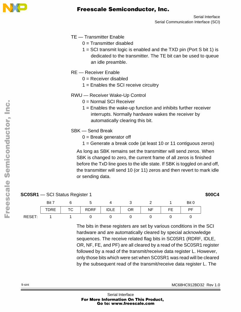
Serial InterfaceSerial Communication Interface (SCI)
MC68HC912BD32 Rev 1.0
F
ree
sca
le S
em
ico
nd
uc
tor,
I
Freescale Semiconductor, Inc.n
c..
.
9-sint
TE — Transmitter Enable0 = Transmitter disabled1 = SCI transmit logic is enabled and the TXD pin (Port S bit 1) is
dedicated to the transmitter. The TE bit can be used to queue an idle preamble.
RE — Receiver Enable0 = Receiver disabled1 = Enables the SCI receive circuitry
RWU — Receiver Wake-Up Control0 = Normal SCI Receiver1 = Enables the wake-up function and inhibits further receiver
interrupts. Normally hardware wakes the receiver by automatically clearing this bit.
SBK — Send Break0 = Break generator off1 = Generate a break code (at least 10 or 11 contiguous zeros)
As long as SBK remains set the transmitter will send zeros. When SBK is changed to zero, the current frame of all zeros is finished before the TxD line goes to the idle state. If SBK is toggled on and off, the transmitter will send 10 (or 11) zeros and then revert to mark idle or sending data.
The bits in these registers are set by various conditions in the SCI hardware and are automatically cleared by special acknowledge sequences. The receive related flag bits in SC0SR1 (RDRF, IDLE, OR, NF, FE, and PF) are all cleared by a read of the SC0SR1 register followed by a read of the transmit/receive data register L. However, only those bits which were set when SC0SR1 was read will be cleared by the subsequent read of the transmit/receive data register L. The
SC0SR1 — SCI Status Register 1 $00C4
Bit 7 6 5 4 3 2 1 Bit 0
TDRE TC RDRF IDLE OR NF FE PF
RESET: 1 1 0 0 0 0 0 0
Serial Interface For More Information On This Product,
Go to: www.freescale.com
Serial Interface
F
ree
sca
le S
em
ico
nd
uc
tor,
I
Freescale Semiconductor, Inc.n
c..
.
transmit related bits in SC0SR1 (TDRE and TC) are cleared by a read of the SC0SR1 register followed by a write to the transmit/receive data register L.
Read anytime (used in auto clearing mechanism). Write has no meaning or effect.
TDRE — Transmit Data Register Empty Flag
New data will not be transmitted unless SC0SR1 is read before writing to the transmit data register. Reset sets this bit.
0 = SC0DR busy1 = Any byte in the transmit data register is transferred to the serial
shift register so new data may now be written to the transmit data register.
TC — Transmit Complete Flag
Flag is set when the transmitter is idle (no data, preamble, or break transmission in progress). Clear by reading SC0SR1 with TC set and then writing to SC0DR.
0 = Transmitter busy1 = Transmitter is idle
RDRF — Receive Data Register Full Flag
Once cleared, IDLE is not set again until the RxD line has been active and becomes idle again. RDRF is set if a received character is ready to be read from SC0DR. Clear the RDRF flag by reading SC0SR1 with RDRF set and then reading SC0DR.
0 = SC0DR empty1 = SC0DR full
IDLE — Idle Line Detected Flag
Receiver idle line is detected (the receipt of a minimum of 10/11 consecutive ones). This bit will not be set by the idle line condition when the RWU bit is set. Once cleared, IDLE will not be set again until after RDRF has been set (after the line has been active and becomes idle again).
0 = RxD line is idle1 = RxD line is active
MC68HC912BD32 Rev 1.0
Serial Interface For More Information On This Prod
Go to: www.freescale.com
10-sint
uct,

Serial InterfaceSerial Communication Interface (SCI)
MC68HC912BD32 Rev 1.0
F
ree
sca
le S
em
ico
nd
uc
tor,
I
Freescale Semiconductor, Inc.n
c..
.
11-sint
OR — Overrun Error Flag
New byte is ready to be transferred from the receive shift register to the receive data register and the receive data register is already full (RDRF bit is set). Data transfer is inhibited until this bit is cleared.
0 = No overrun1 = Overrun detected
NF — Noise Error Flag
Set during the same cycle as the RDRF bit but not set in the case of an overrun (OR).
0 = Unanimous decision1 = Noise on a valid start bit, any of the data bits, or on the stop bit
FE — Framing Error Flag
Set when a zero is detected where a stop bit was expected. Clear the FE flag by reading SC0SR1 with FE set and then reading SC0DR.
0 = Stop bit detected1 = Zero detected rather than a stop bit
PF — Parity Error Flag
Indicates if received data’s parity matches parity bit. This feature is active only when parity is enabled. The type of parity tested for is determined by the PT (parity type) bit in SC0CR1.
0 = Parity correct1 = Incorrect parity detected
Serial Interface For More Information On This Product,
Go to: www.freescale.com

Serial Interface
F
ree
sca
le S
em
ico
nd
uc
tor,
I
Freescale Semiconductor, Inc.n
c..
.
Read anytime. Write has no meaning or effect.
RAF — Receiver Active Flag
This bit is controlled by the receiver front end. It is set during the RT1 time period of the start bit search. It is cleared when an idle state is detected or when the receiver circuitry detects a false start bit (generally due to noise or baud rate mismatch).
0 = A character is not being received1 = A character is being received
R8 — Receive Bit 8
Read anytime. Write has no meaning or affect.
This bit is the ninth serial data bit received when the SCI system is configured for nine-data-bit operation.
T8 — Transmit Bit 8
Read or write anytime.
This bit is the ninth serial data bit transmitted when the SCI system is configured for nine-data-bit operation. When using 9-bit data format this bit does not have to be written for each data word. The same value will be transmitted as the ninth bit until this bit is rewritten.
SC0SR2 — SCI Status Register 2 $00C5
Bit 7 6 5 4 3 2 1 Bit 0
0 0 0 0 0 0 0 RAF
RESET: 0 0 0 0 0 0 0 0
SC0DRH — SCI Data Register High $00C6
Bit 7 6 5 4 3 2 1 Bit 0
R8 T8 0 0 0 0 0 0
RESET: 0 0 0 0 0 0 0 0
SC0DRL — SCI Data Register Low $00C7
Bit 7 6 5 4 3 2 1 Bit 0
R7/T7 R6/T6 R5/T5 R4/T4 R3/T3 R2/T2 R1/T1 R0/T0
RESET: 0 0 0 0 0 0 0 0
MC68HC912BD32 Rev 1.0
Serial Interface For More Information On This Prod
Go to: www.freescale.com
12-sint
uct,

Serial InterfaceSerial Peripheral Interface (SPI)
MC68HC912BD32 Rev 1.0
F
ree
sca
le S
em
ico
nd
uc
tor,
I
Freescale Semiconductor, Inc.n
c..
.
13-sint
R7/T7–R0/T0 — Receive/Transmit Data Bits 7 to 0
Reads access the eight bits of the read-only SCI receive data register (RDR). Writes access the eight bits of the write-only SCI transmit data register (TDR). SC0DRL:SC0DRH form the 9-bit data word for the SCI. If the SCI is being used with a 7- or 8-bit data word, only SC0DRL needs to be accessed. If a 9-bit format is used, the upper register should be written first to ensure that it is transferred to the transmitter shift register with the lower register.
Serial Peripheral Interface (SPI)
The serial peripheral interface allows the MC68HC912BD32 to communicate synchronously with peripheral devices and other microprocessors. The SPI system in the MC68HC912BD32 can operate as a master or as a slave. The SPI is also capable of interprocessor communications in a multiple master system.
When the SPI is enabled, all pins that are defined by the configuration as inputs will be inputs regardless of the state of the DDRS bits for those pins. All pins that are defined as SPI outputs will be outputs only if the DDRS bits for those pins are set. Any SPI output whose corresponding DDRS bit is cleared can be used as a general-purpose input.
A bidirectional serial pin is possible using the DDRS as the direction control.
SPI Baud Rate Generation
The P clock is input to a divider series and the resulting SPI clock rate may be selected to be P divided by 2, 4, 8, 16, 32, 64, 128 or 256. Three bits in the SP0BR register control the SPI clock rate. This baud rate generator is activated only when SPI is in the master mode and serial transfer is taking place. Otherwise this divider is disabled to save power.
SPI Operation In the SPI system the 8-bit data register in the master and the 8-bit data register in the slave are linked to form a distributed 16-bit register. When a data transfer operation is performed, this 16-bit register is serially shifted eight bit positions by the SCK clock from the master so the data
Serial Interface For More Information On This Product,
Go to: www.freescale.com

Serial Interface
F
ree
sca
le S
em
ico
nd
uc
tor,
I
Freescale Semiconductor, Inc.n
c..
.
is effectively exchanged between the master and the slave. Data written to the SP0DR register of the master becomes the output data for the slave and data read from the SP0DR register of the master after a transfer operation is the input data from the slave.
Figure 21 Serial Peripheral Interface Block Diagram
A clock phase control bit (CPHA) and a clock polarity control bit (CPOL) in the SP0CR1 register select one of four possible clock formats to be used by the SPI system. The CPOL bit simply selects non-inverted or inverted clock. The CPHA bit is used to accommodate two fundamentally different protocols by shifting the clock by one half cycle or no phase shift.
PINCONTROL
LOGIC
8-BIT SHIFT REGISTER
READ DATA BUFFER
SHIFT CONTROL LOGIC
CLOCKLOGIC
SPI CONTROL
SP0SR SPI STATUS REGISTER
SP0DR SPI DATA REGISTER
SPIF
WC
OL
MO
DF
DIVIDER
SELECT
SP0BR SPI BAUD RATE REGISTER
÷2 ÷4 ÷8 ÷16 ÷32 ÷64 ÷128 ÷256
SPIINTERRUPT
INTERNAL BUS
MCU P CLOCK(SAME AS E RATE)
SM
M
S
M
S
SP
R2
SP
R1
SP
R0
REQUEST
SPIE
SP
E
MS
TR
CP
OL
CP
HA
LSBF
LSBF
PU
PS
RD
S
SW
OM
SP
C0
SS
OE
SPE
CLOCK
MSTR
SWOM
MISOPS4
SCKPS6
SSPS7
MOSIPS5
SP0CR1 SPI CONTROL REGISTER 1 SP0CR2 SPI CONTROL REGISTER 2
MC68HC912BD32 Rev 1.0
Serial Interface For More Information On This Prod
Go to: www.freescale.com
14-sint
uct,

Serial InterfaceSerial Peripheral Interface (SPI)
MC68HC912BD32 Rev 1.0
F
ree
sca
le S
em
ico
nd
uc
tor,
I
Freescale Semiconductor, Inc.n
c..
.
15-sint
Figure 22 SPI Clock Format 0 (CPHA = 0)
tL
Begin End
SCK (CPOL=0)
SAMPLE I
CHANGE O
SEL SS (O)
Transfer
SCK (CPOL=1)
MSB first (LSBF=0): LSB first (LSBF=1):
MSBLSB
LSBMSB
Bit 5Bit 2
Bit 6Bit 1
Bit 4Bit 3
Bit 3Bit 4
Bit 2Bit 5
Bit 1Bit 6
CHANGE O
SEL SS (I)
(MOSI pin)
(MISO pin)
(Master only)
(MOSI/MISO)
tT
for tT, tl, tLMinimum 1/2 SCK
tI tL
Serial Interface For More Information On This Product,
Go to: www.freescale.com

Serial Interface
F
ree
sca
le S
em
ico
nd
uc
tor,
I
Freescale Semiconductor, Inc.n
c..
.
Figure 23 SPI Clock Format 1 (CPHA = 1)
SS Output Available in master mode only, SS output is enabled with the SSOE bit in the SP0CR1 register if the corresponding DDRS bit is set. The SS output pin will be connected to the SS input pin of the external slave device. The SS output automatically goes low for each transmission to select the external device and it goes high during each idling state to deselect external devices.
tL tT
for tT, tl, tLMinimum 1/2 SCK
tI tL
Begin End
SCK (CPOL=0)
SAMPLE I
CHANGE O
SEL SS (O)
Transfer
SCK (CPOL=1)
MSB first (LSBF=0): LSB first (LSBF=1):
MSBLSB
LSBMSB
Bit 5Bit 2
Bit 6Bit 1
Bit 4Bit 3
Bit 3Bit 4
Bit 2Bit 5
Bit 1Bit 6
CHANGE O
SEL SS (I)
(MOSI pin)
(MISO pin)
(Master only)
(MOSI/MISO)
Table 31 SS Output Selection
DDS7 SSOE Master Mode Slave Mode
0 0 SS Input with MODF Feature SS Input
0 1 Reserved SS Input
1 0 General-Purpose Output SS Input
1 1 SS Output SS Input
MC68HC912BD32 Rev 1.0
Serial Interface For More Information On This Prod
Go to: www.freescale.com
16-sint
uct,

Serial InterfaceSerial Peripheral Interface (SPI)
MC68HC912BD32 Rev 1.0
F
ree
sca
le S
em
ico
nd
uc
tor,
I
Freescale Semiconductor, Inc.n
c..
.
17-sint
Bidirectional Mode (MOMI or SISO)
In bidirectional mode, the SPI uses only one serial data pin for external device interface. The MSTR bit decides which pin to be used. The MOSI pin becomes serial data I/O (MOMI) pin for the master mode, and the MISO pin becomes serial data I/O (SISO) pin for the slave mode. The direction of each serial I/O pin depends on the corresponding DDRS bit.
Figure 24 Normal Mode and Bidirectional Mode
Register Descriptions
Control and data registers for the SPI subsystem are described below. The memory address indicated for each register is the default address that is in use after reset. The entire 512-byte register block can be mapped to any 2K byte boundary within the standard 64K byte address space. For more information refer to Operating Modes.
When SPE=1Master Mode
MSTR=1Slave Mode
MSTR=0
NormalMode
SPC0=0
SWOM enables open drain output. SWOM enables open drain output.
Bidirectional Mode
SPC0=1
SWOM enables open drain output. PS4 becomes GPIO. SWOM enables open drain output. PS5 becomes GPIO.
SPI
MO
MI
DDS5
Serial Out
Serial In
SPI
SI
SO
Serial In
Serial Out
DDS4
SPI
MOMI
PS4
DDS5
Serial Out
Serial In
SPI
PS5
SISO
DDS4
Serial In
Serial Out
Serial Interface For More Information On This Product,
Go to: www.freescale.com
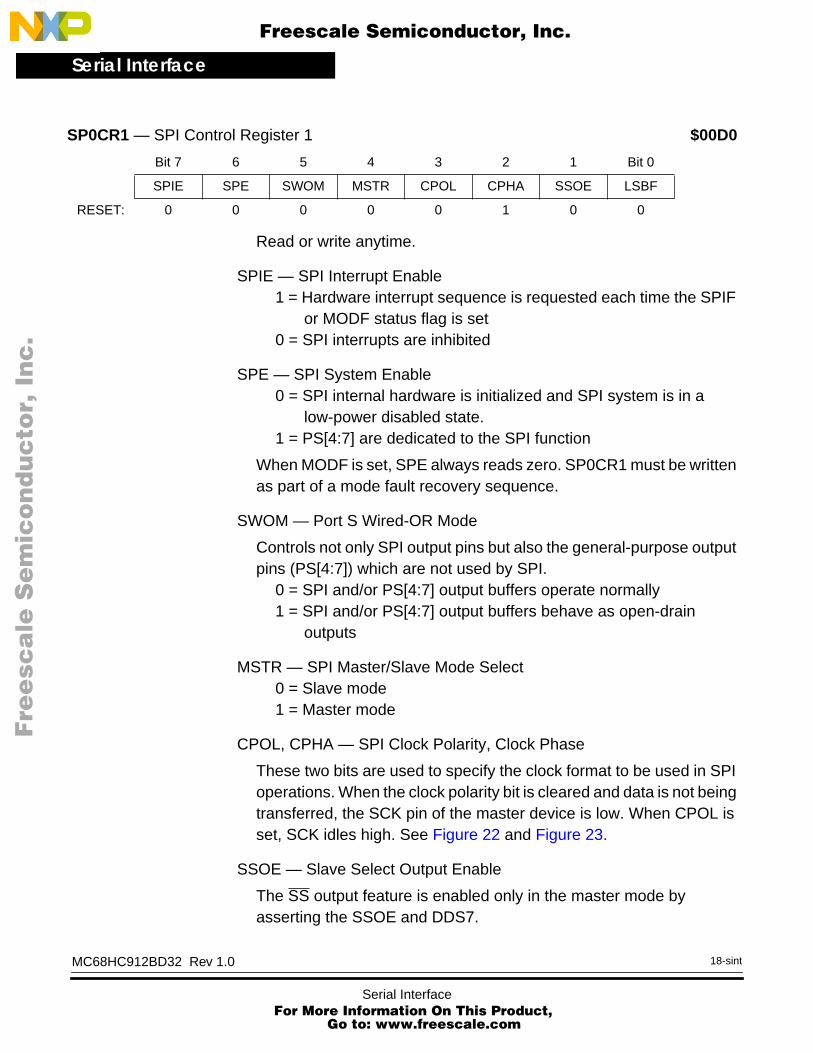
Serial Interface
F
ree
sca
le S
em
ico
nd
uc
tor,
I
Freescale Semiconductor, Inc.n
c..
.
Read or write anytime.
SPIE — SPI Interrupt Enable1 = Hardware interrupt sequence is requested each time the SPIF
or MODF status flag is set0 = SPI interrupts are inhibited
SPE — SPI System Enable0 = SPI internal hardware is initialized and SPI system is in a
low-power disabled state.1 = PS[4:7] are dedicated to the SPI function
When MODF is set, SPE always reads zero. SP0CR1 must be written as part of a mode fault recovery sequence.
SWOM — Port S Wired-OR Mode
Controls not only SPI output pins but also the general-purpose output pins (PS[4:7]) which are not used by SPI.
0 = SPI and/or PS[4:7] output buffers operate normally1 = SPI and/or PS[4:7] output buffers behave as open-drain
outputs
MSTR — SPI Master/Slave Mode Select0 = Slave mode1 = Master mode
CPOL, CPHA — SPI Clock Polarity, Clock Phase
These two bits are used to specify the clock format to be used in SPI operations. When the clock polarity bit is cleared and data is not being transferred, the SCK pin of the master device is low. When CPOL is set, SCK idles high. See Figure 22 and Figure 23.
SSOE — Slave Select Output Enable
The SS output feature is enabled only in the master mode by asserting the SSOE and DDS7.
SP0CR1 — SPI Control Register 1 $00D0
Bit 7 6 5 4 3 2 1 Bit 0
SPIE SPE SWOM MSTR CPOL CPHA SSOE LSBF
RESET: 0 0 0 0 0 1 0 0
MC68HC912BD32 Rev 1.0
Serial Interface For More Information On This Prod
Go to: www.freescale.com
18-sint
uct,
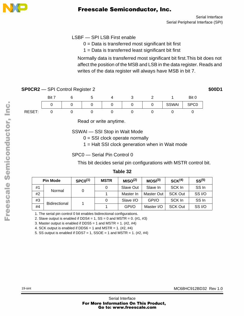
Serial InterfaceSerial Peripheral Interface (SPI)
MC68HC912BD32 Rev 1.0
F
ree
sca
le S
em
ico
nd
uc
tor,
I
Freescale Semiconductor, Inc.n
c..
.
19-sint
LSBF — SPI LSB First enable0 = Data is transferred most significant bit first1 = Data is transferred least significant bit first
Normally data is transferred most significant bit first.This bit does not affect the position of the MSB and LSB in the data register. Reads and writes of the data register will always have MSB in bit 7.
Read or write anytime.
SSWAI — SSI Stop in Wait Mode0 = SSI clock operate normally1 = Halt SSI clock generation when in Wait mode
SPC0 — Serial Pin Control 0
This bit decides serial pin configurations with MSTR control bit.
SP0CR2 — SPI Control Register 2 $00D1
Bit 7 6 5 4 3 2 1 Bit 0
0 0 0 0 0 0 SSWAI SPC0
RESET: 0 0 0 0 0 0 0 0
Table 32
Pin Mode SPC0(1) MSTR MISO(2) MOSI(3) SCK(4) SS(5)
#1Normal 0
0 Slave Out Slave In SCK In SS In
#2 1 Master In Master Out SCK Out SS I/O
#3Bidirectional 1
0 Slave I/O GPI/O SCK In SS In
#4 1 GPI/O Master I/O SCK Out SS I/O
1. The serial pin control 0 bit enables bidirectional configurations.2. Slave output is enabled if DDS4 = 1, SS = 0 and MSTR = 0. (#1, #3)3. Master output is enabled if DDS5 = 1 and MSTR = 1. (#2, #4)4. SCK output is enabled if DDS6 = 1 and MSTR = 1. (#2, #4)5. SS output is enabled if DDS7 = 1, SSOE = 1 and MSTR = 1. (#2, #4)
Serial Interface For More Information On This Product,
Go to: www.freescale.com
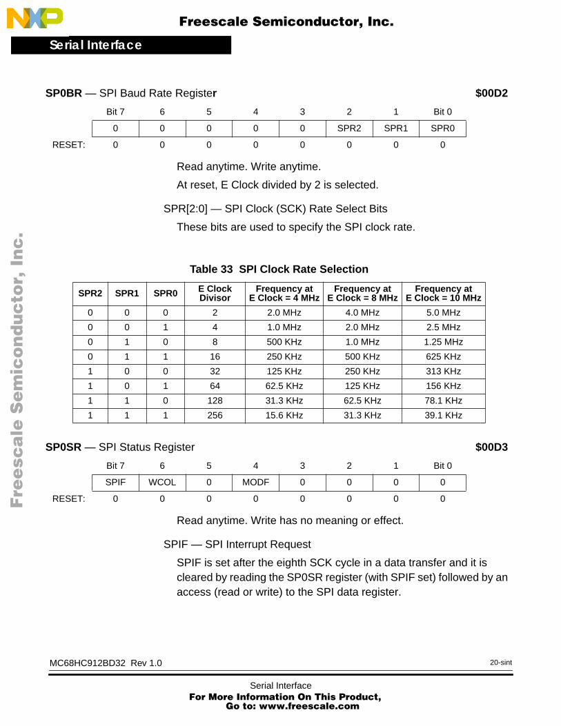
Serial Interface
F
ree
sca
le S
em
ico
nd
uc
tor,
I
Freescale Semiconductor, Inc.n
c..
.
Read anytime. Write anytime.
At reset, E Clock divided by 2 is selected.
SPR[2:0] — SPI Clock (SCK) Rate Select Bits
These bits are used to specify the SPI clock rate.
Read anytime. Write has no meaning or effect.
SPIF — SPI Interrupt Request
SPIF is set after the eighth SCK cycle in a data transfer and it is cleared by reading the SP0SR register (with SPIF set) followed by an access (read or write) to the SPI data register.
SP0BR — SPI Baud Rate Register $00D2
Bit 7 6 5 4 3 2 1 Bit 0
0 0 0 0 0 SPR2 SPR1 SPR0
RESET: 0 0 0 0 0 0 0 0
Table 33 SPI Clock Rate Selection
SPR2 SPR1 SPR0 E ClockDivisor
Frequency at E Clock = 4 MHz
Frequency at E Clock = 8 MHz
Frequency at E Clock = 10 MHz
0 0 0 2 2.0 MHz 4.0 MHz 5.0 MHz
0 0 1 4 1.0 MHz 2.0 MHz 2.5 MHz
0 1 0 8 500 KHz 1.0 MHz 1.25 MHz
0 1 1 16 250 KHz 500 KHz 625 KHz
1 0 0 32 125 KHz 250 KHz 313 KHz
1 0 1 64 62.5 KHz 125 KHz 156 KHz
1 1 0 128 31.3 KHz 62.5 KHz 78.1 KHz
1 1 1 256 15.6 KHz 31.3 KHz 39.1 KHz
SP0SR — SPI Status Register $00D3
Bit 7 6 5 4 3 2 1 Bit 0
SPIF WCOL 0 MODF 0 0 0 0
RESET: 0 0 0 0 0 0 0 0
MC68HC912BD32 Rev 1.0
Serial Interface For More Information On This Prod
Go to: www.freescale.com
20-sint
uct,

Serial InterfaceSerial Peripheral Interface (SPI)
MC68HC912BD32 Rev 1.0
F
ree
sca
le S
em
ico
nd
uc
tor,
I
Freescale Semiconductor, Inc.n
c..
.
21-sint
WCOL — Write Collision Status Flag
The MCU write is disabled to avoid writing over the data being transferred. No interrupt is generated because the error status flag can be read upon completion of the transfer that was in progress at the time of the error. Automatically cleared by a read of the SP0SR (with WCOL set) followed by an access (read or write) to the SP0DR register.
0 = No write collision1 = Indicates that a serial transfer was in progress when the MCU
tried to write new data into the SP0DR data register.
MODF — SPI Mode Error Interrupt Status Flag
This bit is set automatically by SPI hardware if the MSTR control bit is set and the slave select input pin becomes zero. This condition is not permitted in normal operation. In the case where DDRS bit 7 is set, the PS7 pin is a general-purpose output pin or SS output pin rather than being dedicated as the SS input for the SPI system. In this special case the mode fault function is inhibited and MODF remains cleared. This flag is automatically cleared by a read of the SP0SR (with MODF set) followed by a write to the SP0CR1 register.
Read anytime (normally only after SPIF flag set). Write anytime (see WCOL write collision flag).
Reset does not affect this address.
This 8-bit register is both the input and output register for SPI data. Reads of this register are double buffered but writes cause data to written directly into the serial shifter. In the SPI system the 8-bit data register in the master and the 8-bit data register in the slave are linked by the MOSI and MISO wires to form a distributed 16-bit register. When a data transfer operation is performed, this 16-bit register is serially shifted eight bit positions by the SCK clock from the master so the data is effectively exchanged between the master and the slave.
SP0DR — SPI Data Register $00D5
Bit 7 6 5 4 3 2 1 Bit 0
Bit 7 6 5 4 3 2 1 Bit 0
RESET: 0 0 0 0 0 0 0 0
Serial Interface For More Information On This Product,
Go to: www.freescale.com

Serial Interface
F
ree
sca
le S
em
ico
nd
uc
tor,
I
Freescale Semiconductor, Inc.n
c..
.
Note that some slave devices are very simple and either accept data from the master without returning data to the master or pass data to the master without requiring data from the master.
Port S
In all modes, port S bits PS[7:0] can be used for either general-purpose I/O, or with the SCI and SPI subsystems. During reset, port S pins are configured as high-impedance inputs (DDRS is cleared).
PORTS can be read anytime. When configured as an input, a read will return the pin level. When configured as output, a read will return the latched output data. Writes do not change pin state when pin configured for SPI or SCI output.
After reset all bits are configured as general-purpose inputs.
Port S shares function with the on-chip serial systems (SPI0 and SCI0).
Read or write anytime.
After reset, all general-purpose I/O are configured for input only.0 = Configure the corresponding I/O pin for input only1 = Configure the corresponding I/O pin for output
PORTS — Port S Data Register $00D6
Bit 7 6 5 4 3 2 1 Bit 0
PS7 PS6 PS5 PS4 PS3 PS2 PS1 PS0
PinFunction
SSCS
SCKMOSIMOMI
MISOSISO
I/O I/O TXD0 RXD0
DDRS — Data Direction Register for Port S $00D7
Bit 7 6 5 4 3 2 1 Bit 0
DDS7 DDS6 DDS5 DDS4 DDS3 DDS2 DDS1 DDS0
RESET: 0 0 0 0 0 0 0 0
MC68HC912BD32 Rev 1.0
Serial Interface For More Information On This Prod
Go to: www.freescale.com
22-sint
uct,

Serial InterfacePort S
MC68HC912BD32 Rev 1.0
F
ree
sca
le S
em
ico
nd
uc
tor,
I
Freescale Semiconductor, Inc.n
c..
.
23-sint
DDS0 — Data Direction for Port S, Bit 0
If the SCI receiver is configured for two-wire SCI operation, corresponding port S pins will be input regardless of the state of these bits.
DDS1 — Data Direction for Port S, Bit 1
If the SCI transmitter is configured for two-wire SCI operation, corresponding port S pins will be output regardless of the state of these bits.
DDS[2:3] — Data Direction for Port S Bit 2 and Bit 3
These bits are for general purpose I/O only.
DDS[6:4] — Data Direction for Port S Bits 6 through 4
If the SPI is enabled and expects the corresponding port S pin to be an input, it will be an input regardless of the state of the DDRS bit. If the SPI is enabled and expects the bit to be an output, it will be an output only if the DDRS bit is set.
DDS7 — Data Direction for Port S Bit 7
In SPI slave mode, DDS7 has no meaning or effect; the PS7 pin is dedicated as the SS input. In SPI master mode, DDS7 determines whether PS7 is an error detect input to the SPI or a general-purpose or slave select output line.
Read or write anytime.
RDPS2 — Reduce Drive of PS[7:4]0 = Port S output drivers for bits 7 through 4 operate normally.1 = Port S output pins for bits 7 through 4 have reduced drive
capability for lower power and less noise.
PURDS — Pullup and Reduced Drive for Port S $00DB
Bit 7 6 5 4 3 2 1 Bit 0
0 RDPS2 RDPS1 RDPS0 0 PUPS2 PUPS1 PUPS0
RESET: 0 0 0 0 0 0 0 0
Serial Interface For More Information On This Product,
Go to: www.freescale.com

Serial Interface
F
ree
sca
le S
em
ico
nd
uc
tor,
I
Freescale Semiconductor, Inc.n
c..
.
RDPS1 — Reduce Drive of PS[3:2]0 = Port S output drivers for bits 3 and 2 operate normally.1 = Port S output pins for bits 3 and 2 have reduced drive capability
for lower power and less noise.
RDPS0 — Reduce Drive of PS[1:0]0 = Port S output drivers for bits 1 and 0 operate normally.1 = Port S output pins for bits 1 and 0 have reduced drive capability
for lower power and less noise.
PUPS2 — Pull-Up Port S Enable PS[7:4]0 = No internal pull-ups on port S bits 7 through 4.1 = Port S input pins for bits 7 through 4 have an active pull-up
device. If a pin is programmed as output, the pull-up device becomes inactive.
PUPS1 — Pull-Up Port S Enable PS[3:2]0 = No internal pull-ups on port S bits 3 and 2.1 = Port S input pins for bits 3 and 2 have an active pull-up device.
If a pin is programmed as output, the pull-up device becomes inactive.
PUPS0 — Pull-Up Port S Enable PS[1:0]0 = No internal pull-ups on port S bits 1 and 0.1 = Port S input pins for bits 1 and 0 have an active pull-up device.
If a pin is programmed as output, the pull-up device becomes inactive.
MC68HC912BD32 Rev 1.0
Serial Interface For More Information On This Prod
Go to: www.freescale.com
24-sint
uct,

F
ree
sca
le S
em
ico
nd
uc
tor,
IFreescale Semiconductor, Inc.
nc
...
Byteflight™ ModuleByteflight™ Module
Contents
Introduction . . . . . . . . . . . . . . . . . . . . . . . . . . . . . . . . . . . . . . . . . . . . 167Features . . . . . . . . . . . . . . . . . . . . . . . . . . . . . . . . . . . . . . . . . . . . . . 168External Pins . . . . . . . . . . . . . . . . . . . . . . . . . . . . . . . . . . . . . . . . . . . 169Byteflight™ System. . . . . . . . . . . . . . . . . . . . . . . . . . . . . . . . . . . . . . 169Byteflight™ Protocol . . . . . . . . . . . . . . . . . . . . . . . . . . . . . . . . . . . . . 171Functional Overview . . . . . . . . . . . . . . . . . . . . . . . . . . . . . . . . . . . . . 176Low Power Modes. . . . . . . . . . . . . . . . . . . . . . . . . . . . . . . . . . . . . . . 186Programmer’s Model. . . . . . . . . . . . . . . . . . . . . . . . . . . . . . . . . . . . . 189Initialization . . . . . . . . . . . . . . . . . . . . . . . . . . . . . . . . . . . . . . . . . . . . 216FIFO Usage. . . . . . . . . . . . . . . . . . . . . . . . . . . . . . . . . . . . . . . . . . . . 217
Introduction
The serial bus interface module is the specific implementation of the BMW Byteflight™ concept targeted for the Motorola M68HC12 microcontroller family.
For the BMW Byteflight™ specification and related matters refer to the following documents:
BMW – Lastenheft SI-BUS , Ident-Nr.: LH 8 385 743.4ELMOS E100.34 S/E-Module, Rev. 02
MC68HC912BD32 Rev 1.0
1-sibusByteflight™ Module For More Information On This Product,
Go to: www.freescale.com
Byteflight™ Module
F
ree
sca
le S
em
ico
nd
uc
tor,
I
Freescale Semiconductor, Inc.n
c..
.
Features
The basic features of the Serial Bus Interface are as follows:
• Modular Architecture.
• Implementation of the BMW Byteflight™ protocol.
– 1 byte identifier.
– 1 byte data length field (4 bits length, 4 bits reserved).
– 0–12 bytes data.
– 2 bytes checksum, hardware CRC generation and checking.
– bit rate 10 Mbps.
– no collision on the bus.
– non-return-to-zero (NRZ) format.
• Double buffered receive storage scheme.
• 16 Message Buffers of 0–12 bytes data length.
• Programmable Message Buffer Configuration (transmit, receive, FIFO).
• Content-related addressing.
• Receive FIFO for bus monitoring with programmable acceptance filter.
• 11 maskable interrupt sources, generating five CPU interrupt vectors.
• Programmable bus master function.
• Programmable wake-up function.
• Low power sleep mode.
MC68HC912BD32 Rev 1.0
Byteflight™ Module For More Information On This Prod
Go to: www.freescale.com
2-sibus
uct,

Byteflight™ ModuleExternal Pins
F
ree
sca
le S
em
ico
nd
uc
tor,
I
Freescale Semiconductor, Inc.n
c..
.
External Pins
The serial bus interface module uses 2 external pins, 1 input (Rx) and 1 output (Tx).
Rx is on bit 0 of Port SBI, Tx is on bit 1. The remaining six signals of Port SBI are controlled by registers in the Byteflight™ address map
NOTE: Depending on the chip package, not all Port SBI signals may be available.
Byteflight™ System
A typical Byteflight™ system with the serial bus interface is shown in Figure 25 below.
MC68HC912BD32 Rev 1.0
3-sibusByteflight™ Module For More Information On This Product,
Go to: www.freescale.com
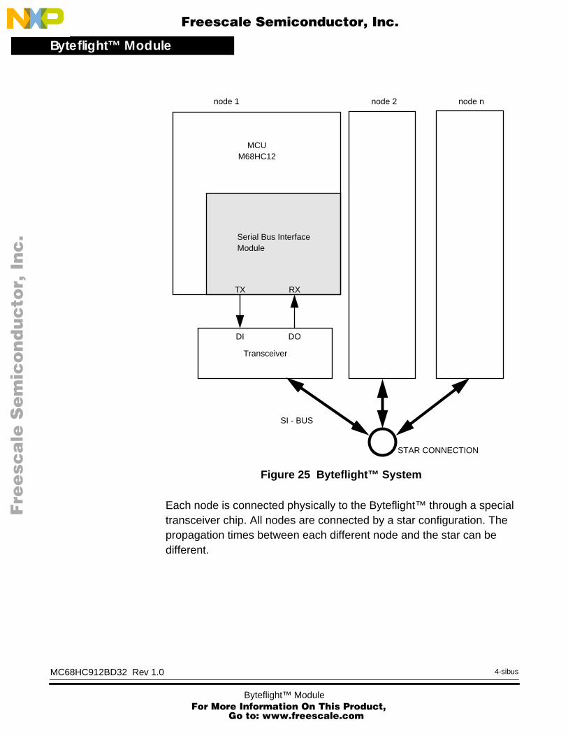
Byteflight™ Module
F
ree
sca
le S
em
ico
nd
uc
tor,
I
Freescale Semiconductor, Inc.n
c..
.
Figure 25 Byteflight™ System
Each node is connected physically to the Byteflight™ through a special transceiver chip. All nodes are connected by a star configuration. The propagation times between each different node and the star can be different.
SI - BUS
Serial Bus Interface
node 1 node 2 node n
TX RX
MCUM68HC12
Module
STAR CONNECTION
DI DO
Transceiver
MC68HC912BD32 Rev 1.0
Byteflight™ Module For More Information On This Prod
Go to: www.freescale.com
4-sibus
uct,

Byteflight™ ModuleByteflight™ Protocol
F
ree
sca
le S
em
ico
nd
uc
tor,
I
Freescale Semiconductor, Inc.n
c..
.
Byteflight™ Protocol
Byteflight™ Format and Timing
The BMW Byteflight™ protocol defines the message format, as follows:
Figure 26 Byteflight™ Message Format
The identifier (ID) byte is followed by the length (LEN) byte, which contains the number of data bytes (0..12) of the message. Following the data bytes (DATAn) are two CRC bytes (CRCH,CRCL), which contain the checksum. The value zero is not allowed for any identifier (ID). The priority of an identifier is inversely proportional to its value.
Figure 27 Byteflight™ Byte Format
One byte of a message is embedded into a start bit (‘1’) and a stop bit (‘0’), which are synchronization symbols and distinguish a message from a SYNC pulse. The transfer starts with the MSB first. The dominant state is represented by a logical ‘0’ and the recessive state is represented by a logical ‘1’.
Figure 28 Byteflight™ Message Start Sequence
IDLE ID LEN DATAn CRCH CRCL IDLE
1# BYTES: 1 1 10...12
START MSB
ONE BYTE FRAME
STOPLSB
t_bit
START MSB
ONE BYTE FRAME
STOPLSBIDLE
MESSAGE STARTSEQUENCE
MC68HC912BD32 Rev 1.0
5-sibusByteflight™ Module For More Information On This Product,
Go to: www.freescale.com
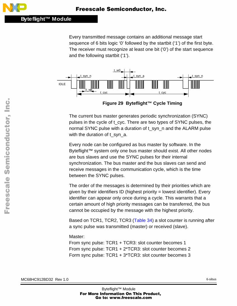
Byteflight™ Module
F
ree
sca
le S
em
ico
nd
uc
tor,
I
Freescale Semiconductor, Inc.n
c..
.
Every transmitted message contains an additional message start sequence of 6 bits logic ‘0’ followed by the startbit (‘1’) of the first byte. The receiver must recognize at least one bit (‘0’) of the start sequence and the following startbit (‘1’).
Figure 29 Byteflight™ Cycle Timing
The current bus master generates periodic synchronization (SYNC) pulses in the cycle of t_cyc. There are two types of SYNC pulses, the normal SYNC pulse with a duration of t_syn_n and the ALARM pulse with the duration of t_syn_a.
Every node can be configured as bus master by software. In the Byteflight™ system only one bus master should exist. All other nodes are bus slaves and use the SYNC pulses for their internal synchronization. The bus master and the bus slaves can send and receive messages in the communication cycle, which is the time between the SYNC pulses.
The order of the messages is determined by their priorities which are given by their identifiers ID (highest priority = lowest identifier). Every identifier can appear only once during a cycle. This warrants that a certain amount of high priority messages can be transferred, the bus cannot be occupied by the message with the highest priority.
Based on TCR1, TCR2, TCR3 (Table 34) a slot counter is running after a sync pulse was transmitted (master) or received (slave).
Master:From sync pulse: TCR1 + TCR3: slot counter becomes 1From sync pulse: TCR1 + 2*TCR3: slot counter becomes 2Form sync pulse: TCR1 + 3*TCR3: slot counter becomes 3
IDLE
t_cyc t_cyc
t_syn_n t_syn_a
t_w0
t_syn_n
t_wx
MC68HC912BD32 Rev 1.0
Byteflight™ Module For More Information On This Prod
Go to: www.freescale.com
6-sibus
uct,

Byteflight™ ModuleByteflight™ Protocol
MC68HC912BD32 Rev 1.0
F
ree
sca
le S
em
ico
nd
uc
tor,
I
Freescale Semiconductor, Inc.n
c..
.
7-sibus
Slave:From sync pulse: TCR2 + TCR3: slot counter becomes 1From sync pulse: TCR2 + 2*TCR3: slot counter becomes 2Form sync pulse: TCR2 + 3*TCR3: slot counter becomes 3
When a node wants to transmit e.g. ID=2 and the slot counter reaches the value 2, the node starts to transmit and stops the slot counter. All other nodes receive that message in time slot = 2 and also stop their slot counters as soon as they detect bus activity. When a rising edge (e.g. end of message) on the bus is detected the wait time is calculated again, i.e. the slot counter is incremented again after TCR1+TCR3 (last bus activity was transmitted) or TCR2+TCR3 (last bus activity was received):
Assuming that a message with ID = 2 was received or transmitted in the time slot = 2 the slot counter is restarted in the following way:
Last bus activity was transmitted:Waiting from rising edge: TCR1 + TCR3: slot counter is incremented by one.TCR3 later: slot counter is incremented again.
Last bus activity was received:Waiting from rising edge: TCR12+ TCR3: slot counter is incremented by one.TCR3 later: slot counter is incremented again.
Cyclic Redundancy Check c(CRC)
Every message transmitted onto a Byteflight™ network contains two CRC bytes for error detection. These two bytes are produced by shifting the ID, LEN and DATA bytes through a preset series of feedback shift registers (For more details refer to BMW – Lastenheft SI-Bus). The 15-bit CRC result is appended to the message following the data portion. The byte CRCH contains the upper 8 bits of the CRC result, the byte CRCL contains the lower 7 bits, the LSB of CRCL is set to ‘0’.
Any node which receives the message recalculates the CRC value with the same hardware and compares bytewise the result against the received CRC value. In the case of a mismatch a CRC Error is detected.
Byteflight™ Module For More Information On This Product,
Go to: www.freescale.com

Byteflight™ Module
F
ree
sca
le S
em
ico
nd
uc
tor,
I
Freescale Semiconductor, Inc.n
c..
.
Byteflight™ Timing Parameters
Table 34 Parameter of the Byteflight™ System
Symbol Characteristic Description Typ
t_bit bit timetime for the transmission of one bit, defined by the physical limitations of the system
100 ns
t_cyc cycle time (note 2) time distance between the end of the SYNC pulses 250 µs(1)
t_cyc_min min cycle time min time distance between the end of the SYNC pulses
249.725µs
t_cyc_max max cycle time max time distance between the end of the SYNC pulses
250.275µs
t_maxmaximum run time of a signal in the bus system
max run time of a signal between a transmit module and the recognition by a receive module
tbd,ca 400ns
t_tolerancetolerance of the run time of a signal in the bus system
is the sum of all tolerances tbd,ca 300ns
t_idle_min min bus idle timemin bus idle time between two messages or the SYNC pulse and a message
11 * t_bit
t_syn_a Sync pulse ALARM duration of the Sync pulse in the case of ALARM 2 µs(2)
t_syn_a_minSync pulse ALARM, min pulse width
min duration of the Sync pulse in the case of ALARM 1.85 µs
t_syn_a_maxSync pulse ALARM, max pulse width
max duration of the Sync pulse in the case of ALARM
2.15 µs
t_syn_n Sync pulse NORMAL duration of the Sync pulse in the normal case 3 µs(3)
t_syn_n_minSync pulse NORMAL, min pulse width
min duration of the Sync pulse in the normal case 2.85 µs
t_syn_n_maxSync pulse NORMAL, max pulse width
max duration of the Sync pulse in the normal case 3.15 µs
t_w0 Sync pulse wait timeminimum time between end of a message and end of SYNC pulse, t_w0 >= t_idle_min + t_syn_n_max
< 6000ns
ID Identifier allowed values between 1 .. 255
IDx-1 previous IdentifierIdentifier of the previously received or transmitted message. When the Sync pulse was the last activity on the bus, then IDx-1 = 0
MC68HC912BD32 Rev 1.0
Byteflight™ Module For More Information On This Prod
Go to: www.freescale.com
8-sibus
uct,

Byteflight™ ModuleByteflight™ Protocol
MC68HC912BD32 Rev 1.0
F
ree
sca
le S
em
ico
nd
uc
tor,
I
Freescale Semiconductor, Inc.n
c..
.
9-sibus
t_wx message idle time
time between the end of the Sync pulse or end of the previous message and the start of the transmitted message. t_wx >= t_idle_min
t_wx = twx0_tx + twx_delta * (ID - IDx-1), when the node sent the last activity on the bus
t_wx = twx0_rx + twx_delta * (ID - IDx-1), when the node received the last activity on the bus
t_wx0_txconstant part of t_wx when last bus activity was transmitted
t_wx0_tx can be programmed individually for each node in the register TCR1
<1900ns
t_wx0_rxconstant part of t_wx when last bus activity was received
t_wx0_rx can be programmed individually for each node in the register TCR2
<1900ns
t_latest_tx latest start of transmit t_latest_tx is currently hard wired 229.0 µs
t_start_seq_tx length of tx start sequence t_start_seq_tx is currently hard wired 600ns
t_start_seq_rxlength of rx start sequence (max)
t_start_seq_rx is currently hard wired 975ns
t_start_seq_rxlength of rx start sequence (min)
t_start_seq_rx is currently hard wired 100ns
t_wx_delta multiplier part of t_wxthis value must be assigned identically for each node using register TCR3. t_wx_delta = t_max + t_tolerance
< 1200ns> 200ns
t_recognizerecognition time for bus activity
time required for recognition of bus activity: time from falling edge of RX pin until the bus controller can stop a waiting transmit process
<125ns
t_wake_up length of wake up pulsea sequence of dominant and recessive pulses of length t_wake_up is sent out if WPULSE is set
6.4 µs
1. 249.75µs<=t_cyc<=250.25µs in 100% of cases there is no error, t_cyc<249.7µs or t>250.3µs in 100% of cases sync tooearly/ lost
2. 1.875µs<=t_syn_a<=2.125µs in 100% of cases sync alarm is accepted, t_syn_a<1.825µs or t_syn_a>2.175µs in 100% ofsync alarm is not accepted, but illegal pulse is detected
3. 2.875µs<=t_syn_n<=3.125µs in 100% of cases sync normal is accepted, t_syn_n<2.825µs or t_syn_n>3.175µs in 100%of sync normal is not accepted, but illegal pulse is detected
Table 34 Parameter of the Byteflight™ System
Symbol Characteristic Description Typ
Byteflight™ Module For More Information On This Product,
Go to: www.freescale.com

Byteflight™ Module
F
ree
sca
le S
em
ico
nd
uc
tor,
I
Freescale Semiconductor, Inc.n
c..
.
Tolerances The receiver is designed to handle signals on the Byteflight™ with the tolerances shown in Figure 30 and in Table 35.
Figure 30 Pulse Time Tolerance
Glitch Filtering Glitches of a duration less than 25ns are filtered out.
Functional Overview
Recieve Process A part or all of the message buffers can be configured as a mailbox system consisting of dedicated receive buffers. The mailbox must be contiguous in the register map starting after the last FIFO buffer and ending before the first transmit buffer. The Byteflight™ transfers received messages from the serial message buffer to the mailbox message buffer with matching ID.
RX PIN
trr
RX PIN
tff
trf
tfr
Table 35 Tolerances
Tolerance Range
trr n * t_bit ± 5ns 2 ≤ n ≤ 10
tff n * t_bit ± 5ns 2 ≤ n ≤ 10
trf n * t_bit ± 35ns 1 ≤ n ≤ 10
tfr n * t_bit ± 35ns 1 ≤ n ≤ 10
MC68HC912BD32 Rev 1.0
Byteflight™ Module For More Information On This Prod
Go to: www.freescale.com
10-sibus
uct,

Byteflight™ ModuleFunctional Overview
MC68HC912BD32 Rev 1.0
F
ree
sca
le S
em
ico
nd
uc
tor,
I
Freescale Semiconductor, Inc.n
c..
.
11-sibus
To prepare or change a message buffer for reception the following steps in soft reset mode are required:
• Lock the corresponding message buffer in order to appear in the Active Receive Buffer window in the memory map.
• Wait for lock acknowledge.
• Write the matching ID to this Active Receive Buffer.
• Clear the IFLG (buffer empty) by writing a ‘1’ to it.
NOTE: It is recommended to split clearing of the IFLG and unlocking the message buffer into two separate instructions, i.e. clear the IFLG and then unlock the buffer.
Once these steps are performed, the message buffer functions as an active receive buffer and participates in the internal matching process, which takes place every time the Byteflight™ receives a message. In this process, all active receive buffers compare their ID value to the newly received one. The buffer matching the received ID will be updated with the new message at the end of reception if the buffer is not locked. The matching buffer will be overwritten if the buffer was already full (IFLG = 1). The matching buffer will not be updated if it is still locked. The buffer will be updated as soon as it is unlocked. If the buffer is locked for more than one cycle and if the same ID is received twice during this period, the buffer will be updated with the newer message as soon as it is unlocked.
The corresponding IFLG flag (buffer full) is set every time the buffer is updated, and if enabled a receive interrupt is generated. Erroneous messages will be ignored and will not overwrite unlocked full buffers. Only unique IDs must be used. ID ‘0’ should be used to deactivate a receive buffer.
To read a receive message buffer the following steps are required:
• Lock the corresponding message buffer in order to appear in the Active Receive Buffer window in the memory map.
• Wait for lock acknowledge.
• Read the Active Receive Buffer.
Byteflight™ Module For More Information On This Product,
Go to: www.freescale.com

Byteflight™ Module
F
ree
sca
le S
em
ico
nd
uc
tor,
I
Freescale Semiconductor, Inc.n
c..
.
• Clear the IFLG (buffer empty) by writing a ‘1’ to it.
• Unlock the message buffer.
NOTE: Bit manipulation instructions (BSET or BCLR) shall not be used to clear interrupt flags.
Receive FIFO Function
A part or all of the message buffers can be configured to a Receive First-In-First-Out (FIFO) System, which can be used as logic analyzer buffers or for receiving consecutive data streams.
The FIFO starts with message buffer 0 and can be configured to the maximum of all 16 message buffers. Every incoming message not matching with any receive identifier but matching the programmable FIFO filter is stored into the FIFO buffer system. A status bit shows that the Receive FIFO is not empty, another status bit shows that a Receive FIFO Overrun has been detected. If enabled, interrupts are generated.
There are two index registers associated with the FIFO. The PUT Index Register (PUTIDX) is used as an index to the next available location in the FIFO buffer system. When a new message has been received it is written into the buffer addressed by the PUTIDX; the PUTIDX is then incremented so it addresses the next buffer. If the PUTIDX is incremented past the highest FIFO message buffer the PUTIDX is reset to 0. The GET Index Register (GETIDX) is used to address the next FIFO buffer to be read. The GETIDX is incremented when unlocking the Receive FIFO buffer. The FIFO buffer system is completely filled, when the PUT Pointer (PUTIDX) has reached again the value of the GET Pointer (GETIDX). A new incoming messages cannot be stored into the FIFO. The FIFO overrun flag is set at the end of this message if no error has occurred. A Receive FIFO non empty status is detected when the PUTIDX differs from the GETIDX. This indicates there is at least one received message in the FIFO buffer system. The PUTIDX and the GETIDX are not addressable by the CPU.
The FIFO empty, FIFO not empty and the FIFO overrun situations are explained in Figure 31 below for a three buffer FIFO.
MC68HC912BD32 Rev 1.0
Byteflight™ Module For More Information On This Prod
Go to: www.freescale.com
12-sibus
uct,

Byteflight™ ModuleFunctional Overview
MC68HC912BD32 Rev 1.0
F
ree
sca
le S
em
ico
nd
uc
tor,
I
Freescale Semiconductor, Inc.n
c..
.
13-sibus
Figure 31 FIFO Status (empty, not empty, overrun) - Example with 3 buffers
To read a Receive FIFO buffer the FIFO must be locked by setting the LOCK bit of buffer 0. The message buffer addressed by GETIDX appears in the Active Receive FIFO Buffer window in the memory map. After reading the FIFO must be unlocked and the GETIDX will be incremented.
There is a programmable identifier acceptance filter for the Receive FIFO system. The FIFO identifier acceptance register (FIDAC) defines the acceptable pattern of the identifier to be received. The FIFO identifier mask register (FIDMR) specifies which of the corresponding bits are marked ‘don’t care’ for acceptance filtering.
There is also a programmable identifier rejection filter for the Receive FIFO system. The FIFO identifier rejection register (FIDRJ) defines the acceptable pattern of the identifier to be rejected. The FIFO identifier rejection mask register (FIDRMR) specifies which of the corresponding bits are marked ‘don’t care’ for rejection filtering.
If acceptance and rejection filter are configured to match the same identifier, the message will be rejected.
GETIDX(READ)
0 1 2
A - -MESSAGES:
PUTIDX(WRITE)
FIFO NOT EMPTY
BUFFERS:
GETIDX(READ)
0 1 2
A B CMESSAGES:
PUTIDX(WRITE)
FIFO OVERRUN
BUFFERS:
PUTIDX WAS INCREMENTED LAST + NEW INCOMING MESSAGE (WHICH
GETIDX(READ)
0 1 2
- - -MESSAGES:
PUTIDX(WRITE)
FIFO EMPTY
BUFFERS:
IS LOST)
Byteflight™ Module For More Information On This Product,
Go to: www.freescale.com

Byteflight™ Module
F
ree
sca
le S
em
ico
nd
uc
tor,
I
Freescale Semiconductor, Inc.n
c..
.
Transmit Process A part or all of the message buffers can be configured as transmit buffers. The set of transmit buffers must be contiguous in the register map starting at buffer 15 and ending before the first receive buffer. A message is submitted for transmission by unlocking the corresponding non-empty (IFLG = 0) transmit buffer. The transmit buffer remains active until the message is transmitted or aborted.
If there are several messages pending for transmission within the interface, the message with the highest priority (lowest identifier) is selected next. Only transmit buffers which were unlocked and full before a sync pulse are transmitted in the following cycle. If there are two or more transmit buffers with the same identifier, the buffer with the lowest address wins the internal arbitration and will be transmitted, the remaining buffer(s) with the same ID will be removed from the arbitration process until the next communication cycle. A full buffer can be aborted by setting the corresponding abort request bit. At the next sync pulse the interrupt status flag (buffer is empty) and the abort acknowledge flag are set if the buffer has been aborted. Only the interrupt status flag is set if the buffer has been sent out.
Table 36 Acceptance/rejection filter mechanism - Examples
Example 1 (1)
1. All registers in reset state: Do not accept any valid system ID ($01...$FF).
Example 2 (2)
2. Acceptance and rejection filter set to match same ID: Do not accept ID’s other than $55,then reject $55.
Example 3 (3)
3. Accept all ID’s ($00 no valid system ID), then reject all ID’s with high nibble=0.
Example 4 (4)
4. Do not accept ID’s $80 to $FF, accept all $00 to $7F ($00 no valid system ID), then rejectall ID’s with bit 4 and 5 set.
FIDAR $00 $55 $xx %0xxx xxxx
FIDMR $00 $00 $FF %0111 1111
FIDRJ $xx $55 $0x %xx11 xxxx
FIDRMR $FF $00 $0F %1100 1111
Stage I: Accept ID $00 $55 $00...$FF $00...$7F
Stage II: Reject ID none $55 $00...$0F$30...$3F$70...$7F
Receive ID $00 none $10...$FF$00...$2F$40...$6F
MC68HC912BD32 Rev 1.0
Byteflight™ Module For More Information On This Prod
Go to: www.freescale.com
14-sibus
uct,

Byteflight™ ModuleFunctional Overview
MC68HC912BD32 Rev 1.0
F
ree
sca
le S
em
ico
nd
uc
tor,
I
Freescale Semiconductor, Inc.n
c..
.
15-sibus
To prepare a transmit message buffer for transmission the following steps are required:
• Lock the corresponding message buffer in order to appear in the Active Transmit Buffer window in the memory map.
• Wait for lock acknowledge.
• Write to the Active Transmit Buffer (ID, LEN, DATA). If no update is needed, write is not required.
• Unlock the message buffer and clear the IFLG (buffer full) by writing a ‘1’ to it.
NOTE: Bit manipulation instructions (BSET or BCLR) shall not be used to clear interrupt flags.It is recommended to use one single instruction to clear the IFLG and to unlock the buffer.
Synchronization Process
The node can be configured as bus master. In this case the module generates the periodic synchronization (SYNC) pulses. If the ALARM bit is set, the master generates the ALARM pulses as long as this bit is asserted. The ALARM bit is reset after 255ms - 256ms if it has not been set again by the CPU within that period.
Byteflight™ Module For More Information On This Product,
Go to: www.freescale.com
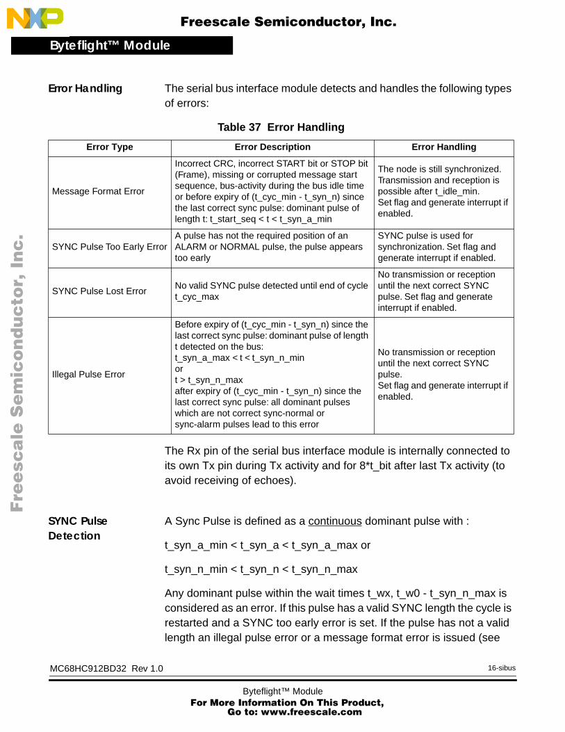
Byteflight™ Module
F
ree
sca
le S
em
ico
nd
uc
tor,
I
Freescale Semiconductor, Inc.n
c..
.
Error Handling The serial bus interface module detects and handles the following types of errors:
The Rx pin of the serial bus interface module is internally connected to its own Tx pin during Tx activity and for 8*t_bit after last Tx activity (to avoid receiving of echoes).
SYNC Pulse Detection
A Sync Pulse is defined as a continuous dominant pulse with :
t_syn_a_min < t_syn_a < t_syn_a_max or
t_syn_n_min < t_syn_n < t_syn_n_max
Any dominant pulse within the wait times t_wx, t_w0 - t_syn_n_max is considered as an error. If this pulse has a valid SYNC length the cycle is restarted and a SYNC too early error is set. If the pulse has not a valid length an illegal pulse error or a message format error is issued (see
Table 37 Error Handling
Error Type Error Description Error Handling
Message Format Error
Incorrect CRC, incorrect START bit or STOP bit (Frame), missing or corrupted message start sequence, bus-activity during the bus idle time or before expiry of (t_cyc_min - t_syn_n) since the last correct sync pulse: dominant pulse of length t: t_start_seq < t < t_syn_a_min
The node is still synchronized. Transmission and reception is possible after t_idle_min.Set flag and generate interrupt if enabled.
SYNC Pulse Too Early ErrorA pulse has not the required position of an ALARM or NORMAL pulse, the pulse appears too early
SYNC pulse is used for synchronization. Set flag and generate interrupt if enabled.
SYNC Pulse Lost ErrorNo valid SYNC pulse detected until end of cycle t_cyc_max
No transmission or reception until the next correct SYNC pulse. Set flag and generate interrupt if enabled.
Illegal Pulse Error
Before expiry of (t_cyc_min - t_syn_n) since the last correct sync pulse: dominant pulse of length t detected on the bus:t_syn_a_max < t < t_syn_n_minort > t_syn_n_maxafter expiry of (t_cyc_min - t_syn_n) since the last correct sync pulse: all dominant pulses which are not correct sync-normal or sync-alarm pulses lead to this error
No transmission or reception until the next correct SYNC pulse. Set flag and generate interrupt if enabled.
MC68HC912BD32 Rev 1.0
Byteflight™ Module For More Information On This Prod
Go to: www.freescale.com
16-sibus
uct,

Byteflight™ ModuleFunctional Overview
MC68HC912BD32 Rev 1.0
F
ree
sca
le S
em
ico
nd
uc
tor,
I
Freescale Semiconductor, Inc.n
c..
.
17-sibus
Table 37). A valid synchronization edge is detected if the pulse length is correct independent of the pulse position. If the pulse position is not correct either a pulse too early or a sync lost error condition is set. ALARM and NORMAL SYNC are distinguished only by the bits SYNAIF and SYNNIF.
Figure 32 SYNC Pulse Errors Detection
t_cyc
t_wx0 t_wxjt_wxi
>t_w0
VALID SYNC ALARM
INDICATES VALID SYNCHRONIZATION EDGE AND SETS SYNC-FLAG
VALID SYNC NORMAL
SYNC TOO EARLY
SYNC TOO EARLY & ALARM
SYNC LOST
t_syn_n
t_syn_n
t_syn_a
t_syn_a
t_syn_n
t_syn_a
ALARM
SYNC LOSTNOT A VALID SYNC LENGTH
SYNC LOST
PULSE ERROR
SYNC PULSE DETECT WINDOWS
SYNC NORMAL
SYNC ALARM
t_pulse
t_cyc_max
Byteflight™ Module For More Information On This Product,
Go to: www.freescale.com

Byteflight™ Module
F
ree
sca
le S
em
ico
nd
uc
tor,
I
Freescale Semiconductor, Inc.n
c..
.
Interrupts The Serial Bus Interface module is capable of generating five different interrupt requests (vectors) mapped onto different interrupt sources:
1. SYNC pulse interrupt at high priority (SYNC pulse NORMAL or ALARM received)
2. Receive FIFO not empty
3. Receive Interrupt
4. Synchronization Interrupt (SYNC pulse NORMAL or ALARM received)
5. General Interrupt (all errors, transmit and other interrupt sources)
– Transmit Interrupt
– Receive FIFO overrun
– Message Format Error (CRC Error, Frame Error)
– SYNC Pulse To Early Error
– SYNC Pulse Lost Error
– Illegal Pulse Error
– Wake-Up Interrupt
– Locking Error Interrupt
– Slot Mismatch Interrupt
MC68HC912BD32 Rev 1.0
Byteflight™ Module For More Information On This Prod
Go to: www.freescale.com
18-sibus
uct,
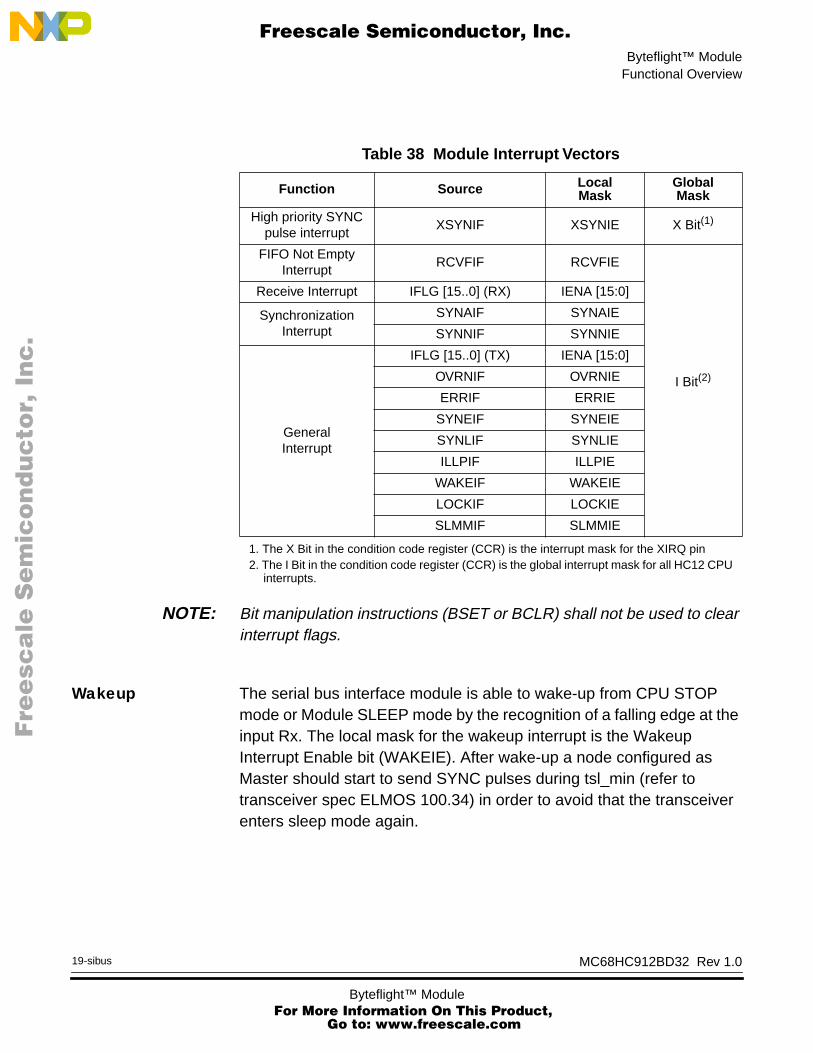
Byteflight™ ModuleFunctional Overview
MC68HC912BD32 Rev 1.0
F
ree
sca
le S
em
ico
nd
uc
tor,
I
Freescale Semiconductor, Inc.n
c..
.
19-sibus
NOTE: Bit manipulation instructions (BSET or BCLR) shall not be used to clear interrupt flags.
Wakeup The serial bus interface module is able to wake-up from CPU STOP mode or Module SLEEP mode by the recognition of a falling edge at the input Rx. The local mask for the wakeup interrupt is the Wakeup Interrupt Enable bit (WAKEIE). After wake-up a node configured as Master should start to send SYNC pulses during tsl_min (refer to transceiver spec ELMOS 100.34) in order to avoid that the transceiver enters sleep mode again.
Table 38 Module Interrupt Vectors
Function Source LocalMask
GlobalMask
High priority SYNC pulse interrupt
XSYNIF XSYNIE X Bit(1)
1. The X Bit in the condition code register (CCR) is the interrupt mask for the XIRQ pin
FIFO Not Empty Interrupt
RCVFIF RCVFIE
I Bit(2)
2. The I Bit in the condition code register (CCR) is the global interrupt mask for all HC12 CPUinterrupts.
Receive Interrupt IFLG [15..0] (RX) IENA [15:0]
Synchronization Interrupt
SYNAIF SYNAIE
SYNNIF SYNNIE
GeneralInterrupt
IFLG [15..0] (TX) IENA [15:0]
OVRNIF OVRNIE
ERRIF ERRIE
SYNEIF SYNEIE
SYNLIF SYNLIE
ILLPIF ILLPIE
WAKEIF WAKEIE
LOCKIF LOCKIE
SLMMIF SLMMIE
Byteflight™ Module For More Information On This Product,
Go to: www.freescale.com

Byteflight™ Module
F
ree
sca
le S
em
ico
nd
uc
tor,
I
Freescale Semiconductor, Inc.n
c..
.
Low Power Modes
In addition to normal mode, the Serial Bus Interface module has three modes with reduced power consumption: Sleep, Soft Reset and Power Save mode. In Sleep and Soft Reset mode, power consumption is reduced by stopping all clocks except those to access the register. In Power Save mode, all clocks are stopped and no power is consumed (except leakage current).
The WAI and STOP instruction put the MCU in low power consumption stand-by modes. Table 39 summarizes the combinations of Byteflight™ and CPU modes. A particular combination of modes is entered for the given settings of the bits SSWAI, SLPAK, and SFTRES. For all modes, an Byteflight™ wake-up interrupt can occur only if SLPAK=WAKEIE=1. While the CPU is in Wait mode, the Byteflight™ can be operated in normal mode and generate interrupts. Registers can still be accessed via background debug mode.
Table 39 Byteflight™ vs. CPU operating modes
Byteflight™ Mode
CPU Mode
STOP WAIT RUN
Power SaveSSWAI = X(1)
SLPAK = XSFTRES = X
1. ‘X’ means don’t care.
SSWAI = 1SLPAK = X
SFTRES = X
SleepSSWAI = 0SLPAK = 1
SFTRES = 0
SSWAI = XSLPAK = 1
SFTRES = 0
Soft ResetSSWAI = 0SLPAK = 0
SFTRES = 1
SSWAI = XSLPAK = 0
SFTRES = 1
NormalSSWAI = 0SLPAK = 0
SFTRES = 0
SSWAI = XSLPAK = 0
SFTRES = 0
MC68HC912BD32 Rev 1.0
Byteflight™ Module For More Information On This Prod
Go to: www.freescale.com
20-sibus
uct,

Byteflight™ ModuleLow Power Modes
MC68HC912BD32 Rev 1.0
F
ree
sca
le S
em
ico
nd
uc
tor,
I
Freescale Semiconductor, Inc.n
c..
.
21-sibus
Module Sleep Mode
The CPU can request the Byteflight™ to enter this low-power mode by asserting the SLPRQ bit in the Module Configuration Register. The time when the Byteflight™ enters Sleep Mode depends on its activity:
• if it is transmitting, it continues to transmit until there is no more message to be transmitted, and then goes into Sleep Mode.
• if it is receiving, it waits for the end of this message and then goes into Sleep Mode.
• if it is neither transmitting nor receiving, it immediately goes into Sleep Mode.
NOTE: The application software must avoid setting up a transmission (by clearing one or more IFLG flag(s)) and immediately request Sleep Mode (by setting SLPRQ). It then depends on the exact sequence of operations whether the Byteflight™ starts transmitting or goes into Sleep Mode directly. The application software should use SLPAK as a handshake indication for the request (SLPRQ) to go into Sleep Mode.
During Sleep Mode, the SLPAK flag is set. When in Sleep Mode, the Byteflight™ stops its internal clocks. However, clocks to allow register accesses still run. The Tx pin stays in recessive state. It is possible to access locked transmit and receive buffers but no message abort and buffer lock/unlock takes place while in sleep mode.
The Byteflight™ leaves Sleep Mode (wake-up) when
• bus activity occurs or
• the MCU clears the SLPRQ or
• the MCU sets SFTRES.
NOTE: The MCU cannot clear the SLPRQ bit before the Byteflight™ is in Sleep Mode (SLPAK = 1).
After wake-up, the Byteflight™ waits for a sync pulse to synchronize to the bus. As a consequence, if the Byteflight™ is woken-up by a valid message, this message is not received. The receive message buffer content is not affected by sleep-mode. All pending actions are executed upon wake-up: message aborts, buffer lock and message transmissions.
Byteflight™ Module For More Information On This Product,
Go to: www.freescale.com

Byteflight™ Module
F
ree
sca
le S
em
ico
nd
uc
tor,
I
Freescale Semiconductor, Inc.n
c..
.
CPU WAIT Mode The WAIT instruction places the MCU in the low-power consumption WAIT mode. Depends on the SSWAI-bit the module can be stopped or remains active during CPU wait mode. When SSWAI is cleared the module will stay synchronized to the Byteflight™ and can generate interrupts to the CPU if enabled. Any such interrupt will bring the MCU out of wait mode.
CPU STOP Mode A CPU STOP instruction stops the internal oscillator and halts all internal processing. The application software has to bring the module into the module sleep mode before the CPU STOP instruction is executed if the Byteflight™ has to wake up the CPU. The processor can be brought out of the STOP mode only by an external interrupt, RESET or WAKEUP interrupt of the module.
SOFT RESET Mode In Soft Reset Mode, the Byteflight™ module is stopped. Registers can still be accessed. This mode is used to initialize the module configuration.
When setting the SFTRES bit, the Byteflight™ module immediately stops all ongoing transmission and reception, potentially causing protocol violations. The user is required to take care that the Byteflight™ is not active when Soft Reset Mode is entered. The recommended procedure is to bring the Byteflight™ module into Sleep Mode before the SFTRES bit is set.
MC68HC912BD32 Rev 1.0
Byteflight™ Module For More Information On This Prod
Go to: www.freescale.com
22-sibus
uct,

Byteflight™ ModuleProgrammer’s Model
MC68HC912BD32 Rev 1.0
F
ree
sca
le S
em
ico
nd
uc
tor,
I
Freescale Semiconductor, Inc.n
c..
.
23-sibus
Programmer’s Model
This section describes the content and use of the registers in the serial bus interface module. An overview of all registers is shown in Figure 33.
There are three sets of registers which are accessible by the CPU:
• the general control registers,
• the 16 buffer control registers,
• and the 16 configurable message buffers with one 14 bytes active transmit buffer, one 14 bytes active receive buffer and one 14 bytes active receive FIFO buffer mirrored to the memory map.
16 of 18 message buffers are accessible by window scheme
$xx00 GENERAL CONTROL 32 BYTES
BUFFER 17 - 14 BYTES
$xx1F BUFFER 16 - 14 BYTES
$xx20 ACTIVE TRANSMIT BUFFER14 BYTES
LOCK BUFFER 15 - 14 BYTES ↓Transmit
assignment of buffers
⇐ PUTIDX
$xx2F
BUFFER 2 - 14 BYTESLOCK
$xx40 ACTIVE RECEIVE FIFO BUFFER14 BYTES
GETIDX BUFFER 1 - 14 BYTES↑Receive, FIFO
$xx4F BUFFER 0 - 14 BYTES
$xx50 BUFFER CONTROL16 BYTES$xx5F
Figure 33 Register Map
Byteflight™ Module For More Information On This Product,
Go to: www.freescale.com

Byteflight™ Module
F
ree
sca
le S
em
ico
nd
uc
tor,
I
Freescale Semiconductor, Inc.n
c..
.
Overview of All Registers
NOTE: All register bits marked by ‘*’ can be updated during soft reset only!
ADDR REGISTER R/W BIT 7 BIT 6 BIT 5 BIT 4 BIT 3 BIT 2 BIT 1 BIT 0
$xx00 MCRR
SFTRES MASTER* ALARMSLPAK
SLPRQ WPULSE* SSWAI0
W
$xx01 FSIZRR 0 0 0
FSIZ4* FSIZ3* FSIZ2* FSIZ1* FSIZ0*W
$xx02 TCR1R
TWX0T7* TWX0T6* TWX0T5* TWX0T4* TWX0T3* TWX0T2* TWX0T1* TWX0T0*W
$xx03 TCR2R
TWX0R7* TWX0R6* TWX0R5* TWX0R4* TWX0R3* TWX0R2* TWX0R1* TWX0R0*W
$xx04 TCR3R
TWXD7* TWXD6* TWXD5* TWXD4* TWXD3* TWXD2* TWXD1* TWXD0*W
$xx05 RESERVED FOR TESTR
W
$xx06 RISRR RCVFIF RXIF
SYNAIF SYNNIF SLMMIF0
XSYNIF OPTDFW
$xx07 GISRR TXIF
OVRNIF ERRIF SYNEIF SYNLIF ILLPIFLOCKIF
WAKEIFW
$xx08 RIERR
RCVFIE RXIE SYNAIE SYNNIE SLMMIE0
XSYNIE0
W
$xx09 GIERR
TXIE OVRNIE ERRIE SYNEIE SYNLIE ILLPIE LOCKIE* WAKEIEW
$xx0A RIVECR 0 0 0 0 RIVEC3 RIVEC2 RIVEC1 RIVEC0
W
$xx0B TIVECR 0 0 0 0 TIVEC3 TIVEC2 TIVEC1 TIVEC0
W
$xx0C FIDACR
FIDAC7* FIDAC6* FIDAC5* FIDAC4* FIDAC3* FIDAC2* FIDAC1* FIDAC0*W
$xx0D FIDMRR
FIDMR7* FIDMR6* FIDMR5* FIDMR4* FIDMR3* FIDMR2* FIDMR1* FIDMR0*W
$xx0E MVRR MVR7 MVR6 MVR5 MVR4 MVR3 MVR2 MVR1 MVR0
W
$xx0F RESERVED FOR TESTR
W
Table 40 General Control Registers $xx00–$xx0F
MC68HC912BD32 Rev 1.0
Byteflight™ Module For More Information On This Prod
Go to: www.freescale.com
24-sibus
uct,
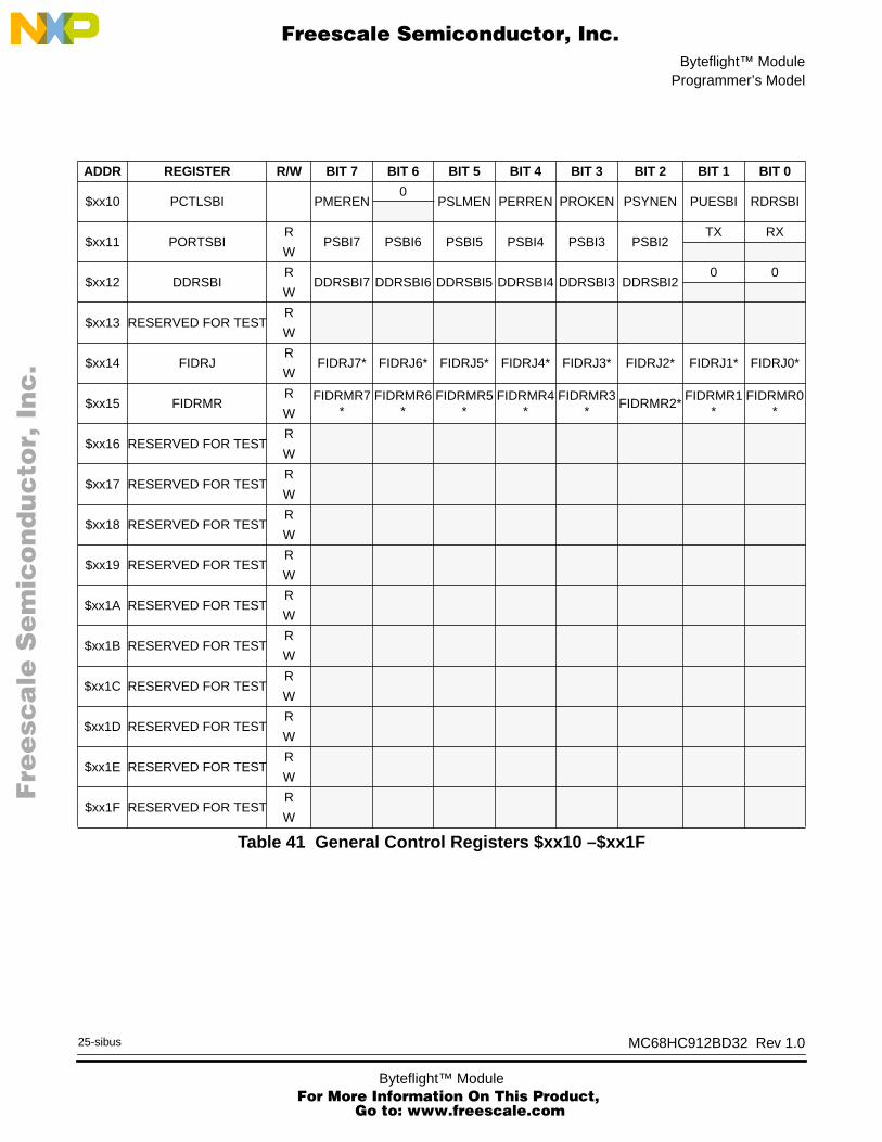
Byteflight™ ModuleProgrammer’s Model
MC68HC912BD32 Rev 1.0
F
ree
sca
le S
em
ico
nd
uc
tor,
I
Freescale Semiconductor, Inc.n
c..
.
25-sibus
ADDR REGISTER R/W BIT 7 BIT 6 BIT 5 BIT 4 BIT 3 BIT 2 BIT 1 BIT 0
$xx10 PCTLSBI PMEREN0
PSLMEN PERREN PROKEN PSYNEN PUESBI RDRSBI
$xx11 PORTSBIR
PSBI7 PSBI6 PSBI5 PSBI4 PSBI3 PSBI2TX RX
W
$xx12 DDRSBIR
DDRSBI7 DDRSBI6 DDRSBI5 DDRSBI4 DDRSBI3 DDRSBI20 0
W
$xx13 RESERVED FOR TESTR
W
$xx14 FIDRJR
FIDRJ7* FIDRJ6* FIDRJ5* FIDRJ4* FIDRJ3* FIDRJ2* FIDRJ1* FIDRJ0*W
$xx15 FIDRMRR FIDRMR7
*FIDRMR6
*FIDRMR5
*FIDRMR4
*FIDRMR3
*FIDRMR2*
FIDRMR1*
FIDRMR0*W
$xx16 RESERVED FOR TESTR
W
$xx17 RESERVED FOR TESTR
W
$xx18 RESERVED FOR TESTR
W
$xx19 RESERVED FOR TESTR
W
$xx1A RESERVED FOR TESTR
W
$xx1B RESERVED FOR TESTR
W
$xx1C RESERVED FOR TESTR
W
$xx1D RESERVED FOR TESTR
W
$xx1E RESERVED FOR TESTR
W
$xx1F RESERVED FOR TESTR
W
Table 41 General Control Registers $xx10 –$xx1F
Byteflight™ Module For More Information On This Product,
Go to: www.freescale.com
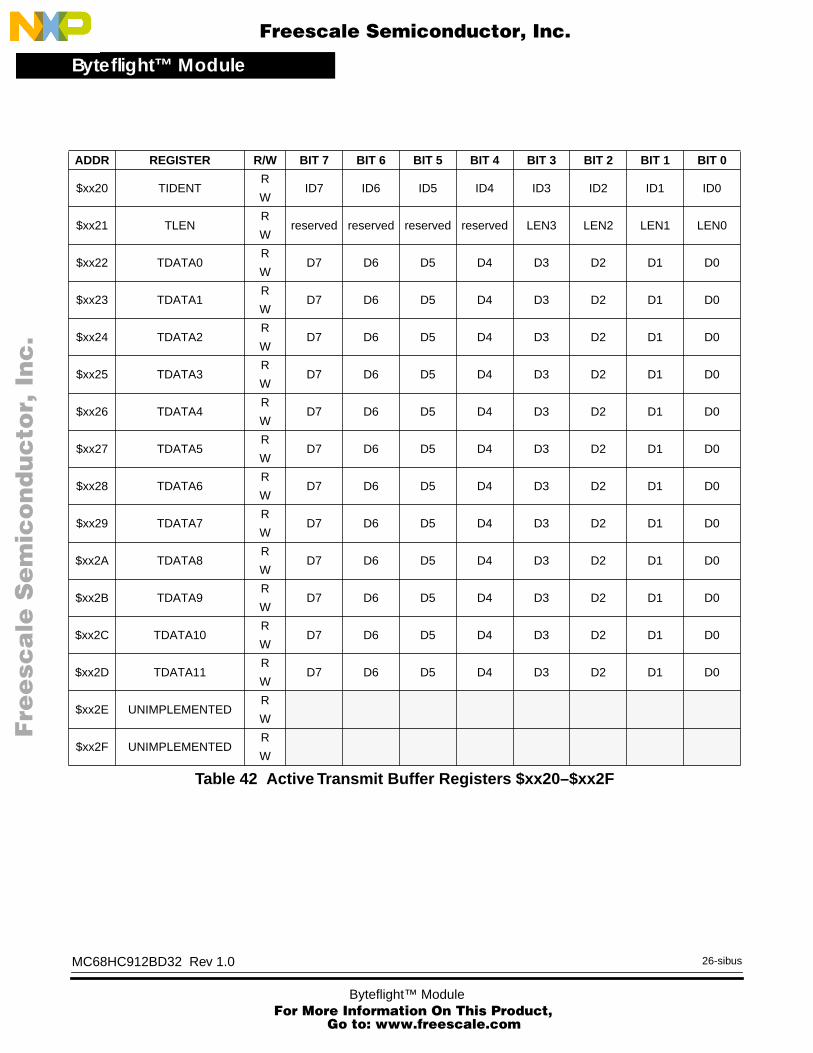
Byteflight™ Module
F
ree
sca
le S
em
ico
nd
uc
tor,
I
Freescale Semiconductor, Inc.n
c..
.
ADDR REGISTER R/W BIT 7 BIT 6 BIT 5 BIT 4 BIT 3 BIT 2 BIT 1 BIT 0
$xx20 TIDENTR
ID7 ID6 ID5 ID4 ID3 ID2 ID1 ID0W
$xx21 TLENR
reserved reserved reserved reserved LEN3 LEN2 LEN1 LEN0W
$xx22 TDATA0R
D7 D6 D5 D4 D3 D2 D1 D0W
$xx23 TDATA1R
D7 D6 D5 D4 D3 D2 D1 D0W
$xx24 TDATA2R
D7 D6 D5 D4 D3 D2 D1 D0W
$xx25 TDATA3R
D7 D6 D5 D4 D3 D2 D1 D0W
$xx26 TDATA4R
D7 D6 D5 D4 D3 D2 D1 D0W
$xx27 TDATA5R
D7 D6 D5 D4 D3 D2 D1 D0W
$xx28 TDATA6R
D7 D6 D5 D4 D3 D2 D1 D0W
$xx29 TDATA7R
D7 D6 D5 D4 D3 D2 D1 D0W
$xx2A TDATA8R
D7 D6 D5 D4 D3 D2 D1 D0W
$xx2B TDATA9R
D7 D6 D5 D4 D3 D2 D1 D0W
$xx2C TDATA10R
D7 D6 D5 D4 D3 D2 D1 D0W
$xx2D TDATA11R
D7 D6 D5 D4 D3 D2 D1 D0W
$xx2E UNIMPLEMENTEDR
W
$xx2F UNIMPLEMENTEDR
W
Table 42 Active Transmit Buffer Registers $xx20–$xx2F
MC68HC912BD32 Rev 1.0
Byteflight™ Module For More Information On This Prod
Go to: www.freescale.com
26-sibus
uct,

Byteflight™ ModuleProgrammer’s Model
MC68HC912BD32 Rev 1.0
F
ree
sca
le S
em
ico
nd
uc
tor,
I
Freescale Semiconductor, Inc.n
c..
.
27-sibus
ADDR REGISTER R/W BIT 7 BIT 6 BIT 5 BIT 4 BIT 3 BIT 2 BIT 1 BIT 0
$xx30 RIDENT*R
ID7 ID6 ID5 ID4 ID3 ID2 ID1 ID0W
$xx31 RLEN*R
reserved reserved reserved reserved LEN3 LEN2 LEN1 LEN0W
$xx32 RDATA0*R
D7 D6 D5 D4 D3 D2 D1 D0W
$xx33 RDATA1*R
D7 D6 D5 D4 D3 D2 D1 D0W
$xx34 RDATA2*R
D7 D6 D5 D4 D3 D2 D1 D0W
$xx35 RDATA3*R
D7 D6 D5 D4 D3 D2 D1 D0W
$xx36 RDATA4*R
D7 D6 D5 D4 D3 D2 D1 D0W
$xx37 RDATA5*R
D7 D6 D5 D4 D3 D2 D1 D0W
$xx38 RDATA6*R
D7 D6 D5 D4 D3 D2 D1 D0W
$xx39 RDATA7*R
D7 D6 D5 D4 D3 D2 D1 D0W
$xx3A RDATA8*R
D7 D6 D5 D4 D3 D2 D1 D0W
$xx3B RDATA9*R
D7 D6 D5 D4 D3 D2 D1 D0W
$xx3C RDATA10*R
D7 D6 D5 D4 D3 D2 D1 D0W
$xx3D RDATA11*R
D7 D6 D5 D4 D3 D2 D1 D0W
$xx3E UNIMPLEMENTEDR
W
$xx3F UNIMPLEMENTEDR
W
Table 43 Active Receive Buffer Registers $xx30–$xx3F
Byteflight™ Module For More Information On This Product,
Go to: www.freescale.com

Byteflight™ Module
F
ree
sca
le S
em
ico
nd
uc
tor,
I
Freescale Semiconductor, Inc.n
c..
.
ADDR REGISTER R/W BIT 7 BIT 6 BIT 5 BIT 4 BIT 3 BIT 2 BIT 1 BIT 0
$xx40 FIDENT*R
ID7 ID6 ID5 ID4 ID3 ID2 ID1 ID0W
$xx41 FLEN*R
reserved reserved reserved reserved LEN3 LEN2 LEN1 LEN0W
$xx42 FDATA0*R
D7 D6 D5 D4 D3 D2 D1 D0W
$xx43 FDATA1*R
D7 D6 D5 D4 D3 D2 D1 D0W
$xx44 FDATA2*R
D7 D6 D5 D4 D3 D2 D1 D0W
$xx45 FDATA3*R
D7 D6 D5 D4 D3 D2 D1 D0W
$xx46 FDATA4*R
D7 D6 D5 D4 D3 D2 D1 D0W
$xx47 FDATA5*R
D7 D6 D5 D4 D3 D2 D1 D0W
$xx48 FDATA6*R
D7 D6 D5 D4 D3 D2 D1 D0W
$xx49 FDATA7*R
D7 D6 D5 D4 D3 D2 D1 D0W
$xx4A FDATA8*R
D7 D6 D5 D4 D3 D2 D1 D0W
$xx4B FDATA9*R
D7 D6 D5 D4 D3 D2 D1 D0W
$xx4C FDATA10*R
D7 D6 D5 D4 D3 D2 D1 D0W
$xx4D FDATA11*R
D7 D6 D5 D4 D3 D2 D1 D0W
$xx4E UNIMPLEMENTEDR
W
$xx4F UNIMPLEMENTEDR
W
Table 44 Active Receive FIFO Buffer Registers $xx40–$xx4F
MC68HC912BD32 Rev 1.0
Byteflight™ Module For More Information On This Prod
Go to: www.freescale.com
28-sibus
uct,

Byteflight™ ModuleProgrammer’s Model
MC68HC912BD32 Rev 1.0
F
ree
sca
le S
em
ico
nd
uc
tor,
I
Freescale Semiconductor, Inc.n
c..
.
29-sibus
ADDR REGISTER R/W BIT 7 BIT 6 BIT 5 BIT 4 BIT 3 BIT 2 BIT 1 BIT 0
$xx50 BUFCTL0R
IFLG IENA LOCKABTAK
ABTRQ0 0
CFG*W
$xx51 BUFCTL1R
IFLG IENA LOCKABTAK
ABTRQ0 0
CFG*W
$xx52 BUFCTL2R
IFLG IENA LOCKABTAK
ABTRQ0 0
CFG*W
$xx53 BUFCTL3R
IFLG IENA LOCKABTAK
ABTRQ0 0
CFG*W
$xx54 BUFCTL4R
IFLG IENA LOCKABTAK
ABTRQ0 0
CFG*W
$xx55 BUFCTL5R
IFLG IENA LOCKABTAK
ABTRQ0 0
CFG*W
$xx56 BUFCTL6R
IFLG IENA LOCKABTAK
ABTRQ0 0
CFG*W
$xx57 BUFCTL7R
IFLG IENA LOCKABTAK
ABTRQ0 0
CFG*W
$xx58 BUFCTL8R
IFLG IENA LOCKABTAK
ABTRQ0 0
CFG*W
$xx59 BUFCTL9R
IFLG IENA LOCKABTAK
ABTRQ0 0
CFG*W
$xx5A BUFCTL10R
IFLG IENA LOCKABTAK
ABTRQ0 0
CFG*W
$xx5B BUFCTL11R
IFLG IENA LOCKABTAK
ABTRQ0 0
CFG*W
$xx5C BUFCTL12R
IFLG IENA LOCKABTAK
ABTRQ0 0
CFG*W
$xx5D BUFCTL13R
IFLG IENA LOCKABTAK
ABTRQ0 0
CFG*W
$xx5E BUFCTL14R
IFLG IENA LOCKABTAK
ABTRQ0 0
CFG*W
$xx5F BUFCTL15R
IFLG IENA LOCKABTAK
ABTRQ0 0
CFG*W
Table 45 Buffer Control Registers $xx50–$xx5F
Byteflight™ Module For More Information On This Product,
Go to: www.freescale.com

Byteflight™ Module
F
ree
sca
le S
em
ico
nd
uc
tor,
I
Freescale Semiconductor, Inc.n
c..
.
Receive and Transmit Message Buffers
There are 16 configurable message buffers, consisting of 14 bytes each. The organization of one message buffer is shown in Figure 34. The first byte contains the 8-bit identifier (ID), the second byte contains the length (LEN) byte (the 4 msb are reserved), followed by a maximum of 12 data bytes (DATA0..11) and two reserved bytes. A LEN value greater than 12 will be transmitted and used in the CRC calculation of transmitter and receiver, but the stored LEN value in the receive buffer will be 12.
The message buffers are configurable as receive, receive FIFO or transmit buffers. The receive and receive FIFO buffer system starts with message buffer 0 and can be configured to the maximum of all 16 message buffers (no transmit buffer). The transmit buffer system starts with message buffer 15 and can be configured to the maximum of all 16 message buffers (no receive buffer).
NOTE: No mixing of receiver, FIFO or transmit buffers is allowed.
Only the ‘active’ buffers (transmit buffer, receive buffer and receive FIFO buffer) are addressable by the CPU and allocate 14 bytes each in the memory map. The ‘non-active’ buffers do not appear in the memory map. To activate a buffer the buffer must be locked. Only one transmit buffer, one receive buffer and one receive FIFO buffer may be locked at a time. A locking error interrupt flag is set and if enabled a locking interrupt is generated when the CPU tries to lock two buffers of the same type.
MC68HC912BD32 Rev 1.0
Byteflight™ Module For More Information On This Prod
Go to: www.freescale.com
30-sibus
uct,

Byteflight™ ModuleProgrammer’s Model
MC68HC912BD32 Rev 1.0
F
ree
sca
le S
em
ico
nd
uc
tor,
I
Freescale Semiconductor, Inc.n
c..
.
31-sibus
Message Buffer Control Registers (BUFCTL15..0)
Each of the 16 configurable message buffers is associated with one Buffer Control Register. All 16 registers are addressable by the CPU. Only a hard reset will clear the register.
CFG — Message Buffer Configuration Bit
This bit is used to configure the corresponding buffer as transmit buffer or as receive or receive FIFO buffer. This bit is readable and is only cleared by hard reset. Writing to this bit is allowed during soft reset only.
1 = The corresponding buffer is configured as transmit buffer.0 = The corresponding buffer is configured as receive buffer or
receive FIFO buffer.
Addr Register Name
$xxx0 Identifier Register
$xxx1 Data Length Register (4 msb reserved)
$xxx2 Data Register 0
$xxx3 Data Register 1
$xxx4 Data Register 2
$xxx5 Data Register 3
$xxx6 Data Register 4
$xxx7 Data Register 5
$xxx8 Data Register 6
$xxx9 Data Register 7
$xxxA Data Register 8
$xxxB Data Register 9
$xxxC Data Register 10
$xxxD Data Register 11
$xxxE reserved
$xxxF reserved
Figure 34 Message Buffer Organization
BIT 7 BIT 6 BIT 5 BIT 4 BIT 3 BIT 2 BIT 1 BIT 0
BUFCTLn RIFLG IENA LOCK
ABTAKABTRQ
0 0CFG*
W
HARDRESET 0 0 0 0 0 0 0 0
Figure 35 Message Buffer Control Registers (BUFCTL15:BUFCTL0)
Byteflight™ Module For More Information On This Product,
Go to: www.freescale.com
Byteflight™ Module
F
ree
sca
le S
em
ico
nd
uc
tor,
I
Freescale Semiconductor, Inc.n
c..
.
ABTRQ — Abort Request
The CPU sets the ABTRQ bit to request that a full transmit buffer (IFLG = 0) is aborted. The request is granted at the next sync pulse if the buffer is still full. The IFLG and the ABTAK flag are set when the message is aborted. The ABTRQ bit is cleared implicitly by setting of the IFLG.
1 = Abort request pending.0 = No abort request.
ABTAK — Abort Acknowledge
This flag acknowledges that a message has been aborted due to a pending abort request from the CPU. The message is aborted at the next sync pulse if the request was pending before the this sync pulse. The application software can use this flag to determine if the message has been sent out or has been aborted. The ABTAK flag is cleared implicitly by clearing the IFLG, i.e. the buffer has been set up again.
1 = The message has been aborted.0 = The message has not been aborted, thus has been sent out.
LOCK — Message Buffer Lock
The bit has various functions depending on the configuration of the corresponding message buffer.
If the buffer is configured as receive buffer and the CPU wants to access the buffer it has to lock it first to prevent an overwrite . The locking is done by writing a “1” to the LOCK bit. Only one receive buffer must be locked at a time. The buffer is released by writing a ‘0’ to the lock bit.
If the buffer is configured as transmit buffer and the CPU wants to access the buffer it has to lock it first. The locking is done by writing a “1” to the LOCK bit. Only one transmit buffer must be locked at a time. The buffer is released by writing a ‘0’ to the lock bit. The request to lock a full tranmit buffer (IFLG = 0) is granted as soon as the buffer has been transmitted.
If there are buffers configured as receive FIFO the LOCK bit of buffer 0 is used for locking the FIFO. Writing a ‘1’ locks the FIFO, no verifying is required. The lock controls the GETIDX. The FIFO buffer addressed by the GETIDX is “visible” in the memory map. The
MC68HC912BD32 Rev 1.0
Byteflight™ Module For More Information On This Prod
Go to: www.freescale.com
32-sibus
uct,

Byteflight™ ModuleProgrammer’s Model
MC68HC912BD32 Rev 1.0
F
ree
sca
le S
em
ico
nd
uc
tor,
I
Freescale Semiconductor, Inc.n
c..
.
33-sibus
GETIDX is incremented when unlocking the FIFO by writing a ‘0’ to the lock bit of buffer 0. Locking a buffer other than buffer 0 within the FIFO does not influence the FIFO window scheme.
NOTE: The lock request is stored, i.e. only one write is necessary. Internal synchronization takes up to two CPU cycle to update the LOCK bit, i.e. the application software should access a locked buffer after verifying the lock bit
IENA — Interrupt Enable Bit
This bit enables the corresponding buffer as interrupt source.1 = The corresponding buffer interrupt enabled.0 = The corresponding buffer interrupt disabled.
IFLG — Interrupt Status Flag
This flag has various functions depending on the configuration of the corresponding message buffer.
If the buffer is configured as receive buffer this flag indicates that the buffer is full. The status flag is cleared if a ‘1’ is written to the bit position. The soft reset value is ‘0’.
1 = Flag set when the receive buffer is full.0 = Flag cleared when the receive buffer is empty.
If the buffer is configured as transmit buffer this flag indicates that the buffer is empty. The status flag is cleared if a ‘1’ is written to the bit position. The soft reset value is ‘1’.
1 = Flag set when the transmit buffer is empty (i.e. has been transmitted or has been aborted).
0 = Flag cleared when the transmit buffer is full and ready for transmit.
If the buffer is configured as receive FIFO buffer this flag has no meaning. It will never be set. The soft reset value is ‘0’.
Byteflight™ Module For More Information On This Product,
Go to: www.freescale.com

Byteflight™ Module
F
ree
sca
le S
em
ico
nd
uc
tor,
I
Freescale Semiconductor, Inc.n
c..
.
Module Configuration Register (MCR)
NOTE: Setting SFTRES and writing to other bits in the MCR can be done in separate instructions only! Trying to set SFTRES and change other bits together will change the SFTRES only, the other bits will be unchanged. Clearing SFTRES and writing to other bits in the MCR can be done in one instruction.
SFTRES — Soft Reset
When this bit is set by the CPU, the module immediately enters the soft reset state. Any ongoing transmission or reception is aborted and synchronization to the bus is lost.
When this bit is cleared by the CPU, the interface will start to connect back to the bus. It will be synchronized after the next SYNC pulse on the bus.
1 = Soft reset state.0 = Normal operation.
MASTER — Master Select
This bit selects the node as bus master or as bus slave. Writing to this bit is allowed during soft reset only.
1 = The interface is a master and generates the SYNC pulses.0 = The interface is a slave and verifies the SYNC pulses.
ALARM — Master Alarm Pulses
If the Master bit and the Alarm bit are set, ALARM pulses are transmitted.
1 = The interface generates ALARM pulses.0 = The interface generates normal SYNC pulses.
The ALARM bit is reset after 255ms - 256ms if it has not been set again by the CPU within that period. The Alarm bit can be set and cleared any time.
BIT 7 BIT 6 BIT 5 BIT 4 BIT 3 BIT 2 BIT 1 BIT 0
MCR RSFTRES MASTER* ALARM
SLPAKSLPRQ WPULSE* SSWAI
0
$xx00 W
HARDRESET 1 0 0 0 0 0 0 0
Figure 36 General Configuration Register (MCR)
MC68HC912BD32 Rev 1.0
Byteflight™ Module For More Information On This Prod
Go to: www.freescale.com
34-sibus
uct,

Byteflight™ ModuleProgrammer’s Model
MC68HC912BD32 Rev 1.0
F
ree
sca
le S
em
ico
nd
uc
tor,
I
Freescale Semiconductor, Inc.n
c..
.
35-sibus
SLPACK — Sleep Acknowledge
This read-only bit indicates that the interface has reached the sleep mode state. This allows an accurate shut off of the module before the shut off of the remaining system.
1 = Module is in sleep mode.0 = Module is in normal run mode.
SLPRQ — Sleep request, enter Low Power Module Sleep Mode
This bit requests the module to enter sleep mode, the clock will be stopped. This allows the module to be shut off when not in use. The CPU can still access the Module Configuration Register. If SLPRQ is asserted in the middle of transmission or reception of a message or is asserted while the temporary message buffers are full, the clock will be stopped at the end of this message, respectively when the temporarily buffers are empty. It remains stopped until a wakeup occurs.
1 = Enter Low Power Sleep Mode.0 = Normal Mode.
WPULSE — Wakeup Pulses
This bit causes to transmit wakeup pulses with the pulse width of t_wake_up. The wakeup sequence is used to wakeup the transceiver from sleep mode. Writing to this bit is allowed during soft reset only.
1 = The interface generates wakeup pulses.0 = The interface does not generate wakeup pulses.
Figure 37 Wakeup Pulses
SSWAI — Serial Bus Interface Stops in Wait Mode1 = The module ceases to be clocked during WAIT mode.0 = The module is not affected during WAIT mode.
t_wake_up
t_wake_up
Byteflight™ Module For More Information On This Product,
Go to: www.freescale.com

Byteflight™ Module
F
ree
sca
le S
em
ico
nd
uc
tor,
I
Freescale Semiconductor, Inc.n
c..
.
FIFO Size Register (FSIZR)
FSIZ4:0 — FIFO Size Bits
These bits are used to configure the FIFO. The number of buffers, starting from buffer ‘0’, assigned to the receive FIFO can be selected. The corresponding buffer(s) must be assigned as Receive buffer by the CFG-bits in the message buffer control register(s).
NOTE: The FSIZR register can only be written if the SFTRES bit in the Module Configuration register is set.
BIT 7 BIT 6 BIT 5 BIT 4 BIT 3 BIT 2 BIT 1 BIT 0
FSIZR R 0 0 0FSIZ4* FSIZ3* FSIZ2* FSIZ1* FSIZ0*
$xx01 W
RESET 0 0 0 0 0 0 0 0
Figure 38 FIFO Size Register (FSIZR)
Table 46 FIFO Size
FSIZ[4:0] FIFO Size
0 0000 No FIFO
0 0001 buffer 0
0 0010 buffers 0, 1
0 0011 buffers 0- 2
: :
01111 buffers 0-14
10000 buffers 0-15
buffers 0-15
11111 buffers 0-15
MC68HC912BD32 Rev 1.0
Byteflight™ Module For More Information On This Prod
Go to: www.freescale.com
36-sibus
uct,

Byteflight™ ModuleProgrammer’s Model
MC68HC912BD32 Rev 1.0
F
ree
sca
le S
em
ico
nd
uc
tor,
I
Freescale Semiconductor, Inc.n
c..
.
37-sibus
Time Configuration Register 1 (TCR1)
The time configuration register 1 contains the specific programmable time t_wx0_tx for the node. Only a hard reset will clear the register.
TWX0T7:TWX0T0 — Time t_wx0_tx
These bits select the Offset Time t_wx0_tx as shown in Table 47.
NOTE: The TCR1 register can only be written if the SFTRES bit in the Module Configuration register is set.
Time Configuration Register 2 (TCR2)
The time configuration register 2 contains the specific programmable time t_wx0_rx for the node. Only a hard reset will clear the register.
TWX0R7:TWX0R0 — Time t_wx0_rx
These bits select the Offset Time t_wx0_rx as shown in Table 48.
NOTE: The TCR2 register can only be written if the SFTRES bit in the Module Configuration register is set.
BIT 7 BIT 6 BIT 5 BIT 4 BIT 3 BIT 2 BIT 1 BIT 0
TCR1 RTWX0T7* TWX0T6* TWX0T5* TWX0T4* TWX0T3* TWX0T2* TWX0T1* TWX0T0*
$xx02 W
HARDRESET 0 0 0 0 0 0 0 0
Figure 39 Time Configuration Register 1 (TCR1)
Table 47 Time t_wx0_tx
TWX0T[7:0] t_wx0_tx[ns]/25 - 7
BIT 7 BIT 6 BIT 5 BIT 4 BIT 3 BIT 2 BIT 1 BIT 0
TCR2 RTWX0R7* TWX0R6* TWX0R5* TWX0R4* TWX0R3* TWX0R2* TWX0R1* TWX0R0*
$xx03 W
HARDRESET 0 0 0 0 0 0 0 0
Figure 40 Time Configuration Register 2 (TCR2)
Table 48 Time t_wx0_rx
TWX0R[7:0] t_wx0_rx[ns]/25 - 7
Byteflight™ Module For More Information On This Product,
Go to: www.freescale.com

Byteflight™ Module
F
ree
sca
le S
em
ico
nd
uc
tor,
I
Freescale Semiconductor, Inc.n
c..
.
TIME CONFIGURATION REGISTER 3 (TCR3)
The time configuration register 3 contains the specific programmable time t_wx_delta for the node. Only a hard reset will clear the register.
TWXD7:TWXD0 — Time t_wx_delta
These bits contain the value for the time t_wx_delta as shown in Table 49.
NOTE: The TCR3 register can only be written if the SFTRES bit in the Module Configuration register is set. The lower bound for TCR3 is 3.
Receive Interrupt Status Register (RISR)
The Receive Interrupt Status Register indicates the occurrence of receive or SYNC pulse events, and together with the Receive Interrupt Enable Register allows the module to operate in a polled or interrupt driven system. Different interrupts can be generated. The Optical Diagnosis Flag (OPTDF) is an indicator for the quality of the optical line between two nodes. The OPTDF flag uses the internal error bit of the optical transceiver which is driven on the Rx line when the photo stream is below a certain level (see ELMOS E100.34 S/E module).
SYNAIF, SYNNIF, SLMMIF, XSYNIF and OPTDF are read and clear only. RCVFIF and RXIF are read only. A flag can be cleared by writing a 1 to the corresponding bit position. Only one write is necessary to request the clearing, i.e. the clear request is stored and executed as soon as the condition which caused the setting is no longer valid. Writing a 0 has no effect on the flag setting. Every flag has an associated interrupt enable flag in the Receive Interrupt Enable Register. A hard or soft reset will clear the register.
BIT 7 BIT 6 BIT 5 BIT 4 BIT 3 BIT 2 BIT 1 BIT 0
TCR3 RTWXD7* TWXD6* TWXD5* TWXD4* TWXD3* TWXD2* TWXD1* TWXD0*
$xx04 W
HARDRESET 0 0 0 0 0 0 0 0
Figure 41 Time Configuration Register 3 (TCR3)
Table 49 Time t_wx_delta calculation
TWXD[7:0] t_wx_delta[ns]/25 - 1
MC68HC912BD32 Rev 1.0
Byteflight™ Module For More Information On This Prod
Go to: www.freescale.com
38-sibus
uct,

Byteflight™ ModuleProgrammer’s Model
MC68HC912BD32 Rev 1.0
F
ree
sca
le S
em
ico
nd
uc
tor,
I
Freescale Semiconductor, Inc.n
c..
.
39-sibus
RCVFIF — Receive FIFO Not Empty Interrupt Flag
This read-only bit will be set when the Receive FIFO is not empty. If enabled, a FIFO not empty interrupt is pending while this flag is set. The flag will be cleared if the FIFO is empty and when buffer 0 is unlocked. The flag remains set if the FIFO is not empty.
1 = Receive FIFO is not empty.0 = Receive FIFO is empty.
NOTE: The RCVFIF flag is cleared two CPU cycles after unlocking buffer 0 if the FIFO is empty, i.e. the application software should not read the RCVFIF flag immediately after unlocking buffer 0.
RXIF — Receive Interrupt Flag
This read-only bit will be set when any of the enabled (IENAn = 1) receive buffers has successfully received a message. It can be cleared by clearing of the IFLG bit(s) of the corresponding buffer(s). If RXIE is set, a receive interrupt is pending while this flag is set.
1 = At least one receive buffer is full.0 = All receive buffers are empty.
NOTE: The RXIF flag is cleared two CPU cycles after clearing of all IFLG bits, i.e. the application software should not read the RXIF flag immediately after clearing the IFLG bit(s).
SYNAIF — Synchronization Pulse ALARM Interrupt Flag
This bit will be set when a SYNC pulse ALARM has been received. If enabled, a SYNC pulse interrupt is pending while this flag is set.
1 = SYNC pulse ALARM has been received.0 = No SYNC pulse ALARM has occurred.
SYNNIF — Synchronization Pulse NORMAL Interrupt Flag
This bit will be set when a SYNC pulse NORMAL has been received. If enabled, a SYNC pulse interrupt is pending while this flag is set.
BIT 7 BIT 6 BIT 5 BIT 4 BIT 3 BIT 2 BIT 1 BIT 0
RISR R RCVFIF RXIFSYNAIF SYNNIF SLMMIF
0XSYNIF OPTDF
$xx06 W
H/S-RESET 0 0 0 0 0 0 0 0
Figure 42 Receive Interrupt Status Register (RISR)
Byteflight™ Module For More Information On This Product,
Go to: www.freescale.com

Byteflight™ Module
F
ree
sca
le S
em
ico
nd
uc
tor,
I
Freescale Semiconductor, Inc.n
c..
.
1 = SYNC pulse NORMAL has been received.0 = No SYNC pulse NORMAL has occurred.
SLMMIF — Slot Mismatch Interrupt Flag
This bit will be set when the identifier of a successfully received message differs from the current time slot.
1 = A mismatch between successfully received identifier and slot counter has occurred.
0 = No slot mismatch has occurred.
XSYNIF — XSYNC Pulse Interrupt Flag
This bit will be set when a valid SYNC pulse (NORMAL or ALARM Sync pulse) has been received. If enabled, an XSYNC pulse interrupt is pending while the flag is set.
1 = SYNC pulse has been received.0 = No SYNC pulse has occurred.
OPTDF — Optical Diagnosis Flag
This bit will be set when the internal error bit of the optical transceiver is driven on the Rx line during transmission.
1 = A pulse on Rx has been detected.0 = No pulse on Rx has been detected.
General Interrupt Status Register (GISR)
The General Interrupt Status Register indicates the occurrence of system events, and together with the General Interrupt Enable Register allows the module to operate in a polled or interrupt driven system. A general interrupt can be generated.
OVRNIF, ERRIF, SYNEIF, SYNLIF, ILLPIF and WAKEIF are read and clear only. TXIF and LOCKIF are read only. A flag can be cleared by writing a 1 to the corresponding bit position. Only one write is necessary to request the clearing, i.e. the clear request is stored and excuted as soon as the condition which caused the setting is no longer valid. SYNLIF can only cleared after receiving a valid sync pulse. Writing a 0 has no effect on the flag setting. Every flag has an associated interrupt enable bit in the General Interrupt Enable Register. A hard or soft reset will clear the register (except LOCKIF, which can only be cleared by a hard or system reset).
MC68HC912BD32 Rev 1.0
Byteflight™ Module For More Information On This Prod
Go to: www.freescale.com
40-sibus
uct,
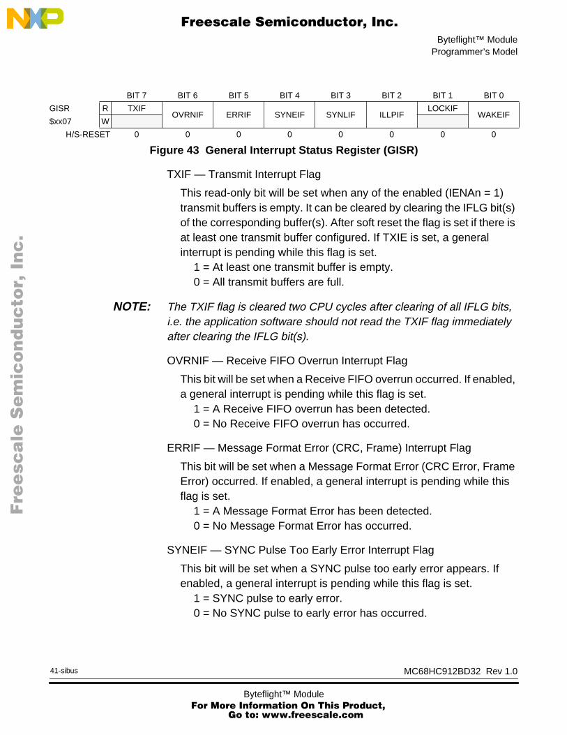
Byteflight™ ModuleProgrammer’s Model
MC68HC912BD32 Rev 1.0
F
ree
sca
le S
em
ico
nd
uc
tor,
I
Freescale Semiconductor, Inc.n
c..
.
41-sibus
TXIF — Transmit Interrupt Flag
This read-only bit will be set when any of the enabled (IENAn = 1) transmit buffers is empty. It can be cleared by clearing the IFLG bit(s) of the corresponding buffer(s). After soft reset the flag is set if there is at least one transmit buffer configured. If TXIE is set, a general interrupt is pending while this flag is set.
1 = At least one transmit buffer is empty.0 = All transmit buffers are full.
NOTE: The TXIF flag is cleared two CPU cycles after clearing of all IFLG bits, i.e. the application software should not read the TXIF flag immediately after clearing the IFLG bit(s).
OVRNIF — Receive FIFO Overrun Interrupt Flag
This bit will be set when a Receive FIFO overrun occurred. If enabled, a general interrupt is pending while this flag is set.
1 = A Receive FIFO overrun has been detected.0 = No Receive FIFO overrun has occurred.
ERRIF — Message Format Error (CRC, Frame) Interrupt Flag
This bit will be set when a Message Format Error (CRC Error, Frame Error) occurred. If enabled, a general interrupt is pending while this flag is set.
1 = A Message Format Error has been detected.0 = No Message Format Error has occurred.
SYNEIF — SYNC Pulse Too Early Error Interrupt Flag
This bit will be set when a SYNC pulse too early error appears. If enabled, a general interrupt is pending while this flag is set.
1 = SYNC pulse to early error.0 = No SYNC pulse to early error has occurred.
BIT 7 BIT 6 BIT 5 BIT 4 BIT 3 BIT 2 BIT 1 BIT 0
GISR R TXIFOVRNIF ERRIF SYNEIF SYNLIF ILLPIF
LOCKIFWAKEIF
$xx07 W
H/S-RESET 0 0 0 0 0 0 0 0
Figure 43 General Interrupt Status Register (GISR)
Byteflight™ Module For More Information On This Product,
Go to: www.freescale.com

Byteflight™ Module
F
ree
sca
le S
em
ico
nd
uc
tor,
I
Freescale Semiconductor, Inc.n
c..
.
SYNLIF — SYNC Pulse Lost Error Interrupt Flag
This bit will be set when a SYNC pulse lost error appears. If enabled, a general interrupt is pending while this flag is set. The flag is enabled as soon as the first valid normal/alarm synchronization pulse has been detected.
1 = SYNC pulse lost error.0 = No SYNC pulse lost error has occurred.
ILLPIF — Illegal Pulse Error Interrupt Flag
This bit will be set when an illegal pulse error appears. If enabled, a general interrupt is pending while this flag is set.
1 = Illegal pulse error.0 = No illegal pulse error has occurred.
LOCKIF — Locking Error Interrupt Flag
This bit will be set when two Rx buffers or two Tx buffers are locked at the same time. If enabled, a general interrupt is pending while this flag is set and the module enters soft reset. The bit is only cleared by a hard or system reset.
1 = Locking error.0 = No locking error has occurred.
WAKEIF — WAKEUP Interrupt Flag
This bit will be set when the module detects bus activity whilst it is asleep. If enabled, a general interrupt is pending while this flag is set.
1 = Detected activity on the bus.0 = No wake-up activity has been observed while in sleep mode.
MC68HC912BD32 Rev 1.0
Byteflight™ Module For More Information On This Prod
Go to: www.freescale.com
42-sibus
uct,

Byteflight™ ModuleProgrammer’s Model
MC68HC912BD32 Rev 1.0
F
ree
sca
le S
em
ico
nd
uc
tor,
I
Freescale Semiconductor, Inc.n
c..
.
43-sibus
Receive Interrupt Enable Register (RIER)
The Receive Interrupt Enable Register allows to enable/disable the different receive or SYNC pulse interrupt sources for different interrupt requests. A hard or soft reset will clear the register.
RCVFIE — Receive FIFO Not Empty Interrupt Enable1 = A Receive FIFO not empty event will result in a receive FIFO
not empty interrupt.0 = No interrupt will be generated from this event.
RXIE — Receive Interrupt Enable1 = A receive event will result in a receive interrupt.0 = No interrupt will be generated from this event.
SYNAIE — Synchronization Pulse ALARM Interrupt Enable1 = A SYNC pulse ALARM event will result in a SYNC pulse
interrupt.0 = No interrupt will be generated from this event.
SYNNIE — Synchronization Pulse NORMAL Interrupt Enable1 = A SYNC pulse NORMAL event will result in a SYNC pulse
interrupt.0 = No interrupt will be generated from this event.
SLMMIE — Slot Mismatch Interrupt Enable1 = A slot mismatch event will result in a general interrupt.0 = No interrupt will be generated from this event.
XSYNIE — Xsync Pulse Interrupt Enable1 = A SYNC pulse event will result in an XSYNC pulse interrupt.0 = No interrupt will be generated from this event.
BIT 7 BIT 6 BIT 5 BIT 4 BIT 3 BIT 2 BIT 1 BIT 0
RIER RRCVFIE RXIE SYNAIE SYNNIE SLMMIE
0XSYNIE
0
$xx08 W
H/S-RESET 0 0 0 0 0 0 0 0
Figure 44 Receive Interrupt Enable Register (RIER)
Byteflight™ Module For More Information On This Product,
Go to: www.freescale.com

Byteflight™ Module
F
ree
sca
le S
em
ico
nd
uc
tor,
I
Freescale Semiconductor, Inc.n
c..
.
General Interrupt Enable Register (GIER)
The General Interrupt Enable Register allows to enable/disable the different interrupt sources for the general interrupt request. A hard or soft reset will clear the register.
TXIE — Transmit Interrupt Enable1 = A transmit event will result in a general interrupt.0 = No interrupt will be generated from this event.
OVRNIE — Receive FIFO Overrun Interrupt Enable1 = A Receive FIFO overrun event will result in a general interrupt.0 = No interrupt will be generated from this event.
ERRIE — Message Format Error (CRC or Frame) Interrupt Enable1 = A Message Format Error will result in a general interrupt.0 = No interrupt will be generated from this event.
SYNEIE — SYNC Pulse Too Early Error Interrupt Enable1 = A SYNC pulse too early error will result in a general interrupt.0 = No interrupt will be generated from this event.
SYNLIE — SYNC Pulse Lost Error Interrupt Enable1 = A SYNC pulse lost error will result in a general interrupt.0 = No interrupt will be generated from this event.
ILLPIE — Illegal Pulse Error Interrupt Enable1 = An illegal pulse error will result in a general interrupt.0 = No interrupt will be generated from this event.
BIT 7 BIT 6 BIT 5 BIT 4 BIT 3 BIT 2 BIT 1 BIT 0
GIER RTXIE OVRNIE ERRIE SYNEIE SYNLIE ILLPIE LOCKIE* WAKEIE
$xx09 W
H/S-RESET 0 0 0 0 0 0 0 0
Figure 45 General Interrupt Enable Register (GIER)
MC68HC912BD32 Rev 1.0
Byteflight™ Module For More Information On This Prod
Go to: www.freescale.com
44-sibus
uct,
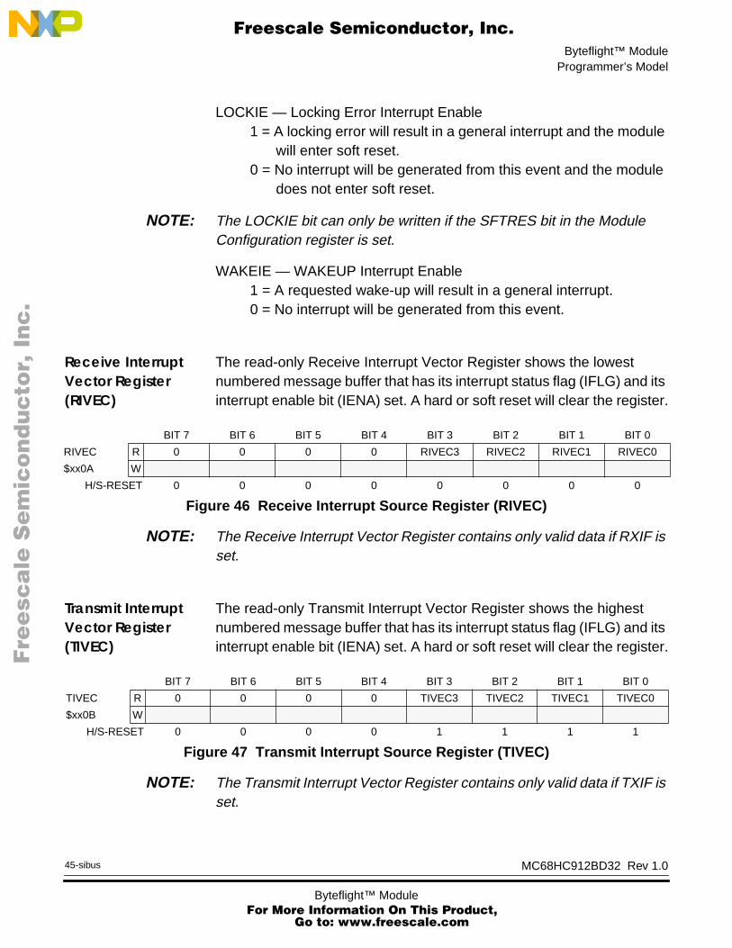
Byteflight™ ModuleProgrammer’s Model
MC68HC912BD32 Rev 1.0
F
ree
sca
le S
em
ico
nd
uc
tor,
I
Freescale Semiconductor, Inc.n
c..
.
45-sibus
LOCKIE — Locking Error Interrupt Enable1 = A locking error will result in a general interrupt and the module
will enter soft reset.0 = No interrupt will be generated from this event and the module
does not enter soft reset.
NOTE: The LOCKIE bit can only be written if the SFTRES bit in the Module Configuration register is set.
WAKEIE — WAKEUP Interrupt Enable1 = A requested wake-up will result in a general interrupt.0 = No interrupt will be generated from this event.
Receive Interrupt Vector Register (RIVEC)
The read-only Receive Interrupt Vector Register shows the lowest numbered message buffer that has its interrupt status flag (IFLG) and its interrupt enable bit (IENA) set. A hard or soft reset will clear the register.
NOTE: The Receive Interrupt Vector Register contains only valid data if RXIF is set.
Transmit Interrupt Vector Register (TIVEC)
The read-only Transmit Interrupt Vector Register shows the highest numbered message buffer that has its interrupt status flag (IFLG) and its interrupt enable bit (IENA) set. A hard or soft reset will clear the register.
NOTE: The Transmit Interrupt Vector Register contains only valid data if TXIF is set.
BIT 7 BIT 6 BIT 5 BIT 4 BIT 3 BIT 2 BIT 1 BIT 0
RIVEC R 0 0 0 0 RIVEC3 RIVEC2 RIVEC1 RIVEC0
$xx0A W
H/S-RESET 0 0 0 0 0 0 0 0
Figure 46 Receive Interrupt Source Register (RIVEC)
BIT 7 BIT 6 BIT 5 BIT 4 BIT 3 BIT 2 BIT 1 BIT 0
TIVEC R 0 0 0 0 TIVEC3 TIVEC2 TIVEC1 TIVEC0
$xx0B W
H/S-RESET 0 0 0 0 1 1 1 1
Figure 47 Transmit Interrupt Source Register (TIVEC)
Byteflight™ Module For More Information On This Product,
Go to: www.freescale.com
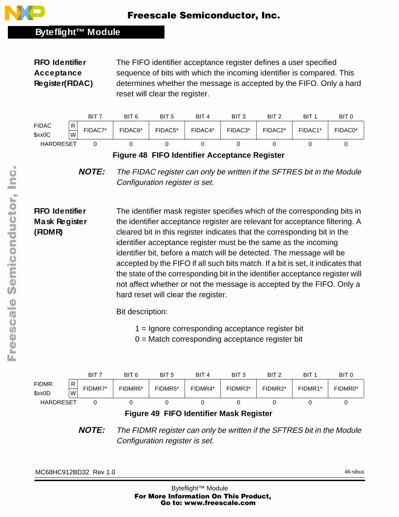
Byteflight™ Module
F
ree
sca
le S
em
ico
nd
uc
tor,
I
Freescale Semiconductor, Inc.n
c..
.
FIFO Identifier Acceptance Register(FIDAC)
The FIFO identifier acceptance register defines a user specified sequence of bits with which the incoming identifier is compared. This determines whether the message is accepted by the FIFO. Only a hard reset will clear the register.
NOTE: The FIDAC register can only be written if the SFTRES bit in the Module Configuration register is set.
FIFO Identifier Mask Register (FIDMR)
The identifier mask register specifies which of the corresponding bits in the identifier acceptance register are relevant for acceptance filtering. A cleared bit in this register indicates that the corresponding bit in the identifier acceptance register must be the same as the incoming identifier bit, before a match will be detected. The message will be accepted by the FIFO if all such bits match. If a bit is set, it indicates that the state of the corresponding bit in the identifier acceptance register will not affect whether or not the message is accepted by the FIFO. Only a hard reset will clear the register.
Bit description:
1 = Ignore corresponding acceptance register bit0 = Match corresponding acceptance register bit
NOTE: The FIDMR register can only be written if the SFTRES bit in the Module Configuration register is set.
BIT 7 BIT 6 BIT 5 BIT 4 BIT 3 BIT 2 BIT 1 BIT 0
FIDAC RFIDAC7* FIDAC6* FIDAC5* FIDAC4* FIDAC3* FIDAC2* FIDAC1* FIDAC0*
$xx0C W
HARDRESET 0 0 0 0 0 0 0 0
Figure 48 FIFO Identifier Acceptance Register
BIT 7 BIT 6 BIT 5 BIT 4 BIT 3 BIT 2 BIT 1 BIT 0
FIDMR RFIDMR7* FIDMR6* FIDMR5* FIDMR4* FIDMR3* FIDMR2* FIDMR1* FIDMR0*
$xx0D W
HARDRESET 0 0 0 0 0 0 0 0
Figure 49 FIFO Identifier Mask Register
MC68HC912BD32 Rev 1.0
Byteflight™ Module For More Information On This Prod
Go to: www.freescale.com
46-sibus
uct,

Byteflight™ ModuleProgrammer’s Model
MC68HC912BD32 Rev 1.0
F
ree
sca
le S
em
ico
nd
uc
tor,
I
Freescale Semiconductor, Inc.n
c..
.
47-sibus
FIFO Identifier Rejection Register (FIDRJ)
The FIFO identifier rejection register defines a user specified sequence of bits with which the incoming identifier is compared. This determines whether the message is rejected by the FIFO. Only a hard reset will clear the register.
NOTE: The FIDRJ register can only be written if the SFTRES bit in the Module Configuration register is set.
FIFO Identifier Rejection Mask Register (FIDRMR)
The identifier rejection mask register specifies which of the corresponding bits in the identifier rejection register are relevant for rejection filtering. A cleared bit in this register indicates that the corresponding bit in the identifier rejection register must be the same as the incoming identifier bit, before a match will be detected. The message will be rejected by the FIFO if all such bits match. If a bit is set, it indicates that the state of the corresponding bit in the identifier rejection register will not affect whether or not the message is rejected by the FIFO. Only a hard reset will set the register.
Bit description:1 = Ignore corresponding rejection register bit0 = Match corresponding rejection register bit
NOTE: The FIDRMR register can only be written if the SFTRES bit in the Module Configuration register is set.
BIT 7 BIT 6 BIT 5 BIT 4 BIT 3 BIT 2 BIT 1 BIT 0
FIDRJ RFIDRJ7* FIDRJ6* FIDRJ5* FIDRJ4* FIDRJ3* FIDRJ2* FIDRJ1* FIDRJ0*
$xx14 W
HARDRESET 0 0 0 0 0 0 0 0
Figure 50 FIFO Identifier Rejection Register
BIT 7 BIT 6 BIT 5 BIT 4 BIT 3 BIT 2 BIT 1 BIT 0
FIDRMR RFIDRMR7* FIDRMR6* FIDRMR5* FIDRMR4* FIDRMR3* FIDRMR2* FIDRMR1* FIDRMR0*
$xx15 W
HARDRESET 1 1 1 1 1 1 1 1
Table 50 FIFO Rejection Mask Register
Byteflight™ Module For More Information On This Product,
Go to: www.freescale.com

Byteflight™ Module
F
ree
sca
le S
em
ico
nd
uc
tor,
I
Freescale Semiconductor, Inc.n
c..
.
Module Version Register (MVR)
The read-only Module Version Register contains the version number of the implementation.
Byteflight™ Port SBI Control Register (PCTLSBI)
The following bits control pins of Port SBI. Pins 1 and 0 are reserved for the Rx (input only) and Tx (output only) pins. Only a hard reset will clear the register.
PMEREN — Slot Mismatch Error Enable1 = A 50ns pulse is driven on Port SBI4 after a slot mismatch.0 = Port SBI4 is a general IO pin.
PSLMEN — Slot Mismatch Enable1 = A 50ns pulse is driven on Port SBI5 after a slot mismatch.0 = Port SBI5 is a general IO pin.
PERREN — Error Pulse Enable1 = A 50ns pulse is driven on Port SBI4 after a message format or
illegal pulse error.0 = Port SBI4 is a general IO pin.
PROKEN — Reception OK Pulse Enable1 = A 50ns pulse is driven on Port SBI3 after the successful
reception of a message or sync pulse.0 = Port SBI3 is a general IO pin.
BIT 7 BIT 6 BIT 5 BIT 4 BIT 3 BIT 2 BIT 1 BIT 0
MVR R MVR7 MVR6 MVR5 MVR4 MVR3 MVR2 MVR1 MVR0
$xx0E W
Figure 51 Module Version Register (MVR)
BIT 7 BIT 6 BIT 5 BIT 4 BIT 3 BIT 2 BIT 1 BIT 0
PCTLSBI RPMEREN
0PSLMEN PERREN PROKEN PSYNEN PUESBI RDRSBI
$xx10 W
HARDRESET 0 0 0 0 0 0 0 0
Figure 52 Port SBI Control Register (PCTLSBI)
MC68HC912BD32 Rev 1.0
Byteflight™ Module For More Information On This Prod
Go to: www.freescale.com
48-sibus
uct,

Byteflight™ ModuleProgrammer’s Model
MC68HC912BD32 Rev 1.0
F
ree
sca
le S
em
ico
nd
uc
tor,
I
Freescale Semiconductor, Inc.n
c..
.
49-sibus
PSYNEN — Sync Pulse Enable1 = A 50ns pulse is driven on Port SBI2 after the successful
reception or transmission of a sync pulse.0 = Port SBI2 is a general IO pin.
PUESBI — Pull Up Enable Port SBI1 = Pull up enabled for Port SBI.0 = Pull up disabled for Port SBI.
RDRSBI — Reduced Drive Port SBI1 = Reduced drive enabled for Port SBI.0 = Reduced drive disabled for Port SBI.
Byteflight™ Port SBI Data Register (PORTSBI
PSBI7 – PSBI2 — Port SBI Data Bits
Writing to PSBIx stores the bit value in an internal bit memory. This value is driven to the respective pin only if DDRSBIx = 1. Only a hard reset will clear the register.
Reading PSBIx returns
• the value of the internal bit memory driven to the pin, if DDRSBIx = 1
• the value of the respective pin, if DDRSBIx = 0
Reading bits 1 and 0 returns the value of the Tx and Rx pins, respectively.
BIT 7 BIT 6 BIT 5 BIT 4 BIT 3 BIT 2 BIT 1 BIT 0
PORTSBI RPSBI7 PSBI6 PSBI5 PSBI4 PSBI3 PSBI2
TX RX
$xx11 W
HARDRESET U U U U U U U U
Figure 53 Port SBI Data Register (PORTSBI)
Byteflight™ Module For More Information On This Product,
Go to: www.freescale.com

Byteflight™ Module
F
ree
sca
le S
em
ico
nd
uc
tor,
I
Freescale Semiconductor, Inc.n
c..
.
Byteflight™ Port SBI Data Direction Register (DDRSBI)
DDRSBI7 – DDRSBI2 — Data Direction Port SBI Bits1 = Respective I/O pin is configured for output.0 = Respective I/O pin is configured for input.
The Port SBI5–2 pins are outputs, if PMEREN, PSLMEN, PERREN, PROKEN and PSYNEN are set, regardless of their corresponding Data Direction Bits. Only a hard reset will clear the register.
Initialization
To ensure correct operation, use the following initialization procedure:
• Enter the soft reset mode by setting the SFTRES bit (MCR)
• Desired setting of module configuration register (MCR) – Master or Slave select, MASTER bit
• Desired setting of the FIFO Size register (FSIZR) – configure FIFO size, FSIZ4:0 bits
• Desired setting of time configuration registers (TCR1–TCR3)
• Desired setting of the message buffer control registers (BUFCTL15..0) – configure the buffers as transmit or receive buffers
– enable/disable of the corresponding interrupt, IENA bits
• Set FIFO acceptance register (FIDAC) and mask register (FIDMR).
• Exit the soft reset mode by resetting the SFTRES bit (MCR)
BIT 7 BIT 6 BIT 5 BIT 4 BIT 3 BIT 2 BIT 1 BIT 0
DDRSBI RDDRSBI7 DDRSBI6 DDRSBI5 DDRSBI4 DDRSBI3 DDRSBI2
0 0
$xx12 W
HARDRESET 0 0 0 0 0 0 0 0
Figure 54 Port SBI Data Direction Register (DDRSBI)
MC68HC912BD32 Rev 1.0
Byteflight™ Module For More Information On This Prod
Go to: www.freescale.com
50-sibus
uct,

Byteflight™ ModuleFIFO Usage
MC68HC912BD32 Rev 1.0
F
ree
sca
le S
em
ico
nd
uc
tor,
I
Freescale Semiconductor, Inc.n
c..
.
51-sibus
FIFO Usage
The user’s receive FIFO handler has to run the following procedure assuming the FIFO is not empty:
• lock the FIFO buffer by setting the LOCK bit of buffer 0, the buffer with the oldest unaccessed message, addressed by GETIDX, appears in the memory map
• copy over the message
• unlock the FIFO buffer, the GETIDX will be incremented
Unlocking an empty FIFO does not increment the GETIDX and does not set the FIFO empty flag.
Byteflight™ Module For More Information On This Product,
Go to: www.freescale.com

Byteflight™ Module
F
ree
sca
le S
em
ico
nd
uc
tor,
I
Freescale Semiconductor, Inc.n
c..
.
MC68HC912BD32 Rev 1.0
Byteflight™ Module For More Information On This Prod
Go to: www.freescale.com
52-sibus
uct,

F
ree
sca
le S
em
ico
nd
uc
tor,
IFreescale Semiconductor, Inc.
nc
...
Analog to Digital ConverterAnalog to Digital Converter
Contents
Introduction . . . . . . . . . . . . . . . . . . . . . . . . . . . . . . . . . . . . . . . . . . . . 219Functional Description. . . . . . . . . . . . . . . . . . . . . . . . . . . . . . . . . . . . 220ATD Registers. . . . . . . . . . . . . . . . . . . . . . . . . . . . . . . . . . . . . . . . . . 221ATD Mode Operation . . . . . . . . . . . . . . . . . . . . . . . . . . . . . . . . . . . . 230
Introduction
The ATD is an 8-channel, 10-bit, multiplexed-input successive-approximation analog-to-digital converter, accurate to ±2 least significant bits (LSB). It does not require external sample and hold circuits because of the type of charge redistribution technique used. The ATD converter timing is synchronized to the system P clock. The ATD module consists of a 16-word (32-byte) memory-mapped control register block used for control, testing and configuration.
MC68HC912BD32 Rev 1.0
1-adcAnalog to Digital Converter For More Information On This Product,
Go to: www.freescale.com

Analog to Digital Converter
F
ree
sca
le S
em
ico
nd
uc
tor,
I
Freescale Semiconductor, Inc.n
c..
.
Figure 55 Analog-to-Digital Converter Block Diagram
Functional Description
A single conversion sequence consists of four or eight conversions, depending on the state of the select 8 channel mode (S8CM) bit when ATDCTL5 is written. There are eight basic conversion modes. In the non-scan modes, the SCF bit is set after the sequence of four or eight conversions has been performed and the ATD module halts. In the scan modes, the SCF bit is set after the first sequence of four or eight conversions has been performed, and the ATD module continues to restart the sequence. In both modes, the CCF bit associated with each register is set when that register is loaded with the appropriate conversion result. That flag is cleared automatically when that result register is read. The conversions are started by writing to the control registers.
MO
DE
AND
TIM
ING
CO
NTR
OLS
ATD 0
ATD 1
ATD 2
ATD 3
ATD 4
ATD 5
ATD 6
ATD 7
SAR
RC DAC ARRAYAND COMPARATOR
INTERNAL BUS
VDDA
VSSA
VRL
VRH
CLOCKSELECT/PRESCALE
ANALOG MUXAND
SAMPLE BUFFER AMP
PORT ADDATA INPUT REGISTER
AN7/PAD7AN6/PAD6AN5/PAD5AN4/PAD4AN3/PAD3AN2/PAD2AN1/PAD1AN0/PAD0
REFERENCE
SUPPLY
MC68HC912BD32 Rev 1.0
Analog to Digital Converter For More Information On This Prod
Go to: www.freescale.com
2-adc
uct,

Analog to Digital ConverterATD Registers
F
ree
sca
le S
em
ico
nd
uc
tor,
I
Freescale Semiconductor, Inc.n
c..
.
ATD Registers
Write to this register will abort current conversion sequence. READ: any time, WRITE: any time.
WRITE: write to this register has no meaning. READ: Special Mode only.
The ATD control register 2 and 3 are used to select the power up mode, interrupt control, and freeze control. Writes to these registers abort any current conversion sequence.
Read or write anytime except ASCIF bit, which cannot be written.
Bit positions ATDCTL2[4:2] and ATDCTL3[7:2] are unused and always read as zeros.
ADPU — ATD Disable0 = Disables the ATD, including the analog section for reduction in
power consumption.1 = Allows the ATD to function normally.
Software can disable the clock signal to the ATD converter and power down the analog circuits to reduce power consumption. When reset to zero, the ADPU bit aborts any conversion sequence in progress.
ATDCTL0 — Reserved $0060
Bit 7 6 5 4 3 2 1 Bit 0
0 0 0 0 0 0 0 0
RESET: 0 0 0 0 0 0 0 0
ATDCTL1 — Reserved $0061
Bit 7 6 5 4 3 2 1 Bit 0
0 0 0 0 0 0 0 0
RESET: 0 0 0 0 0 0 0 0
ATDCTL2 — ATD Control Register 2 $0062
Bit 7 6 5 4 3 2 1 Bit 0
ADPU AFFC AWAI 0 0 0 ASCIE ASCIF
RESET: 0 0 0 0 0 0 0 0
MC68HC912BD32 Rev 1.0
3-adcAnalog to Digital Converter For More Information On This Product,
Go to: www.freescale.com

Analog to Digital Converter
F
ree
sca
le S
em
ico
nd
uc
tor,
I
Freescale Semiconductor, Inc.n
c..
.
Because the bias currents to the analog circuits are turned off, the ATD requires a period of recovery time to stabilize the analog circuits after setting the ADPU bit.
AFFC — ATD Fast Flag Clear All0 = ATD flag clearing operates normally (read the status register
before reading the result register to clear the associate CCF bit).
1 = Changes all ATD conversion complete flags to a fast clear sequence. Any access to a result register (ATD0–7) will cause the associated CCF flag to clear automatically if it was set at the time.
AWAI — ATD Stop in Wait Mode0 = ATD continues to run when the MCU is in wait mode1 = ATD stops to save power when the MCU is in wait mode
ASCIE — ATD Sequence Complete Interrupt Enable0 = Disables ATD interrupt1 = Enables ATD interrupt on sequence complete
ASCIF — ATD Sequence Complete Interrupt
Cannot be written in any mode.0 = No ATD interrupt occurred1 = ATD sequence complete
FRZ1, FRZ0 — Background Debug (Freeze) Enable (suspend module operation at breakpoint)
When debugging an application, it is useful in many cases to have the ATD pause when a breakpoint is encountered. These two bits determine how the ATD will respond when background debug mode becomes active.
ATDCTL3 — ATD Control Register 3 $0063
Bit 7 6 5 4 3 2 1 Bit 0
0 0 0 0 0 0 FRZ1 FRZ0
RESET: 0 0 0 0 0 0 0 0
MC68HC912BD32 Rev 1.0
Analog to Digital Converter For More Information On This Prod
Go to: www.freescale.com
4-adc
uct,

Analog to Digital ConverterATD Registers
F
ree
sca
le S
em
ico
nd
uc
tor,
I
Freescale Semiconductor, Inc.n
c..
.
The ATD control register 4 is used to select the clock source and set up the prescaler. Writes to the ATD control registers initiate a new conversion sequence. If a write occurs while a conversion is in progress, the conversion is aborted and ATD activity halts until a write to ATDCTL5 occurs.
S10BM — ATD 10-bit Mode Control0 = 8 bit operation1 = 10 bit operation
SMP1, SMP0 — Select Sample Time
These bits are used to select one of four sample times after the buffered sample and transfer has occurred.
PRS4, PRS3, PRS2, PRS1, PRS0 — Select Divide-By Factor for ATD P-Clock Prescaler.
The binary value written to these bits (1 to 31) selects the divide-by factor for the modulo counter-based prescaler. The P clock is divided by this value plus one and then fed into a ÷2 circuit to generate the
Table 51 ATD Response to Background Debug Enable
FRZ1 FRZ0 ATD Response
0 0 Continue conversions in active background mode
0 1 Reserved
1 0 Finish current conversion, then freeze
1 1 Freeze when BDM is active
ATDCTL4 — ATD Control Register 4 $0064
Bit 7 6 5 4 3 2 1 Bit 0
S10BM SMP1 SMP0 PRS4 PRS3 PRS2 PRS1 PRS0
RESET: 0 0 0 0 0 0 0 1
Table 52 Final Sample Time Selection
SMP1 SMP0 Final Sample Time Total 8-Bit Conversion Time Total 10-Bit Conversion Time
0 0 2 ATD clock periods 18 ATD clock periods 20 ATD clock periods
0 1 4 ATD clock periods 20 ATD clock periods 22 ATD clock periods
1 0 8 ATD clock periods 24 ATD clock periods 26 ATD clock periods
1 1 16 ATD clock periods 32 ATD clock periods 34 ATD clock periods
MC68HC912BD32 Rev 1.0
5-adcAnalog to Digital Converter For More Information On This Product,
Go to: www.freescale.com

Analog to Digital Converter
F
ree
sca
le S
em
ico
nd
uc
tor,
I
Freescale Semiconductor, Inc.n
c..
.
ATD module clock. The divide-by-two circuit insures symmetry of the output clock signal. Clearing these bits causes the prescale value default to one which results in a ÷2 prescale factor. This signal is then fed into the ÷2 logic. The reset state divides the P clock by a total of four and is appropriate for nominal operation between 2 MHz and 8 MHz bus rate. For operation at 10 MHz this value must be reprogrammed first to ÷6 or greater before using the ATD. Table 53 shows the divide-by operation and the appropriate range of system clock frequencies.
The ATD control register 5 is used to select the conversion modes, the conversion channel(s), and initiate conversions.
Read or write anytime. A write to ATDCTL5 initiates a new conversion sequence. If a conversion sequence is in progress when a write occurs, that sequence is aborted and the SCF and CCF bits are reset.
S8CM — Select 8 Channel Mode
Table 53 Clock Prescaler Values
Prescale Value Total Divisor Max P Clock (1)
1. Maximum conversion frequency is 2 MHz. Maximum P clock divisor value will becomemaximum conversion rate that can be used on this ATD module.
Min P Clock (2)
2. Minimum conversion frequency is 500 KHz. Minimum P clock divisor value will becomeminimum conversion rate that this ATD can perform.
00000 ÷2 4 MHz 1 MHz
00001 ÷4 8 MHz 2 MHz
00010 ÷6 10 MHz 3 MHz
00011 ÷8 10 MHz 4 MHz
00100 ÷10 10 MHz 5 MHz
00101 ÷12 10 MHz 6 MHz
00110 ÷14 10 MHz 7 MHz
00111 ÷16 10 MHz 8 MHz
01xxxDo Not Use
1xxxx
ATDCTL5 — ATD Control Register 5 $0065
Bit 7 6 5 4 3 2 1 Bit 0
0 S8CM SCAN MULT CD CC CB CA
RESET: 0 0 0 0 0 0 0 0
MC68HC912BD32 Rev 1.0
Analog to Digital Converter For More Information On This Prod
Go to: www.freescale.com
6-adc
uct,

Analog to Digital ConverterATD Registers
MC68HC912BD32 Rev 1.0
F
ree
sca
le S
em
ico
nd
uc
tor,
I
Freescale Semiconductor, Inc.n
c..
.
7-adc
0 = Conversion sequence consists of four conversions1 = Conversion sequence consists of eight conversions
SCAN — Enable Continuous Channel Scan0 = Single conversion sequence1 = Continuous conversion sequences (scan mode)
When a conversion sequence is initiated by a write to the ATDCTL register, the user has a choice of performing a sequence of four (or eight, depending on the S8CM bit) conversions or continuously performing four (or eight) conversion sequences.
MULT — Enable Multichannel Conversion0 = ATD sequencer runs all four or eight conversions on a single
input channel selected via the CD, CC, CB, and CA bits.1 = ATD sequencer runs each of the four or eight conversions on
sequential channels in a specific group. Refer to Table 54.
CD, CC, CB, and CA — Channel Select for Conversion
Table 54 Multichannel Mode Result Register Assignment
S8CM CD CC CB CA Channel Signal Result in ADRxif MULT = 1
0 0 0
0 0 AN0 ADR0
0 1 AN1 ADR1
1 0 AN2 ADRx
1 1 AN3 ADR3
0 0 1
0 0 AN4 ADR0
0 1 AN5 ADR1
1 0 AN6 ADR2
1 1 AN7 ADR3
0 1 0
0 0 Reserved ADR0
0 1 Reserved ADR1
1 0 Reserved ADR2
1 1 Reserved ADR3
0 1 1
0 0 VRH ADR0
0 1 VRL ADR1
1 0 (VRH + VRL)/2 ADR2
1 1 TEST/Reserved ADR3
Analog to Digital Converter For More Information On This Product,
Go to: www.freescale.com

Analog to Digital Converter
F
ree
sca
le S
em
ico
nd
uc
tor,
I
Freescale Semiconductor, Inc.n
c..
.
The ATD status registers contain the flags indicating the completion of ATD conversions.
Normally, it is read-only. In special mode, the SCF bit and the CCF bits may also be written.
1 0 0 0 0 AN0 ADR0
0 0 1 AN1 ADR1
0 1 0 AN2 ADR2
0 1 1 AN3 ADR3
1 0 0 AN4 ADR4
1 0 1 AN5 ADR5
1 1 0 AN6 ADR6
1 1 1 AN7 ADR7
1 1 0 0 0 Reserved ADR0
0 0 1 Reserved ADR1
0 1 0 Reserved ADR2
0 1 1 Reserved ADR3
1 0 0 VRH ADR4
1 0 1 VRL ADR5
1 1 0 (VRH + VRL)/2 ADR6
1 1 1 TEST/Reserved ADR7
Shaded bits are “don’t care” if MULT = 1 and the entire block of four or eight channels make up a conversion sequence. When MULT = 0, all four bits (CD, CC, CB, and CA) must be specified and a conversion sequence consists of four or eight consecutive conversions of the single specified channel.
Table 54 Multichannel Mode Result Register Assignment
S8CM CD CC CB CA Channel Signal Result in ADRxif MULT = 1
ATDSTAT — ATD Status Register $0066
Bit 7 6 5 4 3 2 1 Bit 0
SCF 0 0 0 0 CC2 CC1 CC0
RESET: 0 0 0 0 0 0 0 0
ATDSTAT — ATD Status Register $0067
Bit 7 6 5 4 3 2 1 Bit 0
CCF7 CCF6 CCF5 CCF4 CCF3 CCF2 CCF1 CCF0
RESET: 0 0 0 0 0 0 0 0
MC68HC912BD32 Rev 1.0
Analog to Digital Converter For More Information On This Prod
Go to: www.freescale.com
8-adc
uct,

Analog to Digital ConverterATD Registers
MC68HC912BD32 Rev 1.0
F
ree
sca
le S
em
ico
nd
uc
tor,
I
Freescale Semiconductor, Inc.n
c..
.
9-adc
SCF — Sequence Complete Flag
This bit is set at the end of the conversion sequence when in the single conversion sequence mode (SCAN = 0 in ATDCTL5) and is set at the end of the first conversion sequence when in the continuous conversion mode (SCAN = 1 in ATDCTL5). When AFFC = 0, SCF is cleared when a write is performed to ATDCTL5 to initiate a new conversion sequence. When AFFC = 1, SCF is cleared after the first result register is read.
CC[2:0] — Conversion Counter for Current Sequence of Four or Eight Conversions
This 3-bit value reflects the contents of the conversion counter pointer in a four or eight count sequence. This value also reflects which result register will be written next, indicating which channel is currently being converted.
CCF[7:0] — Conversion Complete Flags
Each of these bits are associated with an individual ATD result register. For each register, this bit is set at the end of conversion for the associated ATD channel and remains set until that ATD result register is read. It is cleared at that time if AFFC bit is set, regardless of whether a status register read has been performed (i.e., a status register read is not a pre-qualifier for the clearing mechanism when AFFC = 1). Otherwise the status register must be read to clear the flag.
ATDTSTH — ATD Test Register $0068
Bit 7 6 5 4 3 2 1 Bit 0
SAR9 SAR8 SAR7 SAR6 SAR5 SAR4 SAR3 SAR2
RESET: 0 0 0 0 0 0 0 0
ATDTSTL — ATD Test Register $0069
Bit 7 6 5 4 3 2 1 Bit 0
SAR1 SAR0 RST TSTOUT TST3 TST2 TST1 TST0
RESET: 0 0 0 0 0 0 0 0
Analog to Digital Converter For More Information On This Product,
Go to: www.freescale.com
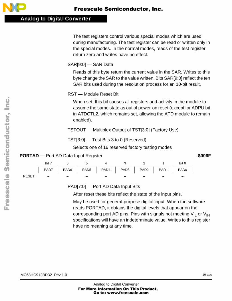
Analog to Digital Converter
F
ree
sca
le S
em
ico
nd
uc
tor,
I
Freescale Semiconductor, Inc.n
c..
.
The test registers control various special modes which are used during manufacturing. The test register can be read or written only in the special modes. In the normal modes, reads of the test register return zero and writes have no effect.
SAR[9:0] — SAR Data
Reads of this byte return the current value in the SAR. Writes to this byte change the SAR to the value written. Bits SAR[9:0] reflect the ten SAR bits used during the resolution process for an 10-bit result.
RST — Module Reset Bit
When set, this bit causes all registers and activity in the module to assume the same state as out of power-on reset (except for ADPU bit in ATDCTL2, which remains set, allowing the ATD module to remain enabled).
TSTOUT — Multiplex Output of TST[3:0] (Factory Use)
TST[3:0] — Test Bits 3 to 0 (Reserved)
Selects one of 16 reserved factory testing modes
PAD[7:0] — Port AD Data Input Bits
After reset these bits reflect the state of the input pins.
May be used for general-purpose digital input. When the software reads PORTAD, it obtains the digital levels that appear on the corresponding port AD pins. Pins with signals not meeting VIL or VIH specifications will have an indeterminate value. Writes to this register have no meaning at any time.
PORTAD — Port AD Data Input Register $006F
Bit 7 6 5 4 3 2 1 Bit 0
PAD7 PAD6 PAD5 PAD4 PAD3 PAD2 PAD1 PAD0
RESET: – – – – – – – –
MC68HC912BD32 Rev 1.0
Analog to Digital Converter For More Information On This Prod
Go to: www.freescale.com
10-adc
uct,
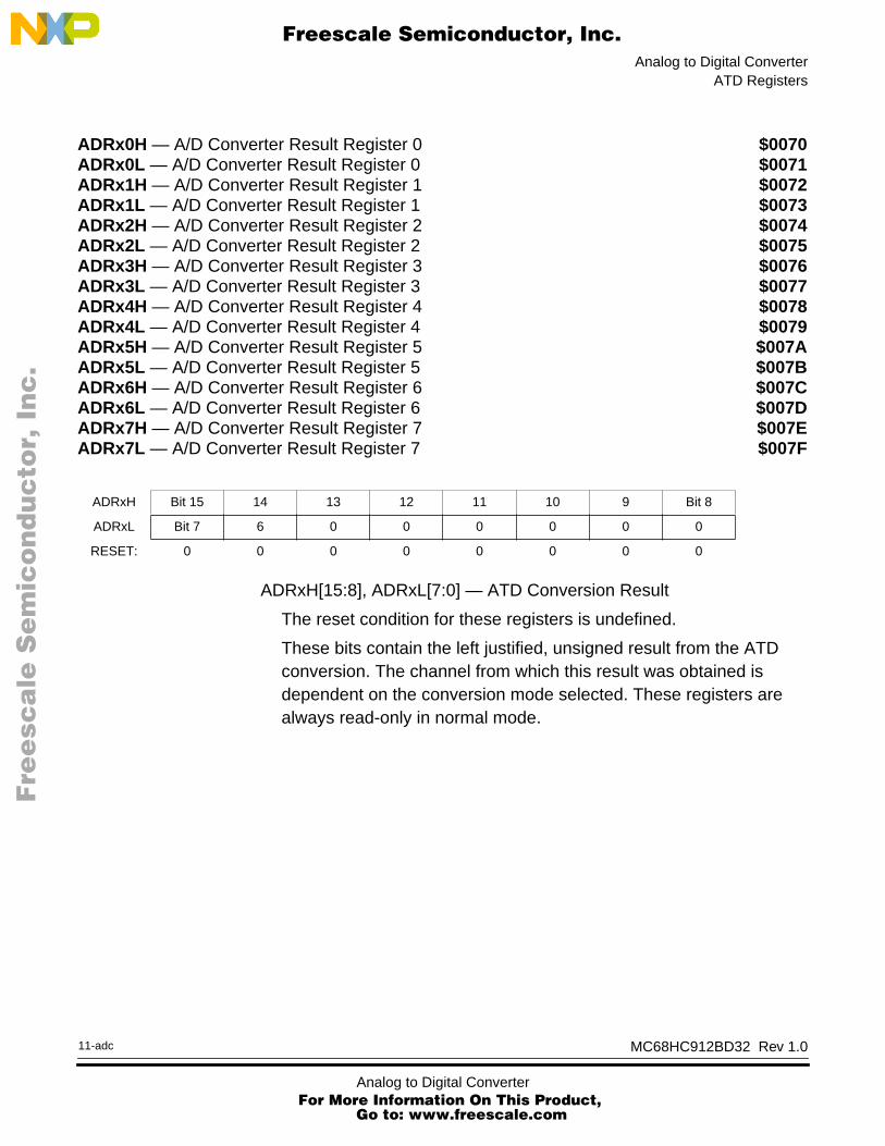
Analog to Digital ConverterATD Registers
MC68HC912BD32 Rev 1.0
F
ree
sca
le S
em
ico
nd
uc
tor,
I
Freescale Semiconductor, Inc.n
c..
.
11-adc
ADRxH[15:8], ADRxL[7:0] — ATD Conversion Result
The reset condition for these registers is undefined.
These bits contain the left justified, unsigned result from the ATD conversion. The channel from which this result was obtained is dependent on the conversion mode selected. These registers are always read-only in normal mode.
ADRx0H — A/D Converter Result Register 0 $0070ADRx0L — A/D Converter Result Register 0 $0071ADRx1H — A/D Converter Result Register 1 $0072ADRx1L — A/D Converter Result Register 1 $0073ADRx2H — A/D Converter Result Register 2 $0074ADRx2L — A/D Converter Result Register 2 $0075ADRx3H — A/D Converter Result Register 3 $0076ADRx3L — A/D Converter Result Register 3 $0077ADRx4H — A/D Converter Result Register 4 $0078ADRx4L — A/D Converter Result Register 4 $0079ADRx5H — A/D Converter Result Register 5 $007AADRx5L — A/D Converter Result Register 5 $007BADRx6H — A/D Converter Result Register 6 $007CADRx6L — A/D Converter Result Register 6 $007DADRx7H — A/D Converter Result Register 7 $007EADRx7L — A/D Converter Result Register 7 $007F
ADRxH Bit 15 14 13 12 11 10 9 Bit 8
ADRxL Bit 7 6 0 0 0 0 0 0
RESET: 0 0 0 0 0 0 0 0
Analog to Digital Converter For More Information On This Product,
Go to: www.freescale.com

Analog to Digital Converter
F
ree
sca
le S
em
ico
nd
uc
tor,
I
Freescale Semiconductor, Inc.n
c..
.
ATD Mode Operation
STOP — causes all clocks to halt (if the S bit in the CCR is zero). The system is placed in a minimum-power standby mode. This aborts any conversion sequence in progress. During STOP recovery, the ATD must delay for the STOP recovery time (tSR) before initiating a new ATD conversion sequence.
WAIT — ATD conversion continues unless AWAI bit in ATDCTL2 register is set.
BDM — Debug options available as set in register ATDCTL3.
USER — ATD continues running unless ADPU is cleared.
ADPU — ATD operations are stopped if ADPU = 0, but registers are accessible.
MC68HC912BD32 Rev 1.0
Analog to Digital Converter For More Information On This Prod
Go to: www.freescale.com
12-adc
uct,
F
ree
sca
le S
em
ico
nd
uc
tor,
IFreescale Semiconductor, Inc.
nc
...
Development SupportDevelopment Support
Contents
Introduction . . . . . . . . . . . . . . . . . . . . . . . . . . . . . . . . . . . . . . . . . . . . 231Instruction Queue . . . . . . . . . . . . . . . . . . . . . . . . . . . . . . . . . . . . . . . 231Background Debug Mode . . . . . . . . . . . . . . . . . . . . . . . . . . . . . . . . . 233Breakpoints . . . . . . . . . . . . . . . . . . . . . . . . . . . . . . . . . . . . . . . . . . . . 247Instruction Tagging . . . . . . . . . . . . . . . . . . . . . . . . . . . . . . . . . . . . . . 253
Introduction
Development support involves complex interactions between MC68HC912BD32 resources and external development systems. The following section concerns instruction queue and queue tracking signals, background debug mode, and instruction tagging.
Instruction Queue
The CPU12 instruction queue provides at least three bytes of program information to the CPU when instruction execution begins. The CPU12 always completely finishes executing an instruction before beginning to execute the next instruction. Status signals IPIPE[1:0] provide information about data movement in the queue and indicate when the CPU begins to execute instructions. This makes it possible to monitor CPU activity on a cycle-by-cycle basis for debugging. Information available on the IPIPE[1:0] pins is time multiplexed. External circuitry can latch data movement information on rising edges of the E-clock signal; execution start information can be latched on falling edges. Table 55 shows the meaning of data on the pins.
MC68HC912BD32 Rev 1.0
1-devDevelopment Support For More Information On This Product,
Go to: www.freescale.com
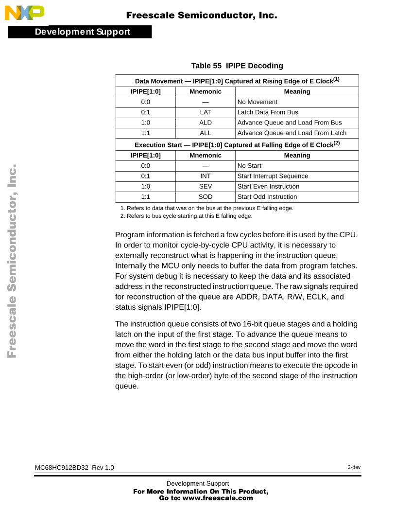
Development Support
F
ree
sca
le S
em
ico
nd
uc
tor,
I
Freescale Semiconductor, Inc.n
c..
.
Program information is fetched a few cycles before it is used by the CPU. In order to monitor cycle-by-cycle CPU activity, it is necessary to externally reconstruct what is happening in the instruction queue. Internally the MCU only needs to buffer the data from program fetches. For system debug it is necessary to keep the data and its associated address in the reconstructed instruction queue. The raw signals required for reconstruction of the queue are ADDR, DATA, R/W, ECLK, and status signals IPIPE[1:0].
The instruction queue consists of two 16-bit queue stages and a holding latch on the input of the first stage. To advance the queue means to move the word in the first stage to the second stage and move the word from either the holding latch or the data bus input buffer into the first stage. To start even (or odd) instruction means to execute the opcode in the high-order (or low-order) byte of the second stage of the instruction queue.
Table 55 IPIPE Decoding
Data Movement — IPIPE[1:0] Captured at Rising Edge of E Clock (1)
1. Refers to data that was on the bus at the previous E falling edge.
IPIPE[1:0] Mnemonic Meaning
0:0 — No Movement
0:1 LAT Latch Data From Bus
1:0 ALD Advance Queue and Load From Bus
1:1 ALL Advance Queue and Load From Latch
Execution Start — IPIPE[1:0] Captured at Falling Edge of E Clock (2)
2. Refers to bus cycle starting at this E falling edge.
IPIPE[1:0] Mnemonic Meaning
0:0 — No Start
0:1 INT Start Interrupt Sequence
1:0 SEV Start Even Instruction
1:1 SOD Start Odd Instruction
MC68HC912BD32 Rev 1.0
Development Support For More Information On This Prod
Go to: www.freescale.com
2-dev
uct,
Development SupportBackground Debug Mode
F
ree
sca
le S
em
ico
nd
uc
tor,
I
Freescale Semiconductor, Inc.n
c..
.
Background Debug Mode
Background debug mode (BDM) is used for system development, in-circuit testing, field testing, and programming. BDM is implemented in on-chip hardware and provides a full set of debug options.
Because BDM control logic does not reside in the CPU, BDM hardware commands can be executed while the CPU is operating normally. The control logic generally uses CPU dead cycles to execute these commands, but can steal cycles from the CPU when necessary. Other BDM commands are firmware based, and require the CPU to be in active background mode for execution. While BDM is active, the CPU executes a firmware program located in a small on-chip ROM that is available in the standard 64-Kbyte memory map only while BDM is active.
The BDM control logic communicates with an external host development system serially, via the BKGD pin. This single-wire approach minimizes the number of pins needed for development support.
Enabling BDM Firmware Commands
BDM is available in all operating modes, but must be made active before firmware commands can be executed. BDM is enabled by setting the ENBDM bit in the BDM STATUS register via the single wire interface (using a hardware command; WRITE_BD_BYTE at $FF01). BDM must then be activated to map BDM registers and ROM to addresses $FF00 to $FFFF and to put the MCU in active background mode.
After the firmware is enabled, BDM can be activated by the hardware BACKGROUND command, by the BDM tagging mechanism, or by the CPU BGND instruction. An attempt to activate BDM before firmware has been enabled causes the MCU to resume normal instruction execution after a brief delay.
BDM becomes active at the next instruction boundary following execution of the BDM BACKGROUND command, but tags activate BDM before a tagged instruction is executed.
MC68HC912BD32 Rev 1.0
3-devDevelopment Support For More Information On This Product,
Go to: www.freescale.com

Development Support
F
ree
sca
le S
em
ico
nd
uc
tor,
I
Freescale Semiconductor, Inc.n
c..
.
In special single-chip mode, background operation is enabled and active immediately out of reset. This active case replaces the M68HC11 boot function, and allows programming a system with blank memory.
While BDM is active, a set of BDM control registers are mapped to addresses $FF00 to $FF06. The BDM control logic uses these registers which can be read anytime by BDM logic, not user programs. Refer to BDM Registers for detailed descriptions.
Some on-chip peripherals have a BDM control bit which allows suspending the peripheral function during BDM. For example, if the timer control is enabled, the timer counter is stopped while in BDM. Once normal program flow is continued, the timer counter is re-enabled to simulate real-time operations.
BDM Serial Interface
The BDM serial interface requires the external controller to generate a falling edge on the BKGD pin to indicate the start of each bit time. The external controller provides this falling edge whether data is transmitted or received.
BKGD is a pseudo-open-drain pin that can be driven either by an external controller or by the MCU. Data is transferred MSB first at 16 B-clock cycles per bit (nominal speed). The interface times out if 512 B-clock cycles occur between falling edges from the host. The hardware clears the command register when a time-out occurs.
The BKGD pin can receive a high or low level or transmit a high or low level. The following diagrams show timing for each of these cases. Interface timing is synchronous to MCU clocks but asynchronous to the external host. The internal clock signal is shown for reference in counting cycles.
Figure 56 shows an external host transmitting a logic one or zero to the BKGD pin of a target MC68HC912BD32 MCU. The host is asynchronous to the target so there is a 0-to-1 cycle delay from the host-generated falling edge to where the target perceives the beginning of the bit time. Ten target B cycles later, the target senses the bit level on the BKGD pin. Typically the host actively drives the pseudo-open-drain BKGD pin during host-to-target transmissions to
MC68HC912BD32 Rev 1.0
Development Support For More Information On This Prod
Go to: www.freescale.com
4-dev
uct,

Development SupportBackground Debug Mode
F
ree
sca
le S
em
ico
nd
uc
tor,
I
Freescale Semiconductor, Inc.n
c..
.
speed up rising edges. Since the target does not drive the BKGD pin during this period, there is no need to treat the line as an open-drain signal during host-to-target transmissions.
Figure 56 BDM Host to Target Serial Bit Timing
Figure 57 BDM Target to Host Serial Bit Timing (Logic 1)
10 CYCLES
B CLOCK(TARGET MCU)
HOSTTRANSMIT 1
TARGET SENSES BIT
EARLIESTSTART OFNEXT BITSYNCHRONIZATION
UNCERTAINTY
PERCEIVEDSTART
OF BIT TIME
HOSTTRANSMIT 0
10 CYCLES
B CLOCK(TARGET
MCU)
EARLIESTSTART OFNEXT BIT
BKGD PIN
PERCEIVEDSTART OF BIT
TIME
10 CYCLES
HOST SAMPLESBKGD PIN
HOSTDRIVE TOBKGD PIN
TARGET MCUSPEEDUP PULSE
R-C RISE
HIGH-IMPEDANCE
HIGH-IMPEDANCE
HIGH-IMPEDANCE
MC68HC912BD32 Rev 1.0
5-devDevelopment Support For More Information On This Product,
Go to: www.freescale.com
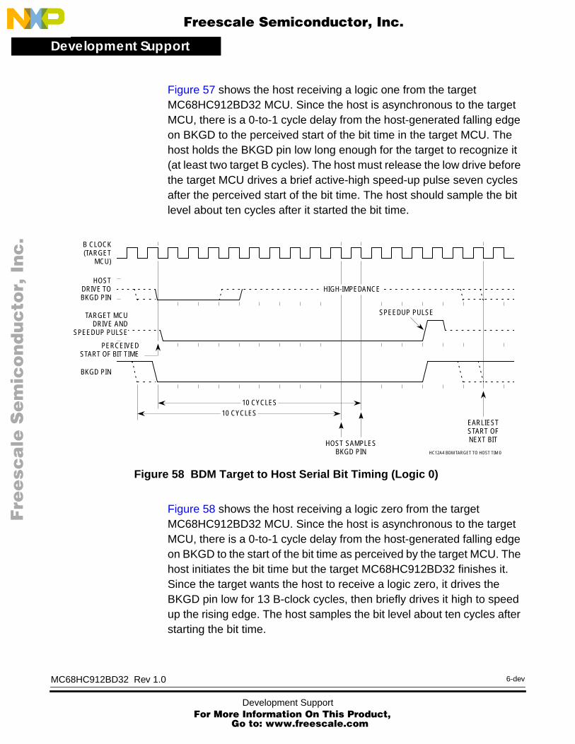
Development Support
F
ree
sca
le S
em
ico
nd
uc
tor,
I
Freescale Semiconductor, Inc.n
c..
.
Figure 57 shows the host receiving a logic one from the target MC68HC912BD32 MCU. Since the host is asynchronous to the target MCU, there is a 0-to-1 cycle delay from the host-generated falling edge on BKGD to the perceived start of the bit time in the target MCU. The host holds the BKGD pin low long enough for the target to recognize it (at least two target B cycles). The host must release the low drive before the target MCU drives a brief active-high speed-up pulse seven cycles after the perceived start of the bit time. The host should sample the bit level about ten cycles after it started the bit time.
Figure 58 BDM Target to Host Serial Bit Timing (Logic 0)
Figure 58 shows the host receiving a logic zero from the target MC68HC912BD32 MCU. Since the host is asynchronous to the target MCU, there is a 0-to-1 cycle delay from the host-generated falling edge on BKGD to the start of the bit time as perceived by the target MCU. The host initiates the bit time but the target MC68HC912BD32 finishes it. Since the target wants the host to receive a logic zero, it drives the BKGD pin low for 13 B-clock cycles, then briefly drives it high to speed up the rising edge. The host samples the bit level about ten cycles after starting the bit time.
10 CYCLES
B CLOCK(TARGET
MCU)
EARLIESTSTART OFNEXT BIT
BKGD PIN
PERCEIVEDSTART OF BIT TIME
10 CYCLES
HOST SAMPLESBKGD PIN
HOSTDRIVE TOBKGD PIN
TARGET MCUDRIVE AND
SPEEDUP PULSE
HIGH-IMPEDANCE
SPEEDUP PULSE
HC12A4 BDM TARGET TO HOST TIM 0
MC68HC912BD32 Rev 1.0
Development Support For More Information On This Prod
Go to: www.freescale.com
6-dev
uct,

Development SupportBackground Debug Mode
MC68HC912BD32 Rev 1.0
F
ree
sca
le S
em
ico
nd
uc
tor,
I
Freescale Semiconductor, Inc.n
c..
.
7-dev
BDM Commands The BDM command set consists of two types: hardware and firmware. Hardware commands allow target system memory to be read or written.Target system memory includes all memory that is accessible by the CPU12 including EEPROM, on-chip I/O and control registers, and external memory that is connected to the target HC12 MCU.Hardware commands are implemented in hardware logic and do not require the HC12 MCU to be in BDM mode for execution.The control logic watches the CPU12 buses to find a free bus cycle to execute the command so the background access does not disturb the running application programs. If a free cycle is not found within 128 B-clock cycles, the CPU12 is momentarily frozen so the control logic can steal a cycle.Commands implemented in BDM control logic are listed in Table 56.
Table 56 Hardware Commands (1)
Command Opcode (Hex) Data Description
BACKGROUND 90 None Enter background mode if firmware enabled.
READ_BD_BYTE(1) E416-bit address16-bit data out
Read from memory with BDM in map (may steal cycles if external access) data for odd address on low byte, data for even address on high byte.
READ_BD_WORD(1) EC16-bit address 16-bit data out
Read from memory with BDM in map (may steal cycles if external access). Must be aligned access.
READ_BYTE E016-bit address16-bit data out
Read from memory with BDM out of map (may steal cycles if external access) data for odd address on low byte, data for even address on high byte.
READ_WORD E816-bit address16-bit data out
Read from memory with BDM out of map (may steal cycles if external access). Must be aligned access.
WRITE_BD_BYTE(1) C416-bit address 16-bit data in
Write to memory with BDM in map (may steal cycles if external access) data for odd address on low byte, data for even address on high byte.
WRITE_BD_WORD(1) CC16-bit address 16-bit data in
Write to memory with BDM in map (may steal cycles if external access). Must be aligned access.
WRITE_BYTE C016-bit address 16-bit data in
Write to memory with BDM out of map (may steal cycles if external access) data for odd address on low byte, data for even address on high byte.
WRITE_WORD C816-bit address 16-bit data in
Write to memory with BDM out of map (may steal cycles if external access). Must be aligned access.
1. Use these commands only for reading/writing to BDM locations.The BDM firmware ROM and BDM registers are not normallyin the HC12 MCU memory map.Since these locations have the same addresses as some of the normal application memorymap, there needs to be a way to decide which physical locations are being accessed by the hardware BDM commands.Thisgives rise to needing separate memory access commands for the BDM locations as opposed to the normal application loca-tions.In logic, this is accomplished by momentarily enabling the BDM memory resources, just for the access cycles of theREAD_BD and WRITE_BD commands.This logic allows the debugging system to unobtrusively access the BDM locationseven if the application program is running out of the same memory area in the normal application memory map.
Development Support For More Information On This Product,
Go to: www.freescale.com

Development Support
F
ree
sca
le S
em
ico
nd
uc
tor,
I
Freescale Semiconductor, Inc.n
c..
.
The second type of BDM commands are called firmware commands implemented in a small ROM within the HC12 MCU.The CPU must be in background mode to execute firmware commands. The usual way to get to background mode is by the hardware command BACKGROUND. The BDM ROM is located at $FF20 to $FFFF while BDM is active. There are also seven bytes of BDM registers located at $FF00 to $FF06 while BDM is active. The CPU executes code in the BDM firmware to perform the requested operation. The BDM firmware watches for serial commands and executes them as they are received. The firmware commands are shown in Table 57.
Each of the hardware and firmware BDM commands start with an 8-bit command code (opcode). Depending upon the commands, a 16-bit address and/or a 16-bit data word is required as indicated in the tables by the command. All the read commands output 16-bits of data despite the byte/word implication in the command name.
The external host should wait 150 BCLK cycles for a non-intrusive BDM command to execute before another command is sent. This delay includes 128 BCLK cycles for the maximum delay for a free cycle.For
Table 57 BDM Firmware Commands
Command Opcode (Hex) Data Description
READ_NEXT 62 16-bit data out X = X + 2; Read next word pointed to by X
READ_PC 63 16-bit data out Read program counter
READ_D 64 16-bit data out Read D accumulator
READ_X 65 16-bit data out Read X index register
READ_Y 66 16-bit data out Read Y index register
READ_SP 67 16-bit data out Read stack pointer
WRITE_NEXT 42 16-bit data in X = X + 2; Write next word pointed to by X
WRITE_PC 43 16-bit data in Write program counter
WRITE_D 44 16-bit data in Write D accumulator
WRITE_X 45 16-bit data in Write X index register
WRITE_Y 46 16-bit data in Write Y index register
WRITE_SP 47 16-bit data in Write stack pointer
GO 08 None Go to user program
TRACE1 10 None Execute one user instruction then return to BDM
TAGGO 18 None Enable tagging and go to user program
MC68HC912BD32 Rev 1.0
Development Support For More Information On This Prod
Go to: www.freescale.com
8-dev
uct,

Development SupportBackground Debug Mode
MC68HC912BD32 Rev 1.0
F
ree
sca
le S
em
ico
nd
uc
tor,
I
Freescale Semiconductor, Inc.n
c..
.
9-dev
data read commands, the host must insert this delay between sending the address and attempting to read the data.In the case of a write command, the host must delay after the data portion, before sending a new command, to be sure the write has finished.
The external host should delay about 32 target BCLK cycles between a firmware read command and the data portion of these commands. This allows the BDM firmware to execute the instructions needed to get the requested data into the BDM SHIFTER register.
The external host should delay about 32 target BCLK cycles after the data portion of firmware write commands to allow BDM firmware to complete the requested write operation before a new serial command disturbs the BDM SHIFTER register.
The external host should delay about 64 target BCLK cycles after a TRACE1 or GO command before starting any new serial command. This delay is needed because the BDM SHIFTER register is used as a temporary data holding register during the exit sequence to user code.
BDM logic retains control of the internal buses until a read or write is completed.If an operation can be completed in a single cycle, it does not intrude on normal CPU12 operation.However, if an operation requires multiple cycles, CPU12 clocks are frozen until the operation is complete.
BDM Lockout The access to the MCU resources by BDM may be prevented by enabling the BDM lockout feature. When enabled, the BDM lockout mechanism prevents the BDM from being active. In this case the BDM ROM is disabled and does not appear in the MCU memory map.
The BDM lockout is enabled by clearing NOBDML bit of EEMCR register. The NOBDML bit is loaded at reset from the SHADOW byte of EEPROM module. Modifying the state of the NOBDML and corresponding EEPROM SHADOW bit is only possible in special modes.
Please refer to EEPROM for NOBDML information.
Development Support For More Information On This Product,
Go to: www.freescale.com

Development Support
F
ree
sca
le S
em
ico
nd
uc
tor,
I
Freescale Semiconductor, Inc.n
c..
.
Enabling the BDM lockout
Enabling the BDM lockout feature is only possible in special modes (SMODN=0) and is accomplished by the following steps.
1. Remove the SHADOW byte protection by clearing SHPROT bit in EEPROT register.
2. Clear NOSHB bit in EEMCR register to make the SHADOW byte visible at $0FC0.
3. Program bit 7 of the SHADOW byte like a regular EEPROM location at address $0FC0 (write $7F into address $0FC0). Do not program other bits of the SHADOW byte (location $0FC0); otherwise some regular EEPROM array locations will not be visible. At the next reset, the SHADOW byte is loaded into the EEMCR register. NOBDML bit in EEMCR will be cleared and BDM will not be operational.
4. Protect the SHADOW byte by setting SHPROT bit in EEPROT register.
Disabling the BDM lockout
Disabling the BDM lockout is only possible in special modes (SMODN=0). Follow the same steps as for enabling the BDM lockout, but erase the SHADOW byte.
At the next reset, the SHADOW byte is loaded into the EEMCR register. NOBDML bit in EEMCR will be set and BDM becomes operational.
BDM Registers Seven BDM registers are mapped into the standard 64-Kbyte address space when BDM is active. Mapping is shown in Table 58.
Table 58 BDM registers
Address Register
$FF00 BDM Instruction Register
$FF01 BDM Status Register
$FF02 – $FF03 BDM Shift Register
$FF04 – $FF05 BDM Address Register
$FF06 BDM CCR Holding Register
MC68HC912BD32 Rev 1.0
Development Support For More Information On This Prod
Go to: www.freescale.com
10-dev
uct,

Development SupportBackground Debug Mode
MC68HC912BD32 Rev 1.0
F
ree
sca
le S
em
ico
nd
uc
tor,
I
Freescale Semiconductor, Inc.n
c..
.
11-dev
The content of the INSTRUCTION register is determined by the type of background command being executed.The STATUS register indicates BDM operating conditions.The SHIFT register contains data being received or transmitted via the serial interface. The ADDRESS register is temporary storage for BDM commands.The CCRSAV register preserves the content of the CPU12 CCR while BDM is active.
The only registers of interest to users are the STATUS register and the CCRSAV register.The other BDM registers are only used by the BDM firmware to execute commands.The registers are accessed by means of the hardware READ_BD and WRITE_BD commands, but should not be written during BDM operation (except the CCRSAV register which could be written to modify the CCR value).
STATUS The STATUS register is read and written by the BDM hardware as a result of serial data shifted in on the BKGD pin.
Read: all modes.
Write: Bits 3 through 5, and bit 7 are writable in all modes. Bit 6, BDMACT, can only be written if bit 7 H/F in the INSTRUCTION register is a zero. Bit 2, CLKSW, can only be written if bit 7 H/F in the INSTRUCTION register is a one. A user would never write ones to bits 3 through 5 because these bits are only used by BDM firmware.
ENBDM — Enable BDM (permit active background debug mode)0 = BDM cannot be made active (hardware commands still
allowed).1 = BDM can be made active to allow firmware commands.
STATUS — BDM Status Register(1) $FF01
BIT 7 6 5 4 3 2 1 BIT 0ENBDM BDMACT ENTAG SDV TRACE CLKSW - -
RESET: 0 (NOTE 1)
1 0 0 0 0 0 0Special
Single Chip & Periph
RESET:0 0 0 0 0 0 0 0 All other
modes
1. ENBDM is set to 1 by the firmware in Special Single Chip mode.
Development Support For More Information On This Product,
Go to: www.freescale.com

Development Support
F
ree
sca
le S
em
ico
nd
uc
tor,
I
Freescale Semiconductor, Inc.n
c..
.
BDMACT — Background Mode Active Status
BDMACT becomes set as active BDM mode is entered so that the BDM firmware ROM is enabled and put into the map. BDMACT is cleared by a carefully timed store instruction in the BDM firmware as part of the exit sequence to return to user code and remove the BDM memory from the map. This bit has 4 clock cycles write delay.
0 = BDM is not active. BDM ROM and registers are not in map.1 = BDM is active and waiting for serial commands. BDM ROM and
registers are in map
CAUTION: The user should be careful that the state of the BDMACT bit is not unintentionally
changed with the WRITE_NEXT firmware command. If it is unintentionally changed
from 1 to 0, it will cause a system runaway because it would disable the BDM firmware
ROM while the CPU12 was executing BDM firmware. The following two commands
show how BDMACT may unintentionally get changed from 1 to 0.
WRITE_X with data $FEFE
WRITE_NEXT with data $C400
The first command writes the data $FEFE to the X index register. The second
command writes the data $C4 to the $FF00 INSTRUCTION register and also writes the
data $00 to the $FF01 STATUS register.
ENTAG — Tagging Enable
Set by the TAGGO command and cleared when BDM mode is entered. The serial system is disabled and the tag function enabled 16 cycles after this bit is written.
0 = Tagging not enabled, or BDM active.1 = Tagging active. BDM cannot process serial commands while
tagging is active.
SDV — Shifter Data Valid
Shows that valid data is in the serial interface shift register. Used by the BDM firmware.
0 = No valid data. Shift operation is not complete.1 = Valid Data. Shift operation is complete.
TRACE — Asserted by the TRACE1 command
MC68HC912BD32 Rev 1.0
Development Support For More Information On This Prod
Go to: www.freescale.com
12-dev
uct,

Development SupportBackground Debug Mode
MC68HC912BD32 Rev 1.0
F
ree
sca
le S
em
ico
nd
uc
tor,
I
Freescale Semiconductor, Inc.n
c..
.
13-dev
CLKSW — Clock Switch0 = BDM system operates with BCLK.1 = BDM system operates with ECLK.
The WRITE_BD_BYTE@FF01 command that changes CLKSW including 150 cycles after the data portion of the command should be timed at the old speed. Beginning with the start of the next BDM command, the new clock can be used for timing BDM communications.
If ECLK rate is slower than BCLK rate, CLKSW is ignored and BDM system is forced to operate with ECLK.
INSTRUCTION – Hardware Instruction Decode
The INSTRUCTION register is written by the BDM hardware as a result of serial data shifted in on the BKGD pin. It is readable and writable in Special Peripheral mode on the parallel bus. It is discussed here for two conditions: when a hardware command is executed and when a firmware command is executed.
Read and write: all modes
. The hardware clears the INSTRUCTION register if 512 BCLK cycles occur between falling edges from the host.
The bits in the BDM instruction register have the following meanings when a hardware command is executed.
H/F — Hardware/Firmware Flag0 = Firmware command1 = Hardware command
DATA — Data Flag – Shows that data accompanies the command.0 = No data1 = Data follows the command
INSTRUCTION — BDM Instruction Register (hardware command explanation) $FF00
BIT 7 6 5 4 3 2 1 BIT 0H/F DATA R/W BKGND W/B BD/U 0 0
RESET: 0 0 0 0 0 0 0 0
Development Support For More Information On This Product,
Go to: www.freescale.com

Development Support
F
ree
sca
le S
em
ico
nd
uc
tor,
I
Freescale Semiconductor, Inc.n
c..
.
R/W — Read/Write Flag0 = Write1 = Read
BKGND — Hardware request to enter active background mode0 = Not a hardware background command1 = Hardware background command (INSTRUCTION = $90)
W/B — Word/Byte Transfer Flag0 = Byte transfer1 = Word transfer
BD/U — BDM Map/User Map Flag
Indicates whether BDM registers and ROM are mapped to addresses $FF00 to $FFFF in the standard 64-Kbyte address space. Used only by hardware read/write commands.
0 = BDM resources not in map1 = BDM ROM and registers in map
The bits in the BDM instruction register have the following meanings when a firmware command is executed.
H/F — Hardware/Firmware Flag0 = Firmware command1 = Hardware command
DATA — Data Flag – Shows that data accompanies the command.0 = No data1 = Data follows the command
R/W — Read/Write Flag0 = Write1 = Read
INSTRUCTION — BDM Instruction Register (firmware command bit explanation) $FF00
Bit 7 6 5 4 3 2 1 Bit 0H/F DATA R/W TTAGO REGN
MC68HC912BD32 Rev 1.0
Development Support For More Information On This Prod
Go to: www.freescale.com
14-dev
uct,

Development SupportBackground Debug Mode
MC68HC912BD32 Rev 1.0
F
ree
sca
le S
em
ico
nd
uc
tor,
I
Freescale Semiconductor, Inc.n
c..
.
15-dev
TTAGO — Trace, Tag, Go Field
REGN — Register/Next Field
Indicates which register is being affected by a command. In the case of a READ_NEXT or WRITE_NEXT command, index register X is pre-incriminated by 2 and the word pointed to by X is then read or written.
Table 59 TTAGO Decoding
TTAGO Value Instruction
00 —
01 GO
10 TRACE1
11 TAGGO
Table 60 REGN Decoding
REGN Value Instruction
000 —
001 —
010 READ/WRITE NEXT
011 PC
100 D
101 X
110 Y
111 SP
Development Support For More Information On This Product,
Go to: www.freescale.com

Development Support
F
ree
sca
le S
em
ico
nd
uc
tor,
I
Freescale Semiconductor, Inc.n
c..
.
SHIFTER This 16-bit shift register contains data being received or transmitted via the serial interface. It is also used by the BDM firmware for temporary storage.
Read: all modes (but not normally accessed by users)
Write: all modes (but not normally accessed by users)
ADDRESS This 16-bit address register is temporary storage for BDM hardware and firmware commands.
Read: all modes (but not normally accessed by users)
Write: only by BDM hardware (state machine)
SHIFTER — BDM Shift Register – High Byte $FF02
BIT 15 14 13 12 11 10 9 BIT 8S15 S14 S13 S12 S11 S10 S9 S8
RESET: X X X X X X X X
SHIFTER — BDM Shift Register – Low Byte $FF03
BIT 7 6 5 4 3 2 1 BIT 0S7 S6 S5 S4 S3 S2 S1 S0
RESET: X X X X X X X X
ADDRESS — BDM Address Register – High Byte $FF04
BIT 15 14 13 12 11 10 9 BIT 8A15 A14 A13 A12 A11 A10 A9 A8
RESET: X X X X X X X X
ADDRESS — BDM Address Register – High Byte $FF05
BIT 7 6 5 4 3 2 1 BIT 0A7 A6 A5 A4 A3 A2 A1 A0
RESET: X X X X X X X X
MC68HC912BD32 Rev 1.0
Development Support For More Information On This Prod
Go to: www.freescale.com
16-dev
uct,

Development SupportBreakpoints
MC68HC912BD32 Rev 1.0
F
ree
sca
le S
em
ico
nd
uc
tor,
I
Freescale Semiconductor, Inc.n
c..
.
17-dev
CCRSAV The CCRSAV register is used to save the CCR of the users program when entering BDM. It is also used for temporary storage in the BDM firmware.
Read and write: all modes
Breakpoints
Hardware breakpoints are used to debug software on the MC68HC912BD32 by comparing actual address and data values to predetermined data in setup registers. A successful comparison will place the CPU in background debug mode (BDM) or initiate a software interrupt (SWI). Breakpoint features designed into the BDM256 include:
• Mode selection for BDM or SWI generation
• Program fetch tagging for cycle of execution breakpoint
• Second address compare in dual address modes
• Range compare by disable of low byte address
• Data compare in full feature mode for non-tagged breakpoint
• Byte masking for high/low byte data compares
• R/W compare for non-tagged compares
• Tag inhibit on BDM TRACE
CCRSAV — BDM CCR Holding Register $FF06
BIT 7 6 5 4 3 2 1 BIT 0CCR7 CCR6 CCR5 CCR4 CCR3 CCR2 CCR1 CCR0
RESET: NOTE 1 (1) X X X X X X X X
1. Initialized to equal the CPU12 CCR register by the firmware.
Development Support For More Information On This Product,
Go to: www.freescale.com

Development Support
F
ree
sca
le S
em
ico
nd
uc
tor,
I
Freescale Semiconductor, Inc.n
c..
.
Breakpoint Modes Three modes of operation determine the type of breakpoint in effect.
• Dual address-only breakpoints, each of which will cause a software interrupt (SWI)
• Single full-feature breakpoint which will cause the part to enter background debug mode (BDM)
• Dual address-only breakpoints, each of which will cause the part to enter BDM
Breakpoints will not occur when BDM is active.
SWI Dual Address Mode
In this mode, dual address-only breakpoints can be set, each of which cause a software interrupt. This is the only breakpoint mode which can force the CPU to execute a SWI. Program fetch tagging is the default in this mode; data breakpoints are not possible. In the dual mode each address breakpoint is affected by the BKPM bit and the BKALE bit. The BKxRW and BKxRWE bits are ignored. In dual address mode the BKDBE becomes an enable for the second address breakpoint. The BKSZ8 bit will have no effect when in a dual address mode.
BDM Full Breakpoint Mode
A single full feature breakpoint which causes the part to enter background debug mode. BDM mode may be entered by a breakpoint only if an internal signal from the BDM indicates background debug mode is enabled.
• Breakpoints are not allowed if the BDM mode is already active. Active mode means the CPU is executing out of the BDM ROM.
• BDM should not be entered from a breakpoint unless the ENABLE bit is set in the BDM. This is important because even if the ENABLE bit in the BDM is negated the CPU actually does execute the BDM ROM code. It checks the ENABLE and returns if not set. If the BDM is not serviced by the monitor then the breakpoint would be re-asserted when the BDM returns to normal CPU flow.
• There is no hardware to enforce restriction of breakpoint operation if the BDM is not enabled.
MC68HC912BD32 Rev 1.0
Development Support For More Information On This Prod
Go to: www.freescale.com
18-dev
uct,

Development SupportBreakpoints
MC68HC912BD32 Rev 1.0
F
ree
sca
le S
em
ico
nd
uc
tor,
I
Freescale Semiconductor, Inc.n
c..
.
19-dev
BDM Dual Address Mode
Dual address-only breakpoints, each of which cause the part to enter background debug mode. In the dual mode each address breakpoint is affected, consistent across modes, by the BKPM bit, the BKALE bit, and the BKxRW and BKxRWE bits. In dual address mode the BKDBE becomes an enable for the second address breakpoint. The BKSZ8 bit will have no effect when in a dual address mode. BDM mode may be entered by a breakpoint only if an internal signal from the BDM indicates background debug mode is enabled.
• BKDBE will be used as an enable for the second address only breakpoint.
• Breakpoints are not allowed if the BDM mode is already active. Active mode means the CPU is executing out of the BDM ROM.
• BDM should not be entered from a breakpoint unless the ENABLE bit is set in the BDM. This is important because even if the ENABLE bit in the BDM is negated the CPU actually does execute the BDM ROM code. It checks the ENABLE and returns if not set. If the BDM is not serviced by the monitor then the breakpoint would be re-asserted when the BDM returns to normal CPU flow. There is no hardware to enforce restriction of breakpoint operation if the BDM is not enabled.
Breakpoint Registers
Breakpoint operation consists of comparing data in the breakpoint address registers (BRKAH/BRKAL) to the address bus and comparing data in the breakpoint data registers (BRKDH/BRKDL) to the data bus. The breakpoint data registers can also be compared to the address bus. The scope of comparison can be expanded by ignoring the least significant byte of address or data matches.
The scope of comparison can be limited to program data only by setting the BKPM bit in breakpoint control register 0.
To trace program flow, setting the BKPM bit causes address comparison of program data only. Control bits are also available that allow checking read/write matches.
Development Support For More Information On This Product,
Go to: www.freescale.com
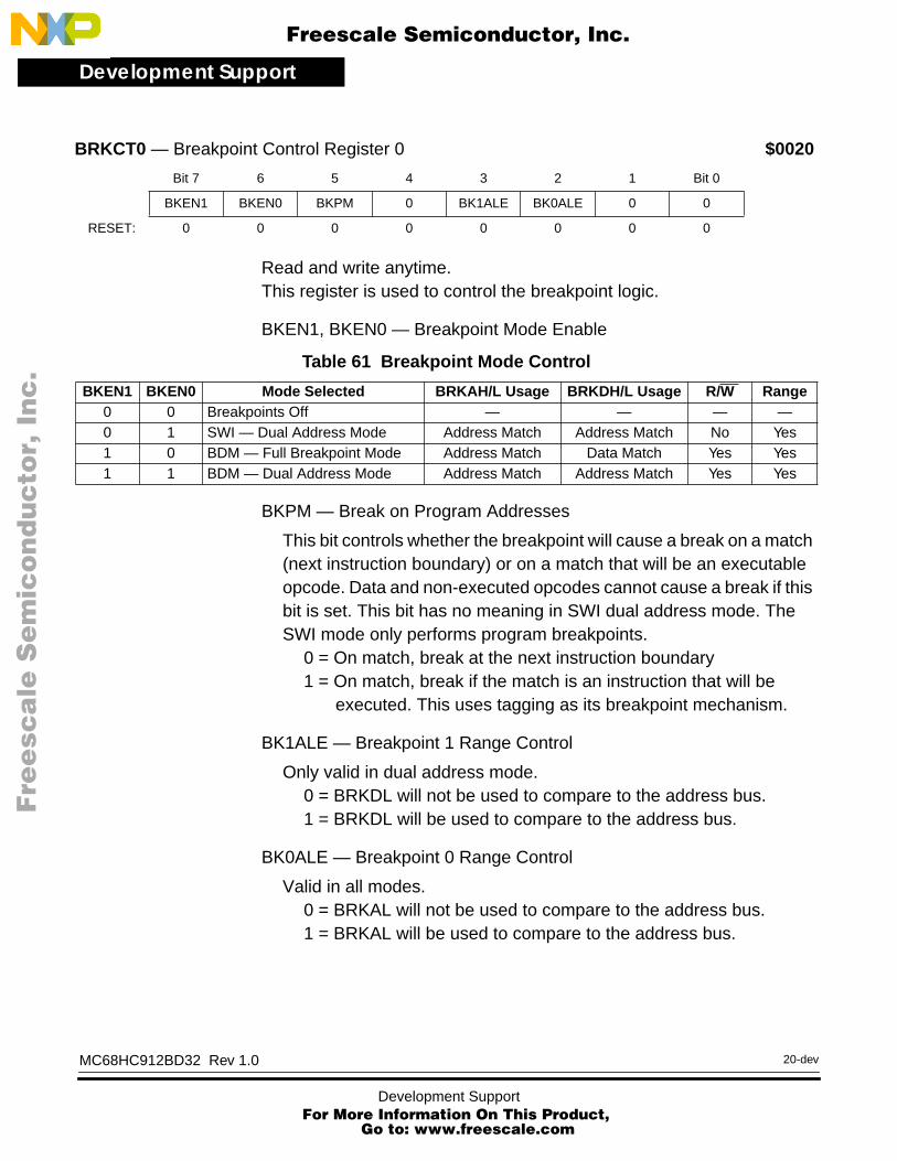
Development Support
F
ree
sca
le S
em
ico
nd
uc
tor,
I
Freescale Semiconductor, Inc.n
c..
.
Read and write anytime.This register is used to control the breakpoint logic.
BKEN1, BKEN0 — Breakpoint Mode Enable
BKPM — Break on Program Addresses
This bit controls whether the breakpoint will cause a break on a match (next instruction boundary) or on a match that will be an executable opcode. Data and non-executed opcodes cannot cause a break if this bit is set. This bit has no meaning in SWI dual address mode. The SWI mode only performs program breakpoints.
0 = On match, break at the next instruction boundary1 = On match, break if the match is an instruction that will be
executed. This uses tagging as its breakpoint mechanism.
BK1ALE — Breakpoint 1 Range Control
Only valid in dual address mode.0 = BRKDL will not be used to compare to the address bus.1 = BRKDL will be used to compare to the address bus.
BK0ALE — Breakpoint 0 Range Control
Valid in all modes.0 = BRKAL will not be used to compare to the address bus.1 = BRKAL will be used to compare to the address bus.
BRKCT0 — Breakpoint Control Register 0 $0020
Bit 7 6 5 4 3 2 1 Bit 0
BKEN1 BKEN0 BKPM 0 BK1ALE BK0ALE 0 0
RESET: 0 0 0 0 0 0 0 0
Table 61 Breakpoint Mode Control
BKEN1 BKEN0 Mode Selected BRKAH/L Usage BRKDH/L Usage R/W Range0 0 Breakpoints Off — — — —0 1 SWI — Dual Address Mode Address Match Address Match No Yes1 0 BDM — Full Breakpoint Mode Address Match Data Match Yes Yes1 1 BDM — Dual Address Mode Address Match Address Match Yes Yes
MC68HC912BD32 Rev 1.0
Development Support For More Information On This Prod
Go to: www.freescale.com
20-dev
uct,

Development SupportBreakpoints
MC68HC912BD32 Rev 1.0
F
ree
sca
le S
em
ico
nd
uc
tor,
I
Freescale Semiconductor, Inc.n
c..
.
21-dev
This register is read/write in all modes.
BKDBE — Enable Data Bus
Enables comparing of address or data bus values using the BRKDH/L registers.
0 = The BRKDH/L registers are not used in any comparison1 = The BRKDH/L registers are used to compare address or data
(depending upon the mode selections BKEN1,0)
BKMBH — Breakpoint Mask High
Disables the comparing of the high byte of data when in full breakpoint mode. Used in conjunction with the BKDBE bit (which should be set)
0 = High byte of data bus (bits 15:8) are compared to BRKDH1 = High byte is not used to in comparisons
BKMBL — Breakpoint Mask Low
Disables the matching of the low byte of data when in full breakpoint mode. Used in conjunction with the BKDBE bit (which should be set)
0 = Low byte of data bus (bits 7:0) are compared to BRKDL1 = Low byte is not used to in comparisons.
BK1RWE — R/W Compare Enable
Enables the comparison of the R/W signal to further specify what causes a match. This bit is NOT useful in program breakpoints or in full breakpoint mode. This bit is used in conjunction with a second address in dual address mode when BKDBE=1.
0 = R/W is not used in comparisons
Table 62 Breakpoint Address Range Control
BK1ALE BK0ALE Address Range Selected– 0 Upper 8-bit address only for full mode or dual mode BKP0– 1 Full 16-bit address for full mode or dual mode BKP00 – Upper 8-bit address only for dual mode BKP11 – Full 16-bit address for dual mode BKP1
BRKCT1 — Breakpoint Control Register 1 $0021
Bit 7 6 5 4 3 2 1 Bit 0
0 BKDBE BKMBH BKMBL BK1RWE BK1RW BK0RWE BK0RW
RESET: 0 0 0 0 0 0 0 0
Development Support For More Information On This Product,
Go to: www.freescale.com

Development Support
F
ree
sca
le S
em
ico
nd
uc
tor,
I
Freescale Semiconductor, Inc.n
c..
.
1 = R/W is used in comparisons
BK1RW — R/W Compare Value
When BK1RWE = 1, this bit determines the type of bus cycle to match.
0 = A write cycle will be matched1 = A read cycle will be matched
BK0RWE — R/W Compare Enable
Enables the comparison of the R/W signal to further specify what causes a match. This bit is not useful in program breakpoints.
0 = R/W is not used in the comparisons1 = R/W is used in comparisons
BK0RW — R/W Compare Value
When BK0RWE = 1, this bit determines the type of bus cycle to match on.
0 = Write cycle will be matched1 = Read cycle will be matched
These bits are used to compare against the most significant byte of the address bus.
Table 63 Breakpoint Read/Write Control
BK1RWE BK1RW BK0RWE BK0RW Read/Write Selected
– – 0 X R/W is don’t care for full mode or dual mode BKP0
– – 1 0 R/W is write for full mode or dual mode BKP0
– – 1 1 R/W is read for full mode or dual mode BKP0
0 X – – R/W is don’t care for dual mode BKP1
1 0 – – R/W is write for dual mode BKP1
1 1 – – R/W is read for dual mode BKP1
BRKAH — Breakpoint Address Register, High Byte $0022
Bit 7 6 5 4 3 2 1 Bit 0
Bit 15 14 13 12 11 10 9 Bit 8
RESET: 0 0 0 0 0 0 0 0
MC68HC912BD32 Rev 1.0
Development Support For More Information On This Prod
Go to: www.freescale.com
22-dev
uct,

Development SupportInstruction Tagging
MC68HC912BD32 Rev 1.0
F
ree
sca
le S
em
ico
nd
uc
tor,
I
Freescale Semiconductor, Inc.n
c..
.
23-dev
These bits are used to compare against the least significant byte of the address bus. These bits may be excluded from being used in the match if BK0ALE = 0.
These bits are compared to the most significant byte of the data bus or the most significant byte of the address bus in dual address modes. BKEN[1:0], BKDBE, and BKMBH control how this byte will be used in the breakpoint comparison.
These bits are compared to the least significant byte of the data bus or the least significant byte of the address bus in dual address modes. BKEN[1:0], BKDBE, BK1ALE, and BKMBL control how this byte will be used in the breakpoint comparison.
Instruction Tagging
The instruction queue and cycle-by-cycle CPU activity can be reconstructed in real time or from trace history that was captured by a logic analyzer. However, the reconstructed queue cannot be used to stop the CPU at a specific instruction, because execution has already
BRKAL — Breakpoint Address Register, Low Byte $0023
Bit 7 6 5 4 3 2 1 Bit 0
Bit 7 6 5 4 3 2 1 Bit 0
RESET: 0 0 0 0 0 0 0 0
BRKDH — Breakpoint Data Register, High Byte $0024
Bit 7 6 5 4 3 2 1 Bit 0
Bit 15 14 13 12 11 10 9 Bit 8
RESET: 0 0 0 0 0 0 0 0
BRKDL — Breakpoint Data Register, Low Byte $0025
Bit 7 6 5 4 3 2 1 Bit 0
Bit 7 6 5 4 3 2 1 Bit 0
RESET: 0 0 0 0 0 0 0 0
Development Support For More Information On This Product,
Go to: www.freescale.com

Development Support
F
ree
sca
le S
em
ico
nd
uc
tor,
I
Freescale Semiconductor, Inc.n
c..
.
begun by the time an operation is visible outside the MCU. A separate instruction tagging mechanism is provided for this purpose.
Executing the BDM TAGGO command configures two MCU pins for tagging. The TAGLO signal shares a pin with the LSTRB signal, and the TAGHI signal shares a pin with the BKGD signal. Tagging information is latched on the falling edge of ECLK.
Table 64 shows the functions of the two tagging pins. The pins operate independently - the state of one pin does not affect the function of the other. The presence of logic level zero on either pin at the fall of ECLK performs the indicated function. Tagging is allowed in all modes. Tagging is disabled when BDM becomes active and BDM serial commands are not processed while tagging is active.
The tag follows program information as it advances through the queue. When a tagged instruction reaches the head of the queue, the CPU enters active background debugging mode rather than execute the instruction.
Table 64 Tag Pin Function
TAGHI TAGLO Tag
1 1 no tag
1 0 low byte
0 1 high byte
0 0 both bytes
MC68HC912BD32 Rev 1.0
Development Support For More Information On This Prod
Go to: www.freescale.com
24-dev
uct,

F
ree
sca
le S
em
ico
nd
uc
tor,
IFreescale Semiconductor, Inc.
nc
...
Preliminary Electrical CharacteristicsPreliminary Electrical Characteristics
This section contains the most accurate electrical information for the MC68HC912BD32 microcontroller available at the time of publication. The information should be considered preliminary and is subject to change. The following characteristics are contained in this document:
Table 65 Maximum Ratings (1)
Rating Symbol Value Unit
Supply voltageVDD, VDDA,
VDDX −0.3 to +6.5 V
Input voltage VIN −0.3 to +6.5 V
Operating temperature rangeMC68HC912BD32FUMC68HC912BD32CFU
TA
TL to TH0 to +70
−40 to +85°C
Storage temperature range Tstg −55 to +150 °C
Current drain per pin(2)
Excluding VDD and VSSIIN ±25 mA
VDD differential voltage VDD−VDDX 6.5 V
1. Permanent damage can occur if maximum ratings are exceeded. Exposures to voltages or currents in excess of recom-mended values affects device reliability. Device modules may not operate normally while being exposed to electrical ex-tremes.
2. One pin at a time, observing maximum power dissipation limits. Internal circuitry protects the inputs against damage causedby high static voltages or electric fields; however, normal precautions are necessary to avoid application of any voltagehigher than maximum-rated voltages to this high-impedance circuit. Extended operation at the maximum ratings can ad-versely affect device reliability. Tying unused inputs to an appropriate logic voltage level (either GND or VDD) enhancesreliability of operation.
MC68HC912BD32 Rev 1.0
1-elecPreliminary Electrical Characteristics For More Information On This Product,
Go to: www.freescale.com

Preliminary Electrical Characteristics
F
ree
sca
le S
em
ico
nd
uc
tor,
I
Freescale Semiconductor, Inc.n
c..
.
Table 66 Thermal Characteristics
Characteristic Symbol Value Unit
Average junction temperature TJ TA + (PD × ΘJA) °C
Ambient temperature TA User-determined °C
Package thermal resistance (junction-to-ambient)80-pin quad flat pack (QFP)
ΘJA 85 °C/W
Total power dissipation(1) PD
PINT + PI/Oor
W
Device internal power dissipation PINT IDD × VDD W
I/O pin power dissipation(2) PI/O User-determined W
A constant(3) KPD × (TA + 273°C) +
ΘJA × PD2
W · °C
1. This is an approximate value, neglecting PI/O.2. For most applications PI/O « PINT and can be neglected.3. K is a constant pertaining to the device. Solve for K with a known TA and a measured PD (at equilibrium). Use this value
of K to solve for PD and TJ iteratively for any value of TA.
KTJ 273°C+--------------------------
MC68HC912BD32 Rev 1.0
Preliminary Electrical Characteristics For More Information On This Prod
Go to: www.freescale.com
2-elec
uct,

Preliminary Electrical Characteristics
F
ree
sca
le S
em
ico
nd
uc
tor,
I
Freescale Semiconductor, Inc.n
c..
.
Table 67 DC Electrical Characteristics
VDD = 5.0 Vdc ±5%, VSS = 0 Vdc, TA = TL to TH, unless otherwise noted
Characteristic Symbol Min Max Unit
Input high voltage, all inputs VIH 0.7 × VDD VDD + 0.3 V
Input low voltage, all inputs VIL VSS−0.3 0.2 × VDD V
Output high voltage, all I/O and output pins except XTALNormal drive strengthIOH = −10.0 µAIOH = −0.8 mA
Reduced drive strengthIOH = −4.0 µAIOH = −0.3 mA
VOH
VDD − 0.2VDD − 0.8
VDD − 0.2VDD − 0.8
——
——
VV
VV
Output low voltage, all I/O and output pins except XTALNormal drive strengthIOL = 10.0 µAIOL = 1.6 mA
Reduced drive strengthIOL = 3.6 µAIOL = 0.6 mA
VOL
——
——
VSS+0.2VSS+0.4
VSS+0.2VSS+0.4
VV
VV
Input leakage current(1) Vin = VDD or VSS All input only pins except IRQ, ATD(2) and VFPVin = VDD or VSS IRQ
Iin ——
±2.5±10
µAµA
Three-state leakage, I/O ports, BKGD, and RESET IOZ — ±2.5 µA
Input capacitanceAll input pins and ATD pins (non-sampling)ATD pins (sampling)All I/O pins
Cin— — —
101520
pFpFpF
Output load capacitanceAll outputs except PS[7:4]PS[7:4] when configured as SPI
CL — —
90200
pFpF
Programmable active pull-up currentXIRQ, DBE, LSTRB, R/W, ports A, B, SBI, P, S, TMODA, MODB active pull down during resetBKGD passive pull up
IAPU505050
500500500
µAµAµA
1. Specification is for parts in the -40 to +85° C range. Higher temperature ranges will result in increased current leakage.2. See ATD DC Electrical Characteristics.
MC68HC912BD32 Rev 1.0
3-elecPreliminary Electrical Characteristics For More Information On This Product,
Go to: www.freescale.com
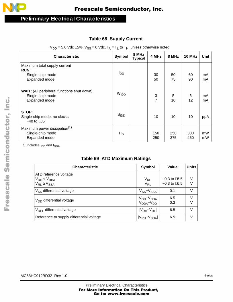
Preliminary Electrical Characteristics
F
ree
sca
le S
em
ico
nd
uc
tor,
I
Freescale Semiconductor, Inc.n
c..
.
Table 68 Supply Current
VDD = 5.0 Vdc ±5%, VSS = 0 Vdc, TA = TL to TH, unless otherwise noted
Characteristic Symbol 8 MHzTypical 4 MHz 8 MHz 10 MHz Unit
Maximum total supply currentRUN:
Single-chip modeExpanded mode
IDD 3050
5075
6090
mAmA
WAIT: (All peripheral functions shut down)Single-chip modeExpanded mode
WIDD 37
510
612
mAmA
STOP:Single-chip mode, no clocks
−40 to +85
SIDD 10 10 10 µµA
Maximum power dissipation(1)
Single-chip modeExpanded mode
PD 150250
250375
300450
mWmW
1. Includes IDD and IDDA.
Table 69 ATD Maximum Ratings
Characteristic Symbol Value Units
ATD reference voltageVRH ≤ VDDAVRL ≥ VSSA
VRHVRL
−0.3 to +6.5−0.3 to +6.5
VV
VSS differential voltage |VSS−VSSA| 0.1 V
VDD differential voltageVDD−VDDAVDDA−VDD
6.50.3
VV
VREF differential voltage |VRH−VRL| 6.5 V
Reference to supply differential voltage |VRH−VDDA| 6.5 V
MC68HC912BD32 Rev 1.0
Preliminary Electrical Characteristics For More Information On This Prod
Go to: www.freescale.com
4-elec
uct,

Preliminary Electrical Characteristics
F
ree
sca
le S
em
ico
nd
uc
tor,
I
Freescale Semiconductor, Inc.n
c..
.
Table 70 ATD DC Electrical Characteristics
VDD = 5.0 Vdc ±5%, VSS = 0 Vdc, TA = TL to TH, ATD Clock = 2 MHz, unless otherwise noted
Characteristic Symbol Min Max Unit
Analog supply voltage VDDA 4.75 5.25 V
Analog supply current, normal operation IDDA 1.0 mA
Reference voltage, low VRL VSSA VDDA/2 V
Reference voltage, high VRH VDDA/2 VDDA V
VREF differential reference voltage(1) VRH−VRL 4.75 5.25 V
Input voltage(2) VINDC VSSA VDDA V
Input current, off channel(3) IOFF 100 nA
Reference supply current IREF 250 µA
Input capacitanceNot SamplingSampling
CINNCINS
1015
pFpF
1. Accuracy is guaranteed at VRH − VRL = 5.0V ±5%.2. To obtain full-scale, full-range results, VSSA ≤ VRL ≤ VINDC ≤ VRH ≤ VDDA.3. Maximum leakage occurs at maximum operating temperature. Current decreases by approximately
one-half for each 10°C decrease from maximum temperature.
MC68HC912BD32 Rev 1.0
5-elecPreliminary Electrical Characteristics For More Information On This Product,
Go to: www.freescale.com

Preliminary Electrical Characteristics
F
ree
sca
le S
em
ico
nd
uc
tor,
I
Freescale Semiconductor, Inc.n
c..
.
Table 71 Analog Converter Characteristics (Operating)
VDD = 5.0 Vdc ±5%, VSS = 0 Vdc, TA = TL to TH, ATD Clock = 2 MHz, unless otherwise noted
Characteristic Symbol Min Typical Max Unit
8-Bit resolution(1) 1 count 20 mV
8-Bit Differential non-linearity(2) DNL −0.5 +0.5 count
8-Bit Integral non-linearity(2) INL −1 +1 count
8- Bit Absolute error(2),(3) AE −1 +1 count
10-Bit Resolution1 1 count 5 mV
10-Bit Differential non-linearity(2) DNL -1 1 count
10-Bit Integral non-linearity(2) INL -2 2 count
10-Bit Absolute error(2),(3) AE -2 2 count
Maximum source impedance RS 20 See note(4) KΩ
1. VRH − VRL ≥ 5.12V; VDDA − VSSA = 5.12V2. At VREF = 5.12V, one 8-bit count = 20 mV, and one 10-bit count = 5mV.3. These values include quantization error which is inherently 1/2 count for any A/D converter.4. Maximum source impedance is application-dependent. Error resulting from pin leakage depends on junction leakage into
the pin and on leakage due to charge-sharing with internal capacitance.Error from junction leakage is a function of external source impedance and input leakage current. Expected error in resultvalue due to junction leakage is expressed in voltage (VERRJ):
VERRJ = RS × IOFF
where IOFF is a function of operating temperature. Charge-sharing effects with internal capacitors are a function of ATDclock speed, the number of channels being scanned, and source impedance. For 8-bit conversions, charge pump leakageis computed as follows:
VERRJ = .25pF × VDDA × RS × ATDCLK/(8 × number of channels)
MC68HC912BD32 Rev 1.0
Preliminary Electrical Characteristics For More Information On This Prod
Go to: www.freescale.com
6-elec
uct,

Preliminary Electrical Characteristics
MC68HC912BD32 Rev 1.0
F
ree
sca
le S
em
ico
nd
uc
tor,
I
Freescale Semiconductor, Inc.n
c..
.
7-elec
Table 72 ATD AC Characteristics (Operating)
VDD = 5.0 Vdc ±5%, VSS = 0 Vdc, TA = TL to TH, ATD Clock = 2 MHz, unless otherwise noted
Characteristic Symbol Min Max Unit
MCU clock frequency (p-clock) fPCLK 2.0 10.0 MHz
ATD operating clock frequency fATDCLK 0.5 2.0 MHz
ATD 8-Bit conversion periodclock cycles(1)
conversion time(2)
nCONV8tCONV8
189
3216
cyclesµs
ATD 10-Bit conversion periodclock cycles1
conversion time2
nCONV10tCONV10
2010
3417
cyclesµs
Stop and ATD power up recovery time(3)
VDDA = 5.0VtSR 10 µs
1. The minimum time assumes a final sample period of 2 ATD clock cycles while the maximum time as-sumes a final sample period of 16ATD clocks.
2. This assumes an ATD clock frequency of 2.0MHz.3. From the time ADPU is asserted until the time an ATD conversion can begin.
Table 73 EEPROM Characteristics
VDD = 5.0 Vdc ±5%, VSS = 0 Vdc, TA = TL to TH, unless otherwise noted
Characteristic Symbol Min Typical Max Unit
Minimum programming clock frequency(1) fPROG 1.0 MHz
Programming time tPROG 10 ms
Clock recovery time, following STOP, to continue programming tCRSTOP tPROG+ 1 ms
Erase time tERASE 10 ms
Write/erase endurance 10,00030,000
(2) cycles
Data retention 10 years
1. RC oscillator must be enabled if programming is desired and fSYS < fPROG.2. If average TH is below 85° C.
Preliminary Electrical Characteristics For More Information On This Product,
Go to: www.freescale.com

Preliminary Electrical Characteristics
F
ree
sca
le S
em
ico
nd
uc
tor,
I
Freescale Semiconductor, Inc.n
c..
.
Table 74 Flash EEPROM Characteristics
VDD = 5.0 Vdc ±5%, VSS = 0 Vdc, TA = TL to TH, unless otherwise noted
Characteristic Symbol Min Typical Max Units
Program/erase supply voltage:Read onlyProgram / erase / verify(1)
VFP VDD−0.511.4
VDD12.0
VDD+0.5
12.6
VV
Program/erase supply currentWord program (VFP = 12V)Erase (VFP = 12V)
IFP 304
mAmA
Number of programming pulses nPP 50 pulses
Programming pulse tPPULSE 20 25 µs
Program to verify time tVPROG 10 µs
Program margin pm 100(2) %
Number of erase pulses nEP 5 pulses
Erase pulse tEPULSE 5 10 ms
Erase to verify time tVERASE 1 ms
Erase margin em 100(2) %
Program/erase endurance 100 cycles
Data retention 10 years
1. Refer to errata for problem description and suggested workaround.2. The number of margin pulses required is the same as the number of pulses used to program or erase.
MC68HC912BD32 Rev 1.0
Preliminary Electrical Characteristics For More Information On This Prod
Go to: www.freescale.com
8-elec
uct,
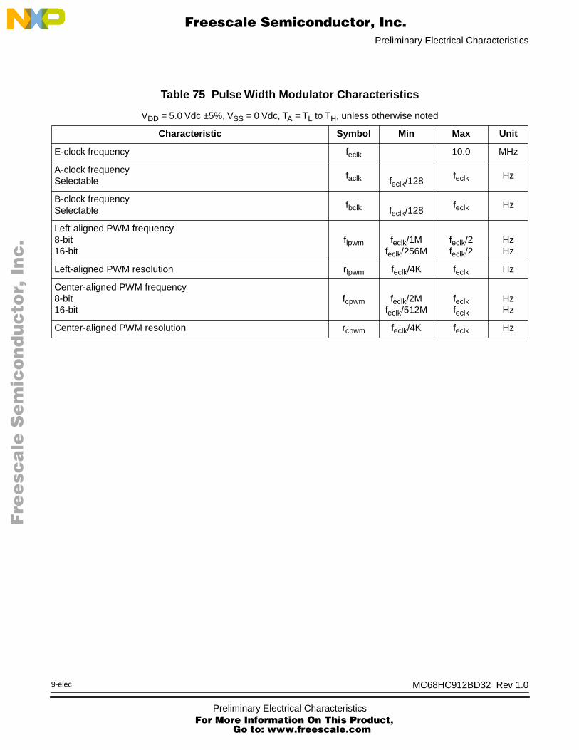
Preliminary Electrical Characteristics
MC68HC912BD32 Rev 1.0
F
ree
sca
le S
em
ico
nd
uc
tor,
I
Freescale Semiconductor, Inc.n
c..
.
9-elec
Table 75 Pulse Width Modulator Characteristics
VDD = 5.0 Vdc ±5%, VSS = 0 Vdc, TA = TL to TH, unless otherwise noted
Characteristic Symbol Min Max Unit
E-clock frequency feclk 10.0 MHz
A-clock frequencySelectable
faclk feclk/128feclk Hz
B-clock frequencySelectable
fbclk feclk/128feclk Hz
Left-aligned PWM frequency8-bit16-bit
flpwm feclk/1Mfeclk/256M
feclk/2feclk/2
HzHz
Left-aligned PWM resolution rlpwm feclk/4K feclk Hz
Center-aligned PWM frequency8-bit16-bit
fcpwm feclk/2Mfeclk/512M
feclkfeclk
HzHz
Center-aligned PWM resolution rcpwm feclk/4K feclk Hz
Preliminary Electrical Characteristics For More Information On This Product,
Go to: www.freescale.com
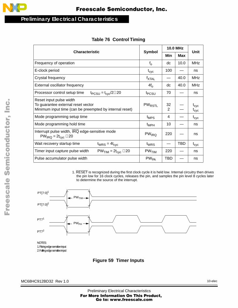
Preliminary Electrical Characteristics
F
ree
sca
le S
em
ico
nd
uc
tor,
I
Freescale Semiconductor, Inc.n
c..
.
1. RESET is recognized during the first clock cycle it is held low. Internal circuitry then drivesthe pin low for 16 clock cycles, releases the pin, and samples the pin level 8 cycles laterto determine the source of the interrupt.
Figure 59 Timer Inputs
Table 76 Control Timing
Characteristic Symbol 10.0 MHz
UnitMin Max
Frequency of operation fo dc 10.0 MHz
E-clock period tcyc 100 — ns
Crystal frequency fXTAL — 40.0 MHz
External oscillator frequency 4fo dc 40.0 MHz
Processor control setup time tPCSU = tcyc/2+ 20 tPCSU 70 — ns
Reset input pulse widthTo guarantee external reset vectorMinimum input time (can be preempted by internal reset)
PWRSTL 322
——
tcyctcyc
Mode programming setup time tMPS 4 — tcyc
Mode programming hold time tMPH 10 — ns
Interrupt pulse width, IRQ edge-sensitive modePWIRQ = 2tcyc + 20
PWIRQ 220 — ns
Wait recovery startup time tWRS = 4tcyc tWRS — TBD tcyc
Timer input capture pulse width PWTIM = 2tcyc + 20 PWTIM 220 — ns
Pulse accumulator pulse width PWPA TBD — ns
PT72
PT71
PT[7:0]2
PT[7:0]1
NOTES:1. Rising edge sensitive input2. Falling edge sensitive input
PWTIM
PWPA
MC68HC912BD32 Rev 1.0
Preliminary Electrical Characteristics For More Information On This Prod
Go to: www.freescale.com
10-elec
uct,

Preliminary Electrical Characteristics
MC68HC912BD32 Rev 1.0
F
ree
sca
le S
em
ico
nd
uc
tor,
I
Freescale Semiconductor, Inc.n
c..
.
11-elec
Figure 60 POR and External Reset Timing Diagram
t PC
SU
INT
ER
NA
L
MO
DA
, MO
DB
EC
LK
EX
TA
L
VD
D
RE
SE
T
4098
t cyc
FREE
FFFE
FFFE
3RD
1ST
2ND
FREE
FFFE
FFFE
FFFE
t MP
H
PWR
ST
L t MP
S
AD
DR
ES
SPI
PEPI
PEPI
PE1S
TEX
EC3R
DPI
PE2N
DPI
PE1S
TPI
PE1S
TEX
EC
NO
TE
: Res
et ti
min
g is
sub
ject
to c
hang
e.
Preliminary Electrical Characteristics For More Information On This Product,
Go to: www.freescale.com

Preliminary Electrical Characteristics
F
ree
sca
le S
em
ico
nd
uc
tor,
I
Freescale Semiconductor, Inc.n
c..
.
Figure 61 STOP Recovery Timing Diagram
PWIR
Q
t ST
OP
DE
LAY
3
IRQ
1
IRQ
or X
IRQ
EC
LK
1ST
AD
DR
ES
S4
SP
-9
FR
EE
FR
EE
VE
CT
OR
FR
EE
FR
EE R
esum
e pr
ogra
m w
ith in
stru
ctio
n w
hich
follo
ws
the
ST
OP
inst
ruct
ion.
INT
ER
NA
L
AD
DR
ES
S5
CLO
CK
S
NO
TES:
1. E
dge
Sens
itive
IRQ
pin
(IRQ
E bit
= 1
)2.
Lev
el se
nsitiv
e IR
Q p
in (IR
QE
bit =
0)
3. t S
TO
PD
ELA
Y =
409
8 t cy
c if D
LY b
it = 1
or 2
t cyc
if DLY
= 0
.4.
XIR
Q w
ith X
bit in
CC
R =
1.
5. IR
Q o
r (XIR
Q w
ith X
bit in
CC
R =
0).
OP
T1S
T
2ND
3RD
1ST
EX
EC
PIP
EP
IPE
EX
EC
SP
-8S
P-6
FE
TC
H
PIP
ES
P-6
SP
-8S
P-9
MC68HC912BD32 Rev 1.0
Preliminary Electrical Characteristics For More Information On This Prod
Go to: www.freescale.com
12-elec
uct,
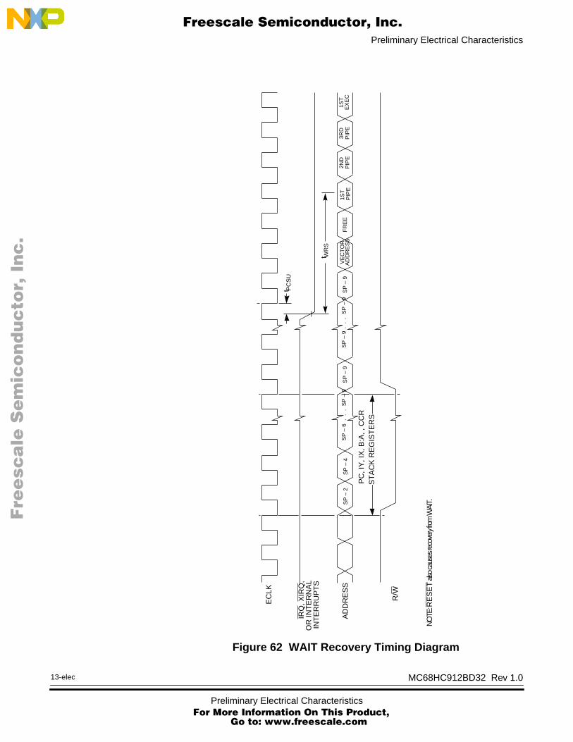
Preliminary Electrical Characteristics
MC68HC912BD32 Rev 1.0
F
ree
sca
le S
em
ico
nd
uc
tor,
I
Freescale Semiconductor, Inc.n
c..
.
13-elec
Figure 62 WAIT Recovery Timing Diagram
t PC
SU
PC
, IY
, IX
, B:A
, , C
CR
ST
AC
K R
EG
IST
ER
S
EC
LK
R/W
AD
DR
ES
S
IRQ
, XIR
Q,
OR
INT
ER
NA
LIN
TE
RR
UP
TS
SP
– 2
SP
– 4
SP
– 6
. .
. S
P –
9S
P –
9S
P –
9 .
. .
SP
– 9
SP
– 9
VE
CT
OR
FR
EE
1ST
2ND
3RD
PIP
E
t WR
S
NO
TE: R
ES
ET
also
caus
es re
cove
ry fro
m W
AIT.
AD
DR
ES
SP
IPE
PIP
E1S
TE
XE
C
Preliminary Electrical Characteristics For More Information On This Product,
Go to: www.freescale.com
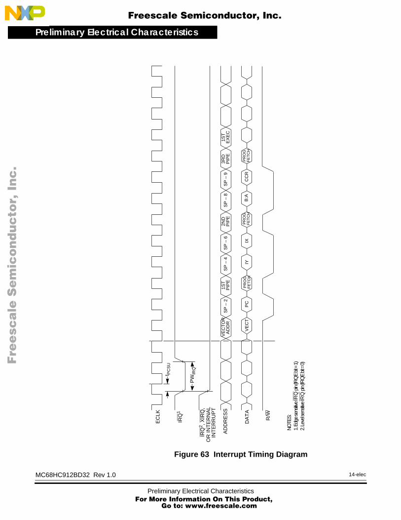
Preliminary Electrical Characteristics
F
ree
sca
le S
em
ico
nd
uc
tor,
I
Freescale Semiconductor, Inc.n
c..
.
Figure 63 Interrupt Timing Diagram
EC
LK
PW
IRQ
1ST
3RD
AD
DR
ES
S
IRQ
1
SP
– 9
t PC
SU
IRQ
2 , X
IRQ
,O
R IN
TE
RN
AL
INT
ER
RU
PT
VE
CT
OR
SP
– 2
1ST
SP
– 4
SP
– 6
2ND
SP
– 8
DA
TA
VE
CT
PC
IYIX
B:A
CC
RP
RO
G
R/W
NO
TES:
1. E
dge
sens
itive
IRQ
pin
(IRQ
E bit
= 1
)2.
Lev
el se
nsitiv
e IR
Q p
in (IR
QE
bit =
0)
FE
TC
H
AD
DR
EX
EC
PIP
EP
IPE
PIP
E
PR
OG
FE
TC
HP
RO
GF
ET
CH
MC68HC912BD32 Rev 1.0
Preliminary Electrical Characteristics For More Information On This Prod
Go to: www.freescale.com
14-elec
uct,
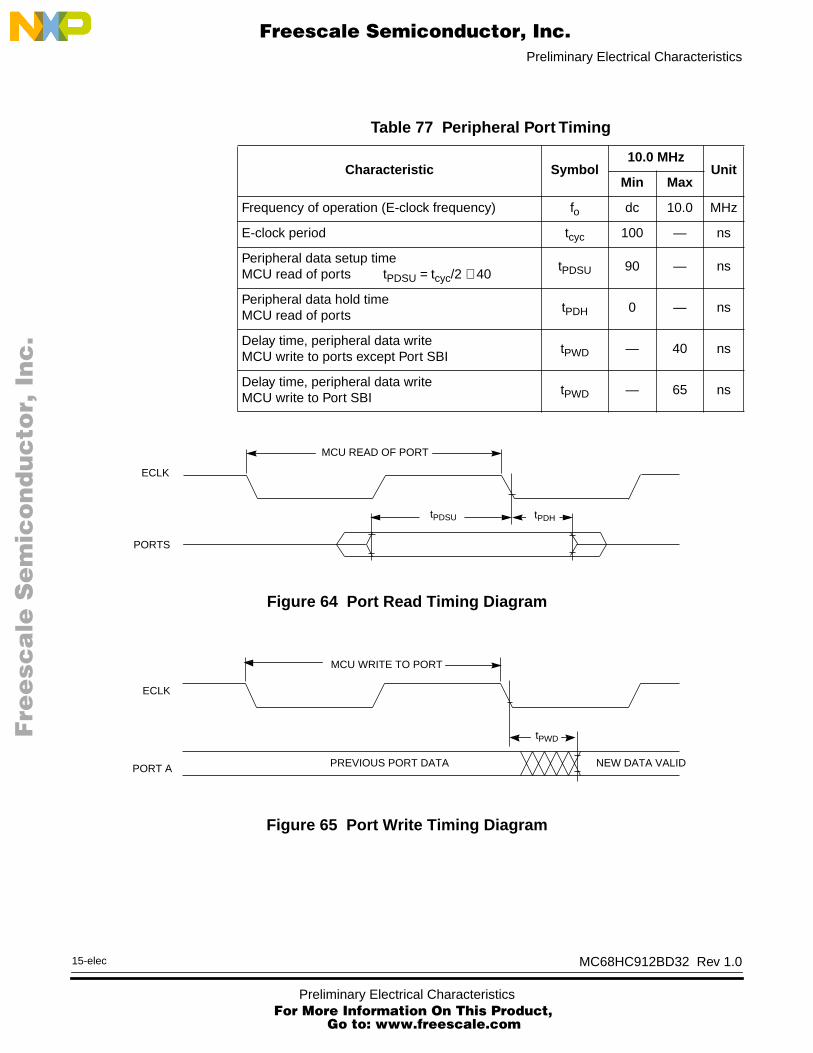
Preliminary Electrical Characteristics
MC68HC912BD32 Rev 1.0
F
ree
sca
le S
em
ico
nd
uc
tor,
I
Freescale Semiconductor, Inc.n
c..
.
15-elec
Figure 64 Port Read Timing Diagram
Figure 65 Port Write Timing Diagram
Table 77 Peripheral Port Timing
Characteristic Symbol 10.0 MHz
UnitMin Max
Frequency of operation (E-clock frequency) fo dc 10.0 MHz
E-clock period tcyc 100 — ns
Peripheral data setup timeMCU read of ports tPDSU = tcyc/2 + 40
tPDSU 90 — ns
Peripheral data hold timeMCU read of ports
tPDH 0 — ns
Delay time, peripheral data writeMCU write to ports except Port SBI
tPWD — 40 ns
Delay time, peripheral data writeMCU write to Port SBI
tPWD — 65 ns
ECLK
MCU READ OF PORT
PORTS
tPDSU tPDH
ECLK
MCU WRITE TO PORT
PREVIOUS PORT DATA NEW DATA VALIDPORT A
tPWD
Preliminary Electrical Characteristics For More Information On This Product,
Go to: www.freescale.com

Preliminary Electrical Characteristics
F
ree
sca
le S
em
ico
nd
uc
tor,
I
Freescale Semiconductor, Inc.n
c..
.
Table 78 Multiplexed Expansion Bus TimingVDD = 5.0 Vdc ± 5%, VSS = 0 Vdc, TA = TL to TH, unless otherwise noted
Num Characteristic (1), (2), (3), (4) Delay Symbol10 MHz
UnitMin Max
Frequency of operation (E-clock frequency) fo dc 10.0 MHz
1 Cycle time tcyc = 1/fo — tcyc 100 — ns
2 Pulse width, E low PWEL = tcyc/2 + delay −2 PWEL 48 — ns
3 Pulse width, E high(5) PWEH = tcyc/2 + delay −2 PWEH 48 — ns
5 Address delay time tAD = tcyc/4 + delay 29 tAD — 54 ns
7 Address valid time to ECLK rise tAV = PWEL − tAD — tAV 0 — ns
8 Multiplexed address hold time tMAH = tcyc/4 + delay −21 tMAH 4 — ns
9 Address Hold to Data Valid — tAHDS 30 —
10 Data Hold to High Z tDHZ = tAD − 20 — tDHZ — 34
11 Read data setup time — tDSR 30 — ns
12 Read data hold time — tDHR 0 — ns
13 Write data delay time — tDDW — 47 ns
14 Write data hold time — tDHW 20 — ns
15 Write data setup time(5) tDSW = PWEH − tDDW — tDSW 1 — ns
16 Read/write delay time tRWD = tcyc/4 + delay 18 tRWD — 43 ns
17 Read/write valid time to E rise tRWV = PWEL − tRWD — tRWV 5 — ns
18 Read/write hold time — tRWH 20 — ns
19 Low strobe(7) delay time tLSD = tcyc/4 + delay 18 tLSD — 43 ns
20 Low strobe(7) valid time to E rise tLSV = PWEL − tLSD — tLSV 5 — ns
21 Low strobe(7) hold time — tLSH 20 — ns
22 Address access time(5) tACCA = tcyc − tAD − tDSR — tACCA — 16 ns
23 Access time from E rise(5) tACCE = PWEH − tDSR — tACCE — 18 ns
24 DBE delay from ECLK rise(5) tDBED = tcyc/4 + delay 6 tDBED — 31 ns
25 DBE valid time tDBE = PWEH − tDBED — tDBE 17 — ns
26 DBE hold time from ECLK fall — tDBEH 0 10 ns
1. All timings are calculated for normal port drives.2. Crystal input is required to be within 45% to 55% duty.3. Reduced drive must be off to meet these timings.4. Unequalled loading of pins will affect relative timing numbers.5. This characteristic is affected by clock stretch.
Add N × tcyc where N = 0, 1, 2, or 3, depending on the number of clock stretches.6. Equation still under evaluation7. Without TAG enabled.
MC68HC912BD32 Rev 1.0
Preliminary Electrical Characteristics For More Information On This Prod
Go to: www.freescale.com
16-elec
uct,
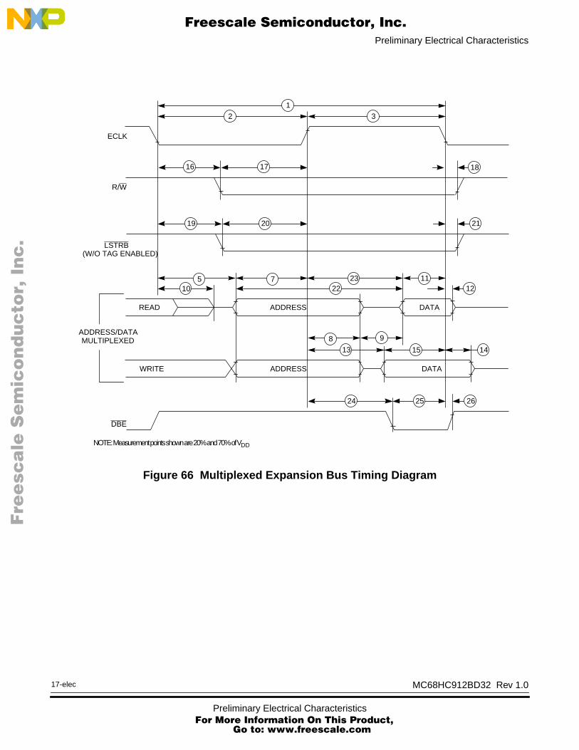
Preliminary Electrical Characteristics
MC68HC912BD32 Rev 1.0
F
ree
sca
le S
em
ico
nd
uc
tor,
I
Freescale Semiconductor, Inc.n
c..
.
17-elec
Figure 66 Multiplexed Expansion Bus Timing Diagram
DBE
24 25
ECLK
R/W
1
2 3
18
1112
14
NOTE: Measurement points shown are 20% and 70% of VDD
13
16 17
READ
WRITE
23
LSTRB
2119 20
(W/O TAG ENABLED)
5 722
8
15
ADDRESS/DATAMULTIPLEXED
ADDRESS
ADDRESS
DATA
DATA
10
9
26
Preliminary Electrical Characteristics For More Information On This Product,
Go to: www.freescale.com
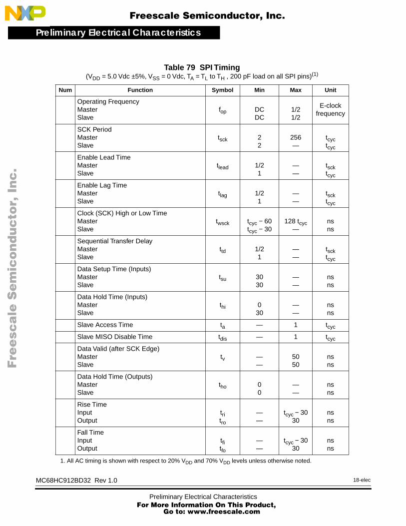
Preliminary Electrical Characteristics
F
ree
sca
le S
em
ico
nd
uc
tor,
I
Freescale Semiconductor, Inc.n
c..
.
Table 79 SPI Timing(VDD = 5.0 Vdc ±5%, VSS = 0 Vdc, TA = TL to TH , 200 pF load on all SPI pins)(1)
Num Function Symbol Min Max Unit
Operating FrequencyMasterSlave
fop DCDC
1/21/2
E-clock frequency
SCK PeriodMasterSlave
tsck 22
256—
tcyctcyc
Enable Lead TimeMasterSlave
tlead 1/21
——
tscktcyc
Enable Lag TimeMasterSlave
tlag 1/21
——
tscktcyc
Clock (SCK) High or Low TimeMasterSlave
twsck tcyc − 60tcyc − 30
128 tcyc—
nsns
Sequential Transfer DelayMasterSlave
ttd 1/21
——
tscktcyc
Data Setup Time (Inputs)MasterSlave
tsu 3030
——
nsns
Data Hold Time (Inputs)MasterSlave
thi 030
——
nsns
Slave Access Time ta — 1 tcyc
Slave MISO Disable Time tdis — 1 tcyc
Data Valid (after SCK Edge)MasterSlave
tv ——
5050
nsns
Data Hold Time (Outputs)MasterSlave
tho 00
——
nsns
Rise TimeInputOutput
tritro
——
tcyc − 3030
nsns
Fall TimeInputOutput
tfitfo
——
tcyc − 3030
nsns
1. All AC timing is shown with respect to 20% VDD and 70% VDD levels unless otherwise noted.
MC68HC912BD32 Rev 1.0
Preliminary Electrical Characteristics For More Information On This Prod
Go to: www.freescale.com
18-elec
uct,

Preliminary Electrical Characteristics
MC68HC912BD32 Rev 1.0
F
ree
sca
le S
em
ico
nd
uc
tor,
I
Freescale Semiconductor, Inc.n
c..
.
19-elec
A) SPI Master Timing (CPHA = 0)
B) SPI Master Timing (CPHA = 1)
Figure 67 SPI Timing Diagram (1 of 2)
SCK
(OUTPUT)
SCK
(OUTPUT)
MISO(INPUT)
MOSI(OUTPUT)
SS1
(OUTPUT)
1
10
6 7
MSB IN2
BIT 6 . . . 1
LSB IN
MSB OUT2 LSB OUT
BIT 6 . . . 1
11
4
4
2
10
(CPOL = 0)
(CPOL = 1)
5
312
13
1. SS output mode (DDS7 = 1, SSOE = 1).2. LSBF = 0. For LSBF = 1, bit order is LSB, bit 1, ..., bit 6, MSB.
SCK
(OUTPUT)
SCK
(OUTPUT)
MISO(INPUT)
MOSI(OUTPUT)
1
6 7
MSB IN2
BIT 6 . . . 1
LSB IN
MASTER MSB OUT2 MASTER LSB OUT
BIT 6 . . . 1
44
10
12 13
11
PORT DATA
(CPOL = 0)
(CPOL = 1)
PORT DATA
SS1
(OUTPUT)5
2 13 12 3
1. SS output mode (DDS7 = 1, SSOE = 1).2. LSBF = 0. For LSBF = 1, bit order is LSB, bit 1, ..., bit 6, MSB.
Preliminary Electrical Characteristics For More Information On This Product,
Go to: www.freescale.com

Preliminary Electrical Characteristics
F
ree
sca
le S
em
ico
nd
uc
tor,
I
Freescale Semiconductor, Inc.n
c..
.
A) SPI Slave Timing (CPHA = 0)
B) SPI Slave Timing (CPHA = 1)
Figure 68 SPI Timing Diagram (2 of 2)
SCK
(INPUT)
SCK
(INPUT)
MOSI(INPUT)
MISO(OUTPUT)
SS(INPUT)
1
10
6 7
MSB IN
BIT 6 . . . 1
LSB IN
MSB OUT SLAVE LSB OUT
BIT 6 . . . 1
11
442
8
(CPOL = 0)
(CPOL = 1)
5
3
13
NOTE: Not defined but normally MSB of character just received.
SLAVE
13
12
11
SEE
12
NOTE
9
SCK
(INPUT)
SCK
(INPUT)
MOSI(INPUT)
MISO(OUTPUT)
1
6 7
MSB IN
BIT 6 . . . 1
LSB IN
MSB OUT SLAVE LSB OUT
BIT 6 . . . 1
44
10
12 13
11
SEE
(CPOL = 0)
(CPOL = 1)
SS(INPUT)
5
2 13 12
3
NOTE: Not defined but normally LSB of character just received.
SLAVE NOTE
8
9
MC68HC912BD32 Rev 1.0
Preliminary Electrical Characteristics For More Information On This Prod
Go to: www.freescale.com
20-elec
uct,
F
ree
sca
le S
em
ico
nd
uc
tor,
IFreescale Semiconductor, Inc.
nc
...
Literature UpdatesLiterature Updates
This document contains the latest data available at publication time. For updates, contact one of the centers listed below:
Literature Distribution Centers
Order literature by mail or phone.
USA/Europe Motorola Literature DistributionP.O. Box 5405Denver, Colorado, 80217Phone 1-303-675-2140
Japan Motorola Japan Ltd.Tatsumi-SPD-JLDCToshikatsu Otsuki6F Seibu-Butsuryu Center3-14-2 Tatsumi Koto-KuTokyo 135, JapanPhone 03-3521-8315
Hong Kong Motorola Semiconductors H.K. Ltd.8B Tai Ping Industrial Park51 Ting Kok RoadTai Po, N.T., Hong KongPhone 852-26629298
MC68HC912BD32 Rev 1.0
Literature Updates For More Information On This Product,
Go to: www.freescale.com

Literature Updates
F
ree
sca
le S
em
ico
nd
uc
tor,
I
Freescale Semiconductor, Inc.n
c..
.
Customer Focus Center
1-800-521-6274
Microcontroller Division’s Web Site
Directly access the Microcontroller Division’s web site with the following URL:
http://mcu.motsps.com/
MC68HC912BD32 Rev 1.0
Literature Updates For More Information On This Prod
Go to: www.freescale.com
uct,
F
ree
sca
le S
em
ico
nd
uc
tor,
IFreescale Semiconductor, Inc.
nc
...
GlossaryGlossary
A — See “accumulators (A and B or D).”
accumulators (A and B or D) — Two 8-bit (A and B) or one 16-bit (D) general-purpose registers in the CPU. The CPU uses the accumulators to hold operands and results of arithmetic and logic operations.
acquisition mode — A mode of PLL operation with large loop bandwidth. Also see ’tracking mode’.
address bus — The set of wires that the CPU uses to read and write memory locations.
addressing mode — The way that the CPU determines the operand address for an instruction. The M68HC12 CPU has 15 addressing modes.
ALU — See “arithmetic logic unit (ALU).”
analogue-to-digital converter (ATD) — The ATD module is an 8-channel, multiplexed-input successive-approximation analog-to-digital converter.
arithmetic logic unit (ALU) — The portion of the CPU that contains the logic circuitry to perform arithmetic, logic, and manipulation operations on operands.
asynchronous — Refers to logic circuits and operations that are not synchronized by a common reference signal.
ATD — See “analogue-to-digital converter”.
B — See “accumulators (A and B or D).”
baud rate — The total number of bits transmitted per unit of time.
BCD — See “binary-coded decimal (BCD).”
binary — Relating to the base 2 number system.
binary number system — The base 2 number system, having two digits, 0 and 1. Binary arithmetic is convenient in digital circuit design because digital circuits have two permissible voltage levels, low and high. The binary digits 0 and 1 can be interpreted to correspond to the two digital voltage levels.
MC68HC912BD32 Rev 1.0
Glossary For More Information On This Product,
Go to: www.freescale.com

Glossary
F
ree
sca
le S
em
ico
nd
uc
tor,
I
Freescale Semiconductor, Inc.n
c..
.
binary-coded decimal (BCD) — A notation that uses 4-bit binary numbers to represent the 10 decimal digits and that retains the same positional structure of a decimal number. For example,
234 (decimal) = 0010 0011 0100 (BCD)
bit — A binary digit. A bit has a value of either logic 0 or logic 1.
branch instruction — An instruction that causes the CPU to continue processing at a memory location other than the next sequential address.
break module — The break module allows software to halt program execution at a programmable point in order to enter a background routine.
breakpoint — A number written into the break address registers of the break module. When a number appears on the internal address bus that is the same as the number in the break address registers, the CPU executes the software interrupt instruction (SWI).
break interrupt — A software interrupt caused by the appearance on the internal address bus of the same value that is written in the break address registers.
bus — A set of wires that transfers logic signals.
bus clock — See "CPU clock".
byte — A set of eight bits.
CAN — See "Motorola scalable CAN."
CCR — See “condition code register.”
central processor unit (CPU) — The primary functioning unit of any computer system. The CPU controls the execution of instructions.
CGM — See “clock generator module (CGM).”
clear — To change a bit from logic 1 to logic 0; the opposite of set.
clock — A square wave signal used to synchronize events in a computer.
clock generator module (CGM) — The CGM module generates a base clock signal from which the system clocks are derived. The CGM may include a crystal oscillator circuit and/or phase-locked loop (PLL) circuit.
comparator — A device that compares the magnitude of two inputs. A digital comparator defines the equality or relative differences between two binary numbers.
MC68HC912BD32 Rev 1.0
Glossary For More Information On This Product,
Go to: www.freescale.com

Glossary
F
ree
sca
le S
em
ico
nd
uc
tor,
I
Freescale Semiconductor, Inc.n
c..
.
computer operating properly module (COP) — A counter module that resets the MCU if allowed to overflow.
condition code register (CCR) — An 8-bit register in the CPU that contains the interrupt mask bit and five bits that indicate the results of the instruction just executed.
control bit — One bit of a register manipulated by software to control the operation of the module.
control unit — One of two major units of the CPU. The control unit contains logic functions that synchronize the machine and direct various operations. The control unit decodes instructions and generates the internal control signals that perform the requested operations. The outputs of the control unit drive the execution unit, which contains the arithmetic logic unit (ALU), CPU registers, and bus interface.
COP — See "computer operating properly module (COP)."
CPU — See “central processor unit (CPU).”
CPU12 — The CPU of the MC68HC12 Family.
CPU clock — Bus clock select bits BCSP and BCSS in the clock select register (CLKSEL) determine which clock drives SYSCLK for the main system, including the CPU and buses. When EXTALi drives the SYSCLK, the CPU or bus clock frequency (fo) is equal to the EXTALi frequency divided by 2.
CPU cycles — A CPU cycle is one period of the internal bus clock, normally derived by dividing a crystal oscillator source by two or more so the high and low times will be equal. The length of time required to execute an instruction is measured in CPU clock cycles.
CPU registers — Memory locations that are wired directly into the CPU logic instead of being part of the addressable memory map. The CPU always has direct access to the information in these registers. The CPU registers in an M68HC12 are:
• A (8-bit accumulator)
• B (8-bit accumulator)
– D (16-bit accumulator formed by concatenation of accumulators A and B)
• IX (16-bit index register)
• IY (16-bit index register)
• SP (16-bit stack pointer)
• PC (16-bit program counter)
• CCR (8-bit condition code register)
MC68HC912BD32 Rev 1.0
Glossary For More Information On This Product,
Go to: www.freescale.com

Glossary
F
ree
sca
le S
em
ico
nd
uc
tor,
I
Freescale Semiconductor, Inc.n
c..
.
cycle time — The period of the operating frequency: tCYC = 1/fOP.
D — See “accumulators (A and B or D).”
decimal number system — Base 10 numbering system that uses the digits zero through nine.
duty cycle — A ratio of the amount of time the signal is on versus the time it is off. Duty cycle is usually represented by a percentage.
ECT — See “enhanced capture timer.”
EEPROM — Electrically erasable, programmable, read-only memory. A nonvolatile type of memory that can be electrically erased and reprogrammed.
EPROM — Erasable, programmable, read-only memory. A nonvolatile type of memory that can be erased by exposure to an ultraviolet light source and then reprogrammed.
enhanced capture timer (ECT) — The HC12 Enhanced Capture Timer module has the features of the HC12 Standard Timer module enhanced by additional features in order to enlarge the field of applications.
exception — An event such as an interrupt or a reset that stops the sequential execution of the instructions in the main program.
fetch — To copy data from a memory location into the accumulator.
firmware — Instructions and data programmed into nonvolatile memory.
flash EEPROM — Electrically erasable, programmable, read-only memory. A nonvolatile type of memory that can be electrically erased and reprogrammed. Does not support byte or word erase.
free-running counter — A device that counts from zero to a predetermined number, then rolls over to zero and begins counting again.
full-duplex transmission — Communication on a channel in which data can be sent and received simultaneously.
hexadecimal — Base 16 numbering system that uses the digits 0 through 9 and the letters A through F.
high byte — The most significant eight bits of a word.
illegal address — An address not within the memory map
illegal opcode — A nonexistent opcode.
MC68HC912BD32 Rev 1.0
Glossary For More Information On This Product,
Go to: www.freescale.com

Glossary
F
ree
sca
le S
em
ico
nd
uc
tor,
I
Freescale Semiconductor, Inc.n
c..
.
index registers (IX and IY) — Two 16-bit registers in the CPU. In the indexed addressing modes, the CPU uses the contents of IX or IY to determine the effective address of the operand. IX and IY can also serve as a temporary data storage locations.
input/output (I/O) — Input/output interfaces between a computer system and the external world. A CPU reads an input to sense the level of an external signal and writes to an output to change the level on an external signal.
instructions — Operations that a CPU can perform. Instructions are expressed by programmers as assembly language mnemonics. A CPU interprets an opcode and its associated operand(s) and instruction.
interrupt — A temporary break in the sequential execution of a program to respond to signals from peripheral devices by executing a subroutine.
interrupt request — A signal from a peripheral to the CPU intended to cause the CPU to execute a subroutine.
I/O — See “input/output (I/0).”
jitter — Short-term signal instability.
latch — A circuit that retains the voltage level (logic 1 or logic 0) written to it for as long as power is applied to the circuit.
latency — The time lag between instruction completion and data movement.
least significant bit (LSB) — The rightmost digit of a binary number.
logic 1 — A voltage level approximately equal to the input power voltage (VDD).
logic 0 — A voltage level approximately equal to the ground voltage (VSS).
low byte — The least significant eight bits of a word.
M68HC12 — A Motorola family of 16-bit MCUs.
mark/space — The logic 1/logic 0 convention used in formatting data in serial communication.
mask — 1. A logic circuit that forces a bit or group of bits to a desired state. 2. A photomask used in integrated circuit fabrication to transfer an image onto silicon.
MCU — Microcontroller unit. See “microcontroller.”
MC68HC912BD32 Rev 1.0
Glossary For More Information On This Product,
Go to: www.freescale.com

Glossary
F
ree
sca
le S
em
ico
nd
uc
tor,
I
Freescale Semiconductor, Inc.n
c..
.
memory location — Each M68HC12 memory location holds one byte of data and has a unique address. To store information in a memory location, the CPU places the address of the location on the address bus, the data information on the data bus, and asserts the write signal. To read information from a memory location, the CPU places the address of the location on the address bus and asserts the read signal. In response to the read signal, the selected memory location places its data onto the data bus.
memory map — A pictorial representation of all memory locations in a computer system.
MI-Bus — See "Motorola interconnect bus".
microcontroller — Microcontroller unit (MCU). A complete computer system, including a CPU, memory, a clock oscillator, and input/output (I/O) on a single integrated circuit.
modulo counter — A counter that can be programmed to count to any number from zero to its maximum possible modulus.
most significant bit (MSB) — The leftmost digit of a binary number.
Motorola interconnect bus (MI-Bus) — The Motorola Interconnect Bus (MI Bus) is a serial communications protocol which supports distributed real-time control efficiently and with a high degree of noise immunity.
Motorola scalable CAN (msCAN) — The Motorola scalable controller area network is a serial communications protocol that efficiently supports distributed real-time control with a very high level of data integrity.
msCAN — See "Motorola scalable CAN".
MSI — See "multiple serial interface".
multiple serial interface — A module consisting of multiple independent serial I/O sub-systems, e.g. two SCI and one SPI.
multiplexer — A device that can select one of a number of inputs and pass the logic level of that input on to the output.
nibble — A set of four bits (half of a byte).
object code — The output from an assembler or compiler that is itself executable machine code, or is suitable for processing to produce executable machine code.
opcode — A binary code that instructs the CPU to perform an operation.
open-drain — An output that has no pullup transistor. An external pullup device can be connected to the power supply to provide the logic 1 output voltage.
MC68HC912BD32 Rev 1.0
Glossary For More Information On This Product,
Go to: www.freescale.com

Glossary
F
ree
sca
le S
em
ico
nd
uc
tor,
I
Freescale Semiconductor, Inc.n
c..
.
operand — Data on which an operation is performed. Usually a statement consists of an operator and an operand. For example, the operator may be an add instruction, and the operand may be the quantity to be added.
oscillator — A circuit that produces a constant frequency square wave that is used by the computer as a timing and sequencing reference.
OTPROM — One-time programmable read-only memory. A nonvolatile type of memory that cannot be reprogrammed.
overflow — A quantity that is too large to be contained in one byte or one word.
page zero — The first 256 bytes of memory (addresses $0000–$00FF).
parity — An error-checking scheme that counts the number of logic 1s in each byte transmitted. In a system that uses odd parity, every byte is expected to have an odd number of logic 1s. In an even parity system, every byte should have an even number of logic 1s. In the transmitter, a parity generator appends an extra bit to each byte to make the number of logic 1s odd for odd parity or even for even parity. A parity checker in the receiver counts the number of logic 1s in each byte. The parity checker generates an error signal if it finds a byte with an incorrect number of logic 1s.
PC — See “program counter (PC).”
peripheral — A circuit not under direct CPU control.
phase-locked loop (PLL) — A clock generator circuit in which a voltage controlled oscillator produces an oscillation which is synchronized to a reference signal.
PLL — See "phase-locked loop (PLL)."
pointer — Pointer register. An index register is sometimes called a pointer register because its contents are used in the calculation of the address of an operand, and therefore points to the operand.
polarity — The two opposite logic levels, logic 1 and logic 0, which correspond to two different voltage levels, VDD and VSS.
polling — Periodically reading a status bit to monitor the condition of a peripheral device.
port — A set of wires for communicating with off-chip devices.
prescaler — A circuit that generates an output signal related to the input signal by a fractional scale factor such as 1/2, 1/8, 1/10 etc.
program — A set of computer instructions that cause a computer to perform a desired operation or operations.
MC68HC912BD32 Rev 1.0
Glossary For More Information On This Product,
Go to: www.freescale.com

Glossary
F
ree
sca
le S
em
ico
nd
uc
tor,
I
Freescale Semiconductor, Inc.n
c..
.
program counter (PC) — A 16-bit register in the CPU. The PC register holds the address of the next instruction or operand that the CPU will use.
pull — An instruction that copies into the accumulator the contents of a stack RAM location. The stack RAM address is in the stack pointer.
pullup — A transistor in the output of a logic gate that connects the output to the logic 1 voltage of the power supply.
pulse-width — The amount of time a signal is on as opposed to being in its off state.
pulse-width modulation (PWM) — Controlled variation (modulation) of the pulse width of a signal with a constant frequency.
push — An instruction that copies the contents of the accumulator to the stack RAM. The stack RAM address is in the stack pointer.
PWM period — The time required for one complete cycle of a PWM waveform.
RAM — Random access memory. All RAM locations can be read or written by the CPU. The contents of a RAM memory location remain valid until the CPU writes a different value or until power is turned off.
RC circuit — A circuit consisting of capacitors and resistors having a defined time constant.
read — To copy the contents of a memory location to the accumulator.
register — A circuit that stores a group of bits.
reserved memory location — A memory location that is used only in special factory test modes. Writing to a reserved location has no effect. Reading a reserved location returns an unpredictable value.
reset — To force a device to a known condition.
ROM — Read-only memory. A type of memory that can be read but cannot be changed (written). The contents of ROM must be specified before manufacturing the MCU.
SCI — See "serial communication interface module (SCI)."
serial — Pertaining to sequential transmission over a single line.
serial communications interface module (SCI) — A module that supports asynchronous communication.
serial peripheral interface module (SPI) — A module that supports synchronous communication.
set — To change a bit from logic 0 to logic 1; opposite of clear.
MC68HC912BD32 Rev 1.0
Glossary For More Information On This Product,
Go to: www.freescale.com

Glossary
F
ree
sca
le S
em
ico
nd
uc
tor,
I
Freescale Semiconductor, Inc.n
c..
.
shift register — A chain of circuits that can retain the logic levels (logic 1 or logic 0) written to them and that can shift the logic levels to the right or left through adjacent circuits in the chain.
signed — A binary number notation that accommodates both positive and negative numbers. The most significant bit is used to indicate whether the number is positive or negative, normally logic 0 for positive and logic 1 for negative. The other seven bits indicate the magnitude of the number.
software — Instructions and data that control the operation of a microcontroller.
software interrupt (SWI) — An instruction that causes an interrupt and its associated vector fetch.
SPI — See "serial peripheral interface module (SPI)."
stack — A portion of RAM reserved for storage of CPU register contents and subroutine return addresses.
stack pointer (SP) — A 16-bit register in the CPU containing the address of the next available storage location on the stack.
start bit — A bit that signals the beginning of an asynchronous serial transmission.
status bit — A register bit that indicates the condition of a device.
stop bit — A bit that signals the end of an asynchronous serial transmission.
subroutine — A sequence of instructions to be used more than once in the course of a program. The last instruction in a subroutine is a return from subroutine (RTS) instruction. At each place in the main program where the subroutine instructions are needed, a jump or branch to subroutine (JSR or BSR) instruction is used to call the subroutine. The CPU leaves the flow of the main program to execute the instructions in the subroutine. When the RTS instruction is executed, the CPU returns to the main program where it left off.
synchronous — Refers to logic circuits and operations that are synchronized by a common reference signal.
timer — A module used to relate events in a system to a point in time.
toggle — To change the state of an output from a logic 0 to a logic 1 or from a logic 1 to a logic 0.
tracking mode — A mode of PLL operation with narrow loop bandwidth. Also see ‘acquisition mode.’
MC68HC912BD32 Rev 1.0
Glossary For More Information On This Product,
Go to: www.freescale.com
Glossary
F
ree
sca
le S
em
ico
nd
uc
tor,
I
Freescale Semiconductor, Inc.n
c..
.
two’s complement — A means of performing binary subtraction using addition techniques. The most significant bit of a two’s complement number indicates the sign of the number (1 indicates negative). The two’s complement negative of a number is obtained by inverting each bit in the number and then adding 1 to the result.
unbuffered — Utilizes only one register for data; new data overwrites current data.
unimplemented memory location — A memory location that is not used. Writing to an unimplemented location has no effect. Reading an unimplemented location returns an unpredictable value.
variable — A value that changes during the course of program execution.
VCO — See "voltage-controlled oscillator."
vector — A memory location that contains the address of the beginning of a subroutine written to service an interrupt or reset.
voltage-controlled oscillator (VCO) — A circuit that produces an oscillating output signal of a frequency that is controlled by a dc voltage applied to a control input.
waveform — A graphical representation in which the amplitude of a wave is plotted against time.
wired-OR — Connection of circuit outputs so that if any output is high, the connection point is high.
word — A set of two bytes (16 bits).
write — The transfer of a byte of data from the CPU to a memory location.
MC68HC912BD32 Rev 1.0
Glossary For More Information On This Product,
Go to: www.freescale.com

2
1
3
4
5
6
7
8
9
10
11
12
13
14
15
Fre
esc
ale
Se
mic
on
du
cto
r, I
Freescale Semiconductor, Inc.
For More Information On This Product, Go to: www.freescale.com
nc
...

2
1
3
4
5
6
7
8
9
0
1
2
3
4
5
MC68HC08AZ60/D
Fre
esc
ale
Se
mic
on
du
cto
r, I
Freescale Semiconductor, Inc.
For More Information On This Product, Go to: www.freescale.com
nc
...
RXZB30
hibbertleft
RXZB30
disclaimer
RXZB30
disclaimer
RXZB30
rohstext
RXZB30
logo


![MSI MS-6633 - REV 1.0[1]](https://static.fdocuments.us/doc/165x107/55364c1655034650678b49a1/msi-ms-6633-rev-101.jpg)
