MC68020 MC68EC020 - NXP Semiconductors | … Operation 5.1 Bus Transfer Signals..... 5-1 5.1.1Bus...
306
© MOTOROLA INC., 1992 MC68020 MC68EC020 MICROPROCESSORS USER’S MANUAL First Edition Motorola reserves the right to make changes without further notice to any products herein to improve reliability, function or design. Motorola does not assume any liability arising out of the application or use of any product or circuit described herein; neither does it convey any license under its patent rights nor the rights of others. Motorola products are not designed, intended, or authorized for use as components in systems intended for surgical implant into the body, or other applications intended to support or sustain life, or for any other application in which the failure of the Motorola product could create a situation where personal injury or death may occur. Should Buyer purchase or use Motorola products for any such unintended or unauthorized application, Buyer shall indemnify and hold Motorola and its officers, employees, subsidiaries, affiliates, and distributors harmless against all claims, costs, damages, and expenses, and reasonable attorney fees arising out of, directly or indirectly, any claim of personal injury or death associated with such unintended or unauthorized use, even if such claim alleges that Motorola was negligent regarding the design or manufacture of the part. Motorola and the are registered trademarks of Motorola, Inc. Motorola, Inc. is an Equal Opportunity/Affirmative Action Employer. Freescale Semiconductor, I Freescale Semiconductor, Inc. For More Information On This Product, Go to: www.freescale.com nc...
Transcript of MC68020 MC68EC020 - NXP Semiconductors | … Operation 5.1 Bus Transfer Signals..... 5-1 5.1.1Bus...

© MOTOROLA INC., 1992
MC68020MC68EC020
MICROPROCESSORSUSER’S MANUAL
First Edition
Motorola reserves the right to make changes without further notice to any products herein to improve reliability, function or design. Motorola does not assume any liability arising out of the application or use of any product or circuit described herein; neither does it convey any license under its patent rights nor the rights of others. Motorola products are not designed, intended, or authorized for use as components in systems intended for surgical implant into the body, or other applications intended to support or sustain life, or for any other application in which the failure of the Motorola product could create a situation where personal injury or death may occur. Should Buyer purchase or use Motorola products for any such unintended or unauthorized application, Buyer shall indemnify and hold Motorola and its officers, employees, subsidiaries, affiliates, and distributors harmless against all claims, costs, damages, and expenses, and reasonable attorney fees arising out of, directly or indirectly, any claim of personal injury or death associated with such unintended or unauthorized use, even if such claim alleges that Motorola was negligent regarding the design or manufacture of the part. Motorola and the are registered trademarks of Motorola, Inc. Motorola, Inc. is an Equal Opportunity/Affirmative Action Employer.
Fre
esc
ale
Se
mic
on
du
cto
r, I
Freescale Semiconductor, Inc.
For More Information On This Product, Go to: www.freescale.com
nc
...

MOTOROLA M68020 USER’S MANUAL iii
PREFACEThe M68020 User’s Manual describes the capabilities, operation, and programming of theMC68020 32-bit, second-generation, enhanced microprocessor and the MC68EC020 32-bit, second-generation, enhanced embedded microprocessor.
Throughout this manual, “MC68020/EC020” is used when information applies to both theMC68020 and the MC68EC020. “MC68020” and “MC68EC020” are used wheninformation applies only to the MC68020 or MC68EC020, respectively.
For detailed information on the MC68020 and MC68EC020 instruction set, refer toM68000PM/AD, M68000 Family Programmer’s Reference Manual.
This manual consists of the following sections:
Section 1 IntroductionSection 2 Processing StatesSection 3 Signal DescriptionSection 4 On-Chip Cache MemorySection 5 Bus OperationSection 6 Exception ProcessingSection 7 Coprocessor Interface DescriptionSection 8 Instruction Execution TimingSection 9 Applications InformationSection 10 Electrical CharacteristicsSection 11 Ordering Information and Mechanical DataAppendix A Interfacing an MC68EC020 to a DMA Device That Supports a Three-Wire
Bus Arbitration Protocol
NOTE
In this manual, assert and negate are used to specify forcing asignal to a particular state. In particular, assertion and assertrefer to a signal that is active or true; negation and negateindicate a signal that is inactive or false. These terms are usedindependently of the voltage level (high or low) that theyrepresent.
Fre
esc
ale
Se
mic
on
du
cto
r, I
Freescale Semiconductor, Inc.
For More Information On This Product, Go to: www.freescale.com
nc
...

9/29/95 SECTION 1: OVERVIEW UM Rev 1
MOTOROLA M68020 USER’S MANUAL vii
TABLE OF CONTENTSParagraph Page
Number Title Number
Section 1Introduction
1.1 Features .................................................................................................. 1-21.2 Programming Model ................................................................................ 1-41.3 Data Types and Addressing Modes Overview ........................................ 1-81.4 Instruction Set Overview ......................................................................... 1-101.5 Virtual Memory and Virtual Machine Concepts ....................................... 1-101.5.1 Virtual Memory .................................................................................... 1-101.5.2 Virtual Machine .................................................................................... 1-121.6 Pipelined Architecture ............................................................................. 1-121.7 Cache Memory ........................................................................................ 1-13
Section 2Processing States
2.1 Privilege Levels ....................................................................................... 2-22.1.1 Supervisor Privilege Level ................................................................... 2-22.1.2 User Privilege Level ............................................................................. 2-32.1.3 Changing Privilege Level ..................................................................... 2-32.2 Address Space Types ............................................................................. 2-42.3 Exception Processing.............................................................................. 2-52.3.1 Exception Vectors ................................................................................ 2-52.3.2 Exception Stack Frame ....................................................................... 2-6
Section 3Signal Description
3.1 Signal Index ............................................................................................ 3-23.2 Function Code Signals (FC2–FC0) ......................................................... 3-23.3 Address Bus (A31–A0, MC68020)(A23–A0, MC68EC020) .................... 3-23.4 Data Bus (D31–D0) ................................................................................. 3-23.5 Transfer Size Signals (SIZ1, SIZ0) ......................................................... 3-23.6 Asynchronous Bus Control Signals ......................................................... 3-43.7 Interrupt Control Signals.......................................................................... 3-53.8 Bus Arbitration Control Signals ............................................................... 3-63.9 Bus Exception Control Signals ................................................................ 3-63.10 Emulator Support Signal ......................................................................... 3-73.11 Clock (CLK) ............................................................................................. 3-7
Fre
esc
ale
Se
mic
on
du
cto
r, I
Freescale Semiconductor, Inc.
For More Information On This Product, Go to: www.freescale.com
nc
...

9/29/95 SECTION 1: OVERVIEW UM Rev.1.0
viii M68020 USER’S MANUAL MOTOROLA
TABLE OF CONTENTS (Continued)Paragraph Page
Number Title Number
3.12 Power Supply Connections ..................................................................... 3-73.13 Signal Summary...................................................................................... 3-8
Section 4On-Chip Cache Memory
4.1 On-Chip Cache Organization and Operation .......................................... 4-14.2 Cache Reset ........................................................................................... 4-34.3 Cache Control ......................................................................................... 4-34.3.1 Cache Control Register (CACR) ......................................................... 4-34.3.2 Cache Address Register (CAAR) ........................................................ 4-4
Section 5Bus Operation
5.1 Bus Transfer Signals............................................................................... 5-15.1.1 Bus Control Signals ............................................................................. 5-25.1.2 Address Bus ........................................................................................ 5-35.1.3 Address Strobe .................................................................................... 5-35.1.4 Data Bus.............................................................................................. 5-35.1.5 Data Strobe ......................................................................................... 5-45.1.6 Data Buffer Enable .............................................................................. 5-45.1.7 Bus Cycle Termination Signals............................................................ 5-45.2 Data Transfer Mechanism....................................................................... 5-55.2.1 Dynamic Bus Sizing ............................................................................ 5-55.2.2 Misaligned Operands........................................................................... 5-145.2.3 Effects of Dynamic Bus Sizing and Operand Misalignment ................ 5-205.2.4 Address, Size, and Data Bus Relationships ........................................ 5-215.2.5 Cache Interactions .............................................................................. 5-225.2.6 Bus Operation ..................................................................................... 5-245.2.7 Synchronous Operation with DSACK1/DSACK0 ............................... 5-245.3 Data Transfer Cycles .............................................................................. 5-255.3.1 Read Cycle .......................................................................................... 5-265.3.2 Write Cycle .......................................................................................... 5-335.3.3 Read-Modify-Write Cycle..................................................................... 5-395.4 CPU Space Cycles ................................................................................. 5-445.4.1 Interrupt Acknowledge Bus Cycles ...................................................... 5-455.4.1.1 Interrupt Acknowledge Cycle—Terminated Normally ...................... 5-455.4.1.2 Autovector Interrupt Acknowledge Cycle ......................................... 5-485.4.1.3 Spurious Interrupt Cycle .................................................................. 5-485.4.2 Breakpoint Acknowledge Cycle ........................................................... 5-505.4.3 Coprocessor Communication Cycles .................................................. 5-535.5 Bus Exception Control Cycles................................................................. 5-535.5.1 Bus Errors ........................................................................................... 5-55
Fre
esc
ale
Se
mic
on
du
cto
r, I
Freescale Semiconductor, Inc.
For More Information On This Product, Go to: www.freescale.com
nc
...

9/29/95 SECTION 1: OVERVIEW UM Rev 1
MOTOROLA M68020 USER’S MANUAL ix
TABLE OF CONTENTS (Continued)Paragraph Page
Number Title Number
5.5.2 Retry Operation ................................................................................... 5-565.5.3 Halt Operation...................................................................................... 5-605.5.4 Double Bus Fault ................................................................................. 5-605.6 Bus Synchronization................................................................................ 5-625.7 Bus Arbitration ......................................................................................... 5-625.7.1 MC68020 Bus Arbitration .................................................................... 5-635.7.1.1 Bus Request (MC68020) ................................................................. 5-665.7.1.2 Bus Grant (MC68020) ...................................................................... 5-665.7.1.3 Bus Grant Acknowledge (MC68020) ............................................... 5-665.7.1.4 Bus Arbitration Control (MC68020) .................................................. 5-675.7.2 MC68EC020 Bus Arbitration ............................................................... 5-705.7.2.1 Bus Request (MC68EC020) ............................................................ 5-715.7.2.2 Bus Grant (MC68EC020) ................................................................. 5-715.7.2.3 Bus Arbitration Control (MC68EC020) ............................................. 5-735.8 Reset Operation ...................................................................................... 5-76
Section 6Exception Processing
6.1 Exception Processing Sequence ............................................................ 6-16.1.1 Reset Exception................................................................................... 6-46.1.2 Bus Error Exception ............................................................................. 6-46.1.3 Address Error Exception...................................................................... 6-66.1.4 Instruction Trap Exception ................................................................... 6-66.1.5 Illegal Instruction and Unimplemented Instruction Exceptions ............ 6-76.1.6 Privilege Violation Exception ............................................................... 6-86.1.7 Trace Exception ................................................................................... 6-96.1.8 Format Error Exception ....................................................................... 6-106.1.9 Interrupt Exceptions ............................................................................. 6-116.1.10 Breakpoint Instruction Exception ......................................................... 6-176.1.11 Multiple Exceptions.............................................................................. 6-176.1.12 Return from Exception ......................................................................... 6-196.2 Bus Fault Recovery ................................................................................. 6-216.2.1 Special Status Word (SSW)................................................................. 6-216.2.2 Using Software to Complete the Bus Cycles ....................................... 6-236.2.3 Completing the Bus Cycles with RTE .................................................. 6-246.3 Coprocessor Considerations ................................................................... 6-256.4 Exception Stack Frame Formats ............................................................. 6-25
Fre
esc
ale
Se
mic
on
du
cto
r, I
Freescale Semiconductor, Inc.
For More Information On This Product, Go to: www.freescale.com
nc
...

9/29/95 SECTION 1: OVERVIEW UM Rev.1.0
x M68020 USER’S MANUAL MOTOROLA
TABLE OF CONTENTS (Continued)Paragraph Page
Number Title Number
Section 7Coprocessor Interface Description
7.1 Introduction ............................................................................................. 7-17.1.1 Interface Features ............................................................................... 7-27.1.2 Concurrent Operation Support ............................................................ 7-27.1.3 Coprocessor Instruction Format .......................................................... 7-37.1.4 Coprocessor System Interface ............................................................ 7-47.1.4.1 Coprocessor Classification .............................................................. 7-47.1.4.2 Processor-Coprocessor Interface .................................................... 7-57.1.4.3 Coprocessor Interface Register Selection ....................................... 7-67.2 Coprocessor Instruction Types ............................................................... 7-77.2.1 Coprocessor General Instructions ....................................................... 7-87.2.1.1 Format ............................................................................................. 7-87.2.1.2 Protocol............................................................................................ 7-97.2.2 Coprocessor Conditional Instructions.................................................. 7-107.2.2.1 Branch on Coprocessor Condition Instruction ................................. 7-127.2.2.1.1 Format .......................................................................................... 7-127.2.2.1.2 Protocol ........................................................................................ 7-127.2.2.2 Set on Coprocessor Condition Instruction ....................................... 7-137.2.2.2.1 Format .......................................................................................... 7-137.2.2.2.2 Protocol ........................................................................................ 7-147.2.2.3 Test Coprocessor Condition, Decrement, and Branch Instruction ... 7-147.2.2.3.1 Format .......................................................................................... 7-147.2.2.3.2 Protocol ........................................................................................ 7-157.2.2.4 Trap on Coprocessor Condition Instruction ..................................... 7-157.2.2.4.1 Format .......................................................................................... 7-157.2.2.4.2 Protocol ........................................................................................ 7-167.2.3 Coprocessor Context Save and Restore Instructions ......................... 7-167.2.3.1 Coprocessor Internal State Frames ................................................. 7-177.2.3.2 Coprocessor Format Words............................................................. 7-187.2.3.2.1 Empty/Reset Format Word ........................................................... 7-187.2.3.2.2 Not-Ready Format Word .............................................................. 7-197.2.3.2.3 Invalid Format Word ..................................................................... 7-197.2.3.2.4 Valid Format Word ....................................................................... 7-207.2.3.3 Coprocessor Context Save Instruction ............................................ 7-207.2.3.3.1 Format .......................................................................................... 7-207.2.3.3.2 Protocol ........................................................................................ 7-217.2.3.4 Coprocessor Context Restore Instruction ........................................ 7-227.2.3.4.1 Format .......................................................................................... 7-227.2.3.4.2 Protocol ........................................................................................ 7-237.3 Coprocessor Interface Register Set ........................................................ 7-24
Fre
esc
ale
Se
mic
on
du
cto
r, I
Freescale Semiconductor, Inc.
For More Information On This Product, Go to: www.freescale.com
nc
...
9/29/95 SECTION 1: OVERVIEW UM Rev 1
MOTOROLA M68020 USER’S MANUAL xi
TABLE OF CONTENTS (Continued)Paragraph Page
Number Title Number
7.3.1 Response CIR ..................................................................................... 7-247.3.2 Control CIR .......................................................................................... 7-247.3.3 Save CIR ............................................................................................. 7-257.3.4 Restore CIR ......................................................................................... 7-257.3.5 Operation Word CIR ............................................................................ 7-257.3.6 Command CIR ..................................................................................... 7-257.3.7 Condition CIR ...................................................................................... 7-267.3.8 Operand CIR ....................................................................................... 7-267.3.9 Register Select CIR ............................................................................. 7-277.3.10 Instruction Address CIR ....................................................................... 7-277.3.11 Operand Address CIR ......................................................................... 7-277.4 Coprocessor Response Primitives .......................................................... 7-277.4.1 ScanPC ............................................................................................... 7-287.4.2 Coprocessor Response Primitive General Format .............................. 7-287.4.3 Busy Primitive ...................................................................................... 7-307.4.4 Null Primitive ........................................................................................ 7-317.4.5 Supervisor Check Primitive ................................................................. 7-337.4.6 Transfer Operation Word Primitive ...................................................... 7-337.4.7 Transfer from Instruction Stream Primitive .......................................... 7-347.4.8 Evaluate and Transfer Effective Address Primitive ............................. 7-357.4.9 Evaluate Effective Address and Transfer Data Primitive ..................... 7-357.4.10 Write to Previously Evaluated Effective Address Primitive .................. 7-377.4.11 Take Address and Transfer Data Primitive.......................................... 7-397.4.12 Transfer to/from Top of Stack Primitive ............................................... 7-407.4.13 Transfer Single Main Processor Register Primitive ............................. 7-407.4.14 Transfer Main Processor Control Register Primitive ........................... 7-417.4.15 Transfer Multiple Main Processor Registers Primitive ......................... 7-427.4.16 Transfer Multiple Coprocessor Registers Primitive ............................. 7-427.4.17 Transfer Status Register and ScanPC Primitive.................................. 7-447.4.18 Take Preinstruction Exception Primitive .............................................. 7-457.4.19 Take Midinstruction Exception Primitive .............................................. 7-477.4.20 Take Postinstruction Exception Primitive ............................................ 7-487.5 Exceptions ............................................................................................... 7-497.5.1 Coprocessor-Detected Exceptions ...................................................... 7-497.5.1.1 Coprocessor-Detected Protocol Violations ...................................... 7-507.5.1.2 Coprocessor-Detected Illegal Command or Condition Words ......... 7-517.5.1.3 Coprocessor Data-Processing-Related Exceptions ......................... 7-517.5.1.4 Coprocessor System-Related Exceptions ....................................... 7-517.5.1.5 Format Errors ................................................................................... 7-527.5.2 Main-Processor-Detected Exceptions ................................................. 7-527.5.2.1 Protocol Violations ........................................................................... 7-527.5.2.2 F-Line Emulator Exceptions ............................................................. 7-54
Fre
esc
ale
Se
mic
on
du
cto
r, I
Freescale Semiconductor, Inc.
For More Information On This Product, Go to: www.freescale.com
nc
...

9/29/95 SECTION 1: OVERVIEW UM Rev.1.0
xii M68020 USER’S MANUAL MOTOROLA
TABLE OF CONTENTS (Continued)Paragraph Page
Number Title Number
7.5.2.3 Privilege Violations........................................................................... 7-557.5.2.4 cpTRAPcc Instruction Traps ............................................................ 7-557.5.2.5 Trace Exceptions ............................................................................. 7-557.5.2.6 Interrupts .......................................................................................... 7-567.5.2.7 Format Errors ................................................................................... 7-577.5.2.8 Address and Bus Errors................................................................... 7-577.5.3 Coprocessor Reset .............................................................................. 7-587.6 Coprocessor Summary ........................................................................... 7-58
Section 8Instruction Execution Timing
8.1 Timing Estimation Factors ...................................................................... 8-18.1.1 Instruction Cache and Prefetch ........................................................... 8-18.1.2 Operand Misalignment ........................................................................ 8-28.1.3 Bus/Sequencer Concurrency............................................................... 8-28.1.4 Instruction Execution Overlap ............................................................. 8-38.1.5 Instruction Stream Timing Examples ................................................... 8-48.2 Instruction Timing Tables ........................................................................ 8-98.2.1 Fetch Effective Address ...................................................................... 8-138.2.2 Fetch Immediate Effective Address..................................................... 8-148.2.3 Calculate Effective Address ................................................................ 8-168.2.4 Calculate Immediate Effective Address............................................... 8-178.2.5 Jump Effective Address....................................................................... 8-198.2.6 MOVE Instruction ................................................................................ 8-208.2.7 Special-Purpose MOVE Instruction ..................................................... 8-298.2.8 Arithmetic/Logical Instructions............................................................. 8-308.2.9 Immediate Arithmetic/Logical Instructions ........................................... 8-318.2.10 Binary-Coded Decimal Operations ...................................................... 8-328.2.11 Single-Operand Instructions ................................................................ 8-338.2.12 Shift/Rotate Instructions ...................................................................... 8-348.2.13 Bit Manipulation Instructions ............................................................... 8-358.2.14 Bit Field Manipulation Instructions....................................................... 8-368.2.15 Conditional Branch Instructions........................................................... 8-378.2.16 Control Instructions.............................................................................. 8-388.2.17 Exception-Related Instructions ............................................................ 8-398.2.18 Save and Restore Operations ............................................................. 8-40
Section 9Applications Information
9.1 Floating-Point Units ................................................................................. 9-19.2 Byte Select Logic for the MC68020/EC020............................................. 9-59.3 Power and Ground Considerations ......................................................... 9-9
Fre
esc
ale
Se
mic
on
du
cto
r, I
Freescale Semiconductor, Inc.
For More Information On This Product, Go to: www.freescale.com
nc
...
9/29/95 SECTION 1: OVERVIEW UM Rev 1
MOTOROLA M68020 USER’S MANUAL xiii
TABLE OF CONTENTS (Concluded)Paragraph Page
Number Title Number
9.4 Clock Driver............................................................................................. 9-109.5 Memory Interface .................................................................................... 9-119.6 Access Time Calculations ....................................................................... 9-129.7 Module Support ....................................................................................... 9-149.7.1 Module Descriptor................................................................................ 9-149.7.2 Module Stack Frame ........................................................................... 9-169.8 Access Levels ......................................................................................... 9-179.8.1 Module Call.......................................................................................... 9-189.8.2 Module Return ..................................................................................... 9-19
Section 10Electrical Characteristics
10.1 Maximum Ratings ................................................................................. 10-110.2 Thermal Considerations ........................................................................ 10-110.2.1 MC68020 Thermal Characteristics and
DC Electrical Characteristics ........................................................... 10-210.2.2 MC68EC020 Thermal Characteristics and
DC Electrical Characteristics ........................................................... 10-410.3 AC Electrical Characteristics ................................................................. 10-5
Section 11Ordering Information and Mechanical Data
11.1 Standard Ordering Information.............................................................. 11-111.1.1 Standard MC68020 Ordering Information.......................................... 11-111.1.2 Standard MC68EC020 Ordering Information .................................... 11-111.2 Pin Assignments and Package Dimensions .......................................... 11-211.2.1 MC68020 RC and RP Suffix—Pin Assignment ................................. 11-211.2.2 MC68020 RC Suffix—Package Dimensions ..................................... 11-311.2.3 MC68020 RP Suffix—Package Dimensions...................................... 11-411.2.4 MC68020 FC and FE Suffix—Pin Assignment .................................. 11-511.2.5 MC68020 FC Suffix—Package Dimensions ...................................... 11-611.2.6 MC68020 FE Suffix—Package Dimensions ...................................... 11-711.2.7 MC68EC020 RP Suffix—Pin Assignment.......................................... 11-811.2.8 MC68EC020 RP Suffix—Package Dimensions ................................. 11-911.2.9 MC68EC020 FG Suffix—Pin Assignment.......................................... 11-1011.2.10 MC68EC020 FG Suffix—Package Dimensions ................................. 11-11
Appendix AInterfacing an MC68EC020 to a DMA Device ThatSupports a Three-Wire Bus Arbitration Protocol
Fre
esc
ale
Se
mic
on
du
cto
r, I
Freescale Semiconductor, Inc.
For More Information On This Product, Go to: www.freescale.com
nc
...
9/29/95 SECTION 1: OVERVIEW UM Rev.1.0
xiv M68020 USER’S MANUAL MOTOROLA
LIST OF ILLUSTRATIONSFigure Page
Number Title Number
1-1 MC68020/EC020 Block Diagram ..................................................................... 1-31-2 User Programming Model ................................................................................ 1-51-3 Supervisor Programming Model Supplement .................................................. 1-61-4 Status Register (SR) ........................................................................................ 1-71-5 Instruction Pipe ................................................................................................ 1-13
2-1 General Exception Stack Frame ...................................................................... 2-6
3-1 Functional Signal Groups ................................................................................. 3-1
4-1 MC68020/EC020 On-Chip Cache Organization .............................................. 4-24-2 Cache Control Register .................................................................................... 4-34-3 Cache Address Register .................................................................................. 4-4
5-1 Relationship between External and Internal Signals........................................ 5-25-2 Input Sample Window ...................................................................................... 5-25-3 Internal Operand Representation ..................................................................... 5-65-4 MC68020/EC020 Interface to Various Port Sizes ............................................ 5-65-5 Long-Word Operand Write to Word Port Example........................................... 5-105-6 Long-Word Operand Write to Word Port Timing .............................................. 5-115-7 Word Operand Write to Byte Port Example ..................................................... 5-125-8 Word Operand Write to Byte Port Timing......................................................... 5-135-9 Misaligned Long-Word Operand Write to Word Port Example ........................ 5-145-10 Misaligned Long-Word Operand Write to Word Port Timing............................ 5-155-11 Misaligned Long-Word Operand Read from Word Port Example .................... 5-165-12 Misaligned Word Operand Write to Word Port Example.................................. 5-165-13 Misaligned Word Operand Write to Word Port Timing ..................................... 5-175-14 Misaligned Word Operand Read from Word Bus Example .............................. 5-185-15 Misaligned Long-Word Operand Write to Long-Word Port Example ............... 5-185-16 Misaligned Long-Word Operand Write to Long-Word Port Timing .................. 5-195-17 Misaligned Long-Word Operand Read from Long-Word Port Example ........... 5-205-18 Byte Enable Signal Generation for 16- and 32-Bit Ports.................................. 5-235-19 Long-Word Read Cycle Flowchart ................................................................... 5-265-20 Byte Read Cycle Flowchart .............................................................................. 5-275-21 Byte and Word Read Cycles—32-Bit Port ....................................................... 5-285-22 Long-Word Read—8-Bit Port ........................................................................... 5-295-23 Long-Word Read—16- and 32-Bit Ports .......................................................... 5-30
Fre
esc
ale
Se
mic
on
du
cto
r, I
Freescale Semiconductor, Inc.
For More Information On This Product, Go to: www.freescale.com
nc
...

9/29/95 SECTION 1: OVERVIEW UM Rev 1
MOTOROLA M68020 USER’S MANUAL xv
LIST OF ILLUSTRATIONS (Continued)Figure Page
Number Title Number
5-24 Write Cycle Flowchart ...................................................................................... 5-335-25 Read-Write-Read Cycles—32-Bit Port ............................................................. 5-345-26 Byte and Word Write Cycles—32-Bit Port ........................................................ 5-355-27 Long-Word Operand Write—8-Bit Port ............................................................ 5-365-28 Long-Word Operand Write—16-Bit Port........................................................... 5-375-29 Read-Modify-Write Cycle Flowchart ................................................................. 5-405-30 Byte Read-Modify-Write Cycle—32-Bit Port (TAS Instruction) ........................ 5-415-31 MC68020/EC020 CPU Space Address Encoding ............................................ 5-455-32 Interrupt Acknowledge Cycle Flowchart ........................................................... 5-465-33 Interrupt Acknowledge Cycle Timing................................................................ 5-475-34 Autovector Operation Timing ........................................................................... 5-495-35 Breakpoint Acknowledge Cycle Flowchart ....................................................... 5-505-36 Breakpoint Acknowledge Cycle Timing ............................................................ 5-515-37 Breakpoint Acknowledge Cycle Timing (Exception Signaled) .......................... 5-525-38 Bus Error without DSACK1/DSACK0 ............................................................. 5-575-39 Late Bus Error with DSACK1/DSACK0 .......................................................... 5-585-40 Late Retry......................................................................................................... 5-595-41 Halt Operation Timing ...................................................................................... 5-615-42 MC68020 Bus Arbitration Flowchart for Single Request .................................. 5-645-43 MC68020 Bus Arbitration Operation Timing for Single Request ...................... 5-655-44 MC68020 Bus Arbitration State Diagram ......................................................... 5-675-45 MC68020 Bus Arbitration Operation Timing—Bus Inactive ............................. 5-695-46 MC68EC020 Bus Arbitration Flowchart for Single Request ............................. 5-715-47 MC68EC020 Bus Arbitration Operation Timing for Single Request ................. 5-725-48 MC68EC020 Bus Arbitration State Diagram .................................................... 5-735-49 MC68EC020 Bus Arbitration Operation Timing—Bus Inactive ........................ 5-755-50 Interface for Three-Wire to Two-Wire Bus Arbitration ...................................... 5-765-51 Initial Reset Operation Timing .......................................................................... 5-775-52 RESET Instruction Timing ................................................................................ 5-78
6-1 Reset Operation Flowchart .............................................................................. 6-56-2 Interrupt Pending Procedure ............................................................................ 6-126-3 Interrupt Recognition Examples ....................................................................... 6-136-4 Assertion of IPEND (MC68020 Only) ............................................................... 6-146-5 Interrupt Exception Processing Flowchart ........................................................ 6-156-6 Breakpoint Instruction Flowchart ...................................................................... 6-186-7 RTE Instruction for Throwaway Four-Word Frame .......................................... 6-206-8 Special Status Word Format ............................................................................ 6-22
7-1 F-Line Coprocessor Instruction Operation Word.............................................. 7-37-2 Asynchronous Non-DMA M68000 Coprocessor Interface Signal Usage ......... 7-57-3 MC68020/EC020 CPU Space Address Encodings .......................................... 7-6
Fre
esc
ale
Se
mic
on
du
cto
r, I
Freescale Semiconductor, Inc.
For More Information On This Product, Go to: www.freescale.com
nc
...
9/29/95 SECTION 1: OVERVIEW UM Rev.1.0
xvi M68020 USER’S MANUAL MOTOROLA
LIST OF ILLUSTRATIONS (Continued)Figure Page
Number Title Number
7-4 Coprocessor Address Map in MC68020/EC020 CPU Space .......................... 7-77-5 Coprocessor Interface Register Set Map ......................................................... 7-77-6 Coprocessor General Instruction Format (cpGEN) .......................................... 7-87-7 Coprocessor Interface Protocol for General Category Instructions.................. 7-107-8 Coprocessor Interface Protocol for Conditional Category Instructions ............ 7-117-9 Branch on Coprocessor Condition Instruction Format (cpBcc.W) ................... 7-127-10 Branch on Coprocessor Condition Instruction Format (cpBcc.L) ..................... 7-127-11 Set on Coprocessor Condition Instruction Format (cpScc) .............................. 7-137-12 Test Coprocessor Condition, Decrement, and Branch
Instruction Format (cpDBcc)........................................................................... 7-147-13 Trap on Coprocessor Condition Instruction Format (cpTRAPcc) ..................... 7-157-14 Coprocessor State Frame Format in Memory .................................................. 7-177-15 Coprocessor Context Save Instruction Format (cpSAVE) ............................... 7-207-16 Coprocessor Context Save Instruction Protocol .............................................. 7-217-17 Coprocessor Context Restore Instruction Format (cpRESTORE) ................... 7-227-18 Coprocessor Context Restore Instruction Protocol .......................................... 7-237-19 Control CIR Format .......................................................................................... 7-257-20 Condition CIR Format ...................................................................................... 7-267-21 Operand Alignment for Operand CIR Accesses .............................................. 7-267-22 Coprocessor Response Primitive Format ........................................................ 7-287-23 Busy Primitive Format ...................................................................................... 7-307-24 Null Primitive Format........................................................................................ 7-317-25 Supervisor Check Primitive Format.................................................................. 7-337-26 Transfer Operation Word Primitive Format ...................................................... 7-337-27 Transfer from Instruction Stream Primitive Format .......................................... 7-347-28 Evaluate and Transfer Effective Address Primitive Format.............................. 7-357-29 Evaluate Effective Address and Transfer Data Primitive Format ..................... 7-357-30 Write to Previously Evaluated Effective Address Primitive Format .................. 7-377-31 Take Address and Transfer Data Primitive Format .......................................... 7-397-32 Transfer to/from Top of Stack Primitive Format ............................................... 7-407-33 Transfer Single Main Processor Register Primitive Format ............................. 7-407-34 Transfer Main Processor Control Register Primitive Format ........................... 7-417-35 Transfer Multiple Main Processor Registers Primitive Format ......................... 7-427-36 Register Select Mask Format ........................................................................... 7-427-37 Transfer Multiple Coprocessor Registers Primitive Format.............................. 7-437-38 Operand Format in Memory for Transfer to –(An) ........................................... 7-447-39 Transfer Status Register and ScanPC Primitive Format.................................. 7-447-40 Take Preinstruction Exception Primitive Format .............................................. 7-457-41 MC68020/EC020 Preinstruction Stack Frame ................................................. 7-467-42 Take Midinstruction Exception Primitive Format .............................................. 7-477-43 MC68020/EC020 Midinstruction Stack Frame ................................................. 7-477-44 Take Postinstruction Exception Primitive Format............................................. 7-48
Fre
esc
ale
Se
mic
on
du
cto
r, I
Freescale Semiconductor, Inc.
For More Information On This Product, Go to: www.freescale.com
nc
...
9/29/95 SECTION 1: OVERVIEW UM Rev 1
MOTOROLA M68020 USER’S MANUAL xvii
LIST OF ILLUSTRATIONS (Concluded)Figure Page
Number Title Number
7-45 MC68020/EC020 Postinstruction Stack Frame................................................ 7-48
8-1 Concurrent Instruction Execution ..................................................................... 8-38-2 Instruction Execution for Instruction Timing Purposes ..................................... 8-38-3 Processor Activity for Example 1 ..................................................................... 8-58-4 Processor Activity for Example 2 ..................................................................... 8-68-5 Processor Activity for Example 3 ..................................................................... 8-78-6 Processor Activity for Example 4 ..................................................................... 8-8
9-1 32-Bit Data Bus Coprocessor Connection........................................................ 9-29-2 Chip Select Generation PAL ............................................................................ 9-39-3 Chip Select PAL Equations .............................................................................. 9-49-4 Bus Cycle Timing Diagram ............................................................................... 9-49-5 Example MC68020/EC020 Byte Select PAL System Configuration ................ 9-79-6 MC68020/EC020 Byte Select PAL Equations .................................................. 9-89-7 High-Resolution Clock Controller ..................................................................... 9-119-8 Alternate Clock Solution ................................................................................... 9-119-9 Access Time Computation Diagram ................................................................. 9-129-10 Module Descriptor Format ................................................................................ 9-159-11 Module Entry Word .......................................................................................... 9-159-12 Module Call Stack Frame ................................................................................. 9-169-13 Access Level Control Bus Registers ................................................................ 9-17
10-1 Drive Levels and Test Points for AC Specifications ....................................... 10-610-2 Clock Input Timing Diagram ........................................................................... 10-710-3 Read Cycle Timing Diagram .......................................................................... 10-1110-4 Write Cycle Timing Diagram........................................................................... 10-1210-5 Bus Arbitration Timing Diagram ..................................................................... 10-13
A-1 Bus Arbitration Circuit—MC68EC020 (Two-Wire) to DMA (Three-Wire) ......... A-1
Fre
esc
ale
Se
mic
on
du
cto
r, I
Freescale Semiconductor, Inc.
For More Information On This Product, Go to: www.freescale.com
nc
...

9/29/95 SECTION 1: OVERVIEW UM Rev.1.0
xviii M68020 USER’S MANUAL MOTOROLA
LIST OF TABLESTable Page
Number Title Number
1-1 Addressing Modes ........................................................................................... 1-91-2 Instruction Set .................................................................................................. 1-11
2-1 Address Space Encodings ............................................................................... 2-4
3-1 Signal Index ..................................................................................................... 3-33-2 Signal Summary............................................................................................... 3-8
5-1 DSACK1/DSACK0 Encodings and Results .................................................... 5-55-2 SIZ1, SIZ0 Signal Encoding ............................................................................. 5-75-3 Address Offset Encodings ............................................................................... 5-75-4 Data Bus Requirements for Read Cycles ........................................................ 5-85-5 MC68020/EC020 Internal to External Data Bus Multiplexer—
Write Cycles ................................................................................................... 5-95-6 Memory Alignment and Port Size Influence on Read/Write Bus Cycles .......... 5-205-7 Data Bus Byte Enable Signals for Byte, Word, and Long-Word Ports ............. 5-225-8 DSACK1/DSACK0, BERR, HALT Assertion Results ..................................... 5-54
6-1 Exception Vector Assignments ........................................................................ 6-36-2 Tracing Control ................................................................................................ 6-96-3 Interrupt Levels and Mask Values.................................................................... 6-126-4 Exception Priority Groups ................................................................................ 6-186-5 Exception Stack Frames .................................................................................. 6-26
7-1 cpTRAPcc Opmode Encodings........................................................................ 7-167-2 Coprocessor Format Word Encodings ............................................................. 7-187-3 Null Coprocessor Response Primitive Encodings............................................ 7-327-4 Valid Effective Address Field Codes ................................................................ 7-367-5 Main Processor Control Register Select Codes............................................... 7-417-6 Exceptions Related to Primitive Processing .................................................... 7-53
8-1 Examples 1–4 Instruction Stream Execution Comparison ............................... 8-88-2 Instruction Timings from Timing Tables ........................................................... 8-118-3 Observed Instruction Timings .......................................................................... 8-11
Fre
esc
ale
Se
mic
on
du
cto
r, I
Freescale Semiconductor, Inc.
For More Information On This Product, Go to: www.freescale.com
nc
...

9/29/95 SECTION 1: OVERVIEW UM Rev 1
MOTOROLA M68020 USER’S MANUAL xix
LIST OF TABLES (Continued)Table Page
Number Title Number
9-1 Data Bus Activity for Byte, Word, and Long-Word Ports .................................. 9-69-2 VCC and GND Pin Assignments—MC68EC020 PPGA (RP Suffix) ................. 9-109-3 VCC and GND Pin Assignments—MC68EC020 PQFP (FG Sufffix)................. 9-109-4 Memory Access Time Equations at 16.67 and 25 MHz ................................... 9-139-5 Calculated tAVDV Values for Operation at Frequencies
Less Than or Equal to the CPU Maximum Frequency Rating........................ 9-149-6 Access Status Register Codes......................................................................... 9-18
10-1 θJA vs. Airflow—MC68020 CQFP Package ................................................... 10-310-2 Power vs. Rated Frequency (at TJ Maximum = 110°C) ................................. 10-310-3 Temperature Rise of Board vs. PD—MC68020 CQFP Package ................... 10-310-4 θJA vs. Airflow—MC68EC020 PQFP Package .............................................. 10-4
Fre
esc
ale
Se
mic
on
du
cto
r, I
Freescale Semiconductor, Inc.
For More Information On This Product, Go to: www.freescale.com
nc
...
MOTOROLA M68020 USER’S MANUAL v
MC68020/EC020 ACRONYM LIST
BCD — Binary-Coded DecimalCAAR — Cache Address RegisterCACR — Cache Control Register
CCR — Condition Code RegisterCIR — Coprocessor Interface Register
CMOS — Complementary Metal Oxide SemiconductorCPU — Central Processing Unit
CQFP — Ceramic Quad Flat PackDDMA — Dual-Channel Direct Memory Access
DFC — Destination Function Code RegisterDMA — Direct Memory Access
DRAM — Dynamic Random Access MemoryFPCP — Floating-Point Coprocessor
HCMOS — High-Density Complementary Metal Oxide SemiconductorIEEE — Institute of Electrical and Electronic Engineers
ISP — Interrupt Stack PointerLMB — Lower Middle Byte
LRAR — Limited Rate Auto RequestLSB — Least Significant Byte
MMU — Memory Management UnitMPU — Microprocessor UnitMSB — Most Significant ByteMSP — Master Stack Pointer
NMOS — n-Type Metal Oxide SemiconductorPAL — Programmable Array LogicPC — Program Counter
PGA — Pin Grid ArrayPMMU — Paged Memory Management UnitPPGA — Plastic Pin Grid ArrayPQFP — Plastic Quad Flat PackRAM — Random Access MemorySFC — Source Function Code Register
SP — Stack PointerSR — Status Register
SSP — Supervisor Stack PointerSSW — Special Status WordUMB — Upper Middle ByteUSP — User Stack PointerVBR — Vector Base RegisterVLSI — Very Large Scale Integration
Fre
esc
ale
Se
mic
on
du
cto
r, I
Freescale Semiconductor, Inc.
For More Information On This Product, Go to: www.freescale.com
nc
...
MOTOROLA M68020 USER’S MANUAL 1-1
SECTION 1INTRODUCTION
The MC68020 is the first full 32-bit implementation of the M68000 family ofmicroprocessors from Motorola. Using VLSI technology, the MC68020 is implementedwith 32-bit registers and data paths, 32-bit addresses, a rich instruction set, and versatileaddressing modes.
The MC68020 is object-code compatible with earlier members of the M68000 family andhas the added features of new addressing modes in support of high-level languages, anon-chip instruction cache, and a flexible coprocessor interface with full IEEE floating-pointsupport (the MC68881 and MC68882). The internal operations of this microprocessoroperate in parallel, allowing multiple instructions to be executed concurrently.
The asynchronous bus structure of the MC68020 uses a nonmultiplexed bus with 32 bitsof address and 32 bits of data. The processor supports a dynamic bus sizing mechanismthat allows the processor to transfer operands to or from external devices whileautomatically determining device port size on a cycle-by-cycle basis. The dynamic businterface allows access to devices of differing data bus widths, in addition to eliminating alldata alignment restrictions.
The MC68EC020 is an economical high-performance embedded microprocessor basedon the MC68020 and has been designed specifically to suit the needs of the embeddedmicroprocessor market. The major differences in the MC68EC020 and the MC68020 arethat the MC68EC020 has a 24-bit address bus and does not implement the followingsignals: ECS, OCS, DBEN, IPEND, and BGACK. Also, the available packages andfrequencies differ for the MC68020 and MC68EC020 (see Section 11 OrderingInformation and Mechanical Data.) Unless otherwise stated, information in this manualapplies to both the MC68020 and the MC68EC020.
Fre
esc
ale
Se
mic
on
du
cto
r, I
Freescale Semiconductor, Inc.
For More Information On This Product, Go to: www.freescale.com
nc
...

1-2 M68020 USER’S MANUAL MOTOROLA
1.1 FEATURES
The main features of the MC68020/EC020 are as follows:
• Object-Code Compatible with Earlier M68000 Microprocessors
• Addressing Mode Extensions for Enhanced Support of High-Level Languages
• New Bit Field Data Type Accelerates Bit-Oriented Applications—e.g., Video Graphics
• An On-Chip Instruction Cache for Faster Instruction Execution
• Coprocessor Interface to Companion 32-Bit Peripherals—the MC68881 andMC68882 Floating-Point Coprocessors and the MC68851 Paged MemoryManagement Unit
• Pipelined Architecture with High Degree of Internal Parallelism Allowing MultipleInstructions To Be Executed Concurrently
• High-Performance Asynchronous Bus Is Nonmultiplexed and Full 32 Bits
• Dynamic Bus Sizing Efficiently Supports 8-/16-/32-Bit Memories and Peripherals
• Full Support of Virtual Memory and Virtual Machine
• Sixteen 32-Bit General-Purpose Data and Address Registers
• Two 32-Bit Supervisor Stack Pointers and Five Special-Purpose Control Registers
• Eighteen Addressing Modes and Seven Data Types
• 4-Gbyte Direct Addressing Range for the MC68020
• 16-Mbyte Direct Addressing Range for the MC68EC020
• Selection of Processor Speeds for the MC68020: 16.67, 20, 25, and 33.33 MHz
• Selection of Processor Speeds for the MCEC68020: 16.67 and 25 MHz
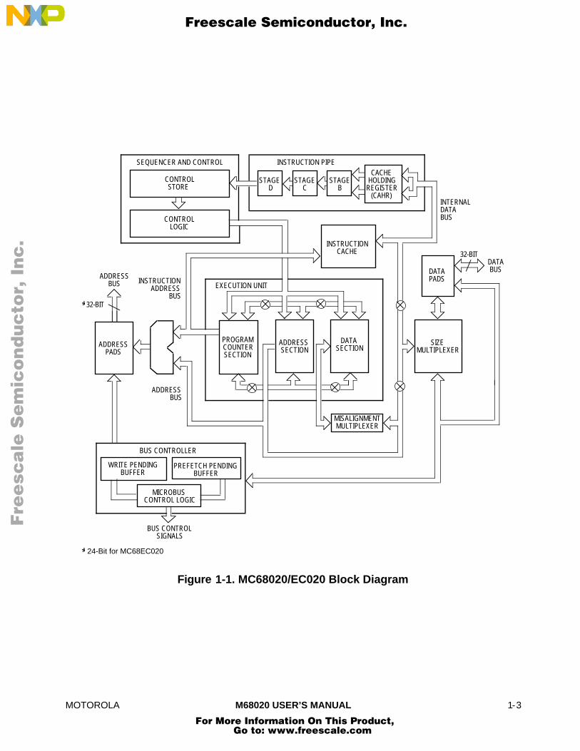
A block diagram of the MC68020/EC020 is shown in Figure 1-1.
Fre
esc
ale
Se
mic
on
du
cto
r, I
Freescale Semiconductor, Inc.
For More Information On This Product, Go to: www.freescale.com
nc
...
MOTOROLA M68020 USER’S MANUAL 1-3
SEQUENCER AND CONTROL
CONTROLSTORE
CONTROLLOGIC
INSTRUCTIONCACHE
STAGEB
STAGE C
STAGE D
CACHEHOLDING
REGISTER(CAHR)
INTERNALDATABUS
INSTRUCTION PIPE
INSTRUCTION ADDRESS
BUS
ADDRESSSECTION
PROGRAMCOUNTERSECTION
DATA SECTION
EXECUTION UNIT
MISALIGNMENTMULTIPLEXER
SIZEMULTIPLEXER
WRITE PENDINGBUFFER
PREFETCH PENDINGBUFFER
MICROBUS CONTROL LOGIC
BUS CONTROLLER
BUS CONTROLSIGNALS
ADDRESSBUS
ADDRESSPADS
DATAPADS
DATABUS
32-BIT
ADDRESSBUS
32-BIT*
* 24-Bit for MC68EC020
Figure 1-1. MC68020/EC020 Block Diagram
Fre
esc
ale
Se
mic
on
du
cto
r, I
Freescale Semiconductor, Inc.
For More Information On This Product, Go to: www.freescale.com
nc
...

1-4 M68020 USER’S MANUAL MOTOROLA
1.2 PROGRAMMING MODEL
The programming model of the MC68020/EC020 consists of two groups of registers, theuser model and the supervisor model, that correspond to the user and supervisor privilegelevels, respectively. User programs executing at the user privilege level use the registersof the user model. System software executing at the supervisor level uses the controlregisters of the supervisor level to perform supervisor functions.
As shown in the programming models (see Figures 1-2 and 1-3), the MC68020/EC020has 16 32-bit general-purpose registers, a 32-bit PC two 32-bit SSPs, a 16-bit SR, a 32-bitVBR, two 3-bit alternate function code registers, and two 32-bit cache handling (addressand control) registers.
The user programming model remains unchanged from earlier M68000 familymicroprocessors. The supervisor programming model supplements the user programmingmodel and is used exclusively by MC68020/EC020 system programmers who utilize thesupervisor privilege level to implement sensitive operating system functions. Thesupervisor programming model contains all the controls to access and enable the specialfeatures of the MC68020/EC020. All application software, written to run at thenonprivileged user level, migrates to the MC68020/EC020 from any M68000 platformwithout modification.
Registers D7–D0 are data registers used for bit and bit field (1 to 32 bits), byte (8 bit),word (16 bit), long-word (32 bit), and quad-word (64 bit) operations. Registers A6–A0 andthe USP, ISP, and MSP are address registers that may be used as software stackpointers or base address registers. Register A7 (shown as A7 in Figure 1-2 and as A7 ′and A7″ in Figure 1-3) is a register designation that applies to the USP in the userprivilege level and to either the ISP or MSP in the supervisor privilege level. In thesupervisor privilege level, the active stack pointer (interrupt or master) is called the SSP.In addition, the address registers may be used for word and long-word operations. All ofthe 16 general-purpose registers (D7–D0, A7–A0) may be used as index registers.
The PC contains the address of the next instruction to be executed by theMC68020/EC020. During instruction execution and exception processing, the processorautomatically increments the contents of the PC or places a new value in the PC, asappropriate.
Fre
esc
ale
Se
mic
on
du
cto
r, I
Freescale Semiconductor, Inc.
For More Information On This Product, Go to: www.freescale.com
nc
...

MOTOROLA M68020 USER’S MANUAL 1-5
078151631
D0
D1
D2
D3
D4
D5
D6
D7
DATAREGISTERS
0151631
A0
A1
A2
A3
A4
A5
A6
ADDRESSREGISTERS
0151631
A7 (USP)
PC
CCRCONDITION CODEREGISTER
78
031
15
0
PROGRAMCOUNTER
USER STACKPOINTER
0
Figure 1-2. User Programming Model
Fre
esc
ale
Se
mic
on
du
cto
r, I
Freescale Semiconductor, Inc.
For More Information On This Product, Go to: www.freescale.com
nc
...

1-6 M68020 USER’S MANUAL MOTOROLA
0
78
151631
SR
VBR
031
CACR
CAAR
031CACHE ADDRESSREGISTER
CACHE CONTROLREGISTER
1516
15
0
0
0
31
(CCR)
023
31
31
SFC
A7' (ISP)
A7'' (MSP)
INTERRUPT STACKPOINTER
MASTER STACKPOINTER
STATUSREGISTER
VECTOR BASEREGISTER
DFC
ALTERNATE FUNCTION CODEREGISTERS
Figure 1-3. Supervisor Programming Model Supplement
Fre
esc
ale
Se
mic
on
du
cto
r, I
Freescale Semiconductor, Inc.
For More Information On This Product, Go to: www.freescale.com
nc
...

MOTOROLA M68020 USER’S MANUAL 1-7
The SR (see Figure 1-4) stores the processor status. It contains the condition codes thatreflect the results of a previous operation and can be used for conditional instructionexecution in a program. The condition codes are extend (X), negative (N), zero (Z),overflow (V), and carry (C). The user byte, which contains the condition codes, is the onlyportion of the SR information available in the user privilege level, and it is referenced asthe CCR in user programs. In the supervisor privilege level, software can access the entireSR, including the interrupt priority mask (three bits) and control bits that indicate whetherthe processor is in:
1. One of two trace modes (T1, T0)
2. Supervisor or user privilege level (S)
3. Master or interrupt mode (M)
015
C
1
V
2
Z
3
N
4
X
5
0
6
0
7
0
8
I0
9
I1
10
I2
11
0
12
M
13
S
14
T0T1
SYSTEM BYTEUSER BYTE
(CONDITION CODE REGISTER)
TRACEENABLE
INTERRUPTPRIORITY MASK
SUPERVISOR/USER LEVEL
MASTER/INTERRUPT MODE
CARRY
OVERFLOW
ZERO
NEGATIVE
EXTEND
Figure 1-4. Status Register (SR)
The VBR contains the base address of the exception vector table in memory. Thedisplacement of an exception vector is added to the value in this register to access thevector table.
The alternate function code registers, SFC and DFC, contain 3-bit function codes. For theMC68020, function codes can be considered extensions of the 32-bit linear address thatoptionally provide as many as eight 4-Gbyte address spaces; for the MC68EC020,function codes can be considered extensions of the 24-bit linear address that optionallyprovide as many as eight 16-Mbyte address spaces. Function codes are automaticallygenerated by the processor to select address spaces for data and program at the userand supervisor privilege levels and to select a CPU address space for processor functions(e.g., coprocessor communications). Registers SFC and DFC are used by certaininstructions to explicitly specify the function codes for operations.
The CACR controls the on-chip instruction cache of the MC68020/EC020. The CAARstores an address for cache control functions.
Fre
esc
ale
Se
mic
on
du
cto
r, I
Freescale Semiconductor, Inc.
For More Information On This Product, Go to: www.freescale.com
nc
...

1-8 M68020 USER’S MANUAL MOTOROLA
1.3 DATA TYPES AND ADDRESSING MODES OVERVIEW
For detailed information on the data types and addressing modes supported by theMC68020/EC020, refer to M68000PM/AD, M68000 Family Programmer’s ReferenceManual.
The MC68020/EC020 supports seven basic data types:1. Bits
2. Bit Fields (Fields of consecutive bits, 1–32 bits long)
3. BCD Digits (Packed: 2 digits/byte, Unpacked: 1 digit/byte)
4. Byte Integers (8 bits)
5. Word Integers (16 bits)
6. Long-Word Integers (32 bits)
7. Quad-Word Integers (64 bits)
In addition, the MC68020/EC020 instruction set supports operations on other data typessuch as memory addresses. The coprocessor mechanism allows direct support of floating-point operations with the MC68881 and MC68882 floating-point coprocessors as well asspecialized user-defined data types and functions.
The 18 addressing modes listed in Table 1-1 include nine basic types:1. Register Direct
2. Register Indirect
3. Register Indirect with Index
4. Memory Indirect
5. PC Indirect with Displacement
6. PC Indirect with Index
7. PC Memory Indirect
8. Absolute
9. Immediate
The register indirect addressing modes have postincrement, predecrement, displacement,and index capabilities. The PC modes have index and offset capabilities. Both modes areextended to provide indirect reference through memory. In addition to these addressingmodes, many instructions implicitly specify the use of the CCR, stack pointer, and/or PC.
Fre
esc
ale
Se
mic
on
du
cto
r, I
Freescale Semiconductor, Inc.
For More Information On This Product, Go to: www.freescale.com
nc
...

MOTOROLA M68020 USER’S MANUAL 1-9
Table 1-1. Addressing Modes
Addressing Modes Syntax
Register DirectDataAddress
DnAn
Register IndirectAddressAddress with PostincrementAddress with PredecrementAddress with Displacement
(An)(An)+–(An)
(d16, An)
Address Register Indirect with Index8-Bit DisplacementBase Displacement
(d8, An, Xn)(bd, An, Xn)
Memory IndirectPostindexedPreindexed
([bd, An], Xn, od)([bd, An, Xn], od)
PC Indirect with Displacement (d16, PC)
PC Indirect with Index8-Bit DisplacementBase Displacement
(d8, PC, Xn)(bd, PC, Xn)
PC IndirectPostindexedPreindexed
([bd, PC], Xn, od)([bd, PC, Xn], od)
Absolute Data AddressingShortLong
(xxx).W(xxx).L
Immediate #<data>
NOTE:Dn = Data Register, D7–D0An = Address Register, A7–A0
d8, d16 = A twos complement or sign-extended displacement added as partof the effective address calculation; size is 8 (d8) or 16 (d16) bits;when omitted, assemblers use a value of zero.
Xn = Address or data register used as an index register; form isXn.SIZE*SCALE, where SIZE is .W or .L (indicates index registersize) and SCALE is 1, 2, 4, or 8 (index register is multiplied bySCALE); use of SIZE and/or SCALE is optional.
bd = A twos-complement base displacement; when present, size can be16 or 32 bits.
od = Outer displacement added as part of effective address calculationafter any memory indirection; use is optional with a size of 16 or 32bits.
PC = Program Counter<data> = Immediate value of 8, 16, or 32 bits
( ) = Effective Address[ ] = Use as indirect access to long-word address.
Fre
esc
ale
Se
mic
on
du
cto
r, I
Freescale Semiconductor, Inc.
For More Information On This Product, Go to: www.freescale.com
nc
...

1-10 M68020 USER’S MANUAL MOTOROLA
1.4 INSTRUCTION SET OVERVIEW
For detailed information on the MC68020/EC020 instruction set, refer to M68000PM/AD,M68000 Family Programmer’s Reference Manual.
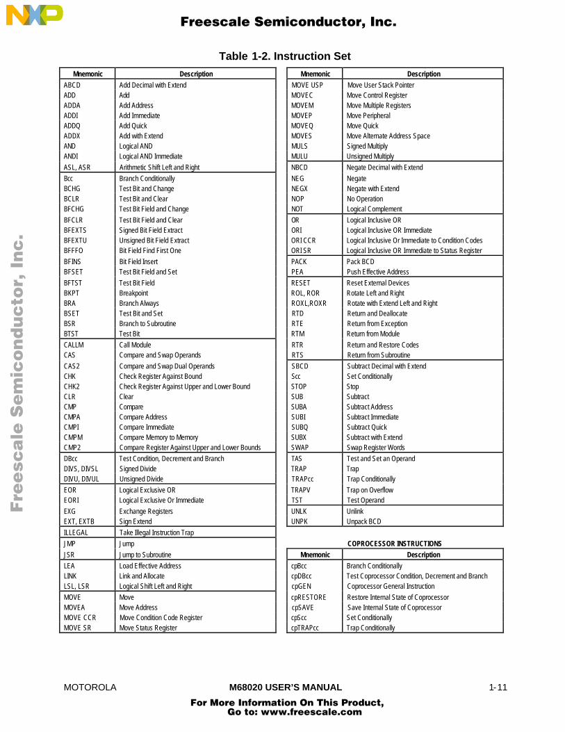
The instructions in the MC68020/EC020 instruction set are listed in Table 1-2. Theinstruction set has been tailored to support structured high-level languages andsophisticated operating systems. Many instructions operate on bytes, words, or longwords, and most instructions can use any of the 18 addressing modes.
1.5 VIRTUAL MEMORY AND VIRTUAL MACHINE CONCEPTS
The full addressing range of the MC68020 is 4 Gbytes (4,294,967,296 bytes) in each ofeight address spaces; the full addressing range of the MC68EC020 is 16 Mbytes(16,777,216 bytes) in each of the eight address spaces. Even though most systemsimplement a smaller physical memory, the system can be made to appear to have a full 4Gbytes (MC68020) or 16 Mbytes (MC68EC020) of memory available to each userprogram by using virtual memory techniques.
In a virtual memory system, a user program can be written as if it has a large amount ofmemory available, although the physical memory actually present is much smaller.Similarly, a system can be designed to allow user programs to access devices that are notphysically present in the system, such as tape drives, disk drives, printers, terminals, andso forth. With proper software emulation, a physical system can appear to be any otherM68000 computer system to a user program, and the program can be given full access toall of the resources of that emulated system. Such an emulated system is called a virtualmachine.
1.5.1 Virtual Memory
A system that supports virtual memory has a limited amount of high-speed physicalmemory that can be accessed directly by the processor and maintains an image of amuch larger virtual memory on a secondary storage device such as a large-capacity diskdrive. When the processor attempts to access a location in the virtual memory map that isnot resident in physical memory, a page fault occurs. The access to that location istemporarily suspended while the necessary data is fetched from secondary storage andplaced in physical memory. The suspended access is then either restarted or continued.
The MC68020/EC020 uses instruction continuation to support virtual memory. When abus cycle is terminated with a bus error, the microprocessor suspends the currentinstruction and executes the virtual memory bus error handler. When the bus error handlerhas completed execution, it returns control to the program that was executing when theerror was detected, reruns the faulted bus cycle (when required), and continues thesuspended instruction.
Fre
esc
ale
Se
mic
on
du
cto
r, I
Freescale Semiconductor, Inc.
For More Information On This Product, Go to: www.freescale.com
nc
...
MOTOROLA M68020 USER’S MANUAL 1-11
Table 1-2. Instruction Set
Mnemonic Description Mnemonic Description
ABCD Add Decimal with Extend MOVE USP Move User Stack PointerADD Add MOVEC Move Control RegisterADDA Add Address MOVEM Move Multiple RegistersADDI Add Immediate MOVEP Move PeripheralADDQ Add Quick MOVEQ Move QuickADDX Add with Extend MOVES Move Alternate Address SpaceAND Logical AND MULS Signed MultiplyANDI Logical AND Immediate MULU Unsigned Multiply
ASL, ASR Arithmetic Shift Left and Right NBCD Negate Decimal with Extend
Bcc Branch Conditionally NEG NegateBCHG Test Bit and Change NEGX Negate with ExtendBCLR Test Bit and Clear NOP No OperationBFCHG Test Bit Field and Change NOT Logical Complement
BFCLR Test Bit Field and Clear OR Logical Inclusive ORBFEXTS Signed Bit Field Extract ORI Logical Inclusive OR ImmediateBFEXTU Unsigned Bit Field Extract ORI CCR Logical Inclusive Or Immediate to Condition CodesBFFFO Bit Field Find First One ORI SR Logical Inclusive OR Immediate to Status Register
BFINS Bit Field Insert PACK Pack BCDBFSET Test Bit Field and Set PEA Push Effective Address
BFTST Test Bit Field RESET Reset External DevicesBKPT Breakpoint ROL, ROR Rotate Left and RightBRA Branch Always ROXL,ROXR Rotate with Extend Left and RightBSET Test Bit and Set RTD Return and DeallocateBSR Branch to Subroutine RTE Return from ExceptionBTST Test Bit RTM Return from Module
CALLM Call Module RTR Return and Restore CodesCAS Compare and Swap Operands RTS Return from Subroutine
CAS2 Compare and Swap Dual Operands SBCD Subtract Decimal with ExtendCHK Check Register Against Bound Scc Set ConditionallyCHK2 Check Register Against Upper and Lower Bound STOP StopCLR Clear SUB SubtractCMP Compare SUBA Subtract AddressCMPA Compare Address SUBI Subtract ImmediateCMPI Compare Immediate SUBQ Subtract QuickCMPM Compare Memory to Memory SUBX Subtract with ExtendCMP2 Compare Register Against Upper and Lower Bounds SWAP Swap Register Words
DBcc Test Condition, Decrement and Branch TAS Test and Set an OperandDIVS, DIVSL Signed Divide TRAP TrapDIVU, DIVUL Unsigned Divide TRAPcc Trap Conditionally
EOR Logical Exclusive OR TRAPV Trap on OverflowEORI Logical Exclusive Or Immediate TST Test Operand
EXG Exchange Registers UNLK UnlinkEXT, EXTB Sign Extend UNPK Unpack BCD
ILLEGAL Take Illegal Instruction Trap
JMP Jump COPROCESSOR INSTRUCTIONS
JSR Jump to Subroutine Mnemonic Description
LEA Load Effective Address cpBcc Branch ConditionallyLINK Link and Allocate cpDBcc Test Coprocessor Condition, Decrement and BranchLSL, LSR Logical Shift Left and Right cpGEN Coprocessor General Instruction
MOVE Move cpRESTORE Restore Internal State of CoprocessorMOVEA Move Address cpSAVE Save Internal State of CoprocessorMOVE CCR Move Condition Code Register cpScc Set ConditionallyMOVE SR Move Status Register cpTRAPcc Trap Conditionally
Fre
esc
ale
Se
mic
on
du
cto
r, I
Freescale Semiconductor, Inc.
For More Information On This Product, Go to: www.freescale.com
nc
...

1-12 M68020 USER’S MANUAL MOTOROLA
1.5.2 Virtual Machine
A typical use for a virtual machine system is the development of software, such as anoperating system, for a new machine also under development and not yet available forprogramming use. In a virtual machine system, a governing operating system emulatesthe hardware of the new machine and allows the new software to be executed anddebugged as though it were running on the new hardware. Since the new software iscontrolled by the governing operating system, it is executed at a lower privilege level thanthe governing operating system. Thus, any attempts by the new software to use virtualresources that are not physically present (and should be emulated) are trapped to thegoverning operating system and performed by its software.
In the MC68020/EC020 implementation of a virtual machine, the virtual application runs atthe user privilege level. The governing operating system executes at the supervisorprivilege level and any attempt by the new operating system to access supervisorresources or execute privileged instructions causes a trap to the governing operatingsystem.
Instruction continuation is used to support virtual I/O devices in memory-mappedinput/output systems. Control and data registers for the virtual device are simulated in thememory map. An access to a virtual register causes a fault, and the function of theregister is emulated by software.
1.6 PIPELINED ARCHITECTURE
The MC68020/EC020 contains a three-word instruction pipe where instruction opcodesare decoded. As shown in Figure 1-5, instruction words (instruction operation words andall extension words) enter the pipe at stage B and proceed to stages C and D. Aninstruction word is completely decoded when it reaches stage D of the pipe. Each stagehas a status bit that reflects whether the word in the stage was loaded with data from abus cycle that was terminated abnormally. Stages of the pipe are only filled in response tospecific prefetch requests issued by the sequencer.
Words are loaded into the instruction pipe from the cache holding register. Although theindividual stages of the pipe are only 16 bits wide, the cache holding register is 32 bitswide and contains the entire long word. This long word is obtained from the instructioncache or the external bus in response to a prefetch request from the sequencer. When thesequencer requests an even-word (long-word-aligned) prefetch, the entire long word isaccessed from the instruction cache or the external bus and loaded into the cache holdingregister, and the high-order word is also loaded into stage B of the pipe. The instructionword for the next sequential prefetch can then be accessed directly from the cacheholding register, and no external bus cycle or instruction cache access is required. Thecache holding register provides instruction words to the pipe regardless of whether theinstruction cache is enabled or disabled.
Fre
esc
ale
Se
mic
on
du
cto
r, I
Freescale Semiconductor, Inc.
For More Information On This Product, Go to: www.freescale.com
nc
...

MOTOROLA M68020 USER’S MANUAL 1-13
SEQUENCER
CACHEHOLDING
REGISTER
CONTROLUNIT
EXECUTIONUNIT
STAGED
INSTRUCTION PIPE
STAGEC
STAGEB
INSTRUCTIONFLOW FROMCACHE AND
MEMORY
Figure 1-5. Instruction Pipe
The sequencer is either executing microinstructions or awaiting completion of accessesthat are necessary to continue executing microcode. The bus controller is responsible forall bus activity. The sequencer controls the bus controller, instruction execution, andinternal processor operations such as the calculation of effective addresses and thesetting of condition codes. The sequencer initiates instruction word prefetches andcontrols the validation of instruction words in the instruction pipe.
Prefetch requests are simultaneously submitted to the cache holding register, theinstruction cache, and the bus controller. Thus, even if the instruction cache is disabled,an instruction prefetch may hit in the cache holding register and cause an external buscycle to be aborted.
1.7 CACHE MEMORY
Due to locality of reference, instructions that are used in a program have a high probabilityof being reused within a short time. Additionally, instructions that reside in proximity to theinstructions currently in use also have a high probability of being utilized within a shortperiod. To exploit these locality characteristics, the MC68020/EC020 contains an on-chipinstruction cache.
The cache improves the overall performance of the system by reducing the number of buscycles required by the processor to fetch information from memory and by increasing thebus bandwidth available for other bus masters in the system.
Fre
esc
ale
Se
mic
on
du
cto
r, I
Freescale Semiconductor, Inc.
For More Information On This Product, Go to: www.freescale.com
nc
...
MOTOROLA M68020 USER’S MANUAL 2-1
SECTION 2PROCESSING STATES
This section describes the processing states of the MC68020/EC020. It describes thefunctions of the bits in the supervisor portion of the SR and the actions taken by theprocessor in response to exception conditions.
Unless the processor has halted, it is always in either the normal or the exceptionprocessing state. Whenever the processor is executing instructions or fetching instructionsor operands, it is in the normal processing state. The processor is also in the normalprocessing state while it is storing instruction results or communicating with acoprocessor.
NOTE
Exception processing refers specifically to the transition fromnormal processing of a program to normal processing ofsystem routines, interrupt routines, and other exceptionhandlers. Exception processing includes all stackingoperations, the fetch of the exception vector, and the filling ofthe instruction pipe caused by an exception. Exceptionprocessing has completed when execution of the firstinstruction of the exception handler routine begins.
The processor enters the exception processing state when an interrupt is acknowledged,when an instruction is traced or results in a trap, or when some other exception conditionarises. Execution of certain instructions or unusual conditions occurring during theexecution of any instruction can cause exceptions. External conditions, such as interrupts,bus errors, and some coprocessor responses, also cause exceptions. Exceptionprocessing provides an efficient transfer of control to handlers and routines that processthe exceptions.
A catastrophic system failure occurs whenever the processor receives a bus error orgenerates an address error while in the exception processing state. This type of failurehalts the processor. For example, if during the exception processing of one bus erroranother bus error occurs, the MC68020/EC020 has not completed the transition to normalprocessing and has not completed saving the internal state of the machine; therefore, theprocessor assumes that the system is not operational and halts. Only an external resetcan restart a halted processor. (When the processor executes a STOP instruction, it is in aspecial type of normal processing state—one without bus cycles. It is stopped, not halted.)
Fre
esc
ale
Se
mic
on
du
cto
r, I
Freescale Semiconductor, Inc.
For More Information On This Product, Go to: www.freescale.com
nc
...

2-2 M68020 USER’S MANUAL MOTOROLA
2.1 PRIVILEGE LEVELS
The processor operates at one of two privilege levels: the user level or the supervisorlevel. The supervisor level has higher privileges than the user level. Not all processor orcoprocessor instructions are permitted to execute at the lower privileged user level, but allare available at the supervisor level. This arrangement allows a separation of supervisorand user so the supervisor can protect system resources from uncontrolled access. TheS-bit in the SR is used to select either the user or supervisor privilege level and either theUSP or an SSP for stack operations. The processor identifies a bus access (supervisor oruser mode) via the function codes so that differentiation between supervisor level anduser level can be maintained.
In many systems, the majority of programs execute at the user level. User programs canaccess only their own code and data areas and can be restricted from accessing otherinformation. The operating system typically executes at the supervisor privilege level. Ithas access to all resources, performs the overhead tasks for the user-level programs, andcoordinates user-level program activities.
2.1.1 Supervisor Privilege Level
The supervisor level is the higher privilege level. The privilege level is determined by theS-bit of the SR; if the S-bit is set, the supervisor privilege level applies, and all instructionsare executable. The bus cycles for instructions executed at the supervisor level arenormally classified as supervisor references, and the values of the FC2–FC0 signals referto supervisor address spaces.
In a multitasking operating system, it is more efficient to have a supervisor stack spaceassociated with each user task and a separate stack space for interrupt-associated tasks.The MC68020/EC020 provides two supervisor stacks, master and interrupt; the M bit ofthe SR selects which of the two is active. When the M-bit is set, references to the SSPimplicitly or to address register seven (A7) explicitly, access the MSP. The operatingsystem sets the MSP for each task to point to a task-related area of supervisor dataspace. This arrangement separates task-related supervisor activity from asynchronous,I/O-related supervisor tasks that may be only coincidental to the currently executing task.The MSP can separately maintain task control information for each currently executinguser task, and the software updates the MSP when a task switch is performed, providingan efficient means for transferring task-related stack items. The other supervisor stackpointer, the ISP, can be used for interrupt control information and workspace area asinterrupt handling routines require.
When the M-bit is clear, the MC68020/EC020 is in the interrupt mode of the supervisorprivilege level, and operation is the same as supervisor mode in the MC68000,MC68HC001, MC68008, and MC68010. (The processor is in this mode after a resetoperation.) All SSP references access the ISP in this mode.
Fre
esc
ale
Se
mic
on
du
cto
r, I
Freescale Semiconductor, Inc.
For More Information On This Product, Go to: www.freescale.com
nc
...

MOTOROLA M68020 USER’S MANUAL 2-3
The value of the M-bit in the SR does not affect execution of privileged instructions; bothmaster and interrupt modes are at the supervisor privilege level. Instructions that affect theM-bit are MOVE to SR, ANDI to SR, EORI to SR, ORI to SR, and RTE. Also, theprocessor automatically saves the M-bit value and clears it in the SR as part of exceptionprocessing for interrupts.
All exception processing is performed at the supervisor privilege level. All bus cyclesgenerated during exception processing are supervisor references, and all stack accessesuse the active SSP.
2.1.2 User Privilege Level
The user level is the lower privilege level. The privilege level is determined by the S-bit ofthe SR; if the S-bit is clear, the processor executes instructions at the user privilege level.
Most instructions execute at either privilege level, but some instructions that haveimportant system effects are privileged and can only be executed at the supervisor level.For instance, user programs are not allowed to execute the STOP instruction or theRESET instruction. To prevent a user program from entering the supervisor privilege levelexcept in a controlled manner, instructions that can alter the S-bit in the SR are privileged.The TRAP #n instruction provides controlled access to operating system services for userprograms.
The bus cycles for an instruction executed at the user privilege level are classified as userreferences, and the values of the FC2–FC0 signals specify user address spaces. Whilethe processor is at the user level, references to the system stack pointer implicitly, or toaddress register seven (A7) explicitly, refer to the USP.
2.1.3 Changing Privilege Level
To change from the user to the supervisor privilege level, one of the conditions thatcauses the processor to perform exception processing must occur. This causes a changefrom the user level to the supervisor level and can cause a change from the master modeto the interrupt mode. Exception processing saves the current values of the S and M bitsof the SR (along with the rest of the SR) on the active supervisor stack, and then sets theS-bit, forcing the processor into the supervisor privilege level. When the exception beingprocessed is an interrupt and the M-bit is set, the M-bit is cleared, putting the processorinto the interrupt mode. Execution of instructions continues at the supervisor level toprocess the exception condition.
To return to the user privilege level, a system routine must execute one of the followinginstructions: MOVE to SR, ANDI to SR, EORI to SR, ORI to SR, or RTE. Theseinstructions execute at the supervisor privilege level and can modify the S-bit of the SR.After these instructions execute, the instruction pipeline is flushed and is refilled from theappropriate address space.
The RTE instruction returns to the program that was executing when the exceptionoccurred. It restores the exception stack frame saved on the supervisor stack. If the frame
Fre
esc
ale
Se
mic
on
du
cto
r, I
Freescale Semiconductor, Inc.
For More Information On This Product, Go to: www.freescale.com
nc
...
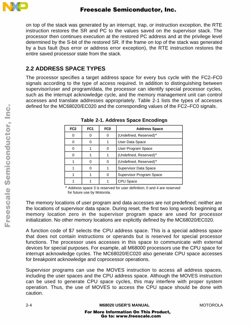
2-4 M68020 USER’S MANUAL MOTOROLA
on top of the stack was generated by an interrupt, trap, or instruction exception, the RTEinstruction restores the SR and PC to the values saved on the supervisor stack. Theprocessor then continues execution at the restored PC address and at the privilege leveldetermined by the S-bit of the restored SR. If the frame on top of the stack was generatedby a bus fault (bus error or address error exception), the RTE instruction restores theentire saved processor state from the stack.
2.2 ADDRESS SPACE TYPES
The processor specifies a target address space for every bus cycle with the FC2–FC0signals according to the type of access required. In addition to distinguishing betweensupervisor/user and program/data, the processor can identify special processor cycles,such as the interrupt acknowledge cycle, and the memory management unit can controlaccesses and translate addresses appropriately. Table 2-1 lists the types of accessesdefined for the MC68020/EC020 and the corresponding values of the FC2–FC0 signals.
Table 2-1. Address Space Encodings
FC2 FC1 FC0 Address Space
0 0 0 (Undefined, Reserved)*
0 0 1 User Data Space
0 1 0 User Program Space
0 1 1 (Undefined, Reserved)*
1 0 0 (Undefined, Reserved)*
1 0 1 Supervisor Data Space
1 1 0 Supervisor Program Space
1 1 1 CPU Space
* Address space 3 is reserved for user definition; 0 and 4 are reservedfor future use by Motorola.
The memory locations of user program and data accesses are not predefined; neither arethe locations of supervisor data space. During reset, the first two long words beginning atmemory location zero in the supervisor program space are used for processorinitialization. No other memory locations are explicitly defined by the MC68020/EC020.
A function code of $7 selects the CPU address space. This is a special address spacethat does not contain instructions or operands but is reserved for special processorfunctions. The processor uses accesses in this space to communicate with externaldevices for special purposes. For example, all M68000 processors use the CPU space forinterrupt acknowledge cycles. The MC68020/EC020 also generate CPU space accessesfor breakpoint acknowledge and coprocessor operations.
Supervisor programs can use the MOVES instruction to access all address spaces,including the user spaces and the CPU address space. Although the MOVES instructioncan be used to generate CPU space cycles, this may interfere with proper systemoperation. Thus, the use of MOVES to access the CPU space should be done withcaution.
Fre
esc
ale
Se
mic
on
du
cto
r, I
Freescale Semiconductor, Inc.
For More Information On This Product, Go to: www.freescale.com
nc
...

MOTOROLA M68020 USER’S MANUAL 2-5
2.3 EXCEPTION PROCESSING
An exception is defined as a special condition that preempts normal processing. Bothinternal and external conditions can cause exceptions. External conditions that causeexceptions are interrupts from external devices, bus errors, coprocessor-detected errors,and reset. Instructions, address errors, tracing, and breakpoints are internal conditionsthat cause exceptions. The TRAP, TRAPcc, TRAPV, cpTRAPcc, CHK, CHK2, RTE,BKPT, CALLM, RTM, cp RESTORE, DIVS and DIVU instructions can generate exceptionsas part of their normal execution. In addition, illegal instructions, privilege violations, andcoprocessor protocol violations cause exceptions.
Exception processing, which is the transition from the normal processing of a program tothe processing required for the exception condition, involves the exception vector tableand an exception stack frame. The following paragraphs describe the exception vectorsand a generalized exception stack frame. Exception processing is discussed in detail inSection 6 Exception Processing. Coprocessor-detected exceptions are discussed indetail in Section 7 Coprocessor Interface Description.
2.3.1 Exception Vectors
The VBR contains the base address of the 1024-byte exception vector table, whichconsists of 256 exception vectors. Exception vectors contain the memory addresses ofroutines that begin execution at the completion of exception processing. These routinesperform a series of operations appropriate for the corresponding exceptions. Because theexception vectors contain memory addresses, each consists of one long word, except forthe reset vector. The reset vector consists of two long words: the address used to initializethe ISP and the address used to initialize the PC.
The address of an exception vector is derived from an 8-bit vector number and the VBR.The vector numbers for some exceptions are obtained from an external device; others aresupplied automatically by the processor. The processor multiplies the vector number byfour to calculate the vector offset, which it adds to the VBR. The sum is the memoryaddress of the vector. All exception vectors are located in supervisor data space, exceptthe reset vector, which is located in supervisor program space. Only the initial reset vectoris fixed in the processor's memory map; once initialization is complete, there are no fixedassignments. Since the VBR provides the base address of the vector table, the vectortable can be located anywhere in memory; it can even be dynamically relocated for eachtask that is executed by an operating system. Details of exception processing are providedin Section 6 Exception Processing , and Table 6-1 lists the exception vectorassignments.
Fre
esc
ale
Se
mic
on
du
cto
r, I
Freescale Semiconductor, Inc.
For More Information On This Product, Go to: www.freescale.com
nc
...

2-6 M68020 USER’S MANUAL MOTOROLA
2.3.2 Exception Stack Frame
Exception processing saves the most volatile portion of the current processor context onthe top of the supervisor stack. This context is organized in a format called the exceptionstack frame. This information always includes a copy of the SR, the PC, the vector offsetof the vector, and the frame format field. The frame format field identifies the type of stackframe. The RTE instruction uses the value in the format field to properly restore theinformation stored in the stack frame and to deallocate the stack space. The general formof the exception stack frame is illustrated in Figure 2-1. Refer to Section 6 ExceptionProcessing for a complete list of exception stack frames.
015
SSP
12
FORMAT
STATUS REGISTER
PROGRAM COUNTER
VECTOR OFFSET
ADDITIONAL PROCESSOR STATE INFORMATION(2, 6, 12, OR 42 WORDS, IF NEEDED)
Figure 2-1. General Exception Stack Frame
Fre
esc
ale
Se
mic
on
du
cto
r, I
Freescale Semiconductor, Inc.
For More Information On This Product, Go to: www.freescale.com
nc
...
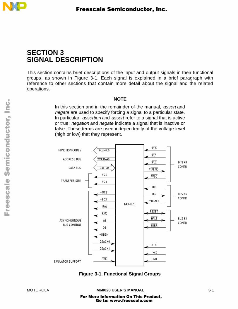
MOTOROLA M68020 USER’S MANUAL 3-1
SECTION 3SIGNAL DESCRIPTION
This section contains brief descriptions of the input and output signals in their functionalgroups, as shown in Figure 3-1. Each signal is explained in a brief paragraph withreference to other sections that contain more detail about the signal and the relatedoperations.
NOTE
In this section and in the remainder of the manual, assert andnegate are used to specify forcing a signal to a particular state.In particular, assertion and assert refer to a signal that is activeor true; negation and negate indicate a signal that is inactive orfalse. These terms are used independently of the voltage level(high or low) that they represent.
FC2–FC0
A31–A0
D31–D0
FUNCTION CODES
ADDRESS BUS
DATA BUS
TRANSFER SIZE
ASYNCHRONOUSBUS CONTROL
EMULATOR SUPPORT
BUS ARBCONTRO
INTERRUCONTRO
BUS EXCCONTRO
MC68020
SIZ0
SIZ1
OCS
ECS
R/W
RMC
AS
DS
DBEN
DSACK0
DSACK1
CDIS GND
V
CLK
BERR
HALT
RESET
BGACK
BG
BR
AVEC
IPEND
IPL2
IPL1
IPL0
CC
*
*
*
**
*
*
Figure 3-1. Functional Signal Groups
Fre
esc
ale
Se
mic
on
du
cto
r, I
Freescale Semiconductor, Inc.
For More Information On This Product, Go to: www.freescale.com
nc
...
3-2 M68020 USER’S MANUAL MOTOROLA
3.1 SIGNAL INDEX
The input and output signals for the MC68020/EC020 are listed in Table 3-1. Both thenames and mnemonics are shown along with brief signal descriptions. Signals that areimplemented in the MC68020, but not in the MC68EC020, have an asterisk (*) precedingthe signal name in Table 3-1. Also, note that the address bus is 32 bits wide for theMC68020 and 24 bits wide for the MC68EC020. For more detail on each signal, refer tothe paragraph in this section named for the signal and the reference in that paragraph to adescription of the related operations.
Timing specifications for the signals listed in Table 3-1 can be found in Section 10Electrical Characteristics.
3.2 FUNCTION CODE SIGNALS (FC2–FC0)
These three-state outputs identify the address space of the current bus cycle. Table 2-1shows the relationships of the function code signals to the privilege levels and the addressspaces. Refer to Section 2 Processing States for more information.
3.3 ADDRESS BUS (A31–A0, MC68020)(A23–A0, MC68EC020)
These three-state outputs provide the address for the current bus cycle, except in theCPU address space. Refer to Section 2 Processing States for more information on theCPU address space. A31 is the most significant address signal for the MC68020; A23 isthe most significant address signal for the MC68EC020. The upper eight bits (A31–A24)are used internally by the MC68EC020 to access the internal instruction cache addresstag. Refer to Section 5 Bus Operation for information on the address bus and itsrelationship to bus operation.
3.4 DATA BUS (D31–D0)
These three-state bidirectional signals provide the general-purpose data path between theMC68020/EC020 and all other devices. The data bus can transfer 8, 16, 24, or 32 bits ofdata per bus cycle. D31 is the most significant bit of the data bus. Refer to Section 5 BusOperation for more information on the data bus and its relationship to bus operation.
3.5 TRANSFER SIZE SIGNALS (SIZ1, SIZ0)
These three-state outputs indicate the number of bytes remaining to be transferred for thecurrent bus cycle. Signals A1, A0, DSACK1, DSACK0, SIZ1, and SIZ0 define the numberof bits transferred on the data bus. Refer to Section 5 Bus Operation for moreinformation on SIZ1 and SIZ0 and their use in dynamic bus sizing.
Fre
esc
ale
Se
mic
on
du
cto
r, I
Freescale Semiconductor, Inc.
For More Information On This Product, Go to: www.freescale.com
nc
...

MOTOROLA M68020 USER’S MANUAL 3-3
Table 3-1. Signal Index
Signal Name Mnemonic Function
Function Codes FC2–FC0 3-bit function code used to identify the address space of each bus cycle.
Address BusMC68020MC68EC020
A31–A0A23–A0
32-bit address bus24-bit address bus
Data Bus D31–D0 32-bit data bus used to transfer 8, 16, 24, or 32 bits of data per buscycle.
Size SIZ1, SIZ0 Indicates the number of bytes remaining to be transferred for this cycle.These signals, together with A1 and A0, define the active sections of thedata bus.
*External Cycle Start ECS Provides an indication that a bus cycle is beginning.
*Operand Cycle Start OCS Identical operation to that of ECS except that OCS is asserted only duringthe first bus cycle of an operand transfer.
Read/Write R/W Defines the bus transfer as a processor read or write.
Read-Modify-Write Cycle RMC Provides an indicator that the current bus cycle is part of an indivisibleread-modify-write operation.
Address Strobe AS Indicates that a valid address is on the bus.
Data Strobe DS Indicates that valid data is to be placed on the data bus by an externaldevice or has been placed on the data bus by the MC68020/EC020.
*Data Buffer Enable DBEN Provides an enable signal for external data buffers.
Data Transfer and SizeAcknowledge
DSACK1,DSACK0
Bus response signals that indicate the requested data transfer operationhas completed. In addition, these two lines indicate the size of theexternal bus port on a cycle-by-cycle basis and are used forasynchronous transfers.
Interrupt Priority Level IPL2–IPL0 Provides an encoded interrupt level to the processor.
*Interrupt Pending IPEND Indicates that an interrupt is pending.
Autovector AVEC Requests an autovector during an interrupt acknowledge cycle.
Bus Request BR Indicates that an external device requires bus mastership.
Bus Grant BG Indicates that an external device may assume bus mastership.
*Bus Grant Acknowledge BGACK Indicates that an external device has assumed bus mastership.
Reset RESET System reset.
Halt HALT Indicates that the processor should suspend bus activity or that theprocessor has halted due to a double bus fault.
Bus Error BERR Indicates that an erroneous bus operation is being attempted.
Cache Disable CDIS Statically disables the on-chip cache to assist emulator support.
Clock CLK Clock input to the processor.
Power Supply VCC Power supply.
Ground GND Ground connection.
*This signal is implemented in the MC68020 and not implemented in the MC68EC020.
Fre
esc
ale
Se
mic
on
du
cto
r, I
Freescale Semiconductor, Inc.
For More Information On This Product, Go to: www.freescale.com
nc
...
3-4 M68020 USER’S MANUAL MOTOROLA
3.6 ASYNCHRONOUS BUS CONTROL SIGNALS
The following signals control synchronous bus transfer operations for theMC68020/EC020. Note that OCS, ECS, and DBEN are implemented in MC68020 and notimplemented in the MC68EC020.
Operand Cycle Start (OCS, MC68020 only)This output signal indicates the beginning of the first external bus cycle for an instructionprefetch or a data operand transfer. OCS is not asserted for subsequent cycles that areperformed due to dynamic bus sizing or operand misalignment. Refer to Section 5 BusOperation for information about the relationship of OCS to bus operation.
OCS is not implemented in the MC68EC020.
External Cycle Start (ECS, MC68020 only)This output signal indicates the beginning of a bus cycle of any type. Refer to Section 5Bus Operation for information about the relationship of ECS to bus operation.
ECS is not implemented in the MC68EC020.
Read/Write (R/W)This three-state output signal defines the type of bus cycle. A high level indicates a readcycle; a low level indicates a write cycle. Refer to Section 5 Bus Operation forinformation about the relationship of R/W to bus operation.
Read-Modify-Write Cycle (RMC)This three-state output signal identifies the current bus cycle as part of an indivisibleread-modify-write operation; it remains asserted during all bus cycles of the read-modify-write operation. Refer to Section 5 Bus Operation for information about therelationship of RMC to bus operation.
Address Strobe (AS)This three-state output signal indicates that a valid address is on the address bus. TheFC2–FC0, SIZ1, SIZ0, and R/W signals are also valid when AS is asserted. Refer toSection 5 Bus Operation for information about the relationship of AS to bus operation.
Data Strobe (DS)During a read cycle, this three-state output signal indicates that an external deviceshould place valid data on the data bus. During a write cycle, DS indicates that theMC68020/EC020 has placed valid data on the bus. During two-clock synchronous writecycles, the MC68020/EC020 does not assert DS. Refer to Section 5 Bus Operation formore information about the relationship of DS to bus operation.
Fre
esc
ale
Se
mic
on
du
cto
r, I
Freescale Semiconductor, Inc.
For More Information On This Product, Go to: www.freescale.com
nc
...

MOTOROLA M68020 USER’S MANUAL 3-5
Data Buffer Enable (DBEN, MC68020 only)This output signal is an enable signal for external data buffers. This signal may not berequired in all systems. Refer to Section 5 Bus Operation for more information aboutthe relationship of DBEN to bus operation.
DBEN is not implemented in the MC68EC020.
Data Transfer and Size Acknowledge (DSACK1, DSACK0)These input signals indicate the completion of a requested data transfer operation. Inaddition, they indicate the size of the external bus port at the completion of each cycle.These signals apply only to asynchronous bus cycles. Refer to Section 5 BusOperation for more information on these signals and their relationship to dynamic bussizing.
3.7 INTERRUPT CONTROL SIGNALS
The following signals are the interrupt control signals for the MC68020/EC020. Note thatIPEND is implemented in the MC68020 and not implemented in the MC68EC020.
Interrupt Priority Level Signals (IPL2–IPL0)These input signals provide an indication of an interrupt condition and the encoding ofthe interrupt level from a peripheral or external prioritizing circuitry. IPL2 is the mostsignificant bit of the level number. For example, since the IPL2–IPL0 signals are activelow, IPL2–IPL0 equal to $5 corresponds to an interrupt request at interrupt level 2.Refer to Section 6 Exception Processing for information on MC68020/EC020interrupts.
Interrupt Pending (IPEND, MC68020 only)This output signal indicates that an interrupt request exceeding the current interruptpriority mask in the SR has been recognized internally. This output is for use by externaldevices (coprocessors and other bus masters, for example) to predict processoroperation on the following instruction boundaries. Refer to Section 6 ExceptionProcessing for interrupt information. Also, refer to Section 5 Bus Operation for businformation related to interrupts.
IPEND is not implemented in the MC68EC020.
Autovector (AVEC)This input signal indicates that the MC68020/EC020 should generate an automaticvector during an interrupt acknowledge cycle. Refer to Section 5 Bus Operation formore information about automatic vectors.
Fre
esc
ale
Se
mic
on
du
cto
r, I
Freescale Semiconductor, Inc.
For More Information On This Product, Go to: www.freescale.com
nc
...
3-6 M68020 USER’S MANUAL MOTOROLA
3.8 BUS ARBITRATION CONTROL SIGNALS
The following signals are the bus arbitration control signals used to determine whichdevice in a system is the bus master. Note that BGACK is implemented in the MC68020and not implemented in the MC68EC020.
Bus Request (BR)This input signal indicates that an external device needs to become the bus master. BRis typically a “wire-ORed” input (but does not need to be constructed from open-collectordevices). Refer to Section 5 Bus Operation for more information on MC68020 busarbitration. Refer to Section 5 Bus Operation and Appendix A Interfacing anMC68EC020 to a DMA Device That Supports a Three-Wire Bus ArbitrationProtocol for more information on MC68EC020 bus arbitration.
Bus Grant (BG)This output signal indicates that the MC68020/EC020 will release ownership of the buswhen the current processor bus cycle completes. Refer to Section 5 Bus Operation formore information on MC68020 bus arbitration. Refer to Section 5 Bus Operation andAppendix A Interfacing an MC68EC020 to a DMA Device That Supports a Three-Wire Bus Arbitration Protocol for more information on MC68EC020 bus arbitration.
Bus Grant Acknowledge (BGACK, MC68020 only)This input signal indicates that an external device has become the bus master. Refer toSection 5 Bus Operation for more information on MC68020 bus arbitration. Refer toSection 5 Bus Operation and Appendix A Interfacing an MC68EC020 to a DMADevice That Supports a Three-Wire Bus Arbitration Protocol for more informationon MC68EC020 bus arbitration.
BGACK is not implemented in the MC68EC020.
3.9 BUS EXCEPTION CONTROL SIGNALS
The following signals are the bus exception control signals for the MC68020/EC020.
Reset (RESET)This bidirectional open-drain signal is used to initiate a system reset. An external resetsignal resets the MC68020/EC020 as well as all external devices. A reset signal fromthe processor (asserted as part of the RESET instruction) resets external devices only;the internal state of the processor is not altered. Refer to Section 5 Bus Operation fora description of reset bus operation and Section 6 Exception Processing forinformation about the reset exception.
Fre
esc
ale
Se
mic
on
du
cto
r, I
Freescale Semiconductor, Inc.
For More Information On This Product, Go to: www.freescale.com
nc
...
MOTOROLA M68020 USER’S MANUAL 3-7
Halt (HALT)The assertion of this bidirectional open-drain signal indicates that the processor shouldsuspend bus activity or, when used with BERR, that the processor should retry thecurrent cycle. Refer to Section 5 Bus Operation for a description of the effects ofHALT on bus operations. When the processor has stopped executing instructions dueto a double bus fault condition, the HALT line is asserted by the processor to indicate toexternal devices that the processor has stopped.
Bus Error (BERR)This input signal indicates that an invalid bus operation is being attempted or, whenused with HALT, that the processor should retry the current cycle. Refer to Section 5Bus Operation for a description of the effects of BERR on bus operations.
3.10 EMULATOR SUPPORT SIGNAL
The following signal supports emulation by providing a means for an emulator to disablethe on-chip cache by supplying internal status information to an emulator. Refer toSection 7 Coprocessor Interface Description for more detailed information onemulation support.
Cache Disable (CDIS)This input signal statically disables the on-chip cache to assist emulator support. Referto Section 4 On-Chip Cache Memory for information about the cache; refer to Section9 Applications Information for a description of the use of this signal by an emulator.CDIS does not flush the instruction cache; entries remain unaltered and becomeavailable again when CDIS is negated.
3.11 CLOCK (CLK)
The CLK signal is the clock input to the MC68020/EC020. This TTL-compatible signalshould not be gated off at any time while power is applied to the processor. Refer toSection 9 Applications Information for suggestions on clock generation. Refer toSection 10 Electrical Characteristics for electrical characteristics.
3.12 POWER SUPPLY CONNECTIONS
The MC68020/EC020 requires connection to a VCC power supply, positive with respect toground. The VCC connections are grouped to supply adequate current for the varioussections of the processor. The ground connections are similarly grouped. Section 11Ordering Information and Mechanical Data describes the groupings of VCC and groundconnections, and Section 9 Applications Information describes a typical power supplyinterface.
Fre
esc
ale
Se
mic
on
du
cto
r, I
Freescale Semiconductor, Inc.
For More Information On This Product, Go to: www.freescale.com
nc
...
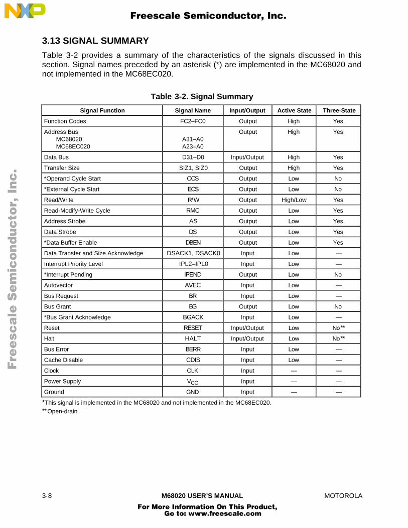
3-8 M68020 USER’S MANUAL MOTOROLA
3.13 SIGNAL SUMMARY
Table 3-2 provides a summary of the characteristics of the signals discussed in thissection. Signal names preceded by an asterisk (*) are implemented in the MC68020 andnot implemented in the MC68EC020.
Table 3-2. Signal Summary
Signal Function Signal Name Input/Output Active State Three-State
Function Codes FC2–FC0 Output High Yes
Address BusMC68020MC68EC020
A31–A0A23–A0
Output High Yes
Data Bus D31–D0 Input/Output High Yes
Transfer Size SIZ1, SIZ0 Output High Yes
*Operand Cycle Start OCS Output Low No
*External Cycle Start ECS Output Low No
Read/Write R/W Output High/Low Yes
Read-Modify-Write Cycle RMC Output Low Yes
Address Strobe AS Output Low Yes
Data Strobe DS Output Low Yes
*Data Buffer Enable DBEN Output Low Yes
Data Transfer and Size Acknowledge DSACK1, DSACK0 Input Low —
Interrupt Priority Level IPL2–IPL0 Input Low —
*Interrupt Pending IPEND Output Low No
Autovector AVEC Input Low —
Bus Request BR Input Low —
Bus Grant BG Output Low No
*Bus Grant Acknowledge BGACK Input Low —
Reset RESET Input/Output Low No**
Halt HALT Input/Output Low No**
Bus Error BERR Input Low —
Cache Disable CDIS Input Low —
Clock CLK Input — —
Power Supply VCC Input — —
Ground GND Input — —
*This signal is implemented in the MC68020 and not implemented in the MC68EC020.**Open-drain
Fre
esc
ale
Se
mic
on
du
cto
r, I
Freescale Semiconductor, Inc.
For More Information On This Product, Go to: www.freescale.com
nc
...
MOTOROLA M68020 USER’S MANUAL 4-1
SECTION 4ON-CHIP CACHE MEMORY
The MC68020/EC020 incorporates an on-chip cache memory as a means of improvingperformance. The cache is implemented as a CPU instruction cache and is used to storethe instruction stream prefetch accesses from the main memory.
An increase in instruction throughput results when instruction words required by aprogram are available in the on-chip cache and the time required to access them on theexternal bus is eliminated. In systems with more than one bus master (e.g., a processorand a DMA device), reduced external bus activity increases overall performance byincreasing the availability of the bus for use by external devices without degrading theperformance of the MC68020/EC020.
4.1 ON-CHIP CACHE ORGANIZATION AND OPERATION
The MC68020/EC020 on-chip instruction cache is a direct-mapped cache of 64 long-wordentries. Each cache entry consists of a tag field (A31–A8 and FC2), one valid bit, and 32bits (two words) of instruction data. Figure 4-1 shows a block diagram of the on-chipcache organization.
Externally, the MC68EC020 does not use the upper eight bits of the address (A31–A24),and addresses $FF000000 and $00000000 from the MC68EC020 appear the same.However, the MC68EC020 does use A31–A24 internally in the instruction cache addresstag, and addresses $FF000000 and $00000000 appear different in the MC68EC020instruction cache. The MC68020, MC68030/EC030, and MC68040/EC040 use all 32 bitsof the address externally. To maintain object-code upgrade compatibility when designingwith the MC68EC020, the upper eight bits should be considered part of the address whenassigning address spaces in hardware.
When enabled, the MC68020/EC020 instruction cache is used to store instructionprefetches (instruction words and extension words) as they are requested by the CPU.Instruction prefetches are normally requested from sequential memory addresses exceptwhen a change of program flow occurs (e.g., a branch taken) or when an instruction isexecuted that can modify the SR. In these cases, the instruction pipe is automaticallyflushed and refilled.
Fre
esc
ale
Se
mic
on
du
cto
r, I
Freescale Semiconductor, Inc.
For More Information On This Product, Go to: www.freescale.com
nc
...

4–2 M68020 USER’S MANUAL MOTOROLA
FC2
FC1
FC0
A31
A23
A 22
A21
A20
A19
A 18
A 1 7
A16
A15
A14
A13
A12
A11
A10
A9
A8
A7
A6
A5
A4
A3
A2
A1
A0
TAG
INDEX
TAG V WORD WORD
WORD SELECT
1 OF64 SELECT
TAG REPLACE
COMPARATOR
REPLACEMENTDATA
TOINSTRUCTIONPATH
CACHECONTROL
ENTRY HIT
MC68020/EC020 PREFETCH ADDRESS
LINEHIT
VALID
Figure 4-1. MC68020/EC020 On-Chip Cache Organization
When an instruction fetch occurs, the cache (if enabled) is first checked to determine if theword required is in the cache. This check is achieved by first using the index field (A7–A2)of the access address as an index into the on-chip cache. This index selects one of the 64entries in the cache. Next, A31–A8 and FC2 are compared to the tag of the selected entry.(Note that in the MC68EC020, A31–A24 are used for internal on-chip cache tagcomparison.) If there is a match and the valid bit is set, a cache hit occurs. A1 is then usedto select the proper word from the cache entry, and the cycle ends. If there is no match orif the valid bit is clear, a cache miss occurs, and the instruction is fetched from externalmemory. This new instruction is automatically written into the cache entry, and the valid bitis set unless the F-bit in the CACR is set. Since the processor always prefetchesinstructions externally with long-word-aligned bus cycles, both words of the entry will beupdated, regardless of which word caused the miss.
NOTE
Data accesses are not cached, regardless of their associatedaddress space.
Fre
esc
ale
Se
mic
on
du
cto
r, I
Freescale Semiconductor, Inc.
For More Information On This Product, Go to: www.freescale.com
nc
...
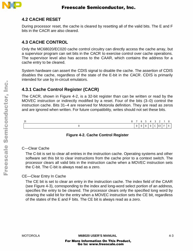
MOTOROLA M68020 USER’S MANUAL 4-3
4.2 CACHE RESET
During processor reset, the cache is cleared by resetting all of the valid bits. The E and Fbits in the CACR are also cleared.
4.3 CACHE CONTROL
Only the MC68020/EC020 cache control circuitry can directly access the cache array, buta supervisor program can set bits in the CACR to exercise control over cache operations.The supervisor level also has access to the CAAR, which contains the address for acache entry to be cleared.
System hardware can assert the CDIS signal to disable the cache. The assertion of CDISdisables the cache, regardless of the state of the E-bit in the CACR. CDIS is primarilyintended for use by in-circuit emulators.
4.3.1 Cache Control Register (CACR)
The CACR, shown in Figure 4-2, is a 32-bit register than can be written or read by theMOVEC instruction or indirectly modified by a reset. Four of the bits (3–0) control theinstruction cache. Bits 31–4 are reserved for Motorola definition. They are read as zerosand are ignored when written. For future compatibility, writes should not set these bits.
031
E
1
F
2
CE
3
C
4
0
5
0
6
0
7
0
8
0
Figure 4-2. Cache Control Register
C—Clear CacheThe C-bit is set to clear all entries in the instruction cache. Operating systems and othersoftware set this bit to clear instructions from the cache prior to a context switch. Theprocessor clears all valid bits in the instruction cache when a MOVEC instruction setsthe C-bit. The C-bit is always read as a zero.
CE—Clear Entry In CacheThe CE bit is set to clear an entry in the instruction cache. The index field of the CAAR(see Figure 4-3), corresponding to the index and long-word select portion of an address,specifies the entry to be cleared. The processor clears only the specified long word byclearing the valid bit for the entry when a MOVEC instruction sets the CE bit, regardlessof the states of the E and F bits. The CE bit is always read as a zero.
Fre
esc
ale
Se
mic
on
du
cto
r, I
Freescale Semiconductor, Inc.
For More Information On This Product, Go to: www.freescale.com
nc
...

4–4 M68020 USER’S MANUAL MOTOROLA
F—Freeze CacheThe F-bit is set to freeze the instruction cache. When the F-bit is set and a cache missoccurs, the entry (or line) is not replaced. When the F-bit is clear, a cache miss causesthe entry (or line) to be filled. A reset operation clears the F-bit.
E—Enable CacheThe E-bit is set to enable the instruction cache. When it is clear, the instruction cache isdisabled. A reset operation clears the E-bit. The supervisor normally enables theinstruction cache, but it can clear the E-bit for system debugging or emulation, asrequired. Disabling the instruction cache does not flush the entries. If the cache isreenabled, the previously valid entries remain valid and may be used.
4.3.2 Cache Address Register (CAAR)
The format of the 32-bit CAAR is shown in Figure 4-3.
031
RESERVED
12
INDEX
78
RESERVED
Figure 4-3. Cache Address Register
Bits 31–8, 1, and 0—ReservedThese bits are reserved for use by Motorola.
Index FieldThe index field contains the address for the “clear cache entry” operations. The bits ofthis field, which correspond to A7–A2, specify the index and a long word of a cache line.
Fre
esc
ale
Se
mic
on
du
cto
r, I
Freescale Semiconductor, Inc.
For More Information On This Product, Go to: www.freescale.com
nc
...

MOTOROLA M68020 USER’S MANUAL 5-1
SECTION 5BUS OPERATION
This section provides a functional description of the bus, the signals that control it, and thebus cycles provided for data transfer operations. It also describes the error and haltconditions, bus arbitration, and reset operation. Operation of the bus is the same whetherthe processor or an external device is the bus master; the names and descriptions of buscycles are from the point of view of the bus master. For exact timing specifications, refer toSection 10 Electrical Characteristics .
The MC68020/EC020 architecture supports byte, word, and long-word operands, allowingaccess to 8-, 16-, and 32-bit data ports through the use of asynchronous cycles controlledby the DSACK1 and DSACK0 input signals.
The MC68020/EC020 allows byte, word, and long-word operands to be located in memoryon any byte boundary. For a misaligned transfer, more than one bus cycle may berequired to complete the transfer, regardless of port size. For a port less than 32 bits wide,multiple bus cycles may be required for an operand transfer due to either misalignment ora port width smaller than the operand size. Instruction words and their associatedextension words must be aligned on word boundaries. The user should be aware thatmisalignment of word or long-word operands can cause the MC68020/EC020 to performmultiple bus cycles for the operand transfer; therefore, processor performance isoptimized if word and long-word memory operands are aligned on word or long-wordboundaries, respectively.
5.1 BUS TRANSFER SIGNALS
The bus transfers information between the MC68020/EC020 and an external memory,coprocessor, or peripheral device. External devices can accept or provide 8 bits, 16 bits,or 32 bits in parallel and must follow the handshake protocol described in this section. Themaximum number of bits accepted or provided during a bus transfer is defined as the portwidth. The MC68020/EC020 contains an address bus that specifies the address for thetransfer and a data bus that transfers the data. Control signals indicate the beginning ofthe cycle, the address space and size of the transfer, and the type of cycle. The selecteddevice then controls the length of the cycle with the signal(s) used to terminate the cycle.Strobe signals, one for the address bus and another for the data bus, indicate the validityof the address and provide timing information for the data.
The bus operates in an asynchronous mode for any port width. The bus and control inputsignals are internally synchronized to the MC68020/EC020 clock, introducing a delay. Thisdelay is the time period required for the MC68020/EC020 to sample an input signal,synchronize the input to the internal clocks of the processor, and determine whether the
Fre
esc
ale
Se
mic
on
du
cto
r, I
Freescale Semiconductor, Inc.
For More Information On This Product, Go to: www.freescale.com
nc
...
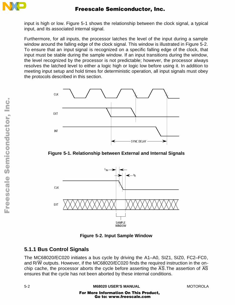
5-2 M68020 USER’S MANUAL MOTOROLA
input is high or low. Figure 5-1 shows the relationship between the clock signal, a typicalinput, and its associated internal signal.
Furthermore, for all inputs, the processor latches the level of the input during a samplewindow around the falling edge of the clock signal. This window is illustrated in Figure 5-2.To ensure that an input signal is recognized on a specific falling edge of the clock, thatinput must be stable during the sample window. If an input transitions during the window,the level recognized by the processor is not predictable; however, the processor alwaysresolves the latched level to either a logic high or logic low before using it. In addition tomeeting input setup and hold times for deterministic operation, all input signals must obeythe protocols described in this section.
SYNC DELAY
CLK
EXT
INT
Figure 5-1. Relationship between External and Internal Signals
t su
th
SAMPLEWINDOW
CLK
EXT
Figure 5-2. Input Sample Window
5.1.1 Bus Control Signals
The MC68020/EC020 initiates a bus cycle by driving the A1–A0, SIZ1, SIZ0, FC2–FC0,and R/W outputs. However, if the MC68020/EC020 finds the required instruction in the on-chip cache, the processor aborts the cycle before asserting the AS.The assertion of AS
ensures that the cycle has not been aborted by these internal conditions.
Fre
esc
ale
Se
mic
on
du
cto
r, I
Freescale Semiconductor, Inc.
For More Information On This Product, Go to: www.freescale.com
nc
...

MOTOROLA M68020 USER’S MANUAL 5-3
When initiating a bus cycle, the MC68020 asserts ECS in addition to A1–A0, SIZ1, SIZ0,FC2–FC0, and R/W . ECS can be used to initiate various timing sequences that areeventually qualified with AS. Qualification with AS may be required since, in the case of aninternal cache hit, a bus cycle may be aborted after ECS has been asserted. During thefirst MC68020 external bus cycle of an operand transfer, OCS is asserted with ECS. Whenseveral bus cycles are required to transfer the entire operand, OCS is asserted only at thebeginning of the first external bus cycle. With respect to OCS , an “operand” is any entityrequired by the execution unit, whether a program or data item. Note that ECS and OCS
are not implemented in the MC68EC020.
The FC2–FC0 signals select one of eight address spaces (see Table 2-1) to which theaddress applies. Five address spaces are presently defined. Of the remaining three, oneis reserved for user definition, and two are reserved by Motorola for future use. FC2–FC0are valid while AS is asserted.
The SIZ1 and SIZ0 signals indicate the number of bytes remaining to be transferredduring an operand cycle (consisting of one or more bus cycles) or during a cache filloperation from a device with a port size that is less than 32 bits. Table 5-2 lists theencoding of SIZ1 and SIZ0. SIZ1 and SIZ0 are valid while AS is asserted.
The R/W signal determines the direction of the transfer during a bus cycle. When required,this signal changes state at the beginning of a bus cycle and is valid while AS is asserted.R/W only transitions when a write cycle is preceded by a read cycle or vice versa. Thissignal may remain low for two consecutive write cycles.
The RMC signal is asserted at the beginning of the first bus cycle of a read-modify-writeoperation and remains asserted until completion of the final bus cycle of the operation.The RMC signal is guaranteed to be negated before the end of state 0 for a bus cyclefollowing a read-modify-write operation.
5.1.2 Address Bus
A31–A0 (for the MC68020) or A23–A0 (for the MC68EC020) define the address of thebyte (or the most significant byte) to be transferred during a bus cycle. The processorplaces the address on the bus at the beginning of a bus cycle. The address is valid whileAS is asserted. In the MC68EC020, A31–A24 are used internally, but not externally.
5.1.3 Address Strobe
AS is a timing signal that indicates the validity of an address on the address bus and ofmany control signals. It is asserted one-half clock after the beginning of a bus cycle.
5.1.4 Data Bus
D31–D0 comprise a bidirectional, nonmultiplexed parallel bus that contains the data beingtransferred to or from the processor. A read or write operation may transfer 8, 16, 24, or32 bits of data (one, two, three, or four bytes) in one bus cycle. During a read cycle, thedata is latched by the processor on the last falling edge of the clock for that bus cycle. For
Fre
esc
ale
Se
mic
on
du
cto
r, I
Freescale Semiconductor, Inc.
For More Information On This Product, Go to: www.freescale.com
nc
...

5-4 M68020 USER’S MANUAL MOTOROLA
a write cycle, all 32 bits of the data bus are driven, regardless of the port width or operandsize. The processor places the data on the data bus one-half clock cycle after AS isasserted in a write cycle.
5.1.5 Data Strobe
DS is a timing signal that applies to the data bus. For a read cycle, the processor assertsDS to signal the external device to place data on the bus. DS is asserted at the same timeas AS during a read cycle. For a write cycle, DS notifies the external device that the datato be written is valid. The processor asserts DS one full clock cycle after the assertion ofAS during a write cycle.
5.1.6 Data Buffer Enable
The MC68020 DBEN signal is used to enable external data buffers while data is presenton the data bus. During a read operation, DBEN is asserted one clock cycle after thebeginning of the bus cycle and is negated as DS is negated. In a write operation, DBEN isasserted at the time AS is asserted and is held active for the duration of the cycle. Notethat DBEN is implemented in the MC68020 and is not implemented in the MC68EC020.
5.1.7 Bus Cycle Termination Signals
During bus cycles, external devices assert DSACK1/DSACK0 as part of the bus protocol.During a read cycle, DSACK1/DSACK0 assertion signals the processor to terminate thebus cycle and to latch the data. During a write cycle, the assertion of DSACK1/DSACK0
indicates that the external device has successfully stored the data and that the cycle mayterminate. DSACK1/DSACK0 also indicate to the processor the size of the port for the buscycle just completed, as shown in Table 5-1. Refer to 5.3.1 Read Cycle for timingrelationships of DSACK1/DSACK0.
The BERR signal is also a bus cycle termination indicator and can be used in the absenceof DSACK1/DSACK0 to indicate a bus error condition. It can also be asserted inconjunction with DSACK1/DSACK0 to indicate a bus error condition, provided it meets theappropriate timing described in this section and in Section 10 Electrical Characteristics.Additionally, the BERR and HALT signals can be asserted together to indicate a retrytermination. Again, the BERR and HALT signals can be simultaneously asserted in lieu of,or in conjunction with, the DSACK1/DSACK0 signals.
Finally, the AVEC signal can be used to terminate interrupt acknowledge cycles, indicatingthat the MC68020/EC020 should generate a vector number to locate an interrupt handlerroutine. AVEC is ignored during all other bus cycles.
Fre
esc
ale
Se
mic
on
du
cto
r, I
Freescale Semiconductor, Inc.
For More Information On This Product, Go to: www.freescale.com
nc
...
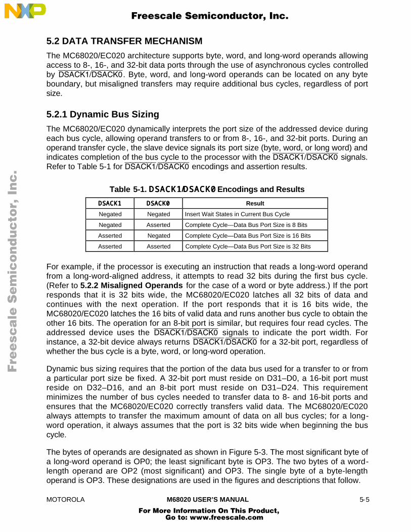
MOTOROLA M68020 USER’S MANUAL 5-5
5.2 DATA TRANSFER MECHANISM
The MC68020/EC020 architecture supports byte, word, and long-word operands allowingaccess to 8-, 16-, and 32-bit data ports through the use of asynchronous cycles controlledby DSACK1/DSACK0 . Byte, word, and long-word operands can be located on any byteboundary, but misaligned transfers may require additional bus cycles, regardless of portsize.
5.2.1 Dynamic Bus Sizing
The MC68020/EC020 dynamically interprets the port size of the addressed device duringeach bus cycle, allowing operand transfers to or from 8-, 16-, and 32-bit ports. During anoperand transfer cycle, the slave device signals its port size (byte, word, or long word) andindicates completion of the bus cycle to the processor with the DSACK1/DSACK0 signals.Refer to Table 5-1 for DSACK1/DSACK0 encodings and assertion results.
Table 5-1. DSACK1/DSACK0 Encodings and Results
DSACK1 DSACK0 Result
Negated Negated Insert Wait States in Current Bus Cycle
Negated Asserted Complete Cycle—Data Bus Port Size is 8 Bits
Asserted Negated Complete Cycle—Data Bus Port Size is 16 Bits
Asserted Asserted Complete Cycle—Data Bus Port Size is 32 Bits
For example, if the processor is executing an instruction that reads a long-word operandfrom a long-word-aligned address, it attempts to read 32 bits during the first bus cycle.(Refer to 5.2.2 Misaligned Operands for the case of a word or byte address.) If the portresponds that it is 32 bits wide, the MC68020/EC020 latches all 32 bits of data andcontinues with the next operation. If the port responds that it is 16 bits wide, theMC68020/EC020 latches the 16 bits of valid data and runs another bus cycle to obtain theother 16 bits. The operation for an 8-bit port is similar, but requires four read cycles. Theaddressed device uses the DSACK1/DSACK0 signals to indicate the port width. Forinstance, a 32-bit device always returns DSACK1/DSACK0 for a 32-bit port, regardless ofwhether the bus cycle is a byte, word, or long-word operation.
Dynamic bus sizing requires that the portion of the data bus used for a transfer to or froma particular port size be fixed. A 32-bit port must reside on D31–D0, a 16-bit port mustreside on D32–D16, and an 8-bit port must reside on D31–D24. This requirementminimizes the number of bus cycles needed to transfer data to 8- and 16-bit ports andensures that the MC68020/EC020 correctly transfers valid data. The MC68020/EC020always attempts to transfer the maximum amount of data on all bus cycles; for a long-word operation, it always assumes that the port is 32 bits wide when beginning the buscycle.
The bytes of operands are designated as shown in Figure 5-3. The most significant byte ofa long-word operand is OP0; the least significant byte is OP3. The two bytes of a word-length operand are OP2 (most significant) and OP3. The single byte of a byte-lengthoperand is OP3. These designations are used in the figures and descriptions that follow.
Fre
esc
ale
Se
mic
on
du
cto
r, I
Freescale Semiconductor, Inc.
For More Information On This Product, Go to: www.freescale.com
nc
...

5-6 M68020 USER’S MANUAL MOTOROLA
OP0 OP1 OP2 OP3
31 0
15 0
OP2 OP3
7 0
LONG-WORD OPERAND
WORD OPERAND
BYTE OPERAND OP3
Figure 5-3. Internal Operand Representation
Figure 5-4 shows the required organization of data ports on the MC68020/EC020 bus for8-, 16-, and 32-bit devices. The four bytes shown in Figure 5-4 are connected through theinternal data bus and data multiplexer to the external data bus. This path is the meansthrough which the MC68020/EC020 supports dynamic bus sizing and operandmisalignment. Refer to 5.2.2 Misaligned Operands for the definition of misalignedoperand. The data multiplexer establishes the necessary connections for differentcombinations of address and data sizes.
0 1 2 3
ROUTING AND DUPLICATION
BYTE 0
BYTE 2
BYTE 1
BYTE 316-BIT PORT
REGISTER
MULTIPLEXER
EXTERNAL DATA BUS
ADDRESSxxxxxxx0
xxxxxxx0
2
INCREASINGMEMORY
ADDRESSES
D31– D24 D23–D16 D15–D8 D7–D0
BYTE 0 BYTE 1 BYTE 2 BYTE 3
BYTE 0
BYTE 1
BYTE 2
BYTE 3
8-BIT PORT2
3
1
xxxxxxx0
EXTERNAL BUS
INTERNAL TOTHE MC68020/EC020
32-BIT PORT
OP0 OP1 OP2 OP3
Figure 5-4. MC68020/EC020 Interface to Various Port Sizes
Fre
esc
ale
Se
mic
on
du
cto
r, I
Freescale Semiconductor, Inc.
For More Information On This Product, Go to: www.freescale.com
nc
...

MOTOROLA M68020 USER’S MANUAL 5-7
The multiplexer takes the four bytes of the 32-bit bus and routes them to their requiredpositions. For example, OP0 can be routed to D31–D24, as would be the normal case, orit can be routed to any other byte position to support a misaligned transfer. The same istrue for any of the operand bytes. The positioning of bytes is determined by the SIZ1,SIZ0, A1, and A0 outputs.
The SIZ1 and SIZ0 outputs indicate the remaining number of bytes to be transferredduring the current bus cycle, as listed in Table 5-2.
Table 5-2. SIZ1, SIZ0 Signal Encoding
SIZ1 SIZ0 Size
Negated Asserted Byte
Asserted Negated Word
Asserted Asserted 3 Bytes
Negated Negated Long Word
The number of bytes transferred during a write or read bus cycle is equal to or less thanthe size indicated by the SIZ1 and SIZ0 outputs, depending on port width and operandalignment. For example, during the first bus cycle of a long-word transfer to a word port,the SIZ1 and SIZ0 outputs indicate that four bytes are to be transferred, although only twobytes are moved on that bus cycle.
A1–A0 also affect operation of the data multiplexer. During an operand transfer, A31–A2(for the MC68020) or A23–A2 (for the MC68EC020) indicate the long-word base addressof that portion of the operand to be accessed; A1 and A0 indicate the byte offset from thebase. Table 5-3 lists the encodings of A1 and A0 and the corresponding byte offsets fromthe long-word base.
Table 5-3. Address Offset Encodings
A1 A0 Offset
Negated Negated +0 Bytes
Negated Asserted +1 Byte
Asserted Negated +2 Bytes
Asserted Asserted +3 Bytes
Fre
esc
ale
Se
mic
on
du
cto
r, I
Freescale Semiconductor, Inc.
For More Information On This Product, Go to: www.freescale.com
nc
...
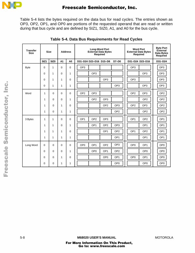
5-8 M68020 USER’S MANUAL MOTOROLA
Table 5-4 lists the bytes required on the data bus for read cycles. The entries shown asOP3, OP2, OP1, and OP0 are portions of the requested operand that are read or writtenduring that bus cycle and are defined by SIZ1, SIZ0, A1, and A0 for the bus cycle.
Table 5-4. Data Bus Requirements for Read Cycles
Byte PortExternal
Data BytesRequired
Word PortExternal Data Bytes
Required
Long-Word PortExternal Data Bytes
RequiredAddressSizeTransfer
Size
SIZ1 SIZ0 A1 A0
OP3 OP3
OP3
OP3
OP3 OP3
OP3
OP3
OP3
D31–D24D23–D16D31–D24D23–D16D31–D24 D7–D0D15–D8
OP3
OP3
OP3
Byte 0
1
1
1
1 0 0
0
0
0
1
1
0 1
0
1
OP2 OP2
OP2
OP2
OP2 OP2
OP2
OP2
OP2
OP2
OP2
OP2
Word 1
0
1
1
0 0 0
1
1
1
0
0
0 1
0
1
OP1 OP1
OP1
OP1
OP1 OP1
OP1
OP1
OP1
OP1
OP1
OP1
3 Bytes 1
1
1
1
1 0 0
1
1
1
1
1
0 1
0
1
OP0 OP0
OP0
OP0
OP0 OP0
OP0
OP0
OP0
OP0
OP0
OP0
Long Word 0
0
1
1
0 0 0
0
0
0
0
0
0 1
0
1
OP3
OP3
OP2
OP2
OP1
OP1
OP1
OP1
OP2
OP1
OP2
OP3
OP2
OP3OP2
OP3OP2
OP3
OP3
OP3
Fre
esc
ale
Se
mic
on
du
cto
r, I
Freescale Semiconductor, Inc.
For More Information On This Product, Go to: www.freescale.com
nc
...
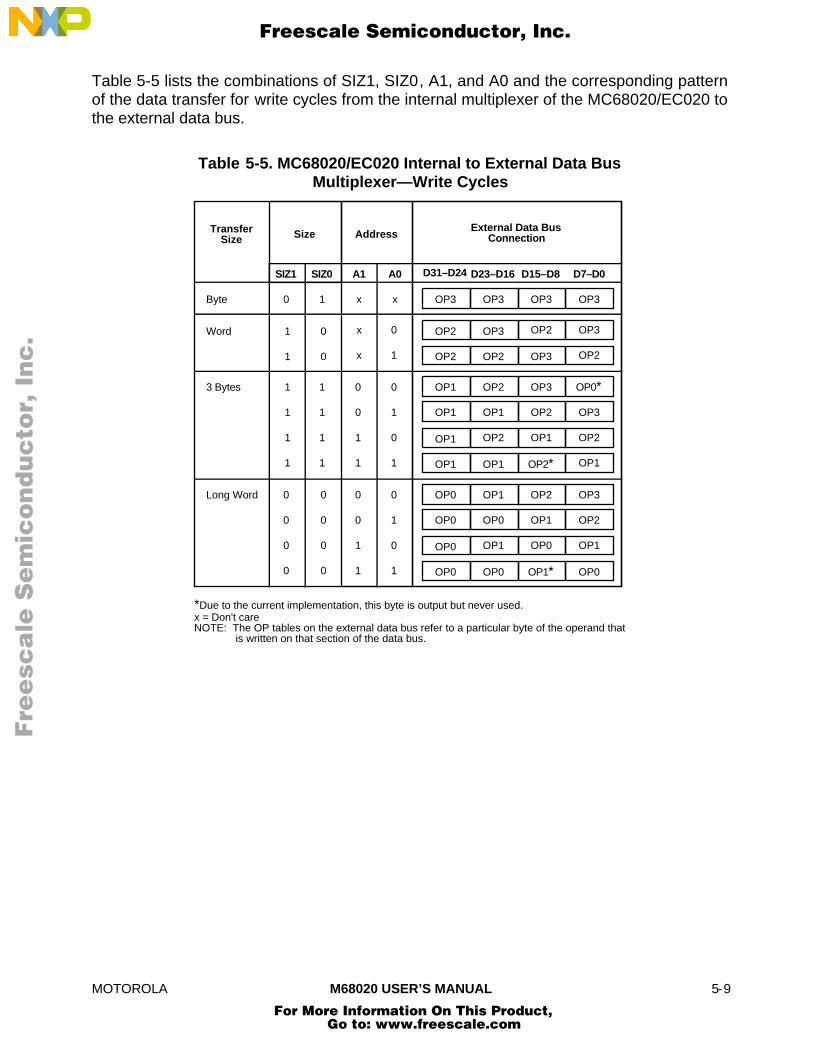
MOTOROLA M68020 USER’S MANUAL 5-9
Table 5-5 lists the combinations of SIZ1, SIZ0, A1, and A0 and the corresponding patternof the data transfer for write cycles from the internal multiplexer of the MC68020/EC020 tothe external data bus.
Table 5-5. MC68020/EC020 Internal to External Data BusMultiplexer—Write Cycles
OP0*
External Data BusConnectionAddressSizeTransfer
Size
SIZ1 SIZ0 A1 A0
OP3
D23–D16D31–D24 D7–D0D15–D8
Byte 0 1 x x
OP2
OP2
Word 1
0
0 x 0
1 x 1
OP1
OP1
OP1
OP1
3 Bytes 1
1
1
1
1 0 0
1
1
1
1
1
0 1
0
1
OP0
OP0
OP0
OP0
Long Word 0
0
1
1
0 0 0
0
0
0
0
0
0 1
0
1
OP1
OP1
OP2
OP1
OP2
OP3
OP2
OP3OP2
OP3OP2
OP3
OP3
OP3
OP2
OP3
OP2
OP3
OP3
OP1
OP1
OP1
OP2
OP1
OP0
OP0
OP0
OP1
OP0 OP1*
OP2
OP2*
*Due to the current implementation, this byte is output but never used.x = Don't careNOTE: The OP tables on the external data bus refer to a particular byte of the operand thatis written on that section of the data bus.
Fre
esc
ale
Se
mic
on
du
cto
r, I
Freescale Semiconductor, Inc.
For More Information On This Product, Go to: www.freescale.com
nc
...

5-10 M68020 USER’S MANUAL MOTOROLA
Figure 5-5 shows the transfer (write) of a long-word operand to a word port. In the first buscycle, the MC68020/EC020 places the four operand bytes on the external bus. Since theaddress is long-word aligned in this example, the multiplexer follows the pattern in theentry of Table 5-5 corresponding to SIZ0, SIZ1, A0, A1 = 0000. The port latches the dataon D31–D16, asserts DSACK1 (DSACK0 remains negated), and the processor terminatesthe bus cycle. It then starts a new bus cycle with SIZ1, SIZ0, A1, A0 = 1010 to transfer theremaining 16 bits. SIZ1 and SIZ0 indicate that a word remains to be transferred; A1 andA0 indicate that the word corresponds to an offset of two from the base address. Themultiplexer follows the pattern corresponding to this configuration of SIZ1, SIZ0, A1, andA0 and places the two least significant bytes of the long word on the word portion of thebus (D31–D16). The bus cycle transfers the remaining bytes to the word-sized port. Figure5-6 shows the timing of the bus transfer signals for this operation.
DATA BUSD31 D16
LONG-WORD OPERAND
OP0 OP1 OP2 OP3
31 0
WORD MEMORY
MSB LSB
OP0 OP1
OP2 OP3
MC68020/EC020
SIZ1 SIZ0 A1 A0
0 0 0 0
1 0 1 0
MEMORY CONTROL
DSACK1 DSACK0
L H
L H
Figure 5-5. Long-Word Operand Write to Word Port Example
Fre
esc
ale
Se
mic
on
du
cto
r, I
Freescale Semiconductor, Inc.
For More Information On This Product, Go to: www.freescale.com
nc
...
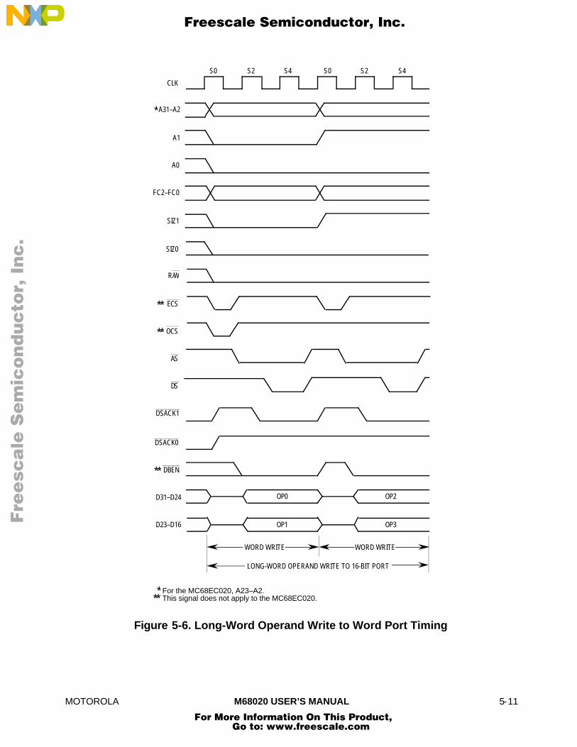
MOTOROLA M68020 USER’S MANUAL 5-11
WORD WRITE
LONG-WORD OPERAND WRITE TO 16-BIT PORT
S0 S2 S4 S0 S2 S4
CLK
A31–A2
A1
A0
FC2–FC0
SIZ1
SIZ0
R/W
ECS
OCS
AS
DS
DSACK1
DSACK0
DBEN
D31–D24
D23–D16
WORD WRITE
OP0
OP1
OP2
OP3
**
**
**
*
* For the MC68EC020, A23–A2.This signal does not apply to the MC68EC020.**
Figure 5-6. Long-Word Operand Write to Word Port Timing
Fre
esc
ale
Se
mic
on
du
cto
r, I
Freescale Semiconductor, Inc.
For More Information On This Product, Go to: www.freescale.com
nc
...

5-12 M68020 USER’S MANUAL MOTOROLA
Figure 5-7 shows a word write to an 8-bit bus port. Like the preceding example, thisexample requires two bus cycles. Each bus cycle transfers a single byte. SIZ1 and SIZ0for the first cycle specify two bytes; for the second cycle, one byte. Figure 5-8 shows theassociated bus transfer signal timing.
OP2 OP3
15 0WORD OPERAND
D31 DATA BUS D24
BYTE MEMORY
OP2
OP3
MC68020/EC020
SIZ1 SIZ0 A1 A01 0 0 0
0 1 0 1
MEMORY CONTROL
DSACK1 DSACK0H L
H L
Figure 5-7. Word Operand Write to Byte Port Example
Fre
esc
ale
Se
mic
on
du
cto
r, I
Freescale Semiconductor, Inc.
For More Information On This Product, Go to: www.freescale.com
nc
...
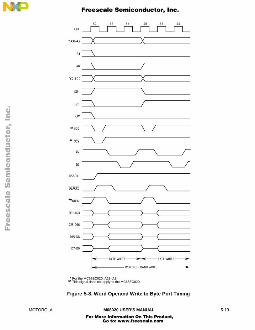
MOTOROLA M68020 USER’S MANUAL 5-13
BYTE WRITE
WORD OPERAND WRITE
S0 S2 S4 S0 S2 S4
CLK
A31–A2
A1
A0
FC2–FC0
SIZ1
SIZ0
R/W
ECS
OCS
AS
DS
DSACK1
DSACK0
DBEN
D31–D24
D23–D16
BYTE WRITE
D15–D8
D7–D0
**
**
**
*
* For the MC68EC020, A23–A2.This signal does not apply to the MC68EC020.**
Figure 5-8. Word Operand Write to Byte Port Timing
Fre
esc
ale
Se
mic
on
du
cto
r, I
Freescale Semiconductor, Inc.
For More Information On This Product, Go to: www.freescale.com
nc
...

5-14 M68020 USER’S MANUAL MOTOROLA
5.2.2 Misaligned Operands
Since operands may reside at any byte boundary, they may be misaligned. A byteoperand is properly aligned at any address; a word operand is misaligned at an oddaddress; a long word is misaligned at an address that is not evenly divisible by four. TheMC68000, MC68008, and MC68010 implementations allow long-word transfers on odd-word boundaries but force exceptions if word or long-word operand transfers areattempted at odd-byte addresses. Although the MC68020/EC020 does not enforce anyalignment restrictions for data operands (including PC relative data addresses), someperformance degradation occurs when additional bus cycles are required for long-word orword operands that are misaligned. For maximum performance, data items should bealigned on their natural boundaries. All instruction words and extension words must resideon word boundaries. Attempting to prefetch an instruction word at an odd address causesan address error exception.
Figure 5-9 shows the transfer (write) of a long-word operand to an odd address in word-organized memory, which requires three bus cycles. For the first cycle, SIZ1 and SIZ0specify a long-word transfer, and A2–A0 = 001. Since the port width is 16 bits, only thefirst byte of the long word is transferred. The slave device latches the byte andacknowledges the data transfer, indicating that the port is 16 bits wide. When theprocessor starts the second cycle, SIZ1 and SIZ0 specify that three bytes remain to betransferred with A2–A0 = 010. The next two bytes are transferred during this cycle. Theprocessor then initiates the third cycle, with SIZ1 and SIZ0 indicating one byte remainingto be transferred with A2–A0 = 100. The port latches the final byte, and the operation iscomplete. Figure 5-10 shows the associated bus transfer signal timing. Figure 5-11 showsthe equivalent operation for a data read cycle.
DATA BUSD31 D16
LONG-WORD OPERAND
OP0 OP1 OP2 OP3
31 0
WORD MEMORY
MSB LSB
XXX OP0
OP1 OP2
MC68020/EC020
SIZ1 SIZ0 A2 A1
0 0 0 0
1 1 0 1
MEMORY CONTROL
DSACK1 DSACK0
L H
L H
OP3 XXX
A0
1
0
0 1 1 0 0 L H
Figure 5-9. Misaligned Long-Word Operand Write to Word Port Example
Fre
esc
ale
Se
mic
on
du
cto
r, I
Freescale Semiconductor, Inc.
For More Information On This Product, Go to: www.freescale.com
nc
...

MOTOROLA M68020 USER’S MANUAL 5-15
BYTE WRITE
LONG-WORD OPERAND WRITE
S0 S2 S4 S0 S2 S4
CLK
A31–A2
A1
A0
FC2–FC0
SIZ1
SIZ0
R/W
ECS
OCS
AS
DS
DSACK1
DSACK0
DBEN
D31–D24
D23–D16
WORD WRITE
D15–D8
D7–D0
S0 S2 S4
OP0
OP0
OP1
OP2
OP1
OP2
OP1
OP2
OP3
OP3
OP3
OP3
BYTE WRITE
**
**
**
*
* For the MC68EC020, A23–A2.This signal does not apply to the MC68EC020.
Figure 5-10. Misaligned Long-Word Operand Write to Word Port Timing
Fre
esc
ale
Se
mic
on
du
cto
r, I
Freescale Semiconductor, Inc.
For More Information On This Product, Go to: www.freescale.com
nc
...

5-16 M68020 USER’S MANUAL MOTOROLA
OP0 OP1 OP2 OP3
31 0LONG-WORD OPERAND (REGISTER)
DATA BUSD31 D16
WORD MEMORY
MSB LSB
XXX OP0
OP1 OP2
OP3 XXX
MC68020/EC020
SIZ1 SIZ0 A2 A1
0 0 0 0 1
1 1 0 1 0
0 1 1 0 0
A0
MEMORY CONTROL
DSACK1 DSACK0
L H
L H
L H
Figure 5-11. Misaligned Long-Word Operand Readfrom Word Port Example
Figures 5-12 and 5-13 show a word transfer (write) to an odd address in word-organizedmemory. This example is similar to the one shown in Figures 5-9 and 5-10 except that theoperand is word sized and the transfer requires only two bus cycles. Figure 5-14 showsthe equivalent operation for a data read cycle.
MC68020/EC020
SIZ1 SIZ0 A2 A1
1 0 0 0 1
0 1 0 1 0
A0
MEMORY CONTROL
DSACK1 DSACK0
L H
L H
OP2 OP3
15 0WORD OPERAND
DATA BUSD31 D16
WORD MEMORY
MSB LSB
XXX
OP3
OP2
XXX
Figure 5-12. Misaligned Word Operand Write to Word Port Example
Fre
esc
ale
Se
mic
on
du
cto
r, I
Freescale Semiconductor, Inc.
For More Information On This Product, Go to: www.freescale.com
nc
...
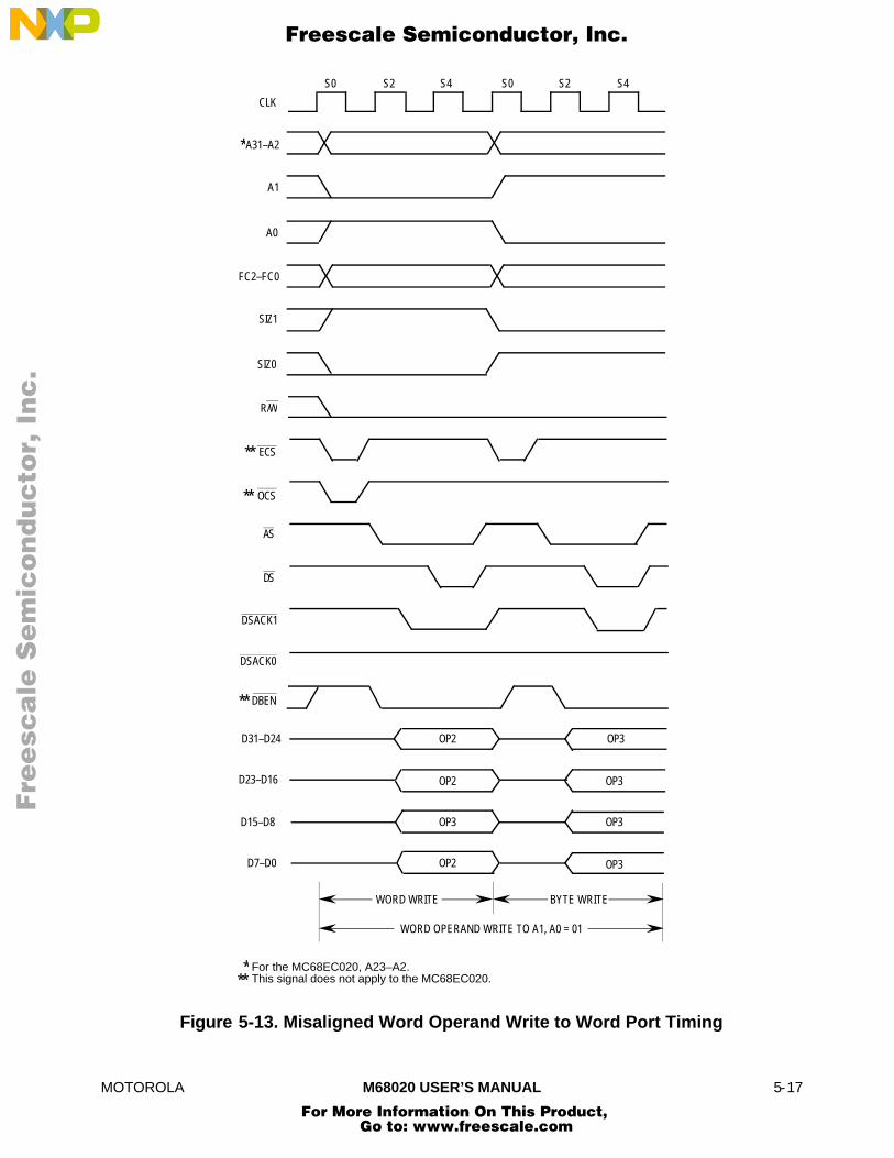
MOTOROLA M68020 USER’S MANUAL 5-17
WORD OPERAND WRITE TO A1, A0 = 01
S0 S2 S4 S0 S2 S4
CLK
A31–A2
A1
A0
FC2–FC0
SIZ1
SIZ0
R/W
ECS
OCS
AS
DS
DSACK1
DSACK0
DBEN
D31–D24
D23–D16
WORD WRITE
D15–D8
D7–D0
OP2
OP2
OP3
OP2
OP3
OP3
OP3
OP3
BYTE WRITE
**
**
**
*
* For the MC68EC020, A23–A2.This signal does not apply to the MC68EC020.**
Figure 5-13. Misaligned Word Operand Write to Word Port Timing
Fre
esc
ale
Se
mic
on
du
cto
r, I
Freescale Semiconductor, Inc.
For More Information On This Product, Go to: www.freescale.com
nc
...

5-18 M68020 USER’S MANUAL MOTOROLA
MC68020/EC020
SIZ1 SIZ0 A2 A1
1 0 0 0 1
0 1 0 1 0
A0
MEMORY CONTROL
DSACK1 DSACK0
L H
L H
OP2 OP3
15 0WORD OPERAND (REGISTER)
DATA BUSD31 D16
WORD MEMORY
MSB LSB
XXX
OP3
OP2
XXX
Figure 5-14. Misaligned Word Operand Read from Word Bus Example
Figures 5-15 and 5-16 show an example of a long-word transfer (write) to an odd addressin long-word-organized memory. In this example, a long-word access is attemptedbeginning at the least significant byte of a long-word-organized memory. Only one bytecan be transferred in the first bus cycle. The second bus cycle then consists of a three-byte access to a long-word boundary. Since the memory is long word organized, nofurther bus cycles are necessary. Figure 5-17 shows the equivalent operation for a dataread cycle.
MC68020/EC020
SIZ1 SIZ0 A2 A1
0 0 0 1 1
1 1 1 0 0
A0
MEMORY CONTROL
DSACK1 DSACK0
L
L L
OP0 OP1
31 0LONG-WORD OPERAND
DATA BUSD31 D0
LONG-WORD MEMORY
MSB UMB
XXX
OP1 OP2
XXX
OP2 OP3
XXX
OP3
OP0
XXX
LMB LSB
L
Figure 5-15. Misaligned Long-Word Operand Writeto Long-Word Port Example
Fre
esc
ale
Se
mic
on
du
cto
r, I
Freescale Semiconductor, Inc.
For More Information On This Product, Go to: www.freescale.com
nc
...

MOTOROLA M68020 USER’S MANUAL 5-19
LONG-WORD OPERAND WRITE
S0 S2 S4 S0 S2 S4
CLK
A31–A2
A1
A0
FC2–FC0
SIZ1
SIZ0
R/W
ECS
OCS
AS
DS
DSACK1
DSACK0
DBEN
D31–D24
D23–D16
BYTE WRITE
D15–D8
D7–D0
OP0
OP0
OP1
OP0
OP1
OP2
OP3
OP1
3-BYTE WRITE
**
**
**
*
* For the MC68EC020, A23–A2.This signal does not apply to the MC68EC020.**
Figure 5-16. Misaligned Long-Word Operand Writeto Long-Word Port Timing
Fre
esc
ale
Se
mic
on
du
cto
r, I
Freescale Semiconductor, Inc.
For More Information On This Product, Go to: www.freescale.com
nc
...

5-20 M68020 USER’S MANUAL MOTOROLA
MC68020/EC020
SIZ1 SIZ0 A2 A1
0 0 0 1 1
1 1 1 0 0
A0
MEMORY CONTROL
DSACK1 DSACK0
L
L L
OP0 OP1
31 0LONG-WORD OPERAND (REGISTER)
DATA BUSD31 D0
LONG-WORD MEMORY
MSB UMB
XXX
OP1 OP2
XXX
OP2 OP3
XXX
OP3
OP0
XXX
LMB LSB
L
Figure 5-17. Misaligned Long-Word Operand Readfrom Long-Word Port Example
5.2.3 Effects of Dynamic Bus Sizing and Operand Misalignment
The combination of operand size, operand alignment, and port size determine the numberof bus cycles required to perform a particular memory access. Table 5-6 lists the numberof bus cycles required for different operand sizes to different port sizes with all possiblealignment conditions for read/write cycles.
Table 5-6. Memory Alignment and Port SizeInfluence on Read/Write Bus Cycles
Number of Bus Cycles(Data Port Size = 32 Bits:16 Bits:8 Bits)
A1, A0
Operand Size 00 01 10 11
Instruction* 1:2:4 N/A N/A N/A
Byte Operand 1:1:1 1:1:1 1:1:1 1:1:1
Word Operand 1:1:2 1:2:2 1:1:2 2:2:2
Long-Word Operand 1:2:4 2:3:4 2:2:4 2:3:4
*Instruction prefetches are always two words from a long-word boundary
Table 5-6 reveals that bus cycle throughput is significantly affected by port size andalignment. The MC68020/EC020 system designer and programmer should be aware ofand account for these effects, particularly in time-critical applications.
Fre
esc
ale
Se
mic
on
du
cto
r, I
Freescale Semiconductor, Inc.
For More Information On This Product, Go to: www.freescale.com
nc
...
MOTOROLA M68020 USER’S MANUAL 5-21
Table 5-6 demonstrates that the processor always prefetches instructions by reading along word from a long-word address (A1, A0 = 00), regardless of port size or alignment.When the required instruction begins at an odd-word boundary, the processor attempts tofetch the entire 32 bits and loads both words into the instruction cache, if possible,although the second one is the required word. Even if the instruction access is not cached,the entire 32 bits are latched into an internal cache holding register from which the twoinstructions words can subsequently be referenced. Refer to Section 8 InstructionExecution Timing for a complete description of the cache holding register and pipelineoperation.
5.2.4 Address, Size, and Data Bus Relationships
The data transfer examples show how the MC68020/EC020 drives data onto or receivesdata from the correct byte sections of the data bus. Table 5-7 shows the combinations ofthe SIZ1, SIZ0, A1, and A0 signals that can be used to generate byte enable signals foreach of the four sections of the data bus for read and write cycles if the addressed devicerequires them. The port size also affects the generation of these enable signals as shownin the table. The four columns on the right correspond to the four byte enable signals.Letters B, W, and L refer to port sizes: B for 8-bit ports, W for 16-bit ports, and L for 32-bitports. The letters B, W, and L imply that the byte enable signal should be true for that portsize. A dash (—) implies that the byte enable signal does not apply.
The MC68020/EC020 always drives all sections of the data bus because, at the beginningof a write cycle, the bus controller does not know the port size.
Table 5-7 reveals that the MC68020/EC020 transfers the number of bytes specified bySIZ1, SIZ0 to or from the specified address unless the operand is misaligned or unless thenumber of bytes is greater than the port width. In these cases, the device transfers thegreatest number of bytes possible for the port. For example, if the size is four and A1, A0= 01, a 32-bit slave can only receive three bytes in the current bus cycle. A 16- or 8-bitslave can only receive one byte. The table defines the byte enables for all port sizes. Bytedata strobes can be obtained by combining the enable signals with the DS signal. Devicesresiding on 8-bit ports can use the data strobe by itself since there is only one valid bytefor every transfer. These enable or strobe signals select only the bytes required for writeor read cycles. The other bytes are not selected, which prevents incorrect accesses insensitive areas such as I/O.
Fre
esc
ale
Se
mic
on
du
cto
r, I
Freescale Semiconductor, Inc.
For More Information On This Product, Go to: www.freescale.com
nc
...
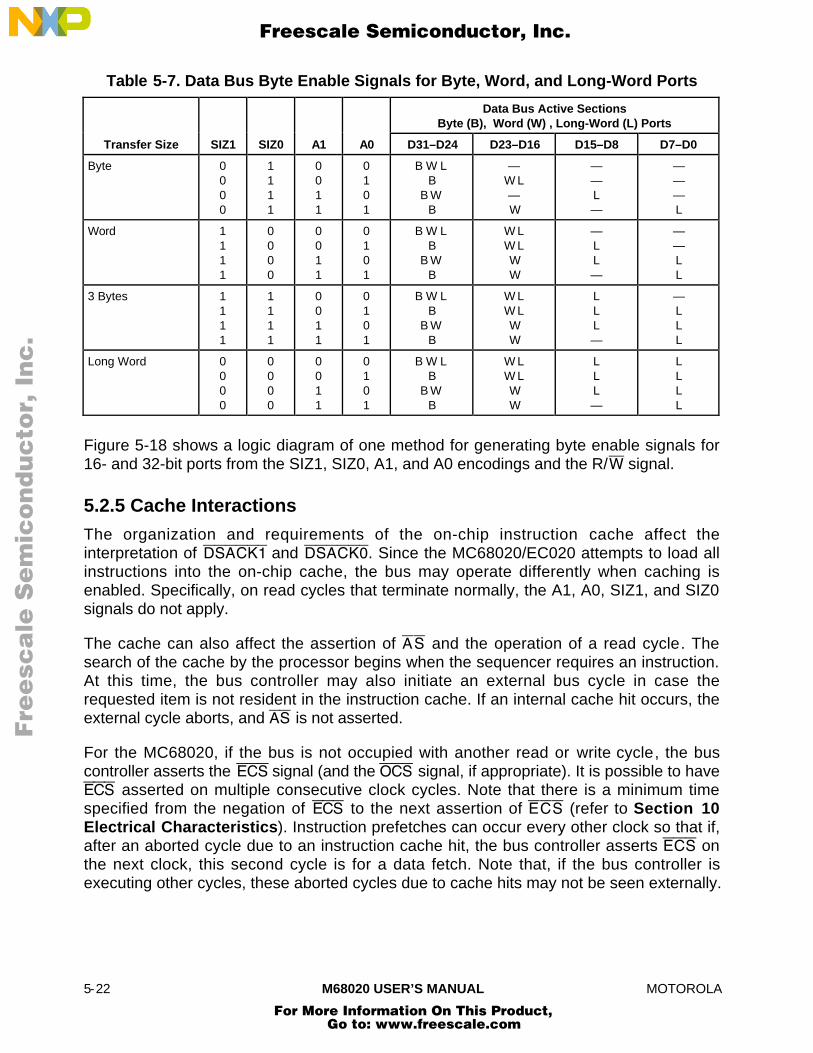
5-22 M68020 USER’S MANUAL MOTOROLA
Table 5-7. Data Bus Byte Enable Signals for Byte, Word, and Long-Word Ports
Data Bus Active SectionsByte (B), Word (W) , Long-Word (L) Ports
Transfer Size SIZ1 SIZ0 A1 A0 D31–D24 D23–D16 D15–D8 D7–D0
Byte 0000
1111
0011
0101
B W LB
B WB
—W L—W
——L—
———L
Word 1111
0000
0011
0101
B W LB
B WB
W LW LWW
—LL—
——LL
3 Bytes 1111
1111
0011
0101
B W LB
B WB
W LW LWW
LLL—
—LLL
Long Word 0000
0000
0011
0101
B W LB
B WB
W LW LWW
LLL—
LLLL
Figure 5-18 shows a logic diagram of one method for generating byte enable signals for16- and 32-bit ports from the SIZ1, SIZ0, A1, and A0 encodings and the R/W signal.
5.2.5 Cache Interactions
The organization and requirements of the on-chip instruction cache affect theinterpretation of DSACK1 and DSACK0. Since the MC68020/EC020 attempts to load allinstructions into the on-chip cache, the bus may operate differently when caching isenabled. Specifically, on read cycles that terminate normally, the A1, A0, SIZ1, and SIZ0signals do not apply.
The cache can also affect the assertion of AS and the operation of a read cycle. Thesearch of the cache by the processor begins when the sequencer requires an instruction.At this time, the bus controller may also initiate an external bus cycle in case therequested item is not resident in the instruction cache. If an internal cache hit occurs, theexternal cycle aborts, and AS is not asserted.
For the MC68020, if the bus is not occupied with another read or write cycle, the buscontroller asserts the ECS signal (and the OCS signal, if appropriate). It is possible to haveECS asserted on multiple consecutive clock cycles. Note that there is a minimum timespecified from the negation of ECS to the next assertion of ECS (refer to Section 10Electrical Characteristics). Instruction prefetches can occur every other clock so that if,after an aborted cycle due to an instruction cache hit, the bus controller asserts ECS onthe next clock, this second cycle is for a data fetch. Note that, if the bus controller isexecuting other cycles, these aborted cycles due to cache hits may not be seen externally.
Fre
esc
ale
Se
mic
on
du
cto
r, I
Freescale Semiconductor, Inc.
For More Information On This Product, Go to: www.freescale.com
nc
...

MOTOROLA M68020 USER’S MANUAL 5-23
A1
SIZ0
SIZ1
R/W
LD
UD
LLD
LMD
UMD
UUD
A0
UUDUMDLMDLLD UD LD
UPPER UPPER DATA (32-BIT PORT)UPPER MIDDLE DATA (32-BIT PORT)LOWER MIDDLE DATA (32-BIT PORT)LOWER LOWER DATA (32-BIT PORT)UPPER DATA (16-BIT PORT)LOWER DATA (16-BIT PORT)
== = = = =
Figure 5-18. Byte Enable Signal Generation for 16- and 32-Bit Ports
Fre
esc
ale
Se
mic
on
du
cto
r, I
Freescale Semiconductor, Inc.
For More Information On This Product, Go to: www.freescale.com
nc
...

5-24 M68020 USER’S MANUAL MOTOROLA
5.2.6 Bus Operation
The MC68020/EC020 bus is used in an asynchronous manner allowing external devicesto operate at clock frequencies different from the MC68020/EC020 clock. Bus operationuses the handshake lines (AS, DS, DSACK0, DSACK1, BERR, and HALT) to control datatransfers. AS signals the start of a bus cycle, and DS is used as a condition for valid dataon a write cycle. Decoding SIZ1, SIZ0, A1, and A0 provides byte enable signals that selectthe active portion of the data bus. The slave device (memory or peripheral) then respondsby placing the requested data on the correct portion of the data bus for a read cycle orlatching the data on a write cycle and by asserting the DSACK0/DSACK1 combination thatcorresponds to the port size to terminate the cycle. If no slave responds or the access isinvalid, external control logic asserts BERR to abort or BERR and HALT to retry the buscycle.
DSACK1/DSACK0 can be asserted before the data from a slave device is valid on a readcycle. The length of time that DSACK1/DSACK0 may precede data is given by parameter#31, and it must be met in any asynchronous system to ensure that valid data is latchedinto the processor. (Refer to Section 10 Electrical Characteristics for timingparameters.) Note that no maximum time is specified from the assertion of AS to theassertion of DSACK1/DSACK0. Although the processor can transfer data in a minimum ofthree clock cycles when the cycle is terminated with DSACK1/DSACK0, the processorinserts wait cycles in clock period increments until DSACK1/DSACK0 is recognized.
The BERR and/or HALT signals can be asserted after DSACK1/DSACK0 is asserted.BERR and/or HALT must be asserted within the time given (parameter #48), afterDSACK1/DSACK0 is asserted in any asynchronous system. If this maximum delay time isviolated, the processor may exhibit erratic behavior.
5.2.7 Synchronous Operation with DSACK1/DSACK0
Although cycles terminated with DSACK1/DSACK0 are classified as asynchronous, cyclesterminated with DSACK1/DSACK0 can also operate synchronously in that signals areinterpreted relative to clock edges. The devices that use these synchronous cycles mustsynchronize the responses to the MC68020/EC020 clock. Since these devices terminatebus cycles with DSACK1/DSACK0 , the dynamic bus sizing capabilities of theMC68020/EC020 are available. In addition, the minimum cycle time for these synchronouscycles is three clocks.
To support systems that use the system clock to generate DSACK1/DSACK0 and otherasynchronous inputs, the asynchronous input setup time (parameter #47A) and theasynchronous input hold time (parameter #47B) are provided in Section 10 ElectricalCharacteristics. (Note: although a misnomer, these “asynchronous” parameters are thesetup and hold times for synchronous operation.) If the setup and hold times are met forthe assertion or negation of a signal, such as DSACK1/DSACK0, the processor can beguaranteed to recognize that signal level on that specific falling edge of the system clock.If the assertion of DSACK1/DSACK0 is recognized on a particular falling edge of the clock,valid data is latched into the processor (for a read cycle) on the next falling clock edgeprovided the data meets the data setup time (parameter #27). In this case, parameter #31
Fre
esc
ale
Se
mic
on
du
cto
r, I
Freescale Semiconductor, Inc.
For More Information On This Product, Go to: www.freescale.com
nc
...
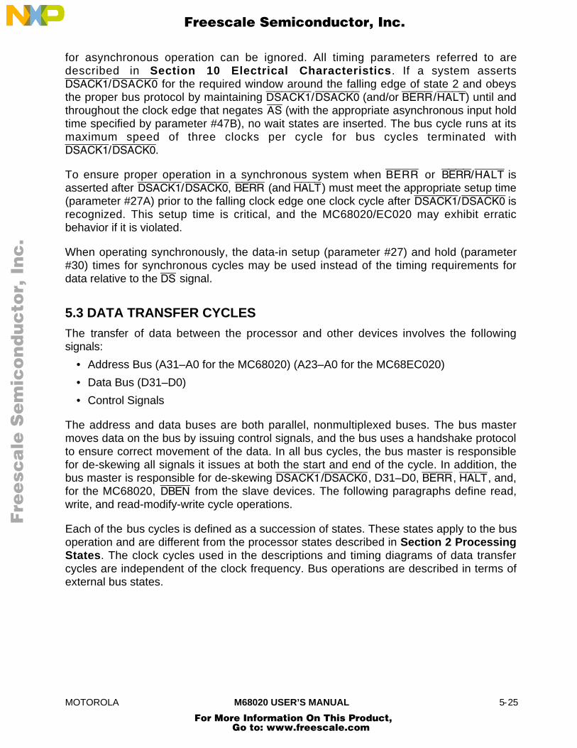
MOTOROLA M68020 USER’S MANUAL 5-25
for asynchronous operation can be ignored. All timing parameters referred to aredescribed in Section 10 Electrical Characteristics. If a system assertsDSACK1/DSACK0 for the required window around the falling edge of state 2 and obeysthe proper bus protocol by maintaining DSACK1/DSACK0 (and/or BERR/HALT) until andthroughout the clock edge that negates AS (with the appropriate asynchronous input holdtime specified by parameter #47B), no wait states are inserted. The bus cycle runs at itsmaximum speed of three clocks per cycle for bus cycles terminated withDSACK1/DSACK0.
To ensure proper operation in a synchronous system when BERR or BERR/HALT isasserted after DSACK1/DSACK0, BERR (and HALT) must meet the appropriate setup time(parameter #27A) prior to the falling clock edge one clock cycle after DSACK1/DSACK0 isrecognized. This setup time is critical, and the MC68020/EC020 may exhibit erraticbehavior if it is violated.
When operating synchronously, the data-in setup (parameter #27) and hold (parameter#30) times for synchronous cycles may be used instead of the timing requirements fordata relative to the DS signal.
5.3 DATA TRANSFER CYCLES
The transfer of data between the processor and other devices involves the followingsignals:
• Address Bus (A31–A0 for the MC68020) (A23–A0 for the MC68EC020)
• Data Bus (D31–D0)
• Control Signals
The address and data buses are both parallel, nonmultiplexed buses. The bus mastermoves data on the bus by issuing control signals, and the bus uses a handshake protocolto ensure correct movement of the data. In all bus cycles, the bus master is responsiblefor de-skewing all signals it issues at both the start and end of the cycle. In addition, thebus master is responsible for de-skewing DSACK1/DSACK0, D31–D0, BERR, HALT, and,for the MC68020, DBEN from the slave devices. The following paragraphs define read,write, and read-modify-write cycle operations.
Each of the bus cycles is defined as a succession of states. These states apply to the busoperation and are different from the processor states described in Section 2 ProcessingStates. The clock cycles used in the descriptions and timing diagrams of data transfercycles are independent of the clock frequency. Bus operations are described in terms ofexternal bus states.
Fre
esc
ale
Se
mic
on
du
cto
r, I
Freescale Semiconductor, Inc.
For More Information On This Product, Go to: www.freescale.com
nc
...
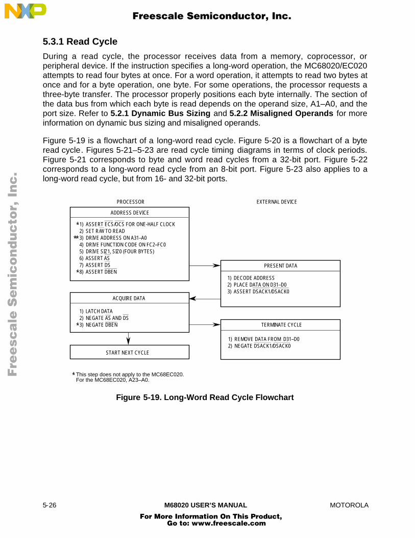
5-26 M68020 USER’S MANUAL MOTOROLA
5.3.1 Read Cycle
During a read cycle, the processor receives data from a memory, coprocessor, orperipheral device. If the instruction specifies a long-word operation, the MC68020/EC020attempts to read four bytes at once. For a word operation, it attempts to read two bytes atonce and for a byte operation, one byte. For some operations, the processor requests athree-byte transfer. The processor properly positions each byte internally. The section ofthe data bus from which each byte is read depends on the operand size, A1–A0, and theport size. Refer to 5.2.1 Dynamic Bus Sizing and 5.2.2 Misaligned Operands for moreinformation on dynamic bus sizing and misaligned operands.
Figure 5-19 is a flowchart of a long-word read cycle. Figure 5-20 is a flowchart of a byteread cycle. Figures 5-21–5-23 are read cycle timing diagrams in terms of clock periods.Figure 5-21 corresponds to byte and word read cycles from a 32-bit port. Figure 5-22corresponds to a long-word read cycle from an 8-bit port. Figure 5-23 also applies to along-word read cycle, but from 16- and 32-bit ports.
PROCESSOR
ADDRESS DEVICE
1) ASSERT ECS/OCS FOR ONE-HALF CLOCK2) SET R/W TO READ3) DRIVE ADDRESS ON A31–A04) DRIVE FUNCTION CODE ON FC2–FC05) DRIVE SIZ1, SIZ0 (FOUR BYTES)6) ASSERT AS7) ASSERT DS8) ASSERT DBEN
ACQUIRE DATA
1) LATCH DATA2) NEGATE AS AND DS3) NEGATE DBEN
START NEXT CYCLE
PRESENT DATA
1) DECODE ADDRESS2) PLACE DATA ON D31–D03) ASSERT DSACK1/DSACK0
TERMINATE CYCLE
1) REMOVE DATA FROM D31–D02) NEGATE DSACK1/DSACK0
EXTERNAL DEVICE
*
*
* This step does not apply to the MC68EC020.For the MC68EC020, A23–A0.
*
**
Figure 5-19. Long-Word Read Cycle Flowchart
Fre
esc
ale
Se
mic
on
du
cto
r, I
Freescale Semiconductor, Inc.
For More Information On This Product, Go to: www.freescale.com
nc
...
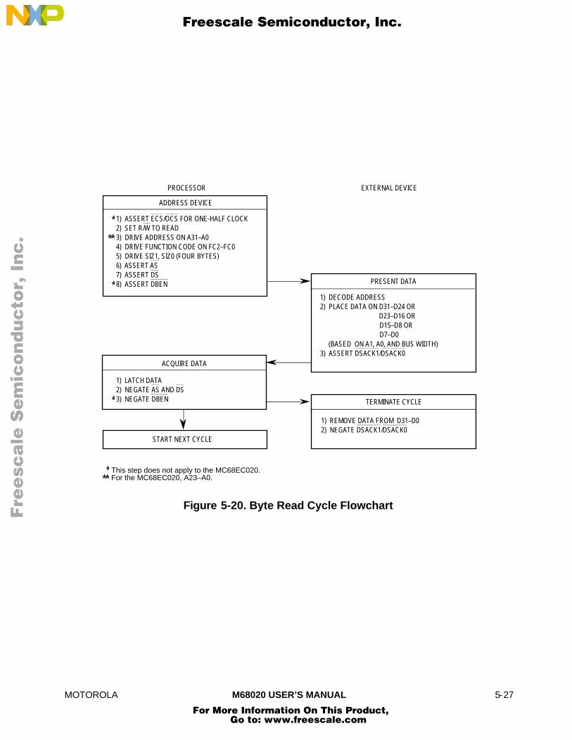
MOTOROLA M68020 USER’S MANUAL 5-27
ACQUIRE DATA
1) LATCH DATA2) NEGATE AS AND DS3) NEGATE DBEN
START NEXT CYCLE
PRESENT DATA
1) DECODE ADDRESS2) PLACE DATA ON D31–D24 OR D23–D16 OR D15–D8 OR D7–D0 (BASED ON A1, A0, AND BUS WIDTH)3) ASSERT DSACK1/DSACK0
TERMINATE CYCLE
1) REMOVE DATA FROM D31–D02) NEGATE DSACK1/DSACK0
EXTERNAL DEVICEPROCESSOR
ADDRESS DEVICE
1) ASSERT ECS/OCS FOR ONE-HALF CLOCK2) SET R/W TO READ3) DRIVE ADDRESS ON A31–A04) DRIVE FUNCTION CODE ON FC2–FC05) DRIVE SIZ1, SIZ0 (FOUR BYTES)6) ASSERT AS7) ASSERT DS8) ASSERT DBEN*
* This step does not apply to the MC68EC020.For the MC68EC020, A23–A0.**
*
**
*
Figure 5-20. Byte Read Cycle Flowchart
Fre
esc
ale
Se
mic
on
du
cto
r, I
Freescale Semiconductor, Inc.
For More Information On This Product, Go to: www.freescale.com
nc
...

5-28 M68020 USER’S MANUAL MOTOROLA
WORD READ
S0 S2 S4 S0 S2 S4
CLK
A31–A2
A1
A0
FC2–FC0
SIZ1
SIZ0
R/W
ECS
OCS
AS
DS
DSACK1
DSACK0
DBEN
D31–D24
D23–D16
BYTE READ
D15–D8
D7–D0
S0 S2 S4
OP2
OP3
OP3
OP3
WORD BYTE
BYTE READ
**
**
**
*
*
Figure 5-21. Byte and Word Read Cycles—32-Bit Port
Fre
esc
ale
Se
mic
on
du
cto
r, I
Freescale Semiconductor, Inc.
For More Information On This Product, Go to: www.freescale.com
nc
...

MOTOROLA M68020 USER’S MANUAL 5-29
BYTE READ
A31–A2
A1
A0
FC2–FC0
SIZ1
SIZ0
R/W
ECS
OCS
AS
DS
DSACK1
DSACK0
DBEN
D31–D24
D23–D16
D15–D8
D7–D0
OP0 OP1 OP3
LONG WORD 3-BYTE
BYTE READ
CLK
WORD BYTE
OP2
BYTE READBYTE READ
LONG-WORD OPERAND READ FROM 8-BIT PORT
S0 S2 S4 S0 S2 S4 S0 S2 S4 S0 S2 S4
**
**
**
*
* For the MC68EC020, A23–A2.This signal does not apply to the MC68EC020.
Figure 5-22. Long-Word Read—8-Bit Port
Fre
esc
ale
Se
mic
on
du
cto
r, I
Freescale Semiconductor, Inc.
For More Information On This Product, Go to: www.freescale.com
nc
...
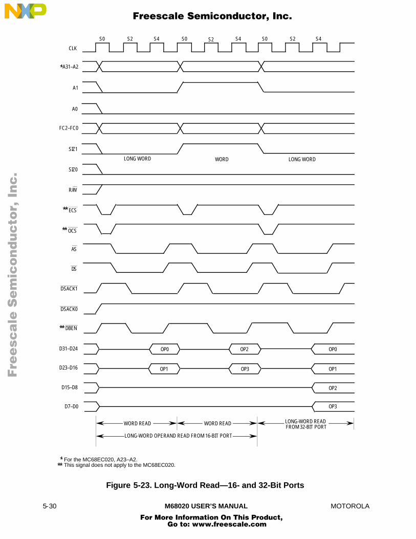
5-30 M68020 USER’S MANUAL MOTOROLA
WORD READ
S0 S2 S4 S0 S2 S4
CLK
A31–A2
A1
A0
FC2–FC0
SIZ1
SIZ0
R/W
ECS
OCS
AS
DS
DSACK1
DSACK0
DBEN
D31–D24
D23–D16
WORD READ
D15–D8
D7–D0
S0 S2 S4
OP0
OP1 OP3
OP3
LONG WORD WORD
LONG-WORD READFROM 32-BIT PORT
OP2
OP1
OP0OP2
LONG WORD
LONG-WORD OPERAND READ FROM 16-BIT PORT
**
**
**
*
* For the MC68EC020, A23–A2.This signal does not apply to the MC68EC020.**
Figure 5-23. Long-Word Read—16- and 32-Bit Ports
Fre
esc
ale
Se
mic
on
du
cto
r, I
Freescale Semiconductor, Inc.
For More Information On This Product, Go to: www.freescale.com
nc
...

MOTOROLA M68020 USER’S MANUAL 5-31
State 0MC68020—The read cycle starts in state 0 (S0). The processor asserts ECS, indicatingthe beginning of an external cycle. If the cycle is the first external cycle of a readoperation, OCS is asserted simultaneously. During S0, the processor places a validaddress on A31–A0 and valid function codes on FC2–FC0. The function codes selectthe address space for the cycle. The processor drives R/W high for a read cycle andnegates DBEN to disable the data buffers. SIZ0 and SIZ1 become valid, indicating thenumber of bytes requested to be transferred.
MC68EC020—The read cycle starts in S0. During S0, the processor places a validaddress on A23–A0 and valid function codes on FC2–FC0. The function codes selectthe address space for the cycle. The processor drives R/W high for a read cycle. SIZ0and SIZ1 become valid, indicating the number of bytes requested to be transferred.
State 1MC68020—One-half clock later in state 1 (S1), the processor asserts AS, indicating thatthe address on the address bus is valid. The processor also asserts DS during S1. Inaddition, the ECS (and OCS , if asserted) signal is negated during S1.
MC68EC020—One-half clock later in S1, the processor asserts AS, indicating that theaddress on the address bus is valid. The processor also asserts DS during S1.
State 2MC68020—During state 2 (S2), the processor asserts DBEN to enable external databuffers. The selected device uses R/W, SIZ1–SIZ0, A1–A0, and DS to place itsinformation on the data bus. Any or all of the bytes (D31–D24, D23–D16, D15–D8, andD7–D0) are selected by SIZ1–SIZ0 and A1–A0. Concurrently, the selected deviceasserts DSACK1/DSACK0 .
MC68EC020—During S2, the selected device uses R/W, SIZ1–SIZ0, A1–A0, and DS toplace its information on the data bus. Any or all of the bytes (D31–D24, D23–D16,D15–D8, and D7–D0) are selected by SIZ1–SIZ0 and A1–A0. Concurrently, theselected device asserts DSACK1/DSACK0.
State 3MC68020/EC020—As long as at least one of the DSACK1/DSACK0 signals isrecognized by the end of S2 (meeting the asynchronous input setup time requirement),data is latched on the next falling edge of the clock, and the cycle terminates. IfDSACK1/DSACK0 is not recognized by the start of state 3 (S3), the processor insertswait states instead of proceeding to states 4 and 5. To ensure that wait states areinserted, both DSACK1 and D S A C K 0 must remain negated throughout theasynchronous input setup and hold times around the end of S2. If wait states areadded, the processor continues to sample the DSACK1/DSACK0 signals on the fallingedges of the clock until an assertion is recognized.
Fre
esc
ale
Se
mic
on
du
cto
r, I
Freescale Semiconductor, Inc.
For More Information On This Product, Go to: www.freescale.com
nc
...
5-32 M68020 USER’S MANUAL MOTOROLA
State 4MC68020/EC020—At the end of state 4 (S4), the processor latches the incoming data.
State 5MC68020—The processor negates AS, DS, and DBEN during state 5 (S5). It holds theaddress valid during S5 to provide address hold time for memory systems. R/W, SIZ1–SIZ0, and FC2–FC0 also remain valid throughout S5.The external device keeps its data and DSACK1/DSACK0 signals asserted until itdetects the negation of AS or DS (whichever it detects first). The device must removeits data and negate DSACK1/DSACK0 within approximately one clock period aftersensing the negation of AS or DS. DSACK1/DSACK0 signals that remain assertedbeyond this limit may be prematurely detected for the next bus cycle.
MC68EC020—The processor negates AS and DS during state S5. It holds the addressvalid during S5 to provide address hold time for memory systems. R/W , SIZ1, SIZ0,and FC2–FC0 also remain valid throughout S5.The external device keeps its data and DSACK1/DSACK0 signals asserted until itdetects the negation of AS or DS (whichever it detects first). The device must removeits data and negate DSACK1/DSACK0 within approximately one clock period aftersensing the negation of AS or DS. DSACK1/DSACK0 signals that remain assertedbeyond this limit may be prematurely detected for the next bus cycle.
Fre
esc
ale
Se
mic
on
du
cto
r, I
Freescale Semiconductor, Inc.
For More Information On This Product, Go to: www.freescale.com
nc
...

MOTOROLA M68020 USER’S MANUAL 5-33
5.3.2 Write Cycle
During a write cycle, the processor transfers data to memory or a peripheral device.Figure 5-24 is a flowchart of a write cycle operation for a long-word transfer. Figures 5-25–5-28 are write cycle timing diagrams in terms of clock periods. Figure 5-25 shows twowrite cycles (between two read cycles with no idle time in between) for a 32-bit port.Figure 5-26 shows byte and word write cycles to a 32-bit port. Figure 5-27 shows a long-word write cycle to an 8-bit port. Figure 5-28 shows a long-word write cycle to a 16-bitport.
1) ASSERT ECS/OCS FOR ONE-HALF CLOCK2) DRIVE ADDRESS ON A31–A03) DRIVE FUNCTION CODES ON FC2–FC04) DRIVE SIZ1, SIZ0 (FOUR BYTES) 5) SET R/W TO WRITE6) ASSERT AS7) ASSERT DBEN8) DRIVE DATA LINES D31–D09) ASSERT DS
1) NEGATE AS AND DS 2) REMOVE DATA FROM D31–D03) NEGATE DBEN
EXTERNAL DEVICEPROCESSOR
1) NEGATE DSACK1/DSACK0
TERMINATE CYCLE
ACCEPT DATA
1) DECODE ADDRESS2) STORE DATA FROM D31–D03) ASSERT DSACK1/DSACK0
ADDRESS DEVICE
TERMINATE OUTPUT TRANSFER
START NEXT CYCLE
*
* This step does not apply to the MC68EC020.For the MC68EC020, A23–A0.**
***
*
Figure 5-24. Write Cycle Flowchart
Fre
esc
ale
Se
mic
on
du
cto
r, I
Freescale Semiconductor, Inc.
For More Information On This Product, Go to: www.freescale.com
nc
...
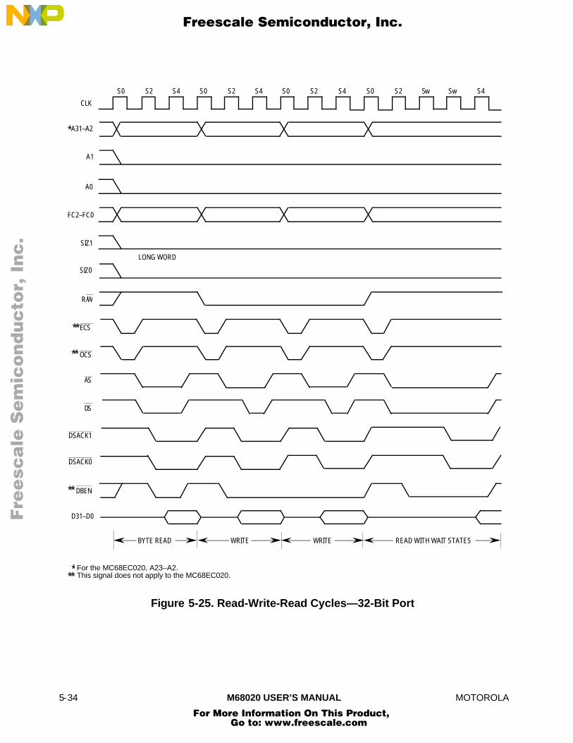
5-34 M68020 USER’S MANUAL MOTOROLA
WRITE
A31–A2
A1
A0
FC2–FC0
SIZ1
SIZ0
R/W
ECS
OCS
AS
DS
DSACK1
DSACK0
DBEN
D31–D0
LONG WORD
CLK
WRITEBYTE READ
S0 S2 S4 S0 S2 S4 S0 S2 S4 S0 S2 Sw Sw S4
READ WITH WAIT STATES
**
**
**
*
* For the MC68EC020, A23–A2.This signal does not apply to the MC68EC020.**
Figure 5-25. Read-Write-Read Cycles—32-Bit Port
Fre
esc
ale
Se
mic
on
du
cto
r, I
Freescale Semiconductor, Inc.
For More Information On This Product, Go to: www.freescale.com
nc
...

MOTOROLA M68020 USER’S MANUAL 5-35
WORD WRITE
S0 S2 S4 S0 S2 S4
CLK
A31-A2
A1
A0
FC2–FC0
SIZ1
SIZ0
R/W
ECS
OCS
AS
DS
DSACK1
DSACK0
DBEN
D31–D24
D23–D16
BYTE WRITE
D15–D8
D7–D0
S0 S2 S4
OP2
OP3 OP3
OP3
WORD
OP3
OP3
OP3OP3
BYTE
OP2
OP3 OP3
OP3
BYTE WRITE
**
**
**
*
* For the MC68EC020, A23–A2.This signal does not apply to the MC68EC020.
Figure 5-26. Byte and Word Write Cycles—32-Bit Port
Fre
esc
ale
Se
mic
on
du
cto
r, I
Freescale Semiconductor, Inc.
For More Information On This Product, Go to: www.freescale.com
nc
...

5-36 M68020 USER’S MANUAL MOTOROLA
BYTE WRITE
A31–A2
A1
A0
FC2–FC0
SIZ1
SIZ0
R/W
ECS
OCS
AS
DS
DSACK1
DSACK0
DBEN
D31–D24
D23–D16
D15–D8
D7–D0
LONG WORD 3-BYTE
BYTE WRITE
CLK
WORD BYTE
BYTE WRITEBYTE WRITE
LONG-WORD OPERAND WRITE TO 8-BIT PORT
S0 S2 S4 S0 S2 S4 S0 S2 S4 S0 S2 S4
OP0 OP3OP2OP1
OP1 OP3OP3OP1
OP2 OP3OP2OP2
OP3 OP3OP3OP3
**
**
**
*
* For the MC68EC020, A23–A2.This signal does not apply to the MC68EC020.
Figure 5-27. Long-Word Operand Write—8-Bit Port
Fre
esc
ale
Se
mic
on
du
cto
r, I
Freescale Semiconductor, Inc.
For More Information On This Product, Go to: www.freescale.com
nc
...

MOTOROLA M68020 USER’S MANUAL 5-37
WORD WRITE
S0 S2 S4 S0 S2 S4
CLK
A31–A2
A1
A0
FC2–FC0
SIZ1
SIZ0
R/W
ECS
OCS
AS
DS
DSACK1
DSACK0
DBEN
D31–D24
D23–D16
WORD WRITE
D15–D8
D7–D0
S0 S2 S4
OP0
OP1 OP3
OP3
LONG WORD
OP2
OP1
OP0OP2
WORD
OP2
OP3 OP3
OP2
LONG-WORD WRITETO 32-BIT PORT
LONG-WORD OPERAND WRITE TO 16-BIT PORT
**
**
**
*
* For the MC68EC020, A23–A2.This signal does not apply to the MC68EC020.**
LONG WORD
Figure 5-28. Long-Word Operand Write—16-Bit Port
Fre
esc
ale
Se
mic
on
du
cto
r, I
Freescale Semiconductor, Inc.
For More Information On This Product, Go to: www.freescale.com
nc
...

5-38 M68020 USER’S MANUAL MOTOROLA
State 0MC68020—The write cycle starts in S0. The processor negates ECS, indicating thebeginning of an external cycle. If the cycle is the first external cycle of a writeoperation, OCS is asserted simultaneously. During S0, the processor places a validaddress on A31–A0 and valid function codes on FC2–FC0. The function codes selectthe address space for the cycle. The processor drives R/W low for a write cycle. SIZ1–SIZ0 become valid, indicating the number of bytes to be transferred.
MC68EC020—The write cycle starts in S0. During S0, the processor places a validaddress on A23–A0 and valid function codes on FC2–FC0. The function codes selectthe address space for the cycle. The processor drives R/W low for a write cycle. SIZ1,SIZ0 become valid, indicating the number of bytes to be transferred.
State 1MC68020—One-half clock later in S1, the processor asserts AS, indicating that theaddress on the address bus is valid. The processor also asserts DBEN during S1,which can enable external data buffers. In addition, the ECS (and OCS , if asserted)signal is negated during S1.
MC68EC020—One-half clock later in S1, the processor asserts AS, indicating that theaddress on the address bus is valid.
State 2MC68020/EC020—During S2, the processor places the data to be written onto D31–D0.At the end of S2, the processor samples DSACK1/DSACK0 .
State 3MC68020/EC020—The processor asserts DS during S3, indicating that the data on thedata bus is stable. As long as at least one of the DSACK1/DSACK0 signals isrecognized by the end of S2 (meeting the asynchronous input setup time requirement),the cycle terminates one clock later. If DSACK1/DSACK0 is not recognized by the startof S3, the processor inserts wait states instead of proceeding to S4 and S5. To ensurethat wait states are inserted, both DSACK1 and DSACK0 must remain negatedthroughout the asynchronous input setup and hold times around the end of S2. If waitstates are added, the processor continues to sample the DSACK1/DSACK0 signals onthe falling edges of the clock until one is recognized.The external device uses R/W , DS, SIZ1, SIZ0, A1, and A0 to latch data from theappropriate byte(s) of the data bus (D31–D24, D23–D16, D15–D8, and D7–D0). SIZ1,SIZ0, A1, and A0 select the bytes of the data bus. If it has not already done so, thedevice asserts DSACK1/DSACK0 to signal that it has successfully stored the data.
Fre
esc
ale
Se
mic
on
du
cto
r, I
Freescale Semiconductor, Inc.
For More Information On This Product, Go to: www.freescale.com
nc
...
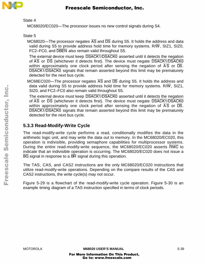
MOTOROLA M68020 USER’S MANUAL 5-39
State 4MC68020/EC020—The processor issues no new control signals during S4.
State 5MC68020—The processor negates AS and DS during S5. It holds the address and datavalid during S5 to provide address hold time for memory systems. R/W , SIZ1, SIZ0,FC2–FC0, and DBEN also remain valid throughout S5.The external device must keep DSACK1/DSACK0 asserted until it detects the negationof AS or DS (whichever it detects first). The device must negate DSACK1/DSACK0
within approximately one clock period after sensing the negation of A S or DS.DSACK1/DSACK0 signals that remain asserted beyond this limit may be prematurelydetected for the next bus cycle.
MC68EC020—The processor negates AS and DS during S5. It holds the address anddata valid during S5 to provide address hold time for memory systems. R/W , SIZ1,SIZ0, and FC2–FC0 also remain valid throughout S5.The external device must keep DSACK1/DSACK0 asserted until it detects the negationof AS or DS (whichever it detects first). The device must negate DSACK1/DSACK0
within approximately one clock period after sensing the negation of A S or DS.DSACK1/DSACK0 signals that remain asserted beyond this limit may be prematurelydetected for the next bus cycle.
5.3.3 Read-Modify-Write Cycle
The read-modify-write cycle performs a read, conditionally modifies the data in thearithmetic logic unit, and may write the data out to memory. In the MC68020/EC020, thisoperation is indivisible, providing semaphore capabilities for multiprocessor systems.During the entire read-modify-write sequence, the MC68020/EC020 asserts RMC toindicate that an indivisible operation is occurring. The MC68020/EC020 does not issue aBG signal in response to a BR signal during this operation.
The TAS, CAS, and CAS2 instructions are the only MC68020/EC020 instructions thatutilize read-modify-write operations. Depending on the compare results of the CAS andCAS2 instructions, the write cycle(s) may not occur.
Figure 5-29 is a flowchart of the read-modify-write cycle operation. Figure 5-30 is anexample timing diagram of a TAS instruction specified in terms of clock periods.
Fre
esc
ale
Se
mic
on
du
cto
r, I
Freescale Semiconductor, Inc.
For More Information On This Product, Go to: www.freescale.com
nc
...

5-40 M68020 USER’S MANUAL MOTOROLA
LOCK BUS
1) ASSERT RMC
ADDRESS DEVICE
1) ASSERT ECS/OCS FOR ONE-HALF CLOCK2) SET R/W TO READ3) DRIVE ADDRESS ON A31–A04) DRIVE FUNCTION CODES ON FC2–FC05) DRIVE SIZ1, SIZ06) ASSERT AS 7) ASSERT DS8) ASSERT DBEN
ACQUIRE DATA
1) LATCH DATA2) NEGATE AS AND DS3) NEGATE DBEN 4) START DATA MODIFICATION
START OUTPUT TRANSFER
1) ASSERT ECS/OCS FOR ONE-HALF CLOCK2) DRIVE ADDRESS ON A31–A0 (IF DIFFERENT)3) DRIVE SIZ1, SIZ04) SET R/W TO WRITE 5) ASSERT AS6) ASSERT DBEN7) PLACE DATA ON D31–D08) ASSERT DS
TERMINATE OUTPUT TRANSFER
1) NEGATE AS AND DS2) REMOVE DATA FROM D31–D0 3) NEGATE DBEN
UNLOCK BUS
1) NEGATE RMC
START NEXT CYCLE
PRESENT DATA
1) DECODE ADDRESS2) PLACE DATA ON D31–D03) ASSERT DSACK1/DSACK0
TERMINATE CYCLE
1) REMOVE DATA FROM D31–D02) NEGATE DSACK1/DSACK0
ACCEPT DATA
1) DECODE ADDRESS2) STORE DATA FROM D31–D03) ASSERT DSACK1/DSACK0
TERMINATE CYCLE
A
IF CAS2 INSTRUCTIONAND ONLY ONE OPERANDREAD, THEN GO TO A ;IF OPERANDS DO NOT MATCH, THEN GO TO
C ; ELSE GO TO BC
B
1) NEGATE DSACK1/DSACK0
IF CAS2 INSTRUCTIONAND ONLY ONE OPERAND
WRITTEN, THEN GO TO D ; ELSE GO TO E
E
D
PROCESSOR EXTERNAL DEVICE
* This step does not apply to the MC68EC020.For the MC68EC020, A23–A0.**
*
**
*
*
*
***
*
Figure 5-29. Read-Modify-Write Cycle Flowchart
Fre
esc
ale
Se
mic
on
du
cto
r, I
Freescale Semiconductor, Inc.
For More Information On This Product, Go to: www.freescale.com
nc
...
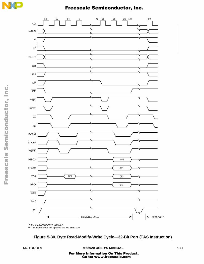
MOTOROLA M68020 USER’S MANUAL 5-41
INDIVISIBLE CYCLE NEXT CYCLE
CLK
A31–A2
A1
A0
FC2–FC0
SIZ1
R/W
AS
DS
DSACK0
DBEN
D31–D24
SIZ0
DSACK1
S0 S2 S4 Si S6 S8 S10 S0
D7–D0
D23–D16
RMC
ECS
OP3
OP3
OP3OP3
OP3
BERR
HALT
BG
D15–8
S11
**
**
**
*
* For the MC68EC020, A23–A2.This signal does not apply to the MC68EC020.**
Si
OCS
Figure 5-30. Byte Read-Modify-Write Cycle—32-Bit Port (TAS Instruction)
Fre
esc
ale
Se
mic
on
du
cto
r, I
Freescale Semiconductor, Inc.
For More Information On This Product, Go to: www.freescale.com
nc
...
5-42 M68020 USER’S MANUAL MOTOROLA
State 0MC68020—The processor asserts ECS and OCS in S0 to indicate the beginning of anexternal operand cycle. The processor also asserts RMC in S0 to identify a read-modify-write cycle. The processor places a valid address on A31–A0 and valid functioncodes on FC2–FC0. The function codes select the address space for the operation.SIZ1, SIZ0 become valid in S0 to indicate the operand size. The processor drives R/Whigh for the read cycle.
MC68EC020—The processor asserts RMC in S0 to identify a read-modify-write cycle.The processor places a valid address on A23–A0 and valid function codes on FC2–FC0. The function codes select the address space for the operation. SIZ1–SIZ0become valid in S0 to indicate the operand size. The processor drives R/W high for theread cycle.
State 1MC68020—One-half clock later in S1, the processor asserts AS to indicate that theaddress on the address bus is valid. The processor also asserts DS during S1. Inaddition, the ECS (and OCS , if asserted) signal is negated during S1.
MC68EC020—One-half clock later in S1, the processor asserts AS to indicate that theaddress on the address bus is valid. The processor also asserts DS during S1.
State 2MC68020—During S2, the processor asserts DBEN to enable external data buffers. Theselected device uses R/W , SIZ1, SIZ0, A1, A0, and DS to place information on thedata bus. Any or all of the bytes (D31–D24, D23–D16, D15–D8, and D7–D0) areselected by SIZ1, SIZ0, A1, and A0. Concurrently, the selected device may assert theDSACK1/DSACK0 signals.
MC68EC020—During S2, the selected device uses R/W, SIZ1, SIZ0, A1, A0, and DS toplace information on the data bus. Any or all of the bytes (D31–D24, D23–D16, D15–D8, and D7–D0) are selected by SIZ1, SIZ0, A1, and A0. Concurrently, the selecteddevice may assert the DSACK1/DSACK0 signals.
State 3MC68020/EC020—As long as at least one of the DSACK1/DSACK0 signals isrecognized by the end of S2 (meeting the asynchronous input setup time requirement),data is latched on the next falling edge of the clock, and the cycle terminates. IfDSACK1/DSACK0 is not recognized by the start of S3, the processor inserts waitstates instead of proceeding to S4 and S5. To ensure that wait states are inserted,both DSACK0 and DSACK1 must remain negated throughout the asynchronous inputsetup and hold times around the end of S2. If wait states are added, the processorcontinues to sample the DSACK1/DSACK0 signals on the falling edges of the clockuntil one is recognized.
State 4MC68020/EC020—At the end of S4, the processor latches the incoming data.
Fre
esc
ale
Se
mic
on
du
cto
r, I
Freescale Semiconductor, Inc.
For More Information On This Product, Go to: www.freescale.com
nc
...

MOTOROLA M68020 USER’S MANUAL 5-43
State 5MC68020—The processor negates AS, DS, and DBEN during S5. If more than one readcycle is required to read in the operand(s), S0–S5 are repeated for each read cycle.When the read cycle(s) are complete, the processor holds the address, R/W , andFC2–FC0 valid in preparation for the write portion of the cycle.The external device keeps its data and DSACK1/DSACK0 signals asserted until itdetects the negation of AS or DS (whichever it detects first). The device must removethe data and negate DSACK1/DSACK0 within approximately one clock period aftersensing the negation of AS or DS. DSACK1/DSACK0 signals that remain assertedbeyond this limit may be prematurely detected for the next portion of the operation.
MC68EC020—The processor negates AS, DS, and DBEN during S5. If more than oneread cycle is required to read in the operand(s), S0–S5 are repeated for each readcycle. When the read cycle(s) is complete, the processor holds the address, R/W, andFC2–FC0 valid in preparation for the write portion of the cycle.The external device keeps its data and DSACK1/DSACK0 signals asserted until itdetects the negation of AS or DS (whichever it detects first). The device must removethe data and negate DSACK1/DSACK0 within approximately one clock period aftersensing the negation of AS or DS. DSACK1/DSACK0 signals that remain assertedbeyond this limit may be prematurely detected for the next portion of the operation.
Idle StatesMC68020/EC020—The processor does not assert any new control signals during theidle states, but it may internally begin the modify portion of the cycle at this time. S6–S11 are omitted if no write cycle is required. If a write cycle is required, the R/W signalremains in the read mode until S6 to prevent bus conflicts with the preceding readportion of the cycle; the data bus is not driven until S8.
State 6MC68020—The processor asserts ECS and OCS in S6 to indicate that another externalcycle is beginning. The processor drives R/W low for a write cycle. Depending on thewrite operation to be performed, the address lines may change during S6.
MC68EC020—During S6, the processor drives R/W low for a write cycle. Depending onthe write operation to be performed, the address lines may change during S6.
State 7MC68020—During S7, the processor asserts AS, indicating that the address on theaddress bus is valid. The processor also asserts DBEN, which can be used to enabledata buffers. In addition, ECS (and OCS, if asserted) is negated during S7.
MC68EC020—During S7, the processor asserts AS, indicating that the address on theaddress bus is valid.
State 8MC68020/EC020—During S8, the processor places the data to be written onto the databus.
Fre
esc
ale
Se
mic
on
du
cto
r, I
Freescale Semiconductor, Inc.
For More Information On This Product, Go to: www.freescale.com
nc
...

5-44 M68020 USER’S MANUAL MOTOROLA
State 9MC68020/EC020—The processor asserts DS during S9, indicating that the data on thedata bus is stable. As long as at least one of the DSACK1/DSACK0 signals isrecognized by the end of S8 (meeting the asynchronous input setup time requirement),the cycle terminates one clock later. If DSACK1/DSACK0 is not recognized by the startof S9, the processor inserts wait states instead of proceeding to S10 and S11. Toensure that wait states are inserted, both DSACK1 and DSACK0 must remain negatedthroughout the asynchronous input setup and hold times around the end of S8. If waitstates are added, the processor continues to sample DSACK1/DSACK0 signals on thefalling edges of the clock until one is recognized.The external device uses R/W , DS, SIZ1, SIZ0, A1, and A0 to latch data from theappropriate section(s) of the data bus (D31–D24, D23–D16, D15–D8, and D7–D0).SIZ1, SIZ0, A1, and A0 select the data bus sections. If it has not already done so, thedevice asserts DSACK1/DSACK0 when it has successfully stored the data.
State 10MC68020/EC020—The processor issues no new control signals during S10.
State 11MC68020/EC020—The processor negates AS and DS during S11. It holds the addressand data valid during S11 to provide address hold time for memory systems. R/W andFC2–FC0 also remain valid throughout S11.If more than one write cycle is required, S6–S11 are repeated for each write cycle.The external device keeps DSACK1/DSACK0 asserted until it detects the negation ofAS or DS (whichever it detects first). The device must remove its data and negateDSACK1/DSACK0 within approximately one clock period after sensing the negation ofAS or DS.
5.4 CPU SPACE CYCLES
FC2–FC0 select user and supervisor program and data areas as listed in Table 2-1. Thearea selected by FC2–FC0 = 111 is classified as the CPU space. The interruptacknowledge, breakpoint acknowledge, module operations, and coprocessorcommunication cycles described in the following paragraphs utilize CPU space.
The CPU space type is encoded on A19–A16 during a CPU space operation and indicatesthe function that the processor is performing. On the MC68020/EC020, four of theencodings are implemented as shown in Figure 5-31. All unused values are reserved byMotorola for future use.
Fre
esc
ale
Se
mic
on
du
cto
r, I
Freescale Semiconductor, Inc.
For More Information On This Product, Go to: www.freescale.com
nc
...

MOTOROLA M68020 USER’S MANUAL 5-45
1 1 1
1 1 1
1 1 1
1 1 1
BREAKPOINTACKNOWLEDGE
ACCESS LEVELCONTROL
COPROCESSORCOMMUNICATION
INTERRUPTACKNOWLEDGE 1 1 1 1 1 1 1 1 1 1 1 1 1 1 1 1 1 1 1 1 1 1 1 1 1 1 1 1 LEVEL 1
0 0 0 0 0 0 0 0 0 0 0 0 0 0 1 0 CpID 0 0 0 0 0 0 0 0 CP REG
15 13 4 0
3 1 031
31
0 0 0 0 0 0 0 0 0 0 0 0 0 0 0 1 0 0 0 0 0 0 0 0 0
6 0
MMU REG
BKPT # 0 0
31
31 4 2 0
0 0 0 0 0 0 0 0 0 0 00 0 0 0 0 0 0 0 0 0 0 0 0 0 0 0
19 16232 0
FUNCTION CODE
ADDRESS BUS
CPU SPACETYPE FIELD
24 20 15 5 1
719 1620 15
12161920
1920
5
41516
Figure 5-31. MC68020/EC020 CPU Space Address Encoding
5.4.1 Interrupt Acknowledge Bus Cycles
When a peripheral device signals the processor (with the IPL2–IPL0 signals) that thedevice requires service and when the internally synchronized value on these signalsindicates a higher priority than the interrupt mask in the status register (or that a transitionhas occurred in the case of a level 7 interrupt), the processor makes the interrupt apending interrupt. Refer to Section 6 Exception Processing for details on the recognitionof interrupts.
The MC68020/EC020 takes an interrupt exception for a pending interrupt within oneinstruction boundary (after processing any other pending exception with a higher priority).The following paragraphs describe the various kinds of interrupt acknowledge bus cyclesthat can be executed as part of interrupt exception processing.
5.4.1.1 INTERRUPT ACKNOWLEDGE CYCLE—TERMINATED NORMALLY. When theMC68020/EC020 processes an interrupt exception, it performs an interrupt acknowledgecycle to obtain the number of the vector that contains the starting location of the interruptservice routine.
Some interrupting devices have programmable vector registers that contain the interruptvectors for the routines they use. The following paragraphs describe the interruptacknowledge cycle for these devices. Other interrupting conditions or devices cannotsupply a vector number and use the autovector cycle described in 5.4.1.2 AutovectorInterrupt Acknowledge Cycle.
Fre
esc
ale
Se
mic
on
du
cto
r, I
Freescale Semiconductor, Inc.
For More Information On This Product, Go to: www.freescale.com
nc
...

5-46 M68020 USER’S MANUAL MOTOROLA
The interrupt acknowledge cycle is a read cycle. It differs from the read cycle described in5.3.1 Read Cycle in that it accesses the CPU address space. Specifically, the differencesare:
1. FC2–FC0 are set 111 for CPU address space.
2. A3, A2, and A1 are set to the interrupt request level (the inverted values of IPL2,IPL1, and IPL0, respectively).
3. The CPU space type field (A19–A16) is set to 1111, the interrupt acknowledge code.
4. Other address signals (A31–A20, A15–A4, and A0 for the MC68020; A23–A20,A15–A4, and A0 for the MC68EC020) are set to one.
The responding device places the vector number on the data bus during the interruptacknowledge cycle. Beyond this, the cycle is terminated normally with DSACK1/DSACK0.Figure 5-32 is the flowchart of the interrupt acknowledge cycle.
Figure 5-33 shows the timing for an interrupt acknowledge cycle terminated withDSACK1/DSACK0 .
REQUEST INTERRUPT
INTERRUPTING DEVICEPROCESSOR
1) PLACE VECTOR NUMBER ON LEAST SIGNIFICANT BYTE OF DATA PORT (DEPENDS ON PORT SIZE) 2) ASSERT DSACK1/DSACK0 OR ASSERT AVEC FOR AUTOMATIC GENERA- TION OF VECTOR NUMBER
PROVIDE VECTOR INFORMATION
ACKNOWLEDGE INTERRUPT
1) INTERRUPT PENDING CONDITION (IPEND FOR MC68020) RECOGNIZED BY CURRENT INSTRUC-TION—WAIT FOR INSTRUCTION BOUNDARY. 2) SET R/W TO READ3) SET FUNCTION CODE TO CPU SPACE4) PLACE INTERRUPT LEVEL ON A1, A2, AND A3. TYPE FIELD = IACK 5) SET SIZE TO BYTE6) NEGATE IPEND 7) ASSERT AS AND DS
ACQUIRE VECTOR NUMBER
1) LATCH VECTOR NUMBER2) NEGATE AS AND DS
CONTINUE INTERRUPT EXCEPTION PROCESSING
RELEASE
1) REMOVE VECTOR NUMBER FROM DATA BUS2) NEGATE DSACK1/DSACK0
* This step does not apply to the MC68EC020.
*
Figure 5-32. Interrupt Acknowledge Cycle Flowchart
Fre
esc
ale
Se
mic
on
du
cto
r, I
Freescale Semiconductor, Inc.
For More Information On This Product, Go to: www.freescale.com
nc
...
MOTOROLA M68020 USER’S MANUAL 5-47
READ CYCLE INTERRUPTACKNOWLEDGE WRITE STACK
CLK
A31–A4
A3–A1
A0
FC2–FC0
SIZ1
R/W
ECS
OCS
AS
DS
DSACK0
DBEN
D24–D31
IPL2–IPL0
SIZ0
DSACK1
S0 S2 S4 S0 S2 S4 S0 S2
INTERRUPT LEVEL
IPEND
D7–D0
D23–D16
VECTOR # FROM 8-BIT PORT
VECTOR # FROM 16-BIT PORT
VECTOR # FROM 32-BIT PORT
**
**
**
*
* For the MC68EC020, A23–A4.This signal does not apply to the MC68EC020.**
**
Figure 5-33. Interrupt Acknowledge Cycle Timing
Fre
esc
ale
Se
mic
on
du
cto
r, I
Freescale Semiconductor, Inc.
For More Information On This Product, Go to: www.freescale.com
nc
...
5-48 M68020 USER’S MANUAL MOTOROLA
5.4.1.2 AUTOVECTOR INTERRUPT ACKNOWLEDGE CYCLE. When the interruptingdevice cannot supply a vector number, it requests an automatically generated vector orautovector. Instead of placing a vector number on the data bus and assertingDSACK1/DSACK0 , the device asserts AVEC to terminate the cycle. The DSACK1/DSACK0
signals may not be asserted during an interrupt acknowledge cycle terminated by AVEC.
The vector number supplied in an autovector operation is derived from the interrupt levelof the current interrupt. When AVEC is asserted instead of DSACK1/DSACK0 during aninterrupt acknowledge cycle, the MC68020/EC020 ignores the state of the data bus andinternally generates the vector number, the sum of the interrupt level plus 24 ($18). Sevendistinct autovectors, which correspond to the seven levels of interrupt available with IPL2–IPL0, can be used. Figure 5-34 shows the timing for an autovector operation.
5.4.1.3 SPURIOUS INTERRUPT CYCLE. When a device does not respond to an interruptacknowledge cycle with AVEC or DSACK1/DSACK0, the external logic typically returnsBERR. In this case, the MC68020/EC020 automatically generates 24, the spuriousinterrupt vector number. If HALT is also asserted, the processor retries the cycle.
Fre
esc
ale
Se
mic
on
du
cto
r, I
Freescale Semiconductor, Inc.
For More Information On This Product, Go to: www.freescale.com
nc
...

MOTOROLA M68020 USER’S MANUAL 5-49
READ CYCLEINTERRUPT
ACKNOWLEDGEAUTOVECTORED
WRITE STACK
CLK
A31–A4
A1–A3
A0
FC2–FC0
SIZ1
R/W
ECS
OCS
AS
DS
DSACK0
DBEN
D31–D0
IPL2–IPL0
AVEC
SIZ0
DSACK1
S0 S2 S4 S0 S2 S4 S0 S2
INTERRUPT LEVEL
**
**
**
*
* For the MC68EC020, A23–A4.This signal does not apply to the MC68EC020.**
Figure 5-34. Autovector Operation Timing
Fre
esc
ale
Se
mic
on
du
cto
r, I
Freescale Semiconductor, Inc.
For More Information On This Product, Go to: www.freescale.com
nc
...
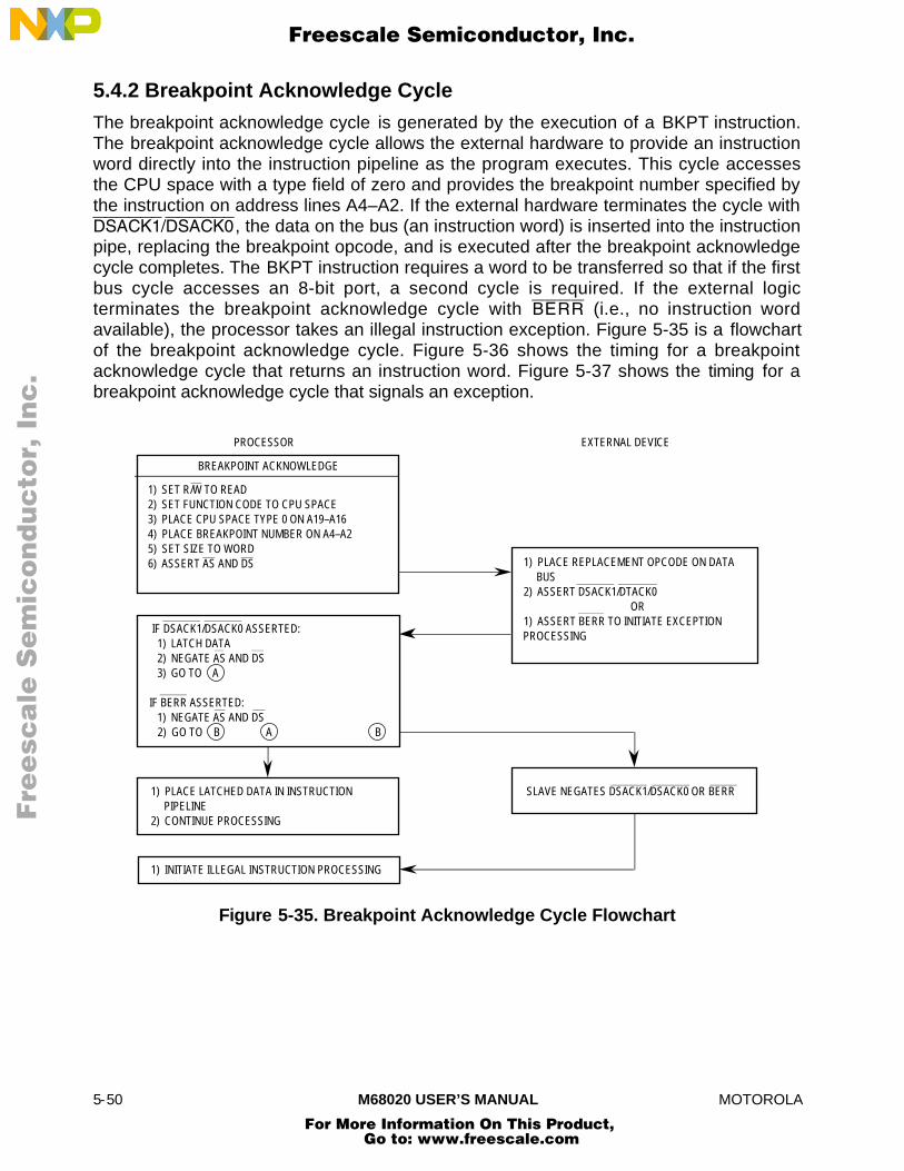
5-50 M68020 USER’S MANUAL MOTOROLA
5.4.2 Breakpoint Acknowledge Cycle
The breakpoint acknowledge cycle is generated by the execution of a BKPT instruction.The breakpoint acknowledge cycle allows the external hardware to provide an instructionword directly into the instruction pipeline as the program executes. This cycle accessesthe CPU space with a type field of zero and provides the breakpoint number specified bythe instruction on address lines A4–A2. If the external hardware terminates the cycle withDSACK1/DSACK0 , the data on the bus (an instruction word) is inserted into the instructionpipe, replacing the breakpoint opcode, and is executed after the breakpoint acknowledgecycle completes. The BKPT instruction requires a word to be transferred so that if the firstbus cycle accesses an 8-bit port, a second cycle is required. If the external logicterminates the breakpoint acknowledge cycle with BERR (i.e., no instruction wordavailable), the processor takes an illegal instruction exception. Figure 5-35 is a flowchartof the breakpoint acknowledge cycle. Figure 5-36 shows the timing for a breakpointacknowledge cycle that returns an instruction word. Figure 5-37 shows the timing for abreakpoint acknowledge cycle that signals an exception.
1) PLACE REPLACEMENT OPCODE ON DATA BUS2) ASSERT DSACK1/DTACK0 OR1) ASSERT BERR TO INITIATE EXCEPTION PROCESSING
PROCESSOR
1) SET R/W TO READ2) SET FUNCTION CODE TO CPU SPACE3) PLACE CPU SPACE TYPE 0 ON A19–A16 4) PLACE BREAKPOINT NUMBER ON A4–A25) SET SIZE TO WORD6) ASSERT AS AND DS
BREAKPOINT ACKNOWLEDGE
1) PLACE LATCHED DATA IN INSTRUCTION PIPELINE2) CONTINUE PROCESSING
1) INITIATE ILLEGAL INSTRUCTION PROCESSING
SLAVE NEGATES DSACK1/DSACK0 OR BERR
EXTERNAL DEVICE
IF DSACK1/DSACK0 ASSERTED: 1) LATCH DATA 2) NEGATE AS AND DS 3) GO TO A
IF BERR ASSERTED: 1) NEGATE AS AND DS 2) GO TO B A B
Figure 5-35. Breakpoint Acknowledge Cycle Flowchart
Fre
esc
ale
Se
mic
on
du
cto
r, I
Freescale Semiconductor, Inc.
For More Information On This Product, Go to: www.freescale.com
nc
...
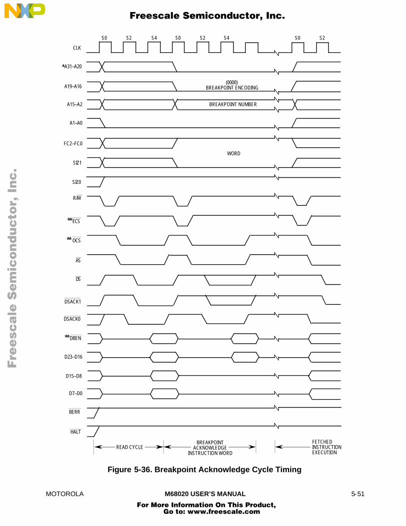
MOTOROLA M68020 USER’S MANUAL 5-51
BREAKPOINTACKNOWLEDGE
INSTRUCTION WORDFETCH
READ CYCLE
CLK
A31–A20
A19–A16
A15–A2
FC2–FC0
SIZ1
R/W
ECS
OCS
AS
DS
DSACK0
DBEN
D23–D16
SIZ0
DSACK1
S0 S2 S4 S0 S2 S4 S0 S2
D7–D0
D15–D8
BREAKPOINT NUMBER
WORD
FETCHED INSTRUCTIONEXECUTION
(0000)BREAKPOINT ENCODING
A1–A0
HALT
BERR
**
**
**
*
Figure 5-36. Breakpoint Acknowledge Cycle Timing
Fre
esc
ale
Se
mic
on
du
cto
r, I
Freescale Semiconductor, Inc.
For More Information On This Product, Go to: www.freescale.com
nc
...

5-52 M68020 USER’S MANUAL MOTOROLA
CLK
A31–A0
FC2–FC0
R/W
ECS
OCS
AS
DS
DSACK0
DBEN
SIZ1–SIZ0
DSACK1
S0 S2 S4 S0 S2
HALT
Sw Sw Sw S4
D31–D0
BERR
READ WITH BERR ASSERTED INTERNALPROCESSING STACK WRITE
**
**
**
*
* For the MC68EC020, A23–A0.This signal does not apply to the MC68EC020.**
Figure 5-37. Breakpoint Acknowledge Cycle Timing (Exception Signaled)
Fre
esc
ale
Se
mic
on
du
cto
r, I
Freescale Semiconductor, Inc.
For More Information On This Product, Go to: www.freescale.com
nc
...

MOTOROLA M68020 USER’S MANUAL 5-53
5.4.3 Coprocessor Communication Cycles
The MC68020/EC020 coprocessor interface provides instruction-oriented communicationbetween the processor and as many as eight coprocessors. Coprocessor accesses usethe MC68020/EC020 bus protocol except that the address bus supplies accessinformation rather than a 32-bit address. The CPU space type field (A19–A16) for acoprocessor operation is 0010. A15–A13 contain the coprocessor identification number(CpID), and A5–A0 specify the coprocessor interface register to be accessed. Thememory management unit of an MC68020/EC020 system is always identified by a CpID ofzero and has an extended register select field (A7–A0) in CPU space 0001 for use by theCALLM and RTM access level checking mechanism. Refer to Section 9 ApplicationsInformation for more details.
5.5 BUS EXCEPTION CONTROL CYCLES
The MC68020/EC020 bus architecture requires assertion of DSACK1/DSACK0 from anexternal device to signal that a bus cycle is complete. DSACK1/DSACK0 or AVEC is notasserted if:
• The external device does not respond,
• No interrupt vector is provided, or
• Various other application-dependent errors occur.
External circuitry can assert B E R R when no device responds by assertingDSACK1/DSACK0 or AVEC within an appropriate period of time after the processorasserts AS. Assertion of BERR allows the cycle to terminate and the processor to enterexception processing for the error condition.
HALT is also used for bus exception control. HALT can be asserted by an external devicefor debugging purposes to cause single bus cycle operation or can be asserted incombination with BERR to cause a retry of a bus cycle in error.
To properly control termination of a bus cycle for a retry or a bus error condition,DSACK1/DSACK0 , BERR, and HALT can be asserted and negated with the rising edge ofthe MC68020/EC020 clock. This procedure ensures that when two signals are assertedsimultaneously, the required setup time (#47A) and hold time (#47B) for both of them ismet for the same falling edge of the processor clock. (Refer to Section 10 ElectricalCharacteristics for timing requirements.) This or some equivalent precaution should bedesigned into the external circuitry that provides these signals.
Fre
esc
ale
Se
mic
on
du
cto
r, I
Freescale Semiconductor, Inc.
For More Information On This Product, Go to: www.freescale.com
nc
...
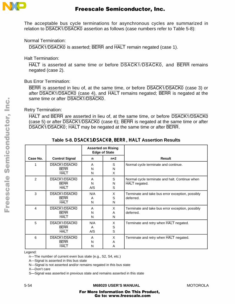
5-54 M68020 USER’S MANUAL MOTOROLA
The acceptable bus cycle terminations for asynchronous cycles are summarized inrelation to DSACK1/DSACK0 assertion as follows (case numbers refer to Table 5-8):
Normal Termination:DSACK1/DSACK0 is asserted; BERR and HALT remain negated (case 1).
Halt Termination:HALT is asserted at same time or before DSACK1/DSACK0, and BERR remainsnegated (case 2).
Bus Error Termination:BERR is asserted in lieu of, at the same time, or before DSACK1/DSACK0 (case 3) orafter DSACK1/DSACK0 (case 4), and HALT remains negated; BERR is negated at thesame time or after DSACK1/DSACK0 .
Retry Termination:HALT and BERR are asserted in lieu of, at the same time, or before DSACK1/DSACK0
(case 5) or after DSACK1/DSACK0 (case 6); BERR is negated at the same time or afterDSACK1/DSACK0 ; HALT may be negated at the same time or after BERR.
Table 5-8. DSACK1/DSACK0 , BERR, HALT Assertion Results
Asserted on RisingEdge of State
Case No. Control Signal n n+2 Result
1 DSACK1/DSACK0
BERR
HALT
ANN
SNX
Normal cycle terminate and continue.
2 DSACK1/DSACK0
BERR
HALT
AN
A/S
SNS
Normal cycle terminate and halt. Continue whenHALT negated.
3 DSACK1/DSACK0
BERR
HALT
N/AAN
XSN
Terminate and take bus error exception, possiblydeferred.
4 DSACK1/DSACK0
BERR
HALT
ANN
XAN
Terminate and take bus error exception, possiblydeferred.
5 DSACK1/DSACK0
BERR
HALT
N/AA
A/S
XSS
Terminate and retry when HALT negated.
6 DSACK1/DSACK0
BERR
HALT
ANN
XAA
Terminate and retry when HALT negated.
Legend:n—The number of current even bus state (e.g., S2, S4, etc.)A—Signal is asserted in this bus stateN—Signal is not asserted and/or remains negated in this bus stateX—Don’t careS—Signal was asserted in previous state and remains asserted in this state
Fre
esc
ale
Se
mic
on
du
cto
r, I
Freescale Semiconductor, Inc.
For More Information On This Product, Go to: www.freescale.com
nc
...

MOTOROLA M68020 USER’S MANUAL 5-55
Table 5-8 lists various combinations of control signal sequences and the resulting buscycle terminations. To ensure predictable operation, BERR and HALT should be negatedaccording to parameters #28 and #57 in Section 10 Electrical Characteristics.DSACK1/DSACK0 , BERR, and HALT may be negated after AS. If DSACK1/DSACK0 orBERR remain asserted into S2 of the next bus cycle, that cycle may be terminatedprematurely.
Example A:A system uses a watchdog timer to terminate accesses to an unpopulated addressspace. The timer asserts BERR after timeout (case 3).
Example B:A system uses error detection and correction on RAM contents. The designer may:
1. Delay DSACK1/DSACK0 assertion until data is verified and assert BERR andHALT simultaneously to indicate to the processor to automatically retry the errorcycle (case 5) or, if data is valid, assert DSACK1/DSACK0 (case 1).
2. Delay DSACK1/DSACK0 assertion until data is verified and assert BERR with orwithout DSACK1/DSACK0 if data is in error (case 3). This configuration initiatesexception processing for software handling of the condition.
3. Assert DSACK1/DSACK0 prior to data verification. If data is invalid, BERR isasserted on the next clock cycle (case 4). This configuration initiates exceptionprocessing for software handling of the condition.
4. Assert DSACK1/DSACK0 prior to data verification; if data is invalid, assert BERRand HALT on the next clock cycle (case 6). The memory controller can thencorrect the RAM prior to or during the automatic retry.
5.5.1 Bus Errors
The BERR signal can be used to abort the bus cycle and the instruction being executed.BERR takes precedence over DSACK1/DSACK0, provided it meets the timing constraintsdescribed in Section 10 Electrical Characteristics. If BERR does not meet theseconstraints, it may cause unpredictable operation of the MC68020/EC020. If BERR
remains asserted into the next bus cycle, it may cause incorrect operation of that cycle.
When BERR is issued to terminate a bus cycle, the MC68020/EC020 may enter exceptionprocessing immediately following the bus cycle, or it may defer processing the exception.The instruction prefetch mechanism requests instruction words from the bus controller andthe instruction cache before it is ready to execute them. If a bus error occurs on aninstruction fetch, the processor does not take the exception until it attempts to use thatinstruction word. Should an intervening instruction cause a branch or should a task switchoccur, the bus error exception does not occur.
Fre
esc
ale
Se
mic
on
du
cto
r, I
Freescale Semiconductor, Inc.
For More Information On This Product, Go to: www.freescale.com
nc
...
5-56 M68020 USER’S MANUAL MOTOROLA
BERR is recognized during a bus cycle in any of the following cases:1. DSACK1/DSACK0 and HALT are negated and BERR is asserted.
2. HALT and BERR are negated and DSACK1/DSACK0 is asserted. BERR is thenasserted within one clock cycle (HALT remains negated).
3. BERR and HALT are asserted (see 5.5.2 Retry Operation).
When the processor recognizes a bus error condition, it terminates the current bus cyclein the normal way. Figure 5-38 shows the timing of a bus error for the case in whichDSACK1/DSACK0 is not asserted. Figure 5-39 shows the timing for a bus error for thecase in which BERR is asserted after DSACK1/DSACK0 . Exceptions are taken in bothcases. (Refer to Section 6 Exception Processing for details of bus error exceptionprocessing.) When BERR is asserted during a read cycle that supplies an instruction tothe on-chip cache, the instruction in the cache is marked invalid.
When BERR is asserted after DSACK1/DSACK0 , BERR must be asserted withinparameter #48 (refer to Section 10 Electrical Characteristics) for purely asynchronousoperation, or it must be asserted and remain stable during the sample window, defined byparameters #27A and #47B, around the next falling edge of the clock afterDSACK1/DSACK0 is recognized. If BERR is not stable at this time, the processor mayexhibit erratic behavior. In this case, data may be present on the bus, but may not bevalid. This sequence may be used by systems that have memory error detection andcorrection logic and by external cache memories.
5.5.2 Retry Operation
When BERR and HALT are asserted simultaneously by an external device during a buscycle, the processor enters the retry sequence. A delayed retry similar to the delayedBERR signal described previously can also occur.
The processor terminates the bus cycle, negates the control signals (AS, DS, R/W, SIZ1,SIZ0, RMC, and, for the MC68020 only, ECS and OCS), and does not begin another buscycle until the BERR and HALT signals have been negated by external logic. After asynchronization delay, the processor retries the previous cycle using the same accessinformation (address, function code, size, etc.) The BERR signal should be negated beforeS2 of the read cycle to ensure correct operation of the retried cycle. Figure 5-40 shows alate retry operation of a cycle.
The processor retries any read or write cycle of a read-modify-write operation separately;RMC remains asserted during the entire retry sequence.
Asserting BR along with BERR and HALT provides a relinquish and retry operation. TheMC68020/EC020 does not relinquish the bus during a read-modify-write operation. Anydevice that requires the processor to give up the bus and retry a bus cycle during a read-modify-write cycle must assert BERR and BR only (HALT must not be included). The buserror handler software should examine the read-modify-write bit in the special status word(refer to Section 6 Exception Processing) and take the appropriate action to resolve thistype of fault when it occurs.
Fre
esc
ale
Se
mic
on
du
cto
r, I
Freescale Semiconductor, Inc.
For More Information On This Product, Go to: www.freescale.com
nc
...

MOTOROLA M68020 USER’S MANUAL 5-57
BREAKPOINTACKNOWLEDGE
BUS ERRORFETCH
READ CYCLE
CLK
A31–A20
A19–A16
A15–A2
FC2–FC0
SIZ1
R/W
ECS
OCS
AS
DS
DSACK0
DBEN
D23–D16
SIZ0
DSACK1
S0 S2 S4 S0 S2 S4 S0 S2
D7–D0
D15–D8
BREAKPOINT NUMBER
WORD
EXCEPTIONSTACKING
(0000)BREAKPOINT ENCODING
A1–A0
HALT
BERR
CPU SPACE
D31–D24
**
**
**
*
* For the MC68EC020, A23–A20.This signal does not apply to the MC68EC020.**
Figure 5-38. Bus Error without DSACK1/DSACK0
Fre
esc
ale
Se
mic
on
du
cto
r, I
Freescale Semiconductor, Inc.
For More Information On This Product, Go to: www.freescale.com
nc
...

5-58 M68020 USER’S MANUAL MOTOROLA
CLK
A31–A0
FC2–FC0
R/W
ECS
OCS
AS
DS
DSACK0
DBEN
D31–D0
IPL2–IPL0
DSACK1
S0 S2 Sw S4 S0 S2Sw S4
SIZ1–SIZ0
BERR
HALT
WRITE WITH BERR ASSERTED INTERNALPROCESSING
STACK WRITE
**
**
**
*
* For the MC68EC020, A23–A0.This signal does not apply to the MC68EC020.**
Figure 5-39. Late Bus Error with DSACK1/DSACK0
Fre
esc
ale
Se
mic
on
du
cto
r, I
Freescale Semiconductor, Inc.
For More Information On This Product, Go to: www.freescale.com
nc
...

MOTOROLA M68020 USER’S MANUAL 5-59
A31–A0
FC2–FC0
ECS
OCS
AS
DS
DSACK1
CLK
S0 S4 S0
SIZ1–SIZ0
R/W
DSACK0
D31–D0DATA BUS NOT DRIVEN
BERR
HALT
WRITE CYCLE RETRY SIGNALED HALT RETRY CYCLE
S2 Sw S2 S4
**
**
*
* For the MC68EC020, A23–A0.This signal does not apply to the MC68EC020.**
Figure 5-40. Late Retry
Fre
esc
ale
Se
mic
on
du
cto
r, I
Freescale Semiconductor, Inc.
For More Information On This Product, Go to: www.freescale.com
nc
...
5-60 M68020 USER’S MANUAL MOTOROLA
5.5.3 Halt Operation
When HALT is asserted and BERR is not asserted, the MC68020/EC020 halts externalbus activity at the next bus cycle boundary. HALT by itself does not terminate a bus cycle.Negating and reasserting HALT in accordance with the correct timing requirementsprovides a single-step (bus cycle to bus cycle) operation. The HALT signal affects externalbus cycles only; thus, a program that resides in the instruction cache and does not requireuse of the external bus may continue executing unaffected by HALT.
The single-cycle mode allows the user to proceed through (and debug) external processoroperations, one bus cycle at a time. Figure 5-41 shows the timing requirements for asingle-cycle operation. Since the occurrence of a bus error while HALT is asserted causesa retry operation, the user must anticipate retry cycles while debugging in the single-cyclemode. The single-step operation and the software trace capability allow the systemdebugger to trace single bus cycles, single instructions, or changes in program flow.These processor capabilities, along with a software debugging package, give completedebugging flexibility.
When the processor completes a bus cycle with the HALT signal asserted, the data bus isplaced in the high-impedance state, and the bus control signals (AS, DS, and, for theMC68020 only, ECS and OCS) are negated (not placed in the high-impedance state);A31–A0 for the MC68020 or A23–A0 for the MC68EC020, FC2–FC0, SIZ1, SIZ0, andR/W remain in the same state. The halt operation has no effect on bus arbitration (refer to5.7 Bus Arbitration). When bus arbitration occurs while the MC68020/EC020 is halted,the address and control signals (A31–A0, FC2–FC0, SIZ1, SIZ0, R/W, AS, DS, and, forthe MC68020 only, ECS and OCS) are also placed in the high-impedance state. Once busmastership is returned to the MC68020/EC020, if HALT is still asserted, A31–A0 for theMC68020 or A23–A0 for the MC68EC020, FC2–FC0, SIZ1, SIZ0, and R/W are againdriven to their previous states. The MC68020/EC020 does not service interrupt requestswhile it is halted (although the MC68020 may assert the IPEND signal as appropriate).
5.5.4 Double Bus Fault
When a bus error or an address error occurs during the exception processing sequencefor a previous bus error, a previous address error, or a reset exception, a double bus faultoccurs. For example, the processor attempts to stack several words containinginformation about the state of the machine while processing a bus error exception. If a buserror exception occurs during the stacking operation, the second error is considered adouble bus fault. When a double bus fault occurs, the processor halts and asserts HALT.Only an external reset operation can restart a halted processor. However, bus arbitrationcan still occur (refer to 5.7 Bus Arbitration).
A second bus error or address error that occurs after exception processing has completed(during the execution of the exception handler routine or later) does not cause a doublebus fault. A bus cycle that is retried does not constitute a bus error or contribute to adouble bus fault. The processor continues to retry the same bus cycle as long as theexternal hardware requests it.
Fre
esc
ale
Se
mic
on
du
cto
r, I
Freescale Semiconductor, Inc.
For More Information On This Product, Go to: www.freescale.com
nc
...

MOTOROLA M68020 USER’S MANUAL 5-61
CLK
A31–A0
FC2–FC0
R/W
ECS
OCS
AS
DS
DSACK0
DBEN
DSACK1
S0 S2 S0
BERR
HALT
S4 S2
SIZ1–SIZ0
S4
D31–D0
**
**
**
*
READHALT
(BUS ARBITRATION PERMITTED
WHILE THE PROCESSORIS HALTED)
READ
* For the MC68EC020, A23–A0.This signal does not apply to the MC68EC020.**
Figure 5-41. Halt Operation Timing
Fre
esc
ale
Se
mic
on
du
cto
r, I
Freescale Semiconductor, Inc.
For More Information On This Product, Go to: www.freescale.com
nc
...

5-62 M68020 USER’S MANUAL MOTOROLA
5.6 BUS SYNCHRONIZATION
The MC68020/EC020 overlaps instruction execution—that is, during bus activity for oneinstruction, instructions that do not use the external bus can be executed. Due to theindependent operation of the on-chip cache relative to the operation of the bus controller,many subsequent instructions can be executed, resulting in seemingly nonsequentialinstruction execution. When this is not desired and the system depends on sequentialexecution following bus activity, the NOP instruction can be used. The NOP instructionforces instruction and bus synchronization by freezing instruction execution until allpending bus cycles have completed.
An example of the use of the NOP instruction for this purpose is the case of a writeoperation of control information to an external register in which the external hardwareattempts to control program execution based on the data that is written with theconditional assertion of BERR. Since the MC68020/EC020 cannot process the bus erroruntil the end of the bus cycle, the external hardware has not successfully interruptedprogram execution. To prevent a subsequent instruction from executing until the externalcycle completes, the NOP instruction can be inserted after the instruction causing thewrite. In this case, bus error exception processing proceeds immediately after the writeand before subsequent instructions are executed. This is an irregular situation, and theuse of the NOP instruction for this purpose is not required by most systems.
5.7 BUS ARBITRATION
The bus design of the MC68020/EC020 provides for a single bus master at any one time:either the processor or an external device. One or more of the external devices on the buscan have the capability of becoming bus master. Bus arbitration is the protocol by whichan external device becomes bus master; the bus controller in the MC68020/EC020manages the bus arbitration signals so that the processor has the lowest priority.
Bus arbitration differs in the MC68020 and MC68EC020 due to the absence of BGACK inthe MC68EC020. Because of this difference, bus arbitration of the MC68020 andMC68EC020 is discussed separately.
External devices that need to obtain the bus must assert the bus arbitration signals in thesequences described in 5.7.1 MC68020 Bus Arbitration or 5.7.2 MC68EC020 BusArbitration. Systems having several devices that can become bus master requireexternal circuitry to assign priorities to the devices, so that when two or more externaldevices attempt to become bus master at the same time, the one having the highestpriority becomes bus master first.
Fre
esc
ale
Se
mic
on
du
cto
r, I
Freescale Semiconductor, Inc.
For More Information On This Product, Go to: www.freescale.com
nc
...
MOTOROLA M68020 USER’S MANUAL 5-63
5.7.1 MC68020 Bus Arbitration
The sequence of the MC68020 bus arbitration protocol is as follows:1. An external device asserts the BR signal.
2. The processor asserts the BG signal to indicate that the bus will become available atthe end of the current bus cycle.
3. The external device asserts the BGACK signal to indicate that it has assumed busmastership.
BR may be issued any time during a bus cycle or between cycles. BG is asserted inresponse to BR; it is usually asserted as soon as BR has been synchronized andrecognized, except when the MC68020 has made an internal decision to execute a buscycle. Then, the assertion of BG is deferred until the bus cycle has begun. Additionally, BG
is not asserted until the end of a read-modify-write operation (when RMC is negated) inresponse to a BR signal. When the requesting device receives BG and more than oneexternal device can be bus master, the requesting device should begin whateverarbitration is required. The external device asserts BGACK when it assumes busmastership, and maintains BGACK during the entire bus cycle (or cycles) for which it isbus master. The following conditions must be met for an external device to assumemastership of the bus through the normal bus arbitration procedure:
• The external device must have received BG through the arbitration process.
• AS must be negated, indicating that no bus cycle is in progress, and the externaldevice must ensure that all appropriate processor signals have been placed in thehigh-impedance state (by observing specification #7 in Section 10 ElectricalSpecifications).
• The termination signal (DSACK1/DSACK0) for the most recent cycle must have beennegated, indicating that external devices are off the bus (optional, refer to 5.7.1.3 BusGrant Acknowledge (MC68020)).
• BGACK must be inactive, indicating that no other bus master has claimed ownershipof the bus.
Figure 5-42 is a flowchart of MC68020 bus arbitration for a single device. Figure 5-43 is atiming diagram for the same operation. This technique allows processing of bus requestsduring data transfer cycles.
Fre
esc
ale
Se
mic
on
du
cto
r, I
Freescale Semiconductor, Inc.
For More Information On This Product, Go to: www.freescale.com
nc
...

5-64 M68020 USER’S MANUAL MOTOROLA
1) ASSERT BG
GRANT BUS ARBITRATION
TERMINATE ARBITRATION
1) NEGATE BG AND WAIT FOR BGACK TO BE NEGATED
RE-ARBITRATE OR RESUME PROCESSOR OPERATION
REQUEST THE BUS
1) ASSERT BR
REQUESTING DEVICEPROCESSOR
ACKNOWLEDGE BUS MASTERSHIP
1) EXTERNAL ARBITRATION DETERMINES NEXT BUS MASTER2) NEXT BUS MASTER WAITS FOR CURRENT CYCLE TO COMPLETE3) NEXT BUS MASTER ASSERTS BGACKTO BECOME NEW MASTER4) BUS MASTER NEGATES BR
OPERATE AS BUS MASTER
RELEASE BUS MASTERSHIP
1) PERFORM DATA TRANSFERS (READ AND WRITE CYCLES)
1) NEGATE BGACK
Figure 5-42. MC68020 Bus Arbitration Flowchart for Single Request
The timing diagram (see Figure 5-43) shows that BR is negated at the time that BGACK isasserted. This type of operation applies to a system consisting of the processor and onedevice capable of bus mastership. In a system having a number of devices capable of busmastership, the BR line from each device can be wire-ORed to the processor. In such asystem, more than one bus request can be asserted simultaneously.
The timing diagram in Figure 5-43 shows that BG is negated a few clock cycles after thetransition of BGACK. However, if bus requests are still pending after the negation of BG,the processor asserts another BG within a few clock cycles after it was negated. Thisadditional assertion of BG allows external arbitration circuitry to select the next bus masterbefore the current bus master has finished with the bus. The following paragraphs provideadditional information about the three steps in the arbitration process.
Bus arbitration requests are recognized during normal processing, RESET assertion,HALT assertion, and when the processor has halted due to a double bus fault.
Fre
esc
ale
Se
mic
on
du
cto
r, I
Freescale Semiconductor, Inc.
For More Information On This Product, Go to: www.freescale.com
nc
...

MOTOROLA M68020 USER’S MANUAL 5-65
A31–A0
FC2–FC0
ECS
OCS
AS
DS
DSACK1
CLK
S0 S4 S0
SIZ1–SIZ0
R/W
DSACK0
DBEN
S2 S2
BGACK
BG
BR
D31–D0
PROCESSOR DMA DEVICE PROCESSOR
Figure 5-43. MC68020 Bus Arbitration Operation Timing for Single Request
Fre
esc
ale
Se
mic
on
du
cto
r, I
Freescale Semiconductor, Inc.
For More Information On This Product, Go to: www.freescale.com
nc
...

5-66 M68020 USER’S MANUAL MOTOROLA
5.7.1.1 BUS REQUEST (MC68020). External devices capable of becoming bus mastersrequest the bus by asserting BR. BR can be a wire-ORed signal (although it need not beconstructed from open-collector devices) that indicates to the processor that someexternal device requires control of the bus. The processor is at a lower bus priority levelthan the external device and relinquishes the bus after it has completed the current buscycle (if one has started).
If no BGACK is received while BR is asserted, the processor remains bus master once BR
is negated. This prevents unnecessary interference with ordinary processing if thearbitration circuitry inadvertently responds to noise or if an external device determines thatit no longer requires use of the bus before it has been granted mastership.
5.7.1.2 BUS GRANT (MC68020). The processor asserts BG as soon as possible afterreceipt of the bus request. BG assertion immediately follows internal synchronizationexcept during a read-modify-write cycle or follows an internal decision to execute a buscycle. During a read-modify-write cycle, the processor does not assert BG until the entireoperation has completed. RMC is asserted to indicate that the bus is locked. In the case ofan internal decision to execute another bus cycle, BG is deferred until the bus cycle hasbegun.
BG may be routed through a daisy-chained network or through a specific priority-encodednetwork. The processor allows any type of external arbitration that follows the protocol.
5.7.1.3 BUS GRANT ACKNOWLEDGE (MC68020). Upon receiving BG, the requestingdevice waits until AS, DSACK1/DSACK0 , and BGACK are negated before asserting itsown BGACK. The negation of AS indicates that the previous master releases the bus afterspecification #7 (refer to Section 10 Electrical Characteristics). The negation ofDSACK1/DSACK0 indicates that the previous slave has completed its cycle with theprevious master. Note that in some applications, DSACK1/DSACK0 might not be used inthis way.
General-purpose devices are connected to be dependent only on AS. When BGACK isasserted, the device is the bus master until it negates BGACK. BGACK should not benegated until all bus cycles required by the alternate bus master have been completed.Bus mastership terminates at the negation of BGACK. The BR from the granted deviceshould be negated after BGACK is asserted. If another BR is still pending after theassertion of BGACK, another BG is asserted within a few clocks of the negation of the thefirst BG, as described in 5.7.1.4 Bus Arbitration Control (MC68020). Note that theprocessor does not perform any external bus cycles before it reasserts BG in this case.
Fre
esc
ale
Se
mic
on
du
cto
r, I
Freescale Semiconductor, Inc.
For More Information On This Product, Go to: www.freescale.com
nc
...
MOTOROLA M68020 USER’S MANUAL 5-67
5.7.1.4 BUS ARBITRATION CONTROL (MC68020). The bus arbitration control unit in theMC68020 is implemented with a finite state machine. As discussed previously, allasynchronous inputs to the MC68020 are internally synchronized in a maximum of twocycles of the processor clock.
As shown in Figure 5-44, input signals labeled R and A are internally synchronizedversions of the BR and BGACK signals, respectively. The BG output is labeled G, and theinternal high-impedance control signal is labeled T. If T is true, the address, data, andcontrol buses are placed in the high-impedance state after the next rising edge followingthe negation of AS and RMC . All signals are shown in positive logic (active high),regardless of their true active voltage level.
GT
GT
GT
GT
GT
GT
GT
RA
RA
XX
RARA
RA
XX
RX
RA
XA
RA
RX
XA
RA
STATE 1
STATE 0
STATE 4
STATE 5
STATE 6
STATE 2
STATE 3
XX
R—BUS REQUESTA—BUS GRANT ACKNOWLEDGEG—BUS GRANTT—THREE-STATE CONTROL TO BUS CONTROL LOGICX—DON'T CARE
NOTE: The BG output will not be asserted while RMC is asserted.
Figure 5-44. MC68020 Bus Arbitration State Diagram
Fre
esc
ale
Se
mic
on
du
cto
r, I
Freescale Semiconductor, Inc.
For More Information On This Product, Go to: www.freescale.com
nc
...
5-68 M68020 USER’S MANUAL MOTOROLA
State changes occur on the next rising edge of the clock after the internal signal isrecognized as valid. The BG signal transitions on the falling edge of the clock after a stateis reached during which G changes. The bus control signals (controlled by T) are drivenby the processor immediately following a state change when bus mastership is returned tothe MC68020.
State 0, at the top center of the diagram, in which both G and T are negated, is the stateof the bus arbiter while the processor is bus master. Request R and acknowledge A keepthe arbiter in state 0 as long as they are both negated. When a request R is received, bothgrant G and signal T are asserted (in state 1 at the top left). The next clock causes achange to state 2, at the lower left, in which G and T are held. The bus arbiter remains inthat state until acknowledge A is asserted or request R is negated. Once either occurs, thearbiter changes to the center state, state 3, and negates grant G. The next clock takes thearbiter to state 4, at the upper right, in which grant G remains negated and signal Tremains asserted. With acknowledge A asserted, the arbiter remains in state 4 until A isnegated or request R is again asserted. When A is negated, the arbiter returns to theoriginal state, state 0, and negates signal T. This sequence of states follows the normalsequence of signals for relinquishing the bus to an external bus master. Other states applyto other possible sequences of combinations of R and A.
The MC68020 does not allow arbitration of the external bus during the read-modify-writesequence. For the duration of this sequence, the MC68020 ignores the BR input. Ifmastership of the MC68020 bus is required during a read-modify-write operation, BERR
must be used to abort the read-modify-write sequence. The bus arbitration sequencewhile the bus is inactive (i.e., executing internal operations such as a multiply instruction)is shown in Figure 5-45.
Fre
esc
ale
Se
mic
on
du
cto
r, I
Freescale Semiconductor, Inc.
For More Information On This Product, Go to: www.freescale.com
nc
...

MOTOROLA M68020 USER’S MANUAL 5-69
A31–A0
FC2–FC0
ECS
OCS
AS
DS
DSACK1
CLK
S4 S0
SIZ1–SIZ0
R/W
DSACK0
DBEN
BGACK
BG
BR
D31–D0
PROCESSOR PROCESSORALTERNATE MASTERBUS INACTIVE
(ARBITRATION PERMITTED WHILE THE PROCESSOR IS
INACTIVE OR HALTED)
Figure 5-45. MC68020 Bus Arbitration Operation Timing—Bus Inactive
Fre
esc
ale
Se
mic
on
du
cto
r, I
Freescale Semiconductor, Inc.
For More Information On This Product, Go to: www.freescale.com
nc
...
5-70 M68020 USER’S MANUAL MOTOROLA
5.7.2 MC68EC020 Bus Arbitration
The sequence of the MC68EC020 bus arbitration protocol is as follows:1. An external device asserts the BR signal.
2. The processor asserts the BG signal to indicate that the bus will become available atthe end of the current bus cycle.
3. The external device asserts the BR signal throughout its bus mastership.
BR may be issued any time during a bus cycle or between cycles. BG is asserted inresponse to BR; it is usually asserted as soon as BR has been synchronized andrecognized, except when the MC68020 has made an internal decision to execute a buscycle. Then, the assertion of BG is deferred until the bus cycle has begun. Additionally, BG
is not asserted until the end of a read-modify-write operation (when RMC is negated) inresponse to a BR signal. When the requesting device receives BG and more than oneexternal device can be bus master, the requesting device should begin whateverarbitration is required. The external device continues to assert BR when it assumes busmastership, and maintains BR during the entire bus cycle (or cycles) for which it is busmaster. The following conditions must be met for an external device to assume mastershipof the bus through the normal bus arbitration procedure:
• The external device must have received BG through the arbitration process.
• AS must be negated, indicating that no bus cycle is in progress, and the externaldevice must ensure that all appropriate processor signals have been placed in thehigh-impedance state (by observing specification #7 in Section 10 ElectricalSpecifications).
• The termination signal (DSACK1/DSACK0) for the most recent cycle must have beennegated, indicating that external devices are off the bus.
• No other bus master has claimed ownership of the bus.
Figure 5-46 is a flowchart of MC68EC020 bus arbitration for a single device. Figure 5-47 isa timing diagram for the same operation. This technique allows processing of busrequests during data transfer cycles.
Bus arbitration requests are recognized during normal processing, RESET assertion,HALT assertion, and when the processor has halted due to a double bus fault.
Fre
esc
ale
Se
mic
on
du
cto
r, I
Freescale Semiconductor, Inc.
For More Information On This Product, Go to: www.freescale.com
nc
...

MOTOROLA M68020 USER’S MANUAL 5-71
1) ASSERT BG
GRANT BUS ARBITRATION
RE-ARBITRATE OR RESUME PROCESSOR OPERATION
REQUEST THE BUS
1) ASSERT BR
REQUESTING DEVICEPROCESSOR
ACKNOWLEDGE BUS MASTERSHIP
1) EXTERNAL ARBITRATION DETERMINES NEXT BUS MASTER2) NEXT BUS MASTER WAITS FOR CURRENT CYCLE TO COMPLETE3) PERFORM DATA TRANSFERS (READ AND WRITE CYCLES)
OPERATE AS BUS MASTER
RELEASE BUS MASTERSHIP
1) NEGATE BR
Figure 5-46. MC68EC020 Bus Arbitration Flowchart for Single Request
5.7.2.1 BUS REQUEST (MC68EC020). External devices capable of becoming busmasters request the bus by asserting BR. BR can be a wire-ORed signal (although it neednot be constructed from open-collector devices) that indicates to the processor that someexternal device requires control of the bus. The processor is at a lower bus priority levelthan the external device and relinquishes the bus after it has completed the current buscycle (if one has started). BR remains asserted throughout the external device’s busmastership.
5.7.2.2 BUS GRANT (MC68EC020). The processor asserts BG as soon as possible afterreceipt of the bus request. BG assertion immediately follows internal synchronizationexcept during a read-modify-write cycle or follows an internal decision to execute a buscycle. During a read-modify-write cycle, the processor does not assert BG until the entireoperation has completed. RMC is asserted to indicate that the bus is locked. In the case ofan internal decision to execute another bus cycle, BG is deferred until the bus cycle hasbegun.
BG may be routed through a daisy-chained network or through a specific priority-encodednetwork. The processor allows any type of external arbitration that follows the protocol.
Fre
esc
ale
Se
mic
on
du
cto
r, I
Freescale Semiconductor, Inc.
For More Information On This Product, Go to: www.freescale.com
nc
...

5-72 M68020 USER’S MANUAL MOTOROLA
A23–A0
FC2–FC0
AS
DS
DSACK1
CLK
S0 S4 S0
SIZ1–SIZ0
R/W
DSACK0
S2 S2
BG
BR
D31–D0
PROCESSOR DMA DEVICE PROCESSOR
Figure 5-47. MC68EC020 Bus Arbitration Operation Timing for Single Request
Fre
esc
ale
Se
mic
on
du
cto
r, I
Freescale Semiconductor, Inc.
For More Information On This Product, Go to: www.freescale.com
nc
...

MOTOROLA M68020 USER’S MANUAL 5-73
5.7.2.3 BUS ARBITRATION CONTROL (MC68EC020). The bus arbitration control unit inthe MC68EC020 is implemented with a finite state machine. As discussed previously, allasynchronous inputs to the MC68EC020 are internally synchronized in a maximum of twocycles of the processor clock.
As shown in Figure 5-48, the input signal labeled R is an internally synchronized versionof the BR signal. The BG output is labeled G, and the internal high-impedance controlsignal is labeled T. If T is true, the address, data, and control buses are placed in the high-impedance state after the next rising edge following the negation of AS and RMC. Allsignals are shown in positive logic (active high), regardless of their true active voltagelevel.
GT
GT
GTSTATE 3
GT
GT
GTSTATE 2
GT
STATE1
STATE 0
STATE 4
STATE 5
STATE 6
R—BUS REQUESTG—BUS GRANTT —THREE-STATE CONTROL TO BUS CONTROL LOGICX—DON'T CARE
R
R
R
R
X RX
R
RX
R
Figure 5-48. MC68EC020 Bus Arbitration State Diagram
Fre
esc
ale
Se
mic
on
du
cto
r, I
Freescale Semiconductor, Inc.
For More Information On This Product, Go to: www.freescale.com
nc
...
5-74 M68020 USER’S MANUAL MOTOROLA
State changes occur on the next rising edge of the clock after the internal signal isrecognized as valid. The BG signal transitions on the falling edge of the clock after a stateis reached during which G changes. The bus control signals (controlled by T) are drivenby the processor immediately following a state change when bus mastership is returned tothe MC68EC020.
State 0, at the top center of the diagram, in which both G and T are negated, is the stateof the bus arbiter while the processor is bus master. Request R keeps the arbiter in state 0as long as it is negated. When a request R is received, both grant G and signal T areasserted (in state 1 at the top left). The next clock causes a change to state 2, at the lowerleft, in which G and T are held. The bus arbiter remains in that state until request R isnegated. Then the arbiter changes to the center state, state 3, and negates grant G. Thenext clock takes the arbiter to state 4, at the upper right, in which grant G remains negatedand signal T remains asserted. The arbiter returns to the original state, state 0, andnegates signal T. This sequence of states follows the normal sequence of signals forrelinquishing the bus to an external bus master. Other states apply to other possiblesequences of R.
The MC68EC020 does not allow arbitration of the external bus during the read-modify-write sequence. For the duration of this sequence, the MC68EC020 ignores the BR input.If mastership of the MC68EC020 bus is required during a read-modify-write operation,BERR must be used to abort the read-modify-write sequence. The bus arbitrationsequence while the bus is inactive (i.e., executing internal operations such as a multiplyinstruction) is shown in Figure 5-49.
Fre
esc
ale
Se
mic
on
du
cto
r, I
Freescale Semiconductor, Inc.
For More Information On This Product, Go to: www.freescale.com
nc
...

MOTOROLA M68020 USER’S MANUAL 5-75
A23–A0
FC2–FC0
AS
DS
DSACK1
CLK
S4 S0
SIZ1–SIZ0
R/W
DSACK0
BG
BR
D31–D0
PROCESSOR PROCESSORALTERNATE MASTERBUS INACTIVE
(ARBITRATION PERMITTED WHILE THE PROCESSOR IS
INACTIVE OR HALTED)
Figure 5-49. MC68EC020 Bus Arbitration Operation Timing—Bus Inactive
The existing three-wire arbitration design (BR, BG, and BGACK) of some peripherals canbe converted to the MC68EC020 two-wire arbitration with the addition of an AND gate.Figure 5-50 shows the combination of BR and BGACK for a three-wire arbitration systemto BR of the MC68EC020 or BR and BG from an MC68EC020 to BG for a three-wirearbitration system. The speed of the AND gate must be faster than the time between theassertion of BGACK and the negation of BR by the alternate bus master. Figure 5-50assumes the alternate bus master does not assume bus mastership until the MC68EC020AS is negated and MC68EC020 BG is asserted.
Fre
esc
ale
Se
mic
on
du
cto
r, I
Freescale Semiconductor, Inc.
For More Information On This Product, Go to: www.freescale.com
nc
...
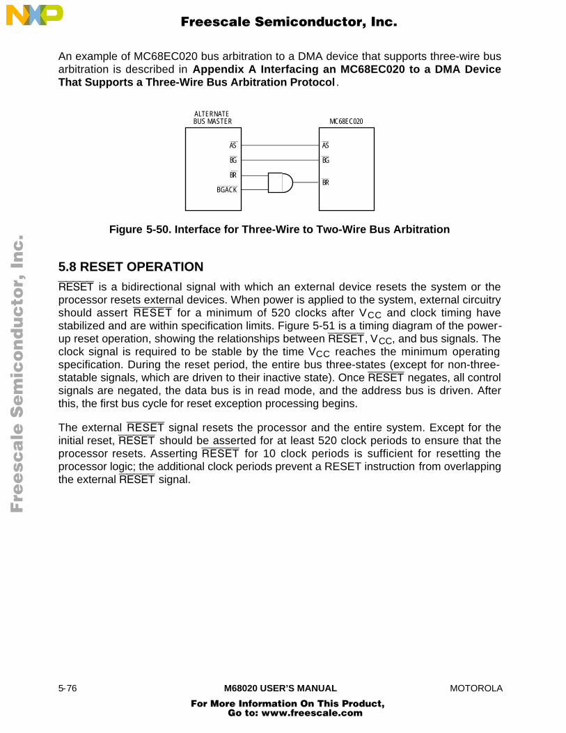
5-76 M68020 USER’S MANUAL MOTOROLA
An example of MC68EC020 bus arbitration to a DMA device that supports three-wire busarbitration is described in Appendix A Interfacing an MC68EC020 to a DMA DeviceThat Supports a Three-Wire Bus Arbitration Protocol .
AS
BG
BR
BGACK
ALTERNATE BUS MASTER
AS
BG
MC68EC020
BR
Figure 5-50. Interface for Three-Wire to Two-Wire Bus Arbitration
5.8 RESET OPERATION
RESET is a bidirectional signal with which an external device resets the system or theprocessor resets external devices. When power is applied to the system, external circuitryshould assert RESET for a minimum of 520 clocks after VCC and clock timing havestabilized and are within specification limits. Figure 5-51 is a timing diagram of the power-up reset operation, showing the relationships between RESET, VCC, and bus signals. Theclock signal is required to be stable by the time VCC reaches the minimum operatingspecification. During the reset period, the entire bus three-states (except for non-three-statable signals, which are driven to their inactive state). Once RESET negates, all controlsignals are negated, the data bus is in read mode, and the address bus is driven. Afterthis, the first bus cycle for reset exception processing begins.
The external RESET signal resets the processor and the entire system. Except for theinitial reset, RESET should be asserted for at least 520 clock periods to ensure that theprocessor resets. Asserting RESET for 10 clock periods is sufficient for resetting theprocessor logic; the additional clock periods prevent a RESET instruction from overlappingthe external RESET signal.
Fre
esc
ale
Se
mic
on
du
cto
r, I
Freescale Semiconductor, Inc.
For More Information On This Product, Go to: www.freescale.com
nc
...

MOTOROLA M68020 USER’S MANUAL 5-77
ISPREADSTARTS
ALL CONTROL SIGNALSNEGATED, DATA BUS INREAD MODE, ADDRESS
BUS DRIVEN
ENTIRE BUS THREE-STATED
BUS STATE UNKNOWN
t ≥ 520 CLOCKS
t < 4 CLOCKS
4 CLOCKS
CLK
+5 V
VCC
BUSCYCLES
RESET
Figure 5-51. Initial Reset Operation Timing
Resetting the processor causes any bus cycle in progress to terminate as ifDSACK1/DSACK0 or BERR had been asserted. In addition, the processor initializesregisters appropriately for a reset exception. Exception processing for a reset operation isdescribed in Section 6 Exception Processing.
When a RESET instruction is executed, the processor drives the RESET signal for 512clock cycles. In this case, the processor resets the external devices of the system, and theinternal registers of the processor are unaffected. The external devices connected to theRESET signal are reset at the completion of the RESET instruction. An external RESET
signal that is asserted to the processor during execution of a RESET instruction mustextend beyond the reset period of the instruction by at least eight clock cycles to reset theprocessor. Figure 5-52 shows the timing information for the RESET instruction.
Fre
esc
ale
Se
mic
on
du
cto
r, I
Freescale Semiconductor, Inc.
For More Information On This Product, Go to: www.freescale.com
nc
...
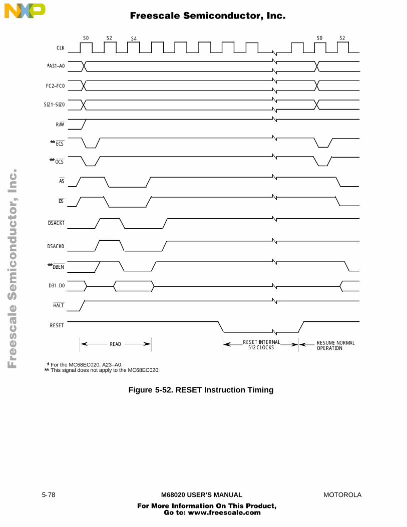
5-78 M68020 USER’S MANUAL MOTOROLA
CLK
A31–A0
FC2–FC0
R/W
ECS
OCS
AS
DS
DSACK0
DBEN
SIZ1–SIZ0
DSACK1
HALT
S0 S2S4
D31–D0
S2S0
RESET
READ RESET INTERNAL512 CLOCKS
RESUME NORMALOPERATION
**
**
**
*
* For the MC68EC020, A23–A0.This signal does not apply to the MC68EC020.**
Figure 5-52. RESET Instruction Timing
Fre
esc
ale
Se
mic
on
du
cto
r, I
Freescale Semiconductor, Inc.
For More Information On This Product, Go to: www.freescale.com
nc
...

MOTOROLA M68020 USER’S MANUAL 6-1
SECTION 6EXCEPTION PROCESSING
Exception processing is defined as the activities performed by the processor in preparingto execute a handler routine for any condition that causes an exception. In particular,exception processing does not include execution of the handler routine itself. Anintroduction to exception processing, as one of the processing states of theMC68020/EC020, is given in Section 2 Processing States .
This section describes exception processing in detail, describing the processing for eachtype of exception. It describes the return from an exception and bus fault recovery. Thissection also describes the formats of the exception stack frames. For more detail onprotocol violation and coprocessor-related exceptions, refer to Section 7 CoprocessorInterface Description . Also, for more detail on exceptions defined for floating-pointcoprocessors, refer to MC68881UM/AD, MC68881/MC68882 Floating-Point CoprocessorUser's Manual.
6.1 EXCEPTION PROCESSING SEQUENCE
Exception processing occurs in four functional steps. However, all individual bus cyclesassociated with exception processing (vector acquisition, stacking, etc.) are notguaranteed to occur in the order in which they are described in this section. Nonetheless,all addresses and offsets from the stack pointer are guaranteed to be as described.
The first step of exception processing involves the SR. The processor makes an internalcopy of the SR, then sets the S-bit in the SR, changing to the supervisor privilege level.Next, the processor inhibits tracing of the exception handler by clearing the T1 and T0 bitsin the SR. For the reset and interrupt exceptions, the processor also updates the interruptpriority mask (bits 10–8 of the SR).
In the second step, the processor determines the vector number of the exception. Forinterrupts, the processor performs an interrupt acknowledge cycle (a read from the CPUaddress space type 1111; see Figures 5-32 and 5-33) to obtain the vector number. Forcoprocessor-detected exceptions, the vector number is included in the coprocessorexception primitive response. (Refer to Section 7 Coprocessor Interface Description fora complete discussion of coprocessor exceptions.) For all other exceptions, internal logicprovides the vector number. This vector number is used in the last step to calculate theaddress of the exception vector. Throughout this section, vector numbers are given indecimal notation.
Fre
esc
ale
Se
mic
on
du
cto
r, I
Freescale Semiconductor, Inc.
For More Information On This Product, Go to: www.freescale.com
nc
...
6-2 M68020 USER’S MANUAL MOTOROLA
For all exceptions other than reset, the third step is to save the current processor context.The processor creates an exception stack frame on the active supervisor stack and fills itwith context information appropriate for the type of exception. Other information may alsobe stacked, depending on which exception is being processed and the state of theprocessor prior to the exception. If the exception is an interrupt and the M-bit in the SR isset, the processor clears the M-bit and builds a second stack frame on the interrupt stack.
The last step initiates execution of the exception handler. The processor multiplies thevector number by four to determine the exception vector offset. The processor then addsthe offset to the value stored in the VBR to obtain the memory address of the exceptionvector. Next, the processor loads the PC (and the ISP for the reset exception) from theexception vector table in memory. After prefetching the first three words to fill theinstruction pipe, the processor resumes normal processing at the address in the PC. Table6-1 contains a description of all the exception vector offsets defined for theMC68020/EC020.
As shown in Table 6-1, the first 64 vectors are defined by Motorola, and 192 vectors arereserved for interrupt vectors defined by the user. However, external devices may usevectors reserved for internal purposes at the discretion of the system designer.
Fre
esc
ale
Se
mic
on
du
cto
r, I
Freescale Semiconductor, Inc.
For More Information On This Product, Go to: www.freescale.com
nc
...

MOTOROLA M68020 USER’S MANUAL 6-3
Table 6-1. Exception Vector Assignments
Vector Offset
Vector Number Hex Space Assignment
0123
00000400800C
SPSPSDSD
Reset Initial Interrupt Stack PointerReset Initial Program CounterBus ErrorAddress Error
4567
01001401801C
SDSDSDSD
Illegal InstructionZero DivideCHK, CHK2 InstructioncpTRAPcc, TRAPcc, TRAPV Instructions
89
1011
02002402802C
SDSDSDSD
Privilege ViolationTraceLine 1010 EmulatorLine 1111 Emulator
12131415
03003403803C
SDSDSDSD
(Unassigned, Reserved)Coprocessor Protocol ViolationFormat ErrorUninitialized Interrupt
16–23 04005C
SDSD
Unassigned, Reserved
24252627
06006406806C
SDSDSDSD
Spurious InterruptLevel 1 Interrupt AutovectorLevel 2 Interrupt AutovectorLevel 3 Interrupt Autovector
28293031
07007407807C
SDSDSDSD
Level 4 Interrupt AutovectorLevel 5 Interrupt AutovectorLevel 6 Interrupt AutovectorLevel 7 Interrupt Autovector
32–47 0800BC
SDSD
TRAP #0–15 Instruction Vectors
48495051
0C00C40C80CC
SDSDSDSD
FPCP Branch or Set on Unordered ConditionFPCP Inexact ResultFPCP Divide by ZeroFPCP Underflow
52535455
0D00D40D80DC
SDSDSDSD
FPCP Operand ErrorFPCP OverflowFPCP Signaling NANUnassigned, Reserved
565758
0E00E40E8
SDSDSD
PMMU ConfigurationPMMU Illegal OperationPMMU Access Level Violation
59–63 0EC0FC
SDSD
Unassigned, Reserved
64–255 1003FC
SDSD
User-Defined Vectors (192)
SP—Supervisor Program SpaceSD—Supervisor Data Space
Fre
esc
ale
Se
mic
on
du
cto
r, I
Freescale Semiconductor, Inc.
For More Information On This Product, Go to: www.freescale.com
nc
...

6-4 M68020 USER’S MANUAL MOTOROLA
6.1.1 Reset Exception
Assertion of the RESET signal by external hardware causes a reset exception. For detailson the requirements for the assertion of RESET, refer to Section 5 Bus Operation.
The reset exception has the highest priority of any exception; it provides for systeminitialization and recovery from catastrophic failure. When a reset exception is recognized,it aborts any processing in progress and that processing cannot be recovered. Figure 6-1is a flowchart of the reset exception, which performs the following operations:
1. Clears the T1 and T0 bits in the SR to disable tracing.
2. Places the processor in the interrupt mode of the supervisor privilege level by settingthe S-bit and clearing the M-bit in the SR.
3. Sets the I2–I0 bits in the SR to the highest priority level (level 7).
4. Initializes the VBR to zero ($00000000).
5. Clears the E and F bits in the CACR.
6. Invalidates all entries in the instruction cache.
7. Generates a vector number to reference the reset exception vector (two long words)at offset zero in the supervisor program address space.
8. Loads the first long word of the reset exception vector into the interrupt stack pointer.
9. Loads the second long word of the reset exception vector into the PC.
After the initial instruction prefetches, program execution begins at the address in the PC.The reset exception does not save the value of either the PC or the SR.
As described in Section 5 Bus Operation, if a bus error or address error occurs duringthe exception processing sequence for a reset, a double bus fault occurs. The processorhalts and asserts the HALT signal to indicate the halted condition.
Execution of the RESET instruction does not cause a reset exception, nor does it affectany internal registers, but it does cause the MC68020/EC020 to assert the RESET signal,resetting all external devices.
6.1.2 Bus Error Exception
A bus error exception occurs when external logic aborts a bus cycle by asserting theBERR signal. If the aborted bus cycle is a data access, the processor immediately beginsexception processing. If the aborted bus cycle is an instruction prefetch, the processormay delay taking the exception until it attempts to use the prefetched information.
Fre
esc
ale
Se
mic
on
du
cto
r, I
Freescale Semiconductor, Inc.
For More Information On This Product, Go to: www.freescale.com
nc
...
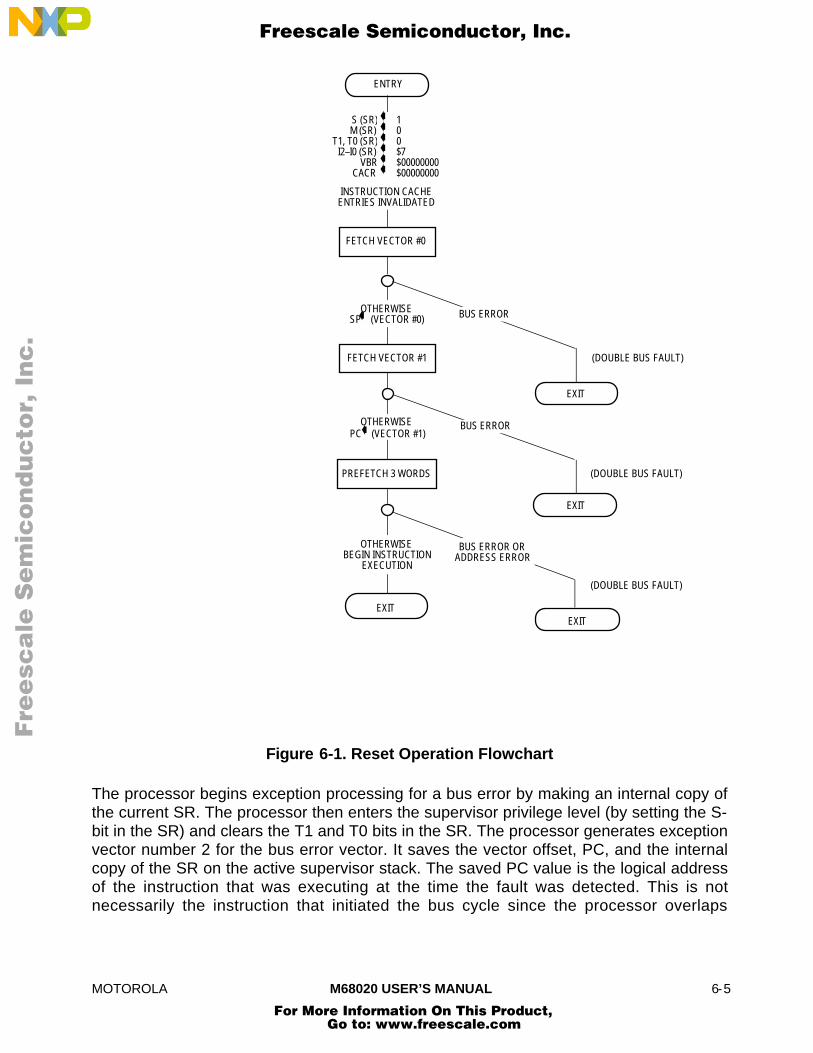
MOTOROLA M68020 USER’S MANUAL 6-5
OTHERWISESP (VECTOR #0)
EXIT
FETCH VECTOR #0
(DOUBLE BUS FAULT)
S (SR)M (SR)
T1, T0 (SR)I2–I0 (SR)
VBRCACR
100$7$00000000$00000000
➧➧➧➧➧➧
(DOUBLE BUS FAULT)
(DOUBLE BUS FAULT)
ENTRY
OTHERWISEBEGIN INSTRUCTION
EXECUTION
OTHERWISE
INSTRUCTION CACHEENTRIES INVALIDATED
➧
FETCH VECTOR #1
PC (VECTOR #1)
➧
PREFETCH 3 WORDS
EXIT
EXIT
EXIT
BUS ERROR
BUS ERROR
BUS ERROR ORADDRESS ERROR
Figure 6-1. Reset Operation Flowchart
The processor begins exception processing for a bus error by making an internal copy ofthe current SR. The processor then enters the supervisor privilege level (by setting the S-bit in the SR) and clears the T1 and T0 bits in the SR. The processor generates exceptionvector number 2 for the bus error vector. It saves the vector offset, PC, and the internalcopy of the SR on the active supervisor stack. The saved PC value is the logical addressof the instruction that was executing at the time the fault was detected. This is notnecessarily the instruction that initiated the bus cycle since the processor overlaps
Fre
esc
ale
Se
mic
on
du
cto
r, I
Freescale Semiconductor, Inc.
For More Information On This Product, Go to: www.freescale.com
nc
...
6-6 M68020 USER’S MANUAL MOTOROLA
execution of instructions. The processor also saves the contents of some of its internalregisters. The information saved on the stack is sufficient to identify the cause of the busfault and recover from the error.
For efficiency, the MC68020/EC020 uses two different bus error stack frame formats.When the bus error exception is taken at an instruction boundary, less information isrequired to recover from the error, and the processor builds the short bus fault stack frameas shown in Table 6-5. When the exception is taken during the execution of an instruction,the processor must save its entire state for recovery and uses the long bus fault stackframe shown in Table 6-5. The format code in the stack frame distinguishes the two stackframe formats. Stack frame formats are described in detail in 6.4 Exception Stack FrameFormats.
If a bus error occurs during the exception processing for a bus error, address error, orreset or while the processor is loading internal state information from the stack during theexecution of an RTE instruction, a double bus fault occurs and the processor enters thehalted state. In this case, the processor does not attempt to alter the current state ofmemory. Only an external RESET can restart a processor halted by a double bus fault.
6.1.3 Address Error Exception
An address error exception occurs when the processor attempts to prefetch an instructionfrom an odd address. This exception is similar to a bus error exception but is internallyinitiated. A bus cycle is not executed, and the processor begins exception processingimmediately. After exception processing commences, the sequence is the same as thatfor bus error exceptions described in the preceding paragraphs, except that the vectornumber is 3 and the vector offset in the stack frame refers to the address error vector.Either a short or long bus fault stack frame may be generated. If an address error occursduring the exception processing for a bus error, address error, or reset, a double bus faultoccurs.
6.1.4 Instruction Trap Exception
Certain instructions are used to explicitly cause trap exceptions. The TRAP instructionalways forces an exception and is useful for implementing system calls in user programs.The TRAPcc, TRAPV, cpTRAPcc, CHK, and CHK2 instructions force exceptions if theuser program detects an error, which may be an arithmetic overflow or a subscript valuethat is out of bounds.
The DIVS and DIVU instructions force exceptions if a division operation is attempted witha divisor of zero.
When a trap exception occurs, the processor copies the SR internally, enters thesupervisor privilege level (by setting the S-bit in the SR), and clears the T1 and T0 bits inthe SR. If tracing is enabled for the instruction that caused the trap, a trace exception istaken after the RTE instruction from the trap handler is executed, and the tracecorresponds to the trap instruction; the trap handler routine is not traced. The processorgenerates a vector number according to the instruction being executed; for the TRAP
Fre
esc
ale
Se
mic
on
du
cto
r, I
Freescale Semiconductor, Inc.
For More Information On This Product, Go to: www.freescale.com
nc
...
MOTOROLA M68020 USER’S MANUAL 6-7
instruction, the vector number is 32 plus n. The stack frame saves the trap vector offset,the PC, and the internal copy of the SR on the supervisor stack. The saved value of thePC is the logical address of the instruction following the instruction that caused the trap.For all instruction traps other than TRAP, a pointer to the instruction that caused the trapis also saved. Instruction execution resumes at the address in the exception vector afterthe required instruction prefetches.
6.1.5 Illegal Instruction and Unimplemented Instruction Exceptions
An illegal instruction is an instruction that contains any bit pattern in its first word that doesnot correspond to the bit pattern of the first word of a valid MC68020/EC020 instruction ora MOVEC instruction with an undefined register specification field in the first extensionword. An illegal instruction exception corresponds to vector number 4 and occurs whenthe processor attempts to execute an illegal instruction.
An illegal instruction exception is also taken if a breakpoint acknowledge bus cycle (seeSection 5 Bus Operation) is terminated with the assertion of the BERR signal. Thisimplies that the external circuitry did not supply an instruction word to replace the BKPTinstruction word in the instruction pipe.
Instruction word patterns with bits 15–12 = 1010 are referred to as unimplementedinstructions with A-line opcodes. When the processor attempts to execute anunimplemented instruction with an A-line opcode, an exception is generated with vectornumber 10, permitting efficient emulation of unimplemented instructions.
Instructions that have word patterns with bits 15–12 = 1111, bits 11–9 = 000, and definedword patterns for subsequent words, are legal PMMU instructions. Instructions that havebits 15–12 of the first words = 1111, bits 11–9 = 000, and undefined patterns in thesubsequent words, are treated as unimplemented instructions with F-line opcodes whenexecution is attempted in the supervisor privilege level. When execution of the sameinstruction is attempted in the user privilege level, a privilege violation exception is taken.The exception vector number for an unimplemented instruction with an F-line opcode is11.
The word patterns with bits 15–12 = 1111 and bits 11–9 ≠ 000 are used for coprocessorinstructions. When the processor identifies a coprocessor instruction, it runs a bus cyclereferencing CPU space type $2 (refer to Section 2 Processing States) and addressingone of eight coprocessors (0–7, according to bits 11–9). If the addressed coprocessor isnot included in the system and the cycle terminates with the assertion of BERR, theinstruction takes an unimplemented instruction (F-line opcode) exception. The system canemulate the functions of the coprocessor with an F-line exception handler. Refer toSection 7 Coprocessor Interface Description for more details.
Fre
esc
ale
Se
mic
on
du
cto
r, I
Freescale Semiconductor, Inc.
For More Information On This Product, Go to: www.freescale.com
nc
...
6-8 M68020 USER’S MANUAL MOTOROLA
Exception processing for illegal and unimplemented instructions is similar to that forinstruction traps. When the processor has identified an illegal or unimplementedinstruction, it initiates exception processing instead of attempting to execute theinstruction. The processor copies the SR, enters the supervisor privilege level (by settingthe S bit in the SR), and clears the T1 and T0 bits in the SR, disabling further tracing. Theprocessor generates the vector number, either 4, 10, or 11, according to the exceptiontype. The illegal or unimplemented instruction vector offset, current PC, and copy of theSR are saved on the supervisor stack, with the saved value of the PC being the addressof the illegal or unimplemented instruction. Instruction execution resumes at the addresscontained in the exception vector. It is the responsibility of the handling routine to adjustthe stacked PC if the instruction is emulated in software or is to be skipped on return fromthe handler.
6.1.6 Privilege Violation Exception
To provide system security, the following instructions are privileged:
ANDI to SREORI to SRcpRESTOREcpSAVEMOVE from SRMOVE to SRMOVE USPMOVECMOVESORI to SRRESETRTESTOP
An attempt to execute one of the privileged instructions while at the user privilege levelcauses a privilege violation exception. Also, a privilege violation exception occurs if acoprocessor requests a privilege check and the processor is at the user level.
Exception processing for privilege violations is similar to that for illegal instructions. Whenthe processor identifies a privilege violation, it begins exception processing beforeexecuting the instruction. The processor copies the SR, enters the supervisor privilegelevel by setting the S-bit in the SR, and clears the T1 and T0 bits in the SR. The processorgenerates vector number 8, the privilege violation exception vector, and saves theprivilege violation vector offset, the current PC value, and the internal copy of the SR onthe supervisor stack. The saved value of the PC is the logical address of the first word ofthe instruction that caused the privilege violation. Instruction execution resumes after therequired prefetches from the address in the privilege violation exception vector.
Fre
esc
ale
Se
mic
on
du
cto
r, I
Freescale Semiconductor, Inc.
For More Information On This Product, Go to: www.freescale.com
nc
...

MOTOROLA M68020 USER’S MANUAL 6-9
6.1.7 Trace Exception
To aid in program development, the M68000 processors include an instruction-by-instruction tracing capability. The MC68020/EC020 can be programmed to trace allinstructions or only instructions that change program flow. In the trace mode, aninstruction generates a trace exception after it completes execution, allowing a debuggerprogram to monitor execution of a program.
The T1 and T0 bits in the supervisor portion of the SR control tracing. The state of thesebits when an instruction begins execution determines whether the instruction generates atrace exception after the instruction completes. Clearing both the T1 and T0 bits disablestracing, and instruction execution proceeds normally. Clearing the T1 bit and setting theT0 bit causes an instruction that forces a change of flow to take a trace exception.Instructions that increment the PC normally do not take the trace exception. Instructionsthat are traced in this mode include all branches, jumps, instruction traps, returns, andcoprocessor instructions that modify the PC flow. This mode also includes SRmanipulations because the processor must re-prefetch instruction words to fill the pipeagain any time an instruction that can modify the SR is executed. The execution of theBKPT instruction causes a change of flow if the opcode replacing the BKPT is aninstruction that causes a change of flow (i.e., a jump, branch, etc.). Setting the T1 bit andclearing the T0 bit causes the execution of all instructions to force trace exceptions. Table6-2 shows the trace mode selected by each combination of T1 and T0.
Table 6-2. Tracing Control
TI T0 Tracing Function
0 0 No Tracing
0 1 Trace on Change of Flow (BRA, JMP, etc.)
1 0 Trace on Instruction Execution (Any Instruction)
1 1 Undefined, Reserved
In general terms, a trace exception is an extension to the function of any tracedinstruction—i.e., the execution of a traced instruction is not complete until completion oftrace exception processing. If an instruction does not complete due to a bus error oraddress error exception, trace exception processing is deferred until after the execution ofthe suspended instruction is resumed, and the instruction execution completes normally. Ifan interrupt is pending at the completion of an instruction, the trace exception processingoccurs before the interrupt exception processing starts. If an instruction forces anexception as part of its normal execution, the forced exception processing occurs beforethe trace exception is processed. See 6.1.11 Multiple Exceptions for a more completediscussion of exception priorities.
When tracing is enabled and the processor attempts to execute an illegal orunimplemented instruction, that instruction does not cause a trace exception since it is notexecuted. This is of particular importance to an instruction emulation routine that performsthe instruction function, adjusts the stacked PC to skip the unimplemented instruction, andreturns. Before returning, the T1 and T0 bits of the SR on the stack should be checked. If
Fre
esc
ale
Se
mic
on
du
cto
r, I
Freescale Semiconductor, Inc.
For More Information On This Product, Go to: www.freescale.com
nc
...

6-10 M68020 USER’S MANUAL MOTOROLA
tracing is enabled, the trace exception processing should also be emulated for the traceexception handler to account for the emulated instruction.
The exception processing for a trace starts at the end of normal processing for the tracedinstruction and before the start of the next instruction. The processor makes an internalcopy of the SR and enters the supervisor privilege level (by setting the S-bit in the SR). Italso clears the T0 and T1 bits of the SR, disabling further tracing. The processor suppliesvector number 9 for the trace exception and saves the trace exception vector offset, PCvalue, and the copy of the SR on the supervisor stack. The saved value of the PC is thelogical address of the next instruction to be executed. Instruction execution resumes afterthe required prefetches from the address in the trace exception vector.
The STOP instruction does not perform its function when it is traced. A STOP instructionthat begins execution with T1, T0 = 10 forces a trace exception after it loads the SR. Uponreturn from the trace handler routine, execution continues with the instruction following theSTOP instruction, and the processor never enters the stopped condition.
6.1.8 Format Error Exception
Just as the processor checks that prefetched instructions are valid, the processor (with theaid of a coprocessor, if needed) also performs some checks of data values for controloperations, including the type and option fields of the descriptor for CALLM, thecoprocessor state frame format word for a cpRESTORE instruction, and the stack frameformat for an RTE or an RTM instruction.
The RTE instruction checks the validity of the stack format code. For long bus fault formatframes, the RTE instruction also compares the internal version number of the processor tothat contained in the frame at memory location SP + 54 (SP + $36). This check ensuresthat the processor can correctly interpret internal state information from the stack frame.
The CALLM and RTM both check the values in the option and type fields in the moduledescriptor and module stack frame, respectively. If these fields do not contain propervalues or if an illegal access rights change request is detected by an external memorymanagement unit, then an illegal call or return is being requested and is not executed.Refer to Section 9 Applications Information for more information on the modulecall/return mechanism.
The cpRESTORE instruction passes the format word of the coprocessor state frame to thecoprocessor for validation. If the coprocessor does not recognize the format value, itsignals the MC68020/EC020 to take a format error exception. Refer to Section 7Coprocessor Interface Description for details of coprocessor-related exceptions.
If any of the checks previously described determine that the format of the stacked data isimproper, the instruction generates a format error exception. This exception saves a shortbus fault stack frame, generates exception vector number 14, and continues execution atthe address in the format exception vector. The stacked PC value is the logical address ofthe instruction that detected the format error.
Fre
esc
ale
Se
mic
on
du
cto
r, I
Freescale Semiconductor, Inc.
For More Information On This Product, Go to: www.freescale.com
nc
...

MOTOROLA M68020 USER’S MANUAL 6-11
6.1.9 Interrupt Exceptions
When a peripheral device requires the services of the MC68020/EC020 or is ready tosend information that the processor requires, it may signal the processor to take aninterrupt exception. The interrupt exception transfers control to a routine that respondsappropriately.
The peripheral device uses the IPL2–IPL0 signals to signal an interrupt condition to theprocessor and to specify the priority of that condition. These three signals encode a valueof zero through seven (IPL0 is the least significant bit). When IPL2–IPL0 are all negated,the interrupt request level is zero. IPL2–IPL0 values 1–7 specify one of seven levels ofprioritized interrupts; level 7 has the highest priority. External circuitry can chain orotherwise merge signals from devices at each level, allowing an unlimited number ofdevices to interrupt the processor.
The IPL2–IPL0 signals must maintain the interrupt request level until theMC68020/EC020 acknowledges the interrupt to guarantee that the interrupt is recognized.The MC68020/EC020 continuously samples the IPL2–IPL0 signals on consecutive fallingedges of the processor clock to synchronize and debounce these signals. An interruptrequest that is the same for two consecutive falling clock edges is considered a validinput. Although the protocol requires that the request remain until the processor runs aninterrupt acknowledge cycle for that interrupt value, an interrupt request that is held for asshort a period as two clock cycles could be recognized.
The I2–I0 bits in the SR specify the interrupt priority mask. The value in the interrupt maskis the highest priority level that the processor ignores. When an interrupt request has apriority higher than the value in the mask, the processor makes the request a pendinginterrupt. Figure 6-2 is a flowchart of the procedure for making an interrupt pending.
When several devices are connected to the same interrupt level, each device should holdits interrupt priority level constant until its corresponding interrupt acknowledge cycle toensure that all requests are processed.
Table 6-3 lists the interrupt levels, the states of IPL2–IPL0 that define each level, and themask value that allows an interrupt at each level.
Fre
esc
ale
Se
mic
on
du
cto
r, I
Freescale Semiconductor, Inc.
For More Information On This Product, Go to: www.freescale.com
nc
...

6-12 M68020 USER’S MANUAL MOTOROLA
RESET
SAMPLE AND SYNCHIPL2–IPL0
INTERRUPT PENDING(MC68020 ASSERTS IPEND )
(COMPARE INTERRUPT LEVELWITH STATUS REGISTER MASK)
INTERRUPT LEVEL I2–I0,OR TRANSITION ON LEVEL 7
>
*
* IPEND is not implemented in the MC68EC020.
OTHERWISE
Figure 6-2. Interrupt Pending Procedure
Table 6-3. Interrupt Levels and Mask Values
Control Line Status
RequestedInterrupt Level IPL2 IPL1 IPL0
Interrupt Mask ValueRequired for Recognition
0* N N N N/A*
1 N N A 0
2 N A N 1–0
3 N A A 2–0
4 A N N 3–0
5 A N A 4–0
6 A A N 5–0
7 A A A 7–0
*Indicates that no interrupt is requested.A—AssertedN—Negated
Priority level 7, the nonmaskable interrupt, is a special case. Level 7 interrupts cannot bemasked by the interrupt priority mask, and they are transition sensitive. The processorrecognizes an interrupt request each time the external interrupt request level changesfrom some lower level to level 7, regardless of the value in the mask. Figure 6-3 showstwo examples of interrupt recognitions, one for level 6 and one for level 7. When theMC68020/EC020 processes a level 6 interrupt, the interrupt priority mask is automaticallyupdated with a value of 6 before entering the handler routine so that subsequent level 6interrupts are masked. Provided no instruction that lowers the mask value is executed, the
Fre
esc
ale
Se
mic
on
du
cto
r, I
Freescale Semiconductor, Inc.
For More Information On This Product, Go to: www.freescale.com
nc
...

MOTOROLA M68020 USER’S MANUAL 6-13
external request can be lowered to level 3 and then raised back to level 6, and a second
Fre
esc
ale
Se
mic
on
du
cto
r, I
Freescale Semiconductor, Inc.
For More Information On This Product, Go to: www.freescale.com
nc
...
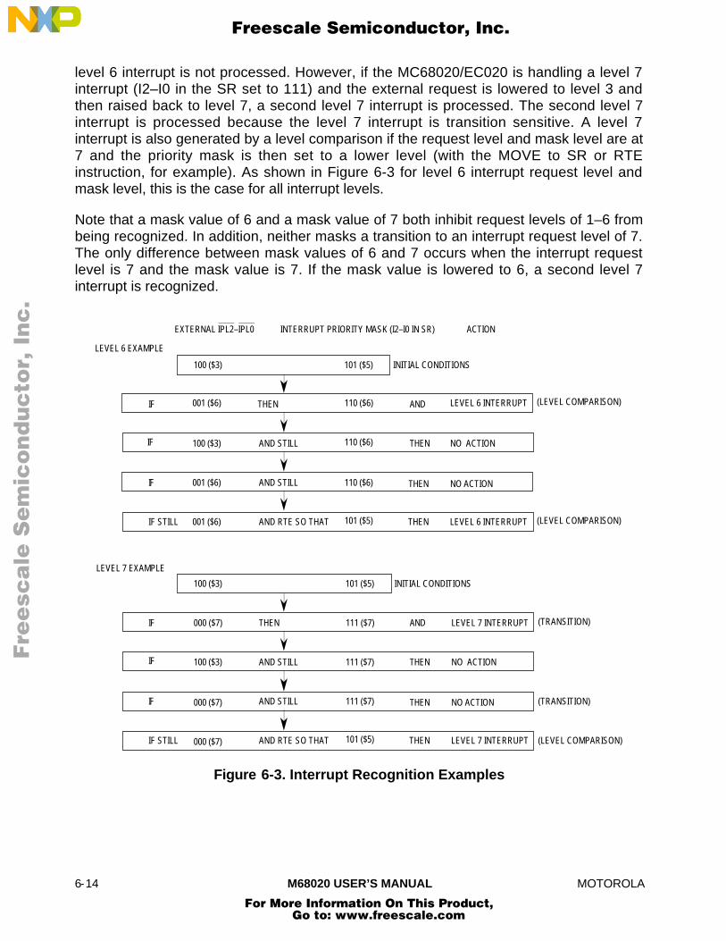
6-14 M68020 USER’S MANUAL MOTOROLA
level 6 interrupt is not processed. However, if the MC68020/EC020 is handling a level 7interrupt (I2–I0 in the SR set to 111) and the external request is lowered to level 3 andthen raised back to level 7, a second level 7 interrupt is processed. The second level 7interrupt is processed because the level 7 interrupt is transition sensitive. A level 7interrupt is also generated by a level comparison if the request level and mask level are at7 and the priority mask is then set to a lower level (with the MOVE to SR or RTEinstruction, for example). As shown in Figure 6-3 for level 6 interrupt request level andmask level, this is the case for all interrupt levels.
Note that a mask value of 6 and a mask value of 7 both inhibit request levels of 1–6 frombeing recognized. In addition, neither masks a transition to an interrupt request level of 7.The only difference between mask values of 6 and 7 occurs when the interrupt requestlevel is 7 and the mask value is 7. If the mask value is lowered to 6, a second level 7interrupt is recognized.
EXTERNAL IPL2–IPL0 INTERRUPT PRIORITY MASK (I2–I0 IN SR) ACTION
LEVEL 6 EXAMPLE
INITIAL CONDITIONS100 ($3) 101 ($5)
(LEVEL COMPARISON)IF 001 ($6) THEN 110 ($6) AND LEVEL 6 INTERRUPT
IF 100 ($3) AND STILL 110 ($6) THEN NO ACTION
IF 001 ($6) AND STILL 110 ($6) THEN NO ACTION
IF STILL 001 ($6) AND RTE SO THAT 101 ($5) THEN LEVEL 6 INTERRUPT (LEVEL COMPARISON)
(TRANSITION)
(TRANSITION)
LEVEL 7 EXAMPLE
INITIAL CONDITIONS100 ($3) 101 ($5)
IF 000 ($7) THEN 111 ($7) AND LEVEL 7 INTERRUPT
IF 100 ($3) AND STILL 111 ($7) THEN NO ACTION
IF 000 ($7) AND STILL 111 ($7) THEN NO ACTION
IF STILL 000 ($7) AND RTE SO THAT 101 ($5) THEN LEVEL 7 INTERRUPT (LEVEL COMPARISON)
Figure 6-3. Interrupt Recognition Examples
Fre
esc
ale
Se
mic
on
du
cto
r, I
Freescale Semiconductor, Inc.
For More Information On This Product, Go to: www.freescale.com
nc
...

MOTOROLA M68020 USER’S MANUAL 6-15
The MC68020 asserts IPEND (note that IPEND is not implemented in the MC68EC020)when it makes an interrupt request pending. Figure 6-4 shows the assertion of IPENDrelative to the assertion of an interrupt level on IPL2–IPL0. IPEND signals to externaldevices that an interrupt exception will be taken at an upcoming instruction boundary(following any higher priority exception). The state of the IPEND signal is internallychecked by the processor once per instruction, independently of bus operation. Inaddition, it is checked during the second instruction prefetch associated with exceptionprocessing.
Figure 6-5 is a flowchart of the interrupt recognition and associated exception processingsequence.
CLK
IPL2–IPL0
IPEND
COMPARE REQUEST WITH MASK IN SR
ASSERT IPENDIPL2–IPL0 RECOGNIZED
IPL2–IPL0 SYNCHRONIZED
Figure 6-4. Assertion of IPEND (MC68020 Only)
Fre
esc
ale
Se
mic
on
du
cto
r, I
Freescale Semiconductor, Inc.
For More Information On This Product, Go to: www.freescale.com
nc
...

6-16 M68020 USER’S MANUAL MOTOROLA
TEMPS
T1, T0
SR1 0
➧➧
➧
UPDATE I2–I0
➧➧
➧➧
– (SP) TEMP– (SP) PC
– (SP) FORMAT WORD– (SP) OTHER EXCEPTION DEPENDENT INFORMATION
ONCE PER INSTRUCTION
EXECUTE INTERRUPT ACKNOWLEDGE CYCLE
AT INSTRUCTIONBOUNDARY
EXIT
M = 1
TEMP SRM 0
➧➧
M = 0PC VECTOR TABLE ENTRY
➧
PREFETCH 3 WORDS
END OF EXCEPTION PROCESSINGFOR THE INTERRUPT
BEGIN EXECUTION OF THE INTERRUPT HANDLER ROUTINE OR PROCESS A HIGHER PRIORITY EXCEPTION
THESEINDIVIDUAL
BUS CYCLESMAY OCCUR
IN ANY ORDER
NEGATE IPEND*
OTHERWISE
IPEND ASSERTED*
Does not apply to the MC68EC020.*
Figure 6-5. Interrupt Exception Processing Flowchart
Fre
esc
ale
Se
mic
on
du
cto
r, I
Freescale Semiconductor, Inc.
For More Information On This Product, Go to: www.freescale.com
nc
...

MOTOROLA M68020 USER’S MANUAL 6-17
For the MC68020, if no higher priority interrupt has been synchronized, the IPEND signalis negated during state 0 (S0) of an interrupt acknowledge cycle, and the IPL2–IPL0signals for the interrupt being acknowledged can be negated at this time. For theMC68EC020, if no higher priority interrupt has been synchronized, the IPL2–IPL0 signalsfor the interrupt being acknowledged can be negated at this time. Refer to Section 5 BusOperation for more information on interrupt acknowledge cycles.
When processing an interrupt exception, the MC68020/EC020 first makes an internal copyof the SR, sets the privilege level to supervisor, suppresses tracing, and sets theprocessor interrupt mask level to the level of the interrupt being serviced. The processorattempts to obtain a vector number from the interrupting device using an interruptacknowledge bus cycle with the interrupt level number output on pins A3–A1 of theaddress bus. For a device that cannot supply an interrupt vector, the AVEC signal can beasserted, and the MC68020/EC020 uses an internally generated autovector, which is oneof vector numbers 31–25, that corresponds to the interrupt level number. If external logicindicates a bus error during the interrupt acknowledge cycle, the interrupt is consideredspurious, and the processor generates the spurious interrupt vector number (24). Refer toSection 5 Bus Operation for complete interrupt bus cycle information.
Once the vector number is obtained, the processor saves the exception vector offset, PCvalue, and the internal copy of the SR on the active supervisor stack. The saved value ofthe PC is the logical address of the instruction that would have been executed had theinterrupt not occurred. If the interrupt was acknowledged during the execution of acoprocessor instruction, further internal information is saved on the stack so that theMC68020/EC020 can continue executing the coprocessor instruction when the interrupthandler completes execution.
If the M-bit in the SR is set, the processor clears the M-bit and creates a throwawayexception stack frame on top of the interrupt stack as part of interrupt exceptionprocessing. This second frame contains the same PC value and vector offset as the framecreated on top of the master stack, but has a format number of 1 instead of 0 or 9. Thecopy of the SR saved on the throwaway frame is exactly the same as that placed on themaster stack except that the S-bit is set in the version placed on the interrupt stack. (Itmay or may not be set in the copy saved on the master stack.) The resulting SR (afterexception processing) has the S-bit set and the M-bit cleared.
The processor loads the address in the exception vector into the PC, and normalinstruction execution resumes after the required prefetches for the interrupt handlerroutine.
Most M68000 family peripherals use programmable interrupt vector numbers as part ofthe interrupt request/acknowledge mechanism of the system. If this vector number is notinitialized after reset and the peripheral must acknowledge an interrupt request, theperipheral usually returns the uninitialized interrupt vector number (15).
Fre
esc
ale
Se
mic
on
du
cto
r, I
Freescale Semiconductor, Inc.
For More Information On This Product, Go to: www.freescale.com
nc
...

6-18 M68020 USER’S MANUAL MOTOROLA
6.1.10 Breakpoint Instruction Exception
To use the MC68020/EC020 in a hardware emulator, it must provide a means of insertingbreakpoints in the emulator code and of performing appropriate operations at eachbreakpoint. For the MC68000 and MC68008, this can be done by inserting an illegalinstruction at the breakpoint and detecting the illegal instruction exception from its vectorlocation. However, since the VBR on M68000 family processors MC68010 and laterallows arbitrary relocation of exception vectors, the exception address cannot reliablyidentify a breakpoint. The MC68020/EC020 processor provides a breakpoint capabilitywith a set of breakpoint instructions, $4848–$484F, for eight unique breakpoints. Thebreakpoint facility also allows external hardware to monitor the execution of a programresiding in the on-chip instruction cache without severe performance degradation.
When the MC68020/EC020 executes a breakpoint instruction, it performs a breakpointacknowledge cycle (read cycle) from CPU space type $0 with address lines A4–A2corresponding to the breakpoint number. Refer to Section 5 Bus Operation for adescription of the breakpoint acknowledge cycle. The external hardware can return eitherBERR or DSACK1/DSACK0 with an instruction word on the data bus. If the bus cycleterminates with BERR, the processor performs illegal instruction exception processing. Ifthe bus cycle terminates with DSACK1/DSACK0, the processor uses the data returned toreplace the breakpoint instruction in the internal instruction pipe and begins execution ofthat instruction. The remainder of the pipe remains unaltered. In addition, no stacking orvector fetching is involved with the execution of the instruction. Figure 6-6 is a flowchart ofthe breakpoint instruction execution.
6.1.11 Multiple Exceptions
When several exceptions occur simultaneously, they are processed according to a fixedpriority. Table 6-4 lists the exceptions grouped by characteristics. Each group has apriority from 4–0. Priority 0 has the highest priority.
As soon as the MC68020/EC020 has completed exception processing for a conditionwhen another exception is pending, it begins exception processing for the pendingexception instead of executing the exception handler for the original exception condition.Also, whenever a bus error or address error occurs, its exception processing takesprecedence over lower priority exceptions and occurs immediately. For example, if a buserror occurs during the exception processing for a trace condition, the system processesthe bus error and executes its handler before completing the trace exception processing.However, most exceptions cannot occur during exception processing, and very fewcombinations of the exceptions shown in Table 6-4 can be pending simultaneously.
Fre
esc
ale
Se
mic
on
du
cto
r, I
Freescale Semiconductor, Inc.
For More Information On This Product, Go to: www.freescale.com
nc
...
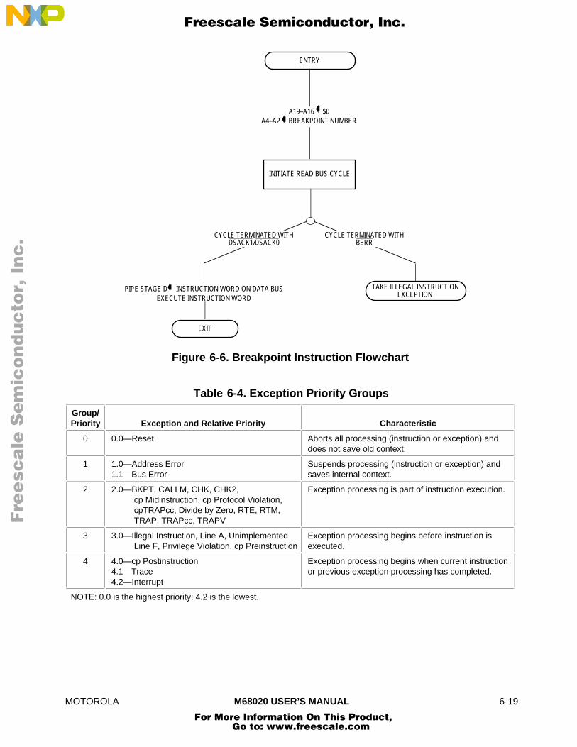
MOTOROLA M68020 USER’S MANUAL 6-19
EXIT
ENTRY
INITIATE READ BUS CYCLE
CYCLE TERMINATED WITHBERR
PIPE STAGE D INSTRUCTION WORD ON DATA BUSEXECUTE INSTRUCTION WORD
➧
TAKE ILLEGAL INSTRUCTIONEXCEPTION
A19–A16 $0A4–A2 BREAKPOINT NUMBER
➧
➧
CYCLE TERMINATED WITHDSACK1/DSACK0
Figure 6-6. Breakpoint Instruction Flowchart
Table 6-4. Exception Priority Groups
Group/Priority Exception and Relative Priority Characteristic
0 0.0—Reset Aborts all processing (instruction or exception) anddoes not save old context.
1 1.0—Address Error1.1—Bus Error
Suspends processing (instruction or exception) andsaves internal context.
2 2.0—BKPT, CALLM, CHK, CHK2,cp Midinstruction, cp Protocol Violation,cpTRAPcc, Divide by Zero, RTE, RTM,TRAP, TRAPcc, TRAPV
Exception processing is part of instruction execution.
3 3.0—Illegal Instruction, Line A, UnimplementedLine F, Privilege Violation, cp Preinstruction
Exception processing begins before instruction isexecuted.
4 4.0—cp Postinstruction4.1—Trace4.2—Interrupt
Exception processing begins when current instructionor previous exception processing has completed.
NOTE: 0.0 is the highest priority; 4.2 is the lowest.
Fre
esc
ale
Se
mic
on
du
cto
r, I
Freescale Semiconductor, Inc.
For More Information On This Product, Go to: www.freescale.com
nc
...

6-20 M68020 USER’S MANUAL MOTOROLA
The priority scheme is very important in determining the order in which exception handlersexecute when several exceptions occur at the same time. As a general rule, the lower thepriority of an exception, the sooner the handler routine for that exception executes. Forexample, if simultaneous trap, trace, and interrupt exceptions are pending, the exceptionprocessing for the trap occurs first, followed immediately by exception processing for thetrace, and then for the interrupt. When the processor resumes normal instructionexecution, it is in the interrupt handler, which returns to the trace handler, which returns tothe trap exception handler. This rule does not apply to the reset exception; its handler isexecuted first even though it has the highest priority because the reset operation clears allother exceptions.
6.1.12 Return from Exception
After the MC68020/EC020 has completed exception processing for all pendingexceptions, it resumes normal instruction execution at the address in the vector for the lastexception processed. Once the exception handler has completed execution, the processormust return to the system context prior to the exception (if possible). The RTE instructionreturns from the handler to the previous system context for any exception.
When the processor executes an RTE instruction, it examines the stack frame on top ofthe active supervisor stack to determine if it is a valid frame and what type of contextrestoration it requires. The following paragraphs describe the processing for each of thestack frame types; refer to 6.3 Coprocessor Considerations for a description of thestack frame type formats.
For a normal four-word frame, the processor updates the SR and PC with the data readfrom the stack, increments the stack pointer by eight, and resumes normal instructionexecution.
For the throwaway four-word frame, the processor reads the SR value from the frame,increments the active stack pointer by eight, updates the SR with the value read from thestack, and then begins RTE processing again, as shown in Figure 6-7. The processorreads a new format word from the stack frame on top of the active stack (which may ormay not be the same stack used for the previous operation) and performs the properoperations corresponding to that format. In most cases, the throwaway frame is on theinterrupt stack and when the SR value is read from the stack, the S and M bits are set. Inthat case, there is a normal four-word frame or a ten-word coprocessor midinstructionframe on the master stack. However, the second frame may be any format (even anotherthrowaway frame) and may reside on any of the three system stacks.
For the six-word stack frame, the processor restores the SR and PC values from thestack, increments the active supervisor stack pointer by 12, and resumes normalinstruction execution.
Fre
esc
ale
Se
mic
on
du
cto
r, I
Freescale Semiconductor, Inc.
For More Information On This Product, Go to: www.freescale.com
nc
...

MOTOROLA M68020 USER’S MANUAL 6-21
ENTRY
SR TEMPSP SP + 6
➧
➧
TEMP (SP) +READ FORMAT WORD
➧
OTHERWISE
FORMAT CODE = $1
(THROWAWAY FRAME)
OTHERWISE
PC (SP) +SP SP + 6SR TEMP
➧➧➧
EXIT
OTHER FORMATS
TAKE FORMATERROR EXCEPTION
OTHERWISE
FORMAT CODE = $0 (FOUR-WORD FRAME)
INVALID FORMAT WORD
Figure 6-7. RTE Instruction for Throwaway Four-Word Frame
For the coprocessor midinstruction stack frame, the processor reads the SR, PC,instruction address, internal register values, and the evaluated effective address from thestack, restores these values to the corresponding internal registers, and increments thestack pointer by 20. The processor then reads from the response register of thecoprocessor that initiated the exception to determine the next operation to be performed.Refer to Section 7 Coprocessor Interface Description for details of coprocessor-relatedexceptions.
For both the short and long bus fault stack frames, the processor first checks the formatvalue on the stack for validity. In addition, for the long stack frame, the processorcompares the version number in the stack with its own version number. The versionnumber is located in the most significant nibble (bits 15–12) of the word at location SP +$36 in the long stack frame. This validity check is required in a multiprocessor system toensure that the data is properly interpreted by the RTE instruction. The RTE instructionalso reads from both ends of the stack frame to make sure it is accessible. If the frame isinvalid or inaccessible, the processor takes a format error or a bus error exception,respectively. Otherwise, the processor reads the entire frame into the proper internalregisters, deallocates the stack, and resumes normal processing. Once the processorbegins to load the frame to restore its internal state, the assertion of the BERR signal
Fre
esc
ale
Se
mic
on
du
cto
r, I
Freescale Semiconductor, Inc.
For More Information On This Product, Go to: www.freescale.com
nc
...
6-22 M68020 USER’S MANUAL MOTOROLA
causes the processor to enter the halted state. Refer to 6.2 Bus Fault Recovery for adescription of the processing that occurs after the frame is read into the internal registers.
If a format error or bus error exception occurs during the frame validation sequence of theRTE instruction, either due to any of the errors previously described or due to an illegalformat code, the processor creates a normal four-word or a bus fault stack frame belowthe frame that it was attempting to use. In this way, the faulty stack frame remains intact.The exception handler can examine or repair the faulty frame. In a multiprocessor system,the faulty frame can be left to be used by another processor of a different type (e.g., anMC68010 or a future M68000 family processor) when appropriate.
6.2 BUS FAULT RECOVERY
An address error exception or a bus error exception indicates a bus fault. The saving ofthe processor state for a bus error or address error is described in 6.1.2 Bus ErrorException, and the restoring of the processor state by an RTE instruction is described in6.1.12 Return from Exception.
Processor accesses of either data items or the instruction stream can result in bus errors.When a bus error exception occurs while accessing a data item, the exception is takenimmediately after the bus cycle terminates. The processor may never access aninstruction that is part of the instruction stream. In this case, the bus error would not beprocessed. For instruction faults, when the short bus fault stack frame applies, theaddress of the pipe stage B word is the value in the PC plus four, and the address of thestage C word is the value in the PC plus two. For the long format, the long word at SP +$24 contains the address of the stage B word; the address of the stage C word is theaddress of the stage B word minus two. Address error faults occur only for instructionstream accesses, and the exceptions are taken before the bus cycles are attempted.
6.2.1 Special Status Word (SSW)
The internal SSW (see Figure 6-8) is one of several registers saved as part of the busfault exception stack frame. Both the short bus fault format and the long bus fault formatinclude this word at offset $A. The bus cycle fault stack frame formats are described indetail in 6.4 Exception Stack Frame Formats.
The SSW information indicates whether the fault was caused by an access to theinstruction stream, data stream, or both. The high-order half of the SSW contains twostatus bits each for the B and C stages of the instruction pipe. If an address errorexception occurs, the fault bits written to the stack frame are not set (they are only set dueto a bus error, as previously described), and the rerun bits alone show the cause of theexception. Depending on the state of the pipeline, either RB and RC are set, or only RC isset. To correct the pipeline contents and continue execution of the suspended instruction,software must place the correct instruction stream data in the stage C and/or stage Bimages requested by the rerun bits and must clear the rerun bits. The least significant halfof the SSW applies to data cycles only. Data and instruction stream faults may be pendingsimultaneously; the fault handler should be able to recognize any combination of the FC,FB, RC, RB, and DF bits.
Fre
esc
ale
Se
mic
on
du
cto
r, I
Freescale Semiconductor, Inc.
For More Information On This Product, Go to: www.freescale.com
nc
...
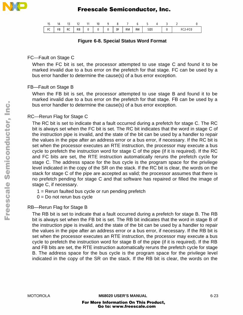
MOTOROLA M68020 USER’S MANUAL 6-23
15 0
FC FB RC
14 13 12
RB
11 10 9 8 7 6 5 4 3 2
0 0 0 DF RM RW SIZE 0 FC2–FC0
Figure 6-8. Special Status Word Format
FC—Fault on Stage CWhen the FC bit is set, the processor attempted to use stage C and found it to bemarked invalid due to a bus error on the prefetch for that stage. FC can be used by abus error handler to determine the cause(s) of a bus error exception.
FB—Fault on Stage BWhen the FB bit is set, the processor attempted to use stage B and found it to bemarked invalid due to a bus error on the prefetch for that stage. FB can be used by abus error handler to determine the cause(s) of a bus error exception.
RC—Rerun Flag for Stage CThe RC bit is set to indicate that a fault occurred during a prefetch for stage C. The RCbit is always set when the FC bit is set. The RC bit indicates that the word in stage C ofthe instruction pipe is invalid, and the state of the bit can be used by a handler to repairthe values in the pipe after an address error or a bus error, if necessary. If the RC bit isset when the processor executes an RTE instruction, the processor may execute a buscycle to prefetch the instruction word for stage C of the pipe (if it is required). If the RCand FC bits are set, the RTE instruction automatically reruns the prefetch cycle forstage C. The address space for the bus cycle is the program space for the privilegelevel indicated in the copy of the SR on the stack. If the RC bit is clear, the words on thestack for stage C of the pipe are accepted as valid; the processor assumes that there isno prefetch pending for stage C and that software has repaired or filled the image ofstage C, if necessary.
1 = Rerun faulted bus cycle or run pending prefetch0 = Do not rerun bus cycle
RB—Rerun Flag for Stage BThe RB bit is set to indicate that a fault occurred during a prefetch for stage B. The RBbit is always set when the FB bit is set. The RB bit indicates that the word in stage B ofthe instruction pipe is invalid, and the state of the bit can be used by a handler to repairthe values in the pipe after an address error or a bus error, if necessary. If the RB bit isset when the processor executes an RTE instruction, the processor may execute a buscycle to prefetch the instruction word for stage B of the pipe (if it is required). If the RBand FB bits are set, the RTE instruction automatically reruns the prefetch cycle for stageB. The address space for the bus cycle is the program space for the privilege levelindicated in the copy of the SR on the stack. If the RB bit is clear, the words on the
Fre
esc
ale
Se
mic
on
du
cto
r, I
Freescale Semiconductor, Inc.
For More Information On This Product, Go to: www.freescale.com
nc
...

6-24 M68020 USER’S MANUAL MOTOROLA
stack for stage B of the pipe are accepted as valid; the processor assumes that there isno prefetch pending for stage B and that software has repaired or filled the image ofstage B, if necessary.
1 = Rerun faulted bus cycle or run pending prefetch0 = Do not rerun bus cycle
Bits 11–9—Reserved by Motorola
DF—Fault/Rerun FlagIf the DF bit is set, a data fault has occurred and caused the exception. If the DF bit isset when the processor reads the stack frame, it reruns the faulted data access;otherwise, it assumes that the data input buffer value on the stack is valid for a read orthat the data has been correctly written to memory for a write (or that no data faultoccurred).
1 = Rerun faulted bus cycle or run pending prefetch0 = Do not rerun bus cycle
RM—Read-Modify-Write1 = Read-modify-write operation on data cycle0 = Not a read-modify-write operation
RW—Read/Write1 = Read on data cycle0 = Write on data cycle
SIZE—Size CodeThe SIZE field indicates the size of the operand access for the data cycle.
Bit 3—Reserved by Motorola
FC2–FC0—Specifies the address space for data cycle
6.2.2 Using Software to Complete the Bus Cycles
One method of completing a faulted bus cycle is to use a software handler to emulate thecycle. This is the only method for correcting address errors. The handler should emulatethe faulted bus cycle in a manner that is transparent to the instruction that caused thefault. For instruction stream faults, the handler may need to run bus cycles for both the Band C stages of the instruction pipe. The RB and RC bits of the SSW identify the stagesthat may require a bus cycle; the FB and FC bits of the SSW indicate that a stage wasinvalid when an attempt was made to use its contents. Those stages must be repaired.For each faulted stage, the software handler should copy the instruction word from theproper address space as indicated by the S-bit of the copy of the SR saved on the stack tothe image of the appropriate stage in the stack frame. In addition, the handler must clearthe RB or RC bit associated with the stage that it has corrected. The handler should notchange the FB and FC bits.
Fre
esc
ale
Se
mic
on
du
cto
r, I
Freescale Semiconductor, Inc.
For More Information On This Product, Go to: www.freescale.com
nc
...

MOTOROLA M68020 USER’S MANUAL 6-25
To repair data faults (indicated by DF = 1), the software should first examine the RM bit inthe SSW to determine if the fault was generated during a read-modify-write operation. IfRM = 0, the handler should then check the RW bit of the SSW to determine if the fault wascaused by a read or a write cycle. For data write faults, the handler must transfer theproperly sized data from the data output buffer on the stack frame to the location indicatedby the data fault address in the address space defined by the SSW. (Both the data outputbuffer and the data fault address are part of the stack frame at SP + $18 and SP + $10,respectively.) Data read faults only generate the long bus fault frame, and the handlermust transfer properly sized data from the location indicated by the fault address andaddress space to the image of the data input buffer at location SP + $2C of the longformat stack frame. Byte, word, and 3-byte operands are right justified in the 4-byte databuffers. In addition, the software handler must clear the DF bit of the SSW to indicate thatthe faulted bus cycle has been corrected.
To emulate a read-modify-write cycle, the exception handler must first read the operationword at the PC address (SP + 2 of the stack frame). This word identifies the CAS, CAS2,or TAS instruction that caused the fault. Then the handler must emulate this entireinstruction (which may consist of up to four long-word transfers) and update the CCRportion of the SR appropriately, because the RTE instruction expects the entire operationto have been completed if the RM bit is set and the DF bit is cleared. This is true even ifthe fault occurred on the first read cycle.
To emulate the entire instruction, the handler must save the data and address registers forthe instruction (with a MOVEM instruction, for example). Next, the handler reads andmodifies (if necessary) the memory location. It clears the DF bit in the SSW of the stackframe and modifies the condition codes in the SR copy and the copies of any data oraddress registers required for the CAS and CAS2 instructions. Last, the handler restoresthe registers that it saved at the beginning of the emulation. Except for the data inputbuffer, the copy of the SR, and the SSW, the handler should not modify a bus fault stackframe. The only bits in the SSW that may be modified are DF, RB, and RC; all other bits,including those defined for internal use, must remain unchanged.
Address error faults must be repaired in software. Address error faults can bedistinguished from bus error faults by the value in the vector offset field of the format word.
6.2.3 Completing the Bus Cycles with RTE
Another method of completing a faulted bus cycle is to allow the processor to rerun thebus cycles during execution of the RTE instruction that terminates the exception handler.This method cannot be used to recover from address errors. The RTE instruction isalways executed. Unless the handler routine has corrected the error and cleared the fault(and cleared the RB/RC and DF bits of the SSW), the RTE instruction cannot completethe bus cycle(s). If the DF bit is still set at the time of the RTE execution, the faulted datacycle is rerun by the RTE instruction. If the FB or FC bit is set and the corresponding rerunbit (RB or RC) was not cleared by the software, the RTE reruns the associated instructionprefetch. The fault occurs again unless the cause of the fault, such as a nonresident pagein a virtual memory system, has been corrected. If the RB or RC bit is set and the
Fre
esc
ale
Se
mic
on
du
cto
r, I
Freescale Semiconductor, Inc.
For More Information On This Product, Go to: www.freescale.com
nc
...

6-26 M68020 USER’S MANUAL MOTOROLA
corresponding fault bit (FB or FC) is cleared, the associated prefetch cycle may or maynot be run by the RTE instruction (depending on whether the stage is required).
If a fault occurs when the RTE instruction attempts to rerun the bus cycle(s), the processorcreates a new stack frame on the supervisor stack after deallocating the previous frame,and address error or bus error exception processing starts in the normal manner.
The read-modify-write operations of the MC68020/EC020 can also be completed by theRTE instruction that terminates the handler routine. The rerun operation, executed by theRTE instruction with the DF bit of the SSW set, reruns the entire instruction. If the cause ofthe error has been corrected, the handler does not need to emulate the instruction but canleave the DF bit set and execute the RTE instruction.
6.3 COPROCESSOR CONSIDERATIONS
Exception handler programmers should consider carefully whether to save and restore thecontext of a coprocessor at the beginning and end of handler routines for exceptions thatcan occur during the execution of a coprocessor instruction (i.e., bus errors, interrupts,and coprocessor-related exceptions). The nature of the coprocessor and the exceptionhandler routine determines whether or not saving the state of one or more coprocessorswith the cpSAVE and cpRESTORE instructions is required. If the coprocessor allowsmultiple coprocessor instructions to be executed concurrently, it may require its state to besaved and restored for all coprocessor-generated exceptions, regardless of whether or notthe coprocessor is accessed during the handler routine. The MC68882 floating-pointcoprocessor is an example of this type of coprocessor. On the other hand, the MC68881floating-point coprocessor requires FSAVE and FRESTORE instructions within anexception handler routine only if the exception handler itself uses the coprocessor.
6.4 EXCEPTION STACK FRAME FORMATS
The MC68020/EC020 provides six different stack frames for exception processing. Theset of frames includes the normal four- and six-word stack frames, the four-wordthrowaway stack frame, the coprocessor midinstruction stack frame, and the short andlong bus fault stack frames.
When the MC68020/EC020 writes or reads a stack frame, it uses long-word operandtransfers wherever possible. Using a long-word-aligned stack pointer with memory that ison a 32-bit port greatly enhances exception processing performance. The processor doesnot necessarily read or write the stack frame data in sequential order.
The system software should not depend on a particular exception generating a particularstack frame. For compatibility with future devices, the software should be able to handleany type of stack frame for any type of exception.
Table 6-5 summarizes the stack frames defined for the MC68020/EC020.
Fre
esc
ale
Se
mic
on
du
cto
r, I
Freescale Semiconductor, Inc.
For More Information On This Product, Go to: www.freescale.com
nc
...
MOTOROLA M68020 USER’S MANUAL 6-27
Table 6-5. Exception Stack Frames
SIX-WORDSTACK FRAME — FORMAT $2
Exception Types (Stacked PC Points to)Stack Frames
InterruptFormat ErrorTRAP #NIllegal InstructionA-Line InstructionF-Line InstructionPrivilege Violation
CoprocessorPreinstruction
[Next instruction][RTE or cpRESTORE instruction[NEXT instruction][Illegal instruction][A-line instruction][F-line instruction][First word of instruction causingPrivilege Violation]
[Opword of instruction thatreturned the 'take preinstruction'primitive]
THROWAWAY FOUR-WORDSTACK FRAME — FORMAT $1
Created onInterrupt Stackduring interruptexception processingwhen transition frommaster state tointerrupt state occurs
[Next instruction — same as onmaster stack]
STATUS REGISTER
15 0
PROGRAM COUNTER
VECTOR OFFSET0 0 1 0
SP
+$06
+$02
CHKCHK2cpTRAPccTRAPccTRAPPVTraceZero DivideMMU ConfigurationCoprocessorPostinstruction
[Next instruction for all these exceptions]
INSTRUCTION ADDRESSis the address of the instructionthat caused the exception
INSTRUCTION ADDRESS+$08
STATUS REGISTER
15 0
PROGRAM COUNTERVECTOR OFFSET1 0 0 1
SP
+$06
+$02
CoprocessorMidinstructionMain-DetectedProtocol ViolationInterrupt DetectedDuring CoprocessorInstruction(supported with 'nullcome again withinterrupts allowed'primitive)
INSTRUCTION ADDRESS+$08
COPROCESSOR MIDINSTRUCTIONSTACK FRAME (10 WORDS) — FORMAT $9
INTERNAL REGISTERS,4 WORDS
+$0C
+$12
[Next word to be fetched frominstruction stream for all theseexceptions]
INSTRUCTION ADDRESSis the address of the instructionthat caused the exception
FOUR-WORD STACK FRAME — FORMAT $0
STATUS REGISTER
15 0
PROGRAM COUNTER
VECTOR OFFSET0 0 0 0
SP
+$06
+$02
STATUS REGISTER
15 0
PROGRAM COUNTER
VECTOR OFFSET0 0 0 1
SP
+$06
+$02
Fre
esc
ale
Se
mic
on
du
cto
r, I
Freescale Semiconductor, Inc.
For More Information On This Product, Go to: www.freescale.com
nc
...
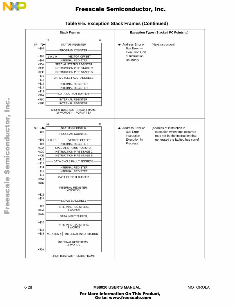
6-28 M68020 USER’S MANUAL MOTOROLA
Table 6-5. Exception Stack Frames (Continued)
Exception Types (Stacked PC Points to)Stack Frames
Address Error orBus Error —Execution Unitat InstructionBoundary
[Next instruction]SP
SP
INTERNAL INFORMATION
STATUS REGISTER
15 0
PROGRAM COUNTER
VECTOR OFFSET1 0 1 0+$06
+$02
INTERNAL REGISTER+$08SPECIAL STATUS REGISTER+$0AINSTRUCTION PIPE STAGE C+$0CINSTRUCTION PIPE STAGE B+$0E
+$10+$12
INTERNAL REGISTER+$14
INTERNAL REGISTER+$16+$18+$1A
INTERNAL REGISTER+$1C
DATA CYCLE FAULT ADDRESS
DATA OUTPUT BUFFER
INTERNAL REGISTER+$1E
STATUS REGISTER
15 0
PROGRAM COUNTER
VECTOR OFFSET1 0 1 1+$06
+$02
INTERNAL REGISTER+$08SPECIAL STATUS REGISTER+$0AINSTRUCTION PIPE STAGE C+$0CINSTRUCTION PIPE STAGE B+$0E
+$10+$12
INTERNAL REGISTER+$14
INTERNAL REGISTER+$16+$18
INTERNAL REGISTER,4 WORDS
DATA CYCLE FAULT ADDRESS
DATA OUTPUT BUFFER
+$22
+$2A
+$24
INTERNAL REGISTERS,2 WORDS
+$2C
+$30INTERNAL REGISTERS,
3 WORDS+$36+$38
INTERNAL REGISTERS,18 WORDS
+$5A
+$28
+$1A+$1C
VERSION #
DATA INPUT BUFFER
STAGE B ADDRESS
SHORT BUS FAULT STACK FRAME(16 WORDS) — FORMAT $A
Address Error orBus Error —InstructionExecution in Progress
[Address of instruction inexecution when fault occurred — may not be the instruction thatgenerated the faulted bus cycle]
LONG BUS FAULT STACK FRAME(46 WORDS) — FORMAT $B
Fre
esc
ale
Se
mic
on
du
cto
r, I
Freescale Semiconductor, Inc.
For More Information On This Product, Go to: www.freescale.com
nc
...

MOTOROLA M68020 USER’S MANUAL 7-1
SECTION 7COPROCESSOR INTERFACE DESCRIPTION
The M68000 family of general-purpose microprocessors provides a level of performancethat satisfies a wide range of computer applications. Special-purpose hardware, however,can often provide a higher level of performance for a specific application. The coprocessorconcept allows the capabilities and performance of a general-purpose processor to beenhanced for a particular application without encumbering the main processorarchitecture. A coprocessor can efficiently meet specific capability requirements that musttypically be implemented in software by a general-purpose processor. With a general-purpose main processor and the appropriate coprocessor(s), the processing capabilities ofa system can be tailored to a specific application.
The MC68020/EC020 supports the M68000 coprocessor interface described in thissection. This section is intended for designers who are implementing coprocessors tointerface with the MC68020/EC020.
The designer of a system that uses one or more Motorola coprocessors (the MC68881 orMC68882 floating-point coprocessor, for example) does not require a detailed knowledgeof the M68000 coprocessor interface. Motorola coprocessors conform to the interfacedescribed in this section. Typically, they implement a subset of the interface, and thatsubset is described in the coprocessor user's manual. These coprocessors executeMotorola-defined instructions that are described in the user's manual for eachcoprocessor.
7.1 INTRODUCTION
The distinction between standard peripheral hardware and an M68000 coprocessor isimportant from a programming model perspective. The programming model of the mainprocessor consists of the instruction set, register set, and memory map. An M68000coprocessor is a device or set of devices that communicates with the main processorthrough the protocol defined as the M68000 coprocessor interface. The programmingmodel for a coprocessor is different than that for a peripheral device. A coprocessor addsadditional instructions and generally additional registers and data types to theprogramming model that are not directly supported by the main processor architecture.The additional instructions are dedicated coprocessor instructions that utilize thecoprocessor capabilities. The necessary interactions between the main processor and thecoprocessor that provide a given service are transparent to the programmer. That is, theprogrammer does not need to know the specific communication protocol between themain processor and the coprocessor because this protocol is implemented in hardware.Thus, the coprocessor can provide capabilities to the user without appearing separatefrom the main processor.
Fre
esc
ale
Se
mic
on
du
cto
r, I
Freescale Semiconductor, Inc.
For More Information On This Product, Go to: www.freescale.com
nc
...
7-2 M68020 USER’S MANUAL MOTOROLA
In contrast, standard peripheral hardware is generally accessed through interfaceregisters mapped into the memory space of the main processor. To use the servicesprovided by the peripheral, the programmer accesses the peripheral registers withstandard processor instructions. While a peripheral could conceivably provide capabilitiesequivalent to a coprocessor for many applications, the programmer must implement thecommunication protocol between the main processor and the peripheral necessary to usethe peripheral hardware.
The communication protocol defined for the M68000 coprocessor interface is described in7.2 Coprocessor Instruction Types. The algorithms that implement the M68000coprocessor interface are provided in the microcode of the MC68020/EC020 and arecompletely transparent to the MC68020/EC020 programming model. For example,floating-point operations are not implemented in the MC68020/EC020 hardware. In asystem utilizing both the MC68020/EC020 and the MC68881 or MC68882 floating-pointcoprocessor, a programmer can use any of the instructions defined for the coprocessorwithout knowing that the actual computation is performed by the MC68881 or MC68882hardware.
7.1.1 Interface Features
The M68000 coprocessor interface design incorporates a number of flexible capabilities.The physical coprocessor interface uses the main processor external bus, which simplifiesthe interface since no special-purpose signals are involved. With the MC68020/EC020, acoprocessor uses the asynchronous bus transfer protocol. Since standard bus cyclestransfer information between the main processor and the coprocessor, the coprocessorcan be implemented in whatever technology is available to the coprocessor designer. Acoprocessor can be implemented as a VLSI device, as a separate system board, or evenas a separate computer system.
Since the main processor and a M68000 coprocessor can communicate using theasynchronous bus, they can operate at different clock frequencies. The system designercan choose the speeds of a main processor and coprocessor that provide the optimumperformance for a given system. Both the MC68881 and MC68882 floating-pointcoprocessors use the asynchronous bus handshake protocol.
The M68000 coprocessor interface also facilitates the design of coprocessors. Thecoprocessor designer must only conform to the coprocessor interface and does not needan extensive knowledge of the architecture of the main processor. Also, the mainprocessor can operate with a coprocessor without having explicit provisions made in themain processor for the capabilities of that coprocessor. This type of interface provides agreat deal of freedom in the implementation of a given coprocessor.
7.1.2 Concurrent Operation Support
The programming model for the M68000 family of microprocessors is based onsequential, nonconcurrent instruction execution, which implies that the instructions in agiven sequence must appear to be executed in the order in which they occur. To maintaina uniform programming model, any coprocessor extensions should also maintain the
Fre
esc
ale
Se
mic
on
du
cto
r, I
Freescale Semiconductor, Inc.
For More Information On This Product, Go to: www.freescale.com
nc
...
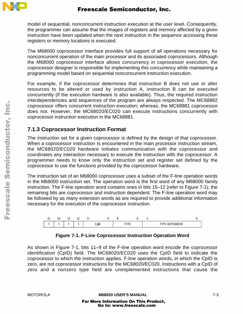
MOTOROLA M68020 USER’S MANUAL 7-3
model of sequential, nonconcurrent instruction execution at the user level. Consequently,the programmer can assume that the images of registers and memory affected by a giveninstruction have been updated when the next instruction in the sequence accessing theseregisters or memory locations is executed.
The M68000 coprocessor interface provides full support of all operations necessary fornonconcurrent operation of the main processor and its associated coprocessors. Althoughthe M68000 coprocessor interface allows concurrency in coprocessor execution, thecoprocessor designer is responsible for implementing this concurrency while maintaining aprogramming model based on sequential nonconcurrent instruction execution.
For example, if the coprocessor determines that instruction B does not use or alterresources to be altered or used by instruction A, instruction B can be executedconcurrently (if the execution hardware is also available). Thus, the required instructioninterdependencies and sequences of the program are always respected. The MC68882coprocessor offers concurrent instruction execution; whereas, the MC68881 coprocessordoes not. However, the MC68020/EC020 can execute instructions concurrently withcoprocessor instruction execution in the MC68881.
7.1.3 Coprocessor Instruction Format
The instruction set for a given coprocessor is defined by the design of that coprocessor.When a coprocessor instruction is encountered in the main processor instruction stream,the MC68020/EC020 hardware initiates communication with the coprocessor andcoordinates any interaction necessary to execute the instruction with the coprocessor. Aprogrammer needs to know only the instruction set and register set defined by thecoprocessor to use the functions provided by the coprocessor hardware.
The instruction set of an M68000 coprocessor uses a subset of the F-line operation wordsin the M68000 instruction set. The operation word is the first word of any M68000 familyinstruction. The F-line operation word contains ones in bits 15–12 (refer to Figure 7-1); theremaining bits are coprocessor and instruction dependent. The F-line operation word maybe followed by as many extension words as are required to provide additional informationnecessary for the execution of the coprocessor instruction.
15 0
1 1 1
14 13 12
1
11
CpID
9 8
TYPE
6 5
TYPE DEPENDENT
Figure 7-1. F-Line Coprocessor Instruction Operation Word
As shown in Figure 7-1, bits 11–9 of the F-line operation word encode the coprocessoridentification (CpID) field. The MC68020/EC020 uses the CpID field to indicate thecoprocessor to which the instruction applies. F-line operation words, in which the CpID iszero, are not coprocessor instructions for the MC68020/EC020. Instructions with a CpID ofzero and a nonzero type field are unimplemented instructions that cause the
Fre
esc
ale
Se
mic
on
du
cto
r, I
Freescale Semiconductor, Inc.
For More Information On This Product, Go to: www.freescale.com
nc
...

7-4 M68020 USER’S MANUAL MOTOROLA
MC68020/EC020 to begin exception processing. The MC68020/EC020 never generatescoprocessor interface bus cycles with the CpID equal to zero (except via the MOVESinstruction).
CpID codes of 000–101 are reserved for current and future Motorola coprocessors, andCpID codes of 110–111 are reserved for user-defined coprocessors. The Motorola CpIDcode of 001 designates the MC68881 or MC68882 floating-point coprocessor. By default,Motorola assemblers will use a CpID code of 001 when generating the instructionoperation codes for the MC68881 or MC68882.
The encoding of bits 8–0 of the coprocessor instruction operation word is dependent onthe particular instruction being implemented (refer to 7.2 Coprocessor InstructionTypes).
7.1.4 Coprocessor System Interface
The communication protocol between the main processor and coprocessor necessary toexecute a coprocessor instruction uses a group of interface registers, CIRs, residentwithin the coprocessor. By accessing one of the CIRs, the MC68020/EC020 hardwareinitiates coprocessor instructions. The coprocessor uses a set of response primitive codesand format codes defined for the M68000 coprocessor interface to communicate statusand service requests to the main processor through these registers. The CIRs are alsoused to pass operands between the main processor and the coprocessor. The CIR set,response primitives, and format codes are discussed in 7.3 Coprocessor InterfaceRegister Set and 7.4 Coprocessor Response Primitives.
7.1.4.1 COPROCESSOR CLASSIFICATION. M68000 coprocessors can be classified intotwo categories depending on their bus interface capabilities. The first category, non-DMAcoprocessors, consists of coprocessors that always operate as bus slaves. The secondcategory, DMA coprocessors, consists of coprocessors that operate as bus slaves whilecommunicating with the main processor across the coprocessor interface. Thesecoprocessors also have the ability to operate as bus masters, directly controlling thesystem bus.
If the operation of a coprocessor does not require a large portion of the available busbandwidth or has special requirements not directly satisfied by the main processor, thatcoprocessor can be efficiently implemented as a non-DMA coprocessor. Since non-DMAcoprocessors always operate as bus slaves, all external bus-related functions that thecoprocessor requires are performed by the main processor. The main processor transfersoperands from the coprocessor by reading the operand from the appropriate CIR and thenwriting the operand to a specified effective address with the appropriate address spacespecified on the FC2–FC0. Likewise, the main processor transfers operands to thecoprocessor by reading the operand from a specified effective address (and addressspace) and then writing that operand to the appropriate CIR using the coprocessorinterface. The bus interface circuitry of a coprocessor operating as a bus slave is not ascomplex as that of a device operating as a bus master.
Fre
esc
ale
Se
mic
on
du
cto
r, I
Freescale Semiconductor, Inc.
For More Information On This Product, Go to: www.freescale.com
nc
...
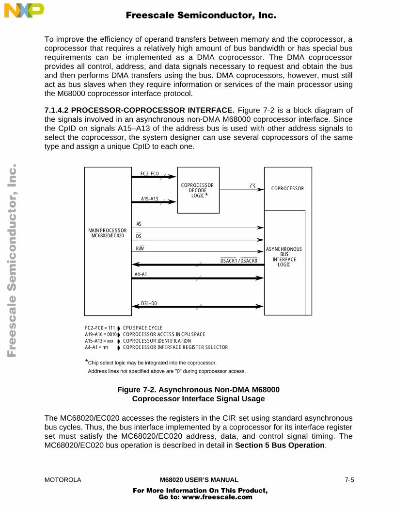
MOTOROLA M68020 USER’S MANUAL 7-5
To improve the efficiency of operand transfers between memory and the coprocessor, acoprocessor that requires a relatively high amount of bus bandwidth or has special busrequirements can be implemented as a DMA coprocessor. The DMA coprocessorprovides all control, address, and data signals necessary to request and obtain the busand then performs DMA transfers using the bus. DMA coprocessors, however, must stillact as bus slaves when they require information or services of the main processor usingthe M68000 coprocessor interface protocol.
7.1.4.2 PROCESSOR-COPROCESSOR INTERFACE. Figure 7-2 is a block diagram ofthe signals involved in an asynchronous non-DMA M68000 coprocessor interface. Sincethe CpID on signals A15–A13 of the address bus is used with other address signals toselect the coprocessor, the system designer can use several coprocessors of the sametype and assign a unique CpID to each one.
FC2–FC0
A19–A13
COPROCESSORDECODE
LOGIC
CS COPROCESSOR
ASYNCHRONOUSBUS
INTERFACELOGIC
AS
DS
R/W
A4–A1
D31–D0
DSACK1 / DSACK0
MAIN PROCESSORMC68020/EC020
FC2–FC0 = 111 A19–A16 = 0010 A15–A13 = xxx A4–A1 = rrrr
*Chip select logic may be integrated into the coprocessor.
Address lines not specified above are "0" during coprocessor access.
➧➧➧➧
*
CPU SPACE CYCLE COPROCESSOR ACCESS IN CPU SPACECOPROCESSOR IDENTIFICATIONCOPROCESSOR INFERFACE REGISTER SELECTOR
Figure 7-2. Asynchronous Non-DMA M68000Coprocessor Interface Signal Usage
The MC68020/EC020 accesses the registers in the CIR set using standard asynchronousbus cycles. Thus, the bus interface implemented by a coprocessor for its interface registerset must satisfy the MC68020/EC020 address, data, and control signal timing. TheMC68020/EC020 bus operation is described in detail in Section 5 Bus Operation.
Fre
esc
ale
Se
mic
on
du
cto
r, I
Freescale Semiconductor, Inc.
For More Information On This Product, Go to: www.freescale.com
nc
...
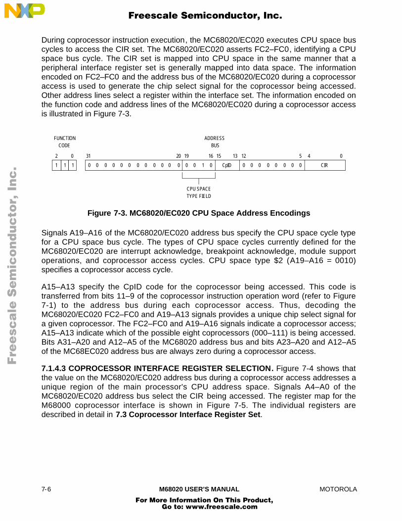
7-6 M68020 USER’S MANUAL MOTOROLA
During coprocessor instruction execution, the MC68020/EC020 executes CPU space buscycles to access the CIR set. The MC68020/EC020 asserts FC2–FC0, identifying a CPUspace bus cycle. The CIR set is mapped into CPU space in the same manner that aperipheral interface register set is generally mapped into data space. The informationencoded on FC2–FC0 and the address bus of the MC68020/EC020 during a coprocessoraccess is used to generate the chip select signal for the coprocessor being accessed.Other address lines select a register within the interface set. The information encoded onthe function code and address lines of the MC68020/EC020 during a coprocessor accessis illustrated in Figure 7-3.
0
CIRCpID0 10000000000001 0 000000
4512131519203102
000
16
11
FUNCTIONCODE
ADDRESSBUS
CPU SPACETYPE FIELD
Figure 7-3. MC68020/EC020 CPU Space Address Encodings
Signals A19–A16 of the MC68020/EC020 address bus specify the CPU space cycle typefor a CPU space bus cycle. The types of CPU space cycles currently defined for theMC68020/EC020 are interrupt acknowledge, breakpoint acknowledge, module supportoperations, and coprocessor access cycles. CPU space type $2 (A19–A16 = 0010)specifies a coprocessor access cycle.
A15–A13 specify the CpID code for the coprocessor being accessed. This code istransferred from bits 11–9 of the coprocessor instruction operation word (refer to Figure7-1) to the address bus during each coprocessor access. Thus, decoding theMC68020/EC020 FC2–FC0 and A19–A13 signals provides a unique chip select signal fora given coprocessor. The FC2–FC0 and A19–A16 signals indicate a coprocessor access;A15–A13 indicate which of the possible eight coprocessors (000–111) is being accessed.Bits A31–A20 and A12–A5 of the MC68020 address bus and bits A23–A20 and A12–A5of the MC68EC020 address bus are always zero during a coprocessor access.
7.1.4.3 COPROCESSOR INTERFACE REGISTER SELECTION. Figure 7-4 shows thatthe value on the MC68020/EC020 address bus during a coprocessor access addresses aunique region of the main processor's CPU address space. Signals A4–A0 of theMC68020/EC020 address bus select the CIR being accessed. The register map for theM68000 coprocessor interface is shown in Figure 7-5. The individual registers aredescribed in detail in 7.3 Coprocessor Interface Register Set.
Fre
esc
ale
Se
mic
on
du
cto
r, I
Freescale Semiconductor, Inc.
For More Information On This Product, Go to: www.freescale.com
nc
...
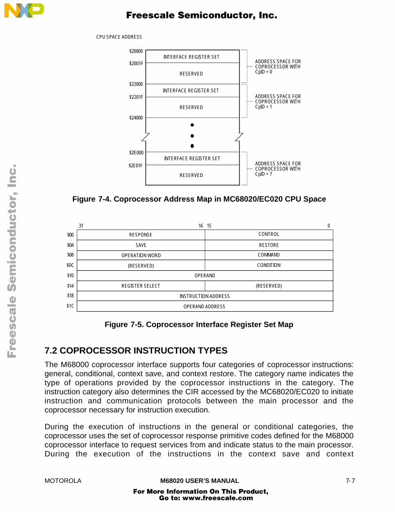
MOTOROLA M68020 USER’S MANUAL 7-7
INTERFACE REGISTER SET
RESERVED
INTERFACE REGISTER SET
RESERVED
INTERFACE REGISTER SET
RESERVED
CPU SPACE ADDRESS
$20000
$2001F
$22000
$2201F
$24000
$2E000
$2E01F
ADDRESS SPACE FORCOPROCESSOR WITHCpID = 0
ADDRESS SPACE FORCOPROCESSOR WITHCpID = 1
ADDRESS SPACE FORCOPROCESSOR WITHCpID = 7
Figure 7-4. Coprocessor Address Map in MC68020/EC020 CPU Space
31 15 0
$00
$04
$08
$0C
$10
$14
$18
$1C
OPERAND
(RESERVED)
INSTRUCTION ADDRESS
OPERAND ADDRESS
REGISTER SELECT
CONDITION(RESERVED)
COMMANDOPERATION WORD
RESTORESAVE
CONTROLRESPONSE
16
Figure 7-5. Coprocessor Interface Register Set Map
7.2 COPROCESSOR INSTRUCTION TYPES
The M68000 coprocessor interface supports four categories of coprocessor instructions:general, conditional, context save, and context restore. The category name indicates thetype of operations provided by the coprocessor instructions in the category. Theinstruction category also determines the CIR accessed by the MC68020/EC020 to initiateinstruction and communication protocols between the main processor and thecoprocessor necessary for instruction execution.
During the execution of instructions in the general or conditional categories, thecoprocessor uses the set of coprocessor response primitive codes defined for the M68000coprocessor interface to request services from and indicate status to the main processor.During the execution of the instructions in the context save and context
Fre
esc
ale
Se
mic
on
du
cto
r, I
Freescale Semiconductor, Inc.
For More Information On This Product, Go to: www.freescale.com
nc
...
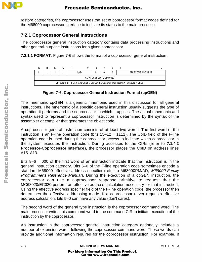
7-8 M68020 USER’S MANUAL MOTOROLA
restore categories, the coprocessor uses the set of coprocessor format codes defined forthe M68000 coprocessor interface to indicate its status to the main processor.
7.2.1 Coprocessor General Instructions
The coprocessor general instruction category contains data processing instructions andother general-purpose instructions for a given coprocessor.
7.2.1.1 FORMAT. Figure 7-6 shows the format of a coprocessor general instruction.
COPROCESSOR COMMAND
1
15
1
14
1
13
1
12 11
CpID
9
0
8
0
7
0
6 5
EFFECTIVE ADDRESS
0
OPTIONAL EFFECTIVE ADDRESS OR COPROCESSOR-DEFINED EXTENSION WORDS
Figure 7-6. Coprocessor General Instruction Format (cpGEN)
The mnemonic cpGEN is a generic mnemonic used in this discussion for all generalinstructions. The mnemonic of a specific general instruction usually suggests the type ofoperation it performs and the coprocessor to which it applies. The actual mnemonic andsyntax used to represent a coprocessor instruction is determined by the syntax of theassembler or compiler that generates the object code.
A coprocessor general instruction consists of at least two words. The first word of theinstruction is an F-line operation code (bits 15–12 = 1111). The CpID field of the F-lineoperation code is used during the coprocessor access to indicate which coprocessor inthe system executes the instruction. During accesses to the CIRs (refer to 7.1.4.2Processor-Coprocessor Interface), the processor places the CpID on address linesA15–A13.
Bits 8–6 = 000 of the first word of an instruction indicate that the instruction is in thegeneral instruction category. Bits 5–0 of the F-line operation code sometimes encode astandard M68000 effective address specifier (refer to M68000PM/AD, M68000 FamilyProgrammer’s Reference Manual). During the execution of a cpGEN instruction, thecoprocessor can use a coprocessor response primitive to request that theMC68020/EC020 perform an effective address calculation necessary for that instruction.Using the effective address specifier field of the F-line operation code, the processor thendetermines the effective addressing mode. If a coprocessor never requests effectiveaddress calculation, bits 5–0 can have any value (don't cares).
The second word of the general type instruction is the coprocessor command word. Themain processor writes this command word to the command CIR to initiate execution of theinstruction by the coprocessor.
An instruction in the coprocessor general instruction category optionally includes anumber of extension words following the coprocessor command word. These words canprovide additional information required for the coprocessor instruction. For example, if
Fre
esc
ale
Se
mic
on
du
cto
r, I
Freescale Semiconductor, Inc.
For More Information On This Product, Go to: www.freescale.com
nc
...

MOTOROLA M68020 USER’S MANUAL 7-9
the coprocessor requests that the MC68020/EC020 calculate an effective address duringcoprocessor instruction execution, information required for the calculation must beincluded in the instruction format as effective address extension words.
7.2.1.2 PROTOCOL. The execution of a cpGEN instruction follows the protocol shown inFigure 7-7. The main processor initiates communication with the coprocessor by writingthe instruction command word to the command CIR. The coprocessor decodes thecommand word to begin processing the cpGEN instruction. Coprocessor designdetermines the interpretation of the coprocessor command word; the MC68020/EC020does not attempt to decode it.
While the coprocessor is executing an instruction, it requests any required services fromand communicates status to the main processor by placing coprocessor responseprimitive codes in the response CIR. After writing to the command CIR, the mainprocessor reads the response CIR and responds appropriately. When the coprocessorhas completed the execution of an instruction or no longer needs the services of the mainprocessor to execute the instruction, it provides a response to release the main processor.The main processor can then execute the next instruction in the instruction stream.However, if a trace exception is pending, the MC68020/EC020 does not terminatecommunication with the coprocessor until the coprocessor indicates that it has completedall processing associated with the cpGEN instruction (refer to 7.5.2.5 Trace Exceptions).
The coprocessor interface protocol shown in Figure 7-7 allows the coprocessor to definethe operation of each coprocessor general type instruction. That is, the main processorinitiates the instruction execution by writing the instruction command word to thecommand CIR and by reading the response CIR to determine its next action. Theexecution of the coprocessor instruction is then defined by the internal operation of thecoprocessor and by its use of response primitives to request services from the mainprocessor. This instruction protocol allows a wide range of operations to be implementedin the general instruction category.
Fre
esc
ale
Se
mic
on
du
cto
r, I
Freescale Semiconductor, Inc.
For More Information On This Product, Go to: www.freescale.com
nc
...
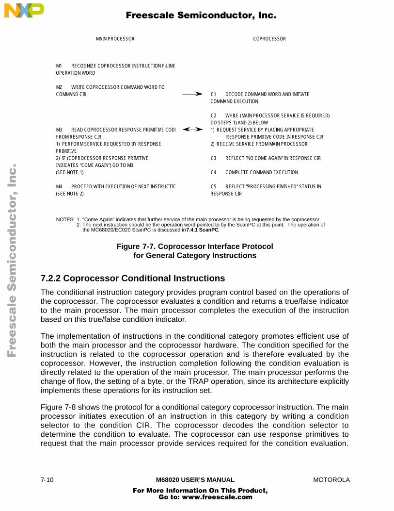
7-10 M68020 USER’S MANUAL MOTOROLA
M1 RECOGNIZE COPROCESSOR INSTRUCTION F-LINEOPERATION WORD
M2 WRITE COPROCESSOR COMMAND WORD TOCOMMAND CIR
M3 READ COPROCESSOR RESPONSE PRIMITIVE CODEFROM RESPONSE CIR1) PERFORM SERVICE REQUESTED BY RESPONSEPRIMITIVE2) IF (COPROCESSOR RESPONSE PRIMITIVEINDICATES "COME AGAIN") GO TO M3(SEE NOTE 1)
M4 PROCEED WITH EXECUTION OF NEXT INSTRUCTION(SEE NOTE 2)
C1 DECODE COMMAND WORD AND INITIATECOMMAND EXECUTION
C2 WHILE (MAIN PROCESSOR SERVICE IS REQUIRED)DO STEPS 1) AND 2) BELOW1) REQUEST SERVICE BY PLACING APPROPRIATE
RESPONSE PRIMITIVE CODE IN RESPONSE CIR2) RECEIVE SERVICE FROM MAIN PROCESSOR
C3 REFLECT "NO COME AGAIN" IN RESPONSE CIR
C4 COMPLETE COMMAND EXECUTION
C5 REFLECT "PROCESSING FINISHED" STATUS INRESPONSE CIR
MAIN PROCESSOR COPROCESSOR
NOTES: 1. "Come Again" indicates that further service of the main processor is being requested by the coprocessor.2. The next instruction should be the operation word pointed to by the ScanPC at this point. The operation ofthe MC68020/EC020 ScanPC is discussed in 7.4.1 ScanPC.
Figure 7-7. Coprocessor Interface Protocolfor General Category Instructions
7.2.2 Coprocessor Conditional Instructions
The conditional instruction category provides program control based on the operations ofthe coprocessor. The coprocessor evaluates a condition and returns a true/false indicatorto the main processor. The main processor completes the execution of the instructionbased on this true/false condition indicator.
The implementation of instructions in the conditional category promotes efficient use ofboth the main processor and the coprocessor hardware. The condition specified for theinstruction is related to the coprocessor operation and is therefore evaluated by thecoprocessor. However, the instruction completion following the condition evaluation isdirectly related to the operation of the main processor. The main processor performs thechange of flow, the setting of a byte, or the TRAP operation, since its architecture explicitlyimplements these operations for its instruction set.
Figure 7-8 shows the protocol for a conditional category coprocessor instruction. The mainprocessor initiates execution of an instruction in this category by writing a conditionselector to the condition CIR. The coprocessor decodes the condition selector todetermine the condition to evaluate. The coprocessor can use response primitives torequest that the main processor provide services required for the condition evaluation.
Fre
esc
ale
Se
mic
on
du
cto
r, I
Freescale Semiconductor, Inc.
For More Information On This Product, Go to: www.freescale.com
nc
...
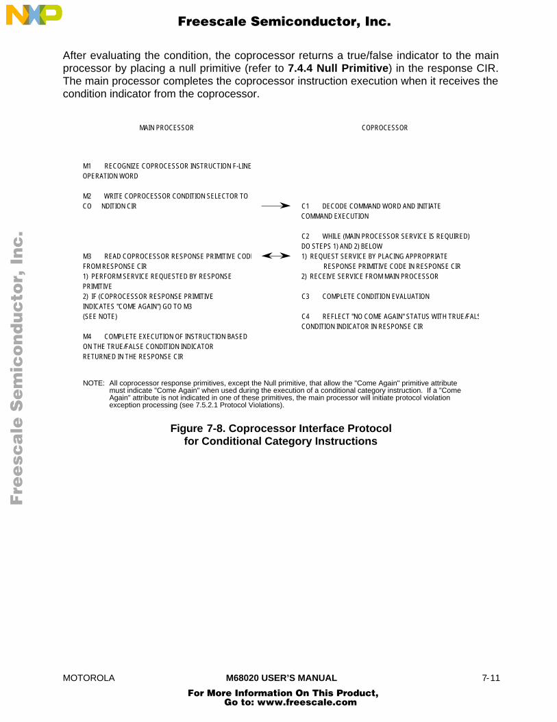
MOTOROLA M68020 USER’S MANUAL 7-11
After evaluating the condition, the coprocessor returns a true/false indicator to the mainprocessor by placing a null primitive (refer to 7.4.4 Null Primitive) in the response CIR.The main processor completes the coprocessor instruction execution when it receives thecondition indicator from the coprocessor.
M1 RECOGNIZE COPROCESSOR INSTRUCTION F-LINEOPERATION WORD
M2 WRITE COPROCESSOR CONDITION SELECTOR TOCO NDITION CIR
M3 READ COPROCESSOR RESPONSE PRIMITIVE CODEFROM RESPONSE CIR1) PERFORM SERVICE REQUESTED BY RESPONSEPRIMITIVE2) IF (COPROCESSOR RESPONSE PRIMITIVEINDICATES "COME AGAIN") GO TO M3(SEE NOTE)
M4 COMPLETE EXECUTION OF INSTRUCTION BASED ON THE TRUE/FALSE CONDITION INDICATORRETURNED IN THE RESPONSE CIR
C1 DECODE COMMAND WORD AND INITIATECOMMAND EXECUTION
C2 WHILE (MAIN PROCESSOR SERVICE IS REQUIRED)DO STEPS 1) AND 2) BELOW1) REQUEST SERVICE BY PLACING APPROPRIATE
RESPONSE PRIMITIVE CODE IN RESPONSE CIR2) RECEIVE SERVICE FROM MAIN PROCESSOR
C3 COMPLETE CONDITION EVALUATION
C4 REFLECT "NO COME AGAIN" STATUS WITH TRUE/FALSECONDITION INDICATOR IN RESPONSE CIR
MAIN PROCESSOR COPROCESSOR
NOTE: All coprocessor response primitives, except the Null primitive, that allow the "Come Again" primitive attribute must indicate "Come Again" when used during the execution of a conditional category instruction. If a "Come Again" attribute is not indicated in one of these primitives, the main processor will initiate protocol violation exception processing (see 7.5.2.1 Protocol Violations).
Figure 7-8. Coprocessor Interface Protocolfor Conditional Category Instructions
Fre
esc
ale
Se
mic
on
du
cto
r, I
Freescale Semiconductor, Inc.
For More Information On This Product, Go to: www.freescale.com
nc
...

7-12 M68020 USER’S MANUAL MOTOROLA
7.2.2.1 BRANCH ON COPROCESSOR CONDITION INSTRUCTION. The conditionalinstruction category includes two formats of the M68000 family branch instruction. Theseinstructions branch on conditions related to the coprocessor operation. They executesimilarly to the conditional branch instructions provided in the M68000 family instructionset.
7.2.2.1.1 Format. Figure 7-9 shows the format of the branch on coprocessor conditioninstruction that provides a word-length displacement. Figure 7-10 shows the format of thisinstruction that includes a long-word displacement.
DISPLACEMENT
1
15
1
14
1
13
1
12 11
CpID
9
0
8
1
7
0
6 5
CONDITION SELECTOR
0
OPTIONAL COPROCESSOR-DEFINED EXTENSION WORDS
Figure 7-9. Branch on Coprocessor ConditionInstruction Format (cpBcc.W)
DISPLACEMENT — HIGH
1
15
1
14
1
13
1
12 11
CpID
9
0
8
1
7
1
6 5
CONDITION SELECTOR
0
OPTIONAL COPROCESSOR-DEFINED EXTENSION WORDS
DISPLACEMENT — LOW
Figure 7-10. Branch on Coprocessor ConditionInstruction Format (cpBcc.L)
The first word of the branch on coprocessor condition instruction is the F-line operationword. Bits 15–12 = 1111 and bits 11–9 contain the CpID code of the coprocessor that is toevaluate the condition. The value in bits 8–6 identifies either the word or the long-worddisplacement format of the branch instruction, which is specified by the cpBcc.W orcpBcc.L mnemonic, respectively. Bits 5–0 of the F-line operation word contain thecoprocessor condition selector field. The MC68020/EC020 writes the entire operationword to the condition CIR to initiate execution of the branch instruction by thecoprocessor. The coprocessor uses bits 5–0 to determine which condition to evaluate.
If the coprocessor requires additional information to evaluate the condition, the branchinstruction format can include this information in extension words. Following the F-lineoperation word, the number of extension words is determined by the coprocessor design.The final word(s) of the cpBcc instruction format contains the displacement used by themain processor to calculate the destination address when the branch is taken.
7.2.2.1.2 Protocol. Figure 7-8 shows the protocol for the cpBcc.L and cpBcc.Winstructions. The main processor initiates the instruction by writing the F-line operationword to the condition CIR to transfer the condition selector to the coprocessor. The main
Fre
esc
ale
Se
mic
on
du
cto
r, I
Freescale Semiconductor, Inc.
For More Information On This Product, Go to: www.freescale.com
nc
...

MOTOROLA M68020 USER’S MANUAL 7-13
processor then reads the response CIR to determine its next action. The coprocessor can
Fre
esc
ale
Se
mic
on
du
cto
r, I
Freescale Semiconductor, Inc.
For More Information On This Product, Go to: www.freescale.com
nc
...
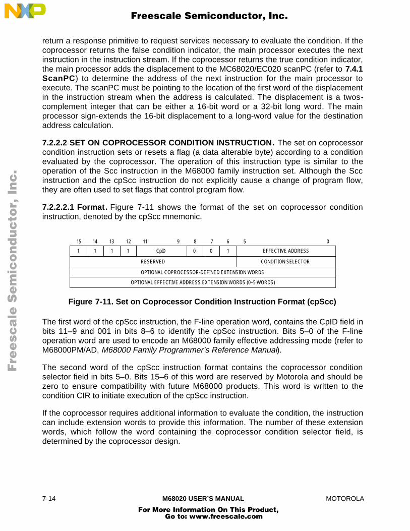
7-14 M68020 USER’S MANUAL MOTOROLA
return a response primitive to request services necessary to evaluate the condition. If thecoprocessor returns the false condition indicator, the main processor executes the nextinstruction in the instruction stream. If the coprocessor returns the true condition indicator,the main processor adds the displacement to the MC68020/EC020 scanPC (refer to 7.4.1ScanPC) to determine the address of the next instruction for the main processor toexecute. The scanPC must be pointing to the location of the first word of the displacementin the instruction stream when the address is calculated. The displacement is a twos-complement integer that can be either a 16-bit word or a 32-bit long word. The mainprocessor sign-extends the 16-bit displacement to a long-word value for the destinationaddress calculation.
7.2.2.2 SET ON COPROCESSOR CONDITION INSTRUCTION. The set on coprocessorcondition instruction sets or resets a flag (a data alterable byte) according to a conditionevaluated by the coprocessor. The operation of this instruction type is similar to theoperation of the Scc instruction in the M68000 family instruction set. Although the Sccinstruction and the cpScc instruction do not explicitly cause a change of program flow,they are often used to set flags that control program flow.
7.2.2.2.1 Format. Figure 7-11 shows the format of the set on coprocessor conditioninstruction, denoted by the cpScc mnemonic.
1
15
1
14
1
13
1
12 11
CpID
9
0
8
0
7
1
6 5
EFFECTIVE ADDRESS
0
OPTIONAL COPROCESSOR-DEFINED EXTENSION WORDS
OPTIONAL EFFECTIVE ADDRESS EXTENSION WORDS (0–5 WORDS)
CONDITION SELECTORRESERVED
Figure 7-11. Set on Coprocessor Condition Instruction Format (cpScc)
The first word of the cpScc instruction, the F-line operation word, contains the CpID field inbits 11–9 and 001 in bits 8–6 to identify the cpScc instruction. Bits 5–0 of the F-lineoperation word are used to encode an M68000 family effective addressing mode (refer toM68000PM/AD, M68000 Family Programmer’s Reference Manual).
The second word of the cpScc instruction format contains the coprocessor conditionselector field in bits 5–0. Bits 15–6 of this word are reserved by Motorola and should bezero to ensure compatibility with future M68000 products. This word is written to thecondition CIR to initiate execution of the cpScc instruction.
If the coprocessor requires additional information to evaluate the condition, the instructioncan include extension words to provide this information. The number of these extensionwords, which follow the word containing the coprocessor condition selector field, isdetermined by the coprocessor design.
Fre
esc
ale
Se
mic
on
du
cto
r, I
Freescale Semiconductor, Inc.
For More Information On This Product, Go to: www.freescale.com
nc
...
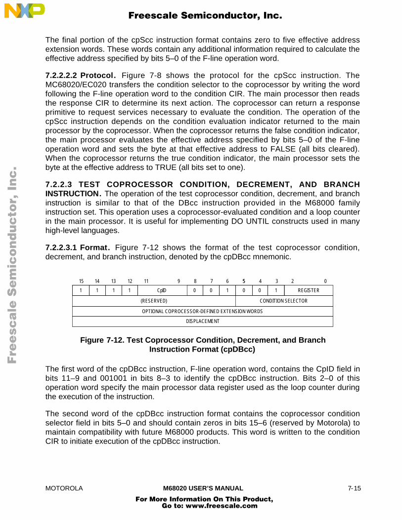
MOTOROLA M68020 USER’S MANUAL 7-15
The final portion of the cpScc instruction format contains zero to five effective addressextension words. These words contain any additional information required to calculate theeffective address specified by bits 5–0 of the F-line operation word.
7.2.2.2.2 Protocol. Figure 7-8 shows the protocol for the cpScc instruction. TheMC68020/EC020 transfers the condition selector to the coprocessor by writing the wordfollowing the F-line operation word to the condition CIR. The main processor then readsthe response CIR to determine its next action. The coprocessor can return a responseprimitive to request services necessary to evaluate the condition. The operation of thecpScc instruction depends on the condition evaluation indicator returned to the mainprocessor by the coprocessor. When the coprocessor returns the false condition indicator,the main processor evaluates the effective address specified by bits 5–0 of the F-lineoperation word and sets the byte at that effective address to FALSE (all bits cleared).When the coprocessor returns the true condition indicator, the main processor sets thebyte at the effective address to TRUE (all bits set to one).
7.2.2.3 TEST COPROCESSOR CONDITION, DECREMENT, AND BRANCHINSTRUCTION. The operation of the test coprocessor condition, decrement, and branchinstruction is similar to that of the DBcc instruction provided in the M68000 familyinstruction set. This operation uses a coprocessor-evaluated condition and a loop counterin the main processor. It is useful for implementing DO UNTIL constructs used in manyhigh-level languages.
7.2.2.3.1 Format. Figure 7-12 shows the format of the test coprocessor condition,decrement, and branch instruction, denoted by the cpDBcc mnemonic.
1
15
1
14
1
13
1
12 11
CpID
9
0
8
0
7
1
6 5
REGISTER
0
OPTIONAL COPROCESSOR-DEFINED EXTENSION WORDS
DISPLACEMENT
CONDITION SELECTOR
0
5
0
4
1
3 2
(RESERVED)
Figure 7-12. Test Coprocessor Condition, Decrement, and BranchInstruction Format (cpDBcc)
The first word of the cpDBcc instruction, F-line operation word, contains the CpID field inbits 11–9 and 001001 in bits 8–3 to identify the cpDBcc instruction. Bits 2–0 of thisoperation word specify the main processor data register used as the loop counter duringthe execution of the instruction.
The second word of the cpDBcc instruction format contains the coprocessor conditionselector field in bits 5–0 and should contain zeros in bits 15–6 (reserved by Motorola) tomaintain compatibility with future M68000 products. This word is written to the conditionCIR to initiate execution of the cpDBcc instruction.
Fre
esc
ale
Se
mic
on
du
cto
r, I
Freescale Semiconductor, Inc.
For More Information On This Product, Go to: www.freescale.com
nc
...

7-16 M68020 USER’S MANUAL MOTOROLA
If the coprocessor requires additional information to evaluate the condition, the cpDBccinstruction can include this information in extension words. These extension words followthe word containing the coprocessor condition selector field in the cpDBcc instructionformat.
The last word of the instruction contains the displacement for the cpDBcc instruction. Thisdisplacement is a twos-complement 16-bit value that is sign-extended to long-word sizewhen it is used in a destination address calculation.
7.2.2.3.2 Protocol. Figure 7-8 shows the protocol for the cpDBcc instructions. TheMC68020/EC020 transfers the condition selector to the coprocessor by writing the wordfollowing the operation word to the condition CIR. The main processor then reads theresponse CIR to determine its next action. The coprocessor can use a response primitiveto request any services necessary to evaluate the condition. If the coprocessor returns thetrue condition indicator, the main processor executes the next instruction in the instructionstream. If the coprocessor returns the false condition indicator, the main processordecrements the low-order word of the register specified by bits 2–0 of the F-line operationword. If this register contains minus one (–1) after being decremented, the main processorexecutes the next instruction in the instruction stream. If the register does not containminus one (–1) after being decremented, the main processor branches to the destinationaddress to continue instruction execution.
The MC68020/EC020 adds the displacement to the scanPC (refer to 7.4.1 ScanPC) todetermine the address of the next instruction. The scanPC must point to the 16-bitdisplacement in the instruction stream when the destination address is calculated.
7.2.2.4 TRAP ON COPROCESSOR CONDITION INSTRUCTION. The trap oncoprocessor condition instruction allows the programmer to initiate exception processingbased on conditions related to the coprocessor operation.
7.2.2.4.1 Format. Figure 7-13 shows the format of the trap on coprocessor conditioninstruction, denoted by the cpTRAPcc mnemonic.
1
15
1
14
1
13
1
12 11
CpID
9
0
8
0
7
1
6 5
OPMODE
0
OPTIONAL COPROCESSOR-DEFINED EXTENSION WORDS
OPTIONAL WORD
CONDITION SELECTOR
1
5
1
4
1
3 2
(RESERVED)
OR LONG-WORD OPERAND
Figure 7-13. Trap on Coprocessor ConditionInstruction Format (cpTRAPcc)
The first word of the cpTRAPcc instruction, the F-line operation word contains the CpIDfield in bits 11–9 and 001111 in bits 8–3 to identify the cpTRAPcc instruction. Bits 2–0 ofthe cpTRAPcc F-line operation word specify the opmode, which selects the instructionformat. The instruction format can include zero, one, or two operand words.
Fre
esc
ale
Se
mic
on
du
cto
r, I
Freescale Semiconductor, Inc.
For More Information On This Product, Go to: www.freescale.com
nc
...

MOTOROLA M68020 USER’S MANUAL 7-17
The second word of the cpTRAPcc instruction format contains the coprocessor conditionselector in bits 5–0 and should contain zeros in bits 15–6 (these bits are reserved byMotorola) to maintain compatibility with future M68000 products. This word is written to thecondition CIR to initiate execution of the cpTRAPcc instruction.
If the coprocessor requires additional information to evaluate a condition, the instructioncan include this information in extension words. These extension words follow the wordcontaining the coprocessor condition selector field in the cpTRAPcc instruction format.
The operand words of the cpTRAPcc F-line operation word follow the coprocessor-definedextension words. These operand words are not explicitly used by the MC68020/EC020,but can be used to contain information referenced by the cpTRAPcc exception handlingroutines. The valid encodings for bits 2–0 of the F-line operation word and thecorresponding numbers of operand words are listed in Table 7-1. Other encodings ofthese bits are invalid for the cpTRAPcc instruction.
Table 7-1. cpTRAPcc Opmode Encodings
Opmode Operand Words in Instruction Format
010 One
011 Two
100 Zero
7.2.2.4.2 Protocol. Figure 7-8 shows the protocol for the cpTRAPcc instructions. TheMC68020/EC020 transfers the condition selector to the coprocessor by writing the wordfollowing the operation word to the condition CIR. The main processor then reads theresponse CIR to determine its next action. The coprocessor can return a responseprimitive to request any services necessary to evaluate the condition. If the coprocessorreturns the true condition indicator, the main processor initiates exception processing forthe cpTRAPcc exception (refer to 7.5.2.4 cpTRAPcc Instruction Traps). If thecoprocessor returns the false condition indicator, the main processor executes the nextinstruction in the instruction stream.
7.2.3 Coprocessor Context Save and Restore Instructions
The coprocessor context save and context restore instruction categories in the M68000coprocessor interface support multitasking programming environments. In a multitaskingenvironment, the context of a coprocessor may need to be changed asynchronously withrespect to the operation of that coprocessor. That is, the coprocessor may be interruptedat any point in the execution of an instruction in the general or conditional category tobegin context change operations.
In contrast to the general and conditional instruction categories, the context save andcontext restore instruction categories do not use the coprocessor response primitives. Aset of format codes defined by the M68000 coprocessor interface communicates status
Fre
esc
ale
Se
mic
on
du
cto
r, I
Freescale Semiconductor, Inc.
For More Information On This Product, Go to: www.freescale.com
nc
...

7-18 M68020 USER’S MANUAL MOTOROLA
information to the main processor during the execution of these instructions. Thesecoprocessor format codes are discussed in detail in 7.2.3.2 Coprocessor Format Words.
7.2.3.1 COPROCESSOR INTERNAL STATE FRAMES. The context save (cpSAVE) andcontext restore (cpRESTORE) instructions transfer an internal coprocessor state framebetween memory and a coprocessor. This internal coprocessor state frame represents thestate of coprocessor operations. Using the cpSAVE and cpRESTORE instructions, it ispossible to interrupt coprocessor operation, save the context associated with the currentoperation, and initiate coprocessor operations with a new context.
A cpSAVE instruction stores a coprocessor internal state frame as a sequence of long-word entries in memory. Figure 7-14 shows the format of a coprocessor state frame. Theformat and length fields of the coprocessor state frame format comprise the format word.During execution of the cpSAVE instruction, the MC68020/EC020 calculates the stateframe effective address from information in the operation word of the instruction andstores a format word at this effective address. The processor writes the long words thatform the coprocessor state frame to descending memory addresses, beginning with theaddress specified by the sum of the effective address and the length field multiplied byfour. During execution of the cpRESTORE instruction, the MC68020/EC020 reads thestate frame from ascending addresses beginning with the effective address specified inthe instruction operation word.
31
FORMAT
24 23
LENGTH
16 15
(UNUSED, RESERVED)
0
COPROCESSOR-DEPENDENT INFORMATION
0
SAVEORDER
0
RESTOREORDER
n 1
n–1 2
n–2 3
1 n
Figure 7-14. Coprocessor State Frame Format in Memory
The processor stores the coprocessor format word at the lowest address of the stateframe in memory, and this word is the first word transferred for both the cpSAVE andcpRESTORE instructions. The word following the format word does not containinformation relevant to the coprocessor state frame, but serves to keep the information inthe state frame a multiple of four bytes in size. The number of entries following the formatword (at higher addresses) is determined by the format word length for a givencoprocessor state.
Fre
esc
ale
Se
mic
on
du
cto
r, I
Freescale Semiconductor, Inc.
For More Information On This Product, Go to: www.freescale.com
nc
...
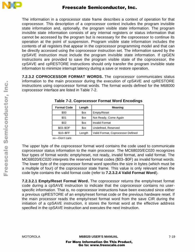
MOTOROLA M68020 USER’S MANUAL 7-19
The information in a coprocessor state frame describes a context of operation for thatcoprocessor. This description of a coprocessor context includes the program invisiblestate information and, optionally, the program visible state information. The programinvisible state information consists of any internal registers or status information thatcannot be accessed by the program but is necessary for the coprocessor to continue itsoperation at the point of suspension. Program visible state information includes thecontents of all registers that appear in the coprocessor programming model and that canbe directly accessed using the coprocessor instruction set. The information saved by thecpSAVE instruction must include the program invisible state information. If cpGENinstructions are provided to save the program visible state of the coprocessor, thecpSAVE and cpRESTORE instructions should only transfer the program invisible stateinformation to minimize interrupt latency during a save or restore operation.
7.2.3.2 COPROCESSOR FORMAT WORDS. The coprocessor communicates statusinformation to the main processor during the execution of cpSAVE and cpRESTOREinstructions using coprocessor format words. The format words defined for the M68000coprocessor interface are listed in Table 7-2.
Table 7-2. Coprocessor Format Word Encodings
Format Code Length Meaning
$00 $xx Empty/Reset
$01 $xx Not Ready, Come Again
$02 $xx Invalid Format
$03–$OF $xx Undefined, Reserved
$10–$FF Length Valid Format, Coprocessor Defined
xx—Don’t care
The upper byte of the coprocessor format word contains the code used to communicatecoprocessor status information to the main processor. The MC68020/EC020 recognizesfour types of format words: empty/reset, not ready, invalid format, and valid format. TheMC68020/EC020 interprets the reserved format codes ($03–$0F) as invalid format words.The lower byte of the coprocessor format word specifies the size in bytes (which must bea multiple of four) of the coprocessor state frame. This value is only relevant when thecode byte contains the valid format code (refer to 7.2.3.2.4 Valid Format Word).
7.2.3.2.1 Empty/Reset Format Word. The coprocessor returns the empty/reset formatcode during a cpSAVE instruction to indicate that the coprocessor contains no user-specific information. That is, no coprocessor instructions have been executed since eithera previous cpRESTORE of an empty/reset format code or the previous hardware reset. Ifthe main processor reads the empty/reset format word from the save CIR during theinitiation of a cpSAVE instruction, it stores the format word at the effective addressspecified in the cpSAVE instruction and executes the next instruction.
Fre
esc
ale
Se
mic
on
du
cto
r, I
Freescale Semiconductor, Inc.
For More Information On This Product, Go to: www.freescale.com
nc
...
7-20 M68020 USER’S MANUAL MOTOROLA
When the main processor reads the empty/reset format word from memory during theexecution of the cpRESTORE instruction, it writes the format word to the restore CIR. Themain processor then reads the restore CIR and, if the coprocessor returns the empty/resetformat word, executes the next instruction. The main processor can then initialize thecoprocessor by writing the empty/reset format code to restore the CIR. When thecoprocessor receives the empty/reset format code, it terminates any current operationsand waits for the main processor to initiate the next coprocessor instruction. In particular,after the cpRESTORE of the empty/reset format word, the execution of a cpSAVE shouldcause the empty/reset format word to be returned when a cpSAVE instruction is executedbefore any other coprocessor instructions. Thus, an empty/reset state frame consists onlyof the format word and the following reserved word in memory (refer to Figure 7-14).
7.2.3.2.2 Not-Ready Format Word. When the main processor initiates a cpSAVEinstruction by reading the save CIR, the coprocessor can delay the save operation byreturning a not-ready format word. The main processor then services any pendinginterrupts and reads the save CIR again. The not-ready format word delays the saveoperation until the coprocessor is ready to save its internal state. The cpSAVE instructioncan suspend execution of a general or conditional coprocessor instruction; thecoprocessor can resume execution of the suspended instruction when the appropriatestate is restored with a cpRESTORE. If no further main processor services are required tocomplete coprocessor instruction execution, it may be more efficient to complete theinstruction and thus reduce the size of the saved state. The coprocessor designer shouldconsider the efficiency of completing the instruction or of suspending and later resumingthe instruction when the main processor executes a cpSAVE instruction.
When the main processor initiates a cpRESTORE instruction by writing a format word tothe restore CIR, the coprocessor should usually terminate any current operations andrestore the state frame supplied by the main processor. Thus, the not-ready format wordshould usually not be returned by the coprocessor during the execution of a cpRESTOREinstruction. If the coprocessor must delay the cpRESTORE operation for any reason, itcan return the not-ready format word when the main processor reads the restore CIR. Ifthe main processor reads the not-ready format word from the restore CIR during thecpRESTORE instruction, it reads the restore CIR again without servicing any pendinginterrupts.
7.2.3.2.3 Invalid Format Word. When the format word placed in the restore CIR to initiatea cpRESTORE instruction does not describe a valid coprocessor state frame, thecoprocessor returns the invalid format word in the restore CIR. When the main processorreads this format word during the cpRESTORE instruction, it sets the abort bit in thecontrol CIR and initiates format error exception processing.
A coprocessor usually should not place an invalid format word in the save CIR when themain processor initiates a cpSAVE instruction. A coprocessor, however, may not be ableto support the initiation of a cpSAVE instruction while it is executing a previously initiatedcpSAVE or cpRESTORE instruction. In this situation, the coprocessor can return theinvalid format word when the main processor reads the save CIR to initiate the cpSAVEinstruction while either another cpSAVE or cpRESTORE instruction is executing. If the
Fre
esc
ale
Se
mic
on
du
cto
r, I
Freescale Semiconductor, Inc.
For More Information On This Product, Go to: www.freescale.com
nc
...
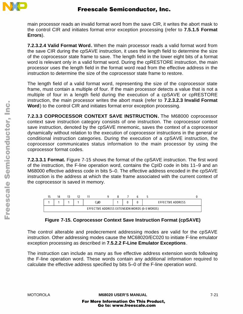
MOTOROLA M68020 USER’S MANUAL 7-21
main processor reads an invalid format word from the save CIR, it writes the abort mask tothe control CIR and initiates format error exception processing (refer to 7.5.1.5 FormatErrors).
7.2.3.2.4 Valid Format Word. When the main processor reads a valid format word fromthe save CIR during the cpSAVE instruction, it uses the length field to determine the sizeof the coprocessor state frame to save. The length field in the lower eight bits of a formatword is relevant only in a valid format word. During the cpRESTORE instruction, the mainprocessor uses the length field in the format word read from the effective address in theinstruction to determine the size of the coprocessor state frame to restore.
The length field of a valid format word, representing the size of the coprocessor stateframe, must contain a multiple of four. If the main processor detects a value that is not amultiple of four in a length field during the execution of a cpSAVE or cpRESTOREinstruction, the main processor writes the abort mask (refer to 7.2.3.2.3 Invalid FormatWord) to the control CIR and initiates format error exception processing.
7.2.3.3 COPROCESSOR CONTEXT SAVE INSTRUCTION. The M68000 coprocessorcontext save instruction category consists of one instruction. The coprocessor contextsave instruction, denoted by the cpSAVE mnemonic, saves the context of a coprocessordynamically without relation to the execution of coprocessor instructions in the general orconditional instruction categories. During the execution of a cpSAVE instruction, thecoprocessor communicates status information to the main processor by using thecoprocessor format codes.
7.2.3.3.1 Format. Figure 7-15 shows the format of the cpSAVE instruction. The first wordof the instruction, the F-line operation word, contains the CpID code in bits 11–9 and anM68000 effective address code in bits 5–0. The effective address encoded in the cpSAVEinstruction is the address at which the state frame associated with the current context ofthe coprocessor is saved in memory.
1
15
1
14
1
13
1
12 11
CpID
9
1
8
0
7
0
6 5
EFFECTIVE ADDRESS
0
EFFECTIVE ADDRESS EXTENSION WORDS (0–5 WORDS)
Figure 7-15. Coprocessor Context Save Instruction Format (cpSAVE)
The control alterable and predecrement addressing modes are valid for the cpSAVEinstruction. Other addressing modes cause the MC68020/EC020 to initiate F-line emulatorexception processing as described in 7.5.2.2 F-Line Emulator Exceptions.
The instruction can include as many as five effective address extension words followingthe F-line operation word. These words contain any additional information required tocalculate the effective address specified by bits 5–0 of the F-line operation word.
Fre
esc
ale
Se
mic
on
du
cto
r, I
Freescale Semiconductor, Inc.
For More Information On This Product, Go to: www.freescale.com
nc
...
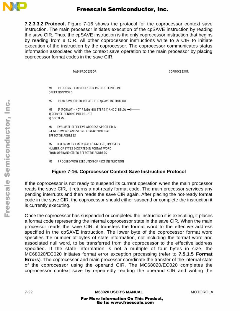
7-22 M68020 USER’S MANUAL MOTOROLA
7.2.3.3.2 Protocol. Figure 7-16 shows the protocol for the coprocessor context saveinstruction. The main processor initiates execution of the cpSAVE instruction by readingthe save CIR. Thus, the cpSAVE instruction is the only coprocessor instruction that beginsby reading from a CIR. All other coprocessor instructions write to a CIR to initiateexecution of the instruction by the coprocessor. The coprocessor communicates statusinformation associated with the context save operation to the main processor by placingcoprocessor format codes in the save CIR.
M1 RECOGNIZE COPROCESSOR INSTRUCTION F-LINEOPERATION WORD
M2 READ SAVE CIR TO INITIATE THE cpSAVE INSTRUCTION
M3 IF (FORMAT = NOT READY) DO STEPS 1) AND 2) BELOW1) SERVICE PENDING INTERRUPTS2) GO TO M2
M4 EVALUATE EFFECTIVE ADDRESS SPECIFIED IN F-LINE OPWORD AND STORE FORMAT WORD AT EFFECTIVE ADDRESS
M5 IF (FORMAT = EMPTY) GO TO M6 ELSE, TRANSFERNUMBER OF BYTES INDICATED IN FORMAT WORDFROM OPERAND CIR TO EFFECTIVE ADDRESS
M6 PROCEED WITH EXECUTION OF NEXT INSTRUCTION
MAIN PROCESSOR COPROCESSOR
Figure 7-16. Coprocessor Context Save Instruction Protocol
If the coprocessor is not ready to suspend its current operation when the main processorreads the save CIR, it returns a not-ready format code. The main processor services anypending interrupts and then reads the save CIR again. After placing the not-ready formatcode in the save CIR, the coprocessor should either suspend or complete the instruction itis currently executing.
Once the coprocessor has suspended or completed the instruction it is executing, it placesa format code representing the internal coprocessor state in the save CIR. When the mainprocessor reads the save CIR, it transfers the format word to the effective addressspecified in the cpSAVE instruction. The lower byte of the coprocessor format wordspecifies the number of bytes of state information, not including the format word andassociated null word, to be transferred from the coprocessor to the effective addressspecified. If the state information is not a multiple of four bytes in size, theMC68020/EC020 initiates format error exception processing (refer to 7.5.1.5 FormatErrors). The coprocessor and main processor coordinate the transfer of the internal stateof the coprocessor using the operand CIR. The MC68020/EC020 completes thecoprocessor context save by repeatedly reading the operand CIR and writing the
Fre
esc
ale
Se
mic
on
du
cto
r, I
Freescale Semiconductor, Inc.
For More Information On This Product, Go to: www.freescale.com
nc
...
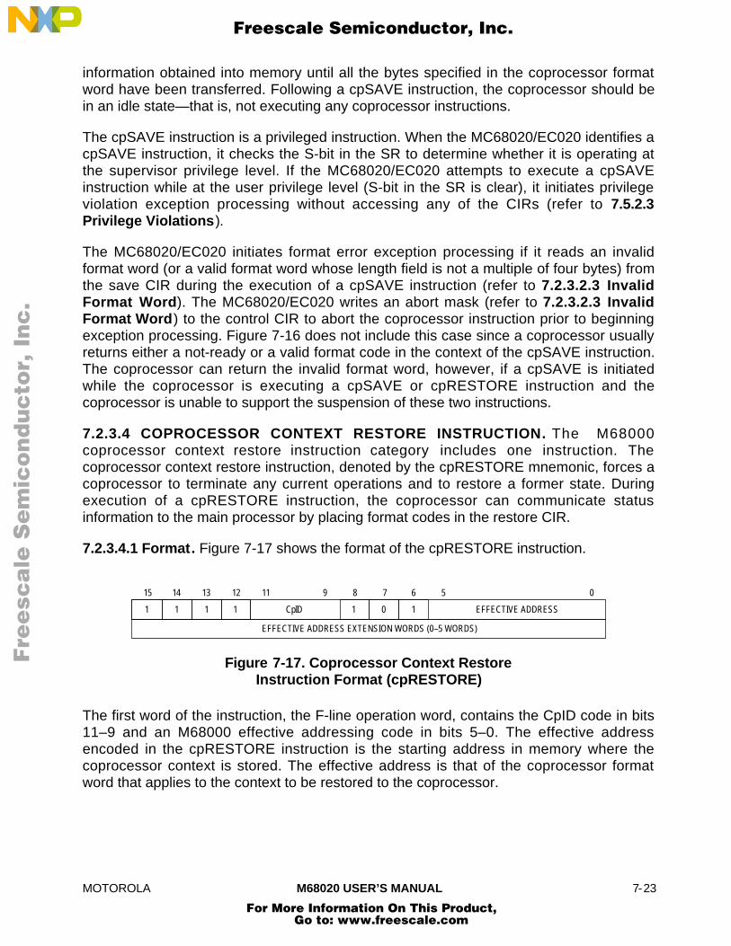
MOTOROLA M68020 USER’S MANUAL 7-23
information obtained into memory until all the bytes specified in the coprocessor formatword have been transferred. Following a cpSAVE instruction, the coprocessor should bein an idle state—that is, not executing any coprocessor instructions.
The cpSAVE instruction is a privileged instruction. When the MC68020/EC020 identifies acpSAVE instruction, it checks the S-bit in the SR to determine whether it is operating atthe supervisor privilege level. If the MC68020/EC020 attempts to execute a cpSAVEinstruction while at the user privilege level (S-bit in the SR is clear), it initiates privilegeviolation exception processing without accessing any of the CIRs (refer to 7.5.2.3Privilege Violations).
The MC68020/EC020 initiates format error exception processing if it reads an invalidformat word (or a valid format word whose length field is not a multiple of four bytes) fromthe save CIR during the execution of a cpSAVE instruction (refer to 7.2.3.2.3 InvalidFormat Word). The MC68020/EC020 writes an abort mask (refer to 7.2.3.2.3 InvalidFormat Word) to the control CIR to abort the coprocessor instruction prior to beginningexception processing. Figure 7-16 does not include this case since a coprocessor usuallyreturns either a not-ready or a valid format code in the context of the cpSAVE instruction.The coprocessor can return the invalid format word, however, if a cpSAVE is initiatedwhile the coprocessor is executing a cpSAVE or cpRESTORE instruction and thecoprocessor is unable to support the suspension of these two instructions.
7.2.3.4 COPROCESSOR CONTEXT RESTORE INSTRUCTION. The M68000coprocessor context restore instruction category includes one instruction. Thecoprocessor context restore instruction, denoted by the cpRESTORE mnemonic, forces acoprocessor to terminate any current operations and to restore a former state. Duringexecution of a cpRESTORE instruction, the coprocessor can communicate statusinformation to the main processor by placing format codes in the restore CIR.
7.2.3.4.1 Format. Figure 7-17 shows the format of the cpRESTORE instruction.
1
15
1
14
1
13
1
12 11
CpID
9
1
8
0
7
1
6 5
EFFECTIVE ADDRESS
0
EFFECTIVE ADDRESS EXTENSION WORDS (0–5 WORDS)
Figure 7-17. Coprocessor Context RestoreInstruction Format (cpRESTORE)
The first word of the instruction, the F-line operation word, contains the CpID code in bits11–9 and an M68000 effective addressing code in bits 5–0. The effective addressencoded in the cpRESTORE instruction is the starting address in memory where thecoprocessor context is stored. The effective address is that of the coprocessor formatword that applies to the context to be restored to the coprocessor.
Fre
esc
ale
Se
mic
on
du
cto
r, I
Freescale Semiconductor, Inc.
For More Information On This Product, Go to: www.freescale.com
nc
...

7-24 M68020 USER’S MANUAL MOTOROLA
The instruction can include as many as five effective address extension words followingthe F-line operation word in the cpRESTORE instruction format. These words contain anyadditional information required to calculate the effective address specified by bits 5–0 ofthe F-line operation word.
All memory addressing modes except the predecrement addressing mode are valid.Invalid effective address encodings cause the MC68020/EC020 to initiate F-line emulatorexception processing (refer to 7.5.2.2 F-Line Emulator Exceptions).
7.2.3.4.2 Protocol. Figure 7-18 shows the protocol for the coprocessor context restoreinstruction. When the main processor executes a cpRESTORE instruction, it first readsthe coprocessor format word from the effective address in the instruction. This formatword contains a format code and a length field. During cpRESTORE operation, the mainprocessor retains a copy of the length field to determine the number of bytes to betransferred to the coprocessor during the cpRESTORE operation and writes the formatword to the restore CIR to initiate the coprocessor context restore.
M1 RECOGNIZE COPROCESSOR INSTRUCTION F-LINEOPERATION WORD
M2 READ COPROCESSOR FORMAT CODE FROM EFFECTIVE ADDRESS SPECIFIED IN OPERATION WORD
M3 WRITE COPROCESSOR FORMAT WORD TORESTORE CIR
M4 READ RESTORE CIR
M5 IF (FORMAT = INVALID FORMAT) WRITE $0001 ABORTCODE TO CONTROL CIR AND INITIATE FORMAT ERROREXCEPTION PROCESSING (SEE NOTE 1)
M6 IF (FORMAT = EMPTY/RESET) GO TO M7; ELSE, TRANSFERNUMBER OF BYTES SPECIFIED BY FORMAT WORD TOOPERAND CIR (SEE NOTE 2)
M7 PROCEED WITH EXECUTION OF NEXT INSTRUCTION
C1 TERMINATE CURRENT OPERATIONS AND EVALUATEFORMAT WORD
C2 IF (INVALID FORMAT) PLACE INVALID FORMAT CODEIN THE RESTORE CIR
C3 IF (VALID FORMAT) RECEIVE NUMBER OF BYTES INDICATED IN FORMAT WORD THROUGH OPERAND CIR
MAIN PROCESSOR COPROCESSOR
NOTES: 1. See 7.6.1.5 Format Error.2. The MC68020/EC020 uses the length field in the format word read during M2 to determine the number of bytes to read from memory and write to the operand CIR.
Figure 7-18. Coprocessor Context Restore Instruction Protocol
When the coprocessor receives the format word in the restore CIR, it must terminate anycurrent operations and evaluate the format word. If the format word represents a validcoprocessor context as determined by the coprocessor design, the coprocessor returnsthe format word to the main processor through the restore CIR and prepares to receivethe number of bytes specified in the format word through its operand CIR.
Fre
esc
ale
Se
mic
on
du
cto
r, I
Freescale Semiconductor, Inc.
For More Information On This Product, Go to: www.freescale.com
nc
...
MOTOROLA M68020 USER’S MANUAL 7-25
After writing the format word to the restore CIR, the main processor continuescpRESTORE dialog by reading that same register. If the coprocessor returns a validformat word, the main processor transfers the number of bytes specified by the formatword at the effective address to the operand CIR.
If the format word written to the restore CIR does not represent a valid coprocessor stateframe, the coprocessor places an invalid format word in the restore CIR and terminatesany current operations. The main processor receives the invalid format code, writes anabort mask (refer to 7.2.3.2.3 Invalid Format Word) to the control CIR, and initiatesformat error exception processing (refer to 7.5.1.5 Format Errors).
The cpRESTORE instruction is a privileged instruction. When the MC68020/EC020accesses a cpRESTORE instruction, it checks the S-bit in the SR. If the MC68020/EC020attempts to execute a cpRESTORE instruction while at the user privilege level (S-bit in theSR is clear), it initiates privilege violation exception processing without accessing any ofthe CIRs (refer to 7.5.2.3 Privilege Violations).
7.3 COPROCESSOR INTERFACE REGISTER SET
The instructions of the M68000 coprocessor interface use registers of the CIR set tocommunicate with the coprocessor. These CIRs are not directly related to the coprocessorprogramming model.
Figure 7-4 is a memory map of the CIR set. The response, control, save, restore,command, condition, and operand registers must be included in a coprocessor interfacethat implements all four coprocessor instruction categories. The complete register modelmust be implemented if the system uses all coprocessor response primitives defined forthe M68000 coprocessor interface.
The following paragraphs contain detailed descriptions of the registers.
7.3.1 Response CIR
The coprocessor uses the 16-bit response CIR to communicate all service requests(coprocessor response primitives) to the main processor. The main processor reads theresponse CIR to receive the coprocessor response primitives during the execution ofinstructions in the general and conditional instruction categories. The offset from the baseaddress of the CIR set for the response CIR is $00. Refer to 7.4 Coprocessor ResponsePrimitives for additional information.
7.3.2 Control CIR
The main processor writes to the 2-bit control CIR to acknowledge coprocessor-requestedexception processing or to abort the execution of a coprocessor instruction. The offsetfrom the base address of the CIR set for the control CIR is $02. The control CIR occupiesthe two least significant bits of the word at that offset. The 14 most significant bits of theword are undefined and reserved by Motorola. Figure 7-19 shows the format of thisregister.
Fre
esc
ale
Se
mic
on
du
cto
r, I
Freescale Semiconductor, Inc.
For More Information On This Product, Go to: www.freescale.com
nc
...

7-26 M68020 USER’S MANUAL MOTOROLA
15
(UNDEFINED, RESERVED)
2
XA
1
AB
0
Figure 7-19. Control CIR Format
When the MC68020/EC020 receives one of the three take exception coprocessorresponse primitives, it acknowledges the primitive by setting the exception acknowledgebit (XA) in the control CIR. The MC68020/EC020 sets the abort bit (AB) in the control CIRto abort any coprocessor instruction in progress. (The 14 most significant bits of bothmasks are undefined.) The MC68020/EC020 aborts a coprocessor instruction when itdetects one of the following exception conditions:
• An F-line emulator exception condition after reading a response primitive
• A privilege violation exception as it performs a supervisor check in response to asupervisor check primitive
• A format error exception when it receives an invalid format word or a valid formatword that contains an invalid length
7.3.3 Save CIR
The coprocessor uses the 16-bit save CIR to communicate status and state frame formatinformation to the main processor while executing a cpSAVE instruction. The mainprocessor reads the save CIR to initiate execution of the cpSAVE instruction by thecoprocessor. The offset from the base address of the CIR set for the save CIR is $04.Refer to 7.2.3.2 Coprocessor Format Words for more information on the save CIR.
7.3.4 Restore CIR
The main processor initiates the cpRESTORE instruction by writing a coprocessor formatword to the 16-bit restore register. During the execution of the cpRESTORE instruction,the coprocessor communicates status and state frame format information to the mainprocessor through the restore CIR. The offset from the base address of the CIR set for therestore CIR is $06. Refer to 7.2.3.2 Coprocessor Format Words for more information onthe restore CIR.
7.3.5 Operation Word CIR
The main processor writes the F-line operation word of the instruction in progress to the16-bit operation word CIR in response to a transfer operation word coprocessor responseprimitive (refer to 7.4.6 Transfer Operation Word Primitive). The offset from the baseaddress of the CIR set for the operation word CIR is $08.
7.3.6 Command CIR
The main processor initiates a coprocessor general category instruction by writing theinstruction command word, which follows the instruction F-line operation word in theinstruction stream, to the 16-bit command CIR. The offset from the base address of theCIR set for the command CIR is $0A.
Fre
esc
ale
Se
mic
on
du
cto
r, I
Freescale Semiconductor, Inc.
For More Information On This Product, Go to: www.freescale.com
nc
...
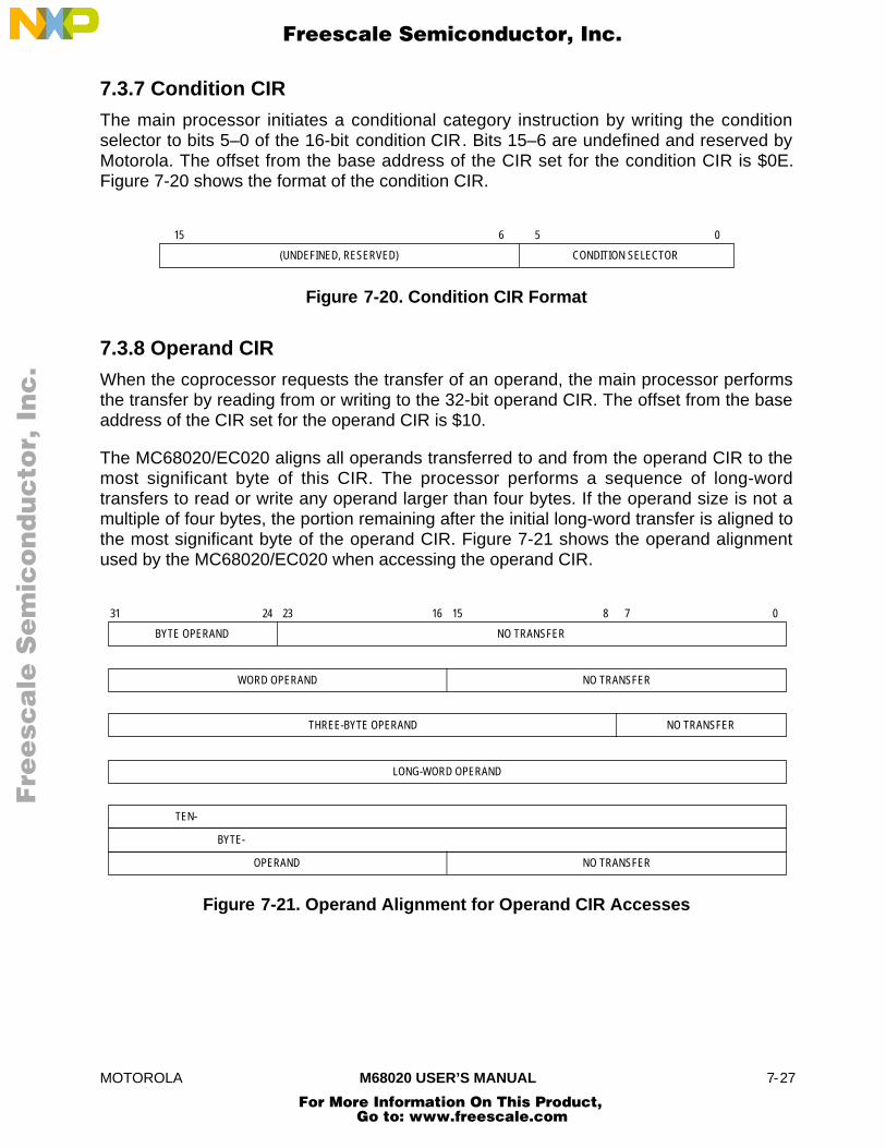
MOTOROLA M68020 USER’S MANUAL 7-27
7.3.7 Condition CIR
The main processor initiates a conditional category instruction by writing the conditionselector to bits 5–0 of the 16-bit condition CIR. Bits 15–6 are undefined and reserved byMotorola. The offset from the base address of the CIR set for the condition CIR is $0E.Figure 7-20 shows the format of the condition CIR.
15
(UNDEFINED, RESERVED)
0
CONDITION SELECTOR
56
Figure 7-20. Condition CIR Format
7.3.8 Operand CIR
When the coprocessor requests the transfer of an operand, the main processor performsthe transfer by reading from or writing to the 32-bit operand CIR. The offset from the baseaddress of the CIR set for the operand CIR is $10.
The MC68020/EC020 aligns all operands transferred to and from the operand CIR to themost significant byte of this CIR. The processor performs a sequence of long-wordtransfers to read or write any operand larger than four bytes. If the operand size is not amultiple of four bytes, the portion remaining after the initial long-word transfer is aligned tothe most significant byte of the operand CIR. Figure 7-21 shows the operand alignmentused by the MC68020/EC020 when accessing the operand CIR.
031 7
NO TRANSFER
WORD OPERAND
THREE-BYTE OPERAND
LONG-WORD OPERAND
23 15
NO TRANSFER
NO TRANSFER
NO TRANSFEROPERAND
BYTE-
TEN-
BYTE OPERAND
24 16 8
Figure 7-21. Operand Alignment for Operand CIR Accesses
Fre
esc
ale
Se
mic
on
du
cto
r, I
Freescale Semiconductor, Inc.
For More Information On This Product, Go to: www.freescale.com
nc
...

7-28 M68020 USER’S MANUAL MOTOROLA
7.3.9 Register Select CIR
When the coprocessor requests the transfer of one or more main processor registers or agroup of coprocessor registers, the main processor reads the 16-bit register select CIR toidentify the number or type of registers to be transferred. The offset from the base addressof the CIR set for the register select CIR is $14. The format of this register depends on theprimitive that is currently using it (refer to 7.4 Coprocessor Response Primitives).
7.3.10 Instruction Address CIR
When the coprocessor requests the address of the instruction it is currently executing, themain processor transfers this address to the 32-bit instruction address CIR. Any transfer ofthe scanPC is also performed through the instruction address CIR (refer to 7.4.17Transfer Status Register and ScanPC Primitive). The offset from the base address ofthe CIR set for the instruction address CIR is $18.
7.3.11 Operand Address CIR
When a coprocessor requests an operand address transfer between the main processorand the coprocessor, the address is transferred through the 32-bit operand address CIR.The offset from the base address of the CIR set for the operand address CIR is $1C.
7.4 COPROCESSOR RESPONSE PRIMITIVES
The response primitives are primitive instructions that the coprocessor issues to the mainprocessor during the execution of a coprocessor instruction. The coprocessor usesresponse primitives to communicate status information and service requests to the mainprocessor. In response to an instruction command word written to the command CIR or acondition selector in the condition CIR, the coprocessor returns a response primitive in theresponse CIR. Within the general and conditional instruction categories, individualinstructions are distinguished by the operation of the coprocessor hardware and byservices specified by coprocessor response primitives and provided by the mainprocessor.
Subsequent paragraphs, beginning with 7.4.2 Coprocessor Response PrimitiveGeneral Format, consist of detailed descriptions of the M68000 coprocessor responseprimitives supported by the MC68020/EC020. Any response primitive that theMC68020/EC020 does not recognize causes it to initiate protocol violation exceptionprocessing (refer to 7.5.2.1 Protocol Violations). This processing of undefined primitivessupports emulation of extensions to the M68000 coprocessor response primitive set bythe protocol violation exception handler. Exception processing related to the coprocessorinterface is discussed in 7.5 Exceptions.
Fre
esc
ale
Se
mic
on
du
cto
r, I
Freescale Semiconductor, Inc.
For More Information On This Product, Go to: www.freescale.com
nc
...
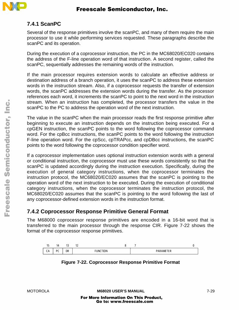
MOTOROLA M68020 USER’S MANUAL 7-29
7.4.1 ScanPC
Several of the response primitives involve the scanPC, and many of them require the mainprocessor to use it while performing services requested. These paragraphs describe thescanPC and its operation.
During the execution of a coprocessor instruction, the PC in the MC68020/EC020 containsthe address of the F-line operation word of that instruction. A second register, called thescanPC, sequentially addresses the remaining words of the instruction.
If the main processor requires extension words to calculate an effective address ordestination address of a branch operation, it uses the scanPC to address these extensionwords in the instruction stream. Also, if a coprocessor requests the transfer of extensionwords, the scanPC addresses the extension words during the transfer. As the processorreferences each word, it increments the scanPC to point to the next word in the instructionstream. When an instruction has completed, the processor transfers the value in thescanPC to the PC to address the operation word of the next instruction.
The value in the scanPC when the main processor reads the first response primitive afterbeginning to execute an instruction depends on the instruction being executed. For acpGEN instruction, the scanPC points to the word following the coprocessor commandword. For the cpBcc instructions, the scanPC points to the word following the instructionF-line operation word. For the cpScc, cpTRAPcc, and cpDBcc instructions, the scanPCpoints to the word following the coprocessor condition specifier word.
If a coprocessor implementation uses optional instruction extension words with a generalor conditional instruction, the coprocessor must use these words consistently so that thescanPC is updated accordingly during the instruction execution. Specifically, during theexecution of general category instructions, when the coprocessor terminates theinstruction protocol, the MC68020/EC020 assumes that the scanPC is pointing to theoperation word of the next instruction to be executed. During the execution of conditionalcategory instructions, when the coprocessor terminates the instruction protocol, theMC68020/EC020 assumes that the scanPC is pointing to the word following the last ofany coprocessor-defined extension words in the instruction format.
7.4.2 Coprocessor Response Primitive General Format
The M68000 coprocessor response primitives are encoded in a 16-bit word that istransferred to the main processor through the response CIR. Figure 7-22 shows theformat of the coprocessor response primitives.
15
FUNCTION
0
PARAMETERCA PC DR
14 13 12 8 7
Figure 7-22. Coprocessor Response Primitive Format
Fre
esc
ale
Se
mic
on
du
cto
r, I
Freescale Semiconductor, Inc.
For More Information On This Product, Go to: www.freescale.com
nc
...
7-30 M68020 USER’S MANUAL MOTOROLA
The encoding of bits 12–0 of a coprocessor response primitive depends on the individualprimitive. Bits 15–13, however, specify optional additional operations that apply to most ofthe primitives defined for the M68000 coprocessor interface.
The CA bit specifies the come-again operation of the main processor. When the mainprocessor reads a response primitive from the response CIR with the CA bit set, itperforms the service indicated by the primitive and then reads the response CIR again.Using the CA bit, a coprocessor can transfer several response primitives to the mainprocessor during the execution of a single coprocessor instruction.
The PC bit specifies the pass program counter operation. When the main processor readsa primitive with the PC bit set from the response CIR, the main processor immediatelypasses the current value in its program counter to the instruction address CIR as the firstoperation in servicing the primitive request. The value in the program counter is theaddress of the F-line operation word of the coprocessor instruction currently executing.The PC bit is implemented in all coprocessor response primitives currently defined for theM68000 coprocessor interface.
When an undefined primitive or a primitive that requests an illegal operation is passed tothe main processor, the main processor initiates exception processing for either an F-lineemulator or a protocol violation exception (refer to 7.5.2 Main-Processor-DetectedExceptions). If the PC bit is set in one of these response primitives, however, the mainprocessor passes the program counter to the instruction address CIR before it initiatesexception processing.
When the main processor initiates a cpGEN instruction that can be executed concurrentlywith main processor instructions, the PC bit is usually set in the first primitive returned bythe coprocessor. Since the main processor proceeds with instruction stream executiononce the coprocessor releases it, the coprocessor must record the instruction address tosupport any possible exception processing related to the instruction. Exception processingrelated to concurrent coprocessor instruction execution is discussed in 7.5.1Coprocessor-Detected Exceptions .
The DR bit is the direction bit. It applies to operand transfers between the main processorand the coprocessor. If the DR bit is clear, the direction of transfer is from the mainprocessor to the coprocessor (main processor write). If the DR bit is set, the direction oftransfer is from the coprocessor to the main processor (main processor read). If theoperation indicated by a given response primitive does not involve an explicit operandtransfer, the value of this bit depends on the particular primitive encoding.
Fre
esc
ale
Se
mic
on
du
cto
r, I
Freescale Semiconductor, Inc.
For More Information On This Product, Go to: www.freescale.com
nc
...
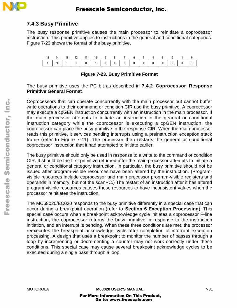
MOTOROLA M68020 USER’S MANUAL 7-31
7.4.3 Busy Primitive
The busy response primitive causes the main processor to reinitiate a coprocessorinstruction. This primitive applies to instructions in the general and conditional categories.Figure 7-23 shows the format of the busy primitive.
15 0
1 PC 1
14 13 12
0 0
11
1
10
0
9
0
8
0
7
0
6
0
5
0
4
0
3
0
2
0
1
0
Figure 7-23. Busy Primitive Format
The busy primitive uses the PC bit as described in 7.4.2 Coprocessor ResponsePrimitive General Format.
Coprocessors that can operate concurrently with the main processor but cannot bufferwrite operations to their command or condition CIR use the busy primitive. A coprocessormay execute a cpGEN instruction concurrently with an instruction in the main processor. Ifthe main processor attempts to initiate an instruction in the general or conditionalinstruction category while the coprocessor is executing a cpGEN instruction, thecoprocessor can place the busy primitive in the response CIR. When the main processorreads this primitive, it services pending interrupts using a preinstruction exception stackframe (refer to Figure 7-41). The processor then restarts the general or conditionalcoprocessor instruction that it had attempted to initiate earlier.
The busy primitive should only be used in response to a write to the command or conditionCIR. It should be the first primitive returned after the main processor attempts to initiate ageneral or conditional category instruction. In particular, the busy primitive should not beissued after program-visible resources have been altered by the instruction. (Program-visible resources include coprocessor and main processor program-visible registers andoperands in memory, but not the scanPC.) The restart of an instruction after it has alteredprogram-visible resources causes those resources to have inconsistent values when theprocessor reinitiates the instruction.
The MC68020/EC020 responds to the busy primitive differently in a special case that canoccur during a breakpoint operation (refer to Section 6 Exception Processing). Thisspecial case occurs when a breakpoint acknowledge cycle initiates a coprocessor F-lineinstruction, the coprocessor returns the busy primitive in response to the instructioninitiation, and an interrupt is pending. When these three conditions are met, the processorreexecutes the breakpoint acknowledge cycle after completion of interrupt exceptionprocessing. A design that uses a breakpoint to monitor the number of passes through aloop by incrementing or decrementing a counter may not work correctly under theseconditions. This special case may cause several breakpoint acknowledge cycles to beexecuted during a single pass through a loop.
Fre
esc
ale
Se
mic
on
du
cto
r, I
Freescale Semiconductor, Inc.
For More Information On This Product, Go to: www.freescale.com
nc
...
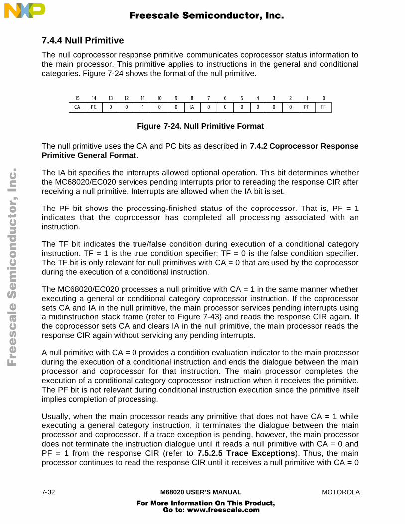
7-32 M68020 USER’S MANUAL MOTOROLA
7.4.4 Null Primitive
The null coprocessor response primitive communicates coprocessor status information tothe main processor. This primitive applies to instructions in the general and conditionalcategories. Figure 7-24 shows the format of the null primitive.
15 0
CA PC 0
14 13 12
0 1
11
0
10
0
9
IA
8
0
7
0
6
0
5
0
4
0
3
0
2
PF
1
TF
Figure 7-24. Null Primitive Format
The null primitive uses the CA and PC bits as described in 7.4.2 Coprocessor ResponsePrimitive General Format.
The IA bit specifies the interrupts allowed optional operation. This bit determines whetherthe MC68020/EC020 services pending interrupts prior to rereading the response CIR afterreceiving a null primitive. Interrupts are allowed when the IA bit is set.
The PF bit shows the processing-finished status of the coprocessor. That is, PF = 1indicates that the coprocessor has completed all processing associated with aninstruction.
The TF bit indicates the true/false condition during execution of a conditional categoryinstruction. TF = 1 is the true condition specifier; TF = 0 is the false condition specifier.The TF bit is only relevant for null primitives with CA = 0 that are used by the coprocessorduring the execution of a conditional instruction.
The MC68020/EC020 processes a null primitive with CA = 1 in the same manner whetherexecuting a general or conditional category coprocessor instruction. If the coprocessorsets CA and IA in the null primitive, the main processor services pending interrupts usinga midinstruction stack frame (refer to Figure 7-43) and reads the response CIR again. Ifthe coprocessor sets CA and clears IA in the null primitive, the main processor reads theresponse CIR again without servicing any pending interrupts.
A null primitive with CA = 0 provides a condition evaluation indicator to the main processorduring the execution of a conditional instruction and ends the dialogue between the mainprocessor and coprocessor for that instruction. The main processor completes theexecution of a conditional category coprocessor instruction when it receives the primitive.The PF bit is not relevant during conditional instruction execution since the primitive itselfimplies completion of processing.
Usually, when the main processor reads any primitive that does not have CA = 1 whileexecuting a general category instruction, it terminates the dialogue between the mainprocessor and coprocessor. If a trace exception is pending, however, the main processordoes not terminate the instruction dialogue until it reads a null primitive with CA = 0 andPF = 1 from the response CIR (refer to 7.5.2.5 Trace Exceptions). Thus, the mainprocessor continues to read the response CIR until it receives a null primitive with CA = 0
Fre
esc
ale
Se
mic
on
du
cto
r, I
Freescale Semiconductor, Inc.
For More Information On This Product, Go to: www.freescale.com
nc
...
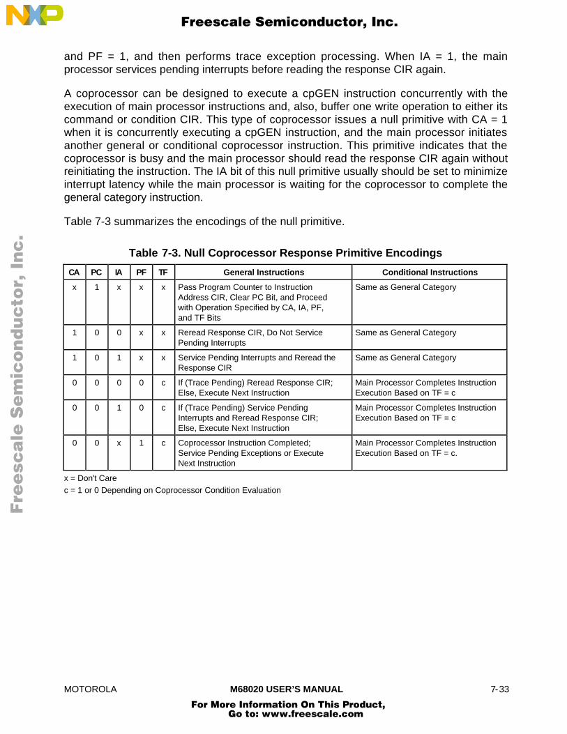
MOTOROLA M68020 USER’S MANUAL 7-33
and PF = 1, and then performs trace exception processing. When IA = 1, the mainprocessor services pending interrupts before reading the response CIR again.
A coprocessor can be designed to execute a cpGEN instruction concurrently with theexecution of main processor instructions and, also, buffer one write operation to either itscommand or condition CIR. This type of coprocessor issues a null primitive with CA = 1when it is concurrently executing a cpGEN instruction, and the main processor initiatesanother general or conditional coprocessor instruction. This primitive indicates that thecoprocessor is busy and the main processor should read the response CIR again withoutreinitiating the instruction. The IA bit of this null primitive usually should be set to minimizeinterrupt latency while the main processor is waiting for the coprocessor to complete thegeneral category instruction.
Table 7-3 summarizes the encodings of the null primitive.
Table 7-3. Null Coprocessor Response Primitive Encodings
CA PC IA PF TF General Instructions Conditional Instructions
x 1 x x x Pass Program Counter to InstructionAddress CIR, Clear PC Bit, and Proceedwith Operation Specified by CA, IA, PF,and TF Bits
Same as General Category
1 0 0 x x Reread Response CIR, Do Not ServicePending Interrupts
Same as General Category
1 0 1 x x Service Pending Interrupts and Reread theResponse CIR
Same as General Category
0 0 0 0 c If (Trace Pending) Reread Response CIR;Else, Execute Next Instruction
Main Processor Completes InstructionExecution Based on TF = c
0 0 1 0 c If (Trace Pending) Service PendingInterrupts and Reread Response CIR;Else, Execute Next Instruction
Main Processor Completes InstructionExecution Based on TF = c
0 0 x 1 c Coprocessor Instruction Completed;Service Pending Exceptions or ExecuteNext Instruction
Main Processor Completes InstructionExecution Based on TF = c.
x = Don't Carec = 1 or 0 Depending on Coprocessor Condition Evaluation
Fre
esc
ale
Se
mic
on
du
cto
r, I
Freescale Semiconductor, Inc.
For More Information On This Product, Go to: www.freescale.com
nc
...
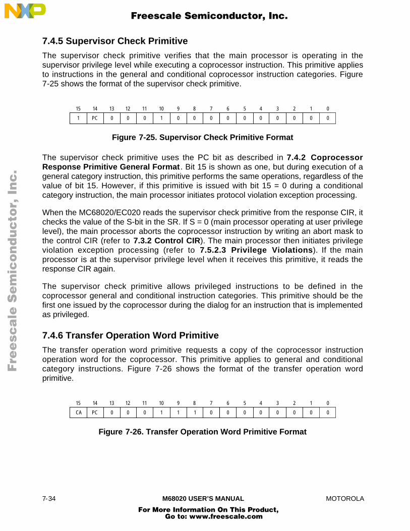
7-34 M68020 USER’S MANUAL MOTOROLA
7.4.5 Supervisor Check Primitive
The supervisor check primitive verifies that the main processor is operating in thesupervisor privilege level while executing a coprocessor instruction. This primitive appliesto instructions in the general and conditional coprocessor instruction categories. Figure7-25 shows the format of the supervisor check primitive.
15 0
1 PC 0
14 13 12
0 0
11
1
10
0
9
0
8
0
7
0
6
0
5
0
4
0
3
0
2
0
1
0
Figure 7-25. Supervisor Check Primitive Format
The supervisor check primitive uses the PC bit as described in 7.4.2 CoprocessorResponse Primitive General Format . Bit 15 is shown as one, but during execution of ageneral category instruction, this primitive performs the same operations, regardless of thevalue of bit 15. However, if this primitive is issued with bit 15 = 0 during a conditionalcategory instruction, the main processor initiates protocol violation exception processing.
When the MC68020/EC020 reads the supervisor check primitive from the response CIR, itchecks the value of the S-bit in the SR. If S = 0 (main processor operating at user privilegelevel), the main processor aborts the coprocessor instruction by writing an abort mask tothe control CIR (refer to 7.3.2 Control CIR). The main processor then initiates privilegeviolation exception processing (refer to 7.5.2.3 Privilege Violations). If the mainprocessor is at the supervisor privilege level when it receives this primitive, it reads theresponse CIR again.
The supervisor check primitive allows privileged instructions to be defined in thecoprocessor general and conditional instruction categories. This primitive should be thefirst one issued by the coprocessor during the dialog for an instruction that is implementedas privileged.
7.4.6 Transfer Operation Word Primitive
The transfer operation word primitive requests a copy of the coprocessor instructionoperation word for the coprocessor. This primitive applies to general and conditionalcategory instructions. Figure 7-26 shows the format of the transfer operation wordprimitive.
15 0
CA PC 0
14 13 12
0 0
11
1
10
1
9
1
8
0
7
0
6
0
5
0
4
0
3
0
2
0
1
0
Figure 7-26. Transfer Operation Word Primitive Format
Fre
esc
ale
Se
mic
on
du
cto
r, I
Freescale Semiconductor, Inc.
For More Information On This Product, Go to: www.freescale.com
nc
...
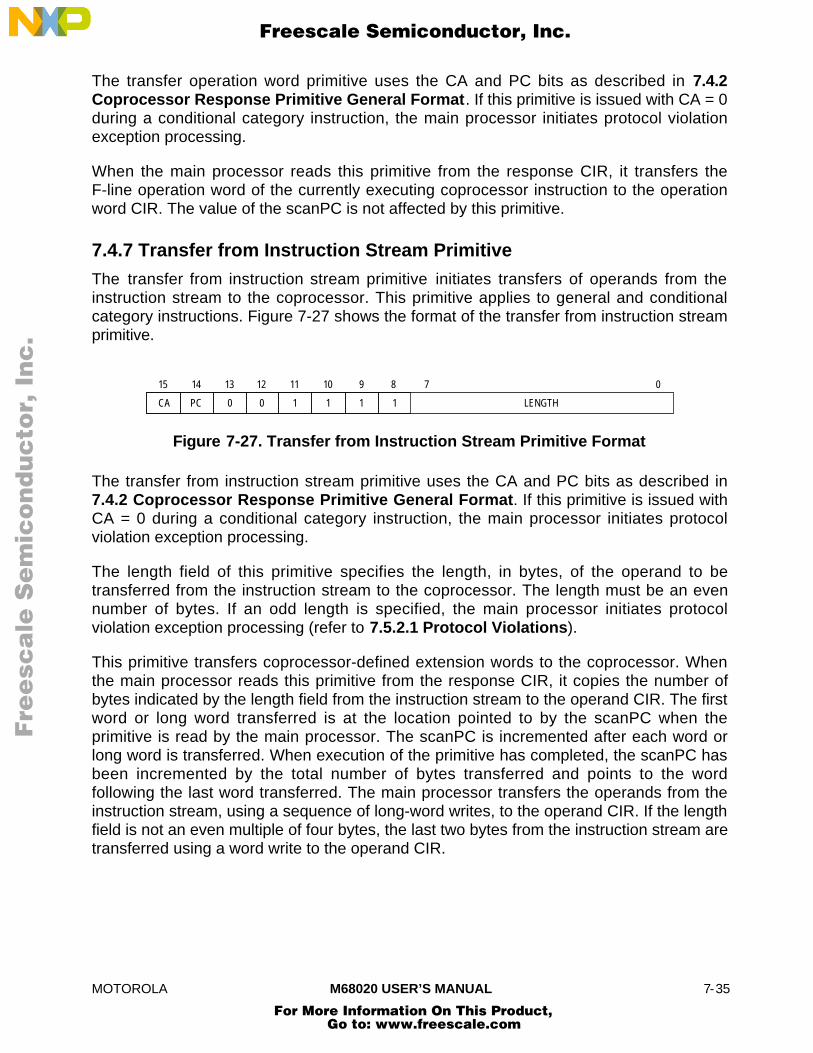
MOTOROLA M68020 USER’S MANUAL 7-35
The transfer operation word primitive uses the CA and PC bits as described in 7.4.2Coprocessor Response Primitive General Format. If this primitive is issued with CA = 0during a conditional category instruction, the main processor initiates protocol violationexception processing.
When the main processor reads this primitive from the response CIR, it transfers theF-line operation word of the currently executing coprocessor instruction to the operationword CIR. The value of the scanPC is not affected by this primitive.
7.4.7 Transfer from Instruction Stream Primitive
The transfer from instruction stream primitive initiates transfers of operands from theinstruction stream to the coprocessor. This primitive applies to general and conditionalcategory instructions. Figure 7-27 shows the format of the transfer from instruction streamprimitive.
15 0
CA PC 0
14 13 12
0 1
11
1
10
1
9
1
8 7
LENGTH
Figure 7-27. Transfer from Instruction Stream Primitive Format
The transfer from instruction stream primitive uses the CA and PC bits as described in7.4.2 Coprocessor Response Primitive General Format. If this primitive is issued withCA = 0 during a conditional category instruction, the main processor initiates protocolviolation exception processing.
The length field of this primitive specifies the length, in bytes, of the operand to betransferred from the instruction stream to the coprocessor. The length must be an evennumber of bytes. If an odd length is specified, the main processor initiates protocolviolation exception processing (refer to 7.5.2.1 Protocol Violations).
This primitive transfers coprocessor-defined extension words to the coprocessor. Whenthe main processor reads this primitive from the response CIR, it copies the number ofbytes indicated by the length field from the instruction stream to the operand CIR. The firstword or long word transferred is at the location pointed to by the scanPC when theprimitive is read by the main processor. The scanPC is incremented after each word orlong word is transferred. When execution of the primitive has completed, the scanPC hasbeen incremented by the total number of bytes transferred and points to the wordfollowing the last word transferred. The main processor transfers the operands from theinstruction stream, using a sequence of long-word writes, to the operand CIR. If the lengthfield is not an even multiple of four bytes, the last two bytes from the instruction stream aretransferred using a word write to the operand CIR.
Fre
esc
ale
Se
mic
on
du
cto
r, I
Freescale Semiconductor, Inc.
For More Information On This Product, Go to: www.freescale.com
nc
...
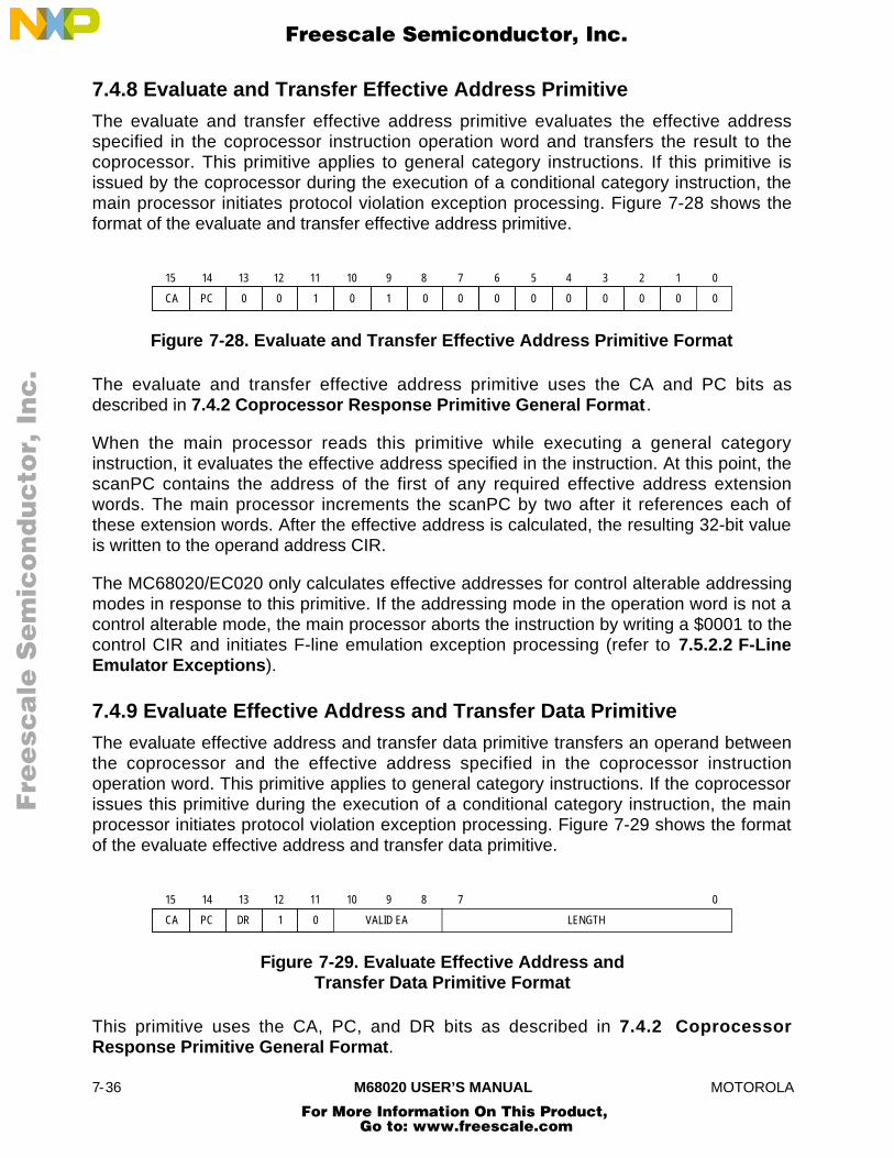
7-36 M68020 USER’S MANUAL MOTOROLA
7.4.8 Evaluate and Transfer Effective Address Primitive
The evaluate and transfer effective address primitive evaluates the effective addressspecified in the coprocessor instruction operation word and transfers the result to thecoprocessor. This primitive applies to general category instructions. If this primitive isissued by the coprocessor during the execution of a conditional category instruction, themain processor initiates protocol violation exception processing. Figure 7-28 shows theformat of the evaluate and transfer effective address primitive.
15 0
CA PC 0
14 13 12
0 1
11
0
10
1
9
0
8
0
7
0
6
0
5
0
4
0
3
0
2
0
1
0
Figure 7-28. Evaluate and Transfer Effective Address Primitive Format
The evaluate and transfer effective address primitive uses the CA and PC bits asdescribed in 7.4.2 Coprocessor Response Primitive General Format.
When the main processor reads this primitive while executing a general categoryinstruction, it evaluates the effective address specified in the instruction. At this point, thescanPC contains the address of the first of any required effective address extensionwords. The main processor increments the scanPC by two after it references each ofthese extension words. After the effective address is calculated, the resulting 32-bit valueis written to the operand address CIR.
The MC68020/EC020 only calculates effective addresses for control alterable addressingmodes in response to this primitive. If the addressing mode in the operation word is not acontrol alterable mode, the main processor aborts the instruction by writing a $0001 to thecontrol CIR and initiates F-line emulation exception processing (refer to 7.5.2.2 F-LineEmulator Exceptions).
7.4.9 Evaluate Effective Address and Transfer Data Primitive
The evaluate effective address and transfer data primitive transfers an operand betweenthe coprocessor and the effective address specified in the coprocessor instructionoperation word. This primitive applies to general category instructions. If the coprocessorissues this primitive during the execution of a conditional category instruction, the mainprocessor initiates protocol violation exception processing. Figure 7-29 shows the formatof the evaluate effective address and transfer data primitive.
15 0
CA PC DR
14 13 12
1 0
11 10 9
VALID EA
8 7
LENGTH
Figure 7-29. Evaluate Effective Address andTransfer Data Primitive Format
This primitive uses the CA, PC, and DR bits as described in 7.4.2 CoprocessorResponse Primitive General Format.
Fre
esc
ale
Se
mic
on
du
cto
r, I
Freescale Semiconductor, Inc.
For More Information On This Product, Go to: www.freescale.com
nc
...
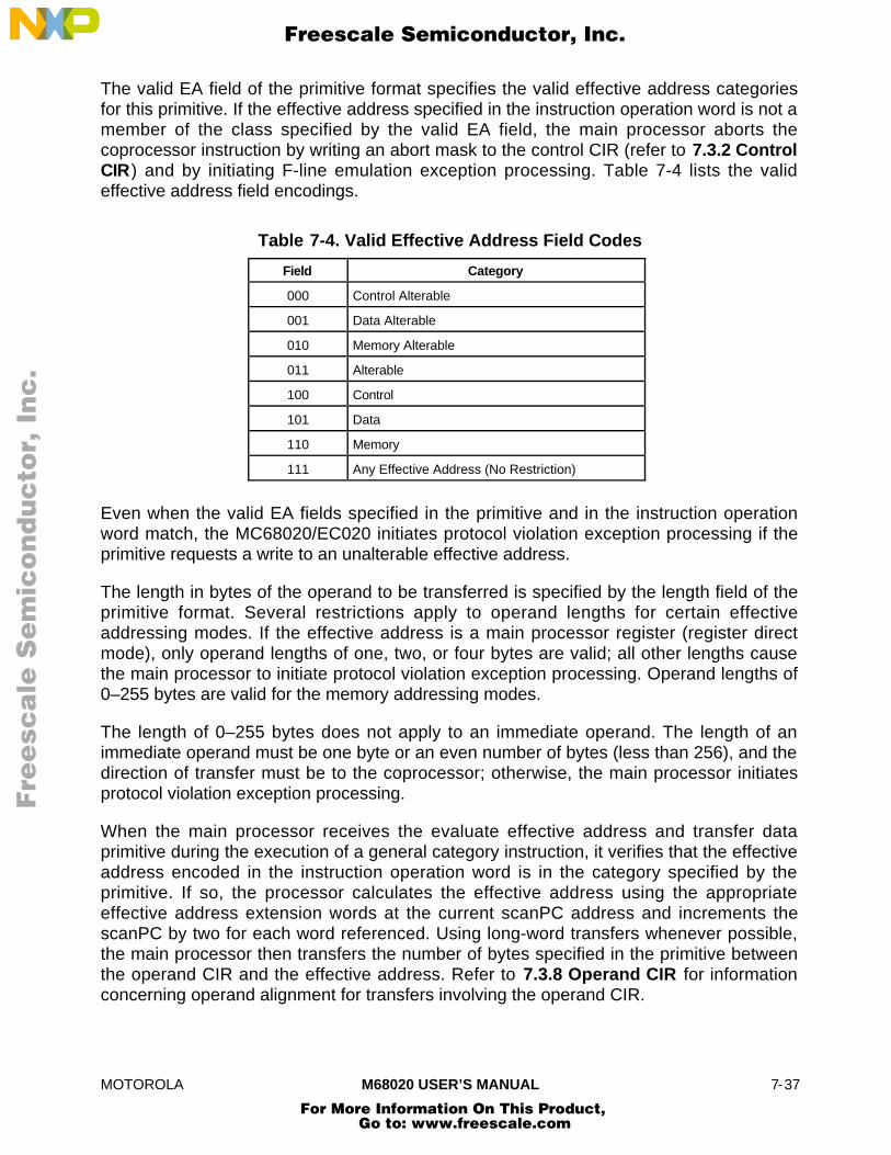
MOTOROLA M68020 USER’S MANUAL 7-37
The valid EA field of the primitive format specifies the valid effective address categoriesfor this primitive. If the effective address specified in the instruction operation word is not amember of the class specified by the valid EA field, the main processor aborts thecoprocessor instruction by writing an abort mask to the control CIR (refer to 7.3.2 ControlCIR) and by initiating F-line emulation exception processing. Table 7-4 lists the valideffective address field encodings.
Table 7-4. Valid Effective Address Field Codes
Field Category
000 Control Alterable
001 Data Alterable
010 Memory Alterable
011 Alterable
100 Control
101 Data
110 Memory
111 Any Effective Address (No Restriction)
Even when the valid EA fields specified in the primitive and in the instruction operationword match, the MC68020/EC020 initiates protocol violation exception processing if theprimitive requests a write to an unalterable effective address.
The length in bytes of the operand to be transferred is specified by the length field of theprimitive format. Several restrictions apply to operand lengths for certain effectiveaddressing modes. If the effective address is a main processor register (register directmode), only operand lengths of one, two, or four bytes are valid; all other lengths causethe main processor to initiate protocol violation exception processing. Operand lengths of0–255 bytes are valid for the memory addressing modes.
The length of 0–255 bytes does not apply to an immediate operand. The length of animmediate operand must be one byte or an even number of bytes (less than 256), and thedirection of transfer must be to the coprocessor; otherwise, the main processor initiatesprotocol violation exception processing.
When the main processor receives the evaluate effective address and transfer dataprimitive during the execution of a general category instruction, it verifies that the effectiveaddress encoded in the instruction operation word is in the category specified by theprimitive. If so, the processor calculates the effective address using the appropriateeffective address extension words at the current scanPC address and increments thescanPC by two for each word referenced. Using long-word transfers whenever possible,the main processor then transfers the number of bytes specified in the primitive betweenthe operand CIR and the effective address. Refer to 7.3.8 Operand CIR for informationconcerning operand alignment for transfers involving the operand CIR.
Fre
esc
ale
Se
mic
on
du
cto
r, I
Freescale Semiconductor, Inc.
For More Information On This Product, Go to: www.freescale.com
nc
...

7-38 M68020 USER’S MANUAL MOTOROLA
The DR bit specifies the direction of the operand transfer. DR = 0 requests a transfer fromthe main processor to the coprocessor, and DR = 1 specifies a transfer from thecoprocessor to the main processor.
If the effective addressing mode specifies the predecrement mode, the address registerused is decremented by the size of the operand before the transfer. The bytes within theoperand are then transferred to or from ascending addresses beginning with the locationspecified by the decremented address register. In this mode, if A7 is used as the addressregister and the operand length is one byte, A7 is decremented by two to maintain a word-aligned stack.
For the postincrement effective addressing mode, the address register used isincremented by the size of the operand after the transfer. The bytes within the operandare transferred to or from ascending addresses beginning with the location specified bythe address register. In this mode, if A7 is used as the address register and the operandlength is one byte, A7 is incremented by two after the transfer to maintain a word-alignedstack. Transferring odd length operands longer than one byte using the –(A7) or (A7)+addressing modes can result in a stack pointer that is not word aligned.
The processor repeats the effective address calculation each time this primitive is issuedduring the execution of a given instruction. The calculation uses the current contents ofany required address and data registers. The instruction must include a set of effectiveaddress extension words for each repetition of a calculation that requires them. Theprocessor locates these words at the current scanPC location and increments the scanPCby two for each word referenced in the instruction stream.
The MC68020/EC020 sign-extends a byte or word-sized operand to a long-word valuewhen it is transferred to an address register (A7–A0) using this primitive with the registerdirect effective addressing mode. A byte or word-sized operand transferred to a dataregister (D7–D0) only overwrites the lower byte or word of the data register.
7.4.10 Write to Previously Evaluated Effective Address Primitive
The write to previously evaluated effective address primitive transfers an operand from thecoprocessor to a previously evaluated effective address. This primitive applies to generalcategory instructions. If the coprocessor uses this primitive during the execution of aconditional category instruction, the main processor initiates protocol violation exceptionprocessing. Figure 7-30 shows the format of the write to previously evaluated effectiveaddress primitive.
15 0
CA PC 1
14 13 12
0 0
11 10 9 8 7
LENGTH0 0 0
Figure 7-30. Write to Previously Evaluated Effective Address Primitive Format
Fre
esc
ale
Se
mic
on
du
cto
r, I
Freescale Semiconductor, Inc.
For More Information On This Product, Go to: www.freescale.com
nc
...

MOTOROLA M68020 USER’S MANUAL 7-39
The write to previously evaluated effective address primitive uses the CA and PC bits asdescribed in 7.4.2 Coprocessor Response Primitive General Format.
The length field of the primitive format specifies the length of the operand in bytes. TheMC68020/EC020 transfers operands of 0–255 bytes in length.
When the main processor receives this primitive during the execution of a generalcategory instruction, it transfers an operand from the operand CIR to an effective addressspecified by a temporary register within the MC68020/EC020. When a previous primitivefor the current instruction has evaluated the effective address, this temporary registercontains the evaluated effective address. Primitives that store an evaluated effectiveaddress in a temporary register of the main processor are the evaluate and transfereffective address, evaluate effective address and transfer data, and transfer multiplecoprocessor registers primitive. If this primitive is used during an instruction in which theeffective address specified in the instruction operation word has not been calculated, theeffective address used for the write is undefined. Also, if the previously evaluated effectiveaddress was register direct, the address written to in response to this primitive isundefined.
The function code value during the write operation indicates either supervisor or user dataspace, depending on the value of the S-bit in the MC68020/EC020 SR when theprocessor reads this primitive. While a coprocessor should request writes to only alterableeffective addressing modes, the MC68020/EC020 does not check the type of effectiveaddress used with this primitive. For example, if the previously evaluated effective addresswas PC relative and the MC68020/EC020 is at the user privilege level (S = 0 in SR), theMC68020/EC020 writes to user data space at the previously calculated program relativeaddress (the 32-bit value in the temporary internal register of the processor).
Operands longer than four bytes are transferred in increments of four bytes (operandparts) when possible. The main processor reads a long-word operand part from theoperand CIR and transfers this part to the current effective address. The transferscontinue in this manner using ascending memory locations until all of the long-wordoperand parts are transferred, and any remaining operand part is then transferred using aone-, two-, or three-byte transfer as required. The operand parts are stored in memoryusing ascending addresses beginning with the address in the MC68020/EC020 temporaryregister, which is internal to the processor and not for user use.
The execution of this primitive does not modify any of the registers in theMC68020/EC020 programming model, even if the previously evaluated effective addressmode is the predecrement or postincrement mode. If the previously evaluated effectiveaddressing mode used any of the MC68020/EC020 internal address or data registers, theeffective address value used is the final value from the preceding primitive. That is, thisprimitive uses the value from an evaluate and transfer effective address, evaluate effectiveaddress and transfer data, or transfer multiple coprocessor registers primitive withoutmodification.
Fre
esc
ale
Se
mic
on
du
cto
r, I
Freescale Semiconductor, Inc.
For More Information On This Product, Go to: www.freescale.com
nc
...

7-40 M68020 USER’S MANUAL MOTOROLA
The take address and transfer data primitive described in 7.4.11 Take Address andTransfer Data Primitive does not replace the effective address value that has beencalculated by the MC68020/EC020. The address that the main processor obtains inresponse to the take address and transfer data primitive is not available to the write topreviously evaluated effective address primitive.
A coprocessor can issue an evaluate effective address and transfer data primitive followedby this primitive to perform a read-modify-write operation that is not indivisible. The buscycles for this operation are normal bus cycles that can be interrupted, and the bus can bearbitrated between the cycles.
7.4.11 Take Address and Transfer Data Primitive
The take address and transfer data primitive transfers an operand between thecoprocessor and an address supplied by the coprocessor. This primitive applies to generaland conditional category instructions. Figure 7-31 shows the format of the take addressand transfer data primitive.
15 0
CA PC DR
14 13 12
0 0
11 10 9 8 7
LENGTH1 0 1
Figure 7-31. Take Address and Transfer Data Primitive Format
The take address and transfer data primitive uses the CA, PC, and DR bits as describedin 7.4.2 Coprocessor Response Primitive General Format. If the coprocessor issuesthis primitive with CA = 0 during a conditional category instruction, the main processorinitiates protocol violation exception processing.
The length field of the primitive format specifies the operand length, which can be from0–255 bytes.
The main processor reads a 32-bit address from the operand address CIR. Using a seriesof long-word transfers, the processor transfers the operand between this address and theoperand CIR. The DR bit determines the direction of the transfer. The processor reads orwrites the operand parts to ascending addresses, starting at the address from the operandaddress CIR. If the operand length is not a multiple of four bytes, the final operand part istransferred using a one-, two-, or three-byte transfer as required.
The function code used with the address read from the operand address CIR indicateseither supervisor or user data space according to the value of the S-bit in theMC68020/EC020 SR.
Fre
esc
ale
Se
mic
on
du
cto
r, I
Freescale Semiconductor, Inc.
For More Information On This Product, Go to: www.freescale.com
nc
...

MOTOROLA M68020 USER’S MANUAL 7-41
7.4.12 Transfer to/from Top of Stack Primitive
The transfer to/from top of stack primitive transfers an operand between the coprocessorand the top of the active system stack of the main processor. This primitive applies togeneral and conditional category instructions. Figure 7-32 shows the format of the transferto/from top of stack primitive.
15 0
CA PC DR
14 13 12
0 1
11 10 9 8 7
LENGTH1 1 0
Figure 7-32. Transfer to/from Top of Stack Primitive Format
The transfer to/from top of stack primitive uses the CA, PC, and DR bits as described in7.4.2 Coprocessor Response Primitive General Format. If the coprocessor issues thisprimitive with CA = 0 during a conditional category instruction, the main processor initiatesprotocol violation exception processing.
The length field of the primitive format specifies the length in bytes of the operand to betransferred. The operand may be one, two, or four bytes in length; other length valuescause the main processor to initiate protocol violation exception processing.
If DR = 0, the main processor transfers the operand from the active system stack to theoperand CIR. The implied effective address mode used for the transfer is the (A7)+addressing mode. A one-byte operand causes the stack pointer to be incremented by twoafter the transfer to maintain word alignment of the stack.
If DR = 1, the main processor transfers the operand from the operand CIR to the activesystem stack. The implied effective address mode used for the transfer is the –(A7)addressing mode. A one-byte operand causes the stack pointer to be decremented by twobefore the transfer to maintain word alignment of the stack.
7.4.13 Transfer Single Main Processor Register Primitive
The transfer single main processor register primitive transfers an operand between one ofthe main processor's data or address registers and the coprocessor. This primitive appliesto general and conditional category instructions. Figure 7-33 shows the format of thetransfer single main processor register primitive.
15
CA PC DR
14 13 12
0 1
11 10 9 07
1 0
2
REGISTER
3
D/A
4
0
5
0
6
000
8
Figure 7-33. Transfer Single Main Processor Register Primitive Format
The transfer single main processor register primitive uses the CA, PC, and DR bits asdescribed in 7.4.2 Coprocessor Response Primitive General Format. If thecoprocessor issues this primitive with CA = 0 during a conditional category instruction, themain processor initiates protocol violation exception processing.
Fre
esc
ale
Se
mic
on
du
cto
r, I
Freescale Semiconductor, Inc.
For More Information On This Product, Go to: www.freescale.com
nc
...
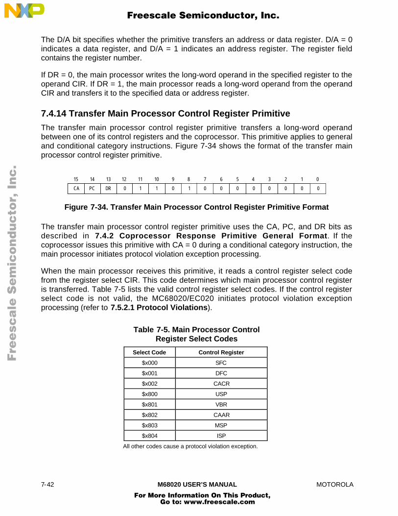
7-42 M68020 USER’S MANUAL MOTOROLA
The D/A bit specifies whether the primitive transfers an address or data register. D/A = 0indicates a data register, and D/A = 1 indicates an address register. The register fieldcontains the register number.
If DR = 0, the main processor writes the long-word operand in the specified register to theoperand CIR. If DR = 1, the main processor reads a long-word operand from the operandCIR and transfers it to the specified data or address register.
7.4.14 Transfer Main Processor Control Register Primitive
The transfer main processor control register primitive transfers a long-word operandbetween one of its control registers and the coprocessor. This primitive applies to generaland conditional category instructions. Figure 7-34 shows the format of the transfer mainprocessor control register primitive.
15
CA PC DR
14 13 12
0 1
11 10 9 07
1 0
2
0
3
0
4
0
5
0
6
001
8
0 0
1
Figure 7-34. Transfer Main Processor Control Register Primitive Format
The transfer main processor control register primitive uses the CA, PC, and DR bits asdescribed in 7.4.2 Coprocessor Response Primitive General Format. If thecoprocessor issues this primitive with CA = 0 during a conditional category instruction, themain processor initiates protocol violation exception processing.
When the main processor receives this primitive, it reads a control register select codefrom the register select CIR. This code determines which main processor control registeris transferred. Table 7-5 lists the valid control register select codes. If the control registerselect code is not valid, the MC68020/EC020 initiates protocol violation exceptionprocessing (refer to 7.5.2.1 Protocol Violations).
Table 7-5. Main Processor ControlRegister Select Codes
Select Code Control Register
$x000 SFC
$x001 DFC
$x002 CACR
$x800 USP
$x801 VBR
$x802 CAAR
$x803 MSP
$x804 ISP
All other codes cause a protocol violation exception.
Fre
esc
ale
Se
mic
on
du
cto
r, I
Freescale Semiconductor, Inc.
For More Information On This Product, Go to: www.freescale.com
nc
...
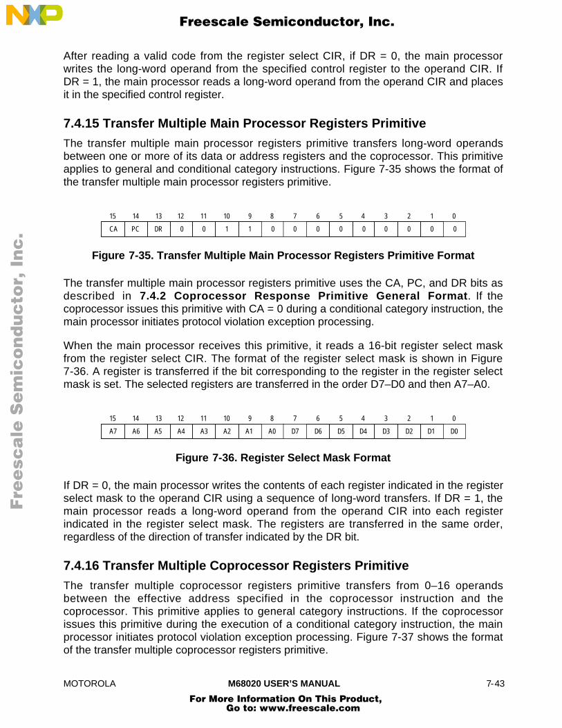
MOTOROLA M68020 USER’S MANUAL 7-43
After reading a valid code from the register select CIR, if DR = 0, the main processorwrites the long-word operand from the specified control register to the operand CIR. IfDR = 1, the main processor reads a long-word operand from the operand CIR and placesit in the specified control register.
7.4.15 Transfer Multiple Main Processor Registers Primitive
The transfer multiple main processor registers primitive transfers long-word operandsbetween one or more of its data or address registers and the coprocessor. This primitiveapplies to general and conditional category instructions. Figure 7-35 shows the format ofthe transfer multiple main processor registers primitive.
15
CA PC DR
14 13 12
0 0
11 10 9 07
1 1
2
0
3
0
4
0
5
0
6
000
8
0 0
1
Figure 7-35. Transfer Multiple Main Processor Registers Primitive Format
The transfer multiple main processor registers primitive uses the CA, PC, and DR bits asdescribed in 7.4.2 Coprocessor Response Primitive General Format. If thecoprocessor issues this primitive with CA = 0 during a conditional category instruction, themain processor initiates protocol violation exception processing.
When the main processor receives this primitive, it reads a 16-bit register select maskfrom the register select CIR. The format of the register select mask is shown in Figure7-36. A register is transferred if the bit corresponding to the register in the register selectmask is set. The selected registers are transferred in the order D7–D0 and then A7–A0.
15
A7 A6 A5
14 13 12
A4 A3
11 10 9 07
A2 A1
2
D1
3
D3
4
D4
5
D5
6
D6D7A0
8
D2 D0
1
Figure 7-36. Register Select Mask Format
If DR = 0, the main processor writes the contents of each register indicated in the registerselect mask to the operand CIR using a sequence of long-word transfers. If DR = 1, themain processor reads a long-word operand from the operand CIR into each registerindicated in the register select mask. The registers are transferred in the same order,regardless of the direction of transfer indicated by the DR bit.
7.4.16 Transfer Multiple Coprocessor Registers Primitive
The transfer multiple coprocessor registers primitive transfers from 0–16 operandsbetween the effective address specified in the coprocessor instruction and thecoprocessor. This primitive applies to general category instructions. If the coprocessorissues this primitive during the execution of a conditional category instruction, the mainprocessor initiates protocol violation exception processing. Figure 7-37 shows the formatof the transfer multiple coprocessor registers primitive.
Fre
esc
ale
Se
mic
on
du
cto
r, I
Freescale Semiconductor, Inc.
For More Information On This Product, Go to: www.freescale.com
nc
...

7-44 M68020 USER’S MANUAL MOTOROLA
15 0
CA PC DR
14 13 12
0 0
11 10 9 8 7
LENGTH0 0 1
Figure 7-37. Transfer Multiple Coprocessor Registers Primitive Format
The transfer multiple coprocessor registers primitive uses the CA, PC, and DR bits asdescribed in 7.4.2 Coprocessor Response Primitive General Format.
The length field of the primitive format indicates the length in bytes of each operandtransferred. The operand length must be an even number of bytes; odd length operandscause the MC68020/EC020 to initiate protocol violation exception processing (refer to7.5.2.1 Protocol Violations).
When the main processor reads this primitive, it calculates the effective address specifiedin the coprocessor instruction. The scanPC should be pointing to the first of any necessaryeffective address extension words when this primitive is read from the response CIR; thescanPC is incremented by two for each extension word referenced during the effectiveaddress calculation. For transfers from the effective address to the coprocessor (DR = 0),the control addressing modes and the postincrement addressing mode are valid. Fortransfers from the coprocessor to the effective address (DR = 1), the control alterable andpredecrement addressing modes are valid. Invalid addressing modes cause theMC68020/EC020 to abort the instruction by writing an abort mask to the control CIR (referto 7.3.2 Control CIR) and to initiate F-line emulator exception processing (refer to 7.5.2.2F-Line Emulator Exceptions).
After performing the effective address calculation, the MC68020/EC020 reads a 16-bitregister select mask from the register select CIR. The coprocessor uses the register selectmask to specify the number of operands to transfer; the MC68020/EC020 counts thenumber of ones in the register select mask to determine the number of operands. Theorder of the ones in the register select mask is not relevant to the operation of the mainprocessor. As many as 16 operands can be transferred by the main processor in responseto this primitive. The total number of bytes transferred is the product of the number ofoperands transferred and the length of each operand specified in the length field of theprimitive format.
If DR = 1, the main processor reads the number of operands specified in the registerselect mask from the operand CIR and writes these operands to the effective addressspecified in the instruction using long-word transfers whenever possible. If DR = 0, themain processor reads the number of operands specified in the register select mask fromthe effective address and writes them to the operand CIR.
For the control addressing modes, the operands are transferred to or from memory usingascending addresses. For the postincrement addressing mode, the operands are readfrom memory with ascending addresses also, and the address register used isincremented by the size of an operand after each operand is transferred. The addressregister used with the (An)+ addressing mode is incremented by the total number of bytestransferred during the primitive execution.
Fre
esc
ale
Se
mic
on
du
cto
r, I
Freescale Semiconductor, Inc.
For More Information On This Product, Go to: www.freescale.com
nc
...
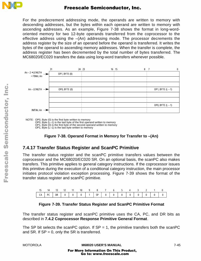
MOTOROLA M68020 USER’S MANUAL 7-45
For the predecrement addressing mode, the operands are written to memory withdescending addresses, but the bytes within each operand are written to memory withascending addresses. As an example, Figure 7-38 shows the format in long-word-oriented memory for two 12-byte operands transferred from the coprocessor to theeffective address using the –(An) addressing mode. The processor decrements theaddress register by the size of an operand before the operand is transferred. It writes thebytes of the operand to ascending memory addresses. When the transfer is complete, theaddress register has been decremented by the total number of bytes transferred. TheMC68020/EC020 transfers the data using long-word transfers whenever possible.
31 15 0
OP1, BYTE (0)
723
OP0, BYTE (0) OP1, BYTE (L – 1)
OP0, BYTE (L – 1)
An – LENGTH
INITIAL An
OP0, Byte (0) is the first byte written to memoryOP0, Byte (L–1) is the last byte of the first operand written to memoryOP1, Byte (0) is the first byte of the second operand written to memoryOP1, Byte (L–1) is the last byte written to memory
NOTE:
16 824An – 2 LENGTH
= FINAL An*
Figure 7-38. Operand Format in Memory for Transfer to –(An)
7.4.17 Transfer Status Register and ScanPC Primitive
The transfer status register and the scanPC primitive transfers values between thecoprocessor and the MC68020/EC020 SR. On an optional basis, the scanPC also makestransfers. This primitive applies to general category instructions. If the coprocessor issuesthis primitive during the execution of a conditional category instruction, the main processorinitiates protocol violation exception processing. Figure 7-39 shows the format of thetransfer status register and scanPC primitive.
15
CA PC DR
14 13 12
0 0
11 10 9 07
0 1
2
0
3
0
4
0
5
0
6
00SP
8
0 0
1
Figure 7-39. Transfer Status Register and ScanPC Primitive Format
The transfer status register and scanPC primitive uses the CA, PC, and DR bits asdescribed in 7.4.2 Coprocessor Response Primitive General Format.
The SP bit selects the scanPC option. If SP = 1, the primitive transfers both the scanPCand SR. If SP = 0, only the SR is transferred.
Fre
esc
ale
Se
mic
on
du
cto
r, I
Freescale Semiconductor, Inc.
For More Information On This Product, Go to: www.freescale.com
nc
...

7-46 M68020 USER’S MANUAL MOTOROLA
If SP = 0 and DR = 0, the main processor writes the 16-bit SR value to the operand CIR. IfSP = 0 and DR = 1, the main processor reads a 16-bit value from the operand CIR into themain processor SR.
If SP = 1 and DR = 0, the main processor writes the long-word value in the scanPC to theinstruction address CIR and then writes the SR value to the operand CIR. If SP = 1 andDR = 1, the main processor reads a 16-bit value from the operand CIR into the SR andthen reads a long-word value from the instruction address CIR into the scanPC.
With this primitive, a general category instruction can change the main processor programflow by placing a new value in the SR, in the scanPC, or new values in both the SR andthe scanPC. By accessing the SR, the coprocessor can determine and manipulate themain processor condition codes, supervisor status, trace modes, selection of the activestack, and interrupt mask level.
The MC68020/EC020 discards any instruction words that have been prefetched beyondthe current scanPC location when this primitive is issued with DR = 1 (transfer to mainprocessor). The MC68020/EC020 then refills the instruction pipe from the scanPCaddress in the address space indicated by the S-bit of the SR.
If the MC68020/EC020 is operating in the trace on change of flow mode (T1, T0 in the SR= 01) when the coprocessor instruction begins to execute and if this primitive is issuedwith DR = 1 (from coprocessor to main processor), the MC68020/EC020 prepares to takea trace exception. The trace exception occurs when the coprocessor signals that it hascompleted all processing associated with the instruction. Changes in the trace modes dueto the transfer of the SR to the main processor take effect on execution of the nextinstruction.
7.4.18 Take Preinstruction Exception Primitive
The take preinstruction exception primitive initiates exception processing using acoprocessor-supplied exception vector number and the preinstruction exception stackframe format. This primitive applies to general and conditional category instructions.Figure 7-40 shows the format of the take preinstruction exception primitive.
15 0
0 PC 0
14 13 12
1 1
11 10 9 8 7
VECTOR NUMBER1 0 0
Figure 7-40. Take Preinstruction Exception Primitive Format
The take preinstruction exception primitive uses the PC bit as described in 7.4.2Coprocessor Response Primitive General Format. The vector number field containsthe exception vector number used by the main processor to initiate exception processing.
When the main processor receives this primitive, it acknowledges the coprocessorexception request by writing an exception acknowledge mask to the control CIR (refer to7.3.2 Control CIR). The MC68020/EC020 then proceeds with exception processing as
Fre
esc
ale
Se
mic
on
du
cto
r, I
Freescale Semiconductor, Inc.
For More Information On This Product, Go to: www.freescale.com
nc
...
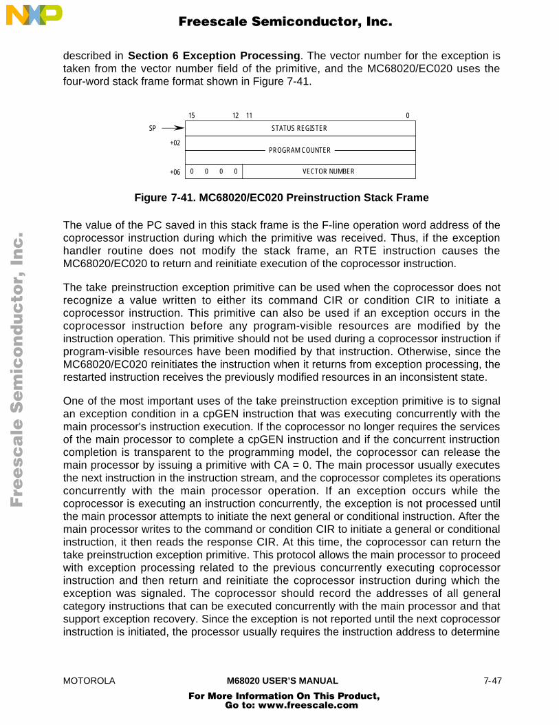
MOTOROLA M68020 USER’S MANUAL 7-47
described in Section 6 Exception Processing. The vector number for the exception istaken from the vector number field of the primitive, and the MC68020/EC020 uses thefour-word stack frame format shown in Figure 7-41.
0111215
STATUS REGISTER
0 0 0 0 VECTOR NUMBER
PROGRAM COUNTER
+06
+02
SP
Figure 7-41. MC68020/EC020 Preinstruction Stack Frame
The value of the PC saved in this stack frame is the F-line operation word address of thecoprocessor instruction during which the primitive was received. Thus, if the exceptionhandler routine does not modify the stack frame, an RTE instruction causes theMC68020/EC020 to return and reinitiate execution of the coprocessor instruction.
The take preinstruction exception primitive can be used when the coprocessor does notrecognize a value written to either its command CIR or condition CIR to initiate acoprocessor instruction. This primitive can also be used if an exception occurs in thecoprocessor instruction before any program-visible resources are modified by theinstruction operation. This primitive should not be used during a coprocessor instruction ifprogram-visible resources have been modified by that instruction. Otherwise, since theMC68020/EC020 reinitiates the instruction when it returns from exception processing, therestarted instruction receives the previously modified resources in an inconsistent state.
One of the most important uses of the take preinstruction exception primitive is to signalan exception condition in a cpGEN instruction that was executing concurrently with themain processor's instruction execution. If the coprocessor no longer requires the servicesof the main processor to complete a cpGEN instruction and if the concurrent instructioncompletion is transparent to the programming model, the coprocessor can release themain processor by issuing a primitive with CA = 0. The main processor usually executesthe next instruction in the instruction stream, and the coprocessor completes its operationsconcurrently with the main processor operation. If an exception occurs while thecoprocessor is executing an instruction concurrently, the exception is not processed untilthe main processor attempts to initiate the next general or conditional instruction. After themain processor writes to the command or condition CIR to initiate a general or conditionalinstruction, it then reads the response CIR. At this time, the coprocessor can return thetake preinstruction exception primitive. This protocol allows the main processor to proceedwith exception processing related to the previous concurrently executing coprocessorinstruction and then return and reinitiate the coprocessor instruction during which theexception was signaled. The coprocessor should record the addresses of all generalcategory instructions that can be executed concurrently with the main processor and thatsupport exception recovery. Since the exception is not reported until the next coprocessorinstruction is initiated, the processor usually requires the instruction address to determine
Fre
esc
ale
Se
mic
on
du
cto
r, I
Freescale Semiconductor, Inc.
For More Information On This Product, Go to: www.freescale.com
nc
...
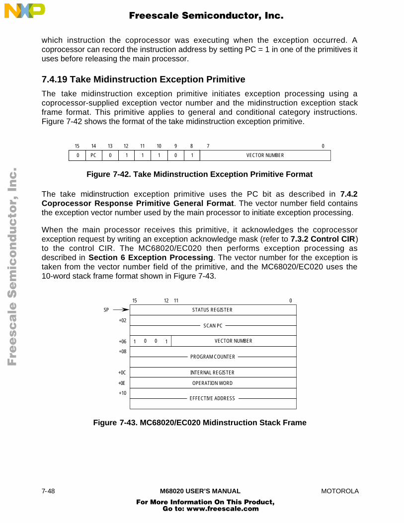
7-48 M68020 USER’S MANUAL MOTOROLA
which instruction the coprocessor was executing when the exception occurred. Acoprocessor can record the instruction address by setting PC = 1 in one of the primitives ituses before releasing the main processor.
7.4.19 Take Midinstruction Exception Primitive
The take midinstruction exception primitive initiates exception processing using acoprocessor-supplied exception vector number and the midinstruction exception stackframe format. This primitive applies to general and conditional category instructions.Figure 7-42 shows the format of the take midinstruction exception primitive.
15 0
0 PC 0
14 13 12
1 1
11 10 9 8 7
VECTOR NUMBER1 0 1
Figure 7-42. Take Midinstruction Exception Primitive Format
The take midinstruction exception primitive uses the PC bit as described in 7.4.2Coprocessor Response Primitive General Format. The vector number field containsthe exception vector number used by the main processor to initiate exception processing.
When the main processor receives this primitive, it acknowledges the coprocessorexception request by writing an exception acknowledge mask (refer to 7.3.2 Control CIR)to the control CIR. The MC68020/EC020 then performs exception processing asdescribed in Section 6 Exception Processing. The vector number for the exception istaken from the vector number field of the primitive, and the MC68020/EC020 uses the10-word stack frame format shown in Figure 7-43.
0111215
STATUS REGISTER
1 0 0 1 VECTOR NUMBER
SCAN PC
+06
+02
SP
PROGRAM COUNTER
+0C
OPERATION WORD
EFFECTIVE ADDRESS+10
INTERNAL REGISTER
+08
+0E
Figure 7-43. MC68020/EC020 Midinstruction Stack Frame
Fre
esc
ale
Se
mic
on
du
cto
r, I
Freescale Semiconductor, Inc.
For More Information On This Product, Go to: www.freescale.com
nc
...
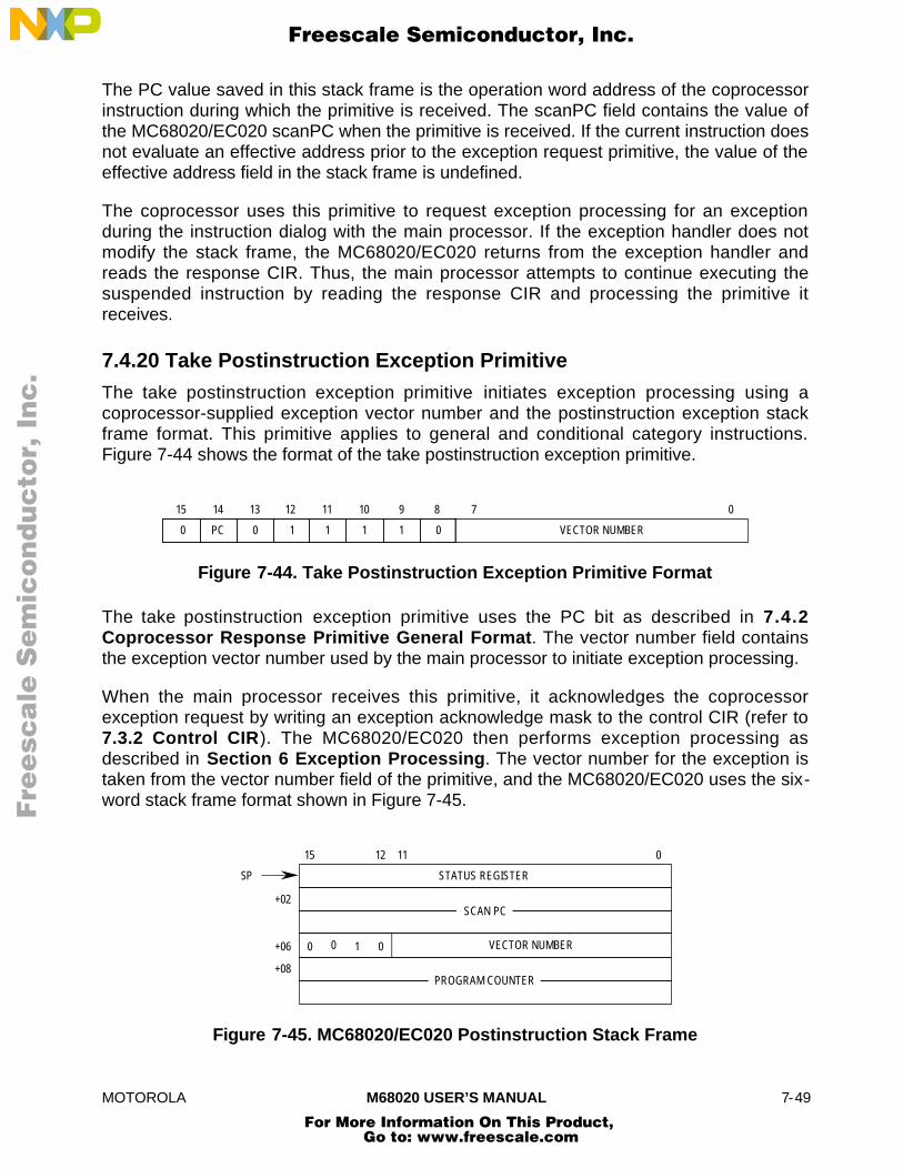
MOTOROLA M68020 USER’S MANUAL 7-49
The PC value saved in this stack frame is the operation word address of the coprocessorinstruction during which the primitive is received. The scanPC field contains the value ofthe MC68020/EC020 scanPC when the primitive is received. If the current instruction doesnot evaluate an effective address prior to the exception request primitive, the value of theeffective address field in the stack frame is undefined.
The coprocessor uses this primitive to request exception processing for an exceptionduring the instruction dialog with the main processor. If the exception handler does notmodify the stack frame, the MC68020/EC020 returns from the exception handler andreads the response CIR. Thus, the main processor attempts to continue executing thesuspended instruction by reading the response CIR and processing the primitive itreceives.
7.4.20 Take Postinstruction Exception Primitive
The take postinstruction exception primitive initiates exception processing using acoprocessor-supplied exception vector number and the postinstruction exception stackframe format. This primitive applies to general and conditional category instructions.Figure 7-44 shows the format of the take postinstruction exception primitive.
15 0
0 PC 0
14 13 12
1 1
11 10 9 8 7
VECTOR NUMBER1 1 0
Figure 7-44. Take Postinstruction Exception Primitive Format
The take postinstruction exception primitive uses the PC bit as described in 7.4.2Coprocessor Response Primitive General Format. The vector number field containsthe exception vector number used by the main processor to initiate exception processing.
When the main processor receives this primitive, it acknowledges the coprocessorexception request by writing an exception acknowledge mask to the control CIR (refer to7.3.2 Control CIR). The MC68020/EC020 then performs exception processing asdescribed in Section 6 Exception Processing. The vector number for the exception istaken from the vector number field of the primitive, and the MC68020/EC020 uses the six-word stack frame format shown in Figure 7-45.
0111215
STATUS REGISTER
0 0 1 0 VECTOR NUMBER
SCAN PC
+06
+02
SP
PROGRAM COUNTER+08
Figure 7-45. MC68020/EC020 Postinstruction Stack Frame
Fre
esc
ale
Se
mic
on
du
cto
r, I
Freescale Semiconductor, Inc.
For More Information On This Product, Go to: www.freescale.com
nc
...
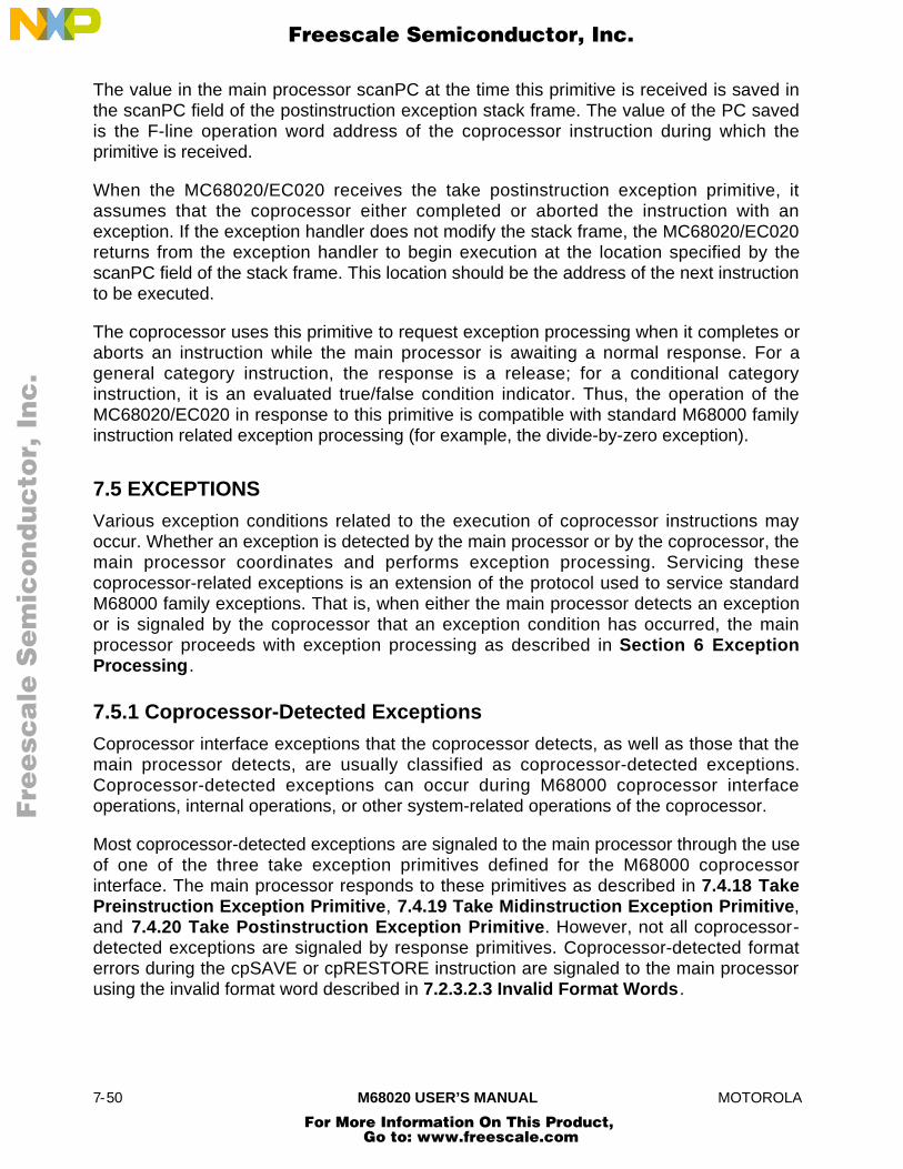
7-50 M68020 USER’S MANUAL MOTOROLA
The value in the main processor scanPC at the time this primitive is received is saved inthe scanPC field of the postinstruction exception stack frame. The value of the PC savedis the F-line operation word address of the coprocessor instruction during which theprimitive is received.
When the MC68020/EC020 receives the take postinstruction exception primitive, itassumes that the coprocessor either completed or aborted the instruction with anexception. If the exception handler does not modify the stack frame, the MC68020/EC020returns from the exception handler to begin execution at the location specified by thescanPC field of the stack frame. This location should be the address of the next instructionto be executed.
The coprocessor uses this primitive to request exception processing when it completes oraborts an instruction while the main processor is awaiting a normal response. For ageneral category instruction, the response is a release; for a conditional categoryinstruction, it is an evaluated true/false condition indicator. Thus, the operation of theMC68020/EC020 in response to this primitive is compatible with standard M68000 familyinstruction related exception processing (for example, the divide-by-zero exception).
7.5 EXCEPTIONS
Various exception conditions related to the execution of coprocessor instructions mayoccur. Whether an exception is detected by the main processor or by the coprocessor, themain processor coordinates and performs exception processing. Servicing thesecoprocessor-related exceptions is an extension of the protocol used to service standardM68000 family exceptions. That is, when either the main processor detects an exceptionor is signaled by the coprocessor that an exception condition has occurred, the mainprocessor proceeds with exception processing as described in Section 6 ExceptionProcessing.
7.5.1 Coprocessor-Detected Exceptions
Coprocessor interface exceptions that the coprocessor detects, as well as those that themain processor detects, are usually classified as coprocessor-detected exceptions.Coprocessor-detected exceptions can occur during M68000 coprocessor interfaceoperations, internal operations, or other system-related operations of the coprocessor.
Most coprocessor-detected exceptions are signaled to the main processor through the useof one of the three take exception primitives defined for the M68000 coprocessorinterface. The main processor responds to these primitives as described in 7.4.18 TakePreinstruction Exception Primitive, 7.4.19 Take Midinstruction Exception Primitive,and 7.4.20 Take Postinstruction Exception Primitive. However, not all coprocessor-detected exceptions are signaled by response primitives. Coprocessor-detected formaterrors during the cpSAVE or cpRESTORE instruction are signaled to the main processorusing the invalid format word described in 7.2.3.2.3 Invalid Format Words.
Fre
esc
ale
Se
mic
on
du
cto
r, I
Freescale Semiconductor, Inc.
For More Information On This Product, Go to: www.freescale.com
nc
...
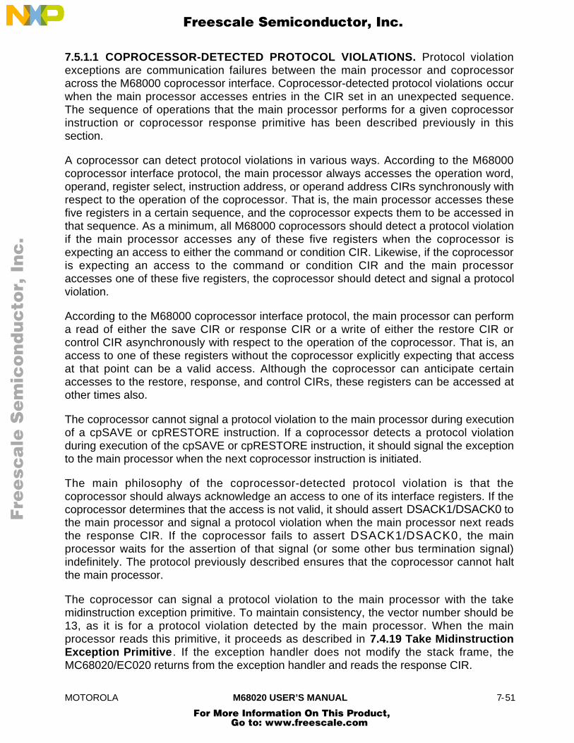
MOTOROLA M68020 USER’S MANUAL 7-51
7.5.1.1 COPROCESSOR-DETECTED PROTOCOL VIOLATIONS. Protocol violationexceptions are communication failures between the main processor and coprocessoracross the M68000 coprocessor interface. Coprocessor-detected protocol violations occurwhen the main processor accesses entries in the CIR set in an unexpected sequence.The sequence of operations that the main processor performs for a given coprocessorinstruction or coprocessor response primitive has been described previously in thissection.
A coprocessor can detect protocol violations in various ways. According to the M68000coprocessor interface protocol, the main processor always accesses the operation word,operand, register select, instruction address, or operand address CIRs synchronously withrespect to the operation of the coprocessor. That is, the main processor accesses thesefive registers in a certain sequence, and the coprocessor expects them to be accessed inthat sequence. As a minimum, all M68000 coprocessors should detect a protocol violationif the main processor accesses any of these five registers when the coprocessor isexpecting an access to either the command or condition CIR. Likewise, if the coprocessoris expecting an access to the command or condition CIR and the main processoraccesses one of these five registers, the coprocessor should detect and signal a protocolviolation.
According to the M68000 coprocessor interface protocol, the main processor can performa read of either the save CIR or response CIR or a write of either the restore CIR orcontrol CIR asynchronously with respect to the operation of the coprocessor. That is, anaccess to one of these registers without the coprocessor explicitly expecting that accessat that point can be a valid access. Although the coprocessor can anticipate certainaccesses to the restore, response, and control CIRs, these registers can be accessed atother times also.
The coprocessor cannot signal a protocol violation to the main processor during executionof a cpSAVE or cpRESTORE instruction. If a coprocessor detects a protocol violationduring execution of the cpSAVE or cpRESTORE instruction, it should signal the exceptionto the main processor when the next coprocessor instruction is initiated.
The main philosophy of the coprocessor-detected protocol violation is that thecoprocessor should always acknowledge an access to one of its interface registers. If thecoprocessor determines that the access is not valid, it should assert DSACK1/DSACK0 tothe main processor and signal a protocol violation when the main processor next readsthe response CIR. If the coprocessor fails to assert DSACK1/DSACK0, the mainprocessor waits for the assertion of that signal (or some other bus termination signal)indefinitely. The protocol previously described ensures that the coprocessor cannot haltthe main processor.
The coprocessor can signal a protocol violation to the main processor with the takemidinstruction exception primitive. To maintain consistency, the vector number should be13, as it is for a protocol violation detected by the main processor. When the mainprocessor reads this primitive, it proceeds as described in 7.4.19 Take MidinstructionException Primitive. If the exception handler does not modify the stack frame, theMC68020/EC020 returns from the exception handler and reads the response CIR.
Fre
esc
ale
Se
mic
on
du
cto
r, I
Freescale Semiconductor, Inc.
For More Information On This Product, Go to: www.freescale.com
nc
...

7-52 M68020 USER’S MANUAL MOTOROLA
7.5.1.2 COPROCESSOR-DETECTED ILLEGAL COMMAND OR CONDITION WORDS.Illegal coprocessor command or condition words are values written to the command CIRor condition CIR that the coprocessor does not recognize. If a value written to either ofthese registers is not valid, the coprocessor should return the take preinstructionexception primitive in the response CIR. When it receives this primitive, the mainprocessor takes a preinstruction exception as described in 7.4.18 Take PreinstructionException Primitive. If the exception handler does not modify the main processor stackframe, an RTE instruction causes the MC68020/EC020 to reinitiate the instruction thattook the exception. The coprocessor designer should ensure that the state of thecoprocessor is not irrecoverably altered by an illegal command or condition exception ifthe system supports emulation of the unrecognized command or condition word.
All M68000 coprocessors signal illegal command and condition words by returning thetake preinstruction exception primitive with the F-line emulator exception vector number11.
7.5.1.3 COPROCESSOR DATA-PROCESSING-RELATED EXCEPTIONS. Exceptionsrelated to the internal operation of a coprocessor are classified as data-processing-relatedexceptions. These exceptions are analogous to the divide-by-zero exception defined byM68000 microprocessors and should be signaled to the main processor using one of thethree take exception primitives containing an appropriate exception vector number. Whichof these three primitives is used to signal the exception is usually determined by the pointin the instruction operation where the main processor should continue the program flowafter exception processing. Refer to 7.4.18 Take Preinstruction Exception Primitives,7.4.19 Take Midinstruction Exception Primitive, and 7.4.20 Take PostinstructionException Primitive.
7.5.1.4 COPROCESSOR SYSTEM-RELATED EXCEPTIONS. System-related exceptionsdetected by a DMA coprocessor include those associated with bus activity and any otherexceptions (interrupts, for example) occurring external to the coprocessor. The actionstaken by the coprocessor and the main processor depend on the type of exception thatoccurs.
When an address or bus error is detected by a DMA coprocessor, the coprocessor shouldstore any information necessary for the main processor exception handling routines insystem-accessible registers. The coprocessor should place one of the three takeexception primitives encoded with an appropriate exception vector number in theresponse CIR. Which of the three primitives is used depends upon the point in thecoprocessor instruction at which the exception was detected and the point in theinstruction execution at which the main processor should continue after exceptionprocessing. Refer to 7.4.18 Take Preinstruction Exception Primitives, 7.4.19 TakeMidinstruction Exception Primitive, and 7.4.20 Take Postinstruction ExceptionPrimitive.
Fre
esc
ale
Se
mic
on
du
cto
r, I
Freescale Semiconductor, Inc.
For More Information On This Product, Go to: www.freescale.com
nc
...
MOTOROLA M68020 USER’S MANUAL 7-53
7.5.1.5 FORMAT ERRORS. Format errors are the only coprocessor-detected exceptionsthat are not signaled to the main processor with a response primitive. When the mainprocessor writes a format word to the restore CIR during the execution of a cpRESTOREinstruction, the coprocessor decodes this word to determine if it is valid (refer to 7.2.3.3Coprocessor Context Save Instruction). If the format word is not valid, the coprocessorplaces the invalid format code in the restore CIR. When the main processor reads theinvalid format code, it aborts the coprocessor instruction by writing an abort mask to thecontrol CIR (refer to 7.3.2 Control CIR). The main processor then performs exceptionprocessing using a four-word preinstruction stack frame and the format error exceptionvector number 14. Thus, if the exception handler does not modify the stack frame, theMC68020/EC020 restarts the cpRESTORE instruction when the RTE instruction in thehandler is executed. If the coprocessor returns the invalid format code when the mainprocessor reads the save CIR to initiate a cpSAVE instruction, the main processorperforms format error exception processing as outlined for the cpRESTORE instruction.
7.5.2 Main-Processor-Detected Exceptions
A number of exceptions related to coprocessor instruction execution are detected andserviced by the main processor instead of the coprocessor. These exceptions can berelated to the execution of coprocessor response primitives, communication across theM68000 coprocessor interface, or completion of conditional coprocessor instructions bythe main processor.
7.5.2.1 PROTOCOL VIOLATIONS. The main processor detects a protocol violation whenit reads a primitive from the response CIR that is not a valid primitive. The protocolviolations that can occur in response to the primitives defined for the M68000 coprocessorinterface are summarized in Table 7-6.
Fre
esc
ale
Se
mic
on
du
cto
r, I
Freescale Semiconductor, Inc.
For More Information On This Product, Go to: www.freescale.com
nc
...

7-54 M68020 USER’S MANUAL MOTOROLA
Table 7-6. Exceptions Related to Primitive Processing
Primitive Protocol F-Line Other
Busy
Null
Supervisory Check*Other: Privilege Violation if S-Bit in the SR = 0 X
Transfer Operation Word*
Transfer from Instruction Stream*Protocol: If Length Field Is Odd (Zero Length Legal) X
Evaluate and Transfer Effective AddressProtocol: If Used with Conditional InstructionF-Line: If EA in Opword Is NOT Control Alterable
XX
Evaluate Effective Address and Transfer DataProtocol:
1. If Used with Conditional Instructions2. Length Is Not 1, 2, or 4 and EA = Register Direct3. If EA = Immediate and Length Odd and Greater Than 14. Attempt to Write to Unalterable Address
Even if Address Declared Legal in PrimitiveF-Line: Valid EA Field Does Not Match EA in Opword
X
X
Write to Previously Evaluated Effective AddressProtocol: If Used with Conditional Instruction X
Take Address and Transfer Data*
Transfer to/from Top of Stack*Protocol: Length Field Other Than 1, 2, or 4 X
Transfer Single Main Processor Register*
Transfer Main Processor Control RegisterProtocol: Invalid Control Register Select Code X
Transfer Multiple Main Processor Registers*
Transfer Multiple Coprocessor RegistersProtocol:
1. If Used with Conditional Instructions2. Odd Length Value
F-Line:1. EA Not Control Alterable or (An)+ for CP to Memory Transfer2. EA Not Control Alterable or –(An) for Memory to CP Transfer
X
X
Transfer Status and ScanPCProtocol: If Used with Conditional InstructionOther:
1. Trace—Trace Made Pending if MC68020/EC020 in “Trace on Change ofFlow” Mode and DR = 1
2. Address Error—If Odd Value Written to ScanPC
XX
Take Preinstruction, Midinstruction, or Postinstruction ExceptionException Depends on Vector Supplies in Primitive
X X X
*Use of this primitive with CA = 0 will cause protocol violation on conditional instructions.Abbreviations:
EA—Effective AddressCP—Coprocessor
Fre
esc
ale
Se
mic
on
du
cto
r, I
Freescale Semiconductor, Inc.
For More Information On This Product, Go to: www.freescale.com
nc
...
MOTOROLA M68020 USER’S MANUAL 7-55
When the MC68020/EC020 detects a protocol violation, it does not automatically notify thecoprocessor of the resulting exception by writing to the control CIR. However, theexception handling routine may use the MOVES instruction to read the response CIR andthus determine the primitive that caused the MC68020/EC020 to initiate protocol violationexception processing. The main processor initiates exception processing using themidinstruction stack frame (refer to Figure 7-43) and the coprocessor protocol violationexception vector number 13. If the exception handler does not modify the stack frame, themain processor reads the response CIR again following the execution of an RTEinstruction to return from the exception handler. This protocol allows extensions to theM68000 coprocessor interface to be emulated in software by a main processor that doesnot provide hardware support for these extensions. Thus, the protocol violation istransparent to the coprocessor if the primitive execution can be emulated in software bythe main processor.
7.5.2.2 F-LINE EMULATOR EXCEPTIONS. The F-line emulator exceptions detected bythe MC68020/EC020 are either explicitly or implicitly related to the encodings of F-lineoperation words in the instruction stream. If the main processor determines that an F-lineoperation word is not valid, it initiates F-line emulator exception processing. Any F-lineoperation word with bits 8–6 = 110 or 111 causes the MC68020/EC020 to initiateexception processing without initiating any communication with the coprocessor for thatinstruction. Also, an operation word with bits 8–6 = 000–101 that does not map to one ofthe valid coprocessor instructions in the instruction set causes the MC68020/EC020 toinitiate F-line emulator exception processing. If the F-line emulator exception is either ofthese two situations, the main processor does not write to the control CIR prior to initiatingexception processing.
F-line exceptions can also occur if the operations requested by a coprocessor responseprimitive are not compatible with the effective address type in bits 5–0 of the coprocessorinstruction operation word. The F-line emulator exceptions that can result from the use ofthe M68000 coprocessor response primitives are summarized in Table 7-6. If theexception is caused by receiving an invalid primitive, the main processor aborts thecoprocessor instruction in progress by writing an abort mask (refer to 7.3.2 Control CIR)to the control CIR prior to F-line emulator exception processing.
Another type of F-line emulator exception occurs when a bus error occurs during the CIRaccess that initiates a coprocessor instruction. The main processor assumes that thecoprocessor is not present and takes the exception.
When the main processor initiates F-line emulator exception processing, it uses the four-word preinstruction exception stack frame (refer to Figure 7-41) and the F-line emulatorexception vector number 11. Thus, if the exception handler does not modify the stackframe, the main processor attempts to restart the instruction that caused the exceptionafter it executes an RTE instruction to return from the exception handler.
If the cause of the F-line exception can be emulated in software, the handler stores theresults of the emulation in the appropriate registers of the programming model and in thestatus register field of the saved stack frame. The exception handler adjusts the program
Fre
esc
ale
Se
mic
on
du
cto
r, I
Freescale Semiconductor, Inc.
For More Information On This Product, Go to: www.freescale.com
nc
...
7-56 M68020 USER’S MANUAL MOTOROLA
counter field of the saved stack frame to point to the next instruction operation word andexecutes the RTE instruction. The MC68020/EC020 then executes the instructionfollowing the instruction that was emulated.
The exception handler should also check the copy of the SR on the stack to determinewhether tracing is enabled. If tracing is enabled, the trace exception processing shouldalso be emulated. Refer to Section 6 Exception Processing for additional information.
7.5.2.3 PRIVILEGE VIOLATIONS. Privilege violations can result from the cpSAVE andcpRESTORE instructions and from the supervisor check coprocessor response primitive.The MC68020/EC020 initiates privilege violation exception processing if it attempts toexecute either the cpSAVE or cpRESTORE instruction when it is in the user state (S = 0in the SR). The main processor initiates this exception processing prior to anycommunication with the coprocessor associated with the cpSAVE or cpRESTOREinstructions.
If the main processor is executing a coprocessor instruction in the user state when it readsthe supervisor check primitive, it aborts the coprocessor instruction in progress by writingan abort mask to the control CIR (refer to 7.3.2 Control CIR). The main processor thenperforms privilege violation exception processing.
If a privilege violation occurs, the main processor initiates exception processing using thefour-word preinstruction stack frame (refer to Figure 7-41) and the privilege violationexception vector number 8. Thus, if the exception handler does not modify the stackframe, the main processor attempts to restart the instruction during which the exceptionoccurred after it executes an RTE to return from the handler.
7.5.2.4 cpTRAPcc INSTRUCTION TRAPS. If, during the execution of a cpTRAPccinstruction, the coprocessor returns the TRUE condition indicator to the main processorwith a null primitive, the main processor initiates trap exception processing. The mainprocessor uses the six-word postinstruction exception stack frame (refer to Figure 7-45)and the trap exception vector number 7. The scanPC field of this stack frame contains theaddress of the instruction following the cpTRAPcc instruction. The processing associatedwith the cpTRAPcc instruction can then proceed, and the exception handler can locateany immediate operand words encoded in the cpTRAPcc instruction using the informationcontained in the six-word stack frame. If the exception handler does not modify the stackframe, the main processor executes the instruction following the cpTRAPcc instructionafter it executes an RTE instruction to exit from the handler.
7.5.2.5 TRACE EXCEPTIONS. The MC68020/EC020 supports two modes of instructiontracing, as discussed in Section 6 Exception Processing . In the trace on instructionexecution mode, the MC68020/EC020 takes a trace exception after completing eachinstruction. In the trace on change of flow mode, the MC68020/EC020 takes a traceexception after each instruction that alters the SR or places an address other than theaddress of the next instruction in the PC.
Fre
esc
ale
Se
mic
on
du
cto
r, I
Freescale Semiconductor, Inc.
For More Information On This Product, Go to: www.freescale.com
nc
...

MOTOROLA M68020 USER’S MANUAL 7-57
The protocol used to execute coprocessor cpSAVE, cpRESTORE, or conditional categoryinstructions does not change when a trace exception is pending in the main processor.The main processor performs a pending trace on instruction execution exception aftercompleting the execution of that instruction. If the main processor is in the trace onchange of flow mode and an instruction places an address other than that of the nextinstruction in the PC, the processor takes a trace exception after it executes theinstruction.
If a trace exception is not pending during a general category instruction, the mainprocessor terminates communication with the coprocessor after reading any primitive withCA = 0. Thus, the coprocessor can complete a cpGEN instruction concurrently with theexecution of instructions by the main processor. When a trace exception is pending,however, the main processor must ensure that all processing associated with a cpGENinstruction has been completed before it takes the trace exception. In this case, the mainprocessor continues to read the response CIR and to service the primitives until it receiveseither a null primitive with CA = 0 and PF = 1 or until exception processing caused by atake postinstruction exception primitive has completed. The coprocessor should return thenull primitive with CA = 0 and PF = 0 while it is completing the execution of the cpGENinstruction. The main processor may service pending interrupts between reads of theresponse CIR if IA = 1 in these primitives (refer to Table 7-3). This protocol ensures that atrace exception is not taken until all processing associated with a cpGEN instruction hascompleted.
If T1, T0 = 01 in the MC68020/EC020 SR (trace on change of flow mode) when a generalcategory instruction is initiated, a trace exception is taken for the instruction only when thecoprocessor issues a transfer status register and scanPC primitive with DR = 1 during theexecution of that instruction. In this case, it is possible that the coprocessor is stillexecuting the cpGEN instruction concurrently when the main processor begins executionof the trace exception handler. A cpSAVE instruction executed during the trace on changeof flow exception handler could thus suspend the execution of a concurrently operatingcpGEN instruction.
7.5.2.6 INTERRUPTS. Interrupt processing, discussed in Section 6 ExceptionProcessing, can occur at any instruction boundary. Interrupts are also serviced during theexecution of a general or conditional category instruction under either of two conditions. Ifthe main processor reads a null primitive with CA = 1 and IA = 1, it services any pendinginterrupts prior to reading the response CIR. Similarly, if a trace exception is pendingduring cpGEN instruction execution and the main processor reads a null primitive with CA= 0, IA = 1, and PF = 0 (refer to 7.5.2.5 Trace Exceptions), the main processor servicespending interrupts prior to reading the response CIR again.
The MC68020/EC020 uses the 10-word midinstruction stack frame (see Figure 7-43)when it services interrupts during the execution of a general or conditional categorycoprocessor instruction. Since it uses this stack frame, the main processor can perform allnecessary processing and then return to read the response CIR. Thus, it can continueexecution of the coprocessor instruction during which the interrupt exception occurred.
Fre
esc
ale
Se
mic
on
du
cto
r, I
Freescale Semiconductor, Inc.
For More Information On This Product, Go to: www.freescale.com
nc
...

7-58 M68020 USER’S MANUAL MOTOROLA
The MC68020/EC020 also services interrupts if it reads the not-ready format word fromthe save CIR during a cpSAVE instruction. The MC68020/EC020 uses the normal four-word preinstruction stack frame (see Figure 7-41) when it services interrupts after readingthe not-ready format word. Thus, the processor can service any pending interrupts andexecute an RTE to return and reinitiate the cpSAVE instruction by reading the save CIR.
7.5.2.7 FORMAT ERRORS. The MC68020/EC020 can detect a format error whileexecuting a cpSAVE or cpRESTORE instruction if the length field of a valid format word isnot a multiple of four bytes. If the MC68020/EC020 reads a format word with an invalidlength field from the save CIR during the cpSAVE instruction, it aborts the coprocessorinstruction by writing an abort mask to the control CIR (refer to 7.3.2 Control CIR) andinitiates format error exception processing. If the MC68020/EC020 reads a format wordwith an invalid length field from the effective address specified in the cpRESTOREinstruction, the MC68020/EC020 writes that format word to the restore CIR and then readsthe coprocessor response from the restore CIR. The MC68020/EC020 then aborts thecpRESTORE instruction by writing an abort mask to the control CIR (refer to 7.3.2Control CIR) and initiates format error exception processing.
The MC68020/EC020 uses the four-word preinstruction stack frame (see Figure 7-41) andthe format error vector number 14 when it initiates format error exception processing.Thus, if the exception handler does not modify the stack frame, the main processor, after itexecutes an RTE to return from the handler, attempts to restart the instruction duringwhich the exception occurred.
7.5.2.8 ADDRESS AND BUS ERRORS. Coprocessor-instruction-related bus faults canoccur during main processor bus cycles to CPU space to communicate with a coprocessoror during memory cycles run as part of the coprocessor instruction execution. If a buserror occurs during the CIR access that is used to initiate a coprocessor instruction, themain processor assumes that the coprocessor is not present and takes an F-line emulatorexception as described in 7.5.2.2 F-Line Emulator Exceptions. That is, the processortakes an F-line emulator exception when a bus error occurs during the initial access to aCIR by a coprocessor instruction. If a bus error occurs on any other coprocessor accessor on a memory access made during the execution of a coprocessor instruction, the mainprocessor performs bus error exception processing as described in Section 6 ExceptionProcessing. After the exception handler has corrected the cause of the bus error, themain processor can return to the point in the coprocessor instruction at which the faultoccurred.
An address error occurs if the MC68020/EC020 attempts to prefetch an instruction froman odd address. This can occur if the calculated destination address of a cpBcc or cpDBccinstruction is odd or if an odd value is transferred to the scanPC with the transfer statusregister and the scanPC response primitive. If an address error occurs, theMC68020/EC020 performs exception processing for a bus fault as described in Section 6Exception Processing.
Fre
esc
ale
Se
mic
on
du
cto
r, I
Freescale Semiconductor, Inc.
For More Information On This Product, Go to: www.freescale.com
nc
...

MOTOROLA M68020 USER’S MANUAL 7-59
7.5.3 Coprocessor Reset
Either an external reset signal or a RESET instruction can reset the external devices of asystem. The system designer can design a coprocessor to be reset and initialized by bothreset types or by external reset signals only. To be consistent with the MC68020/EC020design, the coprocessor should be affected by external reset signals only and not byRESET instructions, because the coprocessor is an extension to the main processorprogramming model and to the internal state of the MC68020/EC020.
7.6 COPROCESSOR SUMMARY
Coprocessor instruction formats are included with the instruction formats in theM68000PM/AD, M68000 Family Programmer's Reference Manual.
The M68000 coprocessor response primitive formats are shown in this section. Anyresponse primitive with bits 13–8 = $00 or $3F causes a protocol violation exception.Response primitives with bits 13–8 = $0B, $18–$1B, $1F, $28–$2B, and $38–3B currentlycause protocol violation exceptions; they are undefined and reserved for future use byMotorola.
Fre
esc
ale
Se
mic
on
du
cto
r, I
Freescale Semiconductor, Inc.
For More Information On This Product, Go to: www.freescale.com
nc
...
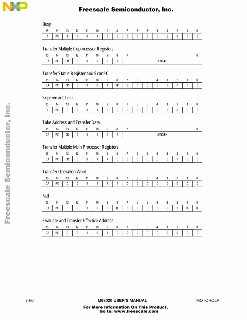
7-60 M68020 USER’S MANUAL MOTOROLA
15
1 PC 1
14 13 12
0 0
11 10 9 07
1 0
2
0
3
0
4
0
5
0
6
000
8
0 0
1
15
CA PC DR
14 13 12
0 0
11 10 9 07
0 0 LENGTH1
8
15
CA PC DR
14 13 12
0 0
11 10 9 07
0 1
2
0
3
0
4
0
5
0
6
00SP
8
0 0
1
15
1 PC 0
14 13 12
0 0
11 10 9 07
1 0
2
0
3
0
4
0
5
0
6
000
8
0 0
1
15
CA PC DR
14 13 12
0 0
11 10 9 07
1 1
2
0
3
0
4
0
5
0
6
000
8
0 0
1
15
CA PC 0
14 13 12
0 0
11 10 9 07
1 1
2
0
3
0
4
0
5
0
6
001
8
0 0
1
15
CA PC 0
14 13 12
0 1
11 10 9 07
0 0
2
PF
3
0
4
0
5
0
6
00IA
8
0 TF
1
15
CA PC 0
14 13 12
0 1
11 10 9 07
0 1
2
0
3
0
4
0
5
0
6
000
8
0 0
1
15
CA PC DR
14 13 12
0 0
11 10 9 07
1 0 LENGTH1
8
Busy
Transfer Multiple Coprocessor Registers
Transfer Status Register and ScanPC
Supervisor Check
Take Address and Transfer Data
Transfer Multiple Main Processor Registers
Transfer Operation Word
Null
Evaluate and Transfer Effective Address
Fre
esc
ale
Se
mic
on
du
cto
r, I
Freescale Semiconductor, Inc.
For More Information On This Product, Go to: www.freescale.com
nc
...

MOTOROLA M68020 USER’S MANUAL 7-61
15
CA PC DR
14 13 12
0 1
11 10 9 07
1 1 LENGTH0
8
15
CA PC DR
14 13 12
0 1
11 10 9 07
1 0
2
0
3
0
4
0
5
0
6
001
8
0 0
1
15
CA PC DR
14 13 12
0 1
11 10 9 07
1 0
2
REGISTER
3
D/A
4
0
5
0
6
000
8
15
CA PC 0
14 13 12
0 1
11 10 9 07
1 1 LENGTH1
8
15
CA PC DR
14 13 12
1 0
11 10 9 07
VALID EA LENGTH
8
15
0 PC 0
14 13 12
1 1
11 10 9 07
1 0 VECTOR NUMBER0
8
15
0 PC 0
14 13 12
1 1
11 10 9 07
1 0 VECTOR NUMBER1
8
15
0 PC 0
14 13 12
1 1
11 10 9 07
1 1 VECTOR NUMBER0
8
15
CA PC 1
14 13 12
0 0
11 10 9 07
0 0 LENGTH0
8
Transfer Single Main Processor Register
Transfer Main Processor Control Register
Transfer to/from Top of Stack
Transfer from Instruction Stream
Evaluate Effective Address and Transfer Data
Take Preinstruction Exception
Take Midinstruction Exception
Take Postinstruction Exception
Write to Previously Evaluated Effective Address
Fre
esc
ale
Se
mic
on
du
cto
r, I
Freescale Semiconductor, Inc.
For More Information On This Product, Go to: www.freescale.com
nc
...

MOTOROLA M68020 USER’S MANUAL 8-1
SECTION 8INSTRUCTION EXECUTION TIMING
This section describes the instruction execution and operations (table searches, etc.) ofthe MC68020/EC020 in terms of external clock cycles. It provides accurate execution andoperation timing guidelines but not exact timings for every possible circumstance. Thisapproach is used since exact execution time for an instruction or operation is highlydependent on memory speeds and other variables. The timing numbers presented in thissection allow the assembly language programmer or compiler writer to predict timingsneeded to evaluate the performance of the MC68020/EC020.
In this section, instruction and operation times are shown in clock cycles, which eliminatesclock frequency dependencies.
8.1 TIMING ESTIMATION FACTORS
The advanced architecture of the MC68020/EC020 makes exact instruction timingcalculations difficult due to the effects of:
1. An On-Chip Instruction Cache and Instruction Prefetch
2. Operand Misalignment
3. Bus Controller/Sequence Concurrency
4. Instruction Execution Overlap
These factors make MC68020/EC020 instruction set timing difficult to calculate on a singleinstruction basis since instructions vary in execution time from one context to another. Adetailed explanation of each of these factors follows.
8.1.1 Instruction Cache and Prefetch
The on-chip cache of the MC68020/EC020 is an instruction-only cache. Its purpose is toincrease execution efficiency by providing a quick store for instructions.
Instruction prefetches that hit in the cache will occur with no delay in instruction execution.Instruction prefetches that miss in the cache will cause an external memory cycle to beperformed, which may overlap with internal instruction execution. Thus, while theexecution unit of the microprocessor is busy, the bus controller prefetches the nextinstruction from external memory. Both cases are illustrated in later examples.
Fre
esc
ale
Se
mic
on
du
cto
r, I
Freescale Semiconductor, Inc.
For More Information On This Product, Go to: www.freescale.com
nc
...
8-2 M68020 USER’S MANUAL MOTOROLA
When prefetching instructions from external memory, the microprocessor will utilize long-word read cycles. When the read is aligned on a long-word address boundary, theprocessor reads two words, which may load two instructions at once or two words of amultiword instruction. The subsequent instruction prefetch will find the second word isalready available, and there is no need to run an external bus cycle (read).
The MC68020/EC020 always prefetches long words. When an instruction prefetch falls onan odd-word boundary (e.g., due to a branch to an odd-word location), theMC68020/EC020 will read the even word associated with the long-word base address atthe same time as (32-bit memory) or before (8- or 16-bit memory) the odd word is read.When an instruction prefetch falls on an even-word boundary (as would be the normalcase), the MC68020/EC020 reads both words at the long-word address, thus effectivelyprefetching the next two words.
8.1.2 Operand Misalignment
Another significant factor affecting instruction timing is operand misalignment. Operandmisalignment has impact on performance when the microprocessor is reading or writingexternal memory. In this case, the address of a word operand falls across a long-wordboundary, or a long-word operand falls on a byte or word address that is not a long-wordboundary. Although the MC68020/EC020 will automatically handle all occurrences ofoperand misalignment, it must use multiple bus cycles to complete such transfers.
8.1.3 Bus/Sequencer Concurrency
The bus controller is responsible for all bus activity. The sequencer controls the buscontroller, instruction execution, and internal processor operation, such as calculation ofeffective addresses and setting of condition codes.
The bus controller and sequencer can operate on an instruction concurrently. The buscontroller can perform a read or write while the sequencer controls an effective addresscalculation or sets the condition codes. The sequencer may also request a bus cycle thatthe bus controller cannot immediately perform. In this case, the bus cycle is queued andthe bus controller runs the cycle when the current cycle is complete.
Fre
esc
ale
Se
mic
on
du
cto
r, I
Freescale Semiconductor, Inc.
For More Information On This Product, Go to: www.freescale.com
nc
...

MOTOROLA M68020 USER’S MANUAL 8-3
8.1.4 Instruction Execution Overlap
Overlap is the time, measured in clocks, when two instructions execute concurrently. InFigure 8-1, instructions A and B execute concurrently, and the overlapped portion ofinstruction B is absorbed in the instruction execution time of A (the previous instruction).The overlap time is deducted from the execution time of instruction B. Similarly, there is anoverlap period between instruction B and instruction C, which reduces the attributedexecution time for C.
INSTRUCTION A
INSTRUCTION B
INSTRUCTION C
OVERLAP OVERLAP
Figure 8-1. Concurrent Instruction Execution
The execution time attributed to instructions A, B, and C (after considering the overlap) isdepicted in Figure 8-2.
INSTRUCTION A
INSTRUCTION B
INSTRUCTION C
OVERLAPPERIOD
(ABSORBED BYINSTRUCTION B)
OVERLAPPERIOD
(ABSORBED BYINSTRUCTION A)
Figure 8-2. Instruction Execution for Instruction Timing Purposes
It is possible that the execution time of an instruction will be absorbed by the overlap witha previous instruction for a net execution time of zero clocks.
Because of this overlap, a NOP is required between a write to a peripheral to clear aninterrupt request and a subsequent MOVE to SR instruction to lower the interrupt masklevel. Otherwise, the MOVE to SR instruction may complete before the write isaccomplished, and a new interrupt exception will be generated for an old interrupt request.
Fre
esc
ale
Se
mic
on
du
cto
r, I
Freescale Semiconductor, Inc.
For More Information On This Product, Go to: www.freescale.com
nc
...

8-4 M68020 USER’S MANUAL MOTOROLA
8.1.5 Instruction Stream Timing Examples
A programming example allows a more detailed examination of these effects. The effect ofinstruction execution overlap on instruction timing is illustrated by the following exampleinstruction stream.
Instruction
#1) MOVE.L D4,(A1)+
#2) ADD.L D4,D5
#3) MOVE.L (A1), –(A2)
#4) ADD.L D5,D6
Example 1
For the first example, the assumptions are:1. The data bus is 32 bits,
2. The first instruction is prefetched from an odd-word address,
3. Memory access occurs with no wait states, and
4. The instruction cache is disabled.
For example 1, the instruction stream is positioned in 32-bit memory as follows:
Address n ••• MOVE #1
n + 4 ADD #2 MOVE #3
n + 8 ADD #4 •••
Figure 8-3 shows processor activity on the first example instruction stream. It shows theactivity of the external bus, the bus controller, the sequencer, and the attributed instructionexecution time.
Fre
esc
ale
Se
mic
on
du
cto
r, I
Freescale Semiconductor, Inc.
For More Information On This Product, Go to: www.freescale.com
nc
...

MOTOROLA M68020 USER’S MANUAL 8-5
1 2 3 4 5 6 7 8 9 10 11 12 13 14 15 16 17
CLOCK
BUS ACTIVITY
PREFETCH WRITE READ PREFETCH WRITE
PREFETCHBYTES n + 8
BUSCONTROLLER WRITE TO (A1)+ PREFETCH
BYTES n + 12 WRITE TO –(A2)READ FROM (A1) IDLE
PERFORMMOVE #1 IDLE PERFORM
ADD #2
CALCULATESOURCE EA
MOVE #3
CALCULATEDESTINATION
EAMOVE #3
IDLE PERFORMMOVE #3
PERFORMADD #4
MOVE.L D4,(A1)+ MOVE.L (A1),–(A2) ADD.LD5,D6
SEQUENCER
INSTRUCTION EXECUTION TIME
(6) (9) (1)CLOCKCOUNT
LEGEND:
1) MOVE.L D4,(A1)+
2) ADD.L D4,D5
3) MOVE.L (A1),–(A2)
4) ADD.L D5,D6
Figure 8-3. Processor Activity for Example 1
For the first three clocks of this example, the bus controller and sequencer are bothperforming tasks associated with the MOVE #1 instruction. The next three clocks (clocks4, 5, and 6) demonstrate instruction overlap. The bus controller is performing a write tomemory as part of the MOVE #1 instruction. The sequencer, on the other hand, isperforming the ADD #2 instruction for two clocks (clocks 4 and 5) and beginning sourceeffective address (EA) calculations for the MOVE #3 instruction. The bus controller activitycompletely overlaps the execution of the ADD #2 instruction, causing the ADD #2attributed execution time to be zero clocks. The overlap also shortens the effectiveexecution time of the MOVE #3 instruction by one clock because the bus controllercompletes the MOVE #1 write operation while the sequencer begins the MOVE #3 EAcalculation.
The sequencer continues the source EA calculation for one more clock period (clock 7)while the bus controller begins a read for MOVE #3. When counting instruction executiontime in bus clocks, the MOVE #1 completes at the end of clock 6, and the execution ofMOVE #3 begins on clock 7.
Both the sequencer and bus controller continue with MOVE #3 until the end of clock 14,when the sequencer begins to perform ADD #4. Timing for MOVE #3 continues becausethe bus controller is still performing the write to the destination of MOVE #3. The busactivity for MOVE #3 completes at the end of clock 15. The effective execution time forMOVE #3 is nine clocks.
The one clock cycle (clock 15) when the sequencer is performing ADD #4 and the buscontroller is writing to the destination of MOVE #3 is absorbed by the execution time ofMOVE #3. This overlap shortens the effective execution time of ADD #4 by one clock,giving it an attributed execution time of one clock.
Fre
esc
ale
Se
mic
on
du
cto
r, I
Freescale Semiconductor, Inc.
For More Information On This Product, Go to: www.freescale.com
nc
...
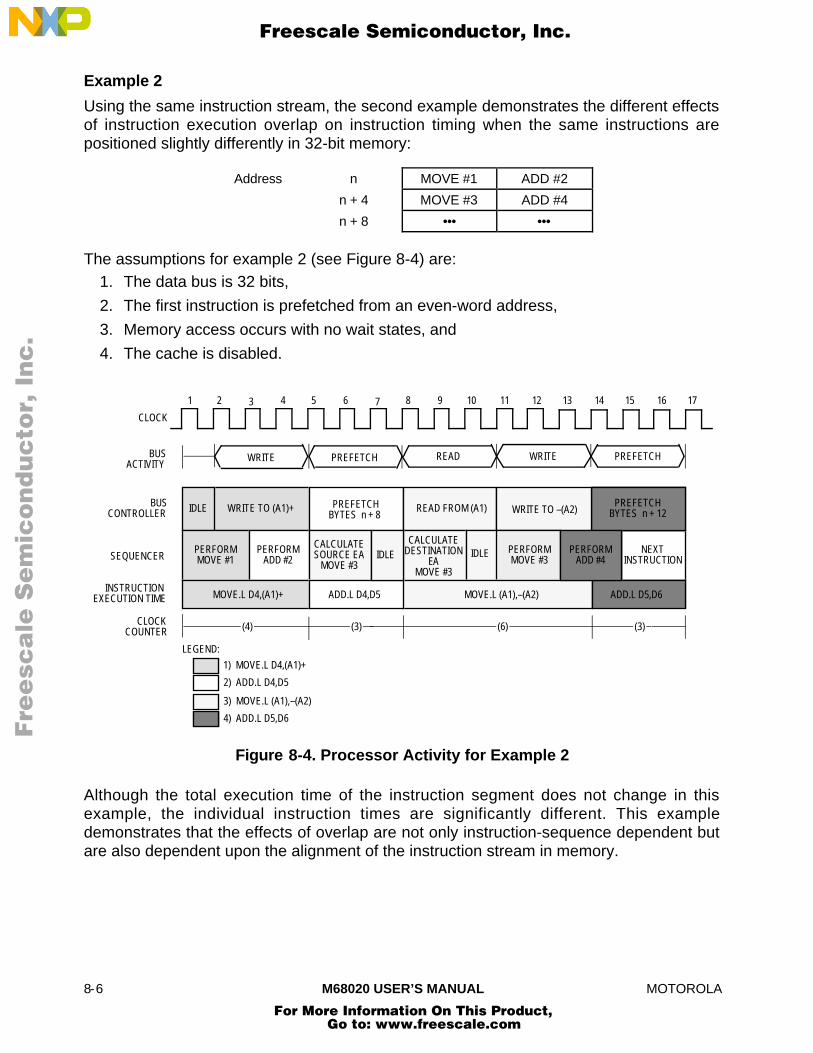
8-6 M68020 USER’S MANUAL MOTOROLA
Example 2
Using the same instruction stream, the second example demonstrates the different effectsof instruction execution overlap on instruction timing when the same instructions arepositioned slightly differently in 32-bit memory:
Address n MOVE #1 ADD #2
n + 4 MOVE #3 ADD #4
n + 8 ••• •••
The assumptions for example 2 (see Figure 8-4) are:1. The data bus is 32 bits,
2. The first instruction is prefetched from an even-word address,
3. Memory access occurs with no wait states, and
4. The cache is disabled.
1 2 3 4 5 6 7 8 9 10 11 12 13 14 15 16 17
CLOCK
BUS ACTIVITY
PREFETCHWRITE READ PREFETCHWRITE
PREFETCHBYTES n + 12
BUSCONTROLLER WRITE TO (A1)+ PREFETCH
BYTES n + 8 WRITE TO –(A2)READ FROM (A1)IDLE
PERFORMMOVE #1
PERFORMADD #2
CALCULATESOURCE EA
MOVE #3
CALCULATEDESTINATION
EAMOVE #3
PERFORMMOVE #3
MOVE.L D4,(A1)+ MOVE.L (A1),–(A2) ADD.L D5,D6
SEQUENCER
INSTRUCTION EXECUTION TIME
(4) (3) (3)CLOCKCOUNTER
LEGEND:
1) MOVE.L D4,(A1)+
2) ADD.L D4,D5
3) MOVE.L (A1),–(A2)
4) ADD.L D5,D6
IDLE NEXT INSTRUCTION
ADD.L D4,D5
(6)
PERFORMADD #4IDLE
Figure 8-4. Processor Activity for Example 2
Although the total execution time of the instruction segment does not change in thisexample, the individual instruction times are significantly different. This exampledemonstrates that the effects of overlap are not only instruction-sequence dependent butare also dependent upon the alignment of the instruction stream in memory.
Fre
esc
ale
Se
mic
on
du
cto
r, I
Freescale Semiconductor, Inc.
For More Information On This Product, Go to: www.freescale.com
nc
...

MOTOROLA M68020 USER’S MANUAL 8-7
Example 3
Both Figures 8-3 and 8-4 show instruction execution without benefit of theMC68020/EC020 instruction cache. Figure 8-5 shows a third example for the sameinstruction stream executing in the cache. Note that once the instructions are in the cache,the original location in external memory is no longer a factor in timing.
The assumptions for Example 3 are:1. The data bus is 32 bits,
2. The cache is enabled and instructions are in the cache, and
3. Memory access occurs with no wait states.
1 2 3 4 5 6 7 8 9 10 11 12 13
CLOCK
BUS ACTIVITY
WRITE READ WRITE
BUSCONTROLLER WRITE TO (A1)+ WRITE TO –(A2)READ FROM (A1)IDLE
PERFORMMOVE #1
PERFORMADD #2
CALCULATESOURCE EA
MOVE #3
CALCULATEDESTINATION
EAMOVE #3
PERFORMMOVE #3
MOVE.L D4,(A1)+ MOVE.L (A1),–(A2) ADD.LD5,D6
SEQUENCER
INSTRUCTION EXECUTION TIME
(4) (1)CLOCKCOUNTER
LEGEND:
1) MOVE.L D4,(A1)+
2) ADD.L D4,D5
3) MOVE.L (A1),–(A2)
4) ADD.L D5,D6
(7)
PERFORMADD #4
IDLE IDLE
Figure 8-5. Processor Activity for Example 3
Figure 8-5 illustrates the benefits of the instruction cache. The total number of clock cyclesis reduced from 16 to 12 clocks. Since the instructions are resident in the cache, theinstruction prefetch activity does not require the bus controller to perform external buscycles. Since prefetch occurs with no delay, the bus controller is idle more often.
Example 4
Idle clock cycles, such as those shown in example 3, are useful in MC68020/EC020systems that require wait states when accessing external memory. This fact is illustratedin example 4 (see Figure 8-6) with the following assumptions:
1. The data bus is 32 bits,
2. The cache is enabled and instructions are in the cache, and
3. Memory access occurs with one wait state.
Fre
esc
ale
Se
mic
on
du
cto
r, I
Freescale Semiconductor, Inc.
For More Information On This Product, Go to: www.freescale.com
nc
...

8-8 M68020 USER’S MANUAL MOTOROLA
1 2 3 4 5 6 7 8 9 10 11 12 13 14
CLOCK
BUS ACTIVITY
WRITE READ WRITE
BUSCONTROLLER
WRITE TO (A1)+ WRITE TO –(A2)READ FROM (A1)IDLE
PERFORMMOVE #1
PERFORMADD #2
CALCULATESOURCE EA
MOVE #3
PERFORMMOVE #3
MOVE.L D4,(A1)+ MOVE.L (A1),–(A2)
SEQUENCER
INSTRUCTION EXECUTION TIME
(5)CLOCKCOUNTER
LEGEND:
1) MOVE.L D4,(A1)+
2) ADD.L D4,D5
3) MOVE.L (A1),–(A2)
4) ADD.L D5,D6
IDLE PERFORMADD #4
(8)
CALCULATEDESTINATION
EAMOVE #3
Figure 8-6. Processor Activity for Example 4
Figure 8-6 shows the same instruction stream executing with four clocks for every readand write. The idle bus cycles coincide with the wait states of the memory access;therefore, the total execution time is only 13 clocks.
Examples 1–4 demonstrate the complexity of instruction timing calculation for theMC68020/EC020. It is impossible to anticipate individual instruction timing as an absolutenumber of clock cycles due to the dependency of overlap on the instruction sequence andalignment as well as the number of wait states in memory. This can be seen by comparingindividual and composite time for Figures 8-3 through 8-6. These instruction timings arecompared in Table 8-1, where timing varies for each instruction as the context varies.
Table 8-1. Examples 1–4 Instruction Stream Execution Comparison
InstructionExample 1
(Odd Alignment)Example 2
(Even Alignment)Example 3
(Cache)
Example 4(Cache withWait States)
#1) MOVE.L#2) ADD.L#3) MOVE.L#4) ADD.L
D4,(A1)+D4,D5(A1),–(A2)D5,D6
6091
4363
4071
5080
Total Clock Cycles 16 16 12 13
Fre
esc
ale
Se
mic
on
du
cto
r, I
Freescale Semiconductor, Inc.
For More Information On This Product, Go to: www.freescale.com
nc
...
MOTOROLA M68020 USER’S MANUAL 8-9
8.2 INSTRUCTION TIMING TABLES
The instruction times given in the following illustration include the following assumptionsabout the MC68020/EC020 system:
1. All operands are long-word aligned as is the stack,
2. The data bus is 32 bits, and
3. Memory access occurs with no wait states (three-cycle read/write).
There are three values given for each instruction and addressing mode:1. The best case (BC), which reflects the time (in clocks) when the instruction is in the
cache and benefits from maximum overlap due to other instructions,
2. The cache-only case (CC) when the instruction is in the cache but has no overlap,and
3. The worst case (WC) when the instruction is not in the cache or the cache isdisabled and there is no instruction overlap.
The only instances for which the size of the operand has any effect are the instructionswith immediate operands. Unless specified otherwise, immediate byte and word operandshave identical execution times.
Within each set or column of instruction timings are four sets of numbers, three of whichare enclosed in parentheses. The bolded outer number is the total number of clocks forthe instruction. The first number inside the parentheses is the number of operand readcycles performed by the instruction. The second value inside parentheses is the numberof instruction accesses performed by the instruction, including all prefetches to keep theinstruction pipe filled. The third value within parentheses is the number of write cyclesperformed by the instruction. One example from the instruction timing table is:
TOTAL NUMBER OF CLOCKS
NUMBER OF READ CYCLES
NUMBER OF INSTRUCTION ACCESS CYCLES
NUMBER OF WRITE CYCLES
24 (2 3 0)/ /
The total number of bus-activity clocks for the previous example is derived in the followingway:
(2 Reads * 3 Clocks/Read) + (3 Instruction Accesses * 3 Clocks/Access)+ (0 Writes * 3 Clocks/Write) = 15 Clocks of Bus Activity
24 Total Clocks – 15 Clocks (Bus Activity) = 9 Internal Clocks
The example used here was taken from a worst-case fetch effective address time. Theaddressing mode was ([d32,B],I,d32). The same addressing mode under the best-case
Fre
esc
ale
Se
mic
on
du
cto
r, I
Freescale Semiconductor, Inc.
For More Information On This Product, Go to: www.freescale.com
nc
...
8-10 M68020 USER’S MANUAL MOTOROLA
entry is 17 (2/0/0). For the best case, there are no instruction accesses because the cacheis enabled and the sequencer does not have to go to external memory for the instructionwords.
The first tables deal exclusively with fetching and calculating effective addresses andimmediate operands. The tables are arranged in this manner because some instructionsdo not require effective address calculation or fetching. For example, the instruction CLR<ea> (found in the table under 8.2.11 Single Operand Instructions) only needs to have acalculated effective address time added to its table entry because no fetch of an operandis required. This instruction only writes to memory or a register. Some instructions usespecific addressing modes which exclude timing for calculation or fetching of an operand.When these instances arise, they are footnoted to indicate which other tables are neededin the timing calculation.
Many two-word instructions (e.g., MULU.L, DIV.L, BFSET, etc.) include the fetchimmediate effective address time or the calculate immediate effective address time in theexecution time calculation. The timing for immediate data of word length (#<data>.W) isused for these calculations. If the instruction has a source and a destination, the sourceeffective address is used for the table lookup. If the instruction is single operand, theeffective address of that operand is used.
The following example includes multiword instructions that refer to the fetch immediateeffective address and calculate immediate effective address tables in 8.2 InstructionTiming Tables .
Instruction
#1) MULU.L D7,D1:D2
#2) BFCLR $6000{0:8}
#3) DIVS.L #$10000,D3:D4
CC
1.MULU.L (D7),D1:D2
#<data>.W,Dn 2
MUL.L EA,Dn 43
2.BFCLR $6000{0:8}
#<data>.W.,$XXX.W 5
BFCLR Mem (<5 bytes) 16
3.DIVS.L #$10000,D3:D4
#<data>.W,#<data>.L 6
DIVS.L EA, Dn 90
Execution time = 2 + 43 + 5 + 16 + 6 + 90= 102 clock periods
Fre
esc
ale
Se
mic
on
du
cto
r, I
Freescale Semiconductor, Inc.
For More Information On This Product, Go to: www.freescale.com
nc
...
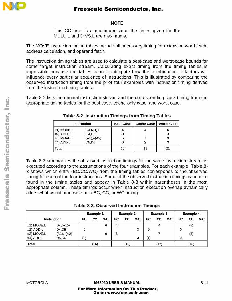
MOTOROLA M68020 USER’S MANUAL 8-11
NOTE
This CC time is a maximum since the times given for theMULU.L and DIVS.L are maximums.
The MOVE instruction timing tables include all necessary timing for extension word fetch,address calculation, and operand fetch.
The instruction timing tables are used to calculate a best-case and worst-case bounds forsome target instruction stream. Calculating exact timing from the timing tables isimpossible because the tables cannot anticipate how the combination of factors willinfluence every particular sequence of instructions. This is illustrated by comparing theobserved instruction timing from the prior four examples with instruction timing derivedfrom the instruction timing tables.
Table 8-2 lists the original instruction stream and the corresponding clock timing from theappropriate timing tables for the best case, cache-only case, and worst case.
Table 8-2. Instruction Timings from Timing Tables
Instruction Best Case Cache Case Worst Case
#1) MOVE.L#2) ADD.L#3) MOVE.L#4) ADD.L
D4,(A1)+D4,D5(A1),–(A2)D5,D6
4060
4272
6393
Total 10 15 21
Table 8-3 summarizes the observed instruction timings for the same instruction stream asexecuted according to the assumptions of the four examples. For each example, Table 8-3 shows which entry (BC/CC/WC) from the timing tables corresponds to the observedtiming for each of the four instructions. Some of the observed instruction timings cannot befound in the timing tables and appear in Table 8-3 within parentheses in the mostappropriate column. These timings occur when instruction execution overlap dynamicallyalters what would otherwise be a BC, CC, or WC timing.
Table 8-3. Observed Instruction Timings
Example 1 Example 2 Example 3 Example 4
Instruction BC CC WC BC CC WC BC CC WC BC CC WC
#1) MOVE.L#2) ADD.L#3) MOVE.L#4) ADD.L
D4,(A1)+D4,D5(A1),–(A2)D5,D6
0
(1)
6
9
4
63
3
0
(1)
4
70
0
(5)
(8)
Total (16) (16) (12) (13)
Fre
esc
ale
Se
mic
on
du
cto
r, I
Freescale Semiconductor, Inc.
For More Information On This Product, Go to: www.freescale.com
nc
...
8-12 M68020 USER’S MANUAL MOTOROLA
Comparing Tables 8-2 and 8-3 demonstrates that calculation of instruction timing cannotbe a simple lookup of only BC or only WC timings. Even when the assumptions are knownand fixed, as in the four examples summarized in Table 8-3, the microprocessor cansometimes achieve best-case timings under worst-case assumptions.
Looking across the four examples in Table 8-3 for an individual instruction, it is difficult topredict which timing table entry is used, since the influence of instruction overlap may ormay not improve the BC, WC, or CC timings. When looking at the observed instructiontimings for one example, it is also difficult to determine which combination of BC/CC/WCtiming is required. Just how the instruction stream will fit and run with the cache enabled,how instructions are positioned in memory, and the degree of instruction overlap arefactors that are impossible to account for in all combinations of the timing tables.
Although the timing tables cannot accurately predict the instruction timing that would beobserved when executing an instruction stream on the MC68020/EC020, the tables canbe used to calculate best-case and worst-case bounds for instruction timing. Absoluteinstruction timing must be measured by using the microprocessor itself to execute thetarget instruction stream.
Fre
esc
ale
Se
mic
on
du
cto
r, I
Freescale Semiconductor, Inc.
For More Information On This Product, Go to: www.freescale.com
nc
...
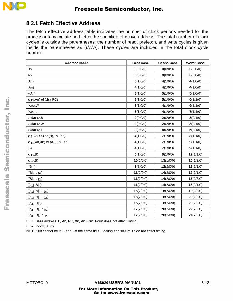
MOTOROLA M68020 USER’S MANUAL 8-13
8.2.1 Fetch Effective Address
The fetch effective address table indicates the number of clock periods needed for theprocessor to calculate and fetch the specified effective address. The total number of clockcycles is outside the parentheses; the number of read, prefetch, and write cycles is giveninside the parentheses as (r/p/w). These cycles are included in the total clock cyclenumber.
Address Mode Best Case Cache Case Worst Case
Dn 0(0/0/0) 0(0/0/0) 0(0/0/0)
An 0(0/0/0) 0(0/0/0) 0(0/0/0)
(An) 3(1/0/0) 4(1/0/0) 4(1/0/0)
(An)+ 4(1/0/0) 4(1/0/0) 4(1/0/0)
–(An) 3(1/0/0) 5(1/0/0) 5(1/0/0)
(d16,An) of (d16,PC) 3(1/0/0) 5(1/0/0) 6(1/1/0)
(xxx).W 3(1/0/0) 4(1/0/0) 6(1/1/0)
(xxx).L 3(1/0/0) 4(1/0/0) 7(1/1/0)
#<data>.B 0(0/0/0) 2(0/0/0) 3(0/1/0)
#<data>.W 0(0/0/0) 2(0/0/0) 3(0/1/0)
#<data>.L 0(0/0/0) 4(0/0/0) 5(0/1/0)
(d8,An,Xn) or (d8,PC,Xn) 4(1/0/0) 7(1/0/0) 8(1/1/0)
(d16,An,Xn) or (d16,PC,Xn) 4(1/0/0) 7(1/0/0) 9(1/1/0)
(B) 4(1/0/0) 7(1/0/0) 9(1/1/0)
(d16,B) 6(1/0/0) 9(1/0/0) 12(1/1/0)
(d32,B) 10(1/0/0) 13(1/0/0) 16(1/2/0)
([B],I) 9(2/0/0) 12(2/0/0) 13(2/1/0)
([B],I,d16) 11(2/0/0) 14(2/0/0) 16(2/1/0)
([B],I,d32) 11(2/0/0) 14(2/0/0) 17(2/2/0)
([d16,B],I) 11(2/0/0) 14(2/0/0) 16(2/1/0)
([d16,B],I,d16) 13(2/0/0) 16(2/0/0) 19(2/2/0)
([d16,B],I,d32) 13(2/0/0) 16(2/0/0) 20(2/2/0)
([d32,B],I) 15(2/0/0) 18(2/0/0) 20(2/2/0)
([d32,B],I,d16) 17(2/0/0) 20(2/0/0) 22(2/2/0)
([d32,B],I,d32) 17(2/0/0) 20(2/0/0) 24(2/3/0)
B = Base address; 0, An, PC, Xn, An + Xn. Form does not affect timing.I = Index; 0, XnNOTE: Xn cannot be in B and I at the same time. Scaling and size of Xn do not affect timing.
Fre
esc
ale
Se
mic
on
du
cto
r, I
Freescale Semiconductor, Inc.
For More Information On This Product, Go to: www.freescale.com
nc
...

8-14 M68020 USER’S MANUAL MOTOROLA
8.2.2 Fetch Immediate Effective Address
The fetch immediate effective address table indicates the number of clock periods neededfor the processor to fetch the immediate source operand and calculate and fetch thespecified destination operand. The total number of clock cycles is outside theparentheses; the number of read, prefetch, and write cycles is given inside theparentheses as (r/p/w). These cycles are included in the total clock cycle number.
Address Mode Best Case Cache Case Worst Case
#<data>.W,Dn 0(0/0/0) 2(0/0/0) 3(0/1/0)
#<data>.L,Dn 1(0/0/0) 4(0/0/0) 5(0/1/0)
#<data>.W,(An) 3(1/0/0) 4(1/0/0) 4(1/1/0)
#<data>.L,(An) 3(1/0/0) 4(1/0/0) 7(1/1/0)
#<data>.W,(An)+ 4(1/0/0) 6(1/0/0) 7(1/1/0)
#<data>.L,(An)+ 5(1/0/0) 8(1/0/0) 9(1/1/0)
#<data>.W,–(An) 3(1/0/0) 5(1/0/0) 6(1/1/0)
#<data>.L,–(An) 4(1/0/0) 7(1/0/0) 8(1/1/0)
#<data>.W,(bd,An) 3(1/0/0) 5(1/0/0) 7(1/1/0)
#<data>.L,(bd,An) 4(1/0/0) 7(1/0/0) 10(1/2/0)
#<data>.W,xxx.W 3(1/0/0) 5(1/0/0) 7(1/1/0)
#<data>.L,xxx.W 4(1/0/0) 7(1/0/0) 10(1/2/0)
#<data>.W,xxx.L 3(1/0/0) 6(1/0/0) 10(1/2/0)
#<data>.L,xxx.L 4(1/0/0) 8(1/0/0) 12(1/2/0)
#<data>.W,#<data>.B,W 0(0/0/0) 4(0/0/0) 6(0/2/0)
#<data>.L,#<data>.B,W 1(0/0/0) 6(0/0/0) 8(0/2/0)
#<data>.W,#<data>.L 0(0/0/0) 6(0/0/0) 8(0/2/0)
#<data>.L,#(data>.L 1(0/0/0) 8(0/0/0) 10(0/2/0)
#<data>.W,(d8,An,Xn) or (d8,PC,Xn) 4(1/0/0) 9(1/0/0) 11(1/2/0)
#<data>.L,(d8,An,Xn) or (d8,PC,Xn) 5(1/0/0) 11(1/0/0) 13(1/2/0)
#<data>.W,(d16,An,Xn) or (d16,PC,Xn) 4(1/0/0) 9(1/0/0) 12(1/2/0)
#<data>.L,(d16,An,Xn) or (d16,PC,Xn) 5(1/0/0) 11(1/0/0) 15(1/2/0)
#<data>.W,(B) 4(1/0/0) 9(1/0/0) 12(1/1/0)
#<data>.L,(B) 5(1/0/0) 11(1/0/0) 14(1/2/0)
#<data>.W,(bd,PC) 10(1/0/0) 15(1/0/0) 19(1/3/0)
#<data>.L,(bd,PC) 11(1/0/0) 17(1/0/0) 21(1/3/0)
#<data>.W,(d16,B) 6(1/0/0) 11(1/0/0) 15(1/2/0)
#<data>.L,(d16,B) 7(1/0/0) 13(1/0/0) 17(1/2/0)
#<data>.W,(d32,B) 10(1/0/0) 15(1/0/0) 19(1/3/0)
#<data>.L,(d32,B) 11(1/0/0) 17(1/0/0) 21(1/3/0)
#<data>.W,([B],I) 9(2/0/0) 14(2/0/0) 16(2/2/0)
#<data>.L,([B],I) 10(2/0/0) 16(2/0/0) 18(2/2/0)
#<data>.W,([B],I,d16) 11(2/0/0) 16(2/0/0) 19(2/2/0)
#<data>.L,([B],I,d16) 12(2/0/0) 18(2/0/0) 21(2/2/0)
Fre
esc
ale
Se
mic
on
du
cto
r, I
Freescale Semiconductor, Inc.
For More Information On This Product, Go to: www.freescale.com
nc
...
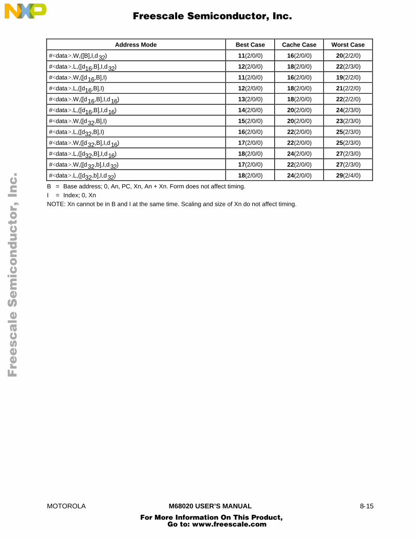
MOTOROLA M68020 USER’S MANUAL 8-15
Address Mode Best Case Cache Case Worst Case
#<data>.W,([B],I,d32) 11(2/0/0) 16(2/0/0) 20(2/2/0)
#<data>.L,([d16,B],I,d32) 12(2/0/0) 18(2/0/0) 22(2/3/0)
#<data>.W,([d16,B],I) 11(2/0/0) 16(2/0/0) 19(2/2/0)
#<data>.L,([d16,B],I) 12(2/0/0) 18(2/0/0) 21(2/2/0)
#<data>.W,([d16,B],I,d16) 13(2/0/0) 18(2/0/0) 22(2/2/0)
#<data>.L,([d16,B],I,d16) 14(2/0/0) 20(2/0/0) 24(2/3/0)
#<data>.W,([d32,B],I) 15(2/0/0) 20(2/0/0) 23(2/3/0)
#<data>.L,([d32,B],I) 16(2/0/0) 22(2/0/0) 25(2/3/0)
#<data>.W,([d32,B],I,d16) 17(2/0/0) 22(2/0/0) 25(2/3/0)
#<data>.L,([d32,B],I,d16) 18(2/0/0) 24(2/0/0) 27(2/3/0)
#<data>.W,([d32,b],I,d32) 17(2/0/0) 22(2/0/0) 27(2/3/0)
#<data>.L,([d32,b],I,d32) 18(2/0/0) 24(2/0/0) 29(2/4/0)
B = Base address; 0, An, PC, Xn, An + Xn. Form does not affect timing.I = Index; 0, XnNOTE: Xn cannot be in B and I at the same time. Scaling and size of Xn do not affect timing.
Fre
esc
ale
Se
mic
on
du
cto
r, I
Freescale Semiconductor, Inc.
For More Information On This Product, Go to: www.freescale.com
nc
...

8-16 M68020 USER’S MANUAL MOTOROLA
8.2.3 Calculate Effective Address
The calculate immediate effective address table indicates the number of clock periodsneeded for the processor to calculate the specified effective address. Fetch time is onlyincluded for the first level of indirection on memory indirect addressing modes. The totalnumber of clock cycles is outside the parentheses; the number of read, prefetch, and writecycles is given inside the parentheses as (r/p/w). These cycles are included in the totalclock cycle number.
Address Mode Best Case Cache Case Worst Case
Dn 0(0/0/0) 0(0/0/0) 0(0/0/0)
An 0(0/0/0) 0(0/0/0) 0(0/0/0)
(An) 2(0/0/0) 2(0/0/0) 2(0/0/0)
(An)+ 2(0/0/0) 2(0/0/0) 2(0/0/0)
–(An) 2(0/0/0) 2(0/0/0) 2(0/0/0)
(d16,An) or (d16,PC) 2(0/0/0) 2(0/0/0) 3(0/1/0)
<data>.W 2(0/0/0) 2(0/0/0) 3(0/1/0)
<data>.L 1(0/0/0) 4(0/0/0) 5(0/1/0)
(d8,An,Xn) or (d8,PC,Xn) 1(0/0/0) 4(0/0/0) 5(0/1/0)
(d16,An,Xn) or (d16,PC,Xn) 3(0/0/0) 6(0/0/0) 7(0/1/0)
(B) 3(0/0/0) 6(0/0/0) 7(0/1/0)
(d16,B) 5(0/0/0) 8(0/0/0) 10(0/1/0)
(d32,B) 9(0/0/0) 12(0/0/0) 15(0/2/0)
([B],I) 8(1/0/0) 11(1/0/0) 12(1/1/0)
([B],I,d16) 10(1/0/0) 13(1/0/0) 15(1/1/0)
([B],I,d32) 10(1/0/0) 13(1/0/0) 16(1/2/0)
([d16,B],I) 10(1/0/0) 13(1/0/0) 15(1/1/0)
([d16,B],I,d16) 12(1/0/0) 15(1/0/0) 18(1/2/0)
([d16,B],I,d32) 12(1/0/0) 15(1/0/0) 19(1/2/0)
([d32,B],I) 14(1/0/0) 17(1/0/0) 19(1/2/0)
([d32,B],I,d16) 16(1/0/0) 19(1/0/0) 21(1/2/0)
([d32,B],I,d32) 16(1/0/0) 19(1/0/0) 24(1/3/0)
B = Base address; 0, An, PC, Xn, An + Xn. Form does not affect timing.I = Index; 0, XnNOTE: Xn cannot be in B and I at the same time. Scaling and size of Xn do not affect timing.
Fre
esc
ale
Se
mic
on
du
cto
r, I
Freescale Semiconductor, Inc.
For More Information On This Product, Go to: www.freescale.com
nc
...

MOTOROLA M68020 USER’S MANUAL 8-17
8.2.4 Calculate Immediate Effective Address
The calculate immediate effective address table indicates the number of clock periodsneeded for the processor to fetch the immediate source operand and calculate thespecified destination effective address. Fetch time is only included for the first level ofindirection on memory indirect addressing modes. The total number of clock cycles isoutside the parentheses; the number of read, prefetch, and write cycles is given inside theparentheses as (r/p/w). These cycles are included in the total clock cycle number.
Address Mode Best Case Cache Case Worst Case
#<data>.W,Dn 0(0/0/0) 2(0/0/0) 3(0/1/0)
#<data>.L,Dn 1(0/0/0) 4(0/0/0) 5(0/1/0)
#<data>.W,(An) 0(0/0/0) 2(0/0/0) 3(0/1/0)
#<data>.L,(An) 1(0/0/0) 4(0/0/0) 5(0/1/0)
#<data>.W,(An)+ 2(0/0/0) 4(0/0/0) 5(0/1/0)
#<data>.L,(An)+ 3(0/0/0) 6(0/0/0) 7(0/1/0)
#<data>.W,(bd,An) 1(0/0/0) 4(0/0/0) 5(0/1/0)
#<data>.L,(bd,An) 3(0/0/0) 6(0/0/0) 8(0/2/0)
#<data>.W,xxx.W 1(0/0/0) 4(0/0/0) 5(0/1/0)
#<data>.L,xxx.W 3(0/0/0) 6(0/0/0) 8(0/2/0)
#<data>.W,xxx.L 2(0/0/0) 4(0/0/0) 6(0/2/0)
#<data>.L,xxx.L 3(0/0/0) 8(0/0/0) 10(0/2/0)
#<data>.W,(d8,An,Xn) or (d8,PC,Xn) 0(0/0/0) 6(0/0/0) 8(0/2/0)
#<data>.L,(d8,An,Xn) or (d8,PC,Xn) 2(0/0/0) 8(0/0/0) 10(0/2/0)
#<data>.W,(d16,An,Xn) or (d16,PC,Xn) 3(0/0/0) 8(0/0/0) 10(0/2/0)
#<data>.L,(d16,An,Xn) or (d16,PC,Xn) 4(0/0/0) 10(0/0/0) 12(0/2/0)
#<data>.W,(B) 3(0/0/0) 8(0/0/0) 10(0/1/0)
#<data>.L,(B) 4(0/0/0) 10(0/0/0) 12(0/2/0)
#<data>.W,(bd,PC) 9(0/0/0) 14(0/0/0) 18(0/3/0)
#<data>.L,(bd,PC) 10(0/0/0) 16(0/0/0) 20(0/3/0)
#<data>.W,(d16,B) 5(0/0/0) 10(0/0/0) 13(0/2/0)
#<data>.L,(d16,B) 6(0/0/0) 12(0/0/0) 15(0/2/0)
#<data>.W,(d32,B) 9(0/0/0) 14(0/0/0) 18(0/2/0)
#<data>.L,(d32,B) 10(0/0/0) 16(0/0/0) 20(0/3/0)
#<data>.W,([B],I) 8(1/0/0) 13(1/0/0) 15(1/2/0)
#<data>.L,([B],I) 9(1/0/0) 15(1/0/0) 17(1/2/0)
#<data>.W,([B],I,d16) 10(1/0/0) 15(1/0/0) 18(1/2/0)
#<data>.L,([B],I,d16) 11(1/0/0) 17(1/0/0) 20(1/2/0)
#<data>.W,([B],I,d32) 10(1/0/0) 15(1/0/0) 19(1/2/0)
#<data>.L,([d16,B],I,d32) 11(1/0/0) 17(1/0/0) 21(1/3/0)
#<data>.W,([d16,B],I) 10(1/0/0) 15(1/0/0) 18(1/2/0)
#<data>.L,([d16,B],I) 11(1/0/0) 17(1/0/0) 20(1/2/0)
#<data>.W,([d16,B],I,d16) 12(1/0/0) 17(1/0/0) 21(1/2/0)
Fre
esc
ale
Se
mic
on
du
cto
r, I
Freescale Semiconductor, Inc.
For More Information On This Product, Go to: www.freescale.com
nc
...

8-18 M68020 USER’S MANUAL MOTOROLA
Address Mode Best Case Cache Case Worst Case
#<data>.L,([d16,B],I,d16) 13(1/0/0) 19(1/0/0) 23(1/3/0)
#<data>.([d16,B],I,d32) 12(1/0/0) 17(1/0/0) 22(1/3/0)
#<data>.([d16,B],I,d32) 13(1/0/0) 19(1/0/0) 24(1/3/0)
#<data>.W,([d32,B],I) 14(1/0/0) 19(1/0/0) 22(1/3/0)
#<data>.L,([d32,B],I) 15(1/0/0) 21(1/0/0) 24(1/3/0)
#<data>.W,([d32,B],I,d16) 16(1/0/0) 21(1/0/0) 24(1/3/0)
#<data>.L,([d32,B],I,d16) 17(1/0/0) 23(1/0/0) 26(1/3/0)
#<data>.W,([d32,B],I,d32) 16(1/0/0) 21(1/0/0) 24(1/3/0)
#<data>.L,([d32,B],I,d32) 17(1/0/0) 23(1/0/0) 29(1/4/0)
B = Base address; 0, An, PC, Xn, An + Xn. Form does not affect timing.I = Index; 0, XnNOTE: Xn cannot be in B and I at the same time. Scaling and size of Xn do not affect timing.
Fre
esc
ale
Se
mic
on
du
cto
r, I
Freescale Semiconductor, Inc.
For More Information On This Product, Go to: www.freescale.com
nc
...

MOTOROLA M68020 USER’S MANUAL 8-19
8.2.5 Jump Effective Address
The jump effective address table indicates the number of clock periods needed for theprocessor to calculate the specified effective address. Fetch time is only included for thefirst level of indirection on memory indirect addressing modes. The total number of clockcycles is outside the parentheses; the number or read, prefetch, and write cycles is giveninside the parentheses as (r/p/w). These cycles are included in the total clock cyclenumber.
Address Mode Best Case Cache Case Worst Case
(An) 0(0/0/0) 2(0/0/0) 2(0/0/0)
(d16,An) 1(0/0/0) 4(0/0/0) 4(0/0/0)
(xxx).W 0(0/0/0) 2(0/0/0) 2(0/0/0)
(xxx).L 0(0/0/0) 2(0/0/0) 2(0/0/0)
(d8,An,Xn) or (d8,PC,Xn) 3(0/0/0) 6(0/0/0) 6(0/0/0)
(d16,An,Xn) or (d16,PC,Xn) 3(0/0/0) 6(0/0/0) 6(0/0/0)
(B) 3(0/0/0) 6(0/0/0) 6(0/0/0)
(B,d16) 5(0/0/0) 8(0/0/0) 8(0/1/0)
(B,d32) 9(0/0/0) 12(0/0/0) 12(0/1/0)
([B],I) 8(1/0/0) 11(1/0/0) 11(1/1/0)
([B],I,d16) 10(1/0/0) 13(1/0/0) 14(1/1/0)
([B],I,d32) 10(1/0/0) 13(1/0/0) 14(1/1/0)
([d16,B],I) 10(1/0/0) 13(1/0/0) 14(1/1/0)
([d16,B],I,d16) 12(1/0/0) 15(1/0/0) 17(1/1/0)
([d16,B],I,d32) 12(1/0/0) 15(1/0/0) 17(1/1/0)
([d32,B],I) 14(1/0/0) 17(1/0/0) 19(1/2/0)
([d32,B],I,d16) 16(1/0/0) 19(1/0/0) 21(1/2/0)
([d32,B],I,d32) 16(1/0/0) 19(1/0/0) 23(1/2/0)
B = Base address; 0, An, PC, Xn, An + Xn, PC + Xn. Form does not affect timing.I = Index; 0, XnNOTE: Xn cannot be in B and I at the same time. Scaling and size of Xn do not affect timing.
Fre
esc
ale
Se
mic
on
du
cto
r, I
Freescale Semiconductor, Inc.
For More Information On This Product, Go to: www.freescale.com
nc
...

8-20 M68020 USER’S MANUAL MOTOROLA
8.2.6 MOVE Instruction
The MOVE instruction table indicates the number of clock periods needed for theprocessor to fetch, calculate, and perform the MOVE or MOVEA with the specified sourceand destination effective addresses, including both levels of indirection on memory indirectaddressing modes. No additional tables are needed to calculate the total effectiveexecution time for the MOVE or MOVEA instruction. The total number of clock cycles isoutside the parentheses; the number of read, prefetch, and write cycles is given inside theparentheses as (r/p/w). These cycles are included in the total clock cycle number.
BEST CASE
Destination
Source Address Mode An Dn (An) (An)+ –(An) (d16,An) (xxx).W (xxx).L
Rn 0(0/0/0) 0(0/0/0) 3(0/0/1) 4(0/0/1) 3(0/0/1) 3(0/0/1) 3(0/0/1) 5(0/0/1)
#<data>.B,W 0(0/0/0) 0(0/0/0) 3(0/0/1) 4(0/0/1) 3(0/0/1) 3(0/0/1) 3(0/0/1) 5(0/0/1)
#<data>.L 0(0/0/0) 0(0/0/0) 3(0/0/1) 4(0/0/1) 3(0/0/1) 3(0/0/1) 3(0/0/1) 5(0/0/1)
(An) 3(1/0/0) 3(1/0/0) 6(1/0/1) 6(1/0/1) 6(1/0/1) 6(1/0/1) 6(1/0/1) 8(1/0/1)
(An)+ 4(1/0/0) 4(1/0/0) 7(1/0/1) 7(1/0/1) 7(1/0/1) 7(1/0/1) 7(1/0/1) 9(1/0/1)
–(An) 3(1/0/0) 3(1/0/0) 6(1/0/1) 6(1/0/1) 6(1/0/1) 6(1/0/1) 6(1/0/1) 8(1/0/1)
(d16,An) or (d16,PC) 3(1/0/0) 3(1/0/0) 6(1/0/1) 6(1/0/1) 6(1/0/1) 6(1/0/1) 6(1/0/1) 8(1/0/1)
(xxx).W 3(1/0/0) 3(1/0/0) 6(1/0/1) 6(1/0/1) 6(1/0/1) 6(1/0/1) 6(1/0/1) 8(1/0/1)
(xxx).L 3(1/0/0) 3(1/0/0) 6(1/0/1) 6(1/0/1) 6(1/0/1) 6(1/0/1) 6(1/0/1) 8(1/0/1)
(d8,An,Xn) or (d8,PC,Xn) 4(1/0/0) 4(1/0/0) 7(1/0/1) 7(1/0/1) 7(1/0/1) 7(1/0/1) 7(1/0/1) 9(1/0/1)
(d16,An,Xn) or (d16,PC,Xn) 4(1/0/0) 4(1/0/0) 7(1/0/1) 7(1/0/1) 7(1/0/1) 7(1/0/1) 7(1/0/1) 9(1/0/1)
(B) 4(1/0/0) 4(1/0/0) 7(1/0/1) 7(1/0/1) 7(1/0/1) 7(1/0/1) 7(1/0/1) 9(1/0/1)
(d16,B) 6(1/0/0) 6(1/0/0) 9(1/0/1) 9(1/0/1) 9(1/0/1) 9(1/0/1) 9(1/0/1) 11(1/0/1)
(d32,B) 10(1/0/0) 10(1/0/0) 13(1/0/1) 13(1/0/1) 13(1/0/1) 13(1/0/1) 13(1/0/1) 15(1/0/1)
([B],I) 9(2/0/0) 9(2/0/0) 12(2/0/1) 12(2/0/1) 12(2/0/1) 12(2/0/1) 12(2/0/1) 14(2/0/1)
([B],I,d16) 11(2/0/0) 11(2/0/0) 14(2/0/1) 14(2/0/1) 14(2/0/1) 14(2/0/1) 14(2/0/1) 16(2/0/1)
([B],I,d32) 11(2/0/0) 11(2/0/0) 14(2/0/1) 14(2/0/1) 14(2/0/1) 14(2/0/1) 14(2/0/1) 16(2/0/1)
([d16,B],I) 11(2/0/0) 11(2/0/0) 14(2/0/1) 14(2/0/1) 14(2/0/1) 14(2/0/1) 14(2/0/1) 16(2/0/1)
([d16,B],I,d16) 13(2/0/0) 13(2/0/0) 16(2/0/1) 16(2/0/1) 16(2/0/1) 16(2/0/1) 16(2/0/1) 18(2/0/1)
([d16,B],d32) 13(2/0/0) 13(2/0/0) 16(2/0/1) 16(2/0/1) 16(2/0/1) 16(2/0/1) 16(2/0/1) 18(2/0/1)
([d32,B],I) 15(2/0/0) 15(2/0/0) 18(2/0/1) 18(2/0/1) 18(2/0/1) 18(2/0/1) 18(2/0/1) 20(2/0/1)
([d32,B],I,d16) 17(2/0/0) 17(2/0/0) 20(2/0/1) 20(2/0/1) 20(2/0/1) 20(2/0/1) 20(2/0/1) 22(2/0/1)
([d32,B],I,d32) 17(2/0/0) 17(2/0/0) 20(2/0/1) 20(2/0/1) 20(2/0/1) 20(2/0/1) 20(2/0/1) 22(2/0/1)
Fre
esc
ale
Se
mic
on
du
cto
r, I
Freescale Semiconductor, Inc.
For More Information On This Product, Go to: www.freescale.com
nc
...

MOTOROLA M68020 USER’S MANUAL 8-21
BEST CASE (Continued)
Source Destination
Address Mode (d8,An,Xn) (d16,An,Xn) (B) (d16,B) (d32,B) ([B],I) ([B],I,d16) ([B],I,d32)
Rn 4(0/0/1) 6(0/0/1) 5(0/0/1) 7(0/0/1) 11(0/0/1) 9(1/0/1) 11(1/0/1) 12(1/0/1)
#<data>.B,W 4(0/0/1) 6(0/0/1) 5(0/0/1) 7(0/0/1) 11(0/0/1) 9(1/0/1) 11(1/0/1) 12(1/0/1)
#<data>.L 4(0/0/1) 6(0/0/1) 5(0/0/1) 7(0/0/1) 11(0/0/1) 9(1/0/1) 11(1/0/1) 12(1/0/1)
(An) 8(1/0/1) 10(1/0/1) 9(1/0/1) 11(1/0/1) 15(1/0/1) 13(2/0/1) 15(2/0/1) 16(2/0/1)
(An)+ 9(1/0/1) 11(1/0/1) 10(1/0/1) 12(1/0/1) 16(1/0/1) 14(2/0/1) 16(2/0/1) 17(2/0/1)
–(An) 8(1/0/1) 10(1/0/1) 9(1/0/1) 11(1/0/1) 15(1/0/1) 13(2/0/1) 15(2/0/1) 16(2/0/1)
(d16,An) or(d16,PC)
8(1/0/1) 10(1/0/1) 9(1/0/1) 11(1/0/1) 15(1/0/1) 13(2/0/1) 15(2/0/1) 16(2/0/1)
(xxx).W 8(1/0/1) 10(1/0/1) 9(1/0/1) 11(1/0/1) 15(1/0/1) 13(2/0/1) 15(2/0/1) 16(2/0/1)
(xxx).L 8(1/0/1) 10(1/0/1) 9(1/0/1) 11(1/0/1) 15(1/0/1) 13(2/0/1) 15(2/0/1) 16(2/0/1)
(d8,An,Xn) or(d8,PC,Xn)
9(1/0/1) 10(1/0/1) 10(1/0/1) 12(1/0/1) 16(1/0/1) 14(2/0/1) 16(2/0/1) 17(2/0/1)
(d16,An,Xn) or(d16,PC,Xn)
9(1/0/1) 11(1/0/1) 10(1/0/1) 12(1/0/1) 16(1/0/1) 14(2/0/1) 16(2/0/1) 17(2/0/1)
(B) 9(1/0/1) 11(1/0/1) 10(1/0/1) 12(1/0/1) 16(1/0/1) 14(2/0/1) 16(2/0/1) 17(2/0/1)
(d16,B) 11(1/0/1) 13(1/0/1) 12(1/0/1) 14(1/0/1) 18(1/0/1) 16(2/0/1) 18(2/0/1) 19(2/0/1)
(d32,B) 15(1/0/1) 17(1/0/1) 18(1/0/1) 18(1/0/1) 22(1/0/1) 20(2/0/1) 22(2/0/1) 23(2/0/1)
([B],I) 14(2/0/1) 16(2/0/1) 17(2/0/1) 17(2/0/1) 21(2/0/1) 19(3/0/1) 21(3/0/1) 22(3/0/1)
([B],I,d16) 16(2/0/1) 18(2/0/1) 19(2/0/1) 19(2/0/1) 23(2/0/1) 21(3/0/1) 23(3/0/1) 24(3/0/1)
([B],I,d32) 16(2/0/1) 18(2/0/1) 19(2/0/1) 19(2/0/1) 23(2/0/1) 21(3/0/1) 23(3/0/1) 24(3/0/1)
([d16,B],I) 16(2/0/1) 18(2/0/1) 19(2/0/1) 19(2/0/1) 23(2/0/1) 21(3/0/1) 23(3/0/1) 24(3/0/1)
([d16,B],I,d16) 18(2/0/1) 20(2/0/1) 21(2/0/1) 21(2/0/1) 25(2/0/1) 23(3/0/1) 25(3/0/1) 26(3/0/1)
([d16,B],I,d32) 18(2/0/1) 20(2/0/1) 21(2/0/1) 21(2/0/1) 25(2/0/1) 23(3/0/1) 25(3/0/1) 26(3/0/1)
([d32,B],I) 20(2/0/1) 22(2/0/1) 23(2/0/1) 23(2/0/1) 27(2/0/1) 25(3/0/1) 27(3/0/1) 28(3/0/1)
([d32,B],I,d16) 22(2/0/1) 24(2/0/1) 25(2/0/1) 25(2/0/1) 29(2/0/1) 27(3/0/1) 29(3/0/1) 30(3/0/1)
([d32,B],I,d32) 22(2/0/1) 24(2/0/1) 25(2/0/1) 25(2/0/1) 29(2/0/1) 27(3/0/1) 29(3/0/1) 30(3/0/1)
Fre
esc
ale
Se
mic
on
du
cto
r, I
Freescale Semiconductor, Inc.
For More Information On This Product, Go to: www.freescale.com
nc
...

8-22 M68020 USER’S MANUAL MOTOROLA
BEST CASE (Concluded)
Source Destination
Address Mode ([d16,B],I) ([d16,B],I,d16) ([d16,B],I,d32) ([d32,B],I) ([d32,B],I,d16) ([d32,B],I,d32)
Rn 11(1/0/1) 13(1/0/1) 14(1/0/1) 15(1/0/1) 17(1/0/1) 18(1/0/1)
#<data>.B,W 11(1/0/1) 13(1/0/1) 14(1/0/1) 15(1/0/1) 17(1/0/1) 18(1/0/1)
#<data>.L 11(1/0/1) 13(1/0/1) 14(1/0/1) 15(1/0/1) 17(1/0/1) 18(1/0/1)
(An) 15(2/0/1) 17(2/0/1) 18(2/0/1) 19(2/0/1) 21(2/0/1) 22(2/0/1)
(An)+ 16(2/0/1) 18(2/0/1) 19(2/0/1) 20(2/0/1) 22(2/0/1) 23(2/0/1)
–(An) 15(2/0/1) 17(2/0/1) 18(2/0/1) 19(2/0/1) 21(2/0/1) 22(2/0/1)
(d16,An) or (d16,PC) 15(2/0/1) 17(2/0/1) 18(2/0/1) 19(2/0/1) 21(2/0/1) 22(2/0/1)
(xxx).W 15(2/0/1) 17(2/0/1) 18(2/0/1) 19(2/0/1) 21(2/0/1) 22(2/0/1)
(xxx).L 15(2/0/1) 17(2/0/1) 18(2/0/1) 19(2/0/1) 21(2/0/1) 22(2/0/1)
(d8,An,Xn) or(d8,PC,Xn)
16(2/0/1) 18(2/0/1) 19(2/0/1) 20(2/0/1) 22(2/0/1) 23(2/0/1)
(d16,An,Xn) or(d16,PC,Xn)
16(2/0/1) 18(2/0/1) 19(2/0/1) 20(2/0/1) 22(2/0/1) 23(2/0/1)
(B) 16(2/0/1) 18(2/0/1) 19(2/0/1) 20(2/0/1) 22(2/0/1) 23(2/0/1)
(d16,B) 18(2/0/1) 20(2/0/1) 21(2/0/1) 22(2/0/1) 24(2/0/1) 25(2/0/1)
(d32,B) 22(2/0/1) 24(2/0/1) 25(2/0/1) 26(2/0/1) 28(2/0/1) 29(2/0/1)
([B],I) 21(3/0/1) 23(3/0/1) 24(3/0/1) 25(3/0/1) 27(3/0/1) 28(3/0/1)
([B],I,d16) 23(3/0/1) 25(3/0/1) 26(3/0/1) 27(3/0/1) 29(3/0/1) 30(3/0/1)
([B],I,d32) 23(3/0/1) 25(3/0/1) 26(3/0/1) 27(3/0/1) 29(3/0/1) 30(3/0/1)
([d16,B],I) 23(3/0/1) 25(3/0/1) 26(3/0/1) 27(3/0/1) 29(3/0/1) 30(3/0/1)
([d16,B],I,d16) 25(3/0/1) 27(3/0/1) 28(3/0/1) 29(3/0/1) 31(3/0/1) 32(3/0/1)
([d16,B],I,d32) 25(3/0/1) 27(3/0/1) 28(3/0/1) 29(3/0/1) 31(3/0/1) 32(0/0/1)
([d32,B],I) 27(3/0/1) 29(3/0/1) 30(3/0/1) 31(3/0/1) 33(3/0/1) 34(3/0/1)
([d32,B],I,d16) 29(3/0/1) 31(3/0/1) 32(3/0/1) 33(3/0/1) 35(3/0/1) 36(3/0/1)
([d32,B],I,d32) 29(3/0/1) 31(3/0/1) 32(3/0/1) 33(3/0/1) 35(3/0/1) 36(3/0/1)
Fre
esc
ale
Se
mic
on
du
cto
r, I
Freescale Semiconductor, Inc.
For More Information On This Product, Go to: www.freescale.com
nc
...

MOTOROLA M68020 USER’S MANUAL 8-23
CACHE CASE
Source Destination
Address Mode An Dn (An) (An)+ –(An) (d16,An) (xxx).W (xxx).L
Rn 2(0/0/0) 2(0/0/0) 4(0/0/1) 4(0/0/1) 5(0/0/1) 5(0/0/1) 4(0/0/1) 6(0/0/1)
#<data>.B,W 4(0/0/0) 4(0/0/0) 6(0/0/1) 6(0/0/1) 7(0/0/1) 7(0/0/1) 6(0/0/1) 8(0/0/1)
#<data>.L 6(0/0/0) 6(0/0/0) 8(0/0/1) 8(0/0/1) 9(0/0/1) 9(0/0/1) 8(0/0/1) 10(0/0/1)
(An) 6(1/0/0) 6(1/0/0) 7(1/0/1) 7(1/0/1) 7(1/0/1) 7(1/0/1) 7(1/0/1) 9(1/0/1)
(An)+ 6(1/0/0) 6(1/0/0) 7(1/0/1) 7(1/0/1) 7(1/0/1) 7(1/0/1) 7(1/0/1) 9(1/0/1)
–(An) 7(1/0/0) 7(1/0/0) 8(1/0/1) 8(1/0/1) 8(1/0/1) 8(1/0/1) 8(1/0/1) 10(1/0/1)
(d16,An) or(d16,PC)
7(1/0/0) 7(1/0/0) 8(1/0/1) 8(1/0/1) 8(1/0/1) 8(1/0/1) 8(1/0/1) 10(1/0/1)
(xxx).W 6(1/0/0) 6(1/0/0) 7(1/0/1) 7(1/0/1) 7(1/0/1) 7(1/0/1) 7(1/0/1) 9(1/0/1)
(xxx).L 6(1/0/0) 6(1/0/0) 7(1/0/1) 7(1/0/1) 7(1/0/1) 7(1/0/1) 7(1/0/1) 9(1/0/1)
(d8,An,Xn) or(d8,PC,Xn)
9(1/0/0) 9(1/0/0) 10(1/0/1) 10(1/0/1) 10(1/0/1) 10(1/0/1) 10(1/0/1) 12(1/0/1)
(d16,An,Xn) or(d16,PC,Xn)
9(1/0/0) 9(1/0/0) 10(1/0/1) 10(1/0/1) 10(1/0/1) 10(1/0/1) 10(1/0/1) 12(1/0/1)
(B) 9(1/0/0) 9(1/0/0) 10(1/0/1) 10(1/0/1) 10(1/0/1) 10(1/0/1) 10(1/0/1) 12(1/0/1)
(d16,B) 11(1/0/0) 11(1/0/0) 12(1/0/1) 12(1/0/1) 12(1/0/1) 12(1/0/1) 12(1/0/1) 14(1/0/1)
(d32,B) 15(1/0/0) 15(1/0/0) 16(1/0/1) 16(1/0/1) 16(1/0/1) 16(1/0/1) 16(1/0/1) 18(1/0/1)
([B],I) 14(2/0/0) 14(2/0/0) 15(2/0/1) 15(2/0/1) 15(2/0/1) 15(2/0/1) 15(2/0/1) 17(2/0/1)
([B],I,d16) 16(2/0/0) 16(2/0/0) 17(2/0/1) 17(2/0/1) 17(2/0/1) 17(2/0/1) 17(2/0/1) 19(2/0/1)
([B],I,d32) 16(2/0/0) 16(2/0/0) 17(2/0/1) 17(2/0/1) 17(2/0/1) 17(2/0/1) 17(2/0/1) 19(2/0/1)
([d16,B],I) 16(2/0/0) 16(2/0/0) 17(2/0/1) 17(2/0/1) 17(2/0/1) 17(2/0/1) 17(2/0/1) 19(2/0/1)
([d16,B],I,d16) 18(2/0/0) 18(2/0/0) 19(2/0/1) 19(2/0/1) 19(2/0/1) 19(2/0/1) 19(2/0/1) 21(2/0/1)
([d16,B],d32) 18(2/0/0) 18(2/0/0) 19(2/0/1) 19(2/0/1) 19(2/0/1) 19(2/0/1) 19(2/0/1) 21(2/0/1)
([d32,B],I) 20(2/0/0) 20(2/0/0) 21(2/0/1) 21(2/0/1) 21(2/0/1) 21(2/0/1) 21(2/0/1) 23(2/0/1)
([d32,B],I,d16) 22(2/0/0) 22(2/0/0) 23(2/0/1) 23(2/0/1) 23(2/0/1) 23(2/0/1) 23(2/0/1) 25(2/0/1)
([d32,B],I,d32) 22(2/0/0) 22(2/0/0) 23(2/0/1) 23(2/0/1) 23(2/0/1) 23(2/0/1) 23(2/0/1) 25(2/0/1)
Fre
esc
ale
Se
mic
on
du
cto
r, I
Freescale Semiconductor, Inc.
For More Information On This Product, Go to: www.freescale.com
nc
...
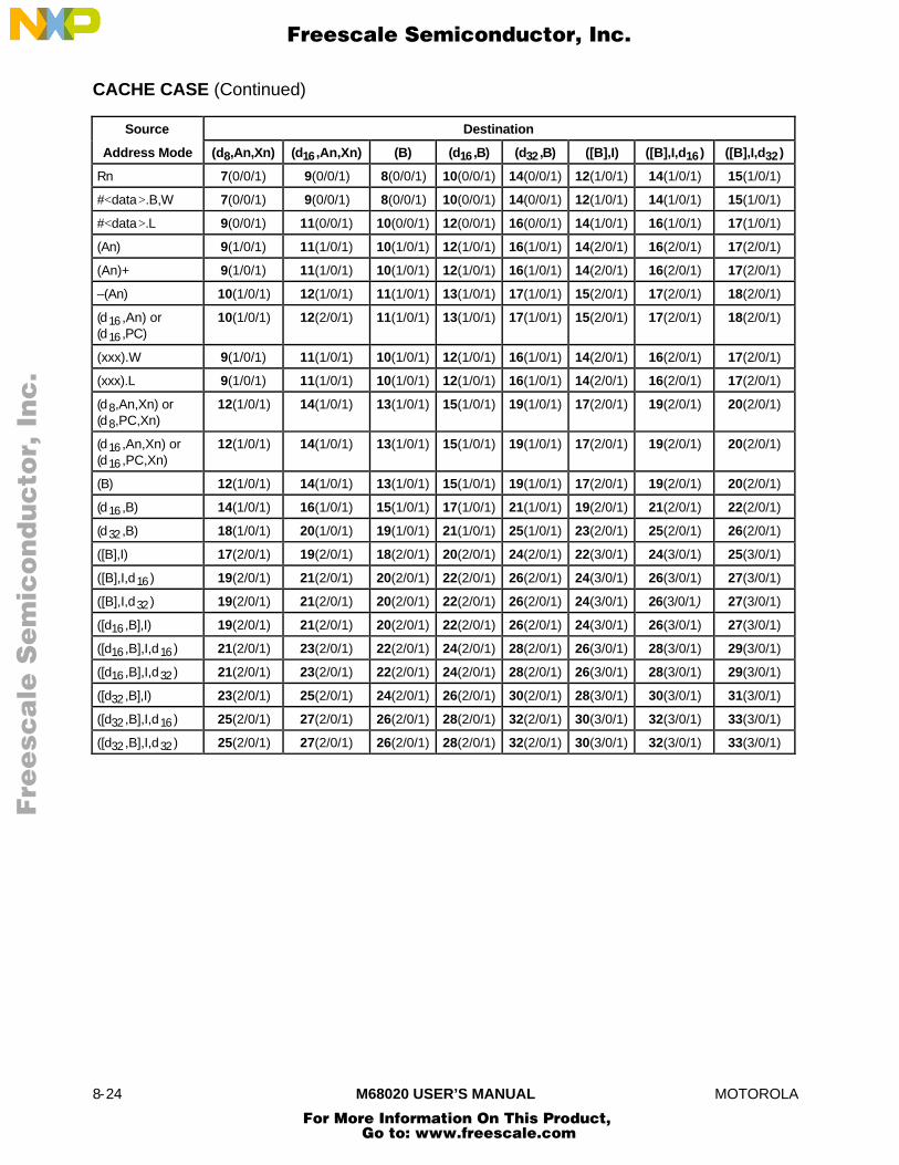
8-24 M68020 USER’S MANUAL MOTOROLA
CACHE CASE (Continued)
Source Destination
Address Mode (d8,An,Xn) (d16,An,Xn) (B) (d16,B) (d32,B) ([B],I) ([B],I,d16) ([B],I,d32)
Rn 7(0/0/1) 9(0/0/1) 8(0/0/1) 10(0/0/1) 14(0/0/1) 12(1/0/1) 14(1/0/1) 15(1/0/1)
#<data>.B,W 7(0/0/1) 9(0/0/1) 8(0/0/1) 10(0/0/1) 14(0/0/1) 12(1/0/1) 14(1/0/1) 15(1/0/1)
#<data>.L 9(0/0/1) 11(0/0/1) 10(0/0/1) 12(0/0/1) 16(0/0/1) 14(1/0/1) 16(1/0/1) 17(1/0/1)
(An) 9(1/0/1) 11(1/0/1) 10(1/0/1) 12(1/0/1) 16(1/0/1) 14(2/0/1) 16(2/0/1) 17(2/0/1)
(An)+ 9(1/0/1) 11(1/0/1) 10(1/0/1) 12(1/0/1) 16(1/0/1) 14(2/0/1) 16(2/0/1) 17(2/0/1)
–(An) 10(1/0/1) 12(1/0/1) 11(1/0/1) 13(1/0/1) 17(1/0/1) 15(2/0/1) 17(2/0/1) 18(2/0/1)
(d16,An) or(d16,PC)
10(1/0/1) 12(2/0/1) 11(1/0/1) 13(1/0/1) 17(1/0/1) 15(2/0/1) 17(2/0/1) 18(2/0/1)
(xxx).W 9(1/0/1) 11(1/0/1) 10(1/0/1) 12(1/0/1) 16(1/0/1) 14(2/0/1) 16(2/0/1) 17(2/0/1)
(xxx).L 9(1/0/1) 11(1/0/1) 10(1/0/1) 12(1/0/1) 16(1/0/1) 14(2/0/1) 16(2/0/1) 17(2/0/1)
(d8,An,Xn) or(d8,PC,Xn)
12(1/0/1) 14(1/0/1) 13(1/0/1) 15(1/0/1) 19(1/0/1) 17(2/0/1) 19(2/0/1) 20(2/0/1)
(d16,An,Xn) or(d16,PC,Xn)
12(1/0/1) 14(1/0/1) 13(1/0/1) 15(1/0/1) 19(1/0/1) 17(2/0/1) 19(2/0/1) 20(2/0/1)
(B) 12(1/0/1) 14(1/0/1) 13(1/0/1) 15(1/0/1) 19(1/0/1) 17(2/0/1) 19(2/0/1) 20(2/0/1)
(d16,B) 14(1/0/1) 16(1/0/1) 15(1/0/1) 17(1/0/1) 21(1/0/1) 19(2/0/1) 21(2/0/1) 22(2/0/1)
(d32,B) 18(1/0/1) 20(1/0/1) 19(1/0/1) 21(1/0/1) 25(1/0/1) 23(2/0/1) 25(2/0/1) 26(2/0/1)
([B],I) 17(2/0/1) 19(2/0/1) 18(2/0/1) 20(2/0/1) 24(2/0/1) 22(3/0/1) 24(3/0/1) 25(3/0/1)
([B],I,d16) 19(2/0/1) 21(2/0/1) 20(2/0/1) 22(2/0/1) 26(2/0/1) 24(3/0/1) 26(3/0/1) 27(3/0/1)
([B],I,d32) 19(2/0/1) 21(2/0/1) 20(2/0/1) 22(2/0/1) 26(2/0/1) 24(3/0/1) 26(3/0/1) 27(3/0/1)
([d16,B],I) 19(2/0/1) 21(2/0/1) 20(2/0/1) 22(2/0/1) 26(2/0/1) 24(3/0/1) 26(3/0/1) 27(3/0/1)
([d16,B],I,d16) 21(2/0/1) 23(2/0/1) 22(2/0/1) 24(2/0/1) 28(2/0/1) 26(3/0/1) 28(3/0/1) 29(3/0/1)
([d16,B],I,d32) 21(2/0/1) 23(2/0/1) 22(2/0/1) 24(2/0/1) 28(2/0/1) 26(3/0/1) 28(3/0/1) 29(3/0/1)
([d32,B],I) 23(2/0/1) 25(2/0/1) 24(2/0/1) 26(2/0/1) 30(2/0/1) 28(3/0/1) 30(3/0/1) 31(3/0/1)
([d32,B],I,d16) 25(2/0/1) 27(2/0/1) 26(2/0/1) 28(2/0/1) 32(2/0/1) 30(3/0/1) 32(3/0/1) 33(3/0/1)
([d32,B],I,d32) 25(2/0/1) 27(2/0/1) 26(2/0/1) 28(2/0/1) 32(2/0/1) 30(3/0/1) 32(3/0/1) 33(3/0/1)
Fre
esc
ale
Se
mic
on
du
cto
r, I
Freescale Semiconductor, Inc.
For More Information On This Product, Go to: www.freescale.com
nc
...

MOTOROLA M68020 USER’S MANUAL 8-25
CACHE CASE (Concluded)
Source Destination
Address Mode ([d16,B],I) ([d16,B],I,d16) ([d16,B],I,d32) ([d32,B],I) ([d32,B],I,d16) ([d32,B],I,d32)
Rn 14(1/0/1) 16(1/0/1) 17(1/0/1) 18(1/0/1) 20(1/0/1) 21(1/0/1)
#<data>.B,W 14(1/0/1) 16(1/0/1) 17(1/0/1) 18(1/0/1) 20(1/0/1) 21(1/0/1)
#<data>.L 16(1/0/1) 18(1/0/1) 19(1/0/1) 20(1/0/1) 22(1/0/1) 23(1/0/1)
(An) 16(2/0/1) 18(2/0/1) 19(2/0/1) 20(2/0/1) 22(2/0/1) 23(2/0/1)
(An)+ 16(2/0/1) 18(2/0/1) 19(2/0/1) 20(2/0/1) 22(2/0/1) 23(2/0/1)
–(An) 17(2/0/1) 19(2/0/1) 20(2/0/1) 21(2/0/1) 23(2/0/1) 24(2/0/1)
(d16,An) or (d16,PC) 17(2/0/1) 19(2/0/1) 20(2/0/1) 21(2/0/1) 23(2/0/1) 24(2/0/1)
(xxx).W 16(2/0/1) 18(2/0/1) 19(2/0/1) 20(2/0/1) 22(2/0/1) 23(2/0/1)
(xxx).L 16(2/0/1) 18(2/0/1) 19(2/0/1) 20(2/0/1) 22(2/0/1) 23(2/0/1)
(d8,An,Xn) or(d8,PC,Xn)
19(2/0/1) 21(2/0/1) 22(2/0/1) 23(2/0/1) 25(2/0/1) 26(2/0/1)
(d16,An,Xn) or(d16,PC,Xn)
19(2/0/1) 21(2/0/1) 22(2/0/1) 23(2/0/1) 25(2/0/1) 26(2/0/1)
(B) 19(2/0/1) 21(2/0/1) 22(2/0/1) 23(2/0/1) 25(2/0/1) 26(2/0/1)
(d16,B) 21(2/0/1) 23(2/0/1) 24(2/0/1) 25(2/0/1) 27(2/0/1) 28(2/0/1)
(d32,B) 25(2/0/1) 27(2/0/1) 28(2/0/1) 29(2/0/1) 31(2/0/1) 32(2/0/1)
([B],I) 24(3/0/1) 26(3/0/1) 27(3/0/1) 28(3/0/1) 30(3/0/1) 31(3/0/1)
([B],I,d16) 26(3/0/1) 28(3/0/1) 29(3/0/1) 30(3/0/1) 32(3/0/1) 33(3/0/1)
([B],I,d32) 26(3/0/1) 28(3/0/1) 29(3/0/1) 30(3/0/1) 32(3/0/1) 33(3/0/1)
([d16,B],I) 26(3/0/1) 28(3/0/1) 29(3/0/1) 30(3/0/1) 32(3/0/1) 33(3/0/1)
([d16,B],I,d16) 28(3/0/1) 30(3/0/1) 31(3/0/1) 32(3/0/1) 34(3/0/1) 35(3/0/1)
([d16,B],I,d32) 28(3/0/1) 30(3/0/1) 31(3/0/1) 32(3/0/1) 34(3/0/1) 35(3/0/1)
([d32,B],I) 30(3/0/1) 32(3/0/1) 33(3/0/1) 34(3/0/1) 36(3/0/1) 37(3/0/1)
([d32,B],I,d16) 32(3/0/1) 34(3/0/1) 35(3/0/1) 36(3/0/1) 38(3/0/1) 39(3/0/1)
([d32,B],I,d32) 32(3/0/1) 34(3/0/1) 35(3/0/1) 36(3/0/1) 38(3/0/1) 39(3/0/1)
Fre
esc
ale
Se
mic
on
du
cto
r, I
Freescale Semiconductor, Inc.
For More Information On This Product, Go to: www.freescale.com
nc
...
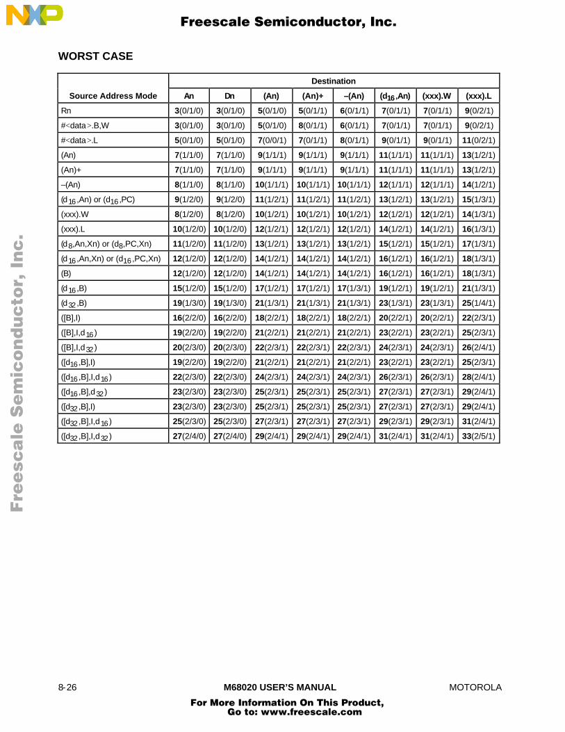
8-26 M68020 USER’S MANUAL MOTOROLA
WORST CASE
Destination
Source Address Mode An Dn (An) (An)+ –(An) (d16,An) (xxx).W (xxx).L
Rn 3(0/1/0) 3(0/1/0) 5(0/1/0) 5(0/1/1) 6(0/1/1) 7(0/1/1) 7(0/1/1) 9(0/2/1)
#<data>.B,W 3(0/1/0) 3(0/1/0) 5(0/1/0) 8(0/1/1) 6(0/1/1) 7(0/1/1) 7(0/1/1) 9(0/2/1)
#<data>.L 5(0/1/0) 5(0/1/0) 7(0/0/1) 7(0/1/1) 8(0/1/1) 9(0/1/1) 9(0/1/1) 11(0/2/1)
(An) 7(1/1/0) 7(1/1/0) 9(1/1/1) 9(1/1/1) 9(1/1/1) 11(1/1/1) 11(1/1/1) 13(1/2/1)
(An)+ 7(1/1/0) 7(1/1/0) 9(1/1/1) 9(1/1/1) 9(1/1/1) 11(1/1/1) 11(1/1/1) 13(1/2/1)
–(An) 8(1/1/0) 8(1/1/0) 10(1/1/1) 10(1/1/1) 10(1/1/1) 12(1/1/1) 12(1/1/1) 14(1/2/1)
(d16,An) or (d16,PC) 9(1/2/0) 9(1/2/0) 11(1/2/1) 11(1/2/1) 11(1/2/1) 13(1/2/1) 13(1/2/1) 15(1/3/1)
(xxx).W 8(1/2/0) 8(1/2/0) 10(1/2/1) 10(1/2/1) 10(1/2/1) 12(1/2/1) 12(1/2/1) 14(1/3/1)
(xxx).L 10(1/2/0) 10(1/2/0) 12(1/2/1) 12(1/2/1) 12(1/2/1) 14(1/2/1) 14(1/2/1) 16(1/3/1)
(d8,An,Xn) or (d8,PC,Xn) 11(1/2/0) 11(1/2/0) 13(1/2/1) 13(1/2/1) 13(1/2/1) 15(1/2/1) 15(1/2/1) 17(1/3/1)
(d16,An,Xn) or (d16,PC,Xn) 12(1/2/0) 12(1/2/0) 14(1/2/1) 14(1/2/1) 14(1/2/1) 16(1/2/1) 16(1/2/1) 18(1/3/1)
(B) 12(1/2/0) 12(1/2/0) 14(1/2/1) 14(1/2/1) 14(1/2/1) 16(1/2/1) 16(1/2/1) 18(1/3/1)
(d16,B) 15(1/2/0) 15(1/2/0) 17(1/2/1) 17(1/2/1) 17(1/3/1) 19(1/2/1) 19(1/2/1) 21(1/3/1)
(d32,B) 19(1/3/0) 19(1/3/0) 21(1/3/1) 21(1/3/1) 21(1/3/1) 23(1/3/1) 23(1/3/1) 25(1/4/1)
([B],I) 16(2/2/0) 16(2/2/0) 18(2/2/1) 18(2/2/1) 18(2/2/1) 20(2/2/1) 20(2/2/1) 22(2/3/1)
([B],I,d16) 19(2/2/0) 19(2/2/0) 21(2/2/1) 21(2/2/1) 21(2/2/1) 23(2/2/1) 23(2/2/1) 25(2/3/1)
([B],I,d32) 20(2/3/0) 20(2/3/0) 22(2/3/1) 22(2/3/1) 22(2/3/1) 24(2/3/1) 24(2/3/1) 26(2/4/1)
([d16,B],I) 19(2/2/0) 19(2/2/0) 21(2/2/1) 21(2/2/1) 21(2/2/1) 23(2/2/1) 23(2/2/1) 25(2/3/1)
([d16,B],I,d16) 22(2/3/0) 22(2/3/0) 24(2/3/1) 24(2/3/1) 24(2/3/1) 26(2/3/1) 26(2/3/1) 28(2/4/1)
([d16,B],d32) 23(2/3/0) 23(2/3/0) 25(2/3/1) 25(2/3/1) 25(2/3/1) 27(2/3/1) 27(2/3/1) 29(2/4/1)
([d32,B],I) 23(2/3/0) 23(2/3/0) 25(2/3/1) 25(2/3/1) 25(2/3/1) 27(2/3/1) 27(2/3/1) 29(2/4/1)
([d32,B],I,d16) 25(2/3/0) 25(2/3/0) 27(2/3/1) 27(2/3/1) 27(2/3/1) 29(2/3/1) 29(2/3/1) 31(2/4/1)
([d32,B],I,d32) 27(2/4/0) 27(2/4/0) 29(2/4/1) 29(2/4/1) 29(2/4/1) 31(2/4/1) 31(2/4/1) 33(2/5/1)
Fre
esc
ale
Se
mic
on
du
cto
r, I
Freescale Semiconductor, Inc.
For More Information On This Product, Go to: www.freescale.com
nc
...
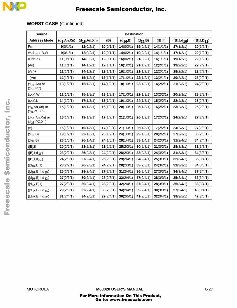
MOTOROLA M68020 USER’S MANUAL 8-27
WORST CASE (Continued)
Source Destination
Address Mode (d8,An,Xn) (d16,An,Xn) (B) (d16,B) (d32,B) ([B],I) ([B],I,d16) ([B],I,D32)
Rn 9(0/1/1) 12(0/2/1) 10(0/1/1) 14(0/2/1) 19(0/2/1) 14(1/1/1) 17(1/2/1) 20(1/2/1)
#<data>.B,W 9(0/1/1) 12(0/2/1) 10(0/1/1) 14(0/2/1) 19(0/2/1) 14(1/1/1) 17(1/2/1) 20(1/2/1)
#<data>.L 11(0/1/1) 14(0/2/1) 12(0/1/1) 16(0/2/1) 21(0/2/1) 16(1/1/1) 19(1/2/1) 22(1/2/1)
(An) 11(1/1/1) 14(1/2/1) 12(1/1/1) 16(1/2/1) 21(1/2/1) 12(2/1/1) 19(2/2/1) 22(2/2/1)
(An)+ 11(1/1/1) 14(1/2/1) 12(1/1/1) 16(1/2/1) 21(1/2/1) 12(2/1/1) 19(2/2/1) 22(2/2/1)
–(An) 12(1/1/1) 15(1/2/1) 13(1/1/1) 17(1/2/1) 22(1/2/1) 13(2/1/1) 20(2/2/1) 23(2/2/1)
(d16,An) or(d16,PC)
13(1/2/1) 16(1/3/1) 14(1/2/1) 18(1/3/1) 23(1/3/1) 14(2/2/1) 21(2/3/1) 24(2/3/1)
(xxx).W 12(1/2/1) 15(1/3/1) 13(1/2/1) 17(1/3/1) 22(1/3/1) 13(2/2/1) 20(2/3/1) 23(2/3/1)
(xxx).L 14(1/2/1) 17(1/3/1) 15(1/2/1) 19(1/3/1) 24(1/3/1) 15(2/2/1) 22(2/3/1) 25(2/3/1)
(d8,An,Xn) or(d8,PC,Xn)
15(1/2/1) 18(1/3/1) 16(1/2/1) 20(1/3/1) 25(1/3/1) 16(2/2/1) 23(2/3/1) 26(2/3/1)
(d16,An,Xn) or(d16,PC,Xn)
16(1/2/1) 19(1/3/1) 17(1/2/1) 21(1/3/1) 26(1/3/1) 17(2/2/1) 24(2/3/1) 27(2/3/1)
(B) 16(1/2/1) 19(1/3/1) 17(1/2/1) 21(1/3/1) 26(1/3/1) 17(2/2/1) 24(2/3/1) 27(2/3/1)
(d16,B) 19(1/2/1) 22(1/3/1) 20(1/2/1) 24(1/3/1) 29(1/3/1) 20(2/2/1) 27(2/3/1) 30(2/3/1)
(d32,B) 23(1/3/1) 26(1/4/1) 24(1/3/1) 28(1/4/1) 33(1/4/1) 24(2/3/1) 31(2/4/1) 34(2/4/1)
([B],I) 20(2/2/1) 23(2/3/1) 21(2/2/1) 25(2/3/1) 30(2/3/1) 21(3/2/1) 28(3/3/1) 31(3/3/1)
([B],I,d16) 23(2/2/1) 26(2/3/1) 24(2/2/1) 28(2/3/1) 33(2/3/1) 24(3/2/1) 31(3/3/1) 34(3/3/1)
([B],I,d32) 24(2/3/1) 27(2/4/1) 25(2/3/1) 29(2/4/1) 34(2/4/1) 25(3/3/1) 32(3/4/1) 35(3/4/1)
([d16,B],I) 23(2/2/1) 26(2/3/1) 24(2/2/1) 28(2/3/1) 33(2/3/1) 24(3/2/1) 31(3/3/1) 34(3/3/1)
([d16,B],I,d16) 26(2/3/1) 29(2/4/1) 27(2/3/1) 31(2/4/1) 36(2/4/1) 27(3/3/1) 34(3/4/1) 37(3/4/1)
([d16,B],I,d32) 27(2/3/1) 30(2/4/1) 28(2/3/1) 32(2/4/1) 37(2/4/1) 28(3/3/1) 35(3/4/1) 38(3/4/1)
([d32,B],I) 27(2/3/1) 30(2/4/1) 28(2/3/1) 32(2/4/1) 37(2/4/1) 28(3/3/1) 35(3/4/1) 38(3/4/1)
([d32,B],I,d16) 29(2/3/1) 32(2/4/1) 30(2/3/1) 34(2/4/1) 39(2/4/1) 30(3/3/1) 37(3/4/1) 40(3/4/1)
([d32,B],I,d32) 31(2/4/1) 34(2/5/1) 32(2/4/1) 36(2/5/1) 41(2/5/1) 32(3/4/1) 39(3/5/1) 42(3/5/1)
Fre
esc
ale
Se
mic
on
du
cto
r, I
Freescale Semiconductor, Inc.
For More Information On This Product, Go to: www.freescale.com
nc
...

8-28 M68020 USER’S MANUAL MOTOROLA
WORST CASE (Concluded)
Source Destination
Address Mode ([d16,B],I) ([d16,B],I,d16) ([d16,B],I,d32) ([d32,B],I) ([d32,B],I,d16) ([d32,B],I,d32)
Rn 17(1/2/1) 20(1/2/1) 23(1/3/1) 22(1/2/1) 25(1/3/1) 27(1/3/1)
#<data>.B,W 17(1/2/1) 20(1/2/1) 23(1/3/1) 22(1/2/1) 25(1/3/1) 27(1/3/1)
#<data>.L 19(1/2/1) 22(1/2/1) 25(1/3/1) 24(1/2/1) 27(1/3/1) 29(1/3/1)
(An) 19(2/2/1) 22(2/2/1) 25(2/3/1) 24(2/2/1) 27(2/3/1) 29(2/3/1)
(An)+ 19(2/2/1) 22(2/2/1) 25(2/3/1) 24(2/2/1) 27(2/3/1) 29(2/3/1)
–(An) 20(2/2/1) 23(2/2/1) 26(2/3/1) 25(2/2/1) 28(2/3/1) 30(2/3/1)
(d16,An) or (d16,PC) 21(2/3/1) 24(2/3/1) 27(2/4/1) 26(2/3/1) 29(2/4/1) 31(2/4/1)
(xxx).W 20(2/3/1) 23(2/3/1) 26(2/4/1) 27(2/3/1) 28(2/4/1) 30(2/4/1)
(xxx).L 22(2/3/1) 25(2/3/1) 28(2/4/1) 29(2/3/1) 30(2/4/1) 32(2/4/1)
(d8,An,Xn) or(d8,PC,Xn)
23(2/3/1) 26(2/3/1) 29(2/4/1) 30(2/3/1) 31(2/4/1) 33(2/4/1)
(d16,An,Xn) or(d16,PC,Xn)
24(2/3/1) 27(2/3/1) 30(2/4/1) 31(2/3/1) 32(2/4/1) 34(2/4/1)
(B) 24(2/3/1) 27(2/3/1) 30(2/4/1) 31(2/3/1) 32(2/4/1) 34(2/4/1)
(d16,B) 27(2/3/1) 30(2/3/1) 33(2/4/1) 34(2/3/1) 35(2/4/1) 37(2/4/1)
(d32,B) 31(2/4/1) 34(2/4/1) 37(2/5/1) 38(2/4/1) 39(2/5/1) 41(2/5/1)
([B],I) 28(3/3/1) 31(3/3/1) 34(3/4/1) 35(3/3/1) 36(3/4/1) 38(3/4/1)
([B],I,d16) 31(3/3/1) 34(3/3/1) 37(3/4/1) 38(3/3/1) 39(3/4/1) 41(3/4/1)
([B],I,d32) 32(3/4/1) 35(3/4/1) 38(3/5/1) 39(3/4/1) 40(3/5/1) 42(3/5/1)
([d16,B],I) 31(3/3/1) 34(3/3/1) 37(3/4/1) 38(3/3/1) 39(3/4/1) 41(3/4/1)
([d16,B],I,d16) 34(3/4/1) 37(3/4/1) 40(3/5/1) 41(3/4/1) 42(3/5/1) 44(3/5/1)
([d16,B],I,d32) 35(3/4/1) 38(3/4/1) 41(3/5/1) 42(3/4/1) 43(3/5/1) 45(3/5/1)
([d32,B],I) 35(3/4/1) 38(3/4/1) 41(3/5/1) 42(3/4/1) 43(3/5/1) 45(3/5/1)
([d32,B],I,d16) 37(3/4/1) 40(3/4/1) 43(3/5/1) 44(3/4/1) 45(3/5/1) 47(3/5/1)
([d32,B],I,d32) 39(3/5/1) 42(3/5/1) 45(3/6/1) 46(3/5/1) 47(3/6/1) 49(3/6/1)
Fre
esc
ale
Se
mic
on
du
cto
r, I
Freescale Semiconductor, Inc.
For More Information On This Product, Go to: www.freescale.com
nc
...
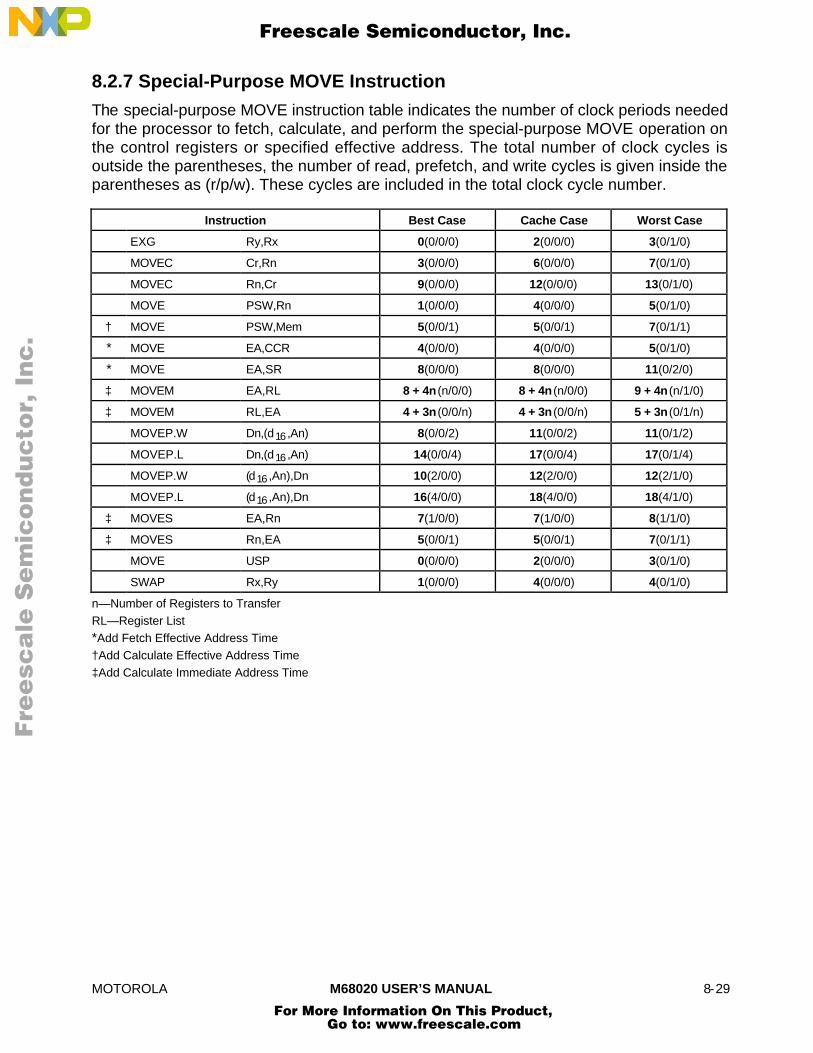
MOTOROLA M68020 USER’S MANUAL 8-29
8.2.7 Special-Purpose MOVE Instruction
The special-purpose MOVE instruction table indicates the number of clock periods neededfor the processor to fetch, calculate, and perform the special-purpose MOVE operation onthe control registers or specified effective address. The total number of clock cycles isoutside the parentheses, the number of read, prefetch, and write cycles is given inside theparentheses as (r/p/w). These cycles are included in the total clock cycle number.
Instruction Best Case Cache Case Worst Case
EXG Ry,Rx 0(0/0/0) 2(0/0/0) 3(0/1/0)
MOVEC Cr,Rn 3(0/0/0) 6(0/0/0) 7(0/1/0)
MOVEC Rn,Cr 9(0/0/0) 12(0/0/0) 13(0/1/0)
MOVE PSW,Rn 1(0/0/0) 4(0/0/0) 5(0/1/0)
† MOVE PSW,Mem 5(0/0/1) 5(0/0/1) 7(0/1/1)
* MOVE EA,CCR 4(0/0/0) 4(0/0/0) 5(0/1/0)
* MOVE EA,SR 8(0/0/0) 8(0/0/0) 11(0/2/0)
‡ MOVEM EA,RL 8 + 4n (n/0/0) 8 + 4n (n/0/0) 9 + 4n (n/1/0)
‡ MOVEM RL,EA 4 + 3n (0/0/n) 4 + 3n (0/0/n) 5 + 3n (0/1/n)
MOVEP.W Dn,(d16,An) 8(0/0/2) 11(0/0/2) 11(0/1/2)
MOVEP.L Dn,(d16,An) 14(0/0/4) 17(0/0/4) 17(0/1/4)
MOVEP.W (d16,An),Dn 10(2/0/0) 12(2/0/0) 12(2/1/0)
MOVEP.L (d16,An),Dn 16(4/0/0) 18(4/0/0) 18(4/1/0)
‡ MOVES EA,Rn 7(1/0/0) 7(1/0/0) 8(1/1/0)
‡ MOVES Rn,EA 5(0/0/1) 5(0/0/1) 7(0/1/1)
MOVE USP 0(0/0/0) 2(0/0/0) 3(0/1/0)
SWAP Rx,Ry 1(0/0/0) 4(0/0/0) 4(0/1/0)
n—Number of Registers to TransferRL—Register List*Add Fetch Effective Address Time†Add Calculate Effective Address Time‡Add Calculate Immediate Address Time
Fre
esc
ale
Se
mic
on
du
cto
r, I
Freescale Semiconductor, Inc.
For More Information On This Product, Go to: www.freescale.com
nc
...
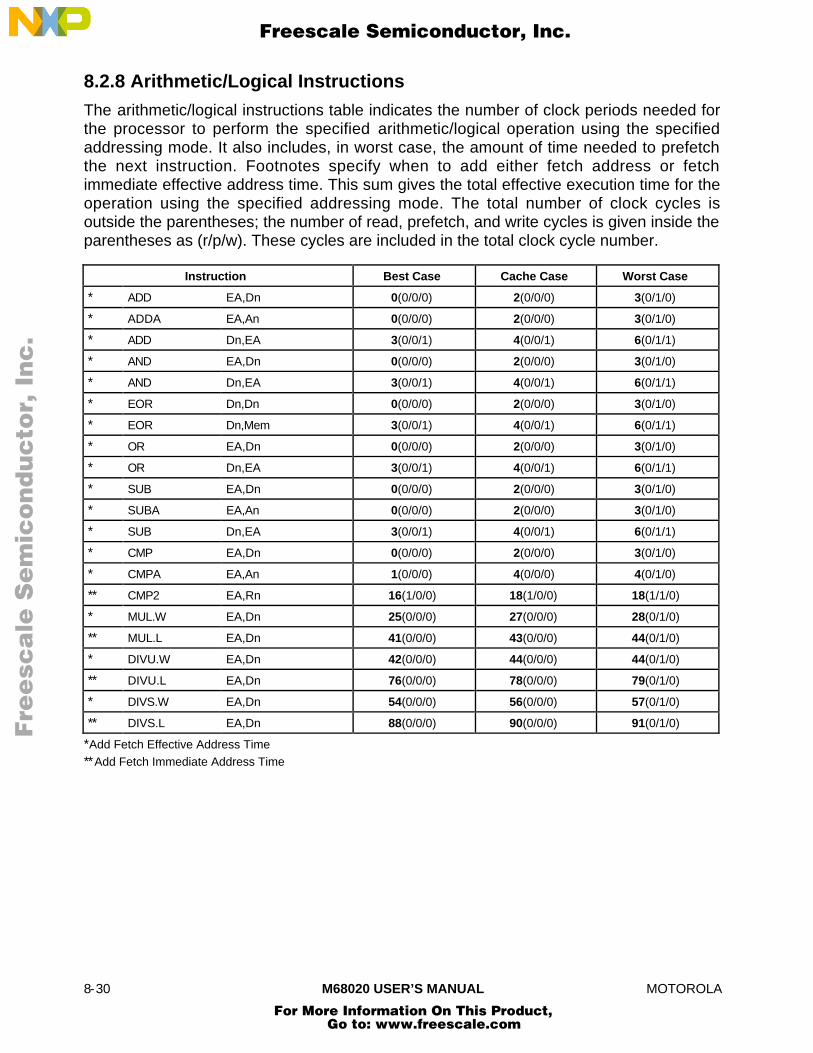
8-30 M68020 USER’S MANUAL MOTOROLA
8.2.8 Arithmetic/Logical Instructions
The arithmetic/logical instructions table indicates the number of clock periods needed forthe processor to perform the specified arithmetic/logical operation using the specifiedaddressing mode. It also includes, in worst case, the amount of time needed to prefetchthe next instruction. Footnotes specify when to add either fetch address or fetchimmediate effective address time. This sum gives the total effective execution time for theoperation using the specified addressing mode. The total number of clock cycles isoutside the parentheses; the number of read, prefetch, and write cycles is given inside theparentheses as (r/p/w). These cycles are included in the total clock cycle number.
Instruction Best Case Cache Case Worst Case
* ADD EA,Dn 0(0/0/0) 2(0/0/0) 3(0/1/0)
* ADDA EA,An 0(0/0/0) 2(0/0/0) 3(0/1/0)
* ADD Dn,EA 3(0/0/1) 4(0/0/1) 6(0/1/1)
* AND EA,Dn 0(0/0/0) 2(0/0/0) 3(0/1/0)
* AND Dn,EA 3(0/0/1) 4(0/0/1) 6(0/1/1)
* EOR Dn,Dn 0(0/0/0) 2(0/0/0) 3(0/1/0)
* EOR Dn,Mem 3(0/0/1) 4(0/0/1) 6(0/1/1)
* OR EA,Dn 0(0/0/0) 2(0/0/0) 3(0/1/0)
* OR Dn,EA 3(0/0/1) 4(0/0/1) 6(0/1/1)
* SUB EA,Dn 0(0/0/0) 2(0/0/0) 3(0/1/0)
* SUBA EA,An 0(0/0/0) 2(0/0/0) 3(0/1/0)
* SUB Dn,EA 3(0/0/1) 4(0/0/1) 6(0/1/1)
* CMP EA,Dn 0(0/0/0) 2(0/0/0) 3(0/1/0)
* CMPA EA,An 1(0/0/0) 4(0/0/0) 4(0/1/0)
** CMP2 EA,Rn 16(1/0/0) 18(1/0/0) 18(1/1/0)
* MUL.W EA,Dn 25(0/0/0) 27(0/0/0) 28(0/1/0)
** MUL.L EA,Dn 41(0/0/0) 43(0/0/0) 44(0/1/0)
* DIVU.W EA,Dn 42(0/0/0) 44(0/0/0) 44(0/1/0)
** DIVU.L EA,Dn 76(0/0/0) 78(0/0/0) 79(0/1/0)
* DIVS.W EA,Dn 54(0/0/0) 56(0/0/0) 57(0/1/0)
** DIVS.L EA,Dn 88(0/0/0) 90(0/0/0) 91(0/1/0)
*Add Fetch Effective Address Time**Add Fetch Immediate Address Time
Fre
esc
ale
Se
mic
on
du
cto
r, I
Freescale Semiconductor, Inc.
For More Information On This Product, Go to: www.freescale.com
nc
...

MOTOROLA M68020 USER’S MANUAL 8-31
8.2.9 Immediate Arithmetic/Logical Instructions
The immediate arithmetic/logical instructions table indicates the number of clock periodsneeded for the processor to fetch the source immediate data value and perform thespecified arithmetic/logical operation using the specified destination addressing mode.Footnotes indicate when to add appropriate fetch effective or fetch immediate effectiveaddress time. This computation will give the total execution time needed to perform theappropriate immediate arithmetic/logical operation. The total number of clock cycles isoutside the parentheses; the number of read, prefetch, and write cycles is given inside theparentheses as (r/p/w). These cycles are included in the total clock cycle number.
Instruction Best Case Cache Case Worst Case
MOVEQ #<data>,Dn 0(0/0/0) 2(0/0/0) 3(0/1/0)
ADDQ #<data>,Rn 0(0/0/0) 2(0/0/0) 3(0/1/0)
* ADDQ #<data>,Mem 3(0/0/1) 4(0/0/1) 6(0/1/1)
SUBQ #<data>,Rn 0(0/0/0) 2(0/0/0) 3(0/1/0)
* SUBQ #<data>,Mem 3(0/0/1) 4(0/0/1) 6(0/1/1)
** ADDI #<data>,Dn 0(0/0/0) 2(0/0/0) 3(0/1/0)
** ADDI #<data>,Mem 3(0/0/1) 4(0/0/1) 6(0/1/1)
** ANDI #<data>,Dn 0(0/0/0) 2(0/0/0) 3(0/1/0)
** ANDI #<data>,Mem 3(0/0/1) 4(0/0/1) 6(0/1/1)
** EORI #<data>,Dn 0(0/0/0) 2(0/0/0) 3(0/1/0)
** EORI #<data>,Mem 3(0/0/1) 4(0/0/1) 6(0/1/1)
** ORI #<data>,Dn 0(0/0/0) 2(0/0/0) 3(0/1/0)
** ORI #<data>,Mem 3(0/0/1) 4(0/0/1) 6(0/1/1)
** SUBI #<data>,Dn 0(0/0/0) 2(0/0/0) 3(0/1/0)
** SUBI #<data>,Mem 3(0/0/1) 4(0/0/1) 6(0/1/1)
** CMPI #<data>,EA 0(0/0/0) 2(0/0/0) 3(0/1/0)
*Add Fetch Effective Address Time**Add Fetch Immediate Address Time
Fre
esc
ale
Se
mic
on
du
cto
r, I
Freescale Semiconductor, Inc.
For More Information On This Product, Go to: www.freescale.com
nc
...

8-32 M68020 USER’S MANUAL MOTOROLA
8.2.10 Binary-Coded Decimal Operations
The binary-coded decimal operations table indicates the number of clock periods neededfor the processor to perform the specified operation using the given addressing modes,with complete execution times given. No additional tables are needed to calculate totaleffective execution time for these instructions. The total number of clock cycles is outsidethe parentheses; the number of read, prefetch, and write cycles is given inside theparentheses as (r/p/w). These cycles are included in the total clock cycle number.
Instruction Best Case Cache Case Worst Case
ABCD Dn,Dn 4(0/0/0) 4(0/0/0) 5(0/1/0)
ABCD –(An),–(An) 14(2/0/1) 16(2/0/1) 17(2/1/1)
SBCD Dn,Dn 4(0/0/0) 4(0/0/0) 5(0/1/0)
SBCD –(An),–(An) 14(2/0/1) 16(2/0/1) 17(2/1/1)
ADDX Dn,Dn 2(0/0/0) 2(0/0/0) 3(0/1/0)
ADDX –(An),–(An) 10(2/0/1) 12(2/0/1) 13(2/1/1)
SUBX Dn,Dn 2(0/0/0) 2(0/0/0) 3(0/1/0)
SUBX –(An),–(An) 10(2/0/1) 12(2/0/1) 13(2/1/1)
CMPM (An)+,(An)+ 8(2/0/0) 9(2/0/0) 10(2/1/0)
PACK Dn,Dn,#<data> 3(0/0/0) 6(0/0/0) 7(0/1/0)
PACK –(An),–(An),#<data> 11(1/0/1) 13(1/0/1) 13(1/1/1)
UNPK Dn,Dn,#<data> 5(0/0/0) 8(0/0/0) 9(0/1/0)
UNPK –(An),–(An),#<data> 11(1/0/1) 13(1/0/1) 13(1/1/1)
Fre
esc
ale
Se
mic
on
du
cto
r, I
Freescale Semiconductor, Inc.
For More Information On This Product, Go to: www.freescale.com
nc
...

MOTOROLA M68020 USER’S MANUAL 8-33
8.2.11 Single-Operand Instructions
The single-operand instructions table indicates the number of clock periods needed for theprocessor to perform the specified operation on the given addressing mode. Footnotesindicate when it is necessary to add another table entry to calculate the total effectiveexecution time for the instruction. The total number of clock cycles is outside theparentheses; the number of read, prefetch, and write cycles is given inside theparentheses as (r/p/w). These cycles are included in the total clock cycle number.
Instruction Best Case Cache Case Worst Case
CLR Dn 0(0/0/0) 2(0/0/0) 3(0/1/0)
† CLR Mem 3(0/0/1) 4(0/0/1) 6(0/1/1)
NEG Dn 0(0/0/0) 2(0/0/0) 3(0/1/0)
* NEG Mem 3(0/0/1) 4(0/0/1) 6(0/1/1)
NEGX Dn 0(0/0/0) 2(0/0/0) 3(0/1/0)
* NEGX Mem 3(0/0/1) 4(0/0/1) 6(0/1/1)
NOT Dn 0(0/0/0) 2(0/0/0) 3(0/1/0)
* NOT Mem 3(0/0/1) 4(0/0/1) 6(0/1/1)
EXT Dn 1(0/0/0) 4(0/0/0) 4(0/1/0)
NBCD Dn 6(0/0/0) 6(0/0/0) 6(0/1/0)
Scc Dn 1(0/0/0) 4(0/0/0) 4(0/1/0)
† Scc Mem 6(0/0/1) 6(0/0/1) 6(0/1/1)
TAS Dn 1(0/0/0) 4(0/0/0) 4(0/1/0)
† TAS Mem 12(1/0/1) 12(1/0/1) 13(1/1/1)
* TST EA 0(0/0/0) 2(0/0/0) 3(0/1/0)
*Add Fetch Effective Address Time†Add Calculate Effective Address Time
Fre
esc
ale
Se
mic
on
du
cto
r, I
Freescale Semiconductor, Inc.
For More Information On This Product, Go to: www.freescale.com
nc
...

8-34 M68020 USER’S MANUAL MOTOROLA
8.2.12 Shift/Rotate Instructions
The shift/rotate instructions table indicates the number of clock periods needed for theprocessor to perform the specified operation on the given addressing mode. Footnotesindicate when it is necessary to add another table entry to calculate the total effectiveexecution time for the instruction. The number of bits shifted does not affect executiontime. The total number of clock cycles is outside the parentheses, the number of read,prefetch, and write cycles is given inside the parentheses as (r/p/w). These cycles areincluded in the total clock cycle number.
Instruction Best Case Cache Case Worst Case
LSL Dn (Static) 1(0/0/0) 4(0/0/0) 4(0/1/0)
LSR Dn (Static) 1(0/0/0) 4(0/0/0) 4(0/1/0)
LSL Dn (Dynamic) 3(0/0/0) 6(0/0/0) 6(0/1/0)
LSR Dn (Dynamic) 3(0/0/0) 6(0/0/0) 6(0/1/0)
* LSL Mem by 1 5(0/0/1) 5(0/0/1) 6(0/1/1)
* LSR Mem by 1 5(0/0/1) 5(0/0/1) 6(0/1/1)
ASL Dn 5(0/0/0) 8(0/0/0) 8(0/1/0)
ASR Dn 3(0/0/0) 6(0/0/0) 6(0/1/0)
* ASL Mem by 1 6(0/0/1) 6(0/0/1) 7(0/1/1)
* ASR Mem by 1 5(0/0/1) 5(0/0/1) 6(0/1/1)
ROL Dn 5(0/0/0) 8(0/0/0) 8(0/1/0)
ROR Dn 5(0/0/0) 8(0/0/0) 8(0/1/0)
* ROL Mem by 1 7(0/0/1) 7(0/0/1) 7(0/1/1)
* ROR Mem by 1 7(0/0/1) 7(0/0/1) 7(0/1/1)
ROXL Dn 9(0/0/0) 12(0/0/0) 12(0/1/0)
ROXR Dn 9(0/0/0) 12(0/0/0) 12(0/1/0)
* ROXd Mem by 1 5(0/0/1) 5(0/0/1) 6(0/1/1)
*Add Fetch Effective Address Timed—Direction of Shift/Rotate, L or R
Fre
esc
ale
Se
mic
on
du
cto
r, I
Freescale Semiconductor, Inc.
For More Information On This Product, Go to: www.freescale.com
nc
...
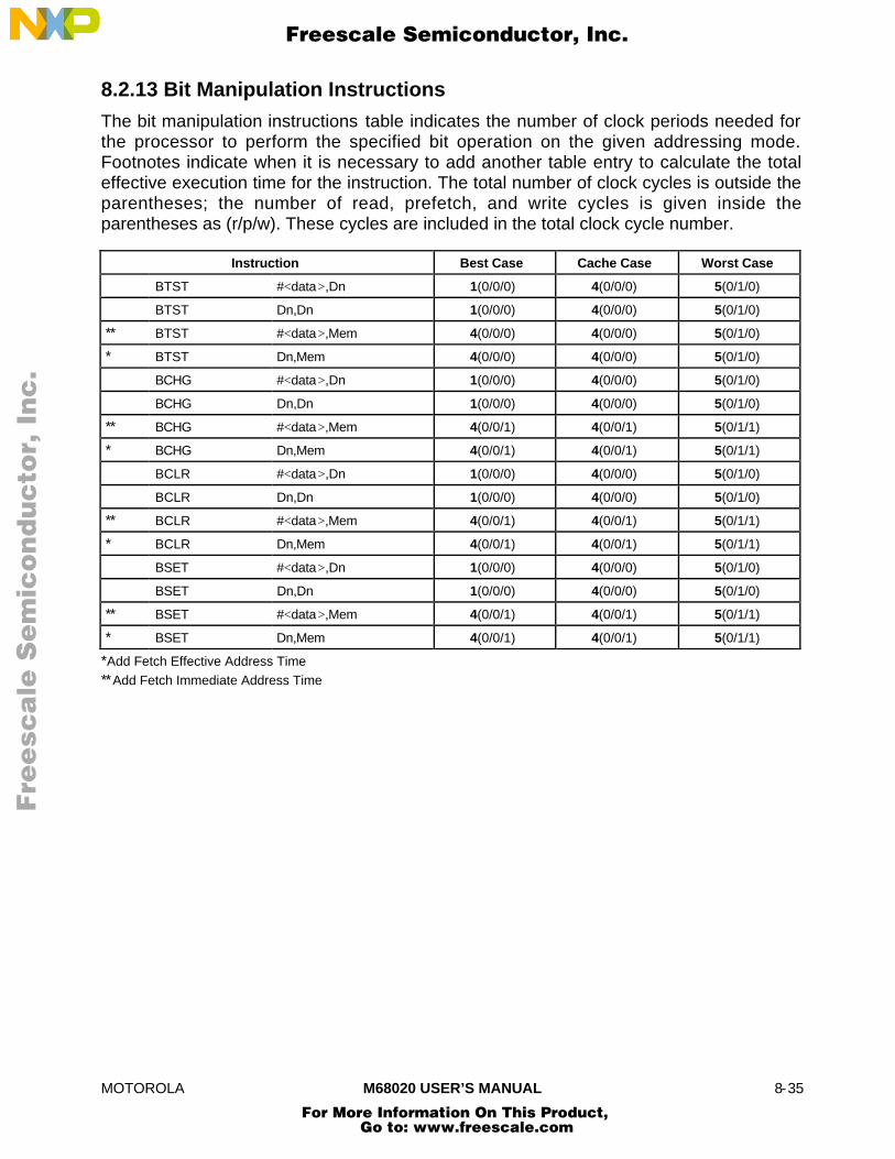
MOTOROLA M68020 USER’S MANUAL 8-35
8.2.13 Bit Manipulation Instructions
The bit manipulation instructions table indicates the number of clock periods needed forthe processor to perform the specified bit operation on the given addressing mode.Footnotes indicate when it is necessary to add another table entry to calculate the totaleffective execution time for the instruction. The total number of clock cycles is outside theparentheses; the number of read, prefetch, and write cycles is given inside theparentheses as (r/p/w). These cycles are included in the total clock cycle number.
Instruction Best Case Cache Case Worst Case
BTST #<data>,Dn 1(0/0/0) 4(0/0/0) 5(0/1/0)
BTST Dn,Dn 1(0/0/0) 4(0/0/0) 5(0/1/0)
** BTST #<data>,Mem 4(0/0/0) 4(0/0/0) 5(0/1/0)
* BTST Dn,Mem 4(0/0/0) 4(0/0/0) 5(0/1/0)
BCHG #<data>,Dn 1(0/0/0) 4(0/0/0) 5(0/1/0)
BCHG Dn,Dn 1(0/0/0) 4(0/0/0) 5(0/1/0)
** BCHG #<data>,Mem 4(0/0/1) 4(0/0/1) 5(0/1/1)
* BCHG Dn,Mem 4(0/0/1) 4(0/0/1) 5(0/1/1)
BCLR #<data>,Dn 1(0/0/0) 4(0/0/0) 5(0/1/0)
BCLR Dn,Dn 1(0/0/0) 4(0/0/0) 5(0/1/0)
** BCLR #<data>,Mem 4(0/0/1) 4(0/0/1) 5(0/1/1)
* BCLR Dn,Mem 4(0/0/1) 4(0/0/1) 5(0/1/1)
BSET #<data>,Dn 1(0/0/0) 4(0/0/0) 5(0/1/0)
BSET Dn,Dn 1(0/0/0) 4(0/0/0) 5(0/1/0)
** BSET #<data>,Mem 4(0/0/1) 4(0/0/1) 5(0/1/1)
* BSET Dn,Mem 4(0/0/1) 4(0/0/1) 5(0/1/1)
*Add Fetch Effective Address Time**Add Fetch Immediate Address Time
Fre
esc
ale
Se
mic
on
du
cto
r, I
Freescale Semiconductor, Inc.
For More Information On This Product, Go to: www.freescale.com
nc
...

8-36 M68020 USER’S MANUAL MOTOROLA
8.2.14 Bit Field Manipulation Instructions
The bit field manipulation instructions table indicates the number of clock periods neededfor the processor to perform the specified bit field operation using the given addressingmode. Footnotes indicate when it is necessary to add another table entry to calculate thetotal effective execution time for the instruction. The total number of clock cycles is outsidethe parentheses; the number of read, prefetch, and write cycles is given inside theparentheses as (r/p/w). These cycles are included in the total clock cycle number.
Instruction Best Case Cache Case Worst Case
BFTST Dn 3(0/0/0) 6(0/0/0) 7(0/1/0)
‡ BFTST Mem (< 5 Bytes) 11(1/0/0) 11(1/0/0) 12(1/1/0)
‡ BFTST Mem (5 Bytes) 15(2/0/0) 15(2/0/0) 16(2/1/0)
BFCHG Dn 9(0/0/0) 12(0/0/0) 12(0/1/0)
‡ BFCHG Mem (< 5 Bytes) 16(1/0/1) 16(1/0/1) 16(1/1/1)
‡ BFCHG Mem (5 Bytes) 24(2/0/2) 24(2/0/2) 24(2/1/2)
BFCLR Dn 9(0/0/0) 12(0/0/0) 12(0/1/0)
‡ BFCLR Mem (< 5 Bytes) 16(1/0/1) 16(1/0/1) 16(1/1/1)
‡ BFCLR Mem (5 Bytes) 24(2/0/2) 24(2/0/2) 24(2/1/2)
BFSET Dn 9(0/0/0) 12(0/0/0) 12(0/1/0)
‡ BFSET Mem (< 5 Bytes) 16(1/0/1) 16(1/0/1) 16(1/1/1)
‡ BFSET Mem (5 Bytes) 24(2/0/2) 24(2/0/2) 24(2/1/2)
BFEXTS Dn 5(0/0/0) 8(0/0/0) 8(0/1/0)
‡ BFEXTS Mem (< 5 Bytes) 13(1/0/0) 13(1/0/0) 13(1/1/0)
‡ BFEXTS Mem (5 Bytes) 18(2/0/0) 18(2/0/0) 18(2/1/0)
BFEXTU Dn 5(0/0/0) 8(0/0/0) 8(0/1/0)
‡ BFEXTU Mem (< 5 Bytes) 13(1/0/0) 13(1/0/0) 13(1/1/0)
‡ BFEXTU Mem (5 Bytes) 18(2/0/0) 18(2/0/0) 18(2/1/0)
BFINS Dn 7(0/0/0) 10(0/0/0) 10(0/1/0)
‡ BFINS Mem (< 5 Bytes) 14(1/0/1) 14(1/0/1) 15(1/1/1)
‡ BFINS Mem (5 Bytes) 20(2/0/2) 20(2/0/2) 21(2/1/2)
BFFFO Dn 15(0/0/0) 18(0/0/0) 18(0/1/0)
‡ BFFFO Mem (< 5 Bytes) 24(1/0/0) 24(1/0/0) 24(1/1/0)
‡ BFFFO Mem (5 Bytes) 32(2/0/0) 32(2/0/0) 32(2/1/0)
‡Add Calculate Immediate Address TimeNOTE: A bit field of 32 bits may span five bytes that require two operand cycles to access or may span four bytes that
require only one operand cycle to access.
Fre
esc
ale
Se
mic
on
du
cto
r, I
Freescale Semiconductor, Inc.
For More Information On This Product, Go to: www.freescale.com
nc
...
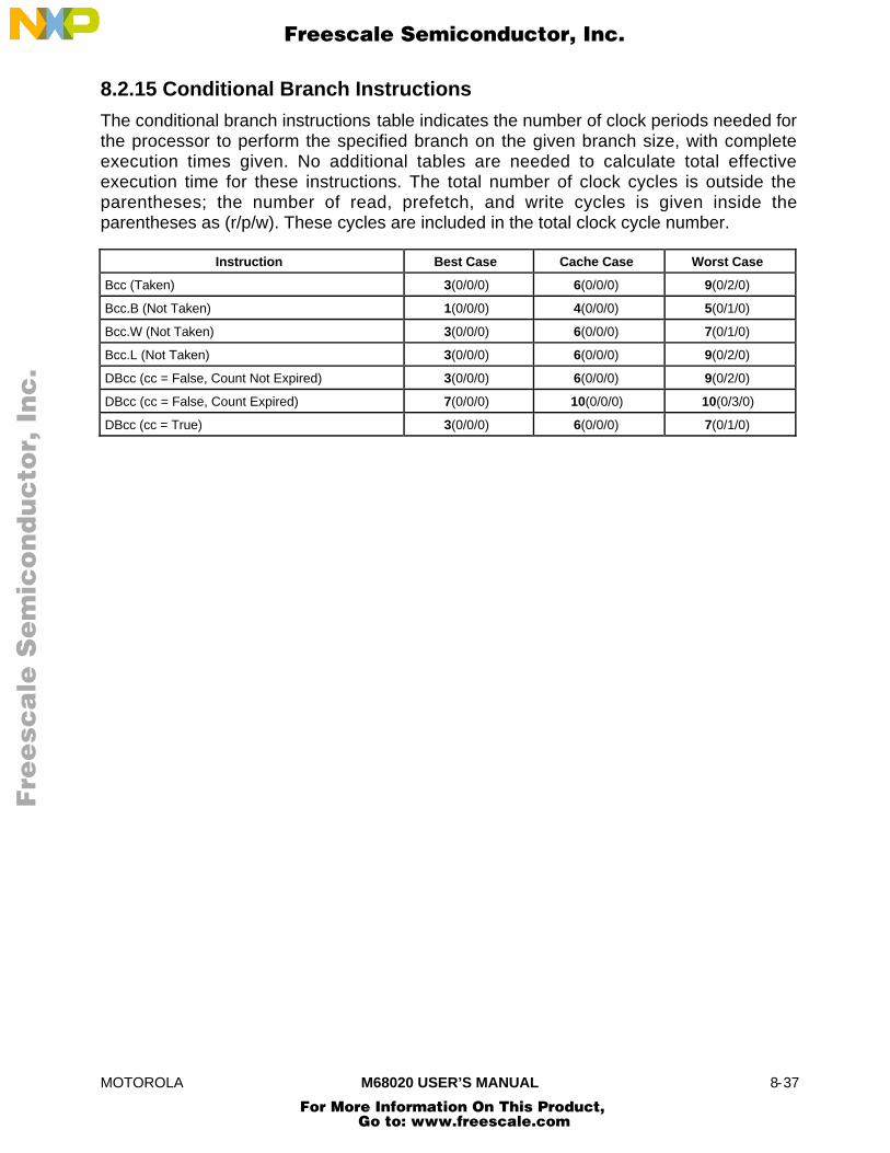
MOTOROLA M68020 USER’S MANUAL 8-37
8.2.15 Conditional Branch Instructions
The conditional branch instructions table indicates the number of clock periods needed forthe processor to perform the specified branch on the given branch size, with completeexecution times given. No additional tables are needed to calculate total effectiveexecution time for these instructions. The total number of clock cycles is outside theparentheses; the number of read, prefetch, and write cycles is given inside theparentheses as (r/p/w). These cycles are included in the total clock cycle number.
Instruction Best Case Cache Case Worst Case
Bcc (Taken) 3(0/0/0) 6(0/0/0) 9(0/2/0)
Bcc.B (Not Taken) 1(0/0/0) 4(0/0/0) 5(0/1/0)
Bcc.W (Not Taken) 3(0/0/0) 6(0/0/0) 7(0/1/0)
Bcc.L (Not Taken) 3(0/0/0) 6(0/0/0) 9(0/2/0)
DBcc (cc = False, Count Not Expired) 3(0/0/0) 6(0/0/0) 9(0/2/0)
DBcc (cc = False, Count Expired) 7(0/0/0) 10(0/0/0) 10(0/3/0)
DBcc (cc = True) 3(0/0/0) 6(0/0/0) 7(0/1/0)
Fre
esc
ale
Se
mic
on
du
cto
r, I
Freescale Semiconductor, Inc.
For More Information On This Product, Go to: www.freescale.com
nc
...

8-38 M68020 USER’S MANUAL MOTOROLA
8.2.16 Control Instructions
The control instructions table indicates the number of clock periods needed for theprocessor to perform the specified operation. Footnotes specify when it is necessary toadd an entry from another table to calculate the total effective execution time for the giveninstruction. The total number of clock cycles is outside the parentheses; the number ofread, prefetch, and write cycles is given inside the parentheses as (r/p/w). These cyclesare included in the total clock cycle number.
Instruction Best Case Cache Case Worst Case
ANDI to SR 9(0/0/0) 12(0/0/0) 15(0/2/0)
EORI to SR 9(0/0/0) 12(0/0/0) 15(0/2/0)
ORI to SR 9(0/0/0) 12(0/0/0) 15(0/2/0)
ANDI to CCR 9(0/0/0) 12(0/0/0) 15(0/2/0)
EORI to CCR 9(0/0/0) 12(0/0/0) 15(0/2/0)
ORI to CCR 9(0/0/0) 12(0/0/0) 15(0/2/0)
BSR 5(0/0/1) 7(0/0/1) 13(0/2/1)
** CALLM (Type 0) 28(2/0/6) 30(2/0/6) 36(2/2/6)
** CALLM (Type 1)—No Stack Copy 48(5/0/8) 50(5/0/8) 56(5/2/8)
** CALLM (Type 1)—No Stack Copy 55(6/0/8) 57(6/0/8) 64(6/2/8)
** CALLM (Type 1)—Stack Copy 63 + 6n (7 + n/0/8 + n) 65 + 6n (7 + n/0/8 + n) 71 + 6n (7 + n/2/8 + n)
‡ CAS (Successful Compare) 15(1/0/1) 15(1/0/1) 16(1/1/1)
‡ CAS (Unsuccessful Compare) 12(1/0/0) 12(1/0/0) 13(1/1/0)
CAS2 (Successful Compare) 23(2/0/2) 25(2/0/2) 28(2/2/2)
CAS2 (Unsuccessful Compare) 19(2/0/0) 22(2/0/0) 25(2/2/0)
* CHK 8(0/0/0) 8(0/0/0) 8(0/1/0)
** CHK2 EA,Rn 16(2/0/0) 18(2/0/0) 18(2/1/0)
% JMP 1(0/0/0) 4(0/0/0) 7(0/2/0)
% JSR 3(0/0/1) 5(0/0/1) 11(0/2/1)
† LEA 2(0/0/0) 2(0/0/0) 3(0/1/0)
LINK.W 3(0/0/1) 5(0/0/1) 7(0/1/1)
LINK.L 4(0/0/1) 6(0/0/1) 10(0/2/1)
NOP 2(0/0/0) 2(0/0/0) 3(0/1/0)
† PEA 3(0/0/1) 5(0/0/1) 6(0/1/1)
RTD 9(1/0/0) 10(1/0/0) 12(1/2/0)
RTM (Type 0) 18(4/0/0) 19(4/0/0) 22(4/2/0)
RTM (Type 1) 31(6/0/1) 32(6/0/1) 35(6/2/1)
RTR 13(2/0/0) 14(2/0/0) 15(2/2/0)
RTS 9(1/0/0) 10(1/0/0) 12(1/2/0)
UNLK 5(1/0/0) 6(1/0/0) 7(1/1/0)
n—Number of Operand Transfers Required %—Add Jump Effective Address Time*Add Fetch Effective Address Time **Add Fetch Immediate Address Time†Add Calculate Effective Address Time ‡Add Calculate Immediate Address Time
Fre
esc
ale
Se
mic
on
du
cto
r, I
Freescale Semiconductor, Inc.
For More Information On This Product, Go to: www.freescale.com
nc
...

MOTOROLA M68020 USER’S MANUAL 8-39
8.2.17 Exception-Related Instructions
The exception-related instructions table indicates the number of clock periods needed forthe processor to perform the specified exception-related action. Footnotes specify when itis necessary to add the entry from another table to calculate the total effective executiontime for the given instruction. The total number of clock cycles is outside the parentheses;the number of read, prefetch, and write cycles is given inside the parentheses as (r/p/w).These cycles are included in the total clock cycle number.
Instruction Best Case Cache Case Worst Case
BKPT 9(1/0/0) 10(1/0/0) 10(1/0/0)
Interrupt (I-Stack) 26(2/0/4) 26(2/0/4) 33(2/2/4)
Interrupt (M-Stack) 41(2/0/8) 41(2/0/8) 48(2/2/8)
RESET Instruction 518(0/0/0) 518(0/0/0) 519(0/1/0)
STOP 8(0/0/0) 8(0/0/0) 8(0/0/0)
Trace 25(1/0/5) 25(1/0/5) 32(1/2/5)
TRAP #n 20(1/0/4) 20(1/0/4) 27(1/2/4)
Illegal Instruction 20(1/0/4) 20(1/0/4) 27(1/2/4)
A-Line Trap 20(1/0/4) 20(1/0/4) 27(1/2/4)
F-Line Trap 20(1/0/4) 20(1/0/4) 27(1/2/4)
Privilege Violation 20(1/0/4) 20(1/0/4) 27(1/2/4)
TRAPcc (Trap) 23(1/0/5) 25(1/0/5) 32(1/2/5)
TRAPcc (No Trap) 1(0/0/0) 4(0/0/0) 5(0/1/0)
TRAPcc.W (Trap) 23(1/0/5) 25(1/0/5) 33(1/3/5)
TRAPcc.W (No Trap) 3(0/0/0) 6(0/0/0) 7(0/1/0)
TRAPcc.L (Trap) 23(1/0/5) 25(1/0/5) 33(1/3/5)
TRAPcc.L (No Trap) 5(0/0/0) 8(0/0/0) 10(0/2/0)
TRAPV (Trap) 23(1/0/5) 25(1/0/5) 32(1/2/5)
TRAPV (No Trap) 1(0/0/0) 4(0/0/0) 5(0/1/0)
Fre
esc
ale
Se
mic
on
du
cto
r, I
Freescale Semiconductor, Inc.
For More Information On This Product, Go to: www.freescale.com
nc
...
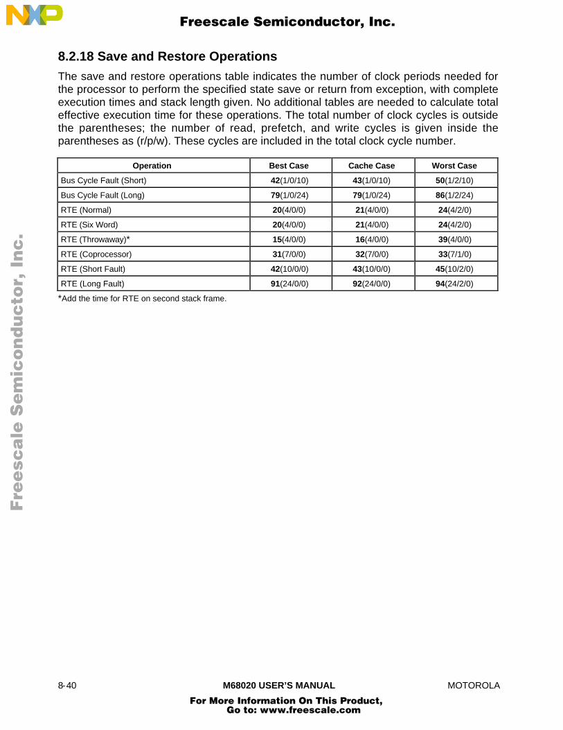
8-40 M68020 USER’S MANUAL MOTOROLA
8.2.18 Save and Restore Operations
The save and restore operations table indicates the number of clock periods needed forthe processor to perform the specified state save or return from exception, with completeexecution times and stack length given. No additional tables are needed to calculate totaleffective execution time for these operations. The total number of clock cycles is outsidethe parentheses; the number of read, prefetch, and write cycles is given inside theparentheses as (r/p/w). These cycles are included in the total clock cycle number.
Operation Best Case Cache Case Worst Case
Bus Cycle Fault (Short) 42(1/0/10) 43(1/0/10) 50(1/2/10)
Bus Cycle Fault (Long) 79(1/0/24) 79(1/0/24) 86(1/2/24)
RTE (Normal) 20(4/0/0) 21(4/0/0) 24(4/2/0)
RTE (Six Word) 20(4/0/0) 21(4/0/0) 24(4/2/0)
RTE (Throwaway)* 15(4/0/0) 16(4/0/0) 39(4/0/0)
RTE (Coprocessor) 31(7/0/0) 32(7/0/0) 33(7/1/0)
RTE (Short Fault) 42(10/0/0) 43(10/0/0) 45(10/2/0)
RTE (Long Fault) 91(24/0/0) 92(24/0/0) 94(24/2/0)
*Add the time for RTE on second stack frame.
Fre
esc
ale
Se
mic
on
du
cto
r, I
Freescale Semiconductor, Inc.
For More Information On This Product, Go to: www.freescale.com
nc
...
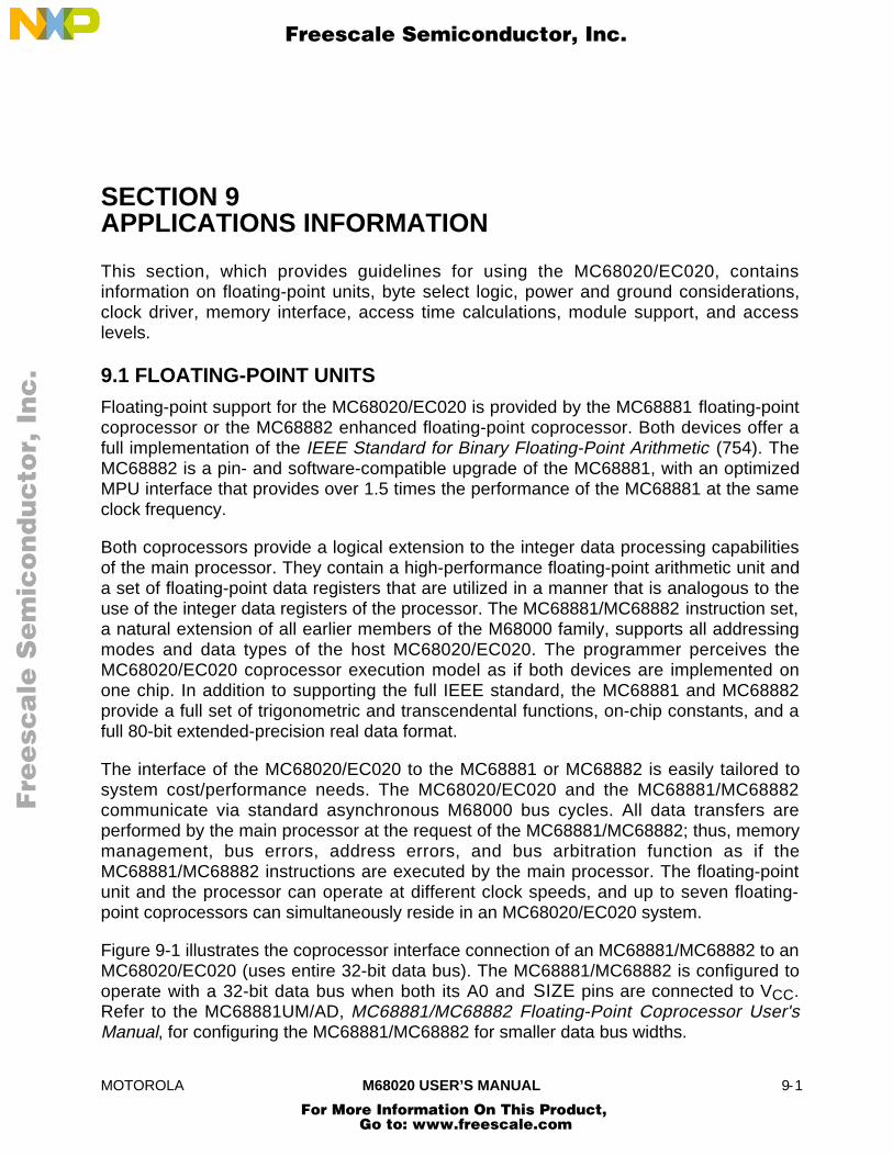
MOTOROLA M68020 USER’S MANUAL 9-1
SECTION 9APPLICATIONS INFORMATION
This section, which provides guidelines for using the MC68020/EC020, containsinformation on floating-point units, byte select logic, power and ground considerations,clock driver, memory interface, access time calculations, module support, and accesslevels.
9.1 FLOATING-POINT UNITS
Floating-point support for the MC68020/EC020 is provided by the MC68881 floating-pointcoprocessor or the MC68882 enhanced floating-point coprocessor. Both devices offer afull implementation of the IEEE Standard for Binary Floating-Point Arithmetic (754). TheMC68882 is a pin- and software-compatible upgrade of the MC68881, with an optimizedMPU interface that provides over 1.5 times the performance of the MC68881 at the sameclock frequency.
Both coprocessors provide a logical extension to the integer data processing capabilitiesof the main processor. They contain a high-performance floating-point arithmetic unit anda set of floating-point data registers that are utilized in a manner that is analogous to theuse of the integer data registers of the processor. The MC68881/MC68882 instruction set,a natural extension of all earlier members of the M68000 family, supports all addressingmodes and data types of the host MC68020/EC020. The programmer perceives theMC68020/EC020 coprocessor execution model as if both devices are implemented onone chip. In addition to supporting the full IEEE standard, the MC68881 and MC68882provide a full set of trigonometric and transcendental functions, on-chip constants, and afull 80-bit extended-precision real data format.
The interface of the MC68020/EC020 to the MC68881 or MC68882 is easily tailored tosystem cost/performance needs. The MC68020/EC020 and the MC68881/MC68882communicate via standard asynchronous M68000 bus cycles. All data transfers areperformed by the main processor at the request of the MC68881/MC68882; thus, memorymanagement, bus errors, address errors, and bus arbitration function as if theMC68881/MC68882 instructions are executed by the main processor. The floating-pointunit and the processor can operate at different clock speeds, and up to seven floating-point coprocessors can simultaneously reside in an MC68020/EC020 system.
Figure 9-1 illustrates the coprocessor interface connection of an MC68881/MC68882 to anMC68020/EC020 (uses entire 32-bit data bus). The MC68881/MC68882 is configured tooperate with a 32-bit data bus when both its A0 and SIZE pins are connected to VCC.Refer to the MC68881UM/AD, MC68881/MC68882 Floating-Point Coprocessor User'sManual, for configuring the MC68881/MC68882 for smaller data bus widths.
Fre
esc
ale
Se
mic
on
du
cto
r, I
Freescale Semiconductor, Inc.
For More Information On This Product, Go to: www.freescale.com
nc
...
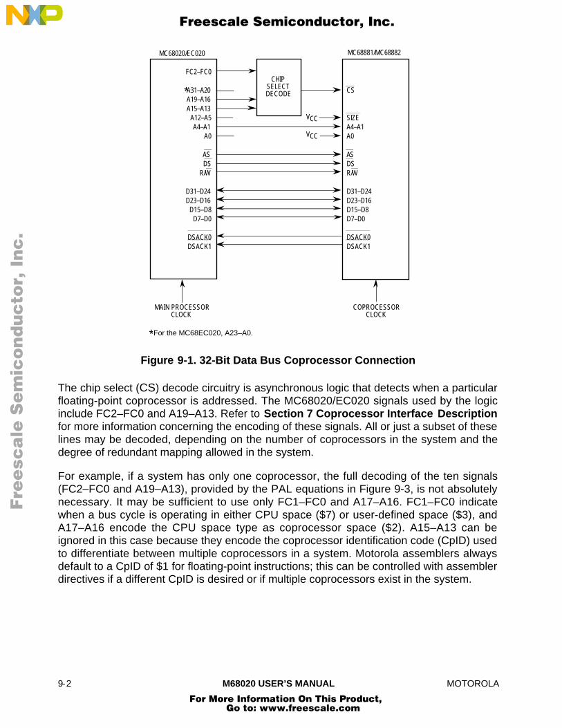
9-2 M68020 USER’S MANUAL MOTOROLA
MC68020/EC020 MC68881/MC68882
CHIPSELECTDECODE
FC2–FC0
A31–A20A19–A16A15–A13
A12–A5A4–A1
A0
ASDS
R/W
D31–D24D23–D16
D15–D8D7–D0
DSACK0DSACK1
MAIN PROCESSORCLOCK
CS
SIZEA4–A1A0
ASDSR/W
D31–D24D23–D16D15–D8D7–D0
DSACK0DSACK1
COPROCESSORCLOCK
VCC
VCC
*
*For the MC68EC020, A23–A0.
Figure 9-1. 32-Bit Data Bus Coprocessor Connection
The chip select (CS) decode circuitry is asynchronous logic that detects when a particularfloating-point coprocessor is addressed. The MC68020/EC020 signals used by the logicinclude FC2–FC0 and A19–A13. Refer to Section 7 Coprocessor Interface Descriptionfor more information concerning the encoding of these signals. All or just a subset of theselines may be decoded, depending on the number of coprocessors in the system and thedegree of redundant mapping allowed in the system.
For example, if a system has only one coprocessor, the full decoding of the ten signals(FC2–FC0 and A19–A13), provided by the PAL equations in Figure 9-3, is not absolutelynecessary. It may be sufficient to use only FC1–FC0 and A17–A16. FC1–FC0 indicatewhen a bus cycle is operating in either CPU space ($7) or user-defined space ($3), andA17–A16 encode the CPU space type as coprocessor space ($2). A15–A13 can beignored in this case because they encode the coprocessor identification code (CpID) usedto differentiate between multiple coprocessors in a system. Motorola assemblers alwaysdefault to a CpID of $1 for floating-point instructions; this can be controlled with assemblerdirectives if a different CpID is desired or if multiple coprocessors exist in the system.
Fre
esc
ale
Se
mic
on
du
cto
r, I
Freescale Semiconductor, Inc.
For More Information On This Product, Go to: www.freescale.com
nc
...

MOTOROLA M68020 USER’S MANUAL 9-3
The major concern of a system designer is to design a CS interface that meets the ACelectrical specifications for both the MC68020/EC020 (MPU) and the MC68881/MC68882(FPCP) without adding unnecessary wait states to FPCP accesses. The followingmaximum specifications (relative to CLK low) meet these objectives:
tCLK low to AS low ≤ (MPU Spec 1 – MPU Spec 47A – FPCP Spec 19) (9-1)
tCLK low to CS low ≤ (MPU Spec 1 – MPU Spec 47A – FPCP Spec 19) (9-2)
Even though requirement (9-1) is not met under worst-case conditions, if the MPU AS isloaded within specifications and the AS input to the FPCP is unbuffered, the requirementis met under typical conditions. Designing the CS generation circuit to meet requirement(9-2) provides the highest probability that accesses to the FPCP occur withoutunnecessary wait states. A PAL 16L8 (see Figure 9-2) with a maximum propagation delayof 10 ns, programmed according to the equations in Figure 9-3, can be used to generateCS. For a 25-MHz system, tCLK low to CS low is less than or equal to 10 ns when thisdesign is used. Should worst-case conditions cause tCLK low to AS low to exceedrequirement (1), one wait state is inserted in the access to the FPCP; no other adverseeffects occur. Figure 9-4 shows the bus cycle timing for this interface. Refer toMC68881UM/AD, MC68881/MC68882 Floating-Point Coprocessor User's Manual, forFPCP specifications.
The circuit that generates CS must meet another requirement. When a nonfloating-pointaccess immediately follows a floating-point access, CS (for the floating-point access) mustbe negated before AS and DS (for the subsequent access) are asserted. The PAL circuitpreviously described also meets this requirement.
PAL 16L810 ns
CLKAS
FC2
FC1FC0A19A18
A17A16
GND
VNCNC
NCNCA13A14
CLKDCSA15
CC
Figure 9-2. Chip Select Generation PAL
Fre
esc
ale
Se
mic
on
du
cto
r, I
Freescale Semiconductor, Inc.
For More Information On This Product, Go to: www.freescale.com
nc
...
9-4 M68020 USER’S MANUAL MOTOROLA
PAL16L8
FPCP CS GENERATION CIRCUITRY FOR 25 MHz OPERATION
MOTOROLA INC., AUSTIN, TEXAS
INPUTS: CLK ~AS FC2 FC1 FC0 A19 A18 A17 A16 A15 A14 A13
OUTPUTS: ~CS CLKD
!~CS = FC2 *FC1 *FC0 ;cpu space = $7
*!A19 *!A18 *A17 *!A16 ;coprocessor access = $2
*!A15 *!A14 *A13 ;coprocessor id = $1
*!CLK ;qualified by MPU clock low
+FC2 *FC1 *FC0 ;cpu space = $7
*!A19 *!A18 *A17 *!A16 ;coprocessor access = $2
*!A15 *!A14 *A13 ;coprocessor id = $1
*!~AS ;qualified by address strobe low
+FC2 *FC1 *FC0 ;cpu space = $7
*!A19 *!A18 *A17 *!A16 ;coprocessor access = $2
*!A15 *!A14 *A13 ;coprocessor id = $1
*CLKD ;qualified by CLKD (delayed CLK)
CLKD = CLK
Description: There are three terms to the CS generation. The first term denotes the earliest time CS can be asserted.The second term is used to assert CS until the end of the FPCP access. The third term is to ensure that no racecondition occurs in case of a late AS.
Figure 9-3. Chip Select PAL Equations
9
CLK
AS
CS
8
DSACK1/DSACK0
47A
START
19
FPCP SPECIFICATION MPU SPECIFICATION
Figure 9-4. Bus Cycle Timing Diagram
Fre
esc
ale
Se
mic
on
du
cto
r, I
Freescale Semiconductor, Inc.
For More Information On This Product, Go to: www.freescale.com
nc
...

MOTOROLA M68020 USER’S MANUAL 9-5
9.2 BYTE SELECT LOGIC FOR THE MC68020/EC020
The MC68020/EC020 architecture supports byte, word, and long-word operand transfersto any 8-, 16-, or 32-bit data port, regardless of alignment. This feature allows theprogrammer to write code that is not bus-width specific. When accessed, the peripheral ormemory subsystem reports its actual port size to the controller, and the MC68020/EC020then dynamically sizes the data transfer accordingly, using multiple bus cycles whennecessary. The following paragraphs describe the generation of byte select control signalsthat enable the dynamic bus sizing mechanism, the transfer of differently sized operands,and the transfer of misaligned operands to operate correctly.
The following signals control the MC68020/EC020 operand transfer mechanism:
A1, A0 — Address signals. The most significant byte of the operand to betransferred is addressed directly.
SIZ1, SIZ0 — Transfer size signals. Output of the MC68020/EC020. Theseindicate the number of bytes of an operand remaining to betransferred during a given bus cycle.
R/W — Read/Write signal. Output of the MC68020/EC020. For byteselect generation in MC68020/EC020 systems.
DSACK1, DSACK0 — Data transfer and size acknowledge signals. Driven by anasynchronous port to indicate the actual bus width ofthe port.
The MC68020/EC020 assumes that 16-bit ports are situated on data lines D31–D16, andthat 8-bit ports are situated on data lines D31–D24. This ensures that the following logicworks correctly with the MC68020/EC020's on-chip internal-to-external data busmultiplexer. Refer to Section 5 Bus Operation for more details on the dynamic bus sizingmechanism.
The need for byte select signals is best illustrated by an example. Consider a long-wordwrite cycle to an odd address in word-organized memory. The transfer requires three buscycles to complete. The first bus cycle transfers the most significant byte of the long wordon D23–D16. The second bus cycle transfers a word on D31–D16, and the last bus cycletransfers the least significant byte of the original long word on D31–D24. To preventoverwriting those bytes that are not used in these transfers, a unique byte data strobemust be generated for each byte when using devices with 16- and 32-bit port widths.
For noncachable read cycles and all write cycles, the required active bytes of the data busfor any given bus transfer are a function of the SIZ1, SIZ0 and A1, A0 outputs (see Table9-1). Individual strobes or select signals can be generated by decoding these four signalsfor every bus cycle. Devices residing on 8-bit ports can utilize DS or AS since there is onlyone valid byte for any transfer.
Fre
esc
ale
Se
mic
on
du
cto
r, I
Freescale Semiconductor, Inc.
For More Information On This Product, Go to: www.freescale.com
nc
...
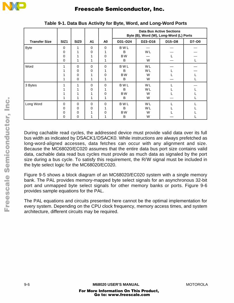
9-6 M68020 USER’S MANUAL MOTOROLA
Table 9-1. Data Bus Activity for Byte, Word, and Long-Word Ports
Data Bus Active SectionsByte (B), Word (W), Long-Word (L) Ports
Transfer Size SIZ1 SIZ0 A1 A0 D31–D24 D23–D16 D15–D8 D7–D0
Byte 0000
1111
0011
0101
B W LB
B WB
—W L—W
——L—
———L
Word 1111
0000
0011
0101
B W LB
B WB
W LW LWW
—LL—
——LL
3 Bytes 1111
1111
0011
0101
B W LB
B WB
W LW LWW
LLL—
—LLL
Long Word 0000
0000
0011
0101
B W LB
B WB
W LW LWW
LLL—
LLLL
During cachable read cycles, the addressed device must provide valid data over its fullbus width as indicated by DSACK1/DSACK0. While instructions are always prefetched aslong-word-aligned accesses, data fetches can occur with any alignment and size.Because the MC68020/EC020 assumes that the entire data bus port size contains validdata, cachable data read bus cycles must provide as much data as signaled by the portsize during a bus cycle. To satisfy this requirement, the R/W signal must be included inthe byte select logic for the MC68020/EC020.
Figure 9-5 shows a block diagram of an MC68020/EC020 system with a single memorybank. The PAL provides memory-mapped byte select signals for an asynchronous 32-bitport and unmapped byte select signals for other memory banks or ports. Figure 9-6provides sample equations for the PAL.
The PAL equations and circuits presented here cannot be the optimal implementation forevery system. Depending on the CPU clock frequency, memory access times, and systemarchitecture, different circuits may be required.
Fre
esc
ale
Se
mic
on
du
cto
r, I
Freescale Semiconductor, Inc.
For More Information On This Product, Go to: www.freescale.com
nc
...

MOTOROLA M68020 USER’S MANUAL 9-7
SIZ0SIZ1
A0A1
FC0FC1
A31–A2AS
R/W
D31–D0
UUDAUMDALMDALLDA
LLDBLMDBUMDBUUDB
MC68020/EC020 PAL16L8
D7–D0 D15–D8 D23–D16 D31–D24
W E W E W E W E
A31–A2
32-BIT PORT
UUDAUMDALMDALLDA
UNMAPPED BYTESELECTS FOR OTHER32-BIT PORTS
CPU
MC74F32MC74F32
MC74F32
MCM60256A MCM60256A MCM60256A MCM60256A
MC74F00
A21–A18MC74F32
*
*For the MC68EC020, A23–A2.
*
Figure 9-5. Example MC68020/EC020 Byte Select PAL System Configuration
Fre
esc
ale
Se
mic
on
du
cto
r, I
Freescale Semiconductor, Inc.
For More Information On This Product, Go to: www.freescale.com
nc
...

9-8 M68020 USER’S MANUAL MOTOROLA
PAL16L8
BYTE_SELECT
MC68020/EC020 BYTE DATA SELECT GENERATION FOR 32-BIT PORTS, MAPPED AND UNMAPPED.
MOTOROLA INC., AUSTIN, TEXAS
INPUTS: A0 A1 SIZ0 SIZ1 RW A18 A19 A20 A21 ~CPU
OUTPUTS: ~UUDA ~UMDA ~LMDA ~LLDA ~UUDA ~UMDB ~LMDB ~LLDB
!~UUDA = RW ;enable upper byte on read of 32-bit port
+!A0 *!A1 ;directly addressed, any size
!~UMDA = RW ;enable upper middle byte on read of 32-bit port
+A0 *!A1 ;directly addressed, any size
+!A1 *!SIZ0 ;even word aligned, size word or long word
+!A1 *SIZ1 ;even word aligned, size is word or three byte
!~LMDA = RW ;enable lower middle byte on read of 32-bit port +!A0 *A1;directly addressed, any size
+!A1 *!SIZ0 *!SIZ1 ;even word aligned, size is long word
+!A1 *SIZ0 *SIZ1 ;even word aligned, size is three byte
+!A1 *A0 *!SIZ0 ;even word aligned, size is word or long word
!~LLDA = RW ;enable lower byte on read of 32-bit port
+A0 *A1 ;directly addressed, any size
+A0 *SIZ0 *SIZ1 ;odd byte alignment, three byte size
+!SIZ0 *!SIZ1 ;size is long word, any address
+A1 *SIZ1 ;odd word aligned, word or three byte size
!~UUDB = RW *!~CPU * (addressb) ;enable upper byte on read of 32-bit port
+!A0 *!A1 *!~CPU * (addressb) ;directly addressed, any size
!~UMDB = RW *!~CPU * (addressb) ;enable upper middle byte on read of 32-bit port
+ A0 *!A1 *!~CPU * (addressb) ;directly addressed, any size
+!A1 *!SIZ0 *!~CPU * (addressb) ;even word aligned, size word or long word
+!A1 *SIZ1 *!~CPU * (addressb) ;even word aligned, size is word or three byte
!~LMDB =RW *!~CPU * (addressb) ;enable lower middle byte on read of 32-bit port
+!A0 * A1 *!~CPU * (addressb) ;directly addressed, any size
+!A1 *!SIZ0 *!SIZ1 *!~CPU * (addressb) ;even word aligned, size is long word
+!A1 * SIZ0 * SIZ1 *!~CPU * (addressb) ;even word aligned, size is three byte
+!A1 * A0 *!SIZ0 *!~CPU * (addressb) ;even word aligned, size is word or long word
!~LLDB =RW *!~CPU * (addressb) ;enable lower byte on read of 32-bit port
+A0 * A1 *!~CPU * (addressb) ;directly addressed, any size
+ A0 * SIZ0 * SIZ1 *!~CPU * (addressb) ;odd byte alignment, three byte size
+!SIZ0 *!SIZ1 *!~CPU * (addressb) ;size is long word, any address
+A1 * SIZ1 *!~CPU * (addressb) ;odd word aligned, word or three byte size
DESCRIPTION: Byte select signals for writing. On reads, all byte selects are asserted if the respective memory block is addressed.The input signal CPU prevents byte select assertion during CPU space cycles and is derived from NANDing FC1–FC0 or FC2–FC0.The label (addressb) is a designer-selectable combination of address lines used to generate the proper address decode for thesystem's memory bank. With the address lines given here, the decode block size is 256 Kbytes to 2 Mbytes. A similar address mightbe included in the equations for UUDA, UMDA, etc. if the designer wishes them to be memory mapped also.
Figure 9-6. MC68020/EC020 Byte Select PAL Equations
Fre
esc
ale
Se
mic
on
du
cto
r, I
Freescale Semiconductor, Inc.
For More Information On This Product, Go to: www.freescale.com
nc
...
MOTOROLA M68020 USER’S MANUAL 9-9
9.3 POWER AND GROUND CONSIDERATIONS
The MC68020/EC020 is fabricated in Motorola's advanced HCMOS process and iscapable of operating at clock frequencies of up to 25 MHz. While the use of CMOS for adevice containing such a large number of transistors allows significantly reduced powerconsumption compared to an equivalent NMOS circuit, the high clock speed makes thecharacteristics of power supplied to the device very important. The power supply must beable to furnish large amounts of instantaneous current when the MC68020/EC020performs certain operations, and it must remain within the rated specification at all times.To meet these requirements, more detailed attention must be given to the power supplyconnection to the MC68020/EC020 than is required for NMOS devices operating at slowerclock rates.
To reduce the amount of noise in the power supply connected to the MC68020/EC020and to provide for the instantaneous current requirements, common capacitive decouplingtechniques should be observed. While there is no recommended layout for this capacitivedecoupling, it is essential that the inductance and distance between these devices and theMC68020/EC020 be minimized to provide sufficiently fast response time to satisfymomentary current demands and to maintain a constant supply voltage. It is suggestedthat high-frequency, high-quality capacitors be placed as close to the MC68020/EC020 aspossible. Table 9-2 lists the VCC and GND pin assignments for the MC68EC020 PPGA(RP suffix) package. Table 9-3 lists the VCC and GND pin assignments for theMC68EC020 PQFP (FG suffix) package. Refer to Section 11 Ordering Information andMechanical Data for the VCC and GND pin assignments for the MC68020 packages.When assigning capacitors to the VCC and GND pins, the noisier pins (address and databuses) should be heavily decoupled from the internal logic pins. Typical decouplingpractices include a high-frequency, high-quality capacitor to decouple every device on theprinted circuit board; however, due to the power requirements and drive capability of theMC68020/EC020, each VCC pin should be decoupled with an individual capacitor.Motorola recommends using a capacitor in the range of 0.01 µF to 0.1 µF on each VCCpin on each device to provide filtering for most frequencies prevalent in a digital system. Inaddition to the individual decoupling, several bulk decoupling capacitors should be placedonto the printed circuit board with typical values in the range of 33 µF to 330 µF. Whenpower and ground planes are used with an adequate number of high-frequency, high-quality capacitors, the system noise will be reduced to the required levels, and theMC68020/EC020 will function properly. Similar decoupling techniques should also beobserved for other VLSI devices in the system.
In addition to the capacitive decoupling of the power supply, care must be taken to ensurea low-impedance connection between all MC68020/EC020 VCC and GND pins and thesystem power supply. A solid power supply connection from the power and ground planesto the MC68020/EC020 VCC and GND pins, respectively, will meet this requirement.Failure to provide connections of sufficient quality between the MC68020/EC020 powerpins and the system power supplies will result in increased assertion delays for externalsignals, decreased voltage noise margins, increased system noise, and possible errors inMC68020/EC020 internal logic.
Fre
esc
ale
Se
mic
on
du
cto
r, I
Freescale Semiconductor, Inc.
For More Information On This Product, Go to: www.freescale.com
nc
...
9-10 M68020 USER’S MANUAL MOTOROLA
Table 9-2. VCC and GND Pin Assignments—MC68EC020 PPGA (RP Suffix)
Pin Group VCC GND
Address Bus B7, C7 A1, A7, C8, D13
Data Bus K12, M9, N9 J13, L8, M1, M8
Internal Logic D1, D2, E12, E13 F11, F12, J1, J2
Clock — B1
Table 9-3. VCC and GND Pin Assignments—MC68EC020 PQFP (FG Suffix)
Pin Group VCC GND
Address Bus 90 72, 89, 100
Data Bus 44, 57 26, 43, 58, 59
Internal Logic 7, 8, 70, 71 3, 20, 21, 68, 69
Clock — 4
9.4 CLOCK DRIVER
The MC68020/EC020 is designed to sustain high performance while using low-costmemory subsystems. The MC68020/EC020 requires a stable clock source that is free ofringing and ground bounce, has sufficient rise and fall times, and meets the minimum andmaximum high and low cycle times. The individual system may require additional clocksfor peripherals with a minimum amount of clock skew. Two possible clock solutions areprovided with the MC88916 and MC74F803. Many other clock solutions can be used.Some crystal clock drivers are capable of driving the MC68020/EC020 directly. For slowerspeed designs, a simple 74F74 flip-flop meets the clocking needs of the MC68020/EC020.Coupled with the MC88916 or MC74F803 clock generation and distribution circuit, theMC68020/EC020 provides simple interface to lower speed memory subsystems. TheMC88916 (see Figure 9-7) and MC74F803 (see Figure 9-8) generate the clock signalsrequired to minimize the skew between different clocks to multiple devices such ascoprocessors, synchronous state machines, DRAM controllers, and memory subsystems.The MC88916 clock driver can be used in doubling and synchronizing a low-frequencyclock source. The MC74F803 will provide a controlled skew output for clocking otherperipherals.
Fre
esc
ale
Se
mic
on
du
cto
r, I
Freescale Semiconductor, Inc.
For More Information On This Product, Go to: www.freescale.com
nc
...

MOTOROLA M68020 USER’S MANUAL 9-11
MC68020/EC02025 MHz
12.5-MHzOSCILLATOR
CONTROLLERCLOCK (25 MHz)
BUS CLOCKS(25 MHz)
MC88916
CLOCK(50 MHz)
12.5 MHz
2
CLOCK(25 MHz)
Figure 9-7. High-Resolution Clock Controller
MC68020/EC02025 MHz
50-MHzOSCILLATOR
CONTROLLERCLOCK (25 MHz)
BUS CLOCKS(25 MHz)
MC74F803
CLOCK(25 MHz)
2
Figure 9-8. Alternate Clock Solution
9.5 MEMORY INTERFACE
The MC68020/EC020 is capable of running an external bus cycle in a minimum of threeclocks (refer to Section 5 Bus Operation). The MC68020/EC020 runs an asynchronousbus cycle, terminated by the DSACK1/DSACK0 signals, and has a minimum duration ofthree controller clock periods in which up to four bytes (32 bits) are transferred.
During read operations, the MC68020/EC020 latches data on the last falling clock edge ofthe bus cycle, one-half clock before the bus cycle ends. Latching data here, instead of thenext rising clock edge, helps to avoid data bus contention with the next bus cycle andallows the MC68020/EC020 to receive the data into its execution unit sooner for a netperformance increase.
Write operations also use this data bus timing to allow data hold times from the negatingstrobes and to avoid any bus contention with the following bus cycle. ThisMC68020/EC020 characteristic allows the system to be designed with a minimum of busbuffers and latches.
One benefit of the MC68020/EC020 on-chip instruction cache is that the effect of externalwait states on performance is lessened because the caches are always accessed in fewerthan “no wait states,” regardless of the external memory configuration.
Fre
esc
ale
Se
mic
on
du
cto
r, I
Freescale Semiconductor, Inc.
For More Information On This Product, Go to: www.freescale.com
nc
...
9-12 M68020 USER’S MANUAL MOTOROLA
9.6 ACCESS TIME CALCULATIONS
The timing paths that are critical in any memory interface are illustrated and defined inFigure 9-9.
The type of device that is interfaced to the MC68020/EC020 determines exactly which ofthe paths is most critical. The address-to-data paths are typically the critical paths forstatic devices since there is no penalty for initiating a cycle to these devices and latervalidating that access with the appropriate bus control signal. Conversely, the address-strobe-to-data-valid path is often most critical for dynamic devices since the cycle must bevalidated before an access can be initiated. For devices that signal termination of a buscycle before data is validated (e.g., error detection and correction hardware and someexternal caches), to improve performance, the critical path may be from the address orstrobes to the assertion of BERR (or BERR and HALT). Finally, the address-valid-to-DSACK1/DSACK0-asserted path is most critical for very fast devices and externalcaches, since the time available between the address becoming valid and theDSACK1/DSACK0 assertion to terminate the bus cycle is minimal. Table 9-4 providesthe equations required to calculate the various memory access times assuming a 50-percent duty cycle clock.
CLK
A31–A0
S0 S1 S2 S0
AS
DSACK1/DSACK0
a c e
b d f
BERR, HALT
D31–D0
NOTE: This diagram illustrates access time calculations only
*
*For the MC68EC020, A23–A0.
Parameter Description System Equationa Address Valid to DSACK1/DSACK0 Asserted tAVDL 9-3
b AS Asserted to DSACK1/DSACK0 Asserted tSADL 9-4
c Address Valid to BERR/HALT Asserted tAVBHL 9-5
d AS Asserted to BERR/HALT Asserted tSABHL 9-6
e Address Valid to Data Valid tAVDV 9-7f AS Asserted to Data Valid tSADV 9-8
Fre
esc
ale
Se
mic
on
du
cto
r, I
Freescale Semiconductor, Inc.
For More Information On This Product, Go to: www.freescale.com
nc
...

MOTOROLA M68020 USER’S MANUAL 9-13
Figure 9-9. Access Time Computation Diagram
Fre
esc
ale
Se
mic
on
du
cto
r, I
Freescale Semiconductor, Inc.
For More Information On This Product, Go to: www.freescale.com
nc
...

9-14 M68020 USER’S MANUAL MOTOROLA
Table 9-4. Memory Access Time Equations at 16.67 and 25 MHz
Equation 16.667 MHz N = 3 N = 4 N = 5 N = 6 N = 7 Unit
9-3 tAVDL = (N – 1) • t1 – t2 – t6 – t47A 61 121 181 241 301 ns
9-4 tSADL = (N – 1) • t1 – t9 – t60 25 85 145 205 265 ns
9-5 tAVBHL = N • t1 – t2 – t6 – t27A 22 46 70 94 118 ns
9-6 tSABHL = (N – 1) • t1 – t9 – t27A 40 70 100 130 160 ns
9-7 tAVDV = N • t1 – t2 – t6 – t27 121 181 241 301 361 ns
9-8 tSADV = (N – 1) • t1 – t9 – t27 85 145 205 265 325 ns
Equation 25 MHz N = 3 N = 4 N = 5 N = 6 N = 7 Unit
9-3 tAVDL = (N – 1) • t1 – t2 – t6 – t47A 31 71 111 151 191 ns
9-4 tSADL = (N – 1) • t1 – t9 – t60 17 57 97 137 177 ns
9-5 tAVBHL = N • t1 – t2 – t6 – t27A 22 41 60 79 98 ns
9-6 tSABHL = (N – 1) • t1 – t9 – t27A 26 44 62 80 98 ns
9-7 tAVDV = N • t1 – t2 – t6 – t27 71 111 151 191 231 ns
9-8 tSADV = (N – 1) • t1 – t9 – t27 57 97 137 177 217 ns
Where:tX = Refers to AC Electrical Specification Xt1 = The Clock Periodt2 = The Clock Low Timet3 = The Clock High Timet6 = The Clock High to Address Valid Timet9 = The Clock Low to AS Low Delay
t27 = The Data-In to Clock Low Setup Timet27A = The BERR/HALT to Clock Low Setup Timet47A = The Asynchronous Input Setup Time
N = The Total Number of Clock Periods in the Bus Cycle (N ≥ 3 Cycles)
During asynchronous bus cycles, DSACK1/DSACK0 are used to terminate the currentbus cycle. In true asynchronous operations, such as accesses to peripherals operating ata different clock frequency, either or both signals may be asserted without regard to theclock, and then data must be valid a certain amount of time later as defined byspecification 31. With a 25-MHz controller, this time is 32 ns after DSACK1/DSACK0asserts; with a 16.67-MHz controller, this time is 50 ns after DSACK1/DSACK0 asserts(both numbers vary with the actual clock frequency).
However, many local memory systems do not operate in a truly asynchronous mannerbecause either the memory control logic can be related to the MC68020/EC020 clock orworst-case propagation delays are known; thus, asynchronous setup times for theDSACK1/DSACK0 signals can be guaranteed. The timing requirements for this pseudo-synchronous DSACK1/DSACK0 generation is governed by the equation for tAVDL.
Fre
esc
ale
Se
mic
on
du
cto
r, I
Freescale Semiconductor, Inc.
For More Information On This Product, Go to: www.freescale.com
nc
...
MOTOROLA M68020 USER’S MANUAL 9-15
Another way to optimize the CPU-to-memory access times in a system is to use a clockfrequency less than the rated maximum of the specific MC68020/EC020 device. Table 9-5provides calculated tAVDV (see Equation 9-7 of Table 9-4) results for a 16 MHzMC68020/EC020 and a 25 MHz MC68020/EC020 operating at various clock frequencies.If the system uses other clock frequencies, the above equations can be used to calculatethe exact access times.
Table 9-5. Calculated tAVDV Values for Operation at FrequenciesLess Than or Equal to the CPU Maximum Frequency Rating
Equation 9-7 tAVDV 16-MHz MC68020/EC020 25-MHz MC68020/EC020
Clocks Per (N) and TypeBus Cycle
WaitStates
Clock at12.5 MHz
Clock at16.67 MHz
Clock at16.67 MHz
Clock at20 MHz
Clock at25 MHz
3 Clock Asynchronous 0 181 121 131 101 71
4 Clock Asynchronous 1 261 181 191 151 111
5 Clock Asynchronous 2 341 241 251 201 151
6 Clock Asynchronous 3 421 301 311 251 191
9.7 MODULE SUPPORT
The MC68020/EC020 includes support for modules with the CALLM and RTMinstructions. The CALLM instruction references a module descriptor. This descriptorcontains control information for entry into the called module. The CALLM instructioncreates a module stack frame and stores the current module state in that frame and loadsa new module state from the referenced descriptor. The RTM instruction recovers theprevious module state from the stack frame and returns to the calling module.
The module interface facilitates finer resolution of access control by external hardware.Although the MC68020/EC020 does not interpret the access control information, itcommunicates with external hardware when the access control is to be changed andrelies on the external hardware to verify that the changes are legal.
9.7.1 Module Descriptor
Figure 9-10 illustrates the format of the module descriptor. The first long word containscontrol information used during execution of the CALLM instruction. The remaininglocations contain data that can be loaded into processor registers by the CALLMinstruction.
Fre
esc
ale
Se
mic
on
du
cto
r, I
Freescale Semiconductor, Inc.
For More Information On This Product, Go to: www.freescale.com
nc
...

9-16 M68020 USER’S MANUAL MOTOROLA
OPT TYPE ACCESS LEVEL (RESERVED, MUST BE ZERO)
31 28 23 15 0
BASE+$04
MODULE ENTRY WORD POINTER
MODULE DATA AREA POINTER
ADDITIONAL USER-DEFINED INFORMATION
+$08
+$0C
+$10
29 24 16
Figure 9-10. Module Descriptor Format
The opt field specifies how arguments are to be passed to the called module; theMC68020/EC020 recognizes only the options of 000 and 100; all others cause a formatexception. The 000 option indicates that the called module expects to find arguments fromthe calling module on the stack just below the module stack frame. In cases where there isa change of stack pointer during the call, the MC68020/EC020 will copy the argumentsfrom the old stack to the new stack. The 100 option indicates that the called module willaccess the arguments from the calling module through an indirect pointer in the stack ofthe calling module. Hence, the arguments are not copied, but the MC68020/EC020 putsthe value of the stack pointer from the calling module in the module stack frame.
The type field specifies the type of the descriptor; the MC68020/EC020 only recognizesdescriptors of type $00 and $01; all others cause a format exception. The $00 typedescriptor defines a module for which there is no change in access rights, and the calledmodule builds its stack frame on top of the stack used by the calling module. The $01 typedescriptor defines a module for which there may be a change in access rights; such acalled module may have a separate stack area from that of the calling module.
The access level field is used only with the type $01 descriptor and is passed to externalhardware to change the access control.
The module entry word pointer specifies the entry address of the called module. The firstword at the entry address (see Figure 9-11) specifies the register to be saved in themodule stack frame and then loaded with the module descriptor data area pointer; the firstinstruction of the module starts with the next word. The module descriptor data areapointer field contains the address of the called module data area.
If the access change requires a change of stack pointer, the old value is saved in themodule stack frame, and the new value is taken from the module descriptor stack pointerfield. Any further information in the module descriptor is user defined.
OPERATION WORD OF FIRST INSTRUCTION
D/A
15 14
REGISTER
12 11 9
0
8
0
7
0
6 5 0
0 0
4
0
3
0
2
0
1
000
10
0
Figure 9-11. Module Entry Word
Fre
esc
ale
Se
mic
on
du
cto
r, I
Freescale Semiconductor, Inc.
For More Information On This Product, Go to: www.freescale.com
nc
...
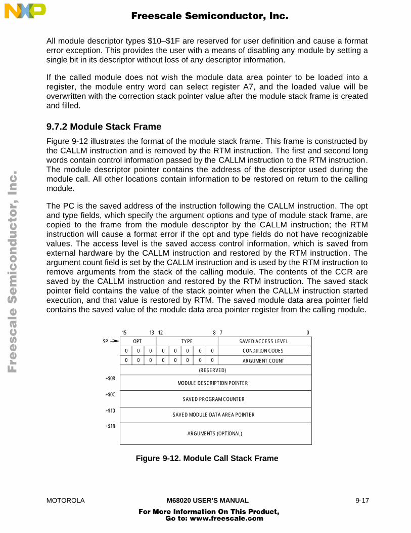
MOTOROLA M68020 USER’S MANUAL 9-17
All module descriptor types $10–$1F are reserved for user definition and cause a formaterror exception. This provides the user with a means of disabling any module by setting asingle bit in its descriptor without loss of any descriptor information.
If the called module does not wish the module data area pointer to be loaded into aregister, the module entry word can select register A7, and the loaded value will beoverwritten with the correction stack pointer value after the module stack frame is createdand filled.
9.7.2 Module Stack Frame
Figure 9-12 illustrates the format of the module stack frame. This frame is constructed bythe CALLM instruction and is removed by the RTM instruction. The first and second longwords contain control information passed by the CALLM instruction to the RTM instruction.The module descriptor pointer contains the address of the descriptor used during themodule call. All other locations contain information to be restored on return to the callingmodule.
The PC is the saved address of the instruction following the CALLM instruction. The optand type fields, which specify the argument options and type of module stack frame, arecopied to the frame from the module descriptor by the CALLM instruction; the RTMinstruction will cause a format error if the opt and type fields do not have recognizablevalues. The access level is the saved access control information, which is saved fromexternal hardware by the CALLM instruction and restored by the RTM instruction. Theargument count field is set by the CALLM instruction and is used by the RTM instruction toremove arguments from the stack of the calling module. The contents of the CCR aresaved by the CALLM instruction and restored by the RTM instruction. The saved stackpointer field contains the value of the stack pointer when the CALLM instruction startedexecution, and that value is restored by RTM. The saved module data area pointer fieldcontains the saved value of the module data area pointer register from the calling module.
TYPE SAVED ACCESS LEVEL
15 12 7 0
SP
+$08
SAVED PROGRAM COUNTER
SAVED MODULE DATA AREA POINTER
ARGUMENTS (OPTIONAL)
+$0C
+$10
MODULE DESCRIPTION POINTER
(RESERVED)
CONDITION CODES
ARGUMENT COUNT
OPT
0 0 0
0 0 0
0 0 0
0 0 0
0 0
0 0
+$18
13 8
Figure 9-12. Module Call Stack Frame
Fre
esc
ale
Se
mic
on
du
cto
r, I
Freescale Semiconductor, Inc.
For More Information On This Product, Go to: www.freescale.com
nc
...

9-18 M68020 USER’S MANUAL MOTOROLA
9.8 ACCESS LEVELS
The MC68020/EC020 module mechanism supports a finer level of access control beyondthe distinction between user and supervisor privilege levels. The module mechanismallows a module with limited access rights to call a module with greater access rights. Withthe help of external hardware, the processor can verify that an increase in access rights isallowable or can detect attempts by a module to gain access rights to which it is notentitled.
Type $01 module descriptors and module stack frames indicate a request to changeaccess levels. While processing a type $01 descriptor or frame, the CALLM and RTMinstructions communicate with external access control hardware via accesses in the CPUspace. For these accesses, A19–A16 equal 0001. Figure 9-13 shows the address map forthese CPU space accesses. If the processor receives a bus error on any of these CPUspace accesses during the execution of a CALLM or RTM instruction, the processor willtake a format error exception.
31 0
CAL
23
DAL
24
ACCESS STATUS REGISTER
IAL
$00
$04
$08
$0C
$40
$44
$48
$4C
$50
$54
$58
$5C
(UNUSED, RESERVED)
(UNUSED, RESERVED)
(UNUSED, RESERVED)
(UNUSED, RESERVED)
FUNCTION CODE 5 DESCRIPTOR ADDRESS (SUPERVISOR PROGRAM)
FUNCTION CODE 6 DESCRIPTOR ADDRESS
FUNCTION CODE 7 DESCRIPTOR ADDRESS (CPU SPACE)
FUNCTION CODE 4 DESCRIPTOR ADDRESS (SUPERVISOR DATA)
FUNCTION CODE 3 DESCRIPTOR ADDRESS
FUNCTION CODE 2 DESCRIPTOR ADDRESS (USER PROGRAM)
FUNCTION CODE 1 DESCRIPTOR ADDRESS (USER DATA)
FUNCTION CODE 0 DESCRIPTOR ADDRESS
Figure 9-13. Access Level Control Bus Registers
The current access level register (CAL) contains the access level rights of the currentlyexecuting module. The increase access level register (IAL) is the register through whichthe processor requests increased access rights. The decrease access level register (DAL)is the register through which the processor requests decreased access rights. The formatsof these three registers are undefined to the main processor, but the main processorassumes that information read from the module descriptor stack frame or the CAL can bemeaningfully written to the IAL or the DAL. The access status register allows theprocessor to query the external hardware as to the legality of intended access leveltransitions. Table 9-6 lists the valid values of the access status register.
Fre
esc
ale
Se
mic
on
du
cto
r, I
Freescale Semiconductor, Inc.
For More Information On This Product, Go to: www.freescale.com
nc
...

MOTOROLA M68020 USER’S MANUAL 9-19
Table 9-6. Access Status Register Codes
Value Validity Processor Action
$00 Invalid Format Error
$01 Valid No Change in Access Rights
$02–$03 Valid Change Access Rights with No Change of Stack Pointer
$04–$07 Valid Change Access Rights and Change Stack Pointer
Other Undefined Undefined (Take Format Error Exception)
The processor uses the descriptor address registers during the CALLM instruction tocommunicate the address of the type $01 descriptor, allowing external hardware to verifythat the address is a valid address for a type $01 descriptor. This validation prevents amodule from creating a type $01 descriptor to increase its access rights.
9.8.1 Module Call
The CALLM instruction is used to make the module call. For the type $00 moduledescriptor, the processor creates and fills the module stack frame at the top of the activesystem stack. The condition codes of the calling module are saved in the CCR field of theframe. If opt is equal to 000 (arguments passed on the stack) in the module descriptor, theMC68020/EC020 does not save the stack pointer or load a new stack pointer value. Theprocessor uses the module entry word to save and load the module data area pointerregister and then begins execution of the called module.
For the type $01 module descriptor, the processor must first obtain the current accesslevel from external hardware. It also verifies that the calling module has the right to readfrom the area pointed to by the current value of the stack pointer by reading from thataddress. It passes the descriptor address and increase access level to external hardwarefor validation and then reads the access status. If external hardware determines that thechange in access rights should not be granted, the access status is zero, and theprocessor takes a format error exception. No visible processor registers are changed, norshould the current access level enforced by external hardware be changed. If externalhardware determines that a change should be granted, the external hardware changes itsaccess level, and the processor proceeds. If the access status register indicates that achange in the stack pointer is required, the stack pointer is saved internally, a new value isloaded from the module descriptor, and arguments are copied from the calling stack to thenew stack. Finally, the module stack frame is created and filled on the top of the currentstack. The condition codes of the calling module are saved in the CCR field of the frame.Execution of the called module then begins as with a type $00 descriptor.
Fre
esc
ale
Se
mic
on
du
cto
r, I
Freescale Semiconductor, Inc.
For More Information On This Product, Go to: www.freescale.com
nc
...

9-20 M68020 USER’S MANUAL MOTOROLA
9.8.2 Module Return
The RTM instruction is used to return from a module. For the type $00 module stackframe, the processor reloads the condition codes, the PC, and the module data areapointer register from the frame. The frame is removed from the top of the stack, theargument count is added to the stack pointer, and execution returns to the calling module.
For the type $01 module stack frame, the processor reads the access level, conditioncodes, PC, saved module data area pointer, and saved stack pointer from the modulestack frame. The access level is written to the DAL for validation by external hardware; theprocessor then reads the access status to check the validation. If the external hardwaredetermines that the change in access right should not be granted, the access status iszero, and the processor takes a format error exception. No visible processor registers arechanged, nor should the current access level enforced by external hardware be changed.If the external hardware determines that the change in access rights should be granted,the external hardware changes its access level, the values read from the module stackframe are loaded into the corresponding processor registers, the argument count is addedto the new stack pointer value, and execution returns to the calling module.
If the called module does not wish the saved module data pointer to be loaded into aregister, the RTM instruction word can select register A7, and the loaded value will beoverwritten with the correct stack pointer value after the module stack frame isdeallocated.
Fre
esc
ale
Se
mic
on
du
cto
r, I
Freescale Semiconductor, Inc.
For More Information On This Product, Go to: www.freescale.com
nc
...

MOTOROLA M68020 USERÕS MANUAL 10-1
SECTION 10ELECTRICAL CHARACTERISTICS
This section provides the thermal characteristics and electrical specifications for theMC68020/EC020. Note that the thermal and DC electrical characteristics are listedseparately for the MC68020 and the MC68EC020. All other data applies to both theMC68020 and the MC68EC020 unless otherwise noted.
10.1 MAXIMUM RATINGSRating Symbol Value Unit
Supply Voltage VCC Ð0.3 to +7.0 V
Input Voltage Vin Ð0.5 to +7.0 V
Operating Temperature RangeMinimum Ambient TemperatureMaximum Ambient Temperature
PGA, PPGA, PQFPMaximum Junction Temperature
CQFP
TA
TA
TJ
0
70
110
°C
°C
°C
Storage Temperature Range Tstg Ð55 to 150 °C
10.2 THERMAL CONSIDERATIONSThe average chip-junction temperature, TJ, in °C can be obtained from:
TJ = TA + (PD ¥ qJA) (10-1)
where:
TA = Ambient Temperature, °CqJA = Package Thermal Resistance, Junction-to-Ambient, °C/WPD = PINT + PI/O
PINT = ICC X VCC, WattsÑChip Internal PowerPI/O = Power Dissipation on Input and Output PinsÑUser Determined
For most applications, PI/O < PINT and can be neglected.
An approximate relationship between PD and TJ (if PI/O is neglected) is:
PD = K ¸ (TJ + 273°C) (10-2)
The device contains circuitry toprotect the inputs against damagedue to high static voltages or electricfields; however, normal precautionsshould be taken to avoid applicationof voltages higher than maximum-rated voltages to these high-impedance circuits. Tying unusedinputs to the appropriate logicvoltage level (e.g., either GND orVC C ) enhances reliability ofoperation.
Fre
esc
ale
Se
mic
on
du
cto
r, I
Freescale Semiconductor, Inc.
For More Information On This Product, Go to: www.freescale.com
nc
...
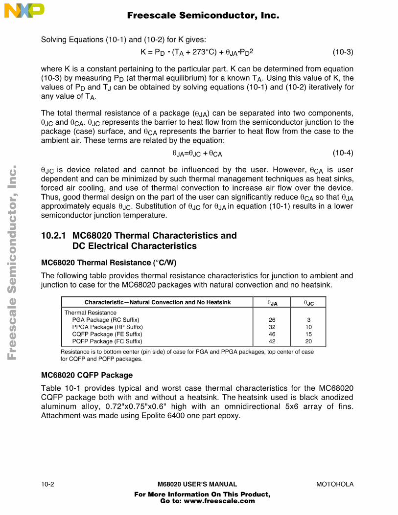
10-2 M68020 USERÕS MANUAL MOTOROLA
Solving Equations (10-1) and (10-2) for K gives:
K = PD ¥ (TA + 273°C) + qJA¥PD2 (10-3)
where K is a constant pertaining to the particular part. K can be determined from equation(10-3) by measuring PD (at thermal equilibrium) for a known TA. Using this value of K, thevalues of PD and TJ can be obtained by solving equations (10-1) and (10-2) iteratively forany value of TA.
The total thermal resistance of a package (qJA) can be separated into two components,qJC and qCA. qJC represents the barrier to heat flow from the semiconductor junction to thepackage (case) surface, and qCA represents the barrier to heat flow from the case to theambient air. These terms are related by the equation:
qJA=qJC + qCA (10-4)
qJC is device related and cannot be influenced by the user. However, qCA is userdependent and can be minimized by such thermal management techniques as heat sinks,forced air cooling, and use of thermal convection to increase air flow over the device.Thus, good thermal design on the part of the user can significantly reduce qCA so that qJAapproximately equals qJC. Substitution of qJC for qJA in equation (10-1) results in a lowersemiconductor junction temperature.
10.2.1 MC68020 Thermal Characteristics andDC Electrical Characteristics
MC68020 Thermal Resistance (°C/W)
The following table provides thermal resistance characteristics for junction to ambient andjunction to case for the MC68020 packages with natural convection and no heatsink.
CharacteristicÑNatural Convection and No Heatsink qJA qJC
Thermal ResistancePGA Package (RC Suffix)PPGA Package (RP Suffix)CQFP Package (FE Suffix)PQFP Package (FC Suffix)
26324642
3101520
Resistance is to bottom center (pin side) of case for PGA and PPGA packages, top center of casefor CQFP and PQFP packages.
MC68020 CQFP Package
Table 10-1 provides typical and worst case thermal characteristics for the MC68020CQFP package both with and without a heatsink. The heatsink used is black anodizedaluminum alloy, 0.72"x0.75"x0.6" high with an omnidirectional 5x6 array of fins.Attachment was made using Epolite 6400 one part epoxy.
Fre
esc
ale
Se
mic
on
du
cto
r, I
Freescale Semiconductor, Inc.
For More Information On This Product, Go to: www.freescale.com
nc
...

MOTOROLA M68020 USERÕS MANUAL 10-3
Table 10-1. qJA vs. AirflowÑMC68020 CQFP Package
Airflow in Linear Feet/Minute
qJA 0* 200 500
MaximumNo HeatsinkWith Heatsink
4635
2820
2418
TypicalNo HeatsinkWith Heatsink
4332
2517
2115
*Natural convection
Table 10-2 shows the relationship between clock speed and power dissipation for anypackage type. The worst case operating conditions are used for thermal managementdesign, while typical values are used for reliability analysis.
Table 10-2. Power vs. Rated Frequency(at TJ Maximum = 110°C)
Rated Frequency (MHz) PD Maximum (Watts) PD Typical (Watts)
33252016
1.41.21.00.9
0.840.720.600.54
Table 10-3 shows the relationship between board temperature rise and power dissipationin the test environment for the CQFP package. Derate qJA based on measurements madein the application by adding (0.8/PD) * [Tba(application) Ð Tba(table)] to the qJA values in thetable. Board temperature was measured on the top surface of the board directly under thedevice.
Table 10-3. Temperature Rise of Board vs. PDÑMC68020 CQFP Package
PD
Natural Convection 0.6W 1.0W 1.75W
Tba (°C)ÑNo Heatsink 18 27 53
Values for thermal resistance presented in this document were derived using theprocedure described in Motorola Reliability Report 7843, ÒThermal ResistanceMeasurement Method for MC68XX Microcomponent Devices,Ó and are provided fordesign purposes only. Thermal measurements are complex and dependent on procedureand setup. User-derived values for thermal resistance may differ.
Fre
esc
ale
Se
mic
on
du
cto
r, I
Freescale Semiconductor, Inc.
For More Information On This Product, Go to: www.freescale.com
nc
...
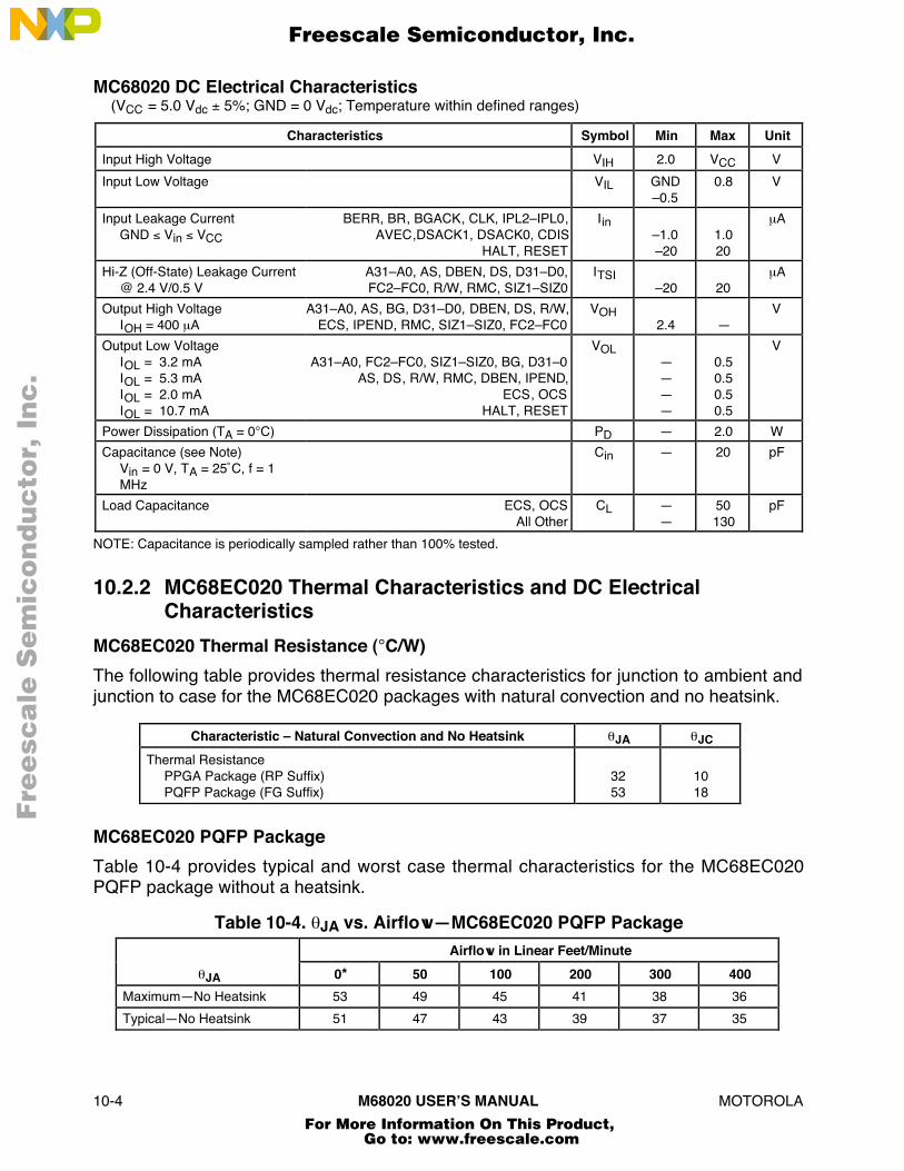
10-4 M68020 USERÕS MANUAL MOTOROLA
MC68020 DC Electrical Characteristics(VCC = 5.0 Vdc ± 5%; GND = 0 Vdc; Temperature within defined ranges)
Characteristics Symbol Min Max Unit
Input High Voltage VIH 2.0 VCC V
Input Low Voltage VIL GNDÐ0.5
0.8 V
Input Leakage CurrentGND £ Vin £ VCC
BERR, BR, BGACK, CLK, IPL2ÐIPL0,AVEC,DSACK1, DSACK0, CDIS
HALT, RESET
IinÐ1.0Ð20
1.020
mA
Hi-Z (Off-State) Leakage Current@ 2.4 V/0.5 V
A31ÐA0, AS, DBEN, DS, D31ÐD0,FC2ÐFC0, R/W, RMC, SIZ1ÐSIZ0
ITSIÐ20 20
mA
Output High VoltageIOH = 400 mA
A31ÐA0, AS, BG, D31ÐD0, DBEN, DS, R/W,ECS, IPEND, RMC, SIZ1ÐSIZ0, FC2ÐFC0
VOH2.4 Ñ
V
Output Low VoltageIOL = 3.2 mAIOL = 5.3 mAIOL = 2.0 mAIOL = 10.7 mA
A31ÐA0, FC2ÐFC0, SIZ1ÐSIZ0, BG, D31Ð0AS, DS, R/W, RMC, DBEN, IPEND,
ECS, OCSHALT, RESET
VOLÑÑÑÑ
0.50.50.50.5
V
Power Dissipation (TA = 0°C) PD Ñ 2.0 W
Capacitance (see Note)Vin = 0 V, TA = 25ûC, f = 1MHz
Cin Ñ 20 pF
Load Capacitance ECS, OCSAll Other
CL ÑÑ
50130
pF
NOTE: Capacitance is periodically sampled rather than 100% tested.
10.2.2 MC68EC020 Thermal Characteristics and DC ElectricalCharacteristics
MC68EC020 Thermal Resistance (°C/W)
The following table provides thermal resistance characteristics for junction to ambient andjunction to case for the MC68EC020 packages with natural convection and no heatsink.
Characteristic Ð Natural Convection and No Heatsink qJA qJC
Thermal ResistancePPGA Package (RP Suffix)PQFP Package (FG Suffix)
3253
1018
MC68EC020 PQFP Package
Table 10-4 provides typical and worst case thermal characteristics for the MC68EC020PQFP package without a heatsink.
Table 10-4. qJA vs. AirflowÑMC68EC020 PQFP Package
Airflow in Linear Feet/Minute
qJA 0* 50 100 200 300 400
MaximumÑNo Heatsink 53 49 45 41 38 36
TypicalÑNo Heatsink 51 47 43 39 37 35
Fre
esc
ale
Se
mic
on
du
cto
r, I
Freescale Semiconductor, Inc.
For More Information On This Product, Go to: www.freescale.com
nc
...
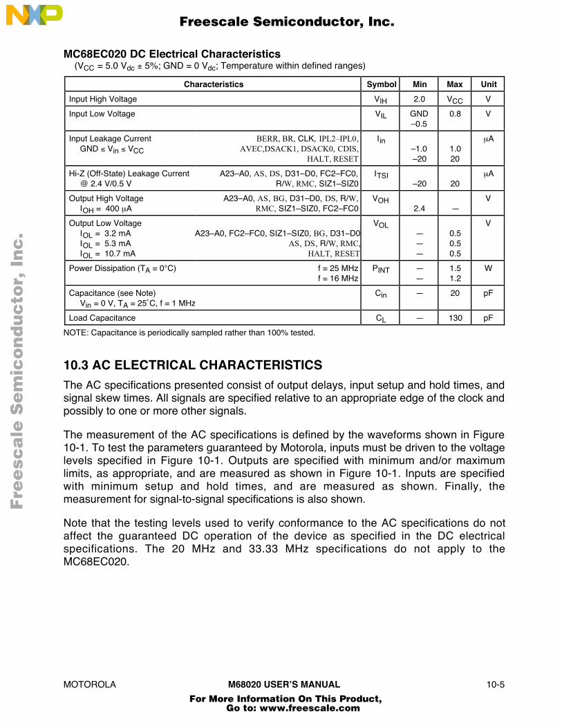
MOTOROLA M68020 USERÕS MANUAL 10-5
MC68EC020 DC Electrical Characteristics(VCC = 5.0 Vdc ± 5%; GND = 0 Vdc; Temperature within defined ranges)
Characteristics Symbol Min Max Unit
Input High Voltage VIH 2.0 VCC V
Input Low Voltage VIL GNDÐ0.5
0.8 V
Input Leakage CurrentGND £ Vin £ VCC
BERR, BR, CLK, IPL2ÐIPL0,AVEC,DSACK1, DSACK0, CDIS,
HALT, RESET
IinÐ1.0Ð20
1.020
mA
Hi-Z (Off-State) Leakage Current@ 2.4 V/0.5 V
A23ÐA0, AS, DS, D31ÐD0, FC2ÐFC0,R/W, RMC, SIZ1ÐSIZ0
ITSIÐ20 20
mA
Output High VoltageIOH = 400 mA
A23ÐA0, AS, BG, D31ÐD0, DS, R/W,RMC, SIZ1ÐSIZ0, FC2ÐFC0
VOH2.4 Ñ
V
Output Low VoltageIOL = 3.2 mAIOL = 5.3 mAIOL = 10.7 mA
A23ÐA0, FC2ÐFC0, SIZ1ÐSIZ0, BG, D31ÐD0AS, DS, R/W, RMC,
HALT, RESET
VOLÑÑÑ
0.50.50.5
V
Power Dissipation (TA = 0°C) f = 25 MHzf = 16 MHz
PINT ÑÑ
1.51.2
W
Capacitance (see Note)Vin = 0 V, TA = 25ûC, f = 1 MHz
Cin Ñ 20 pF
Load Capacitance CL Ñ 130 pF
NOTE: Capacitance is periodically sampled rather than 100% tested.
10.3 AC ELECTRICAL CHARACTERISTICS
The AC specifications presented consist of output delays, input setup and hold times, andsignal skew times. All signals are specified relative to an appropriate edge of the clock andpossibly to one or more other signals.
The measurement of the AC specifications is defined by the waveforms shown in Figure10-1. To test the parameters guaranteed by Motorola, inputs must be driven to the voltagelevels specified in Figure 10-1. Outputs are specified with minimum and/or maximumlimits, as appropriate, and are measured as shown in Figure 10-1. Inputs are specifiedwith minimum setup and hold times, and are measured as shown. Finally, themeasurement for signal-to-signal specifications is also shown.
Note that the testing levels used to verify conformance to the AC specifications do notaffect the guaranteed DC operation of the device as specified in the DC electricalspecifications. The 20 MHz and 33.33 MHz specifications do not apply to theMC68EC020.
Fre
esc
ale
Se
mic
on
du
cto
r, I
Freescale Semiconductor, Inc.
For More Information On This Product, Go to: www.freescale.com
nc
...

10-6 M68020 USERÕS MANUAL MOTOROLA
0.8 V
2.0 V
B
ADRIVE TO0.5 V
2.0 V
0.8 V
VALIDOUTPUT n
VALIDOUTPUT n + 1
2.0 V
0.8 V
2.0 V
0.8 V
2.0 V
0.8 V
VALIDOUTPUT n
VALIDOUTPUT n+1
2.0 V
0.8 V
B
A
VALIDINPUT
2.0 V
0.8 V
2.0 V
0.8 V
DC
DRIVE TO0.5 V
DRIVE TO2.4 V
VALIDINPUT
2.0 V
0.8 V
2.0 V
0.8 V
DC
DRIVETO 0.5 V
DRIVETO 2.4 V
2.0 V
0.8 V
2.0 V
0.8 V
F
E
CLK
OUTPUTS CLK
OUTPUTS CLK
INPUTS CLK
INPUTS CLK
ALL SIGNALS
NOTES:1. This output timing is applicable to all parameters specified relative to the rising edge of the clock.�2. This output timing is applicable to all parameters specified relative to the falling edge of the clock.�3. This input timing is applicable to all parameters specified relative to the rising edge of the clock.�4. This input timing is applicable to all parameters specified relative to the falling edge of the clock.�5. This timing is applicable to all parameters specified relative to the assertion/negation of another signal.
����
LEGEND:A. Maximum output delay specification.�B. Minimum output hold time.�C. Minimum input setup time specification.�D. Minimum input hold time specification.�E. Signal valid to signal valid specification (maximum or minimum).�F. Signal valid to signal invalid specification (maximum or minimum).
��
���
FIGURE 10-1MC68020UM
DRIVETO 2.4 V
1
2
3
4
5
Figure 10-1. Drive Levels and Test Points for AC Specifications
Fre
esc
ale
Se
mic
on
du
cto
r, I
Freescale Semiconductor, Inc.
For More Information On This Product, Go to: www.freescale.com
nc
...
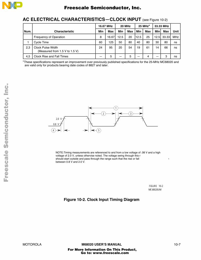
MOTOROLA M68020 USERÕS MANUAL 10-7
AC ELECTRICAL CHARACTERISTICSÑCLOCK INPUT (see Figure 10-2)
16.67 MHz 20 MHz 25 MHz* 33.33 MHz
Num. Characteristic Min Max Min Max Min Max Min Max Unit
Frequency of Operation 8 16.67 12.5 20 12.5 25 12.5 33.33 MHz
1 Cycle Time 60 125 50 80 40 80 30 80 ns
2,3 Clock Pulse Width(Measured from 1.5 V to 1.5 V)
24 95 20 54 19 61 14 66 ns
4,5 Clock Rise and Fall Times Ñ 5 Ñ 5 Ñ 4 Ñ 3 ns
*These specifications represent an improvement over previously published specifications for the 25-MHz MC68020 andare valid only for products bearing date codes of 8827 and later.
0.8 V
2.0 V
FIGURE 10-2MC68020UM
4 5
2
1
3
NOTE:���Timing measurements are referenced to and from a low voltage of .08 V and a high����������������voltage of 2.0 V, unless othervise noted. The voltage swing through this r a���������������should start outside and pass through the range such that the rise or fall w���������������between 0.8 V and 2.0 V.�������
Figure 10-2. Clock Input Timing Diagram
Fre
esc
ale
Se
mic
on
du
cto
r, I
Freescale Semiconductor, Inc.
For More Information On This Product, Go to: www.freescale.com
nc
...

10-8 M68020 USERÕS MANUAL MOTOROLA
AC ELECTRICAL CHARACTERISTICSÑREAD AND WRITE CYCLES(VCC = 5.0 Vdc ± 5%; GND = 0 Vdc; Temperature within defined ranges; see Figures 10-3Ð10-5)
16.67 MHz 20 MHz 25 MHz** 33.33 MHz
Num. Characteristics Min Max Min Max Min Max Min Max Unit
6 Clock High to FC, Size, RMC, Address Valid 0 30 0 25 0 25 0 21 ns
*6A Clock High to ECS, OCS Asserted 0 20 0 15 0 12 0 10 ns
7 Clock High to Address, Data, FC, Size, RMCHigh Impedance
0 60 0 50 0 40 0 30 ns
8 Clock High to Address, FC, Size,RMC Invalid
0 Ñ 0 Ñ 0 Ñ 0 Ñ ns
9 Clock Low to AS, DS Asserted 3 30 3 25 3 18 3 15 ns
9A1 AS to DS Assertion Skew (Read) Ð15 15 Ð10 10 Ð10 10 Ð10 10 ns
9B11 AS Asserted to DS Asserted (Write) 37 Ñ 32 Ñ 27 Ñ 22 Ñ ns
*10 ECS Width Asserted 20 Ñ 15 Ñ 15 Ñ 10 Ñ ns
*10A OCS Width Asserted 20 Ñ 15 Ñ 15 Ñ 10 Ñ ns
*10B7 ECS, OCS Width Negated 15 Ñ 10 Ñ 5 Ñ 5 Ñ ns
11 Address, FC, Size, RMC Valid to AS(and DS Asserted, Read)
15 Ñ 10 Ñ 6 Ñ 5 Ñ ns
12 Clock Low to AS, DS Negated 0 30 0 25 0 15 0 15 ns
*12A Clock Low to ECS, OCS Negated 0 30 0 25 0 15 0 15 ns
13 AS, DS Negated to Address, FC, Size,RMC Invalid
15 Ñ 10 Ñ 10 Ñ 5 Ñ ns
14 AS (and DS Read) Width Asserted 100 Ñ 85 Ñ 70 Ñ 50 Ñ ns
14A DS Width Asserted (Write) 40 Ñ 38 Ñ 30 Ñ 25 Ñ ns
15 AS, DS Width Negated 40 Ñ 38 Ñ 30 Ñ 23 Ñ ns
15A8 DS Negated to AS Asserted 35 Ñ 30 Ñ 25 Ñ 18 Ñ ns
16 Clock High to AS, DS, R/W, DBENHigh Impedance
Ñ 60 Ñ 50 Ñ 40 Ñ 30 ns
17 AS, DS Negated to R/W Invalid 15 Ñ 10 Ñ 10 Ñ 5 Ñ ns
18 Clock High to R/W High 0 30 0 25 0 20 0 15 ns
20 Clock High to R/W Low 0 30 0 25 0 20 0 15 ns
21 R/W High to AS Asserted (Read) 15 Ñ 10 Ñ 5 Ñ 5 Ñ ns
22 R/W Low to DS Asserted (Write) 75 Ñ 60 Ñ 50 Ñ 35 Ñ ns
23 Clock High to Data-Out Valid Ñ 30 Ñ 25 Ñ 25 Ñ 18 ns
25 AS, DS Negated to Data-Out Invalid 15 Ñ 10 Ñ 5 Ñ 5 Ñ ns
*25A9 DS Negated to DBEN Negated (Write) 15 Ñ 10 Ñ 5 Ñ 5 Ñ ns
26 Data-Out Valid to DS Asserted (Write) 15 Ñ 10 Ñ 5 Ñ 5 Ñ ns
27 Data-In Valid to Clock Low (Setup) (Read) 5 Ñ 5 Ñ 5 Ñ 5 Ñ ns
27A Late BERR/HALT Asserted to Clock Low(Setup)
20 Ñ 15 Ñ 10 Ñ 5 Ñ ns
28 AS, DS Negated to DSACK», BERR, HALT,AVEC Negated
0 80 0 65 0 50 0 40 ns
Fre
esc
ale
Se
mic
on
du
cto
r, I
Freescale Semiconductor, Inc.
For More Information On This Product, Go to: www.freescale.com
nc
...

MOTOROLA M68020 USERÕS MANUAL 10-9
AC ELECTRICAL CHARACTERISTICSÑREAD AND WRITE CYCLES(Continued)
16.67 MHz 20 MHz 25 MHz** 33.33 MHz
Num. Characteristics Min Max Min Max Min Max Min Max Unit
29 AS, DS Negated to Data-In Invalid(Data-In Hold Time)
0 Ñ 0 Ñ 0 Ñ 0 Ñ ns
29A AS, DS Negated to Data-In(High Impedance)
Ñ 60 Ñ 50 Ñ 40 Ñ 30 ns
30 Clock Low to Data-In Invalid(Data-In Hold Time)
15 Ñ 15 Ñ 10 Ñ 10 Ñ ns
312 DSACK» Asserted to Data-In Valid Ñ 50 Ñ 43 Ñ 32 Ñ 17 ns
31A3 DSACK» Asserted to DSACK» Valid(DSACK» Asserted Skew)
Ñ 15 Ñ 10 Ñ 10 Ñ 10 ns
32 RESET Input Transition Time Ñ 1.5 Ñ 1.5 Ñ 1.5 Ñ 1.5 Clks
33 Clock Low to BG Asserted 0 30 0 25 0 20 0 20 ns
34 Clock Low to BG Negated 0 30 0 25 0 20 0 20 ns
35 BR Asserted to BG Asserted (RMC NotAsserted)
1.5 3.5 1.5 3.5 1.5 3.5 1.5 3.5 Clks
*37 BGACK Asserted to BG Negated 1.5 3.5 1.5 3.5 1.5 3.5 1.5 3.5 Clks
*37A6 BGACK Asserted to BR Negated 0 1.5 0 1.5 0 1.5 0 1.5 Clks
39 BG Width Negated 90 Ñ 75 Ñ 60 Ñ 50 Ñ ns
39A BG Width Asserted 90 Ñ 75 Ñ 60 Ñ 50 Ñ ns
*40 Clock High to DBEN Asserted (Read) 0 30 0 25 0 20 0 15 ns
*41 Clock Low to DBEN Negated (Read) 0 30 0 25 0 20 0 15 ns
*42 Clock Low to DBEN Asserted (Write) 0 30 0 25 0 20 0 15 ns
*43 Clock High to DBEN Negated (Write) 0 30 0 25 0 20 0 15 ns
*44 R/W Low to DBEN Asserted (Write) 15 Ñ 10 Ñ 10 Ñ 5 Ñ ns
*455 DBEN Width Asserted ReadWrite
60120
ÑÑ
50100
ÑÑ
4080
ÑÑ
3060
ÑÑ
ns
46 R/W Width Valid (Write or Read) 150 Ñ 125 Ñ 100 Ñ 75 Ñ ns
47A Asynchronous Input Setup Time 5 Ñ 5 Ñ 5 Ñ 5 Ñ ns
47B Asynchronous Input Hold Time 15 Ñ 15 Ñ 10 Ñ 10 Ñ ns
484 DSACK» Asserted to BERR, HALT Asserted Ñ 30 Ñ 20 Ñ 18 Ñ 15 ns
53 Data-Out Hold from Clock High 0 Ñ 0 Ñ 0 Ñ 0 Ñ ns
55 R/W Valid to Data Bus Impedance Change 30 Ñ 25 Ñ 20 Ñ 20 Ñ ns
56 RESET Pulse Width (Reset Instruction) 512 Ñ 512 Ñ 512 Ñ 512 Ñ Clks
57 BERR Negated to HALT Negated (Rerun) 0 Ñ 0 Ñ 0 Ñ 0 Ñ ns
*5810 BGACK Negated to Bus Driven 1 Ñ 1 Ñ 1 Ñ 1 Ñ Clks
5910 BG Negated to Bus Driven 1 Ñ 1 Ñ 1 Ñ 1 Ñ Clks
*This specification does not apply to the MC68EC020.**These specifications represent an improvement over previously published specifications for the 25-MHz MC68020
and are valid only for product bearing date codes of 8827 and later.
Fre
esc
ale
Se
mic
on
du
cto
r, I
Freescale Semiconductor, Inc.
For More Information On This Product, Go to: www.freescale.com
nc
...

10-10 M68020 USERÕS MANUAL MOTOROLA
AC ELECTRICAL CHARACTERISTICSÑREAD AND WRITE CYCLES(Concluded)
NOTES:1. This number can be reduced to 5 ns if strobes have equal loads.2. If the asynchronous setup time (#47A) requirements are satisfied, the DSACK» low to data setup time (#31) and
DSACK» low to BERR low setup time (#48) can be ignored. The data must only satisfy the data-in clock lowsetup time (#27) for the following clock cycle, and BERR must only satisfy the late BERR low to clock low setuptime (#27A) for the following clock cycle.
3. This parameter specifies the maximum allowable skew between DSACK0 to DSACK1 asserted or DSACK1 toDSACK0 asserted; specification #47A must be met by DSACK0 or DSACK1.
4. This specification applies to the first (DSACK0 or DSACK1) DSACK» signal asserted. In the absence ofDSACK», BERR is an asynchronous input using the asynchronous input setup time (#47A).
5. DBEN may stay asserted on consecutive write cycles.6. The minimum values must be met to guarantee proper operation. If this maximum value is exceeded, BG may
be reasserted.7. This specification indicates the minimum high time for ECS and OCS in the event of an internal cache hit
followed immediately by a cache miss or operand cycle.8. This specification guarantees operation with the MC68881/MC68882, which specifies a minimum time for DS
negated to AS asserted (specification #13A in MC68881UM/AD, MC68881/MC68882 Floating-PointCoprocessor User's Manual). Without this specification, incorrect interpretation of specifications #9A and #15would indicate that the MC68020/EC020 does not meet the MC68881/MC68882 requirements.
9. This specification allows a system designer to guarantee data hold times on the output side of data buffers thathave output enable signals generated with DBEN.
10. These specifications allow system designers to guarantee that an alternate bus master has stopped driving thebus when the MC68020/EC020 regains control of the bus after an arbitration sequence.
11. This specification allows system designers to qualify the CS signal of an MC68881/MC68882 with AS (allowing7 ns for a gate delay) and still meet the CS to DS setup time requirement (specification 8B of MC68881UM/AD,MC68881/MC68882 Floating-Point Coprocessor User's Manual).
Fre
esc
ale
Se
mic
on
du
cto
r, I
Freescale Semiconductor, Inc.
For More Information On This Product, Go to: www.freescale.com
nc
...

MOTOROLA M68020 USERÕS MANUAL 10-11
R/W
FIGURE 10-3MC68020UM
S0 S1 S2 S3 S4 S5
*A31–A0
CLK
7
FC2–FC0
SIZ1–SIZ0
**ECS
OCS
DS
AS
**DBEN
BERR
HALT
DSACK0
DSACK1
D31–D0
29A
2927
40
47A47B
48
45
31
28
21
189
31A
17
12
14
11
16
10
10A
6A
8
6
ALLASYNCHRONOUS
INPUTS
12A
13
Timing measurements are referenced to and from a low voltage of 0.8 V�and a high voltage of 2.0 V, unless otherwise noted. The voltage swing�through this range should start outside and pass through the range such�that the rise or fall will be linear between 0.8 V and 2.0 V.
���
NOTE:
�*For the MC68EC020, A23ÐA0.�**This signal does not apply to the MC68EC020.� �
27A
41
30
46
�
Figure 10-3. Read Cycle Timing Diagram
Fre
esc
ale
Se
mic
on
du
cto
r, I
Freescale Semiconductor, Inc.
For More Information On This Product, Go to: www.freescale.com
nc
...
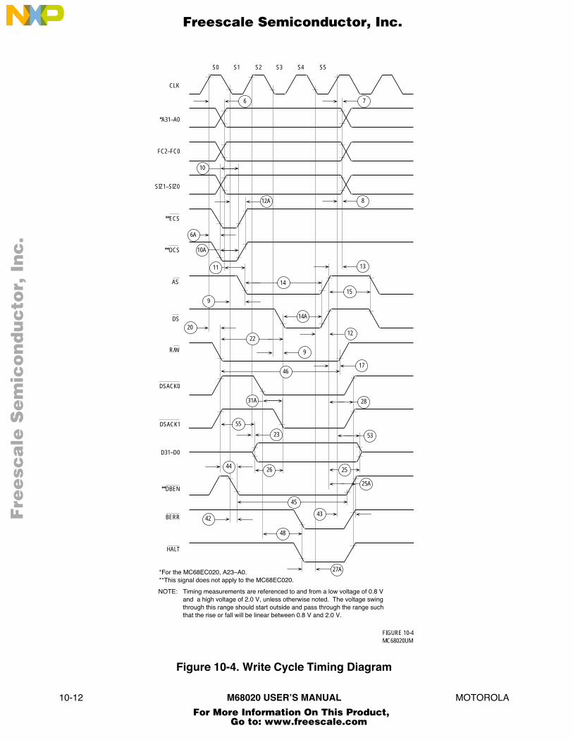
10-12 M68020 USERÕS MANUAL MOTOROLA
D31–D0
R/W
FIGURE 10-4MC68020UM
S0 S1 S2 S3 S4 S5
*A31–A0
CLK
7
FC2–FC0
SIZ1–SIZ0
**ECS
**OCS
DS
AS
**DBEN
BERR
HALT
DSACK0
DSACK1
53
27A
48
45
23
28
20
9
31A
12
14
11
10
10A
6A
8
6
12A
13
15
14A
22
17
55
42
4425
46
9
Timing measurements are referenced to and from a low voltage of 0.8 V�and a high voltage of 2.0 V, unless otherwise noted. The voltage swing�through this range should start outside and pass through the range such�that the rise or fall will be linear between 0.8 V and 2.0 V.
���
NOTE:
26
� *For the MC68EC020, A23ÐA0.�**This signal does not apply to the MC68EC020.�
�
43
25A
Figure 10-4. Write Cycle Timing Diagram
Fre
esc
ale
Se
mic
on
du
cto
r, I
Freescale Semiconductor, Inc.
For More Information On This Product, Go to: www.freescale.com
nc
...

MOTOROLA M68020 USERÕS MANUAL 10-13
FIGURE 10-5MC68020UM
S0 S1 S2 S3 S4 S5
*A31–A0
CLK
7
FC2–FC0
SIZ1–SIZ0
**ECS
OCS
DS
R/W
AS
DBEN
BR
DSACK0
DSACK1
D31–D0
33
BG
**BGACK
16
35
37
39A
34
39
Timing measurements are referenced to and from a low voltage of 0.8 V and a high voltage�of 2.0 V, unless otherwise noted. The voltage swing through this range should start outside�and pass through the range such that the rise or fall will be linear between 0.8 V and 2.0 V.
��
NOTE:
*For the MC68EC020, A23ÐA0.�**This signal does not apply to the MC68EC020.�
37A
59
58
�
Figure 10-5. Bus Arbitration Timing Diagram
Fre
esc
ale
Se
mic
on
du
cto
r, I
Freescale Semiconductor, Inc.
For More Information On This Product, Go to: www.freescale.com
nc
...

10-14 M68020 USERÕS MANUAL MOTOROLA
Fre
esc
ale
Se
mic
on
du
cto
r, I
Freescale Semiconductor, Inc.
For More Information On This Product, Go to: www.freescale.com
nc
...

MOTOROLA MC68838 USER’S MANUAL 13-1
SECTION 11ORDERING INFORMATION AND MECHANICAL DATA
This section contains the pin assignments and package dimensions of the MC68020 andthe MC68EC020. In addition, detailed information is provided to be used as a guide whenordering.
11.1 STANDARD ORDERING INFORMATION
11.1.1 Standard MC68020 Ordering Information
Package Type Frequency (MHz) Temperature (°C) Order Number
Ceramic Pin Grid ArrayRC Suffix 16.67
20.025.0
33.33
0 to 700 to 700 to 700 to 70
MC68020RC16MC68020RC20MC68020RC25MC68020RC33
Plastic Quad Flat PackFC Suffix 16.67
20.025.0
0 to 700 to 700 to 70
MC68020FC16MC68020FC20MC68020FC25
Plastic Pin Grid ArrayRP Suffix 16.67
20.025.0
0 to 700 to 700 to 70
MC68020RP16MC68020RP20MC68020RP25
Ceramic Quad Flat PackFE Suffix 16.67
20.025.0
33.33
0 to 700 to 700 to 700 to 70
MC68020FE16MC68020FE20MC68020FE25MC68020FE33
11.1.2 Standard MC68EC020 Ordering Information
Package Type Frequency (MHz) Temperature (°C) Order Number
Plastic Pin Grid ArrayRP Suffix 16.67
25.00 to 700 to 70
MC68EC020RP16MC68EC020RP25
Plastic Quad Flat PackFG Suffix 16.67
25.00 to 700 to 70
MC68EC020FG16MC68EC020FG25
Fre
esc
ale
Se
mic
on
du
cto
r, I
Freescale Semiconductor, Inc.
For More Information On This Product, Go to: www.freescale.com
nc
...
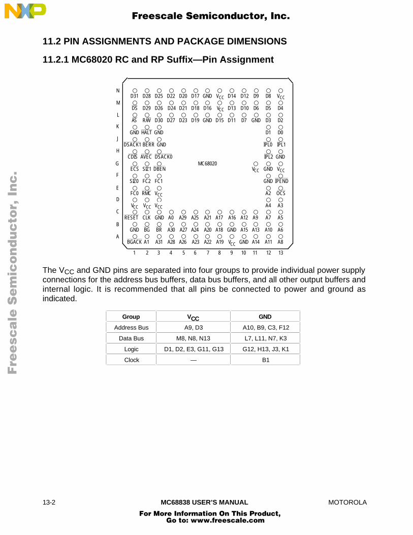
13-2 MC68838 USER’S MANUAL MOTOROLA
11.2 PIN ASSIGNMENTS AND PACKAGE DIMENSIONS
11.2.1 MC68020 RC and RP Suffix—Pin Assignment
GND
ECS
SIZ0
FC0
RESET
GND
BGACK
HALT
FC2
RMC
A1
GND
GND
BR
A31
A30
A28
A27
A26
A24
A23
A20
A22
A18
A19
A17 A16
GND
A12
A15
GND
DSACK1 BERR
AVEC DSACK0
SIZ1
1 2 3 4 5 6 7 8 9 10
A
B
C
D
E
F
G
H
J
K
BG
L
M
N
11 12 13
D1 D0
AS R/W D30 D27 D23 D19 GND D15 D11 D7 GND D3 D2
DS D29 D26 D24 D21 D18 D16 D13 D10 D6 D5 D4
D31 D28 D25 D22 D20 D17 GND D14 D12 D9 D8
IPL0 IPL1
IPL2 GND
GND
GND IPEND
A2 OCS
A4 A3
A9 A7 A5
A13 A10 A6
A14 A11 A8
A21A25A29A0
CDIS
DBEN
FC1
V V
V
V V
V
V V
V
CLK GND
V
CC CC
CC
CC
CC
CC CC
CC
CC
CC
MC68020
The VCC and GND pins are separated into four groups to provide individual power supplyconnections for the address bus buffers, data bus buffers, and all other output buffers andinternal logic. It is recommended that all pins be connected to power and ground asindicated.
Group VCC GND
Address Bus A9, D3 A10, B9, C3, F12
Data Bus M8, N8, N13 L7, L11, N7, K3
Logic D1, D2, E3, G11, G13 G12, H13, J3, K1
Clock — B1
Fre
esc
ale
Se
mic
on
du
cto
r, I
Freescale Semiconductor, Inc.
For More Information On This Product, Go to: www.freescale.com
nc
...

MOTOROLA MC68838 USER’S MANUAL 13-3
11.2.2 MC68020 RC Suffix—Package Dimensions
C
K
1 2 3 4 5 6 7 8 9 10 11 12 13
ABCDEFGH
KLMN
J
G
G
RC SUFFIXCASE 791-01MC68020 T
NOTES: 1. A AND B ARE DATUMS AND T IS A DATUM SURFACE. 2. POSITIONAL TOLERANCE FOR LEADS (114 PLACES).
3. DIMENSIONING AND TOLERANCING PER Y14.5M,1982. 4. CONTROLLING DIMENSION: INCH.
D
0.13 (0.005) M T A S B S
DIM
MILLIMETERS INCHES
MIN MAX MIN MAX
A
B
C
D
G
1.340 1.380
1.340 1.380
0.100 0.150
34.04 35.05
34.04 35.05
2.54 3.81
0.43 0.55 0.017 0.022
0.100 BSC2.54 BSC
K 4.32 4.95 0.170 0.195
φB
A
Fre
esc
ale
Se
mic
on
du
cto
r, I
Freescale Semiconductor, Inc.
For More Information On This Product, Go to: www.freescale.com
nc
...

13-4 MC68838 USER’S MANUAL MOTOROLA
11.2.3 MC68020 RP Suffix—Package Dimensions
C
K
1 2 3 4 5 6 7 8 9 10 11 12 13
ABCDEFGH
KLMN
J
G
G
RP SUFFIXCASE 789E-02MC68020
A
B
T
NOTES: 1. DIMENSIONING AND TOLERANCING PER ANSI Y14.5M, 1982. 2. CONTROLLING DIMENSION: INCH. 3. DIMENSION D INCLUDES LEAD FINISH. 4. 789E-01 OBSOLETE. NEW STANDARD 789E-02.
D 114 PL
DIM
MILLIMETERS INCHES
MIN MAX MIN MAX
A
B
C
D
G
1.340 1.380
1.340 1.380
0.115 0.135
34.04 35.05
34.04 35.05
2.92 3.18
0.44 0.55 0.017 0.022
0.100 BSC2.54 BSC
K 2.79 3.81 0.110 0.150
V
V
0.76 (0.030) M T A S B Sφ
T
0.25 (0.010)φ X
0.17 (0.007)
M
M
X
L
L
V
1.02 1.52 0.040 0.060
30.48 BSC 1.200 BSC
PINA-1
Fre
esc
ale
Se
mic
on
du
cto
r, I
Freescale Semiconductor, Inc.
For More Information On This Product, Go to: www.freescale.com
nc
...
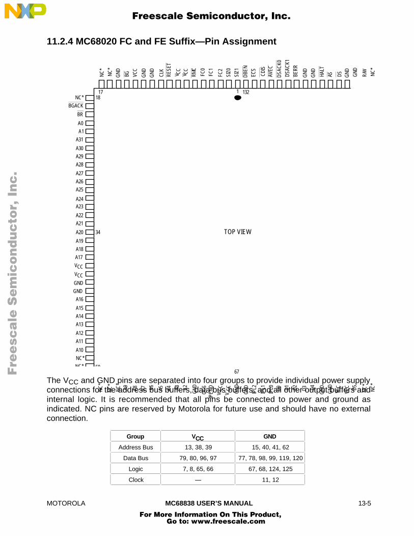
MOTOROLA MC68838 USER’S MANUAL 13-5
11.2.4 MC68020 FC and FE Suffix—Pin Assignment
18
50
17 1
34
VCC
67
132
NC
*
NC
*
NC
*A9 A8 A7 A6 A5 A4 A3 A2
GND
GND
GND D0 D1 D2 D3 D4
GND GND D5 NC
*
NC
*
VCC
VCC V C
C
VCC
NC
*
NC
*
GND BG GND
GND CL
KRE
SET
V CC
V CC
RMC
FC0
FC1
FC2
SIZ0
SIZ1
DBE
N
ECS
CDIS
AVEC
DSA
CK0
DSA
CK1
BER
R
GND
GND HA
LT
AS R/W
NC
*
DS
GND GND
IPEN
DO
CS
IPL2
IPL1
IPL0
NC*
BGACK
BR
A0
A1
A31
A30
A29
A28
A27
A26
A25
A24A23
A22
A21
A20
A19
A18
A17
V
V
GND
GND
A16
A15
A14
A13
A12
A11
A10
NC*
NC*
CC
CC
TOP VIEW
The VCC and GND pins are separated into four groups to provide individual power supplyconnections for the address bus buffers, data bus buffers, and all other output buffers andinternal logic. It is recommended that all pins be connected to power and ground asindicated. NC pins are reserved by Motorola for future use and should have no externalconnection.
Group VCC GND
Address Bus 13, 38, 39 15, 40, 41, 62
Data Bus 79, 80, 96, 97 77, 78, 98, 99, 119, 120
Logic 7, 8, 65, 66 67, 68, 124, 125
Clock — 11, 12
Fre
esc
ale
Se
mic
on
du
cto
r, I
Freescale Semiconductor, Inc.
For More Information On This Product, Go to: www.freescale.com
nc
...

13-6 MC68838 USER’S MANUAL MOTOROLA
11.2.5 MC68020 FC Suffix—Package Dimensions
Z PIN 1 INDE
X
0.25 (0.010) T X Y ZS
D 132 PL
DIMA
MILLIMETERS INCHESMIN MAX MIN MAX
24.06 24.20 0.947 0.95324.06 24.20 0.947 0.9534.07 4.57 0.160 0.1800.21 0.30 0.008 0.012
0.64 BSC 0.025 BSC0.51 1.01 0.020 0.0400.16 0.20 0.006 0.008
0.030
NOTES: 1. DIMENSIONING AND TOLERANCING PER ANSI Y14.5M, 1982. 2. CONTROLLING DIMENSION: INCH 3. DIMENSIONS A, B, N, AND R DO NOT INCLUDE MOLD PROTRUSION ALLOWABLE MOLD PROTRUSION FOR DIMENSIONS A AND B IS 0.25 (0.010), FOR DIMENSIONS N AND R IS 0.18 (0.007). 4. DATUM PLANE -W- IS LOCATED AT THE UNDERSIDE OF LEADS WHERE LEADS EXIT PACKAGE BODY. 5. DATUMS -X-, -Y-, AND -Z- TO BE DETERMINED WHERE CENTER LEAPACKAGE BODY AT DATUM -W-.
Y
G
P P
S S S
0.05. (0.002)
0.20 (0.008) T X Y ZS S S S
0.20 (0.008) T X Y ZS S S S
0.25 (0.010) T X Y ZS S S S
0.05 (0.002)
N
S
A
H
C
0.20 (0.008) T X Y ZS S S S K
JSEATING PLANE
.10 (0.004)
T
SECTION P-P
BCDGHJK
FC SUFFIXCASE 831A-01MC68020
VLBR
Fre
esc
ale
Se
mic
on
du
cto
r, I
Freescale Semiconductor, Inc.
For More Information On This Product, Go to: www.freescale.com
nc
...

MOTOROLA MC68838 USER’S MANUAL 13-7
11.2.6 MC68020 FE Suffix—Package Dimensions
FE SUFFIXCASE 831-01MC68020
DIMABCDGHJKLMR
MILLIMETERS INCHESMIN MAX MIN MAX
21.85 22.86 0.860 0.90021.85 22.86 0.860 0.9003.94 4.31 0.155 0.170
0.204 0.292 0.0080 0.01150.64 BSC 0.025 BSC
0.64 0.88 0.025 0.0350.13 0.20 0.005 0.0080.51 0.76 0.020 0.030
0° 8 0 820.32 REF 0.800 REF
° ° °0.64 0.025
NOTES: 1. DIMENSIONING AND TOLERANCING PER ANSI Y14.5M, 1982. 2. CONTROLLING DIMENSION: INCH 3. DIMENSIONS A AND B DEFINE MAXIMUM CERAMIC BODY DIMENSIONS INCLUDING GLASS PROTRUSION AND MISMATCH OF CERAMIC BODYTOP AND BOTTOM. 4. DATUM PLANE -W- IS LOCATED AT THE UNDERSIDE OF LEADS WHERE LEADS EXIT PACKAGE BODY. 5. DATUMS -X-, -Y-, AND -Z- TO BE DETERMINED WHERE CENTER LEADS EXIT PACKAGE BODY AT DATUM -W-. 6. DIMENSIONS S AND V TO BE DETERMINED AT SEATING PLANE, DATUM -T-. 7. DIMENSIONS A AND B TO BE DETERMINED AT DATUM PLANE -W-.
W
0.10∩SEATING PLANE
D 132 PL
J
K
H
C
PIN 1 INDENT
X
0.51 (0.020) T X — Y
0.20 (0.008) T X — Y ZM S S S
S S Z SM
0.51 (0.020) T X — YS S Z SM
0.20 (0.008) T X — Y ZM S S S
R
0.20 (0.008) T X — Y ZM S S S
(0.004)T M
V B L
S
A
— —
Fre
esc
ale
Se
mic
on
du
cto
r, I
Freescale Semiconductor, Inc.
For More Information On This Product, Go to: www.freescale.com
nc
...
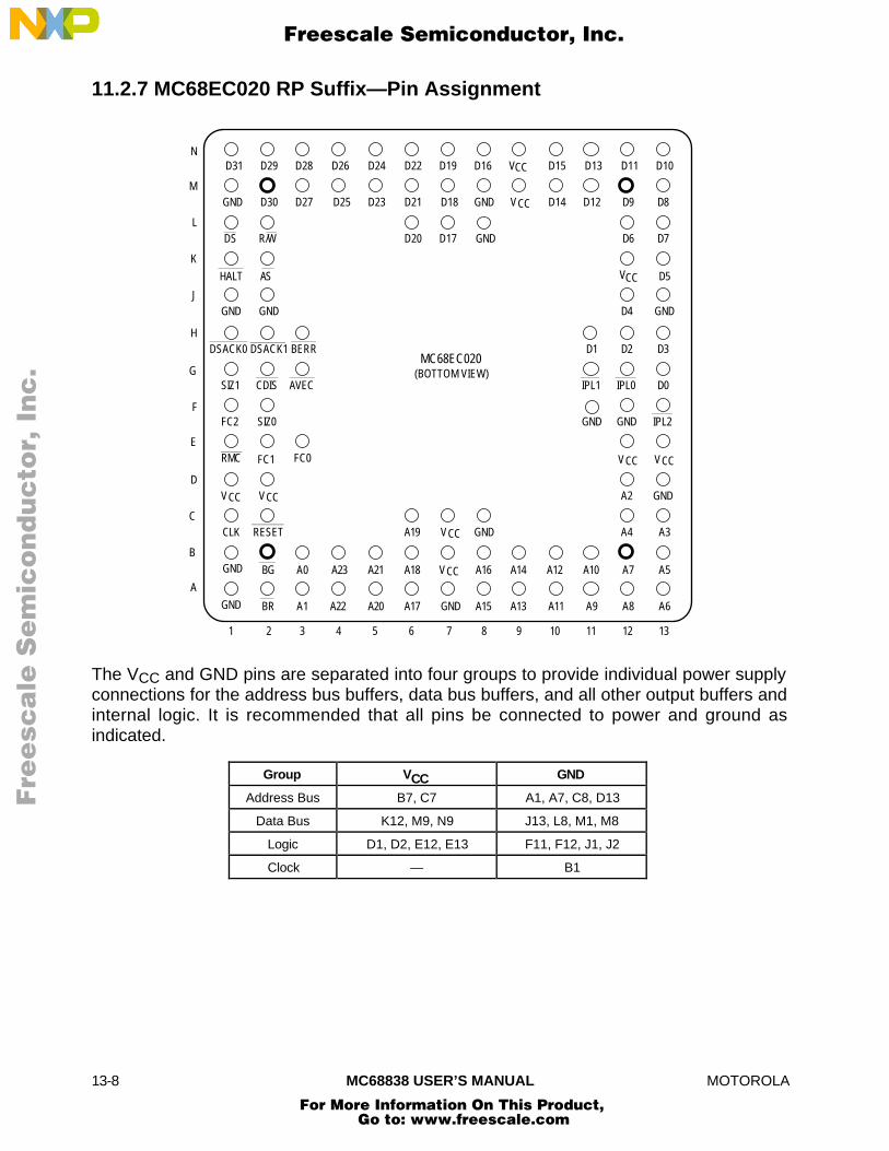
13-8 MC68838 USER’S MANUAL MOTOROLA
11.2.7 MC68EC020 RP Suffix—Pin Assignment
FC0RMC
SIZ0
AVEC
RESETCLK GND
A16
A15
A18
A17A20A22
A21A23A0BG
BR A1
1 2 3 4 5 6 7 8
(BOTTOM VIEW)
N
M
L
K
J
H
G
F
E
D
C
B
A
D31 D29 D28 D26 D24 D22 D19
D30 D27 D23 D21 D18
DS R/W D17
AS
DSACK1 BERR D2 D3
IPL0 D0
GND
IPL2
A3
A5
A6
A7
A8A9
A10A12
A11
11 12 13
D16 D15 D13 D11
GND D14 D12 D9 D8
D6 D7
9 10
A14
A4
SIZ1
GND
D5
D4
A2
MC68EC020
VCC
VCCD25
D20
HALT
DSACK0
FC2
A19
D10
GND
CDIS
FC1
GND
GND
IPL1
D1
VCC
GND GND
GND GND
VCC VCC
GND
GND
VCC
VCC VCC
VCC
A13
The VCC and GND pins are separated into four groups to provide individual power supplyconnections for the address bus buffers, data bus buffers, and all other output buffers andinternal logic. It is recommended that all pins be connected to power and ground asindicated.
Group VCC GND
Address Bus B7, C7 A1, A7, C8, D13
Data Bus K12, M9, N9 J13, L8, M1, M8
Logic D1, D2, E12, E13 F11, F12, J1, J2
Clock — B1
Fre
esc
ale
Se
mic
on
du
cto
r, I
Freescale Semiconductor, Inc.
For More Information On This Product, Go to: www.freescale.com
nc
...

MOTOROLA MC68838 USER’S MANUAL 13-9
11.2.8 MC68EC020 RP Suffix—Package Dimensions
C
S
1 2 3 4 5 6 7 8 9 10 11 12 13
ABCDEFGH
KLMN
J
G
G
RP SUFFIXCASE 789H-01MC68EC020
A
B
T
NOTES: 1. DIMENSIONING AND TOLERANCING PER ANSI Y14.5M, 1982. 2. CONTROLLING DIMENSION: INCH 3. DIMENSION D INCLUDES LEAD FINISH.
D 100 PL
DIM
MILLIMETERS INCHES
MIN MAX MIN MAX
A
B
C
D
G
1.340 1.380
1.340 1.380
0.115 0.135
34.04 35.05
34.04 35.05
2.92 3.18
0.44 0.55 0.017 0.022
0.100 BSC2.54 BSC
K 3.05 3.55 0.120 0.140
V
V
0.76 (0.030) M T A S B Sφ
T
0.25 (0.010)φ X
0.17 (0.007)
M
M
X
L
L 1.02 1.52 0.040 0.060
SV
4.32 4.83 0.170 0.19030.48 BSC 1.200 BSC
KPINA-1
Fre
esc
ale
Se
mic
on
du
cto
r, I
Freescale Semiconductor, Inc.
For More Information On This Product, Go to: www.freescale.com
nc
...

13-10 MC68838 USER’S MANUAL MOTOROLA
11.2.9 MC68EC020 FG Suffix—Pin Assignment
A9
1 3031
505180
81
100
A10
A11
A12
A13
A14
A15
A16
GND
A17
A18
A19
A20
A21
A22
A23
A1
A0
BR
VCC
BGA8
*
CLK
RESE
T
GND
GND
RMC
FC0
FC1
FC2
SIZ0
SIZ1
CDIS
AVEC
DSA
CK0
DSA
CK1
BERR
D7 D8
HALT AS DS
R/W D31
D30
D29
D28
D9
V CC
D27
D26
D25
D24
D23
D22
D21
D20
D19
D18
D17
D16
GND
D14
D13
D12
D11
D10
VCC
D15
GND V CC
D6D5GND
D4D3D2D1D0IPL0
IPL1
IPL2
GND
GND
GNDA2A3A4A5A6A7 V CC
V CC
MC68EC020(TOP VIEW)
NC*
NC
V CC
GND
GND
GND
GND
*NC—Do not connect to this pin.
The VCC and GND pins are separated into four groups to provide individual power supplyconnections for the address bus buffers, data bus buffers, and all other output buffers andinternal logic. It is recommended that all pins be connected to power and ground asindicated. NC pins are reserved by Motorola for future use and should have no externalconnection.
Group VCC GND
Address Bus 90 72, 89, 100
Data Bus 44, 57 26, 43, 58, 59
Logic 7, 8, 70, 71 3, 20, 21, 68, 69
Clock — 4
Fre
esc
ale
Se
mic
on
du
cto
r, I
Freescale Semiconductor, Inc.
For More Information On This Product, Go to: www.freescale.com
nc
...

MOTOROLA MC68838 USER’S MANUAL 13-11
11.2.10 MC68EC020 FG Suffix—Package Dimensions
0.25
A B
AA
0.20 (0.008) C A – B DM S S
0.50 (0.002)
D1 30
A
Z
50
31
51
B
80
Y
0.20
(0.0
08)
HA
– B
DM
SS
0.20
(0.0
08)
CA
– B
DM
SS
0.05
(0.0
02)
D
A – B
0.20 (0.008) H A – B DM S S
S
DETAIL "C"
UR
T
Q
KX
DIMA
MILLIMETERS INCHESMIN MAX MIN MAX
19.90 20.10 0.783 0.791
NOTES: 1. DIMENSIONING AND TOLERANCING PER ANSI Y14.5M, 1982. 2. CONTROLLING DIMENSION: MILLIMETER.3. DATUM PLANE -H- IS LOCATED AT BOTTOM OF LEAD AND ISCOINCIDENT WITH THE LEAD WHERE THE LEAD EXITS THEPLASTIC BODY AT THE BOTTOM OF THE PARTING LINE. 4. DATUMS -A-, -B-, AND -D- TO BE DETERMINED AT DATUM PLANE -H-.5. DIMENSIONS S AND V TO BE DETERMINED AT SEATING PLANE -C-.6. DIMENSIONS A AND B DO NOT INCLUDE MOLD PROTRUSION. ALLOWAPROTRUSION IS 0.25 (0.010) PER SIDE. DIMENSIONS A AND B DO INCLUDMOLD MISMATCH AND ARE DETERMINED AT DATUM PLANE -H-.7. DIMENSION D DOES NOT INCLUDE DAMBAR PROTRUSION. ALLOWABLDAMBAR PROTRUSION SHALL BE 0.08 (0.003) TOTAL IN EXCESS OF THE DDIMENSION AT MAXIMUM MATERIAL CONDITION. DAMBAR CANNOT BELOCATED ON THE LOWER RADIUS OR THE FOOT.
FG SUFFIXCASE 842D-01MC68EC020
C M
MH G
E
CSEATINGPLANE
H∩ 0.10 (0
DATUMPLANE
DETAIL "C
DETAIL "B"
F
N
BASE METALD
J
0.20 (0.008) C A – BM
DETAIL "A"
LV
DETAIL "A"
P
A, B, D
HDATUMPLANE
B 13.90 14.10 0.547 0.555C 3.30 0.130D 0.22 0.38 0.009 0.015E 2.55 3.05 0.100 0.120F 0.22 0.33 0.009 0.013G 0.65 BSC 0.026 BSCH 0.10 0.36 0.004 0.014J 0.13 0.23 0.005 0.009K 0.65 0.95 0.026 0.037L 12.35 REF 0.486 REFM 5 16 5 16N 0.13 0.17 0.005 0.007P 0.325 BSC 0.013 BSCQ 0 7 0 7R 0.35 0.010 0.014S 23.65 24.15 0.931 0.951T 0.13 0.005U 0 0V 17.65 18.15 0.695 0.715
° °
° ° ° °
° °
° °
81
100
— —
— —— —
Fre
esc
ale
Se
mic
on
du
cto
r, I
Freescale Semiconductor, Inc.
For More Information On This Product, Go to: www.freescale.com
nc
...
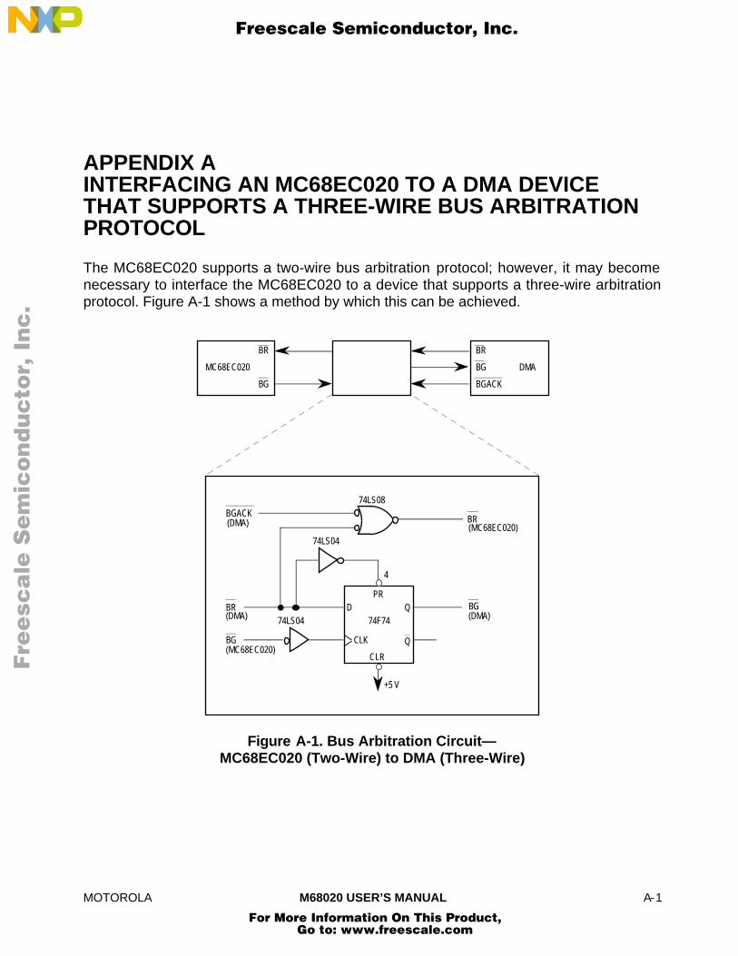
MOTOROLA M68020 USER’S MANUAL A-1
APPENDIX AINTERFACING AN MC68EC020 TO A DMA DEVICETHAT SUPPORTS A THREE-WIRE BUS ARBITRATIONPROTOCOL
The MC68EC020 supports a two-wire bus arbitration protocol; however, it may becomenecessary to interface the MC68EC020 to a device that supports a three-wire arbitrationprotocol. Figure A-1 shows a method by which this can be achieved.
BGPR
Q
Q
CLR
CLK
D
+5 V
74F74
4
74LS08
BRBGACK
BR
74LS04
74LS04
BG(MC68EC020)
(DMA)
(DMA)
(DMA)
(MC68EC020)
MC68EC020
BG
BR
BGACK
BR
BG DMA
Figure A-1. Bus Arbitration Circuit—MC68EC020 (Two-Wire) to DMA (Three-Wire)
Fre
esc
ale
Se
mic
on
du
cto
r, I
Freescale Semiconductor, Inc.
For More Information On This Product, Go to: www.freescale.com
nc
...

MOTOROLA M68020 USER’S MANUAL INDEX-1
INDEX
— A —A1, A0 Signals, 5-2, 5-7, 5-9, 5-21, 9-5A15–A13 Signals, 7-6A19–A16 Signals, 7-6A31–A24 Signals, 4-1, 5-3AC Specifications, 10-5Access Level, 9-17Access Time Calculations, 9-12Address Bus, 3-2, 5-3, 5-25Address Error Exception, 5-14, 6-6Address Registers, 1-4Address Space, 2-4, 5-3Addressing Modes, 1-8Arithmetic/Logical Instruction, 8-30, 8-31AS Signal, 3-4, 5-2, 5-3Autovector, 5-48Autovector Interrupt Acknowledge Cycle, 5-48AVEC Signal, 3-5, 5-4, 5-48, 5-53
— B —BERR Signal, 3-7, 5-4, 5-25, 5-53, 5-55, 6-4BG Signal, 3-6, 5-63, 5-66, 5-70BGACK Signal, 3-6, 5-62, 5-63, 5-66Binary-Coded Decimal, 8-32Bit Field Manipulation Instructions, 8-36Bit Manipulation Instructions, 8-35BKPT Instruction, 5-50
Flowchart, 6-17Block Diagram, 1-2BR Signal, 3-6, 5-63, 5-66, 5-70, 5-71Breakpoint Acknowledge Cycle, 5-50, 6-17
Flowchart, 5-50Timing, 5-50
Breakpoint Instruction Exception, 6-17Bus, 5-24
Arbitration, 5-62Cycles, 5-1Master, 5-1Operation, 5-1, 5-24
Bus Arbitration (MC68020), 5-63
Control Unit, 5-67Flowchart, 5-63Read-Modify-Write, 5-68Timing, 5-63
Bus Arbitration (MC68EC020), 5-70Control Unit, 5-73Flowchart, 5-70Timing, 5-70Two-Wire, 5-75, A-1
Bus Controller, 5-22, 8-2, 8-5Bus Cycles, 5-1, 5-25Bus Error Exception, 6-4, 6-21Bus Fault, 6-21Bus Master, 5-1, 5-25, 5-62Bus Operation, 5-24Byte Enable Signals, 5-21Byte Select Control Signals, 9-5
— C —Cache, 1-13, 4-1, 5-2, 5-22, 5-62, 8-1, 8-7, 9-11
Control, 4-3Internal Cache Holding Register, 5-21Reset, 4-3
Cache Address Register (CAAR), 1-7, 4-3, 4-4Cache Control Register (CACR), 1-7, 4-2, 4-3CALLM Instruction, 9-14, 9-16, 9-18CAS Instruction, 5-39CAS2 Instruction, 5-39CDIS Signal, 3-7, 4-3CLK Signal, 3-7Clock Drivers, 9-10Condition Codes, 1-7Conditional Branch Instructions, 8-37Control Instructions, 8-38Coprocessor, 6-25, 7-1
Classification, 7-4Communication Protocol, 7-4Conditional Instruction Category, 7-10Coprocessor Context Restore Instruction
Category, 7-22
Fre
esc
ale
Se
mic
on
du
cto
r, I
Freescale Semiconductor, Inc.
For More Information On This Product, Go to: www.freescale.com
nc
...
INDEX-2 M68020 USER’S MANUAL MOTOROLA
Coprocessor Context Save and ContextRestore Instruction Categories, 7-16
Coprocessor Context Save InstructionCategory, 7-20
Coprocessor General Instruction Category,7-8
Coprocessor Instructions, 7-1, 7-7Format Words, 7-18Instruction, 6-25, 7-3Instruction Execution, 7-6
Coprocessor DetectedData-Processing-Related Exceptions, 7-51Exception, 7-49Format Errors, 7-52Illegal Coprocessor Command or Condition
Words, 7-51Protocol Violation Exceptions, 7-50System-Related Exceptions, 7-51
Coprocessor Instruction, 6-25, 7-3Coprocessor Interface, 5-53, 7-1, 7-2Coprocessor Interface Register (CIR), 7-4, 7-5,
7-6, 7-24Command CIR, 7-25Condition CIR, 7-26Control CIR, 7-24Instruction Address CIR, 7-27Memory Map, 7-24Operand Address CIR, 7-27Operand CIR, 7-26Operation Word CIR, 7-25Register Select CIR, 7-27Response CIR, 7-24Restore CIR, 7-25Save CIR, 7-25Selection, 7-6
CPU Address Space, 2-4, 5-44, 7-6CPU Space Type, 5-44, 5-53Cycle
Asynchronous Cycles, 5-1, 5-5Autovector Interrupt Acknowledge Cycle,
5-45, 5-48Breakpoint Acknowledge Cycle, 5-50Coprocessor Interface Bus Cycles, 7-4Interrupt Acknowledge Cycle, 5-4, 5-45Operand Transfer Cycle, 5-5Synchronous Cycle, 5-24
— D —Data Accesses, 4-2Data Bus (D31–D0), 3-2, 5-3, 5-5, 5-21, 5-25Data Registers, 1-4Data Types, 1-8DBEN Signal, 3-5, 5-4DC Electrical Characteristics
MC68020, 10-4MC68EC020, 10-5
Destination Function Code Register (DFC), 1-7Differences between MC68020 and MC68EC020,
1-1, 5-62Double Bus Fault, 5-60DS Signal, 3-4, 5-4, 5-21DSACK1, DSACK0 Signals, 3-5, 5-4, 5-5, 5-24,
5-46, 5-53, 9-5Dynamic Bus Sizing, 5-5
— E —ECS Signal, 3-4, 5-3Effective Address, 8-13, 8-14, 8-16, 8-17, 8-19Electrical Specifications, 10-1Exception, 2-5, 7-57
Address Error Exception, 5-14, 6-6, 7-57Breakpoint Instruction, 6-17Bus Error Exception, 6-4, 6-21Coprocessor-Detected Exception, 7-49cpTRAPcc Instruction Traps, 7-55Data-Processing-Related Exception, 7-51F-Line Emulator Exception, 7-54Format Error Exception, 6-10, 7-57Illegal Instruction, 6-7Interrupt Exception, 5-45, 6-11, 7-56Multiple, 6-17Privilege Violation Exception, 6-7, 6-8, 7-55Protocol Violation, 7-50Reset Exception, 6-4Stack Frames, 6-25System-Related Exception, 7-51Trace Exception, 6-9, 7-55Trap Exception, 6-6Unimplemented Instruction, 6-7
Exception Handler, 6-2Exception Processing, 2-1, 2-5, 6-1Exception-Related Instructions, 8-39Exception Stack Frame, 2-6, 6-25Exception Vector Table, 2-5, 6-2
Fre
esc
ale
Se
mic
on
du
cto
r, I
Freescale Semiconductor, Inc.
For More Information On This Product, Go to: www.freescale.com
nc
...

MOTOROLA M68020 USER’S MANUAL INDEX-3
— F —FC2–FC0 Signals, 2-2, 2-4, 3-2, 5-2, 5-3,
5-44, 7-6Features, 1-2F-Line Operation Words, 7-3Floating-Point Coprocessor, 7-1, 9-1Flowchart
Breakpoint Acknowledge Cycle, 5-50Byte Read Cycle, 5-26Interrupt Acknowledge Cycle, 5-46Long-Word Read Cycle, 5-26MC68EC020 Bus Arbitration, 5-70MC68020 Bus Arbitration, 5-63Read-Modify-Write Cycle, 5-39Reset Exception, 6-4Write Cycle, 5-33
Format Error Exception, 6-10
— G —Ground Connections, 3-7, 9-9
— H —HALT Signal, 3-7, 5-4, 5-25, 5-53, 5-60
— I —Idle Clock Cycles, 8-7Illegal Instruction Exception, 6-7Instruction
Arithmetic/Logical, 8-30, 8-31Bcc, 8-37Bit Field Manipulation, 8-36Bit Manipulation, 8-35BKPT, 5-50CALLM, 9-14, 9-16, 9-18CAS, 5-39CAS2, 5-39Control, 8-38Coprocessor Conditional Instructions, 7-10Coprocessor Context Restore Instruction
Category, 7-22Coprocessor Context Save Instruction
Category, 7-20Coprocessor Instruction, 6-25, 7-1, 7-3, 7-7Coprocessor Instruction Execution, 7-6
Coprocessor Context Save and ContextRestore Instruction Categories, 7-16
Coprocessor General Instruction Category,7-8
cpBcc, 7-12cpDBcc, 7-14cpRESTORE, 7-17, 7-22cpSAVE, 7-17, 7-20cpScc, 7-13cpTRAPcc, 7-15, 7-55Exception-Related, 8-39Illegal Instruction, 6-7MOVE, 8-20MOVE SR, 8-3MOVEA, 8-20MOVEC, 4-3NOP, 5-62, 8-3Prefetches, 4-1Primitive Instructions, 7-27RESET, 5-76, 7-58RTE, 6-19, 6-24RTM, 9-14, 9-16, 9-19Shift/Rotate, 8-34Single-Operand Instructions, 8-33Special-Purpose MOVE, 8-29STOP, 6-10TAS, 5-39Unimplemented Instruction, 6-7
Instruction Execution, 5-62, 8-1Instruction Execution Overlap, 8-4Instruction Pipe, 1-12, 4-1, 6-21Instruction Prefetches, 8-1Instruction Set, 1-10Instruction Timing, 8-8, 8-9Internal Cache Holding Register, 5-21Interrupt, 6-1
Flowchart, 6-14Interrupt Exception, 6-11Nonmaskable, 6-12
Interrupt Acknowledge Cycle, 5-4, 5-45, 6-16Timing, 5-46
Interrupt Exception, 5-45, 6-11Interrupt Priority Mask, 5-45, 6-11Interrupt Stack Pointer (ISP), 1-4, 2-2IPEND Signal, 3-5, 6-14IPL2–IPL0 Signals 3-5, 5-45, 6-11
Fre
esc
ale
Se
mic
on
du
cto
r, I
Freescale Semiconductor, Inc.
For More Information On This Product, Go to: www.freescale.com
nc
...
INDEX-4 M68020 USER’S MANUAL MOTOROLA
— L —Long-Word Operand, 5-10, 5-14Long-Word Read Cycle, 5-26Long-Word Write Cycle, 5-33
— M —M-Bit (SR), 1-7, 2-2Main Processor Detected
Address Error, 7-57Bus Faults, 7-57cpTRAPcc Instruction Traps, 7-55Exceptions, 7-52F-Line Emulator Exception, 7-54Format Error, 7-57Interrupts, 7-56Privilege Violations, 7-55Protocol Violation, 7-52Trace Exception, 7-55
Master Stack Pointer (MSP), 1-4, 2-2Maximum Ratings, 10-1MC68881/MC68882 Floating-Point Coprocessors,
9-1Memory Interface, 9-11Misaligned
Operand, 5-6, 5-14, 8-2Transfer, 5-1, 5-5
Module, 9-14Module Call, 9-18Module Return, 9-19Module Stack Frame, 9-16MOVE Instruction, 8-20MOVE SR Instruction, 8-3MOVEA Instruction, 8-20MOVEC Instruction, 4-3
— N —Nonmaskable Interrupt, 6-12NOP Instruction, 5-62, 8-3Normal Processing State, 2-1
— O —OCS Signal, 3-4, 5-3Ordering Information
MC68020, 11-1MC68EC020, 11-1
Overlap, 8-3
— P —Package Dimensions
MC68020 FC Suffix, 11-6MC68020 FE Suffix, 11-7MC68020 RC Suffix, 11-3MC68020 RP Suffix, 11-4MC68EC020 FG Suffix, 11-11MC68EC020 RP Suffix, 11-9
Pin AssignmentMC68020 FC Suffix, 11-5MC68020 FE Suffix, 11-5MC68020 RC Suffix, 11-2MC68020 RP Suffix, 11-2MC68EC020 FG Suffix, 11-10MC68EC020 RP Suffix, 11-8
Port Size, 5-1, 5-5, 5-21, 9-5Power Supply, 3-7, 9-9Primitive, 7-4, 7-27
Busy Response Primitive, 7-30CA Bit, 7-29DR Bit, 7-29Evaluate and Transfer Effective Address
Primitive, 7-35Evaluate Effective Address and Transfer Data
Primitive, 7-35Format, 7-28Null Coprocessor Response Primitive, 7-31PC Bit, 7-29Supervisor Check Primitive, 7-33Take Address and Transfer Data Primitive,
7-39Take Midinstruction Exception Primitive, 7-47Take Postinstruction Exception Primitive,
7-48Take Preinstruction Exception Primitive, 7-45Transfer from Instruction Stream Primitive,
7-34Transfer Main Processor Control Register
Primitive, 7-41Transfer Multiple Coprocessor Registers
Primitive, 7-42Transfer Multiple Main Processor Registers
Primitive, 7-42Transfer Operation Word Primitive, 7-33Transfer Single Main Processor Register
Primitive, 7-40
Fre
esc
ale
Se
mic
on
du
cto
r, I
Freescale Semiconductor, Inc.
For More Information On This Product, Go to: www.freescale.com
nc
...

MOTOROLA M68020 USER’S MANUAL INDEX-5
Transfer Status Register and the scanPCPrimitive, 7-44
Transfer to/from Top of Stack Primitive, 7-40Write to Previously Evaluated Effective
Address Primitive, 7-37Privilege Level, 2-2
Changing, 2-3Supervisor Level, 1-4, 2-2User Level, 1-4, 2-2
Privilege Violation Exception, 6-7, 6-8Processing States, 2-1Program Counter (PC), 1-4Programming Model, 1-4, 7-1, 7-2
— R —Read Cycle, 5-3, 5-4, 5-8, 5-14, 5-16, 5-18, 5-22,
5-26Byte Read Cycle, 5-26Long-Word Read Cycle, 5-26, 8-2Timing, 5-26
Read-Modify-Write Cycle, 5-3, 5-39, 5-42Timing, 5-39
RegistersAddress Registers, 1-4CAAR, 1-7, 4-3, 4-4CACR, 1-7, 4-2, 4-3Data Registers, 1-4DFC, 1-7Internal Cache Holding Register, 5-21Program Counter (PC), 1-4SFC, 1-7SR, 1-7, 4-1VBR, 1-7
Reset, 4-3Flowchart, 6-4Reset Exception, 6-4RESET Instruction, 7-58RESET Signal, 3-6, 5-76, 6-4
Reset Exception, 6-4RESET Instruction, 5-76RESET Signal, 3-6, 5-76, 6-4Retry, 5-56RMC Signal, 3-4, 5-3, 5-39RTE Instruction, 6-19, 6-24RTM Instruction, 9-14, 9-16, 9-19R/W Signal, 3-4, 5-2, 5-3, 9-5
— S —S-bit (SR), 1-7, 2-2, 2-3Save and Restore Operations, 8-40scanPC, 7-28Sequencer, 8-2, 8-5Shift/Rotate Instructions, 8-34Signal(s), 3-8
A1,A0, 5-2, 5-7, 5-9, 5-21, 9-5A15–A13, 7-6A19–A16, 7-6A31–A24, 4-1, 5-3Address Bus, 3-2, 5-3AS, 3-4, 5-2, 5-3AVEC, 3-5, 5-4, 5-48, 5-53BERR, 3-7, 5-4, 5-25, 5-53, 5-55, 6-4BG, 3-6, 5-63, 5-66, 5-70, 5-71BGACK, 3-6, 5-62, 5-63, 5-66BR, 3-6, 5-63, 5-66, 5-70Byte Select Control Signals, 9-5CDIS, 3-7, 4-3CLK, 3-7D31–D0, 3-2, 5-3DBEN, 3-5, 5-4DS, 3-4, 5-4, 5-21DSACK1, DSACK0, 3-5, 5-4, 5-5, 5-24, 5-46,
5-53, 9-5ECS, 3-4, 5-3FC2–FC0, 2-4, 3-2, 5-2, 5-3, 5-44, 7-6Functional Groups, 3-1HALT, 3-7, 5-4, 5-25, 5-53, 5-60Input Signal, 5-2Internal Signal, 5-2IPEND, 3-5, 6-14IPL2–IPL0, 3-5, 6-11OCS, 3-4, 5-3RESET, 3-6, 5-76, 6-4RMC, 3-4, 5-3, 5-39R/W, 3-4, 5-2, 5-3, 9-5SIZ1, SIZ0, 3-2, 5-2, 5-3, 5-7, 5-9, 5-21, 9-5
Single-Operand Instruction, 8-33SIZ1, SIZ0 Signals, 3-2, 5-2, 5-3, 5-7, 5-9,
5-21, 9-5Source Function Code Register (SFC), 1-7Special-Purpose MOVE Instruction, 8-29Special Status Word (SSW), 6-21Spurious Interrupt, 5-48
Fre
esc
ale
Se
mic
on
du
cto
r, I
Freescale Semiconductor, Inc.
For More Information On This Product, Go to: www.freescale.com
nc
...

INDEX-6 M68020 USER’S MANUAL MOTOROLA
Stack FrameMidinstruction, 7-47Postinstruction, 7-48Preinstruction, 7-46
Status Register (SR), 1-7, 4-1, 5-45, 6-1STOP Instruction, 6-10Supervisor Privilege Level, 1-4, 2-2Supervisor Stack Pointer (SSP), 1-4, 2-2Synchronous Cycles, 5-24
— T —T1, T0 Bits (SR), 1-7, 6-9TAS Instruction, 5-39Thermal Characteristics, 10-1
MC68020, 10-2MC68020 CQFP Package, 10-2MC68EC020, 10-4MC68EC020 PQFP Package, 10-4
Thermal Resistance, 10-2, 10-4Timing, 5-26, 5-33Trace Exception, 6-9Trace Modes, 1-7Tracing, 6-9
Transfer, 5-10, 5-14, 5-25Bus Transfer, 5-1Direction, 5-3Misaligned, 5-1, 5-5Operand Transfer, 5-1, 5-5
Trap Exception, 6-6— U —
Unimplemented Instruction (F-Line Opcode)Exception, 6-7
User Privilege Level, 1-4, 2-2User Stack Pointer (USP), 1-4, 2-2
— V —VCC Connections, 3-7, 9-9Vector Base Register (VBR), 1-7, 2-5, 6-2Virtual Machine, 1-12Virtual Memory, 1-10
— W —Write Cycle, 5-3, 5-9, 5-10, 5-12, 5-14, 5-16,
5-18, 5-22, 5-33, 5-38Long-Word Write Cycle, 5-33Timing, 5-33
Fre
esc
ale
Se
mic
on
du
cto
r, I
Freescale Semiconductor, Inc.
For More Information On This Product, Go to: www.freescale.com
nc
...