MB86R02 ‘Jade-D’ Graphics Controller Hardware Manual
891
MB86R02 ‘Jade-D’ Hardware Manual V1.63 MB86R02 ‘Jade-D’ Graphics Controller Hardware Manual Fujitsu Semiconductor Europe GmbH Release 1.63 (30.01.2012 17:02) This document is subject to changes and corrections without prior warning
Transcript of MB86R02 ‘Jade-D’ Graphics Controller Hardware Manual

MB86R02 ‘Jade-D’ Hardware Manual V1.63
MB86R02 ‘Jade-D’
Graphics Controller
Hardware Manual
Fujitsu Semiconductor Europe GmbH
Release 1.63 (30.01.2012 17:02)
This document is subject to changes and corrections without prior warning

MB86R02 ‘Jade-D’ Hardware Manual V1.63
Preface
Intention and Target Audience of this Document
This document describes and gives you detailed insight to the stated Fujitsu semiconductor product. The MB86R02 ‘Jade-D’ device is the successor of Fujitsu’s MB86R01 ‘Jade’ and contains both improvements and many new features. This target audience of this document is engineers developing products which will use the MB86R02 ‘Jade-D’ device. It describes the function and operation of the device. Please read this document carefully.
Trademarks
APIX is a registered trademark of Inova Semiconductors GmbH, Grafinger Str. 26, 81671 Munich, Germany. ARM is a registered trademark of ARM Limited in UK, USA and Taiwan. ARM is a trademark of ARM Limited in Japan and Korea. ARM Powered logo is a registered trademark of ARM Limited in Japan, UK, USA, and Taiwan. ARM Powered logo is a trademark of ARM Limited in Korea. ARM926EJ-S and ETM9 are trademarks of ARM Limited. System names and the product names which appear in this document are the trademarks of the respective company or organization.
Licenses
Under the conditions of Philips corporation I2C patent, the license is valid where the device is used in an I2C system which conforms to the I2C standard specification by Philips Corporation. The purchase of Fujitsu I2C components conveys a license under the Philips I2C Patent Rights to use these components in an I2C system, provided that the system conforms to the I2C Standard Specification as defined by Philips.

MB86R02 ‘Jade-D’ Hardware Manual V1.63
The contents of this document are subject to change without notice. Customers are advised to consult with FUJITSU sales representatives before ordering. Any information in this document, including functional descriptions and schematic diagrams, shall not be construed as license of the use or the exercising of any intellectual property rights, such as patent rights or copyright or any other right of FUJITSU or any third party or does FUJITSU warrant non-infringement of any third-party's intellectual property right or other right by using such information. FUJITSU assumes no liability for any infringement of the intellectual property rights or other rights of third parties which would result from the use of information contained herein. The products described in this document are designed, developed and manufactured for general use, including unrestricted ordinary industrial use, general office use, personal use, and household use but are not designed, developed and manufactured for use accompanying fatal risks or dangers that, unless extremely high safety levels are ensured, could have a serious effect to the public and could lead directly to death, personal injury, severe physical damage or other loss (i.e., nuclear reaction control in nuclear facility, aircraft flight control, air traffic control, mass transport control, medical life support system, missile launch control in weapon systems), or (2) for use requiring extremely high reliability (i.e., submarine or satellite technology). Please note that FUJITSU will not be liable against you and/or any third party for any claims or damages arising in connection with above-mentioned uses of the products. If any products described in this document represent goods or technologies subject to certain restrictions on export under the Foreign Exchange and Foreign Trade Law of Japan, the prior authorization by the Japanese government will be required for export of those products from Japan. All rights reserved and Copyright © FUJITSU SEMICONDUCTOR EUROPE 2010
MB86R02 ‘Jade-D’ Hardware Manual V1.63
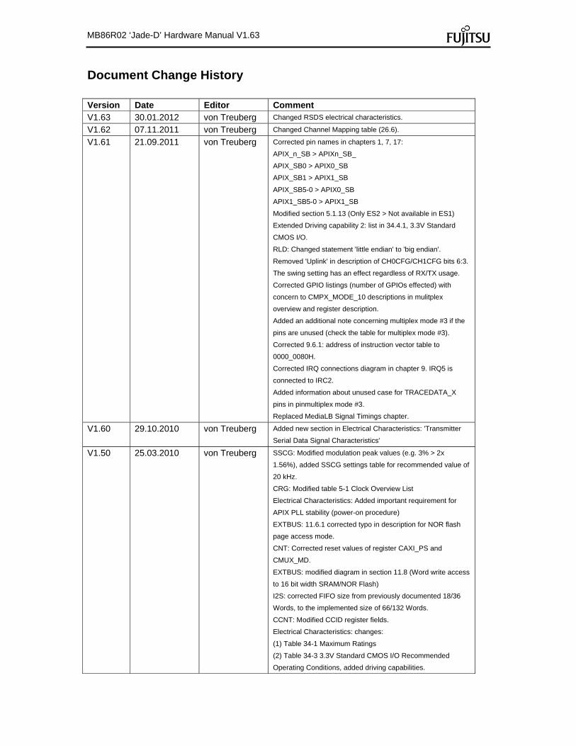
Document Change History
Version Date Editor Comment V1.63 30.01.2012 von Treuberg Changed RSDS electrical characteristics.
V1.62 07.11.2011 von Treuberg Changed Channel Mapping table (26.6).
V1.61 21.09.2011 von Treuberg Corrected pin names in chapters 1, 7, 17:
APIX_n_SB > APIXn_SB_
APIX_SB0 > APIX0_SB
APIX_SB1 > APIX1_SB
APIX_SB5-0 > APIX0_SB
APIX1_SB5-0 > APIX1_SB
Modified section 5.1.13 (Only ES2 > Not available in ES1)
Extended Driving capability 2: list in 34.4.1, 3.3V Standard
CMOS I/O.
RLD: Changed statement 'little endian' to 'big endian'.
Removed 'Uplink' in description of CH0CFG/CH1CFG bits 6:3.
The swing setting has an effect regardless of RX/TX usage.
Corrected GPIO listings (number of GPIOs effected) with
concern to CMPX_MODE_10 descriptions in mulitplex
overview and register description.
Added an additional note concerning multiplex mode #3 if the
pins are unused (check the table for multiplex mode #3).
Corrected 9.6.1: address of instruction vector table to
0000_0080H.
Corrected IRQ connections diagram in chapter 9. IRQ5 is
connected to IRC2.
Added information about unused case for TRACEDATA_X
pins in pinmultiplex mode #3.
Replaced MediaLB Signal Timings chapter.
V1.60 29.10.2010 von Treuberg Added new section in Electrical Characteristics: 'Transmitter
Serial Data Signal Characteristics'
V1.50 25.03.2010 von Treuberg SSCG: Modified modulation peak values (e.g. 3% > 2x
1.56%), added SSCG settings table for recommended value of
20 kHz.
CRG: Modified table 5-1 Clock Overview List
Electrical Characteristics: Added important requirement for
APIX PLL stability (power-on procedure)
EXTBUS: 11.6.1 corrected typo in description for NOR flash
page access mode.
CNT: Corrected reset values of register CAXI_PS and
CMUX_MD.
EXTBUS: modified diagram in section 11.8 (Word write access
to 16 bit width SRAM/NOR Flash)
I2S: corrected FIFO size from previously documented 18/36
Words, to the implemented size of 66/132 Words.
CCNT: Modified CCID register fields.
Electrical Characteristics: changes:
(1) Table 34-1 Maximum Ratings
(2) Table 34-3 3.3V Standard CMOS I/O Recommended
Operating Conditions, added driving capabilities.

MB86R02 ‘Jade-D’ Hardware Manual V1.63
(3) New section: APIX Characteristics
(4) Added RSDS characteristics
GDC: 18.6.3.3 Direct Color (24 bits/pixel) – corrected RGBA
table (A field is only 1 bit)
GDC: Extended all LxEC descriptions for RGBA (e.g. L1EC,
L2EC etc.)
RLD: byte alignment information added to StrideCfg1 register.
Limitations information added to AHBMTransferWidth Setup
section.
V1.40 19.10.2009 von Treuberg Overview: Unused pins - changed handling of OSC_FILTER,
changed handling of XTRST pin.
GPIO: re-inserted block diagram (mistakenly removed)
IRC: removed IRQs as only required for debugging
DMAC: Corrected line to MPX_MODE_1[1:0] = "HL" in section
'Related Pins'. Corrected DMA configuration A register
(DMACAx), BC[3:0] and TC[15:0] function descriptions.
RLD: added more detail to DestAddress register description
Electrical characteristics, almost all tables modified
CRG: corrected initial value of CRAM register.
TCON: exchanged Figure 22-4 Block diagram of TSIG.
SSCG: updated register description
UART: changed table 28-2:
(external input condition: CLK = 25.0MHz, CRIPM[3:0] = 0001)
Addendum (differences ES1/ES2): added note about APIX TX
initialization
V1.30 24.07.2009 von Treuberg CCNT: Corrected typo in description of register CAXI_PS
ADDENDUM: Added note about JTAGSEL polarity
DMAC: changed hex value in second diagram of section
'15.8.1 DMA start in Single channel'
GPIO: corrected base address in table 24-1
DDR2: several small corrections concerning DRIMRx and
OCD adjustment
CCNT: Added note that only 32 bit access to DDR is poss.
when in big endian mode. Extended description of multiplex
mode/function selection register CMUX_MD. Corrected ChipID
register displayed values.
Overview + Addendum: modified MUX tables for better
understanding. Added cell types to pin overview.
Memory map: changed RHlite to APIX, added SSCG area.
Modified Register Access description.
I2C: added 'Example of a slave address transmission'
GPIO: new block diagram and note about configuration of
differential pair configuration in MUX mode 4, function 4
SIG: added limitation for cyclic monitoring mode.
SSCG: added base address to register description.
CRG: modified description of DPERI register
V1.20 22.06.2009 von Treuberg CCNT: Page 9-12: corrected typo ADC7 > ADC2
GDC: VCCR register – changed reset value. Corrected table
of DCKD clock delay values and DCM3 description.
APIX: Changed names OscMode, OscBias, OscFilter to
OSC_MODE, OSC_BIAS and OSC_FILTER for consistancy. -

MB86R02 ‘Jade-D’ Hardware Manual V1.63
Added upstream channel bandwith limitation
IRC: Added info to IRQ7,8,19,20 ... 23: Unused, corresponding
correction to IRQ table (9.6)
EXTBUS: changed footnote of MCFMODE0/2/4
TCON: Removed superflous section concerning Indigo.
Exchanged block diagram of TSIG (22-4). Modified diagram
'Basic structure of a sync mixer (22-7).
DDR2: corrected flowchart and tables 13-4, 13-6, corrected
13.6.2.2 flow chart and added new explanation text. Added
limitation about read/write when in self-refresh mode.
Corrected 13.7.2.2 OCD Adjustment Procedure, changed
bitfield ODTBIAS in register DROABA.
SSCG: numerous small corrections. Removed references to
1.6 GHz operation (not for Jade-D implementation)
Addendum: added difference in SSCG functional scope
ES1/ES2
DMAC/I2S: added restriction for I2S transfer modes
SIG: Added new example control flow diagram to 21.6.1
Added new chapter 'Electrical Characteristics'
V1.10 18.05.2009 von Treuberg Overview: corrected bus connection information, added
improved overview of multiplex pin groups, corrected I2S unit
count, added section concerning PU/PD differences ES1/ES2,
updated pin listings/unused pins info
SPI: Added second channel
GDC: corrected display timing table values, added 1280 x 480
GDC: correcrected address offsets of L2WY, L2WW, L2WH
GDC: Modified DCM3 register
GDC: Added DCM1.LCS register description
GDC: Corrected RSDS bitfield initial value (DCM0 register)
CCNT: Renamed register CDEBUG0 > CBSC
CCNT: Renamed register CDEBUG1 > CDCRC
CCNT: Added new register CMSR2
CCNT: Corrected numbers of CMBUS register bitfields
CRG: Minimal register description changes
ADC: Corrected ADC channel mapping table, updated register
description
Added Addendum for differences ES1/ES2
IRC: Added missing registers for IRC2 to overview, corrected
TBR addresses in tables
CLUT: updated diagrams
DITH: updated diagrams
SIG: updated diagrams
TCON: updated diagrams
RLD: updated diagrams
V1.00 12.03.2009 von Treuberg Overview: Unused pins: changed handling of I2S_ECLK, VPD,
TDI, added information about internal pull-up/down resistors
for numerous pins, corrected number of IRC channels to 3.
GDC: corrected blending registers description
IRC: Removed IRC overview diagram (covered by tables)
Pin multiplex tables, changes to CMPX_MODE_2[1:0] and
CMPX_MODE_3[1:0] and CMPX_MODE_2[1:0].
MB86R02 ‘Jade-D’ Hardware Manual V1.63
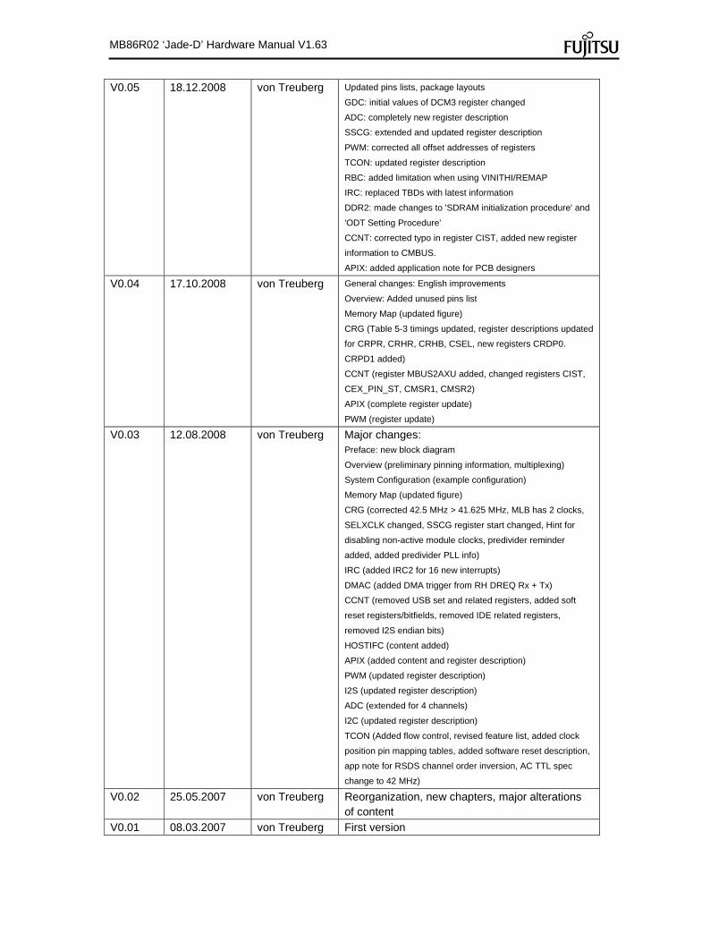
V0.05 18.12.2008 von Treuberg Updated pins lists, package layouts
GDC: initial values of DCM3 register changed
ADC: completely new register description
SSCG: extended and updated register description
PWM: corrected all offset addresses of registers
TCON: updated register description
RBC: added limitation when using VINITHI/REMAP
IRC: replaced TBDs with latest information
DDR2: made changes to 'SDRAM initialization procedure' and
'ODT Setting Procedure'
CCNT: corrected typo in register CIST, added new register
information to CMBUS.
APIX: added application note for PCB designers
V0.04 17.10.2008 von Treuberg General changes: English improvements
Overview: Added unused pins list
Memory Map (updated figure)
CRG (Table 5-3 timings updated, register descriptions updated
for CRPR, CRHR, CRHB, CSEL, new registers CRDP0.
CRPD1 added)
CCNT (register MBUS2AXU added, changed registers CIST,
CEX_PIN_ST, CMSR1, CMSR2)
APIX (complete register update)
PWM (register update)
V0.03 12.08.2008 von Treuberg Major changes: Preface: new block diagram Overview (preliminary pinning information, multiplexing)
System Configuration (example configuration)
Memory Map (updated figure)
CRG (corrected 42.5 MHz > 41.625 MHz, MLB has 2 clocks,
SELXCLK changed, SSCG register start changed, Hint for
disabling non-active module clocks, predivider reminder
added, added predivider PLL info)
IRC (added IRC2 for 16 new interrupts)
DMAC (added DMA trigger from RH DREQ Rx + Tx)
CCNT (removed USB set and related registers, added soft
reset registers/bitfields, removed IDE related registers,
removed I2S endian bits)
HOSTIFC (content added)
APIX (added content and register description)
PWM (updated register description)
I2S (updated register description)
ADC (extended for 4 channels)
I2C (updated register description)
TCON (Added flow control, revised feature list, added clock
position pin mapping tables, added software reset description,
app note for RSDS channel order inversion, AC TTL spec
change to 42 MHz)
V0.02 25.05.2007 von Treuberg Reorganization, new chapters, major alterations of content
V0.01 08.03.2007 von Treuberg First version

MB86R02 ‘Jade-D’ Hardware Manual V1.63
Table of Contents 1 Overview .................................................................................................................................... 1-1
1.1 Features ........................................................................................................................... 1-1 1.2 Block Diagram .................................................................................................................. 1-3
1.2.1 Outline of each functional block .................................................................................... 1-4 Function Summary of the Blocks .................................................................................................... 1-6 1.3 Package Dimensions ....................................................................................................... 1-9 1.4 Pinning ........................................................................................................................... 1-10 1.5 Pin Assignment .............................................................................................................. 1-10
1.5.1 Pin Assignment Table ................................................................................................. 1-12 1.5.2 Pin Multiplexing .......................................................................................................... 1-22
1.6 Pin Functional Description ............................................................................................. 1-31 2 System Configuration ................................................................................................................. 2-1
2.1 Typical Application ........................................................................................................... 2-1 3 Memory Map ............................................................................................................................... 3-1
3.1 Memory Map of LSI .......................................................................................................... 3-1 3.2 Register Access ............................................................................................................... 3-4
4 CPU (ARM926EJ-S core) ........................................................................................................... 4-1 4.1 Outline of ARM926EJ-S core ........................................................................................... 4-1 4.2 Features of ARM926EJ-S core ........................................................................................ 4-1 4.3 Block diagram of ARM926EJ-S core ................................................................................ 4-1 4.4 Configuration of ARM926EJ-S and ETM .......................................................................... 4-2
5 Clock Reset Generator (CRG) .................................................................................................... 5-1 5.1 Outline ............................................................................................................................. 5-1 5.2 Features ........................................................................................................................... 5-1 5.3 Overview .......................................................................................................................... 5-2 5.4 Location in the device ...................................................................................................... 5-3 5.5 Operation ......................................................................................................................... 5-3
5.5.1 Reset Generation ......................................................................................................... 5-3 5.5.2 Clock Generation .......................................................................................................... 5-7
5.6 Registers ........................................................................................................................ 5-16 5.1.1. Register list ................................................................................................................. 5-16 5.1.2. PLL control register (CRPR) ....................................................................................... 5-18 5.1.3. Watchdog timer control register (CRWR) ................................................................... 5-21 5.1.4. Reset/Standby control register (CRSR) ...................................................................... 5-23 5.1.5. Clock divider control register A (CRDA) ...................................................................... 5-25 5.1.6. Clock divider control register B (CRDB) ...................................................................... 5-27 5.1.7. AHB (A) bus clock gate control register (CRHA) ......................................................... 5-28 5.1.8. APB (A) bus clock gate control register (CRPA) ......................................................... 5-29 5.1.9. Reserved control register (CRPB) .............................................................................. 5-30 5.1.10. AHB (B) bus clock gate control register (CRHB) ..................................................... 5-31 5.1.11. ARM core clock gate control register (CRAM) ......................................................... 5-32 5.1.12. DPERI clock gate control register (CRDP0, CRDP1) .............................................. 5-32 5.1.13. Clock Selector control register (CSEL) .................................................................... 5-33
6 Spread Spectrum Clock Generator (SSCG) ............................................................................... 6-1 6.1 Position of Block in whole LSI .......................................................................................... 6-1 6.2 Features ........................................................................................................................... 6-1
6.2.1 Functional ..................................................................................................................... 6-1 6.2.2 Limitations .................................................................................................................... 6-1

MB86R02 ‘Jade-D’ Hardware Manual V1.63
6.3 Software Interface ............................................................................................................ 6-3 6.3.1 Format of Register Description ..................................................................................... 6-3 6.3.2 Global Address ............................................................................................................. 6-4 6.3.3 Register Summary ........................................................................................................ 6-4
Register Description ....................................................................................................................... 6-4 6.4 Processing Mode ............................................................................................................. 6-8
6.4.1 Parameter setting for 666MHz PLL clock ..................................................................... 6-8 6.4.1.1 Parameter setting for SSCG-speed of 15KHz ....................................................... 6-8 6.4.1.2 Parameter setting for SSCG-speed of 20KHz ....................................................... 6-9 6.4.1.3 Parameter setting for SSCG-speed of 35KHz ..................................................... 6-10 6.4.1.4 Parameter setting for SSCG-speed of 50KHz ..................................................... 6-10
6.5 Control Flow ................................................................................................................... 6-11 6.5.1 Operation.................................................................................................................... 6-11
7 CCNT (Chip Control) .................................................................................................................. 7-1 7.1 Overview .......................................................................................................................... 7-1 7.2 Features ........................................................................................................................... 7-2 7.3 Supply clock ..................................................................................................................... 7-2 7.4 Registers .......................................................................................................................... 7-3
7.4.1 Register list ................................................................................................................... 7-3 7.4.2 CHIP ID register (CCID) ............................................................................................... 7-5 7.4.3 Soft reset register (CSRST) .......................................................................................... 7-6 7.4.4 Interrupt status register (CIST) ..................................................................................... 7-7 7.4.5 Interrupt status mask register (CISTM) ......................................................................... 7-9 7.4.6 GPIO interrupt status register (CGPIO_IST) ............................................................... 7-11 7.4.7 GPIO interrupt status mask register (CGPIO_ISTM) .................................................. 7-11 7.4.8 GPIO interrupt polarity setting register (CGPIO_IP) ................................................... 7-13 7.4.9 GPIO interrupt mode setting register (CGPIO_IM) ..................................................... 7-13 7.4.10 AXI bus wait cycle set register (CAXI_BW) ................................................................ 7-15 7.4.11 AXI priority setting register (CAXI_PS) ....................................................................... 7-17 7.4.12 Multiplex mode setting register (CMUX_MD) .............................................................. 7-19 7.4.13 External pin status register (CEX_PIN_ST) ................................................................ 7-21 7.4.14 MediaLB set register (CMLB) ..................................................................................... 7-22 7.4.15 MBUS2AXU set register (CMBUS) ............................................................................. 7-24 7.4.16 Mode switch register like endian etc. (CBSC) ............................................................. 7-25 7.4.17 DDR2 Interface reset control register (CDCRC) ......................................................... 7-27 7.4.18 Soft reset register 0 for macro (CMSR0) .................................................................... 7-28 7.4.19 Soft reset register 1 for macro (CMSR1) .................................................................... 7-30 7.4.20 Soft reset register 2 for macro (CMSR2) .................................................................... 7-33
8 Remap Boot Controller (RBC) .................................................................................................... 8-1 8.1 Outline ............................................................................................................................. 8-1 8.2 Features ........................................................................................................................... 8-1 8.3 Block Diagram .................................................................................................................. 8-1 8.4 Supply clock ..................................................................................................................... 8-2 8.5 Register ........................................................................................................................... 8-2
8.5.1 Register list ................................................................................................................... 8-2 8.5.2 Remap control register (RBREMAP) ............................................................................ 8-4 8.5.3 VINITHI control register A (RBVIHA) ............................................................................ 8-5 8.5.4 INITRAM control register A (RBITRA) .......................................................................... 8-6
8.6 Operation ......................................................................................................................... 8-7 8.6.1 RBC reset ..................................................................................................................... 8-7 8.6.2 Remap control .............................................................................................................. 8-7 8.6.3 VINITHI control ............................................................................................................. 8-7

MB86R02 ‘Jade-D’ Hardware Manual V1.63
8.6.4 INITRAM control ........................................................................................................... 8-9 9 Interrupt Request Controller (IRC) .............................................................................................. 9-1
9.1 Overview .......................................................................................................................... 9-1 9.2 Features ........................................................................................................................... 9-1 9.3 Interrupt map .................................................................................................................... 9-2
9.3.1 Exception vector to ARM926EJ-S core ......................................................................... 9-2 9.3.2 Expansion IRQ interrupt vector of IRC0/IRC1 ............................................................... 9-3 9.3.3 Interrupt request connection diagram ........................................................................... 9-6
9.4 Block diagram .................................................................................................................. 9-7 9.5 Register ........................................................................................................................... 9-8
9.5.1 Register list ................................................................................................................... 9-8 9.5.2 IRQ flag register (IRQF) ............................................................................................. 9-15 9.5.3 IRQ mask register (IRQM) .......................................................................................... 9-16 9.5.4 Interrupt level mask register (ILM) .............................................................................. 9-16 9.5.5 ICR monitoring register (ICRMN) ................................................................................ 9-18 9.5.6 Holding request cancellation level register (HRCL) .................................................... 9-19 9.5.7 Delay interrupt control register (DICR) ........................................................................ 9-20 9.5.8 Table base register (TBR) .......................................................................................... 9-21 9.5.9 Interrupt vector register (VCT) .................................................................................... 9-22 9.5.10 IRQ test register (IRQTEST) ....................................................................................... 9-23 9.5.11 FIQ test register (FIQTEST) ....................................................................................... 9-24 9.5.12 Interrupt control register (ICR31-ICR00) ..................................................................... 9-25
9.6 Operation explanation .................................................................................................... 9-27 9.6.1 Outline of operation .................................................................................................... 9-27 9.6.2 Initialization ................................................................................................................. 9-27 9.6.3 Multiple interrupt processing ....................................................................................... 9-28 9.6.4 Example of IRQ interrupt handler ............................................................................... 9-28 9.6.5 Stop and return from sleep mode ............................................................................... 9-30 9.6.6 Notes on use of IRC ................................................................................................... 9-31
10 External Interrupt Controller (EXIRC) .................................................................................... 10-1 10.1 Outline ........................................................................................................................... 10-1 10.2 Feature .......................................................................................................................... 10-1 10.3 Block diagram ................................................................................................................ 10-2 10.4 Supply clock ................................................................................................................... 10-2 10.5 Register ......................................................................................................................... 10-3
10.5.1 Register list ................................................................................................................. 10-3 10.5.2 External interrupt enable register (EIENB) .................................................................. 10-5 10.5.3 External interrupt request register (EIREQ) ................................................................ 10-6 10.5.4 External interrupt level register (EILVL) ...................................................................... 10-7
10.6 Operation ....................................................................................................................... 10-8 10.7 Operation procedure ...................................................................................................... 10-8 10.8 Instruction for use .......................................................................................................... 10-8
11 External Bus Interface ........................................................................................................... 11-1 11.1 Outline ........................................................................................................................... 11-1 11.2 Features ......................................................................................................................... 11-1 11.3 Block diagram ................................................................................................................ 11-1 11.4 Related pin ..................................................................................................................... 11-2 11.5 Supply clock ................................................................................................................... 11-2 11.6 Register ......................................................................................................................... 11-3
11.6.1 SRAM/Flash mode register 0/2/4 (MCFMODE0/2/4) .................................................. 11-3 11.6.2 SRAM/Flash timing register 0/2/4 (MCFTIM0/2/4) ...................................................... 11-5 11.6.3 SRAM/Flash area register 0/2/4 (MCFAREA0/2/4) ..................................................... 11-8

MB86R02 ‘Jade-D’ Hardware Manual V1.63
11.6.4 Memory controller error register (MCERR) ............................................................... 11-11 11.7 Connection example .................................................................................................... 11-12 11.8 Example of access waveform ....................................................................................... 11-13 11.9 Operation ..................................................................................................................... 11-17
11.9.1 External bus interface ............................................................................................... 11-17 11.9.2 Low-speed device interface function......................................................................... 11-17 11.9.3 Endian and byte lane to each access ....................................................................... 11-18
12 Embedded SRAM ................................................................................................................. 12-1 12.1 Outline ........................................................................................................................... 12-1 12.2 Features ......................................................................................................................... 12-1 12.3 Block diagram ................................................................................................................ 12-1 12.4 Supply clock ................................................................................................................... 12-1
13 DDR2 Controller .................................................................................................................... 13-1 13.1 Outline ........................................................................................................................... 13-1 13.2 Features ......................................................................................................................... 13-1 13.3 Limitation ....................................................................................................................... 13-1 13.4 Block Diagram ................................................................................................................ 13-2 13.5 Supply Clock .................................................................................................................. 13-3 13.6 Registers ........................................................................................................................ 13-3
13.6.1 Register List ............................................................................................................... 13-3 13.6.2 DRAM initialization control register (DRIC) ................................................................. 13-5 13.6.3 DRAM initialization command register [1] (DRIC1) ..................................................... 13-7 13.6.4 DRAM initialization command register [2] (DRIC2) ..................................................... 13-7 13.6.5 DRAM CTRL ADD register (DRCA) ............................................................................ 13-8 13.6.6 DRAM control mode register (DRCM) ........................................................................ 13-9 13.6.7 DRAM CTRL SET TIME1 Register (DRCST1) ......................................................... 13-10 13.6.8 DRAM CTRL SET TIME2 register (DRCST2) ........................................................... 13-12 13.6.9 DRAM CTRL REFRESH register (DRCR) ................................................................ 13-14 13.6.10 DRAM CTRL FIFO register (DRCF) ...................................................................... 13-15 13.6.11 AXI setting register (DRASR) ................................................................................ 13-16 13.6.12 DRAM IF MACRO SETTING DLL register (DRIMSD) ........................................... 13-17 13.6.13 DRAM ODT SETTING register (DROS) ................................................................ 13-18 13.6.14 IO buffer setting ODT1 (DRIBSODT1) .................................................................. 13-19 13.6.15 IO buffer setting OCD (DRIBSOCD) ..................................................................... 13-20 13.6.16 IO buffer setting OCD2 (DRIBSOCD2) ................................................................. 13-21 13.6.17 ODT auto bias adjust register (DROABA) ............................................................. 13-22 13.6.18 ODT bias select register (DROBS) ........................................................................ 13-23 13.6.19 IO monitor register 1 (DRIMR1) ............................................................................ 13-24 13.6.20 IO monitor register 2 (DRIMR2) ............................................................................ 13-24 13.6.21 IO monitor register 3 (DRIMR3) ............................................................................ 13-25 13.6.22 IO monitor register 4 (DRIMR4) ............................................................................ 13-25 13.6.23 OCD impedance setting register 1 (DROISR1) ..................................................... 13-26 13.6.24 OCD impedance setting register 2 (DROISR2) ..................................................... 13-26
13.7 Operation ..................................................................................................................... 13-27 13.7.1 DRAM Initialization Sequence .................................................................................. 13-27 13.7.2 DRAM Initialization Procedure .................................................................................. 13-28
13.7.2.1 SDRAM Initialization Procedure ........................................................................ 13-30 13.7.2.2 OCD Adjustment Procedure .............................................................................. 13-33 13.7.2.3 ODT Setting Procedure ..................................................................................... 13-35
14 Timer (TIMER) ...................................................................................................................... 14-1 14.1 Outline ........................................................................................................................... 14-1 14.2 Feature .......................................................................................................................... 14-1
MB86R02 ‘Jade-D’ Hardware Manual V1.63
14.3 Supply clock ................................................................................................................... 14-1 14.4 Specification ................................................................................................................... 14-1
15 DMA Controller (DMAC) ........................................................................................................ 15-1 15.1 Outline ........................................................................................................................... 15-1 15.2 Feature .......................................................................................................................... 15-1 15.3 Block diagram ................................................................................................................ 15-2 15.4 Related pins ................................................................................................................... 15-3 15.5 Supply clock ................................................................................................................... 15-3 15.6 Registers ........................................................................................................................ 15-4
15.6.1 Register list ................................................................................................................. 15-4 15.6.2 DMA configuration register (DMACR) ......................................................................... 15-6 15.6.3 DMA configuration A register (DMACAx) .................................................................... 15-8 15.6.4 DMA configuration B register (DMACBx) .................................................................. 15-11 15.6.5 DMAC source address register (DMACSAx) ............................................................ 15-14 15.6.6 DMAC destination address register (DMACDAx) ...................................................... 15-15
15.7 Operation ..................................................................................................................... 15-16 15.7.1 Transfer modes ........................................................................................................ 15-16
15.7.1.1 Block transfer .................................................................................................... 15-16 15.7.1.2 Limitations with I2S DMA ................................................................................... 15-20 15.7.1.3 Burst transfer ..................................................................................................... 15-21 15.7.1.4 Demand transfer ................................................................................................ 15-25
15.7.2 Beat transfer ............................................................................................................. 15-29 15.7.2.1 Normal and Single transfer ................................................................................ 15-29 15.7.2.2 Increment and lap transfer ................................................................................. 15-30
15.7.3 Channel priority control ............................................................................................. 15-31 15.7.3.1 Fixed priority ...................................................................................................... 15-31 15.7.3.2 Rotate priority .................................................................................................... 15-32
15.7.4 Retry, split, and error ................................................................................................ 15-33 15.7.4.1 Retry and split ................................................................................................... 15-33 15.7.4.2 Error .................................................................................................................. 15-34
15.8 DMAC Configuration Examples .................................................................................... 15-35 15.8.1 DMA start in Single channel ..................................................................................... 15-35 15.8.2 DMA start in all channels (in demand transfer mode) ............................................... 15-36
16 Host Interface ........................................................................................................................ 16-1 16.1. Outline ........................................................................................................................... 16-1 16.2. Features ......................................................................................................................... 16-1
16.2.1. Features .................................................................................................................. 16-1 16.2.2. Limitations ............................................................................................................... 16-1
16.3. Function ......................................................................................................................... 16-2 16.3.1. Block Diagram ........................................................................................................ 16-2 16.3.2. SPI Interface ........................................................................................................... 16-2
16.3.2.1. Write Access ....................................................................................................... 16-2 16.3.2.2. Read Access ....................................................................................................... 16-4
16.3.3. Interrupt .................................................................................................................. 16-6 16.3.3.1. AHB slave module access error response ........................................................... 16-6
16.3.4. Reset Request ........................................................................................................ 16-6 16.4. External Interfaces ......................................................................................................... 16-7
16.4.1. Communication Protocols (Timing Diagrams) ......................................................... 16-7 16.4.1.1. SPI protocol stack ............................................................................................... 16-7
16.4.2. Data Formats .......................................................................................................... 16-8 16.4.2.1. Host Interface (clock timing and phase)............................................................... 16-8 16.4.2.2. Reset Frame........................................................................................................ 16-8
MB86R02 ‘Jade-D’ Hardware Manual V1.63
16.4.2.3. Signal input format from the host CPU ................................................................ 16-8 16.5. Application Notes ......................................................................................................... 16-10
16.5.1. Processing Flow.................................................................................................... 16-10 16.5.1.1. Begin timing of protocol sequence ..................................................................... 16-10 16.5.1.2. Receive operation and the STATUS byte .......................................................... 16-10 16.5.1.3. Setting the address ........................................................................................... 16-10 16.5.1.4. Handling of irregular operating conditions ......................................................... 16-11
17 APIX® Interface .................................................................................................................... 17-1 17.1 Outline ........................................................................................................................... 17-1 17.2 Features ......................................................................................................................... 17-1
17.2.1.1 APIX® PHY ......................................................................................................... 17-1 17.2.1.2 APIX® Ashell ....................................................................................................... 17-1 17.2.1.3 Jade-D Restrictions ............................................................................................. 17-2
17.2.2 Block diagram ............................................................................................................. 17-3 17.3 Software Interface .......................................................................................................... 17-4
17.3.1 Format of Register Description ................................................................................... 17-4 17.3.2 Global Address ........................................................................................................... 17-4 17.3.3 Register Summary ...................................................................................................... 17-5 17.3.4 Register Description ................................................................................................... 17-6
17.4 Description of APIX Ashell and APIX PHY configuration bytes .................................... 17-16 17.4.1 RX ............................................................................................................................ 17-16 17.4.2 TX ............................................................................................................................. 17-26
17.5 GPIO Interface Timing of Sideband Uplink and Downlink ............................................ 17-38 17.6 Control Flow ................................................................................................................. 17-39
17.6.1 Use cases ................................................................................................................. 17-40 17.6.1.1 Use case 1 ........................................................................................................ 17-40 17.6.1.2 Use case 2 ........................................................................................................ 17-42
17.6.2 Application Notes for PCB Designers ....................................................................... 17-44 18 Graphics Display Controller (GDC) ....................................................................................... 18-1
18.1 Preface .......................................................................................................................... 18-1 18.2 Features ......................................................................................................................... 18-1 18.3 Functional Overview....................................................................................................... 18-2
18.3.1 Display controller ........................................................................................................ 18-2 18.3.2 Video capture function ................................................................................................ 18-4 18.3.3 Geometry processing ................................................................................................. 18-4 18.3.4 2D Drawing ................................................................................................................. 18-5 18.3.5 3D Drawing ................................................................................................................. 18-7 18.3.6 Special effects ............................................................................................................ 18-8 18.3.7 Others ...................................................................................................................... 18-10
18.4 Graphics Memory ......................................................................................................... 18-11 18.4.1 Memory map ............................................................................................................ 18-11 18.4.2 Configuration ............................................................................................................ 18-12 18.4.3 Data Type ................................................................................................................. 18-12 18.4.4 Data Format ............................................................................................................. 18-13
18.5 Frame Management ..................................................................................................... 18-15 18.5.1 Single Buffer ............................................................................................................. 18-15 18.5.2 Double Buffer ........................................................................................................... 18-15
18.6 Display Controller ......................................................................................................... 18-16 18.6.1 Overview .................................................................................................................. 18-16 18.6.2 Display Function ....................................................................................................... 18-17
18.6.2.1 Layer configuration ............................................................................................ 18-17 18.6.2.2 Overlay .............................................................................................................. 18-18

MB86R02 ‘Jade-D’ Hardware Manual V1.63
18.6.2.3 Display parameters ........................................................................................... 18-20 18.6.2.4 Display position control ...................................................................................... 18-21
18.6.3 Display Color ............................................................................................................ 18-23 18.6.3.1 Indirect Color (8 bits/pixel) ................................................................................. 18-23 18.6.3.2 Direct Color (16 bits/pixel) ................................................................................. 18-23 18.6.3.3 Direct Color (24 bits/pixel) ................................................................................. 18-23 18.6.3.4 YCbCr Color (16 bits/pixel) ................................................................................ 18-24 18.6.3.5 Alpha factor (8 bits/pixel) ................................................................................... 18-24 18.6.3.6 Layer dependence ............................................................................................. 18-24
18.6.4 Cursor ...................................................................................................................... 18-25 18.6.4.1 Cursor display function ...................................................................................... 18-25 18.6.4.2 Cursor control .................................................................................................... 18-25
18.6.5 Display Scan Control ................................................................................................ 18-25 18.6.5.1 Applicable display .............................................................................................. 18-25 18.6.5.2 Interlace display ................................................................................................ 18-26
18.6.6 Programmable YCbCr/RGB conversion for L1-layer display .................................... 18-27 18.6.7 DCLKO shift ............................................................................................................. 18-29 18.6.8 Synchronous register updates and display ............................................................... 18-29 18.6.9 Parallel Dual Display ................................................................................................ 18-30 18.6.10 Multiplex Dual Display ........................................................................................... 18-31
18.6.10.1 Overview .......................................................................................................... 18-31 18.6.10.2 Destination Control ........................................................................................... 18-31 18.6.10.3 Output Signal Control ....................................................................................... 18-32 18.6.10.4 Output Circuit Example ..................................................................................... 18-32 18.6.10.5 Display Clock and Timing ................................................................................. 18-34 18.6.10.6 Limitations ........................................................................................................ 18-34 18.6.10.7 Dual display configuration example .................................................................. 18-34
18.6.11 Video output limitation ........................................................................................... 18-35 18.6.12 Interrupt ................................................................................................................ 18-35
18.7 Video Capture .............................................................................................................. 18-37 18.7.1 Video Capture function ............................................................................................. 18-37
18.7.1.1 Input data Formats ............................................................................................ 18-37 18.7.1.2 Video Signal Capture ........................................................................................ 18-37 18.7.1.3 Non-interlace Transformation ............................................................................ 18-37
18.7.2 Input Port Selection .................................................................................................. 18-38 18.7.3 Video Buffer .............................................................................................................. 18-40
18.7.3.1 Data Format ...................................................................................................... 18-40 18.7.3.2 Synchronization Control .................................................................................... 18-41 18.7.3.3 Area Allocation .................................................................................................. 18-41 18.7.3.4 Window Display ................................................................................................. 18-41 18.7.3.5 Interlaced Display .............................................................................................. 18-42
18.7.4 Scaling ..................................................................................................................... 18-43 18.7.4.1 Downscaling Function ....................................................................................... 18-43 18.7.4.2 Upscaling Function ............................................................................................ 18-43 18.7.4.3 Flow of image processing .................................................................................. 18-45
18.7.5 External video signal input conditions ....................................................................... 18-48 18.7.5.1 RTB656 YUV422 input format ........................................................................... 18-48 18.7.5.2 RGB input format ............................................................................................... 18-50 18.7.5.3 Input Operation .................................................................................................. 18-51 18.7.5.4 Conversion Operation........................................................................................ 18-53
18.7.6 Display Controller / Video Capture Register Summary ............................................. 18-55 18.7.6.1 Common Control Registers ............................................................................... 18-55

MB86R02 ‘Jade-D’ Hardware Manual V1.63
18.7.6.2 Display Controller Registers .............................................................................. 18-55 18.7.6.3 Video capture registers ...................................................................................... 18-61
18.7.7 Explanation of Local Memory Registers ................................................................... 18-63 18.7.8 Common control register .......................................................................................... 18-64 18.7.9 Display control register ............................................................................................. 18-66 18.7.10 Video capture registers ....................................................................................... 18-121
18.8 Timing Diagrams ........................................................................................................ 18-138 18.8.1 Display Timing Diagram ......................................................................................... 18-138
18.8.1.1 Non-interlace mode ......................................................................................... 18-138 18.8.1.2 Interlace video mode ....................................................................................... 18-140
18.8.2 Composite synchronous signal ............................................................................... 18-141 18.9 Geometry Engine ....................................................................................................... 18-142
18.9.1 Geometry Pipeline .................................................................................................. 18-142 18.9.1.1 Processing flow ............................................................................................... 18-142 18.9.1.2 Model-view-projection (MVP) transformation ................................................... 18-143 18.9.1.3 3D-2D transformation (CCNDC coordinate transformation) ......................... 18-143 18.9.1.4 View port transformation (NDCDC coordinate transformation) ..................... 18-144 18.9.1.5 View volume clipping ....................................................................................... 18-144 18.9.1.6 Back face culling ............................................................................................. 18-146
18.9.2 Data Format ........................................................................................................... 18-147 18.9.2.1 Data format ..................................................................................................... 18-147 18.9.2.2 Setup processing ............................................................................................. 18-148
18.9.3 Log Output of Device Coordinates .......................................................................... 18-148 18.9.3.1 Log output mode ............................................................................................. 18-148 18.9.3.2 Log output destination address........................................................................ 18-148 18.9.3.3 Log output format ............................................................................................ 18-148
18.10 Drawing Processing ................................................................................................... 18-149 18.10.1 Coordinate System ............................................................................................. 18-149
18.10.1.1 Drawing coordinates ....................................................................................... 18-149 18.10.1.2 Texture coordinates ........................................................................................ 18-150 18.10.1.3 Frame buffer ................................................................................................... 18-150
18.10.2 Figure Drawing ................................................................................................... 18-151 18.10.2.1 Drawing primitives .......................................................................................... 18-151 18.10.2.2 Polygon drawing function ............................................................................... 18-151 18.10.2.3 Drawing parameters ....................................................................................... 18-152 18.10.2.4 Anti-aliasing function ...................................................................................... 18-153
18.10.3 Bit Map Processing ............................................................................................. 18-154 18.10.3.1 BLT ................................................................................................................. 18-154 18.10.3.2 Pattern data format ......................................................................................... 18-154
18.10.4 Texture Mapping ................................................................................................. 18-155 18.10.4.1 Texture size .................................................................................................... 18-155 18.10.4.2 Texture color .................................................................................................. 18-155 18.10.4.3 Texture Wrapping ........................................................................................... 18-156 18.10.4.4 Filtering .......................................................................................................... 18-157 18.10.4.5 Perspective correction .................................................................................... 18-157 18.10.4.6 Texture blending ............................................................................................. 18-158 18.10.4.7 Bi-linear high-speed mode .............................................................................. 18-158
18.10.5 Rendering ........................................................................................................... 18-160 18.10.5.1 Tiling ............................................................................................................... 18-160 18.10.5.2 Alpha blending ................................................................................................ 18-160 18.10.5.3 Logic operation ............................................................................................... 18-161 18.10.5.4 Hidden plane management ............................................................................ 18-161
MB86R02 ‘Jade-D’ Hardware Manual V1.63
18.10.6 Drawing Attributes ............................................................................................... 18-162 18.10.6.1 Line drawing attributes ................................................................................... 18-162 18.10.6.2 Triangle drawing attributes ............................................................................. 18-162 18.10.6.3 Texture attributes ........................................................................................... 18-163 18.10.6.4 BLT attributes ................................................................................................. 18-164 18.10.6.5 Character pattern drawing attributes .............................................................. 18-164
18.10.7 Bold Line ............................................................................................................. 18-164 18.10.7.1 Starting and ending points .............................................................................. 18-164 18.10.7.2 Broken line pattern ......................................................................................... 18-165 18.10.7.3 Edging ............................................................................................................ 18-166 18.10.7.4 Interpolation of bold line joint .......................................................................... 18-167
18.10.8 Shadowing .......................................................................................................... 18-168 18.10.8.1 Shadowing ..................................................................................................... 18-168
18.11 Display Lists ............................................................................................................... 18-168 18.11.1 Overview ............................................................................................................. 18-168
18.11.1.1 Header format ................................................................................................ 18-170 18.11.1.2 Parameter format ........................................................................................... 18-170
18.11.2 Geometry Commands ......................................................................................... 18-171 18.11.2.1 Geometry command list .................................................................................. 18-171 18.11.2.2 Explanation of geometry commands .............................................................. 18-175
18.11.3 Rendering Commands ........................................................................................ 18-184 18.11.3.1 Command list ................................................................................................. 18-184 18.11.3.2 Details of rendering commands ...................................................................... 18-189
18.11.4 Drawing Engine / Geometry Engine Register summary ...................................... 18-199 18.11.4.1 Drawing Engine register list ............................................................................ 18-199 18.11.4.2 Geometry Engine register list ......................................................................... 18-206
18.11.5 Drawing control registers .................................................................................... 18-207 18.11.6 Drawing mode registers ...................................................................................... 18-210 18.11.7 Triangle drawing registers ................................................................................... 18-228 18.11.8 Line drawing registers ......................................................................................... 18-231 18.11.9 Pixel drawing registers ........................................................................................ 18-232 18.11.10 Rectangle drawing registers ................................................................................ 18-232 18.11.11 Blt registers ......................................................................................................... 18-233 18.11.12 High-speed 2D line drawing registers ................................................................. 18-234 18.11.13 High-speed 2D triangle drawing registers ........................................................... 18-235 18.11.14 Geometry control register .................................................................................... 18-236 18.11.15 Geometry mode registers .................................................................................... 18-238 18.11.16 Display list FIFO registers ................................................................................... 18-245 18.11.17 Display List DMA contol registers ....................................................................... 18-246
18.11.17.1 Display List DMA contol register list ............................................................. 18-246 18.11.18 Interrupt registers ................................................................................................ 18-249
18.11.18.1 Interrupt register list ...................................................................................... 18-249 19 Color Lookup Table (CLUT) .................................................................................................. 19-1
19.1 Color LUT ...................................................................................................................... 19-1 19.1.1 Overview .................................................................................................................... 19-1 19.1.2 Features ..................................................................................................................... 19-1 19.1.3 Position of the CLUT .................................................................................................. 19-2
19.2 Software Interface .......................................................................................................... 19-3 19.2.1 Format of Register Description ................................................................................... 19-3 19.2.2 Global Address ........................................................................................................... 19-3 19.2.3 Register Summary ...................................................................................................... 19-3 19.2.4 Register Description ................................................................................................... 19-4
MB86R02 ‘Jade-D’ Hardware Manual V1.63
19.3 Limitations ...................................................................................................................... 19-4 19.4 Initialization procedure ................................................................................................... 19-4
20 Dither Unit ............................................................................................................................. 20-1 20.1 Overview ........................................................................................................................ 20-1
20.1.1 Features ..................................................................................................................... 20-1 20.1.2 Position ...................................................................................................................... 20-2 20.1.3 Timing chart ................................................................................................................ 20-3
20.2 Software Interface .......................................................................................................... 20-4 20.2.1 Format of Register Description ................................................................................... 20-4 20.2.2 Global Address ........................................................................................................... 20-4 20.2.3 Register Summary ...................................................................................................... 20-4 20.2.4 Register Description ................................................................................................... 20-4
20.3 Limitations ...................................................................................................................... 20-5 20.4 Initialization procedure ................................................................................................... 20-5
21 Signature Generator (SIG) .................................................................................................... 21-1 21.1 Position of Block in whole LSI ........................................................................................ 21-1 21.2 Overview ........................................................................................................................ 21-1 21.3 Feature List .................................................................................................................... 21-1
21.3.1 Signature A: CRC-32 Signature .................................................................................. 21-2 21.3.2 Signature B: Summation Signature ............................................................................ 21-2 21.3.3 Programmable Evaluation Window (Position and Size) .............................................. 21-2 21.3.4 Programmable Evaluation Window Mask ................................................................... 21-2 21.3.5 Automatic Monitoring and Interrupt ............................................................................. 21-2 21.3.6 Self Restoring Error Counter ...................................................................................... 21-2 21.3.7 Interrupts For Control Flow ......................................................................................... 21-2 21.3.8 Programmable Input Picture Source ........................................................................... 21-2 21.3.9 Limitations .................................................................................................................. 21-3
21.4 Software Interface .......................................................................................................... 21-3 21.4.1 Format of Register Description ................................................................................... 21-3 21.4.2 Global Address ........................................................................................................... 21-4 21.4.3 Register Summary ...................................................................................................... 21-4 21.4.4 Register Description ................................................................................................... 21-5
21.5 Processing Mode ......................................................................................................... 21-12 21.5.1 Processing Flow ....................................................................................................... 21-12 21.5.2 Processing Algorithm ................................................................................................ 21-12
21.6 Control Flow ................................................................................................................. 21-13 21.6.1 Example Control Flow .............................................................................................. 21-13 21.6.2 Signature Generation with every incoming frame ..................................................... 21-15 21.6.3 Cyclic Signature Generation with every incoming frame ........................................... 21-15 21.6.4 Cyclic Signature Generation with every incoming frame, limiting read accesses ...... 21-16 21.6.5 Limitation of Cyclic Signature Generation ................................................................. 21-16
22 Timing Controller (TCON) ..................................................................................................... 22-1 22.1 Position of Block in whole LSI ........................................................................................ 22-1 22.2 Overview ........................................................................................................................ 22-1 22.3 Feature List .................................................................................................................... 22-1 22.4 Software Interface .......................................................................................................... 22-3 22.5 Processing Mode ......................................................................................................... 22-29
22.5.1 Processing Flow ....................................................................................................... 22-29 22.5.2 Processing Algorithm ................................................................................................ 22-29
22.5.2.1 Operation Modes ............................................................................................... 22-29 22.5.2.2 SW Reset .......................................................................................................... 22-30 22.5.2.3 RSDS Bitmap Mdule (RBM) .............................................................................. 22-30

MB86R02 ‘Jade-D’ Hardware Manual V1.63
22.5.2.4 Timing Signal Module (TSIG) ............................................................................ 22-32 22.5.2.5 Inversion Signal Generation .............................................................................. 22-37 22.5.2.6 Bypass-Mode .................................................................................................... 22-38 22.5.2.7 AC Characteristics ............................................................................................. 22-39
22.5.3 Limitations ................................................................................................................ 22-41 22.6 Application Note ........................................................................................................... 22-42
22.6.1.1 Channel to pin mapping ..................................................................................... 22-42 22.6.1.2 Pin mapping RSDS ........................................................................................... 22-42 22.6.1.3 Pin mapping TTL ............................................................................................... 22-42
22.6.2 Example Control Flow ................................................................................................ 22-1 23 Run-Length Decompression (RLD) ....................................................................................... 23-1
23.1 Position of Block in whole LSI ........................................................................................ 23-1 23.1.1 Data Flow in the LSI ................................................................................................... 23-1
23.2 Overview ........................................................................................................................ 23-2 23.3 Feature List .................................................................................................................... 23-2
23.3.1 References ................................................................................................................. 23-2 23.3.2 Integration and Application Hints ................................................................................ 23-2
23.3.2.1 Usage of RLD with Jade-D .................................................................................. 23-2 23.4 Communication Protocols (Timing Diagrams) ................................................................ 23-2
23.4.1 Result Interface .......................................................................................................... 23-2 23.4.2 Configuration Bus Interface ........................................................................................ 23-2 23.4.3 Interrupt ...................................................................................................................... 23-2
23.5 Data Formats ................................................................................................................. 23-3 23.5.1.1 Input Data Format ............................................................................................... 23-3 23.5.1.2 Output Data Format ............................................................................................. 23-4
23.6 Software Interface .......................................................................................................... 23-4 23.6.1 Format of Register Description ................................................................................... 23-4 23.6.2 Global Address ........................................................................................................... 23-5 23.6.3 Register Summary ...................................................................................................... 23-5 23.6.4 Register Description ................................................................................................... 23-6
23.7 Processing Mode ........................................................................................................... 23-9 23.7.1 Processing Flow ......................................................................................................... 23-9 23.7.2 Processing Algorithm .................................................................................................. 23-9
23.7.2.1 Processing Modes ............................................................................................... 23-9 23.8 Control Flow ................................................................................................................... 23-9
23.8.1 Example Control Flow ................................................................................................ 23-9 23.9 Limitations .................................................................................................................... 23-10
23.9.1 AHBMTransferWidth Setup ...................................................................................... 23-10 24 General-Purpose Input/Output Port (GPIO)........................................................................... 24-1
24.1 Outline ........................................................................................................................... 24-1 24.2 Feature .......................................................................................................................... 24-1 24.3 Block diagram ................................................................................................................ 24-1 24.4 Supply clock ................................................................................................................... 24-2 24.5 Limitations ...................................................................................................................... 24-2 24.6 Register ......................................................................................................................... 24-3
24.6.1 Register list ................................................................................................................. 24-3 24.6.2 Port data register 0-2 (GPDR0-2) ............................................................................... 24-5 24.6.3 Data direction register 0-2 (GPDDR0-2) ..................................................................... 24-7
24.7 Operation ....................................................................................................................... 24-9 24.7.1 Direction control ......................................................................................................... 24-9 24.7.2 Data transfer ............................................................................................................... 24-9
25 Pulse Width Modulator (PWM) .............................................................................................. 25-1

MB86R02 ‘Jade-D’ Hardware Manual V1.63
25.1 Outline ........................................................................................................................... 25-1 25.2 Feature .......................................................................................................................... 25-1 25.3 Block diagram ................................................................................................................ 25-2 25.4 Related pins ................................................................................................................... 25-2 25.5 Clock Supply .................................................................................................................. 25-2 25.6 Interrupts ........................................................................................................................ 25-2 25.7 Registers ........................................................................................................................ 25-3
25.7.1 Register list ................................................................................................................. 25-3 25.7.2 PWMx base clock register (PWMxBCR) ..................................................................... 25-5 25.7.3 PWMx pulse width register (PWMxTPR) .................................................................... 25-6 25.7.4 PWMx phase register (PWMxPR) .............................................................................. 25-7 25.7.5 PWMx duty register (PWMxDR) ................................................................................. 25-8 25.7.6 PWMx status register (PWMxCR) .............................................................................. 25-9 25.7.7 PWMx start register (PWMxSR) ............................................................................... 25-10 25.7.8 PWMx current count register (PWMxCCR) ............................................................... 25-11 25.7.9 PWMx interrupt register (PWMxIR)........................................................................... 25-12
25.8 Example of setting a register ........................................................................................ 25-13 26 A/D Converter ....................................................................................................................... 26-1
26.1 Outline ........................................................................................................................... 26-1 26.2 Features ......................................................................................................................... 26-1 26.3 Block diagram ................................................................................................................ 26-2 26.4 Related pins ................................................................................................................... 26-2 26.5 Supply clock ................................................................................................................... 26-2 26.6 Channel mapping table .................................................................................................. 26-3 26.7 Output truth value list ..................................................................................................... 26-3 26.8 Analog pin equivalent circuit .......................................................................................... 26-4 26.9 Registers ........................................................................................................................ 26-5
26.9.1 Register list ................................................................................................................. 26-5 26.9.2 Format of Register Descriptions ................................................................................. 26-6 26.9.3 ADCx data register (ADCxDATA) ............................................................................... 26-7 26.9.4 ADCx mode register (ADCxMODE) ............................................................................ 26-7 26.9.5 ADCx power down control register (ADCxXPD) ......................................................... 26-7 26.9.6 ADCx clock selection register (ADCxCKSEL) ............................................................. 26-8 26.9.7 ADCx status register (ADCxSTATUS) ...................................................................... 26-10
26.10 Basic operation flow ..................................................................................................... 26-11 27 Serial Audio Interface (I2S) ................................................................................................... 27-1
27.1 Outline ........................................................................................................................... 27-1 27.2 Features ......................................................................................................................... 27-1 27.3 Block diagram ................................................................................................................ 27-2 27.4 Related pins ................................................................................................................... 27-3 27.5 Supply clock ................................................................................................................... 27-3 27.6 Registers ........................................................................................................................ 27-4
27.6.1 Register list ................................................................................................................. 27-4 27.6.2 Description format of registers .................................................................................... 27-5 27.6.3 I2SxRXFDAT register ................................................................................................. 27-6 27.6.4 I2SxTXFDAT register ................................................................................................. 27-7 27.6.5 I2SxCNTREG register ................................................................................................ 27-8 27.6.6 I2SxMCR0REG register ........................................................................................... 27-11 27.6.7 I2SxMCR1REG register ........................................................................................... 27-12 27.6.8 I2SxMCR2REG register ........................................................................................... 27-13 27.6.9 I2SxOPRREG register .............................................................................................. 27-14 27.6.10 I2SxSRST register ................................................................................................ 27-15
MB86R02 ‘Jade-D’ Hardware Manual V1.63
27.6.11 I2SxINTCNT register ............................................................................................. 27-16 27.6.12 I2SxSTATUS register ............................................................................................ 27-19 27.6.13 I2SxDMAACT register ........................................................................................... 27-21
27.7 Operation ..................................................................................................................... 27-22 27.7.1 Outline ...................................................................................................................... 27-22 27.7.2 Transfer start, stop, and malfunction ........................................................................ 27-23 27.7.3 Frame construction ................................................................................................... 27-29
27.7.3.1 1 sub frame construction ................................................................................... 27-29 27.7.3.2 2 sub frame construction ................................................................................... 27-30 27.7.3.3 Bit alignment...................................................................................................... 27-31
27.7.4 FIFO construction and description ............................................................................ 27-33 28 UART Interface ..................................................................................................................... 28-1
28.1 Outline ........................................................................................................................... 28-1 28.2 Feature .......................................................................................................................... 28-1 28.3 Block diagram ................................................................................................................ 28-1 28.4 Related pin ..................................................................................................................... 28-2 28.5 Supply clock ................................................................................................................... 28-2 28.6 Registers ........................................................................................................................ 28-3
28.6.1 Register list ................................................................................................................. 28-3 28.6.2 Reception FIFO register (URTxRFR) .......................................................................... 28-6 28.6.3 Transmission FIFO register (URTxTFR) ..................................................................... 28-6 28.6.4 Interrupt enable register (URTxIER) ........................................................................... 28-7 28.6.5 Interrupt ID register (URTxIIR) .................................................................................... 28-8 28.6.6 FIFO control register (URTxFCR) ............................................................................... 28-9 28.6.7 Line control register (URTxLCR) .............................................................................. 28-10 28.6.8 Modem control register (URTxMCR) ........................................................................ 28-11 28.6.9 Line status register (URTxLSR) ................................................................................ 28-12 28.6.10 Modem status register (URTxMSR) ...................................................................... 28-13 28.6.11 Divider latch register (URTxDLL&URTxDLM) ....................................................... 28-14
28.7 UART operation ........................................................................................................... 28-16 28.7.1 Example of initial setting ........................................................................................... 28-16 28.7.2 Example of transfer procedure ................................................................................. 28-17 28.7.3 Example of reception procedure ............................................................................... 28-18 28.7.4 Basic transmission operation .................................................................................... 28-19 28.7.5 Basic reception operation ......................................................................................... 28-20 28.7.6 Line status ................................................................................................................ 28-21 28.7.7 Character time-out interrupt ...................................................................................... 28-25
29 I2C Bus Interface .................................................................................................................. 29-1 29.1 Outline ........................................................................................................................... 29-1 29.2 Features ......................................................................................................................... 29-1 29.3 Block diagram ................................................................................................................ 29-2 29.4 Block functions ............................................................................................................... 29-3 29.5 Related pins ................................................................................................................... 29-4 29.6 Supply clock ................................................................................................................... 29-4 29.7 Register ......................................................................................................................... 29-5
29.7.1 Register list ................................................................................................................. 29-5 29.7.2 Bus status register (I2CxBSR) .................................................................................... 29-7 29.7.3 Bus control register (I2CxBCR) .................................................................................. 29-9 29.7.4 Clock control register (I2CxCCR) ............................................................................. 29-12 29.7.5 Address register (I2CxADR) ..................................................................................... 29-15 29.7.6 Data register (I2CxDAR) ........................................................................................... 29-16 29.7.7 Two bus control registers (I2CxBC2R) ..................................................................... 29-17

MB86R02 ‘Jade-D’ Hardware Manual V1.63
29.7.8 Expansion CS register (I2CxECSR) ......................................................................... 29-18 29.7.9 Bus clock frequency register (I2CxBCFR) ................................................................ 29-20
29.8 Operation ..................................................................................................................... 29-21 29.8.1 Start condition .......................................................................................................... 29-21 29.8.2 Stop condition ........................................................................................................... 29-22 29.8.3 Addressing ............................................................................................................... 29-23 29.8.4 Synchronous arbitration of SCL ................................................................................ 29-25 29.8.5 Arbitration ................................................................................................................. 29-26 29.8.6 Acknowledge/Negative acknowledge ....................................................................... 29-27 29.8.7 Bus error................................................................................................................... 29-28 29.8.8 Initialization ............................................................................................................... 29-29 29.8.9 One byte transfer from master to slave ..................................................................... 29-30 29.8.10 One byte transfer from slave to master ................................................................. 29-31 29.8.11 Resume from bus error ......................................................................................... 29-32 29.8.12 Interrupt process and wait request operation to master ........................................ 29-33
29.9 Notes ........................................................................................................................... 29-33 30 Serial Peripheral Interface (SPI) ............................................................................................ 30-1
30.1 Outline ........................................................................................................................... 30-1 30.2 Features ......................................................................................................................... 30-1 30.3 Block diagram ................................................................................................................ 30-2 30.4 Supply clock ................................................................................................................... 30-2 30.5 Transition state .............................................................................................................. 30-3 30.6 Registers ........................................................................................................................ 30-4
30.6.1 Register list ................................................................................................................. 30-4 30.6.2 SPI control register (SPInCR) ..................................................................................... 30-6 30.6.3 SPI slave control register (SPInSCR) ......................................................................... 30-8 30.6.4 SPI data register (SPInDR)....................................................................................... 30-11 30.6.5 SPI status register (SPInSR) .................................................................................... 30-12
30.7 Setup procedure flow ................................................................................................... 30-13 31 CAN Interface (CAN) ............................................................................................................. 31-1
31.1 Outline ........................................................................................................................... 31-1 31.2 Block diagram ................................................................................................................ 31-1 31.3 Supply clock ................................................................................................................... 31-2 31.4 Registers ........................................................................................................................ 31-2
32 MediaLB Interface ................................................................................................................. 32-1 32.1 Outline ........................................................................................................................... 32-1 32.2 Block diagram ................................................................................................................ 32-1 32.3 Supply clock ................................................................................................................... 32-2 32.4 Registers ........................................................................................................................ 32-2
33 SD Memory Controller (SDMC) ............................................................................................. 33-1 34 Electrical Characteristics ....................................................................................................... 34-1
34.1 Maximum Ratings .......................................................................................................... 34-1 34.2 Recommended Operating Conditions ............................................................................ 34-2 34.3 Precautions at Power On ............................................................................................... 34-3
34.3.1 Recommended Power On/Off Sequence .................................................................... 34-3 34.3.2 Power On Reset ......................................................................................................... 34-4
34.4 DC Characteristics ......................................................................................................... 34-5 34.4.1 3.3V Standard CMOS I/O ........................................................................................... 34-5
34.4.1.1 3.3V Standard CMOS I/O V-I Characteristic (Driving Capability 1) ...................... 34-7 34.4.1.2 3.3V Standard CMOS I/O V-I Characteristic (Driving Capability 2) ...................... 34-8 34.4.1.3 3.3V Standard CMOS I/O V-I Characteristics (Driving Capability 3) .................... 34-9
34.4.2 DDR2SDRAM IF I/O (SSTL_18) ............................................................................... 34-10

MB86R02 ‘Jade-D’ Hardware Manual V1.63
34.4.3 ADC .......................................................................................................................... 34-12 34.4.4 I2C Bus Fast Mode I/O ............................................................................................. 34-14
34.4.4.1 I2C IO V-1 Characteristic Figure ........................................................................ 34-15 34.5 AC Characteristics ....................................................................................................... 34-16
34.5.1 Memory Controller Signal Timing ............................................................................. 34-16 34.5.2 DDR2SDRAM Interface ............................................................................................ 34-20
34.5.2.1 DDR2SDRAM Interface Timing Diagram ........................................................... 34-21 34.5.3 GPIO Signal Timing .................................................................................................. 34-24 34.5.4 PWM Signal Timing .................................................................................................. 34-25
34.5.4.1 Output Signal..................................................................................................... 34-25 34.5.5 GDC Display Signal Timing ...................................................................................... 34-26
34.5.5.1 Clock ................................................................................................................. 34-26 34.5.5.2 Input Signal ....................................................................................................... 34-26 34.5.5.3 Output Signal..................................................................................................... 34-28
34.5.6 TCON active Display Timing DISP0 Interface ........................................................... 34-30 34.5.7 RSDS Characteristics ............................................................................................... 34-32 34.5.8 GDC Video Capture Signal Timing ........................................................................... 34-32
34.5.8.1 Clock ................................................................................................................. 34-32 34.5.8.2 Input Signal ....................................................................................................... 34-32
34.5.9 I2S Signal Timing ..................................................................................................... 34-35 34.5.10 UART Signal Timing ............................................................................................. 34-37 34.5.11 I2C Bus Timing ..................................................................................................... 34-38 34.5.12 SPI Signal Timing ................................................................................................. 34-39 34.5.13 CAN Signal Timing ................................................................................................ 34-40 34.5.14 MediaLB Signal Timing ......................................................................................... 34-41
34.5.14.1 MediaLB AC Spec Type A ................................................................................ 34-41 34.5.14.2 MediaLB AC Spec Type B ................................................................................ 34-42
34.5.15 SD Signal Timing .................................................................................................. 34-44 34.5.15.1 Clock ................................................................................................................ 34-44 34.5.15.2 Input/Output Signal ........................................................................................... 34-44
34.5.16 ETM9 Trace Port Signal Timing ............................................................................ 34-46 34.5.17 EXIRC Signal Timing ............................................................................................ 34-47 34.5.18 Apix Characteristics .............................................................................................. 34-48
34.5.18.1 Power supply .................................................................................................... 34-48 34.5.18.2 Transmitter Drive Current ................................................................................. 34-48 34.5.18.3 Transmitter De-emphasis ................................................................................. 34-49 34.5.18.4 Receiver Input Sensitivity ................................................................................. 34-49 34.5.18.5 Receiver Common Mode .................................................................................. 34-49 34.5.18.6 Transmitter Serial Data Signal Characteristics ................................................. 34-49
34.5.19 OSC Characteristics ............................................................................................. 34-50 34.5.19.1 Power supply .................................................................................................... 34-50 34.5.19.2 Crystal and Clock buffer Frequencies ............................................................... 34-50 34.5.19.3 Internal Feedback Resistor ............................................................................... 34-50
35 Addendum: Differences ES1 / ES2 ....................................................................................... 35-1 35.1 Multiplex (1) ................................................................................................................... 35-1 35.2 Multiplex (2) ................................................................................................................... 35-1 35.3 PU/PD added ................................................................................................................. 35-2 35.4 SSCG (Spread-Spectrum Modulation) ........................................................................... 35-3 35.5 Polarity of JTAGSEL ...................................................................................................... 35-3 35.6 APIX Initialization ........................................................................................................... 35-3

MB86R02 ‘Jade-D’ Hardware Manual V1.63

1-1
MB86R02 ‘Jade-D’ Hardware Manual V1.63
1 Overview This document is the hardware specification of the MB86R02 'Jade-D' device, which is primarily designed for automotive dashboard applications. The MB86R02 'Jade-D' device is a SoC (system-on-Chip) which incorporates an ARM926EJ-S CPU core (ARM Corporation) and a revised version of Fujitsu’s own MB86296 (CORAL-PA) 2D/3D Graphics Display Controller (GDC) core. MB86R02 'Jade-D' has an LSI architecture which incorporates several IO peripherals specifically intended for automotive applications such as CAN, MediaLB etc. in a single chip solution, making it possible to provide versatile graphic system solutions using a single chip system where previously a more costly solution with a separate CPU and GDC was required. A notable innovation which earmarks the MB86R02 'Jade-D' device is its APIX® interface, a gigabit pixel link for automotive applications.
1.1 Features
Technology 90nm technology (CS101) Supply voltage 3.3V (I/O), 1.8V (DDR2), 1.2V (Internal)
Package
Package: BGA-484 Extended temperature range: -40 … +105°C
CPU core
ARM926EJ-S core (333 MHz) 16KB instruction cache / 16KB data cache 16KB Instruction TCM / 16KB Data TCM (TCM: Tightly Coupled Memory) ETM9CS Single and JTAG ICE interface Java Acceleration (Jazelle technology) 8 channel DMA and 2 channel 32-bit timers Operating frequency: 333MHz (generated by an on-chip PLL)
Graphic Processor
Revised Fujitsu MB86296 2D/3D rendering engine (Coral PA) Geometry Processor supporting floating point transformations Texture Mapping Unit (up to 4096x4096) Bit-Blt Unit (up to 4096x4096) Alpha Bit-Blt and ROP2 functions Display resolutions typically from 320x240 up to 10240x768@60Hz Dual Display Support (2 x RGB digital output) 6 layers of overlay display (windows) Alpha Plane and constant alpha value for each layer Dual digital video input (various formats including YUV, RGB, ITU656) Video Scaler (up/down scaling) Brightness, Contrast, Saturation control for video Built-in alpha blending, anti-aliasing and chroma-keying Color Correction Module (Color LUT + Dithering Unit)

1-2
MB86R02 ‘Jade-D’ Hardware Manual V1.63
SIG = Signature Unit (signature and checksum calculation for display content, intended for ASIL)
On-Chip Peripherals Unified 32Bit DDR2 memory support 320Mbps (up to 128MB) Parallel Flash/SRAM host interface with decryption engine CAN (2 channel) Media LB (MOST50) ADC (4 channel, 10 bit, 1MS/s) I2C (2 channel) I2S (1 output/input channel) PWM (4 channels, extensible up to 8 channels using I/O option) Host interface SPI Master (2 channels) UART (3 channels, extensible up to 6 channels using I/O option) GPIO (24 channels) APIX I/F (2 channels, 2x Transmitter or 2x Receiver) TCON (direct interconnect to column and row drivers via LVTTL or RSDS, smart integration
panel support, smart panel support) External Interrupts (4 channels) (the number of channels of the above IO configuration is
tentative) Built-in SRAM (2x 32k) Hardware Run Length Decompression (RLD)
Clock Generation
Embedded Spread Spectrum PLL (for reduced EMI) o Input frequency range switchable: 400 MHz ... 700 MHz and 1.0 GHz ... 1.6 GHz o Modulation Period Delta variable from 0 to 12.5% of the modulation period o Various modulation types o Configurable modulation peak and shape o Embedded oscillator
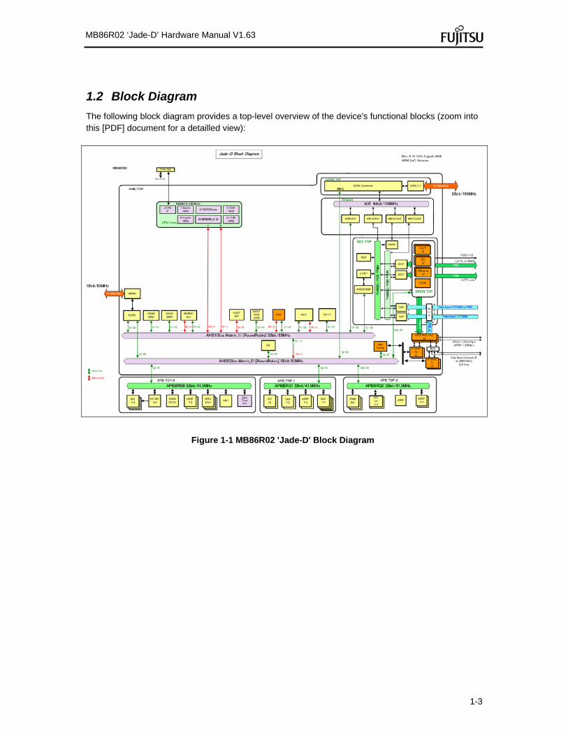
1-3
MB86R02 ‘Jade-D’ Hardware Manual V1.63
1.2 Block Diagram
The following block diagram provides a top-level overview of the device's functional blocks (zoom into this [PDF] document for a detailled view):
Figure 1-1 MB86R02 'Jade-D' Block Diagram
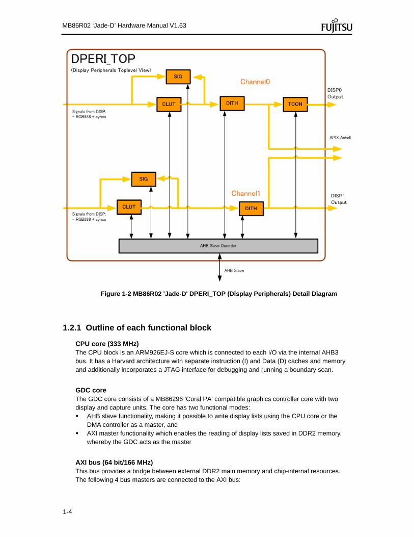
1-4
MB86R02 ‘Jade-D’ Hardware Manual V1.63
Figure 1-2 MB86R02 'Jade-D' DPERI_TOP (Display Peripherals) Detail Diagram
1.2.1 Outline of each functional block
CPU core (333 MHz) The CPU block is an ARM926EJ-S core which is connected to each I/O via the internal AHB3 bus. It has a Harvard architecture with separate instruction (I) and Data (D) caches and memory and additionally incorporates a JTAG interface for debugging and running a boundary scan.
GDC core The GDC core consists of a MB86296 'Coral PA' compatible graphics controller core with two display and capture units. The core has two functional modes: AHB slave functionality, making it possible to write display lists using the CPU core or the
DMA controller as a master, and AXI master functionality which enables the reading of display lists saved in DDR2 memory,
whereby the GDC acts as the master
AXI bus (64 bit/166 MHz) This bus provides a bridge between external DDR2 main memory and chip-internal resources. The following 4 bus masters are connected to the AXI bus:

1-5
MB86R02 ‘Jade-D’ Hardware Manual V1.63
AHB1: Each bus master of the AHB bus (e.g. the CPU core and the DMA controller) AHB3: The connection to the CPU core HBUS: The HOST interface of the GDC DRAW & GEO: DRAW, the drawing engine (2D/3D drawing) and GEO, the geometry
engine of the GDC MBUS: DISP (display controller) and CAP (video capture) of the GDC
AHB1 bus (32 bit/83 MHz) The following resources are connected to the AHB1 bus: GDC: GDC registers AHB2AXI: AXI port for external main memory access CCPB: Encrypted ROM decoding block External BUS I/F: External bus interface (connected through CCPB) SRAM: General purpose internal SRAM 32KB 2 DMAC: General purpose DMA 8ch. This operates as a bus master during data transfer TIC (Test Interface Controller) Boot ROM: Built-in boot ROM (32KB) RLD (Run-Length De-compression unit). Used e.g. for fast logo display MLB: MediaLB controller SDMC: SD memory controller Host SPI (Serial Peripheral Interface) SPI is a serial interface for synchronous
communication APIX Remote Handler (RX/TX channels can act as Master or Slave) AHB2 bus
AHB2 bus (32 bit/83 MHz) CCPB: Encrypted ROM decoding block DDR2 controller: DDR2 controller registers Host SPI (Serial Peripheral Interface) SPI is a serial interface for synchronous
communication I2S_0: Serial audio controller 1ch APBBRG0/1/2: AHB-APB bridge circuit 3ch AHB1 bus
AHB3 bus (32 bit/166 MHz) The following resources are connected to the AHB3 bus:
GDC: GDC registers AHB2AXI: AXI port for external main memory access
AHB2 bus
APB_TOP_0 (32 bit/41.5 MHz) This block acts as a bridge between the AHB2 bus (via the APBBRG0 async module) and the following low-speed peripheral resources: Interrupt controller (IRC) 3ch External interrupt controller (EXTIRC) x 4ch Clock reset generator (CRG) SSCG (Spread-spectrum Clock Generator) for reduced EMI UART (ch0 and ch1) 2ch GPIO x 24ch Remap boot controller (RBC)

1-6
MB86R02 ‘Jade-D’ Hardware Manual V1.63
32 bit general-purpose timer (32 bit timer) 2ch
APB_TOP_1 (32 bit/41.5 MHz) This block acts as a bridge between the AHB2 bus via the APBBRG1 async module and the following low-speed peripheral resources: I2C controller 2ch CAN controller 2ch UART (ch2 and ch3) 2ch A/D converter (ADC) 4ch
APB_TOP_2 (32 bit/41.5 MHz) This block acts as a bridge between the AHB2 bus via the APBBRG2 async module and the following low-speed peripheral resources: PWM controller (PWM) x 8ch SPI controller (SPI) x 2 Chip control module (CCNT) UART (ch4 and ch5) 2ch
Function Summary of the Blocks
Function Outline
CPU core
ARM926EJ-STM processor core
Core operation frequency: 333MHz
16KB instruction cache
16KB data cache
Tightly-Coupled memory for 16KB instruction (ITCM)
Tightly-Coupled memory for 16KB data (DTCM)
ETM9CS Single and JTAG ICE debugging interface
Java acceleration (Jazelle technology)
Bus architecture Multilayer AHB bus architecture
ransfer between main memory and each bus master via 64 bit AXI bus
Interrupts High-speed interrupt 1ch (software interrupt)
Normal interrupt 64ch (external interrupt 4ch + built-in internal interrupt 60ch) terrupt levels are settable by channel
Clock PLL multiplication: selectable
Operation frequency: 333MHz (CPU), 83MHz (AHB1/2), 166MHz (AHB3), 41.5MHz (APB)
Low power consumption mode (clock to ARM and module is stoppable)
Reset Hardware reset, software reset, and watchdog reset
Remap ROM area can be mapped to embedded SRAM area
External bus interface Three chip select signals
Provided 32M byte address space in each chip select
Supported 16/32 bit width SRAM/Flash ROM connection
Programmable weight controller
Encrypted ROM compound engine
DDR2 controller Supported DDR2SDRAM
Connectable capacity: 256 ~ 512M bit 2 or 256 ~ 512M bit 1
I/O width: Selectable from 16/32 bit
Max. transfer rate (32 bit): 166MHz/333Mbps

1-7
MB86R02 ‘Jade-D’ Hardware Manual V1.63
Function Outline
Built-in SRAM Embedded general purpose SRAM 32KB 2 (32 bit bus)
DMAC AHB connection 8ch
Transfer mode: Block, burst, and demand
Timer 32/16 bit programmable 2 channels
GPIO(*2) Max. 24 usable channels
Interrupt function
PWM(*2) 8 channels
Duty ratio and phase are configurable
ADC 10 bit successive approximation type A/D converter 4ch
Sampling rate: 648KS/s (max. sampling plate)
Nonlinearity error: ± 2.0LSB (max.)
GDC (*1) Display controller
RGB666 or RGB888 output
Max. 6 layered display
Max. 2 screen output (RGB)
Digital video capture function
Max. 2 inputs: ITU656 or RGB + ITU656
Geometry engine (MB86296 compatible display list is usable)
2D/3D drawing function (MB86296 compatible display list is usable)
APIX Remote Handler 2ch, Master or Slave functionality
I2S (*2) Audio output/ input 1ch (L/R)
Supported three-wire serial (I2S, MSB-Justified) and serial PCM data transfer interface
Master/Slave operations are selectable
Resolution capability: Max. 32 bit/sample
UART (*2) Max. 6 channels (dedicated channel: 6ch)
1 channel: capable of input/output CTS/RTS signals
8 bit pre-scaler for baud rate clock generation
Enabled DMA transfer
I2C 3.3V pin 2ch
Supported standard mode (max. 100kbps)/high-speed mode (max. 400kbps)
SPI (*2) 2ch
Full duplex/Synchronous transmission
Transfer data length: 1 bit unit (max. 32 bit) (programmable setting)
The length of the SPI interface packets is variable to permit the use of variable length
addresses and data accesses
Supports writes/reads to the internal module connected to the AHB (variable, from 1 to 16
bytes)
Conforms to Freescale Semiconductor's advocacy SPI (CPOL=0, CPHA=0)
Corresponds to the speed of general purpose CPUs (set the frequency of SPICLK to 1/2 or
less of the HCLK frequency)
Host CPU handshaking communication makes software flow control possible
The MB86R02 can only operate in slave mode whereas the host CPU is the bus master
The packet sizes must be in 8 bit units
No CRC error detection functionality.
No automatic procedure for resends in the case of errors (no ARQ functionality)
Supported burst transfer modes for the AHB are single, incr or incr4
Correct operation cannot be guaranteed if simultaneous access to the module occurs from
the APIX-LINK unit
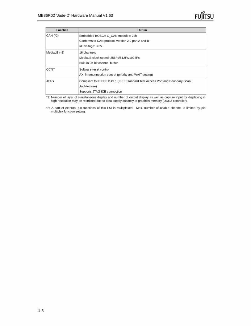
1-8
MB86R02 ‘Jade-D’ Hardware Manual V1.63
Function Outline
CAN (*2) Embedded BOSCH C_CAN module 2ch
Conforms to CAN protocol version 2.0 part A and B
I/O voltage: 3.3V
MediaLB (*2) 16 channels
MediaLB clock speed: 256Fs/512Fs/1024Fs
Built-in 9K bit channel buffer
CCNT Software reset control
AXI interconnection control (priority and WAIT setting)
JTAG Compliant to IEIEEE1149.1 (IEEE Standard Test Access Port and Boundary-Scan
Architecture)
Supports JTAG ICE connection
*1: Number of layer of simultaneous display and number of output display as well as capture input for displaying in high resolution may be restricted due to data supply capacity of graphics memory (DDR2 controller).
*2: A part of external pin functions of this LSI is multiplexed. Max. number of usable channel is limited by pin
multiplex function setting.

1-9
MB86R02 ‘Jade-D’ Hardware Manual V1.63
1.3 Package Dimensions
The package dimensions of the MB86R02 'Jade-D' are shown in the following figure. A separate specification possibly containing more detail may be available on the GDC website: http://www.fujitsu.com/emea/services/microelectronics/gdc/

1-10
MB86R02 ‘Jade-D’ Hardware Manual V1.63
1.4 Pinning
The pin out functionality of the MB86R02 'Jade-D' device is described in this section.
1.5 Pin Assignment
The following figure shows the pin out assignment of the MB86R02 'Jade-D'.
Figure 1-3 Pin Assignment (top view)

1-11
MB86R02 ‘Jade-D’ Hardware Manual V1.63
The following figure shows the pin assignment in functional groups.
APIX related pins
Figure 1-4 Functional Pin Assignment (top view)

1-12
MB86R02 ‘Jade-D’ Hardware Manual V1.63
1.5.1 Pin Assignment Table
JEDEC PIN PKGPinName
A1 1 VSS
B1 2 VSS
C1 3 DE1
D1 4 GV1
E1 5 VSS
F1 6 DOUTB1_4
G1 7 DOUTG1_2
H1 8 DOUTG1_6
J1 9 DOUTR1_4
K1 10 VDDE
L1 11 DISP0P
M1 12 DISP2P
N1 13 DISP4P
P1 14 DISP6P
R1 15 DISP8P
T1 16 DISP10P
U1 17 DCLKP
V1 18 VSS
W1 19 TSG_4
Y1 20 TSG_6
AA1 21 TSG_10
AB1 22 VIN0_4
AC1 23 VIN0_0
AD1 24 CCLK0
AE1 25 VSS
AF1 26 VSS
AF2 27 CCLK1
AF3 28 VIN1_6
AF4 29 VIN1_4
AF5 30 VIN1_0
AF6 31 MLB_DAT
AF7 32 VSS
AF8 33 I2S_ECLK
AF9 34 CAN_RX1
AF10 35 PWM_O3
AF11 36 HOST_SPI_SCK
AF12 37 VPD
AF13 38 AVD1
AF14 39 AVS1
AF15 40 DDRTYPE
AF16 41 UART_SIN0
AF17 42 UART_SIN1
AF18 43 SPI_DI0
AF19 44 SPI_DI1
AF20 45 I2C_SCL1
AF21 46 VDDE

1-13
MB86R02 ‘Jade-D’ Hardware Manual V1.63
AF22 47 INT_A_0
AF23 48 MA_8
AF24 49 MA_12
AF25 50 VSS
AF26 51 VSS
AE26 52 MA_7
AD26 53 MA_3
AC26 54 MA_1
AB26 55 MBA_1
AA26 56 VSS
Y26 57 MDQSN_0
W26 58 MDQSP_0
V26 59 VSS
U26 60 MDQSN_1
T26 61 MDQSP_1
R26 62 VSS
P26 63 MCKN
N26 64 MCKP
M26 65 VSS
L26 66 MDQSN_2
K26 67 MDQSP_2
J26 68 VSS
H26 69 MDQSN_3
G26 70 MDQSP_3
F26 71 VSS
E26 72 MEM_ED_3
D26 73 MEM_ED_7
C26 74 MEM_ED_11
B26 75 VSS
A26 76 VSS
A25 77 VSS
A24 78 MEM_EA_1
A23 79 MEM_EA_4
A22 80 MEM_EA_8
A21 81 MEM_EA_12
A20 82 MEM_EA_16
A19 83 MEM_EA_20
A18 84 VSS
A17 85 MEM_XRD
A16 86 ECLK
A15 87 CRIPM0
A14 88 VCM1
A13 89 SDIN1M
A12 90 APIXVSS
A11 91 XTAL0
A10 92 APIXVSS
A9 93 SDIN0M
A8 94 VCM0
A7 95 OSC_MODE0
A6 96 TRACEDATA_0

1-14
MB86R02 ‘Jade-D’ Hardware Manual V1.63
A5 97 TRACEDATA_1
A4 98 XTRST
A3 99 TDO
A2 100 VSS
B2 101 DCLKIN1
C2 102 DCLKO1
D2 103 HSYNC1
E2 104 DOUTB1_2
F2 105 DOUTB1_5
G2 106 DOUTG1_3
H2 107 DOUTG1_7
J2 108 DOUTR1_5
K2 109 CLK_SEL
L2 110 DISP0N
M2 111 DISP2N
N2 112 DISP4N
P2 113 DISP6N
R2 114 DISP8N
T2 115 DISP10N
U2 116 DCLKN
V2 117 VDDE
W2 118 GV0
Y2 119 TSG_7
AA2 120 TSG_11
AB2 121 VIN0_5
AC2 122 VIN0_1
AD2 123 VINHSYNC0
AE2 124 VDDE
AE3 125 VIN1_7
AE4 126 VIN1_5
AE5 127 VIN1_1
AE6 128 MLB_SIG
AE7 129 MLB_CLK
AE8 130 VDDE
AE9 131 CAN_TX1
AE10 132 PWM_O2
AE11 133 HOST_SPI_DI
AE12 134 TESTMODE_3
AE13 135 AD_VRH0
AE14 136 AD_VRH1
AE15 137 TESTMODE_1
AE16 138 UART_SOUT0
AE17 139 UART_SOUT1
AE18 140 SPI_DO0
AE19 141 SPI_DO1
AE20 142 I2C_SDA1
AE21 143 INT_A_1
AE22 144 MCKE_START
AE23 145 MA_13
AE24 146 MA_4

1-15
MB86R02 ‘Jade-D’ Hardware Manual V1.63
AE25 147 MA_11
AD25 148 MA_5
AC25 149 MA_10
AB25 150 MBA_0
AA25 151 MCKE
Y25 152 MDQ_2
W25 153 MDQ_0
V25 154 VREF0
U25 155 MDQ_13
T25 156 MDQ_8
R25 157 MDQ_15
P25 158 DDRVDE
N25 159 DDRVDE
M25 160 MDQ_21
L25 161 MDQ_16
K25 162 VREF1
J25 163 MDQ_29
H25 164 MDQ_24
G25 165 MDQ_31
F25 166 MEM_ED_0
E25 167 MEM_ED_4
D25 168 MEM_ED_8
C25 169 MEM_ED_12
B25 170 MEM_ED_14
B24 171 MEM_ED_15
B23 172 MEM_EA_3
B22 173 MEM_EA_7
B21 174 MEM_EA_11
B20 175 MEM_EA_15
B19 176 MEM_EA_19
B18 177 MEM_EA_23
B17 178 MEM_XWR_1
B16 179 MEM_XCS_4
B15 180 CRIPM1
B14 181 CRIPM3
B13 182 SDIN1P
B12 183 APIXVD12
B11 184 XTAL1
B10 185 APIXVD12
B9 186 SDIN0P
B8 187 OSC_MODE1
B7 188 RTCK
B6 189 TRACECTL
B5 190 TRACEDATA_2
B4 191 TMS
B3 192 TDI
C3 193 VDDE
D3 194 VSYNC1
E3 195 DOUTB1_3
F3 196 DOUTB1_6

1-16
MB86R02 ‘Jade-D’ Hardware Manual V1.63
G3 197 DOUTG1_4
H3 198 DOUTR1_2
J3 199 DOUTR1_6
K3 200 MPX_MODE_1_1
L3 201 DISP1P
M3 202 DISP3P
N3 203 DISP5P
P3 204 DISP7P
R3 205 DISP9P
T3 206 DISP11P
U3 207 MPX_MODE_5_1
V3 208 VSYNC0
W3 209 HSYNC0
Y3 210 TSG_8
AA3 211 TSG_12
AB3 212 VIN0_6
AC3 213 VIN0_2
AD3 214 VINVSYNC0
AD4 215 VINFID1
AD5 216 VIN1_2
AD6 217 VINVSYNC1
AD7 218 I2S_SDO
AD8 219 I2S_SCK
AD9 220 CAN_RX0
AD10 221 PWM_O1
AD11 222 HOST_SPI_DO
AD12 223 TESTMODE_2
AD13 224 AD_VIN2
AD14 225 AD_VIN3
AD15 226 TESTMODE_0
AD16 227 UART_XCTS0
AD17 228 UART_SIN2
AD18 229 SPI_SS0
AD19 230 SPI_SS1
AD20 231 I2C_SCL0
AD21 232 INT_A_2
AD22 233 IDLLRST
AD23 234 MA_9
AD24 235 MA_6
AC24 236 MA_2
AB24 237 MWE
AA24 238 MRAS
Y24 239 MDQ_5
W24 240 MDQ_1
V24 241 MDQ_7
U24 242 MDQ_10
T24 243 MDQ_9
R24 244 MDM_1
P24 245 VSS
N24 246 VSS

1-17
MB86R02 ‘Jade-D’ Hardware Manual V1.63
M24 247 MDQ_18
L24 248 MDQ_17
K24 249 MDQ_23
J24 250 MDQ_26
H24 251 MDQ_28
G24 252 MDM_3
F24 253 MEM_ED_1
E24 254 MEM_ED_5
D24 255 MEM_ED_9
C24 256 MEM_ED_13
C23 257 MEM_EA_2
C22 258 MEM_EA_6
C21 259 MEM_EA_10
C20 260 MEM_EA_14
C19 261 MEM_EA_18
C18 262 MEM_EA_22
C17 263 MEM_XWR_0
C16 264 MEM_XCS_2
C15 265 CRIPM2
C14 266 SVD
C13 267 APIXVSS
C12 268 OSC_FILTER
C11 269 APIXVD33
C10 270 ATST
C9 271 APIXVSS
C8 272 OSC_BIAS0
C7 273 XSRST
C6 274 TESTMODE_4
C5 275 TRACEDATA_3
C4 276 TCK
D4 277 TRACECLK
E4 278 PLLTDTRST
F4 279 DOUTB1_7
G4 280 DOUTG1_5
H4 281 DOUTR1_3
J4 282 DOUTR1_7
K4 283 MPX_MODE_1_0
L4 284 DISP1N
M4 285 DISP3N
N4 286 DISP5N
P4 287 DISP7N
R4 288 DISP9N
T4 289 DISP11N
U4 290 MPX_MODE_5_0
V4 291 DE0
W4 292 TSG_5
Y4 293 TSG_9
AA4 294 VINFID0
AB4 295 VIN0_7
AC4 296 VIN0_3

1-18
MB86R02 ‘Jade-D’ Hardware Manual V1.63
AC5 297 VIN1_3
AC6 298 VINHSYNC1
AC7 299 I2S_WS
AC8 300 I2S_SDI
AC9 301 CAN_TX0
AC10 302 PWM_O0
AC11 303 HOST_SPI_SS
AC12 304 VSS
AC13 305 AD_VIN0
AC14 306 AD_VIN1
AC15 307 VSS
AC16 308 UART_XRTS0
AC17 309 UART_SOUT2
AC18 310 SPI_SCK0
AC19 311 SPI_SCK1
AC20 312 I2C_SDA0
AC21 313 INT_A_3
AC22 314 ODTCONT
AC23 315 MA_0
AB23 316 MCS
AA23 317 MCAS
Y23 318 MDQ_3
W23 319 MDQ_4
V23 320 MDM_0
U23 321 MDQ_11
T23 322 MDQ_12
R23 323 MDQ_14
P23 324 OCD
N23 325 ODT
M23 326 MDQ_19
L23 327 MDQ_20
K23 328 MDM_2
J23 329 MDQ_27
H23 330 MDQ_25
G23 331 MDQ_30
F23 332 MEM_ED_2
E23 333 MEM_ED_6
D23 334 MEM_ED_10
D22 335 MEM_EA_5
D21 336 MEM_EA_9
D20 337 MEM_EA_13
D19 338 MEM_EA_17
D18 339 MEM_EA_21
D17 340 MEM_EA_24
D16 341 MEM_XCS_0
D15 342 MEM_RDY
D14 343 SVS
D13 344 SDOUT1M
D12 345 APIXVD12
D11 346 RREF

1-19
MB86R02 ‘Jade-D’ Hardware Manual V1.63
D10 347 APIXVD12
D9 348 SDOUT0M
D8 349 OSC_BIAS1
D7 350 VSS
D6 351 XRST
D5 352 VINITHI
E5 353 VDDE
F5 354 VDDE
G5 355 VDD
H5 356 VDD
J5 357 VSS
K5 358 VSS
L5 359 VDDE
M5 360 VDDE
N5 361 VDD
P5 362 VDD
R5 363 VSS
T5 364 VSS
U5 365 VDDE
V5 366 VDDE
W5 367 VDD
Y5 368 VDD
AA5 369 VSS
AB5 370 VSS
AB6 371 VDDE
AB7 372 VDDE
AB8 373 VDD
AB9 374 VDD
AB10 375 VDDE
AB11 376 VSS
AB12 377 AD_VRL0
AB13 378 AD_VR0
AB14 379 AD_VR1
AB15 380 AD_VRL1
AB16 381 VSS
AB17 382 VSS
AB18 383 VDDE
AB19 384 VDDE
AB20 385 VDD
AB21 386 VDD
AB22 387 DDRVDE
AA22 388 DDRVDE
Y22 389 VSS
W22 390 VSS
V22 391 MDQ_6
U22 392 DDRVDE
T22 393 DDRVDE
R22 394 VSS
P22 395 VDD
N22 396 VDD
1-20
MB86R02 ‘Jade-D’ Hardware Manual V1.63
M22 397 VSS
L22 398 MDQ_22
K22 399 DDRVDE
J22 400 DDRVDE
H22 401 VSS
G22 402 VSS
F22 403 VDD
E22 404 VDD
E21 405 VDDE
E20 406 VDDE
E19 407 VSS
E18 408 VDDE
E17 409 VDD
E16 410 VDD
E15 411 VSS
E14 412 PVD
E13 413 PVS
E12 414 SDOUT1P
E11 415 APIXVSS
E10 416 APIXVSS
E9 417 SDOUT0P
E8 418 JTAGSEL
E7 419 VSS
E6 420 VSS
K10 421 VDD
L10 422 VDD
M10 423 VDDE
N10 424 VDDE
P10 425 VDD
R10 426 VDD
T10 427 VDDE
U10 428 VDDE
U11 429 VDD
U12 430 VDD
U13 431 VDDE
U14 432 VDDE
U15 433 VDD
U16 434 VDD
U17 435 DDRVDE
T17 436 DDRVDE
R17 437 VDD
P17 438 VDD
N17 439 DDRVDE
M17 440 DDRVDE
L17 441 VDD
K17 442 VDD
K16 443 VDDE
K15 444 VDDE
K14 445 VDD
K13 446 VDD

1-21
MB86R02 ‘Jade-D’ Hardware Manual V1.63
K12 447 VDDE
K11 448 VDDE
L11 449 VSS
M11 450 VSS
N11 451 VSS
P11 452 VSS
R11 453 VSS
T11 454 VSS
T12 455 VSS
T13 456 VSS
T14 457 VSS
T15 458 VSS
T16 459 VSS
R16 460 VSS
P16 461 VSS
N16 462 VSS
M16 463 VSS
L16 464 VSS
L15 465 VSS
L14 466 VSS
L13 467 VSS
L12 468 VSS
M12 469 VSS
N12 470 VSS
P12 471 VSS
R12 472 VSS
R13 473 VSS
R14 474 VSS
R15 475 VSS
P15 476 VSS
N15 477 VSS
M15 478 VSS
M14 479 VSS
M13 480 VSS
N13 481 VSS
P13 482 VSS
P14 483 VSS
N14 484 VSS

1-22
MB86R02 ‘Jade-D’ Hardware Manual V1.63
1.5.2 Pin Multiplexing
In order to maintain a smaller pin count despite full hardware functionality, MB86R02 'Jade-D' uses pin multiplexing. This means that in a specific pin multiplex mode, certain package pins are internally rerouted (shared between different units) so that their external functionality is changed. Package pins are categorized into different modes (tables), which are configured using various pin multiplex functions. Pin Multiplex Overview Pin multiplex mode #0 Dependancies: setting of register MPX_MODE_1[1:0]
• First MUX Function: Pins related to Display1 • Second MUX Function: Pins related to external bus 32 bit interface • Third MUX Function: Pins related to Display1
Pin multiplex mode #1 Dependancies: setting of register: MPX_MODE_1[1:0]
• First MUX Function: Pins related to Capture0, Capture1 • Second MUX Function: Pins related to Capture0, Capture1 • Third MUX Function: Pins related to external bus 32 bit interface
Pin multiplex mode #2 Dependancies: setting of registers: CMPX_MODE_9[1:0] and
CMPX_MODE_2[1:0] and MPX_MODE_5[1]
• First MUX Function: Pins related to UART0 • Second MUX Function: Pins related to GPIO • Third MUX Function: Pins related to UART0, UART3 • Fourth MUX Function: Pins related to Memory NAND flash
Pin multiplex mode #3 Dependancies: setting of register: MPX_MODE_5[0]
• First MUX Function: Pins related to JTAG Tracing • Second MUX Function: Pins related to PWM
Pin multiplex mode #4 Dependancies: setting of register: CMPX_MODE_2[1:0]
• First MUX Function: Pins related to DISP0 • Second MUX Function: Pins related to DISP0, APIX SB0 • Third MUX Function: Pins related to APIX SB0, GPIOx18 • Fourth MUX Function: Pins related to GPIOx24

1-23
MB86R02 ‘Jade-D’ Hardware Manual V1.63
Pin multiplex mode #5 Dependancies: setting of registers: CMPX_MODE_3[1:0] and
CMPX_MODE_2[1:0]
• First MUX Function: Pins related to TCON • Second MUX Function: Pins related to GPIO • Third MUX Function: Pins related to APIX SB
Pin multiplex mode #6 Dependancies: setting of register: CMPX_MODE_6[0]
• First MUX Function: Pins related to I2S • Second MUX Function: Pins related to PWM4,5,6,7
Pin multiplex mode #7 Dependancies: setting of register: CMPX_MODE_7[0]
• First MUX Function: Pins related to PWM0,1,2,3 • Second MUX Function: Pins related to UART4,5
Pin multiplex mode #8 Dependancies: setting of registers: CMPX_MODE_8[0] and
CMPX_MODE_2[1:0] • First MUX Function: Pins related to SPI Host • Second MUX Function: Pins related to GPIO8,9,10,11
Pin multiplex mode #9: Does not exist! Pin multiplex mode #10 Dependancies: setting of registers: CMPX_MODE_10[1:0] and
CMPX_MODE_2[1:0]
• First MUX Function: Pins related to UART0 • Second MUX Function: Pins related to GPIO16 … 19. • Third MUX Function: Pins related to SD
Pin multiplex mode #11 Dependancies: setting of registers: CMPX_MODE_11[0] and
CMPX_MODE_2[1:0]
• First MUX Function: Pins related to SPI • Second MUX Function: Pins related to GPIO20 ... 23

1-24
MB86R02 ‘Jade-D’ Hardware Manual V1.63
Note: You should only change the pin multiplex mode when none of the pins effected by the mode switch are in use.
Fixed after bootup (configured via hardware, mode pins)
Function fixed after bootup (capture), but ITU/RGB function is still configurable by register
CMPX_MODE_4[0] (MPXTABLE5)
Function fixed after bootup (UART0), but other functions still configurable by register CMPX_MODE_9[1:0],
CMPX_MODE_2[1:0] (MPX_TABLE9)
Configurable by register (software action)
ES1/
ES2 Modification/extension ES1-->ES2
CONST0 = Drives '0' constantly to this pin. Note: The first column of each of the following tables is the default state! If a non-specified mode is selected then the default mode is applied (e.g. MUX Mode #0, '11' > first MUX function applies).

1-25
MB86R02 ‘Jade-D’ Hardware Manual V1.63
Pin multiplex mode #0 First MUX Function Second MUX Function Third MUX Function
MPX_MODE_1[1:0] = > "00" "01" "10"
Functional Group -> DISP1 MEMC 32bit Ext. DISP1
Pin Name: 1st Function: 2nd Function: 3rd Function:
DE1 DE1 XDACK_7 DE1
GV1 GV1 DREQ_7 GV1
HSYNC1 HSYNC1 DREQ_6 HSYNC1
VSYNC1 VSYNC1 XDACK_6 VSYNC1
DOUTB1_2 DOUTB1_2 MEM_XWR_2 DOUTB1_2
DOUTB1_3 DOUTB1_3 MEM_XWR_3 DOUTB1_3
DOUTB1_4 DOUTB1_4 MEM_ED_16 DOUTB1_4
DOUTB1_5 DOUTB1_5 MEM_ED_17 DOUTB1_5
DOUTB1_6 DOUTB1_6 MEM_ED_18 DOUTB1_6
DOUTB1_7 DOUTB1_7 MEM_ED_19 DOUTB1_7
DOUTG1_2 DOUTG1_2 MEM_ED_20 DOUTG1_2
DOUTG1_3 DOUTG1_3 MEM_ED_21 DOUTG1_3
DOUTG1_4 DOUTG1_4 MEM_ED_22 DOUTG1_4
DOUTG1_5 DOUTG1_5 MEM_ED_23 DOUTG1_5
DOUTG1_6 DOUTG1_6 MEM_ED_24 DOUTG1_6
DOUTG1_7 DOUTG1_7 MEM_ED_25 DOUTG1_7
DOUTR1_2 DOUTR1_2 MEM_ED_26 DOUTR1_2
DOUTR1_3 DOUTR1_3 MEM_ED_27 DOUTR1_3
DOUTR1_4 DOUTR1_4 MEM_ED_28 DOUTR1_4
DOUTR1_5 DOUTR1_5 MEM_ED_29 DOUTR1_5
DOUTR1_6 DOUTR1_6 MEM_ED_30 DOUTR1_6
DOUTR1_7 DOUTR1_7 MEM_ED_31 DOUTR1_7

1-26
MB86R02 ‘Jade-D’ Hardware Manual V1.63
Pin multiplex mode #1 First MUX Function Second MUX Function Third MUX Function
MPX_MODE_1[1:0] = > "00" "01" "10"
Functional Group -> CAP0,1 ITU CAP0,1 RGB MEMC 32bit Ext.
Pin Name: 1st Function: 2nd Function: 3rd Function:
VINFID0 VINFID0 GI1_3 MEM_ED_31
VIN0_4 VIN0_4 RI1_4 MEM_ED_30
VIN0_5 VIN0_5 RI1_5 MEM_ED_29
VIN0_6 VIN0_6 RI1_6 MEM_ED_28
VIN0_7 VIN0_7 RI1_7 MEM_ED_27
VIN0_0 VIN0_0 GI1_6 MEM_ED_26
VIN0_1 GI1_7 MEM_ED_25
VIN0_2 RI1_2 MEM_ED_24
VIN0_3 RI1_3 MEM_ED_23
CCLK0 CCLK0 CCLK0
VINHSYNC0 GI1_4 MEM_ED_22
VINVSYNC0 GI1_5 MEM_ED_21
CCLK1 CCLK1 CCLK1
VIN1_6 BI1_7 MEM_ED_20
VIN1_7 GI1_2 MEM_ED_19
VIN1_4 BI1_5 MEM_ED_18
VIN1_5 BI1_6 MEM_ED_17
VINFID1 VINFID1 MEM_ED_16
VIN1_0 CONST0 MEM_XWR_3
VIN1_1 BI1_2 MEM_XWR_2
VIN1_2 BI1_3 DREQ_7
VIN1_3 BI1_4 XDACK_7
VINVSYNC1 VINVSYNC1 XDACK_6
VINHSYNC1 VINHSYNC1 DREQ_6
Pin multiplex mode #2 First MUX
Function
Second MUX
Function
Third MUX
Function Fourth MUX Function
CMPX_MODE_9[1:0],
CMPX_MODE_2[1:0],
MPX_MODE_5[1]
"00",
"XX",
"0"
"01",
"0X",
"0"
"10",
"XX",
"0"
"XX",
"XX",
"1"
Functional Group -> UART0 GPIO[15:12] UART0, UART3 MEMC NAND Flash
Pin Name: 1st Function: 2nd Function: 3rdFunction: 4th Function:
UART_SIN0 UART_SIN0 GPIO_PD_12 UART_SIN0 MNREX
UART_SOUT0 UART_SOUT0 GPIO_PD_13 UART_SOUT0 MNWEX
UART_XCTS0 UART_XCTS0 GPIO_PD_14 UART_SIN3 MNCLE
UART_XRTS0 UART_XRTS0 GPIO_PD_15 UART_SOUT3 MNALE

1-27
MB86R02 ‘Jade-D’ Hardware Manual V1.63
Pin multiplex mode #3 First MUX Function Second MUX Function
MPX_MODE_5[0] "0" "1"
Functional Group -> TRACE PWM
Pin Name: 1st Function: 2nd Function:*
TRACEDATA_0 TRACEDATA_0 PWM_07
TRACEDATA_1 TRACEDATA_1 PWM_04
TRACEDATA_2 TRACEDATA_2 PWM_05
TRACEDATA_3 TRACEDATA_3 PWM_06
* Please note that in this mode, if the pins (C5, B5, A5, A6) are unused in multiplex mode #3, then an external termination is
not required because the pins are in output mode. To make sure that the pins do not oscillate, check PWMxSR[0] = 0 (i.e. Stop
PWM) is set.
Pin multiplex mode #4 First MUX
Function
Second MUX
Function Third MUX Function Fourth MUX Function
CMPX_MODE_2[1:0] "00" */** "01" "10" "11"
Functional Group -> DISP0 DISP0 & APIX0_SB APIX0_SB & GPIOx18 GPIOx24
Pin Name: 1st Function: 2nd Function: 3rd Function: Pin Name:
DISP0P DISP0P APIX0_SB_0 APIX0_SB_0 GPIO_PD_0
DISP0N DISP0N APIX0_SB_1 APIX0_SB_1 GPIO_PD_1
DISP1P DISP1P DISP1P GPIO_PD_2 GPIO_PD_2
DISP1N DISP1N DISP1N GPIO_PD_3 GPIO_PD_3
DISP2P DISP2P GPIO_PD_4 GPIO_PD_4
DISP2N DISP2N GPIO_PD_5 GPIO_PD_5
DISP3P DISP3P GPIO_PD_6 GPIO_PD_6
DISP3N DISP3N GPIO_PD_7 GPIO_PD_7
DISP4P APIX0_SB_2 APIX0_SB_2 GPIO_PD_8
DISP4N APIX0_SB_3 APIX0_SB_3 GPIO_PD_9
DISP5P DISP5P GPIO_PD_10 GPIO_PD_10
DISP5N DISP5N GPIO_PD_11 GPIO_PD_11
DISP6P DISP6P GPIO_PD_12 GPIO_PD_12
DISP6N DISP6N GPIO_PD_13 GPIO_PD_13
DISP7P DISP7P GPIO_PD_14 GPIO_PD_14
DISP7N DISP7N GPIO_PD_15 GPIO_PD_15
DISP8P APIX0_SB_4 APIX0_SB_4 GPIO_PD_16
DISP8N APIX0_SB_5 APIX0_SB_5 GPIO_PD_17
DISP9P DISP9P GPIO_PD_18 GPIO_PD_18
DISP9N DISP9N GPIO_PD_19 GPIO_PD_19
DISP10P DISP10P GPIO_PD_20 GPIO_PD_20
DISP10N DISP10N GPIO_PD_21 GPIO_PD_21
DISP11P DISP11P GPIO_PD_22 GPIO_PD_22
DISP11N DISP11N GPIO_PD_23 GPIO_PD_23
DCLKP DCLKP
ES1: Input (no function)
ES2: CONST0
ES1: Input (no function)
ES2: CONST0
DCLKN DCLKN
ES1: Input (no function)
ES2: CONST0
ES1: Input (no function)
ES2: CONST0
VSYNC0 VSYNC0 VSYNC0 VSYNC0
DE0 DE0 DE0 DE0
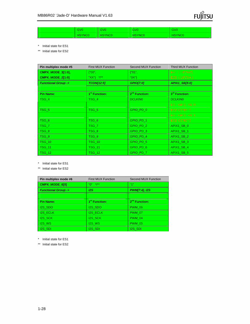
1-28
MB86R02 ‘Jade-D’ Hardware Manual V1.63
GV0 GV0 GV0 GV0
HSYNC0 HSYNC0 HSYNC0 HSYNC0
* Initial state for ES1
** Initial state for ES2
Pin multiplex mode #5 First MUX Function Second MUX Function Third MUX Function
CMPX_MODE_3[1:0],
CMPX_MODE_2[1:0]
"00",
"XX" */**
"01",
"0X"
ES1: "10","0X"
ES2: "10","XX"
Functional Group -> TCON[12:5] GPIO[7:0] APIX1_SB[5:0]
Pin Name: 1st Function: 2nd Function: 3rd Function:
TSG_4 TSG_4 DCLKIN0 DCLKIN0
TSG_5 TSG_5 GPIO_PD_0
ES1: GPIO_PD_0
ES2: CONST0
TSG_6 TSG_6 GPIO_PD_1
ES1: GPIO_PD_1
ES2: CONST0
TSG_7 TSG_7 GPIO_PD_2 APIX1_SB_0
TSG_8 TSG_8 GPIO_PD_3 APIX1_SB_1
TSG_9 TSG_9 GPIO_PD_4 APIX1_SB_2
TSG_10 TSG_10 GPIO_PD_5 APIX1_SB_3
TSG_11 TSG_11 GPIO_PD_6 APIX1_SB_4
TSG_12 TSG_12 GPIO_PD_7 APIX1_SB_5
* Initial state for ES1
** Initial state for ES2
Pin multiplex mode #6 First MUX Function Second MUX Function
CMPX_MODE_6[0] "0" */** "1"
Functional Group -> I2S PWM[7:4], I2S
Pin Name: 1st Function: 2nd Function:
I2S_SDO I2S_SDO PWM_06
I2S_ECLK I2S_ECLK PWM_07
I2S_SCK I2S_SCK PWM_04
I2S_WS I2S_WS PWM_05
I2S_SDI I2S_SDI I2S_SDI
* Initial state for ES1
** Initial state for ES2

1-29
MB86R02 ‘Jade-D’ Hardware Manual V1.63
Pin multiplex mode #7 First MUX Function Second MUX Function
CMPX_MODE_7[0] "0" * "1" **
Functional Group -> PWM[3:0] UART4,5
Pin Name: 1st Function: 2nd Function:
PWM_O3 PWM_O3 UART_SOUT5
PWM_O2 PWM_O2 UART_SIN5
PWM_O1 PWM_O1 UART_SOUT4
PWM_O0 PWM_O0 UART_SIN4
* Initial state for ES1
** Initial state for ES2
Pin multiplex mode #8 First MUX Function Second MUX Function
CMPX_MODE_8[0],
CMPX_MODE_2[1:0]
"0",
"XX" */**
"1",
"0X"
Functional Group -> SPI_HOST GPIO[11:8]
Pin Name: 1st Function: 2nd Function:
HOST_SPI_SCK HOST_SPI_SCK GPIO_PD_8
HOST_SPI_DI HOST_SPI_DI GPIO_PD_9
HOST_SPI_DO HOST_SPI_DO GPIO_PD_10
HOST_SPI_SS HOST_SPI_SS GPIO_PD_11
* Initial state for ES1
** Initial state for ES2
Pin multiplex mode #10 First MUX Function Second MUX Function Third MUX Function
CMPX_MODE_10[1:0],
CMPX_MODE_2[1:0]
"00",
"XX" *
"01",
"0X"
"10",
"XX" **
Functional Group -> UART1,2 SPI(m)1 GPIO[19:16], SPI(m)1 SD
Pin Name: 1st Function: 2nd Function: 3rd Function:
UART_SIN1 UART_SIN1 GPIO_PD_16 SD_DAT_0
UART_SOUT1 UART_SOUT1 GPIO_PD_17 SD_DAT_1
UART_SIN2 UART_SIN2 GPIO_PD_18 SD_DAT_2
UART_SOUT2 UART_SOUT2 GPIO_PD_19 SD_DAT_3
SPI_DI1 SPI_DI1 SPI_DI1 SD_WP
SPI_DO1 SPI_DO1 SPI_DO1 SD_XMCD
SPI_SS1 SPI_SS1 SPI_SS1 SD_CMD
SPI_SCK1 SPI_SCK1 SPI_SCK1 SD_CLK
* Initial state for ES1
** Initial state for ES2

1-30
MB86R02 ‘Jade-D’ Hardware Manual V1.63
Pin multiplex mode #11 First MUX Function Second MUX Function
CMPX_MODE_11[0],
CMPX_MODE_2[1:0]
"0",
"XX" *
"1",
"0X" **
Functional Group -> SPI(m)0 GPIO[23:20]
Pin Name: 1st Function: 2nd Function:
SPI_DI0 SPI_DI0 GPIO_PD_20
SPI_DO0 SPI_DO0 GPIO_PD_21
SPI_SS0 SPI_SS0 GPIO_PD_22
SPI_SCK0 SPI_SCK0 GPIO_PD_23
* Initial state for ES1
** Initial state for ES2
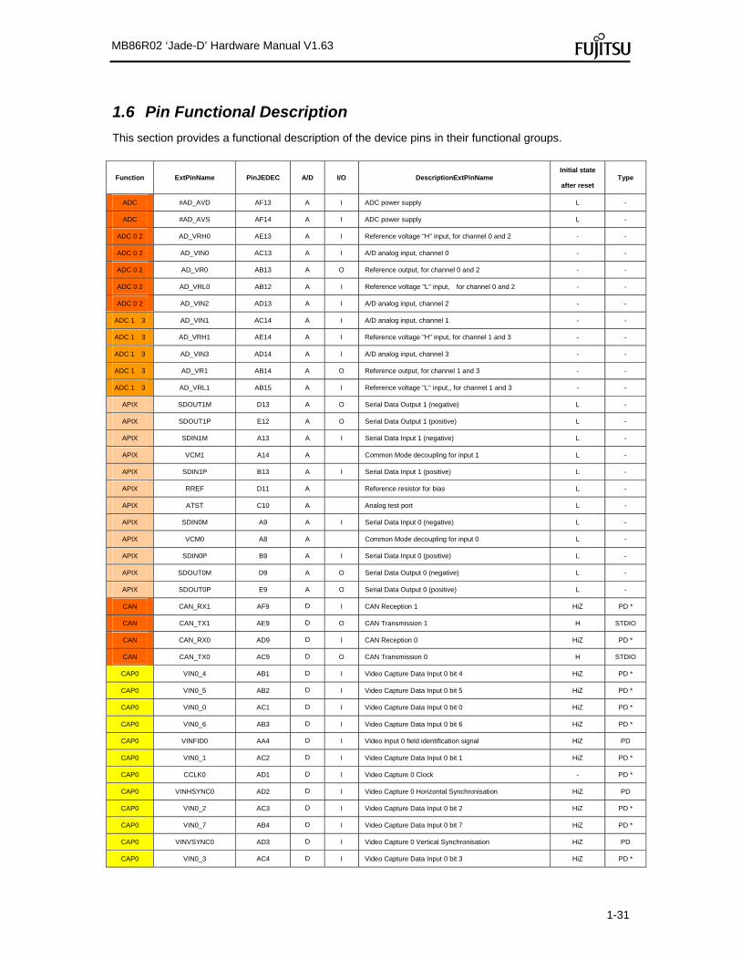
1-31
MB86R02 ‘Jade-D’ Hardware Manual V1.63
1.6 Pin Functional Description
This section provides a functional description of the device pins in their functional groups.
Function ExtPinName PinJEDEC A/D I/O DescriptionExtPinName Initial state
after reset Type
ADC #AD_AVD AF13 A I ADC power supply L -
ADC #AD_AVS AF14 A I ADC power supply L -
ADC 0 2 AD_VRH0 AE13 A I Reference voltage "H" input, for channel 0 and 2 - -
ADC 0 2 AD_VIN0 AC13 A I A/D analog input, channel 0 - -
ADC 0 2 AD_VR0 AB13 A O Reference output, for channel 0 and 2 - -
ADC 0 2 AD_VRL0 AB12 A I Reference voltage "L" input, for channel 0 and 2 - -
ADC 0 2 AD_VIN2 AD13 A I A/D analog input, channel 2 - -
ADC 1 3 AD_VIN1 AC14 A I A/D analog input, channel 1 - -
ADC 1 3 AD_VRH1 AE14 A I Reference voltage "H" input, for channel 1 and 3 - -
ADC 1 3 AD_VIN3 AD14 A I A/D analog input, channel 3 - -
ADC 1 3 AD_VR1 AB14 A O Reference output, for channel 1 and 3 - -
ADC 1 3 AD_VRL1 AB15 A I Reference voltage "L" input,, for channel 1 and 3 - -
APIX SDOUT1M D13 A O Serial Data Output 1 (negative) L -
APIX SDOUT1P E12 A O Serial Data Output 1 (positive) L -
APIX SDIN1M A13 A I Serial Data Input 1 (negative) L -
APIX VCM1 A14 A Common Mode decoupling for input 1 L -
APIX SDIN1P B13 A I Serial Data Input 1 (positive) L -
APIX RREF D11 A Reference resistor for bias L -
APIX ATST C10 A Analog test port L -
APIX SDIN0M A9 A I Serial Data Input 0 (negative) L -
APIX VCM0 A8 A Common Mode decoupling for input 0 L -
APIX SDIN0P B9 A I Serial Data Input 0 (positive) L -
APIX SDOUT0M D9 A O Serial Data Output 0 (negative) L -
APIX SDOUT0P E9 A O Serial Data Output 0 (positive) L -
CAN CAN_RX1 AF9 D I CAN Reception 1 HiZ PD *
CAN CAN_TX1 AE9 D O CAN Transmission 1 H STDIO
CAN CAN_RX0 AD9 D I CAN Reception 0 HiZ PD *
CAN CAN_TX0 AC9 D O CAN Transmission 0 H STDIO
CAP0 VIN0_4 AB1 D I Video Capture Data Input 0 bit 4 HiZ PD *
CAP0 VIN0_5 AB2 D I Video Capture Data Input 0 bit 5 HiZ PD *
CAP0 VIN0_0 AC1 D I Video Capture Data Input 0 bit 0 HiZ PD *
CAP0 VIN0_6 AB3 D I Video Capture Data Input 0 bit 6 HiZ PD *
CAP0 VINFID0 AA4 D I Video input 0 field identification signal HiZ PD
CAP0 VIN0_1 AC2 D I Video Capture Data Input 0 bit 1 HiZ PD *
CAP0 CCLK0 AD1 D I Video Capture 0 Clock - PD *
CAP0 VINHSYNC0 AD2 D I Video Capture 0 Horizontal Synchronisation HiZ PD
CAP0 VIN0_2 AC3 D I Video Capture Data Input 0 bit 2 HiZ PD *
CAP0 VIN0_7 AB4 D I Video Capture Data Input 0 bit 7 HiZ PD *
CAP0 VINVSYNC0 AD3 D I Video Capture 0 Vertical Synchronisation HiZ PD
CAP0 VIN0_3 AC4 D I Video Capture Data Input 0 bit 3 HiZ PD *
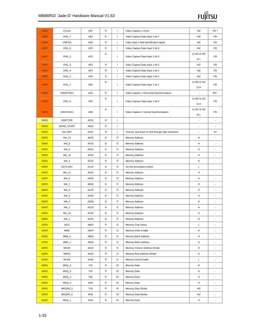
1-32
MB86R02 ‘Jade-D’ Hardware Manual V1.63
CAP1 CCLK1 AF2 D I Video Capture 1 Clock HiZ PD *
CAP1 VIN1_7 AE3 D I Video Capture Data Input 1 bit 7 HiZ PD
CAP1 VINFID1 AD4 D I Video input 1 field identification signal HiZ PD
CAP1 VIN1_6 AF3 D I Video Capture Data Input 1 bit 6 HiZ PD
CAP1 VIN1_3 AC5 D
I Video Capture Data Input 1 bit 3 1) HiZ 2) HiZ
3) L PD
CAP1 VIN1_5 AE4 D I Video Capture Data Input 1 bit 5 HiZ PD
CAP1 VIN1_4 AF4 D I Video Capture Data Input 1 bit 4 HiZ PD
CAP1 VIN1_2 AD5 D I Video Capture Data Input 1 bit 2 HiZ PD
CAP1 VIN1_1 AE5 D
I Video Capture Data Input 1 bit 1 1) HiZ 2) HiZ
3) H PD
CAP1 VINHSYNC1 AC6 D I Video Capture 1 Horizontal Synchronisation - PD *
CAP1 VIN1_0 AF5 D
I Video Capture Data Input 1 bit 0 1) HiZ 2) HiZ
3) H PD
CAP1 VINVSYNC1 AD6 D
I Video Capture 1 Vertical Synchronisation 1) HiZ 2) HiZ
3) L PD
DDR2 DDRTYPE AF15 D I - -
DDR2 MCKE_START AE22 D I - -
DDR2 IDLLRST AD22 D I Test pin, pull down to VSS through high resistance - ST
DDR2 MA_13 AE23 D O Memory Address H -
DDR2 MA_8 AF23 D O Memory Address H -
DDR2 MA_9 AD23 D O Memory Address H -
DDR2 MA_12 AF24 D O Memory Address H -
DDR2 MA_4 AE24 D O Memory Address H -
DDR2 ODTCONT AC22 D O On-Die termination control L
DDR2 MA_11 AE25 D O Memory Address H -
DDR2 MA_6 AD24 D O Memory Address H -
DDR2 MA_7 AE26 D O Memory Address H -
DDR2 MA_0 AC23 D O Memory Address H -
DDR2 MA_5 AD25 D O Memory Address H -
DDR2 MA_3 AD26 D O Memory Address H -
DDR2 MA_2 AC24 D O Memory Address H -
DDR2 MA_10 AC25 D O Memory Address H -
DDR2 MA_1 AC26 D O Memory Address H -
DDR2 MCS AB23 D O Memory Chip Select L -
DDR2 MWE AB24 D O Memory Write Enable H -
DDR2 MBA_0 AB25 D O Memory Bank Address H -
DDR2 MBA_1 AB26 D O Memory Bank Address H -
DDR2 MCAS AA23 D O Memory Column Address Strobe H -
DDR2 MRAS AA24 D O Memory Row Address Strobe H -
DDR2 MCKE AA25 D O Memory Clock Enable L -
DDR2 MDQ_3 Y23 D IO Memory Data H -
DDR2 MDQ_5 Y24 D IO Memory Data H -
DDR2 MDQ_2 Y25 D IO Memory Data H -
DDR2 MDQ_4 W23 D IO Memory Data H -
DDR2 MDQSN_0 Y26 D IO Memory Data Strobe HiZ -
DDR2 MDQSP_0 W26 D IO Memory Data Strobe HiZ -
DDR2 MDQ_1 W24 D IO Memory Data H -

1-33
MB86R02 ‘Jade-D’ Hardware Manual V1.63
DDR2 MDQ_0 W25 D IO Memory Data H -
DDR2 MDQ_6 V22 D IO Memory Data H -
DDR2 MDM_0 V23 D O Memory Data Mask HiZ -
DDR2 MDQ_7 V24 D IO Memory Data H -
DDR2 VREF0 V25 A I Reference Voltage Input - -
DDR2 MDQ_11 U23 D IO Memory Data H -
DDR2 MDQ_10 U24 D IO Memory Data H -
DDR2 MDQ_13 U25 D IO Memory Data H -
DDR2 MDQ_12 T23 D IO Memory Data H -
DDR2 MDQSN_1 U26 D IO Memory Data Strobe HiZ -
DDR2 MDQSP_1 T26 D IO Memory Data Strobe HiZ -
DDR2 MDQ_9 T24 D IO Memory Data H -
DDR2 MDQ_8 T25 D IO Memory Data H -
DDR2 MDQ_14 R23 D IO Memory Data H -
DDR2 MDM_1 R24 D O Memory Data Mask HiZ -
DDR2 MDQ_15 R25 D IO Memory Data H -
DDR2 MCKN P26 D O Memory Clock Output H CLK
DDR2 MCKP N26 D O Memory Clock Output L CLK
DDR2 OCD P23 I A Off-chip driver ref. voltage - -
DDR2 ODT N23 I A On-die termination ref. voltage - -
DDR2 MDQ_19 M23 D IO Memory Data H -
DDR2 MDQ_18 M24 D IO Memory Data H -
DDR2 MDQ_21 M25 D IO Memory Data H -
DDR2 MDQ_20 L23 D IO Memory Data H -
DDR2 MDQSN_2 L26 D IO Memory Data Strobe HiZ -
DDR2 MDQSP_2 K26 D IO Memory Data Strobe HiZ -
DDR2 MDQ_17 L24 D IO Memory Data H -
DDR2 MDQ_16 L25 D IO Memory Data H -
DDR2 MDQ_22 L22 D IO Memory Data H -
DDR2 MDM_2 K23 D O Memory Data Mask HiZ -
DDR2 MDQ_23 K24 D IO Memory Data H -
DDR2 VREF1 K25 A I Reference Voltage Input - -
DDR2 MDQ_27 J23 D IO Memory Data H -
DDR2 MDQ_26 J24 D IO Memory Data H -
DDR2 MDQ_29 J25 D IO Memory Data H -
DDR2 MDQ_25 H23 D IO Memory Data H -
DDR2 MDQSN_3 H26 D IO Memory Data Strobe HiZ -
DDR2 MDQSP_3 G26 D IO Memory Data Strobe HiZ -
DDR2 MDQ_28 H24 D IO Memory Data H -
DDR2 MDQ_24 H25 D IO Memory Data H -
DDR2 MDQ_30 G23 D IO Memory Data H -
DDR2 MDM_3 G24 D O Memory Data Mask HiZ -
DDR2 MDQ_31 G25 D IO Memory Data H -
DISP0 DISP0P L1 D
IO Display 0 output channel 0p, Default=DOUTR0_0 (TTL-
mode) HiZ MSIO
DISP0 DISP0N L2 D
IO Display 0 output channel 0n, Default=DOUTR0_1 (TTL-
mode) HiZ MSIO

1-34
MB86R02 ‘Jade-D’ Hardware Manual V1.63
DISP0 DISP1P L3 D
IO Display 0 output channel 1p, Default=DOUTR0_2 (TTL-
mode) HiZ MSIO
DISP0 DISP1N L4 D
IO Display 0 output channel 1n, Default=DOUTR0_3 (TTL-
mode) HiZ
MSIO
DISP0 DISP2P M1 D
IO Display 0 output channel 2p, Default=DOUTR0_4 (TTL-
mode) HiZ
MSIO
DISP0 DISP2N M2 D
IO Display 0 output channel 2n, Default=DOUTR0_5 (TTL-
mode) HiZ
MSIO
DISP0 DISP3P M3 D
IO Display 0 output channel 3p, Default=DOUTR0_6 (TTL-
mode) HiZ
MSIO
DISP0 DISP3N M4 D
IO Display 0 output channel 3n, Default=DOUTR0_7 (TTL-
mode) HiZ
MSIO
DISP0 DISP4P N1 D
IO Display 0 output channel 4p, Default=DOUTG0_0 (TTL-
mode) HiZ
MSIO
DISP0 DISP4N N2 D
IO Display 0 output channel 4n, Default=DOUTG0_1 (TTL-
mode) HiZ
MSIO
DISP0 DISP5P N3 D
IO Display 0 output channel 5p, Default=DOUTG0_2 (TTL-
mode) HiZ
MSIO
DISP0 DISP5N N4 D
IO Display 0 output channel 5n, Default=DOUTG0_3 (TTL-
mode) HiZ
MSIO
DISP0 DISP6P P1 D
IO Display 0 output channel 6p, Default=DOUTG0_4 (TTL-
mode) HiZ
MSIO
DISP0 DISP6N P2 D
IO Display 0 output channel 6n, Default=DOUTG0_5 (TTL-
mode) HiZ
MSIO
DISP0 DISP7P P3 D
IO Display 0 output channel 7p, Default=DOUTG0_6 (TTL-
mode) HiZ
MSIO
DISP0 DISP7N P4 D
IO Display 0 output channel 7n, Default=DOUTG0_7 (TTL-
mode) HiZ
MSIO
DISP0 DISP8P R1 D
IO Display 0 output channel 8p, Default=DOUTB0_0 (TTL-
mode) HiZ
MSIO
DISP0 DISP8N R2 D
IO Display 0 output channel 8n, Default=DOUTB0_1 (TTL-
mode) HiZ
MSIO
DISP0 DISP9P R3 D
IO Display 0 output channel 9p, Default=DOUTB0_2 (TTL-
mode) HiZ
MSIO
DISP0 DISP9N R4 D
IO Display 0 output channel 9n, Default=DOUTB0_3 (TTL-
mode) HiZ
MSIO
DISP0 DISP10P T1 D
IO Display 0 output channel 10p, Default=DOUTB0_4 (TTL-
mode) HiZ
MSIO
DISP0 DISP10N T2 D
IO Display 0 output channel 10n, Default=DOUTB0_5 (TTL-
mode) HiZ
MSIO
DISP0 DISP11P T3 D
IO Display 0 output channel 11p, Default=DOUTB0_6 (TTL-
mode) HiZ
MSIO
DISP0 DISP11N T4 D
IO Display 0 output channel 11n, Default=DOUTB0_7 (TTL-
mode) HiZ
MSIO
DISP0 DCLKP U1 D
IO Display 0 Clock Output CLKp, Default=DCLK0UT0
(TTL-mode) HiZ
MSIO
DISP0 DCLKN U2 D
IO Display 0 Clock Output CLKn, Default=DCLK0UT0
(TTL-mode) HiZ
MSIO
DISP0 TSG_4 W1 D O TCON Timing Signal 4 L PD *
DISP0 VSYNC0 V3 D IO TCON Bypass: Video output interface 0 vertical sync HiZ STDIO

1-35
MB86R02 ‘Jade-D’ Hardware Manual V1.63
output vertical sync input in external sync mode, TCON:
TSG_1
DISP0 GV0 W2 D
O TCON Bypass: Video output interface 0 graphics/video
switch, TCON: TSG_3 L
STDIO
DISP0 DE0 V4 D O TCON Bypass: DE/CSYNC of DISPL0, TCON:TSG_2 L STDIO
DISP0 TSG_6 Y1 D O TCON Timing Signal 6 L STDIO
DISP0 HSYNC0 W3
D
IO
TCON Bypass: Video output interface 0 horizontal sync
output Horizontal sync input in external sync mode,
TCON:TSG_0
HiZ
STDIO
DISP0 TSG_7 Y2 D O TCON Timing Signal 7 L STDIO
DISP0 TSG_10 AA1 D O TCON Timing Signal 10 L STDIO
DISP0 TSG_5 W4 D O TCON Timing Signal 5 L STDIO
DISP0 TSG_8 Y3 D O TCON Timing Signal 8 L STDIO
DISP0 TSG_11 AA2 D O TCON Timing Signal 11 L STDIO
DISP0 TSG_9 Y4 D O TCON Timing Signal 9 L STDIO
DISP0 TSG_12 AA3 D O TCON Timing Signal 12 L STDIO
DISP1 DCLKIN1 B2 D I Video output interface 1 dot clock input - PD *
DISP1 DCLKO1 C2 D O Video output interface 1 dot clock output L STDIO
DISP1 VSYNC1 D3 D
IO Video output interface 1 vertical sync output vertical sync
input in external sync mode
1) HiZ 2) L 3)
HiZ
STDIO
DISP1 DE1 C1 D O DE/CSYNC L STDIO
DISP1 HSYNC1 D2 D
IO Video output interface 1 horizontal sync output Horizontal
sync input in external sync mode HiZ
STDIO
DISP1 DOUTB1_3 E3 D O Digital RGB output1 B3 1) L 2) H 3) L STDIO
DISP1 DOUTB1_7 F4 D
O Digital RGB output1 B7 1) L 2) HiZ 3)
L
STDIO
DISP1 GV1 D1 D
O Video output interface 1 graphics/video switch 1) L 2) HiZ 3)
L
STDIO
DISP1 DOUTB1_2 E2 D O Digital RGB output1 B2 1) L 2) H 3) L STDIO
DISP1 DOUTB1_6 F3 D
O Digital RGB output1 B6 1) L 2) HiZ 3)
L
STDIO
DISP1 DOUTG1_5 G4 D
O Digital RGB output1 G5 1) L 2) HiZ 3)
L
STDIO
DISP1 DOUTB1_5 F2 D
O Digital RGB output1 B5 1) L 2) HiZ 3)
L
STDIO
DISP1 DOUTG1_4 G3 D
O Digital RGB output1 G4 1) L 2) HiZ 3)
L
STDIO
DISP1 DOUTB1_4 F1 D
O Digital RGB output1 B4 1) L 2) HiZ 3)
L
STDIO
DISP1 DOUTR1_3 H4 D
O Digital RGB output1 R3 1) L 2) HiZ 3)
L
STDIO
DISP1 DOUTG1_3 G2 D
O Digital RGB output1 G3 1) L 2) HiZ 3)
L
STDIO
DISP1 DOUTG1_2 G1 D
O Digital RGB output1 G2 1) L 2) HiZ 3)
L
STDIO
DISP1 DOUTR1_2 H3 D
O Digital RGB output1 R2 1) L 2) HiZ 3)
L
STDIO
DISP1 DOUTG1_7 H2 D
O Digital RGB output1 G7 1) L 2) HiZ 3)
L
STDIO
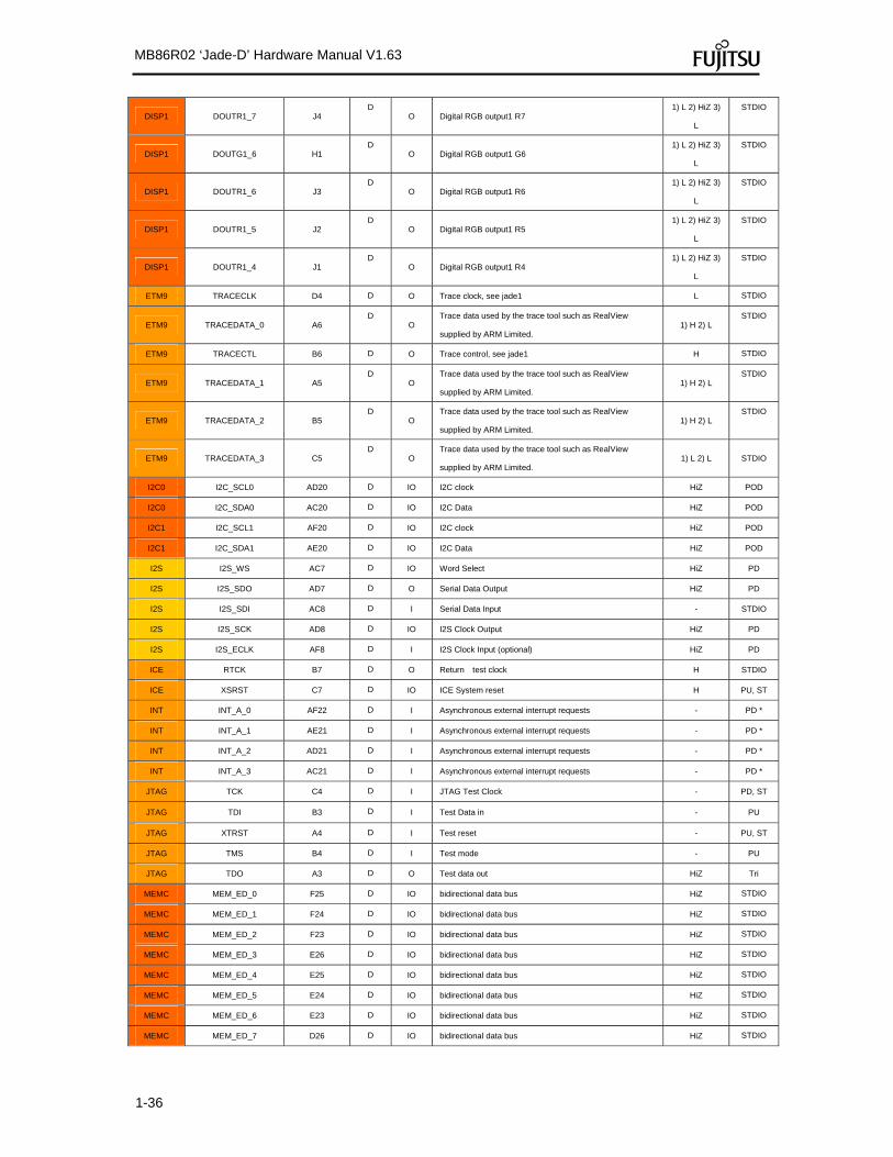
1-36
MB86R02 ‘Jade-D’ Hardware Manual V1.63
DISP1 DOUTR1_7 J4 D
O Digital RGB output1 R7 1) L 2) HiZ 3)
L
STDIO
DISP1 DOUTG1_6 H1 D
O Digital RGB output1 G6 1) L 2) HiZ 3)
L
STDIO
DISP1 DOUTR1_6 J3 D
O Digital RGB output1 R6 1) L 2) HiZ 3)
L
STDIO
DISP1 DOUTR1_5 J2 D
O Digital RGB output1 R5 1) L 2) HiZ 3)
L
STDIO
DISP1 DOUTR1_4 J1 D
O Digital RGB output1 R4 1) L 2) HiZ 3)
L
STDIO
ETM9 TRACECLK D4 D O Trace clock, see jade1 L STDIO
ETM9 TRACEDATA_0 A6 D
O Trace data used by the trace tool such as RealView
supplied by ARM Limited. 1) H 2) L
STDIO
ETM9 TRACECTL B6 D O Trace control, see jade1 H STDIO
ETM9 TRACEDATA_1 A5 D
O Trace data used by the trace tool such as RealView
supplied by ARM Limited. 1) H 2) L
STDIO
ETM9 TRACEDATA_2 B5 D
O Trace data used by the trace tool such as RealView
supplied by ARM Limited. 1) H 2) L
STDIO
ETM9 TRACEDATA_3 C5 D
O Trace data used by the trace tool such as RealView
supplied by ARM Limited. 1) L 2) L STDIO
I2C0 I2C_SCL0 AD20 D IO I2C clock HiZ POD
I2C0 I2C_SDA0 AC20 D IO I2C Data HiZ POD
I2C1 I2C_SCL1 AF20 D IO I2C clock HiZ POD
I2C1 I2C_SDA1 AE20 D IO I2C Data HiZ POD
I2S I2S_WS AC7 D IO Word Select HiZ PD
I2S I2S_SDO AD7 D O Serial Data Output HiZ PD
I2S I2S_SDI AC8 D I Serial Data Input - STDIO
I2S I2S_SCK AD8 D IO I2S Clock Output HiZ PD
I2S I2S_ECLK AF8 D I I2S Clock Input (optional) HiZ PD
ICE RTCK B7 D O Return test clock H STDIO
ICE XSRST C7 D IO ICE System reset H PU, ST
INT INT_A_0 AF22 D I Asynchronous external interrupt requests - PD *
INT INT_A_1 AE21 D I Asynchronous external interrupt requests - PD *
INT INT_A_2 AD21 D I Asynchronous external interrupt requests - PD *
INT INT_A_3 AC21 D I Asynchronous external interrupt requests - PD *
JTAG TCK C4 D I JTAG Test Clock - PD, ST
JTAG TDI B3 D I Test Data in - PU
JTAG XTRST A4 D I Test reset - PU, ST
JTAG TMS B4 D I Test mode - PU
JTAG TDO A3 D O Test data out HiZ Tri
MEMC MEM_ED_0 F25 D IO bidirectional data bus HiZ STDIO
MEMC MEM_ED_1 F24 D IO bidirectional data bus HiZ STDIO
MEMC MEM_ED_2 F23 D IO bidirectional data bus HiZ STDIO
MEMC MEM_ED_3 E26 D IO bidirectional data bus HiZ STDIO
MEMC MEM_ED_4 E25 D IO bidirectional data bus HiZ STDIO
MEMC MEM_ED_5 E24 D IO bidirectional data bus HiZ STDIO
MEMC MEM_ED_6 E23 D IO bidirectional data bus HiZ STDIO
MEMC MEM_ED_7 D26 D IO bidirectional data bus HiZ STDIO

1-37
MB86R02 ‘Jade-D’ Hardware Manual V1.63
MEMC MEM_ED_8 D25 D IO bidirectional data bus HiZ STDIO
MEMC MEM_ED_9 D24 D IO bidirectional data bus HiZ STDIO
MEMC MEM_ED_10 D23 D IO bidirectional data bus HiZ STDIO
MEMC MEM_ED_11 C26 D IO bidirectional data bus HiZ STDIO
MEMC MEM_ED_12 C25 D IO bidirectional data bus HiZ STDIO
MEMC MEM_ED_13 C24 D IO bidirectional data bus HiZ STDIO
MEMC MEM_ED_14 B25 D IO bidirectional data bus HiZ STDIO
MEMC MEM_ED_15 B24 D IO bidirectional data bus HiZ STDIO
MEMC MEM_EA_1 A24 D O Address bus L STDIO
MEMC MEM_EA_2 C23 D O Address bus L STDIO
MEMC MEM_EA_3 B23 D O Address bus L STDIO
MEMC MEM_EA_4 A23 D O Address bus L STDIO
MEMC MEM_EA_5 D22 D O Address bus L STDIO
MEMC MEM_EA_6 C22 D O Address bus L STDIO
MEMC MEM_EA_7 B22 D O Address bus L STDIO
MEMC MEM_EA_8 A22 D O Address bus L STDIO
MEMC MEM_EA_9 D21 D O Address bus L STDIO
MEMC MEM_EA_10 C21 D O Address bus L STDIO
MEMC MEM_EA_11 B21 D O Address bus L STDIO
MEMC MEM_EA_12 A21 D O Address bus L STDIO
MEMC MEM_EA_13 D20 D O Address bus L STDIO
MEMC MEM_EA_14 C20 D O Address bus L STDIO
MEMC MEM_EA_15 B20 D O Address bus L STDIO
MEMC MEM_EA_16 A20 D O Address bus L STDIO
MEMC MEM_EA_17 D19 D O Address bus L STDIO
MEMC MEM_EA_18 C19 D O Address bus L STDIO
MEMC MEM_EA_19 B19 D O Address bus L STDIO
MEMC MEM_EA_20 A19 D O Address bus L STDIO
MEMC MEM_EA_21 D18 D O Address bus L STDIO
MEMC MEM_EA_22 C18 D O Address bus L STDIO
MEMC MEM_EA_23 B18 D O Address bus L STDIO
MEMC MEM_EA_24 D17 D O Address bus L STDIO
MEMC MEM_XWR_0 C17 D O Write strobe, see jade1 H STDIO
MEMC MEM_XWR_1 B17 D O Write strobe, see jade1 H STDIO
MEMC MEM_XRD A17 D O Read Strobe H STDIO
MEMC MEM_XCS_0 D16 D O Chip Select 0 H STDIO
MEMC MEM_XCS_2 C16 D O Chip Select 2 H STDIO
MEMC MEM_XCS_4 B16 D O Chip Select 4 H STDIO
MEMC MEM_RDY D15 D I Raedy input for slow devices H STDIO
MLB MLB_SIG AE6 D IO Media LB Control Pin HiZ STDIO
MLB MLB_DAT AF6 D IO Media LB Data Pin HiZ STDIO
MLB MLB_CLK AE7 D I Media LB Clock Pin - PD *
MPX TEST MPX_MODE_1_0 K4 D I Multiplex Mode Pin - STDIO
MPX TEST MPX_MODE_1_1 K3 D I Multiplex Mode Pin - STDIO
MPX TEST MPX_MODE_5_1 U3 D I Multiplex Mode Pin - STDIO
MPX TEST MPX_MODE_5_0 U4 D I Multiplex Mode Pin - STDIO
MPX TEST VPD AF12 D I Multiplex Mode Pin - PD

1-38
MB86R02 ‘Jade-D’ Hardware Manual V1.63
MPX TEST TESTMODE_3 AE12 D I Test Mode Pin - STDIO
MPX TEST TESTMODE_2 AD12 D
I Test Mode Pin, In Functional Mode this pin selects the
Endianess: Low: Little endian, High: Big endian -
STDIO
MPX TEST TESTMODE_1 AE15 D I Test Mode Pin, in functionalk Mode PLLBYPASS - STDIO
MPX TEST TESTMODE_0 AD15 D I Test Mode Pin - STDIO
MPX TEST JTAGSEL E8 D I JTAG Selector (0 = Fujitsu TAP Controller, 1 = ARM Tap
Controller) -
STDIO
MPX TEST TESTMODE_4 C6 D I Test Mode Pin - STDIO
PLL #PLLVDD E14 A I PLL Supply: 1,2 Volt / In case it is derived from core supply
a protection by a filter is recommended. L
STDIO
PLL #PLLVSS E13 A I PLL Supply (seperated ground plane recommented,
connection via filter to digital ground) L
STDIO
PWM PWM_O3 AF10 D O PWM Output L PD
PWM PWM_O2 AE10 D O PWM Output - PD
PWM PWM_O1 AD10 D O PWM Output L PD
PWM PWM_O0 AC10 D O PWM Output - PD
SPI(m)0 SPI_DI0 AF18 D I SPI0 Master Data Input (MISO) HiZ STDIO
SPI(m)0 SPI_DO0 AE18 D O SPI0 Master Data Output (MOSI) - STDIO
SPI(m)0 SPI_SS0 AD18 D O SPI0 Master Slave Select - STDIO
SPI(m)0 SPI_SCK0 AC18 D O SPI0 Master serial clock - STDIO
SPI(m)1 SPI_DI1 AF19 D I SPI1 Master Data Input (MISO) HiZ STDIO
SPI(m)1 SPI_DO1 AE19 D O SPI1 Master Data Output (MOSI) - STDIO
SPI(m)1 SPI_SS1 AD19 D O SPI1 Master Slave Select L STDIO
SPI(m)1 SPI_SCK1 AC19 D O SPI1 Master serial clock L STDIO
SPI(s)Host HOST_SPI_SCK AF11 D I HOST SPI Clock HiZ PU *
SPI(s)Host HOST_SPI_DI AE11 D I HOST SPI Data Input (MOSI) HiZ PU *
SPI(s)Host HOST_SPI_DO AD11 D O HOST SPI Data Output (MISO) L STDIO
SPI(s)Host HOST_SPI_SS AC11 D I HOST SPI Slave Select HiZ PU *
SSCG #SSCGVDD C14 A I SSCG Supply: 1,2 Volt / In case it is derived from core
supply a protection by a filter is recommended. L
STDIO
SSCG #SSCGVSS D14 A I SSCG Supply (seperated ground plane recommented,
connection via filter to digital ground) L
STDIO
SYSTEM PLLTDTRST E4 D
I Test pin
Pull up the pin to VDDE, via high resistance - PU *
SYSTEM CLK_SEL K2 D I Select Pin for emb. Crystal CLK or ECLK - STDIO
SYSTEM ECLK A16 D I External Clock Source (selected by CLK_SEL) - STDIO
SYSTEM CRIPM0 A15 D I PLLMODE setting - STDIO
SYSTEM CRIPM1 B15 D I PLLMODE setting - STDIO
SYSTEM CRIPM2 C15 D I PLLMODE setting - STDIO
SYSTEM CRIPM3 B14 D I PLLMODE setting - STDIO
SYSTEM OSC_FILTER C12 D I characteristic of post-oscillator filter - STDIO
SYSTEM XTAL0 A11 A I Crystal reference L STDIO
SYSTEM XTAL1 B11 A I Crystal reference L STDIO
SYSTEM OSC_MODE1 B8 D I oscillator mode 1 - STDIO
SYSTEM OSC_BIAS0 C8 D I Oscillator bias level 0 - STDIO
SYSTEM OSC_BIAS1 D8 D I Oscillator bias level 1 - STDIO
SYSTEM OSC_MODE0 A7 D I oscillator mode 0 - STDIO
SYSTEM XRST D6 D I System Reset - ST

1-39
MB86R02 ‘Jade-D’ Hardware Manual V1.63
SYSTEM VINITHI D5 D I Boot high address - STDIO
UART0 UART_SIN0 AF16 D I UART0 serial input 1) HiZ 2) H PD *
UART0 UART_SOUT0 AE16 D O UART0 serial output 1) H 2) H STDIO
UART0 UART_XCTS0 AD16 D I UART0 Clear to send 1) HiZ 2) L PD
UART0 UART_XRTS0 AC16 D O UART0 Request to send 1) H 2) L STDIO
UART1 UART_SIN1 AF17 D I UART1 serial input HiZ PD
UART1 UART_SOUT1 AE17 D O UART1 serial output H STDIO
UART2 UART_SIN2 AD17 D I UART2 serial input HiZ PD *
UART2 UART_SOUT2 AC17 D O UART2 serial output H STDIO
IO: A = Analog
D = Digital
I = Input
O = Output
IO = Bidirectional (Input/Output)
Initial state after reset: H = High
L = Low
HiZ = High-Impedance
1) = First hardware multiplex function
2) = Second hardware multiplex function
3) = Third hardware multiplex function
Type: PD = Pull-Down
PU = Pull-Up
ST = Schmitt Trigger
CLK = Clock
POD = Pseudo Open-Drain
Tri = Tri-State
MSIO = Multistandard IO (RSDS, LVTTL - no PU or PD for both)
STDIO = Standard IO cell (no PU or PD)
* Note concerning changes for MB86R02 'Jade-D' (ES2) Please note that the pins described in the above table have been modified in version ES2 of the MBR02 'Jade-D' device (a pull-up or pull-down has been added). See also Addendum.

1-40
MB86R02 ‘Jade-D’ Hardware Manual V1.63
Unused Pins This section is intended for PCB designers and describes the way in which pins, whose functionality is not required (used) should be connected (pulled up, pulled down or left open/'floating') in the layout. A 'high resistance' as referred to in the table is typically: 4k7Ohms The term n/a stands for 'not applicable' and refers to some pins whose functionality is required for the use of the chip (i.e. they can not be unused). Power and ground pins are not described as these must be connected to the corresponding signal. Ext PinName Description Unused Pin
usage
AD_VRH0 Reference voltage "H" input, for channel 0 and 2 Connect to VSS
AD_VIN0 A/D analog input, channel 0 Connect to VSS
AD_VR0 Reference output, for channel 0 and 2 Connect to VSS
AD_VRL0 Reference voltage "L" input, for channel 0 and 2 Connect to VSS
AD_VRH1 Reference voltage "H" input, for channel 1 and 3 Connect to VSS
AD_VIN2 A/D analog input, channel 2 Connect to VSS
AD_VR1 Reference output, for channel 1 and 3 Connect to VSS
AD_VRL1 Reference voltage "L" input,, for channel 1 and 3 Connect to VSS
AD_VIN1 A/D analog input, channel 1 Connect to VSS
AD_VIN3 A/D analog input, channel 3 Connect to VSS
SDOUT1M Serial Data Output 1 (negative) Keep the pin open
SDOUT1P Serial Data Output 1 (positive) Keep the pin open
SDIN1M Serial Data Input 1 (negative) Keep the pin open
VCM1 Common Mode decoupling for input 1 Keep the pin open
SDIN1P Serial Data Input 1 (positive) Keep the pin open
RREF Reference resistor for bias Keep the pin open
XTAL0 Crystal reference Keep the pin open
XTAL1 Crystal reference Keep the pin open
ATST Analog test port Keep the pin open
SDIN0M Serial Data Input 0 (negative) Keep the pin open
VCM0 Common Mode decoupling for input 0 Keep the pin open
SDIN0P Serial Data Input 0 (positive) Keep the pin open
SDOUT0M Serial Data Output 0 (negative) Keep the pin open
SDOUT0P Serial Data Output 0 (positive) Keep the pin open
CAN_RX1 CAN Reception 1 Keep the pin open
CAN_TX1 CAN Transmission 1 Keep the pin open
CAN_RX0 CAN Reception 0 Keep the pin open
CAN_TX0 CAN Transmission 0 Keep the pin open
VINFID0 Video input 0 field identification signal Keep the pin open
VIN0_4 Video Capture Data Input 0 bit 4 Keep the pin open
VIN0_5 Video Capture Data Input 0 bit 5 Keep the pin open
VIN0_6 Video Capture Data Input 0 bit 6 Keep the pin open
VIN0_7 Video Capture Data Input 0 bit 7 Keep the pin open
VIN0_0 Video Capture Data Input 0 bit 0 Keep the pin open
VIN0_1 Video Capture Data Input 0 bit 1 Keep the pin open
VIN0_2 Video Capture Data Input 0 bit 2 Keep the pin open
VIN0_3 Video Capture Data Input 0 bit 3 Keep the pin open
CCLK0 Video Capture 0 Clock Keep the pin open
VINHSYNC0 Video Capture 0 Horizontal Synchronisation Keep the pin open
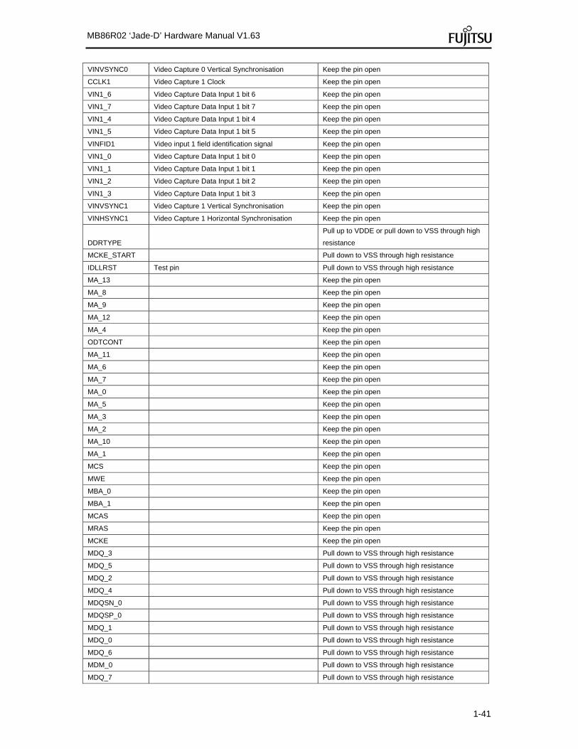
1-41
MB86R02 ‘Jade-D’ Hardware Manual V1.63
VINVSYNC0 Video Capture 0 Vertical Synchronisation Keep the pin open
CCLK1 Video Capture 1 Clock Keep the pin open
VIN1_6 Video Capture Data Input 1 bit 6 Keep the pin open
VIN1_7 Video Capture Data Input 1 bit 7 Keep the pin open
VIN1_4 Video Capture Data Input 1 bit 4 Keep the pin open
VIN1_5 Video Capture Data Input 1 bit 5 Keep the pin open
VINFID1 Video input 1 field identification signal Keep the pin open
VIN1_0 Video Capture Data Input 1 bit 0 Keep the pin open
VIN1_1 Video Capture Data Input 1 bit 1 Keep the pin open
VIN1_2 Video Capture Data Input 1 bit 2 Keep the pin open
VIN1_3 Video Capture Data Input 1 bit 3 Keep the pin open
VINVSYNC1 Video Capture 1 Vertical Synchronisation Keep the pin open
VINHSYNC1 Video Capture 1 Horizontal Synchronisation Keep the pin open
DDRTYPE
Pull up to VDDE or pull down to VSS through high
resistance
MCKE_START Pull down to VSS through high resistance
IDLLRST Test pin Pull down to VSS through high resistance
MA_13 Keep the pin open
MA_8 Keep the pin open
MA_9 Keep the pin open
MA_12 Keep the pin open
MA_4 Keep the pin open
ODTCONT Keep the pin open
MA_11 Keep the pin open
MA_6 Keep the pin open
MA_7 Keep the pin open
MA_0 Keep the pin open
MA_5 Keep the pin open
MA_3 Keep the pin open
MA_2 Keep the pin open
MA_10 Keep the pin open
MA_1 Keep the pin open
MCS Keep the pin open
MWE Keep the pin open
MBA_0 Keep the pin open
MBA_1 Keep the pin open
MCAS Keep the pin open
MRAS Keep the pin open
MCKE Keep the pin open
MDQ_3 Pull down to VSS through high resistance
MDQ_5 Pull down to VSS through high resistance
MDQ_2 Pull down to VSS through high resistance
MDQ_4 Pull down to VSS through high resistance
MDQSN_0 Pull down to VSS through high resistance
MDQSP_0 Pull down to VSS through high resistance
MDQ_1 Pull down to VSS through high resistance
MDQ_0 Pull down to VSS through high resistance
MDQ_6 Pull down to VSS through high resistance
MDM_0 Pull down to VSS through high resistance
MDQ_7 Pull down to VSS through high resistance

1-42
MB86R02 ‘Jade-D’ Hardware Manual V1.63
VREF0 Connect to DDRVDE/2[V] reference voltage
MDQ_11 Pull down to VSS through high resistance
MDQ_10 Pull down to VSS through high resistance
MDQ_13 Pull down to VSS through high resistance
MDQ_12 Pull down to VSS through high resistance
MDQSN_1 Pull down to VSS through high resistance
MDQSP_1 Pull down to VSS through high resistance
MDQ_9 Pull down to VSS through high resistance
MDQ_8 Pull down to VSS through high resistance
MDQ_14 Pull down to VSS through high resistance
MDM_1 Pull down to VSS through high resistance
MDQ_15 Pull down to VSS through high resistance
MCKN Keep the pin open
MCKP Keep the pin open
OCD Keep the pin open
ODT Keep the pin open
MDQ_19 Pull down to VSS through high resistance
MDQ_18 Pull down to VSS through high resistance
MDQ_21 Pull down to VSS through high resistance
MDQ_20 Pull down to VSS through high resistance
MDQSN_2 Pull down to VSS through high resistance
MDQSP_2 Pull down to VSS through high resistance
MDQ_17 Pull down to VSS through high resistance
MDQ_16 Pull down to VSS through high resistance
MDQ_22 Pull down to VSS through high resistance
MDM_2 Pull down to VSS through high resistance
MDQ_23 Pull down to VSS through high resistance
VREF1 Connect to DDRVDE/2[V]Reference voltage
MDQ_27 Pull down to VSS through high resistance
MDQ_26 Pull down to VSS through high resistance
MDQ_29 Pull down to VSS through high resistance
MDQ_25 Pull down to VSS through high resistance
MDQSN_3 Pull down to VSS through high resistance
MDQSP_3 Pull down to VSS through high resistance
MDQ_28 Pull down to VSS through high resistance
MDQ_24 Pull down to VSS through high resistance
MDQ_30 Pull down to VSS through high resistance
MDM_3 Pull down to VSS through high resistance
MDQ_31 Pull down to VSS through high resistance
DISP0P
Display 0 output channel 0p, Default=DOUTR0_0
(TTL-mode)
Pull up to VDDE or pull down to VSS through high
resistance
DISP0N
Display 0 output channel 0n,
Default=DOUTR0_1 (TTL-mode)
Pull up to VDDE or pull down to VSS through high
resistance
DISP1P
Display 0 output channel 1p,
Default=DOUTR0_2 (TTL-mode)
Pull up to VDDE or pull down to VSS through high
resistance
DISP1N
Display 0 output channel 1n,
Default=DOUTR0_3 (TTL-mode)
Pull up to VDDE or pull down to VSS through high
resistance
DISP2P
Display 0 output channel 2p,
Default=DOUTR0_4 (TTL-mode)
Pull up to VDDE or pull down to VSS through high
resistance
DISP2N Display 0 output channel 2n, Pull up to VDDE or pull down to VSS through high

1-43
MB86R02 ‘Jade-D’ Hardware Manual V1.63
Default=DOUTR0_5 (TTL-mode) resistance
DISP3P
Display 0 output channel 3p,
Default=DOUTR0_6 (TTL-mode)
Pull up to VDDE or pull down to VSS through high
resistance
DISP3N
Display 0 output channel 3n,
Default=DOUTR0_7 (TTL-mode)
Pull up to VDDE or pull down to VSS through high
resistance
DISP4P
Display 0 output channel 4p,
Default=DOUTG0_0 (TTL-mode)
Pull up to VDDE or pull down to VSS through high
resistance
DISP4N
Display 0 output channel 4n,
Default=DOUTG0_1 (TTL-mode)
Pull up to VDDE or pull down to VSS through high
resistance
DISP5P
Display 0 output channel 5p,
Default=DOUTG0_2 (TTL-mode)
Pull up to VDDE or pull down to VSS through high
resistance
DISP5N
Display 0 output channel 5n,
Default=DOUTG0_3 (TTL-mode)
Pull up to VDDE or pull down to VSS through high
resistance
DISP6P
Display 0 output channel 6p,
Default=DOUTG0_4 (TTL-mode)
Pull up to VDDE or pull down to VSS through high
resistance
DISP6N
Display 0 output channel 6n,
Default=DOUTG0_5 (TTL-mode)
Pull up to VDDE or pull down to VSS through high
resistance
DISP7P
Display 0 output channel 7p,
Default=DOUTG0_6 (TTL-mode)
Pull up to VDDE or pull down to VSS through high
resistance
DISP7N
Display 0 output channel 7n,
Default=DOUTG0_7 (TTL-mode)
Pull up to VDDE or pull down to VSS through high
resistance
DISP8P
Display 0 output channel 8p,
Default=DOUTB0_0 (TTL-mode)
Pull up to VDDE or pull down to VSS through high
resistance
DISP8N
Display 0 output channel 8n,
Default=DOUTB0_1 (TTL-mode)
Pull up to VDDE or pull down to VSS through high
resistance
DISP9P
Display 0 output channel 9p,
Default=DOUTB0_2 (TTL-mode)
Pull up to VDDE or pull down to VSS through high
resistance
DISP9N
Display 0 output channel 9n,
Default=DOUTB0_3 (TTL-mode)
Pull up to VDDE or pull down to VSS through high
resistance
DISP10P
Display 0 output channel 10p,
Default=DOUTB0_4 (TTL-mode)
Pull up to VDDE or pull down to VSS through high
resistance
DISP10N
Display 0 output channel 10n,
Default=DOUTB0_5 (TTL-mode)
Pull up to VDDE or pull down to VSS through high
resistance
DISP11P
Display 0 output channel 11p,
Default=DOUTB0_6 (TTL-mode)
Pull up to VDDE or pull down to VSS through high
resistance
DISP11N
Display 0 output channel 11n,
Default=DOUTB0_7 (TTL-mode)
Pull up to VDDE or pull down to VSS through high
resistance
DCLKP
Display 0 Clock Output CLKp,
Default=DCLK0UT0 (TTL-mode)
Pull up to VDDE or pull down to VSS through high
resistance
DCLKN
Display 0 Clock Output CLKn,
Default=DCLK0UT0 (TTL-mode)
Pull up to VDDE or pull down to VSS through high
resistance
TSG_4 TCON Timing Signal 4 Keep the pin open
VSYNC0
TCON Bypass: Video output interface 0 vertical
sync output vertical sync input in external sync
mode, TCON: TSG_1
Pull up to VDDE or pull down to VSS through high
resistance
DE0
TCON Bypass: DE/CSYNC of DISPL0,
TCON:TSG_2
Pull up to VDDE or pull down to VSS through high
resistance
GV0
TCON Bypass: Video output interface 0
graphics/video switch, TCON: TSG_3
Pull up to VDDE or pull down to VSS through high
resistance
HSYNC0
TCON Bypass: Video output interface 0 horizontal
sync output Horizontal sync input in external sync
Pull up to VDDE or pull down to VSS through high
resistance
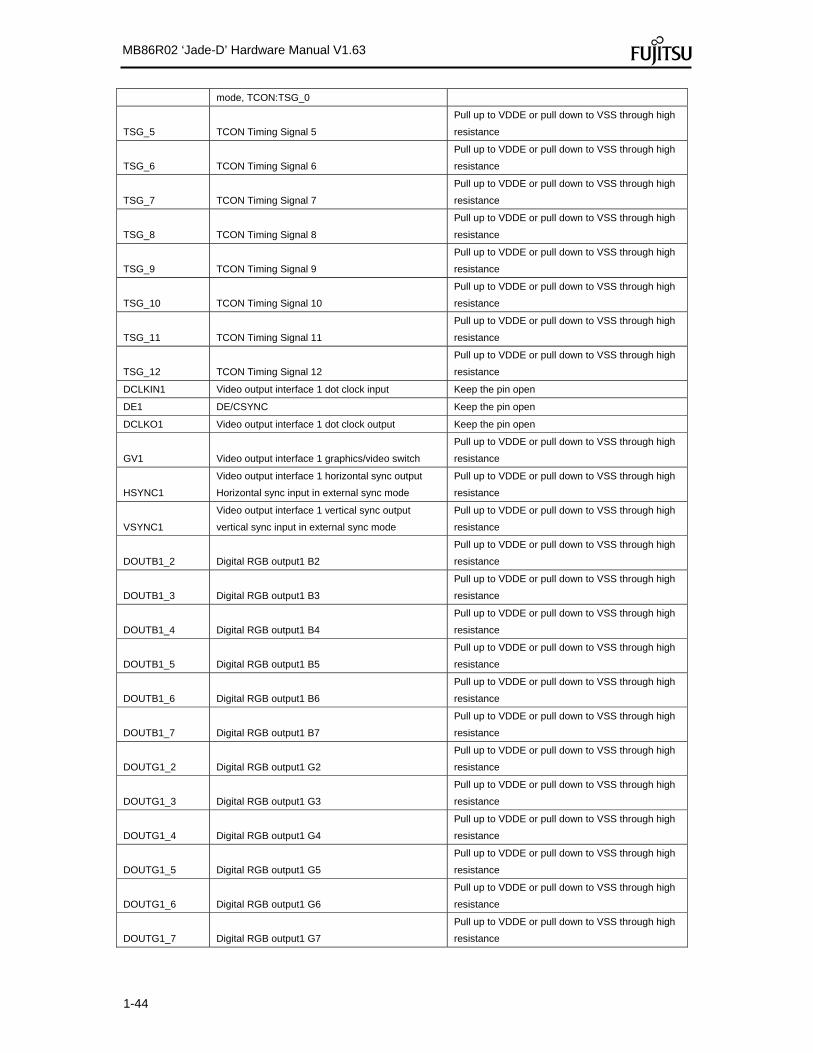
1-44
MB86R02 ‘Jade-D’ Hardware Manual V1.63
mode, TCON:TSG_0
TSG_5 TCON Timing Signal 5
Pull up to VDDE or pull down to VSS through high
resistance
TSG_6 TCON Timing Signal 6
Pull up to VDDE or pull down to VSS through high
resistance
TSG_7 TCON Timing Signal 7
Pull up to VDDE or pull down to VSS through high
resistance
TSG_8 TCON Timing Signal 8
Pull up to VDDE or pull down to VSS through high
resistance
TSG_9 TCON Timing Signal 9
Pull up to VDDE or pull down to VSS through high
resistance
TSG_10 TCON Timing Signal 10
Pull up to VDDE or pull down to VSS through high
resistance
TSG_11 TCON Timing Signal 11
Pull up to VDDE or pull down to VSS through high
resistance
TSG_12 TCON Timing Signal 12
Pull up to VDDE or pull down to VSS through high
resistance
DCLKIN1 Video output interface 1 dot clock input Keep the pin open
DE1 DE/CSYNC Keep the pin open
DCLKO1 Video output interface 1 dot clock output Keep the pin open
GV1 Video output interface 1 graphics/video switch
Pull up to VDDE or pull down to VSS through high
resistance
HSYNC1
Video output interface 1 horizontal sync output
Horizontal sync input in external sync mode
Pull up to VDDE or pull down to VSS through high
resistance
VSYNC1
Video output interface 1 vertical sync output
vertical sync input in external sync mode
Pull up to VDDE or pull down to VSS through high
resistance
DOUTB1_2 Digital RGB output1 B2
Pull up to VDDE or pull down to VSS through high
resistance
DOUTB1_3 Digital RGB output1 B3
Pull up to VDDE or pull down to VSS through high
resistance
DOUTB1_4 Digital RGB output1 B4
Pull up to VDDE or pull down to VSS through high
resistance
DOUTB1_5 Digital RGB output1 B5
Pull up to VDDE or pull down to VSS through high
resistance
DOUTB1_6 Digital RGB output1 B6
Pull up to VDDE or pull down to VSS through high
resistance
DOUTB1_7 Digital RGB output1 B7
Pull up to VDDE or pull down to VSS through high
resistance
DOUTG1_2 Digital RGB output1 G2
Pull up to VDDE or pull down to VSS through high
resistance
DOUTG1_3 Digital RGB output1 G3
Pull up to VDDE or pull down to VSS through high
resistance
DOUTG1_4 Digital RGB output1 G4
Pull up to VDDE or pull down to VSS through high
resistance
DOUTG1_5 Digital RGB output1 G5
Pull up to VDDE or pull down to VSS through high
resistance
DOUTG1_6 Digital RGB output1 G6
Pull up to VDDE or pull down to VSS through high
resistance
DOUTG1_7 Digital RGB output1 G7
Pull up to VDDE or pull down to VSS through high
resistance

1-45
MB86R02 ‘Jade-D’ Hardware Manual V1.63
DOUTR1_2 Digital RGB output1 R2
Pull up to VDDE or pull down to VSS through high
resistance
DOUTR1_3 Digital RGB output1 R3
Pull up to VDDE or pull down to VSS through high
resistance
DOUTR1_4 Digital RGB output1 R4
Pull up to VDDE or pull down to VSS through high
resistance
DOUTR1_5 Digital RGB output1 R5
Pull up to VDDE or pull down to VSS through high
resistance
DOUTR1_6 Digital RGB output1 R6
Pull up to VDDE or pull down to VSS through high
resistance
DOUTR1_7 Digital RGB output1 R7
Pull up to VDDE or pull down to VSS through high
resistance
I2C_SCL0
Pull up to VDDE or pull down to VSS through high
resistance
I2C_SDA0
Pull up to VDDE or pull down to VSS through high
resistance
I2C_SCL1
Pull up to VDDE or pull down to VSS through high
resistance
I2C_SDA1
Pull up to VDDE or pull down to VSS through high
resistance
I2S_SDO Serial Data Output Keep the pin open
I2S_WS Word Select Keep the pin open
I2S_ECLK I2S Clock Input (optional)
Pull up to VDDE or pull down to VSS through high
resistance
I2S_SCK I2S Clock Output Keep the pin open
I2S_SDI Serial Data Input
Pull up to VDDE or pull down to VSS through high
resistance
INT_A_3 Keep the pin open
INT_A_2 Keep the pin open
INT_A_1 Keep the pin open
INT_A_0 Keep the pin open
TDO Keep the pin open
TRACECLK
Pull up to VDDE or pull down to VSS through high
resistance
TDI Keep the pin open
JTAGSEL
JTAG Selector (0 = Fujitsu TAP Controller, 1 =
ARM Tap Controller) Pull it down to VSS, via high resistance
RTCK Return test clock Keep the pin open
TRACEDATA_0 Trace data used by the trace tool such as
RealView supplied by ARM Limited.
Pull up to VDDE or pull down to VSS through high
resistance.
If the TRACEDATA_x pins (C5, B5, A5, A6) are
unused in multiplex mode #3, then an external
termination is not required because the pins are in
output mode. To make sure that the pins do not
oscillate, check PWMxSR[0] = 0 (i.e. Stop PWM) is
set.
TRACECTL Keep the pin open
XSRST ICE System reset Keep the pin open
TRACEDATA_1
Trace data used by the trace tool such as
RealView supplied by ARM Limited.
Pull up to VDDE or pull down to VSS through high
resistance. See also TRACEDATA_0.

1-46
MB86R02 ‘Jade-D’ Hardware Manual V1.63
TRACEDATA_2
Trace data used by the trace tool such as
RealView supplied by ARM Limited.
Pull up to VDDE or pull down to VSS through high
resistance. See also TRACEDATA_0.
TRACEDATA_3
Trace data used by the trace tool such as
RealView supplied by ARM Limited.
Pull up to VDDE or pull down to VSS through high
resistance. See also TRACEDATA_0.
TMS Keep the pin open
TCK JTAG Test Clock Keep the pin open
MEM_ED_0
Pull up to VDDE or pull down to VSS through high
resistance
MEM_ED_1
Pull up to VDDE or pull down to VSS through high
resistance
MEM_ED_2
Pull up to VDDE or pull down to VSS through high
resistance
MEM_ED_3
Pull up to VDDE or pull down to VSS through high
resistance
MEM_ED_4
Pull up to VDDE or pull down to VSS through high
resistance
MEM_ED_5
Pull up to VDDE or pull down to VSS through high
resistance
MEM_ED_6
Pull up to VDDE or pull down to VSS through high
resistance
MEM_ED_7
Pull up to VDDE or pull down to VSS through high
resistance
MEM_ED_8
Pull up to VDDE or pull down to VSS through high
resistance
MEM_ED_9
Pull up to VDDE or pull down to VSS through high
resistance
MEM_ED_10
Pull up to VDDE or pull down to VSS through high
resistance
MEM_ED_11
Pull up to VDDE or pull down to VSS through high
resistance
MEM_ED_12
Pull up to VDDE or pull down to VSS through high
resistance
MEM_ED_13
Pull up to VDDE or pull down to VSS through high
resistance
MEM_ED_14
Pull up to VDDE or pull down to VSS through high
resistance
MEM_ED_15
Pull up to VDDE or pull down to VSS through high
resistance
MEM_EA_1
Pull up to VDDE or pull down to VSS through high
resistance
MEM_EA_2
Pull up to VDDE or pull down to VSS through high
resistance
MEM_EA_3
Pull up to VDDE or pull down to VSS through high
resistance
MEM_EA_4
Pull up to VDDE or pull down to VSS through high
resistance
MEM_EA_5
Pull up to VDDE or pull down to VSS through high
resistance
MEM_EA_6
Pull up to VDDE or pull down to VSS through high
resistance
MEM_EA_7 Pull up to VDDE or pull down to VSS through high
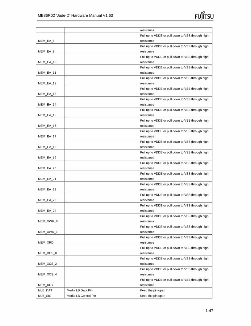
1-47
MB86R02 ‘Jade-D’ Hardware Manual V1.63
resistance
MEM_EA_8
Pull up to VDDE or pull down to VSS through high
resistance
MEM_EA_9
Pull up to VDDE or pull down to VSS through high
resistance
MEM_EA_10
Pull up to VDDE or pull down to VSS through high
resistance
MEM_EA_11
Pull up to VDDE or pull down to VSS through high
resistance
MEM_EA_12
Pull up to VDDE or pull down to VSS through high
resistance
MEM_EA_13
Pull up to VDDE or pull down to VSS through high
resistance
MEM_EA_14
Pull up to VDDE or pull down to VSS through high
resistance
MEM_EA_15
Pull up to VDDE or pull down to VSS through high
resistance
MEM_EA_16
Pull up to VDDE or pull down to VSS through high
resistance
MEM_EA_17
Pull up to VDDE or pull down to VSS through high
resistance
MEM_EA_18
Pull up to VDDE or pull down to VSS through high
resistance
MEM_EA_19
Pull up to VDDE or pull down to VSS through high
resistance
MEM_EA_20
Pull up to VDDE or pull down to VSS through high
resistance
MEM_EA_21
Pull up to VDDE or pull down to VSS through high
resistance
MEM_EA_22
Pull up to VDDE or pull down to VSS through high
resistance
MEM_EA_23
Pull up to VDDE or pull down to VSS through high
resistance
MEM_EA_24
Pull up to VDDE or pull down to VSS through high
resistance
MEM_XWR_0
Pull up to VDDE or pull down to VSS through high
resistance
MEM_XWR_1
Pull up to VDDE or pull down to VSS through high
resistance
MEM_XRD
Pull up to VDDE or pull down to VSS through high
resistance
MEM_XCS_0
Pull up to VDDE or pull down to VSS through high
resistance
MEM_XCS_2
Pull up to VDDE or pull down to VSS through high
resistance
MEM_XCS_4
Pull up to VDDE or pull down to VSS through high
resistance
MEM_RDY
Pull up to VDDE or pull down to VSS through high
resistance
MLB_DAT Media LB Data Pin Keep the pin open
MLB_SIG Media LB Control Pin Keep the pin open
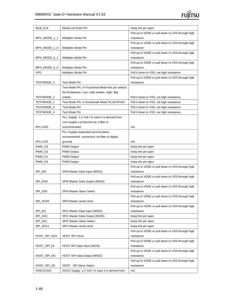
1-48
MB86R02 ‘Jade-D’ Hardware Manual V1.63
MLB_CLK Media LB Clock Pin Keep the pin open
MPX_MODE_1_1 Multiplex Mode Pin
Pull up to VDDE or pull down to VSS through high
resistance
MPX_MODE_1_0 Multiplex Mode Pin
Pull up to VDDE or pull down to VSS through high
resistance
MPX_MODE_5_1 Multiplex Mode Pin
Pull up to VDDE or pull down to VSS through high
resistance
MPX_MODE_5_0 Multiplex Mode Pin
Pull up to VDDE or pull down to VSS through high
resistance
VPD Multiplex Mode Pin Pull it down to VSS, via high resistance
TESTMODE_3 Test Mode Pin
Pull up to VDDE or pull down to VSS through high
resistance
TESTMODE_2
Test Mode Pin, In Functional Mode this pin selects
the Endianess: Low: Little endian, High: Big
endian Pull it down to VSS, via high resistance
TESTMODE_1 Test Mode Pin, in functionalk Mode PLLBYPASS Pull it down to VSS, via high resistance
TESTMODE_0 Test Mode Pin Pull it down to VSS, via high resistance
TESTMODE_4 Test Mode Pin Pull it down to VSS, via high resistance
#PLLVDD
PLL Supply: 1,2 Volt / In case it is derived from
core supply a protection by a filter is
recommended. n/a
#PLLVSS
PLL Supply (seperated ground plane
recommented, connection via filter to digital
ground) n/a
PWM_O3 PWM Output Keep the pin open
PWM_O2 PWM Output Keep the pin open
PWM_O1 PWM Output Keep the pin open
PWM_O0 PWM Output Keep the pin open
SPI_DI0 SPI0 Master Data Input (MISO)
Pull up to VDDE or pull down to VSS through high
resistance
SPI_DO0 SPI0 Master Data Output (MOSI)
Pull up to VDDE or pull down to VSS through high
resistance
SPI_SS0 SPI0 Master Slave Select
Pull up to VDDE or pull down to VSS through high
resistance
SPI_SCK0 SPI0 Master serial clock
Pull up to VDDE or pull down to VSS through high
resistance
SPI_DI1 SPI1 Master Data Input (MISO)
Pull up to VDDE or pull down to VSS through high
resistance
SPI_DO1 SPI1 Master Data Output (MOSI) Keep the pin open
SPI_SS1 SPI1 Master Slave Select Keep the pin open
SPI_SCK1 SPI1 Master serial clock Keep the pin open
HOST_SPI_SCK HOST SPI Clock
Pull up to VDDE or pull down to VSS through high
resistance
HOST_SPI_DI HOST SPI Data Input (MOSI)
Pull up to VDDE or pull down to VSS through high
resistance
HOST_SPI_DO HOST SPI Data Output (MISO)
Pull up to VDDE or pull down to VSS through high
resistance
HOST_SPI_SS HOST SPI Slave Select
Pull up to VDDE or pull down to VSS through high
resistance
#SSCGVDD SSCG Supply: 1,2 Volt / In case it is derived from n/a

1-49
MB86R02 ‘Jade-D’ Hardware Manual V1.63
core supply a protection by a filter is
recommended.
#SSCGVSS
SSCG Supply (seperated ground plane
recommented, connection via filter to digital
ground) n/a
VINITHI Connect to VSS
CLK_SEL Select Pin for emb. Crystal CLK or ECLK
Pull down to VSS through high resistance for
embedded OSC or
Pull up to VDDE through high resistance for
external OSC (clock input ECLK)
ECLK External Clock Source (selected by CLK_SEL)
Pull up to VDDE or pull down to VSS through high
resistance
CRIPM0
Pull up to VDDE or pull down to VSS through high
resistance
CRIPM1
Pull up to VDDE or pull down to VSS through high
resistance
CRIPM2
Pull up to VDDE or pull down to VSS through high
resistance
CRIPM3
Pull up to VDDE or pull down to VSS through high
resistance
OSC_FILTER characteristic of post-oscillator filter Connect to VDDE (3.3V) via a high resistance
OSC_MODE1 oscillator mode 1 Connect to VSS
OSC_BIAS0 Oscillator bias level 0 Connect to VSS
OSC_BIAS1 Oscillator bias level 1 Connect to VSS
OSC_MODE0 oscillator mode 0 Connect to VSS
XRST System Reset n/a
PLLTDTRST PLL Transition Delay Test Reset ???? Keep the pin open
XTRST Test reset n/a
UART_SIN0 UART0 serial input Keep the pin open
UART_SOUT0 UART0 serial output
Pull up to VDDE or pull down to VSS through high
resistance
UART_XCTS0 UART0 Clear to send Keep the pin open
UART_XRTS0 UART0 Request to send
Pull up to VDDE or pull down to VSS through high
resistance
UART_SIN1 UART1 serial input Keep the pin open
UART_SOUT1 UART1 serial output
Pull up to VDDE or pull down to VSS through high
resistance
UART_SIN2 UART2 serial input Keep the pin open
UART_SOUT2 UART2 serial output
Pull up to VDDE or pull down to VSS through high
resistance
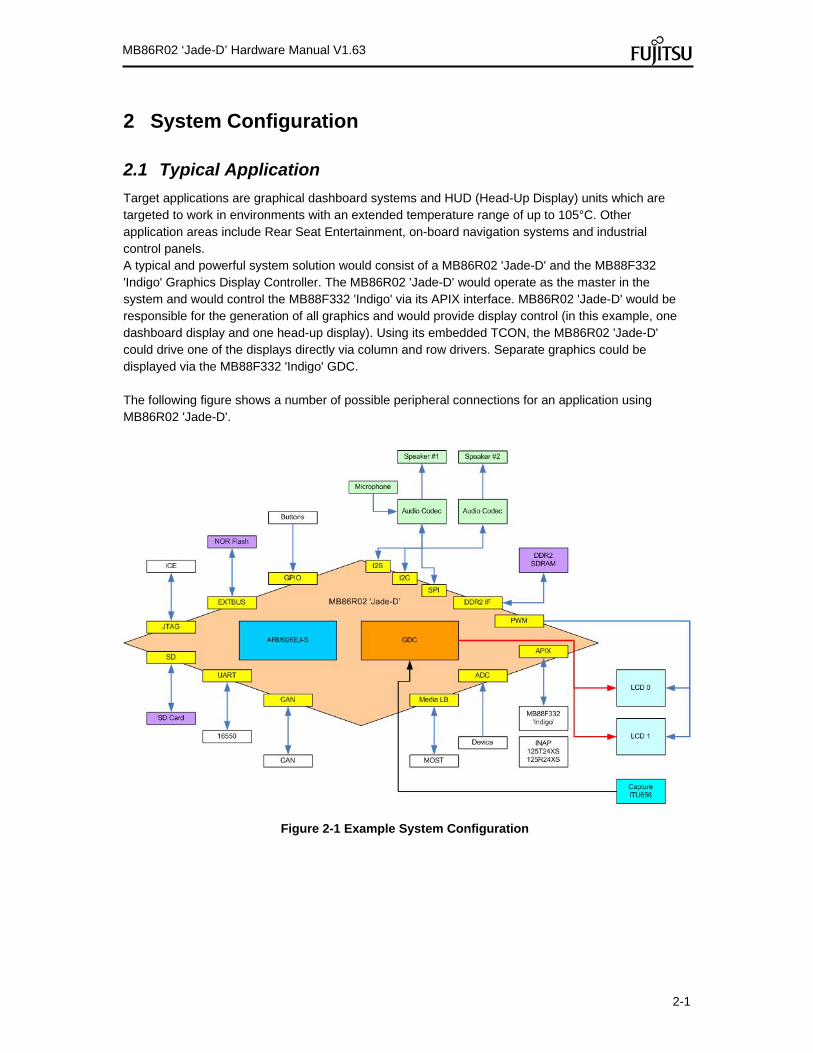
2-1
MB86R02 ‘Jade-D’ Hardware Manual V1.63
2 System Configuration
2.1 Typical Application
Target applications are graphical dashboard systems and HUD (Head-Up Display) units which are targeted to work in environments with an extended temperature range of up to 105°C. Other application areas include Rear Seat Entertainment, on-board navigation systems and industrial control panels. A typical and powerful system solution would consist of a MB86R02 'Jade-D' and the MB88F332 'Indigo' Graphics Display Controller. The MB86R02 'Jade-D' would operate as the master in the system and would control the MB88F332 'Indigo' via its APIX interface. MB86R02 'Jade-D' would be responsible for the generation of all graphics and would provide display control (in this example, one dashboard display and one head-up display). Using its embedded TCON, the MB86R02 'Jade-D' could drive one of the displays directly via column and row drivers. Separate graphics could be displayed via the MB88F332 'Indigo' GDC. The following figure shows a number of possible peripheral connections for an application using MB86R02 'Jade-D'.
Figure 2-1 Example System Configuration

3-1
MB86R02 ‘Jade-D’ Hardware Manual V1.63
3 Memory Map This chapter shows the memory map and the register map of the MB86R02 ‘Jade-D’ device.
3.1 Memory Map of LSI
Figure 3-1 shows the memory map of MB86R02 'Jade-D'. The device is booted from 0000_0000H in ROM as shown on the left side of Figure 3-1.
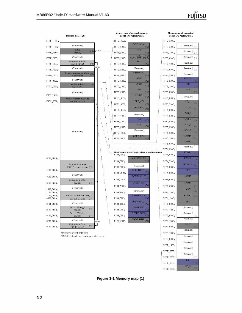
3-2
MB86R02 ‘Jade-D’ Hardware Manual V1.63
Figure 3-1 Memory map (1)
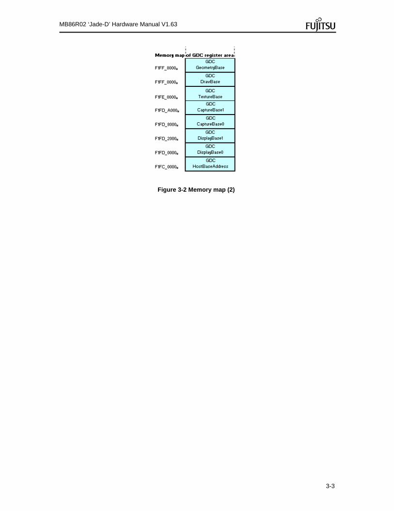
3-3
MB86R02 ‘Jade-D’ Hardware Manual V1.63
Figure 3-2 Memory map (2)

3-4
MB86R02 ‘Jade-D’ Hardware Manual V1.63
3.2 Register Access
It is necessary to access MB86R02 'Jade-D' registers with word accesses (with the exception of a few specific registers that are documented accordingly). Table 3-1 shows access data lengths for special modules.
Table 3-1 Valid access data length of register
Module Register name Valid data length
DMAC
DMACR Word (32 bit) / Half-word (16 bit) / Byte (8 bit) For byte and half-word access, use little-endian addressing1.
DMACA, DMACB, DMACSA, DMACDA
Word (32 bit)/Half-word (16 bit)/Byte (8 bit). For byte and half-word access, use little-endian addressing1.
UART RFR, TFR, DLL, DLM Word(32 bit)/Byte(8 bit) For byte access, use little-endian addressing.1
GPIO PDR0, PDR1, PDR2 Word(32 bit)/Byte(8 bit) For byte access, use little-endian addressing1.
Others All registers other than the above Word (32 bit)
1 Little-endian addressing means: - For byte access to a 32-bit register, bit[31:24] is at address offset 3, bit[23:16] at offset 2, bit[15:8] at offset 1, bit[7:0] at offset 0. - For half-word access to a 32-bit register, bit[31:16] is at address offset 2, bit[15:0] at offset 0.
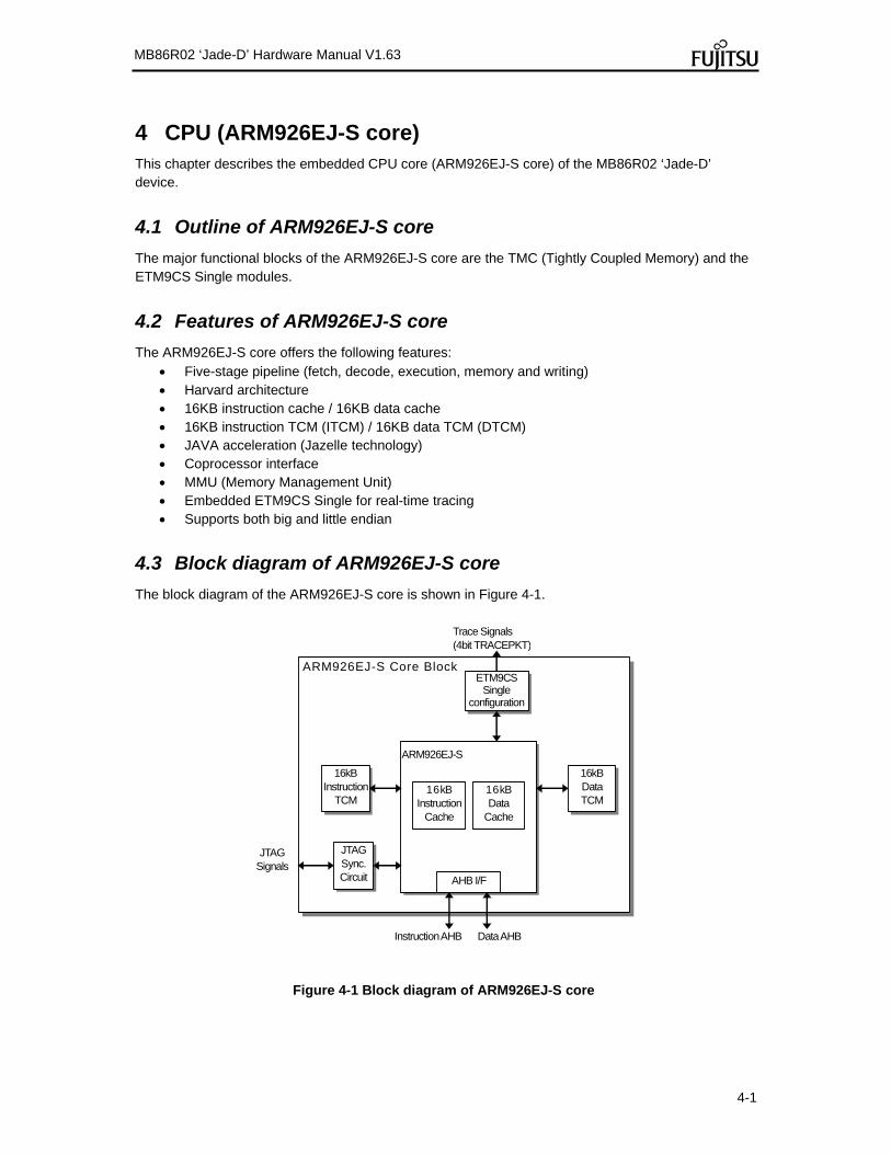
4-1
MB86R02 ‘Jade-D’ Hardware Manual V1.63
4 CPU (ARM926EJ-S core) This chapter describes the embedded CPU core (ARM926EJ-S core) of the MB86R02 ‘Jade-D’ device.
4.1 Outline of ARM926EJ-S core
The major functional blocks of the ARM926EJ-S core are the TMC (Tightly Coupled Memory) and the ETM9CS Single modules.
4.2 Features of ARM926EJ-S core
The ARM926EJ-S core offers the following features: Five-stage pipeline (fetch, decode, execution, memory and writing) Harvard architecture 16KB instruction cache / 16KB data cache 16KB instruction TCM (ITCM) / 16KB data TCM (DTCM) JAVA acceleration (Jazelle technology) Coprocessor interface MMU (Memory Management Unit) Embedded ETM9CS Single for real-time tracing Supports both big and little endian
4.3 Block diagram of ARM926EJ-S core
The block diagram of the ARM926EJ-S core is shown in Figure 4-1.
ARM926EJ-S Core Block
16kB Instruction
TCM
16kB Data TCM
JTAGSync.Circuit
ARM926EJ-S
ETM9CS Single
configuration
16kB Data
Cache
16kB Instruction
Cache
JTAG Signals
AHB I/F
Trace Signals (4bit TRACEPKT)
Instruction AHB Data AHB
Figure 4-1 Block diagram of ARM926EJ-S core

4-2
MB86R02 ‘Jade-D’ Hardware Manual V1.63
4.4 Configuration of ARM926EJ-S and ETM
The instruction and data cache are both 16KB in size. The ITCM and DTCM blocks are also 16KB in size. The embedded ETM9CS Single unit can be used for real-time tracing. Four ETMCS Single TRACEPKT ports are represented by 4 bits in the MB86R02 ‘Jade-D’ register interface. For detailed specifications of the ARM926EJ-S and ETM9CS Single modules, please refer to the documentation homepage of ARM Ltd. Various key reference documents are listed below for this purpose: ARM926EJ-S ARM926EJ-S Product Overview
ARM926EJ-S(r0p4/r0p5) Technical Reference Manual (DDI0198D) ARM9EJ-S Revision r1p2 Technical Reference Manual m,(DDI0222B) ARM926EJ-S Product Overview (DVI0035B)
The URL of the material published is as follows. http://www.arm.com/documentation/ARMProcessor_Cores/index.html ETM9CS Single relation
CoreSight ETM9 r0p0 Technical Reference Manual (DDI0315A) ETM9 Revision r2p2 Technical Reference Manual (DDI0157F) Embedded Trace Macrocell Architecture Specification (IHI0014N) CoreSight System Design Guide (DGI0012A)
The URL of the material published is as follows. http://www.arm.com/documentation/Trace_Debug/index.html
5-1
MB86R02 ‘Jade-D’ Hardware Manual V1.63
5 Clock Reset Generator (CRG) This chapter describes the functionality and operation of the Clock Reset Generator (CRG) block.
5.1 Outline
The CRG unit controls the clock and reset signals for the ARM926EJ-S, DDR2 IF, GDC, AHB, and APB modules. The APIX clock is generated separately (please refer to the APIX chapter for details).
5.2 Features
The CRG block has the following features: Clock Generator
The internal PLL clock and an external input clock (PLL by-pass mode) can be used Main PLL control
PLL oscillation control including stop PLL oscillation stabilization wait time control
SSCG control (refer to the SSCG chapter for details and a description of the registers) Clock gear control The clock frequency of the ARM core and the AXI, AHB and APB busses can be
changed separately Control of the clock (Supply/Stop) to the ARM core, AXI, AHB and APB modules
Reset Generator
Generation of an internal reset from an external reset signal Generation of a software reset Input/Output control of the XSRST signal for a JTAG ICE Generation of the XTRST (TAP controller reset) signal
Other Functions
Watchdog timer function Supports the stop mode which halts all the MB86R02 'Jade-D' clocks
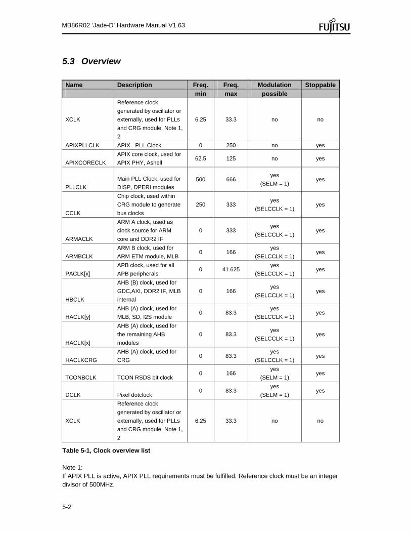
5-2
MB86R02 ‘Jade-D’ Hardware Manual V1.63
5.3 Overview
Name Description Freq. Freq. Modulation Stoppable min max possible
XCLK
Reference clock
generated by oscillator or
externally, used for PLLs
and CRG module, Note 1,
2
6.25 33.3 no no
APIXPLLCLK APIX PLL Clock 0 250 no yes
APIXCORECLK
APIX core clock, used for
APIX PHY, Ashell 62.5 125 no yes
PLLCLK
Main PLL Clock, used for
DISP, DPERI modules 500 666
yes
(SELM = 1) yes
CCLK
Chip clock, used within
CRG module to generate
bus clocks
250 333 yes
(SELCCLK = 1) yes
ARMACLK
ARM A clock, used as
clock source for ARM
core and DDR2 IF
0 333 yes
(SELCCLK = 1) yes
ARMBCLK
ARM B clock, used for
ARM ETM module, MLB 0 166
yes
(SELCCLK = 1) yes
PACLK[x]
APB clock, used for all
APB peripherals 0 41.625
yes
(SELCCLK = 1) yes
HBCLK
AHB (B) clock, used for
GDC,AXI, DDR2 IF, MLB
internal
0 166 yes
(SELCCLK = 1) yes
HACLK[y]
AHB (A) clock, used for
MLB, SD, I2S module 0 83.3
yes
(SELCCLK = 1) yes
HACLK[x]
AHB (A) clock, used for
the remaining AHB
modules
0 83.3 yes
(SELCCLK = 1) yes
HACLKCRG
AHB (A) clock, used for
CRG 0 83.3
yes
(SELCCLK = 1) yes
TCONBCLK TCON RSDS bit clock 0 166
yes
(SELM = 1) yes
DCLK Pixel dotclock 0 83.3
yes
(SELM = 1) yes
XCLK
Reference clock
generated by oscillator or
externally, used for PLLs
and CRG module, Note 1,
2
6.25 33.3 no no
Table 5-1, Clock overview list Note 1: If APIX PLL is active, APIX PLL requirements must be fulfilled. Reference clock must be an integer divisor of 500MHz.

5-3
MB86R02 ‘Jade-D’ Hardware Manual V1.63
Note 2: Configuration of PLL pre and feedback divider by CRIPM mode pins supports only a dedicated set of reference frequencies, see Table 5-3
5.4 Location in the device
CRG
APIX PHYPLL
Configuration IF
APB Bus
REFCLK
External reset from pin Internal reset
CLKX
External clock from pin
CLK
Oscillator
Clock domains
XTAL0
XTAL1
APIX Ashell
CLKY
SSCG
PLLCLK
PLLCLKMCFG
CFG from RHRegister IF
CCLK_ODISP, DPERICLKDIVCLKGATE
CFG
Figure 5-1 CRG location in the device
5.5 Operation
This section describes the operation of the CRG unit.
5.5.1 Reset Generation
Factors The following reset sources exist:
1. External reset (XRST pin input) The entire chip is initialized by a reset input from the external pin XRST.
2. Software reset (reset via register control)

5-4
MB86R02 ‘Jade-D’ Hardware Manual V1.63
A software reset occurs by writing "1" to the SWRSTREQ bit of the reset/standby control register (CRSR). It does not change the state to PLL oscillation stabilization even if the PLLBYPASS bit of the PLL control register (CRPR) is "0" (setting that uses PLL clock.) In addition, this reset does not change the CRG module register, VINITHI control register of remap/boot controller (RBC) or the INITRAM control register. The clock source of the software reset is time based on the timer’s count value. It is cleared when a software reset is asserted. This software reset generates the internal signal, which does not reset as CRSTn.
3. XSRST (reset request from a debugging tool) This signal is a reset request from a debugging tool (e.g. MultiICE) and an internal reset request can be transmitted by the tool through the XSRST pin. This module recognizes the reset signal as the same reset request as that of an external reset.
4. XTRST (built-in ICE macro reset request from a debugging tool) This signal is a built-in ICE macro reset request from a debugging tool (e.g. MultiICE) and the reset signal requests a reset from the embedded ICE macro in the ARM9 core. Although the reset signal is asserted, other peripherals are not initialized. The embedded ETM9CS Single trace cell is also reset by this signal.

5-5
MB86R02 ‘Jade-D’ Hardware Manual V1.63
5. Watchdog reset The watchdog timer starts when the WDTSET/WDTCLR bits of the watchdog timer control register (CRWR) are set to "1" after an external reset. Writing "1" to the WDTSET/WDTCLR bits a second time or at a later point in time clears the timer. The clock source of the watchdog timer is the count value of the time based timer. A clear operation of the time based timer effects the watchdog timer’s count value. When the timer is cleared, the watchdog timer is also cleared.
Selected time base timer bit
WDTCLR (max)
WDTCLR (min)
Watchdog reset request
Tclk x 2n
Tclk x 2(n+1)
Figure 5-2 Watchdog reset timing
As shown in Figure 5-2, a watchdog reset occurs after the second falling edge of the selected time-based timer bit. In ARM9 debug mode (DBGACK = 1)during PLL oscillation stabilization waiting time, CRG clears the watchdog timer. In addition, it monitors the standby mode of the ARM9 core and clears the watchdog timer automatically in standby mode (standby mode = 1.)
Reset output signal The reset signal output by the reset generator is as follows depending on the reset source:
HRESETn (AHB/APB bus reset) This internal reset signal initializes the ARM9 core and AHB/APB peripherals and is output by an external reset, software reset or XSRST reset.
XSRST (reset monitoring) This signal functions as a report to the external circuit of ARM’s internal reset source. This signal is asserted in the same way as the HRESETn signal.
Internal XTRST (built-in ICE macro reset) This signal initializes the embedded macro of the ARM9 core. The macro must be reset at power-on so that this signal is output by an external reset or an external XTRST reset.
CRSTn (internal reset) This signal is output by an external reset or an XSRST reset.

5-6
MB86R02 ‘Jade-D’ Hardware Manual V1.63
The following table shows the correlation between the reset sources and reset output signals.
Table 5-2 Correlation between reset sources and reset output signals
Reset output Reset source
External reset Software reset Input XSRST XTRST Watchdog reset
HRESETn Asserted Asserted Asserted Not asserted Asserted
Output XSRST Asserted Asserted Not asserted Not asserted Asserted
Internal XTRST Asserted Not asserted Not asserted Asserted Not asserted
CRSTn Asserted Not asserted Asserted Not asserted Asserted

5-7
MB86R02 ‘Jade-D’ Hardware Manual V1.63
5.5.2 Clock Generation
The MB86R02 'Jade-D' device has several clock domains. The pixel clock domain operates with a modulated clock in order to reduce electromagnetic interference in the display controller and display output modules. A second domain operates with a non-modulated clock in order to communicate with the automotive network. Each clock can be seperately disabled (see registers CRHA, CRHB, CRPA, CRPB, CRAM). Please be aware that each clock is enabled after a reset. For power saving reasons, clocks for non-active modules should be disabled.
Figure 5-3 Overview of Clock Structure PLL's

5-8
MB86R02 ‘Jade-D’ Hardware Manual V1.63
DIV1/LX
GateCCLK ARMA_OUsed for ARM & DDR IF
DIV1/LX
Gate
STOP | ARMAGATE[0]ARMADM[2:0]
ARMB_O(ETMclock)
STOP | ARMBGATE[0]ARMBDM[2:0]
Figure 5-4 Clock Structure, ARM clocks For each divider Lx is 1, 2, 4, 8, 16
Figure 5-5 Clock structure, DCLK
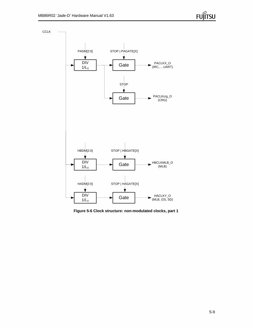
5-9
MB86R02 ‘Jade-D’ Hardware Manual V1.63
DIV1/LX
Gate PACLKX_O(IRC,….UART)
CCLK
Gate
STOP | PAGATE[X]PADM[2:0]
PACLKcrg_O(CRG)
STOP
Gate HBCLKMLB_O(MLB)
DIV1/LX
Gate HACLKY_O(MLB, I2S, SD)
DIV1/LX
HBDM[2:0]
HADM[2:0]
STOP | HBGATE[X]
STOP | HAGATE[X]
Figure 5-6 Clock structure: non-modulated clocks, part 1
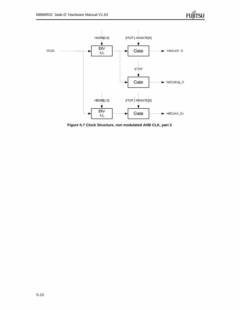
5-10
MB86R02 ‘Jade-D’ Hardware Manual V1.63
Figure 5-7 Clock Structure, non modulated AHB CLK, part 2

5-11
MB86R02 ‘Jade-D’ Hardware Manual V1.63
PLL Control
Oscillation stabilization waiting period The clock transmission source for the oscillation stabilization waiting period is the count value of the time-based timer. Clearing the time-based timer effects its count value. If this module's state is changed to PLL oscillation stabilization waiting state as shown below, the time-based timer is cleared.
(1) External reset is asserted ("M" and "m" of LUWMODE in the 5.1.2 PLL control
register (CRPR))
PLL oscillation stabilization waiting
ERSTn
PLL reset CLK
1/M PLL clock
CCLK
HRESETn
PLLREADY
PLLBYPASS
6 CLK cycles
a) External reset deasserted (XRST) b) ERSTn reset (CRG internal signal) c) PLL reset deasserted d) PLL ready e) HRESETn deasserted
a) b) c) d) e)
XRST
(m2 + 2) CLKcycles 21 or more CCLK cycles
Figure 5-8 PLL oscillation stabilization waiting state after external reset
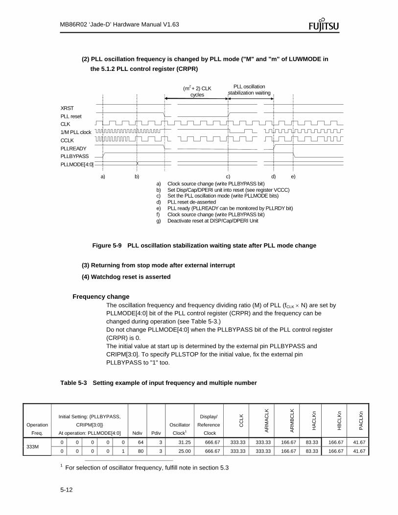
5-12
MB86R02 ‘Jade-D’ Hardware Manual V1.63
(2) PLL oscillation frequency is changed by PLL mode ("M" and "m" of LUWMODE in
the 5.1.2 PLL control register (CRPR)
XRST
PLL reset
CLK
1/M PLL clock
CCLK
PLLREADY
PLLBYPASS
PLLMODE[4:0]
PLL oscillation stabilization waiting
a) Clock source change (write PLLBYPASS bit) b) Set Disp/Cap/DPERI unit into reset (see register VCCC) c) Set the PLL oscillation mode (write PLLMODE bits) d) PLL reset de-asserted e) PLL ready (PLLREADY can be monitored by PLLRDY bit) f) Clock source change (write PLLBYPASS bit) g) Deactivate reset at DISP/Cap/DPERI Unit
c) d) e) b)
a)
(m2 + 2) CLK cycles
Figure 5-9 PLL oscillation stabilization waiting state after PLL mode change
(3) Returning from stop mode after external interrupt
(4) Watchdog reset is asserted
Frequency change The oscillation frequency and frequency dividing ratio (M) of PLL (fCLK N) are set by PLLMODE[4:0] bit of the PLL control register (CRPR) and the frequency can be changed during operation (see Table 5-3.) Do not change PLLMODE[4:0] when the PLLBYPASS bit of the PLL control register (CRPR) is 0. The initial value at start up is determined by the external pin PLLBYPASS and CRIPM[3:0]. To specify PLLSTOP for the initial value, fix the external pin PLLBYPASS to "1" too.
Table 5-3 Setting example of input frequency and multiple number
Operation
Freq.
Initial Setting: PLLBYPASS,
CRIPM[3:0]
At operation: PLLMODE[4:0] Ndiv Pdiv
Oscillator
Clock1
Display/
Reference
Clock
CC
LK
AR
MA
CL
K
AR
MB
CL
K
HA
CL
Kn
HB
CL
Kn
PA
CL
Kn
333M 0 0 0 0 0 64 3 31.25 666.67 333.33 333.33 166.67 83.33 166.67 41.67
0 0 0 0 1 80 3 25.00 666.67 333.33 333.33 166.67 83.33 166.67 41.67
1 For selection of oscillator frequency, fulfill note in section 5.3

5-13
MB86R02 ‘Jade-D’ Hardware Manual V1.63
0 0 0 1 0 32 1 20.8333 666.67 333.33 333.33 166.67 83.33 166.67 41.67
0 0 0 1 1 33 1 20.00 660.00 330.00 330.00 165.00 82.50 165.00 41.25
320M
0 0 1 0 0 61 3 31.25 635.42 317.71 317.71 158.85 79.43 158.85 39.71
0 0 1 0 1 51 2 25.00 637.50 318.75 318.75 159.38 79.69 159.38 39.84
0 0 1 1 0 92 3 20.8333 638.89 319.44 319.44 159.72 79.86 159.72 39.93
0 0 0 1 0 32 1 20.00 640.00 320.00 320.00 160.00 80.00 160.00 40.00
266M
0 1 0 0 0 17 1 31.25 531.25 265.63 265.63 132.81 66.41 132.81 33.20
0 0 0 0 0 64 3 25.00 533.33 266.67 266.67 133.33 66.67 133.33 33.33
0 0 1 0 1 51 2 20.8333 531.25 265.62 265.62 132.81 66.41 132.81 33.20
0 0 0 0 1 80 3 20.00 533.33 266.67 266.67 133.33 66.67 133.33 33.33
1 1 1 1 1 PLLSTOP
PLLBYPASS The main clock (CCLK) of the CRG module can be dynamically switched between the PLL clock and an external input clock (CLK) using PLLBYPASS bit of the PLL control register (CRPR).
CLK
1/M PLL clock
CCLK
PLLREADY
PLLBYPASS
a) a) Clock source change (write PLLBYPASS bit (write 0))
b) Clock source change (write PLLBYPASS bit (write 1))
b)
Clock switching Clock switching
Figure 5-10 Clock switching between the PLL clock / external clock
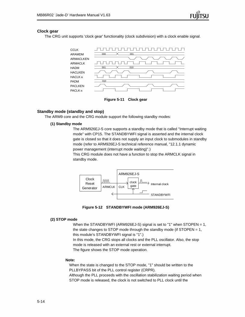
5-14
MB86R02 ‘Jade-D’ Hardware Manual V1.63
Clock gear The CRG unit supports 'clock gear' functionality (clock subdivision) with a clock enable signal.
CCLK
ARAMDM
ARMACLKEN
ARMACLK
HADM
HACLKEN
HACLK
000
001
001
010
PADM
PACLKEN
PACLK
010
Figure 5-11 Clock gear
Standby mode (standby and stop) The ARM9 core and the CRG module support the following standby modes:
(1) Standby mode The ARM926EJ-S core supports a standby mode that is called "Interrupt waiting mode" with CP15. The STANDBYWFI signal is asserted and the internal clock gate is closed so that it does not supply an input clock to submodules in standby mode (refer to ARM926EJ-S technical reference manual, "12.1.1 dynamic power management (interrupt mode waiting)".) This CRG module does not have a function to stop the ARMCLK signal in standby mode.
ARMCLK
Clock Reset
Generator
ARM926EJ-S
CLK
clockgate
STANDBYWFI
Internal clock
Figure 5-12 STANDBYWFI mode (ARM926EJ-S)
(2) STOP mode When the STANDBYWFI (ARM926EJ-S) signal is set to "1" when STOPEN = 1, the state changes to STOP mode through the standby mode (if STOPEN = 1, this module’s STANDBYWFI signal is "1".) In this mode, the CRG stops all clocks and the PLL oscillator. Also, the stop mode is released with an external rest or external interrupt. The figure shows the STOP mode operation.
Note:
When the state is changed to the STOP mode, "1" should be written to the PLLBYPASS bit of the PLL control register (CRPR). Although the PLL proceeds with the oscillation stabilization waiting period when STOP mode is released, the clock is not switched to PLL clock until the

5-15
MB86R02 ‘Jade-D’ Hardware Manual V1.63
PLLBYPASS bit becomes "0". Also, the PLL oscillation stabilization waiting state is skipped if PLLMODE[4:0] is 5’b11111.
CLK
STOP mode
STOPEN STANDBYWFI PACLK0_STP STOP WAKEUP CCLK ARMA(B)CLK HACLK PACLK PLLBYPASS PLLRDY PLL clock PLL reset
PLL oscillation stabilization waiting
* STOP = CLK clock is able to stop while the value is "1”
Figure 5-13 Stop mode

5-16
MB86R02 ‘Jade-D’ Hardware Manual V1.63
5.6 Registers
This section describes the registers of the CRG unit.
5.1.1. Register list
Table 5-4 lists the CRG registers.
Table 5-4 CRG register list
Address Register name
Abbreviation
Explanation Base Offset
FFFE_7000H + 00H PLL control register CRPR To control PLL
+ 04H (Reserved) – Reserved area, access prohibited
+ 08H Watchdog timer control register CRWR To control watchdog timer
+ 0CH Reset/Standby control register CRSR To control reset/standby
+ 10H Clock frequency dividing control register A
CRDA To control clock divider
+ 14H Clock frequency dividing control register B
CRDB To control clock divider
+ 18H AHB(A) bus clock gate control register
CRHA To control clock gate of AHB(A) bus
+ 1CH APB(A) bus clock gate control register
CRPA To control clock gate of APB(A) bus
+ 20H APB(B) bus clock gate control register
CRPB To control clock gate of APB(B) bus
+ 24H AHB(B) bus clock gate control register
CRHB To control clock gate of AHB(B) bus
+ 28H ARM core clock gate control register
CRAM To control clock gate of ARM core
+ 2CH DPERI02 clock gate control register
CRDP0 TO control clock gate of DPERI0
+ 30H DPERI13 clock gate control register
CRDP1 TO control clock gate of DPERI1
+ 34H Clock Selection Control register (Reserved)
CSEL To control clock mutliplexers
+ 35H – + 7FH
(Reserved) – Reserved area, access prohibited
+ 80H – + EFH
SSCG registers – see chapter SSCG (Spread Spectrum Clock Generation)
+ F0H – + FFH
(Reserved) – Reserved area, access prohibited
Note 2DPERI0 means the display peripherals of pixel output pipeline 0. These are color lookup table CLUT,
dither module DITH, signature module SIG and timing controller TCON
3 DPERI1 means the display peripherals of pixel output pipeline 1. These are color lookup table
CLUT, dither module DITH and signature module SIG

5-17
MB86R02 ‘Jade-D’ Hardware Manual V1.63
Description format of register Following format is used for description of register’s each bit in "5.1.2 PLL control register (CRPR)" to "5.1.11 ARM core clock gate control register (CRAM)".
Address Base address + Offset
Bit 31 30 29 28 27 26 25 24 23 22 21 20 19 18 17 16 Name R/W
Initial value Bit 15 14 13 12 11 10 9 8 7 6 5 4 3 2 1 0
Name R/W
Initial value
Meaning of item and sign Address
Address (base address + offset address) of the register Bit
Bit number of the register Name
Bit field name of the register R/W
Attribution of read/write of each bit field R0:Read value is always "0" R1: Read value is always "1" W0: Write value is always "0", and write access of "1" is ignored W1: Write value is always "1", and write access of "0" is ignored R: Read W: Write Initial value
Each bit field’s value after reset 0: Value is "0" 1: Value is "1" X: Value is undefined
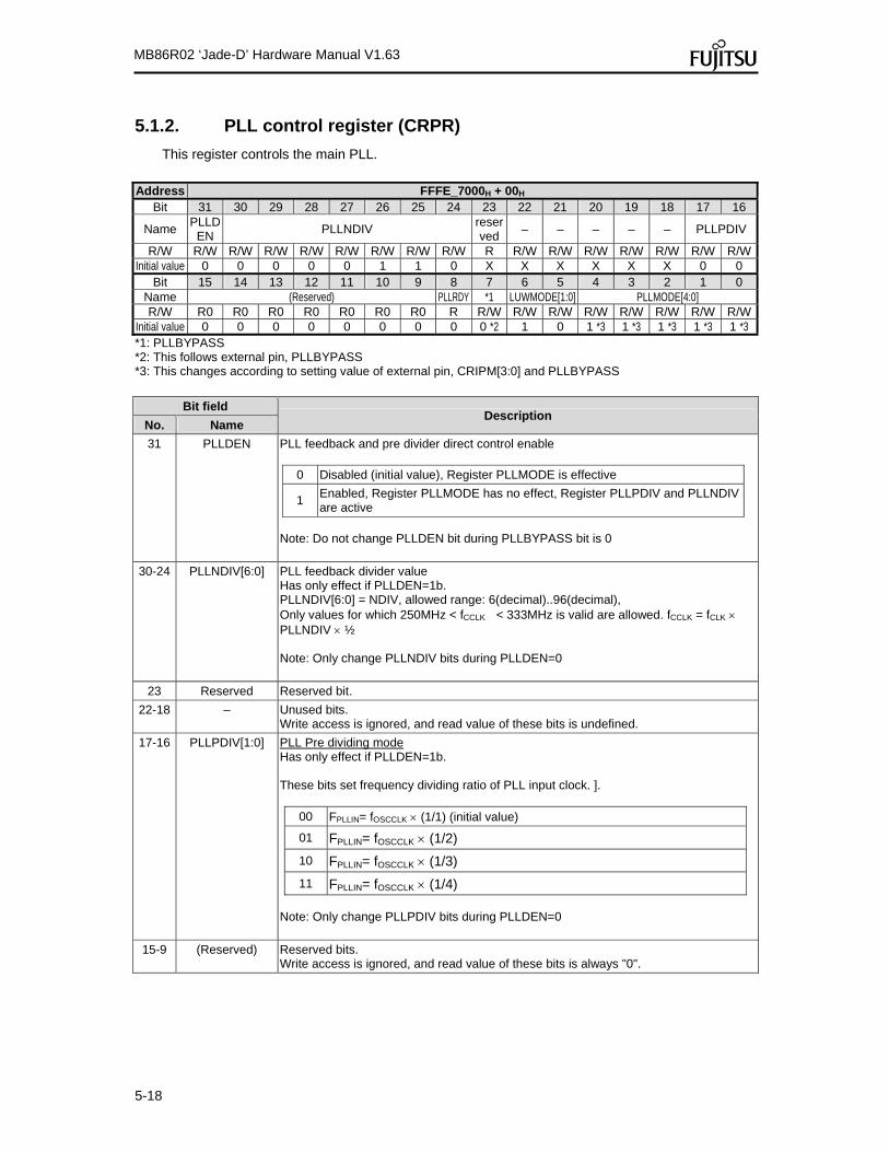
5-18
MB86R02 ‘Jade-D’ Hardware Manual V1.63
5.1.2. PLL control register (CRPR)
This register controls the main PLL.
Address FFFE_7000H + 00H Bit 31 30 29 28 27 26 25 24 23 22 21 20 19 18 17 16
Name PLLD
EN PLLNDIV
reserved
– – – – – PLLPDIV
R/W R/W R/W R/W R/W R/W R/W R/W R/W R R/W R/W R/W R/W R/W R/W R/WInitial value 0 0 0 0 0 1 1 0 X X X X X X 0 0
Bit 15 14 13 12 11 10 9 8 7 6 5 4 3 2 1 0 Name (Reserved) PLLRDY *1 LUWMODE[1:0] PLLMODE[4:0] R/W R0 R0 R0 R0 R0 R0 R0 R R/W R/W R/W R/W R/W R/W R/W R/W
Initial value 0 0 0 0 0 0 0 0 0 *2 1 0 1 *3 1 *3 1 *3 1 *3 1 *3 *1: PLLBYPASS *2: This follows external pin, PLLBYPASS *3: This changes according to setting value of external pin, CRIPM[3:0] and PLLBYPASS
Bit field
Description No. Name
31 PLLDEN PLL feedback and pre divider direct control enable
0 Disabled (initial value), Register PLLMODE is effective
1 Enabled, Register PLLMODE has no effect, Register PLLPDIV and PLLNDIV are active
Note: Do not change PLLDEN bit during PLLBYPASS bit is 0
30-24 PLLNDIV[6:0] PLL feedback divider value Has only effect if PLLDEN=1b. PLLNDIV[6:0] = NDIV, allowed range: 6(decimal)..96(decimal), Only values for which 250MHz < fCCLK < 333MHz is valid are allowed. fCCLK = fCLK PLLNDIV ½ Note: Only change PLLNDIV bits during PLLDEN=0
23 Reserved Reserved bit.
22-18 – Unused bits. Write access is ignored, and read value of these bits is undefined.
17-16 PLLPDIV[1:0] PLL Pre dividing mode Has only effect if PLLDEN=1b. These bits set frequency dividing ratio of PLL input clock. ].
00 FPLLIN= fOSCCLK (1/1) (initial value)
01 FPLLIN= fOSCCLK (1/2)
10 FPLLIN= fOSCCLK (1/3)
11 FPLLIN= fOSCCLK (1/4) Note: Only change PLLPDIV bits during PLLDEN=0
15-9 (Reserved) Reserved bits. Write access is ignored, and read value of these bits is always "0".

5-19
MB86R02 ‘Jade-D’ Hardware Manual V1.63
Bit field Description
No. Name
8 PLLRDY PLLREADY monitoring This bit monitors internal signal, PLLREADY with external pin CLK clock. The PLLREADY signal shows overflow of the value selected at LUMMODE[1:0] bit by the timer which calculates PLL oscillation stabilization waiting time.
0 PLLREADY signal is "low" (initial value)
1 PLLREADY signal is "high" Write access to this bit is ignored.
7 PLLBYPASS PLL bypass mode This bit bypasses PLL.
0 PLL clock is used.
1 PLL is bypassed Note: Do not change PLLBYPASS bit and PLLMODE[4:0] at the same time since clock
switch of both external pin CLK and PLL clocks needs to be changed. If they are changed at the same time, CRG detects PLL oscillation frequency change and state becomes PLL oscillation stabilization waiting before PLL bypass mode.
Reference: The initial value of this bit is settable with setting external pin, PLLBYPASS.
6-5 LUWMODE[1:0] PLL locked waiting mode These bits are used to set PLL oscillation stabilization wait time.
00 TCLK (2n0 - 2m + 1)
01 TCLK (2n1 - 2m + 1)
10 TCLK (2n2 - 2m + 1) (initial value)
11 TCLK (2n3 - 2m + 1)
TCLK: Cycle time of CLK reference clock n0 = 11 n1 = 12 n2 = 13 n3 = 14 m = 8 The wait time depends on CLK cycle time and PLL lock-up time, moreover it does not need to be changed from the initial value.

5-20
MB86R02 ‘Jade-D’ Hardware Manual V1.63
Bit field Description
No. Name
4-0 PLLMODE[4:0] PLL oscillation mode These bits are used to set PLL oscillation mode. Initial value of PLLMODE[4:0] bit changes according to the setting of external pin, CRIPM[3:0]. Initial value of these bits is PLLMODE[4:0] = "0", CRIPM[3], CRIPM[2], CRIPM[1], CRIPM[0].
00000 fCCLK = fCLK 10.67 (64 x 1/3 1/2)
00001 fCCLK = fCLK 13.33 (80 x 1/3 1/2)
00010 fCCLK = fCLK 16.00 (32 1/2)
00011 fCCLK = fCLK 16.50 (33 1/2)
00100 fCCLK = fCLK 10.17 (61 x 1/3 1/2)
00101 fCCLK = fCLK 12.75 (51 x 1/2 1/2)
00110 fCCLK = fCLK 15.33 (92 x 1/3 1/2)
00111 reserved
01000 fCCLK = fCLK 8.5 (17 1/2)
01001 reserved
01010 reserved
01011 reserved
11111 PLL stops
Others Reserved (setting prohibited)
fCCLK : Clock frequency of CCLK fCLK : Clock frequency of external pin CLK
Note: Do not change PLLMODE[4:0] when PLLBYPASS bit is 0.

5-21
MB86R02 ‘Jade-D’ Hardware Manual V1.63
5.1.3. Watchdog timer control register (CRWR)
This register controls watchdog timer.
Address FFFE_7000H + 08H Bit 31 30 29 28 27 26 25 24 23 22 21 20 19 18 17 16
Name – – – – – – – – – – – – – – – – R/W R/W R/W R/W R/W R/W R/W R/W R/W R/W R/W R/W R/W R/W R/W R/W R/W
Initial value X X X X X X X X X X X X X X X X Bit 15 14 13 12 11 10 9 8 7 6 5 4 3 2 1 0
Name (Reserved) ERS
T (Reserved) TBR WDRST
WDTSET/WDTCL
R WDTMODE[1:0]
R/W R0 R0 R0 R0 R0 R0 R0 R0 R/W0 R0 R0/W0
* R/W1 R/W0 R/W1 R/W R/W
Initial value 0 0 0 0 0 0 0 0 1 0 0 0 X 0 0 0 *: Do not set "1" to bit 5
Bit field
Description No. Name
31-16 – Unused bits. Write access is ignored, and read value of these bits is undefined.
15-8 (Reserved) Reserved bits. Write access is ignored, and read value of these bits is always "0".
7 ERST Internal reset of ERSTn monitoring This bit monitors internal signal of ERSTn.
0 ERSTn is asserted
1 ERSTn is cancelled (initial value) The initial value of this bit is set to 1 by falling edge of ERSTn., and writing "1" is ignored. This bit is set by ERSTn.
6 (Reserved) Reserved bits. Write access is ignored, and read value of these bits is always "0".
5 (Reserved) Reserved bit, always write 0. Read value of this bit is always "0".
4 TBR Time based timer reset request This bit resets the time based timer, and its reset signal is asserted during 1 cycle of APB clock.
0 Time based timer is not reset (initial value)
1 Reset the time based timer Writing 0 is ignored.
3 WDRST Watchdog reset monitoring This bit monitors watchdog reset.
0 Watchdog reset is not asserted
1 Watchdog reset is asserted The initial value of this bit is undefined, and writing 1 is ignored. When watchdog is reset, this bit is set to "1".

5-22
MB86R02 ‘Jade-D’ Hardware Manual V1.63
Bit field Description
No. Name
2 WDTSET /WDTCLR
Setting and clear of watchdog timer This bit sets and clears watchdog timer which starts count at writing "1" and clears at writing "1" from the second time.
0 The watchdog timer is not set (Initial value)
1 First time: The watchdog timer starts Second time or later: The watchdog timer is cleared
Writing 0 is ignored.
1-0 WDTMODE[1:0] These bits set timing to clear watchdog timer. Watchdog reset occurs at following period when "1" is written to WDTSET/WDTCLR bits at the end.
00 TCLK 2n0 ~ TCLK 2(n0 + 1) (initial value)
01 TCLK 2n1 ~ TCLK 2(n1 + 1)
10 TCLK 2n2 ~ TCLK 2(n2 + 1)
11 TCLK 2n3 ~ TCLK 2(n3 + 1)
TCLK: Cycle time of external pin CLK n0 = 9 n1 = 12 n2 = 14 n3 = 16 Select the bit that is corresponded to the system.

5-23
MB86R02 ‘Jade-D’ Hardware Manual V1.63
5.1.4. Reset/Standby control register (CRSR)
This register controls reset and standby.
Address FFFE_7000H + 0CH Bit 31 30 29 28 27 26 25 24 23 22 21 20 19 18 17 16
Name – – – – – – – – – – – – – – – – R/W R/W R/W R/W R/W R/W R/W R/W R/W R/W R/W R/W R/W R/W R/W R/W R/W
Initial value X X X X X X X X X X X X X X X X Bit 15 14 13 12 11 10 9 8 7 6 5 4 3 2 1 0
Name (Reserved) STOPEN (Reserved) Reserved SRST SWRST SWRST
REQ SWRMODE
R/W R0 R0 R0 R0 R0 R0 R0 R0 R/W R0 R0 R/W0 R/W0 R/W0 R/W1 R/WInitial value 0 0 0 0 0 0 0 0 0 0 0 0 X X 0 0
Bit field Description
No. Name
31-16 – Unused bits. Write access is ignored, and read value of these bits is undefined.
15-8 (Reserved) Reserved bits. Write access is ignored, and read value of these bits is always "0".
7 STOPEN Stop mode enable This bit stops all bus clock operations in the standby mode.
0 Bus clock operation in the standby mode does not stop (initial value)
1 All bus clock operations in the standby mode are stopped Note: clocks are not stopped immediately Note: When changing state to stop mode, write "1" to PLLBYPASS bit of CRPR.
6-5 (Reserved) Reserved bits. Write access is ignored, and read value of these bits is always "0".
4 (Reserved) Reserved bit. Always write "0" to write access.
3 SRST nSRST monitoring This bit monitors nSRST reset from ICE.
0 nSRST is not asserted
1 nSRST is asserted Initial value of this bit is undefined, and writing "0" is ignored. When nSRST occurs, this bit is set to "1".
2 SWRST Software reset monitoring This bit monitors software reset.
0 Software reset is not asserted
1 Software reset is asserted Initial value of this bit is undefined, and writing "0" is ignored. When software reset occurs, this bit is set to "1".
1 SWRSTREQ Software reset request This bit asserts software reset.
0 Software reset is not requested (initial value)
1 Software reset is requested Writing 0 is ignored, and this bit is cleared with reset signal.

5-24
MB86R02 ‘Jade-D’ Hardware Manual V1.63
Bit field Description
No. Name
0 SWRMODE Pulse width mode of software reset This bit sets pulse width of software reset.
0 TCLK (2n0+3) + TCCLK 7 (initial value)
1 TCLK (2n1+3) + TCCLK 7
TCLK: Cycle time of reference clock CLK TCCLK: Cycle time of internal signal CCLK n0 = 7 n1 = 12 Pulse width of software reset depends on the CLK cycle time and internal operation frequency setting. Select the bit that is corresponded to the system.

5-25
MB86R02 ‘Jade-D’ Hardware Manual V1.63
5.1.5. Clock divider control register A (CRDA)
This register controls clock divider.
Address FFFE_7000H + 10H Bit 31 30 29 28 27 26 25 24 23 22 21 20 19 18 17 16
Name – – – – – – – – – – – – – – – – R/W R/W R/W R/W R/W R/W R/W R/W R/W R/W R/W R/W R/W R/W R/W R/W R/W
Initial value X X X X X X X X X X X X X X X X Bit 15 14 13 12 11 10 9 8 7 6 5 4 3 2 1 0
Name (Reserved) ARMBDM[2:0] ARMADM[2:0] reserved[2:0] PADM[2:0] HADM[2:0] R/W R0 R/W R/W R/W R/W R/W R/W R/W R/W R/W R/W R/W R/W R/W R/W R/W
Initial value 0 0 0 1 0 0 0 0 1 1 0 1 1 0 1 0
Bit field
Description No. Name
31-16 – Unused bits. Write access is ignored, and read value of these bits is undefined.
15 (Reserved) Reserved bit. Write access is ignored, and read value of these bits is always "0".
14-12 ARMBDM[2:0] ARMBCLK frequency dividing mode These bits set frequency dividing ratio of ARMBCLK.
000 fARMBCLK = fCCLK (1/1)
001 fARMBCLK = fCCLK (1/2) (initial value)
010 fARMBCLK = fCCLK (1/4)
011 fARMBCLK = fCCLK (1/8)
100 fARMBCLK = fCCLK (1/16)
Others Reserved (setting prohibited)
fARMBCLK : Clock frequency of ARMBCLK fCCLK : Clock frequency of CCLK
11-9 ARMADM[2:0] ARMACLK dividing mode These bits set frequency dividing ratio of ARMACLK.
000 fARMACLK = fCCLK (1/1) (initial value)
001 fARMACLK = fCCLK (1/2)
010 fARMACLK = fCCLK (1/4)
011 fARMACLK = fCCLK (1/8)
100 fARMACLK = fCCLK (1/16)
Others Reserved (setting prohibited)
fARMACLK : Clock frequency of ARMACLK fCCLK : Clock frequency of CCLK
8-6 Reserved

5-26
MB86R02 ‘Jade-D’ Hardware Manual V1.63
Bit field Description
No. Name
5-3 PADM[2:0] PACLK frequency dividing mode These bits set frequency dividing ratio of PACLK.
000 fPACLK = fCCLK (1/1)
001 fPACLK = fCCLK (1/2)
010 fPACLK = fCCLK (1/4)
011 fPACLK = fCCLK (1/8) (initial value)
100 fPACLK = fCCLK (1/16)
Others Reserved (setting prohibited)
fPACLK : Clock frequency of PACLK fCCLK : Clock frequency of CCLK
2-0 HADM[2:0] HACLK frequency dividing mode These bits set frequency dividing ratio of HACLK.
000 fHACLK = fCCLK (1/1)
001 fHACLK = fCCLK (1/2)
010 fHACLK = fCCLK (1/4) (initial value)
011 fHACLK = fCCLK (1/8)
100 fHACLK = fCCLK (1/16)
Others Reserved (setting prohibited)
fHACLK : Clock frequency of HACLK fCCLK : Clock frequency of CCLK
Note:
ARMACLK must not be slower than HACLK; moreover, HACLK may not be slower than PACLK.
fARMCLK >= fHACLK >= fPACLK

5-27
MB86R02 ‘Jade-D’ Hardware Manual V1.63
5.1.6. Clock divider control register B (CRDB)
This register controls clock divider.
Address FFFE_7000H + 14H Bit 31 30 29 28 27 26 25 24 23 22 21 20 19 18 17 16
Name – – – – – – – – – – – – – – – – R/W R/W R/W R/W R/W R/W R/W R/W R/W R/W R/W R/W R/W R/W R/W R/W R/W
Initial value X X X X X X X X X X X X X X X X Bit 15 14 13 12 11 10 9 8 7 6 5 4 3 2 1 0
Name (Reserved) HBDM[2:0] R/W R0 R0 R0 R0 R0 R0 R0 R0 R0 R0 R0 R0 R0 R/W R/W R/W
Initial value 0 0 0 0 0 0 0 0 0 0 0 0 0 0 0 1
Bit field
Description No. Name
31-16 – Unused bits. Write access is ignored, and read value of these bits is undefined.
15-3 (Reserved) Reserved bits. Write access is ignored, and read value of these bits is always "0".
2-0 HBDM[2:0] HBCLK frequency dividing mode These bits set frequency dividing ratio of HBCLK.
HBDM[2:0] Frequency dividing ratio of HBCLK
000 fHBCLK = fCCLK (1/1)
001 fHBCLK = fCCLK (1/2) (initial value)
010 fHBCLK = fCCLK (1/4)
011 fHBCLK = fCCLK (1/8)
100 fHBCLK = fCCLK (1/16)
Others Reserved (setting prohibited)
fHBCLK : Clock frequency of HBCLK fCCLK : Clock frequency of CCLK

5-28
MB86R02 ‘Jade-D’ Hardware Manual V1.63
5.1.7. AHB (A) bus clock gate control register (CRHA)
This register controls clock gate of AHB (A) bus.
Address FFFE_7000H + 18H Bit 31 30 29 28 27 26 25 24 23 22 21 20 19 18 17 16
Name – – – – – – – – HAGATE[23:16] R/W R/W R/W R/W R/W R/W R/W R/W R/W R/W R/W R/W R/W R/W R/W R/W R/W
Initial value X X X X X X X X 1 1 1 1 1 1 1 1 Bit 15 14 13 12 11 10 9 8 7 6 5 4 3 2 1 0
Name HAGATE[15:0] R/W R/W R/W R/W R/W R/W R/W R/W R/W R/W R/W R/W R/W R/W R/W R/W R/W
Initial value 1 1 1 1 1 1 1 1 1 1 1 1 1 1 1 1
Bit field
Description No. Name
31-24 – Unused bits. Write access is ignored, and read value of these bits is undefined.
23-0 HAGATE[23:0] HACLK clock gate control These bits control HACLK clock gate.
HAGATE[n] Description
0 HACLKn stops
1 HACLKn does not stop (initial value) HACLK0: AHB1, AHB2, APBBRG0, APBBRG1, APBBRG2, AHB2AHB HACLK1: External bus I/F, CCPB HACLK2: SRAM HACLK3: HDMAC HACLK4: (Reserved) HACLK5: Boot ROM HACLK6: (Reserved) HACLK7: I2S HACLK8: (Reserved) HACLK9: (Reserved) HACLK10: SD I/F HACLK11: (Reserved) HACLK12: MLB HACLK13: GDC HACLK14: (Reserved) HACLK15: DDR2 controller HACLK16: RH TX0 HACLK17: RH TX1 HACLK18: RH RX0 HACLK19: RH RX1 HACLK20: RLD HACLK21: DPERI0 HACLK22: DPERI1 HACLK23: SPI-HOST

5-29
MB86R02 ‘Jade-D’ Hardware Manual V1.63
5.1.8. APB (A) bus clock gate control register (CRPA)
This register controls clock gate of APB (A) bus.
Address FFFE_7000H + 1CH Bit 31 30 29 28 27 26 25 24 23 22 21 20 19 18 17 16
Name – – – – – – – – – – – – – – – – R/W R/W R/W R/W R/W R/W R/W R/W R/W R/W R/W R/W R/W R/W R/W R/W R/W
Initial value X X X X X X X X X X X X X X X X Bit 15 14 13 12 11 10 9 8 7 6 5 4 3 2 1 0
Name PAGATE[15:0] R/W R/W R/W R/W R/W R/W R/W R/W R/W R/W R/W R/W R/W R/W R/W R/W R/W
Initial value 1 1 1 1 1 1 1 1 1 1 1 1 1 1 1 1
Bit field
Description No. Name
31-16 – Unused bits. Write access is ignored, and read value of these bits is undefined.
15-0 PAGATE[15:0] PACLK clock gate control These bits control PACLK clock gate.
PAGATE[n] Description
0 PACLKn stops
1 PACLKn does not stop (initial value) PACLK0: IRC PACLK1: EXIRC PACLK2: UART0, UART1 PACLK3: GPIO PACLK4: RBC PACLK5: 32 bit timer PACLK6: I2C 2 (I2C_0, I2C_1) PACLK7: CAN 2 (CAN_0, CAN_1) PACLK8: UART2, UART3 PACLK9: ADC 2 (ADC0, ADC1) PACLK10: PWM0,1,2,3 PACLK11: SPI 0,1 PACLK12: CCNT PACLK13: UART4, UART5 PACLK14: ETM9CSSingle APB port PACLK15: (Reserved)
5-30
MB86R02 ‘Jade-D’ Hardware Manual V1.63
5.1.9. Reserved control register (CRPB)
This register is reserved.
Address FFFE_7000H + 20H Bit 31 30 29 28 27 26 25 24 23 22 21 20 19 18 17 16
Name – – – – – – – – – – – – – – – – R/W R/W R/W R/W R/W R/W R/W R/W R/W R/W R/W R/W R/W R/W R/W R/W R/W
Initial value X X X X X X X X X X X X X X X X Bit 15 14 13 12 11 10 9 8 7 6 5 4 3 2 1 0
Name Reserved R/W R/W R/W R/W R/W R/W R/W R/W R/W R/W R/W R/W R/W R/W R/W R/W R/W
Initial value 1 1 1 1 1 1 1 1 1 1 1 1 1 1 1 1
Bit field
Description No. Name
31-16 – Unused bits. Write access is ignored, and read value of these bits is undefined.
15-0 Reserved[15:0] Reserved.

5-31
MB86R02 ‘Jade-D’ Hardware Manual V1.63
5.1.10. AHB (B) bus clock gate control register (CRHB)
This register controls clock gate of AHB (B) bus.
Address FFFE_7000H + 24H Bit 31 30 29 28 27 26 25 24 23 22 21 20 19 18 17 16
Name – – – – – – – – – – – – – – – – R/W R/W R/W R/W R/W R/W R/W R/W R/W R/W R/W R/W R/W R/W R/W R/W R/W
Initial value X X X X X X X X X X X X X X X X Bit 15 14 13 12 11 10 9 8 7 6 5 4 3 2 1 0
Name HBGATE[15:0] R/W R/W R/W R/W R/W R/W R/W R/W R/W R/W R/W R/W R/W R/W R/W R/W R/W
Initial value 1 1 1 1 1 1 1 1 1 1 1 1 1 1 1 1
Bit field
Description No. Name
31-16 – Unused bits. Write access is ignored, and read value of these bits is undefined.
15-0 HBGATE[15:0] HBCLK clock gate control These bits control HBCLK clock gate.
HBGATE[n] Description
0 HBCLKn stops
1 HBCLKn does not stop (initial value) HBCLK0: GDC (HOST IF) HBCLK1: GDC (DRAW, GEO), MBUS2AXI (DRW) HBCLK2: (Reserved) HBCLK3: GDC (DISP0), MBUS2AXI (DISP) HBCLK4: GDC (DISP1), HBCLK5: GDC (CAP0), MBUS2AXI (CAP) HBCLK6: GDC (CAP1) HBCLK7: AXI, AHB2AXI, HBUS2AXI HBCLK8: DDR2 controller, DDR2 I/F HBCLK9: MLB (internal) HBCLK10: (Reserved) HBCLK11: (Reserved) HBCLK12: (Reserved) HBCLK13: (Reserved) HBCLK14: (Reserved) HBCLK15: (Reserved)

5-32
MB86R02 ‘Jade-D’ Hardware Manual V1.63
5.1.11. ARM core clock gate control register (CRAM)
This register controls clock gate of ARM core.
Address FFFE_7000H + 28H Bit 31 30 29 28 27 26 25 24 23 22 21 20 19 18 17 16
Name – – – – – – – – – – – – – – – – R/W R/W R/W R/W R/W R/W R/W R/W R/W R/W R/W R/W R/W R/W R/W R/W R/W
Initial value X X X X X X X X X X X X X X X X Bit 15 14 13 12 11 10 9 8 7 6 5 4 3 2 1 0
Name (Reserved) ARMBGATE
(Reserved) ARMAGATE
R/W R1 R1 R1 R1 R1 R1 R1 R1 R1 R1 R1 R/W R1 R1 R1 R/WInitial value X X X X X X X X X X X 1 1 1 1 1
Bit field
Description No. Name
31-16 – Unused bits. The write access is ignored, and read value of these bits is undefined.
15-5 (Reserved) Reserved bits. Write access is ignored, and read value of these bits is always "0".
4 ARMBGATE ARMBCLK clock gate control These bits control ARMBCLK clock gate.
0 ARMBCLK stops
1 ARMBCLK does not stop (initial value) This clock is used to ATCLK of ETM9CS Single.
3-1 (Reserved) Reserved bits. Write access is ignored, and read value of these bits is always "1".
0 ARMAGATE ARMACLK clock gate control These bits control ARMACLK clock gate.
0 ARMACLK stops
1 ARMACLK does not stop (initial value) After stopping this clock, proceed system reset to resume operation.
5.1.12. DPERI clock gate control register (CRDP0, CRDP1)
(CRDP0 is related to DPERI01, CRDP1 is related to DPERI12)
Address BaseAdrH + 2CH, BaseAdrH + 30H
Bit 31 30 29 28 27 26 25 24 23 22 21 20 19 18 17 16 Name – – – – – – – – – – – – – – – – R/W R/W R/W R/W R/W R/W R/W R/W R/W R/W R/W R/W R/W R/W R/W R/W R/W
Initial value – – – – – – – – – – – – – – – – Bit 15 14 13 12 11 10 9 8 7 6 5 4 3 2 1 0
Name – – – – – – – – – - - DCGATE R/W R/W R/W R/W R/W R/W R/W R/W R/W R/W R/W R/W R/W R/W R/W R/W R/W
Initial value - - - - - - - - - - - 1 1 1 1 1
Bit field
Description No. Name

5-33
MB86R02 ‘Jade-D’ Hardware Manual V1.63
31-5 – Unused bits. Write access is ignored, and read value of these bits is undefined.
4-0 DCGATE[4:0] DCLK clock gate control These bits control DCLK clock gate (Pixelclock).
DCGATE[n] Description
0 DCCLKn stops
1 DCLKn does not stop (initial value) DCLK0: CLUT, DITH Pixelclock DCLK1: TCON Pixelclock (only register CRDP0) DCLK2: TCON Bitclock (only register CRDP0) DCLK3: SIG Pixelclock DCLK4: APIX transmitter Pixelclock
Note: for register CRDP1 DCGATE[2:1] is reserved (no TCON at DPERI1)
5.1.13. Clock Selector control register (CSEL)
COMPLETE REGISTER is reserved This register controls clock multiplexers.
Address Base address + 34H
Bit 31 30 29 28 27 26 25 24 23 22 21 20 19 18 17 16 Name – – – – – – – – – – – – – – – – R/W R/W R/W R/W R/W R/W R/W R/W R/W R/W R/W R/W R/W R/W R/W R/W R/W
Initial value X X X X X X X X X X X X X X X X Bit 15 14 13 12 11 10 9 8 7 6 5 4 3 2 1 0
Name Res RES RES RES RES RES SELM RES RES R/W R1 R1 R1 R1 R1 R1 R1 R1 R1 R1 R1 R/W R/W R/W R/W R/W
Initial value 0 0 0 0 0 0 0 0 0 0 0 0 0 0 0 0
Bit field
Description No. Name
31-16 – Unused bits. The write access is ignored, and read value of these bits is undefined.
15-5 Reserved Reserved bits. Write access is ignored, and read value of these bits is always "1".
4 Reserved Reserved bits. Write access is ignored, and read value of these bits is always "1".
3 Reserved
Reserved bits. Write access is ignored, and read value of these bits is always "1".
2 SELM Clock selection for PLLCLKM (used for dotclock generation)
0 Non-modulated clock, bypass of SSCG (initial value)
1 modulated clock
1 (Not available in ES1)
SELMCCLK
Clock source selection for CCLK (system master clock)
0 Non-modulated clock (initial value)
1 modulated clock This modulated system master clock has impact on all peripherals including e.g. CAN, MLB. It must be checked by the relevant application whether all peripherals can be operated with modulated clock. Please adapt the modulation range accordingly.
0 Reserved
Reserved bits. Write access is ignored, and read value of these bits is always "0".

. 6-1
MB86R02 ‘Jade-D’ Hardware Manual V1.63
6 Spread Spectrum Clock Generator (SSCG)
6.1 Position of Block in whole LSI The SSCG unit is the heart of the digital system and provides a modulated clock signal for reduced EMI. It is therefore located in the clock generation, control and distribution modules.
Figure 6-1 Location of the SSCG unit in the GDC
6.2 Features
6.2.1 Functional • Input Frequency Range : switchable 400MHz – 700MHz • Modulation Period: variable from 1 / 1.048.320 to 1 / 256 of PLL clock • Modulation Period Delta continuously from 0 to 12.5% of the modulation period • Modulation type: non-modulated
downspread, center spread (default)
• Modulation peak: Default ±1.0% Center spread: -1.56% to +1.56% Downspread: 0 to 1.56% Upspread: 0 to +1.56% (not used!)
• Modulation shape: triangle, dual triangle
• Frequency offset -1.56% to +1.56%, default 0 • Maskable Interrupt generation:
Generate an interrupt on an illegal configuration setting
6.2.2 Limitations
Do not modify any SSCG registers during operation of the SSCG unit
Please stop the SSCG by changing SSCG_EN =0 if you need to modify the SSCG registers
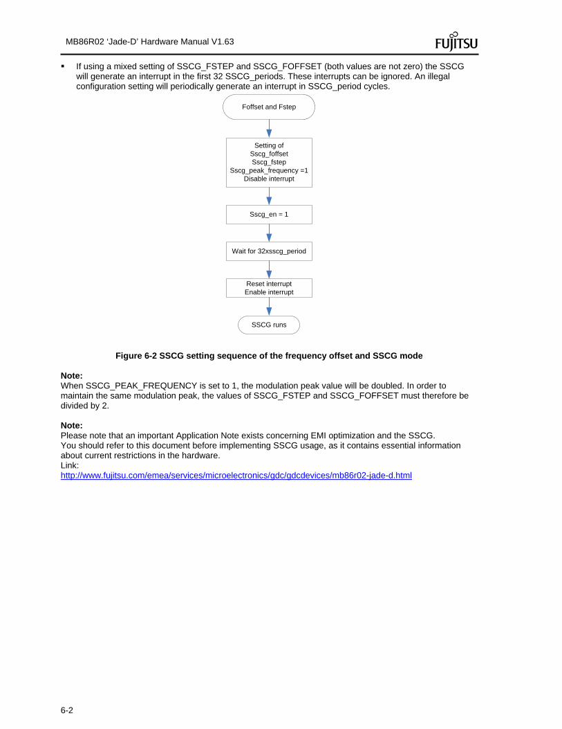
6-2
MB86R02 ‘Jade-D’ Hardware Manual V1.63
If using a mixed setting of SSCG_FSTEP and SSCG_FOFFSET (both values are not zero) the SSCG will generate an interrupt in the first 32 SSCG_periods. These interrupts can be ignored. An illegal configuration setting will periodically generate an interrupt in SSCG_period cycles.
Foffset and Fstep
Setting ofSscg_foffsetSscg_fstep
Sscg_peak_frequency =1Disable interrupt
Sscg_en = 1
Wait for 32xsscg_period
Reset interruptEnable interrupt
SSCG runs
Figure 6-2 SSCG setting sequence of the frequency offset and SSCG mode Note: When SSCG_PEAK_FREQUENCY is set to 1, the modulation peak value will be doubled. In order to maintain the same modulation peak, the values of SSCG_FSTEP and SSCG_FOFFSET must therefore be divided by 2. Note: Please note that an important Application Note exists concerning EMI optimization and the SSCG. You should refer to this document before implementing SSCG usage, as it contains essential information about current restrictions in the hardware. Link: http://www.fujitsu.com/emea/services/microelectronics/gdc/gdcdevices/mb86r02-jade-d.html
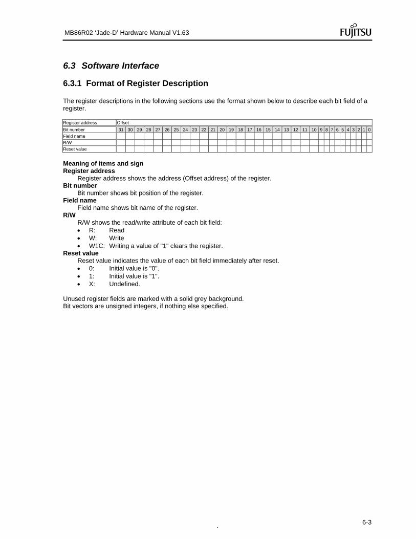
. 6-3
MB86R02 ‘Jade-D’ Hardware Manual V1.63
6.3 Software Interface
6.3.1 Format of Register Description The register descriptions in the following sections use the format shown below to describe each bit field of a register. Register address Offset
Bit number 31 30 29 28 27 26 25 24 23 22 21 20 19 18 17 16 15 14 13 12 11 10 9 8 7 6 5 4 3 2 1 0
Field name
R/W
Reset value
Meaning of items and sign Register address
Register address shows the address (Offset address) of the register. Bit number
Bit number shows bit position of the register. Field name
Field name shows bit name of the register. R/W
R/W shows the read/write attribute of each bit field: R: Read W: Write W1C: Writing a value of "1" clears the register.
Reset value Reset value indicates the value of each bit field immediately after reset. 0: Initial value is "0". 1: Initial value is "1". X: Undefined.
Unused register fields are marked with a solid grey background. Bit vectors are unsigned integers, if nothing else specified.
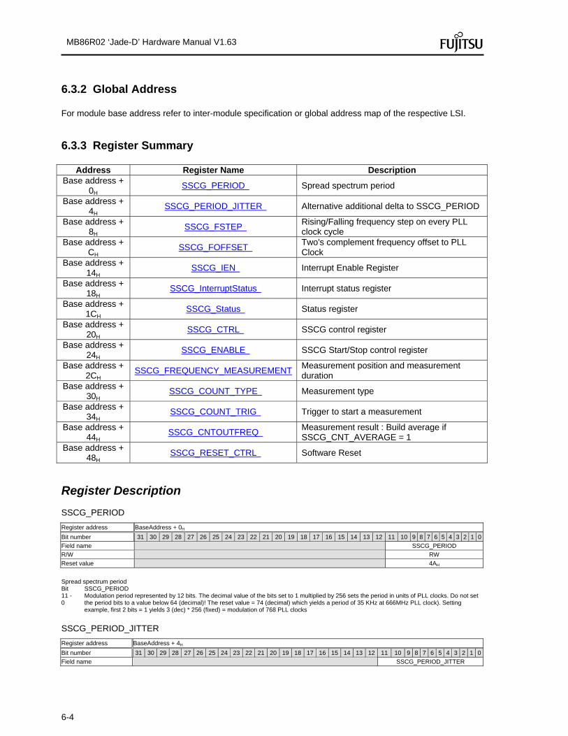
6-4
MB86R02 ‘Jade-D’ Hardware Manual V1.63
6.3.2 Global Address For module base address refer to inter-module specification or global address map of the respective LSI.
6.3.3 Register Summary
Address Register Name Description Base address +
0H SSCG_PERIOD Spread spectrum period
Base address + 4H
SSCG_PERIOD_JITTER Alternative additional delta to SSCG_PERIOD
Base address + 8H
SSCG_FSTEP Rising/Falling frequency step on every PLL clock cycle
Base address + CH
SSCG_FOFFSET Two's complement frequency offset to PLL Clock
Base address + 14H
SSCG_IEN Interrupt Enable Register
Base address + 18H
SSCG_InterruptStatus Interrupt status register
Base address + 1CH
SSCG_Status Status register
Base address + 20H
SSCG_CTRL SSCG control register
Base address + 24H
SSCG_ENABLE SSCG Start/Stop control register
Base address + 2CH
SSCG_FREQUENCY_MEASUREMENT Measurement position and measurement duration
Base address + 30H
SSCG_COUNT_TYPE Measurement type
Base address + 34H
SSCG_COUNT_TRIG Trigger to start a measurement
Base address + 44H
SSCG_CNTOUTFREQ Measurement result : Build average if SSCG_CNT_AVERAGE = 1
Base address + 48H
SSCG_RESET_CTRL Software Reset
Register Description SSCG_PERIOD
Register address BaseAddress + 0H
Bit number 31 30 29 28 27 26 25 24 23 22 21 20 19 18 17 16 15 14 13 12 11 10 9 8 7 6 5 4 3 2 1 0
Field name SSCG_PERIOD
R/W RW
Reset value 4AH
Spread spectrum period Bit 11 - 0
SSCG_PERIOD Modulation period represented by 12 bits. The decimal value of the bits set to 1 multiplied by 256 sets the period in units of PLL clocks. Do not set the period bits to a value below 64 (decimal)! The reset value = 74 (decimal) which yields a period of 35 KHz at 666MHz PLL clock). Setting example, first 2 bits = 1 yields 3 (dec) * 256 (fixed) = modulation of 768 PLL clocks
SSCG_PERIOD_JITTER
Register address BaseAddress + 4H
Bit number 31 30 29 28 27 26 25 24 23 22 21 20 19 18 17 16 15 14 13 12 11 10 9 8 7 6 5 4 3 2 1 0
Field name SSCG_PERIOD_JITTER

. 6-5
MB86R02 ‘Jade-D’ Hardware Manual V1.63
R/W RW
Reset value 3BH
Alternative additional delta to SSCG_PERIOD Bit 11 - 0
SSCG_PERIOD_JITTER 12 bits for modulation period jitter in PLL clock units, multiplied by a factor of 32. Example: decimal value of 3 means 3 PLL clocks jitter (*32) = 96 (Default value is 10% jitter to 35kHz default modulation period)
SSCG_FSTEP
Register address BaseAddress + 8H
Bit number 31 30 29 28 27 26 25 24 23 22 21 20 19 18 17 16 15 14 13 12 11 10 9 8 7 6 5 4 3 2 1 0
Field name SSCG_FSTEP
R/W RW
Reset value 209D6H
Rising/Falling frequency step on every PLL clock cycle Bit 31 - 0 SSCG_FSTEP
Frequency step per PLL clock. Default setting is +/-1.5% centre spread
SSCG_FOFFSET
Register address BaseAddress + CH
Bit number 31 30 29 28 27 26 25 24 23 22 21 20 19 18 17 16 15 14 13 12 11 10 9 8 7 6 5 4 3 2 1 0
Field name SSCG_FOFFSET
R/W RW
Reset value 0H
Two's complement frequency offset to PLL Clock Bit 31 - 0
SSCG_FOFFSET Two's complement offset of modulation frequency, 00000001: offset = 1, ffffffff offset = -1 0x147A E147 : +1% offset of modulated frequency 0x0A3D 70A3 : +0.5% offset of modulated frequency 0xF5C2 8F5D : -0.5% offset of modulated frequency 0xEB85 1EB9 : -1% offset of modulated frequency
SSCG_IEN
Register address BaseAddress + 14H
Bit number 31 30 29 28 27 26 25 24 23 22 21 20 19 18 17 16 15 14 13 12 11 10 9 8 7 6 5 4 3 2 1 0
Field name IEn_Frequency_Limit
R/W RW
Reset value 0H
Interrupt Enable Register Bit 0 IEn_Frequency_Limit
Interrupt enable (enables/disables interrupts using the respective field)
SSCG_InterruptStatus
Register address BaseAddress + 18H
Bit number 31 30 29 28 27 26 25 24 23 22 21 20 19 18 17 16 15 14 13 12 11 10 9 8 7 6 5 4 3 2 1 0
Field name ISts_Frequency_Limit
R/W RW
Reset value 0H
Interrupt status register Bit 0
ISts_Frequency_Limit Interrupt status flags, a '1' signifies that the corresponding interrupt condition occurred (even if the interrupt is disabled), writing a '1' clears the flag (a clear has a higher priority than setting)
SSCG_Status
Register address BaseAddress + 1CH
Bit number 31 30 29 28 27 26 25 24 23 22 21 20 19 18 17 16 15 14 13 12 11 10 9 8 7 6 5 4 3 2 1 0
Field name Sts_Frequency_Limit
R/W R
Reset value 0H
Status register Bit 0 Sts_Frequency_Limit
0: normal operational frequency, 1: maximum frequency exceeded
SSCG_CTRL
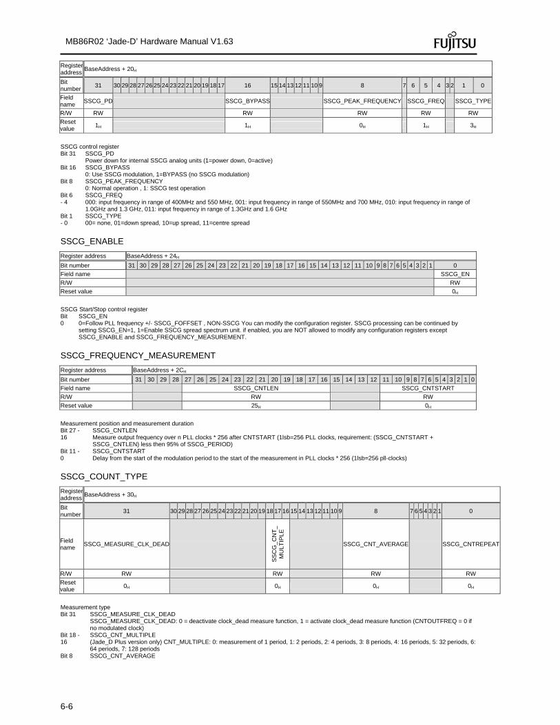
6-6
MB86R02 ‘Jade-D’ Hardware Manual V1.63
Register address
BaseAddress + 20H
Bit number
31 30 29 28 27 26 25 24 23 22 21 20 19 18 17 16 15 14 13 12 11 10 9 8 7 6 5 4 3 2 1 0
Field name
SSCG_PD SSCG_BYPASS SSCG_PEAK_FREQUENCY SSCG_FREQ SSCG_TYPE
R/W RW RW RW RW RW
Reset value
1H 1H 0H 1H 3H
SSCG control register Bit 31 SSCG_PD
Power down for internal SSCG analog units (1=power down, 0=active) Bit 16 SSCG_BYPASS
0: Use SSCG modulation, 1=BYPASS (no SSCG modulation) Bit 8 SSCG_PEAK_FREQUENCY
0: Normal operation , 1: SSCG test operation Bit 6 - 4
SSCG_FREQ 000: input frequency in range of 400MHz and 550 MHz, 001: input frequency in range of 550MHz and 700 MHz, 010: input frequency in range of 1.0GHz and 1.3 GHz, 011: input frequency in range of 1.3GHz and 1.6 GHz
Bit 1 - 0
SSCG_TYPE 00= none, 01=down spread, 10=up spread, 11=centre spread
SSCG_ENABLE
Register address BaseAddress + 24H
Bit number 31 30 29 28 27 26 25 24 23 22 21 20 19 18 17 16 15 14 13 12 11 10 9 8 7 6 5 4 3 2 1 0
Field name SSCG_EN
R/W RW
Reset value 0H
SSCG Start/Stop control register Bit 0
SSCG_EN 0=Follow PLL frequency +/- SSCG_FOFFSET , NON-SSCG You can modify the configuration register. SSCG processing can be continued by setting SSCG_EN=1, 1=Enable SSCG spread spectrum unit. if enabled, you are NOT allowed to modify any configuration registers except SSCG_ENABLE and SSCG_FREQUENCY_MEASUREMENT.
SSCG_FREQUENCY_MEASUREMENT
Register address BaseAddress + 2CH
Bit number 31 30 29 28 27 26 25 24 23 22 21 20 19 18 17 16 15 14 13 12 11 10 9 8 7 6 5 4 3 2 1 0
Field name SSCG_CNTLEN SSCG_CNTSTART
R/W RW RW
Reset value 25H 0H
Measurement position and measurement duration Bit 27 - 16
SSCG_CNTLEN Measure output frequency over n PLL clocks * 256 after CNTSTART (1lsb=256 PLL clocks, requirement: (SSCG_CNTSTART + SSCG_CNTLEN) less then 95% of SSCG_PERIOD)
Bit 11 - 0
SSCG_CNTSTART Delay from the start of the modulation period to the start of the measurement in PLL clocks * 256 (1lsb=256 pll-clocks)
SSCG_COUNT_TYPE
Register address
BaseAddress + 30H
Bit number
31 30 29 28 27 26 25 24 23 22 21 20 19 18 17 16 15 14 13 12 11 10 9 8 7 6 5 4 3 2 1 0
Field name
SSCG_MEASURE_CLK_DEAD
SS
CG
_CN
T_
MU
LTIP
LE
SSCG_CNT_AVERAGE SSCG_CNTREPEAT
R/W RW RW RW RW
Reset value
0H 0H 0H 0H
Measurement type Bit 31 SSCG_MEASURE_CLK_DEAD
SSCG_MEASURE_CLK_DEAD: 0 = deactivate clock_dead measure function, 1 = activate clock_dead measure function (CNTOUTFREQ = 0 if no modulated clock)
Bit 18 - 16
SSCG_CNT_MULTIPLE (Jade_D Plus version only) CNT_MULTIPLE: 0: measurement of 1 period, 1: 2 periods, 2: 4 periods, 3: 8 periods, 4: 16 periods, 5: 32 periods, 6: 64 periods, 7: 128 periods
Bit 8 SSCG_CNT_AVERAGE

. 6-7
MB86R02 ‘Jade-D’ Hardware Manual V1.63
(Jade_D Plus version only) CNT_AVERAGE: 0 = non calculate average, 1 = calculate average e.g. for MULTIPLE = 2 (AVERAGE = 0 SSCG_OUTFREQ = h8023, AVERAGE = 1 SSCG_OUTFREQ = h2008)
Bit 0 SSCG_CNTREPEAT CNTREPEAT: 0 = one measurement, 1 = continuous measurement
SSCG_COUNT_TRIG
Register address BaseAddress + 34H
Bit number 31 30 29 28 27 26 25 24 23 22 21 20 19 18 17 16 15 14 13 12 11 10 9 8 7 6 5 4 3 2 1 0
Field name SSCG_CNTTRIG
R/W W
Reset value 0H
Trigger to start a measurement Bit 0 SSCG_CNTTRIG
Used for debugging: write 1 to trigger a measurement (if sscg_cntrepeat=0)
SSCG_CNTOUTFREQ
Register address BaseAddress + 44H
Bit number 31 30 29 28 27 26 25 24 23 22 21 20 19 18 17 16 15 14 13 12 11 10 9 8 7 6 5 4 3 2 1 0
Field name SSCG_OUTFREQ
R/W R
Reset value 0H
Measurement result : Build average if SSCG_CNT_AVERAGE = 1 Bit 24 - 0 SSCG_OUTFREQ
Used for debugging: Measured output clock count
SSCG_RESET_CTRL
Register address BaseAddress + 48H
Bit number 31 30 29 28 27 26 25 24 23 22 21 20 19 18 17 16 15 14 13 12 11 10 9 8 7 6 5 4 3 2 1 0
Field name SWreset_delay SSCG_SWreset
R/W RW RW
Reset value 80H 0H
Software Reset Bit 15 - 8
SWreset_delay 0= normal operation, 1=Software reset. SSCG is reset during SSCG_SWreset=1 plus SWreset_delay * 8 of PLL clock (by default: SSCG_SWreset=1 + 8*128 PLL clock)
Bit 0 SSCG_SWreset 0= normal operation, 1=Software reset. SSCG is reset during SSCG_SWreset=1 plus SWreset_delay * 8 of PLL clock

6-8
MB86R02 ‘Jade-D’ Hardware Manual V1.63
6.4 Processing Mode
6.4.1 Parameter setting for 666MHz PLL clock • All register values in the following tables are valid for PLL clock = 666MHz
6.4.1.1 Parameter setting for SSCG-speed of 15KHz Given: SSCG_ FREQUENCY_OFFSET = 0 (default), SSCG_PEAK_FREQUENCY = 0 (default) SSCG_PERIOD_JITTER = 10 % (default)
SSCG_TYPE SSCG_PERIOD PERIOD_DELTA Modulation Peak % SSCG_STEP
3 Center Spread
0xAC 0x8A
0.5 0x6ED0 1.0 0xDDA0 1.5 0x1 4C70 2.0 0x1 BB40 2.5 0x2 2A10 3.0 0x2 9820
2 Upspread
0xAC 0x8A
0.5 0x3768 1.0 0x6ED0 1.5 0xA638 2.0 0xDDA0 2.5 0x1 1508 3.0 0x1 4C70
1 Downspread
0xAC 0x8A
0.5 0x3768 1.0 0x6ED0 1.5 0xA638 2.0 0xDDA0 2.5 0x1 1508 3.0 0x1 4C70
Table 6-3 SSCG speed of 15KHz (refer to 666MHz PLL clock)

. 6-9
MB86R02 ‘Jade-D’ Hardware Manual V1.63
6.4.1.2 Parameter setting for SSCG-speed of 20KHz Given: SSCG_ FREQUENCY_OFFSET = 0 (default), PERIOD_DELTA = 10 % SSCG_PEAK_FREQUENCY = 0 SSCG_TYPE SSCG_PERIOD PERIOD_DELTA Modulation Peak % SSCG_STEP
3 Centre Spread
0x7B 0x70 0.5 0x9913 1.0 0x1 3226 1.5 0x1 CB39
2 Upspread
0x7B 0x70 0.5 0x4C89 1.0 0x9913 1.5 0xE59B
1 Downspread
0x7B 0x70 0.5 0x4C89 1.0 0x9913 1.5 0xE59B
Table 6-4 SSCG speed of 20KHz (refer to 666MHz PLL clock)

6-10
MB86R02 ‘Jade-D’ Hardware Manual V1.63
6.4.1.3 Parameter setting for SSCG-speed of 35KHz Given: SSCG_ FREQUENCY_OFFSET = 0(default), SSCG_PEAK = 0(default) SSCG_PERIOD_JITTER = 10 %(default)
SSCG_TYPE SSCG_PERIOD SSCG_PERIOD_JITTER Modulation Peak % SSCG_STEP
3 Center spread
0x49 0x3B
0.5 0x1 04EB 1.0 0x209D6 1.5 0x3 0EC1 2.0 0x4 13AC 2.5 0x5 1897 3.0 0x6 1D82
2 Upspread
0x49 0x3B
0.5 0x8275 1.0 0x1 04EB 1.5 0x1 875F 2.0 0x209D6 2.5 0x2 8C49 3.0 0x3 0EC1
1 Downspread
0x49 0x3B
0.5 0x8275 1.0 0x1 04EB 1.5 0x1 875F 2.0 0x209D6 2.5 0x2 8C49 3.0 0x3 0EC1
Table 6-5 SSCG speed of 35KHz (refer to 666MHz PLL clock)
6.4.1.4 Parameter setting for SSCG-speed of 50KHz Given: SSCG_ FREQUENCY_OFFSET = 0(default) SSCG_PEAK = 0(default) SSCG_PERIOD_JITTER = 10 %(default)
SSCG_TYPE SSCG_PERIOD SSCG_PERIOD_JITTER Modulation Peak % SSCG_STEP
3 Center spread
0x33 0x29
0.5 0x1 75A8 1.0 0x2 EB50 1.5 0x460F8 2.0 0x5D6A1 2.5 0x74C49 3.0 0x8C1F1
2 Upspread
0x33 0x29
0.5 0xBAD4 1.0 0x1 75A8 1.5 0x2 307C 2.0 0x2 EB50 2.5 0x3 A624 3.0 0x460F8
1 Downspread
0x33 0x29
0.5 0xBAD4 1.0 0x1 75A8 1.5 0x2 307C 2.0 0x2 EB50 2.5 0x3 A624 3.0 0x460F8
Table 6-6 SSCG speed of 50KHz (refer to 666MHz PLL clock)

. 6-11
MB86R02 ‘Jade-D’ Hardware Manual V1.63
6.5 Control Flow
6.5.1 Operation The configuration parameters of the SSCG unit can be programmed as shown below:
Sscg_period = 35KHzSscg_period_period= 10%
Centre spreadSscg degree = +/-1.5%
No frequency offsetdisable interrupt
Default setting
Desired Indiviual setting?
Start SSCG by setting SSCG_ENABLE =1
ChangeConfiguration?
SSCG_ENABLE = 0
reset
SSCG runs
NO
YES
NO
YES
Refer to Table 1,Table5, Table6, Table7
666MHz PLL clock
Figure 6-7 SSCG programming flow

7-1
MB86R02 ‘Jade-D’ Hardware Manual V1.63
7 CCNT (Chip Control) This chapter describes the functionality and operation of the Chip Control Module (CCNT).
7.1 Overview
The Chip Control Module (referred to from here on as CCNT) is an INT signal (interrupt) conversion process (pulse → level) from each module and it controls soft resets, the AXI priority level and AXI BUS Waits (MBUS2AXI Bridge exclusive use).

7-2
MB86R02 ‘Jade-D’ Hardware Manual V1.63
7.2 Features
The pin multiplex interface o Selects the multiplex mode for various pins (see also chapter 1)
The external pin interface o Displays the signal level of the external pin in status.
The MediaLB interface Switches the method of MediaLB of the AHB read data output.
7.3 Supply clock
The APB clock signal is supplied to the CCNT module. Please refer to chpater 5 'Clock Reset Generator' for information about setting the frequency and the control specifications of the APB clock.
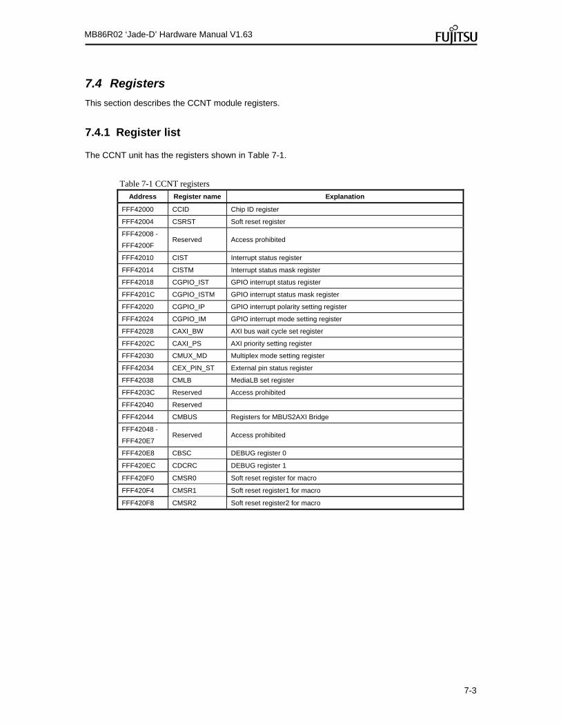
7-3
MB86R02 ‘Jade-D’ Hardware Manual V1.63
7.4 Registers
This section describes the CCNT module registers.
7.4.1 Register list
The CCNT unit has the registers shown in Table 7-1.
Table 7-1 CCNT registers
Address Register name Explanation
FFF42000 CCID Chip ID register
FFF42004 CSRST Soft reset register
FFF42008 -
FFF4200F Reserved Access prohibited
FFF42010 CIST Interrupt status register
FFF42014 CISTM Interrupt status mask register
FFF42018 CGPIO_IST GPIO interrupt status register
FFF4201C CGPIO_ISTM GPIO interrupt status mask register
FFF42020 CGPIO_IP GPIO interrupt polarity setting register
FFF42024 CGPIO_IM GPIO interrupt mode setting register
FFF42028 CAXI_BW AXI bus wait cycle set register
FFF4202C CAXI_PS AXI priority setting register
FFF42030 CMUX_MD Multiplex mode setting register
FFF42034 CEX_PIN_ST External pin status register
FFF42038 CMLB MediaLB set register
FFF4203C Reserved Access prohibited
FFF42040 Reserved
FFF42044 CMBUS Registers for MBUS2AXI Bridge
FFF42048 -
FFF420E7 Reserved Access prohibited
FFF420E8 CBSC DEBUG register 0
FFF420EC CDCRC DEBUG register 1
FFF420F0 CMSR0 Soft reset register for macro
FFF420F4 CMSR1 Soft reset register1 for macro
FFF420F8 CMSR2 Soft reset register2 for macro

7-4
MB86R02 ‘Jade-D’ Hardware Manual V1.63
Format of Register Descriptions The register descriptions in the following sections use the format shown below to describe each bit field of a register.
Address Base address + Offset
Bit 31 30 29 28 27 26 25 24 23 22 21 20 19 18 17 16
Name
R/W
Initial value
Bit 15 14 13 12 11 10 9 8 7 6 5 4 3 2 1 0
Name
R/W
Initial value
Meaning of items and sign Address
Address shows the address (Base address + Offset address) of the register. Bit
Bit shows bit number of the register. Name
Name shows bit field name of the register. R/W
R/W shows the read/write attribute of each bit field: R0: The read value is always "0". R1: The read value is always "1". W0: The write value is always "0". If "1" is written, it is ignored. W1: The write value is always "1". If "0" is written, it is ignored. R: Read W: Write
Initial value Initial value indicates the value of each bit field immediately after reset. 0: Initial value is "0". 1: Initial value is "1". X: Undefined.
7-5
MB86R02 ‘Jade-D’ Hardware Manual V1.63
7.4.2 CHIP ID register (CCID)
Address FFF4_2000 + 00h
Bit 31 30 29 28 27 26 25 24 23 22 21 20 19 18 17 16
Name YEAR[15:0]
R/W R R R R R R R R R R R R R R R R
Initial value 0 0 1 0 0 0 0 0 0 0 0 0 1 0 0 0
Bit 15 14 13 12 11 10 9 8 7 6 5 4 3 2 1 0
Name CHIPNAME[7:0] VERSION[7:0]
R/W R R R R R R R R R R R R R R R R
Initial value 0 0 0 1 0 0 0 1 0 0 0 0 0 0 0 0
Bit field Function
Number Name
31-16 YEAR[15:0] Development year of the GDC as four digits.
For this GDC it reads 2010(h).
15-8 CHIPNAME[7:0] LSI identification name is shown by the identification number. For this GDC it reads 11(h).
7-0 VERSION[7:0]
The version of the GDC is shown. The GDC reports the following values:
ES1 version: 00(h)
ES2 version: 01(h)
MCS version: 02(h)
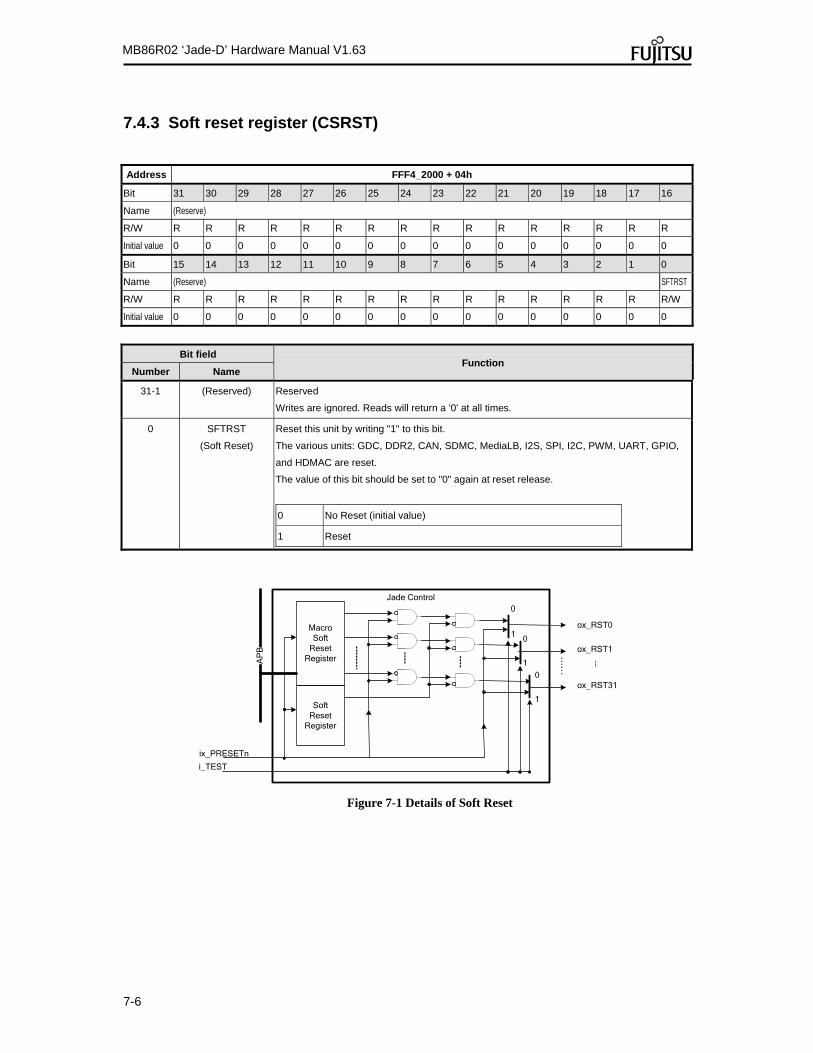
7-6
MB86R02 ‘Jade-D’ Hardware Manual V1.63
7.4.3 Soft reset register (CSRST)
Address FFF4_2000 + 04h
Bit 31 30 29 28 27 26 25 24 23 22 21 20 19 18 17 16
Name (Reserve)
R/W R R R R R R R R R R R R R R R R
Initial value 0 0 0 0 0 0 0 0 0 0 0 0 0 0 0 0
Bit 15 14 13 12 11 10 9 8 7 6 5 4 3 2 1 0
Name (Reserve) SFTRST
R/W R R R R R R R R R R R R R R R R/W
Initial value 0 0 0 0 0 0 0 0 0 0 0 0 0 0 0 0
Bit field Function
Number Name
31-1 (Reserved) Reserved
Writes are ignored. Reads will return a '0' at all times.
0 SFTRST
(Soft Reset)
Reset this unit by writing "1" to this bit.
The various units: GDC, DDR2, CAN, SDMC, MediaLB, I2S, SPI, I2C, PWM, UART, GPIO,
and HDMAC are reset.
The value of this bit should be set to "0" again at reset release.
0 No Reset (initial value)
1 Reset
Jade Control
MacroSoft
ResetRegisterA
PB
SoftReset
Register
ix_PRESETn
ox_RST0
ox_RST1
ox_RST31
i_TEST
0
1 0
0
1
1
Figure 7-1 Details of Soft Reset

7-7
MB86R02 ‘Jade-D’ Hardware Manual V1.63
7.4.4 Interrupt status register (CIST)
Address FFF4_2000 + 10h
Bit 31 30 29 28 27 26 25 24 23 22 21 20 19 18 17 16
Name INT31 (Reserved) INT28 INT27 INT26 INT25 INT24 (Reserved)
R/W R/W R/W R/W R/W R/W R/W R/W R/W R/W R/W R/W R/W R/W R/W R/W R/W
Initial value 0 0 0 0 0 0 0 0 0 0 0 0 0 0 0 0
Bit 15 14 13 12 11 10 9 8 7 6 5 4 3 2 1 0
Name (Reserved) INT5 (Reserved)
R/W R/W R/W R/W R/W R/W R/W R/W R/W R/W R/W R/W R/W R/W R/W R/W R/W
Initial value 0 0 0 0 0 0 0 0 0 0 0 0 0 0 0 0
Bit field Function
Number Name
31 INT31
(MediaLB DINT)
This bit is set to '1' if i_int31 becomes '1'.
Clearing is done by writing a '0' to this bit.
If Bit31 of the INT Mask register is set to mask "0", this bit is fixed at "0".
0 There is no interrupt. (initial value)
1 There is an interruption.
30-29 (Reserved) Reserved
Writes are ignored. Reads will return a '0' at all times.
28 INT28
(HBUS2AXI)
This bit is set to '1' if i_int28 becomes '1'.
Clearing is done by writing a '0' to this bit.
If Bit28 of the INT Mask register is set to mask "0", this bit is fixed at "0".
0 There is no interrupt. (initial value)
1 There is an interruption.
27 INT27 (MBUS2AXI
(Draw))
This bit is set to '1' if i_int27 becomes '1'.
Clearing is done by writing a '0' to this bit.
If Bit28 of the INT Mask register is set to mask "0", this bit is fixed at "0".
0 There is no interrupt. (initial value)
1 There is an interruption.
26 INT26 (MBUS2AXI
(DispCap))
This bit is set to '1' if i_int26 becomes '1'.
Clearing is done by writing a '0' to this bit.
If Bit26 of the INT Mask register is set to mask "0", this bit is fixed at "0".
0 There is no interrupt. (initial value)
1 There is an interruption.
25 INT25
(AHB2AXI
(CPUroot))
This bit is set to '1' if i_int25 becomes '1'.
Clearing is done by writing a '0' to this bit.
If Bit25 of the INT Mask register is set to mask "0", this bit is fixed at "0".

7-8
MB86R02 ‘Jade-D’ Hardware Manual V1.63
Bit field Function
Number Name
0 There is no interrupt. (initial value)
1 There is an interruption.
24 INT24
(AHB2AXI
(AHBBus))
This bit is set to '1' if i_int24 becomes '1'.
Clearing is done by writing a '0' to this bit.
If Bit24 of the INT Mask register is set to mask "0", this bit is fixed at "0".
0 There is no interrupt. (initial value)
1 There is an interruption.
23-6 (Reserved) Reserved
Writes are ignored. Reads will return a '0' at all times.
5 INT5 (MBUS2AXI
(Cap) )
This bit is set to '1' if i_int5 becomes '1'.
Clearing is done by writing a '0' to this bit.
If Bit5 of the INT Mask register is set to mask "0", this bit is fixed at "0".
0 There is no interrupt. (initial value)
1 There is an interruption.
4 -1 (Reserved)
0 (Reserved) Reserved
Writes are ignored. Reads will return a '0' at all times.

7-9
MB86R02 ‘Jade-D’ Hardware Manual V1.63
7.4.5 Interrupt status mask register (CISTM)
Address FFF4_2000 + 14h
Bit 31 30 29 28 27 26 25 24 23 22 21 20 19 18 17 16
Name INT31M
ASK (Reserved)
INT28M
ASK
INT27M
ASK
INT26M
ASK
INT25M
ASK
INT24M
ASK (Reserved)
R/W R/W R/W R/W R/W R/W R/W R/W R/W R/W R/W R/W R/W R/W R/W R/W R/W
Initial value 0 0 0 0 0 0 0 0 0 0 0 0 0 0 0 0
Bit 15 14 13 12 11 10 9 8 7 6 5 4 3 2 1 0
Name (Reserved) INT5
MASK (Res)
INT3
MASK
INT2
MASK
INT1
MASK
INT0
MASK
R/W R/W R/W R/W R/W R/W R/W R/W R/W R/W R/W R/W R/W R/W R/W R/W R/W
Initial value 0 0 0 0 0 0 0 0 0 0 0 0 0 0 0 0
Bit field Function
Number Name
31 INT31 Mask Interrupt for MediaLB. INT information becomes valid by writing "1" to this bit.
0 Mask (initial value)
1 INT31 valid
30-29 (Reserved) Reserved
Writes are ignored. Reads will return a '0' at all times.
28 INT28 Mask Interrupt for HBUS2AXI. INT information becomes valid by writing "1" to this bit.
0 Mask (initial value)
1 INT28 valid
27 INT27 Mask Interrupt for MBUS2AXI Draw. INT information becomes valid by writing "1" to this bit.
0 Mask (initial value)
1 INT27 valid
26 INT26 Mask Interrupt for MBUS2AXI Display Capture. INT information becomes valid by writing "1" to this
bit.
0 Mask (initial value)
1 INT26 valid
25 INT25 Mask Interrupt for AHB2AXI. INT information becomes valid by writing "1" to this bit.
0 Mask (initial value)
1 INT25 valid
24 INT24 Mask Interrupt for AHB2AXI (AHB Bus). INT information becomes valid by writing "1" to this bit.
0 Mask (initial value)

7-10
MB86R02 ‘Jade-D’ Hardware Manual V1.63
Bit field Function
Number Name
1 INT24 valid
23-6 (Reserved) Reserved
Writes are ignored. Reads will return a '0' at all times.
5 INT5 Mask Interrupt for MBUS2AXI Capture. INT information becomes valid by writing "1" to this bit.
0 Mask (initial value)
1 INT5 valid
4 (Reserved) Reserved
Writes are ignored. Reads will return a '0' at all times.
3 INT3 Mask ADC3 interrupt mask. INT information becomes valid by writing "1" to this bit.
0 Mask (initial value)
1 INT3 valid
2 INT2 Mask ADC2 interrupt mask. INT information becomes valid by writing "1" to this bit.
0 Mask (initial value)
1 INT2 valid
1 INT1 Mask ADC1 interrupt mask. INT information becomes valid by writing "1" to this bit.
0 Mask (initial value)
1 INT1 valid
0 INT0 Mask ADC0 interrupt mask. INT information becomes valid by writing "1" to this bit.
0 Mask (initial value)
1 INT0 valid
7-11
MB86R02 ‘Jade-D’ Hardware Manual V1.63
7.4.6 GPIO interrupt status register (CGPIO_IST)
This register shows the status of the interrupt that relates to GPIO.
Address FFF4_2000 + 18h
Bit 31 30 29 28 27 26 25 24 23 22 21 20 19 18 17 16
Name (Reserved) GPIO_INT_status[23:16]
R/W R0/W
0
R0/W
0
R0/W
0
R0/W
0
R0/W
0
R0/W
0
R0/W
0
R0/W
0 R/W0 R/W0 R/W0 R/W0 R/W0 R/W0 R/W0 R/W0
Initial value 0 0 0 0 0 0 0 0 0 0 0 0 0 0 0 0
Bit 15 14 13 12 11 10 9 8 7 6 5 4 3 2 1 0
Name GPIO_INT_status[15:0]
R/W R/W0 R/W0 R/W0 R/W0 R/W0 R/W0 R/W0 R/W0 R/W0 R/W0 R/W0 R/W0 R/W0 R/W0 R/W0 R/W0
Initial value 0 0 0 0 0 0 0 0 0 0 0 0 0 0 0 0
Bit field Function
Number Name
31-24 (Reserved) Reserved
Writes are ignored. Reads will return a '0' at all times.
23-0 GPIO_INT_status
(GPIO interrupt
status)
Clear by writing '0'.
Indicates a GPIO interrupt.
0 No interrupt occurred.
1 Interrupt occurred.
7.4.7 GPIO interrupt status mask register (CGPIO_ISTM)
This register controls GPIO related interrupts. It is used to mask the interrupt status of each GPIO interrupt. The register takes effect regardless of the input/output situation at the time it is set. Each bit that can be set corresponds to an interrupt that can be masked.
Address FFF4_2000 + 1Ch
Bit 31 30 29 28 27 26 25 24 23 22 21 20 19 18 17 16
Name (Reserved) GPIO_INT_enable[23:16]
R/W R0/W
0
R0/W
0
R0/W
0
R0/W
0
R0/W
0
R0/W
0
R0/W
0
R0/W
0 R/W R/W R/W R/W R/W R/W R/W R/W
Initial value 0 0 0 0 0 0 0 0 0 0 0 0 0 0 0 0
Bit 15 14 13 12 11 10 9 8 7 6 5 4 3 2 1 0
Name GPIO_INT_enable[15:0]
R/W R/W R/W R/W R/W R/W R/W R/W R/W R/W R/W R/W R/W R/W R/W R/W R/W
Initial value 0 0 0 0 0 0 0 0 0 0 0 0 0 0 0 0
Bit field Function
Number Name

7-12
MB86R02 ‘Jade-D’ Hardware Manual V1.63
31-24 (Reserved) Reserved
Writes are ignored. Reads will return a '0' at all times.
23-0 GPIO_INT_enable
(GPIO interrupt
enable)
Set whether the interrupt of each bit occurs according to the value which the external pins
GPIO23-0 sample with the internal clock.
0 Interrupt doesn't occur.
1 Occur interrupt based on the following register setting.

7-13
MB86R02 ‘Jade-D’ Hardware Manual V1.63
7.4.8 GPIO interrupt polarity setting register (CGPIO_IP)
This register controls the polarity detection type for GPIO interrupts. The register takes effect regardless of the input/output situation at the time it is set. Each bit that can be set corresponds to an interrupt that can be configured.
Address FFF4_2000 + 20h
Bit 31 30 29 28 27 26 25 24 23 22 21 20 19 18 17 16
Name (Reserved) GPIO_INT_polarity[23:16]
R/W R0/W
0
R0/W
0
R0/W
0
R0/W
0
R0/W
0
R0/W
0
R0/W
0
R0/W
0 R/W R/W R/W R/W R/W R/W R/W R/W
Initial value 0 0 0 0 0 0 0 0 0 0 0 0 0 0 0 0
Bit 15 14 13 12 11 10 9 8 7 6 5 4 3 2 1 0
Name GPIO_INT_polarity[15:0]
R/W R/W R/W R/W R/W R/W R/W R/W R/W R/W R/W R/W R/W R/W R/W R/W R/W
Initial value 0 0 0 0 0 0 0 0 0 0 0 0 0 0 0 0
Bit field Function
Number Name
31-24 (Reserved) Reserved
Writes are ignored. Reads will return a '0' at all times.
23-0 GPIO_INT_polarity
(GPIO interrupt
polarity)
An interrupt occurs according to the following values.
0 Detect on level "0" or negative edge (depends on GPIO_INT_mode)
1 Detect on level "1" or positive edge (depends on GPIO_INT_mode)
7.4.9 GPIO interrupt mode setting register (CGPIO_IM)
This register controls the level/edge mode detection type for GPIO interrupts. The register takes effect regardless of the input/output situation at the time it is set. Each bit that can be set corresponds to an interrupt that can be configured.
Address FFF4_2000 + 24h
Bit 31 30 29 28 27 26 25 24 23 22 21 20 19 18 17 16
Name (Reserved) GPIO_INT_mode[23:16]
R/W R0/W
0
R0/W
0
R0/W
0
R0/W
0
R0/W
0
R0/W
0
R0/W
0
R0/W
0 R/W R/W R/W R/W R/W R/W R/W R/W
Initial value 0 0 0 0 0 0 0 0 0 0 0 0 0 0 0 0
Bit 15 14 13 12 11 10 9 8 7 6 5 4 3 2 1 0
Name GPIO_INT_mode[15:0]
R/W R/W R/W R/W R/W R/W R/W R/W R/W R/W R/W R/W R/W R/W R/W R/W R/W
Initial value 0 0 0 0 0 0 0 0 0 0 0 0 0 0 0 0
Bit field Function
Number Name
31-16 (Reserved) Reserved

7-14
MB86R02 ‘Jade-D’ Hardware Manual V1.63
Writes are ignored. Reads will return a '0' at all times.
23-0 GPIO_INT_mode GPIO_INT_mode (GPIO interrupt mode)
0 Level sensitive ('0' or '1' depends on GPIO_INT_polarity)
1 Edging sensitive ('Pos' or ‘neg' is shown in GPIO_INT_polarity)

7-15
MB86R02 ‘Jade-D’ Hardware Manual V1.63
7.4.10 AXI bus wait cycle set register (CAXI_BW)
Address FFF4_2000 + 28h
Bit 31 30 29 28 27 26 25 24 23 22 21 20 19 18 17 16
Name Disp_RWait[3:0] Disp_WWait[3:0] Draw_RWait[3:0] Draw_WWait[3:0]
R/W R/W R/W R/W R/W R/W R/W R/W R/W R/W R/W R/W R/W R/W R/W R/W R/W
Initial value 0 0 0 0 0 0 0 0 0 0 0 0 0 0 0 0
Bit 15 14 13 12 11 10 9 8 7 6 5 4 3 2 1 0
Name CPU_RWait[3:0] CPU_WWait[3:0] PrimaryAHB_RWait[3:0] PrimaryAHB_WWait[3:0]
R/W R/W R/W R/W R/W R/W R/W R/W R/W R/W R/W R/W R/W R/W R/W R/W R/W
Initial value 0 0 0 0 0 0 0 0 0 0 0 0 0 0 0 0
Bit field Function
Number Name
31-28 Disp_RWait
(Read Wait)
The Wait time of AXI Write BUS of MBUS2AXI Bridge (between the transactions) can be set by
this bit.
This setting can set even 0H(No Wait) - FH(15Cycle Wait).
The initial value is 0H(No Wait).
Note: 1Cycle is AXI 1Clock.
27-24 Disp_WWAIT
(Write Wait)
The Wait time of AXI Read BUS of MBUS2AXI Bridge (between the transactions) can be set by
this bit.
This setting can set even 0H(No Wait) - FH(15Cycle Wait).
The initial value is 0H(No Wait).
Note: 1Cycle is AXI 1Clock.
23-20 Draw_RWAIT
(Read Wait)
The Wait time of AXI Write BUS of MBUS2AXI Bridge (between the transactions) can be set by
this bit.
This setting can set even 0H(No Wait) - FH(15Cycle Wait).
The initial value is 0H(No Wait).
Note: 1Cycle is AXI 1Clock.
19-16 Draw_WWAIT
(Write Wait)
The Wait time of AXI Read BUS of MBUS2AXI Bridge (between the transactions) can be set by
this bit.
This setting can set even 0H(No Wait) - FH(15Cycle Wait).
The initial value is 0H(No Wait).
Note: 1Cycle is AXI 1Clock.
15-12 CPU_RWAIT
(Read Wait)
The Wait time of AXI Write BUS of AHB2AXI Bridge (between the transactions) can be set by this
bit.
This setting can set even 0H(No Wait) - FH(15Cycle Wait).
The initial value is 0H(No Wait).
Note: 1Cycle is AXI 1Clock.
11-8 CPU_WWait
(Write Wait)
The Wait time of AXI Read BUS of AHB2AXI Bridge (between the transactions) can be set by this
bit.
This setting can set even 0H(No Wait) - FH(15Cycle Wait).
The initial value is 0H(No Wait).

7-16
MB86R02 ‘Jade-D’ Hardware Manual V1.63
Bit field Function
Number Name
Note: 1Cycle is AXI 1Clock.
7-4 PrimaryAHB_RWAI
T (Write Wait)
The Wait time of AXI Write BUS of AHB2AXI Bridge (between the transactions) can be set by this
bit.
This setting can set even 0H(No Wait) - FH(15Cycle Wait).
The initial value is 0H(No Wait).
Note: 1Cycle is AXI 1Clock.
3-0 PrimaryAHB_WWAI
T (Read Wait)
The Wait time of AXI Read BUS of AHB2AXI Bridge (between the transactions) can be set by this
bit.
This setting can set even 0H(No Wait) - FH(15Cycle Wait).
The initial value is 0H(No Wait).
Note: 1Cycle is AXI 1Clock.

7-17
MB86R02 ‘Jade-D’ Hardware Manual V1.63
7.4.11 AXI priority setting register (CAXI_PS)
Sets the priority level of the AXI interconnect bus. Use the bitfield to set a priority level in the range of 0 ... 4. Do not set a value of 5 or more. If you do so, the write will be ignored and the previous value maintained.
Address FFF4_2000 + 2Ch
Bit 31 30 29 28 27 26 25 24 23 22 21 20 19 18 17 16
Name (Reserved) P_SEL4
R/W R R R R R R R R R R R R R R/W R/W R/W
Initial value 0 0 0 0 0 0 0 0 0 0 0 0 0 1 0 0
Bit 15 14 13 12 11 10 9 8 7 6 5 4 3 2 1 0
Name (Reserved) P_SEL3 (Reserved) P_SEL2 (Reserved) P_SEL1 (Reserved) P_SEL0
R/W R R/W R/W R/W R R/W R/W R/W R R/W R/W R/W R R/W R/W R/W
Initial value 0 1 0 0 0 0 1 0 0 0 0 1 0 0 0 0
Bit field Function
Number Name
31-19 (Reserved) Reserved
Writes are ignored. Reads will return a '0' at all times.
18-16 P_SEL4
(Priority Select4)
The priority level of AXI interconnect bus can be set by this bitfield.
000 0
001 1
010 2
011 3
100 4 (initial value)
15 (Reserved) Reserved
Writes are ignored. Reads will return a '0' at all times.
14-12 P_SEL3
(Priority Select3)
The priority level of AXI interconnect bus can be set by this bit.
000 DispCap
001 AHB
010 CPU
011 HBUS(initial value)
100 DRAW
11 (Reserved) Reserved
Writes are ignored. Reads will return a '0' at all times.
10-8 P_SEL2
(Priority Select2)
The priority level of AXI interconnect bus can be set by this bit.
000 DispCap
001 AHB
010 CPU(initial value)
011 HBUS
7-18
MB86R02 ‘Jade-D’ Hardware Manual V1.63
Bit field Function
Number Name
100 DRAW
7 (Reserved) Reserved
Writes are ignored. Reads will return a '0' at all times.
6-4 P_SEL1
(Priority Select1)
The priority level of AXI interconnect bus can be set by this bit.
000 DispCap
001 AHB(initial value)
010 CPU
011 HBUS
100 DRAW
3 (Reserved) Reserved
Writes are ignored. Reads will return a '0' at all times.
2-0 P_SEL0
(Priority Select0)
The priority level of AXI interconnect bus can be set by this bit.
000 DispCap (initial value)
001 AHB
010 CPU
011 HBUS
100 DRAW

7-19
MB86R02 ‘Jade-D’ Hardware Manual V1.63
7.4.12 Multiplex mode setting register (CMUX_MD)
Address FFF4_2000 + 30h
Bit 31 30 29 28 27 26 25 24 23 22 21 20 19 18 17 16
Name (Reserved)
CMPX_
MODE
11
CMPX_MODE10 CMPX_MODE9 CMPX_
MODE8
CMPX_
MODE7
CMPX_
MODE6
CMPX_
MODE4 CMPX_MODE3 CMPX_MODE2
R/W R R R R/W R/W R/W R/W R/W R/W R/W R/W R/W R/W R/W R/W R/W
Initial value 0 0 0 1 1 0 0 1 0 1 0 0 0 1 0 0
Bit 15 14 13 12 11 10 9 8 7 6 5 4 3 2 1 0
Name (Reserved)
R/W R R R R R R R R R R R R R R R R
Initial value 0 0 0 0 0 0 0 0 0 0 0 0 0 0 0 0
Bit field Function
Number Name
31-29 (Reserved) Reserved
Writes are ignored. Reads will return a '0' at all times.
28 CMPX_MODE_11 Selects the first or second function pin multiplex function of pin multiplex table 11 (see Overview
chapter). Selects SPI master interface 0 or GPIO[23:20].
0 SPI master IF 0 is available at external Pins
1 GPIO[23:20] is available at eternal Pins (CMPX_MODE2[1]
must be ‘0’) (initial value)
27-26 CMPX_MODE_10 Selects the first, second or third pin multiplex function of pin multiplex table 10 (see Overview
chapter). Selects (UART 1, UART2, SPI master interface 1) or (GPIO[19:16], SPI master
interface 1) or SD interface.
00
Serial input and serial output of UART1 and UART2
and SPI master IF 1 available
01 GPIO16-19 instead of UART1 and UART2, keep SPI
master IF 1
10 SD-Card IF available (initial value)
25-24 CMPX_MODE_9 Selects the first, second or third pin multiplex function of pin multiplex table 2 (see Overview
chapter).
00
Serial input, serial output and flow control signals CTS
and RTS of UART0 available
01 GPIO15-12 instead of UART0 available (initial value)
10 Serial input and serial output of UART0 and UART3
are available
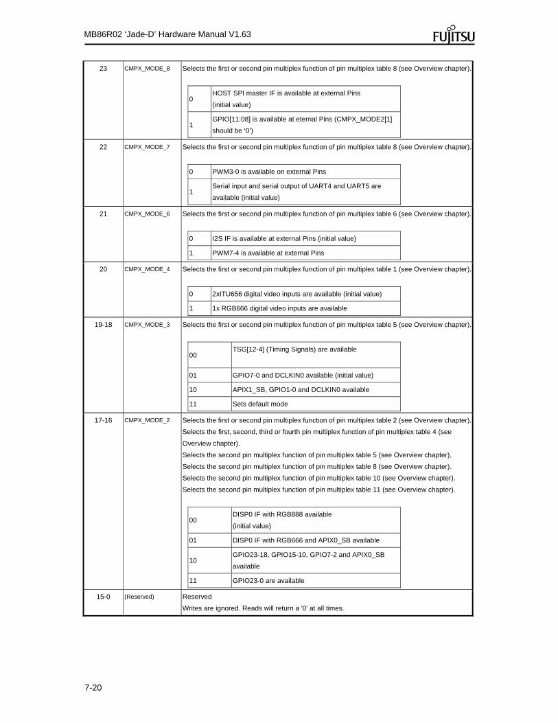
7-20
MB86R02 ‘Jade-D’ Hardware Manual V1.63
23 CMPX_MODE_8 Selects the first or second pin multiplex function of pin multiplex table 8 (see Overview chapter).
0 HOST SPI master IF is available at external Pins
(initial value)
1 GPIO[11:08] is available at eternal Pins (CMPX_MODE2[1]
should be ‘0’)
22 CMPX_MODE_7 Selects the first or second pin multiplex function of pin multiplex table 8 (see Overview chapter).
0 PWM3-0 is available on external Pins
1 Serial input and serial output of UART4 and UART5 are
available (initial value)
21 CMPX_MODE_6 Selects the first or second pin multiplex function of pin multiplex table 6 (see Overview chapter).
0 I2S IF is available at external Pins (initial value)
1 PWM7-4 is available at external Pins
20 CMPX_MODE_4 Selects the first or second pin multiplex function of pin multiplex table 1 (see Overview chapter).
0 2xITU656 digital video inputs are available (initial value)
1 1x RGB666 digital video inputs are available
19-18 CMPX_MODE_3 Selects the first or second pin multiplex function of pin multiplex table 5 (see Overview chapter).
00 TSG[12-4] (Timing Signals) are available
01 GPIO7-0 and DCLKIN0 available (initial value)
10 APIX1_SB, GPIO1-0 and DCLKIN0 available
11 Sets default mode
17-16 CMPX_MODE_2 Selects the first or second pin multiplex function of pin multiplex table 2 (see Overview chapter).
Selects the first, second, third or fourth pin multiplex function of pin multiplex table 4 (see
Overview chapter).
Selects the second pin multiplex function of pin multiplex table 5 (see Overview chapter).
Selects the second pin multiplex function of pin multiplex table 8 (see Overview chapter).
Selects the second pin multiplex function of pin multiplex table 10 (see Overview chapter).
Selects the second pin multiplex function of pin multiplex table 11 (see Overview chapter).
00 DISP0 IF with RGB888 available
(initial value)
01 DISP0 IF with RGB666 and APIX0_SB available
10 GPIO23-18, GPIO15-10, GPIO7-2 and APIX0_SB
available
11 GPIO23-0 are available
15-0 (Reserved) Reserved
Writes are ignored. Reads will return a '0' at all times.
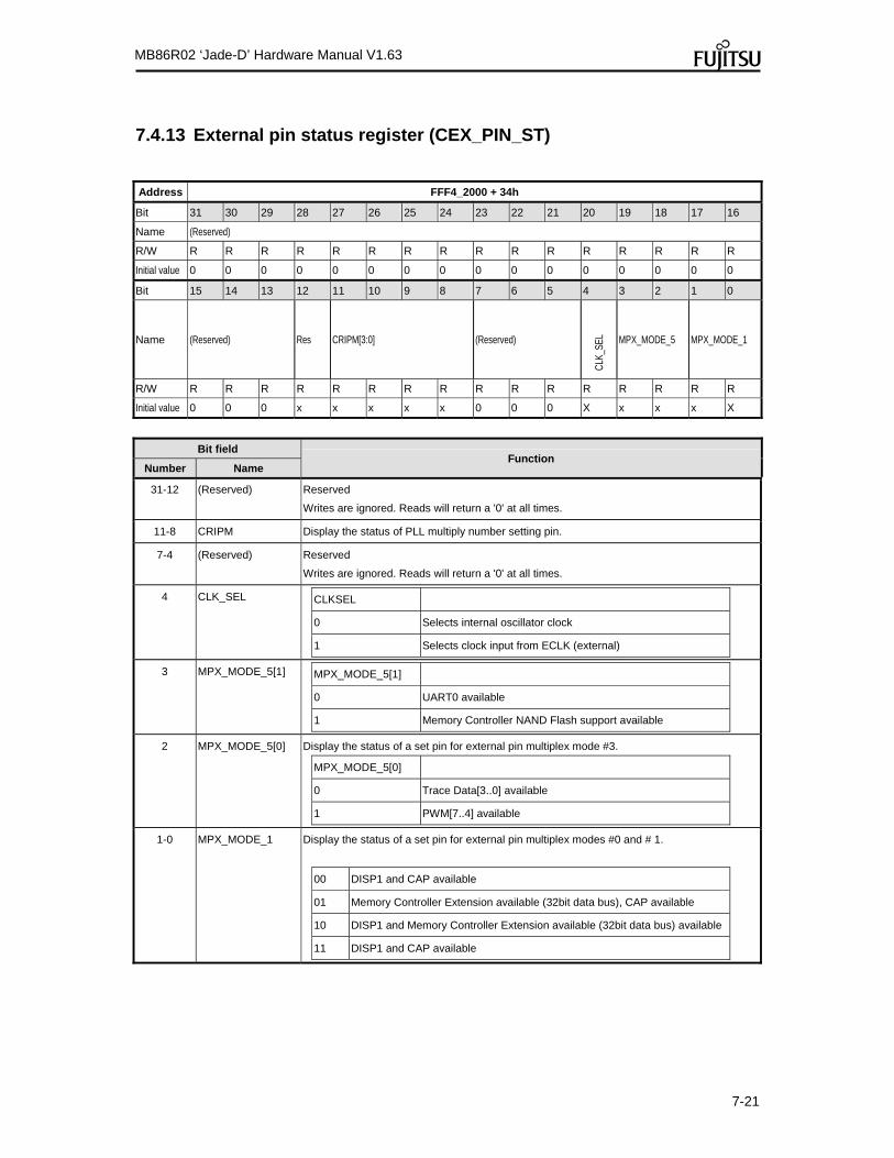
7-21
MB86R02 ‘Jade-D’ Hardware Manual V1.63
7.4.13 External pin status register (CEX_PIN_ST)
Address FFF4_2000 + 34h
Bit 31 30 29 28 27 26 25 24 23 22 21 20 19 18 17 16
Name (Reserved)
R/W R R R R R R R R R R R R R R R R
Initial value 0 0 0 0 0 0 0 0 0 0 0 0 0 0 0 0
Bit 15 14 13 12 11 10 9 8 7 6 5 4 3 2 1 0
Name (Reserved) Res CRIPM[3:0] (Reserved)
CLK_
SEL MPX_MODE_5 MPX_MODE_1
R/W R R R R R R R R R R R R R R R R
Initial value 0 0 0 x x x x x 0 0 0 X x x x X
Bit field Function
Number Name
31-12 (Reserved) Reserved
Writes are ignored. Reads will return a '0' at all times.
11-8 CRIPM Display the status of PLL multiply number setting pin.
7-4 (Reserved) Reserved
Writes are ignored. Reads will return a '0' at all times.
4 CLK_SEL
CLKSEL
0 Selects internal oscillator clock
1 Selects clock input from ECLK (external)
3 MPX_MODE_5[1]
MPX_MODE_5[1]
0 UART0 available
1 Memory Controller NAND Flash support available
2 MPX_MODE_5[0] Display the status of a set pin for external pin multiplex mode #3.
MPX_MODE_5[0]
0 Trace Data[3..0] available
1 PWM[7..4] available
1-0 MPX_MODE_1 Display the status of a set pin for external pin multiplex modes #0 and # 1.
00 DISP1 and CAP available
01 Memory Controller Extension available (32bit data bus), CAP available
10 DISP1 and Memory Controller Extension available (32bit data bus) available
11 DISP1 and CAP available

7-22
MB86R02 ‘Jade-D’ Hardware Manual V1.63
7.4.14 MediaLB set register (CMLB)
Address FFF4_2000 + 38h
Bit 31 30 29 28 27 26 25 24 23 22 21 20 19 18 17 16
Name (Reserved)
R/W R R R R R R R R R R R R R R R R
Initial value 0 0 0 0 0 0 0 0 0 0 0 0 0 0 0 0
Bit 15 14 13 12 11 10 9 8 7 6 5 4 3 2 1 0
Name (Reserved) SEL_SP
READ
R/W R R R R R R R R R R R R R R R R/W
Initial value 0 0 0 0 0 0 0 0 0 0 0 0 0 0 0 0
Bit field Function
Number Name
31-1 (Reserved) Reserved
Writes are ignored. Reads will return a '0' at all times.
0 SEL_SPREAD Switch the method of MediaLB of the AHB read data output.
0 CaseA (see below)
1 CaseB (see below)
Switch the method of MediaLB of the AHB read data output.
> case(A) . . . Output word data.
HRDATA
31-24 23-16 15-8 7-0
BigEndian Word 0h Byte0, Byte1, Byte2, Byte3
Half Word 0h Byte0, Byte1, Byte2, Byte3
Half Word 2h Byte0, Byte1, Byte2, Byte3
Byte 0h Byte0, Byte1, Byte2, Byte3
Byte 1h Byte0, Byte1, Byte2, Byte3
Byte 2h Byte0, Byte1, Byte2, Byte3
Byte 3h Byte0, Byte1, Byte2, Byte3
LittleEndian Word 0h Byte3, Byte2, Byte1, Byte0
Half Word 0h Byte3, Byte2, Byte1, Byte0
Half Word 2h Byte3, Byte2, Byte1, Byte0
Byte 0h Byte3, Byte2, Byte1, Byte0
Byte 1h Byte3, Byte2, Byte1, Byte0
Byte 2h Byte3, Byte2, Byte1, Byte0
Byte 3h Byte3, Byte2, Byte1, Byte0

7-23
MB86R02 ‘Jade-D’ Hardware Manual V1.63
> case(B) . . . sort by the valid data and output
HRDATA
31-24 23-16 15-8 7-0
BigEndian Word 0h Byte0, Byte1, Byte2, Byte3
Half Word 0h Byte0, Byte1, Byte0, Byte1
Half Word 2h Byte2, Byte3, Byte2, Byte3
Byte 0h Byte0, Byte0, Byte0, Byte0
Byte 1h Byte1, Byte1, Byte1, Byte1
Byte 2h Byte2, Byte2, Byte2, Byte2
Byte 3h Byte3, Byte3, Byte3, Byte3
LittleEndian Word 0h Byte3, Byte2, Byte1, Byte0
Half Word 0h Byte1, Byte0, Byte1, Byte0
Half Word 2h Byte3, Byte2, Byte3, Byte2
Byte 0h Byte0, Byte0, Byte0, Byte0
Byte 1h Byte1, Byte1, Byte1, Byte1
Byte 2h Byte2, Byte2, Byte2, Byte2
Byte 3h Byte3, Byte3, Byte3, Byte3

7-24
MB86R02 ‘Jade-D’ Hardware Manual V1.63
7.4.15 MBUS2AXU set register (CMBUS)
Address FFF4_2000 + 44h
Bit 31 30 29 28 27 26 25 24 23 22 21 20 19 18 17 16
Name (Reserved)
R/W R R R R R R R R R R R R R R R R
Initial value 0 0 0 0 0 0 0 0 0 0 0 0 0 0 0 0
Bit 15 14 13 12 11 10 9 8 7 6 5 4 3 2 1 0
Name (Reserved) WTWAIT RTWAIT FCAP[2:0]
R/W R R R R R R R R R R R R/W R/W R/W R/W R/W
Initial value 0 0 0 0 0 0 0 0 0 0 0 0 0 0 0 0
Bit field Function
Number Name
31-5 (Reserved) Reserved
Writes are ignored. Reads will return a '0' at all times.
4 DRAW_MBUS_WTWAIT Transaction wait setting for write transaction The next transaction is not begun until the
transaction is completed on an internal bus.
0 Don't wait
1 Wait
3 DRAW_MBUS_RTWAIT Transaction wait setting for read transaction The next transaction is not begun until the
transaction is completed on an internal bus.
0 Don't wait
1 Wait
2-0 DRAW_MBUS_FCAP Built-in FIFO steps number setting.
000 8 steps
001 1 step
010 2 steps
011 3 steps
100 4 steps
101 5 steps
110 6 steps
111 7 steps

7-25
MB86R02 ‘Jade-D’ Hardware Manual V1.63
7.4.16 Mode switch register like endian etc. (CBSC)
This register is for various mode switches. Set the endian switch as follows.
Address FFF4_2000 + E8h
Bit 31 30 29 28 27 26 25 24 23 22 21 20 19 18 17 16
Name (Reserved) *1 (Reserved) *2 (Reserved) SD_Endian[2:0] (Reserv
ed) I2S0_Endian[2:0]
R/W RW RW RW RW RW RW RW RW RW RW RW RW RW RW RW RW
Initial value 0 0 0 0 0 0 0 0 0 0 0 0 0 0 0 0
Bit 15 14 13 12 11 10 9 8 7 6 5 4 3 2 1 0
Name (Reserved) (Reserv
ed) (Reserved) (Reserved) (Reserved) (Reserved) *3 *4
R/W RW RW RW RW RW RW RW RW RW RW RW RW RW RW RW RW
Initial value 0 0 0 0 0 0 0 0 0 0 0 0 0 0 0 0
*3: VideoCap_performance
*4: AHB2AXI_BIGMODE
Bit field Function
Number Name
31 (Reserved) Reserved
Writes are ignored. Reads will return a '0' at all times.
30-28 (Reserved)
27 (Reserved) Reserved
Writes are ignored. Reads will return a '0' at all times.
26-24 (Reserved)
23 (Reserved) Reserved
Writes are ignored. Reads will return a '0' at all times.
22-20 SD_Endian The Endian switch of SD is controlled.
Bit 22 wSEL Endian switch 0: Little 1:Big
Bit 21 HWSAP Hword byte swap switch signal at Big
Bit 20 WSWAP Word byte swap switch signal at Big
19 (Reserved) Reserved
Writes are ignored. Reads will return a '0' at all times.
18-16 I2S0_Endian The Endian switch of I2S0 is controlled.
wSEL 0 (Little)
1 (Big)
Note that only 32 bit access is possible to DDR
memory in big endian mode
HWSWAP - (There is no SWAP. ) 0 (There is Swap. ) 1(There is no Swap. )
WSWAP - (There is no SWAP. ) 0 (There is Swap. ) 1(There is no Swap. )
WSEL:Little/Big switch signal
Hword byte swap switch signal at HWSWAP:Big
Word byte swap switch signal at WSWAP:Big

7-26
MB86R02 ‘Jade-D’ Hardware Manual V1.63
Bit field Function
Number Name
Bit 18 wSEL Endian switch 0: Little 1:Big
Bit 17 HWSAP Hword byte swap switch signal at Big
Bit 16 WSWAP Word byte swap switch signal at Big
15 (Reserved) Reserved
Writes are ignored. Reads will return a '0' at all times.
14-12 (Reserved)
11 (Reserved) Reserved
Writes are ignored. Reads will return a '0' at all times.
10-8 (Reserved)
7 (Reserved) Reserved
Writes are ignored. Reads will return a '0' at all times.
6-4 (Reserved)
3-2 (Reserved) Reserved
Writes are ignored. Reads will return a '0' at all times.
1 VideoCap_performa
nce
Do video capture performance improvement EC valid.
0 Before measures of EC (initial value)
1 After measures of EC
0 AHB2AXI_BIGMOD
E
Toggle control signal “BIGMODE" for the big endian of the AHB2AXI module is controlled.
0 After for EC (initial value)
1 Ahead for EC
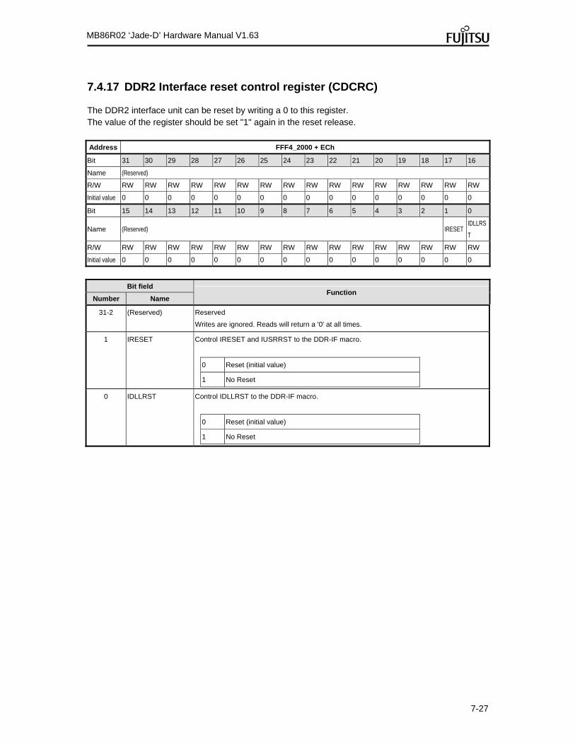
7-27
MB86R02 ‘Jade-D’ Hardware Manual V1.63
7.4.17 DDR2 Interface reset control register (CDCRC)
The DDR2 interface unit can be reset by writing a 0 to this register. The value of the register should be set "1" again in the reset release.
Address FFF4_2000 + ECh
Bit 31 30 29 28 27 26 25 24 23 22 21 20 19 18 17 16
Name (Reserved)
R/W RW RW RW RW RW RW RW RW RW RW RW RW RW RW RW RW
Initial value 0 0 0 0 0 0 0 0 0 0 0 0 0 0 0 0
Bit 15 14 13 12 11 10 9 8 7 6 5 4 3 2 1 0
Name (Reserved) IRESETIDLLRS
T
R/W RW RW RW RW RW RW RW RW RW RW RW RW RW RW RW RW
Initial value 0 0 0 0 0 0 0 0 0 0 0 0 0 0 0 0
Bit field Function
Number Name
31-2 (Reserved) Reserved
Writes are ignored. Reads will return a '0' at all times.
1 IRESET Control IRESET and IUSRRST to the DDR-IF macro.
0 Reset (initial value)
1 No Reset
0 IDLLRST Control IDLLRST to the DDR-IF macro.
0 Reset (initial value)
1 No Reset
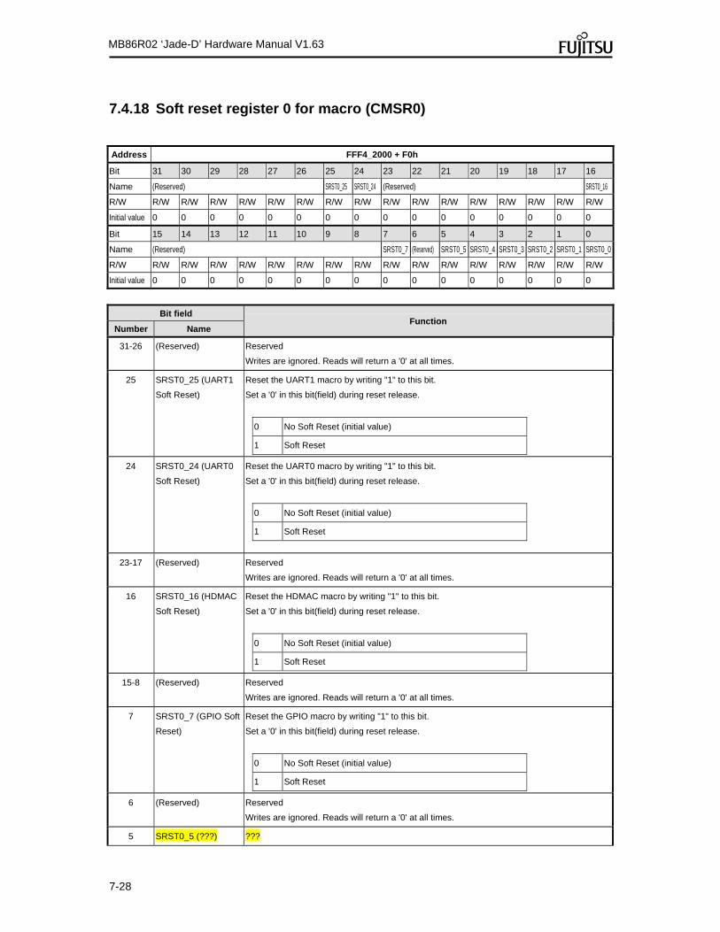
7-28
MB86R02 ‘Jade-D’ Hardware Manual V1.63
7.4.18 Soft reset register 0 for macro (CMSR0)
Address FFF4_2000 + F0h
Bit 31 30 29 28 27 26 25 24 23 22 21 20 19 18 17 16
Name (Reserved) SRST0_25 SRST0_24 (Reserved) SRST0_16
R/W R/W R/W R/W R/W R/W R/W R/W R/W R/W R/W R/W R/W R/W R/W R/W R/W
Initial value 0 0 0 0 0 0 0 0 0 0 0 0 0 0 0 0
Bit 15 14 13 12 11 10 9 8 7 6 5 4 3 2 1 0
Name (Reserved) SRST0_7 (Reserved) SRST0_5 SRST0_4 SRST0_3 SRST0_2 SRST0_1 SRST0_0
R/W R/W R/W R/W R/W R/W R/W R/W R/W R/W R/W R/W R/W R/W R/W R/W R/W
Initial value 0 0 0 0 0 0 0 0 0 0 0 0 0 0 0 0
Bit field Function
Number Name
31-26 (Reserved) Reserved
Writes are ignored. Reads will return a '0' at all times.
25 SRST0_25 (UART1
Soft Reset)
Reset the UART1 macro by writing "1" to this bit.
Set a '0' in this bit(field) during reset release.
0 No Soft Reset (initial value)
1 Soft Reset
24 SRST0_24 (UART0
Soft Reset)
Reset the UART0 macro by writing "1" to this bit.
Set a '0' in this bit(field) during reset release.
0 No Soft Reset (initial value)
1 Soft Reset
23-17 (Reserved) Reserved
Writes are ignored. Reads will return a '0' at all times.
16 SRST0_16 (HDMAC
Soft Reset)
Reset the HDMAC macro by writing "1" to this bit.
Set a '0' in this bit(field) during reset release.
0 No Soft Reset (initial value)
1 Soft Reset
15-8 (Reserved) Reserved
Writes are ignored. Reads will return a '0' at all times.
7 SRST0_7 (GPIO Soft
Reset)
Reset the GPIO macro by writing "1" to this bit.
Set a '0' in this bit(field) during reset release.
0 No Soft Reset (initial value)
1 Soft Reset
6 (Reserved) Reserved
Writes are ignored. Reads will return a '0' at all times.
5 SRST0_5 (???) ???

7-29
MB86R02 ‘Jade-D’ Hardware Manual V1.63
Bit field Function
Number Name
4 SRST0_4 (GDC
DISP1 Soft Reset)
Reset the GDC DISP1 macro by writing "1" to this bit.
Set a '0' in this bit(field) during reset release.
0 No Soft Reset (initial value)
1 Soft Reset
3 SRST0_3 (GDC
DISP0 Soft Reset)
Reset the HDMAC macro by writing "1" to this bit.
Set a '0' in this bit(field) during reset release.
0 No Soft Reset (initial value)
1 Soft Reset
2 SRST0_2 (GDC
CAP1 Soft Reset)
Reset the GDC CAP1 macro by writing "1" to this bit.
Set a '0' in this bit(field) during reset release.
0 No Soft Reset (initial value)
1 Soft Reset
1 SRST0_1 (GDC
CAP0 Soft Reset)
Reset the GDC CAP0 macro by writing "1" to this bit.
Set a '0' in this bit(field) during reset release.
0 No Soft Reset (initial value)
1 Soft Reset
0 SRST0_0 (GDC Draw
Soft Reset)
Reset the GDC Draw macro by writing "1" to this bit.
Set a '0' in this bit(field) during reset release.
0 No Soft Reset (initial value)
1 Soft Reset

7-30
MB86R02 ‘Jade-D’ Hardware Manual V1.63
7.4.19 Soft reset register 1 for macro (CMSR1)
Address FFF4_2000 + F4h
Bit 31 30 29 28 27 26 25 24 23 22 21 20 19 18 17 16
Name SRST1_31 SRST1_30 SRST1_29 SRST1_28 SRST1_27 SRST1_26 SRST1_25 SRST0_2
4 Res Res Res Res Res SRST1_18 SRST1_17 SRST1_16
R/W R R R R/W R/W R/W R/W R/W R R R R R R R/W R/W
Initial value 0 0 0 0 0 0 0 0 0 0 0 0 0 0 0 0
Bit 15 14 13 12 11 10 9 8 7 6 5 4 3 2 1 0
Name SRST1_15 SRST1_14 SRST1_13 SRST1_12 SRST1_11 Res SRST1_9 Res Res SRST1_6 SRST1_5 SRST1_4 SRST1_3 SRST1_2 SRST1_1 SRST1_0
R/W R/W R/W R/W R/W R/W R R/W R R R/W R/W R/W R/W R/W R/W R/W
Initial value 0 0 0 0 0 0 0 0 0 0 0 0 0 0 0 0
Bit field Function
Number Name
31 SRST1_31 (GPIO
Soft Reset)
Reset the GPIO macro by writing "1" to this bit.
Set a '0' in this bit(field) during reset release.
0 No Soft Reset (initial value)
1 Soft Reset
30 SRST1_30 (AXI
Soft Reset)
Do the output of reset to (AXI macro by writing "1" to this bit.
Set a '0' in this bit(field) during reset release.
0 No Soft Reset (initial value)
1 Soft Reset
29 SRST1_29
(MediaLB Soft
Reset)
Do the output of reset to (MediaLB macro by writing "1" to this bit.
Set a '0' in this bit(field) during reset release.
0 No Soft Reset (initial value)
1 Soft Reset
28 SRST1_28
(HBUS2AXI Soft
Reset)
Reset the HBUS2AXI macro by writing "1" to this bit. Set a '0' in this bit(field) during reset
release.
0 No Soft Reset (initial value)
1 Soft Reset
27 SRST1_27
(MBUS2AXI(Draw)
Soft Reset)
Reset the MBUS2AXI(Draw) macro by writing "1" to this bit. Set a '0' in this bit(field) during reset
release.
0 No Soft Reset (initial value)
1 Soft Reset

7-31
MB86R02 ‘Jade-D’ Hardware Manual V1.63
Bit field Function
Number Name
26 SRST1_26
(MBUS2AXI(DispCa
p) Soft Reset)
Reset the MBUS2AXI(DispCap) macro by writing "1" to this bit. Set a '0' in this bit(field) during
reset release.
0 No Soft Reset (initial value)
1 Soft Reset
25 SRST1_25
(AHB2AXI(CPUroot)
Soft Reset)
Reset the AHB2AXI(CPUroot) macro by writing "1" to this bit. Set a '0' in this bit(field) during
reset release.
0 No Soft Reset (initial value)
1 Soft Reset
24 SRST1_24
(AHB2AXI(AHBBus)
Soft Reset)
Reset the AHB2AXI(AHBBus) macro by writing "1" to this bit. Set a '0' in this bit(field) during reset
release.
0 No Soft Reset (initial value)
1 Soft Reset
23 - 19 (Reserved)
18 SRST1_18 (UART5
Soft Reset)
Reset the UART5 macro by writing "1" to this bit.
Set a '0' in this bit(field) during reset release.
0 No Soft Reset (initial value)
1 Soft Reset
17 SRST1_17 (UART4
Soft Reset)
Reset the UART4 macro by writing "1" to this bit.
Set a '0' in this bit(field) during reset release.
0 No Soft Reset (initial value)
1 Soft Reset
16 SRST1_16 (UART3
Soft Reset)
Reset the UART3 macro by writing "1" to this bit.
Set a '0' in this bit(field) during reset release.
0 No Soft Reset (initial value)
1 Soft Reset
15 SRST1_15 (UART2
Soft Reset)
Reset the UART2 macro by writing "1" to this bit.
Set a '0' in this bit(field) during reset release.
0 No Soft Reset (initial value)
1 Soft Reset
14 SRST1_14 (PWM_1
Soft Reset)
Reset the PWM_1 macro by writing "1" to this bit.
Set a '0' in this bit(field) during reset release.
0(h) No Soft Reset (initial value)
1(h) Soft Reset
7-32
MB86R02 ‘Jade-D’ Hardware Manual V1.63
Bit field Function
Number Name
13 SRST1_13 (PWM_0
Soft Reset)
Reset the PWM_0 macro by writing "1" to this bit.
Set a '0' in this bit(field) during reset release.
0 No Soft Reset (initial value)
1 Soft Reset
12 SRST1_12 (I2C_0
Soft Reset)
Reset the I2C_0 macro by writing "1" to this bit.
Set a '0' in this bit(field) during reset release.
0(h) No Soft Reset (initial value)
1(h) Soft Reset
11 SRST1_11 (I2C_0
Soft Reset)
Reset the I2C_0 macro by writing "1" to this bit.
Set a '0' in this bit(field) during reset release.
0 No Soft Reset (initial value)
1 Soft Reset
10 (Reserved)
9 SRST1_9 (SPI Soft
Reset)
Reset the SPI macro by writing "1" to this bit.
Set a '0' in this bit(field) during reset release.
0 No Soft Reset (initial value)
1 Soft Reset
8 - 7 (Reserved)
6 SRST1_6 (I2S_0
Soft Reset)
Reset the I2S_0 macro by writing "1" to this bit.
Set a '0' in this bit(field) during reset release.
0 No Soft Reset (initial value)
1 Soft Reset
5 SRST1_5
(MBUS2AXI(Cap))
Reset the MBUS2AXI(Cap) macro by writing "1" to this bit. Set a '0' in this bit(field) during reset
release.
0 No Soft Reset (initial value)
1 Soft Reset
4 SRST1_4 (SD i/f
Soft Reset)
Reset the SD i/f macro by writing "1" to this bit.
Set a '0' in this bit(field) during reset release.
0 No Soft Reset (initial value)
1 Soft Reset
3 SRST1_3 (CAN1
Soft Reset)
Reset the CAN1 macro by writing "1" to this bit.
Set a '0' in this bit(field) during reset release.
0 No Soft Reset (initial value)
1 Soft Reset

7-33
MB86R02 ‘Jade-D’ Hardware Manual V1.63
Bit field Function
Number Name
2 SRST1_2 (CAN0
Soft Reset)
Reset the CAN0 macro by writing "1" to this bit.
Set a '0' in this bit(field) during reset release.
0 No Soft Reset (initial value)
1 Soft Reset
1 SRST1_1 (DDR2
Soft Reset)
Reset the DDR2 controller macro by writing "1" to this bit. Set a '0' in this bit(field) during reset
release.
0 No Soft Reset (initial value)
1 Soft Reset
0 SRST1_0 (GDC
Soft Reset)
Reset the GDC macro by writing "1" to this bit.
Set a '0' in this bit(field) during reset release.
0 No Soft Reset (initial value)
1 Soft Reset
7.4.20 Soft reset register 2 for macro (CMSR2)
Address FFF2_2000 + F8h
Bit 31 30 29 28 27 26 25 24 23 22 21 20 19 18 17 16
Name (Reserved)
R/W R R R R/W R/W R/W R/W R/W R/W R/W R/W R/W R/W R/W R/W R/W
Initial value 0 0 0 0 0 0 0 0 0 0 0 0 0 0 0 0
Bit 15 14 13 12 11 10 9 8 7 6 5 4 3 2 1 0
Name (Reserv
ed) SRST2_14 SRST2_13 SRST2_12 SRST2_11 SRST2_10 SRST2_9 SRST2_8 SRST2_7 SRST2_6 SRST2_5 SRST2_4 SRST2_3 SRST2_2 SRST2_1 SRST2_0
R/W R/W R/W R/W R/W R/W R/W R/W R/W R/W R/W R/W R/W R/W R/W R/W R/W
Initial value 0 0 0 0 0 0 0 0 0 0 0 0 0 0 0 0
Bit field Function
Number Name
31-9 (Reserved) Reserved
Writes are ignored. Reads will return a '0' at all times.
14 SRST2_14
(DPERI1 Soft
Reset)
Reset the DPERI1 macro by writing "1" to this bit.
Set a '0' in this bit(field) during reset release.
0 No Soft Reset (initial value)
1 Soft Reset

7-34
MB86R02 ‘Jade-D’ Hardware Manual V1.63
Bit field Function
Number Name
13 SRST2_13
(DPERI0 Soft
Reset)
Do the output of reset to DPERI0 macro by writing "1" to this bit.
Set a '0' in this bit(field) during reset release.
0 No Soft Reset (initial value)
1 Soft Reset
12 SRST2_12 (RLD2
Soft Reset)
Reset the RLD macro by writing "1" to this bit.
Set a '0' in this bit(field) during reset release.
0 No Soft Reset (initial value)
1 Soft Reset
11 SRST2_11
(APIXch1 Soft
Reset)
Reset the APIX ch1 (incl PHY, Ashell, RegIf) macro by writing "1" to this bit.
Set a '0' in this bit(field) during reset release.
0 No Soft Reset (initial value)
1 Soft Reset
10 SRST2_10
(APIXch0 Soft
Reset)
Reset the APIX ch0 (incl PHY, Ashell, RegIf) macro by writing "1" to this bit.
Set a '0' in this bit(field) during reset release.
0 No Soft Reset (initial value)
1 Soft Reset
9 SRST2_9 (ADC Soft
Reset)
Reset the ADC macro by writing "1" to this bit.
Set a '0' in this bit(field) during reset release.
0 No Soft Reset (initial value)
1 Soft Reset
8 SRST2_8 (PWM_7
Soft Reset)
Reset the PWM_7 macro by writing "1" to this bit.
Set a '0' in this bit(field) during reset release.
0 No Soft Reset (initial value)
1 Soft Reset
7 SRST2_7 (PWM_6
Soft Reset)
Reset the PWM_6 macro by writing "1" to this bit.
Set a '0' in this bit(field) during reset release.
0 No Soft Reset (initial value)
1 Soft Reset
6 SRST2_6 (PWM_5
Soft Reset)
Reset the PWM_5 macro by writing "1" to this bit.
Set a '0' in this bit(field) during reset release.
0 No Soft Reset (initial value)
1 Soft Reset

7-35
MB86R02 ‘Jade-D’ Hardware Manual V1.63
Bit field Function
Number Name
5 SRST2_5 (PWM_4
Soft Reset)
Reset the PWM_4 macro by writing "1" to this bit.
Set a '0' in this bit(field) during reset release.
0 No Soft Reset (initial value)
1 Soft Reset
4 SRST2_4 (PWM_3
Soft Reset)
Reset the PWM_3 macro by writing "1" to this bit.
Set a '0' in this bit(field) during reset release.
0 No Soft Reset (initial value)
1 Soft Reset
3 SRST2_3 (PWM_2
Soft Reset)
Reset the PWM_2 macro by writing "1" to this bit.
Set a '0' in this bit(field) during reset release.
0 No Soft Reset (initial value)
1 Soft Reset
2 SRST2_2 (I2C_1
Soft Reset)
Reset the I2C_1 macro by writing "1" to this bit.
Set a '0' in this bit(field) during reset release.
0 No Soft Reset (initial value)
1 Soft Reset
1 SRST2_1
(HOST_SPI Soft
Reset)
Reset the HOST_SPI macro by writing "1" to this bit.
Set a '0' in this bit(field) during reset release.
0 No Soft Reset (initial value)
1 Soft Reset
0 SRST2_0 (SPI1
Soft Reset)
Reset the SPI1 macro by writing "1" to this bit.
Set a '0' in this bit(field) during reset release.
0 No Soft Reset (initial value)
1 Soft Reset
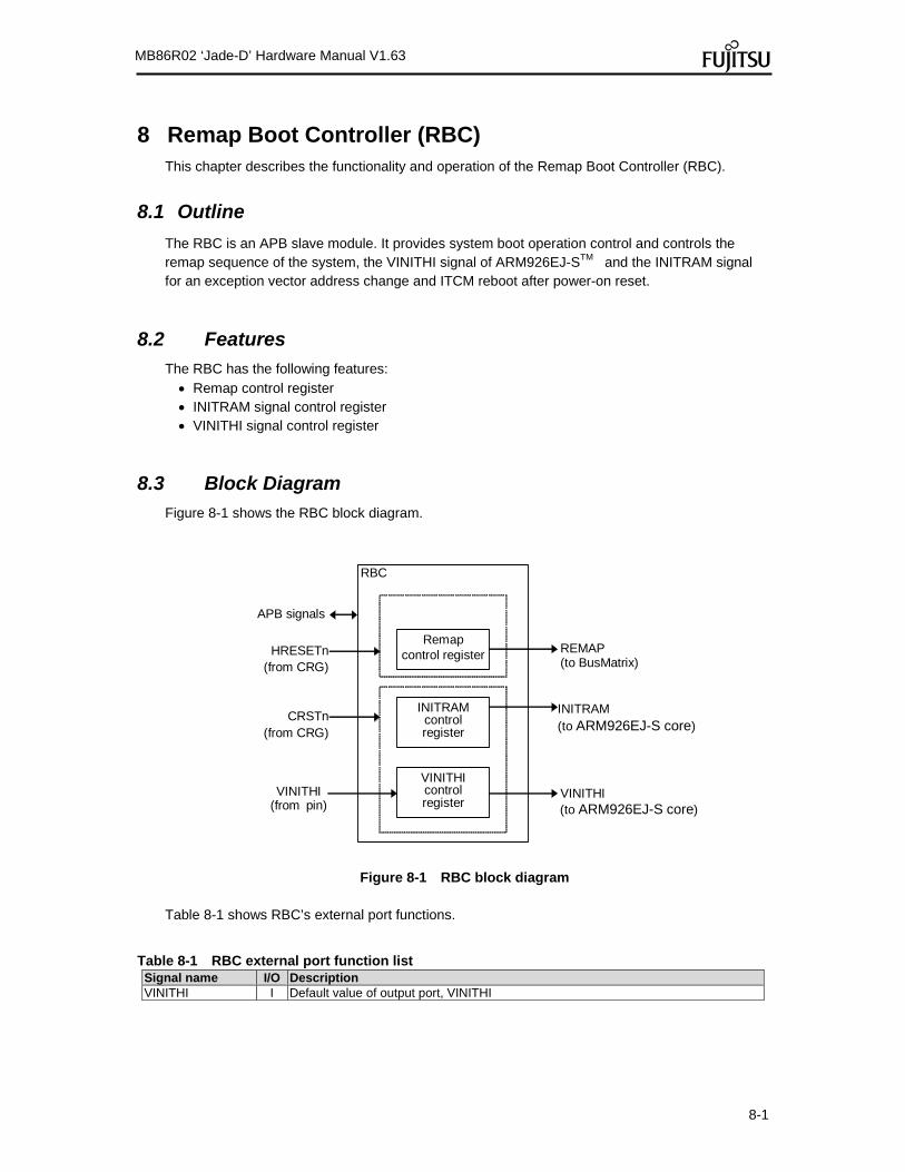
8-1
MB86R02 ‘Jade-D’ Hardware Manual V1.63
8 Remap Boot Controller (RBC) This chapter describes the functionality and operation of the Remap Boot Controller (RBC).
8.1 Outline
The RBC is an APB slave module. It provides system boot operation control and controls the remap sequence of the system, the VINITHI signal of ARM926EJ-STM and the INITRAM signal for an exception vector address change and ITCM reboot after power-on reset.
8.2 Features
The RBC has the following features: Remap control register INITRAM signal control register VINITHI signal control register
8.3 Block Diagram
Figure 8-1 shows the RBC block diagram.
RBC
Remap control register
APB signals
REMAP
INITRAMcontrol register
INITRAM
VINITHIcontrol register
VINITHI (from pin)
VINITHI
CRSTn (from CRG)
HRESETn (from CRG) (to BusMatrix)
(to ARM926EJ-S core)
(to ARM926EJ-S core)
Figure 8-1 RBC block diagram Table 8-1 shows RBC’s external port functions.
Table 8-1 RBC external port function list Signal name I/O Description VINITHI I Default value of output port, VINITHI

8-2
MB86R02 ‘Jade-D’ Hardware Manual V1.63
8.4 Supply clock
The APB clock is supplied to the RBC. Please refer to the chapter Clock Reset Generator (CRG) for details about frequency setting and control of the clock.
8.5 Register
This section describes the RBC registers.
8.5.1 Register list
The RBC is controlled by the registers shown in Table 8-2.
Table 8-2 RBC register list Address
Register name Abbreviation Description Base Offset
FFFE_6000H + 00H (Reserved) – Reserved area (access prohibited)
+ 04H Remap control register RBREMAP Remap state control
+ 08H VINITHI control register A RBVIHA VINITHI output signal control
+ 0CH INITRAM control register A RBITRA INITRAM output signal control
+ 10H – + FFFH
(Reserved) – Reserved area (access prohibited)

8-3
MB86R02 ‘Jade-D’ Hardware Manual V1.63
Description format of register Following format is used for description of register’s each bit in "8.5.2 Remap control register (RBREMAP)" to "8.5.4 INITRAM control register A (RBITRA)".
Address Base address + Offset Bit 31 30 29 28 27 26 25 24 23 22 21 20 19 18 17 16
Name R/W
Initial value Bit 15 14 13 12 11 10 9 8 7 6 5 4 3 2 1 0
Name R/W
Initial value
Meaning of item and sign Address
Address (base address + offset address) of the register Bit
Bit number of the register Name
Bit field name of the register R/W
Attribution of read/write of each bit field R0:Read value is always "0" R1: Read value is always "1" W0: Write value is always "0", and write access of "1" is ignored W1: Write value is always "1", and write access of "0" is ignored R: Read W: Write Initial value
Each bit field’s value after reset 0: Value is "0" 1: Value is "1" X: Value is undefined
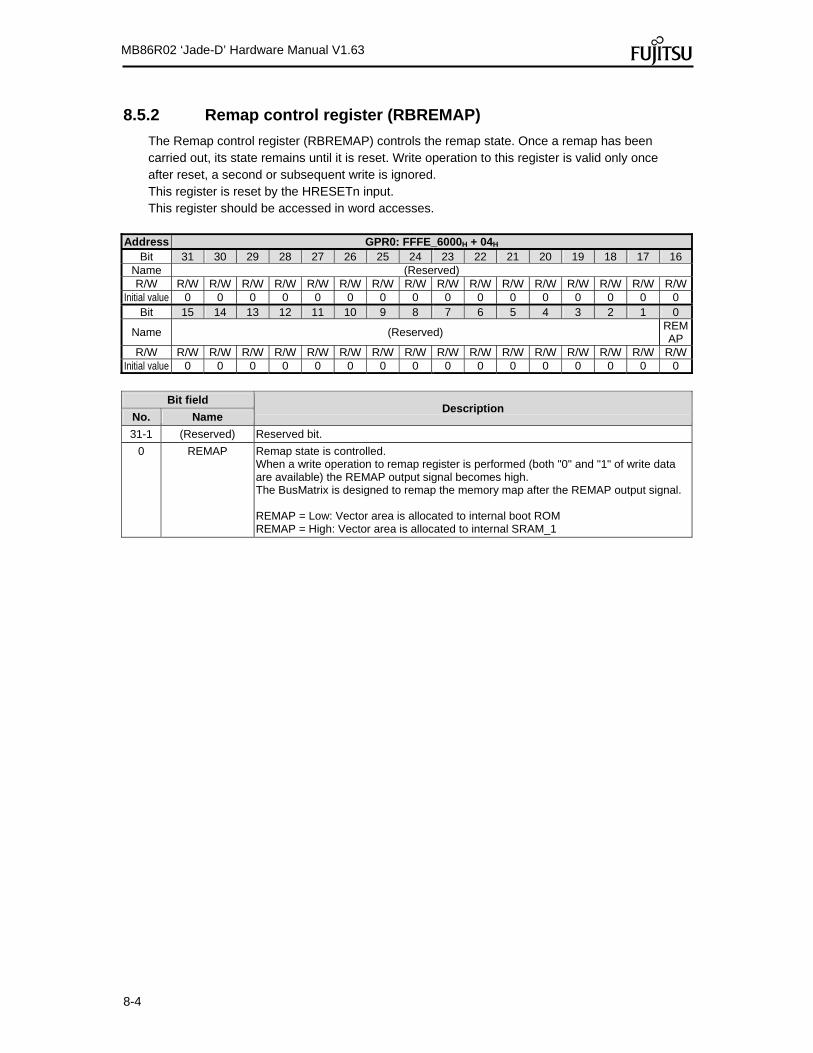
8-4
MB86R02 ‘Jade-D’ Hardware Manual V1.63
8.5.2 Remap control register (RBREMAP)
The Remap control register (RBREMAP) controls the remap state. Once a remap has been carried out, its state remains until it is reset. Write operation to this register is valid only once after reset, a second or subsequent write is ignored. This register is reset by the HRESETn input. This register should be accessed in word accesses.
Address GPR0: FFFE_6000H + 04H Bit 31 30 29 28 27 26 25 24 23 22 21 20 19 18 17 16
Name (Reserved) R/W R/W R/W R/W R/W R/W R/W R/W R/W R/W R/W R/W R/W R/W R/W R/W R/W
Initial value 0 0 0 0 0 0 0 0 0 0 0 0 0 0 0 0 Bit 15 14 13 12 11 10 9 8 7 6 5 4 3 2 1 0
Name (Reserved) REMAP
R/W R/W R/W R/W R/W R/W R/W R/W R/W R/W R/W R/W R/W R/W R/W R/W R/WInitial value 0 0 0 0 0 0 0 0 0 0 0 0 0 0 0 0
Bit field
Description No. Name
31-1 (Reserved) Reserved bit.
0 REMAP Remap state is controlled. When a write operation to remap register is performed (both "0" and "1" of write data are available) the REMAP output signal becomes high. The BusMatrix is designed to remap the memory map after the REMAP output signal. REMAP = Low: Vector area is allocated to internal boot ROM REMAP = High: Vector area is allocated to internal SRAM_1

8-5
MB86R02 ‘Jade-D’ Hardware Manual V1.63
8.5.3 VINITHI control register A (RBVIHA)
The VINITHI control register A (RBVIHA) controls the VINITHI output signal. This register is reset by the CRSTn input and its initial value is determined by the input level of the external pin VINITHI. This register should be accessed in word accesses.
Address GPR0: FFFE_6000H + 08H
Bit 31 30 29 28 27 26 25 24 23 22 21 20 19 18 17 16 Name (Reserved) R/W R R R R R R R R R R R R R R R R
Initial value Determined by input level of external pin, VINITHI Bit 15 14 13 12 11 10 9 8 7 6 5 4 3 2 1 0
Name (Reserved) VIHAR/W R R R R R R R R R R R R R R R R/W
Initial value Determined by input level of external pin, VINITHI
Bit field
Description No. Name
31-1 (Reserved) Reserved bits. Write access is ignored. Reading these bits enable reading the value set by VINITHI.
0 VIHA VINTHI output signal is controlled.
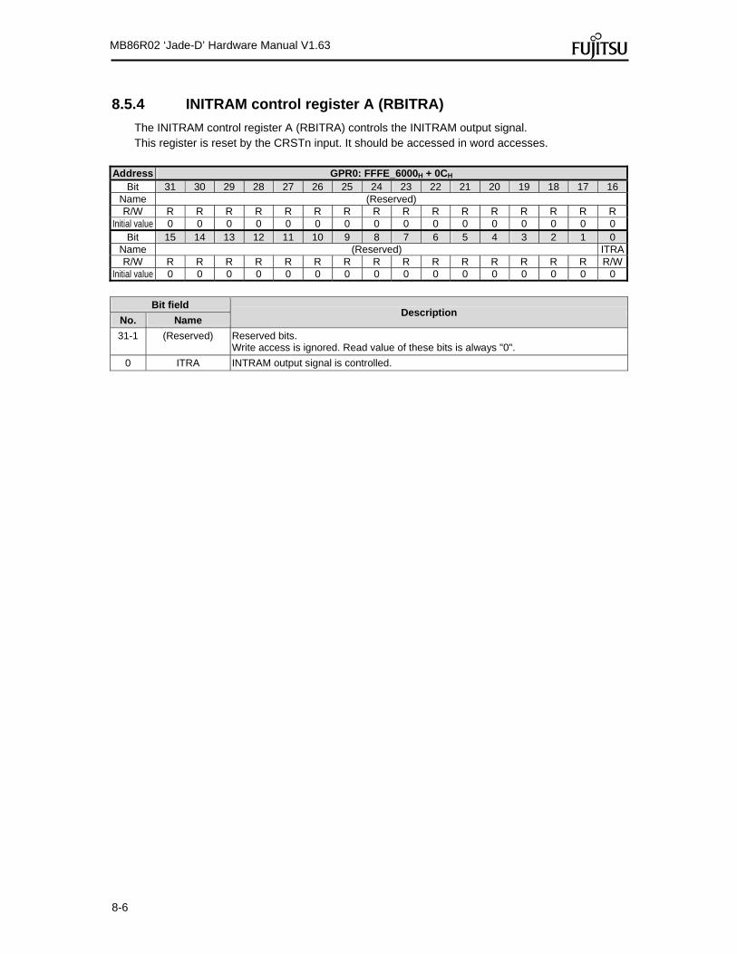
8-6
MB86R02 ‘Jade-D’ Hardware Manual V1.63
8.5.4 INITRAM control register A (RBITRA)
The INITRAM control register A (RBITRA) controls the INITRAM output signal. This register is reset by the CRSTn input. It should be accessed in word accesses.
Address GPR0: FFFE_6000H + 0CH Bit 31 30 29 28 27 26 25 24 23 22 21 20 19 18 17 16
Name (Reserved) R/W R R R R R R R R R R R R R R R R
Initial value 0 0 0 0 0 0 0 0 0 0 0 0 0 0 0 0 Bit 15 14 13 12 11 10 9 8 7 6 5 4 3 2 1 0
Name (Reserved) ITRAR/W R R R R R R R R R R R R R R R R/W
Initial value 0 0 0 0 0 0 0 0 0 0 0 0 0 0 0 0
Bit field
Description No. Name
31-1 (Reserved) Reserved bits. Write access is ignored. Read value of these bits is always "0".
0 ITRA INTRAM output signal is controlled.

8-7
MB86R02 ‘Jade-D’ Hardware Manual V1.63
8.6 Operation
This section describes the RBC's operation.
8.6.1 RBC reset
The RBC has two reset input ports. The RBREMAP register is reset by the HRESETn input and RBVIHA and RBITRA registers are reset by the CRSTn value. Table 8-3 shows the correlation between these resets and registers.
Table 8-3 Correlation between reset and register Reset input Register Description
HRESETn RBREMAP This port is reset by HRESETn.
CRSTn RBVIHA This port value reflects to value of external pin, VINITHI by CRSTn. input.
RBITRA This port is reset by CRSTn input.
8.6.2 Remap control
A remap changes the vector area (00000000H~00008000H) after power-on. The vector area is allocated to the built-in boot ROM at power-on and the system starts from it. Using the remap control, the allocated area is changed to the built-in SRAM_1 memory allowing the built-in vector table to be effectively overwritten.
8.6.3 VINITHI control
The ARM926EJ-S core has a VINITHI signal which determines the exception vector address. When low at reset, the exception vector is located at 00000000H. When the signal is high at reset, the exception vector is located in FFFF0000H. Refer to the "Technical reference manual" of ARM9 provided by ARM Ltd. for details about the VINITHI signal. The initial value of the RBVIHA register is defined by the external pin, VINITHI. Limitation: If VINITHI is high, then exception vectors have to be stored at physical address (00000000H~
00008000H). It is not possible to simultaneously use this with a remapped vector area to SRAM_1. (VINITHI =1 in conjunction with REMAP=1 is not allowed)
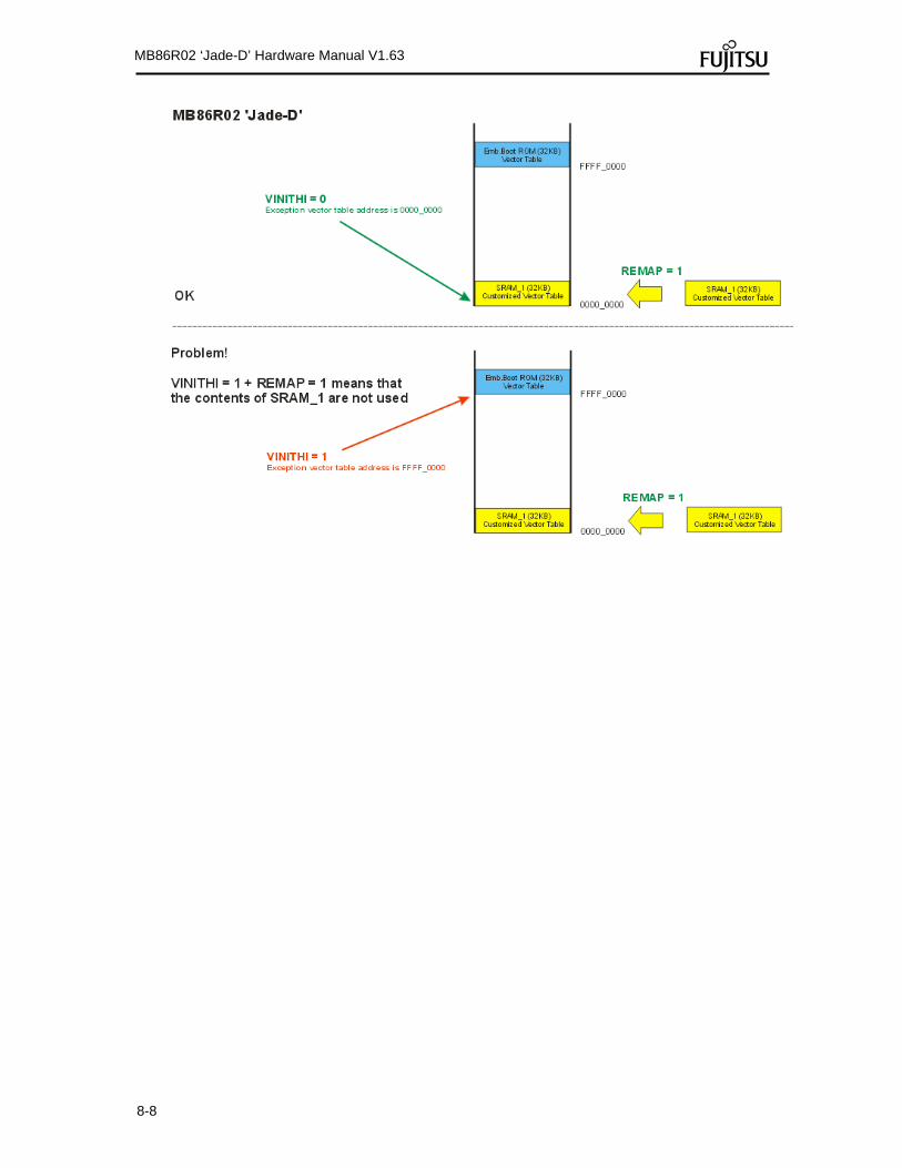
8-8
MB86R02 ‘Jade-D’ Hardware Manual V1.63

8-9
MB86R02 ‘Jade-D’ Hardware Manual V1.63
8.6.4 INITRAM control
The ARM926EJ-S core has an INITRAM signal. When high at reset, the instruction TCM automatically becomes valid which enables a reboot operation from ITCM. Refer to the "Technical reference manual" of the ARM9 core provided by ARM Ltd. for details of the INITRAM signal. The RBITRA register is initialized to "0" by CRSTn, however it is not reset by HRESETn. This means a reboot operation from ITCM can be executed at software reset if the exception vector table is copied to ITCM before a software reset.

9-1
MB86R02 ‘Jade-D’ Hardware Manual V1.63
9 Interrupt Request Controller (IRC) This chapter explains the interrupt controller's function and operation.
9.1 Overview
IRC is composed of three channels (IRC0, IRC1 and IRC2). IRC0/1/2 decides the priority of the IRQ source up to 32 factors respectively, and notifies the ARM core the IRQ source with the highest priority as IRQ interrupt. Therefore, IRC0/1/2 has a set register of the interrupt level permitted from a set register and the ARM core of the priority of the IRQ factor. Note: The IRQ interrupt decided by IRC1 is accepted as an interrupt factor of IRQ6 of IRC0. Therefore, the priority is decided by setting of IRC1 and setting IRQ6 of IRC0 as for all IRQ sources allocated in IRC1. Note: The IRQ interrupt decided by IRC2 is accepted as an interrupt factor of IRQ5 of IRC0. Therefore, the priority is decided by setting of IRC2 and setting IRQ5 of IRC0 as for all IRQ sources allocated in IRC2. As for the IRQ vector defined in ARM926EJ-S, the factor of the vector table can certain the expansion to 32 by IRC though only "0×18". When the IRQ interrupt is asserted to the ARM core, the address of the interrupt vector table corresponding to the IRQ interrupt factor is generated during the register, and displayed. The IRQ interrupt handler should refer from "0×18" to the vector table of the expansion that was able to be certained further. There is FIQ by the source and is no preference circuit for one. For the interrupt controller, the timing of the FIQ factor is controlled, and the attribute is transmitted to the ARM core as nFIQ assert. In addition, the interrupt controller provides with the delay interruption controller and the HOLD request cancellation demand circuit, and provides with the interrupt wake up circuit from stop/sleep mode composed of the clock control circuit. The interrupt controller is connected with the APB bus.
9.2 Features
The interrupt controller has the following features. It is 3 channels built-in as for IRC that can correspond to the interrupt request up to 32 factors. IRQ interrupt priority is decided, and it transmits to ARM926EJ-S. Enable/mask of expansion IRQ interrupt Expansion IRQ vector address is displayed. The signal for the return from the stop mode is supplied to CRG (clock/reset generator). The software interrupt can be issued by the register access.
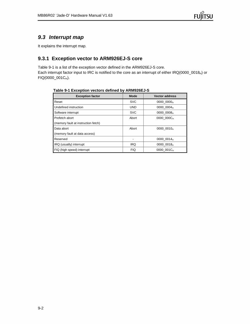
9-2
MB86R02 ‘Jade-D’ Hardware Manual V1.63
9.3 Interrupt map
It explains the interrupt map.
9.3.1 Exception vector to ARM926EJ-S core
Table 9-1 is a list of the exception vector defined in the ARM926EJ-S core. Each interrupt factor input to IRC is notified to the core as an interrupt of either IRQ(0000_0018H) or FIQ(0000_001CH).
Table 9-1 Exception vectors defined by ARM926EJ-S
Exception factor Mode Vector address
Reset SVC 0000_0000H
Undefined instruction UND 0000_0004H
Software interrupt SVC 0000_0008H
Prefetch abort
(memory fault at instruction fetch)
Abort 0000_000CH
Data abort
(memory fault at data access)
Abort 0000_0010H
Reserved - 0000_0014H
IRQ (usually) interrupt IRQ 0000_0018H
FIQ (high speed) interrupt FIQ 0000_001CH
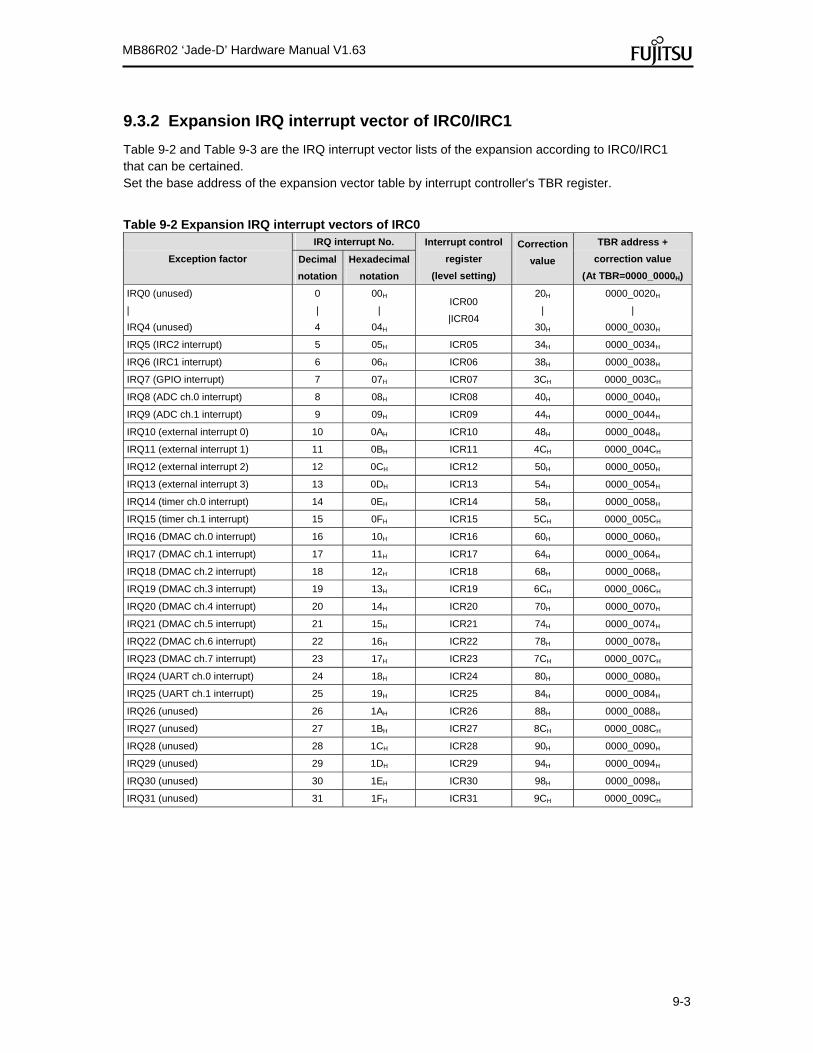
9-3
MB86R02 ‘Jade-D’ Hardware Manual V1.63
9.3.2 Expansion IRQ interrupt vector of IRC0/IRC1
Table 9-2 and Table 9-3 are the IRQ interrupt vector lists of the expansion according to IRC0/IRC1 that can be certained. Set the base address of the expansion vector table by interrupt controller's TBR register.
Table 9-2 Expansion IRQ interrupt vectors of IRC0
Exception factor
IRQ interrupt No. Interrupt control
register
(level setting)
Correction
value
TBR address +
correction value
(At TBR=0000_0000H)
Decimal
notation
Hexadecimal
notation
IRQ0 (unused)
|
IRQ4 (unused)
0
|
4
00H
|
04H
ICR00
|ICR04
20H
|
30H
0000_0020H
|
0000_0030H
IRQ5 (IRC2 interrupt) 5 05H ICR05 34H 0000_0034H
IRQ6 (IRC1 interrupt) 6 06H ICR06 38H 0000_0038H
IRQ7 (GPIO interrupt) 7 07H ICR07 3CH 0000_003CH
IRQ8 (ADC ch.0 interrupt) 8 08H ICR08 40H 0000_0040H
IRQ9 (ADC ch.1 interrupt) 9 09H ICR09 44H 0000_0044H
IRQ10 (external interrupt 0) 10 0AH ICR10 48H 0000_0048H
IRQ11 (external interrupt 1) 11 0BH ICR11 4CH 0000_004CH
IRQ12 (external interrupt 2) 12 0CH ICR12 50H 0000_0050H
IRQ13 (external interrupt 3) 13 0DH ICR13 54H 0000_0054H
IRQ14 (timer ch.0 interrupt) 14 0EH ICR14 58H 0000_0058H
IRQ15 (timer ch.1 interrupt) 15 0FH ICR15 5CH 0000_005CH
IRQ16 (DMAC ch.0 interrupt) 16 10H ICR16 60H 0000_0060H
IRQ17 (DMAC ch.1 interrupt) 17 11H ICR17 64H 0000_0064H
IRQ18 (DMAC ch.2 interrupt) 18 12H ICR18 68H 0000_0068H
IRQ19 (DMAC ch.3 interrupt) 19 13H ICR19 6CH 0000_006CH
IRQ20 (DMAC ch.4 interrupt) 20 14H ICR20 70H 0000_0070H
IRQ21 (DMAC ch.5 interrupt) 21 15H ICR21 74H 0000_0074H
IRQ22 (DMAC ch.6 interrupt) 22 16H ICR22 78H 0000_0078H
IRQ23 (DMAC ch.7 interrupt) 23 17H ICR23 7CH 0000_007CH
IRQ24 (UART ch.0 interrupt) 24 18H ICR24 80H 0000_0080H
IRQ25 (UART ch.1 interrupt) 25 19H ICR25 84H 0000_0084H
IRQ26 (unused) 26 1AH ICR26 88H 0000_0088H
IRQ27 (unused) 27 1BH ICR27 8CH 0000_008CH
IRQ28 (unused) 28 1CH ICR28 90H 0000_0090H
IRQ29 (unused) 29 1DH ICR29 94H 0000_0094H
IRQ30 (unused) 30 1EH ICR30 98H 0000_0098H
IRQ31 (unused) 31 1FH ICR31 9CH 0000_009CH

9-4
MB86R02 ‘Jade-D’ Hardware Manual V1.63
Table 9-3 Expansion IRQ interrupt vector of IRC1
Exception factor
IRQ interrupt No. Interrupt control
register
(level setting)
Correction
value
TBR address +
correction value
(At TBR=0000_0100H)
Decimal
notation
Hexadecimal
notation
IRQ0 (GDC interrupt) 0 00H ICR00 20H 0000_0120H
IRQ1 (unused) 1 01H ICR01 24H 0000_0124H
IRQ2 (CAN ch.0 interrupt) 2 02H ICR02 28H 0000_0128H
IRQ3 (CAN ch.1 interrupt) 3 03H ICR03 2CH 0000_012CH
IRQ4 (SD I/F interrupt) 4 04H ICR04 30H 0000_0130H
IRQ5 (unused) 5 05H ICR05 34H 0000_0134H
IRQ6 (I2S ch.0 interrupt) 6 06H ICR06 38H 0000_0138H
IRQ7 (unused) 7 07H ICR07 3CH 0000_013CH
IRQ8 (unused) 8 08H ICR08 40H 0000_0140H
IRQ9 (SPI interrupt) 9 09H ICR09 44H 0000_0144H
IRQ10 (unused) 10 0AH ICR10 48 H 0000_0148H
IRQ11 (I2C ch.0 interrupt) 11 0BH ICR11 4CH 0000_014CH
IRQ12 (I2C ch.1 interrupt) 12 0CH ICR12 50H 0000_0150H
IRQ13 (PWM ch.0 interrupt) 13 0DH ICR13 54H 0000_0154H
IRQ14 (PWM ch.1 interrupt) 14 0EH ICR14 58H 0000_0158H
IRQ15 (UART ch.2 interrupt) 15 0FH ICR15 5CH 0000_015CH
IRQ16 (UART ch.3 interrupt) 16 10H ICR16 60H 0000_0160H
IRQ17 (UART ch.4 interrupt) 17 11H ICR17 64H 0000_0164H
IRQ18 (UART ch.5 interrupt) 18 12H ICR18 68H 0000_0168H
IRQ19 (unused) 19 13H ICR19 6CH 0000_016CH
IRQ20 (unused) 20 14H ICR20 70H 0000_0170H
IRQ21 (unused) 21 15H ICR21 74H 0000_0174H
IRQ22 (unused) 22 16H ICR22 78H 0000_0178H
IRQ23 (unused) 23 17H ICR23 7CH 0000_017CH
IRQ24 (unused) 24 18H ICR24 80H 0000_0180H
IRQ25 (unused) 25 19H ICR25 84H 0000_0184H
IRQ26 (unused) 26 1AH ICR26 88H 0000_0188H
IRQ27 (unused) 27 1BH ICR27 8CH 0000_018CH
IRQ28 (unused) 28 1CH ICR28 90H 0000_0190H
IRQ29 (MLB_CINT interrupt) 29 1DH ICR29 94H 0000_0194H
IRQ30 (MLB_SINT interrupt) 30 1EH ICR30 98H 0000_0198H
IRQ31 (MLB_DINT interrupt) 31 1FH ICR31 9CH 0000_019CH
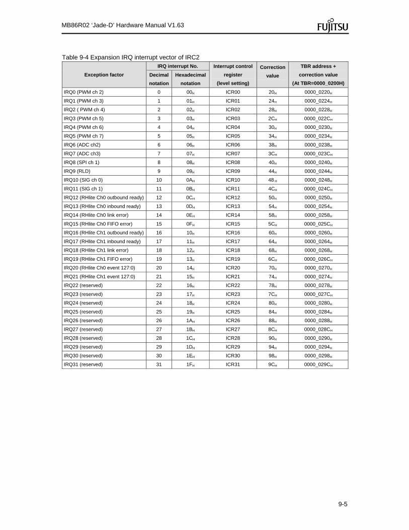
9-5
MB86R02 ‘Jade-D’ Hardware Manual V1.63
Table 9-4 Expansion IRQ interrupt vector of IRC2
Exception factor
IRQ interrupt No. Interrupt control
register
(level setting)
Correction
value
TBR address +
correction value
(At TBR=0000_0200H)
Decimal
notation
Hexadecimal
notation
IRQ0 (PWM ch 2) 0 00H ICR00 20H 0000_0220H
IRQ1 (PWM ch 3) 1 01H ICR01 24H 0000_0224H
IRQ2 ( PWM ch 4) 2 02H ICR02 28H 0000_0228H
IRQ3 (PWM ch 5) 3 03H ICR03 2CH 0000_022CH
IRQ4 (PWM ch 6) 4 04H ICR04 30H 0000_0230H
IRQ5 (PWM ch 7) 5 05H ICR05 34H 0000_0234H
IRQ6 (ADC ch2) 6 06H ICR06 38H 0000_0238H
IRQ7 (ADC ch3) 7 07H ICR07 3CH 0000_023CH
IRQ8 (SPI ch 1) 8 08H ICR08 40H 0000_0240H
IRQ9 (RLD) 9 09H ICR09 44H 0000_0244H
IRQ10 (SIG ch 0) 10 0AH ICR10 48 H 0000_0248H
IRQ11 (SIG ch 1) 11 0BH ICR11 4CH 0000_024CH
IRQ12 (RHlite Ch0 outbound ready) 12 0CH ICR12 50H 0000_0250H
IRQ13 (RHlite Ch0 inbound ready) 13 0DH ICR13 54H 0000_0254H
IRQ14 (RHlite Ch0 link error) 14 0EH ICR14 58H 0000_0258H
IRQ15 (RHlite Ch0 FIFO error) 15 0FH ICR15 5CH 0000_025CH
IRQ16 (RHlite Ch1 outbound ready) 16 10H ICR16 60H 0000_0260H
IRQ17 (RHlite Ch1 inbound ready) 17 11H ICR17 64H 0000_0264H
IRQ18 (RHlite Ch1 link error) 18 12H ICR18 68H 0000_0268H
IRQ19 (RHlite Ch1 FIFO error) 19 13H ICR19 6CH 0000_026CH
IRQ20 (RHlite Ch0 event 127:0) 20 14H ICR20 70H 0000_0270H
IRQ21 (RHlite Ch1 event 127:0) 21 15H ICR21 74H 0000_0274H
IRQ22 (reserved) 22 16H ICR22 78H 0000_0278H
IRQ23 (reserved) 23 17H ICR23 7CH 0000_027CH
IRQ24 (reserved) 24 18H ICR24 80H 0000_0280H
IRQ25 (reserved) 25 19H ICR25 84H 0000_0284H
IRQ26 (reserved) 26 1AH ICR26 88H 0000_0288H
IRQ27 (reserved) 27 1BH ICR27 8CH 0000_028CH
IRQ28 (reserved) 28 1CH ICR28 90H 0000_0290H
IRQ29 (reserved) 29 1DH ICR29 94H 0000_0294H
IRQ30 (reserved) 30 1EH ICR30 98H 0000_0298H
IRQ31 (reserved) 31 1FH ICR31 9CH 0000_029CH
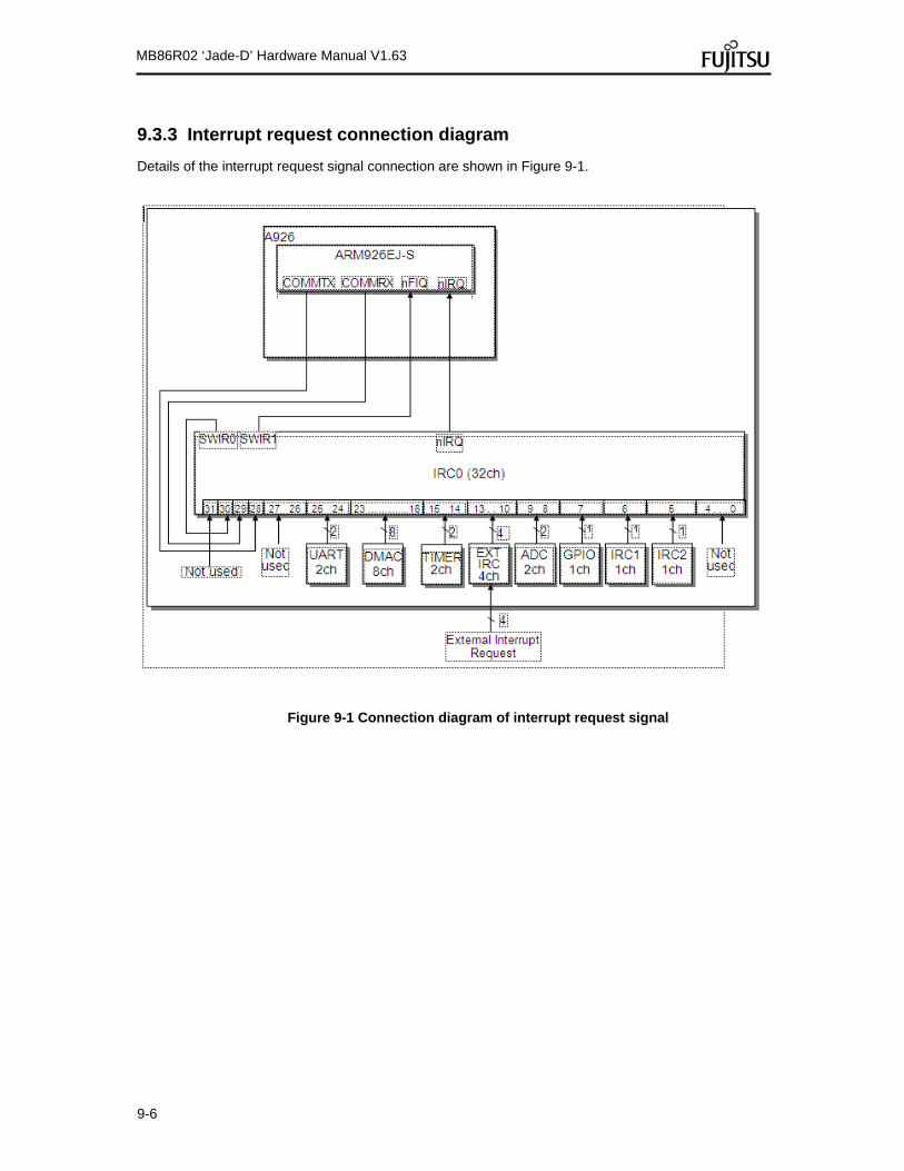
9-6
MB86R02 ‘Jade-D’ Hardware Manual V1.63
9.3.3 Interrupt request connection diagram
Details of the interrupt request signal connection are shown in Figure 9-1.
Figure 9-1 Connection diagram of interrupt request signal

9-7
MB86R02 ‘Jade-D’ Hardware Manual V1.63
9.4 Block diagram
The block diagram of IRC is shown in Figure 9-2.
ICR31
ICR00
ILM TBR
VCT
ICRMN
IRQ assertion
IRQF
IRQM
DICR1, 0
FIQ
Compare
Level determination IRQ vector generation
Display of accepted ICR level
IRQ assertion flag
Interrupt factor 00
FIQ
Cancellation ofSTOP/SLEEP mode
IRQTEST
IRQ interrupt control section
HRCL
CompareBus request cancel request
Bus request cancel request
Timing control
FIQTEST
Interrupt factor 29
Figure 9-2 Block diagram of IRC

9-8
MB86R02 ‘Jade-D’ Hardware Manual V1.63
9.5 Register
It explains the register of IRC.
9.5.1 Register list
The list of the register of IRC0 is shown in Table 9-5. The list of the register of IRC1 is shown in Table 9-6. The list of the register of IRC2 is shown in Table 9-7

9-9
MB86R02 ‘Jade-D’ Hardware Manual V1.63
Table 9-5 List of register of IRC0 Address
Register name Abbreviation Explanation Base Offset
FFFF_FE00H
or
FFFE_8000H
+ 00H IRQ flag register IRQF Control of IRQ interrupt flag
+ 04H IRQ mask register IRQM The mask of the assert of the IRQ interrupt is controlled.
+ 08H Interrupt level mask register ILM The interrupt level said to be valid from the ARM core is
set.
+ 0CH ICR monitoring register ICRMN The interrupt level of a current IRQ interrupt source is
displayed.
+ 10H Hold request cancellation
level register
HRCL The hold request cancellation level is set.
+ 14H Delay interrupt control
register
DICR The delay interrupt for the task switch is controlled.
+ 18H (Reserved) - It is a reserved area. (access prohibited)
+ 1CH Table base register TBR The upper address of the IRQ vector (24 bits) is set.
+ 20H Interrupt vector register VCT Display the interrupt vector table.
+ 24H IRQ test register IRQTEST The test of interrupt controller's IRQ interrupt function is
controlled. + 28H FIQ test register FIQTEST
+ 2CH (Reserved) - It is a reserved area. (access prohibited)
+ 30H Interrupt control register 0 ICR00 The level of the IRQ0 interrupt is set (unused and access
prohibited).
+ 34H Interrupt control register 1 ICR01 The level of the IRQ1 interrupt is set (unused and access
prohibited).
+ 38H Interrupt control register 2 ICR02 The level of the IRQ2 interrupt is set (unused and access
prohibited).
+ 3CH Interrupt control register 3 ICR03 The level of the IRQ3 interrupt is set (unused and access
prohibited).
+ 40H Interrupt control register 4 ICR04 The level of the IRQ4 interrupt is set (unused and access
prohibited).
+ 44H Interrupt control register 5 ICR05 The level of the IRQ5 interrupt is set (IRC2 interrupt).
+ 48H Interrupt control register 6 ICR06 The level of the IRQ6 interrupt is set (IRC1 interrupt).
+ 4CH Interrupt control register 7 ICR07 The level of the IRQ7 interrupt is set (GPIO interrupt).
+ 50H Interrupt control register 8 ICR08 The level of the IRQ8 interrupt is set (ADC ch.0 interrupt).
+ 54H Interrupt control register 9 ICR09 The level of the IRQ9 interrupt is set (ADC ch.1 interrupt).
+ 58H Interrupt control register 10 ICR10 The level of the IRQ10 interrupt is set (external interrupt
0).
+ 5CH Interrupt control register 11 ICR11 The level of the IRQ11 interrupt is set (external interrupt
1).
+ 60H Interrupt control register 12 ICR12 The level of the IRQ12 interrupt is set (external interrupt
2).
+ 64H Interrupt control register 13 ICR13 The level of the IRQ13 interrupt is set (external interrupt
3).
+ 68H Interrupt control register 14 ICR14 The level of the IRQ14 interrupt is set (timer ch.0
interrupt).
+ 6CH Interrupt control register 15 ICR15 The level of the IRQ15 interrupt is set (timer ch.1
interrupt).
+ 70H Interrupt control register 16 ICR16 The level of the IRQ16 interrupt is set (DMAC ch.0
interrupt).
+ 74H Interrupt control register 17 ICR17 The level of the IRQ17 interrupt is set (DMAC ch.1
interrupt).
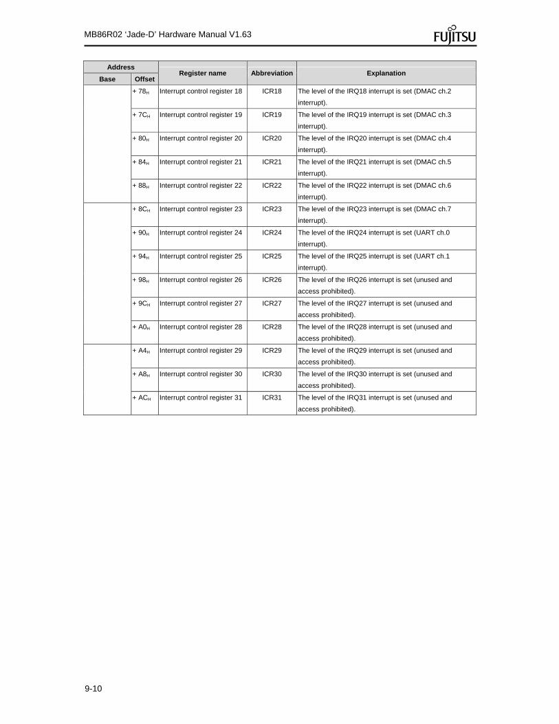
9-10
MB86R02 ‘Jade-D’ Hardware Manual V1.63
Address Register name Abbreviation Explanation
Base Offset
+ 78H Interrupt control register 18 ICR18 The level of the IRQ18 interrupt is set (DMAC ch.2
interrupt).
+ 7CH Interrupt control register 19 ICR19 The level of the IRQ19 interrupt is set (DMAC ch.3
interrupt).
+ 80H Interrupt control register 20 ICR20 The level of the IRQ20 interrupt is set (DMAC ch.4
interrupt).
+ 84H Interrupt control register 21 ICR21 The level of the IRQ21 interrupt is set (DMAC ch.5
interrupt).
+ 88H Interrupt control register 22 ICR22 The level of the IRQ22 interrupt is set (DMAC ch.6
interrupt).
+ 8CH Interrupt control register 23 ICR23 The level of the IRQ23 interrupt is set (DMAC ch.7
interrupt).
+ 90H Interrupt control register 24 ICR24 The level of the IRQ24 interrupt is set (UART ch.0
interrupt).
+ 94H Interrupt control register 25 ICR25 The level of the IRQ25 interrupt is set (UART ch.1
interrupt).
+ 98H Interrupt control register 26 ICR26 The level of the IRQ26 interrupt is set (unused and
access prohibited).
+ 9CH Interrupt control register 27 ICR27 The level of the IRQ27 interrupt is set (unused and
access prohibited).
+ A0H Interrupt control register 28 ICR28 The level of the IRQ28 interrupt is set (unused and
access prohibited).
+ A4H Interrupt control register 29 ICR29 The level of the IRQ29 interrupt is set (unused and
access prohibited).
+ A8H Interrupt control register 30 ICR30 The level of the IRQ30 interrupt is set (unused and
access prohibited).
+ ACH Interrupt control register 31 ICR31 The level of the IRQ31 interrupt is set (unused and
access prohibited).

9-11
MB86R02 ‘Jade-D’ Hardware Manual V1.63
Table 9-6 List of register of IRC1 Address
Register name Abbreviation Explanation Base Offset
FFFB_0000H
+ 00H IRQ flag register IRQF Control of IRQ interrupt flag
+ 04H IRQ mask register IRQM The mask of the assert of the IRQ interrupt is controlled.
+ 08H Interrupt level mask register ILM The interrupt level said to be valid from the ARM core is
set.
+ 0CH ICR monitoring register ICRMN The interrupt level of a current IRQ interrupt source is
displayed.
+ 10H Holding request cancellation
level register
HRCL The holding request cancellation level is set.
+ 14H Delay interrupt control
register
DICR The delay interrupt for the task switch is controlled.
+ 18H (Reserved) - It is a reserved area. (access prohibited)
+ 1CH Table base register TBR The upper address of the IRQ vector (24 bits) is set.
+ 20H Interrupt vector register VCT Display the interrupt vector table.
+ 24H IRQ test register IRQTEST The test of interrupt controller's IRQ interrupt function is
controlled. + 28H FIQ test register FIQTEST
+ 2CH (Reserved) - It is a reserved area. (access prohibited)
+ 30H Interrupt control register 0 ICR00 The level of the IRQ0 interrupt is set (GDC interrupt).
+ 34H Interrupt control register 1 ICR01 The level of the IRQ1 interrupt is set (unused and access
prohibited).
+ 38H Interrupt control register 2 ICR02 The level of the IRQ2 interrupt is set (CAN ch.0 interrupt).
+ 3CH Interrupt control register 3 ICR03 The level of the IRQ3 interrupt is set (CAN ch.1 interrupt).
+ 40H Interrupt control register 4 ICR04 The level of the IRQ4 interrupt is set (SD I/F interrupt).
+ 44H Interrupt control register 5 ICR05 The level of the IRQ5 interrupt is set (unused and access
prohibited).
+ 48H Interrupt control register ICR06 The level of the IRQ6 interrupt is set (I2S ch.0 interrupt).
+ 4CH Interrupt control register 7 ICR07 Unused
+ 50H Interrupt control register 8 ICR08 Unused
+ 54H Interrupt control register 9 ICR09 The level of the IRQ9 interrupt is set (SPI interrupt).
+ 58H Interrupt control register 10 ICR10 RESERVED
+ 5CH Interrupt control register 11 ICR11 The level of the IRQ11 interrupt is set (I2C ch.0 interrupt).
+ 60H Interrupt control register 12 ICR12 The level of the IRQ12 interrupt is set (I2C ch.1 interrupt).
+ 64H Interrupt control register 13 ICR13 The level of the IRQ13 interrupt is set (PWM ch.0
interrupt).
+ 68H Interrupt control register 14 ICR14 The level of the IRQ14 interrupt is set (PWM ch.1
interrupt).
+ 6CH Interrupt control register 15 ICR15 The level of the IRQ15 interrupt is set (UART ch.2
interrupt).
+ 70H Interrupt control register 16 ICR16 The level of the IRQ16 interrupt is set (UART ch.3
interrupt).
+ 74H Interrupt control register 17 ICR17 The level of the IRQ17 interrupt is set (UART ch.4
interrupt).
+ 78H Interrupt control register 18 ICR18 The level of the IRQ18 interrupt is set (UART ch.5
interrupt).
+ 7CH Interrupt control register 19 ICR19 Unused
+ 80H Interrupt control register 20 ICR20 Unused
+ 84H Interrupt control register 21 ICR21 Unused
+ 88H Interrupt control register 22 ICR22 Unused

9-12
MB86R02 ‘Jade-D’ Hardware Manual V1.63
Address Register name Abbreviation Explanation
Base Offset
+ 8CH Interrupt control register 23 ICR23 Unused
+ 90H Interrupt control register 24 ICR24 The level of the IRQ24 interrupt is set (unused and
access prohibited).
+ 94H Interrupt control register 25 ICR25 The level of the IRQ25 interrupt is set (unused and
access prohibited).
+ 98H Interrupt control register 26 ICR26 The level of the IRQ26 interrupt is set (unused and
access prohibited).
+ 9CH Interrupt control register 27 ICR27 The level of the IRQ27 interrupt is set (unused and
access prohibited).
+ A0H Interrupt control register 28 ICR28 The level of the IRQ28 interrupt is set (unused and
access prohibited).
+ A4H Interrupt control register 29 ICR29 The level of the IRQ29 interrupt is set (MLB_CINT
interrupt).
+ A8H Interrupt control register 30 ICR30 The level of the IRQ30 interrupt is set (MLB_SINT
interrupt).
+ ACH Interrupt control register 31 ICR31 The level of the IRQ31 interrupt is set (MLB_DINT
interrupt).
Table 9-7 List of register of IRC2 Address
Register name Abbreviation Explanation Base Offset
FFFB_1000H
+ 00H IRQ flag register IRQF Control of IRQ interrupt flag
+ 04H IRQ mask register IRQM The mask of the assert of the IRQ interrupt is controlled.
+ 08H Interrupt level mask register ILM The interrupt level said to be valid from the ARM core is
set.
+ 0CH ICR monitoring register ICRMN The interrupt level of a current IRQ interrupt source is
displayed.
+ 10H Holding request cancellation
level register
HRCL The holding request cancellation level is set.
+ 14H Delay interrupt control
register
DICR The delay interrupt for the task switch is controlled.
+ 18H (Reserved) - It is a reserved area. (access prohibited)
+ 1CH Table base register TBR The upper address of the IRQ vector (24 bits) is set.
+ 20H Interrupt vector register VCT Display the interrupt vector table.
+ 24H IRQ test register IRQTEST The test of interrupt controller's IRQ interrupt function is
controlled. + 28H FIQ test register FIQTEST
+ 2CH (Reserved) - It is a reserved area. (access prohibited)
+ 30H Interrupt control register 0 ICR00 The level of the IRQ0 (PWM ch 2)
+ 34H Interrupt control register 1 ICR01 The level of the IRQ1 (PWM ch 3)
+ 38H Interrupt control register 2 ICR02 The level of the IRQ2 ( PWM ch 4)
+ 3CH Interrupt control register 3 ICR03 The level of the IRQ3 (PWM ch 5)
+ 40H Interrupt control register 4 ICR04 The level of the IRQ4 (PWM ch 6)
+ 44H Interrupt control register 5 ICR05 The level of the IRQ5 (PWM ch 7)
+ 48H Interrupt control register 6 ICR06 The level of the IRQ6 (ADC ch 2)
+ 4CH Interrupt control register 7 ICR07 The level of the IRQ7 (ADC ch3)
+ 50H Interrupt control register 8 ICR08 The level of the IRQ8 (SPI ch 1)
+ 54H Interrupt control register 9 ICR09 The level of the IRQ9 (RLD)
+ 58H Interrupt control register 10 ICR10 The level of the IRQ10 (SIG ch 0)

9-13
MB86R02 ‘Jade-D’ Hardware Manual V1.63
Address Register name Abbreviation Explanation
Base Offset
+ 5CH Interrupt control register 11 ICR11 The level of the IRQ11 (SIG ch 1)
+ 60H Interrupt control register 12 ICR12 The level of the IRQ12 (RHlite Ch0 outbound ready)
+ 64H Interrupt control register 13 ICR13 The level of the IRQ13 (RHlite Ch0 inbound ready)
+ 68H Interrupt control register 14 ICR14 The level of the IRQ14 (RHlite Ch0 link error)
+ 6CH Interrupt control register 15 ICR15 The level of the IRQ15 (RHlite Ch0 FIFO error)
+ 70H Interrupt control register 16 ICR16 The level of the IRQ16 (RHlite Ch1 outbound ready)
+ 74H Interrupt control register 17 ICR17 The level of the IRQ17 (RHlite Ch1 inbound ready)
+ 78H Interrupt control register 18 ICR18 The level of the IRQ18 (RHlite Ch1 link error)
+ 7CH Interrupt control register 19 ICR19 The level of the IRQ19 (RHlite Ch1 FIFO error)
+ 80H Interrupt control register 20 ICR20 The level of the IRQ20 (RHlite Ch0 event 127:0)
+ 84H Interrupt control register 21 ICR21 The level of the IRQ21 (RHlite Ch1 event 127:0)
+ 88H Interrupt control register 22 ICR22 RESERVED
+ 8CH Interrupt control register 23 ICR23 RESERVED
+ 90H Interrupt control register 24 ICR24 RESERVED
+ 94H Interrupt control register 25 ICR25 RESERVED
+ 98H Interrupt control register 26 ICR26 RESERVED
+ 9CH Interrupt control register 27 ICR27 RESERVED
+ A0H Interrupt control register 28 ICR28 RESERVED
+ A4H Interrupt control register 29 ICR29 RESERVED
+ A8H Interrupt control register 30 ICR30 RESERVED
+ ACH Interrupt control register 31 ICR31 RESERVED
1) Ch0 TX ready: Successfull handover of data at the outbound interface = OutFIFO empty
(transition to empty) 2) Ch0 RX ready: Valid Data is received at inbound interface. Data is ready for read 3) Ch1 TX ready: Successfull handover of data at the outbound interface= OutFIFO empty
(transition to empty) 4) Ch1 RX ready: Valid Data is received at inbound interface. Data is ready for read 5) Ch0 Link Error: Ashell reports fatal condition 6) Ch1 Link Error: Ashell reports fatal condition 7) Ch0 Error: Reception FIFO over/underflow, Outbound error (write during busy) 8) Ch1 Error: Reception FIFO over/underflow, Outbound error (write during busy=OutFIFO
overflow)

9-14
MB86R02 ‘Jade-D’ Hardware Manual V1.63
Format of Register Descriptions The register descriptions in the following sections use the format shown below to describe each bit field of a register.
Address Base address + Offset
Bit 31 30 29 28 27 26 25 24 23 22 21 20 19 18 17 16
Name
R/W
Initial value
Bit 15 14 13 12 11 10 9 8 7 6 5 4 3 2 1 0
Name
R/W
Initial value
Meaning of items and sign Address
Address shows the address (Base address + Offset address) of the register. Bit
Bit shows bit number of the register. Name
Name shows bit field name of the register. R/W
R/W shows the read/write attribute of each bit field: R0: The read value is always "0". R1: The read value is always "1". W0: The write value is always "0". If "1" is written, it is ignored. W1: The write value is always "1". If "0" is written, it is ignored. R: Read W: Write
Initial value Initial value indicates the value of each bit field immediately after reset. 0: Initial value is "0". 1: Initial value is "1". X: Undefined.

9-15
MB86R02 ‘Jade-D’ Hardware Manual V1.63
9.5.2 IRQ flag register (IRQF)
The IRQF register controls the IRQ interrupt flag. The IRQF bit is set as a result of the IRQ interrupt source level decision when the interrupt levels are higher than the levels set in the ILM register, and the IRQ interrupt is asserted to the ARM core. When "0" is writed to the IRQF register, the IRQ interrupt to the ARM core is negated. When the IRQF bit is set, the interrupt vector is displayed in the VCT register. The address value of the VCT register is not changed until the IRQF bit is set.
Address IRC0:
FFFF_FE00H or FFFE_8000H + 00H
IRC1:FFFB_0000H + 00H
IRC2:FFFB_1000H + 00H
Bit 31 30 29 28 27 26 25 24 23 22 21 20 19 18 17 16
Name - - - - - - - - - - - - - - - -
R/W R/W R/W R/W R/W R/W R/W R/W R/W R/W R/W R/W R/W R/W R/W R/W R/W
Initial value X X X X X X X X X X X X X X X X
Bit 15 14 13 12 11 10 9 8 7 6 5 4 3 2 1 0
Name - - - - - - - - - - - - - - - IRQF
R/W R/W R/W R/W R/W R/W R/W R/W R/W R/W R/W R/W R/W R/W R/W R/W R/W
Initial value X X X X X X X X X X X X X X X 0
Bit field
Explanation Number Name
31-1 - It is an unused bit.
The write access is ignored. The read value of these bits is undefined.
0 IRQF It is IRQ interrupt flag.
The IRQF bit is set in "1" as a result of the IRQ interrupt level decision when it is higher than the
level to which the interrupt level is set in the ILM register (Interrupt level of ICR register >
Interrupt level of ILM register), and IRQX (interrupt request) is asserted to the ARM core.
0 IRQ is not asserted.
1 IRQ is asserted.
This bit is cleared by writing "0". It is invalid to write "1".

9-16
MB86R02 ‘Jade-D’ Hardware Manual V1.63
9.5.3 IRQ mask register (IRQM)
The IRQM register controls the mask of the assert of the IRQ interrupt.
Address IRC0:
FFFF_FE00H or FFFE_8000H + 04H
IRC1: FFFB_0000H + 04H
IRC2: FFFB_1000H + 04H
Bit 31 30 29 28 27 26 25 24 23 22 21 20 19 18 17 16
Name - - - - - - - - - - - - - - - -
R/W R/W R/W R/W R/W R/W R/W R/W R/W R/W R/W R/W R/W R/W R/W R/W R/W
Initial value X X X X X X X X X X X X X X X X
Bit 15 14 13 12 11 10 9 8 7 6 5 4 3 2 1 0
Name - - - - - - - - - - - - - - - IRQM
R/W R/W R/W R/W R/W R/W R/W R/W R/W R/W R/W R/W R/W R/W R/W R/W R/W
Initial value X X X X X X X X X X X X X X X 0
Bit field
Explanation Number Name
31-1 - It is an unused bit.
The write access is ignored. The read value of these bits is undefined.
0 IRQM The mask does the assert of the IRQ interrupt.
0 The assert of IRQ can certain the mask.
1 The assert of IRQ is valid.
This bit is initialized by reset by "0".
9.5.4 Interrupt level mask register (ILM)
The ILM register sets the interrupt level said to be valid from the ARM core. The interrupt controller notifies the ARM core the IRQ interrupt when the IRQ interrupt source is larger than the set value of this register. " Interrupt level of ICR register > Interrupt level of ILM register" -> Generated IRQ interrupt
Address IRC0:
FFFF_FE00H or FFFE_8000H + 08H
IRC1: FFFB_0000H + 08H
IRC2: FFFB_1000H + 08H
Bit 31 30 29 28 27 26 25 24 23 22 21 20 19 18 17 16
Name - - - - - - - - - - - - - - - -
R/W R/W R/W R/W R/W R/W R/W R/W R/W R/W R/W R/W R/W R/W R/W R/W R/W
Initial value X X X X X X X X X X X X X X X X
Bit 15 14 13 12 11 10 9 8 7 6 5 4 3 2 1 0
Name - - - - - - - - - - - - ILM3 ILM2 ILM1 ILM0
R/W R/W R/W R/W R/W R/W R/W R/W R/W R/W R/W R/W R/W R/W R/W R/W R/W
Initial value X X X X X X X X X X X X 1 1 1 1
Bit field
Explanation Number Name

9-17
MB86R02 ‘Jade-D’ Hardware Manual V1.63
Bit field Explanation
Number Name
31-4 - It is an unused bit.
The write access is ignored. The read value of these bits is undefined.
3-0 ILM3-0 These bits are used to set the IRQ interrupt level. Level value range is from 0000B or less to
1111B or more. (The IRQ interrupt doesn't occur. )
These bits are initialized by reset by 1111B.

9-18
MB86R02 ‘Jade-D’ Hardware Manual V1.63
9.5.5 ICR monitoring register (ICRMN)
The ICRMN register displays the interrupt level of a current IRQ interrupt source. 1111B is displayed if the IRQ interrupt source is not larger than the set value of this register. Moreover, the interrupt source at the highest level is displayed if the IRQ interrupt transmission source is larger than the set value of this register. When the IRQF bit of the IRQF register is set to "1", the ICRMN register is updated. The displayed interrupt level is not changed until the IRQF bit is cleared. Moreover, the interrupt level is decided again after the IRQF bit is cleared, and the display is updated by the source that sets the IRQF bit. When the IRQF bit is not made "1", the register value is not defined.
Address IRC0:
FFFF_FE00H or FFFE_8000H + 0CH
IRC1: FFFB_0000H + 0CH
IRC2: FFFB_1000H + 0CH
Bit 31 30 29 28 27 26 25 24 23 22 21 20 19 18 17 16
Name - - - - - - - - - - - - - - - -
R/W R/W R/W R/W R/W R/W R/W R/W R/W R/W R/W R/W R/W R/W R/W R/W R/W
Initial value X X X X X X X X X X X X X X X X
Bit 15 14 13 12 11 10 9 8 7 6 5 4 3 2 1 0
Name - - - - - - - - - - - - ICRMN3 ICRMN2 ICRMN1 ICRMN0
R/W R/W R/W R/W R/W R/W R/W R/W R/W R/W R/W R/W R/W R/W R/W R/W R/W
Initial value X X X X X X X X X X X X X X X X
Bit field
Explanation Number Name
31-4 - It is an unused bit.
The write access is ignored. The read value of these bits is undefined.
3-0 ILM3-0 The interrupt source at the highest level is displayed when the IRQ interrupt source is larger
than the set value of the ILM register.
The initial value of these bits is undefined.

9-19
MB86R02 ‘Jade-D’ Hardware Manual V1.63
9.5.6 Holding request cancellation level register (HRCL)
The HRCL register sets the holding request cancellation level. When the IRQ interrupt source is higher than the interrupt level set in the HRCL register, the holding request cancellation demand is asserted to the bus master.
Address IRC0:
FFFF_FE00H or FFFE_8000H + 10H
IRC1: FFFB_0000H + 10H
IRC2: FFFB_1000H + 10H
Bit 31 30 29 28 27 26 25 24 23 22 21 20 19 18 17 16
Name - - - - - - - - - - - - - - - -
R/W R/W R/W R/W R/W R/W R/W R/W R/W R/W R/W R/W R/W R/W R/W R/W R/W
Initial value X X X X X X X X X X X X X X X X
Bit 15 14 13 12 11 10 9 8 7 6 5 4 3 2 1 0
Name - - - - - - - - - - - - HRCL3 HRCL2 HRCL1 HRCL0
R/W R/W R/W R/W R/W R/W R/W R/W R/W R/W R/W R/W R/W R/W R/W R/W R/W
Initial value X X X X X X X X X X X X 1 1 1 1
Bit field
Explanation Number Name
31-4 - It is an unused bit.
The write access is ignored. The read value of these bits is undefined.
3-0 HRCL3-0 Set the holding request cancellation level.
These bits are used to set the IRQ interrupt level to issue the holding request cancellation
demand to bus masters other than ARM and TIC.
The bus request cancellation demand is issued when there is a high interrupt from the IRQ
interrupt at the highest level after IRQ interrupt priority is decided, and the interrupt level is set
to the HRCL register. This demand is asserted by the FIQ source.
Interrupt level of HRCL register < Interrupt level after the IRQ priority order of line interrupt is decided -> Issue of cancel request
FIQ interrupt source > Issue of cancel request
This function effects bus masters other than the ARM core and TIC directly. Besides, when
other bus masters when there is no bus master do not wait until this cancel request is input, it
becomes invalid.
This bit is initialized by reset by "1111B".

9-20
MB86R02 ‘Jade-D’ Hardware Manual V1.63
9.5.7 Delay interrupt control register (DICR)
The DICR register controls the delay interrupt for the task switch. The IRQ interrupt request can be issued, and software be cancelled by the writing operation to this register. The delay interrupt is allocated in IRQ30 of IRC0.
Address IRC0:
FFFF_FE00H or FFFE_8000H + 14H
IRC1: FFFB_0000H + 14H
IRC2: FFFB_1000H + 14H
Bit 31 30 29 28 27 26 25 24 23 22 21 20 19 18 17 16
Name - - - - - - - - - - - - - - - -
R/W R/W R/W R/W R/W R/W R/W R/W R/W R/W R/W R/W R/W R/W R/W R/W R/W
Initial value X X X X X X X X X X X X X X X X
Bit 15 14 13 12 11 10 9 8 7 6 5 4 3 2 1 0
Name - - - - - - - - - - - - - - - DLYI
R/W R/W R/W R/W R/W R/W R/W R/W R/W R/W R/W R/W R/W R/W R/W R/W R/W
Initial value X X X X X X X X X X X X X X X 0
Bit field
Explanation Number Name
31-1 - It is an unused bit.
The write access is ignored. The read value of these bits is undefined.
0 DLYI The delay interrupt is controlled.
Write "0" to this bit to cancel the delay interrupt.
0 The delay interrupt factor is cancelled. The interrupt request doesn't occur.
1 The delay interrupt factor is generated. The interrupt request occurs.
This bit is initialized by reset by "0".

9-21
MB86R02 ‘Jade-D’ Hardware Manual V1.63
9.5.8 Table base register (TBR)
The TBR register shows the upper address of the IRQ vector (24 bits). When the interrupt controller receives the IRQ interrupt source, and IRQ is asserted to the ARM core, the address displayed in the VCT register is as follows. (Set value of TBR register) + Individual IRQ interrupt source vector address
Address IRC0:
FFFF_FE00H or FFFE_8000H + 1CH
IRC1: FFFB_0000H + 1CH
IRC2: FFFB_1000H + 1CH
Bit 31 30 29 28 27 26 25 24 23 22 21 20 19 18 17 16
Name TBR31 TBR30 TBR29 TBR28 TBR27 TBR26 TBR25 TBR24 TBR23 TBR22 TBR21 TBR20 TBR19 TBR18 TBR17 TBR16
R/W R/W R/W R/W R/W R/W R/W R/W R/W R/W R/W R/W R/W R/W R/W R/W R/W
Initial value 0 0 0 0 0 0 0 0 0 0 0 0 0 0 0 0
Bit 15 14 13 12 11 10 9 8 7 6 5 4 3 2 1 0
Name TBR15 TBR14 TBR13 TBR12 TBR11 TBR10 TBR9 TBR8 Zero Zero Zero Zero Zero Zero Zero Zero
R/W R/W R/W R/W R/W R/W R/W R/W R/W R R R R R R R R
Initial value 0 0 0 0 0 0 0 0 0 0 0 0 0 0 0 0
Bit field
Explanation Number Name
31-8 TBR31-8 Set the upper address of the IRQ vector (24 bits).
These bits are initialized by reset by "0".
7-0 Zero These bits are the "0" fixation.
Writing is invalid. "0" can be read in the read value of these bits at any time.
These bits are initialized by reset by "0".
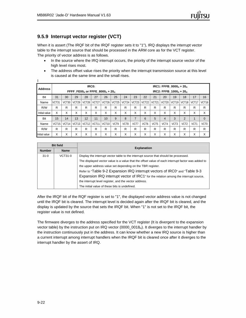
9-22
MB86R02 ‘Jade-D’ Hardware Manual V1.63
9.5.9 Interrupt vector register (VCT)
When it is assert (The IRQF bit of the IRQF register sets it to "1"), IRQ displays the interrupt vector table to the interrupt source that should be processed in the ARM core as for the VCT register. The priority of vector address is as follows.
In the source where the IRQ interrupt occurs, the priority of the interrupt source vector of the high level rises most.
The address offset value rises the priority when the interrupt transmission source at this level is caused at the same time and the small rises.
I
Address IRC0:
FFFF_FE00H or FFFE_8000H + 20H
IRC1: FFFB_0000H + 20H
IRC2: FFFB_1000H + 20H
Bit 31 30 29 28 27 26 25 24 23 22 21 20 19 18 17 16
Name VCT31 VCT30 VCT29 VCT28 VCT27 VCT26 VCT25 VCT24 VCT23 VCT22 VCT21 VCT20 VCT19 VCT18 VCT17 VCT16
R/W R R R R R R R R R R R R R R R R
Initial value X X X X X X X X X X X X X X X X
Bit 15 14 13 12 11 10 9 8 7 6 5 4 3 2 1 0
Name VCT15 VCT14 VCT13 VCT12 VCT11 VCT10 VCT9 VCT8 VCT7 VCT6 VCT5 VCT4 VCT3 VCT2 VCT1 VCT0
R/W R R R R R R R R R R R R R R R R
Initial value X X X X X X X X X X X X X X X X
Bit field
Explanation Number Name
31-0 VCT31-0 Display the interrupt vector table to the interrupt source that should be processed.
The displayed vector value is a value that the offset value of each interrupt factor was added to
the upper address value set depending on the TBR register.
Refer to "Table 9-2 Expansion IRQ interrupt vectors of IRC0" and "Table 9-3 Expansion IRQ interrupt vector of IRC1" for the relation among the interrupt source,
the interrupt level register, and the vector address.
The initial value of these bits is undefined.
After the IRQF bit of the RQF register is set to "1", the displayed vector address value is not changed until the IRQF bit is cleared. The interrupt level is decided again after the IRQF bit is cleared, and the display is updated by the source that sets the IRQF bit. When "1" is not set to the IRQF bit, the register value is not defined. The firmware diverges to the address specified for the VCT register (It is divergent to the expansion vector table) by the instruction put on IRQ vector (0000_0018H). It diverges to the interrupt handler by the instruction continuously put in the address. It can know whether a new IRQ source is higher than a current interrupt among interrupt handlers when the IRQF bit is cleared once after it diverges to the interrupt handler by the assert of IRQ.

9-23
MB86R02 ‘Jade-D’ Hardware Manual V1.63
9.5.10 IRQ test register (IRQTEST)
The IRQTEST register tests interrupt controller's IRQ interrupt function. When the ITEST bit of the FIQTEST register is "1", this register becomes valid. Set "0" to each bit of the IRQTEST register.
Address IRC0:
FFFF_FE00H or FFFE_8000H + 24H
IRC1: FFFB_0000H + 24H
IRC2: FFFB_1000H + 24H
Bit 31 30 29 28 27 26 25 24 23 22 21 20 19 18 17 16
Name ITST31 ITST30 ITST29 ITST28 ITST27 ITST26 ITST25 ITST24 ITST23 ITST22 ITST21 ITST20 ITST19 ITST18 ITST19 ITST36
R/W R/W R/W R/W R/W R/W R/W R/W R/W R/W R/W R/W R/W R/W R/W R/W R/W
Initial value 0 0 0 0 0 0 0 0 0 0 0 0 0 0 0 0
Bit 15 14 13 12 11 10 9 8 7 6 5 4 3 2 1 0
Name ITST15 ITST14 ITST13 ITST12 ITST11 ITST10 ITST9 ITST8 ITST7 ITST6 ITST5 ITST4 ITST3 ITST2 ITST1 ITST0
R/W R/W R/W R/W R/W R/W R/W R/W R/W R/W R/W R/W R/W R/W R/W R/W R/W
Initial value 0 0 0 0 0 0 0 0 0 0 0 0 0 0 0 0
Bit field
Explanation Number Name
31-4 ITST31-0 It is a control bit to test interrupt controller's IRQ interrupt function.
0 The interrupt is not generated.
1 The interrupt corresponding to IRQ is generated.
Set "0" to these bits.
Each bit is initialized by reset by "0".

9-24
MB86R02 ‘Jade-D’ Hardware Manual V1.63
9.5.11 FIQ test register (FIQTEST)
The FIQTEST register controls the test of interrupt controller's IRQ interrupt function.
Address IRC0:
FFFF_FE00H or FFFE_8000H + 28H
IRC1: FFFB_0000H + 28H
IRC2: FFFB_1000H + 28H
Bit 31 30 29 28 27 26 25 24 23 22 21 20 19 18 17 16
Name - - - - - - - - - - - - - - - -
R/W R/W R/W R/W R/W R/W R/W R/W R/W R/W R/W R/W R/W R/W R/W R/W R/W
Initial value X X X X X X X X X X X X X X X X
Bit 15 14 13 12 11 10 9 8 7 6 5 4 3 2 1 0
Name - - - - - - - - - - - - - - ITEST FTST
R/W R/W R/W R/W R/W R/W R/W R/W R/W R/W R/W R/W R/W R/W R/W R/W R/W
Initial value X X X X X X X X X X X X X X 0 0
Bit field
Explanation Number Name
31-2 - It is an unused bit.
The write access is ignored. The read value of these bits is undefined.
1 ITEST It is a control bit to test interrupt controller's IRQ interrupt function.
0 The interrupt is not generated with IRQTEST and the FIQTEST register.
1 The interrupt is generated with the ITST bit of the IRQTEST register and the FTST bit of
the FIQTEST register.
Set "0" to the ITEST bit.
This bit is initialized by reset by "0".
0 FTST It is a control bit to test interrupt controller's IRQ interrupt function.
When the ITEST bit is "1", the FTST bit becomes valid.
0 The interrupt is not generated.
1 The interrupt is generated.
Set "0" to the FTST bit.
This bit is initialized by reset by "0".

9-25
MB86R02 ‘Jade-D’ Hardware Manual V1.63
9.5.12 Interrupt control register (ICR31-ICR00)
The ICR31 to ICR00 register can be supplied to each IRQ interrupt source, and set the interrupt level of the corresponding IRQ interrupt source. The IRQ interrupt source can certain the mask when the ILM register is larger than the set value (Interrupt level of ICR register <= Interrupt level of ILM register).
Address
IRC0:
FFFF_FE00H or FFFE_8000H + 30H
|
FFFF_FE00H or FFFE_8000H + ACH
IRC1: FFFB_0000H + 30H --FFFB_0000H + ACH
IRC2: FFFB_1000H + 30H --FFFB_1000H + ACH
Bit 31 30 29 28 27 26 25 24 23 22 21 20 19 18 17 16
Name - - - - - - - - - - - - - - - -
R/W R/W R/W R/W R/W R/W R/W R/W R/W R/W R/W R/W R/W R/W R/W R/W R/W
Initial value X X X X X X X X X X X X X X X X
Bit 15 14 13 12 11 10 9 8 7 6 5 4 3 2 1 0
Name - - - - - - - - - - - - ICR3 ICR2 ICR1 ICR0
R/W R/W R/W R/W R/W R/W R/W R/W R/W R/W R/W R/W R/W R/W R/W R/W R/W
Initial value X X X X X X X X X X X X 1 1 1 1
Bit field
Explanation Num
ber
Name
31-4 - It is an unused bit.
The write access is ignored. The read value of these bits is undefined.

9-26
MB86R02 ‘Jade-D’ Hardware Manual V1.63
Bit field
Explanation Num
ber
Name
3-0 ICR3-0 These bits are used to set the interrupt level value of each interrupt source. Level value range
is lowest from height "0000B" "1111B".
ICR3 ICR3 ICR1 ICR0 Interrupt level
0 0 0 0 The highest level that can be set
0 0 0 1 (height)
0 0 1 0
0 0 1 1
0 1 0 0
0 1 0 1
0 1 1 0
0 1 1 1
1 0 0 0
1 0 0 1
1 0 1 0
1 0 1 1
1 1 0 0
1 1 0 1
1 1 1 0 (lowest)
1 1 1 1 Cannot the interrupt.
These bits are initialized by reset by "1111B".

9-27
MB86R02 ‘Jade-D’ Hardware Manual V1.63
9.6 Operation explanation
It explains the operation of IRC.
9.6.1 Outline of operation
It explains the outline of operation of the interrupt processing enumerating it as an example of the IRQ24 interrupt.
1. Refer to an instruction vector table address 0000_0080H for the ARM core when the IRQ interrupt is asserted to the ARM core as a result of the decision of priority of the IRQ24 interrupt source by the interrupt controller.
2. Loading instruction LDR PC,[PC,#_0×200] is writed to vector table address 0000_0018H beforehand. The expansion interrupt vector address of IRQ24 (value of the VCT register) refers to the vector address of IRQ24 in the expansion interrupt vector table by this instruction for it is possible to certain the load and the ARM core PC.
3. It is necessary to write the branch instruction to the IRQ24 interrupt handler to the expansion interrupt vector address of IRQ24. The interrupt handler of IRQ24 diverges by this branch instruction PC. It is necessary to dispose all interrupt handlers within ±32MB of the expansion interrupt vector table when the branch instruction is used. Use loading instruction LDR PC,[PC,#_xxx] instead of the branch instruction if the interrupt handler cannot dispose it within ±32MB.
LDR PC,[PC, #_0x200]
00000018H
IRQ24 interrupt handler
B IRQ24 Handler
00000018H
FFFFE20H
IRQ vector
Reference
VCT Register
Extended interrupt vector table00000018H
9.6.2 Initialization
Fix an individual exception table after the power-on. Set the expansion interrupt vector table. Store loading instruction LDR PC,[PC,#_0×200] to IRQ vector (00000018H) in the ARM core. Set the base address of the interrupt table to the TBR register. Set the interrupt level of each interrupt source to the ICR31-00 register. Set the interrupt level that the IRQ interrupt becomes valid for the ILM register. Set the flag of the CPSRs register in the ARM core to "0" (IRQ is valid). Do the interrupt valid according to the IRQM register among the interrupt controllers.

9-28
MB86R02 ‘Jade-D’ Hardware Manual V1.63
9.6.3 Multiple interrupt processing
The example of executing the multiple interrupt processing is shown.
M a in rou tin e
IR Q re que s t 1
T h e f irst in te rrup t p rocess (1 ) S av e th e registe r v a lu e in the s ta ck . (2 ) S av e a p re sen t IL M re gis te r v a lue and S P S R _irq
(e x isten ce in th e co re ) re g is te r v a lue in th e stack . D o no t lose b y th e fo llo w in g in te rrup t p ro cess. (3 ) S e t th e v a lue of th e IC R M N re giste r to the ILM regis te r,
a nd in te rrup t effe ctiv e ly a t a lev el tha t is h igh e r th an the f irst in te rru ption .
(4 ) T h e in te rrup tio n sou rce th a t is occu rring cu rren tly is c lea r.(5 ) T he IR Q F fla g is c le a r (N IR Q is neg a ted , an d th e de c is ion
o f th e in te rrup tio n lev el resta rts). (6 ) C on firm the cle a rn ess o f the IR Q flag . (7 ) C lea r I b it to the C P S R regis te r in the A R M 7 T D M I co re
a nd e nab le th e in te rrup tio n rece p tion .
IR Q req ue st 2
T he firs t in te rrup t re tu rn p rocessD o th e sam e in te rrup t re tu rn p roce ss a s th e seco nd to th e f irst in te rrup tio n.
T h e seco nd in te rrup tion p ro cessD o the sa m e in te rru p t p roce ss a s th e f irst to the se cond in te rrup tion .
T he se con d in te rru p tion re tu rn p roce ss (1 ) S e t I b it of the C P S R re g iste r, a nd
d isa b le the in te rru p tion . (2 ) R esto re the v a lu e of S P S R _ irq sav ed
in th e stack to th e S P S R _ irq reg iste r. (3 ) R esto re th e v alu e in th e stack to the
reg iste r. (4 ) R e sto re th e P C v alu e to re tu rn to form er
rou tin e , a nd resto re th e S P S R _irq reg iste r v a lue to the C P S R registe r.
C P S R S P S R _ irq
Figure 9-3 Multiple IRQ interrupt processing example
9.6.4 Example of IRQ interrupt handler
IRQ_Handler ROUT STMFD SP!, R0-R12, R14 ;The register value is preserved.
MESSAGE "Enter Dummy IRQ Handler"
LDR R0, = ILM
LDR R1, [R0]
MRS R2, SPSR
STMFD SP!, R1, R2 ;Preserve the value of ILM and the SPSR_irq register.
LDR R2, = ICRMN
LDR R1, [R2]
STR R1, [R0] ;Set the ICRMN register value to the ILM register.
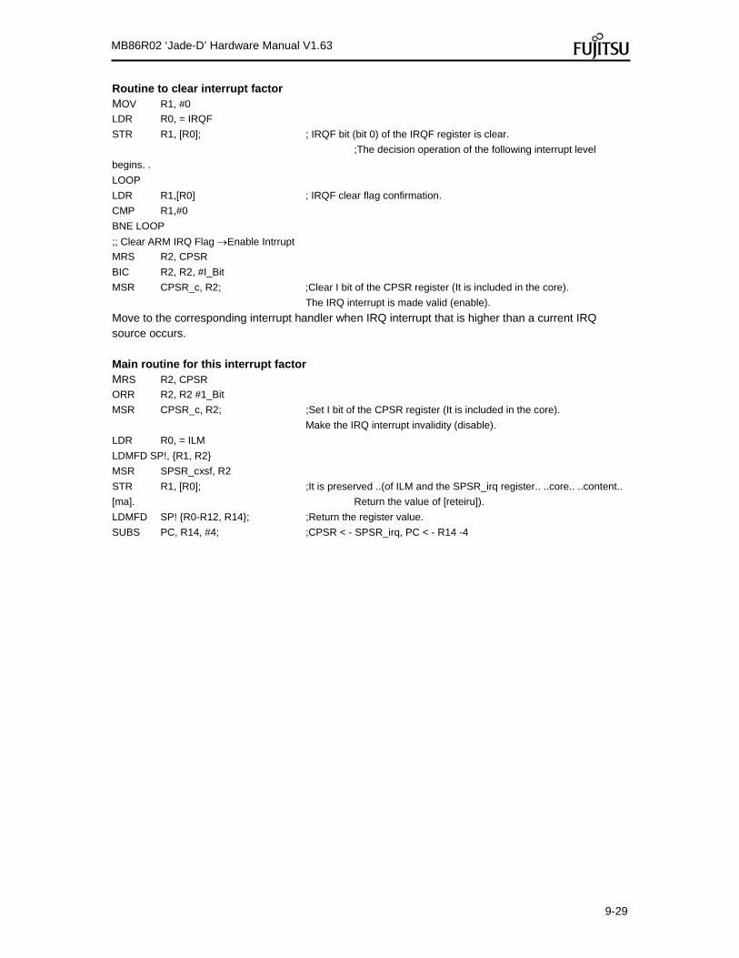
9-29
MB86R02 ‘Jade-D’ Hardware Manual V1.63
Routine to clear interrupt factor MOV R1, #0
LDR R0, = IRQF
STR R1, [R0]; ; IRQF bit (bit 0) of the IRQF register is clear.
;The decision operation of the following interrupt level
begins. .
LOOP
LDR R1,[R0] ; IRQF clear flag confirmation.
CMP R1,#0
BNE LOOP
;; Clear ARM IRQ Flag Enable Intrrupt
MRS R2, CPSR
BIC R2, R2, #I_Bit
MSR CPSR_c, R2; ;Clear I bit of the CPSR register (It is included in the core).
The IRQ interrupt is made valid (enable).
Move to the corresponding interrupt handler when IRQ interrupt that is higher than a current IRQ source occurs. Main routine for this interrupt factor MRS R2, CPSR
ORR R2, R2 #1_Bit
MSR CPSR_c, R2; ;Set I bit of the CPSR register (It is included in the core).
Make the IRQ interrupt invalidity (disable).
LDR R0, = ILM
LDMFD SP!, R1, R2
MSR SPSR_cxsf, R2
STR R1, [R0]; ;It is preserved ..(of ILM and the SPSR_irq register.. ..core.. ..content..
[ma]. Return the value of [reteiru]).
LDMFD SP! R0-R12, R14; ;Return the register value.
SUBS PC, R14, #4; ;CPSR < - SPSR_irq, PC < - R14 -4

9-30
MB86R02 ‘Jade-D’ Hardware Manual V1.63
9.6.5 Stop and return from sleep mode
The instruction of the return from the stop and sleep mode can be given to the clock controller by FIQ from the macro or issuing the IRQ interrupt.
The return signal from the stop and the sleep mode asserted to the ARM clock controller is generated with the OR of the FIQ factor asserted from IRQ factor and other macros that are higher than the interrupt level set depending on the ILM register (logical add). (Refer to Figure 9-1) It becomes impossible the return from the stop and sleep mode it therefore when the following interrupt factors occur. Note of return by FIQ source The factor occurs in the macro even if the FIQ factor is asserted and the return doesn't occur when masking alleged. This is because the interrupt is not transmitted by the interrupt controller. Note of return by IRQ factor The factor occurs in the macro even if the FIQ factor is asserted and the return doesn't occur when masking alleged. This is because the interrupt is not transmitted by the interrupt controller. The IRQ factor lowers more than the interrupt level set depending on the ILM register. When you do neither the stop by the FIQ factor nor the return from sleep mode
The interrupt of the mask by the macro. Set to become lower to the ILM register the level of the corresponding IRQ interrupt. Do not to transmit the interrupt to the interrupt controller for the DMA transfer in sleep mode,
and not to return from sleep mode.
9-31
MB86R02 ‘Jade-D’ Hardware Manual V1.63
9.6.6 Notes on use of IRC
The notes on use of IRC is described. Note concerning IRQ clear timing When "0" is writed to the IRQF bit of the IRQF register as described in the explanation of "9.5.2 IRQ flag register (IRQF)", IRQX to the ARM core (interrupt request) is negated. However, after "0" is writed to IRQF, IRQX is actually negated during one cycle of the APB clock. Therefore, when the code (interrupt handler) of which it is valid is the interrupt in the ARM core again immediately after "0" was writed to IRQF is written, the ARM core has the possibility of entering the IRQ mode again by mistake by IRQX before it is cleared. This has the possibility of occurring when the clock frequency in the ARM core is especially faster than the frequency of IRC. To evade this problem, add one dummy instruction (access instruction to the IRC interrupt register) after IRQF clear instruction. As a result, guarantee for IRQX to be cleared surely before the interrupt in the ARM core becomes valid again.

10-1
MB86R02 ‘Jade-D’ Hardware Manual V1.63
10 External Interrupt Controller (EXIRC) This chapter describes function and operation of external interrupt controller (EXIRC).
10.1 Outline
EXIRC is block to control external interrupt as well as external interrupt request input to external pin of INT_A[3] ~ INT_A [0]. "H" level, "L" level, rising edge, and falling edge are selectable as detected input request level.
10.2 Feature
EXIRC has following features: Operating as bus slave of AMBA (APB) 4 channels of external interrupt control 4 input request level selections
"H" level "L" level Rising edge Falling edge
Utilization of external interrupt as returning factor from Stop mode
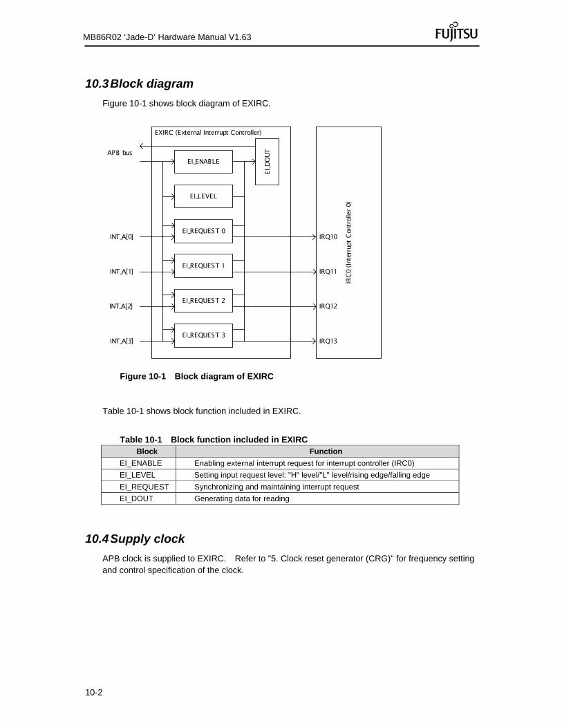
10-2
MB86R02 ‘Jade-D’ Hardware Manual V1.63
10.3 Block diagram
Figure 10-1 shows block diagram of EXIRC.
IRC0
(Int
erru
pt C
ontro
ller 0
)
EI_LEVEL
EI_ENABLE
EI_REQUEST 0
EI_REQUEST 1
EI_REQUEST 2
EI_REQUEST 3
EI_D
OUTAPB bus
INT_A[0] IRQ10
INT_A[1] IRQ11
INT_A[2] IRQ12
INT_A[3] IRQ13
EXIRC (External Interrupt Controller)
Figure 10-1 Block diagram of EXIRC Table 10-1 shows block function included in EXIRC.
Table 10-1 Block function included in EXIRC Block Function
EI_ENABLE Enabling external interrupt request for interrupt controller (IRC0)
EI_LEVEL Setting input request level: "H" level/"L" level/rising edge/falling edge
EI_REQUEST Synchronizing and maintaining interrupt request
EI_DOUT Generating data for reading
10.4 Supply clock
APB clock is supplied to EXIRC. Refer to "5. Clock reset generator (CRG)" for frequency setting and control specification of the clock.
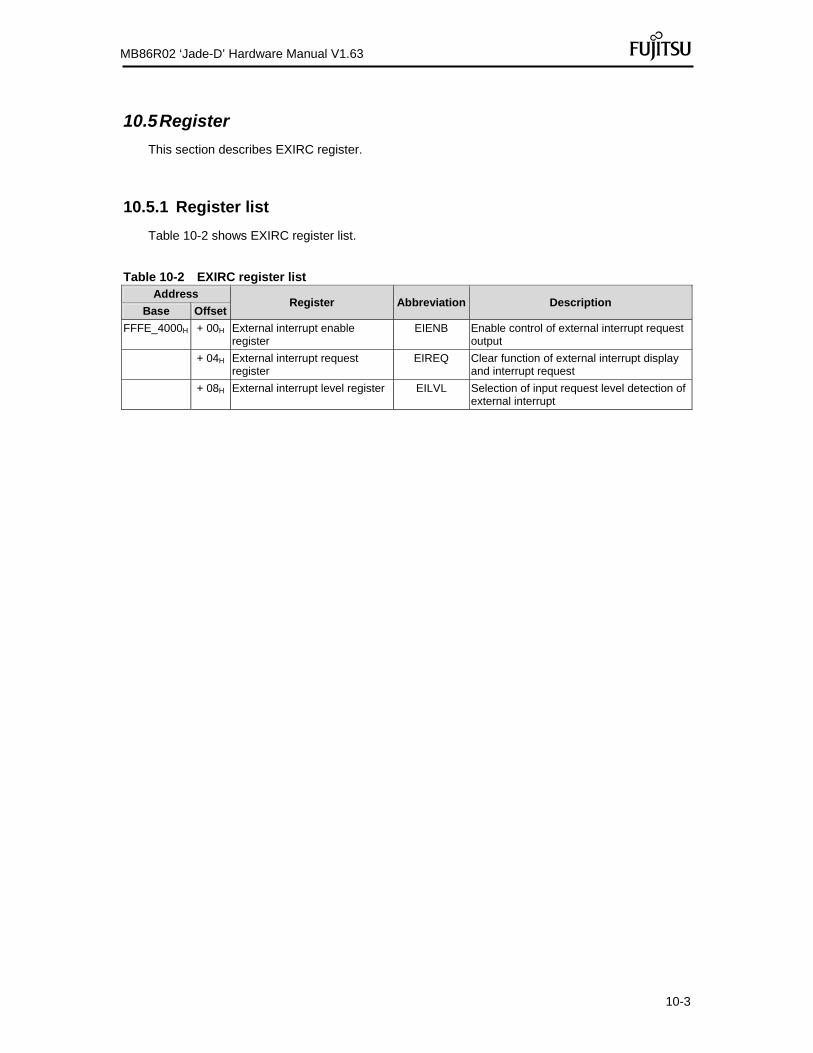
10-3
MB86R02 ‘Jade-D’ Hardware Manual V1.63
10.5 Register
This section describes EXIRC register.
10.5.1 Register list
Table 10-2 shows EXIRC register list.
Table 10-2 EXIRC register list Address
Register Abbreviation Description Base Offset
FFFE_4000H + 00H External interrupt enable register
EIENB Enable control of external interrupt request output
+ 04H External interrupt request register
EIREQ Clear function of external interrupt display and interrupt request
+ 08H External interrupt level register EILVL Selection of input request level detection of external interrupt

10-4
MB86R02 ‘Jade-D’ Hardware Manual V1.63
Description format of register Following format is used for description of register’s each bit in "10.5.2 External interrupt enable register (EIENB)" to "10.5.4 External interrupt level register (EILVL)".
Address Base address + Offset Bit 31 30 29 28 27 26 25 24 23 22 21 20 19 18 17 16
Name R/W
Initial value Bit 15 14 13 12 11 10 9 8 7 6 5 4 3 2 1 0
Name R/W
Initial value
Meaning of item and sign Address
Address (base address + offset address) of the register Bit
Bit number of the register Name
Bit field name of the register R/W
Attribution of read/write of each bit field R0:Read value is always "0" R1: Read value is always "1" W0: Write value is always "0", and write access of "1" is ignored W1: Write value is always "1", and write access of "0" is ignored R: Read W: Write Initial value
Each bit field’s value after reset 0: Value is "0" 1: Value is "1" X: Value is undefined

10-5
MB86R02 ‘Jade-D’ Hardware Manual V1.63
10.5.2 External interrupt enable register (EIENB)
This register is to control masking external interrupt request output.
Address FFFE_4000H + 00H Bit 31 30 29 28 27 26 25 24 23 22 21 20 19 18 17 16
Name – – – – – – – – – – – – – – – – R/W R/W R/W R/W R/W R/W R/W R/W R/W R/W R/W R/W R/W R/W R/W R/W R/W
Initial value X X X X X X X X X X X X X X X X Bit 15 14 13 12 11 10 9 8 7 6 5 4 3 2 1 0
Name – – – – – – – – – – – – ENB
3 ENB
2 ENB
1 ENB0
R/W R/W R/W R/W R/W R/W R/W R/W R/W R0 R0 R0 R0 R/W R/W R/W R/WInitial value X X X X X X X X 0 0 0 0 0 0 0 0
Bit field
Description No. Name
31-8 – Unused bit. Write access is ignored. Read value of these bits is undefined.
7-4 – Unused bit. Write access is ignored. Read value of these bits is always "0".
3-0 ENB3-0 Masking external interrupt request output is controlled.
0 External interrupt request is disabled
1 External interrupt request is enabled. The interrupt request output corresponding to the bit written "1" is permitted (ENB0 controls INT_A[0] permission), and the request is output to interrupt controller (IRC0.) Although the pin corresponding to the bit written "0" maintains interrupt factor, interrupt is not requested to the controller. These bits are initialized to "0000B" by reset.

10-6
MB86R02 ‘Jade-D’ Hardware Manual V1.63
10.5.3 External interrupt request register (EIREQ)
This register is to indicate and clear external interrupt request.
Address FFFE_4000H + 04H Bit 31 30 29 28 27 26 25 24 23 22 21 20 19 18 17 16
Name – – – – – – – – – – – – – – – – R/W R/W R/W R/W R/W R/W R/W R/W R/W R/W R/W R/W R/W R/W R/W R/W R/W
Initial value X X X X X X X X X X X X X X X X Bit 15 14 13 12 11 10 9 8 7 6 5 4 3 2 1 0
Name – – – – – – – – – – – – REQ
3 REQ
2 REQ
1 REQ
0 R/W R/W R/W R/W R/W R/W R/W R/W R/W R0 R0 R0 R0 R/W0 R/W0 R/W0 R/W0
Initial value X X X X X X X X 0 0 0 0 0 0 0 0
Bit field
Description No. Name
31-8 – Unused bit. Write access is ignored. Read value of these bits is undefined.
7-4 – Unused bit. Write access is ignored. Read value of these bits is always "0".
3-0 REQ3-0 External interrupt request is indicated and cleared.
0 At reading: There is no external interrupt request At writing: External interrupt request is cleared
1 At reading: There is external interrupt request At writing: External interrupt request invalid
Read value of "1" shows external interrupt is requested. These bits correspond to external interrupt channel as follows.
REQ0: External interrupt 0 (INT_A[0] pin) REQ1: External interrupt 1 (INT_A[1] pin) REQ2: External interrupt 2 (INT_A[2] pin) REQ3: External interrupt 3 (INT_A[3] pin)
When "0" is written to these bits, external interrupt request is cleared. Writing "1" is invalid. These bits are initialized to "0000B" by reset.

10-7
MB86R02 ‘Jade-D’ Hardware Manual V1.63
10.5.4 External interrupt level register (EILVL)
This register is to select input request level detection.
Address FFFE_4000H + 08H Bit 31 30 29 28 27 26 25 24 23 22 21 20 19 18 17 16
Name – – – – – – – – – – – – – – – – R/W R/W R/W R/W R/W R/W R/W R/W R/W R/W R/W R/W R/W R/W R/W R/W R/W
Initial value X X X X X X X X X X X X X X X X Bit 15 14 13 12 11 10 9 8 7 6 5 4 3 2 1 0
Name – – – – – – – – LVL3[1] LVL3[0] LVL2[1] LVL2[0] LVL1[1] LVL1[0] LVL0[1] LVL0[0]R/W R/W R/W R/W R/W R/W R/W R/W R/W R/W R/W R/W R/W R/W R/W R/W R/W
Initial value X X X X X X X X 0 1 0 1 0 1 0 1
Bit field
Description No. Name
31-8 – Unused bit. Write access is ignored. Read value of these bits is undefined.
7-0 LVL3[1:0] - LVL0[1:0] Input request level detection of external interrupt is selected. 2 bit is allocated to each external interrupt channel. This is initialized to "01B" by reset.
LVL0[1:0]: External interrupt 0 (INT_A[0] pin) LVL1[1:0]: External interrupt 1 (INT_A[1] pin) LVL2[1:0]: External interrupt 2 (INT_A[2] pin) LVL3[1:0]: External interrupt 3 (INT_A[3] pin)
LVL3-0[1] LVL3-0[0] Input request level
0 0 "L" Level
0 1 "H" Level
1 0 Rising edge
1 1 Falling edge

10-8
MB86R02 ‘Jade-D’ Hardware Manual V1.63
10.6 Operation
External interrupt controller issues request signal to interrupt controller (IRC0) when input request level of external interrupt is input to corresponding channel after setting EIENB and EILVL registers. If interrupt from this module is higher than interrupt level set in ILM register and it is highest priority as a result of interrupt prioritization occurred in IRQ level decision circuit, IRQ interrupt request is issued to ARM core.
IRC0 (Interrupt Controller 0)
IRQyy
Compare interrupt level
ILM
IRQ External Interrupt Controller
From external pins
Figure 10-2 Operation of external interrupt
10.7 Operation procedure
External interrupt register setting procedure is as followings. 1. Disable EIENB register related bit 2. Set EILVL register related bit 3. Clear EIREQ register related bit 4. Enable EIENB register related bit
EIENB register must be disabled to set register in the module; moreover, EIREQ register needs to be cleared before EIENB register is enabled. This operation is to prevent accident caused by incidental interrupt source during register setting.
10.8 Instruction for use
This section indicates notice for using external interrupt.
Notice for returning from Stop mode When external interrupt is used to return from Stop mode, where clock is stopped, set input request level to "H" since "L" level request may cause malfunction. Moreover, the edge request is not able to return from the Stop mode.

11-1
MB86R02 ‘Jade-D’ Hardware Manual V1.63
11 External Bus Interface This chapter describes external bus of MB86R02.
11.1 Outline
MB86R02 has external bus interface for accessing to external memory device such as SRAM and Flash.
11.2 Features
External bus interface of MB86R02 has the following features. Supporting 16/32 bit (32 bit is an option) width of SRAM/Flash 3 chip selections for SRAM/Flash (MEM_XCS[4] is for boot operation). Parameter setting by individual chip selection for SRAM/Flash Supporting NOR flash page access Supporting Bi-endian
11.3 Block diagram
Figure 11-1 shows block diagram of external bus interface.
CC
PB
AH
B B
us
External
Bus I/F
AHB I/F
Sw
itch
er
MEM_RDY
MEM_XCS[4/2/0]
MEM_XRD
MEM_EA[24:1]
(MEM_XWR[3:2])
MEM_XWR[1:0]
(MEM_ED[31:16])
MEM_ED[15:0]
MPX_MODE_1[1:0]
BIGEND MB86R01
Figure 11-1 Block diagram of external bus interface part

11-2
MB86R02 ‘Jade-D’ Hardware Manual V1.63
11.4 Related pin
Table 11-1 External interface pin Pin I/O No. of pin Function
MEM_EA[24:1] O 24 Address bus
MEM_XWR[3:0] O 4
Writing enabled Upper 2 bits are multiplexed pin
MEM_XRD O 1 Reading enabled
MEM_XCS[4] O 1 Chip selection for boot operation
MEM_XCS[2] O 1 Chip selection
MEM_XCS[0] O 1 Chip selection
MEM_ED[31:0] IO 32
Data bus Upper 16 bits are multiplexed pin
MEM_RDY I 1 Ready input for low-speed device
11.5 Supply clock
AHB clock is supplied to external bus interface. Refer to "5. Clock reset generator (CRG)" for frequency setting and control specification of the clock.

11-3
MB86R02 ‘Jade-D’ Hardware Manual V1.63
11.6 Register
This section describes 32 bit width external bus I/F register. Be sure to access to it in word (32 bit.)
11.6.1 SRAM/Flash mode register 0/2/4 (MCFMODE0/2/4)
Register address
BaseAddress+0x0000(MEM_XCS[0]), BaseAddress+0x0008(MEM_XCS [2]), BaseAddress+0x0010(MEM_XCS [4])
Bit No. 31 30 29 28 27 26 25 24 23 22 21 20 19 18 17 16 Bit field name Reserved
R/W R/W0 Initial value X
Bit No. 15 14 13 12 11 10 9 8 7 6 5 4 3 2 1 0
Bit field name Reserved RDYPAG
E Reserved WDTH
R/W R/W0 R/W R/W R/W0 R/W Initial value X 0 0 X X X 0 *1
Bit31-7: Reserved
Reserved bits. Write "0" to these bits. Their read value is undefined.
Bit6: RDY (ready mode) When handshake is performed with low-speed peripherals that use MEM_RDY signal, set this bit to "1". RDY signal at reading should be asserted to "L" at least 2 cycles from 2 cycles before falling edge of MEM_XRD signal to actual falling edge. For the writing operation, the RDY signal should also be asserted to "L" at least 2 cycles from 2 cycles before falling edge of MEM_XWR signal to actual falling edge. For accessing to device such as SRAM memory without using the MEM_RDY signal, this bit should be set to "0".
0: READY mode OFF (initial value) 1: READY mode ON
Bit5: PAGE (page access mode) NOR flash page access mode
This bit controls NOR flash page access mode which issues the first address cycle according to FirstReadAddressCycle (FRADC) setting. Then, the access is continuously executed according to Read Access Cycle (RACC) setting until it reaches to 16 byte boundary. In order to select this mode, set Read Address Cycle (RADC) to 0.
0: NOR flash page access mode OFF (initial value) 1: NOR flash page access mode ON
Bit4-2: Reserved
Reserved bits. Write "0" to these bits. Their read value is undefined.
Note: Writing "1" to these bits are prohibited.

11-4
MB86R02 ‘Jade-D’ Hardware Manual V1.63
Bit1-0: WDTH (data width) These bits specify data bit width of the connected device.
0: 8 bit (initial value) 1: 16 bit 2: 32 bit 3: Reserved
*1: Initial value of data width to MEM_XCS[4]
MPX_MODE_1[1:0] = 2’b01 or 2'b10: 2:32 bit Others: 1:16 bit
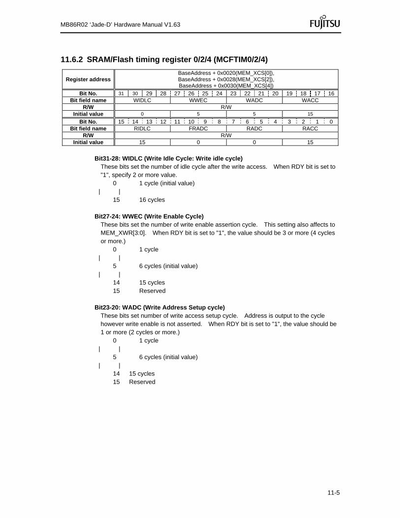
11-5
MB86R02 ‘Jade-D’ Hardware Manual V1.63
11.6.2 SRAM/Flash timing register 0/2/4 (MCFTIM0/2/4)
Register address BaseAddress + 0x0020(MEM_XCS[0]), BaseAddress + 0x0028(MEM_XCS[2]), BaseAddress + 0x0030(MEM_XCS[4])
Bit No. 31 30 29 28 27 26 25 24 23 22 21 20 19 18 17 16 Bit field name WIDLC WWEC WADC WACC
R/W R/W Initial value 0 5 5 15
Bit No. 15 14 13 12 11 10 9 8 7 6 5 4 3 2 1 0 Bit field name RIDLC FRADC RADC RACC
R/W R/W Initial value 15 0 0 15
Bit31-28: WIDLC (Write Idle Cycle: Write idle cycle)
These bits set the number of idle cycle after the write access. When RDY bit is set to "1", specify 2 or more value.
0 1 cycle (initial value) | |
15 16 cycles
Bit27-24: WWEC (Write Enable Cycle) These bits set the number of write enable assertion cycle. This setting also affects to MEM_XWR[3:0]. When RDY bit is set to "1", the value should be 3 or more (4 cycles or more.)
0 1 cycle | |
5 6 cycles (initial value) | |
14 15 cycles 15 Reserved
Bit23-20: WADC (Write Address Setup cycle)
These bits set number of write access setup cycle. Address is output to the cycle however write enable is not asserted. When RDY bit is set to "1", the value should be 1 or more (2 cycles or more.)
0 1 cycle | |
5 6 cycles (initial value) | |
14 15 cycles 15 Reserved
11-6
MB86R02 ‘Jade-D’ Hardware Manual V1.63
Bit19-16: WACC (Write Access Cycle) These bits specify number of cycle required for write access. The address does not change during the cycle specified in these bits. This value should be larger than the total number of Address Setup Cycle (WADC) and Write Enable Cycle (WWEC). When RDY bit is set to "1", the value should be 6 or more (7 cycles or more.)
0, 1 Reserved 2 3 cycles
| | 15 16 cycles (initial value)
Bit15-12: RIDLC (Read Idle Cycle)
These bits set number of idle cycle after read access. They are used to prevent data collision that occurs by write access immediately after the read access.
0 1 cycle
| | 15 16 cycles (initial value)
Bit11-8: FRADC (First Read Address Cycle)
These bits are exclusive use for NOR Flash setting that corresponds to page mode access, and are set initial latency in the address of Flash read access. The address is retained with number of cycle specified by these bits only at the first read access. The subsequent read access is executed according to the number of cycle set in the RACC. MEM_XCS[0/2/4] and MEM_XRD are asserted simultaneously. When other values than 0 are set to these bits, specify "0" to RADC (Read Address Setup Cycle.)
0 0 cycle (initial value) | |
15 15 cycles
Bit7-4: RADC (Read Address Setup cycle) These bits set number of read address setup cycle which asserts MEM_XCS[0/2/4] and its address but not MEM_XRD. When 0 is selected, MEM_XRD and MEM_XCS[0/2/4] are asserted simultaneously. The specifying value should be within number of the read access setup cycle. When NOR Flash page access mode is applied, set these bits to "0". When RDY bit is set to "1", the value should be 3 or more (3 cycles or more.)
0 0 cycle (initial value) | |
15 15 cycles
Bit3-0: RACC (Read Access Cycle) These bits set number of cycle required for the read access. Although the address does not change during the cycle specified by these bits, data is fetched at the last cycle. When RDY bit is set to "1", the value should be 3 or more (4 cycles or more.)
0 1 cycle | |

11-7
MB86R02 ‘Jade-D’ Hardware Manual V1.63
15 16 cycles (initial value)

11-8
MB86R02 ‘Jade-D’ Hardware Manual V1.63
11.6.3 SRAM/Flash area register 0/2/4 (MCFAREA0/2/4)
Register address BaseAddress + 0x0040(MEM_XCS[0]), BaseAddress + 0x0048(MEM_XCS[2]), BaseAddress + 0x0050(MEM_XCS[4])
Bit No. 31 30 29 28 27 26 25 24 23 22 21 20 19 18 17 16 Bit field name Reserved MASK
R/W R/W0 R/W Initial value X 15 (16MB width)
Bit No. 15 14 13 12 11 10 9 8 7 6 5 4 3 2 1 0 Bit field name Reserved ADDR
R/W R/W0 R/W Initial value X (in order of MEM_XCS[0/2/4]) 64,32,0
Bit31-23: Reserved
Reserved bits. Write "0" to these bits. Their read value is undefined.
Bit22-16: MASK (Address mask)
These bits set mask value of the one set to ADDR. This external bus interface masks ADDR (masked with setting "1") and internal bus mask address according to the specified mask to compare them. When they are matched, external bus interface accesses to MEM_XCS[4/2/0] signal. [22:16] masks each address [26:20].
(Example)
ADDR = 00001000 (b) MASK = 0000011 (b)
<When the device is selected> Internal bus address (external interface address): AD = 0x10900000 Mask ADDR & (!MASK) = 00001000 (b) AD [27:20] & (!MASK) = 00001000 (b) ….. Matched, and this device is selected
<When the device is not selected> Internal bus address (external interface address): AD = 0x10c00000 Masking ADDR & (!MASK) = 00001000 (b) AD [27:20] & (!MASK) = 00001100 (b) ….. Unmatched, and device is not selected The masking selects area size; in this example, 0x10800000 - 0x10b00000 (4MB) are selected. The bit specified "1" with masking is lost during mask processing. These bits are invalid even if they are set to ADDR. When LSB in the example is 1 (ADDR = 00001001 (b)), the same address field is selected since it is invalid in masking. The correlation of the size in mask setting and address field is shown below. 0000000 (b) 1MB 0001111 (b) 16MB 0000001 (b) 2MB 0011111 (b) 32MB

11-9
MB86R02 ‘Jade-D’ Hardware Manual V1.63
0000011 (b) 4MB 0111111 (b) 64MB 0000111 (b) 8MB 1111111 (b) 128MB
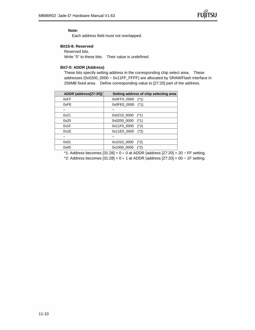
11-10
MB86R02 ‘Jade-D’ Hardware Manual V1.63
Note: Each address field must not overlapped.
Bit15-8: Reserved
Reserved bits. Write "0" to these bits. Their value is undefined.
Bit7-0: ADDR (Address)
These bits specify setting address in the corresponding chip select area. These addresses (0x0200_0000 ~ 0x11FF_FFFF) are allocated by SRAM/Flash interface in 256MB fixed area. Define corresponding value to [27:20] part of the address. ADDR (address[27:20]) Setting address of chip selecting area
0xFF 0x0FF0_0000 (*1)
0xFE 0x0FE0_0000 (*1)
~ ~
0x21 0x0210_0000 (*1)
0x20 0x0200_0000 (*1)
0x1F 0x11F0_0000 (*2)
0x1E 0x11E0_0000 (*2)
~ ~
0x01 0x1010_0000 (*2)
0x00 0x1000_0000 (*2)
*1: Address becomes [31:28] = 0 0 at ADDR (address [27:20] = 20 ~ FF setting. *2: Address becomes [31:28] = 0 1 at ADDR (address [27:20] = 00 ~ 1F setting.

11-11
MB86R02 ‘Jade-D’ Hardware Manual V1.63
11.6.4 Memory controller error register (MCERR)
Register address BaseAddress + 0x0200
Bit No. 31 30 29 28 27 26 25 24 23 22 21 20 19 18 17 16 Bit field name Reserved
R/W R/W0 Initial value X
Bit No. 15 14 13 12 11 10 9 8 7 6 5 4 3 2 1 0
Bit field name Reserved Reserved SFIO
N Reserved SFER
R/W R/W0 R/W0 R/W R R/W0
Initial value X 0 0 0 0
Bit31-4: Reserved
Reserved bits. Write "0" to these bits. Their value is undefined.
Bit3: Reserved
Reserved bit. Write "0" to these bits. Their value is undefined.
Note: Writing "1" to this bit is prohibited.
Bit2: SFION (SRAM/Flash error interrupt: ON)
This bit validates interrupt at SRAM/Flash error. 0: OFF (initial value) 1: ON
Bit1: Reserved
Reserved bit. Write 0 to these bits. Their value is undefined.
Bit0: SFER (SRAM/Flash error)
This bit indicates that the area without mapping is accessed. In this case, memory controller returns error to internal bus; at the same time, this bit, is set. When the value is "1", it is cleared by writing "0" Only when "1" is set to this bit, clear operation is available.
0: No error (Initial value) 1: Error

11-12
MB86R02 ‘Jade-D’ Hardware Manual V1.63
11.7 Connection example
16 bit NOR Flash
16 bit NOR Flash + 8 bit SRAM 2
MB86R02
MEM_EA[24:1] MEM_XCS[4]
MEM_XRD MEM_XWR[0]
MEM_ED[15:0]
x16 NOR Flash
A XCE XOE XWE DQ[15:0]
MB86R02
x8 SRAM
x8 SRAM
MEM_ED[7:0]
MEM_ED[15:8]
MEM_EA[24:1] MEM_XCS[0]
MEM_XRD MEM_XWR[1:0] MEM_ED[15:0]
MEM_XCS[4]
MEM_XWR[0]
MEM_XWR[1]
A CSn OEn WEn DQ[7:0]
A CSn OEn WEn DQ[7:0]
x16 NOR Flash
A XCE XOE XWE DQ[15:0]
MEM_XWR[0]
MEM_ED[15:0]

11-13
MB86R02 ‘Jade-D’ Hardware Manual V1.63
11.8 Example of access waveform
Word read access to 16 bit width SRAM/NOR Flash
Word write access to 16 bit width SRAM/NOR Flash

11-14
MB86R02 ‘Jade-D’ Hardware Manual V1.63
Read/Write to low-speed device
Figure 11-2 Half word read access to 16 bit width low speed device
XMEM_EA[24:1] 00
D00
X
MEM_ED[15:0]
MEM_XRD
MEM_XWR[1:0]
MEM_XCS[4/2/0]
Internal clock
MEM_RDY
tWACC + Wait cycle
tWADC = Write address setup cycle
tWADC
Min 2 cycles
tWACC = Write access cycle
tWIDLC
Wait cycle
tWWEC = Write enable cycle
tWWEC
X
tWIDLC = Write idle cycle
1 cycle1 cycle
Figure 11-3 Half word write access to 16 bit width low speed device

11-15
MB86R02 ‘Jade-D’ Hardware Manual V1.63
Figure 11-4 Word read access to 16bit low speed device
01 X
D01
MEM_EA[24:1] 00
D00
X
MEM_ED[15:0]
MEM_XRD
MEM_XWR[1:0]
MEM_XCS[4/2/0]
Internal clock
MEM_RDY
tWACC + Wait1 cycle + tWACC + Wait2 cycle
tWADC = write address setup cycle
tWADC
Min 2 cycles
tWACC = Write access cycle
tWADC
Min 2 cycles
tWIDLC
Wait1 cycle Wait2 cycle
tWWEC = Write enable cycle
tWWEC
X
tWWEC
tWIDLC = Write idle cycle
1 cycle1 cycle1 cycle
Figure 11-5 Word write access to 16bit low speed device

11-16
MB86R02 ‘Jade-D’ Hardware Manual V1.63
Page read of 16 bit NOR Flash
02MEM_EA[24:1] 00
D00
X
MEM_ED[15:0]
MEM_XRD
MEM_XWR[1:0]
MEM_XCS[4/2/0]
Internal clock
MEM_RDY
tFRADC = First read access cycle
tRACC = Read access cycle
tFRADC
X
04 06 08 0A
tRACC tRACC
D02 D04 D06 D08 D0A
tRACC tRACC tRACC tRACC
11-17
MB86R02 ‘Jade-D’ Hardware Manual V1.63
11.9 Operation
External bus interface equips 3 chip select signals and controls SRAM and Flash.
11.9.1 External bus interface
This interface has 256MB address space that each address is able to be set arbitrarily (actual max. address size is 32MB with taking bit width of external output address into account.) Different timing is able to be set to each chip select. NOR Flash is connectable and it accesses in normal SRAM access. In SRAM access, MEM_XCS[4/2/0] is selected at 1 access. When access is performed with wider bit width than the target’s, it is converted to continuous access. In continuous access, MEM_XCS[4/2/0] is fixed to L and address is changed. For instance, the case that 32 bit read access is proceeded from internal bus to 16 bit width device, address is changed from 0 to 2, and the data is continuously fetched from MEM_ED[15:0] according to the transition timing while MEM_XCS[4/2/0] is fixed to L (refer to "11.8 Example of access waveform".) Then the data suited to endian is returned to the internal bus. When access is proceeded with narrower bit width than the target’s (for instance, the byte access to 16 bit target), byte access is carried out with MEM_XWR[3:0] signal control during writing operation (for external bus interface, only necessary data is output.)
11.9.2 Low-speed device interface function
The external bus interface has interface function with low-speed device and MEM_RDY pin which are used by connecting RDY signal to MEM_RDY pin of this LSI. MEM_RDY pin is available only when wait state is at L and ready state is at H. RDY signal at reading should be asserted to "L" at least 2 cycles from 2 cycles before falling edge of MEM_XRD signal to actual falling edge. For the writing operation, the RDY signal should also be asserted to "L" at least 2 cycles from 2 cycles before falling edge of MEM_WXR signal to actual falling edge. For the access exceeding external data bus width (e.g. word (32 bit) access to 16 bit device), the access is carried out "Read Read, Write Write" continuously until all exceeded bits are covered. In this case, MEM_XCS[4/2/0] signal is not negated during the access regardless of setting. When the device using negation of MEM_XCS[4/2/0] signal, the access should be done within the target width. For the device without RDY function (e.g. SRAM memory), be sure to set "0" to RDY bit of applied chip select. When RDY signal is H from the access start, the access is carried out in the same method as normal SRAM access. If RDY becomes L or high pulse during access cycle, the operation is not assured. * This function cannot be applied to the RDY/BUSY signals of the Flash memory.

11-18
MB86R02 ‘Jade-D’ Hardware Manual V1.63
11.9.3 Endian and byte lane to each access
The external bus interface corresponds to both little endian and big endian. These switches are set with external pin, BIGEND. External data bus width is set with external pin, MPX_MODE_1[1:0]. Correlation of each endian, external data bus width, and byte lane to each access is shown below.
Table 11-2 Relation of byte lane at little endian
MEM_ED[7:0] 1st: H*DATA[7:0] 0MEM_ED[7:0] 2nd: H*DATA[15:8] 0MEM_ED[7:0] 3rd: H*DATA[23:16] 1MEM_ED[7:0] 4th: H*DATA[31:24] 1MEM_ED[15:0] 1st: H*DATA[15:0] 0MEM_ED[15:0] 2nd: H*DATA[31:16] 1
32bit(prohibited) - - - - - -MEM_ED[7:0] 1st: H*DATA[7:0] 0MEM_ED[7:0] 2nd: H*DATA[15:8] 0MEM_ED[7:0] 3rd: H*DATA[23:16] 1MEM_ED[7:0] 4th: H*DATA[31:24] 1MEM_ED[15:0] 1st: H*DATA[15:0] 0MEM_ED[15:0] 2nd: H*DATA[31:16] 1
32bit 0 MEM_ED[31:0] H*DATA[31:0] 00 00 0
MEM_ED[7:0] 1st: H*DATA[7:0] 0MEM_ED[7:0] 2nd: H*DATA[15:8] 0MEM_ED[7:0] 1st: H*DATA[23:16] 1MEM_ED[7:0] 2nd: H*DATA[31:24] 1
0 MEM_ED[15:0] H*DATA[15:0] not active 00 02 MEM_ED[15:0] H*DATA[31:16] not active 00 1
32bit(prohibited) - - - - - -MEM_ED[7:0] 1st: H*DATA[7:0] 0MEM_ED[7:0] 2nd: H*DATA[15:8] 0MEM_ED[7:0] 1st: H*DATA[23:16] 1MEM_ED[7:0] 2nd: H*DATA[31:24] 1
0 MEM_ED[15:0] H*DATA[15:0] not active 00 02 MEM_ED[15:0] H*DATA[31:16] not active 00 10 MEM_ED[15:0] H*DATA[15:0] 11 00 02 MEM_ED[31:16] H*DATA[31:16] 00 11 00 MEM_ED[7:0] H*DATA[7:0] not active 10 01 MEM_ED[7:0] H*DATA[15:8] not active 10 02 MEM_ED[7:0] H*DATA[23:16] not active 10 13 MEM_ED[7:0] H*DATA[31:24] not active 10 10 MEM_ED[7:0] H*DATA[7:0] not active 10 01 MEM_ED[15:8] H*DATA[15:8] not active 01 02 MEM_ED[7:0] H*DATA[23:16] not active 10 13 MEM_ED[15:8] H*DATA[31:24] not active 01 1
32bit(prohibited) - - - - - -0 MEM_ED[7:0] H*DATA[7:0] not active 10 01 MEM_ED[7:0] H*DATA[15:8] not active 10 02 MEM_ED[7:0] H*DATA[23:16] not active 10 13 MEM_ED[7:0] H*DATA[31:24] not active 10 10 MEM_ED[7:0] H*DATA[7:0] not active 10 01 MEM_ED[15:8] H*DATA[15:8] not active 01 02 MEM_ED[7:0] H*DATA[23:16] not active 10 13 MEM_ED[15:8] H*DATA[31:24] not active 01 10 MEM_ED[7:0] H*DATA[7:0] 11 10 01 MEM_ED[15:8] H*DATA[15:8] 11 01 02 MEM_ED[23:16] H*DATA[23:16] 10 11 03 MEM_ED[31:24] H*DATA[31:24] 01 11 0
Endian(BIGEND)
Accesssize
MPX_MODE_1[1:0]
Internal busaddress
Target width(WDTH)
Corresponding internalbus data
MEM_EA[1]MEM_XWR[1:0]
10
10
Word
MEM_XWR[3:2]
Enabled byte lane
16bit
16 bit( 2’b01)
32 bit(=2’b01)
8bit
32bit
16 bit( 2’b01)
not active 00
10not active
8bit 0not active
0 not active
8bit
010
10
Half-Word
00
16 bit( 2’b01)
32 bit(=2’b01)
not active8bit 0 10
16bit 0
Byte
0
2
16bit
not active
not active
not active
2
16bit
8bit
16bit
32 bit(=2’b01)
8bit
16bit
32bit
Little(=1'b0)
H*DATA: HWDATA or HRDATA is internal signals
not active

11-19
MB86R02 ‘Jade-D’ Hardware Manual V1.63
Table 11-3 Relation of byte lane at big endian
MEM_ED[15:8] 1st: H*DATA[31:24] 0MEM_ED[15:8] 2nd: H*DATA[23:16] 0MEM_ED[15:8] 3rd: H*DATA[15:8] 1MEM_ED[15:8] 4th: H*DATA[7:0] 1MEM_ED[15:0] 1st: H*DATA[31:16] 0MEM_ED[15:0] 2nd: H*DATA[15:0] 1
32bit(prohibited) - - - - - -MEM_ED[15:8] 1st: H*DATA[31:24] 0MEM_ED[15:8] 2nd: H*DATA[23:16] 0MEM_ED[15:8] 3rd: H*DATA[15:8] 1MEM_ED[15:8] 4th: H*DATA[7:0] 1MEM_ED[15:0] 1st: H*DATA[31:16] 0MEM_ED[15:0] 2nd: H*DATA[15:0] 1
32bit 0 MEM_ED[31:0] H*DATA[31:0] 00 00 0MEM_ED[15:8] 1st: H*DATA[31:24] 0MEM_ED[15:8] 2nd: H*DATA[23:16] 0MEM_ED[15:8] 1st: H*DATA[15:8] 1MEM_ED[15:8] 2nd: H*DATA[7:0] 1
0 MEM_ED[15:0] H*DATA[31:16] not active 00 02 MEM_ED[15:0] H*DATA[15:0] not active 00 1
32bit(prohibited) - - - - - -MEM_ED[15:8] 1st: H*DATA[31:24] 0MEM_ED[15:8] 2nd: H*DATA[23:16] 0MEM_ED[15:8] 1st: H*DATA[15:8] 1MEM_ED[15:8] 2nd: H*DATA[7:0] 1
0 MEM_ED[15:0] H*DATA[31:16] not active 00 02 MEM_ED[15:0] H*DATA[15:0] not active 00 10 MEM_ED[31:16] H*DATA[31:16] 00 11 02 MEM_ED[15:0] H*DATA[15:0] 11 00 00 MEM_ED[15:8] H*DATA[31:24] not active 01 01 MEM_ED[15:8] H*DATA[23:16] not active 01 02 MEM_ED[15:8] H*DATA[15:8] not active 01 13 MEM_ED[15:8] H*DATA[7:0] not active 01 10 MEM_ED[15:8] H*DATA[31:24] not active 01 01 MEM_ED[7:0] H*DATA[23:16] not active 10 02 MEM_ED[15:8] H*DATA[15:8] not active 01 13 MEM_ED[7:0] H*DATA[7:0] not active 10 1
32bit(prohibited) - - - - - -0 MEM_ED[15:8] H*DATA[31:24] not active 01 01 MEM_ED[15:8] H*DATA[23:16] not active 01 02 MEM_ED[15:8] H*DATA[15:8] not active 01 13 MEM_ED[15:8] H*DATA[7:0] not active 01 10 MEM_ED[15:8] H*DATA[31:24] not active 01 01 MEM_ED[7:0] H*DATA[23:16] not active 10 02 MEM_ED[15:8] H*DATA[15:8] not active 01 13 MEM_ED[7:0] H*DATA[7:0] not active 10 10 MEM_ED[31:24] H*DATA[31:24] 01 11 01 MEM_ED[23:16] H*DATA[23:16] 10 11 02 MEM_ED[15:8] H*DATA[15:8] 11 01 03 MEM_ED[7:0] H*DATA[7:0] 11 10 0
01
MEM_EA[1]MEM_XWR[1:0]
not active 00
H*DATA: HWDATA or HRDATA is internal signals
32 bit(=2’b01)
Byte
16 bit( 2’b01)
8bit
16bit
32 bit(=2’b01)
Half-Word
16bit
32bit
01
Big(=1'b1)
0 not active01
8bit
32 bit(=2’b01)
16 bit( 2’b01)
8bit
Enabled byte lane Corresponding internalbus data
MEM_XWR[3:2]
01not active
0
16 bit( 2’b01)
8bit 0
Internal busaddress
16bit
Word
not active 00016bit
2
0not active
not active
01
01
16bit
8bit
0
2
not active
not active
01
01
8bit
16bit
32bit
Endian(BIGEND)
Accesssize
MPX_MODE_1[1:0]
Target width(WDTH)
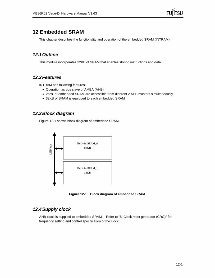
12-1
MB86R02 ‘Jade-D’ Hardware Manual V1.63
12 Embedded SRAM This chapter describes the functionality and operation of the embedded SRAM (INTRAM).
12.1 Outline
This module incorporates 32KB of SRAM that enables storing instructions and data.
12.2 Features
INTRAM has following features: Operation as bus slave of AMBA (AHB) 2pcs. of embedded SRAM are accessible from different 2 AHB masters simultaneously 32KB of SRAM is equipped to each embedded SRAM
12.3 Block diagram
Figure 12-1 shows block diagram of embedded SRAM.
AH
B b
us
Built-in SRAM_1
32KB
Built-in SRAM_0
32KB
Figure 12-1 Block diagram of embedded SRAM
12.4 Supply clock
AHB clock is supplied to embedded SRAM. Refer to "5. Clock reset generator (CRG)" for frequency setting and control specification of the clock.

13-1
MB86R02 ‘Jade-D’ Hardware Manual V1.63
13 DDR2 Controller This chapter describes function and operation of DDR2 controller (DDR2C).
13.1 Outline
DDR2C adopts AHB bus used in the register access as HOST IF and AXI bus used in the memory access. Memory IF supports DDR2SDRAM (DDR2-400)* * Note: MB86R02 'Jade-D' ES1 only supports DDR2-800 memories.
13.2 Features
DDR2C has following features: a. AHB IF
a) Register access by slave function of AHB IF b) Register setting contents
a- Operation setting of DDR2C
b- Initialization sequence control (DDR IF macro setting, OCD/ODT setting on DDR2C side, SDRAM initialization command issue, and SDRAM control setting)
b. AXI IF a) Storing read/write transactions to internal FIFO by slave function of AHB IF b) Internal FIFO composition
a- Address FIFO: Depth = 8 ~ 28 (controllable with register setting). b- Write data FIFO: Depth = 52 c- Read data FIFO: Depth = 62 d- Read control FIFO: Depth = 28
c. DRAM IF c) 512M bit/256M bit DDR2SDRAM (SSTL18) × 2pcs. (recommended) or 1pc.
(DDR2-400/533/667/800 in compliance with JESD79-2C is used as DDR2-400; in addition, SDRAM with ODT=50Ω setting is recommended.)
d) Switch of initialization mode and normal operation mode e) SDRAM usage restriction (AL = 0, CL = 3, WL = 2, BL = 4, Bank = 4) f) Automatic issuing function of refresh command g) Max. 166MHz of SDRAM CLK (double edge: 333MHz)
13.3 Limitation
Please note that you should not write to or read from memory using the ARM core when the memory has been put into self-refresh mode and the clock is turned off. This could cause the system to hang.
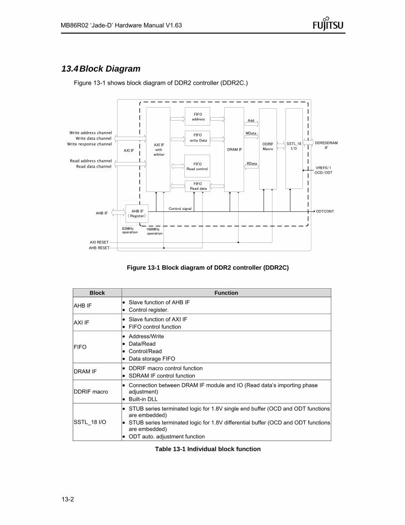
13-2
MB86R02 ‘Jade-D’ Hardware Manual V1.63
13.4 Block Diagram
Figure 13-1 shows block diagram of DDR2 controller (DDR2C.)
AXI IFwith
arbiter
FIFOaddress
DRAM IF
DDRIFMacro
Write address channelWrite data channel
Write response channel
Read address channelRead data channel
FIFORead data
Control signalAHB IF
Add
RData
WData
SSTL_18I/O
operation166MHz
operation83MHz
AXI RESET
AHB RESET
FIFO
write Data
AXI IF
FIFORead control
DDR2SDRAMIF
ODTCONT
VREF0/1OCD/ODT
AHB IF( Register)
Figure 13-1 Block diagram of DDR2 controller (DDR2C)
Block Function
AHB IF Slave function of AHB IF Control register.
AXI IF Slave function of AXI IF FIFO control function
FIFO
Address/Write Data/Read Control/Read Data storage FIFO
DRAM IF DDRIF macro control function SDRAM IF control function
DDRIF macro Connection between DRAM IF module and IO (Read data’s importing phase
adjustment) Built-in DLL
SSTL_18 I/O
STUB series terminated logic for 1.8V single end buffer (OCD and ODT functionsare embedded)
STUB series terminated logic for 1.8V differential buffer (OCD and ODT functionsare embedded)
ODT auto. adjustment function
Table 13-1 Individual block function
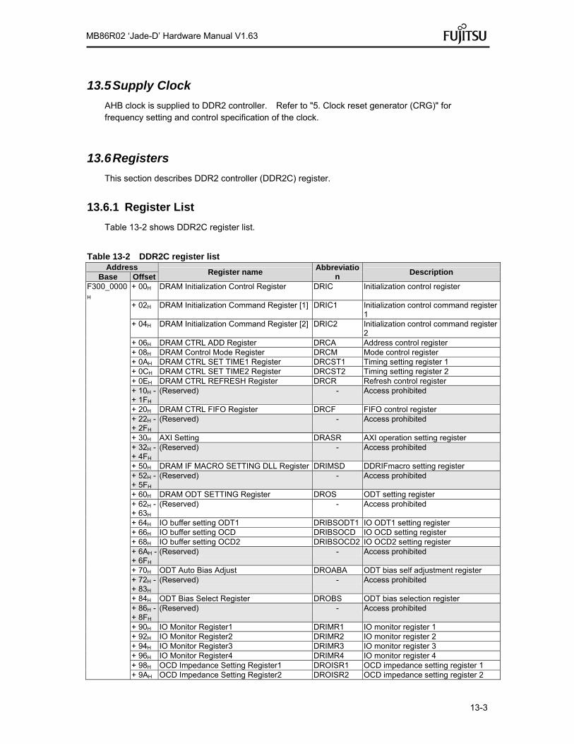
13-3
MB86R02 ‘Jade-D’ Hardware Manual V1.63
13.5 Supply Clock
AHB clock is supplied to DDR2 controller. Refer to "5. Clock reset generator (CRG)" for frequency setting and control specification of the clock.
13.6 Registers
This section describes DDR2 controller (DDR2C) register.
13.6.1 Register List
Table 13-2 shows DDR2C register list.
Table 13-2 DDR2C register list Address
Register name Abbreviatio
n Description
Base Offset F300_0000H
+ 00H DRAM Initialization Control Register DRIC Initialization control register
+ 02H DRAM Initialization Command Register [1] DRIC1 Initialization control command register
1
+ 04H DRAM Initialization Command Register [2] DRIC2 Initialization control command register
2 + 06H DRAM CTRL ADD Register DRCA Address control register + 08H DRAM Control Mode Register DRCM Mode control register + 0AH DRAM CTRL SET TIME1 Register DRCST1 Timing setting register 1 + 0CH DRAM CTRL SET TIME2 Register DRCST2 Timing setting register 2 + 0EH DRAM CTRL REFRESH Register DRCR Refresh control register
+ 10H -
+ 1FH (Reserved) - Access prohibited
+ 20H DRAM CTRL FIFO Register DRCF FIFO control register
+ 22H -
+ 2FH (Reserved) - Access prohibited
+ 30H AXI Setting DRASR AXI operation setting register
+ 32H -
+ 4FH (Reserved) - Access prohibited
+ 50H DRAM IF MACRO SETTING DLL Register DRIMSD DDRIFmacro setting register
+ 52H -
+ 5FH (Reserved) - Access prohibited
+ 60H DRAM ODT SETTING Register DROS ODT setting register
+ 62H -
+ 63H (Reserved) - Access prohibited
+ 64H IO buffer setting ODT1 DRIBSODT1 IO ODT1 setting register + 66H IO buffer setting OCD DRIBSOCD IO OCD setting register + 68H IO buffer setting OCD2 DRIBSOCD2 IO OCD2 setting register
+ 6AH -
+ 6FH (Reserved) - Access prohibited
+ 70H ODT Auto Bias Adjust DROABA ODT bias self adjustment register
+ 72H -
+ 83H (Reserved) - Access prohibited
+ 84H ODT Bias Select Register DROBS ODT bias selection register
+ 86H -
+ 8FH (Reserved) - Access prohibited
+ 90H IO Monitor Register1 DRIMR1 IO monitor register 1 + 92H IO Monitor Register2 DRIMR2 IO monitor register 2 + 94H IO Monitor Register3 DRIMR3 IO monitor register 3 + 96H IO Monitor Register4 DRIMR4 IO monitor register 4 + 98H OCD Impedance Setting Register1 DROISR1 OCD impedance setting register 1 + 9AH OCD Impedance Setting Register2 DROISR2 OCD impedance setting register 2

13-4
MB86R02 ‘Jade-D’ Hardware Manual V1.63
Description format of register Following format is used for description of register’s each bit in "13.6.2 DRAM initialization control register (DRIC)" to "13.6.24 OCD impedance setting register 2 (DROISR2)".
Address Base address + Offset Bit 31 30 29 28 27 26 25 24 23 22 21 20 19 18 17 16
Name R/W
Initial value Bit 15 14 13 12 11 10 9 8 7 6 5 4 3 2 1 0
Name R/W
Initial value
Meaning of item and sign Address
Address (base address + offset address) of the register Bit
Bit number of the register Name
Bit field name of the register R/W
Attribution of read/write of each bit field R0:Read value is always "0" R1: Read value is always "1" W0: Write value is always "0", and write access of "1" is ignored W1: Write value is always "1", and write access of "0" is ignored R: Read W: Write Initial value
Each bit field’s value after reset 0: Value is "0" 1: Value is "1" X: Value is undefined
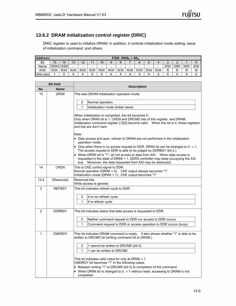
13-5
MB86R02 ‘Jade-D’ Hardware Manual V1.63
13.6.2 DRAM initialization control register (DRIC)
DRIC register is used to initialize DRAM; in addition, it controls initialization mode setting, issue of initialization command, and others.
Address F300_0000H + 00H
Bit 15 14 13 12 11 10 9 8 7 6 5 4 3 2 1 0 Name DRINI CKEN - - - - - - - - - - REFBSY DDRBSY CMDRDY DRCMD R/W R/W R/W R/W R/W R/W R/W R/W R/W R/W R/W R/W R/W R R R W
Initial value 1 0 X X X X X X X X X X X X X X
Bit field
Description No. Name
15 DRINI This sets DRAM initialization operation mode.
0 Normal operation
1 Initialization mode (Initial value) When initialization is completed, this bit becomes 0. Only when DRINI bit is 1, CKEN and DRCMD bits of this register, and DRAM initialization command register [1]/[2] become valid. When this bit is 0, these registers and bits are don’t care. Note: Data access and auto. refresh to DRAM are not performed in the initialization
operation mode. Only when there is no access request to DDR, DRINI bit can be changed to 0 1.
The access request to DDR is able to be judged by DDRBSY (bit 2.) When DRINI bit is "1", do not access to data from AXI. When data access is
requested in the state of DRINI = 1, DDR2 controller may keep occupying the AXI bus. Moreover, the data requested from AXI may be destroyed.
14 CKEN This is CKE control signal to DDR. Normal operation (DRINI = 0): CKE output always becomes "1" Initialization mode (DRINI = 1): CKE output becomes "1"
13-4 (Reserved) Reserved bits. Write access is ignored.
3 REFBSY This bit indicates refresh cycle to DDR.
0 It is not refresh cycle
1 It is refresh cycle
2 DDRBSY This bit indicates status that data access is requested to DDR.
0 Neither command request to DDR nor access to DDR occurs
1 Command request to DDR or access operation to DDR occurs (busy)
1 CMDRDY This bit indicates DRAM command is ready. It also shows whether "1" is able to be written to DRCMD bit (writing command bit to DRAM.)
0 1 cannot be written to DRCMD (bit 0)
1 1 can be written to DRCMD This bit indicates valid value for only at DRINI = 1. CMDRDY bit becomes "1" in the following cases: Between writing "1" to DRCMD (bit 0) to completion of the command. When DRINI bit is changed to 0 1 without reset, accessing to DRAM is not
completed.

13-6
MB86R02 ‘Jade-D’ Hardware Manual V1.63
Bit field Description
No. Name
0 DRCMD This is writing command bit to DRAM. Writing "1" to this bit outputs setting condition of DRAM initialization command register [1]/[2] to DRAM during 1ck period of time. Note: When DRCMD bit does not issue command in the initialization mode, the state
becomes NOP or DSEL to DRAM. Only when CMDBSY (bit 1) is "0", "1" is able to be written to this bit.

13-7
MB86R02 ‘Jade-D’ Hardware Manual V1.63
13.6.3 DRAM initialization command register [1] (DRIC1)
This register sets each control signal value of DRAM at the initialization operation. When "1" is written to DRCMD in the initialization mode (DRINI = 1), the signal corresponding to DRAM bus is driven by this setting value.
Address F300_0000H + 02H Bit 15 14 13 12 11 10 9 8 7 6 5 4 3 2 1 0
Name - - - - - - - - - #CS#RA
S #CA
S #WE BA2 BA1 BA0
R/W R/W R/W R/W R/W R/W R/W R/W R/W R/W R/W R/W R/W R/W R/W R/W R/WInitial value X X X X X X X X X 1 1 1 1 1 1 1
13.6.4 DRAM initialization command register [2] (DRIC2)
This register sets DRAM address signal value at the initialization operation. When "1" is written to DRCMD in the initialization mode (DRINI = 1), the signal corresponding to DRAM bus is driven by this setting value.
Address F300_0000H + 04H Bit 15 14 13 12 11 10 9 8 7 6 5 4 3 2 1 0
Name A15 A14 A13 A12 A11 A10 A9 A8 A7 A6 A5 A4 A3 A2 A1 A0 R/W R/W R/W R/W R/W R/W R/W R/W R/W R/W R/W R/W R/W R/W R/W R/W R/W
Initial value 0 0 0 0 0 0 0 0 0 0 0 0 0 0 0 0
DRAM initialization method All DRAM is initialized by CPU. DDR2 controller is structured that each signal conductor necessary for the DRAM setting can be driven by the register value in the initialization mode. Set certain value to this register beforehand and "1" to command bit (DRCMD) to execute the setting command to DRAM.
To issue "Precharge all (PALL)" command to DRAM 1) Set "Bit[5:0] = 001000(b)" to DRAM initialization command register [1]. 2) Set "Bit[13:0] = 00010000000000(b)" to DRAM initialization command register [2].
(Setting order of these 2 registers is not specified.) 3) Write "1" to bit 0 of DRAM initialization control register.
The value set at 1) and 2) is output to DRAM for 1ck period of time, and this becomes command to DRAM.
Command to DRAM without command execution in the initialization mode is NOP or DSEL
For each control method of DRAM command and initialization, refer applied DRAM data sheet.
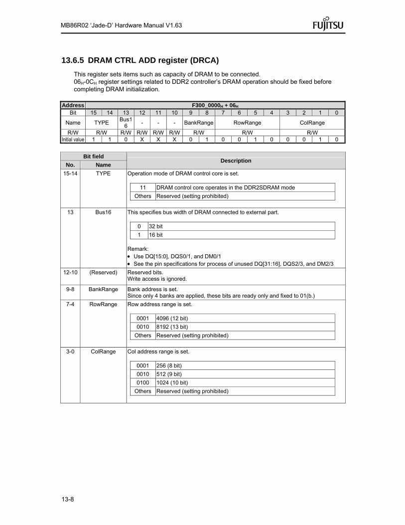
13-8
MB86R02 ‘Jade-D’ Hardware Manual V1.63
13.6.5 DRAM CTRL ADD register (DRCA)
This register sets items such as capacity of DRAM to be connected. 06H-0CH register settings related to DDR2 controller’s DRAM operation should be fixed before completing DRAM initialization.
Address F300_0000H + 06H
Bit 15 14 13 12 11 10 9 8 7 6 5 4 3 2 1 0
Name TYPE Bus1
6 - - - BankRange RowRange ColRange
R/W R/W R/W R/W R/W R/W R/W R/W R/W Initial value 1 1 0 X X X 0 1 0 0 1 0 0 0 1 0
Bit field
Description No. Name
15-14 TYPE Operation mode of DRAM control core is set.
11 DRAM control core operates in the DDR2SDRAM mode
Others Reserved (setting prohibited)
13 Bus16 This specifies bus width of DRAM connected to external part.
0 32 bit
1 16 bit Remark: Use DQ[15:0], DQS0/1, and DM0/1 See the pin specifications for process of unused DQ[31:16], DQS2/3, and DM2/3
12-10 (Reserved)
Reserved bits. Write access is ignored.
9-8 BankRange Bank address is set. Since only 4 banks are applied, these bits are ready only and fixed to 01(b.)
7-4 RowRange Row address range is set.
0001 4096 (12 bit)
0010 8192 (13 bit)
Others Reserved (setting prohibited)
3-0 ColRange Col address range is set.
0001 256 (8 bit)
0010 512 (9 bit)
0100 1024 (10 bit)
Others Reserved (setting prohibited)
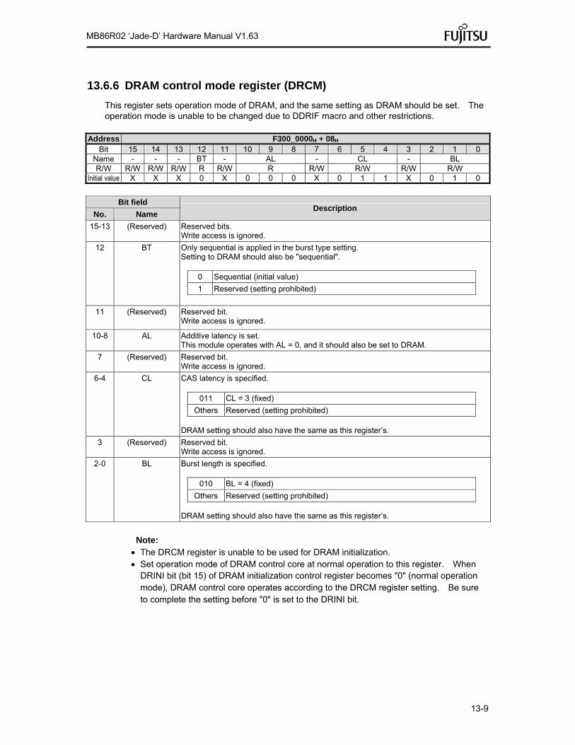
13-9
MB86R02 ‘Jade-D’ Hardware Manual V1.63
13.6.6 DRAM control mode register (DRCM)
This register sets operation mode of DRAM, and the same setting as DRAM should be set. The operation mode is unable to be changed due to DDRIF macro and other restrictions.
Address F300_0000H + 08H Bit 15 14 13 12 11 10 9 8 7 6 5 4 3 2 1 0
Name - - - BT - AL - CL - BL R/W R/W R/W R/W R R/W R R/W R/W R/W R/W
Initial value X X X 0 X 0 0 0 X 0 1 1 X 0 1 0
Bit field
Description No. Name
15-13 (Reserved) Reserved bits. Write access is ignored.
12 BT Only sequential is applied in the burst type setting. Setting to DRAM should also be "sequential".
0 Sequential (initial value)
1 Reserved (setting prohibited)
11 (Reserved)
Reserved bit. Write access is ignored.
10-8 AL Additive latency is set. This module operates with AL = 0, and it should also be set to DRAM.
7 (Reserved) Reserved bit. Write access is ignored.
6-4 CL CAS latency is specified.
011 CL = 3 (fixed)
Others Reserved (setting prohibited) DRAM setting should also have the same as this register’s.
3 (Reserved) Reserved bit. Write access is ignored.
2-0 BL Burst length is specified.
010 BL = 4 (fixed)
Others Reserved (setting prohibited) DRAM setting should also have the same as this register’s.
Note: The DRCM register is unable to be used for DRAM initialization. Set operation mode of DRAM control core at normal operation to this register. When
DRINI bit (bit 15) of DRAM initialization control register becomes "0" (normal operation mode), DRAM control core operates according to the DRCM register setting. Be sure to complete the setting before "0" is set to the DRINI bit.

13-10
MB86R02 ‘Jade-D’ Hardware Manual V1.63
13.6.7 DRAM CTRL SET TIME1 Register (DRCST1)
This register sets access timing to DRAM. It should be set with correlation of internal clock frequency and DRAM spec to be used.
Address F300_0000H + 0AH Bit 15 14 13 12 11 10 9 8 7 6 5 4 3 2 1 0
Name - TRCD - TRAS - TRP TRC R/W R/W R/W R/W R/W R/W R/W R/W
Initial value X 1 1 1 X 1 1 1 X 1 1 1 1 1 1 1
Bit field
Description No. Name
15 (Reserved) Reserved bit. Write access is ignored.
14-12 TRCD RAS to CAS delay time (rRCD : Active to read or write command delay)
Bit[14:12] Delay time (number of clock)
000 - Reserved (Setting prohibited) 001 -
010 2 011 3 100 4 101 5 110 6 111 7 (Initial value)
11 (Reserved) Reserved bit. Write access is ignored.
10-8 TRAS RAS active time (rRAS : Active to precharge command)
Bit[10:8] Delay time (number of clock)
000 - Reserved (Setting prohibited)
001 5 010 6 011 7 (Note 1) 100 8 101 9 110 10 111 11 (Initial value) Note 1: When 7 or less value is set, writing to DRAM is performed with tRAS
= 8
7 (Reserved) Reserved bit. Write access is ignored.

13-11
MB86R02 ‘Jade-D’ Hardware Manual V1.63
Bit field Description
No. Name
6-4 TRP Precharge time (tRP : Precharge period)
Bit[6:4] Delay time (number of clock)
000 - Reserved (Setting prohibited)
001 3 010 4 011 5 100 6 101 7 110 8 111 9 (Initial value)
3-0 TRC RAS cycle time (tRC : Active to active/Auto. refresh command time)
Bit[3:0] Delay time (number of clock) 0000 - Reserved
(Setting prohibited) 0001 - 0010 - 0011 - 0100 - 0101 - 0110 8 0111 9 1000 10 (Note 1) 1001 11 1010 12 1011 13 1100 14 1101 15 1110 16 1111 17 (Initial value) Note 1: When 10 or less value is set, writing to DRAM is performed with
tRAS = 11 For ACT command interval, larger value of either rRC and rRAS+rRP+tWR is used.
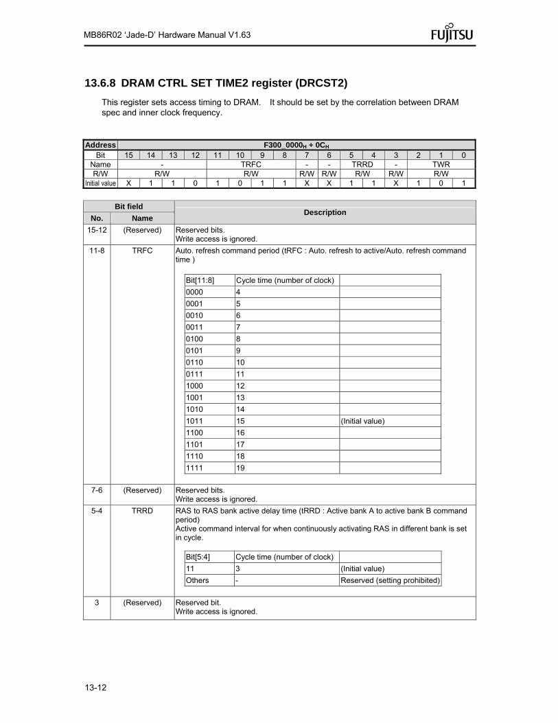
13-12
MB86R02 ‘Jade-D’ Hardware Manual V1.63
13.6.8 DRAM CTRL SET TIME2 register (DRCST2)
This register sets access timing to DRAM. It should be set by the correlation between DRAM spec and inner clock frequency.
Address F300_0000H + 0CH
Bit 15 14 13 12 11 10 9 8 7 6 5 4 3 2 1 0 Name - TRFC - - TRRD - TWR R/W R/W R/W R/W R/W R/W R/W R/W
Initial value X 1 1 0 1 0 1 1 X X 1 1 X 1 0 1
Bit field
Description No. Name
15-12 (Reserved) Reserved bits. Write access is ignored.
11-8 TRFC Auto. refresh command period (tRFC : Auto. refresh to active/Auto. refresh command time )
Bit[11:8] Cycle time (number of clock)
0000 4
0001 5
0010 6
0011 7
0100 8
0101 9
0110 10
0111 11
1000 12
1001 13
1010 14
1011 15 (Initial value)
1100 16
1101 17
1110 18
1111 19
7-6 (Reserved) Reserved bits. Write access is ignored.
5-4 TRRD RAS to RAS bank active delay time (tRRD : Active bank A to active bank B command period) Active command interval for when continuously activating RAS in different bank is set in cycle.
Bit[5:4] Cycle time (number of clock)
11 3 (Initial value)
Others - Reserved (setting prohibited)
3 (Reserved)
Reserved bit. Write access is ignored.

13-13
MB86R02 ‘Jade-D’ Hardware Manual V1.63
Bit field Description
No. Name
2-0 TWR Write recovery time (tWR : Write recovery time) Write recovery time of DRAM is set in cycle.
Bit[2:0] Cycle time (number of clock)
000 - Reserved (setting prohibited)
001 2
010 3
011 4
100 5
101 6 (Initial value)
110 - Reserved (setting prohibited) 111 -

13-14
MB86R02 ‘Jade-D’ Hardware Manual V1.63
13.6.9 DRAM CTRL REFRESH register (DRCR)
This register sets auto. refresh occurrence interval to DRAM. After changing this register value, refresh occurs irregularly.
Address F300_0000H + 0EH
Bit 15 14 13 12 11 10 9 8 7 6 5 4 3 2 1 0 Name - - - - - - - CNTLD REF_CNT R/W R/W R/W R/W R/W R/W R/W R/W R/W R/W
Initial value X X X X X X X 0 0 0 0 0 0 0 0 0
Bit field
Description No. Name
15-9 (Reserved) Reserved bits. Write access is ignored.
8 CNTLD Counter load. REF_CNT value is forcibly loaded into internal counter. When this bit is set to 0 1, REF_CNT value of bit[7:0] is forcibly loaded into internal refresh counter. This is used when setting value needs to be applied, such as after REF_CNT value change. This bit does not need to be rewritten to 0 immediately after loaded because it is performed after detecting the bit change. However, this bit keeps the writing value. If bit value is not 0 at executing load operation, "1" should be written after writing "0". Although CNTLD is not used after REF_CNT change, it operates with the changed REF_CNT by having the period before setting REF_CNT.
7-0 REF_CNT Refresh count. Auto. refresh request occurrence is set in 16 cycle.
00H Refresh request is continuously issued. Priority of refresh is higher than the read/write. Although access request to DRAM occurs, only refresh occurs with this setting.
01H - FFH Refresh request occurs in REF_CNT 16 clock interval. If DRAM data is accessed at refresh request, refresh does not start until the access is completed.
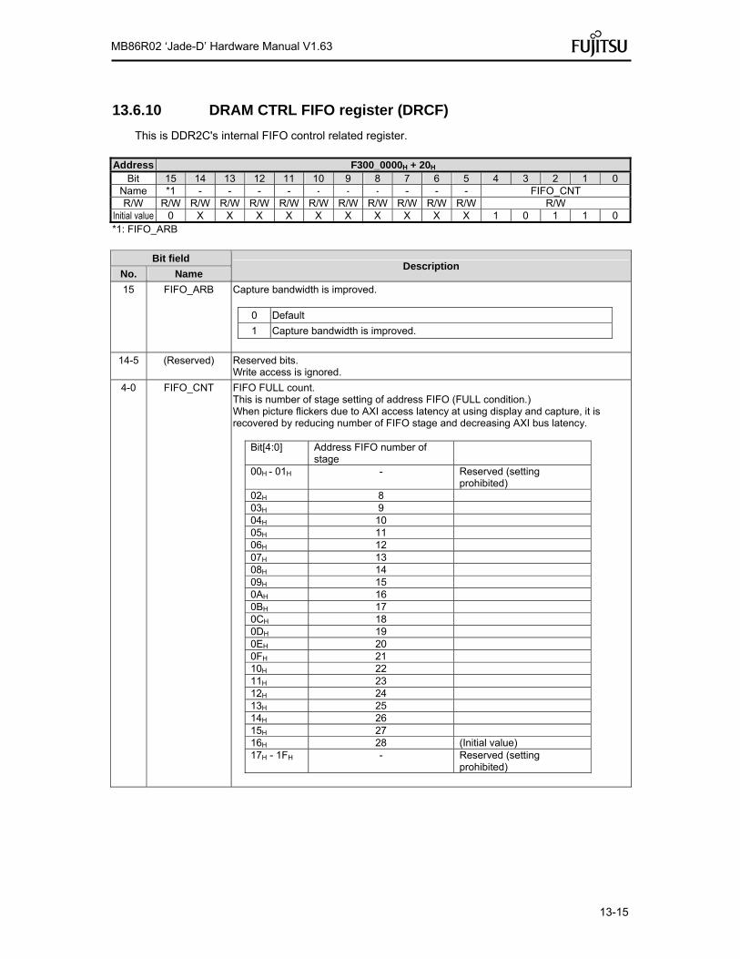
13-15
MB86R02 ‘Jade-D’ Hardware Manual V1.63
13.6.10 DRAM CTRL FIFO register (DRCF)
This is DDR2C's internal FIFO control related register.
Address F300_0000H + 20H Bit 15 14 13 12 11 10 9 8 7 6 5 4 3 2 1 0
Name *1 - - - - - - - - - - FIFO_CNT R/W R/W R/W R/W R/W R/W R/W R/W R/W R/W R/W R/W R/W
Initial value 0 X X X X X X X X X X 1 0 1 1 0 *1: FIFO_ARB
Bit field Description
No. Name
15 FIFO_ARB Capture bandwidth is improved.
0 Default
1 Capture bandwidth is improved.
14-5 (Reserved) Reserved bits. Write access is ignored.
4-0 FIFO_CNT FIFO FULL count. This is number of stage setting of address FIFO (FULL condition.) When picture flickers due to AXI access latency at using display and capture, it is recovered by reducing number of FIFO stage and decreasing AXI bus latency.
Bit[4:0] Address FIFO number of stage
00H - 01H - Reserved (setting prohibited)
02H 8 03H 9 04H 10 05H 11 06H 12 07H 13 08H 14 09H 15 0AH 16 0BH 17 0CH 18 0DH 19 0EH 20 0FH 21 10H 22 11H 23 12H 24 13H 25 14H 26 15H 27 16H 28 (Initial value) 17H - 1FH - Reserved (setting
prohibited)

13-16
MB86R02 ‘Jade-D’ Hardware Manual V1.63
13.6.11 AXI setting register (DRASR)
This register sets AXI interface operation.
Address F300_0000H + 30H Bit 15 14 13 12 11 10 9 8 7 6 5 4 3 2 1 0
Name - - - - - - - - - - - - - - - CACHER/W R/W R/W R/W R/W R/W R/W R/W R/W R/W R/W R/W R/W R/W R/W R/W R/W
Initial value X X X X X X X X X X X X X X X 0
Bit field
Description No. Name
15-1 (Reserved) Reserved bits. Write access is ignored.
0 CACHE CACHE On/Off of cash operation at reading are performed.
0 Cache off (initial value)
1 Cache on When single reading continuously occurs in a single access (16 byte) to DRAM, reading operation from AXI is enabled by the cached data in AXI module instead of accessing to DRAM. However cache is cleared in the following conditions. Burst reading access occurs to AXI bus in DDR2C Write access occurs to AXI bus in DR2C

13-17
MB86R02 ‘Jade-D’ Hardware Manual V1.63
13.6.12 DRAM IF MACRO SETTING DLL register (DRIMSD)
This register is for DDR2-SDRAM interface macro setting which drives macro pin corresponding to each bit by the setting value. This is also for DLL timing setting.
Address F300_0000H + 50H Bit 15 14 13 12 11 10 9 8 7 6 5 4 3 2 1 0
Name - ISFT_3[2:0] - ISFT_2[2:0] - ISFT_1[2:0] - ISFT_0[2:0] R/W R/W R/W R/W R/W R/W R/W R/W R/W
Initial value X 1 1 0 X 1 1 0 X 1 1 0 X 1 1 0
Bit field
Description No. Name
15 (Reserved) Reserved bit. Write access is ignored.
14-12 ISFT_3[2:0] Value of ISFT_3[2:0]
110 (Initial value)
101 Normal operation setting value (set to 101 at DRAM initialization)
Others Reserved (setting prohibited)
11 (Reserved) Reserved bit. Write access is ignored.
10-8 ISFT_2[2:0] Value of ISFT_2[2:0]
110 (Initial value)
101 Normal operation setting value (set to 101 at DRAM initialization)
Others Reserved (setting prohibited)
7 (Reserved) Reserved bit. Write access is ignored.
6-4 ISFT_1[2:0] Value of ISFT_1[2:0]
110 (Initial value)
101 Normal operation setting value (set to 101 at DRAM initialization)
Others Reserved (setting prohibited)
3 (Reserved) Reserved bit. Write access is ignored.
2-0 ISFT_0[2:0] Value of ISFT_0[2:0]
110 (Initial value)
101 Normal operation setting value (set to 101 at DRAM initialization)
Others Reserved (setting prohibited)
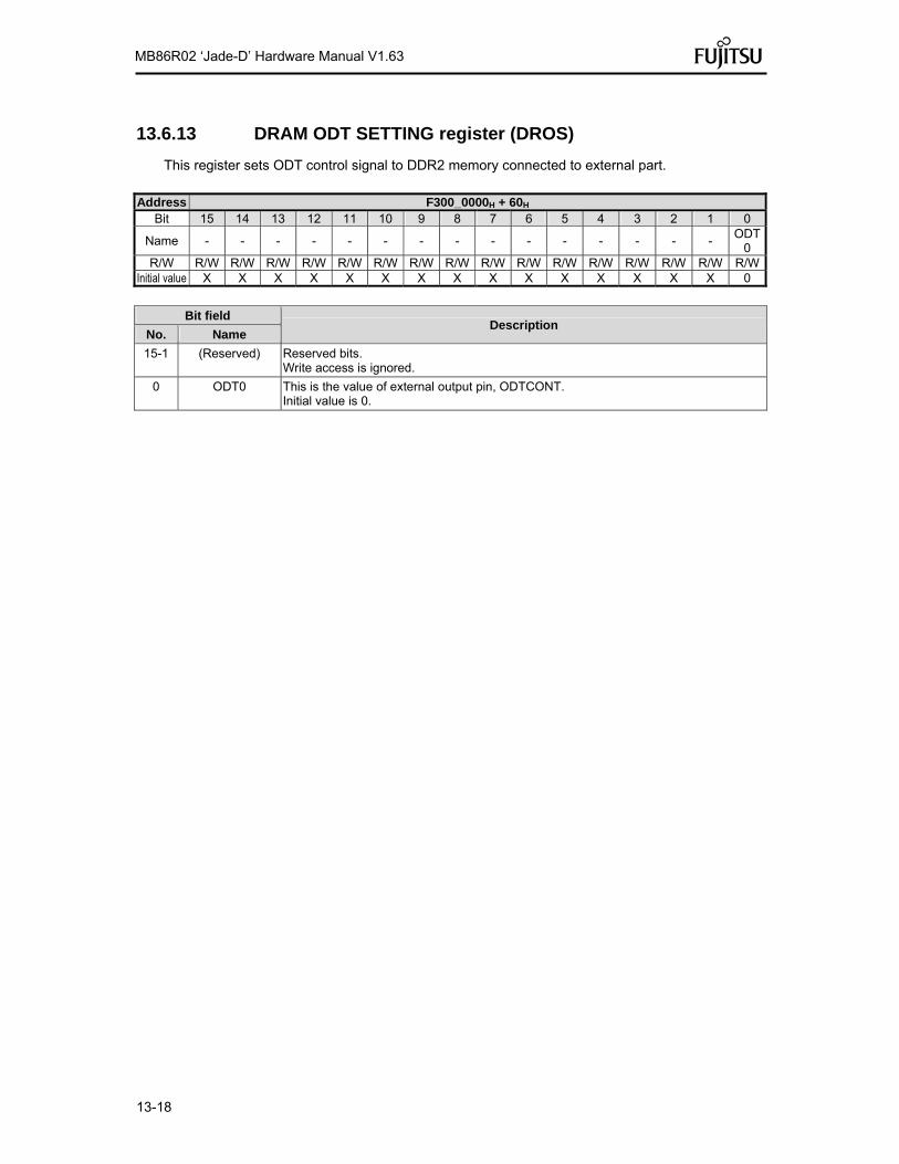
13-18
MB86R02 ‘Jade-D’ Hardware Manual V1.63
13.6.13 DRAM ODT SETTING register (DROS)
This register sets ODT control signal to DDR2 memory connected to external part.
Address F300_0000H + 60H Bit 15 14 13 12 11 10 9 8 7 6 5 4 3 2 1 0
Name - - - - - - - - - - - - - - - ODT
0 R/W R/W R/W R/W R/W R/W R/W R/W R/W R/W R/W R/W R/W R/W R/W R/W R/W
Initial value X X X X X X X X X X X X X X X 0
Bit field
Description No. Name
15-1 (Reserved) Reserved bits. Write access is ignored.
0 ODT0 This is the value of external output pin, ODTCONT. Initial value is 0.

13-19
MB86R02 ‘Jade-D’ Hardware Manual V1.63
13.6.14 IO buffer setting ODT1 (DRIBSODT1)
ODT related setting of IO buffer is set.
Address F300_0000H + 64H Bit 15 14 13 12 11 10 9 8 7 6 5 4 3 2 1 0
Name - - - - - - - - - - ZSELN ODTONN ZSELP ODTONP ZSEL ODTONR/W R/W R/W R/W R/W R/W R/W R/W R/W R/W R/W R/W R/W R/W R/W R/W R/W
Initial value X X X X X X X X X X 0 0 0 0 0 0
Bit field
Description No. Name
15-6 (Reserved) Reserved bits. Write access is ignored.
5 ZSELN This becomes ZSELN value of IO buffer, and this is ODT resistance setting for DQSN.
0 150or 100 (initial value)
1 75 or 50
4 ODTONN This is ODT setting for DQS’s IO, and controls ODTONN of the IO buffer. Initial value is 0.
0 IO buffer’s ODTON is always "0"
1 This should be set to use ODT of IO buffer ODTON is set to off in the following case: To adjust OCD
3 ZSELP This becomes ZSELP value of the IO buffer, and it is ODT resistance setting of DQSP’s IO.
0 150or 100 (initial value)
1 75 or 50
2 ODTONP This is ODT setting of DQS’s IO, and controls ODTONP of the IO buffer. Initial value is 0.
0 IO buffer’s ODTON is always "0"
1 This should be set to use ODT of IO buffer ODTON is set to off in the following case: To adjust OCD
1 ZSEL This is ZSEL value of the IO buffer that is ODT resistance of IO for DQ and DM.
0 150or 100 (initial value)
1 75 or 50
0 ODTON This is ODT setting of IO for DQ and DM, and controls ODTON of IO buffer. Initial value is 0.
0 IO buffer’s ODTON is always "0"
1 This should be set to use ODT of IO buffer ODTON is set to off in the following case: To adjust OCD

13-20
MB86R02 ‘Jade-D’ Hardware Manual V1.63
13.6.15 IO buffer setting OCD (DRIBSOCD)
Each setting used at impedance adjustment of IO buffer is proceeded.
Address F300_0000H + 66H Bit 15 14 13 12 11 10 9 8 7 6 5 4 3 2 1 0
Name - - - - - - - - - - - AFORCE ADRV OCDPOL DIMMCAL OCDCNT R/W R/W R/W R/W R/W R/W R/W R/W R/W R/W R/W R/W R/W R/W R/W R/W R/W
Initial value X X X X X X X X X X X 0 0 0 0 0
Bit field
Description No. Name
15-5 (Reserved) Reserved bits. Write access is ignored.
4 AFORCE This is control bit to switch IO driver's A input, and "1" is set at impedance adjustment. Initial value is 0. When this bit is "1", ADRV bit value of bit 3 is added to driver input A of IO buffer. Be sure to set "0" at the normal operation.
3 ADRV This bit combines with AFORCE of bit 4 to use. When AFORCE is "1", this bit value becomes IO driver's A input. When AFORCE is 0, it is don't care.
2 OCDPOL This becomes OCDPOL value of IO buffer. Initial value is 0.
1 DIMMCAL This becomes DIMMCAL value of IO buffer. Initial value is 0.
0 OCDCNT This becomes OCDCNT value of IO buffer. Initial value is 0.

13-21
MB86R02 ‘Jade-D’ Hardware Manual V1.63
13.6.16 IO buffer setting OCD2 (DRIBSOCD2)
Each setting used at IO buffer’s impedance adjustment is proceeded.
Address F300_0000H + 68H Bit 15 14 13 12 11 10 9 8 7 6 5 4 3 2 1 0
Name - - - - - - - - - - - - - SUSP
D SUSP
R SSEL
R/W R/W R/W R/W R/W R/W R/W R/W R/W R/W R/W R/W R/W R/W R/W R/W R/WInitial value X X X X X X X X X X X X X 0 0 0
Bit field
Description No. Name
15-3 (Reserved)
Reserved bits. Write access is ignored.
2 SUSPD SUSPD setting of IO buffer. When SSEL = 1, this bit value is supplied to SUSPD of each IO buffer.
1 SUSPR SUSPR setting of IO buffer. When SSEL = 1, this bit value is supplied to SUSPR of each IO buffer.
0 SSEL This is selection bit whether to use value of bit1 or bit2 for SUSPR/SUSPD or to control at the internal logic
0 Setting at normal operation DDRIF controls SUSPR/SUSPD
1 Setting value of bit1 and bit2 is used to SUSPR/SUSPD
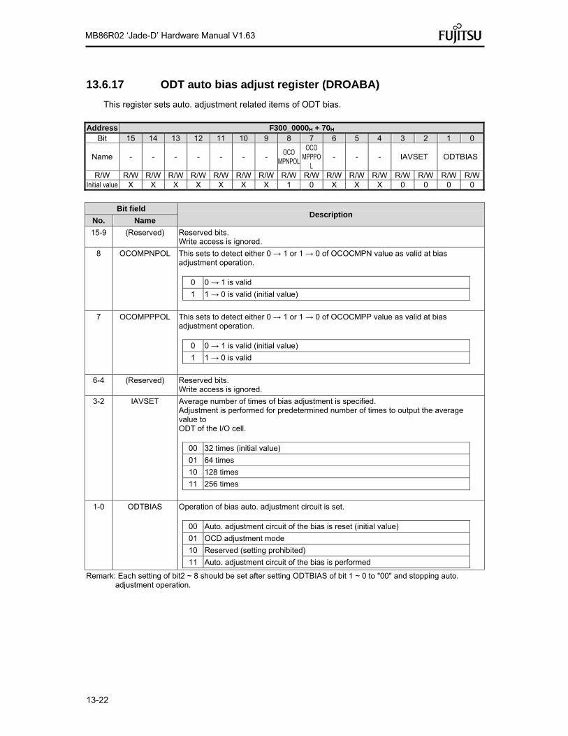
13-22
MB86R02 ‘Jade-D’ Hardware Manual V1.63
13.6.17 ODT auto bias adjust register (DROABA)
This register sets auto. adjustment related items of ODT bias.
Address F300_0000H + 70H Bit 15 14 13 12 11 10 9 8 7 6 5 4 3 2 1 0
Name - - - - - - - OCO
MPNPOL
OCOMPPPO
L - - - IAVSET ODTBIAS
R/W R/W R/W R/W R/W R/W R/W R/W R/W R/W R/W R/W R/W R/W R/W R/W R/WInitial value X X X X X X X 1 0 X X X 0 0 0 0
Bit field
Description No. Name
15-9 (Reserved) Reserved bits. Write access is ignored.
8 OCOMPNPOL This sets to detect either 0 → 1 or 1 → 0 of OCOCMPN value as valid at bias adjustment operation.
0 0 → 1 is valid
1 1 → 0 is valid (initial value)
7 OCOMPPPOL This sets to detect either 0 → 1 or 1 → 0 of OCOCMPP value as valid at bias adjustment operation.
0 0 → 1 is valid (initial value)
1 1 → 0 is valid
6-4 (Reserved) Reserved bits. Write access is ignored.
3-2 IAVSET Average number of times of bias adjustment is specified. Adjustment is performed for predetermined number of times to output the average value to ODT of the I/O cell.
00 32 times (initial value)
01 64 times
10 128 times
11 256 times
1-0 ODTBIAS Operation of bias auto. adjustment circuit is set.
00 Auto. adjustment circuit of the bias is reset (initial value)
01 OCD adjustment mode
10 Reserved (setting prohibited)
11 Auto. adjustment circuit of the bias is performed
Remark: Each setting of bit2 ~ 8 should be set after setting ODTBIAS of bit 1 ~ 0 to "00" and stopping auto. adjustment operation.

13-23
MB86R02 ‘Jade-D’ Hardware Manual V1.63
13.6.18 ODT bias select register (DROBS)
This register sets ODT.
Address F300_0000H + 84H Bit 15 14 13 12 11 10 9 8 7 6 5 4 3 2 1 0
Name - - - - - - - - - - - - - - - AUTOR/W R/W R/W R/W R/W R/W R/W R/W R/W R/W R/W R/W R/W R/W R/W R/W R/W
Initial value X X X X X X X X X X X X X X X 0
Bit field
Description No. Name
15-1 (Reserved) Reserved bits. Write access is ignored.
0 AUTO This sets whether to use ODT auto. setting value mode. When it is set, the average value calculated with auto. adjustment of the bias is used to ODT value of the I/O cell.
0 The ODT auto. setting value mode is not used
1 The ODT auto. setting value mode is used

13-24
MB86R02 ‘Jade-D’ Hardware Manual V1.63
13.6.19 IO monitor register 1 (DRIMR1)
This is input level monitor of IO buffer which is used for impedance adjustment of OCD.
Address F300_0000H + 90H Bit 15 14 13 12 11 10 9 8 7 6 5 4 3 2 1 0
Name DQX[15:0] R/W R
Initial value X X X X X X X X X X X X X X X X
Bit field
Description No. Name
15-1 DQX[15:1] Reserved Write access is ignored.
0 DQX0 X value of DQ0 can be read.
When input value of IO is read, IO driver should be in the OCD adjustment mode. The following settings are required: Bit 0 of IO buffer setting OCD2 register (68H) is set to "1". Bit 1 of IO buffer setting OCD2 register (68H) is set to "0".
Remark:
Monitor value is valid only at OCD adjustment.
13.6.20 IO monitor register 2 (DRIMR2)
This is input level monitor of IO buffer which is used for impedance adjustment of OCD.
Address F300_0000H + 92H Bit 15 14 13 12 11 10 9 8 7 6 5 4 3 2 1 0
Name DQX[31:16] R/W R
Initial value X X X X X X X X X X X X X X X X
Bit field
Description No. Name
15-0 DQX[31:16] Reserved Write access is ignored.
When input value of IO is read, IO driver should be in the OCD adjustment mode. The following settings are required: Bit 0 of IO buffer setting OCD2 register (68H) is set to "1". Bit 1 of IO buffer setting OCD2 register (68H) is set to "0".
Remark:
Monitor value is valid only at OCD adjustment.

13-25
MB86R02 ‘Jade-D’ Hardware Manual V1.63
13.6.21 IO monitor register 3 (DRIMR3)
This is input level monitor of IO buffer which is used for impedance adjustment of OCD.
Address F300_0000H + 94H Bit 15 14 13 12 11 10 9 8 7 6 5 4 3 2 1 0
Name DQSX[15:0] R/W R
Initial value X X X X X X X X X X X X X X X X
Bit field
Description No. Name
15-0 (Reserved) Reserved bits. Write access is ignored.
When input value of IO is read, IO driver should be in the OCD adjustment mode. The following settings are required: Bit 0 of IO buffer setting OCD2 register (68H) is set to "1". Bit 1 of IO buffer setting OCD2 register (68H) is set to "0".
Remark:
Monitor value is valid only at OCD adjustment.
13.6.22 IO monitor register 4 (DRIMR4)
This is input level monitor of IO buffer which is used for impedance adjustment of OCD.
Address F300_0000H + 96H Bit 15 14 13 12 11 10 9 8 7 6 5 4 3 2 1 0
Name DMX[15:0] R/W R
Initial value X X X X X X X X X X X X X X X X
Bit field Description
No. Name
15-0 (Reserved) Reserved bits. Write access is ignored.
When input value of IO is read, IO driver should be in the OCD adjustment mode. The following settings are required: Bit 0 of IO buffer setting OCD2 register (68h) is set to "1". Bit 1 of IO buffer setting OCD2 register (68h) is set to "0".
Remark:
Monitor value is valid only at OCD adjustment.

13-26
MB86R02 ‘Jade-D’ Hardware Manual V1.63
13.6.23 OCD impedance setting register 1 (DROISR1)
This register sets impedance adjustment value.
Address F300_0000H + 98H Bit 15 14 13 12 11 10 9 8 7 6 5 4 3 2 1 0
Name DRVN2 DRVP2 DRVN1 DRVP1 R/W R/W R/W R/W R/W
Initial value 0 1 0 0 1 0 0 1 0 1 0 0 1 0 0 1
Bit field
Description No. Name
15-12 DRVN2 This register sets DRVN value of DQ[15:8], DQS1, and DM1
11-8 DRVP2 This register sets DRVP value of DQ[15:8], DQS1, and DM1
7-4 DRVN1 This register sets DRVN value of DQ[7:0], DQS0, and DM0
3-0 DRVP1 This register sets DRVP value of DQ[7:0], DQS0, and DM0
13.6.24 OCD impedance setting register 2 (DROISR2)
This register sets impedance adjustment value.
Address F300_0000H + 9AH
Bit 15 14 13 12 11 10 9 8 7 6 5 4 3 2 1 0 Name DRVN4 DRVP4 DRVN3 DRVP3 R/W R/W R/W R/W R/W
Initial value 0 1 0 0 1 0 0 1 0 1 0 0 1 0 0 1
Bit field
Description No. Name
15-12 DRVN4 This register sets DRVN value of DQ[31:24], DQS3, and DM3
11-8 DRVP4 This register sets DRVP value of DQ[31:24], DQS3, and DM3
7-4 DRVN3 This register sets DRVN value of DQ[23:16], DQS2, and DM2
3-0 DRVP3 This register sets DRVP value of DQ[23:16], DQS2, and DM2
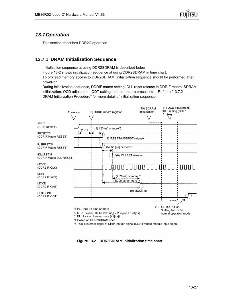
13-27
MB86R02 ‘Jade-D’ Hardware Manual V1.63
13.7 Operation
This section describes DDR2C operation.
13.7.1 DRAM Initialization Sequence
Initialization sequence at using DDR2SDRAM is described below. Figure 13-2 shows initialization sequence at using DDR2SDRAM in time chart. To proceed memory access to DDR2SDRAM, initialization sequence should be performed after power-on. During initialization sequence, DDRIF macro setting, DLL reset release in DDRIF macro, SDRAM initialization, OCD adjustment, ODT setting, and others are processed. Refer to "13.7.2 DRAM Initialization Procedure" for more detail of initialization sequence.
Figure 13-2 DDR2SDRAM initialization time chart
IRESET*5 (DDRIF Macro RESET)
XRST
(CHIP RESET)
IUSRRST*5 (DDRIF Macro RESET)
IDLLRST*5 (DDRIF Macro DLL RESET)
MCKE (DDR2 IF CKE)
*1 PLL lock up time or more
*2 MCKP cycle (166MHz=6[ns]) 20cycle = 120[ns]
MCKP (DDR2 IF CLK)
MCS (DDR2 IF XCS)
*3 DLL lock up time or more (79[us]) *4 Based on DDR2SDRAM spec
ODTCONT (DDR2 IF ODT)
*5 This is internal signal of CHIP, not pin signal (DDRIFmacro module input signal)
Power-on
(1) *1
(6) IDLLRST release
(4) IRESET/IUSRRST release
(2) DDRIF macro register
(3) 120[ns] or more*2
(5) 120[ns] or more*2
(7)79[us] or more *3
(8)200[us] or more *4
(9) MCKE on
(10) SDRAM initialization
(12) ODTCONT-on Shifting to DDR2C normal operation mode
(11) OCD adjustment, ODT setting (CHIP side)

13-28
MB86R02 ‘Jade-D’ Hardware Manual V1.63
13.7.2 DRAM Initialization Procedure
The figure below is a whole flow of the register setting procedure for initialization sequence. Each number matches to the one in DDR2SDRAM initialization time chart shown in Figure 13-2. The procedure showing here is only the register setting relating to the DRAM initialization.
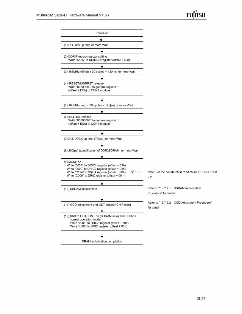
13-29
MB86R02 ‘Jade-D’ Hardware Manual V1.63
(1) PLL lock up time or more Wait
(3) 166MHz (6[ns]) x 20 cycles = 120[ns] or more Wait
(4) IRESET/IUSRRST release Write “00000002” to general register 1 (offset + ECh) of CCNT module
(2) DDRIF macro register setting Write "5555” to DRIMSD register (offset + 50h)
(5) 166MHz([ns]) x 20 cycles = 120[ns] or more Wait
Power-on
(6) IDLLRST release Write “00000003” to general register 1 (offset + ECh) of CCNT module
(7) DLL LOCK up time (79[µs]) or more Wait
(8) 200[µs] (specification of DDR2SDRAM) or more Wait
(9) MCKE on Write “003F” to DRIC1 register (offset + 02h) Write “0000” to DRIC2 register (offset + 04h) Write “C124” to DRCA register (offset + 06h) Write “C000” to DRIC register (offset + 00h)
(10) SDRAM initialization
(11) OCD adjustment and ODT setting (CHIP side)
(12) Shift to ODTCONT on (SDRAM side) and DDR2C normal operation mode Write “0001” to DROS register (offset + 60h) Write “4000” to DRIC register (offset + 00h)
DRAM initialization completion
Refer to "13.7.2.1 SDRAM Initialization
Procedure" for detail
Refer to "13.7.2.2 OCD Adjustment Procedure"
for detail
Note: For the construction of 512M bit DDR2SDRAM
2

13-30
MB86R02 ‘Jade-D’ Hardware Manual V1.63
13.7.2.1 SDRAM Initialization Procedure
The figure below is DDR2SDRAM initialization setting procedure at DRAM initialization. DDR2SDRAM initialization sequence's command contents to be issued may change depending on the memory specification connected to this chip. For each command's issuing contents and DDR2C command issuing timing, be sure to confirm memory spec in use to set properly.

13-31
MB86R02 ‘Jade-D’ Hardware Manual V1.63
Write “C001” to DRIC register (offset + 00h)
START
Write “0017” to DRIC1 register (offset + 02h) Write ”0400” to DRIC2 register (offset + 04h) Write ”C001” to DRIC register (offset + 00h)
Write ”0006” to DRIC1 register (offset + 02h) Write ”0000” to DRIC2 register (offset t+ 04h) Write ”C001” to DRIC register (offset + 00h)
DDR2 IF: Issue NOP command
DDR2 IF: Issue PALL command
DDR2 IF: Issue EMR (2) command
Write ”0007” to DRIC1 register (offset + 02h) Write ”0000” to DRIC2 register (offset + 04h) Write ”C001” to DRIC register (offset + 00h)
DDR2 IF: Issue EMR (3) command
Write ”0005” to DRIC1 register (offset +02h) Write ”0000” to DRIC2 register (offset t+04h) Write ”C001” to DRIC register (offset +00h)
DDR2 IF: Issue EMR (1) command
Write ”0000” to DRIC1 register (offset + 02h) Write ”0532” to DRIC2 register (offset + 04h) Write ”C001” to DRIC register (offset + 00h)
DDR2 IF: Issue MRS command
Write ”0017” to DRIC1 register (offset + 02h) Write ”0400” to DRIC2 register (offset + 04h) Write ”C001” to DRIC register (offset + 00h)
DDR2 IF: Issue PALL command
Write ”000F” to DRIC1 register (offset + 02h) Write ”0000” to DRIC2 register (offset + 04h) Write ”C001” to DRIC register (offset + 00h) Write ”C001” to DRIC register (offset + 00h)
DDR2 IF: Issue 2x REF commands
Write ”0000” to DRIC1 register (offset + 02h) Write ”0432” to DRIC2 register (offset + 04h) Write ”C001” to DRIC register (offset + 00h)
DDR2 IF: Issue MRS command
Write ”0005” to DRIC1 register (offset + 02h) Write ”0380” to DRIC2 register (offset + 04h) Write ”C001” to DRIC register (offset + 00h)
DDR2 IF: Issue EMR (1) command
A To next sheet
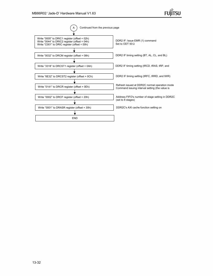
13-32
MB86R02 ‘Jade-D’ Hardware Manual V1.63
END
Write ”0005” to DRIC1 register (offset + 02h) Write ”0044” to DRIC2 register (offset + 04h) Write ”C001” to DRIC register (offset + 00h)
DDR2 IF: Issue EMR (1) command Set to ODT 50Ω
DDR2 IF timing setting (BT, AL, CL, and BL)
A Continued from the previous page
Write ”0032” to DRCM register (offset + 08h)
Write ”3318” to DRCST1 register (offset + 0Ah)
Write ”6E32” to DRCST2 register (offset + 0Ch)
Write ”0141” to DRCR register (offset + 0Eh)
Write ”0002” to DRCF register (offset + 20h)
Write ”0001” to DRASR register (offset + 30h)
DDR2 IF timing setting (tRCD, tRAS, tRP, and
DDR2 IF timing setting (tRFC, tRRD, and tWR)
Refresh issued at DDR2C normal operation mode Command issuing interval setting (the value is
f )
Address FIFO's number of stage setting in DDR2C (set to 8 stages)
DDR2C's AXI cache function setting on

13-33
MB86R02 ‘Jade-D’ Hardware Manual V1.63
13.7.2.2 OCD Adjustment Procedure
The figure below is the OCD adjustment setting procedure of SSTL_18 IO used for the DDR2 SDRSAM interface. The setting adjusts driver output impedance of SSTL_18 IO to the optimum value. The pin for OCD adjustment is MDQ[31:0], MDM[3:0], MDQS[3:0], and MDQSN[3:0], however, only MDQ[0] is tested for adjustment.
START
Write "0000" to DRIBSODT1 register (offset + 64h) Write "001B" to DRIBSOCD register (offset + 66h) Write "0001" to DRIBSOCD2 register (offset + 68h) Write "0081" to DROABA register (offset + 70h)
Write "0F0F ~ 0000" to DROISR1 register (offset + 98h) Write "0F0F ~ 0000" to DROISR2 register (offset + 9Ah)
OCD adjustment mode on Set to driver PMOS adjustment mode
Decrement PMOS driver setting value which is corresponding to the change of DRIMR 1.DQX[0] from "0" to "1" DRVP1/2/3/4 = Decrement to 0 ~ F DRVN1/2/3/4 = 0
Read adjustment level of PMOS driver output impedance from DRIMR1 register
Read DRIMR1 register (offset+90h) Read DRIMR2 register (offset + 92h) Read DRIMR3 register (offset + 94h) Read DRIMR4 register (offset + 96h)
Judge (DRIMR1-4 = all "1")
Write "0X0X ~ FXFX" to DROISR1 register (offset + 98h) Write "0X0X ~ FXFX" to DROISR2 register (offset + 9Ah)
Increment applied NMOS driver setting value until DRIMR1.DQX[0] register changes from "0" to "1" DRVP1/2/3/4 = Retain DRVN1/2/3/4 = Increment to 0 ~ F
Read adjustment level of NMOS driver output impedance from DRIMR1 register
Read DRIMR1 register (offset + 90h)
Judge (DRIMR1.DQX[0] = "0")
Write "0017" to DRIBSOCD register (offset + 66h) Set to driver NMOS adjustment
Write "0000" to DRIBSODT1 register (offset + 64h) Write "0000" to DRIBSOCD register (offset + 66h) Write "0000" to DRIBSOCD2 register (offset + 68h)
OCD adjustment mode off Set to normal driver mode
END
All DRVNx (x=1..4) must have the same value.
For DRVN1/2/3/4 and DRIMR1/2/3/4 registers,
refer Table 13-5 and Table 13-6

13-34
MB86R02 ‘Jade-D’ Hardware Manual V1.63
In order to calibrate DRVPx (x=1..4), decrease the value from 0xf to 0x0 until the DQX[0] bit is "1"; see Table 13-3 and Table 13-4. All DRVPx (x=1..4) must have the same value. In order to calibrate DRVNx (x=1..4), increase the value from 0x0 to 0xf until the DQX[0] bit is "0"; see Table 13-5 and Table 13-6. All DRVNx (x=1..4) must have the same value.
Table 13-3 Correspondence table of DRVP1/2 and DRIMR1/3/4 registers
DROISR1 register DRIMR1 register DRIMR3 register DRIMR4 register
11-8 DRVP2 15-8 DQX[15:8] 1 DQSX[1] 1 DMX[1]
3-0 DRVP1 7-0 DQX[7:0] 0 DQSX[0] 0 DMX[0]
Table 13-4 Correspondence table of DRVP3/4 and DRIMR2/3/4 registers
DROISR1 register DRIMR2 register DRIMR3 register DRIMR4 register
11-8 DRVP4 15-8 DQX[31:24] 3 DQSX[3] 3 DMX[3]
3-0 DRVP3 7-0 DQX[23:16] 2 DQSX[2] 2 DMX[2]
Table 13-5 Correspondence table of DRVN1/2 and DRIMR1/3/4 registers
DROISR2 register DRIMR1 register DRIMR3 register DRIMR4 register
15-12 DRVN2 15-8 DQX[15:8] 1 DQSX[1] 1 DMX[1]
7-4 DRVN1 7-0 DQX[7:0] 0 DQSX[0] 0 DMX[0]
Table 13-6 Correspondence table of DRVN3/4 and DRIMR2/3/4 registers
DROISR2 register DRIMR2 register DRIMR3 register DRIMR4 register
15-12 DRVN4 15-8 DQX[31:24] 3 DQSX[3] 3 DMX[3]
7-4 DRVN3 7-0 DQX[23:16] 2 DQSX[2] 2 DMX[2]
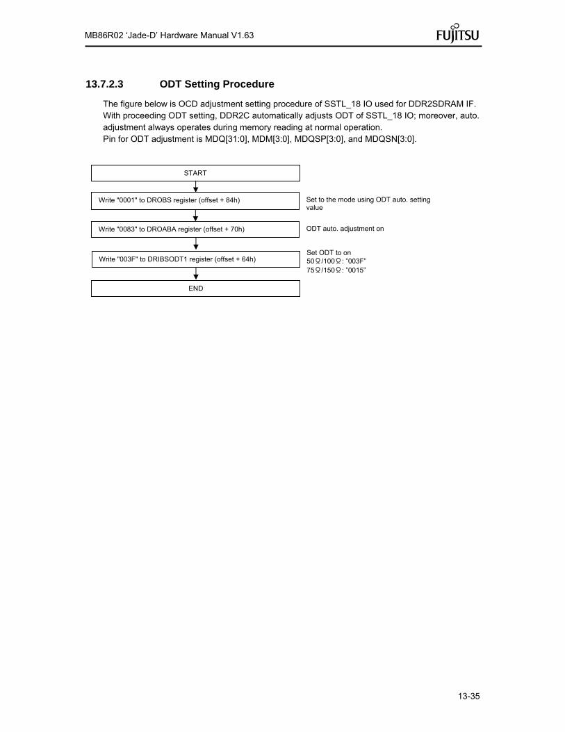
13-35
MB86R02 ‘Jade-D’ Hardware Manual V1.63
13.7.2.3 ODT Setting Procedure
The figure below is OCD adjustment setting procedure of SSTL_18 IO used for DDR2SDRAM IF. With proceeding ODT setting, DDR2C automatically adjusts ODT of SSTL_18 IO; moreover, auto. adjustment always operates during memory reading at normal operation. Pin for ODT adjustment is MDQ[31:0], MDM[3:0], MDQSP[3:0], and MDQSN[3:0].
Write "0001" to DROBS register (offset + 84h)
START
Set to the mode using ODT auto. setting value
ODT auto. adjustment on
Set ODT to on 50Ω/100Ω: ”003F” 75Ω/150Ω: ”0015”
Write "0083" to DROABA register (offset + 70h)
Write "003F" to DRIBSODT1 register (offset + 64h)
END
14-1
MB86R02 ‘Jade-D’ Hardware Manual V1.63
14 Timer (TIMER) This chapter describes function and spec of timer.
14.1 Outline
Timer is 2 channel timer module which is able to set 32/16 bit.
14.2 Feature
Timer has following features: 32/16 bit counter 2 (bit width is controllable with register) Supplying 2 interrupt request signals to interrupt controller Timer clock prescaler unit 3 operation modes:
Free-run mode Cycle timer mode One-shot mode
Using APB clock as base clock of the timer
14.3 Supply clock
APB clock is supplied to timer. Refer to "5. Clock Reset generator (CRG)" for frequency setting and control specification of the clock.
14.4 Specification
Timer in MB86R02 uses ADKr2p0 (AMBA design kit) timer module of ARM Ltd. Refer to Dual input timer of the AMBA Design Kit Technical Reference Manual for detail spec of the timer.

15-1
MB86R02 ‘Jade-D’ Hardware Manual V1.63
15 DMA Controller (DMAC) This chapter describes the functionality and operation of the DMA Controller.
15.1 Outline
The DMAC is an 8-channel DMA controller.
15.2 Feature
DMAC in MB86R02 has following features: Compliant with AMBA v2.0 8 DMA channels DMA trigger
External transfer request (2 channels for external DMA request and 6 channels for I2S transmission/reception DMA requests are available)
Peripheral transfer request (12 types of UART transmission/reception DMA request selectable per channel)
Software request (start-up by register write) Beat transfer
16-word FIFO shared by all channels Supports INCR, INCR 4/8/16, and WRAP 4/8/16.
Transfer modes: Block transfer (I2S: check 'Limitations with I2S' section) Burst transfer (not to I2S!) Demand transfer (not to I2S!)
Programmable 4 bit block register and 16 bit count register Supports 8, 16, and 32 bit transfer widths Supports increment and fixed addressing to source and destination Reload count, source address and destination address register Issues interrupts on errors and completion Displays end code of DMA transfer Supports source and destination protection Hardware support for fixed priority and rotation priority
In fixed priority mode, channel 0 has the highest and channel 7 has the lowest priority
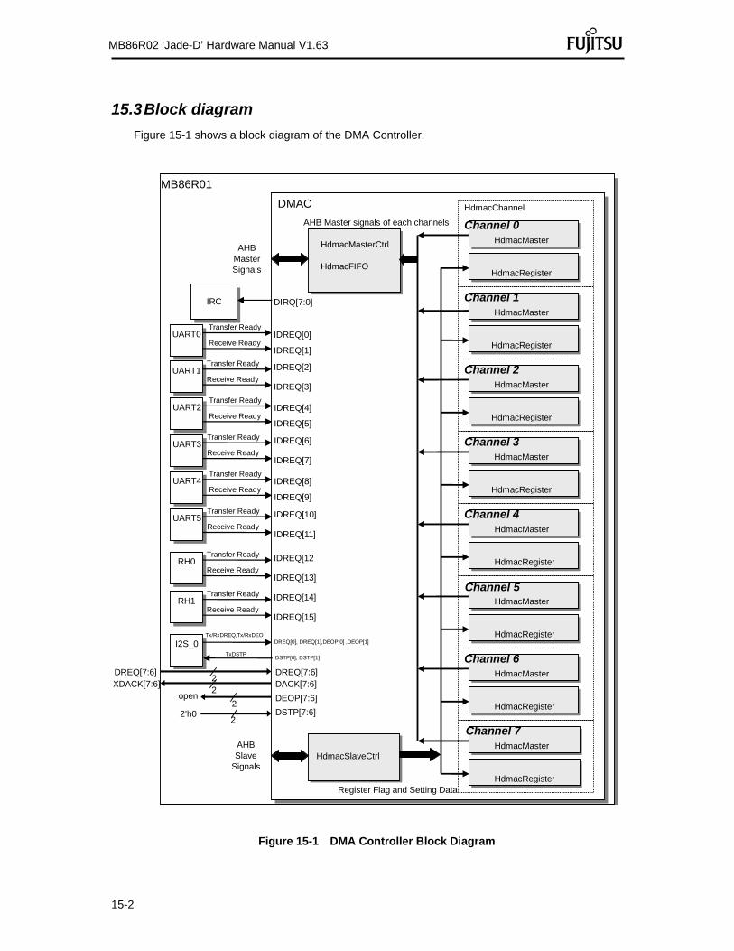
15-2
MB86R02 ‘Jade-D’ Hardware Manual V1.63
15.3 Block diagram
Figure 15-1 shows a block diagram of the DMA Controller.
MB86R01
DMAC
HdmacMasterCtrl HdmacFIFO
AHB Master Signals
HdmacSlaveCtrl AHB Slave
Signals
HdmacMaster
HdmacRegister
HdmacMaster
HdmacRegister
HdmacMaster
HdmacRegister
HdmacMaster
HdmacRegister
HdmacMaster
HdmacRegister
HdmacMaster
HdmacRegister
HdmacMaster
HdmacRegister
HdmacMaster
HdmacRegister
HdmacChannel
Channel 0
Register Flag and Setting Data
AHB Master signals of each channels
Channel 1
Channel 2
Channel 3
Channel 4
Channel 6
Channel 7
IRC DIRQ[7:0]
DREQ[7:6]DREQ[7:6] 2
DACK[7:6] XDACK[7:6] 2
DEOP[7:6]open 2
UART0 IDREQ[0]
IDREQ[1]
Transfer Ready
Receive Ready
UART1 IDREQ[2]
IDREQ[3]
Transfer Ready
Receive Ready
UART2 IDREQ[4]
IDREQ[5]
Transfer Ready
Receive Ready
UART3 IDREQ[6]
IDREQ[7]
Transfer Ready
Receive Ready
UART4 IDREQ[8]
IDREQ[9]
Transfer Ready
Receive Ready
UART5 IDREQ[10]
IDREQ[11]
Transfer Ready
Receive Ready
I2S_0 DREQ[0], DREQ[1],DEOP[0] ,DEOP[1]
DSTP[0], DSTP[1]
Tx/RxDREQ,Tx/RxDEO
TxDSTP
DSTP[7:6] 2
2’h0
Channel 5
RH0 IDREQ[12
IDREQ[13]
Transfer Ready
Receive Ready
RH1 IDREQ[14]
IDREQ[15]
Transfer Ready
Receive Ready
Figure 15-1 DMA Controller Block Diagram

15-3
MB86R02 ‘Jade-D’ Hardware Manual V1.63
Function of the individual blocks Table 15-1 shows each block function of this module.
Table 15-1 Individual block function Block Function
DMAC Most significant module
HdmacMasterCtrl Valid channel selector for priority controller and AHB master transaction
HdmacSlaveCtrl DMAC AHB slave interface controller and valid channel selector I/F for AHB slave transaction
HdmacChannel DMAC 1 channel module DMAC has 8 modules
HdmacMaster DMAC AHB master main controller
HdmacRegister DMAC DMA configuration register controller
HdmacFIFO DMAC 16 word FIFO
15.4 Related pins
MB86R02's DMAC has the following DMA-related pins which are shared with other functions. To use the pins for DMA, the external pins should be set to MPX_MODE_1[1:0] = "HL".
Pin Direction Qty. Description
DREQ[6] DREQ[7]
I 2 DMA request pin which is connected as channel 7 of DMAC and channel 6 of external DREQ signal.
XDACK[6] XDACK[7]
O 2 DMA acknowledge pin which is connected as channel 7 of DMAC and channel 6 of external DACK signal.
15.5 Supply clock
The AHB clock is supplied to the DMA controller. Please refer to "5. Clock reset generator (CRG)" for frequency configuration and the control specifications of this clock.
15-4
MB86R02 ‘Jade-D’ Hardware Manual V1.63
15.6 Registers
This section describes the DMAC register set.
15.6.1 Register list
The DMAC control related registers are shown below.
Module Address Register Function
DMAC common FFFD0000(h) DMACR DMAC configuration register
FFFD0004(h) FFFD000F(h)
Reserved
DMAC ch0 FFFD0010(h) DMACA0 DMAC0 configuration A register
FFFD0014(h) DMACB0 DMAC0 configuration B register
FFFD0018(h) DMACSA0 DMAC0 source address register
FFFD001C(h) DMACDA0 DMAC0 Destination address register
DMAC ch1 FFFD0020(h) DMACA1 DMAC1 configuration A register
FFFD0024(h) DMACB1 DMAC1 configuration B register
FFFD0028(h) DMACSA1 DMAC1 source address register
FFFD002C(h) DMACDA1 DMAC1 Destination address register
DMAC ch2 FFFD0030(h) DMACA2 DMAC2 configuration A register
FFFD0034(h) DMACB2 DMAC2 configuration B register
FFFD0038(h) DMACSA2 DMAC2 source address register
FFFD003C(h) DMACDA2 DMAC2 Destination address register
DMAC ch3 FFFD0040(h) DMACA3 DMAC3 configuration A register
FFFD0044(h) DMACB3 DMAC3 configuration B register
FFFD0048(h) DMACSA3 DMAC3 source address register
FFFD004C(h) DMACDA3 DMAC3 Destination address register
DMAC ch4 FFFD0050(h) DMACA4 DMAC4 configuration A register
FFFD0054(h) DMACB4 DMAC4 configuration B register
FFFD0058(h) DMACSA4 DMAC4 source address register
FFFD005C(h) DMACDA4 DMAC4 Destination address register
DMAC ch5 FFFD0060(h) DMACA5 DMAC5 configuration A register
FFFD0064(h) DMACB5 DMAC5 configuration B register
FFFD0068(h) DMACSA5 DMAC5 source address register
FFFD006C(h) DMACDA5 DMAC5 Destination address register
DMAC ch6 FFFD0070(h) DMACA6 DMAC6 configuration A register
FFFD0074(h) DMACB6 DMAC6 configuration B register
FFFD0078(h) DMACSA6 DMAC6 source address register
FFFD007C(h) DMACDA6 DMAC6 Destination address register
DMAC ch7 FFFD0080(h) DMACA7 DMAC7 configuration A register
FFFD0084(h) DMACB7 DMAC7 configuration B register
FFFD0088(h) DMACSA7 DMAC7 source address register
FFFD008C(h) DMACDA7 DMAC7 Destination address register

15-5
MB86R02 ‘Jade-D’ Hardware Manual V1.63
Notes for setting registers Please note the following when setting DMAC registers. DMACR, DMACA, DMACB, DMACSA and DMACDA registers are accessible in byte, half-
word, and word sizes. Do not set DMAC register address to DMACSA and DMACDA registers. Do not change the settings of a channel's register during DMA transfer except the DE/DH
bits of DMACR and the EB/PB bits of DMACA.
Register description format The following format is used for the description of each register’s bits in "15.6.2 DMA configuration register (DMACR)" to "15.6.6 DMAC destination address register (DMACDAx)".
Address Base address + OffsetBit 31 30 29 28 27 26 25 24 23 22 21 20 19 18 17 16
Name R/W
Initial value Bit 15 14 13 12 11 10 9 8 7 6 5 4 3 2 1 0
Name R/W
Initial value
Meaning of item and sign Address
Address (base address + offset address) of the register Bit
Bit number of the register Name
Bit field name of the register R/W
Attribution of read/write of each bit field R0:Read value is always "0" R1: Read value is always "1" W0: Write value is always "0", and write access of "1" is ignored W1: Write value is always "1", and write access of "0" is ignored R: Read W: Write Initial value
Each bit field’s value after reset 0: Value is "0" 1: Value is "1" X: Value is undefined

15-6
MB86R02 ‘Jade-D’ Hardware Manual V1.63
15.6.2 DMA configuration register (DMACR)
Address FFFD_0000 + 00(h) Bit 31 30 29 28 27 26 25 24 23 22 21 20 19 18 17 16
Name DE DS - PR DH[3:0] (Reserved) R/W R/W R R R/W R/W R/W R/W R/W R R R R R R R R
Initial value 0 0 0 0 0 0 0 0 0 0 0 0 0 0 0 0 Bit 15 14 13 12 11 10 9 8 7 6 5 4 3 2 1 0
Name (Reserved) R/W R R R R R R R R R R R R R R R R
Initial value 0 0 0 0 0 0 0 0 0 0 0 0 0 0 0 0
Bit field
Description No. Name
31 DE (DMA
Enable)
Transfer is controlled for all DMA channels.
0 All DMA channels are disabled and DMA transfer is not performed until "1" is set to this bit If the value is cleared to "0" during the transfer, DMA is stopped at transmission gap for the channel in transfer
1 DMA transfer starts according to the register setting of each channel [Transfer gap] The transfer gap is that DMAC de-asserts bus request (HBUSREQ) to the arbiter during DMA transfer (about 4 clocks) by DMAC. Its occurrence is different by transfer mode shown below.
Block transfer: Transfer gap occurs at BC = 0 (after completing transfer in BC unit) Burst transfer: There is no transfer gap. Demand transfer: Transfer gap occurs at TC = TC - 1 (after completing 1 DMA
transfer), or at transfer request negotiation This bit can be used to reset all channels of Configuration register at a time during DMA transfer.
30 DS (DMA Stop)
This shows all channels of DMA transfer is stop.
0 Release of disable/halt setting
1 DMA transfer stop of all channels by disable/halt setting This bit is set to "1" during DMA transfer by either of following operations:
DMACR.DE bit is cleared to "0" (all channels are disabled) Value other than 4'h0 is set to DMACR.DH bit (all channels are halt)
When the state of disable/halt is cleared, DMAC clears DS bit to "0". This bit is able to use for confirmation of transfer stop when DMAC stops transfer of all channels by disable/halt setting.
29 (Reserved) Reserved bits. Write access is ignored. Read value of this bit is always "0".
28 PR (Priority
Rotation)
Prioritization procedure of DMA channel is controlled.
0 "Fixed" Priority order: Ch0 > Ch1 > Ch2 > Ch3 > Ch4 > Ch5 > Ch6 > Ch7
1 "Rotation" Priority order is rotated
Channel switch occurs by the timing of transfer gap. Refer to DE bit description for the transfer gap.

15-7
MB86R02 ‘Jade-D’ Hardware Manual V1.63
Bit field Description
No. Name
27-24
DH[3:0] (DMA Halt)
All channels of DMA stop are controlled. When the value other than 4'b0000 is set to this bit, all DMA channels stop and DMA is not transferred until 4'b0000 is set. If the value other than 4'b0000 is set during DMA transfer, it is stopped at transfer gap. Refer to DE bit description for the transfer gap. These bits are used to stop DMA transfer without resetting each configuration register of all channels.
0000 Stop release
Other than 0000 Stop of channels
23-0 (Reserved) Reserved bits. Write access is ignored. Read value of this bit is always "0".

15-8
MB86R02 ‘Jade-D’ Hardware Manual V1.63
15.6.3 DMA configuration A register (DMACAx)
Address
ch0:FFFD_0000+10 (h) ch1:FFFD_0000+20 (h) ch2:FFFD_0000+30 (h) ch3:FFFD_0000+40 (h)
ch4:FFFD_0000+50 (h) ch5:FFFD_0000+60 (h) ch6:FFFD_0000+70 (h) ch7:FFFD_0000+80 (h)
Bit 31 30 29 28 27 26 25 24 23 22 21 20 19 18 17 16 Name EB PB ST IS[4:0] BT[3:0] BC[3:0] R/W R/W R/W R/W R/W R/W R/W R/W R/W R/W R/W R/W R/W R/W R/W R/W R/W
Initial value 0 0 0 0 0 0 0 0 0 0 0 0 0 0 0 0 Bit 15 14 13 12 11 10 9 8 7 6 5 4 3 2 1 0
Name TC[15:0] R/W R/W R/W R/W R/W R/W R/W R/W R/W R/W R/W R/W R/W R/W R/W R/W R/W
Initial value 0 0 0 0 0 0 0 0 0 0 0 0 0 0 0 0
Bit field
Description No. Name
31 EB (Enable Bit)
This bit is used to control DMA channel transfer. When "1" is set to this bit, channel waits for the trigger to start DMA transfer (DMACR/DE bits should be set to "1" beforehand.) DMAC sets "0" to this bit after DMA transfer, then this channel is disabled and DMA transfer is not performed until "1" is set to this bit. If "0" is set to this bit during DMA transfer, DMA stops at transfer gap which is regarded as forcible termination. Refer to DMACR/DE bits description for transfer gap. This bit is able to use for resetting each configuration register of the channel during DMA transfer.
0 This channel is disabled (initial value)
1 This channel is enabled
30 PB (Pause Bit)
This bit is used to discontinue DMA channel transfer. When "1" is set to this bit, this channel stops the transfer, and it is not performed until this bit is cleared. If "1" is set to this bit during DMA transfer, DMA stops at transfer gap. Refer to DMACR/DE bits description for transfer gap. When "1" is set to this bit before receiving transfer request to acquire bus right, DMAC is immediately paused; in this case, DMAC does not hold transfer request during the pause. When "0" is set to this bit during DMA transfer is in pause, it is cleared and DMAC waits for new transfer request. This bit is able to be used to stop DMA transfer without resetting each configuration register of the channel.
0 Initial value
1 This channel is stopped
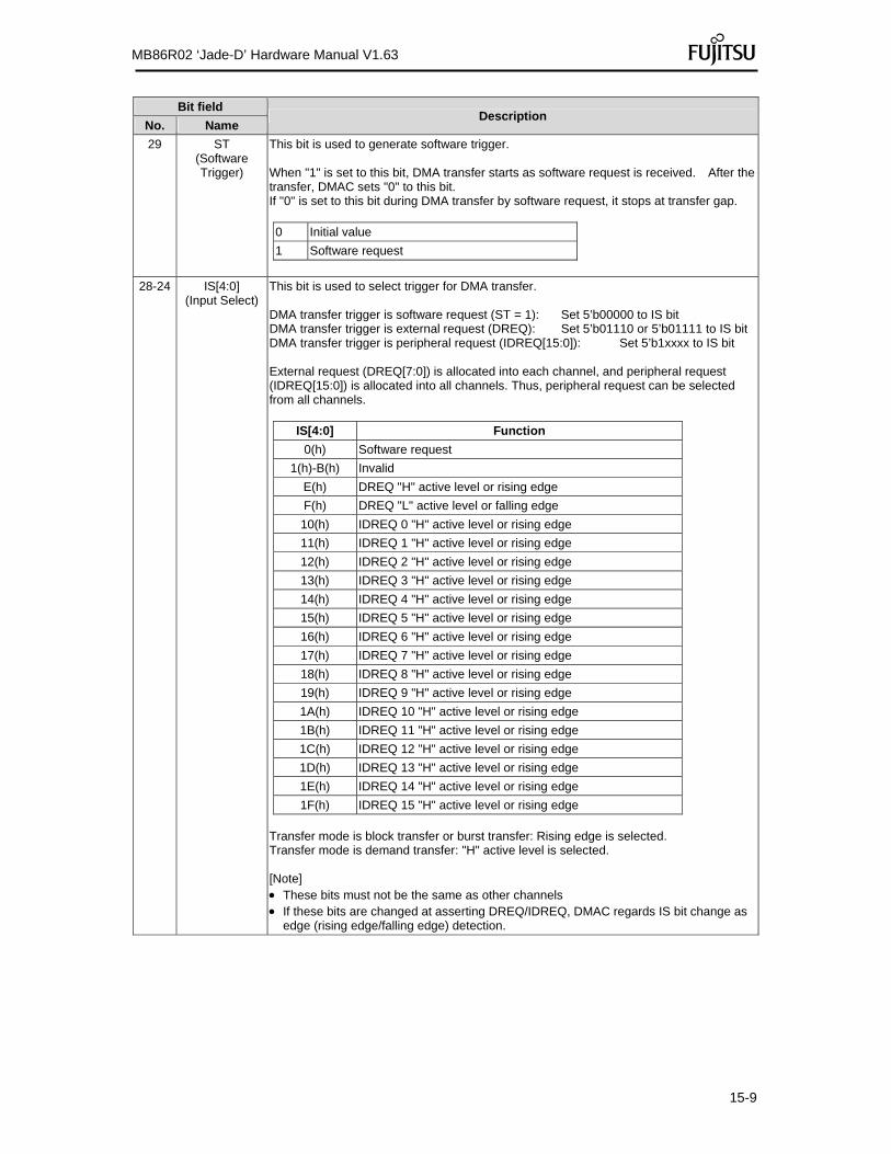
15-9
MB86R02 ‘Jade-D’ Hardware Manual V1.63
Bit field Description
No. Name
29 ST (Software Trigger)
This bit is used to generate software trigger. When "1" is set to this bit, DMA transfer starts as software request is received. After the transfer, DMAC sets "0" to this bit. If "0" is set to this bit during DMA transfer by software request, it stops at transfer gap. 0 Initial value
1 Software request
28-24 IS[4:0] (Input Select)
This bit is used to select trigger for DMA transfer. DMA transfer trigger is software request (ST = 1): Set 5’b00000 to IS bit DMA transfer trigger is external request (DREQ): Set 5’b01110 or 5’b01111 to IS bit DMA transfer trigger is peripheral request (IDREQ[15:0]): Set 5’b1xxxx to IS bit External request (DREQ[7:0]) is allocated into each channel, and peripheral request (IDREQ[15:0]) is allocated into all channels. Thus, peripheral request can be selected from all channels.
IS[4:0] Function
0(h) Software request
1(h)-B(h) Invalid
E(h) DREQ "H" active level or rising edge
F(h) DREQ "L" active level or falling edge
10(h) IDREQ 0 "H" active level or rising edge
11(h) IDREQ 1 "H" active level or rising edge
12(h) IDREQ 2 "H" active level or rising edge
13(h) IDREQ 3 "H" active level or rising edge
14(h) IDREQ 4 "H" active level or rising edge
15(h) IDREQ 5 "H" active level or rising edge
16(h) IDREQ 6 "H" active level or rising edge
17(h) IDREQ 7 "H" active level or rising edge
18(h) IDREQ 8 "H" active level or rising edge
19(h) IDREQ 9 "H" active level or rising edge
1A(h) IDREQ 10 "H" active level or rising edge
1B(h) IDREQ 11 "H" active level or rising edge
1C(h) IDREQ 12 "H" active level or rising edge
1D(h) IDREQ 13 "H" active level or rising edge
1E(h) IDREQ 14 "H" active level or rising edge
1F(h) IDREQ 15 "H" active level or rising edge Transfer mode is block transfer or burst transfer: Rising edge is selected. Transfer mode is demand transfer: "H" active level is selected. [Note] These bits must not be the same as other channels If these bits are changed at asserting DREQ/IDREQ, DMAC regards IS bit change as
edge (rising edge/falling edge) detection.

15-10
MB86R02 ‘Jade-D’ Hardware Manual V1.63
Bit field Description
No. Name
23-20 BT[3:0] (Beat Type)
These bits are used to select beat transfer on AHB. When these bits are set to Normal or Single, single source access and single destination access are alternately performed. If these bits are set to INCR* or WRAP*, contiguous source access and contiguous destination access are alternately performed. DMAC has 64 byte of FIFO that is shared in all channels. FIFO is used for INCR* and WRAP* DMA transfer. Refer to the AMBA specifications (v2.0) for INCR* and WRAP*. When INCR (undefined length burst) is set, the burst length is specified by the BC bit.
BT[3:0] Function
0(h) Normal (same as Single) (Initial value)
1(h)-7(h) Invalid
8(h) Single (same as Normal)
9(h) INCR
A(h) WRAP4
B(h) INCR4
C(h) WRAP8
D(h) INCR8
E(h) WRAP16
F(h) INCR16 While DMACB/MS are set to block transfer and burst transfer, fixed length burst (INCR*, WRAP*) and undefined length burst (INCR) are valid. When DMACB/MS are set to demand transfer, BT should be set to Normal or Single.
19-16 BC[3:0] (Block Count)
These bits are used to specify number of block for block/burst transfer. When transfer mode is demand transfer, be sure to set 4'b0000 to BC. Max. block quantity is 16. These bits are valid when beat transfer type is Normal, Single, or INCR. When other types of beat (fixed length burst and lap) are set, these bits are ignored. In addition, they are able to be read during DMA transfer. After single source access and single destination access are properly completed, normally BC bit is decremented for 1. [Note] These bits are settable even beat type bit (BT[3:0]) is INCR, however read data of BC after starting DMA transfer is always 4’h0 in INCR DMA transfer so that BC does not need to be monitored during the transfer. After DMA transfer is completed properly, DMAC sets 4’b0000 to these bits.
BC[3:0] Function
x(h) Number of blocks minus 1 (initial value: 4’b0000)
15-0 TC[15:0] (Transfer Count)
These bits are used to specify number of block/burst/demand transfer. Max. number of transfer is 65536. Any kind of bit type is valid for BT. These bits are readable during DMA transfer. After BC becomes "0" and DMA transfer is properly completed, normally TC bit is decremented for 1 in the Normal or Single mode (BT = Normal or Single.) In other beat transfer modes (INCR, INCR*, and WRAP*), TC bit is decremented for 1 after completing consecutive source/destination access operation (for example, when 4 consecutive source accesses and 4 consecutive destination accesses are completed, INCR4’s TC bit is decremented for 1.) After DMA transfer is completed properly, DMAC sets 16’h0000 to these bits.
TC[3:0] Function
x(h) Number of transfers minus 1 (initial value: 16’h0000)

15-11
MB86R02 ‘Jade-D’ Hardware Manual V1.63
15.6.4 DMA configuration B register (DMACBx)
Address
ch0:FFFD_0000+14 (h) ch1:FFFD_0000+24 (h) ch2:FFFD_0000+34 (h) ch3:FFFD_0000+44 (h)
ch4:FFFD_0000+54 (h) ch5:FFFD_0000+64 (h) ch6:FFFD_0000+74 (h) ch7:FFFD_0000+84 (h)
Bit 31 30 29 28 27 26 25 24 23 22 21 20 19 18 17 16 Name TT[1:0] MS[1:0] TW[1:0] FS FD RC RS RD EI CI SS[2:0] R/W R/W R/W R/W R/W R/W R/W R/W R/W R/W R/W R/W R/W R/W R/W0 R/W0 R/W0
Initial value 0 0 0 0 0 0 0 0 0 0 0 0 0 0 0 0 Bit 15 14 13 12 11 10 9 8 7 6 5 4 3 2 1 0
Name SP[3:0] DP[3:0] (Reserved) R/W R/W R/W R/W R/W R/W R/W R/W R/W R R R R R R R R
Initial value 0 0 0 0 0 0 0 0 0 0 0 0 0 0 0 0
Bit field
Description No. Name
31-30 TT[1:0] (Transfer Type)
These bits are used to specify transfer type. Currently, only 2 cycle transfer mode is available for DMAC.
TT[1:0] Function
0(h) 2 cycle transfer (initial value)
Other than 0(h)
Reserved
29-28 MS[1:0] (Mode Select)
These bits are used to select transfer mode.
MS[1:0] Function
0(h) Block transmission mode (initial value)
1(h) Burst transmission mode
2(h) Demand transmission mode
3(h) Reserved
27-26 TW[1:0] (Transfer
Width)
These bits are used to specify transfer data width. HSIZE of DMAC issues this value on AHB.
TW[1:0] Function
0(h) Byte (initial value)
1(h) Half-word
2(h) Word
3(h) Reserved
25 FS (Fixed Source)
This bit is used to fix source address. When the address needs to be added after each transfer, "0" must be set to this bit.
FS Function
0(h) Source address is incremented (initial value)
1(h) Source address is fixed
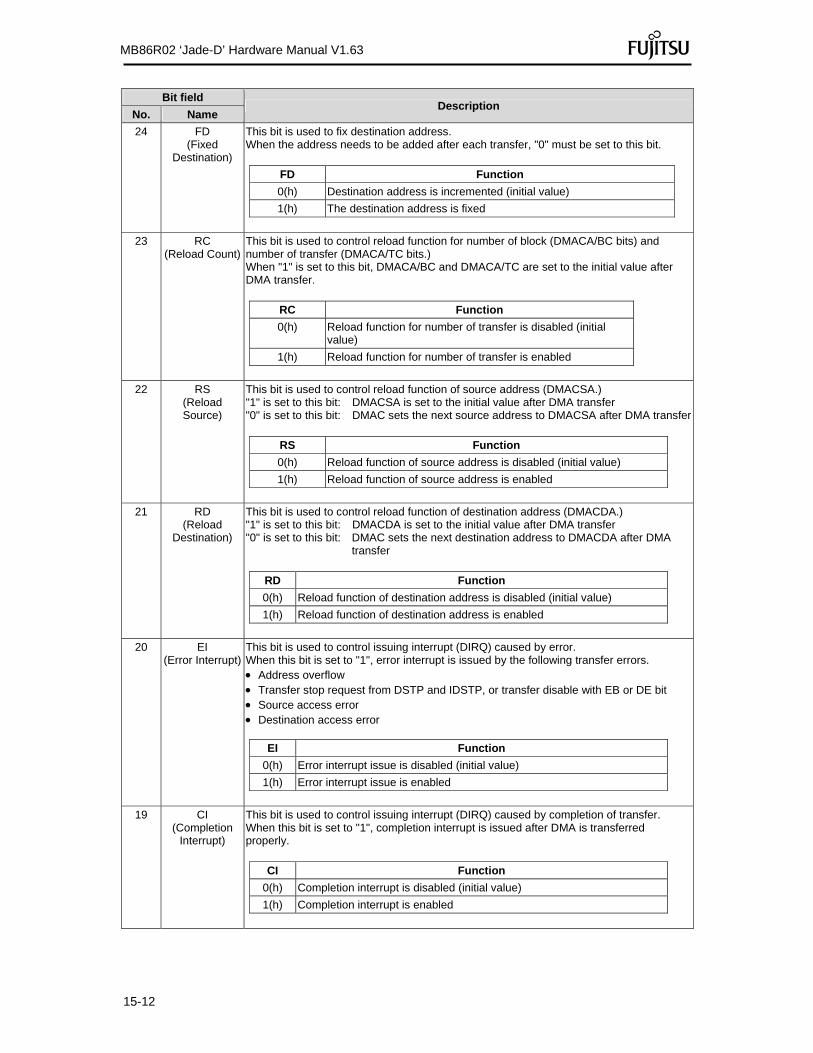
15-12
MB86R02 ‘Jade-D’ Hardware Manual V1.63
Bit field Description
No. Name
24 FD (Fixed
Destination)
This bit is used to fix destination address. When the address needs to be added after each transfer, "0" must be set to this bit.
FD Function
0(h) Destination address is incremented (initial value)
1(h) The destination address is fixed
23 RC (Reload Count)
This bit is used to control reload function for number of block (DMACA/BC bits) and number of transfer (DMACA/TC bits.) When "1" is set to this bit, DMACA/BC and DMACA/TC are set to the initial value after DMA transfer.
RC Function
0(h) Reload function for number of transfer is disabled (initial value)
1(h) Reload function for number of transfer is enabled
22 RS (Reload Source)
This bit is used to control reload function of source address (DMACSA.) "1" is set to this bit: DMACSA is set to the initial value after DMA transfer "0" is set to this bit: DMAC sets the next source address to DMACSA after DMA transfer
RS Function
0(h) Reload function of source address is disabled (initial value)
1(h) Reload function of source address is enabled
21 RD (Reload
Destination)
This bit is used to control reload function of destination address (DMACDA.) "1" is set to this bit: DMACDA is set to the initial value after DMA transfer "0" is set to this bit: DMAC sets the next destination address to DMACDA after DMA
transfer
RD Function
0(h) Reload function of destination address is disabled (initial value)
1(h) Reload function of destination address is enabled
20 EI (Error Interrupt)
This bit is used to control issuing interrupt (DIRQ) caused by error. When this bit is set to "1", error interrupt is issued by the following transfer errors. Address overflow
Transfer stop request from DSTP and IDSTP, or transfer disable with EB or DE bit Source access error Destination access error
EI Function
0(h) Error interrupt issue is disabled (initial value)
1(h) Error interrupt issue is enabled
19 CI (Completion
Interrupt)
This bit is used to control issuing interrupt (DIRQ) caused by completion of transfer. When this bit is set to "1", completion interrupt is issued after DMA is transferred properly.
CI Function
0(h) Completion interrupt is disabled (initial value)
1(h) Completion interrupt is enabled

15-13
MB86R02 ‘Jade-D’ Hardware Manual V1.63
Bit field Description
No. Name
18-16 SS[2:0] (Stop Status)
These bits are used to show end code of DMA transfer which is shown below. These bits are also used to release interrupt (DIRQ) which is performed by writing 3'b000 to these bits when interrupt becomes error or it is issued by normal termination.
SS Function Status type 0(h) Initial value None
1(h) Address overflow Error
2(h) Transfer stop request Error
3(h) Source access error Error
4(h) Destination access error Error
5(h) Normal termination End
6(h) Reserved
7(h) DMA discontinuance None When various errors occur at the same time, end code is displayed by the following priority. High priority Reset Clear by 3'b000 writing Address overflow Demand stop Source access error Destination access error Low priority
15-12 SP[3:0] (Source
Protection)
These bits are used to control source protection. HPROT at source access issues this value to AHB; however it is not performed if source target does not equip protection function.
SP Function
x(h) Protection code (initial value: 4'b0000.)
11-8 DP[3:0] (Destination Protection)
These bits are used to control destination protection. HPROT at destination access issues this value to AHB; however it is not performed if source target does not equip protection function.
DP Function
x(h) Protection code (initial value: 4'b0000.)
7-0 (Reserved) Reserved bits. Write access is ignored. Read value of this bit is always "0".

15-14
MB86R02 ‘Jade-D’ Hardware Manual V1.63
15.6.5 DMAC source address register (DMACSAx)
Address
ch0:FFFD_0000+18 (h) ch1:FFFD_0000+28 (h) ch2:FFFD_0000+38 (h) ch3:FFFD_0000+48 (h)
ch4:FFFD_0000+58 (h) ch5:FFFD_0000+68 (h) ch6:FFFD_0000+78 (h) ch7:FFFD_0000+88 (h)
Bit 31 30 29 28 27 26 25 24 23 22 21 20 19 18 17 16 Name DMACSA[31:16] R/W R/W R/W R/W R/W R/W R/W R/W R/W R/W R/W R/W R/W R/W R/W R/W R/W
Initial value 0 0 0 0 0 0 0 0 0 0 0 0 0 0 0 0 Bit 15 14 13 12 11 10 9 8 7 6 5 4 3 2 1 0
Name DMACSA[15:0] R/W R/W R/W R/W R/W R/W R/W R/W R/W R/W R/W R/W R/W R/W R/W R/W R/W
Initial value 0 0 0 0 0 0 0 0 0 0 0 0 0 0 0 0
Bit field
Description No. Name
31-0 DMACSA[31:0] (DMAC Source
Address)
These bits are used to specify source address to start DMA transfer, and they are able to be read during DMA transfer. When fixed address function (DMACB/FS) is disabled, these bits are incremented according to the transfer width (DMACB/TB) after completing source address properly. After the DMA transfer, DMAC sets the next source address to these bits. [Note] It is prohibited to set DMAC register address to DMACSA.
DMACSA Function
x(h) Source address to start DMA transfer (Initial value: 32'h00000000)

15-15
MB86R02 ‘Jade-D’ Hardware Manual V1.63
15.6.6 DMAC destination address register (DMACDAx)
Address
ch0:FFFD0000+1C (h) ch1:FFFD0000+2C (h) ch2:FFFD0000+3C (h) ch3:FFFD0000+4C (h)
ch4:FFFD0000+5C (h) ch5:FFFD0000+6C (h) ch6:FFFD0000+7C (h) ch7:FFFD0000+8C (h)
Bit 31 30 29 28 27 26 25 24 23 22 21 20 19 18 17 16 Name DMACDA[31:16] R/W R/W R/W R/W R/W R/W R/W R/W R/W R/W R/W R/W R/W R/W R/W R/W R/W
Initial value 0 0 0 0 0 0 0 0 0 0 0 0 0 0 0 0 Bit 15 14 13 12 11 10 9 8 7 6 5 4 3 2 1 0
Name DMACDA[15:0] R/W R/W R/W R/W R/W R/W R/W R/W R/W R/W R/W R/W R/W R/W R/W R/W R/W
Initial value 0 0 0 0 0 0 0 0 0 0 0 0 0 0 0 0
Bit field
Description No. Name
31-0 DMACDA[31:0] (DMAC
Destination Address)
These bits are used to specify destination address to start DMA transfer, and they are able to be read during DMA transfer. When fixed address function (DMACB/FD) is disabled, these bits are incremented according to the transfer width (DMACB/TB) after completing destination address properly. After DMA transfer, DMAC sets the next destination address to these bits. [Note] It is prohibited to set DMAC register address to DMACDA.
DMACDA Function
x(h) Destination address to start DMA transfer (Initial value: 32'h00000000)

15-16
MB86R02 ‘Jade-D’ Hardware Manual V1.63
15.7 Operation
This section describes the operation of the DMAC.
15.7.1 Transfer modes
The DMAC has 3 transfer modes which are set using DMACB.MS[1:0].
15.7.1.1 Block transfer
Operation In block transfer mode, DMA transfer is specified by the number of blocks (DMACA/BC) to be executed by 1 transfer request. When the number of transfer (DMACA/TC) is set to a value other than "0", TC is decremented by 1 after completing the DMA transfer of BC. After the last transfer (BC is 4'h0 and TC is 16'h0000), DMA transfer is completed.
Transfer gap After completing BC transfer, DMAC temporarily negates the bus request to the arbiter in block transfer mode. This operation prevents the DMAC from blocking the bus. This transfer gap can be used to update the register settings (e.g. disable/interruption setting) to the DMAC during DMA transfer.
Transfer request Three types of request are valid in this mode: request by software, external request (DREQ) and peripheral request (IDREQ).. Software request
Set "1" to DMACA/ST and set 5'b00000 to DMACA/IS External request
Set "0" to DMACA/ST, and set 5'b01110 (rising edge of transfer request) or 5'b01111 (falling edge of transfer request) to DMACA/IS
Peripheral request Set "0" to DMACA/ST, and set 5'b1**** (rising edge of transfer request) to DMACA/IS
When a external request or peripheral request is selected, the DMAC detects the transfer request edge. When BC's DMA transfer is executed by either of those requests, the DMAC is unable to detect the next transfer; however it is able to detect the next transfer request after BC's DMA transfer has been completed.

15-17
MB86R02 ‘Jade-D’ Hardware Manual V1.63
Restrictions When DMA transfer is performed by an external (DREQ) or peripheral (IDREQ) request, there are restrictions for external and peripheral signal pins.
1. DREQ/IDREQ
DREQ/IDREQ must be asserted for at least 2 cycles of the AHB clock (HCLK). There is no restriction for the timing of negating DREQ/IDREQ. After asserting DACK/IDACK, DMAC is able to accept new a transfer request (edge of DREQ/IDREQ) for the next DMA transfer.
2. DACK/IDACK
After the DMAC transfers data to the destination address, DACK/IDACK are asserted for 1 cycle of the AHB clock (HCLK). If access to the destination is executed correctly, this signal is asserted. If destination issues, error, retry or split responses occur on the AHB, it is not asserted. In block transfer mode, these signals indicate that the DMAC has correctly performed destination access.
3. DEOP/IDEOP
Basically, DEOP/IDEOP is asserted for 1 AHB clock (HCLK) cycle if the DMAC terminates DMA transfer properly or abnormally. Abnormal DMA transfer includes the following cases: Forced termination by DSTP/IDSTP Forced termination by setting 1'b0 to DMACA/EB Reception of an error response from the source/destination
4. DSTP/IDSTP
DSTP/IDSTP are used to forcibly terminate DMA transfer and asserting them during the transfer is permitted (it is also permissible to assert DSTP/IDSTP while DMA data is not transferred due to a transfer gap or an interrupt function). If these signals are used to forcibly terminate DMA transfer, they are not asserted until DEOP/IDEOP are asserted.
5. Exceptional operation of DEOP/IDEOP If DSTP/IDSTP are asserted immediately after asserting DREQ/DSTP, the DMAC may request the bus to execute an IDLE transfer. In this case, the DMAC may assert DEOP/IDEOP for 2 or more cycles of the AHB clock (HCLK). The assertion period of DEOP/IDEOP depends on the number of previous master transfer cycles. Figure 15-2 shows an example of this exception operation.

15-18
MB86R02 ‘Jade-D’ Hardware Manual V1.63
DACK
DREQ
DEOP
DSTP
HCLK
HBUSREQM (HDMAC)
HGRANTM (HDMAC)
HMASTER
Control
HREADY
IDLE
HRESP
HDMAC
OK
Other master
NONSEQ or SEQ READ or WRITE
Other master
NONSEQ or SEQ READ or WRITE
Figure 15-2 Example of DEOP/IDEOP exception operation
DREQ/IDREQ, DACK/IDACK, DEOP/IDEOP, and DSTP/IDSTP are not valid when DMA transfer is performed in software request mode.
Timing chart Figure 15-3 shows a block transfer as a timing chart.

15-19
MB86R02 ‘Jade-D’ Hardware Manual V1.63
DREQ
DACK
DEOP
DSTP
HCLK
HADDR
HWRITE
Control
External trigger
Software trigger
DMACA[31:24]
HWDATA
HRDATA
HBUSREQ
HGRANT
HREADY
HRESP
HMASTER CPU HDMAC CPU HDMAC CPU
OK
SA DA SA DA SA DA SA DA
HTRANS N N N N N N N N I I
Data Data Data
Data Data Data Data
0x00 0xA0
DMACA[19:16] 0x0 0x1 BC
0x00
0x0 0x1 0x0
DMACA[15:0] 0x0 0x1 TC
0x0
DMACSA
DMACDA
SA0 SA1 SA2 SA3 SA4
DA0 DA1 DA2 DA3 DA4
Break of transfer
Data
Figure 15-3 Block transfer (for BC = 0x1 and TC = 0x1)

15-20
MB86R02 ‘Jade-D’ Hardware Manual V1.63
15.7.1.2 Limitations with I2S DMA
The I2S unit is only able to handle a subset of the DMA transfer modes that the DMA Controller supports. For this reason, please take note of the following: Threshold values in the I2SxINTCNT register (I2S, offset 0x20) must match the BC values of
the respective DMAC register DMACAx (DMACA0 ... DMACA7, various offsets)
Each block matches one transfer request
The selected DMAC transfer mode must be 'Block Transfer' (check the DMACBx registers)
Demand and burst transfer modes can not be used with I2S
In order for DMA transfers to work with the I2S unit, each transfer has to transmit/receive as many words to/from FIFO as there are valid entries. When DMA has finished, the same setup for the next transfer has to be configured again in the DMAC and in the I2S module.

15-21
MB86R02 ‘Jade-D’ Hardware Manual V1.63
15.7.1.3 Burst transfer
Operation In burst transfer mode, DMA transfer is executed for a number of blocks, multiplied by the number of transfers (DMACA/BC DMACA/TC) using 1 request. When the number of transfers (DMACA/TC) is set to values other than "0", TC is decremented by 1 after completing the DMA transfer. DMA transfer is completed after the last transfer (BC is 4'h0 and TC is 16'h0000).
Transfer gap After completing DMA transfer, DMAC negates the bus request to the arbiter so that a transfer gap does not occur in burst transfer mode. Register setting changes during DMA transfer (e.g. disable/interruption setting) are reflected after completing DMA transfer.
Transfer request Software request, external (DREQ), and peripheral (IDREQ) requests are valid in this mode. Software request
Set "1" to DMACA/ST and set 5'b00000 to DMACA/IS External request
Set "0" to DMACA/ST and set 5'b01110 (rising edge of transfer request) or 5'b01111 (falling edge of transfer request) to DMACA/IS
Peripheral request Set "0" to DMACA/ST and set 5'b1**** (rising edge of transfer request) to DMACA/IS
When external request or peripheral request mode is selected, the DMAC detects the transfer request edge. When DMA transfer of BC TC is executed by either of these requests, the DMAC is unable to detect the next transfer; however it is able to detect the next transfer request after DMA transfer of BC TC has been completed.

15-22
MB86R02 ‘Jade-D’ Hardware Manual V1.63
Restrictions When DMA transfer is performed by external (DREQ) and peripheral (IDREQ) requests, there are some restrictions for external and peripheral signal pins.
1. DREQ/IDREQ DREQ/IDREQ must be asserted for at least 2 cycles of the AHB clock (HCLK). There is no restriction for the timing of the negation of DREQ/IDREQ. After completing DMA transfer in BC TC and asserting DACK/IDACK and DEOP/IDEOP, a new transfer request (edge of DREQ/IDREQ) can be accepted for the next DMA transfer.
2. DACK/IDACK
After the DMAC has transferred data to the destination address, DACK/IDACK are asserted for 1 cycle of the AHB clock (HCLK). If access to the destination was done correctly, this signal is asserted. If the destination issues error, retry, or split responses on the AHB bus, this signal is not asserted. In burst transfer mode, these signals indicate that the DMAC has performed destination access properly.
3. DEOP/IDEOP Basically, DEOP/IDEOP are asserted for 1 AHB clock (HCLK) cycle when the DMAC ends DMA transfer properly or abnormally. Abnormal DMA transfer includes the following cases: Forced termination by DSTP/IDSTP Forced termination by setting 1'b0 to DMACA/EB Reception of an error response from the source/destination
4. DSTP/IDSTP
DSTP/IDSTP are used to forcibly terminate DMA transfer and it is permissible to assert them during transfer (it is also permissible to assert DSTP/IDSTP while DMA is not transferring due to the transfer gap or an interrupt function). If these signals are used to forcibly terminate DMA transfer, they are not asserted until DEOP/IDEOP are asserted.
5. Exceptional operation of DEOP/IDEOP If DSTP/IDSTP are asserted immediately after DREQ/DSTP have been asserted, the DMAC may request the bus to execute an IDLE transfer. In this case, the DMAC may assert DEOP/IDEOP for 2 cycles or more of the AHB clock (HCLK). The assertion period of DEOP/IDEOP depends on the number of previous master transfer cycles. Figure 15-4 shows an example of this exception operation.

15-23
MB86R02 ‘Jade-D’ Hardware Manual V1.63
DACK
DREQ
DEOP
DSTP
HCLK
HBUSREQM (HDMAC)
HGRANTM (HDMAC)
HMASTER
Control
HREADY
IDLE READ
HRESP
NOSEQ or SEQ READ or WRITE
HDMAC
OK
Other master Other master
NOSEQ or SEQ READ or WRITE
Figure 15-4 Example of DEOP/IDEOP exception operation DREQ/IDREQ, DACK/IDACK, DEOP/IDEOP, and DSTP/IDSTP are not valid if DMA transfer is performed by software reset.
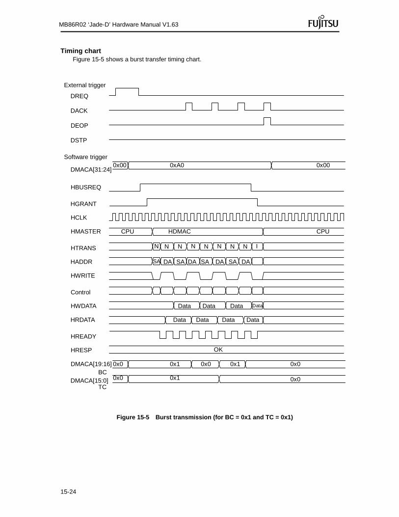
15-24
MB86R02 ‘Jade-D’ Hardware Manual V1.63
Timing chart Figure 15-5 shows a burst transfer timing chart.
DREQ
DACK
DEOP
DSTP
HCLK
HADDR
HWRITE
Control
External trigger
Software trigger
DMACA[31:24]
HWDATA
HRDATA
HBUSREQ
HGRANT
HREADY
HRESP
HMASTER CPU HDMAC CPU
OK
SA DA SA DA SA DA
HTRANS N N N N N I N
Data Data Data
Data Data Data
0x00 0xA0
DMACA[19:16] 0x0 0x1 BC
0x00
0x0 0x1 0x0
DMACA[15:0] 0x0 0x1
TC 0x0
SA DA
N N
Data
Data
Figure 15-5 Burst transmission (for BC = 0x1 and TC = 0x1)

15-25
MB86R02 ‘Jade-D’ Hardware Manual V1.63
15.7.1.4 Demand transfer
Operation In demand transfer mode, DMA transfer is executed as a one-off transfer when the transfer request is asserted and the number of transfers is set in the DMACA/TC registers. In this case, DMACA/BC is set to "0". In this mode, DMACA/BC values are ignored. DMACA/TC are decremented by 1 after the DMA transfer has completed. DMA transfer therefore ends after the last transfer (TC is16’h0000) has been completed.
Transfer gap After completing 1 transfer, DMAC temporarily negates the bus request to the arbiter even though the transfer request is asserted. This operation prevents the DMAC from blocking the bus. This transfer gap can be used to update register settings (e.g. disable/interruption setting) to the DMAC during DMA transfers.
Transfer request External (DREQ) and peripheral (IDREQ) requests are permissible in demand transfer mode, however software requests are prohibited. External request
Set "0" to DMACA/ST, and set 5'b01110 (H level of transfer request) or 5'b01111 (L level of transfer request) to DMACA/IS
Peripheral request Set "0" to DMACA/ST, and set 5'b1**** (H level of transfer request) to DMACA/IS
When an external request or peripheral request is selected, the DMAC detects the transfer request level.

15-26
MB86R02 ‘Jade-D’ Hardware Manual V1.63
Restrictions When DMA transfer is performed by external (DREQ) or peripheral (IDREQ) requests, there are some restrictions for the external and peripheral signal pins.
6. DREQ/IDREQ
DREQ/IDREQ must remain asserted until DACK/IDACK are asserted. After they have been asserted, DREQ/IDREQ must be negated within AHB clock (HCLK) cycles of "source access cycle + destination access cycle – 1". If the negation timing of DREQ/IDREQ violates the restrictions, the DMAC could start the next transfer operation. After completing 1 DMATE transfer and DACK/IDACK are asserted, the DMAC is able to receive new transfer requests (DREQ/IDREQ level) for the next DMA transfers after the negating period described above.
7. DACK/IDACK
After the DMAC has transferred the control signal to the source address, DACK/IDACK are asserted for 1 cycle of the AHB clock (HCLK). In demand transfer mode, these signals indicate that the DMAC is receiving a demand transfer request.
8. DEOP/IDEOP Basically, DEOP/IDEOP are asserted for 1 AHB clock (HCLK) cycle when DMAC ends DMA transfer properly or abnormally. Abnormal DMA transfer includes following cases: Forced termination by DSTP/IDSTP Forced termination by setting 1'b0 to DMACA/EB Receiving error response from source/destination
DSTP/IDSTP are used to forcibly terminate DMA transfer. Asserting them during DMA transfer is permissible (it is also permissible to assert DSTP/IDSTP while DMA is not transferring due to a transfer gap or interrupt function). If these signals are used to forcibly terminate DMA transfer, they are not asserted until DEOP/IDEOP have been asserted.
9. DEOP/IDEOP exception operation If DSTP/IDSTP are asserted immediately after DREQ/DSTP have been asserted, the DMAC may request the bus to execute an IDLE transfer. In this case, the DMAC may assert DEOP/IDEOP for 2 or more AHB clock (HCLK) cycles. The DEOP/IDEOP assertion period depends on the number of previous master transfer cycles. Figure 15-6 shows example of this exception operation.

15-27
MB86R02 ‘Jade-D’ Hardware Manual V1.63
DACK
DREQ
DEOP
DSTP
HCLK
HBUSREQM (HDMAC)
HGRANTM (HDMAC)
HMASTER
Control
HREADY
IDLE READ
HRESP
NOSEQ or SEQ READ or WRITE
HDMAC
OK
Other mster Other mster
NOSEQ or SEQ READ or WRITE
Figure 15-6 Example of DEOP/IDEOP exception operation
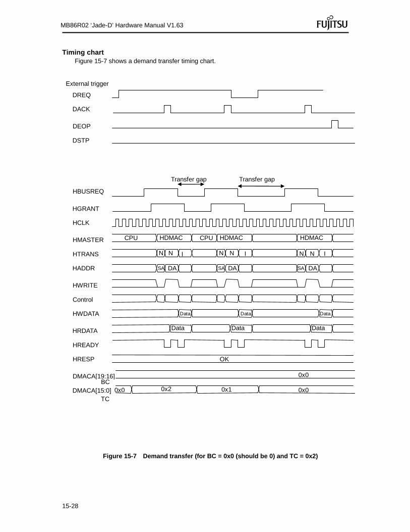
15-28
MB86R02 ‘Jade-D’ Hardware Manual V1.63
Timing chart Figure 15-7 shows a demand transfer timing chart.
DREQ
DACK
DEOP
DSTP
HCLK
HADDR
HWRITE
Control
External trigger
HWDATA
HRDATA
HBUSREQ
HGRANT
HREADY
HRESP
HMASTER CPU HDMAC CPU
OK
SA DA
HTRANS N N I
Data
Data
DMACA[19:16]
0x2BC
0x1 0x0 DMACA[15:0] 0x0
TC
0x0
HDMAC
SA DA
N N I
HDMAC
SA DA
N N I
Data
Data
Data
Data
Transfer gap Transfer gap
Figure 15-7 Demand transfer (for BC = 0x0 (should be 0) and TC = 0x2)
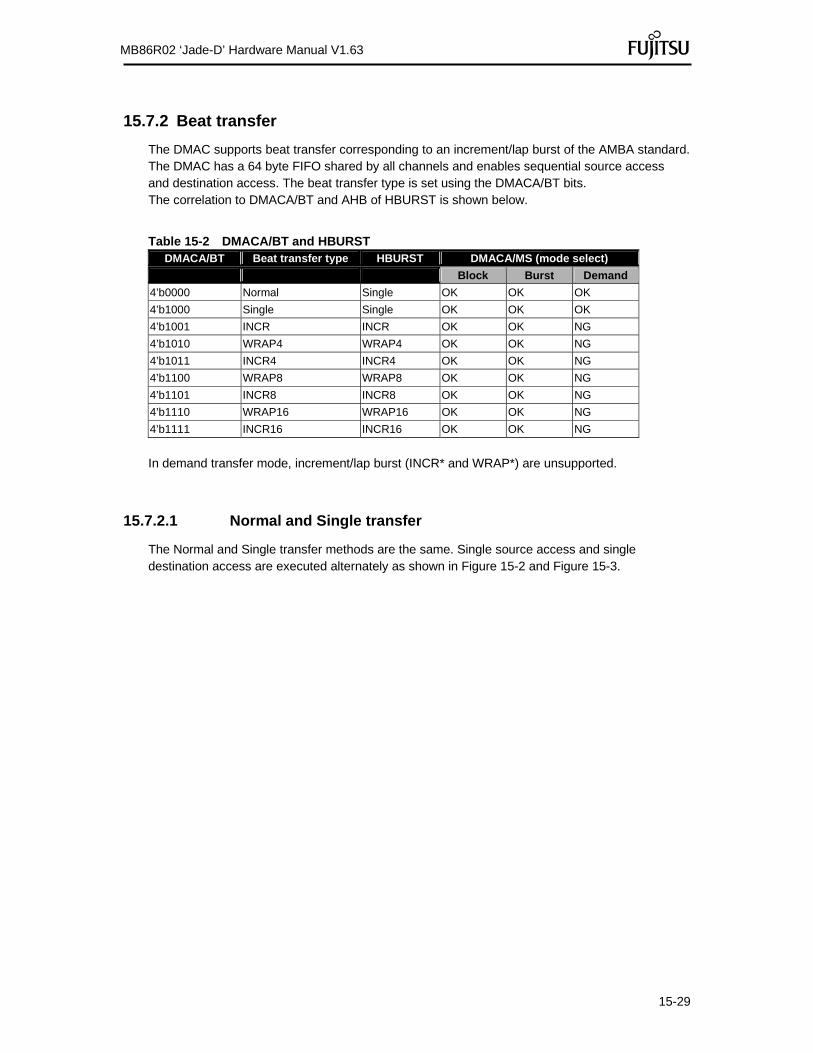
15-29
MB86R02 ‘Jade-D’ Hardware Manual V1.63
15.7.2 Beat transfer
The DMAC supports beat transfer corresponding to an increment/lap burst of the AMBA standard. The DMAC has a 64 byte FIFO shared by all channels and enables sequential source access and destination access. The beat transfer type is set using the DMACA/BT bits. The correlation to DMACA/BT and AHB of HBURST is shown below.
Table 15-2 DMACA/BT and HBURST DMACA/BT Beat transfer type HBURST DMACA/MS (mode select)
Block Burst Demand
4’b0000 Normal Single OK OK OK
4’b1000 Single Single OK OK OK
4’b1001 INCR INCR OK OK NG
4’b1010 WRAP4 WRAP4 OK OK NG
4’b1011 INCR4 INCR4 OK OK NG
4’b1100 WRAP8 WRAP8 OK OK NG
4’b1101 INCR8 INCR8 OK OK NG
4’b1110 WRAP16 WRAP16 OK OK NG
4’b1111 INCR16 INCR16 OK OK NG
In demand transfer mode, increment/lap burst (INCR* and WRAP*) are unsupported.
15.7.2.1 Normal and Single transfer
The Normal and Single transfer methods are the same. Single source access and single destination access are executed alternately as shown in Figure 15-2 and Figure 15-3.

15-30
MB86R02 ‘Jade-D’ Hardware Manual V1.63
15.7.2.2 Increment and lap transfer
When increment beat transfer (INCR, INCR4, INCR8 and INCR16) or lap beat transfer (WRAP4, WRAP8, and WRAP16) are set to DMACA/BT, sequential source access and destination access are executed using the DMAC's 64 byte FIFO. In the case of INCR4 (DMACA/BT = 4'b1011), the DMAC performs 4 sequential source accesses. Output data from the source is stored in the DMAC's FIFO, then the data is sequentially driven to the destination.
HCLK
HADDR
HWRITE
Control
HWDATA
HRDATA
HBUSREQ
HGRANT
HREADY
HRESP
HMASTER CPU HDMAC CPU
OK
SA SA SA SA DA DA
HTRANS N S S S S IN
D4D1
D1
DMACA[19:16] BC
0x0
DMACA[15:0] TC
DA DA
S S
INCR4 INCR4
D2 D3
D2 D3
D4
0x0
Figure 15-8 Increment/Lap beat transfer (example of INCR4 block transfer)

15-31
MB86R02 ‘Jade-D’ Hardware Manual V1.63
15.7.3 Channel priority control
The DMAC controls the priority of each channel using the DMACR/PR bits.
15.7.3.1 Fixed priority
When this priority is set in the DMACR/PR bits, the priority order is fixed and bus usage is granted to the lowest numbered channel. The priority controller of the DMAC switches the channel when the active channel enters the transfer gap. In this way, if all the channels are active at the same time, the lowest numbered channel (ch0) can be selected by the priority controller to start a transfer. For example, the active channel (ch0) temporarily loses the bus during the transfer gap. The second lowest numbered channel (ch1) is then granted bus access. When ch1 loses the bus control during the transfer gap, it is given to ch0 again. As a result, these 2 channels are able to preferentially acquire bus usage in fixed priority mode. Figure 15-9 shows the defined channel ordering in fixed priority mode.
HBUSREQM
HGRANTM
HBUSREQM0 HBUSREQM1 HBUSREQM2 HBUSREQM3 HBUSREQM4 HBUSREQM5 HBUSREQM6 HBUSREQM7
Defined channel #0 #1 #0 #1 #0 #1 #0 #1 #2 #3 #2 #3 #2 #3 #2
HDMAC Internal
AHB
Figure 15-9 Defined channel ordering in fixed priority mode

15-32
MB86R02 ‘Jade-D’ Hardware Manual V1.63
15.7.3.2 Rotate priority
When rotation priority is set in the DMACR/PR bits, the priority order is rotated. After the bus is granted to the lowest numbered channel, the priority controller of DMAC switches the channel during the transfer gap of the active channel. In this way, if all the channels become active at the same time, the lowest numbered channel (ch0) is selected by the priority controller to enable transfer operation. In rotate priority mode, all channels are able to acquire the bus in turn. For example, the active channel (ch0) temporarily loses the bus during the transfer gap. Access is then granted to the second lowest numbered channel (ch1). When ch1 loses the bus access during the transfer gap, it is granted to the third lowest numbered channel (ch2.) Figure 15-10 shows the defined channel ordering in rotate priority mode.
HBUSREQM
HGRANTM
HBUSREQM0 HBUSREQM1 HBUSREQM2 HBUSREQM3 HBUSREQM4 HBUSREQM5 HBUSREQM6 HBUSREQM7
Defined channel #0 #1 #2 #3 #4 #5 #6 #7 #0 #1 #2 #3 #4 #5 #6
HDMAC Internal
AHB
Figure 15-10 Defined channel ordering in rotate priority mode

15-33
MB86R02 ‘Jade-D’ Hardware Manual V1.63
15.7.4 Retry, split, and error
The DMAC module supports retry and split responses from AHB slaves.
15.7.4.1 Retry and split
When the DMAC receives a retry or split response from an AHB slave during DMA transfer, it negates bus temporarily to reconstruct the contents to be retransmitted. Figure 15-11 shows an example of receiving a retry response during INCR4 DMA transfer.
HCLK
HADDR
HWRITE
Control
HWDATA
HRDATA
HBUSREQ
HGRANT
HREADY
HRESP
HMASTER CPU HDMAC CPU
OK
SA SA SA SA DA DA
HTRANS N S S S S IN
D4D1
D1
DMACA[19:16] BC
0x0
DMACA[15:0] TC
DA DA
S S
INCR4 INCR4
D2 D3
D2 D3
D4
0x0
RETRY OK
HDMAC
DA
N I
D4
INCR
Figure 15-11 Increment/Lap beat transfer (example of INCR4 block transfer) When DMAC negates bus temporarily, the channel received retry/split responses is continuously selected by DMAC's priority controller that transfer operation is able to start even though higher priority channel requests the bus

15-34
MB86R02 ‘Jade-D’ Hardware Manual V1.63
15.7.4.2 Error
When the DMAC receives an error reply from an AHB slave during DMA transfer, it negates the bus request and immediately stops the transfer even though it has not been completed. In this case, neither the Block/Transfer count register nor the Source/Destination address registers are updated.

15-35
MB86R02 ‘Jade-D’ Hardware Manual V1.63
15.8 DMAC Configuration Examples
15.8.1 DMA start in Single channel
Example of block and burst transfer by software request (with DMAC ch0)
ー
(2) Set DMAC source address register DMACSA0 ← 0x0000_0000
(1) Set DMA configuration register DMACR ← 0x80 (byte writing)
Source address is set.
DMA transfer is enabled.
(3) Set DMAC destination address register DMACDA0 ← 0x0100_0000
(4) Set DMA configuration B register
DMACB0 ← 0x0808_0000
Destination address is set.
Transfer mode, transfer data width, and completion interrupt are set. In this example, block transfer mode (MS[1:0] = 0H) is set as transfer mode. Burst transfer mode is able to be set by MS[1:0] = 1H.
DMA channel transfer control, software trigger, and number of block and transfer are set.
(5) Set DMA configuration A register DMACA0 ← 0xA00F_000F
Start DMA transfer
Remark: Setting order of step 1 ~ 4 is arbitrary; however, the one of step 5 is unable to be changed.
Note: DMA configuration register (DMACR) should be set using byte writes. For block and burst transfer by software request, the DMAC configuration A register
(DMACA) should be set last.

15-36
MB86R02 ‘Jade-D’ Hardware Manual V1.63
Example of demand transfer by software request (with DMAC ch0)
ー
(2) Set DMAC source address register DMACSA0 ← 0x0100_8000
(1) Set DMA configuration register DMACR ← 0x80 (byte writing)
Source address is set.
DMA transfer is enabled.
(3) Set DMAC destination address register DMACDA0 ← 0xFFFE_1000
(4) Set DMA configuration B register
DMACB0 ← 0x2108_0000
Destination address is set.
Transfer mode, transfer data width, and completion interrupt is set.
DMA channel transfer control, software trigger, and number of block and transfer are set.
(5) Set DMA configuration A register DMACA0 ← 0x9000_000A
Start DMA transfer
Remark: Setting order of step 1 ~ 5 is arbitrary; however, the last setting should be step 1 or 5.
Note: DMA configuration register (DMACR) should be set by byte writes.
15.8.2 DMA start in all channels (in demand transfer mode)
All channels are able to start simultaneously by setting the DMACR register after setting all DMA channel registers in demand transfer mode. In this case, the DMAC priority controller receives a request from all channels at the same time, and then transfer starts by selecting the channel according to the DMA channel priority, which is configurable using the PR bit of the DMACR.
16-1
MB86R02 ‘Jade-D’ Hardware Manual V1.63
16 Host Interface This chapter describes the Host Interface of the MB86R02.
16.1. Outline
The Host Interface module is an internal module connected to the AHB which is used for communication to an external host CPU (which is connected via the SPI interface). The host CPU can read and write to the internal module. From a host CPU point of view, this module functions as a slave, whereas it functions as a master internally.
16.2. Features
The Host Interface has the features described in the following sections.
16.2.1. Features
Accesses by the host CPU to the internal module can made using varying address bytes lengths within a range of 1 to 4 bytes. Additionally, the data byte length can be arbitrarily set within a range of 1 to 16 bytes. This means that the received number of bytes can be optimized and that forwarding can be done efficiently. These settings can be specified by the CMD byte, allowing a highly flexible solution that abstracts the type of host CPU in use and the access objects. Supports communication to a host CPU with an SPI interface The length of the SPI interface packets is variable to permit the use of variable length
addresses and data accesses Supports writes/reads to the internal module connected to the AHB (variable, from 1 to 16
bytes) Conforms to Freescale Semiconductor's advocacy SPI (CPOL=0, CPHA=0) Corresponds to the speed of general purpose CPUs (set the frequency of SPICLK to 1/2 or
less of the HCLK frequency) Host CPU handshaking communication makes software flow control possible
16.2.2. Limitations
The MB86R02 can only operate in slave mode whereas the host CPU is the bus master The packet sizes must be in 8 bit units No CRC error detection functionality. No automatic procedure for resends in the case of errors (no ARQ functionality) Supported burst transfer modes for the AHB are single, incr or incr4
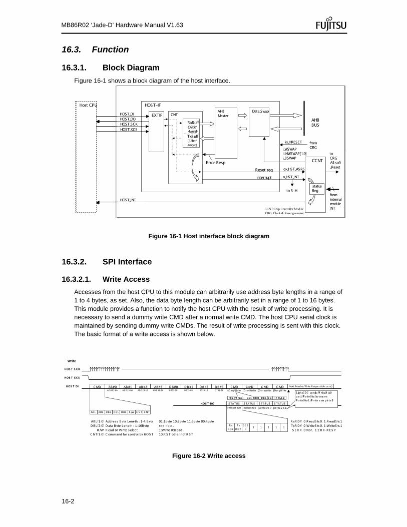
16-2
MB86R02 ‘Jade-D’ Hardware Manual V1.63
16.3. Function
16.3.1. Block Diagram
Figure 16-1 shows a block diagram of the host interface.
CCNT :Chip Controller ModuleCRG: Clock & Reset generator
o_HST_INT
HOST_DIHOST_DOHOST_SCKHOST_XCS
AHBBUS
Host CPU
INT
HOST-IF
EXTIF
Reset req
CNT
Error Resp
RxBuff(32bit*4word)TxBuff(32bit*4word)
Data_Swap
HOST_INT
AHBMaster
frominternalmoduleINT
interrupt
ox_HST_ASRST
toCRGAll_soft_Reset
CCNT:Chip Controller ModuleCRG: Clock & Reset generator
i_WSWAPi_HWSWAP[1:0]i_BSWAP CCNT
statusReg
fromCRG
ix_HRESET
to R-H
Figure 16-1 Host interface block diagram
16.3.2. SPI Interface
16.3.2.1. Write Access
Accesses from the host CPU to this module can arbitrarily use address byte lengths in a range of 1 to 4 bytes, as set. Also, the data byte length can be arbitrarily set in a range of 1 to 16 bytes. This module provides a function to notify the host CPU with the result of write processing. It is necessary to send a dummy write CMD after a normal write CMD. The host CPU serial clock is maintained by sending dummy write CMDs. The result of write processing is sent with this clock. The basic format of a write access is shown below.
TxR DYR xR DY
S E R R
(DmyWrite
(WriteS ts 0 (WriteS ts 1(WriteS ts 0 (WriteS ts 0
HOS T DO
ADD07‐00 ADD15‐08 ADD 23‐16 ADD31‐24 DT07‐00 D T15‐08 DT23‐16 DT31‐24
C MD AB#0 AB#1 AB#2 AB#3 DB#0 DB#1 DB#2 DB#3
HOS T S CK
HOS T XCS
HOS T DI
ABL[1:0] Address Byte Length : 1‐4 ByteDBL[2:0] Data Byte Length : 1‐16Byte
R /W R ead or Write s elect
Write
ABL ABL DBL DBL DBL R /W C NT C NT
01:1byte 10:2byte 11:3byte 00:4byte
1:Write 0:R ead
CMD Next Read or Write Reques t (Acces s )
S TATUS S TATUS S TATUS S TATUS
R x
R DY
Tx
R DY1
S E R
R1 1 1 1
(DmyWriteCMD
(DmyWriteC MD
(DmyWriteC MD
0:WriteS ts 0, 1:WriteS ts 10:R eadS ts 0, 1:R eadS ts 1
0:Nor, 1:E R R ‐R E S PC NT[1:0] C ommand for control by HOS T 10:R S T other:not R S T
Figure 16-2 Write access
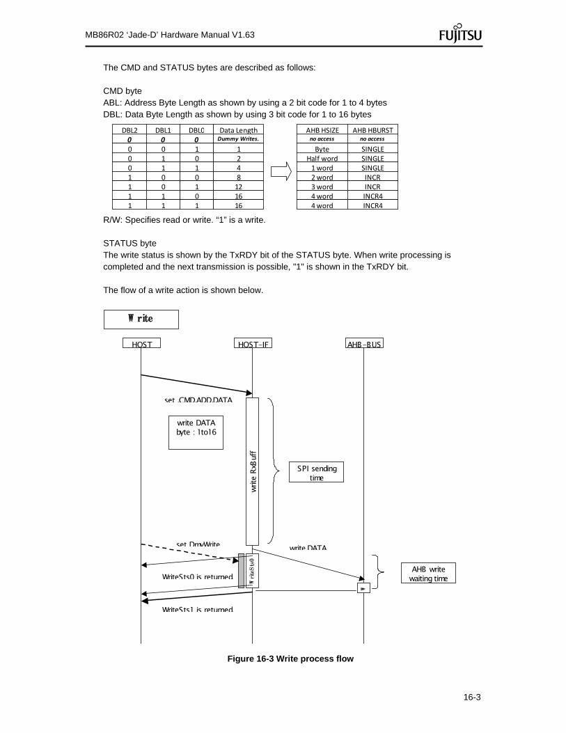
16-3
MB86R02 ‘Jade-D’ Hardware Manual V1.63
The CMD and STATUS bytes are described as follows: CMD byte ABL: Address Byte Length as shown by using a 2 bit code for 1 to 4 bytes DBL: Data Byte Length as shown by using 3 bit code for 1 to 16 bytes
DBL2 DBL1 DBL0 Data Length0 0 0 Dummy Writes.
0 0 1 10 1 0 20 1 1 41 0 0 81 0 1 121 1 0 16
161 1 1
AHB HSIZEno access
ByteHalf word1 word2 word3 word4 word4 word
AHB HBURSTno access
SINGLESINGLESINGLEINCRINCRINCR4INCR4
R/W: Specifies read or write. “1” is a write. STATUS byte The write status is shown by the TxRDY bit of the STATUS byte. When write processing is completed and the next transmission is possible, "1" is shown in the TxRDY bit. The flow of a write action is shown below.
set DmyWrite
WriteSts0 is returned.
WriteSts1 is returned.
set ,CMD,ADD,DATA
write,DATA
HOST HOST-IF AHB-BUS
write
RxB
uff
SPI sendingtime
AHB writewaiting time
write DATAbyte : 1to16
Figure 16-3 Write process flow

16-4
MB86R02 ‘Jade-D’ Hardware Manual V1.63
16.3.2.2. Read Access
Access from the host CPU to this module can be done using an arbitrarily set address byte length in a range of 1 to 4 bytes. In addition, the data byte length can be arbitrarily set in a range of 1 to 16 bytes. This module adapts its read access actions accordingly by manipulating the wait time of the AHB bus. The wait and ready states for read accesses can be transmitted via a dummy write CMD which can be used as for a write action too. The basic format of a read access is shown below.
DT07‐00 DT15‐08 D T23‐16 DT31‐24
ADD07‐00 ADD15‐08 ADD 23‐16 ADD31‐24
(R eadS ts (R eadS ts (R eadS ts (R eadS ts
CMD AB#0 AB#1 AB#2 AB#3
R ead
01:1byte 10:2byte 11:3byte 00:4byte
1:Write 0:R ead
Next Read or Write Reques t (A cces s )
DB#0 DB#1 DB#2 DB#3S TATUS S TATUS S TATUS S TATUS
(DmyWriteC MD
(DmyWriteC MD
(DmyWriteC MD
(DmyWriteC MD
(DmyWriteC MD
(DmyWriteC MD
(DmyWriteC MD
(DmyWriteC MD
HOS T DO
L ightGDC sends ReadS ts0 until
R eadS ts becomes ReadS ts 1.(R ead
complete!)ABL ABL DBL DBL DBL R /W CNT C NT
ABL [1:0] Addres s Byte Length : 1‐4 ByteDBL [2:0] Data Byte Length : 1‐16Byte
R /W R ead or Write s electC NT[1:0] C ommand for control by HOS T 10:R S T other:not R S T
TxR DYR xR DY
S E R R
R x
R DY
Tx
R DY1
S E R
R1 1 1 1 0:WriteS ts 0, 1:WriteS ts 1
0:R eadS ts 0, 1:R eadS ts 1
0:Nor, 1:E R R ‐R E S P
HOS T S C K
HOS T XC S
HOS T DI
Figure 16-4 Read access
The CMD and STATUS bytes are described as follows: CMD byte ABL: Address Byte Length as shown by using a 2 bit code for 1 to 4 bytes DBL: Data Byte Length as shown by using 3 bit code for 1 to 16 bytes
DBL2 DBL1 DBL0 Data Length0 0 0 Dummy Writes.
0 0 1 10 1 0 20 1 1 41 0 0 81 0 1 121 1 0 16
161 1 1
AHB HSIZEno access
ByteHalf word1 word2 word3 word4 word4 word
AHB HBURSTno access
SINGLESINGLESINGLEINCRINCRINCR4INCR4
R/W: Specifies read or write. “0” is a read. STATUS byte The read status is shown by the RxRDY bit. When read processing is completed, "1" is shown in the RxRDY bit. The host CPU can retrieve the reading data at the correct time by monitoring the STATUS byte.

16-5
MB86R02 ‘Jade-D’ Hardware Manual V1.63
The flow of a read action is shown below.
ReadSts0 is returned.
ReadSts1 &read DATA is returned.
set DmyWrite
ReadSts0 is returned.
set CMD,ADD,DATA
read,DATA
HOST HOST-IF AHB-BUS
write
RxB
uff
SPI sendingtime
AHB readwaiting time
read DATAbyte : 1to16
Figure 16-5 Read process flow

16-6
MB86R02 ‘Jade-D’ Hardware Manual V1.63
16.3.3. Interrupt
16.3.3.1. AHB slave module access error response
An error response from the AHB bus is output to the chip control module, CCNT. In addition, an error response is written to the STATUS byte and the host CPU is immediately notified. The RxRDY bit (or TxRDY bit) is set to ‘1’ at the same time. The HOSTIF module itself does not have a register to maintain this information.
(read access )
(wri te access )
Rx
RDY
Tx
RDY1SERR 1 1 1 1
"1""1""0"
"1""0""1"
Figure 16-6 Interrupt When an error response status has been sent to the host CPU, the transaction is completed. If the CCNT interrupt setting is enabled, an interrupt is generated.
16.3.4. Reset Request
A software reset of MB86R02 can be executed on request by the host CPU. If the normal operation of the MB86R02 device is no longer possible due to certain conditions, the host CPU can use the reset request. When a reset is executed, the MB86R02 is rebooted by the CRG unit.
ABL1 ABL0 DBL2 DBL1 DBL0 R/W CNT1 CNT0
"1" "0"
Figure 16-7 Reset request

16-7
MB86R02 ‘Jade-D’ Hardware Manual V1.63
16.4. External Interfaces
16.4.1. Communication Protocols (Timing Diagrams)
16.4.1.1. SPI protocol stack
The SPI communication protocol stack is shown below.
Figure 16-8 SPI communication protocol stack
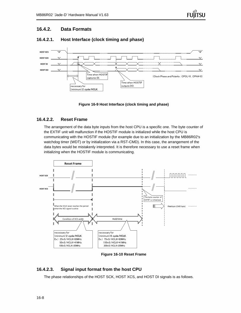
16-8
MB86R02 ‘Jade-D’ Hardware Manual V1.63
16.4.2. Data Formats
16.4.2.1. Host Interface (clock timing and phase)
"H"
"L"
"L"
"L"
"H"
"L"
"L"
"L"
Time when HOSTIF
captures DI.
Time when HOSTIF
outputs DO.
(Clock Phase and Polarity : CPOL=0 , CPHA=0)
HOST SCK
HOST XCS
HOST DI
HOST DO
necessary for
(minimum) 2 cycle/HCLK.
Figure 16-9 Host Interface (clock timing and phase)
16.4.2.2. Reset Frame
The arrangement of the data byte inputs from the host CPU is a specific one. The byte counter of the EXTIF unit will malfunction if the HOSTIF module is initialized while the host CPU is communicating with the HOSTIF module (for example due to an initialization by the MB86R02's watchdog timer (WDT) or by initialization via a RST-CMD). In this case, the arrangement of the data bytes would be mistakenly interpreted. It is therefore necessary to use a reset frame when initializing when the HOSTIF module is communicating.
HOST XCS
When the SCLK never reaches the period when the XCS signal is active
Firstbyte (CMD byte)
Condition of XCS width Hold time
Reset Frame
HOST SCK
The byte counter of
EXTIF is initialized.
necessary for
(minimum) 2 cycle/HCLK.
Ex.) 25nS/HCLK=83MHz
50nS/HCLK=41MHz100nS/HCLK=20MHz
necessary for
(minimum) 6 cycle/HCLK.
Ex.) 75nS/HCLK=83MHz
150nS/HCLK=41MHz300nS/HCLK=20MHz
Figure 16-10 Reset Frame
16.4.2.3. Signal input format from the host CPU
The phase relationships of the HOST SCK, HOST XCS, and HOST DI signals is as follows.
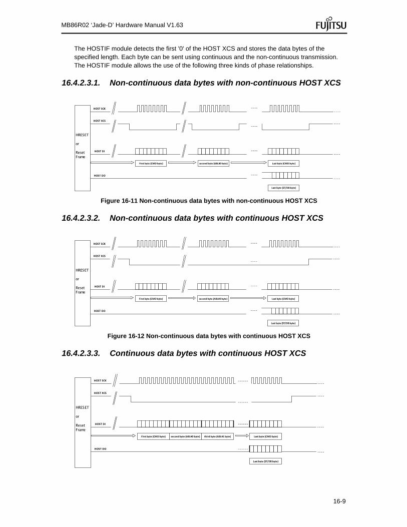
16-9
MB86R02 ‘Jade-D’ Hardware Manual V1.63
The HOSTIF module detects the first '0' of the HOST XCS and stores the data bytes of the specified length. Each byte can be sent using continuous and the non-continuous transmission. The HOSTIF module allows the use of the following three kinds of phase relationships.
16.4.2.3.1. Non-continuous data bytes with non-continuous HOST XCS
HOST DO
HOST DI
HOST XCS
HOST SCK
First byte (CMD byte) second byte (ABL#0 byte) Last byte (CMD byte)
HRESET
or
ResetFrame
Last byte (ST/DB byte)
Figure 16-11 Non-continuous data bytes with non-continuous HOST XCS
16.4.2.3.2. Non-continuous data bytes with continuous HOST XCS
HOST DO
HOST DI
HOST XCS
HOST SCK
First byte (CMD byte) second byte (ABL#0 byte) Last byte (CMD byte)
HRESET
or
ResetFrame
Last byte (ST/DB byte)
Figure 16-12 Non-continuous data bytes with continuous HOST XCS
16.4.2.3.3. Continuous data bytes with continuous HOST XCS
HOST DO
HOST DI
HOST XCS
HOST SCK
First byte (CMD byte) second byte (ABL#0 byte) Last byte (CMD byte)third byte (ABL#1 byte)
Last byte (ST/DB byte)
HRESET
or
ResetFrame
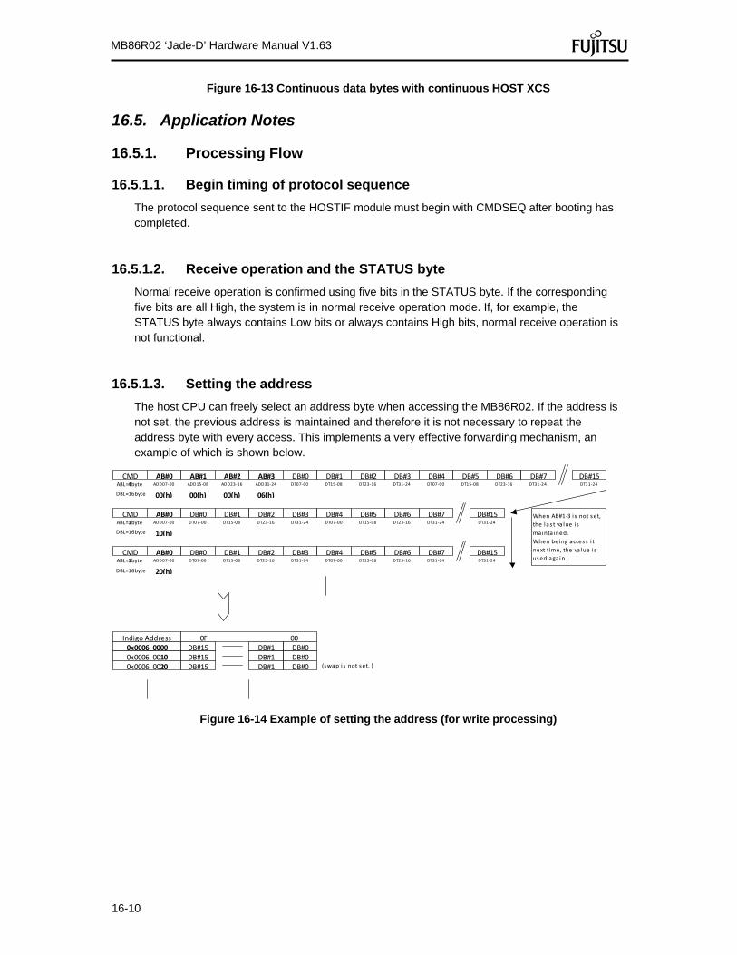
16-10
MB86R02 ‘Jade-D’ Hardware Manual V1.63
Figure 16-13 Continuous data bytes with continuous HOST XCS
16.5. Application Notes
16.5.1. Processing Flow
16.5.1.1. Begin timing of protocol sequence
The protocol sequence sent to the HOSTIF module must begin with CMDSEQ after booting has completed.
16.5.1.2. Receive operation and the STATUS byte
Normal receive operation is confirmed using five bits in the STATUS byte. If the corresponding five bits are all High, the system is in normal receive operation mode. If, for example, the STATUS byte always contains Low bits or always contains High bits, normal receive operation is not functional.
16.5.1.3. Setting the address
The host CPU can freely select an address byte when accessing the MB86R02. If the address is not set, the previous address is maintained and therefore it is not necessary to repeat the address byte with every access. This implements a very effective forwarding mechanism, an example of which is shown below.
(swap i s not set. )
ABL=4byte
CMD
DBL=16byte
ADD07‐00 ADD15‐08 ADD23‐16 ADD31‐24 DT07‐00 DT15‐08 DT23‐16 DT31‐24
AB#0 AB#1 AB#2 AB#3 DB#0 DB#1 DB#2 DB#3
ABL=1byte
CMDADD07‐00 DT07‐00 DT15‐08 DT23‐16 DT31‐24
AB#0 DB#0 DB#1 DB#2 DB#3
ABL=1byte
CMDADD07‐00 DT07‐00 DT15‐08 DT23‐16 DT31‐24
AB#0 DB#0 DB#1 DB#2 DB#3
06(h)00(h)00(h)00(h)
10(h)
20(h)
DT07‐00 DT15‐08 DT23‐16 DT31‐24
DB#4 DB#5 DB#6 DB#7DT31‐24
DB#15
DBL=16byte
DBL=16byte
DT07‐00 DT15‐08 DT23‐16 DT31‐24
DB#4 DB#5 DB#6 DB#7DT31‐24
DB#15
DT07‐00 DT15‐08 DT23‐16 DT31‐24
DB#4 DB#5 DB#6 DB#7DT31‐24
DB#15
0x0006_00000F 00
DB#15 DB#0DB#10x0006 0010 DB#15 DB#0DB#10x0006 0020 DB#15 DB#0DB#1
Indigo Address
When AB#1‐3 i s not set,
the la s t va lue is
mainta ined.
When being access i t
next time, the va lue i s
used again.
Figure 16-14 Example of setting the address (for write processing)
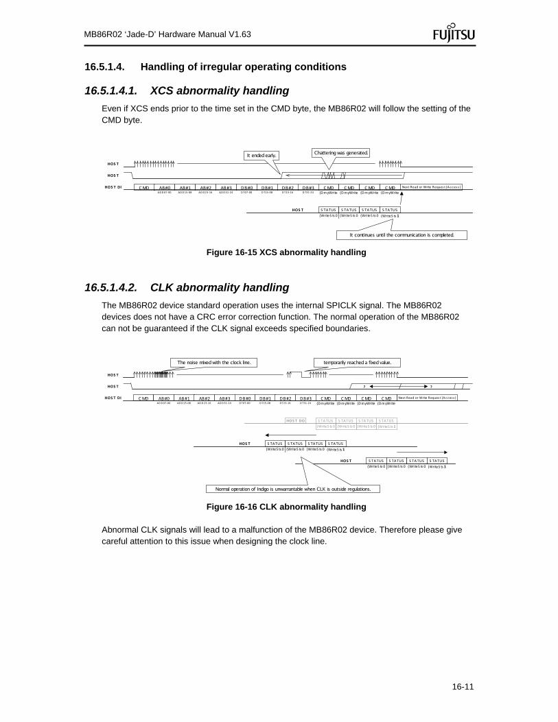
16-11
MB86R02 ‘Jade-D’ Hardware Manual V1.63
16.5.1.4. Handling of irregular operating conditions
16.5.1.4.1. XCS abnormality handling
Even if XCS ends prior to the time set in the CMD byte, the MB86R02 will follow the setting of the CMD byte.
(DmyWrite
(WriteS ts 0 (WriteS ts 1(WriteS ts 0 (WriteS ts 0
HOS T
ADD07‐00 ADD15‐08 ADD23‐16 ADD31‐24 DT07‐00 D T15‐08 DT23‐16 D T31‐24
CMD AB#0 AB#1 AB#2 AB#3 DB#0 DB#1 DB#2 DB#3
HOS T
HOS T
HOS T DI CMD Next Read or Write Reques t (A cces s )
S TATUS S TATUS S TATUS S TATUS
(DmyWriteCMD
(DmyWriteC MD
(DmyWriteCMD
It ended early. Chattering was generated.
It continues until the communication is completed.
Figure 16-15 XCS abnormality handling
16.5.1.4.2. CLK abnormality handling
The MB86R02 device standard operation uses the internal SPICLK signal. The MB86R02 devices does not have a CRC error correction function. The normal operation of the MB86R02 can not be guaranteed if the CLK signal exceeds specified boundaries.
(DmyWrite
(WriteS ts 0 (WriteS ts 1(WriteS ts 0 (WriteS ts 0
HOS T DO
ADD07‐00 ADD 15‐08 ADD 23‐16 ADD31‐24 D T07‐00 DT15‐08 D T23‐16 DT31‐24
C MD AB#0 AB#1 AB#2 AB#3 DB#0 DB#1 DB#2 DB#3
HOS T
HOS T
HOS T DI CMD Next Read or Write Reques t (A cces s )
S TATUS S TATUS S TATUS S TATUS
(DmyWriteC MD
(DmyWriteCMD
(DmyWriteC MD
The noise mixed with the clock line. temporarily reached a fixed value.
(WriteS ts 0 (WriteS ts 1(WriteS ts 0 (WriteS ts 0
HOS T S TATUS S TATUS S TATUS S TATUS
(WriteS ts 0 (WriteS ts 1(WriteS ts 0 (WriteS ts 0
HOS T S TATUS S TATUS S TATUS S TATUS
??
Normal operation of Indigo is unwarrantable when CLK is outside regulations.
Figure 16-16 CLK abnormality handling Abnormal CLK signals will lead to a malfunction of the MB86R02 device. Therefore please give careful attention to this issue when designing the clock line.

16-12
MB86R02 ‘Jade-D’ Hardware Manual V1.63
16.5.1.4.3. The first CMD is a dummy command
When the first CMD is a dummy write, the STATUS byte is immediately returned. The status is different depending on whether a READ or WRITE is returned. At this point in time, the transaction is not issued to the AHB. After the STATUS byte replies, this forwarding transaction is completed.
16.1.1.1.1 When the first CMD is a dummy Write (R/W bit=WRITE)
TxRDY is sent back for dummy WRITE CMD. Refer to Figure Error! No text of specified style in document.
Dummy Write
(Wri teSts1)
HOST DO
CMD
HOST SCK
HOST XCS
HOST DI
STATUS
Dummy Write! (Write) Rx
RDY
Tx
RDYSERR
ABL1 ABL0 DBL2 DBL1 DBL0 R/W CNT1 CNT0
Write
Wri teSts1
x 00 0 0 1 0x
0 1 10 1 1 1 1
Figure 16-17 Dummy Write (R/W bit=WRITE)
16.1.1.1.2 When the first CMD is a dummy Read (R/W bit=Read)
RxRDY is sent back for dummy READ CMD. Refer to Figure Error! No text of specified style in document.
(ReadSts1)
HOST DO
CMD
HOST SCK
HOST XCS
HOST DI
STATUS
Dummy Write! (Read)
Dummy Write
Rx
RDY
Tx
RDYSERR
ABL1 ABL0 DBL2 DBL1 DBL0 R/W CNT1 CNT0
Read
ReadSts1
x 00 0 0 0 0x
01 10 1 1 1 1
Figure 16-18 Dummy Read (R/W bit= READ)
16.5.1.4.4. The first CMD is a reset request
If the first CMD is a dummy RESET command, the HOSTIF module is reset at once although the response has begun. Please send the reset frame after the reset request.

16-13
MB86R02 ‘Jade-D’ Hardware Manual V1.63
RESET
HOST DO
CMD
HOST SCK
HOST XCS
HOST DI
S
Reset
Rx
RDY
ABL1 ABL0 DBL2 DBL1 DBL0 R/W CNT1 CNT0
x x
x
1 0x
RESET RESET
x x x
Figure 16-19 Reset Request
16.5.1.4.5. Deadlock Scenario
16.1.1.1.3 Situation recognition and recommendations
This section describes a deadlock scenario (at internal points and in the interfaces) of the MB86R02.
HOST HOST-IF AHB Slave
Slave
D.L point R1 D.L point R2 D.L point R3
D.L point T1
D.L point T2D.L point T3
SoftTIMER
CRG
CMDSEQ
TIMER
CCNT
Figure 16-20 Deadlock locations (points)
D.L point R1D.L point R2D.L point R3D.L point T1D.L point T2D.L point T3
in HOST or IFin HOST-IFin AHB BUS
HOST-IF AHB Status to HOSTIdol Idol don't send
Deadlock detectionWDT
Idol or Deadlockwaiting resp send wait Sts0
Cause ofDeadlock
in Slavein AHB BUS
waiting resp waiting resp send wait Sts0
Deadlockpoint
waiting resp send wait Sts0Idol or Deadlock
The MB86R02 device signals the completion of a normal access via the STATUS byte. If a deadlock situation occurs, the device can be automatically recovered using a watchdog (WDT) mechanism. The command list can be used to select whether watchdog reactivation is executed or not. It is also possible to monitor a MB86R02 deadlock using the timer under the control of the host CPU software. The host CPU can reset the MB86R02 by using a CMD byte. We strongly recommend that you use a host CPU issued reset because the the host CPU can not detect a

16-14
MB86R02 ‘Jade-D’ Hardware Manual V1.63
WDT issued reset. The host CPU should therefore detect abnormal operation of the MB86R02 and reacivate it itself.
16.5.1.4.6. Reactivation process
If the status is not returned because the AHB-BUS and the slave device are deadlocked, the host CPU can insert an RST request in the CMD byte during transmission. The figure below shows the deadlock reactivation process.
"0""1"XXXXXX
CMD AB#n(DmyWri te
CMD(DmyWrite
CMD(DmyWri te
CMD(DmyWrite
CMD(DmyWri te
CMD(DmyWrite
CMD
The deadlock happened !!
(DmyWri te
CMD
The response is being waited for with the software timer
ReadSts0
STATUS
ReadSts0
STATUS
ReadSts0
STATUS
ReadSts0
STATUS
ReadSts0
STATUS
ReadSts0
STATUS
ReadSts0
STATUS
(DmyWrite
CMD(DmyWrite
CMD
ReadSts0
STATUS
ReadSts0
STATUS
(RST req)
CMD
ReadSts0
STATUS STA
Start
Software TIMER of HOST
Reboot
IndigoABL1 ABL0 DBL2 DBL1 DBL0 R/W CNT1 CNT0
t
Beginning ofdata transfer
Reset isdemanded.
Time out!(e.g 0.5sec) The software timerdetects there is no response from Indigo.
Start ofsoftware timer
ResetFrame
<‐‐ Control with software
Figure 16-21 Deadlock reactivation process The response from the HOSTIF module is monitored using the software timer which is managed by the host CPU. The MB86R02 is reactivated from a deadlock by asserting a RST from the host CPU if there has been no response for a set time (e.g. for 0.5 seconds).

17-1
MB86R02 ‘Jade-D’ Hardware Manual V1.63
17 APIX® Interface This chapter describes the MB86R02 APIX interface.
17.1 Outline
MB86R02 provides two APIX interfaces. Each can be configured as APIX transmitter or receiver and is compliant to the Inova APIX® Industrial Standard.
17.2 Features
The APIX interface has following features:
17.2.1.1 APIX® PHY
The APIX® PHY provides a high speed serial downstream link and a low speed serial upstream link compliant to the Inova APIX® Industrial Standard. The downstream link transports video or generic data and side-band data. The upstream link transports side-band data only. Details can be found in document “APIX® Automotive Pixel Link Industrial Standard Rev. 1.0” The downstream link provides the following Bandwidth Modes
Full Bandwidth Mode (1000 Mbit/s) Half Bandwidth Mode (500 Mbit/s) Low bandwidth Mode 1 (125 Mbit/s) Low bandwidth Mode 2 (250 Mbit/s) One single video channel
Further features of the APIX® PHY module are
Establishment and maintenance of serial frame alignment Framing/deframing serial frames Line coding and DC balancing Serialization/deserialization
17.2.1.2 APIX® Ashell
The APIX® Automotive Shell (Ashell®) provides a secured bidirectional communication path for control data. The following key functions are offered.
Convenient wrapping of APIX® PHY's interface Transaction framing and de-framing Establishment and maintenance of transaction alignment Exchange of transactions utilizing services of APIX® PHY Bit Error Detection Bit error management
Details can be found in document “APIX® Automotive Pixel Link Industrial Standard Rev. 1.0”

17-2
MB86R02 ‘Jade-D’ Hardware Manual V1.63
17.2.1.3 Jade-D Restrictions
Only a single channel video interface is supported by one APIX PHY.
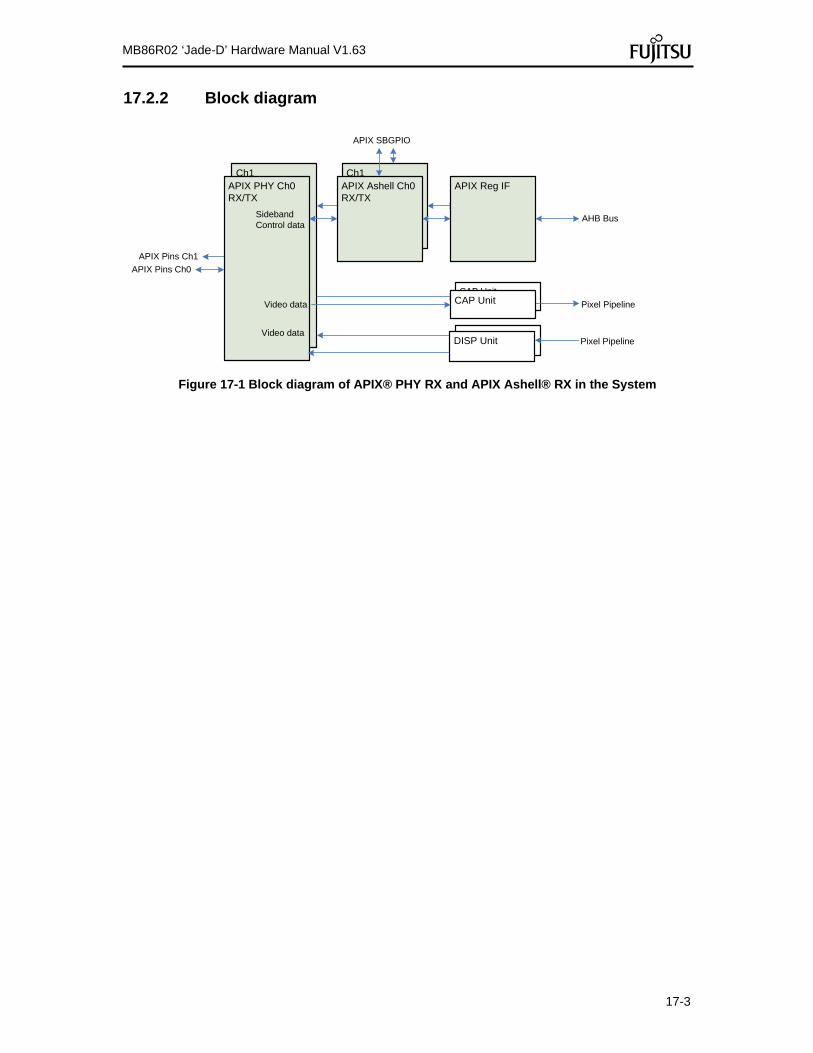
17-3
MB86R02 ‘Jade-D’ Hardware Manual V1.63
17.2.2 Block diagram
DISP Unit
CAP Unit
Ch1Ch1APIX PHY Ch0RX/TX
APIX Ashell Ch0RX/TX
CAP Unit
AHB Bus
Pixel Pipeline
APIX Pins Ch0
Sideband Control data
Video data
Video dataDISP Unit Pixel Pipeline
APIX Reg IF
APIX Pins Ch1
APIX SBGPIO
Figure 17-1 Block diagram of APIX® PHY RX and APIX Ashell® RX in the System

17-4
MB86R02 ‘Jade-D’ Hardware Manual V1.63
17.3 Software Interface
17.3.1 Format of Register Description
The register descriptions in the following sections use the format shown below to describe each bit field of a register. Register address Offset
Bit number 31 30 29 28 27 26 25 24 23 22 21 20 19 18 17 16 15 14 13 12 11 10 9 8 7 6 5 4 3 2 1 0
Field name
R/W
Reset value
Meaning of items and sign Register address
Register address shows the address (Offset address) of the register. Bit number
Bit number shows bit position of the register. Field name
Field name shows bit name of the register. R/W
R/W shows the read/write attribute of each bit field: R: Read W: Write W1C: Writing a value of "1" clears the register.
Reset value Reset value indicates the value of each bit field immediately after reset. 0: Initial value is "0". 1: Initial value is "1". X: Undefined.
Unused register fields are marked with a solid grey background. Bit vectors are unsigned integers, if nothing else specified. Please note, that access to an address with no register results in an error response.
17.3.2 Global Address
For module base address refer to inter-module specification or global address map of the respective LSI.

17-5
MB86R02 ‘Jade-D’ Hardware Manual V1.63
17.3.3 Register Summary
Address Register Name Description Base address + 0H CH0CFG Channel 0 Config Base address + 4H T0CFG0 Channel 0 TX APIX configuration byte 1-4 Base address + 8H T0CFG1 Channel 0 TX APIX configuration byte 5-8 Base address + CH T0CFG2 Channel 0 TX APIX configuration byte 9-11 Base address + 10H T0CFG3 Channel 0 TX APIX SHELL configuration byte1-4 Base address + 14H T0CFG4 Channel 0 TX APIX configuration Base address + 18H T0CTRL Channel 0 TX control Base address + 1CH T0STS0 Channel 0 TX status register 0 Base address + 20H T0STS1 Channel 0 TX status register 1 Base address + 24H R0CFG0 Channel 0 RX APIX configuration byte 1-4 Base address + 28H R0CFG1 Channel 0 RX APIX configuration byte 5-7 Base address + 2CH R0CFG2 Channel 0 RX APIX SHELL configuration byte 1-4 Base address + 34H R0CTRL Channel 0 RX control Base address + 38H R0STS0 Channel 0 RX status register 0 Base address + 3CH R0STS1 Channel 0 RX status register 1 Base address + 40H CH1CFG Channel 1 Config Base address + 44H T1CFG0 Channel 1 TX APIX configuration byte 1-4 Base address + 48H T1CFG1 Channel 1 TX APIX configuration byte 5-8 Base address + 4CH T1CFG2 Channel 1 TX APIX configuration byte 9-11 Base address + 50H T1CFG3 Channel 1 TX APIX SHELL configuration byte1-4 Base address + 54H T1CFG4 Channel 1 TX APIX configuration channel 1 Base address + 58H T1CTRL Channel 1 TX control Base address + 5CH T1STS0 Channel 1 TX status register 0 Base address + 60H T1STS1 Channel 1 TX status register 1 Base address + 64H R1CFG0 Channel 1 RX APIX configuration byte 1-4 Base address + 68H R1CFG1 Channel 1 RX APIX configuration byte 5-7 Base address + 6CH R1CFG2 Channel 1 RX APIX SHELL configuration byte 1-4 Base address + 74H R1CTRL Channel 1 RX 0 control Base address + 78H R1STS0 Channel 1 RX status register 0 Base address + 7CH R1STS1 Channel 1 RX status register 1 Base address + 100H COMPHYCFG0 Common APIX configuration 0 Base address + 104H COMPHYCFG1 Common APIX configuration 1 Base address + 10CH APPLLCFG PLL/Oscillator configuration
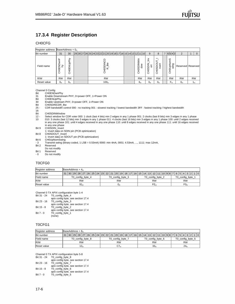
17-6
MB86R02 ‘Jade-D’ Hardware Manual V1.63
17.3.4 Register Description
CH0CFG
Register address BaseAddress + 0H
Bit number 31 30 29 28 27 26 25 24 23 22 21 20 19 18 17 16 15 14 13 12 11 10 9 8 7 6 5 4 3 2 1 0
Field name
CH
0EN
Dw
nPhy
CH
0E
NU
pPhy
CH
0SD
INC
DR
_Bw
CH
0S
DIN
Win
dow
CH
0SD
IN_I
nve
rt
CH
0SD
OU
T_I
nver
t
CH
0UpN
omS
win
g
Reserved Reserved
R/W RW RW RW RW RW RW RW RW RW
Reset value 0H 0H 100H 6H 0H 0H FH 0H 1H
Channel 0 Config Bit 31
CH0ENDwnPhy Enable Downstream PHY, 0=power OFF, 1=Power ON
Bit 30
CH0ENUpPhy Enable Upstream PHY, 0=power OFF, 1=Power ON
Bit 25 - 16
CH0SDINCDR_Bw CDR bandwidth control 000 : no tracking 001 : slowest tracking / lowest bandwidth 3FF : fastest tracking / highest bandwidth
Bit 12 - 10
CH0SDINWindow Select window for CDR voter 000: 1 clock (last 4 bits) min 2 edges in any 1 phase 001: 2 clocks (last 8 bits) min 3 edges in any 1 phase 010: 3 clocks (last 12 bits) min 3 edges in any 1 phase 011: 4 clocks (last 16 bits) min 3 edges in any 1 phase 100: until 2 edges received in any one phase 101: until 4 edges received in any one phase 110: until 8 edges received in any one phase 111: until 16 edges received in any one phase
Bit 9 CH0SDIN_Invert 1: Invert data on SDIN pin (PCB optimization)
Bit 8 CH0SDOUT_Invert 1: Invert data on SDOUT pin (PCB optimization)
Bit 6 - 3
CH0UpNomSwing Transmit swing (binary coded, 1 LSB = 0.53mA) 0000: min 4mA, 0001: 4.53mA, ..., 1111: max 12mA,
Bit 2 Reserved Do not modify
Bit 1 - 0
Reserved Do not modify
T0CFG0
Register address BaseAddress + 4H
Bit number 31 30 29 28 27 26 25 24 23 22 21 20 19 18 17 16 15 14 13 12 11 10 9 8 7 6 5 4 3 2 1 0
Field name T0_config_byte_4 T0_config_byte_3 T0_config_byte_2 T0_config_byte_1
R/W RW RW RW RW
Reset value 91H 0H FEH F0H
Channel 0 TX APIX configuration byte 1-4 Bit 31 - 24 T0_config_byte_4
apix config byte, see section 17.4 Bit 23 - 16 T0_config_byte_3
apix config byte, see section 17.4 Bit 15 - 8 T0_config_byte_2
apix config byte, see section 17.4 Bit 7 - 0 T0_config_byte_1
(none)
T0CFG1
Register address BaseAddress + 8H
Bit number 31 30 29 28 27 26 25 24 23 22 21 20 19 18 17 16 15 14 13 12 11 10 9 8 7 6 5 4 3 2 1 0
Field name T0_config_byte_8 T0_config_byte_7 T0_config_byte_6 T0_config_byte_5
R/W RW RW RW RW
Reset value 12H C7H 33H 24H
Channel 0 TX APIX configuration byte 5-8 Bit 31 - 24 T0_config_byte_8
apix config byte, see section 17.4 Bit 23 - 16 T0_config_byte_7
apix config byte, see section 17.4 Bit 15 - 8 T0_config_byte_6
apix config byte, see section 17.4 Bit 7 - 0 T0_config_byte_5
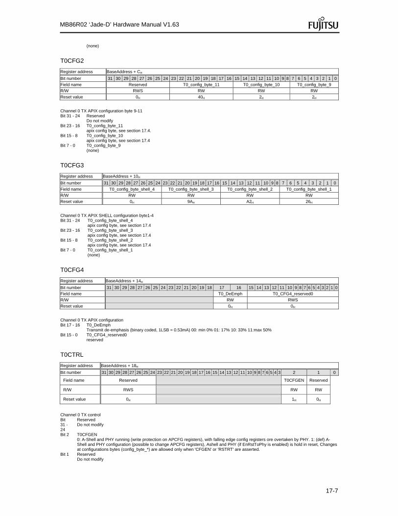
17-7
MB86R02 ‘Jade-D’ Hardware Manual V1.63
(none)
T0CFG2
Register address BaseAddress + CH
Bit number 31 30 29 28 27 26 25 24 23 22 21 20 19 18 17 16 15 14 13 12 11 10 9 8 7 6 5 4 3 2 1 0
Field name Reserved T0_config_byte_11 T0_config_byte_10 T0_config_byte_9
R/W RWS RW RW RW
Reset value 0H 40H 2H 2H
Channel 0 TX APIX configuration byte 9-11 Bit 31 - 24 Reserved
Do not modify Bit 23 - 16 T0_config_byte_11
apix config byte, see section 17.4. Bit 15 - 8 T0_config_byte_10
apix config byte, see section 17.4 Bit 7 - 0 T0_config_byte_9
(none)
T0CFG3
Register address BaseAddress + 10H
Bit number 31 30 29 28 27 26 25 24 23 22 21 20 19 18 17 16 15 14 13 12 11 10 9 8 7 6 5 4 3 2 1 0
Field name T0_config_byte_shell_4 T0_config_byte_shell_3 T0_config_byte_shell_2 T0_config_byte_shell_1
R/W RW RW RW RW
Reset value 0H 9AH A2H 26H
Channel 0 TX APIX SHELL configuration byte1-4 Bit 31 - 24 T0_config_byte_shell_4
apix config byte, see section 17.4 Bit 23 - 16 T0_config_byte_shell_3
apix config byte, see section 17.4 Bit 15 - 8 T0_config_byte_shell_2
apix config byte, see section 17.4 Bit 7 - 0 T0_config_byte_shell_1
(none)
T0CFG4
Register address BaseAddress + 14H
Bit number 31 30 29 28 27 26 25 24 23 22 21 20 19 18 17 16 15 14 13 12 11 10 9 8 7 6 5 4 3 2 1 0
Field name T0_DeEmph T0_CFG4_reserved0
R/W RW RWS
Reset value 0H 0H
Channel 0 TX APIX configuration Bit 17 - 16 T0_DeEmph
Transmit de-emphasis (binary coded, 1LSB = 0.53mA) 00: min 0% 01: 17% 10: 33% 11:max 50% Bit 15 - 0 T0_CFG4_reserved0
reserved
T0CTRL
Register address BaseAddress + 18H
Bit number 31 30 29 28 27 26 25 24 23 22 21 20 19 18 17 16 15 14 13 12 11 10 9 8 7 6 5 4 3 2 1 0
Field name Reserved T0CFGEN Reserved
R/W RWS RW RW
Reset value 0H 1H 0H
Channel 0 TX control Bit 31 - 24
Reserved Do not modify
Bit 2 T0CFGEN 0: A-Shell and PHY running (write protection on APCFG registers), with falling edge config registers ore overtaken by PHY. 1: (def) A-Shell and PHY configuration (possible to change APCFG registers), Ashell and PHY (if EnRstToPhy is enabled) is hold in reset, Changes at configurations bytes (config_byte_*) are allowed only when 'CFGEN' or 'RSTRT' are asserted.
Bit 1 Reserved Do not modify
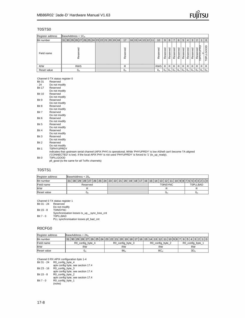
17-8
MB86R02 ‘Jade-D’ Hardware Manual V1.63
T0STS0
Register address BaseAddress + 1CH
Bit number 31 30 29 28 27 26 25 24 23 22 21 20 19 18 17 16 15 14 13 12 11 10 9 8 7 6 5 4 3 2 1 0
Field name
Res
erve
d
Res
erve
d
Res
erve
d
Res
erve
d
Res
erve
d
Res
erve
d
Res
erve
d
Res
erve
d
Res
erve
d
Res
erve
d
Res
erve
d
T0P
HY
UP
RD
YT
0PLL
GO
OD
R/W RWS R RWS R R R R R R R R R R
Reset value 0H 0H 0H 0H 0H 0H 0H 0H 0H 0H 0H 0H 0H
Channel 0 TX status register 0 Bit 31 - 24
Reserved Do not modify
Bit 17 Reserved Do not modify
Bit 10 Reserved Do not modify
Bit 9 Reserved Do not modify
Bit 8 Reserved Do not modify
Bit 7 Reserved Do not modify
Bit 6 Reserved Do not modify
Bit 5 Reserved Do not modify
Bit 4 Reserved Do not modify
Bit 3 Reserved Do not modify
Bit 2 Reserved Do not modify
Bit 1 T0PHYUPRDY indicates that upstream serial channel (APIX PHY) is operational, While 'PHYUPRDY' is low AShell can't become TA aligned ('CONNECTED' is low). If the local APIX PHY is not used 'PHYUPRDY' is forced to '1' (tx_up_ready).
Bit 0 T0PLLGOOD pll_good (is the same for all Tx/Rx channels)
T0STS1
Register address BaseAddress + 20H
Bit number 31 30 29 28 27 26 25 24 23 22 21 20 19 18 17 16 15 14 13 12 11 10 9 8 7 6 5 4 3 2 1 0
Field name Reserved T0INSYNC T0PLLBAD
R/W R R R
Reset value 0H 0H 0H
Channel 0 TX status register 1 Bit 31 - 24 Reserved
Do not modify Bit 15 - 8 T0INSYNC
Synchronisation losses tx_up__sync_loss_cnt Bit 7 - 0 T0PLLBAD
PLL synchronisation losses pll_bad_cnt
R0CFG0
Register address BaseAddress + 24H
Bit number 31 30 29 28 27 26 25 24 23 22 21 20 19 18 17 16 15 14 13 12 11 10 9 8 7 6 5 4 3 2 1 0
Field name R0_config_byte_4 R0_config_byte_3 R0_config_byte_2 R0_config_byte_1
R/W RW RW RW RW
Reset value 0H 86H BCH 3DH
Channel 0 RX APIX configuration byte 1-4 Bit 31 - 24 R0_config_byte_4
apix config byte, see section 17.4 Bit 23 - 16 R0_config_byte_3
apix config byte, see section 17.4 Bit 15 - 8 R0_config_byte_2
apix config byte, see section 17.4 Bit 7 - 0 R0_config_byte_1
(none)

17-9
MB86R02 ‘Jade-D’ Hardware Manual V1.63
R0CFG1
Register address BaseAddress + 28H
Bit number 31 30 29 28 27 26 25 24 23 22 21 20 19 18 17 16 15 14 13 12 11 10 9 8 7 6 5 4 3 2 1 0
Field name Reserved R0_config_byte_7 R0_config_byte_6 R0_config_byte_5
R/W RWS RW RW RW
Reset value 0H 93H C0H 3FH
Channel 0 RX APIX configuration byte 5-7 Bit 31 - 24 Reserved
Do not modify Bit 23 - 16 R0_config_byte_7
apix config byte, see section 17.4 Bit 15 - 8 R0_config_byte_6
apix config byte, see section 17.4 Bit 7 - 0 R0_config_byte_5
(none)
R0CFG2
Register address BaseAddress + 2CH
Bit number 31 30 29 28 27 26 25 24 23 22 21 20 19 18 17 16 15 14 13 12 11 10 9 8 7 6 5 4 3 2 1 0
Field name R0_config_byte_shell_4 R0_config_byte_shell_3 R0_config_byte_shell_2 R0_config_byte_shell_1
R/W RW RW RW RW
Reset value A0H 9H 89H 0H
Channel 0 RX APIX SHELL configuration byte 1-4 Bit 31 - 24 R0_config_byte_shell_4
apix config byte, see section 17.4 Bit 23 - 16 R0_config_byte_shell_3
apix config byte, see section 17.4 Bit 15 - 8 R0_config_byte_shell_2
apix config byte, see section 17.4 Bit 7 - 0 R0_config_byte_shell_1
(none)
R0CTRL
Register address BaseAddress + 34H
Bit number 31 30 29 28 27 26 25 24 23 22 21 20 19 18 17 16 15 14 13 12 11 10 9 8 7 6 5 4 3 2 1 0
Field name Reserved R0CFGEN Reserved
R/W RWS RW RW
Reset value 0H 1H 0H
Channel 0 RX control Bit 31 - 24
Reserved Do not modify
Bit 2 R0CFGEN 0: A-Shell and PHY running (write protection on APCFG registers), with falling edge config registers ore overtaken by PHY. 1: (def) A-Shell and PHY configuration (possible to change APCFG registers), Ashell and PHY (if EnRstToPhy is enabled) is hold in reset, Changes at configurations bytes (config_byte_*) are allowed only when 'CFGEN' or 'RSTRT' are asserted.
Bit 1 Reserved Do not modify
R0STS0
Register address BaseAddress + 38H
Bit number 31 30 29 28 27 26 25 24 23 22 21 20 19 18 17 16 15 14 13 12 11 10 9 8 7 6 5 4 3 2 1 0
Field name
Res
erve
d
Res
erve
d
R0
PX
ALI
GN
D
Res
erve
d
Res
erve
d
Res
erve
d
Res
erve
d
Res
erve
d
Res
erve
d
Res
erve
d
Res
erve
d
R0P
HY
DW
NR
DY R0PLLGOOD
R/W RWS R R R R R R R R R R R R
Reset value 0H 0H 0H 0H 0H 0H 0H 0H 0H 0H 0H 0H 0H
Channel 0 RX status register 0 Bit 31 - 24
Reserved Do not modify

17-10
MB86R02 ‘Jade-D’ Hardware Manual V1.63
Bit 17 Reserved Do not modify
Bit 10 R0PXALIGND rx_pix_aligned, 1=Pixel link operational
Bit 9 Reserved Do not modify
Bit 8 Reserved Do not modify
Bit 7 Reserved Do not modify
Bit 6 Reserved Do not modify
Bit 5 Reserved Do not modify
Bit 4 Reserved Do not modify
Bit 3 Reserved Do not modify
Bit 2 Reserved Do not modify
Bit 1 R0PHYDWNRDY indicates that downstream serial channel (APIX PHY) is operational, While 'PHYDWNRDY' is low AShell can't become TA aligned ('CONNECTED' is low). If the local APIX PHY is not used 'PHYDWNRDY' is forced to '1' (rx_down_ready).
Bit 0 R0PLLGOOD pll_good (is the same for all Tx/Rx channels)
R0STS1
Register address BaseAddress + 3CH
Bit number 31 30 29 28 27 26 25 24 23 22 21 20 19 18 17 16 15 14 13 12 11 10 9 8 7 6 5 4 3 2 1 0
Field name Reserved R0Eye R0INSYNC R0PLLBAD
R/W R R R R
Reset value 0H X 0H 0H
Channel 0 RX status register 1 Bit 31 - 24 Reserved
Do not modify Bit 20 - 16 R0Eye
Measured eye opening, 1=edge in this phase during measurement period was set by Eyetime Bit 15 - 8 R0INSYNC
Synchronisation losses rx_down__sync_loss_cnt Bit 7 - 0 R0PLLBAD
PLL synchronisation losses pll_bad_cnt
CH1CFG
Register address BaseAddress + 40H
Bit number 31 30 29 28 27 26 25 24 23 22 21 20 19 18 17 16 15 14 13 12 11 10 9 8 7 6 5 4 3 2 1 0
Fie
ld n
ame
CH
1EN
Dw
nP
hy
CH
1EN
UpP
hy
CH
1SD
INC
DR
_Bw
CH
1SD
INW
indo
w
CH
1SD
IN_I
nver
t
CH
1SD
OU
T_I
nve
rt
CH
1UpN
omS
win
g
Res
erv
ed
Res
erv
ed
R/W RW RW RW RW RW RW RW RW RW
Reset value 0H 0H 0H 6H 0H 0H FH 0H 1H
Channel 1 Config Bit 31
CH1ENDwnPhy Enable Downstream PHY, 0=power OFF, 1=Power ON
Bit 30
CH1ENUpPhy Enable Upstream PHY, 0=power OFF, 1=Power ON
Bit 25 - 16
CH1SDINCDR_Bw Channel 1 CDR bandwidth control 000 : no tracking 001 : slowest tracking / lowest bandwidth 3FF : fastest tracking / highest bandwidth
Bit 12 - 10
CH1SDINWindow Select window for CDR voter 000: 1 clock (last 4 bits) min 2 edges in any 1 phase 001: 2 clocks (last 8 bits) min 3 edges in any 1 phase 010: 3 clocks (last 12 bits) min 3 edges in any 1 phase 011: 4 clocks (last 16 bits) min 3 edges in any 1 phase 100: until 2 edges received in any one phase 101: until 4 edges received in any one phase 110: until 8 edges received in any one phase 111: until 16 edges received in any one phase
Bit 9 CH1SDIN_Invert 1: Invert data on SDIN pin (PCB optimization)
Bit 8 CH1SDOUT_Invert 1: Invert data on SDOUT pin (PCB optimization)
Bit 6 - 3
CH1UpNomSwing Transmit swing (binary coded, 1 LSB = 0.53mA) 0000: min 4mA, 0001: 4.53mA, ..., 1111: max 12mA,
Bit 2 Reserved Do not modify
Bit 1 Reserved

17-11
MB86R02 ‘Jade-D’ Hardware Manual V1.63
- 0 Do not modify
T1CFG0
Register address BaseAddress + 44H
Bit number 31 30 29 28 27 26 25 24 23 22 21 20 19 18 17 16 15 14 13 12 11 10 9 8 7 6 5 4 3 2 1 0
Field name T1_config_byte_4 T1_config_byte_3 T1_config_byte_2 T1_config_byte_1
R/W RW RW RW RW
Reset value 91H 0H FEH F0H
channel 1 TX APIX configuration byte 1-4 Bit 31 - 24 T1_config_byte_4
apix config byte, see section 17.4 Bit 23 - 16 T1_config_byte_3
apix config byte, see section 17.4 Bit 15 - 8 T1_config_byte_2
apix config byte, s see section 17.4 Bit 7 - 0 T1_config_byte_1
(none)
T1CFG1
Register address BaseAddress + 48H
Bit number 31 30 29 28 27 26 25 24 23 22 21 20 19 18 17 16 15 14 13 12 11 10 9 8 7 6 5 4 3 2 1 0
Field name T1_config_byte_8 T1_config_byte_7 T1_config_byte_6 T1_config_byte_5
R/W RW RW RW RW
Reset value 12H C7H 33H 24H
channel 1 TX APIX configuration byte 5-8 Bit 31 - 24 T1_config_byte_8
apix config byte, see section 17.4 Bit 23 - 16 T1_config_byte_7
apix config byte, see section 17.4 Bit 15 - 8 T1_config_byte_6
apix config byte, see section 17.4 Bit 7 - 0 T1_config_byte_5
(none)
T1CFG2
Register address BaseAddress + 4CH
Bit number 31 30 29 28 27 26 25 24 23 22 21 20 19 18 17 16 15 14 13 12 11 10 9 8 7 6 5 4 3 2 1 0
Field name Reserved T1_config_byte_11 T1_config_byte_10 T1_config_byte_9
R/W RWS RW RW RW
Reset value 0H 40H 2H 2H
channel 1 TX APIX configuration byte 9-11 Bit 31 - 24 Reserved
Do not modify Bit 23 - 16 T1_config_byte_11
apix config byte, see section 17.4. Bit 15 - 8 T1_config_byte_10
apix config byte, see section 17.4 Bit 7 - 0 T1_config_byte_9
(none)
T1CFG3
Register address BaseAddress + 50H
Bit number 31 30 29 28 27 26 25 24 23 22 21 20 19 18 17 16 15 14 13 12 11 10 9 8 7 6 5 4 3 2 1 0
Field name T1_config_byte_shell_4 T1_config_byte_shell_3 T1_config_byte_shell_2 T1_config_byte_shell_1
R/W RW RW RW RW
Reset value 0H 9AH A2H 26H
channel 1 TX APIX SHELL configuration byte1-4 Bit 31 - 24 T1_config_byte_shell_4
apix config byte, see section 17.4 Bit 23 - 16 T1_config_byte_shell_3
apix config byte, see section 17.4 Bit 15 - 8 T1_config_byte_shell_2
apix config byte, see section 17.4 Bit 7 - 0 T1_config_byte_shell_1
(none)

17-12
MB86R02 ‘Jade-D’ Hardware Manual V1.63
T1CFG4
Register address BaseAddress + 54H
Bit number 31 30 29 28 27 26 25 24 23 22 21 20 19 18 17 16 15 14 13 12 11 10 9 8 7 6 5 4 3 2 1 0
Field name T1_DeEmph T1_CFG4_reserved0
R/W RW RWS
Reset value 0H 0H
Channel 1 TX APIX configuration channel 1 Bit 17 - 16 T1_DeEmph
Transmit de-emphasis (binary coded, 1LSB = 0.53mA) 00: min 0% 01: 17% 10: 33% 11:max 50% Bit 15 - 0 T1_CFG4_reserved0
reserved
T1CTRL
Register address BaseAddress + 58H
Bit number 31 30 29 28 27 26 25 24 23 22 21 20 19 18 17 16 15 14 13 12 11 10 9 8 7 6 5 4 3 2 1 0
Field name Reserved T1CFGEN Reserved
R/W RWS RW RW
Reset value 0H 1H 0H
Channel 1 TX control Bit 31 - 24
Reserved Do not modify
Bit 2 T1CFGEN 0: A-Shell and PHY running (write protection on APCFG registers), with falling edge config registers ore overtaken by PHY. 1: (def) A-Shell and PHY configuration (possible to change APCFG registers), Ashell and PHY (if EnRstToPhy is enabled) is hold in reset, Changes at configurations bytes (config_byte_*) are allowed only when 'CFGEN' or 'RSTRT' are asserted.
Bit 1 Reserved Do not modify
T1STS0
Register address BaseAddress + 5CH
Bit number 31 30 29 28 27 26 25 24 23 22 21 20 19 18 17 16 15 14 13 12 11 10 9 8 7 6 5 4 3 2 1 0
Fie
ld n
ame
Res
erv
ed
Res
erv
ed
Res
erv
ed
Res
erv
ed
Res
erv
ed
Res
erv
ed
Res
erv
ed
Res
erv
ed
Res
erv
ed
Res
erv
ed
T1P
HY
UP
RD
YT
1P
LLG
OO
D
R/W RWS R R R R R R R R R R R
Reset value 0H 0H 0H 0H 0H 0H 0H 0H 0H 0H 0H 0H
Channel 1 TX status register 0 Bit 31 - 24
Reserved Do not modify
Bit 17 Reserved Do not modify
Bit 9 Reserved Do not modify
Bit 8 Reserved Do not modify
Bit 7 Reserved Do not modify
Bit 6 Reserved Do not modify
Bit 5 Reserved Do not modify
Bit 4 Reserved Do not modify
Bit 3 Reserved Do not modify
Bit 2 Reserved Do not modify
Bit 1 T1PHYUPRDY indicates that upstream serial channel (APIX PHY) is operational, While 'PHYUPRDY' is low AShell can't become TA aligned ('CONNECTED' is low). If the local APIX PHY is not used 'PHYUPRDY' is forced to '1' (tx_up_ready).
Bit 0 T1PLLGOOD pll_good (is the same for all Tx/Rx channels)

17-13
MB86R02 ‘Jade-D’ Hardware Manual V1.63
T1STS1
Register address BaseAddress + 60H
Bit number 31 30 29 28 27 26 25 24 23 22 21 20 19 18 17 16 15 14 13 12 11 10 9 8 7 6 5 4 3 2 1 0
Field name Reserved T1INSYNC T1PLLBAD
R/W R R R
Reset value 0H 0H 0H
Channel 1 TX status register 1 Bit 31 - 24 Reserved
Do not modify Bit 15 - 8 T1INSYNC
Synchronisation losses tx_up__sync_loss_cnt Bit 7 - 0 T1PLLBAD
PLL synchronisation losses pll_bad_cnt
R1CFG0
Register address BaseAddress + 64H
Bit number 31 30 29 28 27 26 25 24 23 22 21 20 19 18 17 16 15 14 13 12 11 10 9 8 7 6 5 4 3 2 1 0
Field name R1_config_byte_4 R1_config_byte_3 R1_config_byte_2 R1_config_byte_1
R/W RW RW RW RW
Reset value 0H 86H BCH 3DH
Channel 1 RX APIX configuration byte 1-4 Bit 31 - 24 R1_config_byte_4
apix config byte, see section 17.4 Bit 23 - 16 R1_config_byte_3
apix config byte, see section 17.4 Bit 15 - 8 R1_config_byte_2
apix config byte, see section 17.4 Bit 7 - 0 R1_config_byte_1
(none)
R1CFG1
Register address BaseAddress + 68H
Bit number 31 30 29 28 27 26 25 24 23 22 21 20 19 18 17 16 15 14 13 12 11 10 9 8 7 6 5 4 3 2 1 0
Field name Reserved R1_config_byte_7 R1_config_byte_6 R1_config_byte_5
R/W RWS RW RW RW
Reset value 0H 93H C0H 3FH
channel 1 RX APIX configuration byte 5-7 Bit 31 - 24 Reserved
Do not modify Bit 23 - 16 R1_config_byte_7
apix config byte, see section 17.4 Bit 15 - 8 R1_config_byte_6
apix config byte, see section 17.4 Bit 7 - 0 R1_config_byte_5
(none)
R1CFG2
Register address BaseAddress + 6CH
Bit number 31 30 29 28 27 26 25 24 23 22 21 20 19 18 17 16 15 14 13 12 11 10 9 8 7 6 5 4 3 2 1 0
Field name R1_config_byte_shell_4 R1_config_byte_shell_3 R1_config_byte_shell_2 R1_config_byte_shell_1
R/W RW RW RW RW
Reset value A0H 9H 89H 0H
channel 1 RX APIX SHELL configuration byte 1-4 Bit 31 - 24 R1_config_byte_shell_4
apix config byte, see section 17.4 Bit 23 - 16 R1_config_byte_shell_3
apix config byte, see section 17.4 Bit 15 - 8 R1_config_byte_shell_2
apix config byte, see section 17.4 Bit 7 - 0 R1_config_byte_shell_1
(none)
R1CTRL

17-14
MB86R02 ‘Jade-D’ Hardware Manual V1.63
Register address BaseAddress + 74H
Bit number 31 30 29 28 27 26 25 24 23 22 21 20 19 18 17 16 15 14 13 12 11 10 9 8 7 6 5 4 3 2 1 0
Field name Reserved R1CFGEN Reserved
R/W RWS RW RW
Reset value 0H 1H 0H
Channel 1 RX 0 control Bit 31 - 24
Reserved Do not modify
Bit 2 R1CFGEN 0: A-Shell and PHY running (write protection on APCFG registers), with falling edge config registers ore overtaken by PHY. 1: (def) A-Shell and PHY configuration (possible to change APCFG registers), Ashell and PHY (if EnRstToPhy is enabled) is hold in reset, Changes at configurations bytes (config_byte_*) are allowed only when 'CFGEN' or 'RSTRT' are asserted.
Bit 1 Reserved Do not modify
R1STS0
Register address BaseAddress + 78H
Bit number 31 30 29 28 27 26 25 24 23 22 21 20 19 18 17 16 15 14 13 12 11 10 9 8 7 6 5 4 3 2 1 0
Fie
ld n
ame
Res
erv
ed
Res
erv
ed
R1P
XA
LIG
ND
Res
erv
ed
Res
erv
ed
Res
erv
ed
Res
erv
ed
Res
erv
ed
Res
erv
ed
Res
erv
ed
Res
erv
ed
R1P
HY
DW
NR
DY
R1P
LLG
OO
D
R/W RWS R R R R R R R R R R R R
Reset value 0H 0H 0H 0H 0H 0H 0H 0H 0H 0H 0H 0H 0H
Channel 1 RX status register 0 Bit 31 - 24
Reserved Do not modify
Bit 17 Reserved Do not modify
Bit 10 R1PXALIGND rx_pix_aligned, 1=Pixel link operational
Bit 9 Reserved Do not modify
Bit 8 Reserved Do not modify
Bit 7 Reserved Do not modify
Bit 6 Reserved Do not modify
Bit 5 Reserved Do not modify
Bit 4 Reserved Do not modify
Bit 3 Reserved Do not modify
Bit 2 Reserved Do not modify
Bit 1 R1PHYDWNRDY indicates that downstream serial channel (APIX PHY) is operational, While 'PHYDWNRDY' is low AShell can't become TA aligned ('CONNECTED' is low). If the local APIX PHY is not used 'PHYDWNRDY' is forced to '1' (rx_down_ready).
Bit 0 R1PLLGOOD pll_good (is the same for all Tx/Rx channels)
R1STS1
Register address BaseAddress + 7CH
Bit number 31 30 29 28 27 26 25 24 23 22 21 20 19 18 17 16 15 14 13 12 11 10 9 8 7 6 5 4 3 2 1 0
Field name Reserved R1Eye R1INSYNC R1PLLBAD
R/W R R R R
Reset value 0H X 0H 0H
Channel 1 RX status register 1 Bit 31 - 24 Reserved
Do not modify Bit 20 - 16 R1Eye
Measured eye opening, 1=edge in this phase during measurement period was set by Eyetime Bit 15 - 8 R1INSYNC
Synchronisation losses rx_down__sync_loss_cnt Bit 7 - 0 R1PLLBAD

17-15
MB86R02 ‘Jade-D’ Hardware Manual V1.63
PLL synchronisation losses pll_bad_cnt
COMPHYCFG0
Register address BaseAddress + 100H
Bit number 31 30 29 28 27 26 25 24 23 22 21 20 19 18 17 16 15 14 13 12 11 10 9 8 7 6 5 4 3 2 1 0
Field name COMAPCFG_reserved0 En_OffsetComp SwRstToPHY EnRstToPHY RXEyeTime
R/W RWS RW RW RW RW
Reset value 0H 0H 1H 0H 100H
common APIX configuration 0 Bit 31 - 19 COMAPCFG_reserved0
reserved Bit 18 En_OffsetComp
Enable Offset Compensation (0=power OFF, 1=power ON) Bit 17 SwRstToPHY
SW reset to PHY, 0=inactive, 1=active Bit 16 EnRstToPHY
enable reset from Ashells to PHY, 0=disabled, 1=enabled Bit 11 - 0 RXEyeTime
Measurement period for RxEye, 1lsb = 64ns (16*clk250 counts)
COMPHYCFG1
Register address BaseAddress + 104H
Bit number 31 30 29 28 27 26 25 24 23 22 21 20 19 18 17 16 15 14 13 12 11 10 9 8 7 6 5 4 3 2 1 0
Field name MiscCfg Atst_sel Mask_pll_good Reserved
R/W RW RW RW RW
Reset value 0H 0H 1H 0H
common APIX configuration 1 Bit 31 - 16 MiscCfg
reserved Bit 11 - 8 Atst_sel
Select use of ATST pad 0: not used 1: Vco control voltge 2: Bandgap voltage 3: Reference current Bit 4 Mask_pll_good
Masks pllGood for reset in digital 0: pll_good + reset_n signals used to reset digital, 1: only reset_n signal is used to reset digital Bit 3 Reserved
Do not modify
APPLLCFG
Register address
BaseAddress + 10CH
Bit number 31 30 29 28 27 26 25 24 23 22 21 20 19 18 17 16 15 14 13 12 11 10 9 8 7 6 5 4 3 2 1 0
Field name En_PLL APPLLCFG_reserved0 crgPmpCtrl PhyPllReset LoopResistor preDiv2 NDiv
R/W RW RWS RW RW RW RW RW
Reset value 0H 0H 3H 1H 3H 0H 14H
PLL/Oscilator configuration Bit 31 En_PLL
Enable PLL (0=power OFF, 1=power ON) Bit 30 - 24 APPLLCFG_reserved0
PLL/Oscilator configuration reserved Bit 23 - 20 crgPmpCtrl
Charge Pump Current Control 0000: 5uA, 0001: 10uA, ..., 1111: 80uA, Bit 12 PhyPllReset
reset the Pll of the connected PHY: 0=reset not asserted; 1=reset asserted Bit 10 - 8 LoopResistor
Resistor in PLL loop filter, 0..7: 1K, 2K, 4K, 8K, 12K, 15K, 18K ohm Bit 7 preDiv2
PLL Pre-divider reference clock by 2, 0: no division, 1: divide by 2 Bit 6 - 0 NDiv
PLL Feedback divider ratio 0,1,2,..127 => Divide by 128,128,2..127

17-16
MB86R02 ‘Jade-D’ Hardware Manual V1.63
17.4 Description of APIX Ashell and APIX PHY configuration bytes
17.4.1 RX
config_byte_1
Bit init
ial
Name Description
7 0 cfg_up_clk_divider[1]
APIX PHY upstream channel bandwidth setting bandwidth mode of downstream link 1000 Mbit/s 125 MBit/s 500 Mbit/s 00: not applicable 62.50 MBit/s1 01: 62.50 MBit/s 31.25 MBit/s 10: 41.67 MBit/s 20.83 MBit/s 11: 31.25 MBit/s not applicable
Note: upstream bandwidth setting has to match related transmitter device configuration
6 0 cfg_up_clk_divider[0]
5 1 reserved reserved
4 1 reserved
3 1 reserved
2 1 reserved
1 0 reserved
0 1 cfg_sbup_smode
APIX PHY relation of upstream sideband data to core clock of APIX PHY 0: asynchronous, 1: synchronous
Table 17-2 RX config_byte_1
1 If a setup with the external AShell is used and the external AShell is running with a 62.5 MHz core clock, then the 62.5MBit/s upstream channel bandwidth for half and low bandwidth mode is not supported.
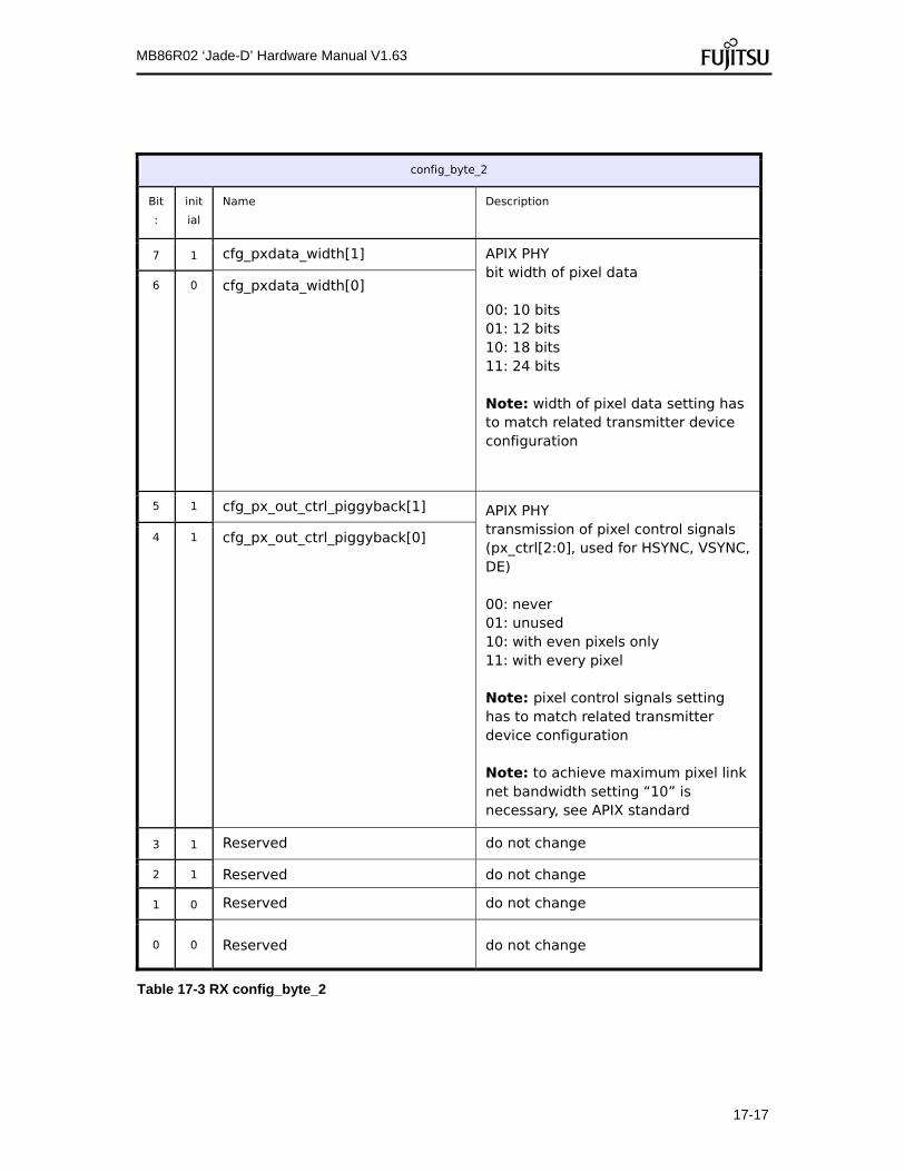
17-17
MB86R02 ‘Jade-D’ Hardware Manual V1.63
config_byte_2
Bit
:
init
ial
Name Description
7 1 cfg_pxdata_width[1] APIX PHY bit width of pixel data 00: 10 bits 01: 12 bits 10: 18 bits 11: 24 bits Note: width of pixel data setting has to match related transmitter device configuration
6 0 cfg_pxdata_width[0]
5 1 cfg_px_out_ctrl_piggyback[1] APIX PHY transmission of pixel control signals (px_ctrl[2:0], used for HSYNC, VSYNC, DE) 00: never 01: unused 10: with even pixels only 11: with every pixel Note: pixel control signals setting has to match related transmitter device configuration Note: to achieve maximum pixel link net bandwidth setting “10” is necessary, see APIX standard
4 1 cfg_px_out_ctrl_piggyback[0]
3 1 Reserved do not change
2 1 Reserved do not change
1 0 Reserved do not change
0 0 Reserved do not change
Table 17-3 RX config_byte_2

17-18
MB86R02 ‘Jade-D’ Hardware Manual V1.63
config_byte_3
Bit
:
init
ial
Name Description
7 1 reserved do not change
6 0 reserved do not change
5 0 reserved do not change
4 0 reserved
3 0 reserved
2 1 reserved do not change
1 1 reserved do not change
0 0 reserved do not change
Table 17-4 RX config_byte_3
config_byte_4
Bit
:
init
ial
Name Description
7 0 reserved do not change
6 0 reserved do not change
5 0 reserved do not change
4 0 reserved do not change
3 0 reserved do not change
2 0 reserved do not change
1 0 reserved do not change
0 0 reserved do not change
Table 17-5 RX config_byte_4
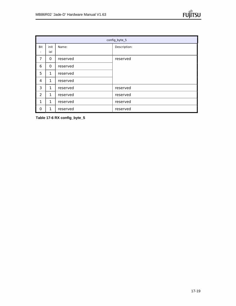
17-19
MB86R02 ‘Jade-D’ Hardware Manual V1.63
config_byte_5
Bit
:
init
ial
Name: Description:
7 0 reserved reserved
6 0 reserved
5 1 reserved
4 1 reserved
3 1 reserved reserved
2 1 reserved reserved
1 1 reserved reserved
0 1 reserved reserved
Table 17-6 RX config_byte_5
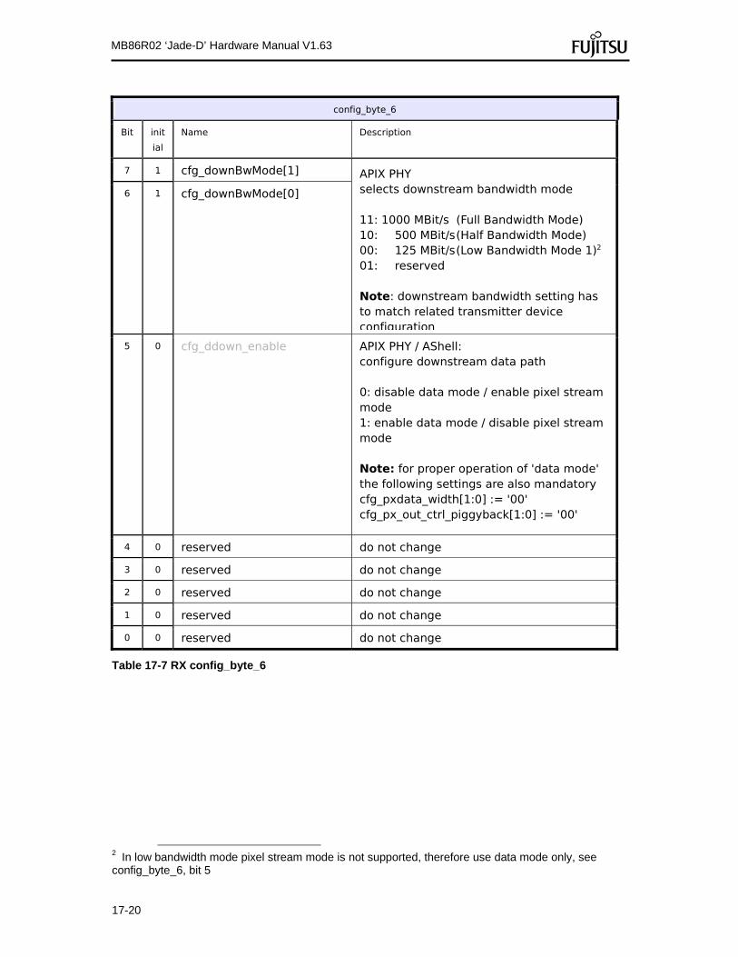
17-20
MB86R02 ‘Jade-D’ Hardware Manual V1.63
config_byte_6
Bit init
ial
Name Description
7 1 cfg_downBwMode[1] APIX PHY selects downstream bandwidth mode 11: 1000 MBit/s (Full Bandwidth Mode) 10: 500 MBit/s (Half Bandwidth Mode) 00: 125 MBit/s (Low Bandwidth Mode 1)2 01: reserved Note: downstream bandwidth setting has to match related transmitter device configuration
6 1 cfg_downBwMode[0]
5 0 cfg_ddown_enable APIX PHY / AShell: configure downstream data path 0: disable data mode / enable pixel stream mode 1: enable data mode / disable pixel stream mode Note: for proper operation of 'data mode' the following settings are also mandatory cfg_pxdata_width[1:0] := '00' cfg_px_out_ctrl_piggyback[1:0] := '00'
4 0 reserved do not change
3 0 reserved do not change
2 0 reserved do not change
1 0 reserved do not change
0 0 reserved do not change
Table 17-7 RX config_byte_6
2 In low bandwidth mode pixel stream mode is not supported, therefore use data mode only, see config_byte_6, bit 5

17-21
MB86R02 ‘Jade-D’ Hardware Manual V1.63
config_byte_7
Bit init
ial
Name Description
7 1 reserved do not change
6 0 reserved
5 0 reserved
4 1 reserved
3 0 reserved do not change
2 0 reserved do not change
1 1 cfg_clk_core1_enable APIX PHY (digital) 1: enable core clock of APIX PHY 0: disable
0 1 cfg_clk_core2_enable APIX PHY (digital) 1: enable core clock of AShell 0: disable
Table 17-8 RX config_byte_7
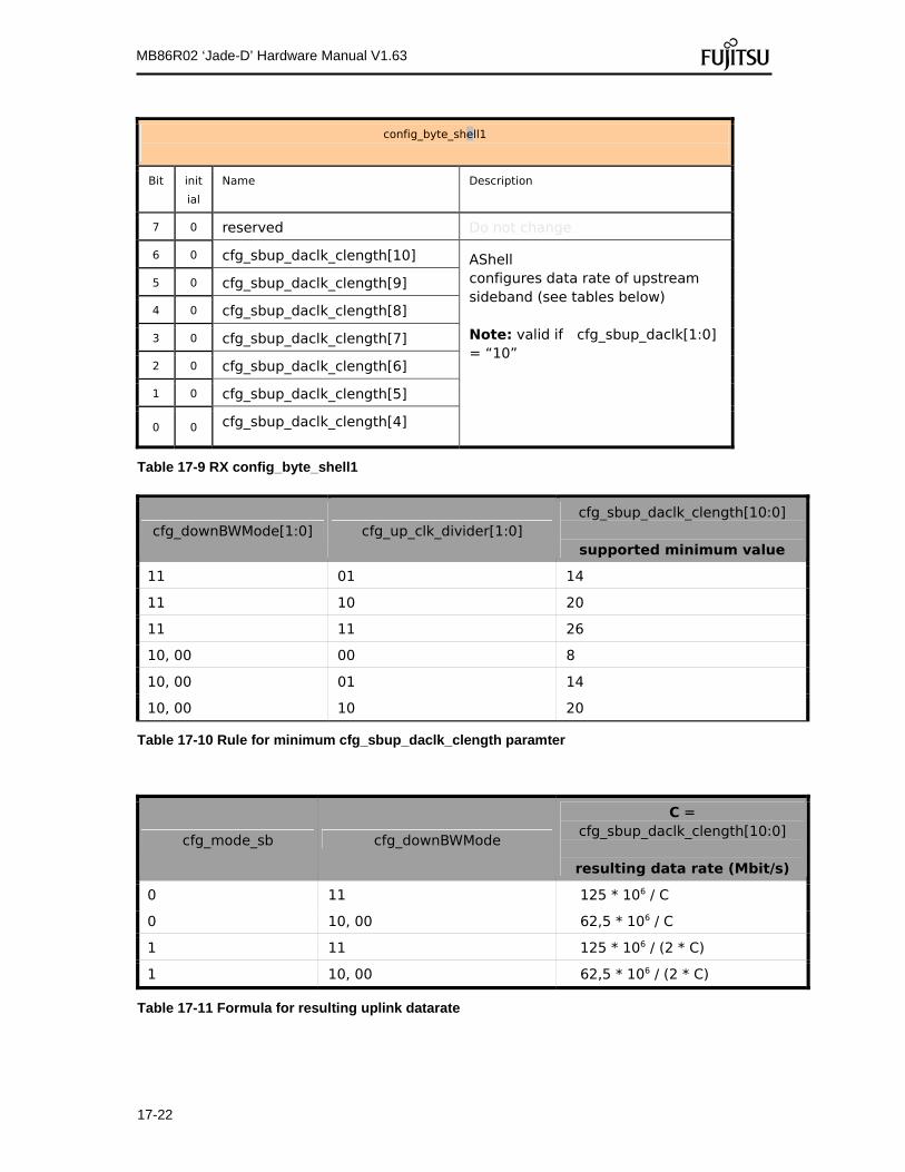
17-22
MB86R02 ‘Jade-D’ Hardware Manual V1.63
config_byte_shell1
Bit init
ial
Name Description
7 0 reserved Do not change
6 0 cfg_sbup_daclk_clength[10] AShell configures data rate of upstream sideband (see tables below) Note: valid if cfg_sbup_daclk[1:0] = “10”
5 0 cfg_sbup_daclk_clength[9]
4 0 cfg_sbup_daclk_clength[8]
3 0 cfg_sbup_daclk_clength[7]
2 0 cfg_sbup_daclk_clength[6]
1 0 cfg_sbup_daclk_clength[5]
0 0 cfg_sbup_daclk_clength[4]
Table 17-9 RX config_byte_shell1
cfg_downBWMode[1:0] cfg_up_clk_divider[1:0] cfg_sbup_daclk_clength[10:0]
supported minimum value
11 01 14
11 10 20
11 11 26
10, 00 00 8
10, 00 01 14
10, 00 10 20
Table 17-10 Rule for minimum cfg_sbup_daclk_clength paramter
cfg_mode_sb cfg_downBWMode
C = cfg_sbup_daclk_clength[10:0]
resulting data rate (Mbit/s)
0 11 125 * 106 / C
0 10, 00 62,5 * 106 / C
1 11 125 * 106 / (2 * C)
1 10, 00 62,5 * 106 / (2 * C)
Table 17-11 Formula for resulting uplink datarate

17-23
MB86R02 ‘Jade-D’ Hardware Manual V1.63
config_byte_shell2
Bit init
ial
Name Description
7 1 cfg_sbup_daclk_clength[3] AShell configures data rate Note: valid if cfg_sbup_daclk[1:0] = “10”
6 0 cfg_sbup_daclk_clength[2]
5 0 cfg_sbup_daclk_clength[1]
4 0 cfg_sbup_daclk_clength[0]
3 1 cfg_sbup_dwidth AShell enable sbup ports 1: sbup_data[1:0] 0: sbup_data[0]
2 0 cfg_sbup_daclk[1] AShell: generate sbup clock and transmit as sbup_data[1] 11: disable 10: with use of internal counter (asynchronous to core_clk of APIX PHY) 01: reserved 00: disable
1 0 cfg_sbup_daclk[0]
0 1 cfg_sbdown_dwidth AShell enable sbdown ports 1: sbdown_data[1:0] 0: sbdown_data[0]
Table 17-12 RX config_byte_shell2

17-24
MB86R02 ‘Jade-D’ Hardware Manual V1.63
config_byte_shell3
Bit init
ial
Name Description
7 0 cfg_sbdown_daclk AShell: validate sbdown_data with 1: sbdown_data[1], 0: internal signal (sbdown_valid)
6 0 Reserved, cfg_ephy AShell: connect internal AShell to external APIX PHY (INAP125R24) through GPIO interface 1: enable 0: disable
5 0 Reserved, cfg_eshell AShell: connect internal APIX PHY to external Ashell through GPIO interface. To use this mode 'cfg_ephy' enable is required. 1: enable 0: disable
4 0 cfg_mode_sb AShell: selects between two different sideband transmission modes 0: mode 0 (toggle mode), see Figure 17-28 , 1: mode 1, see Figure 17-29
3 1 cfg_crc_timeout_value [3] AShell: CRC timeout error is generated after N consecutively received and corrupted transitions (CRC mismatch) N = factor1 * factor2 factor1 = cfg_crc_timeout_value [3:2] factor2 = cfg_crc_timeout_value [1:0] factor 1 factor 2 00: 1 00: 2 01: 4 01: 4 10: 16 10: 6 11: 128 11: 10 example: 1001 N = 64 (16*4) Note: to achieve optimum system behaviour, please adapt to bit fault characteristics of serial link
2 0 cfg_crc_timeout_value [2]
1 0 cfg_crc_timeout_value [1]
0 1 cfg_crc_timeout_value [0]
Table 17-13 RX config_byte_shell3

17-25
MB86R02 ‘Jade-D’ Hardware Manual V1.63
config_byte_shell4
Bit init
ial
Name Description
7 1 cfg_window_size[3] Defines the window size of the acknowledge protocol (supported size: 1...12)
6 0 cfg_window_size[2]
5 1 cfg_window_size[1]
4 0 cfg_window_size[0]
3 0 cfg_arq_off AShell: disable automatic repetition request (ARQ)
1: ARQ disabled 0: ARQ enabled
2 0 cfg_suppress_ita AShell: outbound idle transactions are not sent
1: enable 0: disable
1 0 reserved
0 0 reserved
Table 17-14 RX config_byte_shell4

17-26
MB86R02 ‘Jade-D’ Hardware Manual V1.63
17.4.2 TX
config_byte_1
Bit init
ial
Name Description
7 1 reserved do not change
6 1 reserved do not change
5 1 reserved do not change
4 1 reserved do not change
3 0 reserved do not change
2 0 reserved do not change
1 0 reserved do not change
0 0 reserved do not change
Table 17-15 TX config_byte_1

17-27
MB86R02 ‘Jade-D’ Hardware Manual V1.63
config_byte_2
Bit
:
init
ial
Name Description
7 1 cfg_dwnBwMode[1] APIX PHY (Hard IP): selects downstream bandwidth mode 11: 1000 Mbit/s (Full Bandwidth Mode) 10: 500 Mbit/s (Half Bandwidth Mode) 01: 250 Mbit/s (Low Bandwidth Mode 2) 00: 125 Mbit/s (Low Bandwidth Mode 1)
6 1 cfg_dwnBwMode[0]
5 1 Reserved Do not change
4 1 Reserved Do not change
3 1 cfg_px_in_ctrl_piggyback[1] APIX PHY (Soft IP): transmission of pixel controls 00: never 01: unused 10: with even pixels only 11: with every pixel
2 1
cfg_px_in_ctrl_piggyback[0]
1 1 cfg_pxdata_width[1] APIX PHY (Soft IP): bit width of pixel data 00: 10 bits 01: 12 bits 10: 18 bits 11: 24 bits
0 0 cfg_pxdata_width[0]
Table 17-16 TX config_byte_2 The maximum pixel clock frequencies listed in Table 17-1 are achievable only if pixel controls are transmitted with even pixels ('cfg_px_in_ctrl_piggyback' = "10").
pixel data bit width
maximum pixel clock frequency using Full Bandwidth (1 GBit/s) Mode
maximum pixel clock frequency using
Half Bandwidth (500 MBit/s) Mode
10 62.0 MHz 31.0 MHz
12 61.0 MHz 30.5 MHz
18 42.0 MHz 21.0 MHz
24 32.0 MHz 16.0 MHz
Table 17-1, maximum pixel clock frequency with cfg_px_in_ctrl_piggyback[1:0] = “10”

17-28
MB86R02 ‘Jade-D’ Hardware Manual V1.63
config_byte_3
Bit
:
init
ial
Name Description
7 0 reserved do not change
6 0 cfg_upBwMode[1] APIX PHY (Hard IP): upstream bandwidth mode configuration 00: 62.503 Mbit/s(Full, Half, Low Bandwidth Mode) 01: 41.67 Mbit/s(Full Bandwidth Mode) 11: 20.83 Mbit/s(Half and Low Bandwidth Mode) 10: 31.25 Mbit/s(Full, Half, Low Bandwidth Mode)
5 0 cfg_upBwMode[0]
4 0 reserved Do not change
3 0 cfg_upSmpOfst[3] APIX PHY (Hard IP): upstream sampling point configuration 0000: optimum sampling point when operating in 62.50 Mbit/s mode 0010: optimum sampling point when operating in 41.67 Mbit/s or 31.25 Mbit/s mode 0100: optimum sampling point when operating in 20.83 Mbit/s mode
2 0 cfg_upSmpOfst[2]
1 0 cfg_upSmpOfst[1]
0 0 cfg_upSmpOfst[0]
Table 17-17 TX config_byte_3
config_byte_4
Bit
:
init
ial
Name Description
7 1 reserved do not change
6 0 reserved do not change
5 0 reserved do not change
4 1 reserved do not change
3 0 reserved do not change
2 0 reserved do not change
1 0 reserved do not change
0 1 reserved do not change
Table 17-18 TX config_byte_4
3 If a setup with the external AShell is used and the external AShell is running with a 62.5 MHz core clock, then the 62.5MBit/s upstream channel bandwidth for half and low bandwidth mode is not supported.

17-29
MB86R02 ‘Jade-D’ Hardware Manual V1.63
config_byte_5
Bit
:
init
ial
Name Description
7 0
cfg_ddown_enable APIX PHY (Soft IP) / Ashell: configure downstream data path 0: disable data mode / enable pixel stream mode 1: enable data mode / disable pixel stream mode Note: for proper operation the following settings are mandatory cfg_pxdata_width[1:0] := '00' cfg_px_in_ctrl_piggyback[1:0] := '00'
6 0
cfg_sbdown_smode APIX PHY (Soft IP): relation of downstream sideband data to core clock of APIX PHY 0: asynchronous (sb data are 2-stage registered internal, have to be used with external AShell) 1: synchronous (have to be used with internal AShell)
5 1 cfg_clk_core1_enable APIX PHY (Soft IP)
1: enable core clock of APIX PHY 0: disable
4 0 cfg_clk_core2_enable APIX PHY (Soft IP)
1: enable core clock of Ashell 0: disable
3 0 reserved do not change
2 1 reserved do not change
1 0 reserved do not change
0 0 reserved do not change
Table 17-2 TX Config_byte_5
config_byte_6
Bit init
ial
Name Description
7 0 reserved do not change
6 0 reserved do not change

17-30
MB86R02 ‘Jade-D’ Hardware Manual V1.63
5 1 reserved do not change
4 1 reserved do not change
3 0 reserved do not change
2 0 reserved do not change
1 1 reserved do not change
0 1 reserved do not change
Table 17-19 TX config_byte_6

17-31
MB86R02 ‘Jade-D’ Hardware Manual V1.63
config_byte_7
Bit init
ial
Name Description
7 1 reserved do not change
6 1 reserved
5 0 reserved
4 0 reserved
3 0 reserved do not change
2 1 reserved do not change
1 1 reserved do not change
0 1 reserved do not change
Table 17-20 TX config_byte_7
config_byte_8
Bit init
ial
Name Description
7 0 cfg_trigger_cycle_length[6] APIX PHY (Soft IP): configures cycle length of 'sbdown_trigger's pulse pattern 9 : required when operating in Full and Half Bandwidth Mode 18 : required when operating in Low Bandwidth Mode 2 (APIX PHY core_clk == 62.5 MHz) 36 : required when operating in Low Bandwidth Mode 1 (APIX PHY core_clk == 62.5 MHz) 36 : required when operating in Low Bandwidth Mode 2 (APIX PHY core_clk == 125 MHz) 72 : required when operating in Low Bandwidth Mode 1 (APIX PHY core_clk == 125 MHz)
6 0 cfg_trigger_cycle_length[5]
5 0 cfg_trigger_cycle_length[4]
4 1 cfg_trigger_cycle_length[3]
3 0 cfg_trigger_cycle_length[2]
2 0 cfg_trigger_cycle_length[1]
1 1
cfg_trigger_cycle_length[0]
0 0 reserved do not change
Table 17-3 TX config_byte_8

17-32
MB86R02 ‘Jade-D’ Hardware Manual V1.63
config_byte_9
Bit init
ial
Name Description
7 0 cfg_trigger_active_length[6] APIX PHY (Soft IP): configures high pulse width of signal 'sbdown_trigger' (multiples of core clk cycle) 0: 1 cycle 1: 2 cycles (default) 2: 3 cycles ... 71: 72 cycles
6 0 cfg_trigger_active_length[5]
5 0 cfg_trigger_active_length[4]
4 0 cfg_trigger_active_length[3]
3 0 cfg_trigger_active_length[2]
2 0 cfg_trigger_active_length[1]
1 1 cfg_trigger_active_length[0]
0 0 reserved do not change
Table 17-4 TX config_byte_9
config_byte_10
Bit init
ial
Name Description
7 0 cfg_trigger_offset[6] APIX PHY (Soft IP): configure start position of signal 'sbdown_trigger' (multiples of core clk cycle relative to “strobe position”) 0: 0 cycles (“strobe”) 1: 1 cycle (“request”) 1: 2 cycles ... 71: 71 cycles
6 0 cfg_trigger_offset[5]
5 0 cfg_trigger_offset[4]
4 0 cfg_trigger_offset[3]
3 0 cfg_trigger_offset[2]
2 0 cfg_trigger_offset[1]
1 1 cfg_trigger_offset[0]
0 0 reserved do not change
Table 17-5 TX config_byte_10

17-33
MB86R02 ‘Jade-D’ Hardware Manual V1.63
config_byte_11
Bit init
ial
Name Description
7 0 cfg_sbup_valid_active_length[1] APIX PHY (Soft IP): configure high pulse width of signal 'sbup_valid' (multiples of core clk cycle) 11: 4 cycles 10: 3 cycles 01: 2 cycles 00: 1 cycle
6 1
cfg_sbup_valid_active_length[0]
5 0 reserved do not change
4 0 reserved do not change
3 0 reserved do not change
2 0 reserved do not change
1 0 reserved do not change
0 0 reserved do not change
Table 17-21 TX config_byte_11

17-34
MB86R02 ‘Jade-D’ Hardware Manual V1.63
config_byte_shell1
Bit init
ial
Name Description
7 0
cfg_sbdown_clk AShell: functional meaning of 'sbdown_trigger' when 'cfg_trigger_offset' is set to 0 0: request 1: strobe (only use with internal APIX PHY)
6 0 cfg_sbdown_daclk_clength[6] AShell configures data rate of downstream sideband (see tables below) Note: valid if cfg_sbup_daclk[1:0] = “10” AShell: configures cycle time of sbdown clock (multiples of Ashell core clock) when sbdown_data are asynchronous (sbdown_data[1] is used as sbdown clock) or cfg_mode_sb is enabled (mode1) 11:recommended minimum (no low bandwidth mode, AShell and APIX PHY operate at same core clock frequency) 20:recommended minimum (low bandwidth mode 2, AShell and APIX PHY operate at 62.5 MHz)
5 1 cfg_sbdown_daclk_clength[5]
4 0 cfg_sbdown_daclk_clength[4]
3 0 cfg_sbdown_daclk_clength[3]
2 1 cfg_sbdown_daclk_clength[2]
1 1 cfg_sbdown_daclk_clength[1]
0 0
cfg_sbdown_daclk_clength[0]
Table 17-22 TX config_byte_shell1
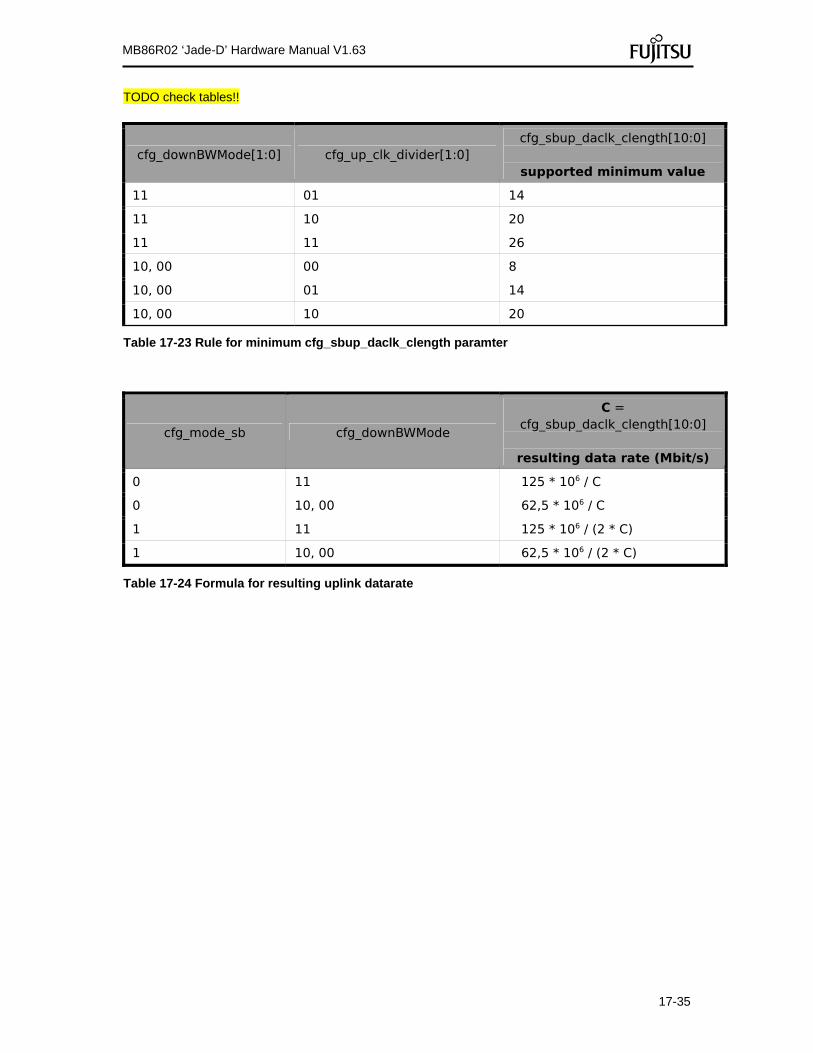
17-35
MB86R02 ‘Jade-D’ Hardware Manual V1.63
TODO check tables!!
cfg_downBWMode[1:0] cfg_up_clk_divider[1:0] cfg_sbup_daclk_clength[10:0]
supported minimum value
11 01 14
11 10 20
11 11 26
10, 00 00 8
10, 00 01 14
10, 00 10 20
Table 17-23 Rule for minimum cfg_sbup_daclk_clength paramter
cfg_mode_sb cfg_downBWMode
C = cfg_sbup_daclk_clength[10:0]
resulting data rate (Mbit/s)
0 11 125 * 106 / C
0 10, 00 62,5 * 106 / C
1 11 125 * 106 / (2 * C)
1 10, 00 62,5 * 106 / (2 * C)
Table 17-24 Formula for resulting uplink datarate

17-36
MB86R02 ‘Jade-D’ Hardware Manual V1.63
config_byte_shell2
Bit init
ial
Name Description
7 1 cfg_sbup_dwidth AShell: enable sbup ports 1: sbup_data[1:0] 0: sbup_data[0]
6 0 cfg_sbup_daclk AShell: validate sbup_data with 1: sbup_data[1] 0: sbup_valid
5 1 cfg_sbdown_dwidth AShell: enable sbdown ports 1: sbdown_data[1:0] 0: sbdown_data[0]
4 0 cfg_sbdown_daclk[1] AShell: generate sbdown clock and transmit as sbdown_data[1] 11: disable 10: with use of internal counter (asynchronous to core_clk of APIX PHY) 01: with use of sbdown_trigger (synchronous to core_clk of APIX PHY) 00: disable
3 0 cfg_sbdown_daclk[0]
2 0 cfg_ephy AShell: connect internal Ashell to external APIX PHY through GPIO interface 1: enable 0: disable
1 1 cfg_eshell AShell: connect internal APIX PHY to external AShell through GPIO interface 1: enable 0: disable
0 0 cfg_mode_sb AShell: selects between two different sideband transmission modes 0: mode0: see Figure 17-28 Mode 0 ) 1: mode1: see Figure 17-29 Mode bandwidth has to be set with cfg_sbdown_daclk_clength
Table 17-25 TX config_byte_shell2

17-37
MB86R02 ‘Jade-D’ Hardware Manual V1.63
config_byte_shell3
Bit init
ial
Name Description
7 1 cfg_crc_timeout_value [3] AShell: CRC timeout error is generated after N consecutive CRC errors (format: base x multiplier) example: 1011 = 16*10 = 160 multiplier [3:2] base [1:0] 00: 1 00: 2 01: 4 01: 4 10: 16 10: 6 11: 128 11: 10
6 0 cfg_crc_timeout_value [2]
5 0 cfg_crc_timeout_value [1]
4 1 cfg_crc_timeout_value [0]
3 1 cfg_window_size[3] AShell: defines the window size of the acknowledge protocol (supported size: 1...12)
2 0 cfg_window_size[2]
1 1 cfg_window_size[1]
0 0 cfg_window_size[0]
Table 17-26 TX config_byte_shell3
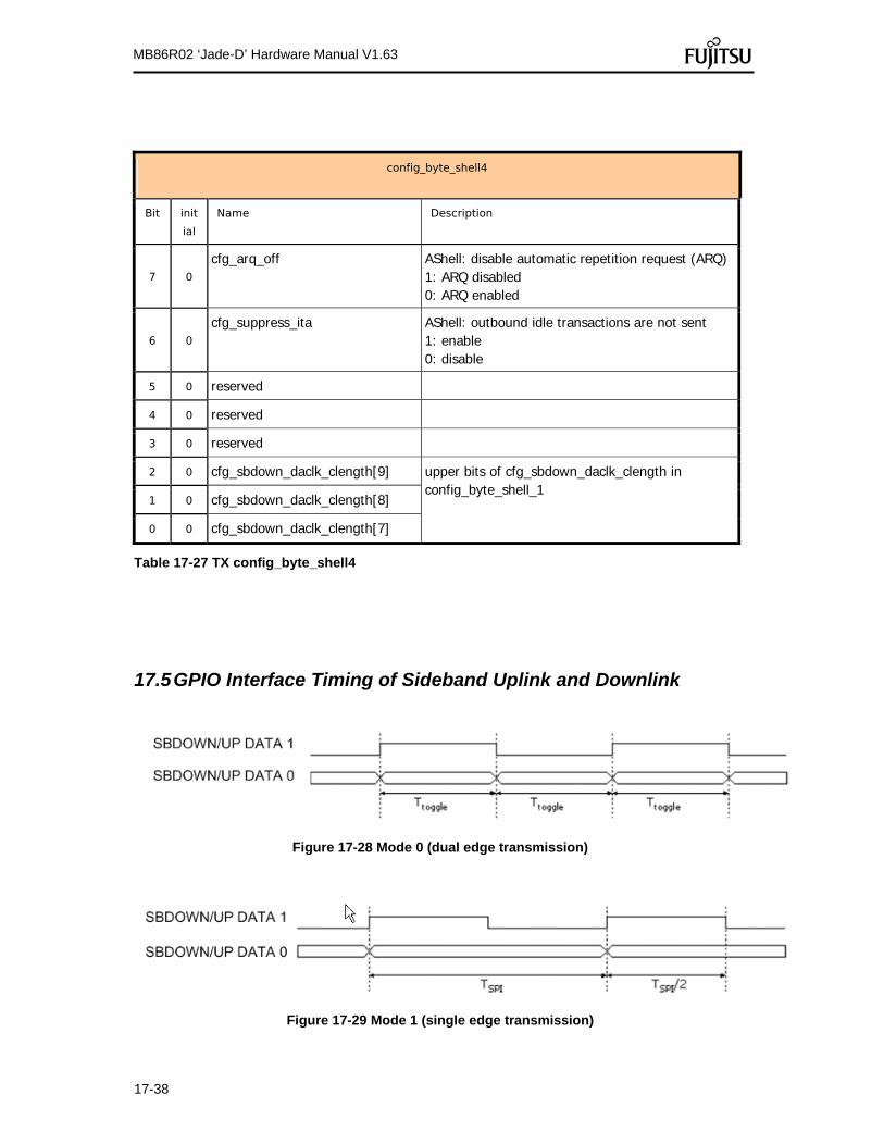
17-38
MB86R02 ‘Jade-D’ Hardware Manual V1.63
config_byte_shell4
Bit init
ial
Name Description
7 0 cfg_arq_off AShell: disable automatic repetition request (ARQ)
1: ARQ disabled 0: ARQ enabled
6 0 cfg_suppress_ita AShell: outbound idle transactions are not sent
1: enable 0: disable
5 0 reserved
4 0 reserved
3 0 reserved
2 0 cfg_sbdown_daclk_clength[9] upper bits of cfg_sbdown_daclk_clength in config_byte_shell_1
1 0 cfg_sbdown_daclk_clength[8]
0 0 cfg_sbdown_daclk_clength[7]
Table 17-27 TX config_byte_shell4
17.5 GPIO Interface Timing of Sideband Uplink and Downlink
Figure 17-28 Mode 0 (dual edge transmission)
Figure 17-29 Mode 1 (single edge transmission)

17-39
MB86R02 ‘Jade-D’ Hardware Manual V1.63
17.6 Control Flow
//Global APIX PHY and PLL config set APPLLCFG.En_PLL = 1; // Enable PLL set COMPHYCFG.En_OffsetComp = 1; // Enable Offset Compensation //config of channel n=0 of used Ashell, here e.g. TX Ashell Tn set CHnCFG.ENUpPHY = 1; set CHnCFG.ENDwnPHY = 1 // Enable upstream/downstream PHY // deactivate resets Set APPLLCFG.PhyPllReset = 0; // PLL reset deactivate Set COMPHYCFG.SwRstToPHY; // APIX PHY reset deactivate set TnCTRL.CFGEN = 1 set TnCFG0 = xx set TnCFG1 = xx set TnCFG2 = xx set TnCTRL.CFGEN = 0 read TnSTS0 (check for TnPHYUPREADY ==1, TnPLLGOOD ==1) provide valid pixeldata RGB , HS,VS ,DE read @Indigo RH ASStatus (check for rx_px_aligned) same for channel n = 1

17-40
MB86R02 ‘Jade-D’ Hardware Manual V1.63
17.6.1 Use cases
17.6.1.1 Use case 1
Feedthrough of 2bit sideband data MCU467S Ashell Jade-D APIX PHY TX Indigo APIX PHY RX & Ashell 2bit Sideband Datawidth
Figure 17-30 Use Case 1
Jade-D MCU467S
pin name direction pin name direction function
APIXn_SB_0 in TDAn0 out Sideband GPIO Data bit 0
downAPIXn_SB_1 in TDAn1 out
Sideband GPIO Data bit 1
APIXn_SB_2 out TCKIn in Sideband Clock
APIXn_SB_3 out RDAn0 in Sideband GPIO Data bit 0
up APIXn_SB_4 out RDAn1 in
Sideband GPIO Data bit 1
APIXn_SB_5 out RCKn in Sideband Clock
Table 17-6 Use Case 1 n = channel number = 0..1
17.6.1.1.1 Jade-D configuration
Table 17-7, Jade-D APIX TX configuration vectors for use case 1
Jade-D configuration config_byte_1 F0h config_byte_2 FEh config_byte_3 00h

17-41
MB86R02 ‘Jade-D’ Hardware Manual V1.63
config_byte_4 91h config_byte_5 24h config_byte_6 33h config_byte_7 C7h config_byte_8 12h config_byte_9 02h config_byte_10 02h config_byte_11 40h config_byte_shell_1 26h config_byte_shell_2 A2h config_byte_shell_3 9Ah config_byte_shell_4 00h
17.6.1.1.2 MB91F467SA configuration
Table 17-8, MB91F467SA APIX TX configuration vectors for use case 1
MCU467S configuration config_byte_1 00h config_byte_2 30h config_byte_3 00h config_byte_4 90h config_byte_5 50h config_byte_6 00h config_byte_7 00h config_byte_8 48h config_byte_9 02h config_byte_10 02h config_byte_11 40h config_byte_shell_1 26h config_byte_shell_2 A4h config_byte_shell_3 9Ah config_byte_shell_4 00h ANALOG PARAMETERS are subject to change
17.6.1.1.3 Indigo configuration
Use Indigo Modepins APIX_CFG[2:0]=111
Indigo configuration config_byte_1 7Fh config_byte_2 BCh config_byte_3 86h config_byte_4 00h

17-42
MB86R02 ‘Jade-D’ Hardware Manual V1.63
config_byte_5 61h config_byte_6 C0h config_byte_7 93h config_byte_shell_1 00h config_byte_shell_2 E9h config_byte_shell_3 09h config_byte_shell_4 A0h ANALOG PARAMETERS are subject to change
Table 17-9, Indigo Configuration
17.6.1.2 Use case 2
Feedthrough of 1bit sideband data MCU467S Ashell Jade-D APIX PHY TX Indigo APIX PHY RX & Ashell 1bit Sideband Datawidth
Figure 17-31 Use Case 2
Jade-D MCU467S
pin name direction pin name direction function
APIXn_SB_0 in TDAn0 out Sideband GPIO Data bit 0
downAPIXn_SB_1 unused
APIXn_SB_2 out TCKIn in Sideband Clock
APIXn_SB_3 out RDAn0 in Sideband GPIO Data bit 0
up APIXn_SB_4 unused APIXn_SB_5 out RCKn in Sideband Clock
Table 17-10 Use Case 2

17-43
MB86R02 ‘Jade-D’ Hardware Manual V1.63
17.6.1.2.1 Jade-D configuration
Table 17-11, Jade-D APIX TX configuration vectors for use case 2
Jade-D configuration config_byte_1 00h config_byte_2 FEh config_byte_3 00h config_byte_4 91h config_byte_5 24h config_byte_6 33h config_byte_7 C7h config_byte_8 12h config_byte_9 02h config_byte_10 02h config_byte_11 40h config_byte_shell_1 26h config_byte_shell_2 02h config_byte_shell_3 9Ah config_byte_shell_4 00h
Configuration
Vector:
config_byte_shell_2
Bit: Default: Name: Description:
7 0 cfg_sbup_dwidth AShell: enable sbup ports 1: sbup_data[1:0] 0: sbup_data[0]
5 0
cfg_sbdown_dwidth AShell: enable sbdown ports 1: sbdown_data[1:0] 0: sbdown_data[0]
All other parameters are default reset values.
17.6.1.2.2 MB91F467SA configuration
Table 17-12, MB91F467SA APIX TX configuration vectors for use case 1
MCU467S configuration config_byte_1 00h config_byte_2 30h config_byte_3 00h config_byte_4 90h config_byte_5 50h config_byte_6 00h
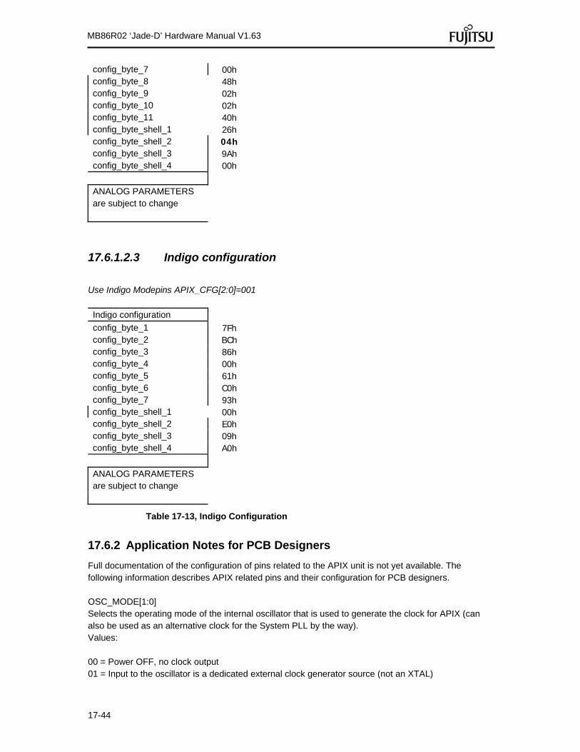
17-44
MB86R02 ‘Jade-D’ Hardware Manual V1.63
config_byte_7 00h config_byte_8 48h config_byte_9 02h config_byte_10 02h config_byte_11 40h config_byte_shell_1 26h config_byte_shell_2 04h config_byte_shell_3 9Ah config_byte_shell_4 00h ANALOG PARAMETERS are subject to change
17.6.1.2.3 Indigo configuration
Use Indigo Modepins APIX_CFG[2:0]=001
Indigo configuration config_byte_1 7Fh config_byte_2 BCh config_byte_3 86h config_byte_4 00h config_byte_5 61h config_byte_6 C0h config_byte_7 93h config_byte_shell_1 00h config_byte_shell_2 E0h config_byte_shell_3 09h config_byte_shell_4 A0h ANALOG PARAMETERS are subject to change
Table 17-13, Indigo Configuration
17.6.2 Application Notes for PCB Designers
Full documentation of the configuration of pins related to the APIX unit is not yet available. The following information describes APIX related pins and their configuration for PCB designers. OSC_MODE[1:0] Selects the operating mode of the internal oscillator that is used to generate the clock for APIX (can also be used as an alternative clock for the System PLL by the way). Values: 00 = Power OFF, no clock output 01 = Input to the oscillator is a dedicated external clock generator source (not an XTAL)

17-45
MB86R02 ‘Jade-D’ Hardware Manual V1.63
10 = Input to the oscillator is an external XTAL which uses an internal feedback resistor 11 = Input to the oscillator is an external XTAL which uses an external feedback resistor OSC_BIAS[1:0] Sets the internal oscillator's bias level for 4 configurable settings which provide a compromise between clock jitter and current consumption: 00 = Highest clock jitter, lowest current consumption 01 = High clock jitter, lower current consumption 10 = Low clock jitter, high current consumption 11 = Lowest clock jitter, highest current consumption Note: Until the chip has been validated and real life values measured, it is not possible to make a fixed recommendation for a specific application. However, until then, setting 11 makes the most sense (best clock characteristics, but higher current consumption). OSC_FILTER Sets the characteristics of an internal low-pass post-oscillator filter. This filter is integrated in order to improve the robustness of the internal circuit to external RF interference signals. The cut-off frequency of this filter is programmable to allow a clock of either 62.5 MHz or 20 MHz. OSCFilter should not be changed when the clock from the oscillator is being used and it is therefore implemented as an external pin for setup. The setting that should be used depends on the clock frequency: 0 = max. clock of 62.5 MHz 1 = max. clock of 20 MHz

18-1
MB86R02 ‘Jade-D’ Hardware Manual V1.63
18 Graphics Display Controller (GDC)
18.1 Preface
The embedded graphics core implemented in the MB86R02 'Jade-D' contains two display controllers which are upwards compatible to the MB86296 (Coral PA) GDC.
18.2 Features
Display controllers
The MB86R02 'Jade-D' has two display controllers that are compatible with the Coral PA.
This GDC supports XGA (1024 768 pixels) display, 6-layer overlay, left/right split display, wrap-around scrolling, double buffers and translucent display.
Digital video capture
The MB86R02 'Jade-D' has two video capture units that are compatible with the Coral PA.
The digital video capture units can store digital video data such as TV in graphics memory and display drawn images and video images on the same screen.
Geometry Engine
The Geometry Engine executes geometry processing and is basically compatible with Coral PA. Display lists created for Coral series (MB86293 - MB86296) GDCs can be drawn. When intensive geometric operations processing such as coordinate conversions or clipping are performed by this GDC, the workload of a CPU can be dramatically reduced.
2D and 3D Drawing
The drawing functionality of MB86R02 'Jade-D' is compatible to that of the Coral PA . It can draw data using display lists created for Coral series GDCs(MB86293 - MB86296).
The MB86R02 'Jade-D' also supports 3D rendering, such as texture mapping with perspective collection and Gouraud shading, alpha blending and anti-aliasing for drawing smooth lines.
Endian
Little endian is supported by the Jade-D GDC in the same way as for Coral PA.
For 32 bit access, both Little endian and Big endian access are handled using the same byte ordering in the GDC.

18-2
MB86R02 ‘Jade-D’ Hardware Manual V1.63
18.3 Functional Overview
18.3.1 Display controller
Video data output
Dual digital video outputs are provided.
Screen resolution
LCD panels with wide range of resolutions are supported by using a programmable timing generator as follows:
Screen Resolutions
Resolutions 1024 768 1024 600 800 600 854 480 640 480 480 234 400 234 320 234
Hardware cursor
MB86R02 'Jade-D' supports two hardware cursor functions. Each of these hardware cursors is specified as a 64 64-pixel area. Each pixel of these hardware cursors is 8 bits and uses the same look-up table as indirect color mode.
Double buffer method
Double buffer method in which drawing window and display window is switched in units of 1 frame enables the smooth animation.
Flipping (switching of display window area) is performed in synchronization with the vertical blanking period using program.
Scroll method
Independent setting of drawing and display windows and their starting positions makes smooth scrolling possible.
Display colors
Supports indirect color mode which uses the look-up table (color palette) in 8 bits/pixels.
An entry in the look-up table (color palette) has 8 bits, in other words 256 entries are possible. The color data itself is saved as 6 bits of RGB data. Consequently, 256 colors can be displayed out of 260,000 possible colors.
Supports direct color mode which specifies RGB with 16 bits/pixel.
Supports direct color mode which specifies RGB with 24 bits/pixel.

18-3
MB86R02 ‘Jade-D’ Hardware Manual V1.63
Overlay
Compatibility mode
Up to four extra layers (C, W, M and B) can be displayed overlaid.
The overlay position for the hardware cursors is above/below the top layer (C).
The transparent mode or the blend mode can be selected for overlay.
The M and B-layers can be split into separate windows.
Window display can be performed for the W-layer.
Two palettes are provided: C-layer and M-/B-layer.
The W-layer is used as the video input layer.
Window mode
Up to six screens (L0 to 5) can be displayed overlaid.
The overlay sequence of the L0- to L5-layers can be changed arbitrarily.
The overlay position for the hardware cursors is above/below the L0-layer.
The transparent mode or the blend mode can be selected for overlay.
The L5 layer can be used as the blend coefficient plane (8 bits/pixel).
Window display can be performed for all layers.
Four palettes corresponding to L0 to L3 are provided.
The L1 layer is used as the video input layer.
Background color display is supported in window display for all layers.
L0, L2, L4 (0,0) L3, L5 (HDB1, 0)L1 (WX, WY)
L0 (L0WX, L0WY) L2 (L2WX, L2WY)
L1 (L1WX, L1WY)L5 (L5WX, L5WY)
L4 (L4WX, L4WY)
L3 (L3WX, L3WY)

18-4
MB86R02 ‘Jade-D’ Hardware Manual V1.63
18.3.2 Video capture function
Video input
This device has two video input ports
One video input port supports both ITU RBT-656 and RGB666, the other supports RGB666 only
Video data is stored in graphics memory and later displayed on the screen in synchronization with the display scan
Scaling
A upscale factor of 1 to 2 can be used. PAL or NTSC images can be displayed on a wide screen
A downscale factor of 1 to 1/32 can be used
Picture-in-picture can be used to display drawn images and video images on the same screen
18.3.3 Geometry processing
The MB86R02 'Jade-D' has a geometry engine for performing the numerical operations required for intensive graphics processing. The geometry engine uses the floating-point format for highly precise operations. It selects the required geometry processing according to the configured drawing mode and primitive type and executes processing for the final drawing.
Primitives
Point, line, line strip, independent triangle, triangle strip, triangle fan and arbitrary polygon are supported.
MVP Transformation
MVP Transformation
A 4 4 transformation matrix enables the transformation of a 3D model view projection. Two-dimensional affine transformation is also possible.
Clipping
Clipping stops the drawing of objects outside the window (field of view). Polygons (including concave shapes) can also be clipped.
Culling
Rear-facing triangles are not drawn.
3D-2D Transformation
These functions transform 3D coordinates (normalization) into 2D coordinates in orthogonal or perspective projections.
View port transformation
This function transforms normalized 2D coordinates into drawing (device) coordinates.
Primitive setup
This function automatically performs a variety of slope computations, etc., based on transforming vertex data into coordinates and prepares for rendering (setup).
Log output of device coordinates
The view port conversion results are output to the local memory.
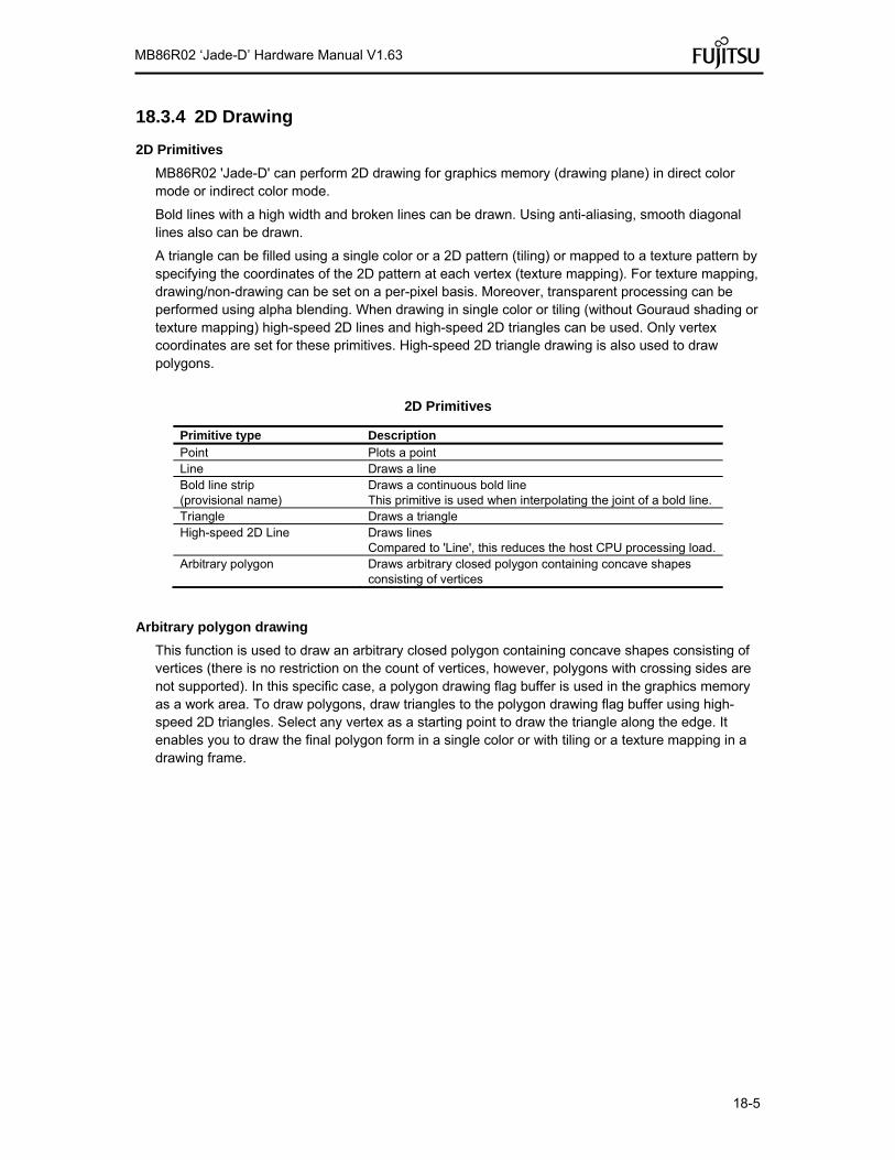
18-5
MB86R02 ‘Jade-D’ Hardware Manual V1.63
18.3.4 2D Drawing
2D Primitives
MB86R02 'Jade-D' can perform 2D drawing for graphics memory (drawing plane) in direct color mode or indirect color mode.
Bold lines with a high width and broken lines can be drawn. Using anti-aliasing, smooth diagonal lines also can be drawn.
A triangle can be filled using a single color or a 2D pattern (tiling) or mapped to a texture pattern by specifying the coordinates of the 2D pattern at each vertex (texture mapping). For texture mapping, drawing/non-drawing can be set on a per-pixel basis. Moreover, transparent processing can be performed using alpha blending. When drawing in single color or tiling (without Gouraud shading or texture mapping) high-speed 2D lines and high-speed 2D triangles can be used. Only vertex coordinates are set for these primitives. High-speed 2D triangle drawing is also used to draw polygons.
2D Primitives
Primitive type Description Point Plots a point Line Draws a line Bold line strip (provisional name)
Draws a continuous bold line This primitive is used when interpolating the joint of a bold line.
Triangle Draws a triangle High-speed 2D Line Draws lines
Compared to 'Line', this reduces the host CPU processing load. Arbitrary polygon Draws arbitrary closed polygon containing concave shapes
consisting of vertices
Arbitrary polygon drawing
This function is used to draw an arbitrary closed polygon containing concave shapes consisting of vertices (there is no restriction on the count of vertices, however, polygons with crossing sides are not supported). In this specific case, a polygon drawing flag buffer is used in the graphics memory as a work area. To draw polygons, draw triangles to the polygon drawing flag buffer using high-speed 2D triangles. Select any vertex as a starting point to draw the triangle along the edge. It enables you to draw the final polygon form in a single color or with tiling or a texture mapping in a drawing frame.
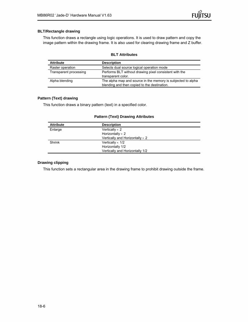
18-6
MB86R02 ‘Jade-D’ Hardware Manual V1.63
BLT/Rectangle drawing
This function draws a rectangle using logic operations. It is used to draw pattern and copy the image pattern within the drawing frame. It is also used for clearing drawing frame and Z buffer.
BLT Attributes
Attribute Description Raster operation Selects dual source logical operation mode Transparent processing Performs BLT without drawing pixel consistent with the
transparent color. Alpha blending The alpha map and source in the memory is subjected to alpha
blending and then copied to the destination.
Pattern (Text) drawing
This function draws a binary pattern (text) in a specified color.
Pattern (Text) Drawing Attributes
Attribute Description Enlarge Vertically 2
Horizontally 2 Vertically and Horizontally 2
Shrink Vertically 1/2 Horizontally 1/2 Vertically and Horizontally 1/2
Drawing clipping
This function sets a rectangular area in the drawing frame to prohibit drawing outside the frame.

18-7
MB86R02 ‘Jade-D’ Hardware Manual V1.63
18.3.5 3D Drawing
3D Primitives
This function draws 3D objects in drawing memory in direct color mode.
3D Primitives
Primitive Description Point Plots 3D point Line Draws 3D line Triangle Draws 3D triangle Arbitrary polygon Draws arbitrary closed polygon containing concave shapes
consisting of vertexes
3D Drawing attributes
Texture mapping with bi-linear filtering/automatic perspective correction and Gouraud shading provides high-quality, realistic 3D drawing. A built-in texture mapping unit performs fast pixel calculations. This unit also delivers color blending between the shading color and texture color.
Hidden plane management
MB86R02 'Jade-D' has a Z buffer for hidden plane management.

18-8
MB86R02 ‘Jade-D’ Hardware Manual V1.63
18.3.6 Special effects
Anti-aliasing
Anti-aliasing manipulates the line borders of polygons in sub-pixel units and blends the pre-drawing pixel color with the background color to make 'jaggies' smooth. It is used as a functional option for 2D drawing (in direct color mode only).
Bold line and broken line drawing
This function draws lines of a specific width and a broken line.
Line Drawing Attributes
Attribute Description Line width Selectable from 1 to 32 pixels Broken line Set by 32 bit or 24 bit of broken line pattern
Supports vertical starting and ending points.
Supports vertical broken line patterns.
Interpolation of bold line joints supports the following modes:
(1) Broken line pattern reference address fix mode
The same broken line pattern is continuously referenced during the period of some pixels starting from the joint and the starting point for the next line.
(2) No interpolation
Supports width equalization of bold lines.
Supports bold line edging.
Does not support anti-aliasing of dashed line patterns.
For a part overlaid due to connection of bold lines, natural overlay can be represented by providing depth information (Z value).
Shading
This GDC supports shading primitives.
Drawing is performed at the body primitive coordinates (X, Y) with a shade as an offset. When drawing, the Z buffer is used in order to differentiate between the body and shade.

18-9
MB86R02 ‘Jade-D’ Hardware Manual V1.63
Alpha blending
Alpha blending blends two image colors to provide a transparent effect. MB86R02 'Jade-D' supports two types of blending; blending two different colors at drawing and blending overlay planes at display. Transparent color is not used for these blending options.
There are two ways of specifying alpha blending for drawing:
(1) Set a transparent coefficient to the register; the transparent coefficient is applied for transparency processing of one plane.
(2) Set a transparent coefficient for each vertex of the plane; as with Gouraud shading, the transparent coefficient is linear-interpolated to perform transparent processing in pixel units.
In addition to the above, the following settings can be performed at texture mapping. When the most significant bit of each texture cell is 1, drawing or transparency can be set. When the most significant bit of each texture cell is 0, non-drawing can be set.
Alpha Blending
Type Description
Drawing Transparent ratio set in particular register
While one primitive (polygon, pattern, etc.), being drawn, registered transparent ratio applied
A transparent coefficient set for each vertex. A linear-interpolated transparent coefficient applied.
This is possible only in direct color mode.
Overlay display Blends top layer pixel color with lower layer pixel color
Transparent coefficient set in particular register
Registered transparent coefficient applied during one frame scan
Gouraud Shading
Gouraud shading can be used in the direct color mode to provide 3D object real shading and color gradation.
Gray Scale Gouraud Shading
Gray scale gouraud shading can be used in the in-direct color mode to draw a blend coefficient layer.
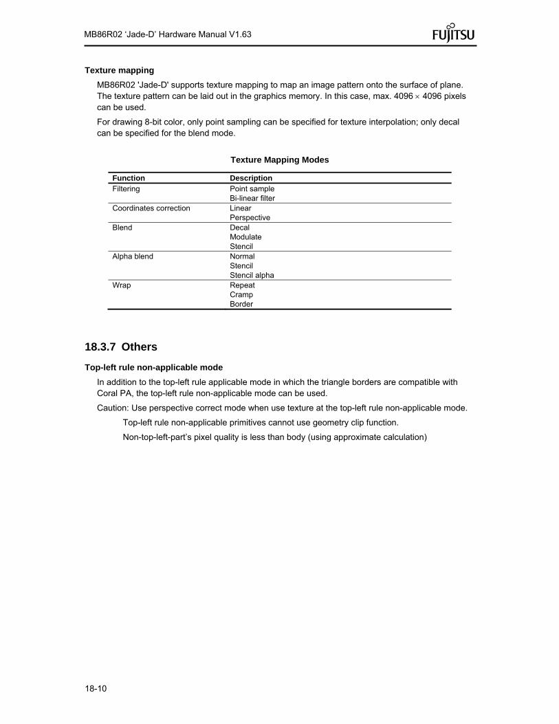
18-10
MB86R02 ‘Jade-D’ Hardware Manual V1.63
Texture mapping
MB86R02 'Jade-D' supports texture mapping to map an image pattern onto the surface of plane. The texture pattern can be laid out in the graphics memory. In this case, max. 4096 4096 pixels can be used.
For drawing 8-bit color, only point sampling can be specified for texture interpolation; only decal can be specified for the blend mode.
Texture Mapping Modes
Function Description Filtering Point sample
Bi-linear filter Coordinates correction Linear
Perspective Blend Decal
Modulate Stencil
Alpha blend Normal Stencil Stencil alpha
Wrap Repeat Cramp Border
18.3.7 Others
Top-left rule non-applicable mode
In addition to the top-left rule applicable mode in which the triangle borders are compatible with Coral PA, the top-left rule non-applicable mode can be used.
Caution: Use perspective correct mode when use texture at the top-left rule non-applicable mode.
Top-left rule non-applicable primitives cannot use geometry clip function.
Non-top-left-part’s pixel quality is less than body (using approximate calculation)

18-11
MB86R02 ‘Jade-D’ Hardware Manual V1.63
18.4 Graphics Memory
18.4.1 Memory map
The memory map for MB86R02 'Jade-D' is extended over that of the MB86296 (Coral PA) as follows; the register area and the VRAM area are separated in the MB86R02 'Jade-D' memory map. Two VRAM segment areas are mapped for MB86R02 'Jade-D' GDC.
Registers
(1)MB86296(Coral-PA)
64MB
F1FF_FFFFH
F1FC_0000H
Registers
4800_0000H
4000_0000H
128MB
VRAM area Register area
(2)MB86R02
Reserved
4400_0000H
Segment 1
(64MB)
Segment 0
(64MB)

18-12
MB86R02 ‘Jade-D’ Hardware Manual V1.63
18.4.2 Configuration
The MB86R02 'Jade-D' uses local external memory (graphics memory) for drawing and display management. The configuration of this graphics memory is described below.
18.4.3 Data Type
The MB86R02 'Jade-D' handles the types of data described below. Display lists can also be stored in the host (main) memory. Texture/tile patterns and text patterns can also be defined by a display list. Drawing Frame This is a rectangular image data field for 2D/3D drawing. The MB86R02 'Jade-D' can have multiple drawing frames and display only a part of these areas if they are configured larger than the display size. The maximum size is 4096x4096 pixel in 32 pixel units. Both indirect color (8 bits / pixel) and direct color (16 bits / pixel) modes are available. Display Frame This is a rectangle picture area used for display. The MB86R02 'Jade-D' is able to use up to 6 display layers. Z Buffer A Z buffer is required for the elimination of hidden surfaces. In 16 bit modes, 2 bytes are required per pixel and in 8 bits mode, 1 byte is required per pixel. This area must be cleared before drawing. Polygon Drawing Flag Buffer This area is used for polygon drawing. It requires 1 bit of the memory area per pixel and 1 x-axis line area both in front and behind it. This area must be cleared before use.
In the specific case of using a polygon with a shadow, the required area depends on the geometry view volume clip parameter. (Normally dependa on the drawing clipping parameter) Above “Y resolution” is “Possible_view_clipped_Max_Ydc -Possible_view_clipped_Min_Ydc+1+6”. (+6 margin is required) Displaylist Buffer The displaylist is a list of drawing commands and parameters. Texture Pattern This pattern is used for texture mapping. The maximum size is up to 4096 x 4096 pixels.
Frame buffer, Z buffer, Displaylist and etc
By XRES size
By drawing frame sizy
By XRES size
Frame buffer, Z buffer,Displaylist and etc
Polygon drawing flag area => (Y resolution + 2) * X resolution
Base Address of Polygon Drawing Buffer(PFBR)

18-13
MB86R02 ‘Jade-D’ Hardware Manual V1.63
Cursor Pattern This is used for hardware cursors. The data format is indirect color (8 bits / pixel) mode. The MB86R02 'Jade-D' is able to display two 64 x 64 pixel cursors.
18.4.4 Data Format
Direct Color (16 bits / pixel) This data format describes an RGB value using 5 bits for each component. Bit15 is used as the alpha bit for layer blending.
15 14 13 12 11 10 9 8 7 6 5 4 3 2 1 0
A R G B
Indirect Color (8 bits / pixel) This data format is a color index code for the lookup table (palette).
7 6 5 4 3 2 1 0
Color Code
Z Value It is possible to use 8 bits or 16 bits for a Z value. The data format is 'unsigned integer'. 1) 16 bits mode
15 14 13 12 11 10 9 8 7 6 5 4 3 2 1 0
Unsigned Integer
2) 8 bits mode 7 6 5 4 3 2 1 0
Unsigned Integer
Polygon Drawing Flag This data format is 1 bit per 1 pixel.
15 14 13 12 11 10 9 8 7 6 5 4 3 2 1 0
P15 P14 P13 P12 P11 P10 P9 P8 P7 P6 P5 P4 P3 P2 P1 P0
31 30 29 28 27 26 25 24 23 22 21 20 19 18 17 16
P31 P30 P29 P28 P27 P26 P25 P24 P23 P22 P21 P20 P19 P18 P17 P16

18-14
MB86R02 ‘Jade-D’ Hardware Manual V1.63
Texture / Tile Pattern It is possible to use a pattern in direct color mode (16 bits / pixel) or indirect color mode (8 bits / pixel). 1) Direct color mode (16 bits / pixel) This data format describes an RGB using 5 bits for each element. Bit15 is used as the alpha bit for stencil or stencil blending (texture mapping only).
15 14 13 12 11 10 9 8 7 6 5 4 3 2 1 0
A R G B
2) Indirect color mode (8 bits / pixel) This data format is a color index code into the lookup table (palette).
7 6 5 4 3 2 1 0
Color Code
Cursor Pattern This data format is a color index code into the lookup table (palette).
7 6 5 4 3 2 1 0
Color Code
Video Capture data This data format is Y:Cb:Cr=4:2:2 and 32 bits per 2 pixels.
15 14 13 12 11 10 9 8 7 6 5 4 3 2 1 0
Y0 Cb
31 30 29 28 27 26 25 24 23 22 21 20 19 18 17 16
Y1 Cr
Direct Color (32 bits / pixel) This data format describes an RGB value with 8 bits for each element. Bit31 is used as an alpha bit of layer blending. MB86R02 'Jade-D' does not support this color mode for drawing. Therefore please draw this layer using CPU writes.
15 14 13 12 11 10 9 8 7 6 5 4 3 2 1 0
G B
31 30 29 28 27 26 25 24 23 22 21 20 19 18 17 16
A Reserved R

18-15
MB86R02 ‘Jade-D’ Hardware Manual V1.63
18.5 Frame Management
18.5.1 Single Buffer
The entire drawing frame (or a part of it) can be assigned as a display frame. The displayed area can be scrolled by relocating the position of the display frame. If the display frame crosses the border of the drawing frame, the opposite side of the drawing frame is displayed, i.e. the drawing frame is rolled over (top and left edges are assumed to be logically connected to the bottom and right edges respectively). To avoid artefacts by drawing directly on the display, drawing data can be transferred to the graphics memory in the blanking time period.
18.5.2 Double Buffer
Two drawing frames are set up. While one frame is being displayed, drawing is done to the other frame. Flicker-less animation can be performed by switching back and forth between these two frames. Switching is done in the blanking time period. There are two switching modes: automatically at every scan frame period or manually by user control. Double buffer is assigned independently for the L2, L3, L4, L5 layers.
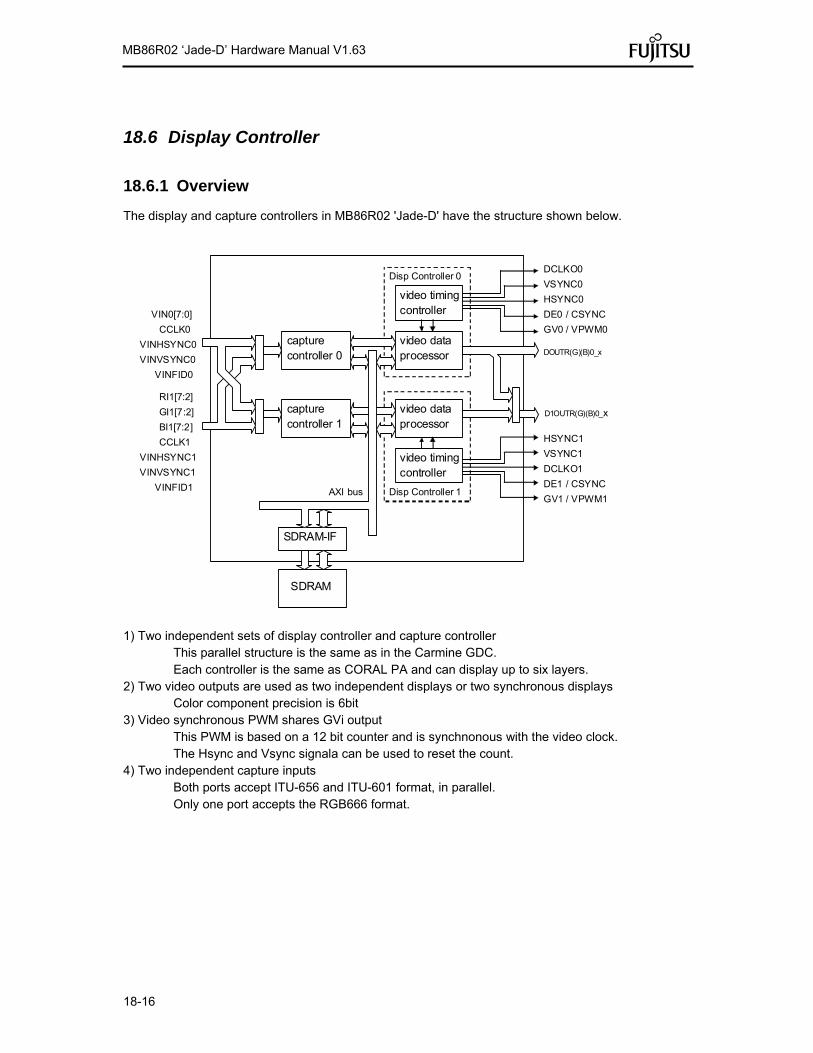
18-16
MB86R02 ‘Jade-D’ Hardware Manual V1.63
18.6 Display Controller
18.6.1 Overview
The display and capture controllers in MB86R02 'Jade-D' have the structure shown below. 1) Two independent sets of display controller and capture controller
This parallel structure is the same as in the Carmine GDC. Each controller is the same as CORAL PA and can display up to six layers.
2) Two video outputs are used as two independent displays or two synchronous displays Color component precision is 6bit
3) Video synchronous PWM shares GVi output This PWM is based on a 12 bit counter and is synchnonous with the video clock. The Hsync and Vsync signala can be used to reset the count.
4) Two independent capture inputs Both ports accept ITU-656 and ITU-601 format, in parallel. Only one port accepts the RGB666 format.
video timing controller
video data processor
video data processor
video timing controller DCLKO1
HSYNC1
VSYNC1
DOUTR(G)(B)0_x
AXI bus
SDRAM-IF
SDRAM
Disp Controller 0
Disp Controller 1
HSYNC0
VSYNC0
DCLKO0
DE0 / CSYNC
capture controller 0
capture controller 1
CCLK0
VIN0[7:0]
RI1[7:2]
CCLK1
VINHSYNC0
VINFID0
DE1 / CSYNC
GV1 / VPWM1
GV0 / VPWM0
VINVSYNC0
GI1[7:2]
BI1[7:2]
VINHSYNC1
VINFID1
VINVSYNC1
D1OUTR(G)(B)0_x
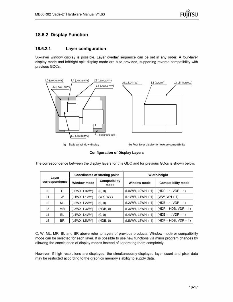
18-17
MB86R02 ‘Jade-D’ Hardware Manual V1.63
18.6.2 Display Function
18.6.2.1 Layer configuration
Six-layer window display is possible. Layer overlay sequence can be set in any order. A four-layer display mode and left/right split display mode are also provided, supporting reverse compatibility with previous GDCs.
Configuration of Display Layers
The correspondence between the display layers for this GDC and for previous GDcs is shown below.
Layer correspondence
Coordinates of starting point Width/height
Window mode Compatibility
mode Window mode Compatibility mode
L0 C (L0WX, L0WY) (0, 0) (L0WW, L0WH 1) (HDP 1, VDP 1)
L1 W (L1WX, L1WY) (WX, WY) (L1WW, L1WH 1) (WW, WH 1)
L2 ML (L2WX, L2WY) (0, 0) (L2WW, L2WH 1) (HDB 1, VDP 1)
L3 MR (L3WX, L3WY) (HDB, 0) (L3WW, L3WH 1) (HDP HDB, VDP 1)
L4 BL (L4WX, L4WY) (0, 0) (L4WW, L4WH 1) (HDB 1, VDP 1)
L5 BR (L5WX, L5WY) (HDB, 0) (L5WW, L5WH 1) (HDP HDB, VDP 1)
C, W, ML, MR, BL and BR above refer to layers of previous products. Window mode or compatibility mode can be selected for each layer. It is possible to use new functions via minor program changes by allowing the coexistence of display modes instead of separating them completely.
However, if high resolutions are displayed, the simultaneously-displayed layer count and pixel data may be restricted according to the graphics memory's ability to supply data.
L0 (L0WX,L0WY) L2 (L2WX,L2WY)
L1 (L1WX,L1WY)L5 (L5WX,L5WY)
L4 (L4WX,L4WY)
L3 (L3WX,L3WY)
(a) Six layer window display
L0,L2,L4 (0,0) L3,L5 (HDB+1,0) L1 (WX,WY)
(b) Four layer display for reverse compatibility
background color
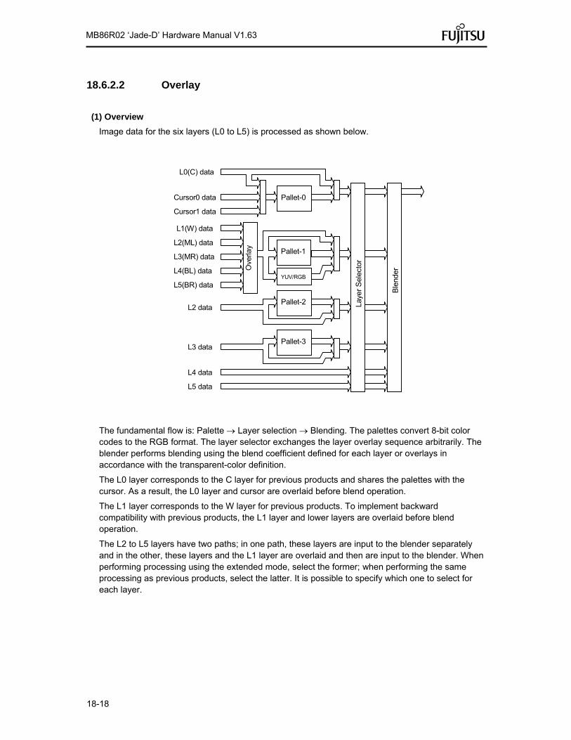
18-18
MB86R02 ‘Jade-D’ Hardware Manual V1.63
18.6.2.2 Overlay
(1) Overview
Image data for the six layers (L0 to L5) is processed as shown below.
The fundamental flow is: Palette Layer selection Blending. The palettes convert 8-bit color codes to the RGB format. The layer selector exchanges the layer overlay sequence arbitrarily. The blender performs blending using the blend coefficient defined for each layer or overlays in accordance with the transparent-color definition.
The L0 layer corresponds to the C layer for previous products and shares the palettes with the cursor. As a result, the L0 layer and cursor are overlaid before blend operation.
The L1 layer corresponds to the W layer for previous products. To implement backward compatibility with previous products, the L1 layer and lower layers are overlaid before blend operation.
The L2 to L5 layers have two paths; in one path, these layers are input to the blender separately and in the other, these layers and the L1 layer are overlaid and then are input to the blender. When performing processing using the extended mode, select the former; when performing the same processing as previous products, select the latter. It is possible to specify which one to select for each layer.
Pallet-1
YUV/RGB
Pallet-2
Pallet-3
Pallet-0
Laye
r S
elec
tor
L0(C) data
L2(ML) data
Cursor0 data
L2 data
L3 data
L4 data
L5 data B
lend
er Ove
rlay
Cursor1 data
L1(W) data
L4(BL) data
L3(MR) data
L5(BR) data

18-19
MB86R02 ‘Jade-D’ Hardware Manual V1.63
(2) Overlay mode
Image layer overlay is performed in two modes: simple priority mode and blend mode.
In the simple priority mode, processing is performed according to the transparent color defined for each layer. When the color is a transparent color, the value of the lower layer is used as the image value for the next stage; when the color is not a transparent color, the value of the layer is used as the image value for the next stage.
Dview = Dnew (when Dnew does not match transparent color)
= Dlower (when Dnew matches transparent color)
When the L1 layer is in the YCbCr mode, transparent color checking is not performed for the L1 layer; processing is always performed assuming that transparent color is not used.
In the blend mode, the blend ratio “r” defined for each layer is specified using 8-bit tolerance and the following operation is performed:
Dview = Dnewr + Dlower (1 – r)
Blending is enabled for each layer by mode setting and a specific bit of the pixel is set to “1”. For 8 bits/pixel, the MSB of RAM data enables blending; for 16 bits/pixel, the MSB of data of the relevant layer enables blending; for 24 bits/pixel, the MSB of the word enables blending.
(3) Blend coefficient layer
In the normal blend mode, the blend coefficient is fixed for each layer. However, in the blend coefficient layer mode, the L5 layer can be used as the blend coefficient layer. In this mode, the blend coefficient can be specified for each pixel, providing gradation, for example. When using this mode, set the L5 layer to 8 bits/pixel, widow display mode and extend overlay mode.
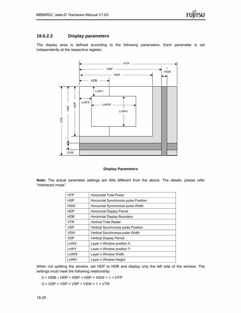
18-20
MB86R02 ‘Jade-D’ Hardware Manual V1.63
18.6.2.3 Display parameters
The display area is defined according to the following parameters. Each parameter is set independently at the respective register.
HTP
HSP
HDB
HDP
LnWY
LnWX LnWW
LnWH
VD
P
VS
P
VT
R
VSW
HSW
Display Parameters
Note: The actual parameter settings are little different from the above. The details, please refer “Interlaced mode”.
HTP Horizontal Total Pixels
HSP Horizontal Synchronize pulse Position
HSW Horizontal Synchronize pulse Width
HDP Horizontal Display Period
HDB Horizontal Display Boundary
VTR Vertical Total Raster
VSP Vertical Synchronize pulse Position
VSW Vertical Synchronize pulse Width
VDP Vertical Display Period
LnWX Layer n Window position X
LnWY Layer n Window position Y
LnWW Layer n Window Width
LnWH Layer n Window Height
When not splitting the window, set HDP to HDB and display only the left side of the window. The settings must meet the following relationship:
0 < HDB HDP < HSP < HSP + HSW + 1 < HTP
0 < VDP < VSP < VSP + VSW + 1 < VTR
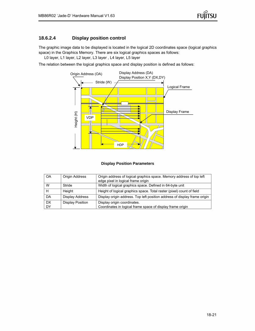
18-21
MB86R02 ‘Jade-D’ Hardware Manual V1.63
18.6.2.4 Display position control
The graphic image data to be displayed is located in the logical 2D coordinates space (logical graphics space) in the Graphics Memory. There are six logical graphics spaces as follows:
L0 layer, L1 layer, L2 layer, L3 layer , L4 layer, L5 layer
The relation between the logical graphics space and display position is defined as follows:
Display Position Parameters
OA Origin Address Origin address of logical graphics space. Memory address of top left
edge pixel in logical frame origin W Stride Width of logical graphics space. Defined in 64-byte unit
H Height Height of logical graphics space. Total raster (pixel) count of field
DA Display Address Display origin address. Top left position address of display frame origin
DX DY
Display Position Display origin coordinates. Coordinates in logical frame space of display frame origin
Stride (W)
Hei
ght
(H)
Origin Address (OA) Display Address (DA) Display Position X,Y (DX,DY)
VDP
Logical Frame
Display Frame
HDP

18-22
MB86R02 ‘Jade-D’ Hardware Manual V1.63
The display controller scans the logical graphics space as if the entire space is rolled over in both the horizontal and vertical directions. Using this function, if the display frame crosses the border of the logical graphics space, the part outside the border is covered with the other side of the logical graphics space, which is assumed to be connected cyclically as shown below:
Wrap Around of Display Frame
The expression of the X and Y coordinates in the frame and their corresponding linear addresses (in bytes) is shown below.
A(x,y) = x bpp/8 + 64wy (bpp = 8 or 16)
The origin of the displayed coordinates has to be within the frame. To be more specific, the parameters are subject to the following constraints:
0 DX < w 64 8/bpp (bpp = 8 or 16)
0 DY < H
DX, DY and DA have to indicate the same point within the frame. In short, the following relationship must be satisfied.
DA = OA + DX bpp/8 + 64w DY (bpp = 8 or 16)
64 w
L
Logical Frame Origin
Additionally drawn area New display origin
Previous display origin
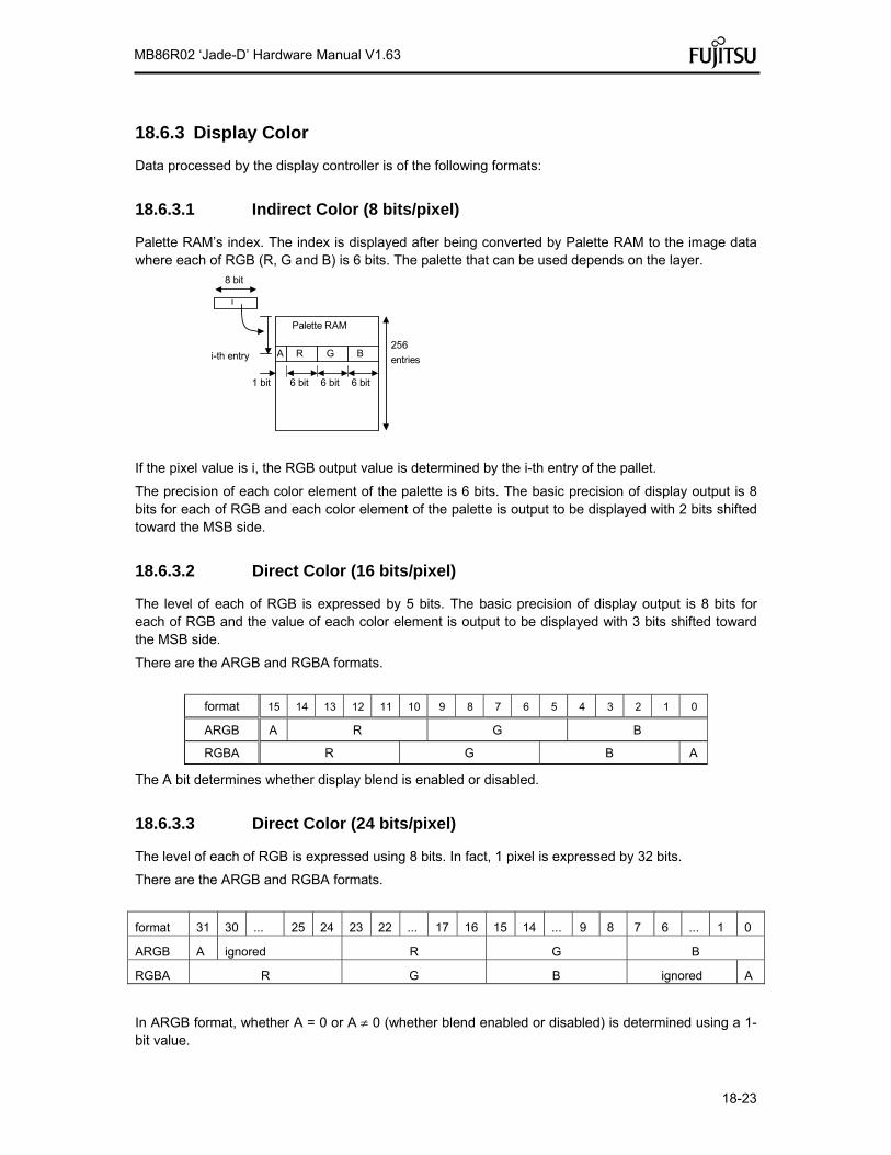
18-23
MB86R02 ‘Jade-D’ Hardware Manual V1.63
18.6.3 Display Color
Data processed by the display controller is of the following formats:
18.6.3.1 Indirect Color (8 bits/pixel)
Palette RAM’s index. The index is displayed after being converted by Palette RAM to the image data where each of RGB (R, G and B) is 6 bits. The palette that can be used depends on the layer.
A
8 bit
R G Bi-th entry
i
1 bit 6 bit 6 bit 6 bit
Palette RAM
256
entries
If the pixel value is i, the RGB output value is determined by the i-th entry of the pallet.
The precision of each color element of the palette is 6 bits. The basic precision of display output is 8 bits for each of RGB and each color element of the palette is output to be displayed with 2 bits shifted toward the MSB side.
18.6.3.2 Direct Color (16 bits/pixel)
The level of each of RGB is expressed by 5 bits. The basic precision of display output is 8 bits for each of RGB and the value of each color element is output to be displayed with 3 bits shifted toward the MSB side.
There are the ARGB and RGBA formats.
format 15 14 13 12 11 10 9 8 7 6 5 4 3 2 1 0
ARGB A R G B
RGBA R G B A
The A bit determines whether display blend is enabled or disabled.
18.6.3.3 Direct Color (24 bits/pixel)
The level of each of RGB is expressed using 8 bits. In fact, 1 pixel is expressed by 32 bits.
There are the ARGB and RGBA formats.
format 31 30 ... 25 24 23 22 ... 17 16 15 14 ... 9 8 7 6 ... 1 0
ARGB A ignored R G B
RGBA R G B ignored A
In ARGB format, whether A = 0 or A 0 (whether blend enabled or disabled) is determined using a 1-bit value.

18-24
MB86R02 ‘Jade-D’ Hardware Manual V1.63
Refer to the descriptions of the indivdual layer extended color modes for information on how to select RBGA modes (e.g. bitfield L0EC in register L0EM).
In ARGB format, whether A = 0 or A 0 (whether blend enabled or disabled) is determined using an 8-bit integer value.
18.6.3.4 YCbCr Color (16 bits/pixel)
Image data of “YcbCr = 4:2:2” format. This image data is displayed after being converted by the calculation circuit to the image data where each of RGB is 8 bits. 2 pixels, each being RGB 24 bits, are expressed by 32 bits. As a result, the image data can be processed as 16 bits/pixel.
format 31 30 25 24 23 22 17 16 15 14 9 8 7 6 1 0
YCbCr Y Cr Y Cb
18.6.3.5 Alpha factor (8 bits/pixel)
The factor for display blend is held. When the value is t, t/256 is expressed as a binary fraction. During display blend, the following calculation is performed for each color element of each pixel:
c’ = c0t/256 + c1 (1-t/256)
18.6.3.6 Layer dependence
The display colors for each layer are shown below.
Layer Compatibility mode Extended mode
L0 Direct color (16, 24), Indirect color (P0) Direct color (16, 24), Indirect color (P0)
L1 Direct color (16, 24), Indirect color (P1), YCbCr Direct color (16, 24), Indirect color (P1), YCbCr
L2 Direct color (16, 24), Indirect color (P1) Direct color (16, 24), Indirect color (P2)
L3 Direct color (16, 24), Indirect color (P1) Direct color (16, 24), Indirect color (P3)
L4 Direct color (16, 24), Indirect color (P1) Direct color (16, 24)
L5 Direct color (16, 24), Indirect color (P1) Direct color (16, 24)
“Pn” stands for the corresponding palette RAM. Four palettes are used as follows:
1) Palette 0 (P0)
This palette corresponds to the C-layer palette for previous products. This palette is used for the L0 layer. This palette can also be used for the cursor.
2) Palette 1 (P1)
This palette corresponds to the M/B layer palette for previous products. In the compatibility mode, this palette is common to layers L1 to 5. In the extended mode, this palette is dedicated to the L1 layer.
3) Palette 2 (P2)
This palette is dedicated to the L2 layer. This palette can be used only for the extended mode.
4) Palette 3 (P3)
This palette is dedicated to the L3 layer. This palette can be used only for the extended mode.

18-25
MB86R02 ‘Jade-D’ Hardware Manual V1.63
18.6.4 Cursor
18.6.4.1 Cursor display function
The display controller can display two hardware cursors. Each cursor is specified as 64 64 pixels and the cursor pattern is set in the Graphics Memory. The indirect color mode (8 bits/pixel) is used and the L0 layer palette is used. However, transparent color control (handling of transparent color code and code 0) is independent of L0 layer. Blending with lower layer is not performed.
18.6.4.2 Cursor control
The display priority for hardware cursors is programmable. The cursor can be displayed either on upper or lower the L0 layer using this feature. A separate setting can be made for each hardware cursor. If part of a hardware cursor crosses the display frame border, the part outside the border is not shown.
Usually, cursor 0 is preferred to cursor 1. However, with cursor 1 displayed upper the L0 layer and cursor 0 displayed lower the L0 layer, the cursor 1 display is preferred to the cursor 0.
18.6.5 Display Scan Control
18.6.5.1 Applicable display
The following table shows typical display resolutions and their synchronous signal frequencies. The pixel clock frequency is determined by setting the division rate of the display reference clock. The display reference clock is either the internal PLL (e.g. 533.3 MHz at input frequency of 25.0 MHz), or the clock supplied to the DCLKI input pin. The following table gives the clock division rate used when the internal PLL is the display reference clock:
Example of Resolution and Display Frequency
Resolution Division rate of reference
clock
Pixel frequency
Horizontal total pixel
count
Horizontal frequency
Vertical total raster
count
Vertical frequency
320 240 1/20/41 6.7 MHz 424 15.80 kHz 263 59.9 Hz
...
1024 768 1/8 66.7 MHz 1389 48.02 kHz 806 59.9 Hz
Pixel frequency = 25.0 MHz / 3 64 reference clock division rate (when internal PLL selected)
= DCLKI input frequency reference clock division rate (when DCLKI selected)
Horizontal frequency = Pixel frequency/Horizontal total pixel count
Vertical frequency = Horizontal frequency/Vertical total raster count
1 Use bit 14 of DCM1 to select additional pre-divider factor 4

18-26
MB86R02 ‘Jade-D’ Hardware Manual V1.63
18.6.5.2 Interlace display
The display controller can perform both a non-interlace display and an interlace display.
When the DCM register synchronization mode is set to interlace video (11), images in memory are output in odd and even rasters alternately to each field and one frame (odd + even fields) forms one screen.
When the DCM register synchronization mode is set to interlace (10), images in memory are output in raster order. The same image data is output to odd fields and even fields. Consequently, the count of rasters on the screen is half of that of interlace video. However, unlike the non-interlace mode, there is a distinction between odd and even fields depending on the phase relationship between the horizontal and vertical synchronous signals.
Display Difference between Synchronization Modes
Odd
Even
Non-Interlace Interlace Video Interlace

18-27
MB86R02 ‘Jade-D’ Hardware Manual V1.63
18.6.6 Programmable YCbCr/RGB conversion for L1-layer display
L1-layer can display video data in YCbCr format but RGB conversion coefficients are hard-wired and fixed about previous products. MB86R02 'Jade-D' can program RGB conversion coefficients by registers.
YCbCr data is converted by following expression.
R = a11Y + a12(Cb128) + a13(Cr128) + b1
G = a21Y + a22(Cb128) + a23(Cr128) + b2
B = a31Y + a32(Cb128) + a33(Cr128) + b3
aij ---- 11bit signed real (lower 8bit is fraction, two's complement)
bi ----- 9bit signed integer (two's complement)
It is represended by matrix operation.
These parameters are set on registers shown bellow.
L1YCR0 (a12,a11), L1YCR1(b1,a13)
L1YCG0 (a22,a21), L1YCG1(b2,a23)
L1YCB0 (a32,a31), L1YCB1(b3,a33)
Same conversion with previous products is applied by initial values of these registers after reset.
The register values just after reset is as follow.
a11 = 0x12b (299/256) , a12 = 0x0, a13 = 0x198 (408/256)
a21 = 0x12b (299/256), a22 = 0x79c (-100/256), a23 = 0x72f (-209/256)
a31 = 0x12b (299/256), a32 = 0x204 (516/256), a33 = 0x0
b1= b2= b3= 0x1f0 (-16)
It is possible to control brightness, contrast, hue , color saturation by change these parameters.
Addition of a constant value into b means inclease of brightness.
Multiplication of a constant scalar value greater than one into A means increase of contrast.
Two dimentional rotation of Cb-128 and Cr-128 means change of hue.
Color saturation is intensity of color, relative to Y-component.
New coefficients including these changes can be got by following expression.
R G B
a11
a21
a31
a12
a22
a32
a13
a23
a33
Y Cb-128 Cr-128
where , b =
b1
b2
b3
= A + b A =

18-28
MB86R02 ‘Jade-D’ Hardware Manual V1.63
A0 , b0 : initial value
c1: contrast parameter, 1 is standard. 1.2 is stronger, for example.
c2: color saturation parameter, 1 is standard. 0 means mono chrome image.
c3: brightness parameter, 0 is standard.
t : hue rotation parameter, 0-deg is standard
Note: new aij and bi should be clipped in valid range of value for corresponding registers.
100
0 cos(t) -sin(t)
0 sin(t) cos(t)
A = c1 A0
b = bo + c3 c3 c3
100
0c2
0
00c2
= A0
c1
00
0cos(t)c1c2
-sin(t)c1c2
0sin(t)c1c2
cos(t)c1c2

18-29
MB86R02 ‘Jade-D’ Hardware Manual V1.63
18.6.7 DCLKO shift
1) Delay
If the internal PLL is used to generate the DCLK, then it is possible to delay the DCLKO signal. The DCKD field in the DCM3 register defines a delay value in units of internal PLL clock cycles.
DCKD (value in hex.) Delay
0x00 No delay (res)
0x02 +1 PLL clock
0x04 +2 PLL clocks
0x06 +3 PLL clocks
0x08 +4 PLL clocks
0x0A +5 PLL clocks
0x0C +6 PLL clocks
0x0E +7 PLL clocks
0x10 +8 PLL clocks
0x12 +9 PLL clocks
0x14 +10 PLL clocks
0x16 +11 PLL clocks
0x18 +12 PLL clocks
0x1A +13 PLL clocks
0x1C +14 PLL clocks
0x1E +15 PLL clocks
2) Inversion
DCLKO inversion is also available with or without the delay functionality. This function is effective without regard to the DCLK clock source.
The DCKinv bit of DCM3 enables this function.
18.6.8 Synchronous register updates and display
To update position related parameters without disturbing the display, it is necessary to update in synch with the VSYNC interrupt and to complete this in time.
This synchronous register update mode eases this limitation. In this mode, written parameters are hold in intermediate registers and update at once synchronously with VSYNC.
RUM-bit of DCM2 register enables this mode.
RUF-bit of DCM2 register controls start of update and shows whether update is done or not.

18-30
MB86R02 ‘Jade-D’ Hardware Manual V1.63
18.6.9 Parallel Dual Display
MB86R02 'Jade-D' incorporates two independent display controllers that operate in parallel.
screen"1"
screen"0"display device"0"
display device"1"
MB86R02
display controller 0
display controller 1
If only using one output, se the display enable flag in DCM0/1 register to zero for the unsed display controller. The two display controllers work independently, therefore different resolutions can be used by each controller and therefore each works asynchronously to the other.
VSYNC0
VSYNC1
interrupt
interrupt
The phase difference indicated above of each frame should be taken into consideration when drawing figures synchronously on two screens.
This assumes that the controllers have the same timing parameters and share the same clock source such as the internal PLL.
If the 'display enable' flags of the controllers are activated sequentially, then the phase difference of VSYNC will remain very small and stays constant.
Note:
Dual Display functionality is not possible with RSDS panels.
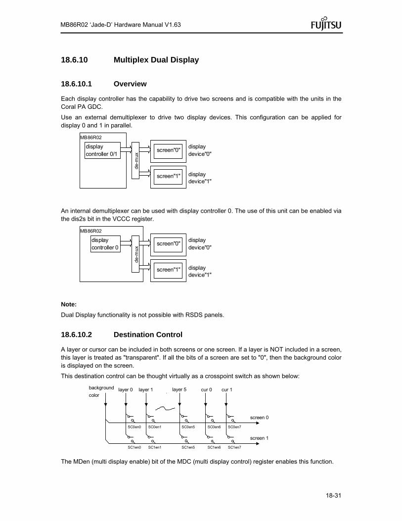
18-31
MB86R02 ‘Jade-D’ Hardware Manual V1.63
18.6.10 Multiplex Dual Display
18.6.10.1 Overview
Each display controller has the capability to drive two screens and is compatible with the units in the Coral PA GDC.
Use an external demultiplexer to drive two display devices. This configuration can be applied for display 0 and 1 in parallel.
screen"1"
screen"0"display device"0"
display device"1"
MB86R02
display controller 0/1
de-m
ux
An internal demultiplexer can be used with display controller 0. The use of this unit can be enabled via the dis2s bit in the VCCC register.
screen"1"
screen"0"display device"0"
display device"1"
MB86R02
display controller 0
de-m
ux
Note:
Dual Display functionality is not possible with RSDS panels.
18.6.10.2 Destination Control
A layer or cursor can be included in both screens or one screen. If a layer is NOT included in a screen, this layer is treated as "transparent". If all the bits of a screen are set to "0", then the background color is displayed on the screen.
This destination control can be thought virtually as a crosspoint switch as shown below:
SC0en6
SC1en6
SC0en7
SC1en7
SC0en5
SC1en5
SC0en1
SC1en1
SC0en0
SC1en0
screen 0
layer 0
screen 1
background
color layer 1 layer 5 cur 0 cur 1
The MDen (multi display enable) bit of the MDC (multi display control) register enables this function.

18-32
MB86R02 ‘Jade-D’ Hardware Manual V1.63
The SC0en (screen"0" enable) field of the MDC register defines which layers and cursors are included in screen “0”.
The SC1en (screeen"1" enable) field of the MDC register defines which layers and cursors are included in screen “1”.
bit-0 ---- L0 is included
bit-1 ---- L1 is included
:
bit-5 ---- L5 is included
bit-6 ---- Cursor0 is included
bit-7 ---- Cursor1 is included
18.6.10.3 Output Signal Control
Two screen data streams are output in multiplex mode as follows:
sc0 sc1DRn,DGn,DBn
DCLKOn
HSYNCn
even clocks
DEn
ref edge
sc0 is first
18.6.10.4 Output Circuit Example
A single CPLD can demultiplex the RGB 6bit/component video data stream (Xilinx device shown here):
DCKi
VSi
HSi
Di[18]
DCK0
VS0
HS0
D0[18]
D0[17:0]Di[17:0]
DRn[7:2]
DGn[7:2]
DBn[7:2]
DCLKOn
HSYNCn
VSYNCn
DEn
XC9572XL-TQ100
R0,G0,B0
DCLK0 HSYNC0VSYNC0DE0
R1,G1,B1
DCLK1 HSYNC1VSYNC1DE1
(SE mode)
MB86R02
display device "0"
display device "1"
D1[17:0]
DCK1
VS1
HS1
D1[18]
(POM=0,DCKed=0)

18-33
MB86R02 ‘Jade-D’ Hardware Manual V1.63
module XC9572XL (DCKi, HSi,VSi,Di, DCK0,HS0,VS0,D0, DCK1,HS1,VS1,D1);
input DCKi,HSi,VSi;
input[18:0] Di;
output DCK0,HS0,VS0, DCK1,HS1,VS1;
output[18:0] D0,D1;
reg HS0,HS1, VS0,VS1, DCK0,DCK1;
reg[18:0] D0,D1;
always @(posedge DCKi) begin
HS0 <= HSi; HS1 <= HS0;
VS0 <= VSi; VS1 <= VS0;
DCK0 <= (HS0&!HSi)? 0: !DCK0; // sync to ref edge : flip
DCK1 <= DCK0;
if(DCK0) D0 <= Di;
if(DCK1) D1 <= Di;
end
endmodule
Di
DCLKi
HSi
even clocks
ref edge
sc0 sc1 sc0 sc1 sc1
sc0 sc0
sc1 sc1
DCK0
D0[18:0]
DCK1
D1[18:0]
read point
read point

18-34
MB86R02 ‘Jade-D’ Hardware Manual V1.63
18.6.10.5 Display Clock and Timing
It is necessary to supply a display clock of twice the frequency for dual display functionality. VGA display typically uses a 25MHz display clock in single display mode whereas a 50MHz display clock is required for dual display mode. The timing parameters such as HTP except the scaling ratio (SC) should be the same.
The maximum display clock frequency determines the maximum resolution available. For 800 x 480, a 66MHz DCLK clock is required.
18.6.10.6 Limitations
For multiplex dual display, two display devices must have the same scan rate and resolution with common sync signals.
The external sync mode can not be used in multiplex dual display mode.
The external sync mode can not be used together when the TCON of the MB86R02 'Jade-D' TCON is active. Using external sync mode together with an active TCON creates an instable horizontal back porch.
18.6.10.7 Dual display configuration example
Single display
In the case of a single display application, set the DEN bit to '1' for the single display controller to be used. Multiplex dual display mode has to be disabled. The following example shows the settings for the use of display controller 0 only.
DCM1 DCM3 MDC
DEN-bit POM-bit DCKed-bit MDen-bit SCnEN-field
DISP0 1 0 0 0 Don’t care
DISP1 0 Don’t care Don’t care Don’t care Don’t care
Common VCCC/dis2s=0
Using display controller 1 instead if of course possible.
Parallel dual display (no multiplex) In the case of parallel dual display without multiplex, enable the DEN bit for both display controllers. Multiplex dual display mode has to be disabled.
DCM1 DCM3 MDC
DEN-bit POM-bit DCKed-bit MDen-bit SCnEN-field
DISP0 1 0 0 0 Don’t care
DISP1 1 0 0 0 Don’t care
Common VCCC/dis2s=0
Multiplex dual display ( internal demultiplex ) In the case of multiplex dual display with an internal demultiplexer, enable the DEN-bit for display controller 0. Multiplex dual display mode has to be enabled. The multiplexed video stream from

18-35
MB86R02 ‘Jade-D’ Hardware Manual V1.63
display controller 0 is demultplexed internally and output on the two video output ports. Two video output ports are used only for display controller 0 so display controller 1 can not be used.
DCM1 DCM3 MDC
DEN-bit POM-bit DCKed-bit MDen-bit SCnEN-field
DISP0 1 1 1 1 Valid
DISP1 0 Don’t care Don’t care Don’t care Don’t care
Common VCCC/dis2s=1
Note that the external synchronization mode of display controller 1 has to be disabled to output HSYNC1 and VSYNC1.
Multiplex dual display (external demultiplex)
In the case of multiplex dual display with an external demultiplexer, one or both display controllers can be used. The example shows display controller 0 in use in single display mode and display controller 1 in use in multiplex dual display mode.
DCM1 DCM3 MDC
DEN-bit POM-bit DCKed-bit MDen-bit SCnEN-field
DISP0 1 0 0 0 Don’t care
DISP1 1 0 0 1 Valid
Common VCCC/dis2s=0
If two display controllers are used in multiplex dual display mode, four display screens can be used.
18.6.11 Video output limitation
Due to the limited number of package pins, the available video output is limitted as follows.
Display controller 0: RGB888 (R[7:0], G[7:0], B[7:0])
Display controller 1: RGB666 (R[7:2], G[7:2], B[7:2])
See “Pin Multiplex Mode” for details.
18.6.12 Interrupt
The primary interrupt functions for Jade-D display and capture are the same as for Coral PA except that there are two controllers. The IST (interrupt status register) bit allocation is as follows:
bit 0 CERR (Command Error Flag)
bit 1 CEND (Command End)
bit 2 VSYNC0 of display 0
bit 3 FSYNC0 of display 0
bit 4 SYNCERR0 of display 0
bit 5 REGUD0 of display 0
bit 6 VSYNC1 of display 1
bit 7 FSYNC1 of display 1

18-36
MB86R02 ‘Jade-D’ Hardware Manual V1.63
bit 8 SYNCERR1 of display 1
bit 9 REGUD1 of display 1
bit 10 Capture 0
bit 11 Capture 1
The host address offset of the IST register is 0x20.
The offset address of the corresponding register for interrupt masking (IMASK) is 0x24. It has same bit allocation.

18-37
MB86R02 ‘Jade-D’ Hardware Manual V1.63
18.7 Video Capture
18.7.1 Video Capture function
18.7.1.1 Input data Formats
A digital video stream in ITU RBT-656 or RGB666 standard format can be input (for details refer to the section 'External video signal input conditions').
18.7.1.2 Video Signal Capture
The capture controller works when the VIE bit of the video capture mode register (VCM) is 1 and CCLK is enabled. Video stream data is then captured on the 8-bit VI pin or 20-bit RGB input pin in sync with the clock.
18.7.1.3 Non-interlace Transformation
Captured video graphics can be displayed in non-interlaced format. One of two modes (BOB and WEAVE) can be selected for non-interlace transformation.
- BOB Mode
In odd fields, the even-field raster generated by average interpolation are added to produce one frame. In even fields, the odd-field raster generated by average interpolation are added to produce one frame.
In order to choose BOB mode, while enable vertical interpolation in VI bit of a VCM (Video Capture Mode) register, the L1IM bit of L1M (L1-layer Mode) register is set as 0.
- WEAVE Mode
Odd and even fields are merged in the video capture buffer to produce one frame. Vertical resolutions in the WEAVE mode are higher than those in the BOB mode but raster dislocation appears at moving places.
In order to choose WEAVE mode, while disable vertical interpolation in VI bit of a VCM (Video Capture Mode) register, the L1IM bit of L1M (L1-layer Mode) register is set to 1.

18-38
MB86R02 ‘Jade-D’ Hardware Manual V1.63
18.7.2 Input Port Selection
Jade-D has two independent capture units. The input port has two systems and an application can switch between them.
RI1 [7:2], GI1 [7:2],
CCLK1
CCLK0
VIN0 [7:0]
display controller 0
capture controller 0
capture controller 1
display controller 1
656 / 601
RGB/656/601
VINHSYNC0
VINVSYNC0
BI1 [7:2]
VINHSYNC1
VINVSYNC1
VINFID0
VINFID1
One capture input port can be used for 656 format only, whereby the other can select between RGB format and 656 format.
To use 656 input via the port which can handle both RGB and 656, check the pin multiplex tables in this Hardware Manual to obtain the details about external pin routing.
Use the VIS bit of the VCM register to select RGB or 656 input.
The input port is selected using the Csel0/1 bit of the VCCC (Video/Capture Common Control) register.
Csel0 = 0: 656 input Capture 0
Csel0 = 1: RGB/656 input Capture 0
Csel1 = 0: 656 input Capture 1
Csel1 = 1: RGB/656 input Capture 1
Selection examples are shown below.
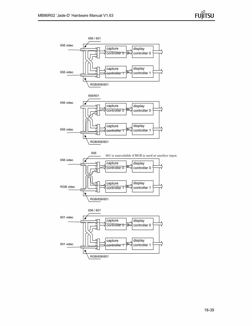
18-39
MB86R02 ‘Jade-D’ Hardware Manual V1.63
656 video
656 video
display controller 0
capture controller 0
capture controller 1
display controller 1
656 / 601
RGB/656/601
656 video
656 video
display controller 0
capture controller 0
capture controller 1
display controller 1
656/601
RGB/656/601
656 video
RGB video
display controller 0
capture controller 0
capture controller 1
display controller 1
656
RGB/656/601
601 is unavailable if RGB is used at another input
601 video
601 video
display controller 0
capture controller 0
capture controller 1
display controller 1
656 / 601
RGB/656/601

18-40
MB86R02 ‘Jade-D’ Hardware Manual V1.63
18.7.3 Video Buffer
18.7.3.1 Data Format
Data is stored in the capture buffer in a 16 bits/pixel format. Two color components (Cb, Cr) are respectively half the resolution of the luma data (Y component) in the horizontal direction. As the table below shows 32 bits, it therefore holds the data for two pixels.
Note that for the L1 layer, data is converted to the RGB format before it is displayed.
format 31 30 25 24 23 22 17 16 15 14 9 8 7 6 1 0
YCbCr 16 bit/pixel Y Cr Y Cb
Data can also be stored in an RGB format, assuming that the drawing unit uses the data as a texture. The following formats are used:
format 15 14 13 12 11 10 9 8 7 6 5 4 3 2 1 0
ARGB 16 bits/pixel A R G B
RGBA 16 bits/pixel R G B A
format 31 30 25 24 23 22 17 16 15 14 9 8 7 6 1 0
ARGB 24 bits/pixel A ignored R G B
RGBA 24 bits/pixel R G B A
The relationship between the capture data formats and the data format control bits in registers is shown below:
NRGB1 CRGB2 C242 RGBA Capture data format up-scaling
0 0 0 0 YcbCr 16 bits/pixel
0 0 0 1 Unused
0 0 1 x Unused
0 1 0 0 ARGB 16 bits/pixel (YCbCr RGB conversion)
0 1 0 1 RGBA 16 bits/pixel (YCbCr RGB conversion)
0 1 1 0 ARGB 24 bits/pixel (YCbCr RGB conversion)
0 1 1 1 RGBA 24 bits/pixel (YCbCr RGB conversion)
1 0 0 0 ARGB 16 bits/pixel
1 0 0 1 RGBA 16 bits/pixel
1 0 1 0 ARGB 24 bits/pixel
1 0 1 1 RGBA 24 bits/pixel
1 1 x x Unused 1NRGB = Native RGB (see VCM register) 2CRGB = Capture RGB, C24 = Color 24bit/Pixel (see CBM register)

18-41
MB86R02 ‘Jade-D’ Hardware Manual V1.63
- Data formats added from Coral PA are shown shaded.
- in the rightmost column of the above table indicates that up-scaling capture display is supported.
- “Unused” above means writing data which is meaningless as image data.The NRGB bit is bit2 of the VCM register. The other bits are in the CBM register.
Selection of data format of capture image is shown below diagrammatically.
RGB toYCbCr
VIS-bit
0
1 YCbCr
to RGB
CRGB-bit
0
1
NRGB-bit
RI/GI/BI input
VI input
RGB24 to16
C24-bit
1
0
0
1
ARGBto RGBA
RGBA-bit
YCbCr -16 bpp
ARGB - 16bpp
ARGB - 24bpp
RGBA - 16bpp
RGBA - 24bpp
0
1
For the ARGB or RGBA formats, use the BLEN bit of the CBM register to determine whether to set the blend bit to 1 or 0 at pixel write time.
BLEN = 0 (blend bit = 0) (for ARGB, BLEN is MSB; for RGBA, BLEN is LSB)
BLEN = 1 (blend bit = 1) (for ARGB, BLEN is MSB; for RGBA, BLEN is LSB)
18.7.3.2 Synchronization Control
Writes of video image data to the graphics memory and scans in the graphics memory for display are performed independently. The graphics memory for video captures is managed by a ring buffer system. It displays one frame while the image data for another frame is being prepared in a memory. If the frame rate of a video capture differs from that of a display, then the continued ommission of the top of the display may occur.
18.7.3.3 Area Allocation
An application should allocate an area for about 2.2 frames as the video capture buffer. This area size is about equivalent to the margin required for frame doublebuffering. Set the start address and the upper-limit address of the area in the CBOA/CBLA registers. Use this register to specify the raster start position as the upper-limit address.
To allocate n rasters as the video capture buffer, set the upper-limit value as follows:
CBLA = CBOA + 64 (n-2) × CBW
In addition, the head addresses of n+1 raster are 64n×CBW and the CBLA+2 raster becomes a buffer area. For reduced display, allocate the buffer area of the reduced frame size.
18.7.3.4 Window Display
The captured video picture is displayed using L1 layer. The whole or a part captured picture can be displayed as the whole screen or a window.
When performing the display of captured video data, the L1 layer is configured to capture synchronous mode (L1CS=1). In this mode, the L1 layer displays the latest frame from a video capture buffer. Usually, the display address used in this mode is disregarded.

18-42
MB86R02 ‘Jade-D’ Hardware Manual V1.63
The stride of the L1 layer must match the stride of the video capture buffer to avoid picture distortion.
The display size of the L1 layer must match the picture size after the reduction of captured video data. Invalid data will be displayed if the display size of L1 layer is larger than the captured picture size.
Although it is possible to configure RGB display and YCbCr display for the L1 layer when performing video capture, the hardware will only use the YcbCr format (L1YC=1).
18.7.3.5 Interlaced Display
It is possible to display the picture saved in the video capture buffer in WEAVE mode i.e. interlaced. When selected in register setup, WEAVE mode uses an interlaced mechanism for video display and display scan.
However, if the display scan is asynchronous, motion scenes will produce a flickering effect. In order to prevent this, set the OO (Odd Only) bit of the CBM (Capture Buffer Mode) register to 1.
It is possible to synchronize a display scan with capture so that they are operating at a ratio of 1 to 1. In this case, the flickering effect, caused by the difference between capture and display does not occur. Please refer to the timing diagrams and examples in the section 'Timing Diagrams' for more detail.

18-43
MB86R02 ‘Jade-D’ Hardware Manual V1.63
18.7.4 Scaling
18.7.4.1 Downscaling Function
If the CM (Capture Mode) bits of the video capture mode register (VCM) are set to 11, the capture controller reduces the incoming video size. The amount of reduction can be set independently in both vertical and horizontal axes whereby the units used for the calculation are different (!). The reduction is determined per line on the vertical axis and in 2-pixel units on the horizontal axis. The scale factors are defined by seperate 16-bit fractional values (filter coefficients), whereby the integer part of each is represented by 5 bits and the fractional part is represented by 11 bits. Valid setting values range from 0800H to FFFFH. The vertical scaling factor is determined using the filter coefficient set in the VSCF and VSCI bitfields of the capture scale register (CSC). The horizontal scaling factor is set using the filter coefficient set in the bitfields HSCI and HSCF of the same register. The default value of the CSC register is 08000800H (0x800 = 2048 therefore – using the formula shown below - 1:1 scaling, i.e. no scaling). An example of the settings required for vertical and horizontal reduction is shown below: (2048 is a hardware fixed value!)
Reduction in vertical direction:
576 → 490 lines: 576/490 = ratio of 1.176
1.176 2048 = 2408 (= filter coefficient of 0x0968 in hexadecimal)
Reduction in horizontal direction:
720 → 648 pixels: 720/648 = ratio of 1.111
1.111 2048 = 2275 (= filter coefficient of 0x08E3 in hexadecimal)
The result to be set in the CSC register is therefore: 096808E3H
The capture horizontal pixel (CHP) and capture vertical pixel (CVP) registers are used to limit the number of pixels output after scaling. Note that they are not used to set scaling values. Pixels that exceed the values set in the CHP and CVP registers are simply dropped (clamp processing). Usually, the defaults of these registers are used.
18.7.4.2 Upscaling Function
The capture controller is able to increase the size of a video capture picture by a factor of 2 in both horizontal and vertical directions. This feature can be used to achieve the full-screen display of input video streams which have a resolution which is less than the actual display size. In order to use the up-scaling mode, the horizontal and vertical factor must be less than one.
Do not specify different scaling modes (downscaling/upscaling) for the horizontal and vertical factors! Also initialize the following registers as follows:
Set the 'Magnify Scaling' bit (L1DM) in the L1EM register (L1 extended mode) register of the display controller to '10'.
In the CMSS (Capture Magnify Source Size) register, set the source picture size (i.e. original, prior to upscaling) using the CMSHP and CMSVL bitfields.
In the CMDS (Capture Magnify Display Size) register, set the final picture size (i.e. upscaled after processing) using the CMDHP and CMDVL bitfields.

18-44
MB86R02 ‘Jade-D’ Hardware Manual V1.63
An example of expressions used for upscaling (i.e. magnification in both vertical and horizontal directions) is shown below.
Assuming the input picture size is 480x360 and the target display picture size is 640x480, then the parameters to be used for each register are as follows:
Vertical scaling = (360/480) 2048 = 1536 (= filter coefficient of: 0x0600)
Horizontal scaling = (480/640) 2048 = 1536 (= filter coefficient of: 0x0600)
> Value for the CSC register is therefore 06000600 H
Values for the CMSS (Capture Magnify Source Size) register:
CMSVL = 0x0168 (= 360 decimal)
CMSHP = 0x00F0 (= 240 decimal) Note: this value is derived by 480/2 (2-pixel units!)
Values for the CMDS (Capture Magnify Display Size) register:
CMDVL = 0x01E0 (= 480 decimal)
CMDHP = 0x0140 (= 320 decimal) Note: this value is derived by 640/2 (2-pixel units!)
Value for the L1WW (L1 Layer Window Width) register:
L1WW = 0x0280 (= 640 decimal)
Value for the L1WH (L1 Layer Window Height) register:
L1WH = 0x01DF (= 479 decimal) Note: this value is derived by 'setting value +1' (479 + 1 = 480)
Note: A smooth, continual transition from the downscaling mode to the upscaling mode is not possible and the image being scaled will be distorted as a result. This is due to the fact that the downscaling and upscaling pipelines share the same interpolation unit internally (as indicated in the following diagram taken from an application note for Coral PA).
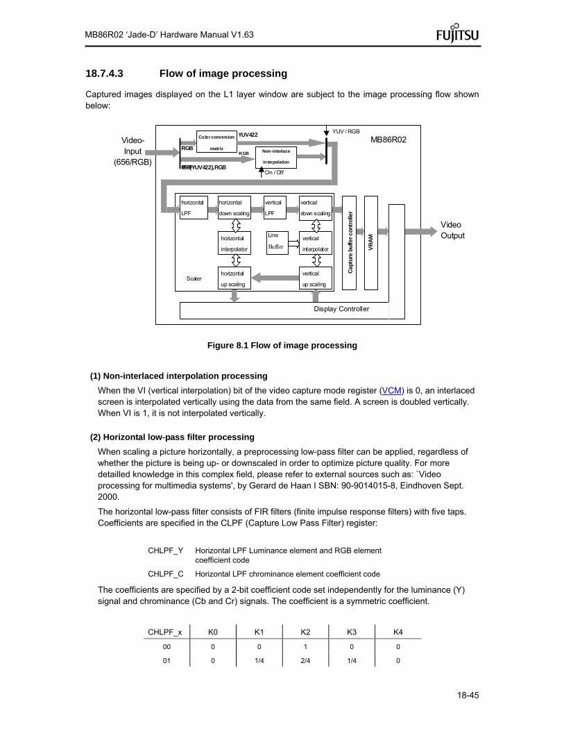
18-45
MB86R02 ‘Jade-D’ Hardware Manual V1.63
18.7.4.3 Flow of image processing
Captured images displayed on the L1 layer window are subject to the image processing flow shown below:
Figure 8.1 Flow of image processing
(1) Non-interlaced interpolation processing
When the VI (vertical interpolation) bit of the video capture mode register (VCM) is 0, an interlaced screen is interpolated vertically using the data from the same field. A screen is doubled vertically. When VI is 1, it is not interpolated vertically.
(2) Horizontal low-pass filter processing
When scaling a picture horizontally, a preprocessing low-pass filter can be applied, regardless of whether the picture is being up- or downscaled in order to optimize picture quality. For more detailled knowledge in this complex field, please refer to external sources such as: `Video processing for multimedia systems', by Gerard de Haan I SBN: 90-9014015-8, Eindhoven Sept. 2000.
The horizontal low-pass filter consists of FIR filters (finite impulse response filters) with five taps. Coefficients are specified in the CLPF (Capture Low Pass Filter) register:
CHLPF_Y Horizontal LPF Luminance element and RGB element coefficient code
CHLPF_C Horizontal LPF chrominance element coefficient code
The coefficients are specified by a 2-bit coefficient code set independently for the luminance (Y) signal and chrominance (Cb and Cr) signals. The coefficient is a symmetric coefficient.
CHLPF_x K0 K1 K2 K3 K4
00 0 0 1 0 0
01 0 1/4 2/4 1/4 0
Scaler
Video- Input
(656/RGB)
Video Output
MB86R02
horizontal
LPF horizontal
down scaling
vertical
down scaling
vertical
LPF
horizontal
up scaling
Display Controller
Non-interlace
interpolation
On / Off
Cap
ture
bu
ffe
r co
ntro
ller
VR
AM
Color conversion
matrix
656(YUV422),RGB
RGB
RGB
YUV422
RGB
YUV / RGB
vertical
up scaling
vertical
interpolator
horizontal
interpolator
Line
Buffer

18-46
MB86R02 ‘Jade-D’ Hardware Manual V1.63
10 0 3/16 10/16 3/16 0
11 3/32 8/32 10/32 10/32 3/32
The Horizontal LPF is deactivated (set to bypass) by setting the coefficient code to "00".
Note: In the case of Native RGB mode (NRGB=1), only a setup of CHLPF_Y code becomes effective.
(3) Horizontal Downscale and Upscale processing
Bits 15:0 of the capture scale register (CSC) are used for both horizontal downscale and upscale processing.
The horizontal downscaling of an incoming data stream is done before writing to VRAM. Upscaling in the horizontal direction is done after reading from VRAM.
The interpolation filter processing of the luminance (Y) signal is done using cubic interpolation (Cubic Interpolate) method. The interpolation filter processing of chrominance (Cb and Cr) signal is done using bilinear interpolation (BiLinear Interpolate) method. The interpolation filter processing of a Native-RGB signal is done by cubic interpolation (Cubic Interpolate) method.
(4) Vertical low-pass filter processing
A preprocessing vertical low-pass filter can be applied to an image before it is scaled down vertically. The vertical LPF can be activated, regardless of whether an image is scaled up or down in the vertical axis.
The vertical low-pass filter consists of FIR filters (finite impulse response filters) with three taps. Coefficients are specified in the CLPF (Capture Low Pass Filter) register:
CVLPF_Y Vertical LPF Luminance element and RGB element coefficient code
CVLPF_C Vertical LPF chrominance element coefficient code
The coefficients are specified by a 2-bit coefficient code set independently for the luminance (Y) signal and chrominance (Cb and Cr) signals. The coefficient is a symmetric coefficient.
18-47
MB86R02 ‘Jade-D’ Hardware Manual V1.63
CVLPF_x K0 K1 K2
00 0 1 0
01 1/4 2/4 1/4
10 3/16 10/16 3/16
11 Prohibition of setting
The Vertical LPF is deactivated (set to bypass) by setting the coefficient code to "00".
Note: In the case of Native RGB mode (NRGB=1), only a setup of CVLPF_Y code becomes effective.
(5) Vertical Upscaling and Downscaling processing
Bits 31:16 of the capture scale register (CSC) are used for both vertical downscale and upscale processing.
The vertical downscaling of an incoming data stream is done before writing to VRAM. Upscaling in the vertical direction is done after reading from VRAM.
The interpolation filter processing of the luminance (Y) signal is done using cubic interpolation (Cubic Interpolate) method. The interpolation filter processing of chrominance (Cb and Cr) signal is done using bilinear interpolation (BiLinear Interpolate) method. The interpolation filter processing of a Native-RGB signal is done by cubic interpolation (Cubic Interpolate) method.
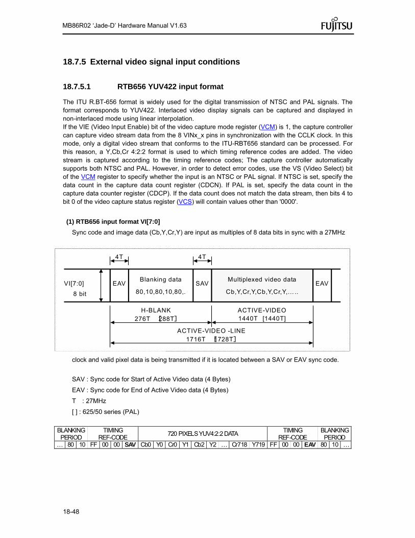
18-48
MB86R02 ‘Jade-D’ Hardware Manual V1.63
18.7.5 External video signal input conditions
18.7.5.1 RTB656 YUV422 input format
The ITU R.BT-656 format is widely used for the digital transmission of NTSC and PAL signals. The format corresponds to YUV422. Interlaced video display signals can be captured and displayed in non-interlaced mode using linear interpolation. If the VIE (Video Input Enable) bit of the video capture mode register (VCM) is 1, the capture controller can capture video stream data from the 8 VINx_x pins in synchronization with the CCLK clock. In this mode, only a digital video stream that conforms to the ITU-RBT656 standard can be processed. For this reason, a Y,Cb,Cr 4:2:2 format is used to which timing reference codes are added. The video stream is captured according to the timing reference codes; The capture controller automatically supports both NTSC and PAL. However, in order to detect error codes, use the VS (Video Select) bit of the VCM register to specify whether the input is an NTSC or PAL signal. If NTSC is set, specify the data count in the capture data count register (CDCN). If PAL is set, specify the data count in the capture data counter register (CDCP). If the data count does not match the data stream, then bits 4 to bit 0 of the video capture status register (VCS) will contain values other than '0000'.
(1) RTB656 input format VI[7:0]
Sync code and image data (Cb,Y,Cr,Y) are input as multiples of 8 data bits in sync with a 27MHz
clock and valid pixel data is being transmitted if it is located between a SAV or EAV sync code.
SAV : Sync code for Start of Active Video data (4 Bytes)
EAV : Sync code for End of Active Video data (4 Bytes)
T : 27MHz
[ ] : 625/50 series (PAL)
SAVEAV Multiplexed video data
Cb,Y,Cr,Y,Cb,Y,Cr,Y,….. 8 bit
VI[7:0]
4T
H-BLANK 276T 288T
ACTIVE-VIDEO1440T [1440T]
EAV
4T
Blanking data
80,10,80,10,80,.
ACTIVE-VIDEO -LINE 1716T 1728T
BLANKING PERIOD
TIMING REF-CODE
720 PIXELS YUV4:2:2 DATA TIMING REF-CODE
BLANKINGPERIOD
… 80 10 FF 00 00 SAV Cb0 Y0 Cr0 Y1 Cb2 Y2 … Cr718 Y719 FF 00 00 EAV 80 10 …

18-49
MB86R02 ‘Jade-D’ Hardware Manual V1.63
(2) RTB656 synchronous code (4 Byte) format
Word
Bit
SYNC code (static) EAV/SAV
first second third forth
7 1 0 0 1 (static)
6 1 0 0 F 0:first field 1:second field
5 1 0 0 V 0:ACTIVE-VIDEO 1:VBI
4 1 0 0 H 0:SAV 1:EAV
3 1 0 0 P3 Guard bit
2 1 0 0 P2 Guard bit
1 1 0 0 P1 Guard bit
0 1 0 0 P0 Guard bit
(3) SAV/EAV timing base signal
Bit 7 6 5 4 3 2 1 0
Function static F V H P3 P2 P1 P0
80 1 0 0 0 0 0 0 0
9D 1 0 0 1 1 1 0 1
AB 1 0 1 0 1 0 1 1
B6 1 0 1 1 0 1 1 0
C7 1 1 0 0 0 1 1 1
DA 1 1 0 1 1 0 1 0
EC 1 1 1 0 1 1 0 0
F1 1 1 1 1 0 0 0 1
80 : SAV code of first field valid pixel period (active video)
9D : EAV code of first field valid pixel period (active video)
AB : SAV code of first field vertical retrace line period
B6 : EAV code of first field vertical retrace line period
C7 : SAV code of second field valid pixel period (active video)
DA : EAV code of second field valid pixel period (active video)
EC : SAV code of second field vertical retrace line period
F1 : EAV code of second field vertical retrace line period

18-50
MB86R02 ‘Jade-D’ Hardware Manual V1.63
18.7.5.2 RGB input format
Two data processing methods exist for RGB input video capture functionality:
processing of Native RGB
processing by converting RGB into YUV422 using the internal RGB preprocessor.
The RGB input function is suitable for relatively fast, non-interlaced video signals but de-interlacing is not available in this mode. The maximum input rate is 66Mpixel/sec. Each RGB component is 6 bits wide.
Note: To use Native RGB mode, set the NRGB bit of the VCM register to '1'.
(1) RGB Input Signals
The RGB video capture input signals are not assigned to dedicated package pins. These pins are shared with other device functions (multiplexed, check MUX Group #5).
Name I/O Function
CCLK1 Input Clock for RGB input
RI1_7:RI1_2 Input Red component value
GI1_7:GI1_2 Input Green component value
BI1_7:BI1_2 Input Blue component value
VINVSYNC1 Input Vertical sync for RGB capture
HINVSYNC1 Input Horizontal sync for RGB capture
Note 1 : Input pins are shared with the ITU656 input and memory data bus. Note 2 : The VIS bit of the VCM (video capture mode) register selects which mode (RBT ITU656/601 or RGB) is used.
(2) Captured Range
In comparison to the embedded sync code method used in ITU656 input mode, the capture range in RGB mode is specified by register parameters, as shown below:
a) RGB input capture mode: Set the RGB666 input flag (VIS) in the VCM register.
For Native RGB mode, set NRGB=1 in the VCM register.
b) HSYNC Cycle: Set the number of HSYNC Cycles in RGBHC.
c) Horizontal Enable area: Set the area start position and picture size in RGBHST and RGBHEN.
d) Vertical Enable area: Set the area start position picture size in RGBVST and RGBVEN.
The capture area is defined according to the following parameters (each parameter is set independently in the respective register):
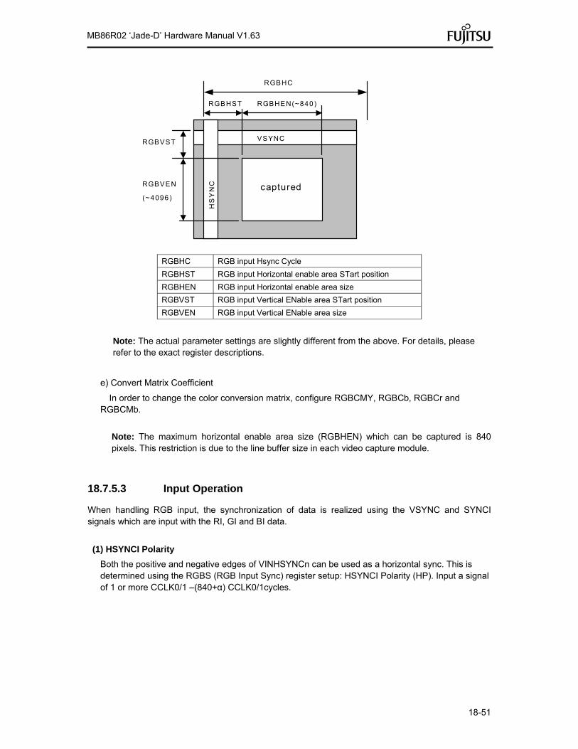
18-51
MB86R02 ‘Jade-D’ Hardware Manual V1.63
VSYNC
HS
YN
C
RGBHST
RGBVST
RGBHEN(~840)
RGBVEN
(~4096) captured
RGBHC
RGBHC RGB input Hsync Cycle
RGBHST RGB input Horizontal enable area STart position
RGBHEN RGB input Horizontal enable area size
RGBVST RGB input Vertical ENable area STart position
RGBVEN RGB input Vertical ENable area size
Note: The actual parameter settings are slightly different from the above. For details, please refer to the exact register descriptions.
e) Convert Matrix Coefficient
In order to change the color conversion matrix, configure RGBCMY, RGBCb, RGBCr and RGBCMb.
Note: The maximum horizontal enable area size (RGBHEN) which can be captured is 840 pixels. This restriction is due to the line buffer size in each video capture module.
18.7.5.3 Input Operation
When handling RGB input, the synchronization of data is realized using the VSYNC and SYNCI signals which are input with the RI, GI and BI data.
(1) HSYNCI Polarity
Both the positive and negative edges of VINHSYNCn can be used as a horizontal sync. This is determined using the RGBS (RGB Input Sync) register setup: HSYNCI Polarity (HP). Input a signal of 1 or more CCLK0/1 –(840+α) CCLK0/1cycles.
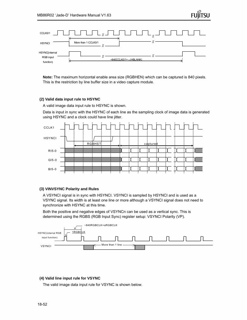
18-52
MB86R02 ‘Jade-D’ Hardware Manual V1.63
CCLK0/1
HSYNCI ∬
~840CCLK0/1+α(HBLANK)
More than 1 CCLK0/1 ∬
∬∬
HSYNC(internal
RGB input
function)
∬ ∬
Note: The maximum horizontal enable area size (RGBHEN) which can be captured is 840 pixels. This is the restriction by line buffer size in a video capture module.
(2) Valid data input rule to HSYNC
A valid image data input rule to HSYNC is shown.
Data is input in sync with the HSYNC of each line as the sampling clock of image data is generated using HSYNC and a clock could have line jitter.
CCLK1
HSY NCI
RI5-0
GI5-0
BI5-0
RGBHS T captured
(3) VINVSYNC Polarity and Rules
A VSYNCI signal is in sync with HSYNCI. VSYNCI is sampled by HSYNCI and is used as a VSYNC signal. Its width is at least one line or more although a VSYNCI signal does not need to synchronize with HSYNC at this time.
Both the positive and negative edges of VSYNCn can be used as a vertical sync. This is determined using the RGBS (RGB Input Sync) register setup: VSYNCI Polarity (VP).
More than 1 line
1RGBCLK HSYNC(internal RGB
input function)
VSYNCI
~840RGBCLK+αRGBCLK
(4) Valid line input rule for VSYNC
The valid image data input rule for VSYNC is shown below.

18-53
MB86R02 ‘Jade-D’ Hardware Manual V1.63
VSYNCI
HSYNCI
start to capture RGBVST
18.7.5.4 Conversion Operation
RGB input data is converted to YCbCr using the following matrix operation :
Y = a11R + a12G + a13B + b1
Cb= a21R + a22G + a23B + b2 aij :10bit signed real (the lower 8 bits are the fraction)
Cr= a31R + a32G + a33B + b3 bi: 8bit unsigned integer
Note 1 : Registers can define each coefficient. Note 2 : Cb and Cr components are halved after this operation for the 4:2:2 format.
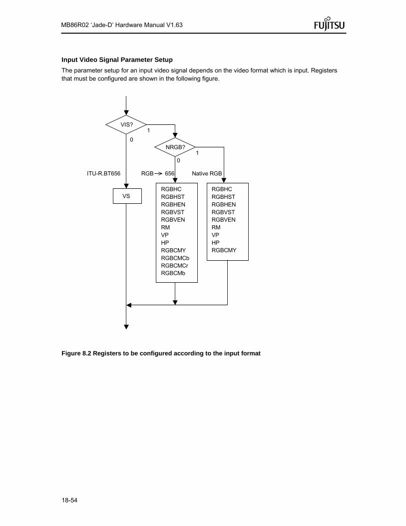
18-54
MB86R02 ‘Jade-D’ Hardware Manual V1.63
Input Video Signal Parameter Setup
The parameter setup for an input video signal depends on the video format which is input. Registers that must be configured are shown in the following figure.
VIS?
RGBHC RGBHST RGBHEN RGBVST RGBVEN RM VP HP RGBCMY RGBCMCbRGBCMCrRGBCMb
RGBHC RGBHST RGBHEN RGBVST RGBVEN RM VP HP RGBCMY
VS
ITU-R.BT656
NRGB?
Native RGB
0
1
01
RGB 656
Figure 8.2 Registers to be configured according to the input format

18-55
MB86R02 ‘Jade-D’ Hardware Manual V1.63
18.7.6 Display Controller / Video Capture Register Summary
18.7.6.1 Common Control Registers
A single register is used to control the main functionality of the display controllers/video capture units. BaseAddress = DisplayBase0 (=0xF1FD_0000)
Offset 31 30 29 28 27 26 25 24 23 22 21 20 19 18 17 16 15 14 13 12 11 10 9 8 7 6 5 4 3 2 1 0
7FF8
VCCC (Video/Capture Common Control)
dis2
s
hmon
mb
us
A1s
el
A0s
el
C1s
el
C0s
el
C1s
r
C0s
r
V1s
r
V0s
r
7FFC VCSR (Video/Capture Soft Reset)
18.7.6.2 Display Controller Registers
DisplayBaseAddress = DisplayBase0 (=0xF1FD_0000) or DisplayBase1 (=0xF1FD_2000)
Offset 31 30 29 28 27 26 25 24 23 22 21 20 19 18 17 16 15 14 13 12 11 10 9 8 7 6 5 4 3 2 1 0
000 DCM0 (Display Control Mode 0)
DE
N
L45E
L23E
L1E
L0E
CK
S
LCS
SC EE
Q
ED
E
EO
F
EO
D
SF
ES
Y
SYNC
100
DCM1 (Display Control Mode 1)
DE
N
L5E
L4E
L3E
L2E
L1E
L0E
CK
S
LCS
SC
EE
Q
ED
E
EO
F
EO
D
SF
ES
Y
SYNC
104 DCM2 (Display Control Mode 2)
RU
M1
R
UF
RU
M0
108
DCM3 (Display Control Mode 3)
pixb
uf
HS
Ydl
y
GV
D
VP
WM
s
CS
Y0
RG
Brv
RG
Bsh
MB
ST
RS
DS
PO
M
CK
ddr
CK
inv
CK
De
CKDn
004 HTP (H Total Pixels)
008 HDB (H Display Boundary) HDP (H Display Period)
00C
VS
WH
VSW HSW HSP (H Sync pulse Position)
010 VTR (V Total Rasters)
014 VDP (V Display Period) VSP (V Sync pulse Position)
018 WY (Window Y) WX (Window X)
01C WH (Window Height) WW (Window Width)

18-56
MB86R02 ‘Jade-D’ Hardware Manual V1.63
Offset 31 30 29 28 27 26 25 24 23 22 21 20 19 18 17 16 15 14 13 12 11 10 9 8 7 6 5 4 3 2 1 0
020 L0M (L0 Mode)
L0C
L0S (L0 Stride) L0H (L0 Height)
024 L0OA (L0 Origin Address)
028 L0DA (L0 Display Address)
02C L0DY (L0 Display Y) L0DX (L0 Display X)
110 L0EM (L0 Extend Mode)
L0EC L0PB
L0W
P
114 L0WY (L0 Window Y) L0WX (L0 Window X)
118 L0WH (L0 Window Height) L0WW (L0 Window Width)
030 L1M (L1 Mode)
L1C
L1Y
C
L1C
S
L1IM
L1S (L1 Stride)
034 L1OA0(L1 Origin Address 0) / CBDA0(Capure Buffer Display Address 0)
038 CBDA1 (Capture Buffer Display Address 1)
120 L1EM (L1 Extend Mode)
L1EC
L1C
P
VMAG L1PB
124 L1WY (L1 Window Y) L1WX (L1 Window X)
128 L1WH (L1 Window Height) L1WW (L1 Window Width)
040 L2M (L2 Mode)
L2C
L2FLP
L2S (L2 Stride) L0H (L0 Height)
044 L2OA0 (L2 Origin Address 0)
048 L2DA0 (L2 Display Address 0)
04C L2OA1 (L2 Origin Address 1)
050 L2DA1 (L2 Display Address 1)
054 L2DY (L2 Display Y) L2DX (L2 Display X)
130 L2EM (L2 Extend Mode)
L2EC L2PB
L2O
M
L2W
P
134 L2WY (L2 Window Y) L2WX (L2 Window X)
138 L2WH (L2 Window Height) L2WW (L2 Window Width)
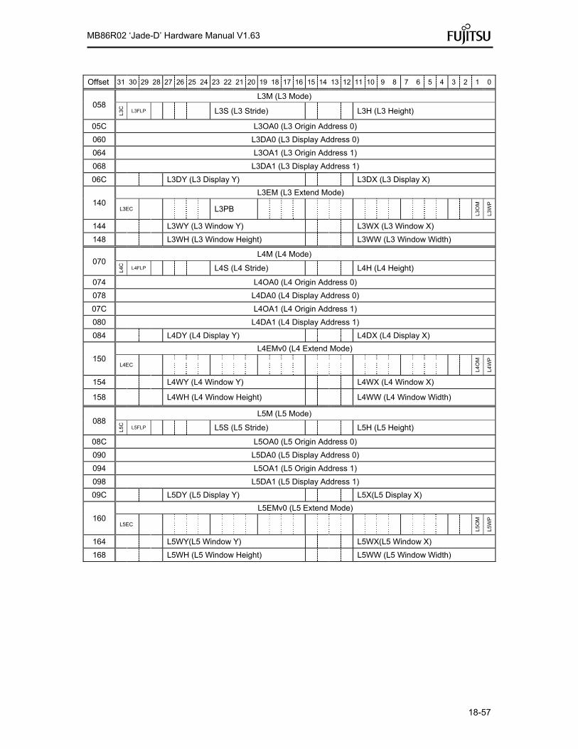
18-57
MB86R02 ‘Jade-D’ Hardware Manual V1.63
Offset 31 30 29 28 27 26 25 24 23 22 21 20 19 18 17 16 15 14 13 12 11 10 9 8 7 6 5 4 3 2 1 0
058 L3M (L3 Mode)
L3C
L3FLP
L3S (L3 Stride) L3H (L3 Height)
05C L3OA0 (L3 Origin Address 0)
060 L3DA0 (L3 Display Address 0)
064 L3OA1 (L3 Origin Address 1)
068 L3DA1 (L3 Display Address 1)
06C L3DY (L3 Display Y) L3DX (L3 Display X)
140 L3EM (L3 Extend Mode)
L3EC L3PB
L3O
M
L3W
P
144 L3WY (L3 Window Y) L3WX (L3 Window X)
148 L3WH (L3 Window Height) L3WW (L3 Window Width)
070 L4M (L4 Mode)
L4C
L4FLP
L4S (L4 Stride) L4H (L4 Height)
074 L4OA0 (L4 Origin Address 0)
078 L4DA0 (L4 Display Address 0)
07C L4OA1 (L4 Origin Address 1)
080 L4DA1 (L4 Display Address 1)
084 L4DY (L4 Display Y) L4DX (L4 Display X)
150 L4EMv0 (L4 Extend Mode)
L4EC
L4O
M
L4W
P
154 L4WY (L4 Window Y) L4WX (L4 Window X)
158 L4WH (L4 Window Height) L4WW (L4 Window Width)
088 L5M (L5 Mode)
L5C
L5FLP
L5S (L5 Stride) L5H (L5 Height)
08C L5OA0 (L5 Origin Address 0)
090 L5DA0 (L5 Display Address 0)
094 L5OA1 (L5 Origin Address 1)
098 L5DA1 (L5 Display Address 1)
09C L5DY (L5 Display Y) L5X(L5 Display X)
160 L5EMv0 (L5 Extend Mode)
L5EC
L5O
M
L5W
P
164 L5WY(L5 Window Y) L5WX(L5 Window X)
168 L5WH (L5 Window Height) L5WW (L5 Window Width)

18-58
MB86R02 ‘Jade-D’ Hardware Manual V1.63
Offset 31 30 29 28 27 26 25 24 23 22 21 20 19 18 17 16 15 14 13 12 11 10 9 8 7 6 5 4 3 2 1 0
0A0 CSIZE CPM CUTC (Cursor Transparent Control)
CSIZ1 CSIZ0
CU
E1
CU
E0
CU
O1
CU
O0
CU
ZT
CUTC
0A4 CUOA0 (CUrsor0 Origin Address)
0A8 CUY0 (Cursor0 Position Y) CUX0 (Cursor0 Position X)
0AC CUOA1 (CUrsor1 Origin Address)
0B0 CUY1 (Cursor1 Position Y) CUX1 (Cursor1 Position X)
170 MDC (Multi Display Control)
MD
EN
SC1EN SC0EN
180 DLS (Display Layer Select)
DLS5 DLS4 DLS3 DLS2 DLS1 DLS0
184 DBGC (Display Back Ground Color)
0B4 L0BLD (L0 Blend)
L0B
E
L0B
S
L0B
I
L0B
P
L0ID
res res L0BR
188 L1BLD (L1 Blend)
L1
BE
L1B
S
L1B
I
L1B
P
L1ID
res res L1BR
18C L2BLD (L2 Blend)
L2B
E
L2B
S
L2B
I
L2B
P
L2ID
res re
s L2BR
190 L3BLD (L3 Blend)
L3B
E
L3B
S
L3B
I
L3B
P
L3ID
res res L3BR
194 L4BLD (L4 Blend)
L4B
E
L4B
S
L4B
I
L4B
P
L4ID
res res L4BR
198 L5BLD (L5 Blend)
L5B
E
L5B
S
L5B
I
L5B
P
L5ID
res res L5BR

18-59
MB86R02 ‘Jade-D’ Hardware Manual V1.63
Offset 31 30 29 28 27 26 25 24 23 22 21 20 19 18 17 16 15 14 13 12 11 10 9 8 7 6 5 4 3 2 1 0
0BC L0TC (L0 Transparent Control)
L0Z
T
L0TC (L0 Transparent Color)
0C0 L2TR (L2 Transparent Control) L3TR (L3 Transparent Control)
L2Z
T
L2TC (L2 Transparent Color)
L0Z
T
L3TR (L3 Transparent Color)
1A0 L0TEC (L0 Extend Transparency Control)
L0E
ZT
L0ETC (L0 Extend Transparent Color)
1A4 L1TEC (L1 Transparent Extend Control)
L1E
ZT
L1ETC (L1 Extend Transparent Color)
1A8 L2TEC (L2 Transparent Extend Control)
L2E
ZT
L2ETC (L2 Extend Transparent Color)
1AC L3TEC (L3 Transparent Extend Control)
L0E
ZT
L3ETC (L3 Extend Transparent Color)
1B0 L4ETC (L4 Extend Transparent Control)
L4E
ZT
L4ETC (L4 Extend Transparent Color)
1B4 L5ETC (L5 Extend Transparent Control)
L5E
ZT
L5ETC (L5 Extend Transparent Color)
1E0 L1YCR0 (L1 YC to Red Coefficient 0)
a12 a11
1E4 L1YCR1 (L1 YC to Red Coefficient 1)
b1 a13
1E8 L1YCG0 (L1 YC to Green Coefficient 0)
a22 a21
1EC L1YCG1 (L1 YC to Green Coefficient 1)
b2 a23
1F0 L1YCB0 (L1 YC to Blue Coefficient 0)
a32 a31
1F4 L1YCB1 (L1 YC to Blue Coefficient 0)
b3 a33

18-60
MB86R02 ‘Jade-D’ Hardware Manual V1.63
Offset 31 30 29 28 27 26 25 24 23 22 21 20 19 18 17 16 15 14 13 12 11 10 9 8 7 6 5 4 3 2 1 0
400 L0PAL0
A R G B
404 L0PAL1
: :
7FC L0PAL255
800 L1PAL0
A R G B
804 L1PAL1
: :
BFC L1PAL255
1000 L2PAL0
A R G B
1004 L2PAL1
: :
13FC L2PAL255
1400 L3PAL0
A R G B
1404 L3PAL1
: :
17FC L3PAL255
1C00
VPWMM (Video PWM Mde)
EN
INV
VS
YR
HS
YR
EN
DR
HS
YB
1C04 VPWME (Video PWM End) VPWMS (Video PWM Start)
1C08
HO
LD
VPWMC (Video PWM Count)

18-61
MB86R02 ‘Jade-D’ Hardware Manual V1.63
18.7.6.3 Video capture registers
CaptureBaseAddress = CaptureBase0 (=0xF1FD_8000) or
CaptureBase1 (=0xF1FD_A000)
Offset 31 30 29 28 27 26 25 24 23 22 21 20 19 18 17 16 15 14 13 12 11 10 9 8 7 6 5 4 3 2 1 0
000
VCM (Video Capture Mode)
VIE
VIS
VIC
CM VI
NR
GB
VS
004 CSC (Capture SCale)
VSCI VSCF HSCI HSCF
008 VCS (Video Capture Status)
CE
010 CBM (Capture Buffer Mode)
OO
M
SB
UF
CR
GB
CBW (stride)
C24
CB
ST
014 CBOA (Capture Buffer Origin Address)
018 CBLA (Capture Buffer Limit Address)
01C CIVSTR CIHSTR
020 CIVEND CIHEND
028 CHP (Capture Horizontal Pixel)
CHP
02C CVP (Capture Vertical Pixel)
CVPP CVPN
048 CMSS (Capture Magnify Source Size)
CMSHP CMSVL
040 CLPF (Capture Low Pass Filter)
CVLPF CHLPF
04C CMDS (Capture Magnify Display Size)
CMDHP CMDVL
080 RGBHC (RGB input HSYNC Cycle)/VIN_HSSIZE
RGBHC
084 RGBHEN (RGB input Horizontal Enable Area)
RGBHST RGBHEN
088 RGBVEN (RGB input Vertical Enable Area)
RGBVST RGBVEN
090 RGBS (RGB input SYNC)
RM
HP
VP

18-62
MB86R02 ‘Jade-D’ Hardware Manual V1.63
Offset 31 30 29 28 27 26 25 24 23 22 21 20 19 18 17 16 15 14 13 12 11 10 9 8 7 6 5 4 3 2 1 0
0C0 RGBCMY (RGB Color convert Matrix Y coefficient)
a11 a12 a13
0C4 RGBCMCb (RGB Color convert Matrix Cb coefficient)
a21 a22 a23
0C8 RGBCMCr (RGB Color convert Matrix Cr coefficient)
a31 a32 a33
0CC RGBCMb (RGB Color convert Matrix b coefficient)
b1 b2 b3
4000 CDCN (Capture Data Count for NTSC)
BDCN VDCN
4004 CDCP (Capture Data Count for PAL)
BDCP VDCP

18-63
MB86R02 ‘Jade-D’ Hardware Manual V1.63
18.7.7 Explanation of Local Memory Registers
Terms appeared in this chapter are explained below: 1. Register address Indicates address of register 2. Bit number Indicates bit number 3. Bit field name Indicates name of each bit field included in register 4. R/W Indicates access attribute (read/write) of each field Each symbol shown in this section denotes the following:
R0 “0” always read at read. Write access is Don’t care.
W0 Only “0” can be written.
R Read enabled
W Write enabled
RX Read enabled (read values undefined)
RW Read and write enabled
RW0 Read and write 0 enabled 5. Initial value
Indicates initial value of immediately before the reset of each bit field. “X“ means no deterministic value
6. Handling of reserved bits
“0” is recommended for the write value so that compatibility can be maintained with future products.
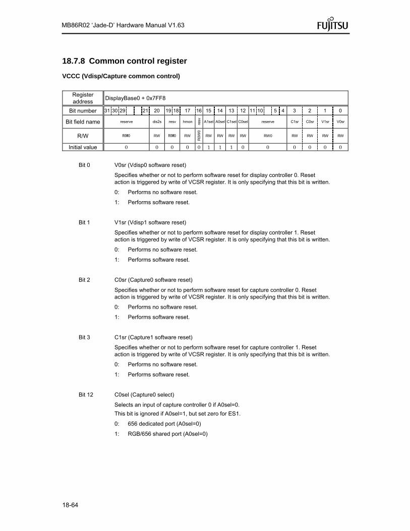
18-64
MB86R02 ‘Jade-D’ Hardware Manual V1.63
18.7.8 Common control register
VCCC (Vdisp/Capture common control)
Register address
DisplayBase0 + 0x7FF8
Bit number 31 30 29 21 20 19 18 17 16 15 14 13 12 11 10 5 4 3 2 1 0
Bit field name reserve dis2s resv hmon resv
A1sel A0sel C1sel C0sel reserve C1sr C0sr V1sr V0sr
R/W R0W0 RW R0W0 RW
R0W
0
RW RW RW RW RW0 RW RW RW RW
Initial value 0 0 0 0 0 1 1 1 0 0 0 0 0 0
Bit 0 V0sr (Vdisp0 software reset)
Specifies whether or not to perform software reset for display controller 0. Reset action is triggered by write of VCSR register. It is only specifying that this bit is written.
0: Performs no software reset.
1: Performs software reset.
Bit 1 V1sr (Vdisp1 software reset)
Specifies whether or not to perform software reset for display controller 1. Reset action is triggered by write of VCSR register. It is only specifying that this bit is written.
0: Performs no software reset.
1: Performs software reset.
Bit 2 C0sr (Capture0 software reset)
Specifies whether or not to perform software reset for capture controller 0. Reset action is triggered by write of VCSR register. It is only specifying that this bit is written.
0: Performs no software reset.
1: Performs software reset.
Bit 3 C1sr (Capture1 software reset)
Specifies whether or not to perform software reset for capture controller 1. Reset action is triggered by write of VCSR register. It is only specifying that this bit is written.
0: Performs no software reset.
1: Performs software reset.
Bit 12 C0sel (Capture0 select)
Selects an input of capture controller 0 if A0sel=0.
This bit is ignored if A0sel=1, but set zero for ES1.
0: 656 dedicated port (A0sel=0)
1: RGB/656 shared port (A0sel=0)

18-65
MB86R02 ‘Jade-D’ Hardware Manual V1.63
Bit 13 C1sel (Capture1 select)
Selects an input of capture controller 1.
This bit is ignored if A1sel=1, but set one for ES1.
0: 656 dedicated port (A1sel=0)
1: RGB/656 shared port (A1sel=0)
Bit 14 A0sel (Apix capture 0 select)
Selects Apix input for capture controller 0.
0: 656 dedicated port
1: Apix ch 0
Bit 15 A1sel (Apix capture 1 select)
Selects Apix input for capture controller 1.
0: RGB/656 shared port
1: Apix ch 1
Bit 17 hmon (host monitor)
This specifies a debug function that displays data access of host CPU on screen.
Upper hexadecimal value means address and lower one means data.
0: disable
1: enable
Bit 20 dis2s (display two select)
Specifies use of internal demultiplexer for multiplex dual display mode
0: Two video outputs are connected to two display controllers, respectively
1: Two video outputs are connected to internal demultiplexer of display controller 0

18-66
MB86R02 ‘Jade-D’ Hardware Manual V1.63
18.7.9 Display control register
DCM0/1 (Display Control Mode 0/1) Register address
DisplayBaseAddress + 0x00 (DCM0)
Bit number 31 30 29 28 27 26 25 24 23 22 21 20 19 18 17 16 15 14 13 12 11 10 9 8 7 6 5 4 3 2 1 0
Bit field name DE
N
ST
OP
Reserve
L45E
L23E
L1E
L0E
CK
S
Resv SC
EE
Q
OD
E
Res
v
Res
v
SF
ES
Y
SYNC
R/W RW RW RX RW RW RW RW RW R0 RW RW RW RW R0 RW RW RW
Initial value 0 0 0 0 0 0 0 0 1110 0 0 0 0 0 0 00
Register address
DisplayBaseAddress + 0x100 (DCM1)
Bit number 31 30 29 28 27 26 25 24 23 22 21 20 19 18 17 16 15 14 13 12 11 10 9 8 7 6 5 4 3 2 1 0
Bit field name DE
N
ST
OP
Reserve L5E
L4E
L3E
L2E
L1E
L0E
CK
S
LCS
SC
EE
Q
OD
E
Res
v
Res
v
SF
ES
Y
SYNC
R/W RW RW RX RW RW RW RW RW RW RW RW RW RW RW RW R0 RW RW RW
Initial value 0 0 X 0 0 0 0 0 0 0 0 11101 0 0 0 0 0 0 00
This register controls the display count mode. It is not initialized by a software reset. This register is mapped to two addresses but it is one substance. The differences between the two registers are the format of the frequency division rate setting (SC) and layer enable. The two formats exist to maintain backword compatibility with previous products.
Bit 1 to 0 SYNC (Synchronize)
Set synchronization mode
X0 Non-interlace mode
10 Interlace mode
11 Interlace video mode
Bit 2 ESY (External Synchronize)
Sets external synchronization mode
0: External synchronization disabled
1: External synchronization enabled
Bit 3 SF (Synchronize signal format)
Sets format of synchronization (VSYNC, HSYNC) signals
0: Negative logic
1: Positive logic
Bit 6 ODE
Odd/Even detect (TBD)
Bit 7 EEQ (Enable Equalizing pulse)
Sets CCYNC signal mode

18-67
MB86R02 ‘Jade-D’ Hardware Manual V1.63
0: Does not insert equalizing pulse into CCYNC signal
1: Inserts equalizing pulse into CCYNC signal
Bit 13 to 8 SC (Scaling)
Divides display reference clock by the preset ratio to generate dot clock
Offset 0 Offset 100H
x00000 Frequency not divided 000000 Frequency not divided
x00001 Frequency division rate = 1/4 000001 Frequency division rate = 1/2
x00010 Frequency division rate = 1/6 000010 Frequency division rate = 1/3
X00011 Frequency division rate = 1/8 000011 Frequency division rate = 1/4
: :
x11111 Frequency division rate = 1/64 111111 Frequency division rate = 1/64
When n is set, with Offset = 0, the frequency division rate is 1/(2n + 2).
When m is set, with Offset = 100h, the frequency division rate is 1/(m + 1).
Basically, these are setting parameters with the same function (2n + 2 = m + 1). Because of this, m = 2n + 1 is established. When n is set to the SC field with Offset = 0, 2n + 1 is reflected with Offset = 100h.
Also, when PLL is selected as the reference clock, frequency division rates 1/1 to 1/5 are non-functional even when set; other frequency division rates are assigned.
Bit 14 LCS (Lower Frequency Clock Select)
Predivide the clock signal for the dot clock
0: The clock source for the scaler is the internal PLL clock.
1: The clock source for the scaler is 1/4 of the frequency of the internal PLL clock. This can be used to generate lower dot clock frequencies.
LCS=0 => Dot clock = (PLL clock)/(scaler)
LCS=1 => Dot clock = (PLL clock)/(scaler)/4
Bit 15 CKS (Clock Source)
Selects reference clock
0: Internal PLL output clock
1: DCLKI input
Bit 16 L0E (L0 layer Enable)
Enables display of the L0 layer. The L0 layer corresponds to the C layer for previous products.
0: Does not display L0 layer
1: Displays L0 layer
Bit 17 L1E (L1 layer Enable)
Enables display of the L1 layer. The L1 layer corresponds to the W layer for previous products.
0: Does not display L1 layer
1: Displays L1 layer
Bit 18 L23E (L2 & L3 layer Enable) ------ DCM0

18-68
MB86R02 ‘Jade-D’ Hardware Manual V1.63
Enables simultaneous display of the L2 and L3 layers. These layers correspond to the M layer for previous products.
0: Does not display L2 and L3 layer
1: Displays L2 and L3 layer
L2E (L2 layer Enable) ------ DCM1
Enables L2 layer display
0: Does not display L2 layer
1: Displays L2 layer
Bit 19 L45E (L4 & L5 layer Enable) ------ DCM0
Enables simultaneous display of the L4 and L5 layers. These layers correspond to the B layer for previous products.
0: Does not display L4 and L5 layer
1: Displays L4 and L5 layer
L3E (L3 layer Enable)) ------ DCM1
Enables L3 layer display
0: Does not display L3 layer
1: Displays L3 layer
Bit 20 L4E (L4 layer Enable)
Enables L4 layer display
0: Does not display L4 layer
1: Displays L4 layer
Bit 21 L5E (L5 layer Enable)
Enables L5 layer display
0: Does not display L5 layer
1: Displays L5 layer
Bit 30 STOP
(TBD)
Bit 31 DEN (Display Enable)
Enables display
0: Does not output display signal
1: Outputs display signal
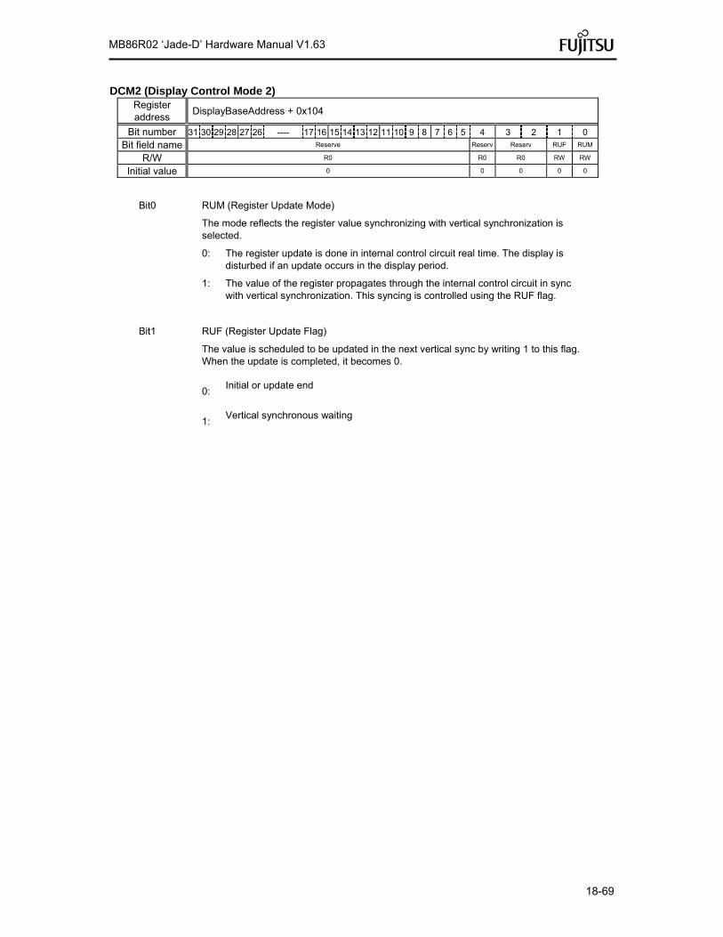
18-69
MB86R02 ‘Jade-D’ Hardware Manual V1.63
DCM2 (Display Control Mode 2) Register address
DisplayBaseAddress + 0x104
Bit number 31 30 29 28 27 26 ---- 17 16 15 14 13 12 11 10 9 8 7 6 5 4 3 2 1 0
Bit field name Reserve Reserv Reserv RUF RUM
R/W R0 R0 R0 RW RW
Initial value 0 0 0 0 0
Bit0 RUM (Register Update Mode)
The mode reflects the register value synchronizing with vertical synchronization is selected.
0: The register update is done in internal control circuit real time. The display is disturbed if an update occurs in the display period.
1: The value of the register propagates through the internal control circuit in sync with vertical synchronization. This syncing is controlled using the RUF flag.
Bit1 RUF (Register Update Flag)
The value is scheduled to be updated in the next vertical sync by writing 1 to this flag. When the update is completed, it becomes 0.
0:
Initial or update end
1:
Vertical synchronous waiting
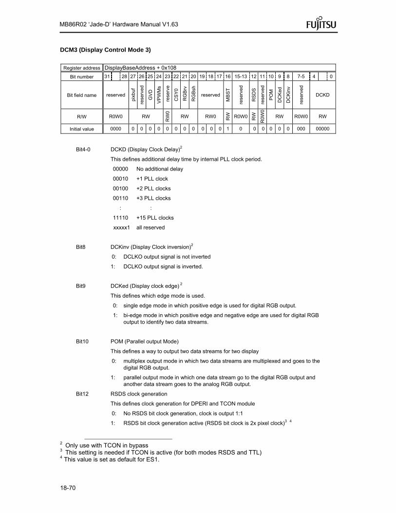
18-70
MB86R02 ‘Jade-D’ Hardware Manual V1.63
DCM3 (Display Control Mode 3)
Register address DisplayBaseAddress + 0x108
Bit number 31 28 27 26 25 24 23 22 21 20 19 18 17 16 15-13 12 11 10 9 8 7-5 4 0
Bit field name reserved
pix
buf
rese
rve
d
GV
D
VP
WM
s
re
serv
e
CS
Y0
RG
Brv
RG
Bsh
reserved
MB
ST
rese
rve
d
RS
DS
rese
rve
d
PO
M
DC
Ked
DC
Kin
v
rese
rve
d
DCKD
R/W R0W0 RW
RW
0
RW RW0 RW
R0W0 RW
R0W
0
RW R0W0 RW
Initial value 0000 0 0 0 0 0 0 0 0 0 0 0 1 0 0 0 0 0 0 000 00000
Bit4-0 DCKD (Display Clock Delay)2
This defines additional delay time by internal PLL clock period.
00000 No additional delay
00010 +1 PLL clock
00100 +2 PLL clocks
00110 +3 PLL clocks
: :
11110 +15 PLL clocks
xxxxx1 all reserved
Bit8 DCKinv (Display Clock inversion)2
0: DCLKO output signal is not inverted
1: DCLKO output signal is inverted.
Bit9 DCKed (Display clock edge) 2
This defines which edge mode is used.
0: single edge mode in which positive edge is used for digital RGB output.
1: bi-edge mode in which positive edge and negative edge are used for digital RGB
output to identify two data streams.
Bit10 POM (Parallel output Mode)
This defines a way to output two data streams for two display
0: multiplex output mode in which two data streams are multiplexed and goes to the
digital RGB output.
1: parallel output mode in which one data stream go to the digital RGB output and
another data stream goes to the analog RGB output.
Bit12 RSDS clock generation
This defines clock generation for DPERI and TCON module
0: No RSDS bit clock generation, clock is output 1:1
1: RSDS bit clock generation active (RSDS bit clock is 2x pixel clock)3 4
2 Only use with TCON in bypass 3 This setting is needed if TCON is active (for both modes RSDS and TTL) 4 This value is set as default for ES1.

18-71
MB86R02 ‘Jade-D’ Hardware Manual V1.63
Bit31 – 13 Reserved, do not modify
Bit16 MBST (Memory Bust )
This bit selects SDRAM burst length. In general, 32word burst is more efficient.
0: SDRAM burst length is 16word ( 1word=32bit)
1: SDRAM burst length is 32word ( 1word=32bit)
Bit20 RGBsh ( RGB output shift)
This function is intended for debugging purposes
0: no shift
1: shitft RGB output to LSB by 2bit
Bit21 RGBrv ( RGB output reverse)
This function is intended for debugging purposes
0: no reverse
1: reverse bit order of RGB output
Bit22 CSY0 ( CSYNC output zero)
If CSYNC output is connected to external DAC input for sync-on-green, this bit can be used as sync-on-green disable.
0: CSYNC singal is valid
1: CSYNC signal is fixed to zero therefore sync-on-green is disabled. Refer to the specification of the connected DAC
Bit24 VPWMs ( Video sync PWM select)
0: Disable VPWM signal and select GV signal for GV/VPWM output
1: Disable GV signal and select VPWM signal for GV/VPWM output
Bit25 GVD ( GV output delay)
0: no delay
1: one clock delay is given to GV output to compensate external DAC.

18-72
MB86R02 ‘Jade-D’ Hardware Manual V1.63
HTP (Horizontal Total Pixels) Register address
DisplayBaseAddress + 0x06
Bit number 15 14 13 12 11 10 9 8 7 6 5 4 3 2 1 0
Bit field name Reserved HTP
R/W R0 RW
Initial value 0 X
This register controls the horizontal total pixel count. Setting value + 1 is the total pixel count.
HDP (Horizontal Display Period) Register address
DisplayBaseAddress + 0x08
Bit number 15 14 13 12 11 10 9 8 7 6 5 4 3 2 1 0
Bit field name Reserved HDP
R/W R0 RW
Initial value 0 X
This register controls the total horizontal display period in unit of pixel clocks. Setting value + 1 is the pixel count for the display period.
HDB (Horizontal Display Boundary) Register address
DisplayBaseAddress + 0x0A
Bit number 15 14 13 12 11 10 9 8 7 6 5 4 3 2 1 0
Bit field name Reserved HDB
R/W R0 RW
Initial value 0 X
This register controls the display period of the left part of the window in unit of pixel clocks. Setting value + 1 is the pixel count for the display period of the left part of the window. When the window is not divided into right and left before display, set the same value as HDP.
HSP (Horizontal Synchronize pulse Position) Register address
DisplayBaseAddress + 0x0C
Bit number 15 14 13 12 11 10 9 8 7 6 5 4 3 2 1 0
Bit field name Reserved HSP
R/W R0 RW
Initial value 0 X
This register controls the pulse position of the horizontal synchronization signal in unit of pixel clocks. When the clock count since the start of the display period reaches setting value + 1, the horizontal synchronization signal is asserted.
HSW (Horizontal Synchronize pulse Width) Register address
DisplayBaseAddress + 0x0E
Bit number 7 6 5 4 3 2 1 0
Bit field name HSW
R/W RW
Initial value X
This register controls the pulse width of the horizontal synchronization signal in unit of pixel clocks. Setting value + 1 is the pulse width clock count.

18-73
MB86R02 ‘Jade-D’ Hardware Manual V1.63
VSW (Vertical Synchronize pulse Width) Register address
DisplayBaseAddress + 0x0F
Bit number 7 6 5 4 3 2 1 0
Bit field name Reserved VSW
R/W R0 RW
Initial value 0 X
This register controls the pulse width of vertical synchronization signal in unit of raster. Setting value + 1 is the pulse width raster count.
VTR (Vertical Total Rasters) Register address
DisplayBaseAddress + 0x12
Bit number 15 14 13 12 11 10 9 8 7 6 5 4 3 2 1 0
Bit field name Reserved VTR
R/W R0 RW
Initial value 0 X
This register controls the vertical total raster count. Setting value + 1 is the total raster count. For the interlace display, Setting value + 1.5 is the total raster count for 1 field; 2 setting value + 3 is the total raster count for 1 frame (see Section 8.3.2).
VSP (Vertical Synchronize pulse Position) Register address
DisplayBaseAddress + 0x14
Bit number 15 14 13 12 11 10 9 8 7 6 5 4 3 2 1 0
Bit field name Reserved VSP
R/W R0 RW
Initial value 0 X
This register controls the pulse position of vertical synchronization signal in unit of raster. The vertical synchronization pulse is asserted starting at the setting value + 1st raster relative to the display start raster
.
VDP (Vertical Display Period) Register address
DisplayBaseAddress + 0x16
Bit number 15 14 13 12 11 10 9 8 7 6 5 4 3 2 1 0
Bit field name Reserved VDP
R/W R0 RW
Initial value 0 X
This register controls the vertical display period in unit of raster. Setting value + 1 is the count of raster to be displayed.

18-74
MB86R02 ‘Jade-D’ Hardware Manual V1.63
L0M (L0 layer Mode)
Register address
DisplayBaseAddress + 0x20
Bit number 31 30 29 28 27 26 25 24 23 22 21 --- 17 16 15 14 13 12 11 10 9 8 ---- 2 1 0
Bit field name L0C Reserved Reserved L0W Reserved L0H
R/W RW R0 R0 RW R0 RW
Initial value 0 0 0 X 0 X
Bit 11 to 0 L0H (L0 layer Height)
Specifies the height of the logic frame of the L0 layer in pixel units. Setting value + 1 is the height
Bit 23 to 16 L0W (L0 layer memory Width)
Sets the memory width (stride) of the logic frame of the L0 layer in 64-byte units
Bit 31 L0C (L0 layer Color mode)
Sets the color mode for L0 layer
0 Indirect color (8 bits/pixel) mode ARGB
1 Direct color (16 bits/pixel) mode ARGB
L0EM (L0-layer Extended Mode) Register address
DisplayBaseAddress + 0x110
Bit number 31 30 29 28 27 26 25 24 23 22 21 20 19 18 17 16 15 14 13 12 11 10 ----- 4 3 2 1 0
Bit field name L0EC Reserved L0PB Reserved L0WP
R/W RW R0 RW R0 RW
Initial value 0 0 0
Bit 0 L0 WP (L0 layer Window Position enable)
Selects the display position of L0 layer
0 Compatibility mode display (C layer supported)
1 Window display
Bit 23 to 20 L0PB (L0 layer Palette Base)
Shows the value added to the index when subtracting palette of L0 layer. 16 times of setting value is added.
Bit 31 and 30 L0EC (L0 layer Extended Color mode)
Sets extended color mode for L0 layer
00 Mode determined by L0C (8/16 ARGB)
01 Direct color (24 bits/pixel) mode ARGB
10 16bpp RGBA
11 24 bpp RGBA
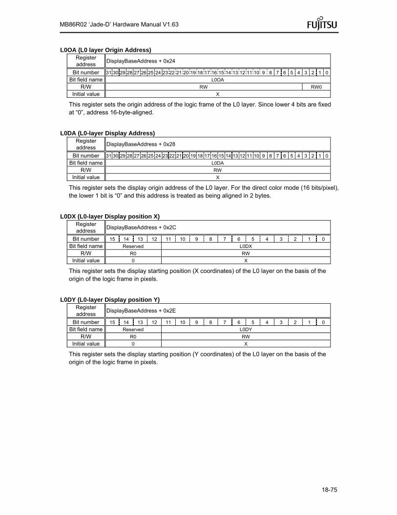
18-75
MB86R02 ‘Jade-D’ Hardware Manual V1.63
L0OA (L0 layer Origin Address) Register address
DisplayBaseAddress + 0x24
Bit number 31 30 29 28 27 26 25 24 23 22 21 20 19 18 17 16 15 14 13 12 11 10 9 8 7 6 5 4 3 2 1 0
Bit field name L0OA
R/W RW RW0
Initial value X
This register sets the origin address of the logic frame of the L0 layer. Since lower 4 bits are fixed at “0”, address 16-byte-aligned.
L0DA (L0-layer Display Address) Register address
DisplayBaseAddress + 0x28
Bit number 31 30 29 28 27 26 25 24 23 22 21 20 19 18 17 16 15 14 13 12 11 10 9 8 7 6 5 4 3 2 1 0
Bit field name L0DA
R/W RW
Initial value X
This register sets the display origin address of the L0 layer. For the direct color mode (16 bits/pixel), the lower 1 bit is “0” and this address is treated as being aligned in 2 bytes.
L0DX (L0-layer Display position X) Register address
DisplayBaseAddress + 0x2C
Bit number 15 14 13 12 11 10 9 8 7 6 5 4 3 2 1 0
Bit field name Reserved L0DX
R/W R0 RW
Initial value 0 X
This register sets the display starting position (X coordinates) of the L0 layer on the basis of the origin of the logic frame in pixels.
L0DY (L0-layer Display position Y) Register address
DisplayBaseAddress + 0x2E
Bit number 15 14 13 12 11 10 9 8 7 6 5 4 3 2 1 0
Bit field name Reserved L0DY
R/W R0 RW
Initial value 0 X
This register sets the display starting position (Y coordinates) of the L0 layer on the basis of the origin of the logic frame in pixels.

18-76
MB86R02 ‘Jade-D’ Hardware Manual V1.63
L0WX (L0 layer Window position X) Register address
DisplayBaseAddress + 0x114
Bit number 15 14 13 12 11 10 9 8 7 6 5 4 3 2 1 0
Bit field name Reserved L0WX
R/W R0 RW
Initial value 0 X
This register sets the X coordinates of the display position of the L0 layer window.
L0WY (L0 layer Window position Y) Register address
DisplayBaseAddress + 0x116
Bit number 15 14 13 12 11 10 9 8 7 6 5 4 3 2 1 0
Bit field name Reserved L0WY
R/W R0 RW
Initial value 0 X
This register sets the Y coordinates of the display position of the L0 layer window.
L0WW (L0 layer Window Width) Register address
DisplayBaseAddress + 0x118
Bit number 15 14 13 12 11 10 9 8 7 6 5 4 3 2 1 0
Bit field name Reserved L0WW
R/W R0 RW
Initial value 0 X
This register controls the horizontal direction display size (width) of the L0 layer window. Do not specify “0”.
L0WH (L0 layer Window Height) Register address
DisplayBaseAddress + 0x11A
Bit number 15 14 13 12 11 10 9 8 7 6 5 4 3 2 1 0
Bit field name Reserved L0WH
R/W R0 RW
Initial value 0 X
This register controls the vertical direction display size (height) of the L0 layer window. Setting value + 1 is the height.

18-77
MB86R02 ‘Jade-D’ Hardware Manual V1.63
L1M (L1-layer Mode) Register address
DisplayBaseAddress + 0x30
Bit number 31 30 29 28 27 26 25 24 23 22 21 20 19 18 17 16 15 14 13 12 11 10 --- 5 4 3 2 1 0
Bit field name L1C L1YC L1CS L1IM Reserved L1W Reserved
R/W
Initial value
Bit 23 to 16 L1W (L1 layer memory Width)
Sets the memory width (stride) of the logic frame of the W layer in unit of 64 bytes
Bit 28 L1IM (L1 layer Interlace Mode)
Sets video capture mode when L1CS in capture mode
0: Normal mode
1: For non-interlace display, displays captured video graphics in WEAVE mode
For interlace and video display, buffers are managed in frame units (pair of odd field and even field).
Bit 29 L1CS (L1 layer Capture Synchronize)
Sets whether the layer is used as normal display layer or as video capture
0: Normal mode
1: Capture mode
Bit 30 L1YC (L1 layer YC mode)
Sets color format of L1 layer
The YC mode must be set for video capture.
0: RGB mode
1: YC mode
Bit 31 L1C (L1 layer Color mode)
Sets color mode for L1 layer
0: Indirect color (8 bits/pixel) mode ARGB
1: Direct color (16 bits/pixel) mode ARGB

18-78
MB86R02 ‘Jade-D’ Hardware Manual V1.63
L1EM (L1 layer Extended Mode) Register address
DisplayBaseAddress + 0x120
Bit number 31 30 29 28 27 26 25 24 23 22 21 20 19 18 17 16 15 14 13 12 11 10 4 3 2 1 0
Bit field name L1EC Reserved DM L1PB Reserved
R/W RW R0 RW R0
Initial value 0 0
Bit 23 to 20 L1PB (L1 layer Palette Base)
Shows the value added to the index when subtracting palette of L1 layer. 16 times of setting value is added.
Bit 25 to 24 L1DM (L1 layer Display Magnify Mode)
00 Normal Mode (no scaling or shrink scaling)
01 Reserved
10 Magnify Scaling
11 Reserved
Bit 31 and 30 L1EC (L1 layer Extended Color mode)
Sets extended color mode for L1 layer
00 Mode determined by L1C (8/16 ARGB)
01 Direct color (24 bits/pixel) mode ARGB
10 16bpp RGBA
11 24 bpp RGBA
L1DA (L1 layer Display Address) Register address
DisplayBaseAddress + 0x34
Bit number 31 30 29 28 27 26 25 24 23 22 21 20 19 18 17 16 15 14 13 12 11 10 9 8 7 6 5 4 3 2 1 0
Bit field name Reserved L1DA
R/W R0 RW
Initial value 0 X
This register sets the display origin address of the L1 layer. For the direct color mode (16 bits/pixel), the lower 1 bit is “0” and this register is treated as being aligned in 2 bytes. Wraparound processing is not performed for the L1 layer, so the frame origin linear address and display position (X coordinates and Y coordinates) are not specified.
L1WX (L1 layer Window position X) Register address
DisplayBaseAddress + 0x124 (DisplayBaseAddress + 0x18)
Bit number 15 14 13 12 11 10 9 8 7 6 5 4 3 2 1 0
Bit field name Reserved L1WX
R/W R0 RW
Initial value 0 X
This register sets the X coordinates of the display position of the L1 layer window. This register is placed in two address spaces. The parenthesized address is the register address to maintain compatibility with previous products. The same applies to L1WY, L1WW and L1WH.

18-79
MB86R02 ‘Jade-D’ Hardware Manual V1.63
L1WY (L1 layer Window position Y) Register address
DisplayBaseAddress + 0x126 (DisplayBaseAddress + 0x1A)
Bit number 15 14 13 12 11 10 9 8 7 6 5 4 3 2 1 0
Bit field name Reserved L1WY
R/W R0 RW
Initial value 0 X
This register sets the Y coordinates of the display position of the L1 layer window.
L1WW (L1 layer Window Width) Register address
DisplayBaseAddress + 0x128 (DisplayBaseAddress + 0x1C)
Bit number 15 14 13 12 11 10 9 8 7 6 5 4 3 2 1 0
Bit field name Reserved L1WW
R/W R0 RW
Initial value 0 X
This register controls the horizontal direction display size (width) of the L1 layer window. Do not specify “0”.
L1WH (L1 layer Window Height) Register address
DisplayBaseAddress + 0x12A ((DisplayBaseAddress + 0x1E)
Bit number 15 14 13 12 11 10 9 8 7 6 5 4 3 2 1 0
Bit field name Reserved L1WH
R/W R0 RW
Initial value 0 X
This register controls the vertical direction display size (height) of the L1 layer window. Setting value + 1 is the height.

18-80
MB86R02 ‘Jade-D’ Hardware Manual V1.63
L2M (L2 layer Mode)
Register address
DisplayBaseAddress + 0x40
Bit number 31 30 29 28 27 26 25 24 23 22 21 --- 17 16 15 14 13 12 11 10 9 8 ---- 2 1 0
Bit field name L2C L2FLP Reserved L2W Reserved L2H
R/W RW RW R0 RW R0 RW
Initial value 0 0 0 X 0 X
Bit 11 to 0 L2H (L2 layer Height)
Specifies the height of the logic frame of the L2 layer in pixel units. Setting value + 1 is the height
Bit 23 to 16 L2W (L2 layer memory Width)
Sets the memory width (stride) of the logic frame of the L2 layer in 64-byte units
Bit 30 and 29 L2FLP (L2 layer Flip mode)
Sets flipping mode for L2 layer
00 Displays frame 0
01 Displays frame 1
10 Switches frame 0 and 1 alternately for display
11 Reserved
Bit 31 L2C (L2 layer Color mode)
Sets the color mode for L2 layer
0 Indirect color (8 bits/pixel) mode ARGB
1 Direct color (16 bits/pixel) mode ARGB

18-81
MB86R02 ‘Jade-D’ Hardware Manual V1.63
L2EM (L2 layer Extended Mode) Register address
DisplayBaseAddress + 0x130
Bit number 31 30 29 28 27 26 25 24 23 22 21 20 19 18 17 16 15 14 13 12 11 10 ----- 4 3 2 1 0
Bit field name L2EC Reserved L2PB Reserved L2OM L2WP
R/W RW R0 RW R0 RW RW
Initial value 00 0 0 0 0 0
Bit 0 L2 WP (L2 layer Window Position enable)
Selects the display position of L2 layer
0 Compatibility mode display (ML layer supported)
1 Window display
Bit 1 L2OM (L2 layer Overlay Mode)
Selects the overlay mode for L2 layer
0 Compatibility mode
1 Extended mode
Bit 23 to 20 L2PB (L2 layer Palette Base)
Shows the value added to the index when subtracting palette of L2 layer. 16 times of setting value is added.
Bit 31 and 30 L2EC (L2 layer Extended Color mode)
Sets extended color mode for L2 layer
00 Mode determined by L2C
01 Direct color (24 bits/pixel) mode
10 16bpp RGBA
11 24 bpp RGBA
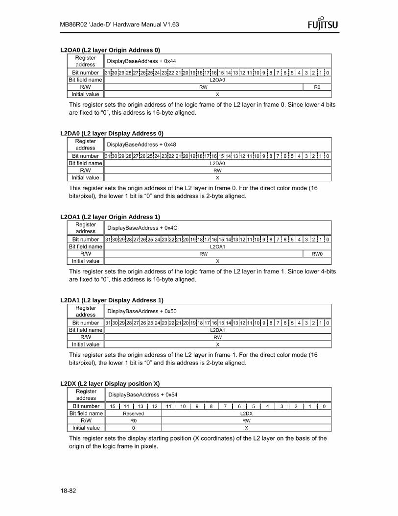
18-82
MB86R02 ‘Jade-D’ Hardware Manual V1.63
L2OA0 (L2 layer Origin Address 0) Register address
DisplayBaseAddress + 0x44
Bit number 31 30 29 28 27 26 25 24 23 22 21 20 19 18 17 16 15 14 13 12 11 10 9 8 7 6 5 4 3 2 1 0
Bit field name L2OA0
R/W RW R0
Initial value X
This register sets the origin address of the logic frame of the L2 layer in frame 0. Since lower 4 bits are fixed to “0”, this address is 16-byte aligned.
L2DA0 (L2 layer Display Address 0) Register address
DisplayBaseAddress + 0x48
Bit number 31 30 29 28 27 26 25 24 23 22 21 20 19 18 17 16 15 14 13 12 11 10 9 8 7 6 5 4 3 2 1 0
Bit field name L2DA0
R/W RW
Initial value X
This register sets the origin address of the L2 layer in frame 0. For the direct color mode (16 bits/pixel), the lower 1 bit is “0” and this address is 2-byte aligned.
L2OA1 (L2 layer Origin Address 1) Register address
DisplayBaseAddress + 0x4C
Bit number 31 30 29 28 27 26 25 24 23 22 21 20 19 18 17 16 15 14 13 12 11 10 9 8 7 6 5 4 3 2 1 0
Bit field name L2OA1
R/W RW RW0
Initial value X
This register sets the origin address of the logic frame of the L2 layer in frame 1. Since lower 4-bits are fixed to “0”, this address is 16-byte aligned.
L2DA1 (L2 layer Display Address 1) Register address
DisplayBaseAddress + 0x50
Bit number 31 30 29 28 27 26 25 24 23 22 21 20 19 18 17 16 15 14 13 12 11 10 9 8 7 6 5 4 3 2 1 0
Bit field name L2DA1
R/W RW
Initial value X
This register sets the origin address of the L2 layer in frame 1. For the direct color mode (16 bits/pixel), the lower 1 bit is “0” and this address is 2-byte aligned.
L2DX (L2 layer Display position X) Register address
DisplayBaseAddress + 0x54
Bit number 15 14 13 12 11 10 9 8 7 6 5 4 3 2 1 0
Bit field name Reserved L2DX
R/W R0 RW
Initial value 0 X
This register sets the display starting position (X coordinates) of the L2 layer on the basis of the origin of the logic frame in pixels.

18-83
MB86R02 ‘Jade-D’ Hardware Manual V1.63
L2DY (L2 layer Display position Y) Register address
DisplayBaseAddress + 0x56
Bit number 15 14 13 12 11 10 9 8 7 6 5 4 3 2 1 0
Bit field name Reserved L2DY
R/W R0 RW
Initial value 0 X
This register sets the display starting position (Y coordinates) of the L2 layer on the basis of the origin of the logic frame in pixels.
L2WX (L2 layer Window position X) Register address
DisplayBaseAddress + 0x134
Bit number 15 14 13 12 11 10 9 8 7 6 5 4 3 2 1 0
Bit field name Reserved L2WX
R/W R0 RW
Initial value 0 X
This register sets the X coordinates of the display position of the L2 layer window.
L2WY (L2 layer Window position Y) Register address
DisplayBaseAddress + 0x136
Bit number 15 14 13 12 11 10 9 8 7 6 5 4 3 2 1 0
Bit field name Reserved L2WY
R/W R0 RW
Initial value 0 Don’t care
This register sets the Y coordinates of the display position of the L2 layer window.
L2WW (L2 layer Window Width) Register address
DisplayBaseAddress + 0x138
Bit number 15 14 13 12 11 10 9 8 7 6 5 4 3 2 1 0
Bit field name Reserved L2WW
R/W R0 RW
Initial value 0 X
This register controls the horizontal direction display size (width) of the L2 layer window. Do not specify “0”.
L2WH (L2 layer Window Height) Register address
DisplayBaseAddress + 0x13A
Bit number 15 14 13 12 11 10 9 8 7 6 5 4 3 2 1 0
Bit field name Reserved L2WH
R/W R0 RW
Initial value 0 X
This register controls the vertical direction display size (height) of the L2 layer window. Setting value + 1 is the height.

18-84
MB86R02 ‘Jade-D’ Hardware Manual V1.63
L3M (L3 layer Mode) Register address
DisplayBaseAddress + 0x58
Bit number 31 30 29 28 27 26 25 24 23 22 21 --- 17 16 15 14 13 12 11 10 9 8 ---- 2 1 0
Bit field name L3C L3FLP Reserved L3W Reserved L3H
R/W RW RW R0 RW R0 RW
Initial value 0 0 0 X 0 X
Bit 11 to 0 L3H (L3 layer Height)
Specifies the height of the logic frame of the L3 layer in pixel units. Setting value + 1 is the height
Bit 23 to 16 L3W (L3 layer memory Width)
Sets the memory width (stride) of the logic frame of the L3 layer in 64-byte units
Bit 30 and 29 L3FLP (L3 layer Flip mode)
Sets flipping mode for L3 layer
00 Displays frame 0
01 Displays frame 1
10 Switches frame 0 and 1 alternately for display
11 Reserved
Bit 31 L3C (L3 layer Color mode)
Sets the color mode for L3 layer
0 Indirect color (8 bits/pixel) mode ARGB
1 Direct color (16 bits/pixel) mode ARGB

18-85
MB86R02 ‘Jade-D’ Hardware Manual V1.63
L3EM (L3 layer Extended Mode) Register address
DisplayBaseAddress + 0x140
Bit number 31 30 29 28 27 26 25 24 23 22 21 20 19 18 17 16 15 14 13 12 11 10 4 3 2 1 0
Bit field name L3EC Reserved L3PB Reserved L3OM L3WP
R/W RW R0 RW R0 RW RW
Initial value 00 0 0 0 0
Bit 0 L3 WP (L3 layer Window Position enable)
Selects the display position of L3 layer
0 Compatibility mode display (MR layer supported)
1 Window display
Bit 1 L3OM (L3 layer Overlay Mode)
Selects the overlay mode for L3 layer
0 Compatibility mode
1 Extended mode
Bit 23 to 20 L3PB (L3 layer Palette Base)
Shows the value added to the index when subtracting palette of L3 layer. 16 times of setting value is added.
Bit 31 and 30 L3EC (L3 layer Extended Color mode)
Sets extended color mode for L3 layer
00 Mode determined by L3C
01 Direct color (24 bits/pixel) mode
10 16bpp RGBA
11 24 bpp RGBA
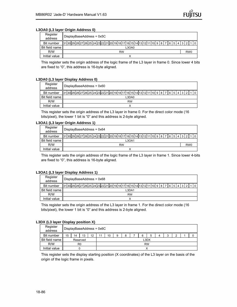
18-86
MB86R02 ‘Jade-D’ Hardware Manual V1.63
L3OA0 (L3 layer Origin Address 0) Register address
DisplayBaseAddress + 0x5C
Bit number 31 30 29 28 27 26 25 24 23 22 21 20 19 18 17 16 15 14 13 12 11 10 9 8 7 6 5 4 3 2 1 0
Bit field name L3OA0
R/W RW RW0
Initial value X
This register sets the origin address of the logic frame of the L3 layer in frame 0. Since lower 4 bits are fixed to “0”, this address is 16-byte aligned.
L3DA0 (L3 layer Display Address 0) Register address
DisplayBaseAddress + 0x60
Bit number 31 30 29 28 27 26 25 24 23 22 21 20 19 18 17 16 15 14 13 12 11 10 9 8 7 6 5 4 3 2 1 0
Bit field name L3DA0
R/W RW
Initial value X
This register sets the origin address of the L3 layer in frame 0. For the direct color mode (16 bits/pixel), the lower 1 bit is “0” and this address is 2-byte aligned.
L3OA1 (L3 layer Origin Address 1) Register address
DisplayBaseAddress + 0x64
Bit number 31 30 29 28 27 26 25 24 23 22 21 20 19 18 17 16 15 14 13 12 11 10 9 8 7 6 5 4 3 2 1 0
Bit field name L3OA1
R/W RW RW0
Initial value X
This register sets the origin address of the logic frame of the L3 layer in frame 1. Since lower 4-bits are fixed to “0”, this address is 16-byte aligned.
L3OA1 (L3 layer Display Address 1) Register address
DisplayBaseAddress + 0x68
Bit number 31 30 29 28 27 26 25 24 23 22 21 20 19 18 17 16 15 14 13 12 11 10 9 8 7 6 5 4 3 2 1 0
Bit field name L3DA1
R/W RW
Initial value X
This register sets the origin address of the L3 layer in frame 1. For the direct color mode (16 bits/pixel), the lower 1 bit is “0” and this address is 2-byte aligned.
L3DX (L3 layer Display position X) Register address
DisplayBaseAddress + 0x6C
Bit number 15 14 13 12 11 10 9 8 7 6 5 4 3 2 1 0
Bit field name Reserved L3DX
R/W R0 RW
Initial value 0 X
This register sets the display starting position (X coordinates) of the L3 layer on the basis of the origin of the logic frame in pixels.

18-87
MB86R02 ‘Jade-D’ Hardware Manual V1.63
L3DY (L3 layer Display position Y) Register address
DisplayBaseAddress + 0x6E
Bit number 15 14 13 12 11 10 9 8 7 6 5 4 3 2 1 0
Bit field name Reserved L3DY
R/W R0 RW
Initial value 0 X
This register sets the display starting position (Y coordinates) of the L3 layer on the basis of the origin of the logic frame in pixels.
L3WX (L3 layer Window position X) Register address
DisplayBaseAddress + 0x144
Bit number 15 14 13 12 11 10 9 8 7 6 5 4 3 2 1 0
Bit field name Reserved L3WX
R/W R0 RW
Initial value 0 X
This register sets the X coordinates of the display position of the L3 layer window.
L3WY (L3 layer Window position Y) Register address
DisplayBaseAddress + 0x146
Bit number 15 14 13 12 11 10 9 8 7 6 5 4 3 2 1 0
Bit field name Reserved L3WY
R/W R0 RW
Initial value 0 X
This register sets the Y coordinates of the display position of the L3 layer window.
L3WW (L3 layer Window Width) Register address
DisplayBaseAddress + 0x148
Bit number 15 14 13 12 11 10 9 8 7 6 5 4 3 2 1 0
Bit field name Reserved L3WW
R/W R0 RW
Initial value 0 X
This register controls the horizontal direction display size (width) of the L3 layer window. Do not specify “0”.
L3WH (L3-layer Window Height) Register address
DisplayBaseAddress + 0x14A
Bit number 15 14 13 12 11 10 9 8 7 6 5 4 3 2 1 0
Bit field name Reserved L3WH
R/W R0 RW
Initial value 0 X
This register controls the vertical direction display size (height) of the L3 layer window. Setting value + 1 is the height.

18-88
MB86R02 ‘Jade-D’ Hardware Manual V1.63
L4M (L4 layer Mode) Register address
DisplayBaseAddress + 0x70
Bit number 31 30 29 28 27 26 25 24 23 22 21 --- 17 16 15 14 13 12 11 10 9 8 ---- 2 1 0
Bit field name L4C L4FLP Reserved L4W Reserved L4H
R/W RW RW R0 RW R0 RW
Initial value 0 0 0 X 0 X
Bit 11 to 0 L4H (L4 layer Height)
Specifies the height of the logic frame of the L4 layer in pixel units. Setting value + 1 is the height
Bit 23 to 16 L4W (L4 layer memory Width)
Sets the memory width (stride) logic frame of the L4 layer in 64-byte units
Bit 30 and 29 L4FLP (L4 layer Flip mode)
Sets flipping mode for L4 layer
00 Displays frame 0
01 Displays frame 1
10 Switches frame 0 and 1 alternately for display
11 Reserved
Bit 31 L4C (L4 layer Color mode)
Sets the color mode for L4 layer
0 Indirect color (8 bits/pixel) mode ARGB
1 Direct color (16 bits/pixel) mode ARGB
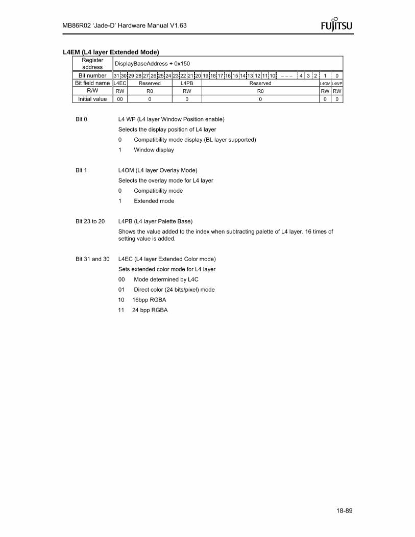
18-89
MB86R02 ‘Jade-D’ Hardware Manual V1.63
L4EM (L4 layer Extended Mode) Register address
DisplayBaseAddress + 0x150
Bit number 31 30 29 28 27 26 25 24 23 22 21 20 19 18 17 16 15 14 13 12 11 10 4 3 2 1 0
Bit field name L4EC Reserved L4PB Reserved L4OM L4WP
R/W RW R0 RW R0 RW RW
Initial value 00 0 0 0 0 0
Bit 0 L4 WP (L4 layer Window Position enable)
Selects the display position of L4 layer
0 Compatibility mode display (BL layer supported)
1 Window display
Bit 1 L4OM (L4 layer Overlay Mode)
Selects the overlay mode for L4 layer
0 Compatibility mode
1 Extended mode
Bit 23 to 20 L4PB (L4 layer Palette Base)
Shows the value added to the index when subtracting palette of L4 layer. 16 times of setting value is added.
Bit 31 and 30 L4EC (L4 layer Extended Color mode)
Sets extended color mode for L4 layer
00 Mode determined by L4C
01 Direct color (24 bits/pixel) mode
10 16bpp RGBA
11 24 bpp RGBA

18-90
MB86R02 ‘Jade-D’ Hardware Manual V1.63
L4OA0 (L4 layer Origin Address 0) Register address
DisplayBaseAddress + 0x74
Bit number 31 30 29 28 27 26 25 24 23 22 21 20 19 18 17 16 15 14 13 12 11 10 9 8 7 6 5 4 3 2 1 0
Bit field name L4OA0
R/W RW RW0
Initial value Don’t care
This register sets the origin address of the logic frame of the L4 layer in frame 0. Since lower 4 bits are fixed to “0”, this address is 16-byte aligned.
L4DA0 (L4 layer Display Address 0) Register address
DisplayBaseAddress + 0x78
Bit number 31 30 29 28 27 26 25 24 23 22 21 20 19 18 17 16 15 14 13 12 11 10 9 8 7 6 5 4 3 2 1 0
Bit field name L4DA0
R/W RW
Initial value X
This register sets the origin address of the L4 layer in frame 0. For the direct color mode (16 bits/pixel), the lower 1 bit is “0” and this address is 2-byte aligned.
L4OA1 (L4 layer Origin Address 1) Register address
DisplayBaseAddress + 0x7C
Bit number 31 30 29 28 27 26 25 24 23 22 21 20 19 18 17 16 15 14 13 12 11 10 9 8 7 6 5 4 3 2 1 0
Bit field name L4OA1
R/W RW RW0
Initial value X
This register sets the origin address of the logic frame of the L4 layer in frame 1. Since lower 4-bits are fixed to “0”, this address is 16-byte aligned.
L4OA1 (L4 layer Display Address 1) Register address
DisplayBaseAddress + 0x80
Bit number 31 30 29 28 27 26 25 24 23 22 21 20 19 18 17 16 15 14 13 12 11 10 9 8 7 6 5 4 3 2 1 0
Bit field name L4DA1
R/W RW
Initial value X
This register sets the origin address of the L4 layer in frame 1. For the direct color mode (16 bits/pixel), the lower 1 bit is “0” and this address is 2-byte aligned.
L4DX (L4 layer Display position X) Register address
DisplayBaseAddress + 0x84
Bit number 15 14 13 12 11 10 9 8 7 6 5 4 3 2 1 0
Bit field name Reserved L4DX
R/W R0 RW
Initial value 0 X
This register sets the display starting position (X coordinates) of the L4 layer on the basis of the origin of the logic frame in pixels.
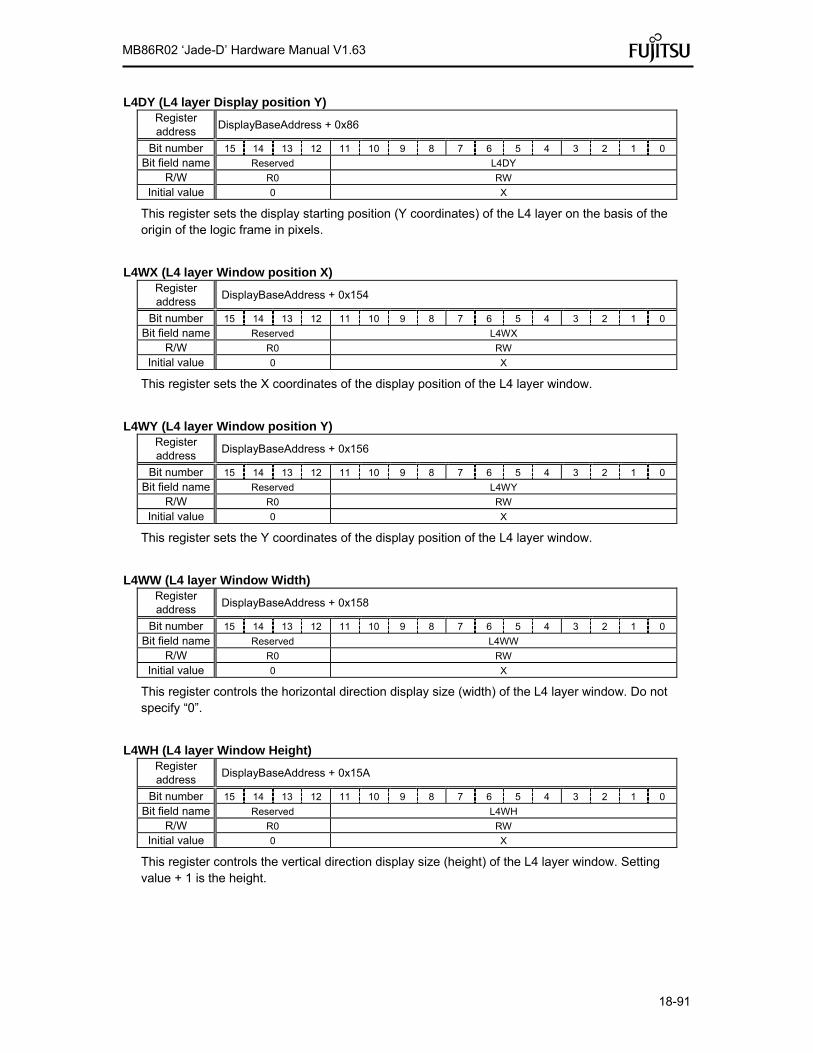
18-91
MB86R02 ‘Jade-D’ Hardware Manual V1.63
L4DY (L4 layer Display position Y) Register address
DisplayBaseAddress + 0x86
Bit number 15 14 13 12 11 10 9 8 7 6 5 4 3 2 1 0
Bit field name Reserved L4DY
R/W R0 RW
Initial value 0 X
This register sets the display starting position (Y coordinates) of the L4 layer on the basis of the origin of the logic frame in pixels.
L4WX (L4 layer Window position X) Register address
DisplayBaseAddress + 0x154
Bit number 15 14 13 12 11 10 9 8 7 6 5 4 3 2 1 0
Bit field name Reserved L4WX
R/W R0 RW
Initial value 0 X
This register sets the X coordinates of the display position of the L4 layer window.
L4WY (L4 layer Window position Y) Register address
DisplayBaseAddress + 0x156
Bit number 15 14 13 12 11 10 9 8 7 6 5 4 3 2 1 0
Bit field name Reserved L4WY
R/W R0 RW
Initial value 0 X
This register sets the Y coordinates of the display position of the L4 layer window.
L4WW (L4 layer Window Width) Register address
DisplayBaseAddress + 0x158
Bit number 15 14 13 12 11 10 9 8 7 6 5 4 3 2 1 0
Bit field name Reserved L4WW
R/W R0 RW
Initial value 0 X
This register controls the horizontal direction display size (width) of the L4 layer window. Do not specify “0”.
L4WH (L4 layer Window Height) Register address
DisplayBaseAddress + 0x15A
Bit number 15 14 13 12 11 10 9 8 7 6 5 4 3 2 1 0
Bit field name Reserved L4WH
R/W R0 RW
Initial value 0 X
This register controls the vertical direction display size (height) of the L4 layer window. Setting value + 1 is the height.
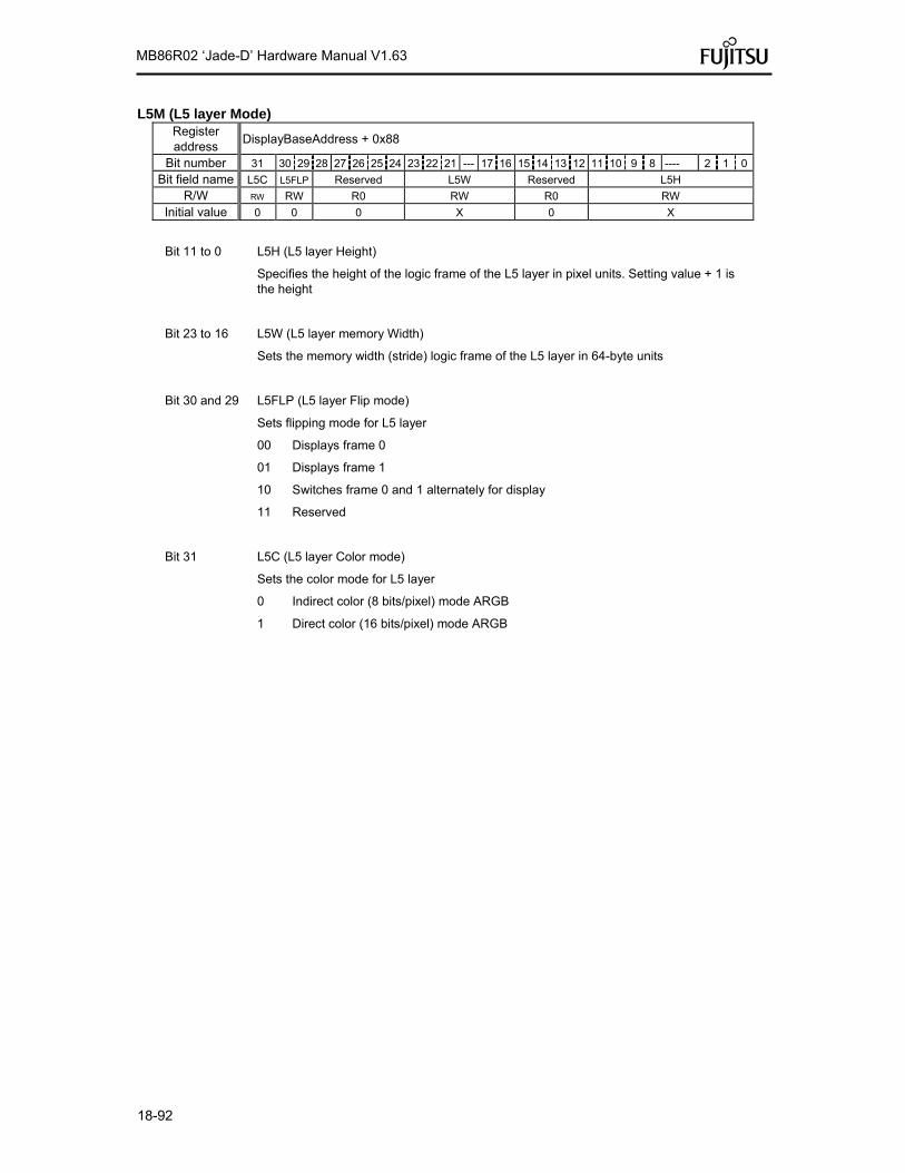
18-92
MB86R02 ‘Jade-D’ Hardware Manual V1.63
L5M (L5 layer Mode) Register address
DisplayBaseAddress + 0x88
Bit number 31 30 29 28 27 26 25 24 23 22 21 --- 17 16 15 14 13 12 11 10 9 8 ---- 2 1 0
Bit field name L5C L5FLP Reserved L5W Reserved L5H
R/W RW RW R0 RW R0 RW
Initial value 0 0 0 X 0 X
Bit 11 to 0 L5H (L5 layer Height)
Specifies the height of the logic frame of the L5 layer in pixel units. Setting value + 1 is the height
Bit 23 to 16 L5W (L5 layer memory Width)
Sets the memory width (stride) logic frame of the L5 layer in 64-byte units
Bit 30 and 29 L5FLP (L5 layer Flip mode)
Sets flipping mode for L5 layer
00 Displays frame 0
01 Displays frame 1
10 Switches frame 0 and 1 alternately for display
11 Reserved
Bit 31 L5C (L5 layer Color mode)
Sets the color mode for L5 layer
0 Indirect color (8 bits/pixel) mode ARGB
1 Direct color (16 bits/pixel) mode ARGB
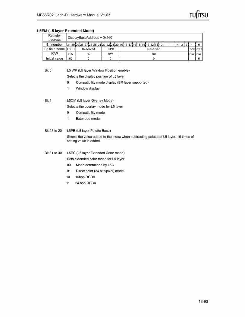
18-93
MB86R02 ‘Jade-D’ Hardware Manual V1.63
L5EM (L5 layer Extended Mode) Register address
DisplayBaseAddress + 0x160
Bit number 31 30 29 28 27 26 25 24 23 22 21 20 19 18 17 16 15 14 13 12 11 10 4 3 2 1 0
Bit field name L5EC Reserved L5PB Reserved L5OM L5WP
R/W RW R0 RW R0 RW RW
Initial value 00 0 0 0 0
Bit 0 L5 WP (L5 layer Window Position enable)
Selects the display position of L5 layer
0 Compatibility mode display (BR layer supported)
1 Window display
Bit 1 L5OM (L5 layer Overlay Mode)
Selects the overlay mode for L5 layer
0 Compatibility mode
1 Extended mode
Bit 23 to 20 L5PB (L5 layer Palette Base)
Shows the value added to the index when subtracting palette of L5 layer. 16 times of setting value is added.
Bit 31 to 30 L5EC (L5 layer Extended Color mode)
Sets extended color mode for L5 layer
00 Mode determined by L5C
01 Direct color (24 bits/pixel) mode
10 16bpp RGBA
11 24 bpp RGBA

18-94
MB86R02 ‘Jade-D’ Hardware Manual V1.63
L5OA0 (L5 layer Origin Address 0) Register address
DisplayBaseAddress + 0x8C
Bit number 31 30 29 28 27 26 25 24 23 22 21 20 19 18 17 16 15 14 13 12 11 10 9 8 7 6 5 4 3 2 1 0
Bit field name BROA0
R/W RW RW0
Initial value X
This register sets the origin address of the logic frame of the L5 layer in frame 0. Since lower 4 bits are fixed to “0”, this address is 16-byte aligned.
L5DA0 (L5 layer Display Address 0) Register address
DisplayBaseAddress + 0x90
Bit number 31 30 29 28 27 26 25 24 23 22 21 20 19 18 17 16 15 14 13 12 11 10 9 8 7 6 5 4 3 2 1 0
Bit field name L5DA0
R/W RW
Initial value X
This register sets the origin address of the L5 layer in frame 0. For the direct color mode (16 bits/pixel), the lower 1 bit is “0” and this address is 2-byte aligned.
L5OA1 (L5 layer Origin Address 1) Register address
DisplayBaseAddress + 0x94
Bit number 31 30 29 28 27 26 25 24 23 22 21 20 19 18 17 16 15 14 13 12 11 10 9 8 7 6 5 4 3 2 1 0
Bit field name L5OA1
R/W RW RW0
Initial value X
This register sets the origin address of the logic frame of the L5 layer in frame 1. Since lower 4-bits are fixed to “0”, this address is 16-byte aligned.
L5OA1 (L5 layer Display Address 1) Register address
DisplayBaseAddress + 0x98
Bit number 31 30 29 28 27 26 25 24 23 22 21 20 19 18 17 16 15 14 13 12 11 10 9 8 7 6 5 4 3 2 1 0
Bit field name L5DA1
R/W RW
Initial value X
This register sets the origin address of the L5 layer in frame 1. For the direct color mode (16 bits/pixel), the lower 1 bit is “0” and this address is 2-byte aligned.
L5DX (L5 layer Display position X) Register address
DisplayBaseAddress + 0x9C
Bit number 15 14 13 12 11 10 9 8 7 6 5 4 3 2 1 0
Bit field name Reserved L5DX
R/W R0 RW
Initial value 0 X
This register sets the display starting position (X coordinates) of the L5 layer on the basis of the origin of the logic frame in pixels.

18-95
MB86R02 ‘Jade-D’ Hardware Manual V1.63
L5DY (L5 layer Display position Y) Register address
DisplayBaseAddress + 0x9E
Bit number 15 14 13 12 11 10 9 8 7 6 5 4 3 2 1 0
Bit field name Reserved L5DY
R/W R0 RW
Initial value 0 X
This register sets the display starting position (Y coordinates) of the L5 layer on the basis of the origin of the logic frame in pixels.
L5WX (L5 layer Window position X) Register address
DisplayBaseAddress + 0x164
Bit number 15 14 13 12 11 10 9 8 7 6 5 4 3 2 1 0
Bit field name Reserved L5WX
R/W R0 RW
Initial value 0 X
This register sets the X coordinates of the display position of the L5 layer window.
L5WY (L5 layer Window position Y) Register address
DisplayBaseAddress + 0x166
Bit number 15 14 13 12 11 10 9 8 7 6 5 4 3 2 1 0
Bit field name Reserved L5WY
R/W R0 RW
Initial value 0 X
This register sets the Y coordinates of the display position of the L5 layer window.
L5WW (L5 layer Window Width) Register address
DisplayBaseAddress + 0x168
Bit number 15 14 13 12 11 10 9 8 7 6 5 4 3 2 1 0
Bit field name Reserved L5WW
R/W R0 RW
Initial value 0 X
This register controls the horizontal direction display size (width) of the L5 layer window. Do not specify “0”.
L5WH (L5 layer Window Height) Register address
DisplayBaseAddress + 0x16A
Bit number 15 14 13 12 11 10 9 8 7 6 5 4 3 2 1 0
Bit field name Reserved L5WH
R/W R0 RW
Initial value 0 X
This register controls the vertical direction display size (height) of the L5 layer window. Setting value + 1 is the height.

18-96
MB86R02 ‘Jade-D’ Hardware Manual V1.63
CUTC (Cursor Transparent Control) Register address
DisplayBaseAddress + 0xA0
Bit number 15 14 13 12 11 10 9 8 7 6 5 4 3 2 1 0
Bit field name Reserved CUZT CUTC
R/W R0 RW RW
Initial value 0 X X
Bit 7 to 0 CUTC (Cursor Transparent Code)
Sets color code handled as transparent code
Bit 8 CUZT (Cursor Zero Transparency)
Defines handling of color code 0
0 Code 0 as non-transparency color
1 Code 0 as transparency color
CPM (Cursor Priority Mode) Register address
DisplayBaseAddress + 0xA2
Bit number 7 6 5 4 3 2 1 0
Bit field name Reserved CEN1 CEN0 Reserved CUO1 CUO0
R/W R0 RW RW R0 RW RW
Initial value 0 0 0 0 0 0
This register controls the display priority of cursors. Cursor 0 is always preferred to cursor 1.
Bit 0 CUO0 (Cursor Overlap 0)
Sets display priority between cursor 0 and pixels of Console layer
0 Puts cursor 0 at lower than L0 layer.
1 Puts cursor 0 at higher than L0 layer.
Bit 1 CUO1 (Cursor Overlap 1)
Sets display priority between cursor 1 and C layer
0 Puts cursor 1 at lower than L0 layer.
1 Puts cursor 1 at lower than L0 layer.
Bit 4 CEN0 (Cursor Enable 0)
Sets enabling display of cursor 0
0 Disabled
1 Enabled
Bit 5 CEN1 (Cursor Enable 1)
Sets enabling display of cursor 1
0 Disabled
1 Enabled
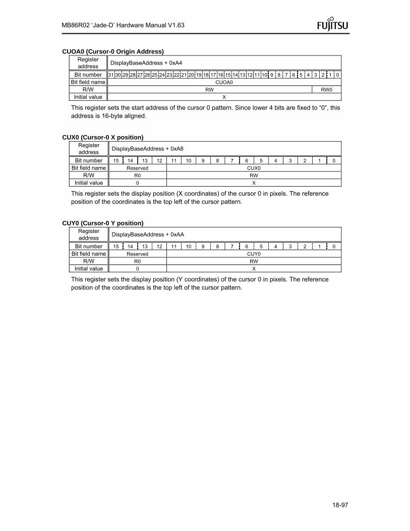
18-97
MB86R02 ‘Jade-D’ Hardware Manual V1.63
CUOA0 (Cursor-0 Origin Address) Register address
DisplayBaseAddress + 0xA4
Bit number 31 30 29 28 27 26 25 24 23 22 21 20 19 18 17 16 15 14 13 12 11 10 9 8 7 6 5 4 3 2 1 0
Bit field name CUOA0
R/W RW RW0
Initial value X
This register sets the start address of the cursor 0 pattern. Since lower 4 bits are fixed to “0”, this address is 16-byte aligned.
CUX0 (Cursor-0 X position) Register address
DisplayBaseAddress + 0xA8
Bit number 15 14 13 12 11 10 9 8 7 6 5 4 3 2 1 0
Bit field name Reserved CUX0
R/W R0 RW
Initial value 0 X
This register sets the display position (X coordinates) of the cursor 0 in pixels. The reference position of the coordinates is the top left of the cursor pattern.
CUY0 (Cursor-0 Y position) Register address
DisplayBaseAddress + 0xAA
Bit number 15 14 13 12 11 10 9 8 7 6 5 4 3 2 1 0
Bit field name Reserved CUY0
R/W R0 RW
Initial value 0 X
This register sets the display position (Y coordinates) of the cursor 0 in pixels. The reference position of the coordinates is the top left of the cursor pattern.

18-98
MB86R02 ‘Jade-D’ Hardware Manual V1.63
CUOA1 (Cursor-1 Origin Address) Register address
DisplayBaseAddress + 0xAC
Bit number 31 30 29 28 27 26 25 24 23 22 21 20 19 18 17 16 15 14 13 12 11 10 9 8 7 6 5 4 3 2 1 0
Bit field name CUOA1
R/W RW RW0
Initial value X
This register sets the start address of the cursor 1 pattern. Since lower 4 bits are fixed to “0”, this address is 16-byte aligned.
CUX1 (Cursor-1 X position) Register address
DisplayBaseAddress + 0xB0
Bit number 15 14 13 12 11 10 9 8 7 6 5 4 3 2 1 0
Bit field name Reserved CUX1
R/W R0 RW
Initial value 0 X
This register sets the display position (X coordinates) of the cursor 1 in pixels. The reference position of the coordinates is the top left of the cursor pattern.
CUY1 (Cursor-1 Y position) Register address
DisplayBaseAddress + 0xB2
Bit number 15 14 13 12 11 10 9 8 7 6 5 4 3 2 1 0
Bit field name Reserved CUY1
R/W R0 RW
Initial value 0 X
This register sets the display position (Y coordinates) of the cursor 1 in pixels. The reference position of the coordinates is the top left of the cursor pattern.

18-99
MB86R02 ‘Jade-D’ Hardware Manual V1.63
MDC (Multi Display Control)
Register address
DisplayBaseAddress + 0x170
Bit number 31 30 29 28 24 23 22 21 20 19 18 17 16 15 14 13 12 11 10 9 7 6 5 4 3 2 1 0
Bit field name MDen reserve SC1en SC0en
R/W RW R0 RW RW
Initial value 0 0 X X
This register controls dual display mode.
Bit 0 SC0en0 (screen 0 enable 0)
0: L0 is not included into screen 0
1: L0 is included into screen 0
Bit 1 SC0en1 (screen 0 enable 1)
0: L1 is not included into screen 0
1: L1 is included into screen 0
Bit 5 SC0en5 (screen 0 enable 5)
0: L5 is not included into screen 0
1: L5 is included into screen 0
Bit 6 SC0en6 (screen 0 enable 6)
0: Cursor0 is not included into screen 0
1: Cursor0 is included into screen 0
Bit 7 SC0en7 (screen 0 enable 7)
0: Cursor1 is not included into screen 0
1: Cursor1 is included into screen 0
Bit 8 SC1en0 (screen 1 enable 0)
0: L0 is not included into screen 1
1: L0 is included into screen 1
Bit 9 SC1en1 (screen 1 enable 1)
0: L1 is not included into screen 1
1: L1 is included into screen 1
Bit 13 SC1en5 (screen 1 enable 5)
0: L5 is not included into screen 1
1: L5 is included into screen 1

18-100
MB86R02 ‘Jade-D’ Hardware Manual V1.63
Bit 14 SC1en6 (screen 1 enable 6)
0: Cursor 0 is not included into screen 1
1: Cursor 0 is included into screen 1
Bit 15 SC1en7 (screen 1 enable 7)
0: Cursor 1 is not included into screen 1
1: Cursor 1 is included into screen 1
Bit 31 MDen (multi display enable)
This enables multi or dual display mode
0: Single display mode
1: Dual display mode

18-101
MB86R02 ‘Jade-D’ Hardware Manual V1.63
DLS (Display Layer Select) Register address
DisplayBaseAddress + 0x180
Bit number 31 30 29 ----- 25 24 23 22 21 20 19 18 17 16 15 14 13 12 11 10 9 8 7 6 5 4 3 2 1 0
Bit field name Reserved DLS5 DLS4 DLS3 DLS2 DLS1 DSL0
R/W RW0 R0 RW R0 RW R0 RW R0 RW R0 RW R0 RW
Initial value 0 0 101 0 100 0 011 0 010 0 001 0 000
This register defines the blending sequence.
Bit 3 to 0 DSL0 (Display Layer Select 0)
Selects the top layer subjected to blending.
0000 L0 layer
0001 L1 layer
: :
0101 L5 layer
0110 Reserved
: :
0110 Reserved
0111 Not selected
Bit 7 to 4 DSL1 (Display Layer Select 1)
Selects the second layer subjected to blending. The bit values are the same as DSL0.
Bit 11 to 8 DSL2 (Display Layer Select 2)
Selects the third layer subjected to blending. The bit values are the same as DSL0.
Bit 15 to 12 DSL3 (Display Layer Select 3)
Selects the fourth layer subjected to blending. The bit values are the same as DSL0.
Bit 19 to 16 DSL4 (Display Layer Select 4)
Selects the fifth layer subjected to blending. The bit values are the same as DSL0.
Bit 23 to 20 DSL5 (Display Layer Select 5)
Selects the bottom layer subjected to blending. The bit values are the same as DSL0.

18-102
MB86R02 ‘Jade-D’ Hardware Manual V1.63
DBGC (Display Background Color) Register address
DisplayBaseAddress + 0x184
Bit number 31 30 29 ----- 25 24 23 22 21 20 19 18 17 16 15 14 13 12 11 10 9 8 7 6 5 4 3 2 1 0
Bit field name Reserved DBGR DBGG DBGB
R/W R0
Initial value
This register specifies the color to be displayed in areas outside the display area of each layer on the window.
Bit 7 to 0 DBGB (Display Background Blue)
Specifies the blue level of the background color.
Bit 15 to 8 DBGG (Display Background Green)
Specifies the green level of the background color.
Bit 23 to 16 DBGR (Display Background Red)
Specifies the red level of the background color.

18-103
MB86R02 ‘Jade-D’ Hardware Manual V1.63
L0BLD (L0 Blend) Register address
DisplayBaseAddress + 0xB4
Bit number 31 30 29 28 ----- 20 19 18 17 16 15 14 13 12 11 10 9 8 7 6 5 4 3 2 1 0
Bit field name Reserved L0BE L0BS L0BI L0BP Reserved L0BR
R/W R0 RW RW RW RW RW0 RW
Initial value 0 0 X X X 0 X
This register specifies the blend parameters for the L0 layer. This register corresponds to BRATIO or BMODE for previous products.
Bit 7 to 0 L0BR (L0 layer Blend Ratio)
Sets the blend ratio. Basically, the blend ratio is setting value/256.
Bit 13 L0BP (L0 layer Blend Plane)
Specifies that the L5 layer is the blend plane.
0 Value of L0BR used as blend ratio
1 Pixel of L5 layer used as blend ratio
Bit 14 L0BI (L0 layer Blend Increment)
Selects whether or not 1/256 is added when the blend ratio is not “0”.
0 Blend ratio calculated as is
1 1/256 added when blend ratio 0
Bit 15 L0BS (L0 layer Blend Select)
Selects the blend calculation expression.
0 Upper image Blend ratio Lower image (1 – Blend ratio)
1 Upper image (1 – Blend ratio) Lower image Blend ratio
Bit 16 L0BE (L0 layer Blend Enable)
This bit enables blending.
0 Overlay via transparent color
1 Overlay via blending
Before blending, the blend mode must be specified using L0BE and alpha must also be enabled for L0 layer display data. For direct color, alpha is specified using the MSB of data; for indirect color, alpha is specified using the MSB of palette data.

18-104
MB86R02 ‘Jade-D’ Hardware Manual V1.63
L1BLD (L1 Blend) Register address
DisplayBaseAddress + 0x188
Bit number 31 30 29 28 ----- 20 19 18 17 16 15 14 13 12 11 10 9 8 7 6 5 4 3 2 1 0
Bit field name Reserved L1BE L1BS L1BI L1BP Reserved L1BR
R/W R0 RW RW RW RW RW0 RW
Initial value 0 0 X X X 0 X
This register specifies the blend parameters for the L1 layer.
Bit 7 to 0 L1BR (L1 layer Blend Ratio)
Sets the blend ratio. Basically, the blend ratio is setting value/256.
Bit 13 L1BP (L1 layer Blend Plane)
Specifies that the L5 layer is the blend plane.
0 Value of L1BR used as blend ratio
1 Pixel of L5 layer used as blend ratio
Bit 14 L1BI (L1 layer Blend Increment)
Selects whether or not 1/256 is added when the blend ratio is not “0”.
0 Blend ratio calculated as is
1 1/256 added when blend ratio 0
Bit 15 L1BS (L1 layer Blend Select)
Selects the blend calculation expression.
0 Upper image Blend ratio Lower image (1 – Blend ratio)
1 Upper image (1 – Blend ratio) Lower image Blend ratio
Bit 16 L1BE (L1 layer Blend Enable)
This bit enables blending.
0 Overlay via transparent color
1 Overlay via blending
Before blending, the blend mode must be specified using L1BE and alpha must also be enabled for L1 layer display data. For direct color, alpha is specified using the MSB of data; for indirect color, alpha is specified using the MSB of palette data.
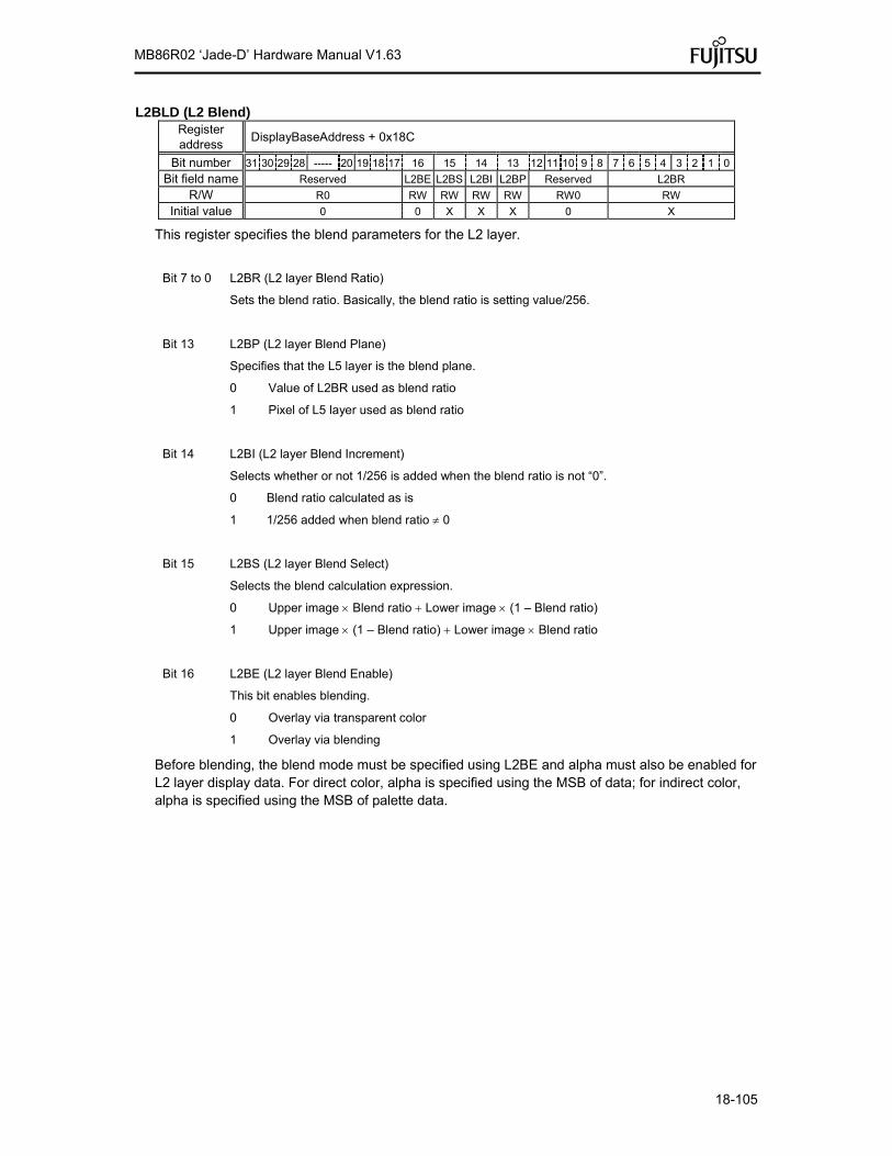
18-105
MB86R02 ‘Jade-D’ Hardware Manual V1.63
L2BLD (L2 Blend) Register address
DisplayBaseAddress + 0x18C
Bit number 31 30 29 28 ----- 20 19 18 17 16 15 14 13 12 11 10 9 8 7 6 5 4 3 2 1 0
Bit field name Reserved L2BE L2BS L2BI L2BP Reserved L2BR
R/W R0 RW RW RW RW RW0 RW
Initial value 0 0 X X X 0 X
This register specifies the blend parameters for the L2 layer.
Bit 7 to 0 L2BR (L2 layer Blend Ratio)
Sets the blend ratio. Basically, the blend ratio is setting value/256.
Bit 13 L2BP (L2 layer Blend Plane)
Specifies that the L5 layer is the blend plane.
0 Value of L2BR used as blend ratio
1 Pixel of L5 layer used as blend ratio
Bit 14 L2BI (L2 layer Blend Increment)
Selects whether or not 1/256 is added when the blend ratio is not “0”.
0 Blend ratio calculated as is
1 1/256 added when blend ratio 0
Bit 15 L2BS (L2 layer Blend Select)
Selects the blend calculation expression.
0 Upper image Blend ratio Lower image (1 – Blend ratio)
1 Upper image (1 – Blend ratio) Lower image Blend ratio
Bit 16 L2BE (L2 layer Blend Enable)
This bit enables blending.
0 Overlay via transparent color
1 Overlay via blending
Before blending, the blend mode must be specified using L2BE and alpha must also be enabled for L2 layer display data. For direct color, alpha is specified using the MSB of data; for indirect color, alpha is specified using the MSB of palette data.
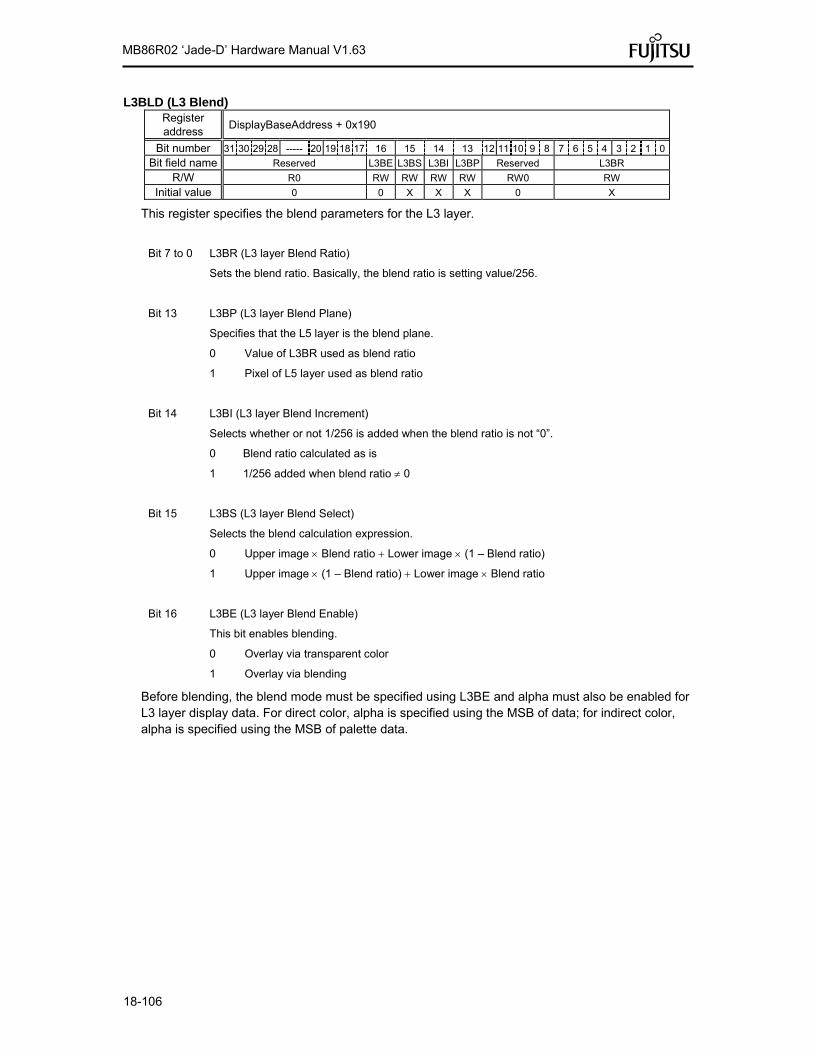
18-106
MB86R02 ‘Jade-D’ Hardware Manual V1.63
L3BLD (L3 Blend) Register address
DisplayBaseAddress + 0x190
Bit number 31 30 29 28 ----- 20 19 18 17 16 15 14 13 12 11 10 9 8 7 6 5 4 3 2 1 0
Bit field name Reserved L3BE L3BS L3BI L3BP Reserved L3BR
R/W R0 RW RW RW RW RW0 RW
Initial value 0 0 X X X 0 X
This register specifies the blend parameters for the L3 layer.
Bit 7 to 0 L3BR (L3 layer Blend Ratio)
Sets the blend ratio. Basically, the blend ratio is setting value/256.
Bit 13 L3BP (L3 layer Blend Plane)
Specifies that the L5 layer is the blend plane.
0 Value of L3BR used as blend ratio
1 Pixel of L5 layer used as blend ratio
Bit 14 L3BI (L3 layer Blend Increment)
Selects whether or not 1/256 is added when the blend ratio is not “0”.
0 Blend ratio calculated as is
1 1/256 added when blend ratio 0
Bit 15 L3BS (L3 layer Blend Select)
Selects the blend calculation expression.
0 Upper image Blend ratio Lower image (1 – Blend ratio)
1 Upper image (1 – Blend ratio) Lower image Blend ratio
Bit 16 L3BE (L3 layer Blend Enable)
This bit enables blending.
0 Overlay via transparent color
1 Overlay via blending
Before blending, the blend mode must be specified using L3BE and alpha must also be enabled for L3 layer display data. For direct color, alpha is specified using the MSB of data; for indirect color, alpha is specified using the MSB of palette data.

18-107
MB86R02 ‘Jade-D’ Hardware Manual V1.63
L4BLD (L4 Blend) Register address
DisplayBaseAddress + 0x194
Bit number 31 30 29 28 ----- 20 19 18 17 16 15 14 13 12 11 10 9 8 7 6 5 4 3 2 1 0
Bit field name Reserved L4BE L4BS L4BI L4BP Reserved L4BR
R/W R0 RW RW RW RW RW0 RW
Initial value 0 0 X X X 0 X
This register specifies the blend parameters for the L4 layer.
Bit 7 to 0 L4BR (L4 layer Blend Ratio)
Sets the blend ratio. Basically, the blend ratio is setting value/256.
Bit 13 L4BP (L4 layer Blend Plane)
Specifies that the L5 layer is the blend plane.
0 Value of L4BR used as blend ratio
1 Pixel of L5 layer used as blend ratio
Bit 14 L4BI (L4 layer Blend Increment)
Selects whether or not 1/256 is added when the blend ratio is not “0”.
0 Blend ratio calculated as is
1 1/256 added when blend ratio 0
Bit 15 L4BS (L4 layer Blend Select)
Selects the blend calculation expression.
0 Upper image Blend ratio Lower image (1 – Blend ratio)
1 Upper image (1 – Blend ratio) Lower image Blend ratio
Bit 16 L4BE (L4 layer Blend Enable)
This bit enables blending.
0 Overlay via transparent color
1 Overlay via blending
Before blending, the blend mode must be specified using L4BE and alpha must also be enabled for L4 layer display data. For direct color, alpha is specified using the MSB of data; for indirect color, alpha is specified using the MSB of palette data.

18-108
MB86R02 ‘Jade-D’ Hardware Manual V1.63
L5BLD (L5 Blend) Register address
DisplayBaseAddress + 0x198
Bit number 31 30 29 28 ----- 21 20 19 18 17 16 15 14 13 12 11 10 9 8 7 6 5 4 3 2 1 0
Bit field name Reserved L5BE L5BS L5BI Reserved L5BR
R/W R0 RW RW RW RW RW0
Initial value 0 X X X 0 X
This register specifies the blend parameters for the L5 layer.
Bit 7 to 0 L5BR (L5 layer Blend Ratio)
Sets the blend ratio. Basically, the blend ratio is setting value/256.
Bit 14 L5BI (L5 layer Blend Increment)
Selects whether or not 1/256 is added when the blend ratio is not “0”.
0 Blend ratio calculated as is
1 1/256 added when blend ratio 0
Bit 15 L5BS (L5 layer Blend Select)
Selects the blend calculation expression.
0 Upper image Blend ratio Lower image (1 – Blend ratio)
1 Upper image (1 – Blend ratio) Lower image Blend ratio
Bit 16 L5BE (L5 layer Blend Enable)
This bit enables blending.
0 Overlay via transparent color
1 Overlay via blending
Before blending, the blend mode must be specified using L5BE and alpha must also be enabled for L5 layer display data. For direct color, alpha is specified using the MSB of data; for indirect color, alpha is specified using the MSB of palette data.

18-109
MB86R02 ‘Jade-D’ Hardware Manual V1.63
L0TC (L0 layer Transparency Control) Register address
DisplayBaseAddress + 0xBC
Bit number 15 14 13 12 11 10 9 8 7 6 5 4 3 2 1 0
Bit field name L0ZT L0TC
R/W RW RW
Initial value 0 Don’t care
This register sets the transparent color for the L0 layer. Color set by this register is transparent in blend mode. When L0TC 0 and L0ZT 0, color 0 is displayed in black (transparent).
This register corresponds to the CTC register for previous products.
Bit 14 to 0 L0TC (L0 layer Transparent Color)
Sets transparent color code for the L0 layer. In indirect color mode (8 bits/pixel) bits 7 to 0 are used.
Bit 15 L0ZT (L0 layer Zero Transparency)
Sets handling of color code 0 in L0 layer
0: Code 0 as transparency color
1: Code 0 as non-transparency color
L2TC (L2 layer Transparency Control) Register address
DisplayBaseAddress + 0xC2
Bit number 15 14 13 12 11 10 9 8 7 6 5 4 3 2 1 0
Bit field name L2ZT L2TC
R/W RW RW
Initial value 0 Don’t care
This register sets the transparent color for the L2 layer.
When L2TC 0 and L2ZT 0, color 0 is displayed in black (transparent).
This register corresponds to the MLTC register for previous products.
Bit 14 to 0 L2TC (L2 layer Transparent Color)
Sets transparent color code for the L2 layer. In indirect color mode (8 bits/pixel) bits 7 to 0 are used.
Bit 15 L2ZT (L2 layer Zero Transparency)
Sets handling of color code 0 in L2 layer
0 Code 0 as transparency color
1 Code 0 as non-transparency color

18-110
MB86R02 ‘Jade-D’ Hardware Manual V1.63
L3TC (L3 layer Transparency Control) Register address
DisplayBaseAddress + 0xC0
Bit number 15 14 13 12 11 10 9 8 7 6 5 4 3 2 1 0
Bit field name L3ZT L3TC
R/W RW RW
Initial value 0 Don’t care
This register sets the transparent color for the L3 layer. When L3TC 0 and L3ZT 0, color 0 is displayed in black (transparent).
This register corresponds to the MLTC register for previous products.
Bit 14 to 0 L3TC (L3 layer Transparent Color)
Sets transparent color code for the L3 layer. In indirect color mode (8 bits/pixel) bits 7 to 0 are used.
Bit 15 L3ZT (L3 layer Zero Transparency)
Sets handling of color code 0 in L3 layer
0 Code 0 as transparency color
1 Code 0 as non-transparency color
L0ETC (L0 layer Extend Transparency Control) Register address
DisplayBaseAddress + 0x1A0
Bit number 31 30 29 28 --- 24 23 22 21 20 19 18 17 16 15 14 13 12 11 10 9 8 7 6 5 4 3 2 1 0
Bit field name L0ETZ Reserved L0TEC
R/W RW R0 RW
Initial value 0 0
This register sets the transparent color for the L0 layer. The 24 bits/pixel transparent color is set using this register. The lower 15 bits of this register are physically the same as L0TC. Also, L0ETZ is physically the same as L0TZ.
When L0ETC 0 and L0EZT 0, color 0 is displayed in black (transparent).
Bit 23 to 0 L0ETC (L0 layer Extend Transparent Color)
Sets transparent color code for the L0 layer. In indirect color mode (8 bits/pixel) bits 7 to 0 are used.
Bit 31 L0EZT (L0 layer Extend Zero Transparency)
Sets handling of color code 0 in L0 layer
0 Code 0 as transparency color
1 Code 0 as non-transparency color
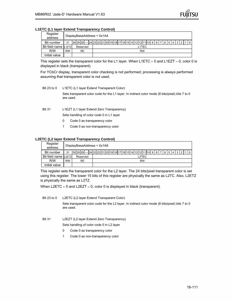
18-111
MB86R02 ‘Jade-D’ Hardware Manual V1.63
L1ETC (L1 layer Extend Transparency Control) Register address
DisplayBaseAddress + 0x1A4
Bit number 31 30 29 28 --- 24 23 22 21 20 19 18 17 16 15 14 13 12 11 10 9 8 7 6 5 4 3 2 1 0
Bit field name L1ETZ Reserved L1TEC
R/W RW R0 RW
Initial value
This register sets the transparent color for the L1 layer. When L1ETC 0 and L1EZT 0, color 0 is displayed in black (transparent).
For YCbCr display, transparent color checking is not performed; processing is always performed assuming that transparent color is not used.
Bit 23 to 0 L1ETC (L1 layer Extend Transparent Color)
Sets transparent color code for the L1 layer. In indirect color mode (8 bits/pixel) bits 7 to 0 are used.
Bit 31 L1EZT (L1 layer Extend Zero Transparency)
Sets handling of color code 0 in L1 layer
0 Code 0 as transparency color
1 Code 0 as non-transparency color
L2ETC (L2 layer Extend Transparency Control) Register address
DisplayBaseAddress + 0x1A8
Bit number 31 30 29 28 --- 24 23 22 21 20 19 18 17 16 15 14 13 12 11 10 9 8 7 6 5 4 3 2 1 0
Bit field name L2ETZ Reserved L2TEC
R/W RW R0 RW
Initial value
This register sets the transparent color for the L2 layer. The 24 bits/pixel transparent color is set using this register. The lower 15 bits of this register are physically the same as L2TC. Also, L2ETZ is physically the same as L2TZ.
When L2ETC 0 and L2EZT 0, color 0 is displayed in black (transparent).
Bit 23 to 0 L2ETC (L2 layer Extend Transparent Color)
Sets transparent color code for the L2 layer. In indirect color mode (8 bits/pixel) bits 7 to 0 are used.
Bit 31 L2EZT (L2 layer Extend Zero Transparency)
Sets handling of color code 0 in L2 layer
0 Code 0 as transparency color
1 Code 0 as non-transparency color

18-112
MB86R02 ‘Jade-D’ Hardware Manual V1.63
L3ETC (L3 layer Extend Transparency Control) Register address
DisplayBaseAddress + 0x1AC
Bit number 31 30 29 28 --- 24 23 22 21 20 19 18 17 16 15 14 13 12 11 10 9 8 7 6 5 4 3 2 1 0
Bit field name L3ETZ Reserved L3TEC
R/W RW R0 RW
Initial value 0 0
This register sets the transparent color for the L3 layer. The 24 bits/pixel transparent color is set using this register. The lower 15 bits of this register are physically the same as L3TC. Also, L3ETZ is physically the same as L3TZ.
When L3ETC 0 and L3EZT 0, color 0 is displayed in black (transparent).
Bit 23 to 0 L3ETC (L3 layer Extend Transparent Color)
Sets transparent color code for the L3 layer. In indirect color mode (8 bits/pixel) bits 7 to 0 are used.
Bit 31 L3EZT (L3 layer Extend Zero Transparency)
Sets handling of color code 0 in L3 layer
0 Code 0 as transparency color
1 Code 0 as non-transparency color
L4ETC (L4 layer Extend Transparency Control) Register address
DisplayBaseAddress + 0x1B0
Bit number 31 30 29 28 --- 24 23 22 21 20 19 18 17 16 15 14 13 12 11 10 9 8 7 6 5 4 3 2 1 0
Bit field name L4ETZ Reserved L4TEC
R/W RW R0 RW
Initial value 0 0
This register sets the transparent color for the L4 layer. This register sets the transparent color for the L4 layer. When L4ETC 0 and L4EZT 0, color 0 is displayed in black (transparent).
Bit 23 to 0 L4ETC (L4 layer Extend Transparent Color)
Sets transparent color code for the L4 layer. In indirect color mode (8 bits/pixel) bits 7 to 0 are used.
Bit 31 L4EZT (L4 layer Extend Zero Transparency)
Sets handling of color code 0 in L4 layer
0 Code 0 as transparency color
1 Code 0 as non-transparency color

18-113
MB86R02 ‘Jade-D’ Hardware Manual V1.63
L5ETC (L5 layer Extend Transparency Control) Register address
DisplayBaseAddress + 0x1B4
Bit number 31 30 29 28 --- 24 23 22 21 20 19 18 17 16 15 14 13 12 11 10 9 8 7 6 5 4 3 2 1 0
Bit field name L5ETZ Reserved L5TEC
R/W RW R0 RW
Initial value 0 0
This register sets the transparent color for the L5 layer. This register sets the transparent color for the L5 layer. When L5ETC 0 and L5EZT 0, color 0 is displayed in black (transparent).
Bit 23 to 0 L5ETC (L5 layer Extend Transparent Color)
Sets transparent color code for the L5 layer. In indirect color mode (8 bits/pixel) bits 7 to 0 are used.
Bit 31 L5EZT (L5 layer Extend Zero Transparency)
Sets handling of color code 0 in L5 layer
0 Code 0 as transparency color
1 Code 0 as non-transparency color
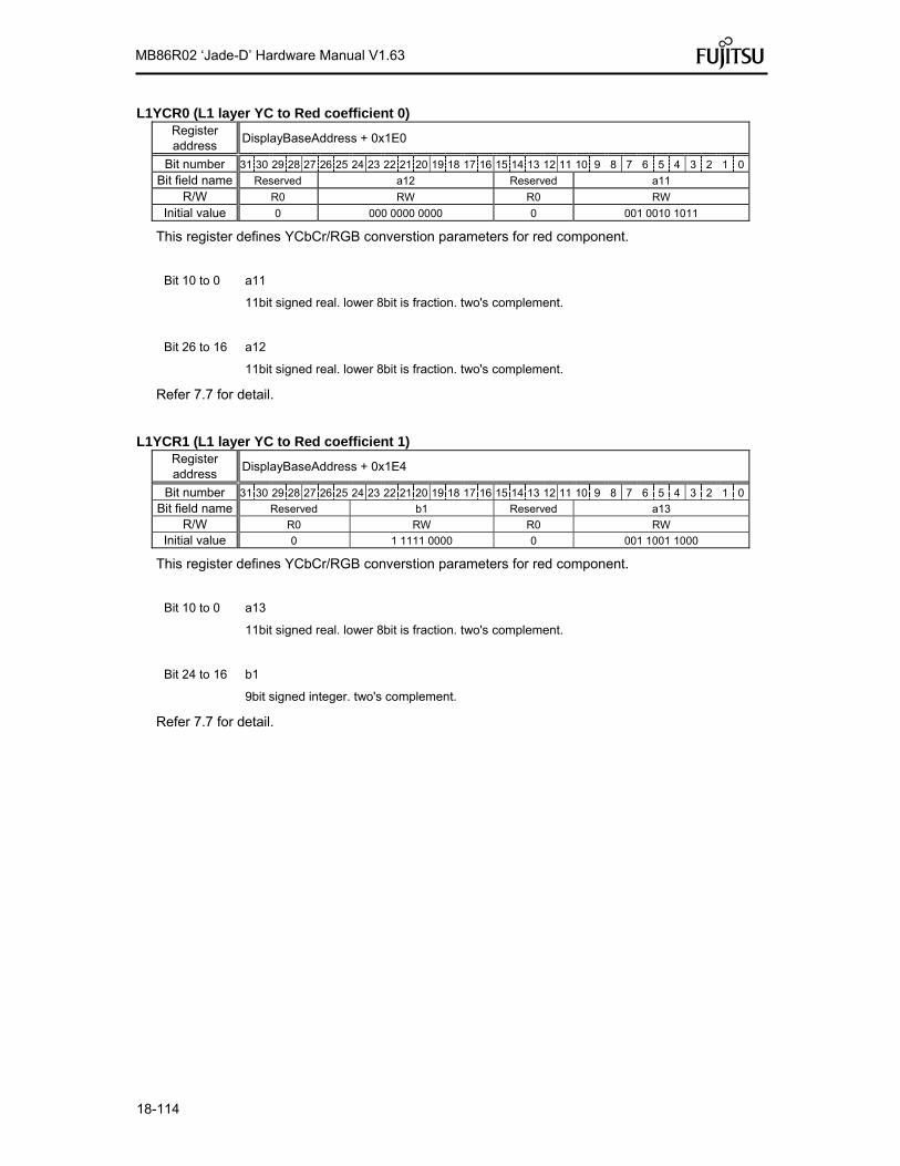
18-114
MB86R02 ‘Jade-D’ Hardware Manual V1.63
L1YCR0 (L1 layer YC to Red coefficient 0) Register address
DisplayBaseAddress + 0x1E0
Bit number 31 30 29 28 27 26 25 24 23 22 21 20 19 18 17 16 15 14 13 12 11 10 9 8 7 6 5 4 3 2 1 0
Bit field name Reserved a12 Reserved a11
R/W R0 RW R0 RW
Initial value 0 000 0000 0000 0 001 0010 1011
This register defines YCbCr/RGB converstion parameters for red component.
Bit 10 to 0 a11
11bit signed real. lower 8bit is fraction. two's complement.
Bit 26 to 16 a12
11bit signed real. lower 8bit is fraction. two's complement.
Refer 7.7 for detail.
L1YCR1 (L1 layer YC to Red coefficient 1) Register address
DisplayBaseAddress + 0x1E4
Bit number 31 30 29 28 27 26 25 24 23 22 21 20 19 18 17 16 15 14 13 12 11 10 9 8 7 6 5 4 3 2 1 0
Bit field name Reserved b1 Reserved a13
R/W R0 RW R0 RW
Initial value 0 1 1111 0000 0 001 1001 1000
This register defines YCbCr/RGB converstion parameters for red component.
Bit 10 to 0 a13
11bit signed real. lower 8bit is fraction. two's complement.
Bit 24 to 16 b1
9bit signed integer. two's complement.
Refer 7.7 for detail.

18-115
MB86R02 ‘Jade-D’ Hardware Manual V1.63
L1YCG0 (L1 layer YC to Green coefficient 0) Register address
DisplayBaseAddress + 0x1E8
Bit number 31 30 29 28 27 26 25 24 23 22 21 20 19 18 17 16 15 14 13 12 11 10 9 8 7 6 5 4 3 2 1 0
Bit field name Reserved a22 Reserved a21
R/W R0 RW R0 RW
Initial value 0 111 1001 1100 0 001 0010 1011
This register defines YCbCr/RGB converstion parameters for green component.
Bit 10 to 0 a21
11bit signed real. lower8bit is fraction. two's complement.
Bit 26 to 16 a22
11bit signed real. lower 8bit is fraction. two's complement.
Refer 7.7 for detail.
L1YCG1 (L1 layer YC to Green coefficient 1) Register address
DisplayBaseAddress + 0x1EC
Bit number 31 30 29 28 27 26 25 24 23 22 21 20 19 18 17 16 15 14 13 12 11 10 9 8 7 6 5 4 3 2 1 0
Bit field name Reserved b2 Reserved a23
R/W R0 RW R0 RW
Initial value 0 1 1111 0000 0 111 0010 1111
This register defines YCbCr/RGB converstion parameters for green component.
Bit 10 to 0 a23
11bit signed real. lower 8bit is fraction. two's complement.
Bit 24 to 16 b2
9bit signed integer. two's complement.
Refer 7.7 for detail.

18-116
MB86R02 ‘Jade-D’ Hardware Manual V1.63
L1YCB0 (L1 layer YC to Blue coefficient 0) Register address
DisplayBaseAddress + 0x1F0
Bit number 31 30 29 28 27 26 25 24 23 22 21 20 19 18 17 16 15 14 13 12 11 10 9 8 7 6 5 4 3 2 1 0
Bit field name Reserved a32 Reserved a31
R/W R0 RW R0 RW
Initial value 0 010 0000 0100 0 001 0010 1011
This register defines YCbCr/RGB converstion parameters for blue component.
Bit 10 to 0 a31
11bit signed real. lower 8bit is fraction. two's complement.
Bit 26 to 16 a32
11bit signed real. lower 8bit is fraction. two's complement.
Refer 7.7 for detail.
L1YCB1 (L1 layer YC to Blue coefficient 1) Register address
DisplayBaseAddress + 0x1F4
Bit number 31 30 29 28 27 26 25 24 23 22 21 20 19 18 17 16 15 14 13 12 11 10 9 8 7 6 5 4 3 2 1 0
Bit field name Reserved b3 Reserved a33
R/W R0 RW R0 RW
Initial value 0 1 1111 0000 0 000 0000 0000
This register defines YCbCr/RGB converstion parameters for blue component.
Bit 10 to 0 a33
11bit signed real. lower 8bit is fraction. two's complement.
Bit 24 to 16 b3
9bit signed integer. two's complement.
Refer 7.7 for detail.

18-117
MB86R02 ‘Jade-D’ Hardware Manual V1.63
L0PAL0-255 (L0 layer Palette 0-255) Register address
DisplayBaseAddress + 0x400 ~ DisplayBaseAddress + 0x7FF
Bit number 31 30 29 28 27 26 25 24 23 22 21 20 19 18 17 16 15 14 13 12 11 10 9 8 7 6 5 4 3 2 1 0
Bit field name A R G B
R/W RW R0 RW R0 RW R0 RW R0
Initial value X 0000000 X 00 X 00 X 00
These are color palette registers for L0 layer and cursors. In the indirect color mode, a color code in the display frame indicates the palette register number and the color information set in that register is applied as the display color of that pixel. This register corresponds to the CPALn register for previous products.
Bit 7 to 2 B (Blue)
Sets blue color component
Bit 15 to 10 G (Green)
Sets green color component
Bit 23 to 18 R (Red)
Sets red color component
Bit 31 A (Alpha)
Specifies whether or not to perform blending with lower layers when the blending mode is enabled.
0 Blending not performed even when blending mode enabled
Overlay is performed via transparent color.
1 Blending performed

18-118
MB86R02 ‘Jade-D’ Hardware Manual V1.63
L1PAL0-255 (L1 layer Palette 0-255) Register address
DisplayBaseAddress + 0x800 ~ DisplayBaseAddress + 0xBFF
Bit number 31 30 29 28 27 26 25 24 23 22 21 20 19 18 17 16 15 14 13 12 11 10 9 8 7 6 5 4 3 2 1 0
Bit field name A R G B
R/W RW R0 RW R0 RW R0 RW R0
Initial value X 0000000 X 00 X 00 X 00
These are color palette registers for L1 layer and cursors. In the indirect color mode, a color code in the display frame indicates the palette register number and the color information set in that register is applied as the display color of that pixel. This register corresponds to the MBPALn register for previous products.
Bit 7 to 2 B (Blue)
Sets blue color component
Bit 15 to 10 G (Green)
Sets green color component
Bit 23 to 18 R (Red)
Sets red color component
Bit 31 A (Alpha)
Specifies whether or not to perform blending with lower layers when the blending mode is enabled.
0 Blending not performed even when blending mode enabled
Overlay is performed via transparent color.
1 Blending performed

18-119
MB86R02 ‘Jade-D’ Hardware Manual V1.63
L2PAL0-255 (L2 layer Palette 0-255) Register address
DisplayBaseAddress + 0x1000 ~ DisplayBaseAddress + 0x13FF
Bit number 31 30 29 28 27 26 25 24 23 22 21 20 19 18 17 16 15 14 13 12 11 10 9 8 7 6 5 4 3 2 1 0
Bit field name A R G B
R/W RW R0 RW R0 RW R0 RW R0
Initial value X 0000000 X 00 X 00 X 00
These are color palette registers for L2 layer and cursors. In the indirect color mode, a color code in the display frame indicates the palette register number and the color information set in that register is applied as the display color of that pixel.
Bit 7 to 2 B (Blue)
Sets blue color component
Bit 15 to 10 G (Green)
Sets green color component
Bit 23 to 18 R (Red)
Sets red color component
Bit 31 A (Alpha)
Specifies whether or not to perform blending with lower layers when the blending mode is enabled.
0 Blending not performed even when blending mode enabled
Overlay is performed via transparent color.
1 Blending performed

18-120
MB86R02 ‘Jade-D’ Hardware Manual V1.63
L3PAL0-255 (L3 layer Palette 0-255) Register address
DisplayBaseAddress + 0x1400 ~ DisplayBaseAddress + 0x17FF
Bit number 31 30 29 28 27 26 25 24 23 22 21 20 19 18 17 16 15 14 13 12 11 10 9 8 7 6 5 4 3 2 1 0
Bit field name A R G B
R/W RW R0 RW R0 RW R0 RW R0
Initial value X 0000000 X 00 X 00 X 00
These are color palette registers for L3 layer and cursors. In the indirect color mode, a color code in the display frame indicates the palette register number and the color information set in that register is applied as the display color of that pixel.
Bit 7 to 2 B (Blue)
Sets blue color component
Bit 15 to 10 G (Green)
Sets green color component
Bit 23 to 18 R (Red)
Sets red color component
Bit 31 A (Alpha)
Specifies whether or not to perform blending with lower layers when the blending mode is enabled.
0 Blending not performed even when blending mode enabled
Overlay is performed via transparent color.
1 Blending performed

18-121
MB86R02 ‘Jade-D’ Hardware Manual V1.63
18.7.10 Video capture registers
VCM (Video Capture Mode)
Register address CaptureBaseAddress + 0x00
Bit number 31 30 29 28 27 26 25 24 23 22 21 20 19 18 17 16 15 14 --- 5 4 3 2 1 0
Bitfield name VIE
VIS
rese
rve
VIC
E
rese
rve
CM Reserve VI reserve
NR
GB
VS
rese
rve
RW RW RW RX RW RW RW RX RW RX RW RW RX
Initial value 0 0 X 0 X 00 X 0 X 0 0 X
This register sets the video capture mode. This register is not initialized by software reset.
Bit1 VS (Video Select) NTSC or PAL is selected for the code error detection. (only the RTB656 is input.) 0 NTSC 1 PAL Bit2 NRGB(Native RGB input on) Native RGB mode is set up. 0 RGB video data is accepted via an internal RGB preprocessor which converts RGB to
YUV422 1 Native RGB
Bit20 VI (Vertical Interpolation) Sets whether to perform vertical interpolation 0 Performs vertical interpolation. The graphics are enlarged vertically by two times 1 Does not perform vertical interpolation Bit25-24 CM (Capture Mode) Sets video capture mode. To capture vides, set these bits to “11”. 00 Initial value 01 Reserved 10 Reserved 11 Capture Bit28 VICE (Video Input Clock Enable) Capture clock enable 0 Enable 1 Disable Bit30 VIS(Video Input Select) 0 RBT656/601 1 RGB Bit31 VIE (Video Input Enable) Enables video capture function 0 Does not capture video 1 Captures video
-Procedure of video capture clock Stop-
1) 0 is written in bit31 (VIE) of the VCM register and the video capture function is invalidated.
2) 1 is written in bit28 (VICE) of the VCM register and Stop does video capture clock.
-Procedure of video capture clock beginning-
1) 0 is written in bit28 (VICE) of the VCM register and video capture clock is made effective.

18-122
MB86R02 ‘Jade-D’ Hardware Manual V1.63
2) 1 is written in bit31 (VIE) of the VCM register and the video capture function is made effective.

18-123
MB86R02 ‘Jade-D’ Hardware Manual V1.63
CSC (Capture SCale) Register address CaptureBaseAddress + 04h
Bit number 31 30 29 28 27 26 25 24 23 22 21 20 19 18 17 16 15 14 13 12 11 10 9 8 7 6 5 4 3 2 1 0 Bit field name VSCI VSCF HSCI HSCF
R/W R/W R/W R/W R/W Initial value 00001 00000000000 00001 00000000000
This register sets the video capture upscaling/downscaling ratio.
Bit10-0 HSCF (Vertical SCale Fraction) The decimal part of a horizontal upscaling/downscaling ratio is set. Bit15-11 HSCI (Horizontal Scale Integer) The integer part of a horizontal upscaling/downscaling ratio is set. Bit26-16 VSCF (Vertical SCale Fraction) The decimal part of a vertical upscaling/downscaling ratio is set. Bit31-27 VSCI (Vertical SCale Integer) The integer part of a vertical upscaling/downscaling ratio is set.
Note: Smooth continuation operation to Down Scaling mode and Up Scaling mode cannot be performed. The picture disorder of some arises at the time of a change. This is the restrictions for Up Scaling mode and Down Scaling mode using the same interpolate circuit.
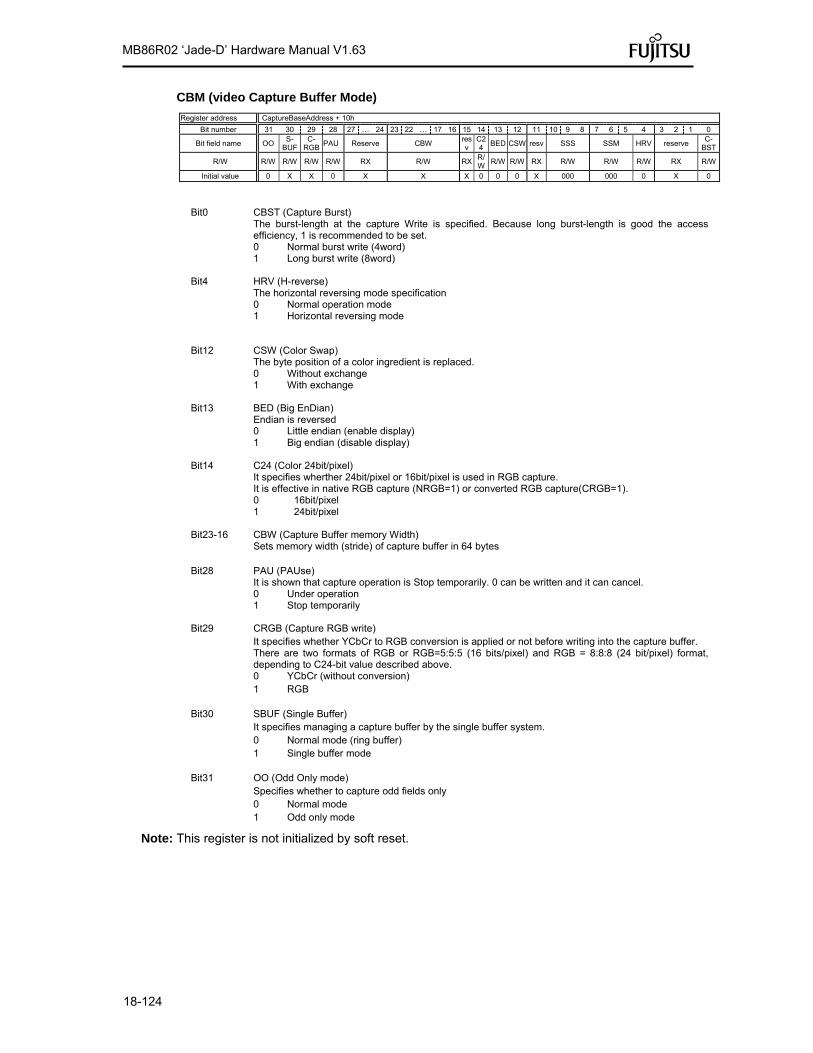
18-124
MB86R02 ‘Jade-D’ Hardware Manual V1.63
CBM (video Capture Buffer Mode)
Register address CaptureBaseAddress + 10h
Bit number 31 30 29 28 27 … 24 23 22 … 17 16 15 14 13 12 11 10 9 8 7 6 5 4 3 2 1 0
Bit field name OO S-
BUF C-
RGB PAU Reserve CBW
resv
C24
BED CSW resv SSS SSM HRV reserve C-
BST
R/W R/W R/W R/W R/W RX R/W RXR/W
R/W R/W RX R/W R/W R/W RX R/W
Initial value 0 X X 0 X X X 0 0 0 X 000 000 0 X 0
Bit0 CBST (Capture Burst) The burst-length at the capture Write is specified. Because long burst-length is good the access
efficiency, 1 is recommended to be set. 0 Normal burst write (4word) 1 Long burst write (8word)
Bit4 HRV (H-reverse) The horizontal reversing mode specification
0 Normal operation mode 1 Horizontal reversing mode
Bit12 CSW (Color Swap)
The byte position of a color ingredient is replaced. 0 Without exchange
1 With exchange Bit13 BED (Big EnDian)
Endian is reversed 0 Little endian (enable display)
1 Big endian (disable display) Bit14 C24 (Color 24bit/pixel) It specifies wherther 24bit/pixel or 16bit/pixel is used in RGB capture.
It is effective in native RGB capture (NRGB=1) or converted RGB capture(CRGB=1). 0 16bit/pixel 1 24bit/pixel Bit23-16 CBW (Capture Buffer memory Width)
Sets memory width (stride) of capture buffer in 64 bytes
Bit28 PAU (PAUse) It is shown that capture operation is Stop temporarily. 0 can be written and it can cancel.
0 Under operation 1 Stop temporarily
Bit29 CRGB (Capture RGB write) It specifies whether YCbCr to RGB conversion is applied or not before writing into the capture buffer.
There are two formats of RGB or RGB=5:5:5 (16 bits/pixel) and RGB = 8:8:8 (24 bit/pixel) format, depending to C24-bit value described above.
0 YCbCr (without conversion) 1 RGB
Bit30 SBUF (Single Buffer) It specifies managing a capture buffer by the single buffer system. 0 Normal mode (ring buffer) 1 Single buffer mode
Bit31 OO (Odd Only mode) Specifies whether to capture odd fields only 0 Normal mode 1 Odd only mode
Note: This register is not initialized by soft reset.
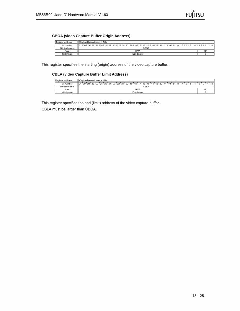
18-125
MB86R02 ‘Jade-D’ Hardware Manual V1.63
CBOA (video Capture Buffer Origin Address)
Register address CaptureBaseAddress + 14h
Bit number 31 30 29 28 27 26 25 24 23 22 21 20 19 18 17 16 15 14 13 12 11 10 9 8 7 6 5 4 3 2 1 0 Bit field name CBOA
R/W R/W R0 Initial value Don’t care 0
This register specifies the starting (origin) address of the video capture buffer. CBLA (video Capture Buffer Limit Address)
Register address CaptureBaseAddress + 18h
Bit number 31 30 29 28 27 26 25 24 23 22 21 20 19 18 17 16 15 14 13 12 11 10 9 8 7 6 5 4 3 2 1 0 Bit field name CBLA
R/W R/W R0 Initial value Don’t care 0
This register specifies the end (limit) address of the video capture buffer.
CBLA must be larger than CBOA.

18-126
MB86R02 ‘Jade-D’ Hardware Manual V1.63
CIHSTR (Capture Image Horizontal STaRt)
Register address CaptureBaseAddress + 1Ch
Bit number 15 14 13 12 11 10 9 8 7 6 5 4 3 2 1 0
Bit field name Reserved CIHSTR R/W RX R/W
Initial value Don’t care Don’t care
This register sets the range of the images to be written (captured) to the video capture buffer. Specify the X coordinates located in the top left of the image range as the count of pixels from the top left of the image. For downscaling, apply this setting to the post-reduction image coordinates.
-Note: The even number is set at the YUV mode. CIVSTR (Capture Image Vertical STaRt)
Register address CaptureBaseAddress + 1Eh
Bit number 15 14 13 12 11 10 9 8 7 6 5 4 3 2 1 0
Bit field name Reserved CIVSTR R/W RX R/W
Initial value Don’t care Don’t care
This register sets the range of the images to be written (captured) to the video capture buffer. Specify the Y coordinates located in the top left of the image range as the count of pixels from the top left of the image. For downscaling, apply this setting to the post-reduction image coordinates.

18-127
MB86R02 ‘Jade-D’ Hardware Manual V1.63
CIHEND (Capture Image Horizontal END)
Register address CaptureBaseAddress + 20h
Bit number 15 14 13 12 11 10 9 8 7 6 5 4 3 2 1 0
Bit field name Reserved CIHEND R/W RX R/W
Initial value X X
This register sets the range of the images to be written (captured) to the video capture buffer. Specify the X coordinates located in the bottom right of the image range as the count of pixels from the top left of the image. For downscaling, apply this setting to the post-reduction image coordinates.
If the pixel at the right end of the image is not aligned on 64 bits/word boundary, extra data is written before 64 bits/word boundary.
If the width of the input image is less than the range set by this command, data is written only at the size of input image.
-Note: In the YUV mode, horizontal pixel size (CIHEND-CIHSTR) sets the even number. CIVEND (Capture Image Vertical END)
Register address CaptureBaseAddress + 22h
Bit number 15 14 13 12 11 10 9 8 7 6 5 4 3 2 1 0
Bit field name Reserved CIVEND R/W RX R/W
Initial value X X
This register sets the range of the images to be written (captured) to the video capture buffer. Specify the Y coordinates located in the bottom right of the image range as the count of pixels from the top left of the original image to be input. For downscaling, apply this setting to the post-reduction image coordinates.
If the count of rasters of the input image is less than the range set by this command, data is written only at the size of the input image.
CVCNT (Capture Vertical Count)
Register address CaptureBaseAddress + 300h
Bit number 15 14 13 12 11 10 9 8 7 6 5 4 3 2 1 0 Bit field name Reserved CVCNT
R/W R0 R Initial value 0 Don’t care
Y coordinates of the raster which is carrying out the capture are shown. Only read-out is possible.

18-128
MB86R02 ‘Jade-D’ Hardware Manual V1.63
CHP (Capture Horizontal Pixel)
Register address CaptureBaseAddress + 28h
Bit number 31 30 29 28 27 26 25 24 23 22 21 20 19 18 17 16 15 14 13 12 11 10 9 8 7 6 5 4 3 2 1 0 Bit field name Reserved CHP
R/W RX R/W Initial value X 0x168 (360)
This register sets the count of horizontal pixels of the image output after scaling. Specify the count of horizontal pixels in 2 pixels. Maximum is 840 pixels (setting value is 0x1A4)
CVP (Capture Vertical Pixel) Register address
CaptureBaseAddress + 2cH
Bit number 31 30 29 28 27 26 25 24 23 22 21 20 19 18 17 16 15 14 13 12 11 10 9 8 7 6 5 4 3 2 1 0
Bit field name Reserved CVPP Reserved CVPN
R/W RX RW RX RW
Initial value X 271H (625D) X 20DH (525D)
This register sets the count of vertical pixels of the image output after scaling. The fields to be used depend on the video format to be used.
Bit 25 to 16 CVPP (Capture Vertical Pixel for PAL)
Set count of vertical pixels of output image in PAL format used
Bit 9 to 0 CVPN (Capture Vertical Pixel for NTSC)
Set count of vertical pixels of output image in NTSC format used

18-129
MB86R02 ‘Jade-D’ Hardware Manual V1.63
CLPF (Capture Low Pass Filter) Register address CaptureBaseAddress + 40h
Bit number 31 30 29 28 27 26 25 24 23 22 21 20 19 18 17 16 15 14 13 12 11 10 9 8 7 6 5 4 3 2 1 0 Bit field name Reserved CVLPF Reserved CHLPF Reserved
R/W RX R/W RX R/W RX Initial value 0 0 0 0 X
This register sets the Low Pass Filter Coefficient. The vertical low pass filter consists of FIR filters of three taps. The horizontal low pass filter consists of FIR filters of five taps. It specifies independently in 2-bit coefficient code with a luminance signal (Y) and a chrominance signal (Cb and Cr) . A low pass filter is OFF (through) in a setup of each coefficient code “00”.
Bit 17 to 16 CHLPF_C (Capture Horizontal LPF coefficient C)
CHLPF_C K0 K1 K2 K3 K4
00 0 0 1 0 0
01 0 1/4 2/4 1/4 0
10 0 3/16 10/16 3/16 0
11 3/32 8/32 10/32 10/32 3/32
Bit 19 to 18 CHLPF_Y (Capture Horizontal LPF coefficient Y)
CHLPF_Y K0 K1 K2 K3 K4
00 0 0 1 0 0
01 0 1/4 2/4 1/4 0
10 0 3/16 10/16 3/16 0
11 3/32 8/32 10/32 10/32 3/32
Bit 25 to 24 CVLPF_C (Capture Vertical LPF coefficient C)
CVLPF_C K0 K1 K2
00 0 1 0
01 1/4 2/4 1/4
10 3/16 10/16 3/16
11 Reserved
Bit 27 to 26 CVLPF_Y (Capture Vertical LPF coefficient Y)
CVLPF_Y K0 K1 K2
00 0 1 0
01 1/4 2/4 1/4
10 3/16 10/16 3/16
11 Reserved
Note: In the case of Native RGB mode (NRGB=1), only a setup of CVLPF_Y code becomes effective.
CMSS (Capture Magnify Source Size)
Register address CaptureBaseAddress + 48h
Bit number 31 30 29 28 27 26 25 24 23 22 21 20 19 18 17 16 15 14 13 12 11 10 9 8 7 6 5 4 3 2 1 0 Bit field name Reserved CMSHP Reserved CMSVL
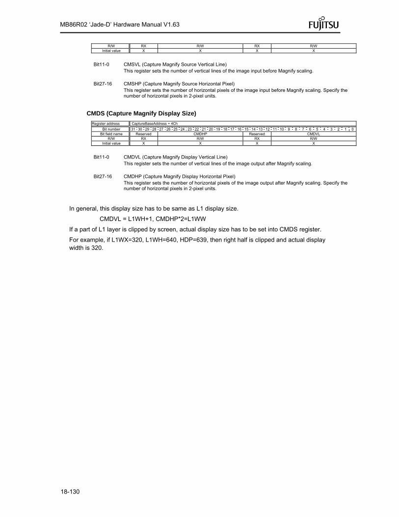
18-130
MB86R02 ‘Jade-D’ Hardware Manual V1.63
R/W RX R/W RX R/W Initial value X X X X
Bit11-0 CMSVL (Capture Magnify Source Vertical Line) This register sets the number of vertical lines of the image input before Magnify scaling. Bit27-16 CMSHP (Capture Magnify Source Horizontal Pixel) This register sets the number of horizontal pixels of the image input before Magnify scaling. Specify the
number of horizontal pixels in 2-pixel units.
CMDS (Capture Magnify Display Size)
Register address CaptureBaseAddress + 4Ch
Bit number 31 30 29 28 27 26 25 24 23 22 21 20 19 18 17 16 15 14 13 12 11 10 9 8 7 6 5 4 3 2 1 0 Bit field name Reserved CMDHP Reserved CMDVL
R/W RX R/W RX R/W Initial value X X X X
Bit11-0 CMDVL (Capture Magnify Display Vertical Line) This register sets the number of vertical lines of the image output after Magnify scaling. Bit27-16 CMDHP (Capture Magnify Display Horizontal Pixel) This register sets the number of horizontal pixels of the image output after Magnify scaling. Specify the
number of horizontal pixels in 2-pixel units.
In general, this display size has to be same as L1 display size.
CMDVL = L1WH+1, CMDHP*2=L1WW
If a part of L1 layer is clipped by screen, actual display size has to be set into CMDS register.
For example, if L1WX=320, L1WH=640, HDP=639, then right half is clipped and actual display width is 320.

18-131
MB86R02 ‘Jade-D’ Hardware Manual V1.63
RGBHC(RGB input Hsync Cycle)
Register address CaptureBaseAddress + 80h
Bit number 31 30 29 28 27 26 25 24 23 22 21 20 19 18 17 16 15 14 13 12 11 10 9 8 7 6 5 4 3 2 1 0 Bit field name Reserved RGBHC
R/W RX R/W Initial value X X
Bit13-0 RGBHC
This register sets number of HSYNC cycles of the RGB input. . It is used when it is made a setup which samples VSYNC. The setting value +1 is a level cycle.
RGBHEN(RGB input Horizontal Enable area)
Register address CaptureBaseAddress + 84h
Bit number 31 30 29 28 27 26 25 24 23 22 21 20 19 18 17 16 15 14 13 12 11 10 9 8 7 6 5 4 3 2 1 0 Bit field name Reserved RGBHST Reserved RGBHEN
R/W RX R/W RX R/W Initial value X X X X
It is a parameter for determining effective pixel data.
Bit12-0 RGBHEN(RGB input Horizontal Enable area Size) Effective pixel data size is set up per pixel. Specify the number of horizontal pixels in 2-pixel units Bit27-16 RGBHST(RGB input Horizontal Enable area Start position) The start position of effective pixel data is set up. The setting value -4 is a start position.
Note: The maximum horizontal enable area size(RGBHEN) which can be captured is 840 pixels. This is the restriction by line buffer size in a video capture module.
RGBVEN(RGB input Vertical Enable area)
Register address CaptureBaseAddress + 88h
Bit number 31 30 29 28 27 26 25 24 23 22 21 20 19 18 17 16 15 14 13 12 11 10 9 8 7 6 5 4 3 2 1 0
Bit field name Reserv
ed Reserved RGBVST Reserved RGBVEN
R/W RX R/W R/W RX R/W Initial value X X X X X
It is a parameter for determining effective pixel data.
Bit12-0 RGBVEN(RGB input Vertical Enable area Size) Set effective line size
Bit24-16 RGBVST(RGB input Vertical Enable area Start position) The start position of effective line is set up. The setting value -1 is a start position.

18-132
MB86R02 ‘Jade-D’ Hardware Manual V1.63
RGBS (RGB input Sync)
Register address CaptureBaseAddress + 90h
Bit number 31 30 29 28 27 26 25 24 23 22 21 20 19 18 17 16 15 14 13 12 11 10 9 8 7 6 5 4 3 2 1 0 Bit field name Reserved RM Reserved HP VP
R/W RX R/W
RX R/W
R/W
Initial value X 1 X 0 0
Edge detection of a synchronized signal is set up. It is used at the time of RGB input format.
Bit0 VP (VSYNCI Polarity) 0 Negative edge of VINVSYNC is set to VSYNC. 1 Positive edge of VINVSYNC is set to VSYNC. Bit1 HP (HSYNCI Polarity) 0 Negative edge of VINHSYNC is set to HSYNC.
1 Positive edge of VINHSYNC is set to HSYNC.
Bit16 RM(RGB Input Mode select)
Sets Direct RGB input mode 0 reserved 1 RGB666 Direct input Mode

18-133
MB86R02 ‘Jade-D’ Hardware Manual V1.63
Conversion Operation
RGB data is converted to YUV by the following matrix expression :
Y = a11R + a12G + a13B + b1
Cb= a21R + a22G + a23B + b2 aij : 10bit signed real (lower 8bit is fraction)
Cr= a31R + a32G + a33B + b3 bi : 8bit unsigned integer
Each coefficients can be defined by following registers.
Cb and Cr components are reduced half after this operation to form the 4:2:2 format.
RGBCMY (RGB Color convert Matrix Y coefficient) Register address
CaptureBaseAddress + C0H
Bit number 31 30 29 28 27 26 25 24 23 22 21 20 19 18 17 16 15 14 13 12 11 10 9 8 7 6 5 4 3 2 1 0
Bit field name a11 Re a12 Re a13
R/W RW R RW R RW
Initial value 0001000010 b 0 0010000000 b 0 0000011001 b
This register sets the RGB color convert matrix coefficient.
Bit 31 to 22 a11
10bit signed real (lower8bit is fraction)
Bit 20 to 11 a12
10bit signed real (lower8bit is fraction)
Bit 9 to 0 a13
10bit signed real (lower8bit is fraction)
RGBCMCb (RGB Color convert Matrix Cb coefficient) Register address
CaptureBaseAddress + C4H
Bit number 31 30 29 28 27 26 25 24 23 22 21 20 19 18 17 16 15 14 13 12 11 10 9 8 7 6 5 4 3 2 1 0
Bit field name a21 Re a22 Re a23
R/W RW R RW R RW
Initial value 1111011010 b 0 1110110110 b 0 0001110000 b
This register sets the RGB color convert matrix coefficient.
Bit 31 to 22 A21
10bit signed real (lower8bit is fraction)
Bit 20 to 11 A22
10bit signed real (lower8bit is fraction)
Bit 9 to 0 A23

18-134
MB86R02 ‘Jade-D’ Hardware Manual V1.63
10bit signed real (lower8bit is fraction)
RGBCMCr (RGB Color convert Matrix Cr coefficient) Register address
CaptureBaseAddress + C8H
Bit number 31 30 29 28 27 26 25 24 23 22 21 20 19 18 17 16 15 14 13 12 11 10 9 8 7 6 5 4 3 2 1 0
Bit field name A31 Re A32 Re A33
R/W RW R RW R RW
Initial value 0001110000 b 0 1110100010 b 0 1111101110 b
This register sets the RGB color convert matrix coefficient.
Bit 31 to 22 A31
10bit signed real (lower8bit is fraction)
Bit 20 to 11 A32
10bit signed real (lower8bit is fraction)
Bit 9 to 0 A33
10bit signed real (lower8bit is fraction)
RGBCMb (RGB Color convert Matrix b coefficient) Register address
CaptureBaseAddress + CCH
Bit number 31 30 29 28 27 26 25 24 23 22 21 20 19 18 17 16 15 14 13 12 11 10 9 8 7 6 5 4 3 2 1 0
Bit field name R B1 Res b2 Res b3
R/W R RW R RW R RW
Initial value 0 000010000 b 0 010000000 b 0 010000000 b
This register sets the RGB color convert matrix coefficient.
Bit 30 to 22 B1
9bit unsigned integer
Bit 19 to 11 B2
9bit unsigned integer
Bit 8 to 0 B3
9bit unsigned integer

18-135
MB86R02 ‘Jade-D’ Hardware Manual V1.63
【656 Code error detect】 < RBT656 format input only>
CDCN (Capture Data Count for NTSC)
Register address CaptureBaseAddress + 4000h
Bit number 31 30 29 28 27 26 25 24 23 22 21 20 19 18 17 16 15 14 13 12 11 10 9 8 7 6 5 4 3 2 1 0 Bit field name Reserved BDCN Reserved VDCN
R/W RX RW RX RW Initial value X 0x10f(271) X 0x5A3(1443)
This register sets the count of data of the input video stream in NTSC format.
Bit12-0 VDCN (Valid Data Count for NTSC)
Sets count of data processed during valid period in NTSC format. The setting value +1 is a data number
Bit28-16 BDCN (Blanking Data Count for NTSC) Sets count of data processed during blanking period in NTSC format. The setting value +1 is a data
number
The range of VDCN and BDCN is shown in the following figure.
SAV: start of active video timing reference code EAV: end of active video timing reference code T: clock period 37 ns nom.
SAVEAV Multiplexed video data
Cb,Y,Cr,Y,Cb,Y,Cr,Y,….. VI[7:0]
4T
H-BLANK 276T 525
ACTIVE-VIDEO 1440T [525]
EAV
4T
Blanking data
80,10,80,10,80,.
4T
288T 625
272T(BDCN:271T) 284T(BDCP:283T)
1444T(VDCN:1443T) 1444T(VDCP:1443T)
1440T [625]

18-136
MB86R02 ‘Jade-D’ Hardware Manual V1.63
CDCP (Capture Data Count for PAL)
Register address CaptureBaseAddress + 4004h
Bit number 31 30 29 28 27 26 25 24 23 22 21 20 19 18 17 16 15 14 13 12 11 10 9 8 7 6 5 4 3 2 1 0 Bit field name Reserved BDCP Reserved VDCP
R/W RX RW RX RW Initial value X 0x11B(283) X 0x5A3(1443)
This register sets the count of data of the input video stream in PAL format.
Bit12-0 VDCP (Valid Data Count for PAL) Sets count of data processed during valid period in PAL format. The setting value +1 is a data
number Bit28-16 BDCP (Blanking Data Count for PAL) Sets count of data processed during blanking period in PAL format. The setting value +1 is a data
number

18-137
MB86R02 ‘Jade-D’ Hardware Manual V1.63
VCS (Video Capture Status)
Register address CaptureBaseAddress + 08h
Bit number 31 30 29 28 27 26 25 24 23 22 21 20 19 18 17 16 15 14 13 12 11 10 9 8 7 6 5 4 3 2 1 0 Bit field name Reserve CE
R/W RX RW0 Initial value X 00000
This register indicates the ITU-RBT656 SAV and EAV status. To detect error codes, set NTSC/PAL in the VS bit of VCM. If NTSC is set, reference the number of data in the capture data count register (CDCN). If PAL is set, reference the number of data in the capture data counter register (CDCP). If the reference data does not match the stream data , or undefined Fourth word of SAV/EAV codes are detected, bits 4 to 0 of the video capture status register (VCS) will be values as follows.
Bits 6-0 CE0 (Capture Error 0) Bit0 1 : RBT.656 undefined error (Code Bit7) 0 : true Bit1 1 : RBT.656 undefined error (Code Bit7-4) 0 : true Bit2 1 : RBT.656 undefined error (Code Bit7-0) 0 : true Bit3 1 : RBT.656 long term H code error (SAV) 0 : true Bit4 1 : RBT.656 long term H code error (EAV) 0 : true

18-138
MB86R02 ‘Jade-D’ Hardware Manual V1.63
18.8 Timing Diagrams
18.8.1 Display Timing Diagram
18.8.1.1 Non-interlace mode
VDP+1 rasters
VSYNC
HSYNC
VSP+1 rasters
VTR+1 rasters
VSW+1 rasters
HDP+1 clocks
HSP+1 clocks
HTP+1 clocks
HSW+1 clocks
HSYNC
RiGiBi
Assert Frame Interrupt
Assert Vsync Interrupt
Latency 13 clocks
DISPE
Ri/Gi/Bi
DISPE
DCLKO
0 1 2 n1n2 n=HDP+1
Ri/Gi/Bi
Non-interlace Timing
In the above diagram, VTR, HDP, etc., are the setting values of their associated registers.
The VSYNC/frame interrupt is asserted when display of the last raster ends. When updating display parameters, synchronize with the frame interrupt so no display disturbance occurs. Calculation for the next frame is started immediately after the vertical synchronization pulse is asserted, so the parameters must be updated by the time that calculation is started.

18-139
MB86R02 ‘Jade-D’ Hardware Manual V1.63
VSYNC is output 1 dot clock faster than HSYNC.

18-140
MB86R02 ‘Jade-D’ Hardware Manual V1.63
18.8.1.2 Interlace video mode
VDP+1 rasters
VSYNC
HSYNC
VSP+1 rasters
VTR+1 rasters (odd field)
VSW+1 rasters
VTR+1 rasters (even field)
VSW+1 rasters
VSYNC
HSYNC
VDP+1 rasters
VSP+1 rasters
Assert Vsync Interrupt
Assert Vsync Interrupt
Assert Frame Interrupt
Ri/Gi/Bi
Ri/Gi/Bi
Interlace Video Timing
In the above diagram, VTR, HDP, etc., are the setting values of their associated registers.
The interlace mode also operates at the same timing as the interlace video mode. The only difference between the two modes is the output image data.

18-141
MB86R02 ‘Jade-D’ Hardware Manual V1.63
18.8.2 Composite synchronous signal
When the EEQ bit of the DCM register is “0”, the CSYNC signal output waveform is as shown below.
Fig 11.12 Composite Synchronous Signal without Equalizing Pulse
When the EEQ bit of the DCM register is “1”, the equalizing pulse is inserted into the CSYNC signal, producing the waveform shown below.
Fig 11.13 Composite Synchronous Signal with Equalizing Pulse
The equalizing pulse is inserted when the vertical blanking time period starts. It is also inserted three times after the vertical synchronization time period has elapsed.
CSYNC
VSYNC
CSYNC
VSYNC
odd field
even field odd field
even field
CSYNC
VSYNC
CSYNC
VSYNC
odd field
even field odd field
even field

18-142
MB86R02 ‘Jade-D’ Hardware Manual V1.63
18.9 Geometry Engine
18.9.1 Geometry Pipeline
18.9.1.1 Processing flow
The flow of geometry is shown below.
Calculation is done by “32bit integer”,”32bit fixed-point-integer” or “32bit floating-point”. There is a limitation by itself. And algorithm also has limitation. Not all possible parameter or data can proceed correctly.
Object coordinates (OC)
Clip coordinates (CC)
Normalized device coordinates (NDC)
Drawing (device) coordinates (DC)
MVP Transformation
Clipping
3D-2D Transformation
View port transformation
Back face culling

18-143
MB86R02 ‘Jade-D’ Hardware Manual V1.63
18.9.1.2 Model-view-projection (MVP) transformation
The geometry engine transforms the vertex of the “OC” coordinate system specified by the G_Vertex packet to the “CC” coordinate system according to the coordinate transformation matrix (OC CC Matrix) specified by the G_LoadMatrix packet. The “OC CC Matrix” is a “4 4” matrix consisting of a ModelView matrix and a Projection matrix.
If “Zoc” is not contained in the input parameter of the G_Vertex packet (Z-bit of GMDR0 is off), (OC CC) coordinate transformation is processed as “Zoc = 0”.
When GMDR0[0] is 0 (orthogonal projection transformation), OC CC coordinate transformation is processed as “Wcc = 1.0”. (Work only for C=0,Z=0 and ST=0 (XY only vertex) mode)
OC: Object Coordinates
CC: Clip Coordinates
Ma0 to Md3: OC CC Matrix
Xoc to Zoc: X, Y and Z of OC coordinate system
Xcc to Woc: X, Y, Z and W of CC coordinate system
18.9.1.3 3D-2D transformation (CCNDC coordinate transformation)
The geometry engine divides “XYZ” of the “CC” coordinate system by “Wcc” (Perspective Division).
NDC: Normalized Device Coordinates
Xndc to Zndc: X, Y and Z of “NDC” coordinate system
Ma0
Mb0
Mc0
Md0
Ma1
Mb1
Mc1
Md1
Ma2
Mb2
Mc2
Md2
Ma3
Mb3
Mc3
Md3
Xcc
Ycc
Zcc
Wcc
Xoc
Yoc
Zoc
1
Xndc
Yndc
Zndc
1/Wcc
Xcc
Ycc
Zcc

18-144
MB86R02 ‘Jade-D’ Hardware Manual V1.63
18.9.1.4 View port transformation (NDCDC coordinate transformation)
The geometry engine transforms “XYZ” of the “NDC” coordinate system to the “DC” coordinate system according to the transformation coefficient specified by G_ViewPort and G_DepthRange.
“X_Scaling,X_Offset” and “Y_Scaling,Y_Offset” are coefficients to be mapped finally to Frame Buffer. Xdc and Ydc must be included within the drawing input range (-4096 to 4095). “Z_Scaling” and “Z_Offset” are coefficients to be mapped finally to “Z Buffer”. “Zdc” must be included within the “Z Buffer” range (0 to 65535).
DC: Device Coordinates
Xdc = X_Scaling*Xndc + X_Offset
Ydc = Y_Scaling*Yndc + Y_Offset
Zdc = Z_Scaling*Zndc + Z_Offset
18.9.1.5 View volume clipping
Expression for determination
The expression for determining the MB86R02 'Jade-D' view volume clipping is shown below. W clipping is intended to prevent the overflow caused by 1/W.
Xmin*Wcc Xcc Xmax*Wcc
Ymin*Wcc Ycc Ymax*Wcc
Zmin*Wcc Zcc Zmax*Wcc
Wmin Wcc
Note: Xmin, Xmax, Ymin, Ymax, Zmin, Zmax and Wmin are the clip boundary values set by the G_ViewVolumeXYClip/ZClip/WClip packet.
Clipping-on/-off
View volume clipping-on/-off can be switched by using the clip boundary values set by the G_ViewVolumeXYClip/Zclip/WClip packet. To switch view volume clipping to off, set the maximum and minimum values of the geometry data format (IEEE single-precision floating point(*1)) in the “Clip.max” value(*2) and “Clip.min” value(*3), respectively. In this case, ‘All coordinate transformation results’ can be evaluated as within view volume range, making it possible to obtain the effect of view volume clipping-off.
This method is valid only when W clipping does not occur. When a clip boundary value (Wmin) that causes W clipping to occur is set, clipping is also performed for each clip area. Consequently, set an appropriate clip boundary value for Clip. Max value. and Clip. Min value., respectively.
If other values are set in “Clip.max” and Clip.min, view volume clipping-on operates. The coordinate transformation result is always compared with the values set in “Clip.max” and “Clip.min”.
*1: Maximum value = 0x7f7fffff, minimum value = 0xff7fffff
*2: Xmin,Ymin, Zmin, Wmin
*3: Xmax, Ymax, Zmax

18-145
MB86R02 ‘Jade-D’ Hardware Manual V1.63
An example of the G_ViewVolumeZclip packet is shown below.
0xf1012010 //Setting of GMDR0
0x00000000 //Data format: Floating point data format
0x45000000 //G_ViewVolumeZclip packet
0xff7fffff //Zmin.float setting value (minimum value of IEEE single-precision floating point)
0x7f7fffff //Zmax.float setting value (maximum value of IEEE single-precision floating point)
Example of G_ViewVolumeZclip Packet when Z Clipping Off
“W” clipping at orthogonal projection transformation
“W” at orthogonal projection transformation (GMDR0[0] = 0) is treated as “Wcc=1.0”. (Work only for C=0,Z=0 and ST=0 (XY only vertex) mode.)
For this reason, to suppress “W” clipping, the set “Wmin” value must be larger than 0 and 1.0 or less.
Relationship with drawing clip frame
For the following reasons, the clip boundary values of the view volume should be set so that the values after DC coordinate transformation will be larger than the drawing clip frame (2 pixels or more).
(1) “XY” on the view volume clip frame of the “CC” coordinate system may be drawn one pixel outside or inside the frame due to an operation error when it is finally mapped to the “DC” coordinate system.
(2) When the end point of a line overlaps the view volume frame mapped to the “DC” coordinate system, there are two cases, where the dots on the frame are drawn and not drawn depending on the specifying of the line drawing attribute (end point drawing/non-drawing).
(3) When the start point of a line overlaps the view volume frame mapped to the “DC” coordinate system, the dots on the frame are always drawn. When the line drawing attribute is ‘end point non-drawing,’ the dots on the frame are drawn at the starting point, but they may not be drawn at the end point.
(4) When applying to triangle and polygon drawing the rasterizing rule ‘dots containing center of pixel drawn. Dots on right side and base of triangle not drawn.’ depending on the value of the fraction, a gap may be produced between the right side and base of the frame.
Drawing clip frame
Drawing area
A space of two pixels or more is required.
“DC” Coordinates image of view volume clip frame

18-146
MB86R02 ‘Jade-D’ Hardware Manual V1.63
18.9.1.6 Back face culling
In MB86R02 'Jade-D', a triangle direction can be defined and a mode in which drawing for the back face is inhibited (back face culling) is supported. The on/off operation is controlled by the GMDR2[0] setting. GMDR2[0] must be set to 1 only when back face carling is required. When back face culling is not required such as in ‘line,’ ‘point,’ and ‘polygon primitive,’ GMDR2[0] must be set to 0.

18-147
MB86R02 ‘Jade-D’ Hardware Manual V1.63
18.9.2 Data Format
18.9.2.1 Data format
The supported data formats are 32-bit single-precision floating-point format, 32-bit fixed-point format, integer packed format and RGB packed format. All internal processing is performed in the floating-point format. For this reason, the integer packed format, fixed-point format and RGB packed format must be converted to the floating-point format. The processing speeds in these formats are slightly lower than in the 32-bit single-precision floating-point format.
The data format to use is selected by setting the GMDR0 register.
(1) 32-bit single-precision floating-point format 31 30 23 22 0
s e f
s: Sign bit (1 bit) e: Exponent part (8 bits) f: Mantissa (23 bits): ‘1.f’ shows the fraction. ‘1’ is a hidden bit.
The numerical value of the floating-point format becomes (-1)s(1.f)2(e-127) (0 < e < 255).
(2) Signed fixed-point format (SFIX16.16) 31 30 16 15 0
s Int Frac
s: Sign bit (1 bit) int: Integer (15 bits) frac: Fraction (16 bits)
(3) Signed integer packed format (SINT16.SINT16) 31 30 16 15 14 0
s Y.int s X.int
s: Sign bit (1 bit) int: Integer (15 bits)
(4) RGB packed format 31 24 23 16 15 8 7 0
reserved R G B
R, G, B: Color bits (8 bits)
(5) ARGB packed format 31 24 23 16 15 8 7 0
A R G B
A: Alpha bits (8 bits) R, G, B: Color bits (8 bits)

18-148
MB86R02 ‘Jade-D’ Hardware Manual V1.63
16.9.3. Setup Engine
18.9.2.2 Setup processing
The vertex data transformed by the geometry engine is transferred to the setup engine. MB86R02 'Jade-D' has a drawing interface that is compatible with the Coral PA. It operates parameters for various slope calculations, etc., with the setup engine. When the obtained parameters are set in the drawing engine, the final drawing processing starts.
18.9.3 Log Output of Device Coordinates
A function is provided to output device coordinates (DC) data obtained by view port conversion to local memory (graphics memory).
18.9.3.1 Log output mode
Drawing & log output command
Log output of drawing coordinates (device coordinates) can be performed concurrently with nclip_Points.int primitive drawing.
Log output can be controlled using the command with log output on/off attribute; log output is performed only when the log output on attribute is specified.
Log output dedicated command
When the log output dedicated command is used, log output of the device coordinates can be performed.
18.9.3.2 Log output destination address
The log output destination address is controlled by the device coordinates log pointer. Once set an address, this pointer automatically increment an output address.
18.9.3.3 Log output format
The log format consists of packed number of X and Y coordinates of vertex. bit
31 30 16 15 14 0 S Y S X
S : signed bit
Y:Y coordinates values (integer)
X:X coordinates values (integer

18-149
MB86R02 ‘Jade-D’ Hardware Manual V1.63
18.10 Drawing Processing
18.10.1 Coordinate System
18.10.1.1 Drawing coordinates
After the calculation of coordinates by the geometry engine, MB86R02 'Jade-D' draws data in the drawing frame in the graphics memory that finally uses the drawing coordinates (device coordinates).
Drawing frame is treated as 2D coordinates with the origin at the top left as shown in the figure below. The maximum coordinates is 4096 4096. Each drawing frame is located in the Graphics Memory by setting the address of the origin and resolution of X direction (size). Although the size of Y direction does not need to be set, Y coordinates which are max. at drawing must not be overlapped with other area. In addition, at drawing, specifying the clip frame (top left and bottom right coordinates) can prevent the drawing of images outside the clip frame.
X (max. 4096)
Y (
max
. 40
96)
Origin Drawing frame size X
Dra
win
g fr
ame
size
Y (Xmin, Ymin)
(Xmax, Ymax)
Clip frame

18-150
MB86R02 ‘Jade-D’ Hardware Manual V1.63
18.10.1.2 Texture coordinates
Texture coordinate is a 2D coordinate system represented as S and T (S: horizontal, T: vertical). Any integer in a range of 8192 to 8191 can be used as the S and T coordinates. The texture coordinates is correlated to the 2D coordinates of a vertex. One texture pattern can be applied to up to 4096 4096 pixels. The pattern size is set in the register. When the S and T coordinates exceed the maximum pattern size, the repeat, cramp or border color option is selected.
18.10.1.3 Frame buffer
For drawing, the following area must be assigned to the Graphics Memory. The frame size (count of pixels on X direction) is common for these areas.
Drawing frame
The results of drawing are stored in the graphical image data area. Both the direct and indirect color mode are applicable.
Z buffer
Z buffer is required for eliminating hidden surfaces. In 16 bits mode, 2 bytes and in 8 bits mode, 1 byte are required per 1 pixel.
Polygon drawing flag buffer
This area is used for polygon drawing. 1 bit is required per 1 pixel.
S (max. 8192)
T (
max
. 8
192)
Origin
max. 4096 pixels
max
. 40
96 p
ixel
s
Texture
pattern
18-151
MB86R02 ‘Jade-D’ Hardware Manual V1.63
18.10.2 Figure Drawing
18.10.2.1 Drawing primitives
MB86R02 'Jade-D' has a drawing interface that is compatible with the Coral PA graphics controller which does not perform geometry processing. The following types of figure drawing primitives are compatible with the MB86290A.
Point
Line
Triangle
High-speed 2DLine
High-speed 2DTriangle
Polygon
18.10.2.2 Polygon drawing function
An irregular polygon (including concave shape) is drawn by hardware in the following manner:
1. Execute PolygonBegin command.
Initialize polygon drawing hardware.
2. Draw vertices.
Draw outline of polygon and plot all vertices to polygon draw flag buffer using high-speed 2DTriangle primitive.
3. Execute PolygonEnd command.
Copy shape in polygon draw flag buffer to drawing frame and fill shape with color or specified tiling pattern.

18-152
MB86R02 ‘Jade-D’ Hardware Manual V1.63
18.10.2.3 Drawing parameters
The MB86290A-compatible interface uses the following parameters for drawing:
The triangles (Right triangle and Left triangle) are distinguished according to the locations of three vertices as follows (not used for high-speed 2DTriangle):
The following parameters are required for drawing triangles (for high-speed 2DTriangle, X and Y coordinates of each vertex are specified).
Note: Be careful about the positional relationship between coordinates Xs, XUs and XLs.
For example, in the above diagram, when a right-hand triangle is drawn using the parameter that shows the coordinates positional relationship Xs (upper edge start Y coordinates) > XUs or Xs (lower edge start Y coordinates) > XLs, the appropriate picture may not be drawn.
V0
Upper edge
Long edge
V1
Lower edgeV2
Upper triangle
Lower triangle
V1
V0
V2
Upper edge
Lower edge
Long edge Upper triangle
Lower triangle
Right-hand triangle Left-hand triangle
XUs
XLs
Ys Xs,Zs,Rs,Gs,Bs,Ss,Ts,Qs
Upper edge start Y coordinates
dXdy dZdy dRdy dGdy dBdy dSdy dTdy dQdy
dXUdy
dXLdy
Lower edge start Y coordinates
dZdx,dRdx,dGdx,dBdx,dSdx,dTdx,dQdx
USN
LSN
18-153
MB86R02 ‘Jade-D’ Hardware Manual V1.63
Ys Y coordinates start position of long edge in drawing triangle
Xs X coordinates start position of long edge corresponding to Ys
XUs X coordinates start position of upper edge
XLs X coordinates start position of lower edge
Zs Z coordinates start position of long edge corresponding to Ys
Rs R color value of long edge corresponding to Ys
Gs G color value of long edge corresponding to Ys
Bs B color value of long edge corresponding to Ys
Ss S coordinate of textures of long edge corresponding to Ys
Ts T coordinate of textures of long edge corresponding to Ys
Qs Q perspective correction value of texture of long edge corresponding to Ys
dXdy X DDA value of long edge direction
dXUdy X DDA value of upper edge direction
dXLdy X DDA value of lower edge direction
dZdy Z DDA value of long edge direction
dRdy R DDA value of long edge direction
dGdy G DDA value of long edge direction
dBdy B DDA value of long edge direction
dSdy S DDA value of long edge direction
dTdy T DDA value of long edge direction
dQdy Q DDA value of long edge direction
USN Count of spans of upper triangle
LSN Count of spans of lower triangle
dZdx Z DDA value of horizontal direction
dRdx R DDA value of horizontal direction
dGdx G DDA value of horizontal direction
dBdx B DDA value of horizontal direction
dSdx S DDA value of horizontal direction
dTdx T DDA value of horizontal direction
dQdx Q DDA value of horizontal direction
18.10.2.4 Anti-aliasing function
MB86R02 'Jade-D' performs anti-aliasing to make jaggies less noticeable and smooth on line edges. To use this function at the edges of primitives, redraw the primitive edges with anti-alias lines. (The edge of line is blended with a frame buffer color at that time. Ideally please draw sequentially from father object.)

18-154
MB86R02 ‘Jade-D’ Hardware Manual V1.63
18.10.3 Bit Map Processing
18.10.3.1 BLT
A rectangular shape in pixel units can be transferred. There are following types of transfer:
1. Transfer from host CPU to Drawing frame memory
2. Transfer between Graphics Memories including Drawing frame
Concerning 1 and 2 above, 2-term logic operation is performed between source and destination data and its result can be stored.
Setting a transparent color enables a drawing of a specific pixel with transmission.
If part of the source and destination of the BLT field are physically overlapped in the display frame, the start address (from which vertex the BLT field to be transferred) must be set correctly.
18.10.3.2 Pattern data format
MB86R02 'Jade-D' can handle three bit map data formats: indirect color mode (8 bits/pixel), direct color mode (16 bits/pixel) and binary bit map (1 bit/pixel).
The binary bit map is used for character/font patterns, where foreground color is used for bitmap = 1 pixel and background color (background color can be set to be transparent by setting) is applied for bitmap = 0 pixels.

18-155
MB86R02 ‘Jade-D’ Hardware Manual V1.63
18.10.4 Texture Mapping
18.10.4.1 Texture size
MB86R02 'Jade-D' reads texel corresponding to the specified texture coordinates (S, T) and draws that data at the correlated pixel position of the polygon. For the S and T coordinates, the selectable texture data size is any value in the range from 4 to 4096 pixels represented as an exponent of 2.
18.10.4.2 Texture color
Drawing of 8-/16-bit direct color is supported for the texture pattern. For drawing 8-bit direct color, only point sampling can be specified for texture interpolation; only decal can be specified for the blend mode.

18-156
MB86R02 ‘Jade-D’ Hardware Manual V1.63
18.10.4.3 Texture Wrapping
If a negative or larger than the specified texture pattern size is specified as the texture coordinates (S, T), according to the setting, one of these options (repeat, cramp or border) is selected for the ‘out-of-range’ texture mapping. The mapping image for each case is shown below:
Repeat
This just simply masks the upper bits of the applied (S, T) coordinates. When the texture pattern size is 64 64 pixels, the lower 6 bits of the integer part of (S, T) coordinates are used for S and T coordinates.
Cramp
When the applied (S, T) coordinates is either negative or larger than the specified texture pattern size, cramp the (S, T) coordinate as follows instead of texture:
S < 0 S = 0 S > Texture X size 1 S = Texture X size 1
Border
When the applied (S, T) coordinate is either negative or larger than the specified texture pattern size, the outside of the specified texture pattern is rendered in the ‘border’ color.
Repeat Cramp Border

18-157
MB86R02 ‘Jade-D’ Hardware Manual V1.63
18.10.4.4 Filtering
MB86R02 'Jade-D' supports two texture filtering modes: point filtering and bi-linear filtering.
Point filtering
This mode uses the texture pixel specified by the (S, T) coordinates as they are for drawing. The nearest pixel in the texture pattern is chosen according to the calculated (S, T) coordinates.
Bi-linear filtering
The four nearest pixels specified with (S, T) coordinate are blended according to the distance from specified point and used in drawing.
18.10.4.5 Perspective correction
This function corrects the distortion of the 3D perspective in the texture mapping. For this correction, the ‘Q’ component of the texture coordinates (Q = 1/W) is set based on the W component of 3D coordinates of the vertex.
When the texture coordinates are large values, the texture may not be drawn correctly when perspective correction is performed. This phenomenon occurs due to the precision limitation of the arithmetical unit for perspective correction. The coordinates for the texture that cannot be drawn normally vary with the value of the Q component; as a guide, when this value is smaller than –2048 or larger than 2048, normal drawing results are less likely to be obtained.
0.0
0.5 1.0 1.5 2.0
0.5
1.0
1.5
2.0
0.0
0.5 1.0 1.5 2.0
0.5
1.0
1.5
2.0
C00 C10
C01 C11

18-158
MB86R02 ‘Jade-D’ Hardware Manual V1.63
18.10.4.6 Texture blending
MB86R02 'Jade-D' supports the following three blend modes for texture mapping:
Decal
This mode displays the selected texture pixel color regardless of the polygon color.
Modulate
This mode multiplies the native polygon color (CP) and selected texture pixel color (CT) and the result is used for drawing. Rendering color is calculated as follows (CO):
C0 = CT CP
Stencil
This mode selects the display color from the texture color with MSB as a flag.
MSB = 1: Texture color
MSB = 0: Polygon color
18.10.4.7 Bi-linear high-speed mode
Bi-linear filtering is performed at high speed by creating normal texture data in advance with four-pixel redundancy for one pixel.
One pixel requires information of about four pixels, so an area of four times the normal area is used. This data format can only be used only for the bi-linear filtering mode; it cannot be used for the point sampling mode.
The wrapping mode is limited to REPEAT and the color mode is limited to 16-bit color.

18-159
MB86R02 ‘Jade-D’ Hardware Manual V1.63
Normal texture layout (8 8 pixels)
Texture layout in bi-linear mode (8 8 pixels)
00 01 02 03 04 05 06 07
08 09 10 11 12 13 14 15
16 17 18 19 20 21 22 23
24 25 26 27 28 29 30 31
32 33 34 35 36 37 38 39
40 42 43 44 45 46 4741
49 50 51 52 53 54 5548
57 58 59 60 61 62 6356
0 1 2 3 4 5 6 7
0
1
2
3
4
5
6
7
00 01 08 09 01 02 09 10
08 09 16 17 12 1314 15
16 17 24 25 17 18 25 26
24 25 32 33 25 26 33 34
32 33 40 41 33 34 41 42
40 48 49 41 42 49 5041
49 56 57 49 50 57 5848
57 00 01 57 58 01 0256
0 1
to
6 7
0
1
2
3
4
5
6
7
06 07 14 15 07 00 15 08
09 10 17 18 23 16 15 08to
30 3122 23 31 24 23 16to
38 3930 31 39 32 31 24to
54 5546 47
to 38 39 46 47 39 32 47 40
55 48 47 40to
62 6354 55 63 56 55 48to
06 0762 63 07 00 63 56to

18-160
MB86R02 ‘Jade-D’ Hardware Manual V1.63
18.10.5 Rendering
18.10.5.1 Tiling
Tiling reads the pixel color from the correlated tiling pattern and maps it onto the polygon. The tiling determines the pixel on the pattern read by pixel coordinates to be drawn, irrespective of position and size of primitive. Since the tiling pattern is stored in the texture memory, this function and texture mapping cannot be used at the same time. Also, the tiling pattern size is limited to within 64 64 pixels. (at 16-bit color)
Example of Tiling
18.10.5.2 Alpha blending
Alpha blending blends the drawn in frame buffer to-be-drawn pixel or pixel already according to the alpha value set in the alpha register. This function cannot be used simultaneously with logic operation drawing. It can be used only when the direct color mode (16 bits/pixel) is used. The blended color C is calculated as shown below when the color of the pixel to be drawn is CP, the color of frame buffer is CF and the alpha value is A:
C = CP A + (1-A) CF
The alpha value is specified as 8-bit data. 00h means alpha value 0% and FFh means alpha value 100%. When the texture mapping function is enabled, the following blending modes can be selected:
Normal
Blends post texture mapping color with frame buffer color
Stencil
Uses MSB of texel color for ON/OFF control:
MSB = 1: Texel color
MSB = 0: Frame buffer color
Stencil alpha
Uses MSB of texel color for /OFF control:
MSB = 1: Alpha blend texel color and current frame buffer color
MSB = 0: Frame buffer color
Note: MSB of frame buffer is drawn MSB of texel in both stencil and stencil alpha mode.
Therefore in case MSB of texel is MSB=0, a color of frame buffer is frame buffer, but MSB of frame buffer is set to 0.

18-161
MB86R02 ‘Jade-D’ Hardware Manual V1.63
18.10.5.3 Logic operation
This mode executes a logic operation between the pixel to be drawn and the one already drawn in frame buffer and its result is drawn. Alpha blending cannot be used when this function is specified.
Type ID Operation Type ID Operation CLEAR 0000 0 AND 0001 S & D COPY 0011 S OR 0111 S | D NOP 0101 D NAND 1110 ! (S & D) SET 1111 1 NOR 1000 ! (S | D) COPY INVERTED 1100 !S XOR 0110 S xor D INVERT 1010 !D EQUIV 1001 ! (S xor D) AND REVERSE 0010 S & !D AND INVERTED 0100 !S & D OR REVERSE 1011 S | !D OR INVERTED 1101 !S | D
18.10.5.4 Hidden plane management
MB86R02 'Jade-D' supports the Z buffer for hidden plane management.
This function compares the Z value of a new pixel to be drawn and the existing Z value in the Z buffer. Display/not display is switched according to the Z-compare mode setting. Define the Z-buffer access options in the ZWRITEMASK mode.
The Z compare operation type is determined by the Z compare mode.
Either 16 or 8 bits can be selected for the Z-value.
ZWRITEMASK 1 Compare Z values, no Z value write overwrite 0 Compare Z values, Z value write
Z Compare mode Code Condition NEVER 000 Never draw ALWAYS 001 Always draw LESS 010 Draw if pixel Z value < current Z buffer value LEQUAL 011 Draw if pixel Z value current Z buffer value EQUAL 100 Draw if pixel Z value = current Z buffer value GEQUAL 101 Draw if pixel Z value current Z buffer value GREATER 110 Draw if pixel Z value > current Z buffer value NOTEQUAL 111 Draw if pixel Z value ! = current Z buffer value

18-162
MB86R02 ‘Jade-D’ Hardware Manual V1.63
18.10.6 Drawing Attributes
18.10.6.1 Line drawing attributes
In drawing lines, the following attributes apply:
Line Drawing Attributes
Drawing Attribute Description
Line width Line width selectable in range of 1 to 32 pixels
Broken line Specify broken line pattern in 32-bit data
Anti-alias Line edge smoothed when anti-aliasing enabled
18.10.6.2 Triangle drawing attributes
In drawing triangles, the following attributes apply (these attributes are disabled in high-speed 2DTriangle). Texture mapping and tiling have separated texture attributes:
Triangle Drawing Attributes
Drawing Attribute Description
Shading Gouraud shading or flat shading selectable In case of indirect color mode, gray scale gouraud shading is possible.
Alpha blending Set alpha blending enable/disable per polygon
Alpha blending coefficient Set color blending ratio of alpha blending
How to set gray scale gouraud shading
1. Set Frustum bit of GMDR0 register to 0. 2. Set identity matrix. 3. Set MDR2 register to the below.
SM bit = 1, ZC bit = 0, ZW bit = 0, BM bit = 00, TT bit = 00 4. Set GG bit of MDR7 register to 1. 5. Execute drawing by same method as a direct color gouraud shading object.
Note: - Please don’t use G_BeginE command. - Please don’t use floating data format in G_Vertex command.
- R (red) parameter is used as a color parameter 6. Set GG bit of MDR7 register to 0 after rendering

18-163
MB86R02 ‘Jade-D’ Hardware Manual V1.63
18.10.6.3 Texture attributes
In texture mapping, the following attributes apply:
Texture Attributes
Drawing Attribute Description
Texture mode Select either texture mapping or tiling
Texture filter Select either point sampling or bi-linear filtering
Texture coordinates correction Select either linear or perspective correction
Texture wrap Select either repeat or cramp of texture pattern
Texture blend mode Select either decal or modulate
Bi-linear high-speed mode Texture data is created in a dedicated format to perform high-speed bi-linear filtering.
18-164
MB86R02 ‘Jade-D’ Hardware Manual V1.63
18.10.6.4 BLT attributes
In BLT drawing, the following attributes apply:
BLT Attributes
Drawing Attribute Description
Logic operation mode Specify two source logic operation mode
Transparency mode Set transparent copy mode and transparent color
Alpha map mode Blend a color according to alpha map
18.10.6.5 Character pattern drawing attributes
Character Pattern Drawing
Drawing Attribute Description
Character pattern enlarge/shrink
Vertical and Horizontal 2, Horizontal 2, Vertical and Horizontal 1/2, Horizontal 1/2
Character pattern color Set character color and background color
Transparency/non-transparency Set background color to transparency/non-transparency
18.10.7 Bold Line
18.10.7.1 Starting and ending points
In the CREMSON bold line mode, the starting and ending points are vertical to the principal axis.
In the CORAL bold line mode, the starting and ending points are vertical to the theoretical line.
Caution: CORAL line is generated by different algorithm. Thus drawing position is little bit different form other primitive.
CREMSON bold line mode CORAL bold line mode

18-165
MB86R02 ‘Jade-D’ Hardware Manual V1.63
18.10.7.2 Broken line pattern
The broken line pattern vertical to the theoretical line (the CORAL broken line pattern) is supported.
In the CREMSON bold line mode, lines can be drawn using the broken line pattern vertical to the CREMSON-compatible principal axis (the CREMSON broken line pattern) and can also be drawn using the CORAL broken line pattern.
In the CORAL bold line mode, only the CORAL broken line pattern is supported.
Interpolation of broken line pattern
Two types of interpolation modes are supported:
No interpolation mode: Interpolation is not performed.
Broken line pattern reference address fix mode: The same broken line pattern is referenced for several pixels before and after the joint of the bold line. Any pixel count can be set by the user.
CORAL bold and broken lines
(1)
(2)
Broken line patternmade vertical
Starting point made vertical; ending point made vertical
Edging not performed
Interpolation of bold line joint not performed
Interpolation of broken line pattern reference performed
(1)
(2)
(1)
(2)
Edging not performed
Interpolation of bold line joint not performed Broken line pattern reference address fixed
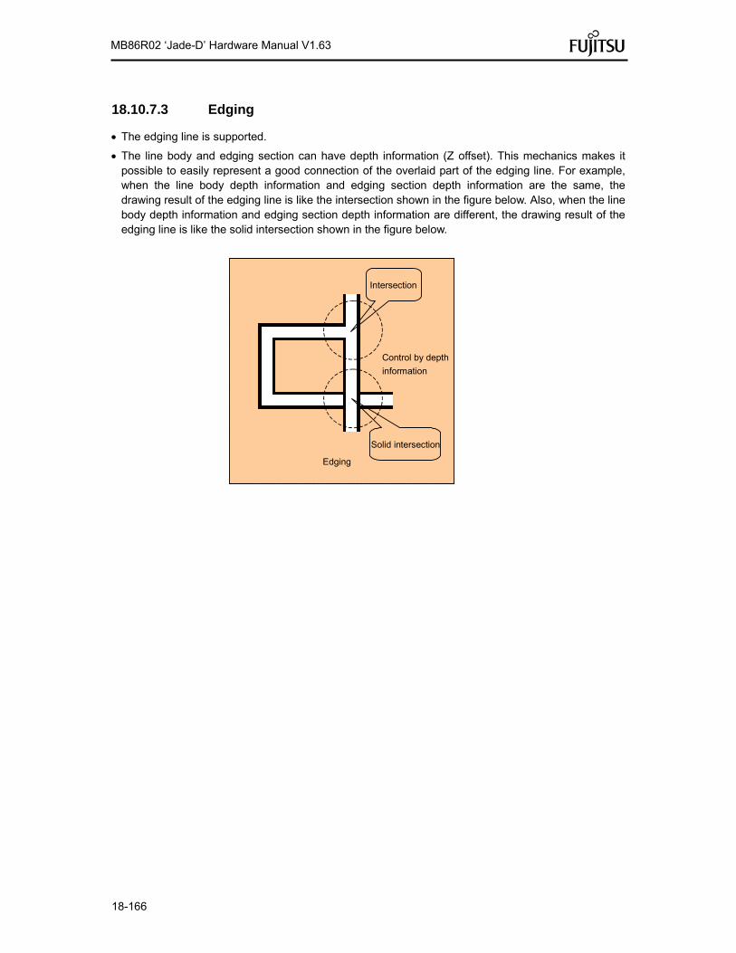
18-166
MB86R02 ‘Jade-D’ Hardware Manual V1.63
18.10.7.3 Edging
The edging line is supported.
The line body and edging section can have depth information (Z offset). This mechanics makes it possible to easily represent a good connection of the overlaid part of the edging line. For example, when the line body depth information and edging section depth information are the same, the drawing result of the edging line is like the intersection shown in the figure below. Also, when the line body depth information and edging section depth information are different, the drawing result of the edging line is like the solid intersection shown in the figure below.
Edging
Intersection
Solid intersection
Control by depth
information

18-167
MB86R02 ‘Jade-D’ Hardware Manual V1.63
18.10.7.4 Interpolation of bold line joint
In the bold line joint interpolation mode, the bold line joint is interpolated using a triangle as shown in the figure below.
The edging line joint is also interpolated using a triangle, but the said depth information makes it possible to represent a good connection as shown in the figure below.
Only LineStrip primitive can interpolate and clipping sometimes breaks LineStrip.
Caution: Sometime joint shape looks not perfect. (using approximate calculation)
Interpolation of bold line joint
Interpolation using
triangle
Edging interpolation can
also be performed.

18-168
MB86R02 ‘Jade-D’ Hardware Manual V1.63
18.10.8 Shadowing
18.10.8.1 Shadowing
The MB86R02 'Jade-D' supports a shadow primitive which is same shape as a body. A shadow is drawn in a position shifted for a device coordinate(X, Y) by setting the OverlapXY command. And by setting the OverlapZ, it is possible to control a drawing result to avoid twice rendering in alpha blend or logical calculation.
- Line
Two shadow lines are drawn in a line shadowing. One is a shadow line and another is a shadow composition line. A shadow composition line is used for avoiding an overlap with body line. And drawing priority can be set for rendering performance or anti-aliasing.
- Triangle and polygon A shadow primitive are drawn in a triangle and polygon shadowing. Drawing priority is fixed as a body primitive is first.
Body line
Shadow line
Shadow composition line
Body primitive
Shadow primitive
18.11 Display Lists
18.11.1 Overview
Display list is a set of display list commands, parameters and pattern data. All display list commands stored in a display list are executed consequently.
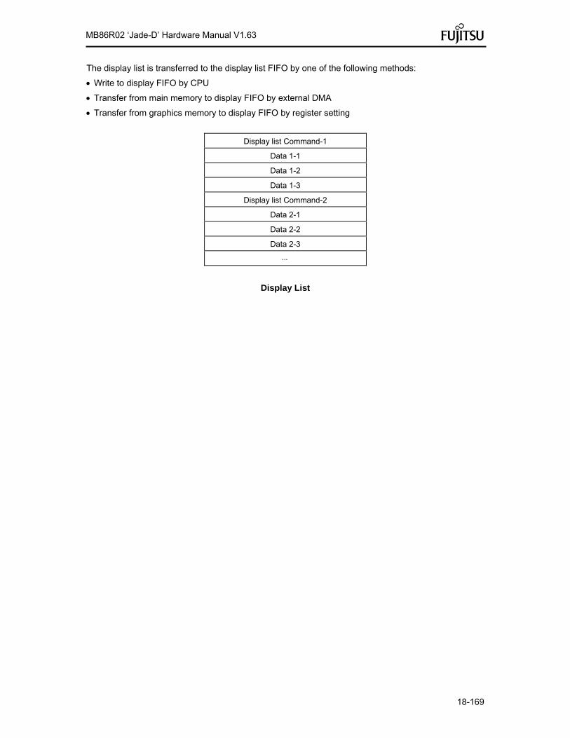
18-169
MB86R02 ‘Jade-D’ Hardware Manual V1.63
The display list is transferred to the display list FIFO by one of the following methods:
Write to display FIFO by CPU
Transfer from main memory to display FIFO by external DMA
Transfer from graphics memory to display FIFO by register setting
Display list Command-1
Data 1-1
Data 1-2
Data 1-3
Display list Command-2
Data 2-1
Data 2-2
Data 2-3
Display List
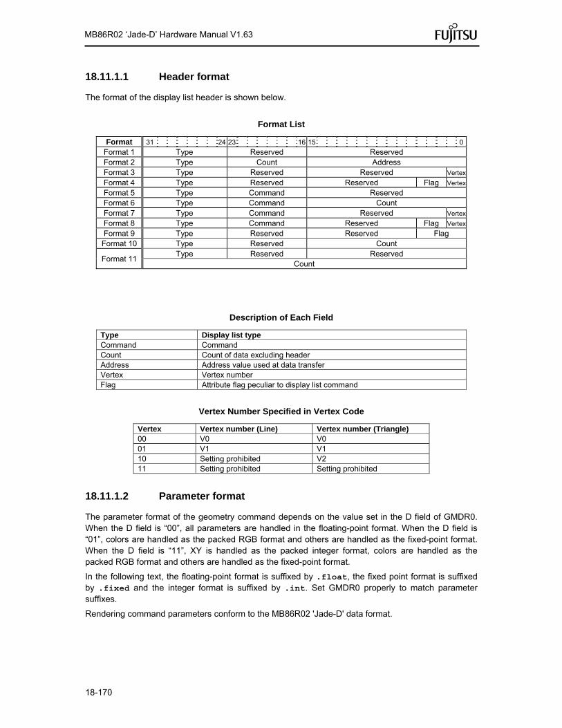
18-170
MB86R02 ‘Jade-D’ Hardware Manual V1.63
18.11.1.1 Header format
The format of the display list header is shown below.
Format List
Format 31 24 23 16 15 0
Format 1 Type Reserved Reserved Format 2 Type Count Address Format 3 Type Reserved Reserved Vertex
Format 4 Type Reserved Reserved Flag Vertex
Format 5 Type Command Reserved Format 6 Type Command Count Format 7 Type Command Reserved Vertex
Format 8 Type Command Reserved Flag Vertex
Format 9 Type Reserved Reserved Flag Format 10 Type Reserved Count
Format 11 Type Reserved Reserved
Count
Description of Each Field
Type Display list type Command Command Count Count of data excluding header Address Address value used at data transfer Vertex Vertex number Flag Attribute flag peculiar to display list command
Vertex Number Specified in Vertex Code
Vertex Vertex number (Line) Vertex number (Triangle) 00 V0 V0 01 V1 V1 10 Setting prohibited V2 11 Setting prohibited Setting prohibited
18.11.1.2 Parameter format
The parameter format of the geometry command depends on the value set in the D field of GMDR0. When the D field is “00”, all parameters are handled in the floating-point format. When the D field is “01”, colors are handled as the packed RGB format and others are handled as the fixed-point format. When the D field is “11”, XY is handled as the packed integer format, colors are handled as the packed RGB format and others are handled as the fixed-point format.
In the following text, the floating-point format is suffixed by .float, the fixed point format is suffixed by .fixed and the integer format is suffixed by .int. Set GMDR0 properly to match parameter suffixes.
Rendering command parameters conform to the MB86R02 'Jade-D' data format.

18-171
MB86R02 ‘Jade-D’ Hardware Manual V1.63
18.11.2 Geometry Commands
18.11.2.1 Geometry command list
MB86R02 'Jade-D' geometry commands and each command code are shown in the table below. Type Command Description
G_Nop No operation
G_Begin See Geometry command code table (1)(2).
Specifies primitive type and pre-processes
G_BeginE See Geometry command code table (3)(4).
Specifies primitive type and pre-processes
This command is used at execution of the MB86R02 'Jade-D' extended function.
G_End Ends primitive
This command is used at execution of G_Begin
G_EndE Ends primitive
This command is used at execution of G_BeginE
G_Vertex Sets vertex parameter and draws
G_VertexLOG Sets vertex parameter and draws
Outputs device coordinates
G_VertexNopLOG Only outputs device coordinates
G_Init Initialize geometry engine
G_Viewport Scale to screen coordinates (X, Y) and set origin offset
G_DepthRange Scale to screen coordinates (Z) and set origin offset
G_LoadMatirix Load geometric transformation matrix
G_ViewVolumeXYClip Set boundary value (X, Y) of view volume clip
G_ViewVolumeZClip Set boundary value (Z) of view volume clip
G_ViewVolumeWClip Set boundary value (W) of view volume clip
OverlapXYOfft See Command table. Sets XY offset at shading
OverlapZOfft See Command table. Sets Z offset of shade primitive; sets Z offset of edge primitive; sets Z offset of interpolation primitive at 2D drawing with top-left non-applicable
DC_LogOutAddr Sets starting address of device coordinates output
SetModeRegister See Command table. Sets drawing extended mode register
SetGModeRegister See Command table. Sets geometry extended mode register
SetColorRegister See Command table. Sets body color, shade color and edge color
SetLVertex2i Pass through high-speed 2DLine drawing register
SetLVertex2iP Pass through high-speed 2DLine drawing register

18-172
MB86R02 ‘Jade-D’ Hardware Manual V1.63
Type code table
Type Code
G_Nop 0010_0000 G_Begin 0010_0001 G_End 0010_0011 G_Vertex 0011_0000 G_VertexLOG 0011_0010 G_VertexNopLOG 0011_0011 G_Init 0100_0000 G_Viewport 0100_0001 G_DepthRange 0100_0010 G_LoadMatirix 0100_0011 G_ViewVolumeXYClip 0100_0100 G_ViewVolumeZClip 0100_0101 G_ViewVolumeWClip 0100_0110 SetLVertex2i 0111_0010 SetLVertex2iP 0111_0011 SetModeRegister 1100_0000 SetGModeRegister 1100_0001 OverlapXY0fft 1100_1000 OverlapZ0fft 1100_1001 DC_LogOutAddr 1100_1100 SetColorRegister 1100_1110 G_BeginE 1110_0001 G_EndE 1110_0011
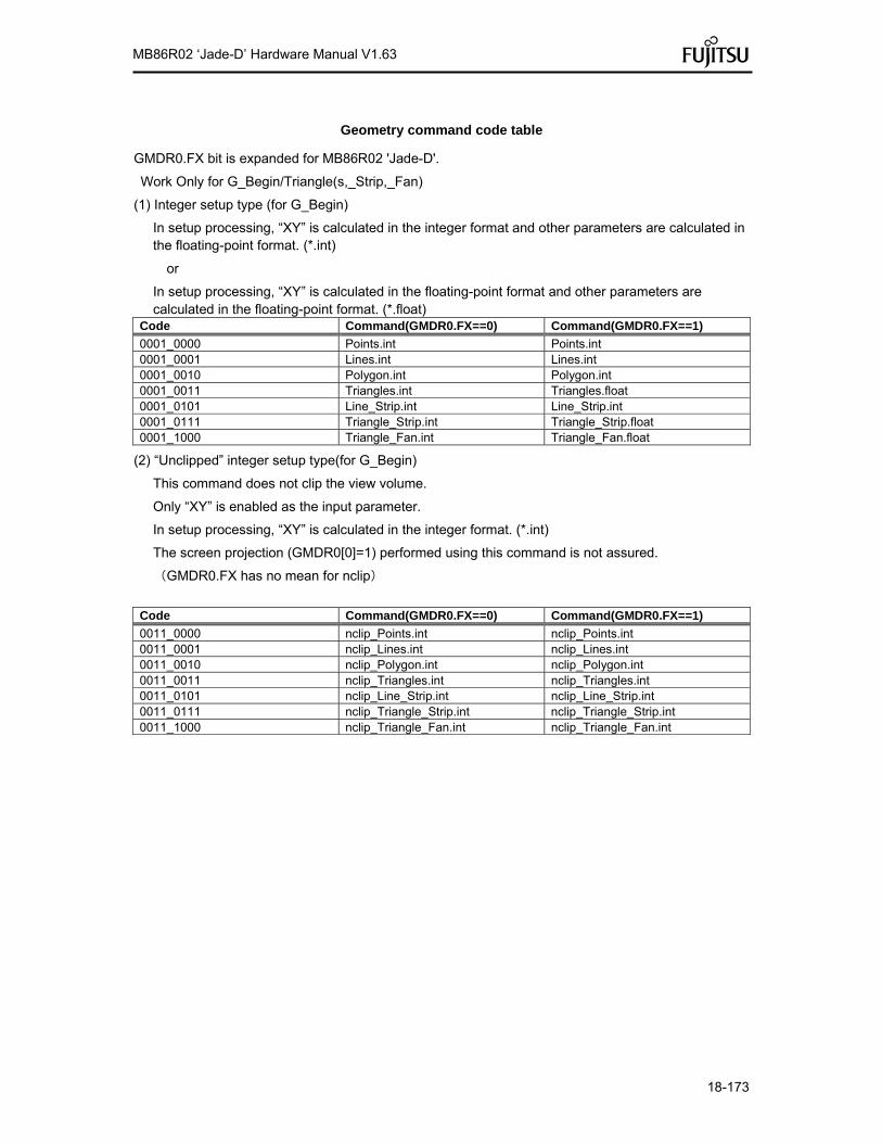
18-173
MB86R02 ‘Jade-D’ Hardware Manual V1.63
Geometry command code table
GMDR0.FX bit is expanded for MB86R02 'Jade-D'.
Work Only for G_Begin/Triangle(s,_Strip,_Fan)
(1) Integer setup type (for G_Begin)
In setup processing, “XY” is calculated in the integer format and other parameters are calculated in the floating-point format. (*.int)
or
In setup processing, “XY” is calculated in the floating-point format and other parameters are calculated in the floating-point format. (*.float)
Code Command(GMDR0.FX==0) Command(GMDR0.FX==1)
0001_0000 Points.int Points.int 0001_0001 Lines.int Lines.int 0001_0010 Polygon.int Polygon.int 0001_0011 Triangles.int Triangles.float 0001_0101 Line_Strip.int Line_Strip.int 0001_0111 Triangle_Strip.int Triangle_Strip.float 0001_1000 Triangle_Fan.int Triangle_Fan.float
(2) “Unclipped” integer setup type(for G_Begin)
This command does not clip the view volume.
Only “XY” is enabled as the input parameter.
In setup processing, “XY” is calculated in the integer format. (*.int)
The screen projection (GMDR0[0]=1) performed using this command is not assured.
(GMDR0.FX has no mean for nclip)
Code Command(GMDR0.FX==0) Command(GMDR0.FX==1)
0011_0000 nclip_Points.int nclip_Points.int 0011_0001 nclip_Lines.int nclip_Lines.int 0011_0010 nclip_Polygon.int nclip_Polygon.int 0011_0011 nclip_Triangles.int nclip_Triangles.int 0011_0101 nclip_Line_Strip.int nclip_Line_Strip.int 0011_0111 nclip_Triangle_Strip.int nclip_Triangle_Strip.int 0011_1000 nclip_Triangle_Fan.int nclip_Triangle_Fan.int
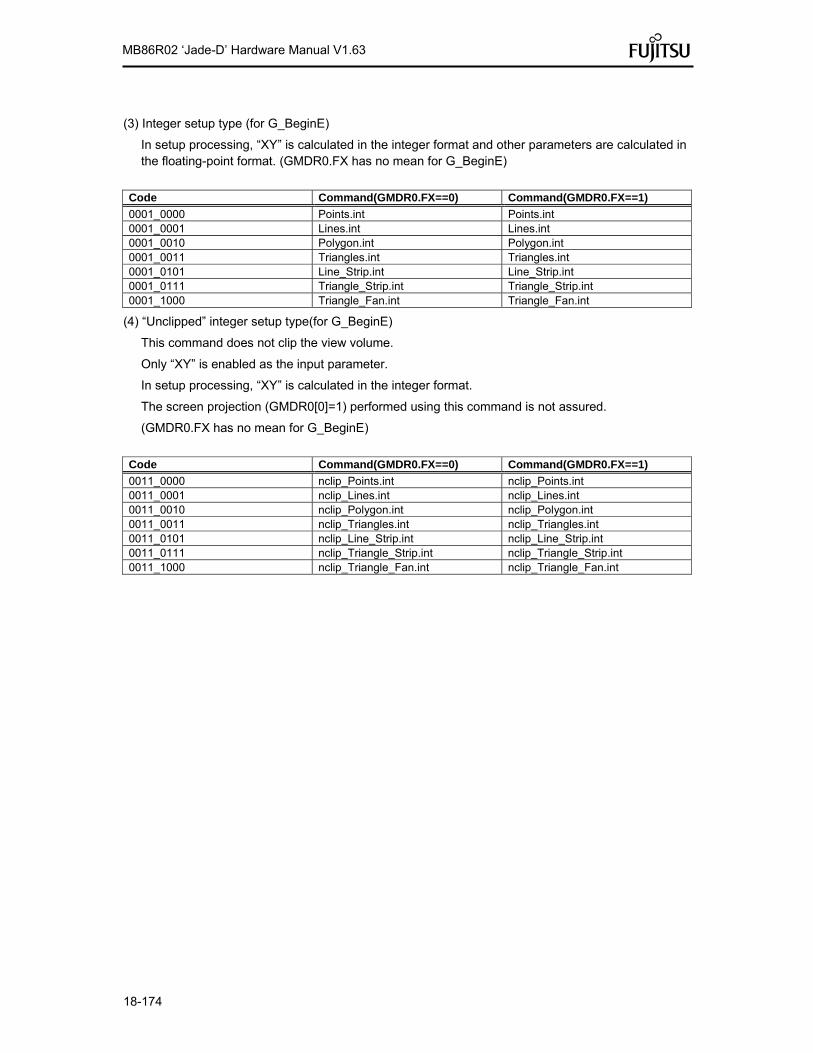
18-174
MB86R02 ‘Jade-D’ Hardware Manual V1.63
(3) Integer setup type (for G_BeginE)
In setup processing, “XY” is calculated in the integer format and other parameters are calculated in the floating-point format. (GMDR0.FX has no mean for G_BeginE)
Code Command(GMDR0.FX==0) Command(GMDR0.FX==1)
0001_0000 Points.int Points.int 0001_0001 Lines.int Lines.int 0001_0010 Polygon.int Polygon.int 0001_0011 Triangles.int Triangles.int 0001_0101 Line_Strip.int Line_Strip.int 0001_0111 Triangle_Strip.int Triangle_Strip.int 0001_1000 Triangle_Fan.int Triangle_Fan.int
(4) “Unclipped” integer setup type(for G_BeginE)
This command does not clip the view volume.
Only “XY” is enabled as the input parameter.
In setup processing, “XY” is calculated in the integer format.
The screen projection (GMDR0[0]=1) performed using this command is not assured.
(GMDR0.FX has no mean for G_BeginE)
Code Command(GMDR0.FX==0) Command(GMDR0.FX==1)
0011_0000 nclip_Points.int nclip_Points.int 0011_0001 nclip_Lines.int nclip_Lines.int 0011_0010 nclip_Polygon.int nclip_Polygon.int 0011_0011 nclip_Triangles.int nclip_Triangles.int 0011_0101 nclip_Line_Strip.int nclip_Line_Strip.int 0011_0111 nclip_Triangle_Strip.int nclip_Triangle_Strip.int 0011_1000 nclip_Triangle_Fan.int nclip_Triangle_Fan.int

18-175
MB86R02 ‘Jade-D’ Hardware Manual V1.63
18.11.2.2 Explanation of geometry commands
G_Nop (Format 1) 31 24 23 16 15 0
G_Nop Reserved Reserved
No operation
G_Init (Format 1) 31 24 23 16 15 0
G_Init Reserved Reserved
The GInit command initializes geometry engine. Execute this command before processing.
G_End (Format 1) 31 24 23 16 15 0
G_End Reserved Reserved
The G_End command ends one primitive. The G_Vertex command must be specified between the G_Begin command and G_End command.

18-176
MB86R02 ‘Jade-D’ Hardware Manual V1.63
G_Begin (Format 5) 31 24 23 16 15 0
G_Begin Command Reserved
The G_Begin command sets types of primitive for geometry processing and drawing. A vertex is set and drawn by the G_Vertex command. The G_Vertex command must be specified between the G_Begin command and G_End command.
Only G_Vertex or SetRegister for FC/BC (XY Only vertex) can placed between G_Begin and G_End.
Command:
Points* Handles primitive as point
Lines* Handles primitive as independent line
Polygon* Handles primitive as polygon
Triangles* Handles primitive as independent triangle
Line_Strip* Handles primitive as line strip
Triangle_Strip* Handles primitive as triangle strip
Triangle_Fan* Handles primitive as triangle fan
Usable combinations of GMDR0 mode setting and primitives are as follows:
Unclipped primitives (nclip*)
(ST,Z,C) Point Line Triangle Polygon
(0,0,0)
Other than above
Primitives other than unclipped primitives
(ST,Z,C) Point Line Triangle Polygon
(0,0,0)
(0,0,1)
(0,1,0)
(0,1,1)
(1,x,x)
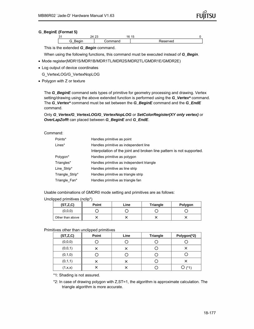
18-177
MB86R02 ‘Jade-D’ Hardware Manual V1.63
G_BeginE (Format 5) 31 24 23 16 15 0
G_Begin Command Reserved
This is the extended G_Begin command.
When using the following functions, this command must be executed instead of G_Begin.
Mode register(MDR1S/MDR1B/MDR1TL/MDR2S/MDR2TL/GMDR1E/GMDR2E)
Log output of device coordinates
G_VertexLOG/G_VertexNopLOG
Polygon with Z or texture
The G_BeginE command sets types of primitive for geometry processing and drawing. Vertex setting/drawing using the above extended function is performed using the G_Vertex* command. The G_Vertex* command must be set between the G_BeginE command and the G_EndE command.
Only G_Vertex/G_VertexLOG/G_VertexNopLOG or SetColorRegister(XY only vertex) or OverLapZofft can placed between G_BeginE and G_EndE.
Command:
Points* Handles primitive as point
Lines* Handles primitive as independent line
Interpolation of the joint and broken line pattern is not supported.
Polygon* Handles primitive as polygon
Triangles* Handles primitive as independent triangle
Line_Strip* Handles primitive as line strip
Triangle_Strip* Handles primitive as triangle strip
Triangle_Fan* Handles primitive as triangle fan
Usable combinations of GMDR0 mode setting and primitives are as follows:
Unclipped primitives (nclip*)
(ST,Z,C) Point Line Triangle Polygon
(0,0,0)
Other than above
Primitives other than unclipped primitives
(ST,Z,C) Point Line Triangle Polygon(*2)
(0,0,0)
(0,0,1)
(0,1,0)
(0,1,1)
(1,x,x) (*1)
*1: Shading is not assured.
*2: In case of drawing polygon with Z,ST=1, the algorithm is approximate calculation. The triangle algorithm is more accurate.
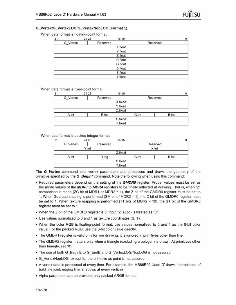
18-178
MB86R02 ‘Jade-D’ Hardware Manual V1.63
G_Vertex/G_VertexLOG/G_VertexNopLOG (Format 1)
When data format is floating-point format 31 24 23 16 15 0
G_Vertex Reserved Reserved X.float Y.float Z.float R.float G.float B.float S.float T.float
When data format is fixed-point format 31 24 23 16 15 0
G_Vertex Reserved Reserved X.fixed Y.fixed Z.fixed
A.int R.int G.int B.int S.fixed T.fixed
When data format is packed integer format 31 24 23 16 15 0
G_Vertex Reserved Reserved Y.int X.int
Z.fixed A.int R.ing G.int B.int
S.fixed T.fixed
The G_Vertex command sets vertex parameters and processes and draws the geometry of the primitive specified by the G_Begin* command. Note the following when using this command:
Required parameters depend on the setting of the GMDR0 register. Proper values must be set as the mode values of the MDR0 to MDR4 registers to be finally reflected at drawing. That is, when “Z” comparison is made (ZC bit of MDR1 or MDR2 = 1), the Z bit of the GMDR0 register must be set to 1. When Gouraud shading is performed (SM bit of MDR2 = 1), the C bit of the GMDR0 register must be set to 1. When texture mapping is performed (TT bits of MDR2 = 10), the ST bit of the GMDR0 register must be set to 1.
When the Z bit of the GMDR0 register is 0, input “Z” (Zoc) is treated as “0”.
Use values normalized to 0 and 1 as texture coordinates (S, T).
When the color RGB is floating-point format, use values normalized to 0 and 1 as the 8-bit color value. For the packed RGB, use the 8-bit color value directly.
The GMDR1 register is valid only for line drawing; it is ignored in primitives other than line.
The GMDR2 register matters only when a triangle (excluding a polygon) is drawn. At primitives other than triangle, set “0”.
The use of both G_BeginE to G_EndE and G_VertexLOG/NopLOG is not assured.
G_VertexNopLOG, except for the primitive as point is not assured.
A vertex data is processed at every time. For example, the MB86R02 'Jade-D' draws interpolation of bold line joint, edging line, shadows at every vertices.
Alpha parameter can be provided only packed ARGB format.
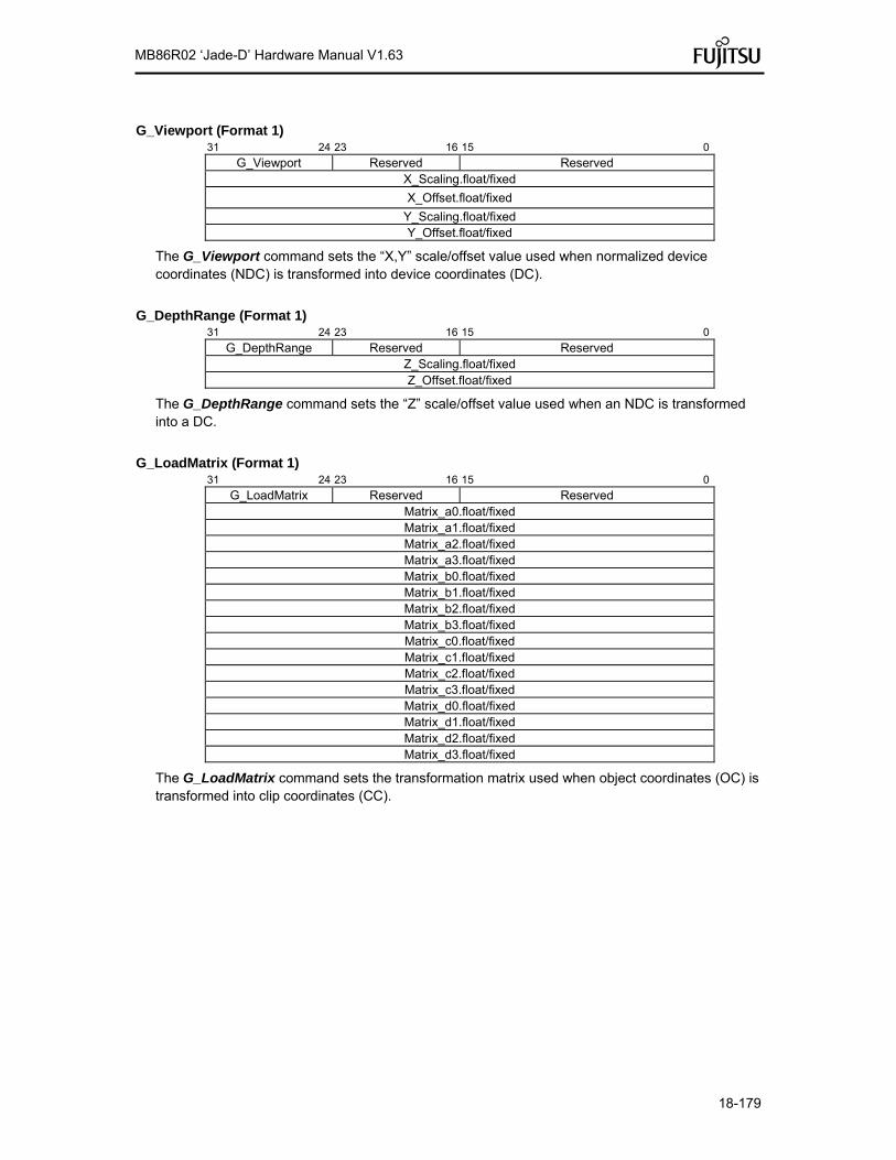
18-179
MB86R02 ‘Jade-D’ Hardware Manual V1.63
G_Viewport (Format 1) 31 24 23 16 15 0
G_Viewport Reserved Reserved X_Scaling.float/fixed
X_Offset.float/fixed
Y_Scaling.float/fixed Y_Offset.float/fixed
The G_Viewport command sets the “X,Y” scale/offset value used when normalized device coordinates (NDC) is transformed into device coordinates (DC).
G_DepthRange (Format 1) 31 24 23 16 15 0
G_DepthRange Reserved Reserved Z_Scaling.float/fixed Z_Offset.float/fixed
The G_DepthRange command sets the “Z” scale/offset value used when an NDC is transformed into a DC.
G_LoadMatrix (Format 1) 31 24 23 16 15 0
G_LoadMatrix Reserved Reserved Matrix_a0.float/fixed Matrix_a1.float/fixed Matrix_a2.float/fixed Matrix_a3.float/fixed Matrix_b0.float/fixed Matrix_b1.float/fixed Matrix_b2.float/fixed Matrix_b3.float/fixed Matrix_c0.float/fixed Matrix_c1.float/fixed Matrix_c2.float/fixed Matrix_c3.float/fixed Matrix_d0.float/fixed Matrix_d1.float/fixed Matrix_d2.float/fixed Matrix_d3.float/fixed
The G_LoadMatrix command sets the transformation matrix used when object coordinates (OC) is transformed into clip coordinates (CC).

18-180
MB86R02 ‘Jade-D’ Hardware Manual V1.63
G_ViewVolumeXYClip (Format 1) 31 24 23 16 15 0
G_ViewVolumeXYClip Reserved Reserved XMIN.float/fixed XMAX.float/fixed YMIN.float/fixed YMAX.float/fixed
The G_ViewVolumeXYClip command sets the X,Y coordinates of the clip boundary value in view volume clipping.
G_ViewVolumeZClip (Format 1) 31 24 23 16 15 0
G_ViewVolumeZClip Reserved Reserved ZMIN.float/fixed ZMAX.float/fixed
The G_ViewVolumeZClip command sets the Z coordinates of the clip boundary value in view volume clipping.
G_ViewVolumeWClip (Format 1) 31 24 23 16 15 0
G_ViewVolumeWClip Reserved Reserved WMIN.float/fixed
The G_ViewVolumeWClip command sets the W coordinates of the clip boundary value in view volume clipping (minimum value only).

18-181
MB86R02 ‘Jade-D’ Hardware Manual V1.63
OverlapXYOfft (Format5) 31 24 23 16 15 0
OverlapXYOfft Command Reserved
Y Offset X Offset
The OverlapXYOfft command sets the XY offset of the shade primitive relative to the body primitive at shading drawing. Shadow shape is same as body.
Command:
Command Code Explanation
ShadowXY 0000_0000 ShadowXY command sets the XY offset of the shade primitive relative to the body primitive.
ShadowXYcompsition 0000_0001 ShadowXYcomposition command sets the XY offset of the shade synthetic primitive relative to the body primitive. It command synthesizes a shade from the relationship between the XY offset set using ShadowXY and this XY offset. This command is enabled for only lines.
OverlapZOfft (Format5) 31 24 23 16 15 0
OverlapZOfft Command Reserved
don’t care Z Offset
Note: When MDR0 ZP = 1, only lower 8 bits are enabled.
31 24 23 16 15 0
OverlapZOfft Packed_ONBS Reserved
SZ Offset BZ Offset NZ Offset OZ Offset
The OverlapZOfft command sets the Z offset of the shade primitive relative to the body primitive, sets the Z-offset of the edge primitive relative to the body primitive and sets the Z offset of the interpolation primitive relative to the body primitive, with the top-left rule non-applicable in effect.
At this time, the following relationship must be satisfied when, for example, GREATER is specified for the Z value comparison mode:
Body primitive > Top-left rule non-applicable interpolation primitive > Edge primitive > Shade primitive
Command:
Command Code Explanation
Origin 0000_0000 Origin command sets the Z offset of the body primitive. When drawing one primitive below the other primitive (for example, when drawing a solid intersection), this Z offset is changed. When drawing an ordinary intersection, set the same Z offset as other primitives.
NonTopLeft 0000_0001 NonTopLeft command sets the Z offset of the interpolation primitive, with the top-left non-applicable.
Border 0000_0010 Border command sets the Z offset of the edge primitive.
Shadow 0000_0011 Shadow command sets the Z offset of the shade primitive.
Packed_ONBS 0000_0111 Packed_ONBS command sets the above four types of Z offsets.
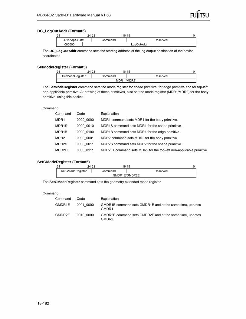
18-182
MB86R02 ‘Jade-D’ Hardware Manual V1.63
DC_LogOutAddr (Format5) 31 24 23 16 15 0
OverlapXYOfft Command Reserved
000000 LogOutAddr
The DC_LogOutAddr command sets the starting address of the log output destination of the device
coordinates.
SetModeRegister (Format5) 31 24 23 16 15 0
SetModeRegister Command Reserved
MDR1*/MDR2*
The SetModeRegister command sets the mode register for shade primitive, for edge primitive and for top-left
non-applicable primitive. At drawing of these primitives, also set the mode register (MDR1/MDR2) for the body
primitive, using this packet.
Command:
Command Code Explanation
MDR1 0000_0000 MDR1 command sets MDR1 for the body primitive.
MDR1S 0000_0010 MDR1S command sets MDR1 for the shade primitive.
MDR1B 0000_0100 MDR1B command sets MDR1 for the edge primitive.
MDR2 0000_0001 MDR2 command sets MDR2 for the body primitive.
MDR2S 0000_0011 MDR2S command sets MDR2 for the shade primitive.
MDR2LT 0000_0111 MDR2LT command sets MDR2 for the top-left non-applicable primitive.
SetGModeRegister (Format5) 31 24 23 16 15 0
SetGModeRegister Command Reserved
GMDR1E/GMDR2E
The SetGModeRegister command sets the geometry extended mode register.
Command:
Command Code Explanation
GMDR1E 0001_0000 GMDR1E command sets GMDR1E and at the same time, updates GMDR1.
GMDR2E 0010_0000 GMDR2E command sets GMDR2E and at the same time, updates GMDR2.

18-183
MB86R02 ‘Jade-D’ Hardware Manual V1.63
SetColorRegister (Format5) 31 24 23 16 15 0
SetColorRegister Command Reserved
FGC8/16/24
The SetColorRegister command sets the foreground color and background color of the body primitive, shade
primitive and edge primitive.
Commands:
Command Code Explanation
ForeColor 0000_0000 ForeColor command sets the foreground color for the body primitive.
BackColor 0000_0001 BackColor command sets the background color for the body primitive.
ForeColorShadow 0000_0010 ForeColorShadow command sets the foreground color for the shade primitive.
BackColorShadow 0000_0011 BackColorShadow command sets the background color for the shade primitive.
ForeColorBorder 0000_0100 ForeColorBorder command sets the foreground color for the edge primitive.
BackColorBorder 0000_0101 BackColorBorder command sets the background color for the edge primitive.
SetRegister (Format 2) 31 24 23 16 15 0
SetRegister Count Address
(Val 0)
(Val 1)
…
(Val n)
The SetRegister command is upper compatible with CREMSON SetRegister. It can specify the address of a
register in the geometry engine.
SetLVertex2i (Format 1) 31 24 23 16 15 0
SetLVertex2i Reserved Reserved
LX0dc
LY0dc
The SetLVertex2i command issues the SetRegister_LXOdc/LYOdc command (MB86290A command to set
starting vertex at line drawing) in the geometry FIFO interface. This performs processing faster than when the
SetRegister_LXOdc/LYOdc command is input directly to the geometry FIFO.
SetLVertex2iP (Format 1) 31 24 23 16 15 0
SetLVertex2iP Reserved Reserved
LY0dc LX0dc
The SetLVertex2iP command supports packed XY of SetLVertex2i.
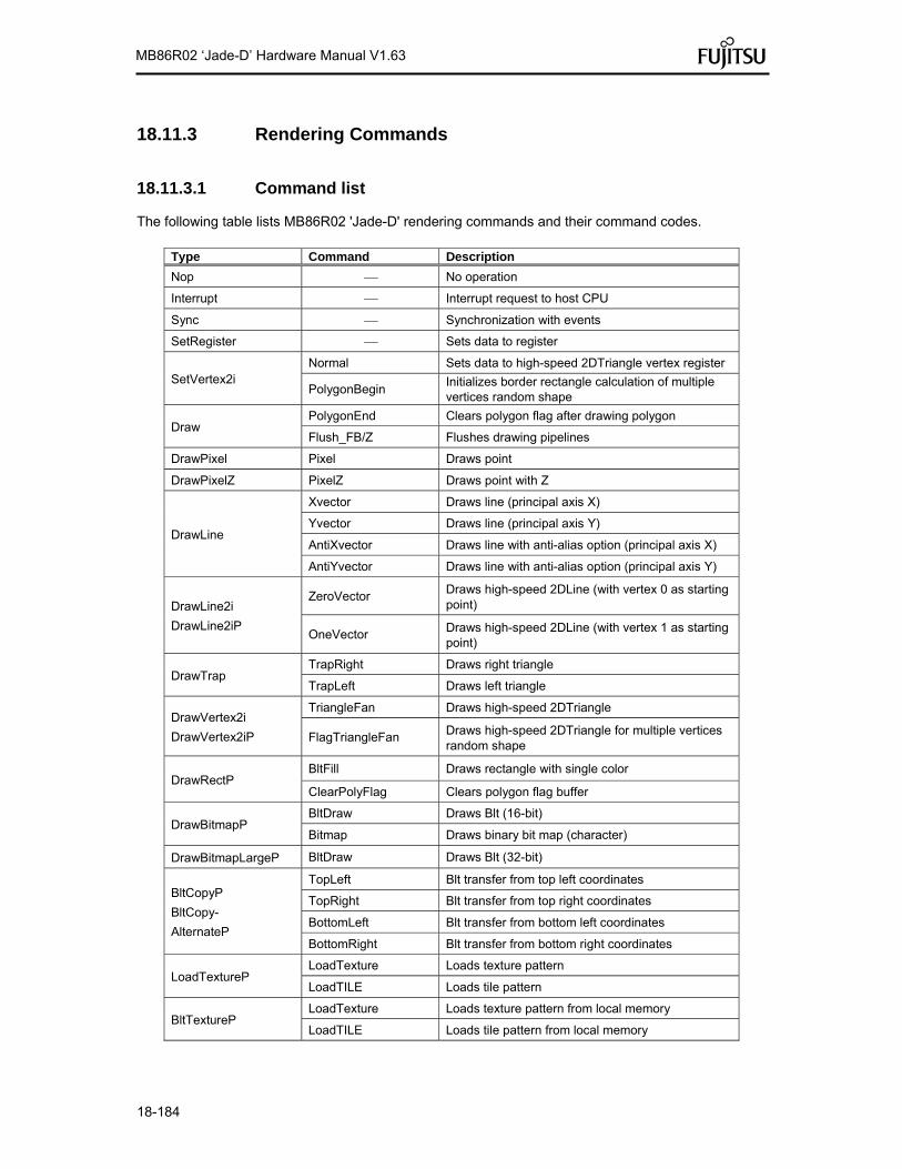
18-184
MB86R02 ‘Jade-D’ Hardware Manual V1.63
18.11.3 Rendering Commands
18.11.3.1 Command list
The following table lists MB86R02 'Jade-D' rendering commands and their command codes.
Type Command Description
Nop No operation
Interrupt Interrupt request to host CPU
Sync Synchronization with events
SetRegister Sets data to register
SetVertex2i Normal Sets data to high-speed 2DTriangle vertex register
PolygonBegin Initializes border rectangle calculation of multiple vertices random shape
Draw PolygonEnd Clears polygon flag after drawing polygon
Flush_FB/Z Flushes drawing pipelines
DrawPixel Pixel Draws point
DrawPixelZ PixelZ Draws point with Z
DrawLine
Xvector Draws line (principal axis X)
Yvector Draws line (principal axis Y)
AntiXvector Draws line with anti-alias option (principal axis X)
AntiYvector Draws line with anti-alias option (principal axis Y)
DrawLine2i
DrawLine2iP
ZeroVector Draws high-speed 2DLine (with vertex 0 as starting point)
OneVector Draws high-speed 2DLine (with vertex 1 as starting point)
DrawTrap TrapRight Draws right triangle
TrapLeft Draws left triangle
DrawVertex2i
DrawVertex2iP
TriangleFan Draws high-speed 2DTriangle
FlagTriangleFan Draws high-speed 2DTriangle for multiple vertices random shape
DrawRectP BltFill Draws rectangle with single color
ClearPolyFlag Clears polygon flag buffer
DrawBitmapP BltDraw Draws Blt (16-bit)
Bitmap Draws binary bit map (character)
DrawBitmapLargeP BltDraw Draws Blt (32-bit)
BltCopyP
BltCopy-
AlternateP
TopLeft Blt transfer from top left coordinates
TopRight Blt transfer from top right coordinates
BottomLeft Blt transfer from bottom left coordinates
BottomRight Blt transfer from bottom right coordinates
LoadTextureP LoadTexture Loads texture pattern
LoadTILE Loads tile pattern
BltTextureP LoadTexture Loads texture pattern from local memory
LoadTILE Loads tile pattern from local memory

18-185
MB86R02 ‘Jade-D’ Hardware Manual V1.63
BltCopyAlt-
AlphaBlendP
Alpha blending is supported (see the alpha map). BltCopyAlternateP
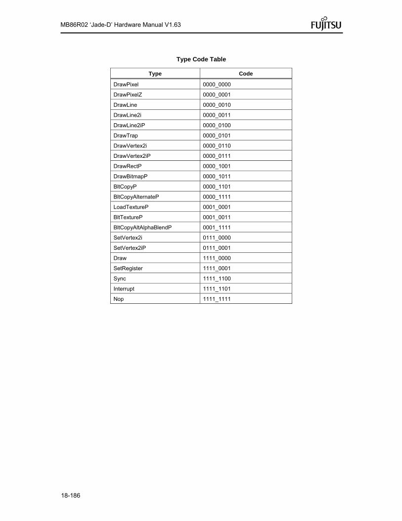
18-186
MB86R02 ‘Jade-D’ Hardware Manual V1.63
Type Code Table
Type Code
DrawPixel 0000_0000
DrawPixelZ 0000_0001
DrawLine 0000_0010
DrawLine2i 0000_0011
DrawLine2iP 0000_0100
DrawTrap 0000_0101
DrawVertex2i 0000_0110
DrawVertex2iP 0000_0111
DrawRectP 0000_1001
DrawBitmapP 0000_1011
BltCopyP 0000_1101
BltCopyAlternateP 0000_1111
LoadTextureP 0001_0001
BltTextureP 0001_0011
BltCopyAltAlphaBlendP 0001_1111
SetVertex2i 0111_0000
SetVertex2iP 0111_0001
Draw 1111_0000
SetRegister 1111_0001
Sync 1111_1100
Interrupt 1111_1101
Nop 1111_1111

18-187
MB86R02 ‘Jade-D’ Hardware Manual V1.63
Command Code Table (1)
Command Code
Pixel 000_00000
PixelZ 000_00001
Xvector 001_00000
Yvector 001_00001
XvectorNoEnd 001_00010
YvectorNoEnd 001_00011
XvectorBlpClear 001_00100
YvectorBlpClear 001_00101
XvectorNoEndBlpClear 001_00110
YvectorNoEndBlpClear 001_00111
AntiXvector 001_01000
AntiYvector 001_01001
AntiXvectorNoEnd 001_01010
AntiYvectorNoEnd 001_01011
AntiXvectorBlpClear 001_01100
AntiYvectorBlpClear 001_01101
AntiXvectorNoEndBlpClear 001_01110
AntiYvectorNoEndBlpClear 001_01111
ZeroVector 001_10000
Onevector 001_10001
ZeroVectorNoEnd 001_10010
OnevectorNoEnd 001_10011
ZeroVectorBlpClear 001_10100
OnevectorBlpClear 001_10101
ZeroVectorNoEndBlpClear 001_10110
OnevectorNoEndBlpClear 001_10111
AntiZeroVector 001_11000
AntiOnevector 001_11001
AntiZeroVectorNoEnd 001_11010
AntiOnevectorNoEnd 001_11011
AntiZeroVectorBlpClear 001_11100
AntiOnevectorBlpClear 001_11101
AntiZeroVectorNoEndBlpClear 001_11110
AntiOnevectorNoEndBlpClear 001_11111

18-188
MB86R02 ‘Jade-D’ Hardware Manual V1.63
Command Code Table (2)
Command Code
BltFill 010_00001
BltDraw 010_00010
Bitmap 010_00011
TopLeft 010_00100
TopRight 010_00101
BottomLeft 010_00110
BottomRight 010_00111
LoadTexture 010_01000
LoadTILE 010_01001
TrapRight 011_00000
TrapLeft 011_00001
TriangleFan 011_00010
FlagTriangleFan 011_00011
Flush_FB 110_00001
Flush_Z 110_00010
PolygonBegin 111_00000
PolygonEnd 111_00001
ClearPolyFlag 111_00010
Normal 111_11111

18-189
MB86R02 ‘Jade-D’ Hardware Manual V1.63
18.11.3.2 Details of rendering commands
All parameters belonging to their command are stored in relevant registers. The definition of each parameter is explained in the section of each command.
Nop (Format1) 31 24 23 16 15 0
Nop Reserved Reserved
No operation
Interrupt (Format1) 31 24 23 16 15 0
Interrupt Reserved Reserved
The Interrupt command generates interrupt request to host CPU.
Sync (Format9) 31 24 23 16 15 4 0
Sleep Reserved Reserved flag
The Sync command suspends all subsequent display list processing until event set in flag detected.
Flag: Bit number 4 3 2 1 0
Bit field name Reserved Reserved Reserved Reserved VBLANK
Bit 0 VBLANK
VBLANK Synchronization
0 No operation
1 Wait for VSYNC detection specified by FS field of MDR0
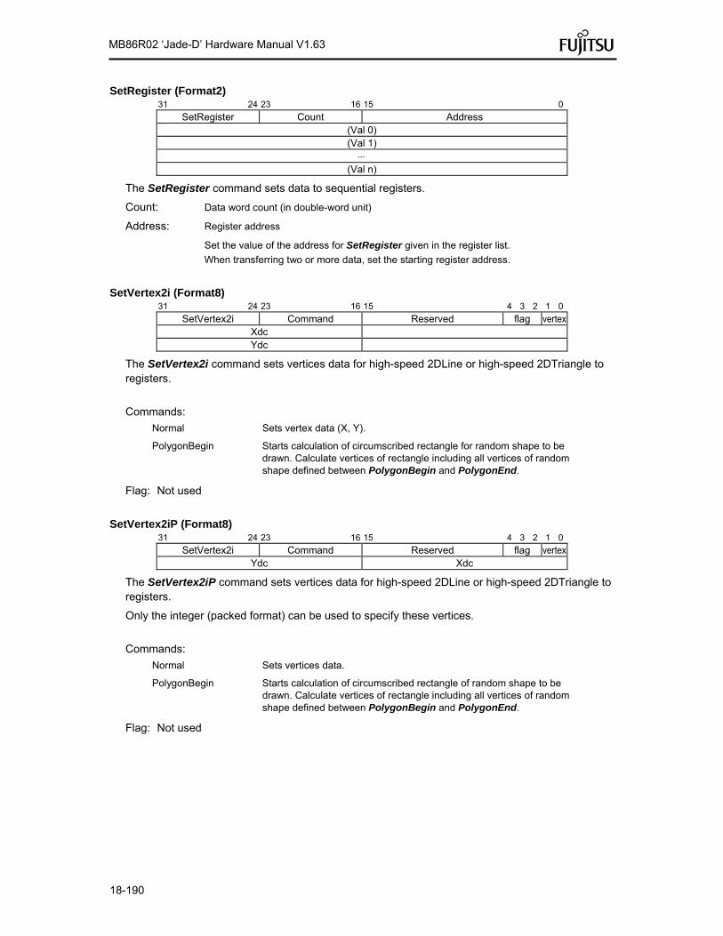
18-190
MB86R02 ‘Jade-D’ Hardware Manual V1.63
SetRegister (Format2) 31 24 23 16 15 0
SetRegister Count Address (Val 0) (Val 1)
(Val n)
The SetRegister command sets data to sequential registers.
Count: Data word count (in double-word unit)
Address: Register address
Set the value of the address for SetRegister given in the register list.
When transferring two or more data, set the starting register address.
SetVertex2i (Format8) 31 24 23 16 15 4 3 2 1 0
SetVertex2i Command Reserved flag vertex Xdc Ydc
The SetVertex2i command sets vertices data for high-speed 2DLine or high-speed 2DTriangle to registers.
Commands:
Normal Sets vertex data (X, Y).
PolygonBegin Starts calculation of circumscribed rectangle for random shape to be drawn. Calculate vertices of rectangle including all vertices of random shape defined between PolygonBegin and PolygonEnd.
Flag: Not used
SetVertex2iP (Format8) 31 24 23 16 15 4 3 2 1 0
SetVertex2i Command Reserved flag vertex Ydc Xdc
The SetVertex2iP command sets vertices data for high-speed 2DLine or high-speed 2DTriangle to registers.
Only the integer (packed format) can be used to specify these vertices.
Commands:
Normal Sets vertices data.
PolygonBegin Starts calculation of circumscribed rectangle of random shape to be drawn. Calculate vertices of rectangle including all vertices of random shape defined between PolygonBegin and PolygonEnd.
Flag: Not used

18-191
MB86R02 ‘Jade-D’ Hardware Manual V1.63
Draw (Format5) 31 24 23 16 15 0
Draw Command Reserved
The Draw command executes drawing command. All parameters required for drawing command execution must be set at their appropriate registers.
Commands:
PolygonEnd Draws polygon end.
Fills random shape with color according to flags generated by FlagTriangleFan command and information of circumscribed rectangle generated by PolygonBegin command.
Flush_FB Flushes drawing data in the drawing pipeline into the graphics memory. Place this command at the end of the display list.
Flush_Z Flushes Z value data in the drawing pipeline into the graphics memory. When using the Z buffer, place this command together with the Flush_FB command at the end of the display list.
DrawPixel (Format5) 31 24 23 16 15 0
DeawPixel Command Reserved PXs PYs
The DrawPixel command draws pixel.
Command:
Pixel Draws pixel without Z value.
DrawPixelZ (Format5) 31 24 23 16 15 0
DeawPixel Command Reserved PXs PYs PZs
The DrawPixelZ command draws pixel with Z value.
Command:
PixelZ Draws pixel with Z value.

18-192
MB86R02 ‘Jade-D’ Hardware Manual V1.63
DrawLine (Format5) 31 24 23 16 15 0
DrawLine Command Reserved LPN LXs
LXde LYs
LYde
The DrawLine command draws line. It starts drawing after setting all parameters at line draw registers.
Commands:
Xvector Draws line (principal axis X).
Yvector Draws line (principal axis Y).
XvectorNoEnd Draws line (principal axis X and without end point drawing).
YvectorNoEnd Draws line (principal axis Y and without end point drawing).
XvectorBlpClear Draws line (principal axis X and prior to drawing, broken line pattern reference position cleared).
YvectorBlpClear Draws line (principal axis Y and prior to drawing, broken line pattern reference position cleared).
XvectorNoEndBlpClear Draws line (principal axis X, without end point drawing and prior to drawing, broken line pattern reference position cleared).
YvectorNoEndBlpClear Draws line (principal axis Y, without end point drawing and prior to drawing, broken line pattern reference position cleared).
AntiXvector Draws anti-alias line (principal axis X).
AntiYvector Draws anti-alias line (principal axis Y).
AntiXvectorNoEnd Draws anti-alias line (principal axis X and without end point drawing).
AntiYvectorNoEnd Draws anti-alias line (principal axis Y and without end point drawing).
AntiXvectorBlpClear Draws anti-alias line (principal axis X and prior to drawing, broken line pattern reference position cleared).
AntiYvectorBlpClear Draws anti-alias line (principal axis Y and prior to drawing, broken line pattern reference position cleared).
AntiXvectorNoEndBlpClear Draws anti-alias line (principal axis X, without end point drawing and prior to drawing, broken line pattern reference position cleared).
AntiYvectorNoEndBlpClear Draws anti-alias line (principal axis Y, without end point drawing and prior to drawing, broken line pattern reference position cleared).

18-193
MB86R02 ‘Jade-D’ Hardware Manual V1.63
DrawLine2i (Format7) 31 24 23 16 15 0
DrawLine2i Command Reserved vertex LFXs 0 LFYs 0
The DrawLine2i command draws high-speed 2DLine. It starts drawing after setting parameters at the high-speed 2DLine drawing registers. Integer data can only be used for coordinates.
Commands:
ZeroVector Draws line from vertex 0 to vertex 1.
OneVector Draws line from vertex 1 to vertex 0.
ZeroVectorNoEnd Draws line from vertex 0 to vertex 1 (without drawing end point).
OneVectorNoEnd Draws line from vertex 1 to vertex 0 (without drawing end point).
ZeroVectorBlpClear Draws line from vertex 0 to vertex 1 (principal axis X and prior to drawing, broken line pattern reference position cleared).
OneVectorBlpClear Draws line from vertex 1 to vertex 0 (principal axis Y and prior to drawing, broken line pattern reference position cleared).
ZeroVectorNoEndBlpClear Draws line from vertex 0 to vertex 1 (principal axis X, without end point drawing and prior to drawing, broken line pattern reference position cleared).
OneVectorNoEndBlpClear Draws line from vertex 1 to vertex 0 (principal axis Y, without end point drawing and prior to drawing, broken line pattern reference position cleared).
AntiZeroVector Draws anti-alias line from vertex 0 to vertex 1.
AntiOneVector Draws anti-alias line from vertex 1 to vertex 0.
AntiZeroVectorNoEnd Draws anti-alias line from vertex 0 to vertex 1 (without end point).
AntiOneVectorNoEnd Draws anti-alias line from vertex 1 to vertex 0 (without end point).
AntiZeroVectorBlpClear Draws anti-alias line from vertex 0 to vertex 1 (principal axis X and prior to drawing, broken line pattern reference position cleared).
AntiOneVectorBlpClear Draws anti-alias line from vertex 1 to vertex 0 (principal axis Y and prior to drawing, broken line pattern reference position cleared).
AntiZeroVectorNoEndBlpClear Draws anti-alias line from vertex 0 to vertex 1 (principal axis X, without end point drawing and prior to drawing, broken line pattern reference position cleared).
AntiOneVectorNoEndBlpClear Draws anti-alias line from vertex 1 to vertex 0 (principal axis Y, without end point drawing and prior to drawing, broken line pattern reference position cleared).
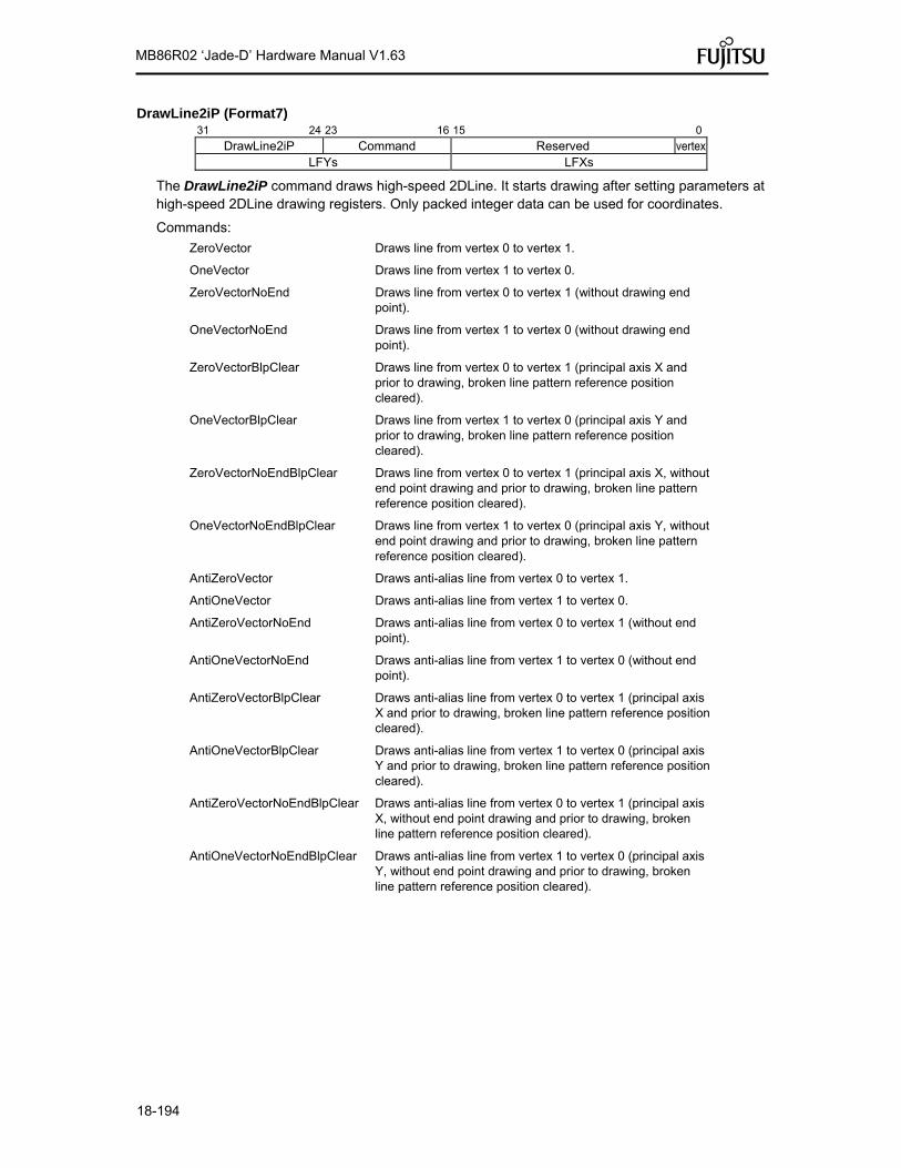
18-194
MB86R02 ‘Jade-D’ Hardware Manual V1.63
DrawLine2iP (Format7) 31 24 23 16 15 0
DrawLine2iP Command Reserved vertex LFYs LFXs
The DrawLine2iP command draws high-speed 2DLine. It starts drawing after setting parameters at high-speed 2DLine drawing registers. Only packed integer data can be used for coordinates.
Commands:
ZeroVector Draws line from vertex 0 to vertex 1.
OneVector Draws line from vertex 1 to vertex 0.
ZeroVectorNoEnd Draws line from vertex 0 to vertex 1 (without drawing end point).
OneVectorNoEnd Draws line from vertex 1 to vertex 0 (without drawing end point).
ZeroVectorBlpClear Draws line from vertex 0 to vertex 1 (principal axis X and prior to drawing, broken line pattern reference position cleared).
OneVectorBlpClear Draws line from vertex 1 to vertex 0 (principal axis Y and prior to drawing, broken line pattern reference position cleared).
ZeroVectorNoEndBlpClear Draws line from vertex 0 to vertex 1 (principal axis X, without end point drawing and prior to drawing, broken line pattern reference position cleared).
OneVectorNoEndBlpClear Draws line from vertex 1 to vertex 0 (principal axis Y, without end point drawing and prior to drawing, broken line pattern reference position cleared).
AntiZeroVector Draws anti-alias line from vertex 0 to vertex 1.
AntiOneVector Draws anti-alias line from vertex 1 to vertex 0.
AntiZeroVectorNoEnd Draws anti-alias line from vertex 0 to vertex 1 (without end point).
AntiOneVectorNoEnd Draws anti-alias line from vertex 1 to vertex 0 (without end point).
AntiZeroVectorBlpClear Draws anti-alias line from vertex 0 to vertex 1 (principal axis X and prior to drawing, broken line pattern reference position cleared).
AntiOneVectorBlpClear Draws anti-alias line from vertex 1 to vertex 0 (principal axis Y and prior to drawing, broken line pattern reference position cleared).
AntiZeroVectorNoEndBlpClear Draws anti-alias line from vertex 0 to vertex 1 (principal axis X, without end point drawing and prior to drawing, broken line pattern reference position cleared).
AntiOneVectorNoEndBlpClear Draws anti-alias line from vertex 1 to vertex 0 (principal axis Y, without end point drawing and prior to drawing, broken line pattern reference position cleared).

18-195
MB86R02 ‘Jade-D’ Hardware Manual V1.63
DrawTrap (Format5) 31 24 23 16 15 0
DrawTrap Command Reserved Ys 0
Xs DXdy XUs
DXUdy XLs
DXLdy USN 0 LSN 0
The DrawTrap command draws Triangle. It starts drawing after setting parameters at the Triangle Drawing registers (coordinates).
Commands:
TrapRight Draws right triangle.
TrapLeft Draws left triangle.
DrawVertex2i (Format7) 31 24 23 16 15 0
DrawVertex2i Command Reserved vertex Xdc 0 Ydc 0
The DrawVertex2i command draws high-speed 2DTriangle
It starts triangle drawing after setting parameters at 2DTriangle Drawing registers.
Commands:
TriangleFan Draws high-speed 2DTriangle.
FlagTriangleFan Draws high-speed 2DTriangle for polygon drawing in the flag buffer.
DrawVertex2iP (Format7) 31 24 23 16 15 0
DrawVertex2iP Command Reserved vertex Ydc Xdc
The DrawVertex2iP command draws high-speed 2DTriangle
It starts drawing after setting parameters at 2DTriangle Drawing registers
Only the packed integer format can be used for vertex coordinates.
Commands:
TriangleFan Draw high-speed 2DTriangle.
FlagTriangleFan Draws high-speed 2DTriangle for polygon drawing in the flag buffer.

18-196
MB86R02 ‘Jade-D’ Hardware Manual V1.63
DrawRectP (Format5) 31 24 23 16 15 0
DrawRectP Command Reserved RYs RXs
RsizeY RsizeX
The DrawRectP command fills rectangle. The rectangle is filled with the current color after setting parameters at the rectangle registers. Please set XRES(X resolution) to in 8 byte units when using this command.
Commands:
BltFill Fills rectangle with current color (single).
ClearPolyFlag Fills polygon drawing flag buffer area with 0. The size of drawing frame is defined in RsizeX,Y.
Must set RXs[3:0] and RsizeX[3:0] as 0000. (16pixel aligned)
Drawing clipping is not work for this command.
DrawBitmapP (Format6) 31 24 23 16 15 0
DrawBitmapP Command Count RYs RXs
RsizeY RsizeX (Pattern 0) (Pattern 1)
(Pattern n)
The DrawBitmapP command draws rectangle patterns. Please set XRES(X resolution) to in 8 byte units when using this command.
Commands:
BltDraw Draws rectangle of 8 bits/pixel or 16 bits/pixel.
DrawBitmap Draws binary bitmap character pattern. Bit 0 is drawn in transparent or background color and bit 1 is drawn in foreground color.
The “RsizeX” has to be up to 2016 in this command.
DrawBitmapLargeP (Format11) 31 24 23 16 15 0
DrawBitmapLargeP Command Reserved Count
Rys Rxs RsizeY RsizeX
(Pattern 0) (Pattern 1)
(Pattern n)
The DrawBitmapP command draws rectangle patterns.
The parameter(count field) could be used up to 32-bit(*1) unlike DrawBitmapP.
(*1: The data format of counter field is signed long. Thus actually it is possible to use up to 31-bit.)
Please set XRES(X resolution) to in 8 byte units when using this command.
Commands:
BltDraw Draws rectangle of 8 bits/pixel or 16 bits/pixel.
BltCopyP (Format5)

18-197
MB86R02 ‘Jade-D’ Hardware Manual V1.63
31 24 23 16 15 0
BltCopyP Command Reserved SRYs SRXs DRYs DRXs
BRsizeY BRsizeX
The BltCopyP command copies rectangle pattern within drawing frame. Please set XRES(X resolution) to in 8 byte units when using this command.
Commands:
TopLeft Starts BitBlt transfer from top left coordinates.
TopRight Starts BitBlt transfer from top right coordinates.
BottomLeft Starts BitBlt transfer from bottom left coordinates.
BottomRight Starts BitBlt transfer from bottom right coordinates.
BltCopyAlternateP (Format5) 31 24 23 16 15 0
BltCopyAlternateP Command Reserved SADDR SStride
SRYs SRXs DADDR DStride
DRYs DRXs BRsizeY BRsizeX
The BltCopyAlternateP command copies rectangle between two separate drawing frames.
Please set XRES(X resolution) to in 8 byte units when using this command. And please set SStride and DStride to in 8 byte units.
The actual address of a source address for VRAM is calculated by adding the segment address of FBR to SADDR.
The actual address of a destination address for VRAM is calculated by adding the segment address of FBR to DADDR.
Command:
TopLeft Starts BitBlt transfer from top left coordinates.
Drawing clipping is not wok for this command.
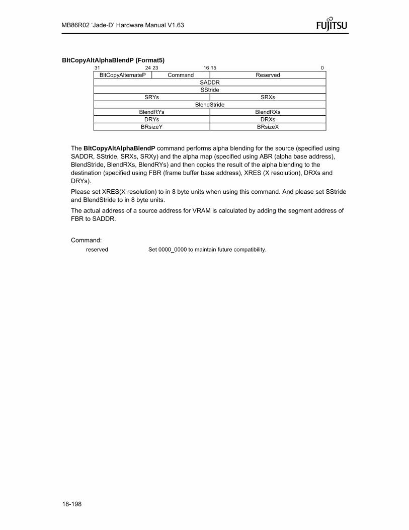
18-198
MB86R02 ‘Jade-D’ Hardware Manual V1.63
BltCopyAltAlphaBlendP (Format5) 31 24 23 16 15 0
BltCopyAlternateP Command Reserved SADDR SStride
SRYs SRXs BlendStride
BlendRYs BlendRXs DRYs DRXs
BRsizeY BRsizeX
The BltCopyAltAlphaBlendP command performs alpha blending for the source (specified using SADDR, SStride, SRXs, SRXy) and the alpha map (specified using ABR (alpha base address), BlendStride, BlendRXs, BlendRYs) and then copies the result of the alpha blending to the destination (specified using FBR (frame buffer base address), XRES (X resolution), DRXs and DRYs).
Please set XRES(X resolution) to in 8 byte units when using this command. And please set SStride and BlendStride to in 8 byte units.
The actual address of a source address for VRAM is calculated by adding the segment address of FBR to SADDR.
Command:
reserved Set 0000_0000 to maintain future compatibility.

18-199
MB86R02 ‘Jade-D’ Hardware Manual V1.63
18.11.4 Drawing Engine / Geometry Engine Register summary
18.11.4.1 Drawing Engine register list
The parenthesized value in the Offset field denotes the absolute address used by the SetRegister command.
BaseAddress = DrawBaseAddress (=0xF1FF_0000)
Offset 31 30 29 28 27 26 25 24 23 22 21 20 19 18 17 16 15 14 13 12 11 10 9 8 7 6 5 4 3 2 1 0
000
(000)
Ys
S S S S Int Frac
004
(001)
Xs
S S S S Int Frac
008
(002)
dXdy
S S S S Int Frac
00C
(003)
XUs
S S S S Int Frac
010
(004)
dXUdy
S S S S Int Frac
014
(005)
XLs
S S S S Int Frac
018
(006)
dXLdy
S S S S Int Frac
01C
(007)
USN
0 0 0 0 Int 0
020
(008)
LSN
0 0 0 0 Int 0
040
(010)
Rs
0 0 0 0 0 0 0 0 Int Frac
044
(011)
dRdx
S S S S S S S S Int Frac
048
(012)
dRdy
S S S S S S S S Int Frac
04C
(013)
Gs
0 0 0 0 0 0 0 0 Int Frac
050
(014)
dGdx
S S S S S S S S Int Frac
054
(015)
dGdy
S S S S S S S S Int Frac
058
(016)
Bs
0 0 0 0 0 0 0 0 Int Frac
05C dBdx

18-200
MB86R02 ‘Jade-D’ Hardware Manual V1.63
(017) S S S S S S S S Int Frac
060
(018)
dBdy
S S S S S S S S Int Frac

18-201
MB86R02 ‘Jade-D’ Hardware Manual V1.63
Offset 31 30 29 28 27 26 25 24 23 22 21 20 19 18 17 16 15 14 13 12 11 10 9 8 7 6 5 4 3 2 1 0
080
(020)
Zs
0 Int Frac
084
(021)
dZdx
S Int Frac
088
(022)
dZdy
S Int Frac
0C0
(030)
Ss
S S S Int Frac
0C4
(031)
dSdx
S S S Int Frac
0C8
(032)
dSdy
S S S Int Frac
0CC
(033)
Ts
S S S Int Frac
0D0
(034)
dTdx
S S S Int Frac
0D4
(035)
dTdy
S S S Int Frac
0D8
(036)
Qs
0 0 0 0 0 0 0 INT
Frac
0DC
(037)
dQdx
S S S S S S S INT
Frac
0E0
(038)
dQdy
S S S S S S S INT
Frac
140
(050)
LPN
0 0 0 0 Int 0
144
(051)
LXs
S S S S Int Frac
148
(052)
LXde
S S S S S S S S S S S S S S S Int
Frac
14C
(053)
LYs
S S S S Int Frac
150
(054)
LYde
S S S S S S S S S S S S S S S Int
Frac
154
(055)
LZs
S Int Frac
158
(056)
LZde
S Int Frac

18-202
MB86R02 ‘Jade-D’ Hardware Manual V1.63
Offset 31 30 29 28 27 26 25 24 23 22 21 20 19 18 17 16 15 14 13 12 11 10 9 8 7 6 5 4 3 2 1 0
180
(060)
PXdc
S S S S Int Frac
184
(061)
PYdc
S S S S Int Frac
188
(062)
PZdc
S Int Frac
200
(080)
RXs
S S S S Int 0
204
(081)
RYs
S S S S Int 0
208
(082)
RsizeX
S S S S Int 0
20C
(083)
RsizeY
S S S S Int 0
240
(090)
SADDR
0 0 0 0 0 0 0 Address
244
(091)
SStride
0 0 0 0 Int 0
248
(092)
SRXs
0 0 0 0 Int 0
24C
(093)
SRYs
0 0 0 0 Int 0
250
(094)
DADDR
0 0 0 0 0 0 0 Address
254
(095)
DStride
0 0 0 0 Int 0
258
(096)
DRXs
0 0 0 0 Int 0
25C
(097)
DRYs
0 0 0 0 Int 0
260
(098)
BRsizeX
0 0 0 0 Int 0
264
(099)
BRsizeY
0 0 0 0 Int 0
268
(09A)
TColor
0 Color
3E0
(0f8)
BLPO
BCR

18-203
MB86R02 ‘Jade-D’ Hardware Manual V1.63
Offset 31 30 29 28 27 26 25 24 23 22 21 20 19 18 17 16 15 14 13 12 11 10 9 8 7 6 5 4 3 2 1 0
400
(100)
CTR
FD
FE
CE
FCNT NF
FF
FE
SS DS PS
404
()
IFSR
FD
FE
C
E
408
()
IFCNT
FCNT
40C
()
SST
SS
410
()
DS
DS
414
()
PST
PS
418
()
EST
FD
PE
C
E
420
(108)
MDR0
FS
ZP
CF
CY
CX
BSV BSH
424
(109)
MDR1/MDR1S/MDR1B/MDR1TL
LW
BP
BL LOG BM ZW
ZCL ZC
AS
SM
428
(10a)
MDR2/MDR2S/MDR2TL
TT LOG BM ZW
ZCL Z
C
AS
SM
42C
(10b)
MDR3
BA
TAB
TBL
TWS TWT
TF
TC
430
(10c)
MDR4
LOG BM
TE
43C
(10f)
MDR7
LTH
EZ
GG
PG
H
PT
H
PZ
H

18-204
MB86R02 ‘Jade-D’ Hardware Manual V1.63
Offset 31 30 29 28 27 26 25 24 23 22 21 20 19 18 17 16 15 14 13 12 11 10 9 8 7 6 5 4 3 2 1 0
440
(110)
FBR
FBASE
444
(111)
XRES XRES
448
(112)
ZBR
ZBASE
44C
(113)
TBR
TBASE
450
(114)
PFBR
PFBASE
454
(115)
CXMIN
CLIPXMIN
458
(116)
CXMAX
CLIPXMAX
45C
(117)
CYMIN
CLIPYMIN
460
(118)
CYMAX
CLIPYMAX
464
(119)
TXS
TXSN TXSM
468
(11a)
TIS
TISN TISM
46C
(11b)
TOA
XBO
470
(11C)
SHO
SHOFFS
474
(11D)
ABR
ABASE
480
(120)
FC
FGC8/16/24
484
(121)
BC
BGC8/16/24
488
(122)
ALF
A
48C
(123) BLP
494
(129)
TBC
BC16/24
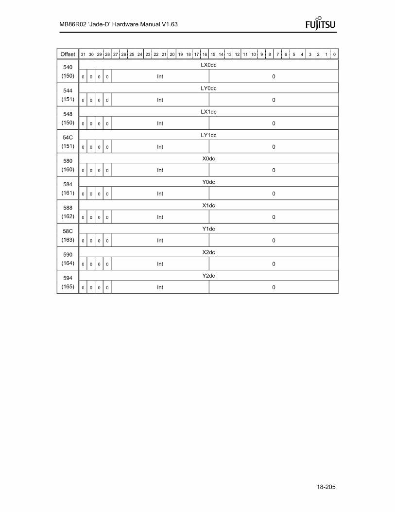
18-205
MB86R02 ‘Jade-D’ Hardware Manual V1.63
Offset 31 30 29 28 27 26 25 24 23 22 21 20 19 18 17 16 15 14 13 12 11 10 9 8 7 6 5 4 3 2 1 0
540
(150)
LX0dc
0 0 0 0 Int 0
544
(151)
LY0dc
0 0 0 0 Int 0
548
(150)
LX1dc
0 0 0 0 Int 0
54C
(151)
LY1dc
0 0 0 0 Int 0
580
(160)
X0dc
0 0 0 0 Int 0
584
(161)
Y0dc
0 0 0 0 Int 0
588
(162)
X1dc
0 0 0 0 Int 0
58C
(163)
Y1dc
0 0 0 0 Int 0
590
(164)
X2dc
0 0 0 0 Int 0
594
(165)
Y2dc
0 0 0 0 Int 0
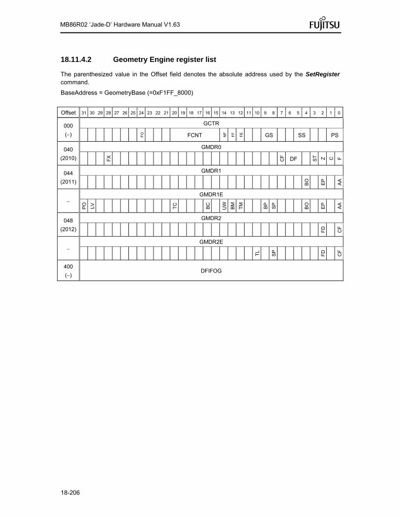
18-206
MB86R02 ‘Jade-D’ Hardware Manual V1.63
18.11.4.2 Geometry Engine register list
The parenthesized value in the Offset field denotes the absolute address used by the SetRegister command.
BaseAddress = GeometryBase (=0xF1FF_8000)
Offset 31 30 29 28 27 26 25 24 23 22 21 20 19 18 17 16 15 14 13 12 11 10 9 8 7 6 5 4 3 2 1 0
000
()
GCTR
FO
FCNT NF
FF
FE
GS SS PS
040
(2010)
GMDR0
FX
CF
DF
ST
Z
C
F
044
(2011)
GMDR1
BO
EP
AA
GMDR1E
PO
LV
TC
BC
UW
BM
TM
BP
SP
BO
EP
AA
048
(2012)
GMDR2
FD
CF
GMDR2E
TL
SP
FD
CF
400
() DFIFOG

18-207
MB86R02 ‘Jade-D’ Hardware Manual V1.63
18.11.5 Drawing control registers
CTR (Control Register) Register address
DrawBaseAddress + 400H
Bit number 31 30 29 28 27 26 25 24 23 22 21 20 19 18 17 16 15 14 13 12 11 10 9 8 7 6 5 4 3 2 1 0
Bit field name FO CE FCNT NF FF FE SS DS PS
R/W RW RW R R R R R R R
Initial value 0 0 011101 0 0 1 00 00 00
This register indicates drawing flags and status information. Bits 24 to 22 are not cleared until 0 is set.
Bit 1 and 0 PS (Pixel engine Status)
Indicate status of pixel engine unit
00 Idle
01 Busy
10 Reserved
11 Reserved
Bit 5 and 4 DS (DDA Status)
Indicate status of DDA
00 Idle
01 Busy
10 Busy
11 Reserved
Bit 9 and 8 SS (Setup Status)
Indicate status of Setup unit
00 Idle
01 Busy
10 Reserved
11 Reserved
Bit 12 FE (FIFO Empty)
Indicates whether data contained or not in display list FIFO
0 Valid data
1 No valid data
Bit 13 FF (FIFO Full)
Indicates whether display list FIFO is full or not
0 Not full
1 Full
Bit 14 NF (FIFO Near Full)
Indicates how empty the display list FIFO is

18-208
MB86R02 ‘Jade-D’ Hardware Manual V1.63
0 Empty entries equal to or more than half
1 Empty entries less than half
Bit 20 to 15 FCNT (FIFO Counter)
Indicates count of empty entries of display list FIFO (0 to 100000H)
Bit 22 CE (Display List Command Error)
Indicates command error occurrence (Not all error can detect. Requires software reset or hardware reset for recovery)
0 Normal
1 Command error detected
Bit 24 FO (FIFO Overflow)
Indicates FIFO overflow occurrence
0 Normal
1 FIFO overflow detected
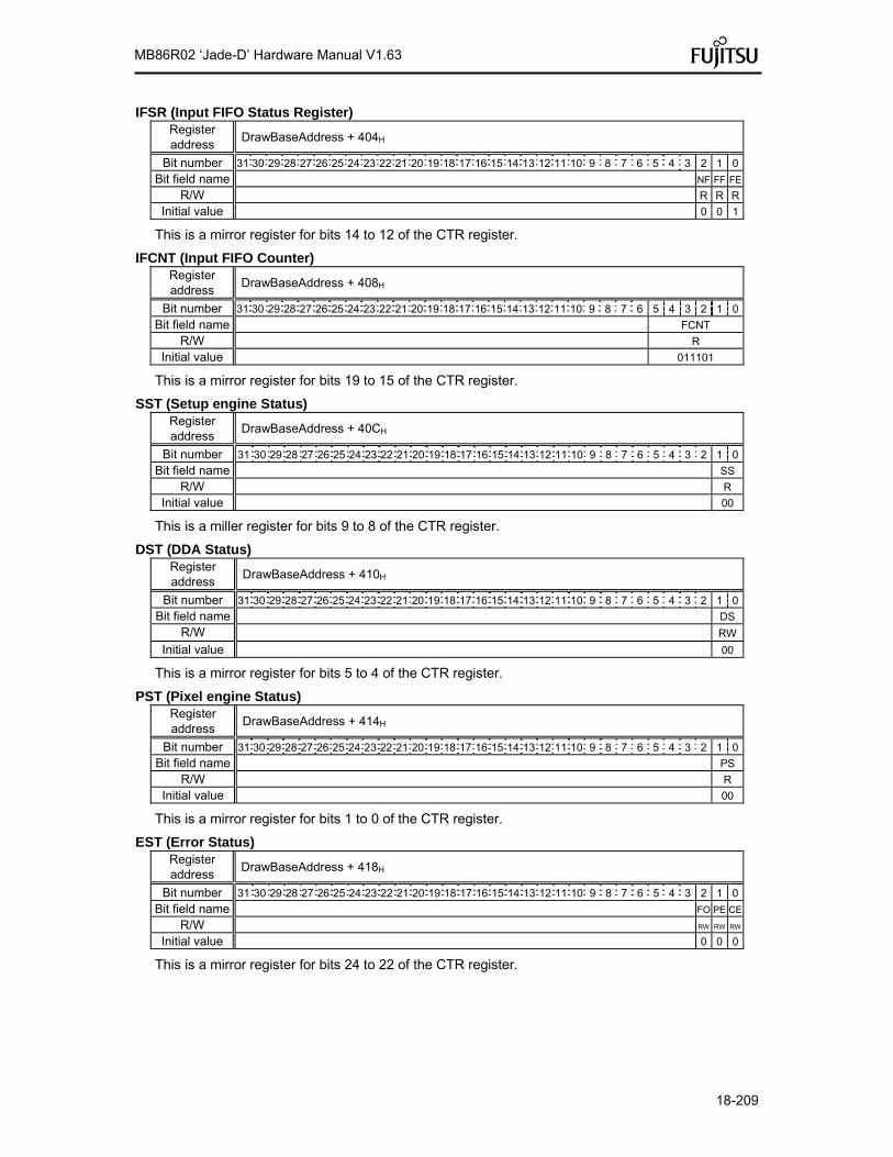
18-209
MB86R02 ‘Jade-D’ Hardware Manual V1.63
IFSR (Input FIFO Status Register) Register address
DrawBaseAddress + 404H
Bit number 31 30 29 28 27 26 25 24 23 22 21 20 19 18 17 16 15 14 13 12 11 10 9 8 7 6 5 4 3 2 1 0
Bit field name NF FF FE
R/W R R R
Initial value 0 0 1
This is a mirror register for bits 14 to 12 of the CTR register.
IFCNT (Input FIFO Counter) Register address
DrawBaseAddress + 408H
Bit number 31 30 29 28 27 26 25 24 23 22 21 20 19 18 17 16 15 14 13 12 11 10 9 8 7 6 5 4 3 2 1 0
Bit field name FCNT
R/W R
Initial value 011101
This is a mirror register for bits 19 to 15 of the CTR register.
SST (Setup engine Status) Register address
DrawBaseAddress + 40CH
Bit number 31 30 29 28 27 26 25 24 23 22 21 20 19 18 17 16 15 14 13 12 11 10 9 8 7 6 5 4 3 2 1 0
Bit field name SS
R/W R
Initial value 00
This is a miller register for bits 9 to 8 of the CTR register.
DST (DDA Status) Register address
DrawBaseAddress + 410H
Bit number 31 30 29 28 27 26 25 24 23 22 21 20 19 18 17 16 15 14 13 12 11 10 9 8 7 6 5 4 3 2 1 0
Bit field name DS
R/W RW
Initial value 00
This is a mirror register for bits 5 to 4 of the CTR register.
PST (Pixel engine Status) Register address
DrawBaseAddress + 414H
Bit number 31 30 29 28 27 26 25 24 23 22 21 20 19 18 17 16 15 14 13 12 11 10 9 8 7 6 5 4 3 2 1 0
Bit field name PS
R/W R
Initial value 00
This is a mirror register for bits 1 to 0 of the CTR register.
EST (Error Status) Register address
DrawBaseAddress + 418H
Bit number 31 30 29 28 27 26 25 24 23 22 21 20 19 18 17 16 15 14 13 12 11 10 9 8 7 6 5 4 3 2 1 0
Bit field name FO PE CE
R/W RW RW RW
Initial value 0 0 0
This is a mirror register for bits 24 to 22 of the CTR register.

18-210
MB86R02 ‘Jade-D’ Hardware Manual V1.63
18.11.6 Drawing mode registers
When write to the registers, use the SetRegister command. The registers cannot be accessed from the CPU.
MDR0 (Mode Register for miscellaneous) Register address
DrawBaseAddress + 420H
Bit number 31 30 29 28 27 26 25 24 23 22 21 20 19 18 17 16 15 14 13 12 11 10 9 8 7 6 5 4 3 2 1 0
Bit field name FS ZP CF CY CX BSV BSH
R/W R/W RW RW RW RW RW RW
Initial value 00 0 00 0 0 00 00
Bit 1 to 0 BSH (Bitmap Scale Horizontal)
Sets horizontal zoom ratio of bitmap draw
00 x1
01 x2
10 x1/2
01 Reserved
Bit 3 to 2 BSV (Bitmap Scale Vertical)
Sets vertical zoom ratio of bitmap draw
00 x1
01 x2
10 x1/2
01 Reserved
Bit 8 CX (Clip X enable)
Sets X coordinates clipping mode
0 Disabled
1 Enabled
Bit 9 CY (Clip Y enable)
Sets Y coordinates clipping mode
0 Disabled
1 Enabled
Bit 16 and 15 CF (Color Format)
Sets drawing color format
00 Indirect color mode (8 bits/pixel)
01 Direct color mode (16 bits/pixel)
Bit 20 ZP (Z Precision)
Sets the precision of the Z value used for erasing hidden planes.
16 bits/pixel
8 bits/pixel

18-211
MB86R02 ‘Jade-D’ Hardware Manual V1.63
Bit30-29 FS (Frame Select for Sync[rendering command])
00 FRAME0 (initial value) Synchronize with FRAME0
01 FRAME1 Synchronize with FRAME1
10 RESERVED -
11 RESERVED -

18-212
MB86R02 ‘Jade-D’ Hardware Manual V1.63
MDR1/MDR1S/MDR1B (Mode Register for LINE/for Shadow/for Border) Register address
DrawBaseAddress + 424H
Bit number 31 30 29 28 27 26 25 24 23 22 21 20 19 18 17 16 15 14 13 12 11 10 9 8 7 6 5 4 3 2 1 0
Bit field name LW BP BL LOG BM ZW ZCL ZC AS
R/W RW RW RW RW RW RW RW RW RW
Initial value 00000 0 0 0011 0 0 0000 0 0
This register sets the mode of line and pixel drawing.
This register is used for the body primitive, for the shade primitive, for the edge primitive.
The value after a drawing that involves the shade primitive, the edge primitive, or the top-left non-applicable primitive is the value set for MDR1.
Please set ZC bit (bit 2) to 0 when draw BltCopyAltAlphaBlendP command.
Bit 1 AS (Alpha Shading mode)
Sets the shading mode for alpha.
0 Alpha flat shading
1 Alpha Gouraud shading
Bit 2 ZC (Z Compare mode)
Sets Z comparison mode
0 Disabled
1 Enabled
Bit 5 to 3 ZCL (Z Compare Logic)
Selects type of Z comparison
000 NEVER
001 ALWAYS
010 LESS
011 LEQUAL
100 EQUAL
101 GEQUAL
110 GREATER
111 NOTEQUAL
Bit 6 ZW (Z Write mode)
Sets Z write mode
0 Writes Z values.
1 Not write Z values.
Bit 8 to 7 BM (Blend Mode)
Sets blend mode
00 Normal (source copy)
01 Alpha blending
10 Drawing with logic operation
11 Reserved

18-213
MB86R02 ‘Jade-D’ Hardware Manual V1.63
Bit 12 to 9 LOG (Logical operation)
Sets type of logic operation
0000 CLEAR
0001 AND
0010 AND REVERSE
0011 COPY
0100 AND INVERTED
0101 NOP
0110 XOR
0111 OR
1000 NOR
1001 EQUIV
1010 INVERT
1011 OR REVERSE
1100 COPY INVERTED
1101 OR INVERTED
1110 NAND
1111 SET
Bit 19 BL (Broken Line)
Selects line type
0 Solid line
1 Broken line
Bit 20 BP (Broken line Period)
Selects broken line cycle
0: 32 bits
1: 24 bits
Bit 28 to 24 LW (Line Width)
Sets line width for drawing line
00000 1 pixel
00001 2 pixels
: :
11111 32 pixels

18-214
MB86R02 ‘Jade-D’ Hardware Manual V1.63
MDR2/MDR2S/MDR2TL (Mode Register for Polygon/for Shadow/for TopLeft) Register address
DrawBaseAddress + 428H
Bit number 31 30 29 28 27 26 25 24 23 22 21 20 19 18 17 16 15 14 13 12 11 10 9 8 7 6 5 4 3 2 1 0
Bit field name TT LOG BM ZW ZCL ZC AS SM
R/W RW RW RW RW RW RW RW RW
Initial value 00 0011 0 0 0000 0 0 0
This register sets the polygon drawing mode.
This register is used for the body primitive, for the shade primitive and for the top-left non-applicable primitive.
The value after a drawing that involves the shade primitive or the top-left non-applicable primitive is the value set for MDR2.
(Must set SM=AS=TT=0 for MDR2S)
Bit 0 SM (Shading Mode)
Sets shading mode
0 Flat shading
1 Gouraud shading
Bit 1 AS (Alpha Shading mode)
Sets alpha shading mode. This mode is enabled for only alpha.
0 Alpha flat shading
1 Alpha gouraud shading
Bit 2 ZC (Z Compare mode)
Sets Z comparison mode
0 Disabled
1 Enabled
Bit 5 to 3 ZCL (Z Compare Logic)
Selects type of Z comparison
000 NEVER
001 ALWAYS
010 LESS
011 LEQUAL
100 EQUAL
101 GEQUAL
110 GREATER
111 NOTEQUAL
Bit 6 ZW (Z Write mask)
Sets Z write mode
0 Writes Z values
1 Not write Z values

18-215
MB86R02 ‘Jade-D’ Hardware Manual V1.63
Bit 8 to 7 BM (Blend Mode)
Sets blend mode
00 Normal (source copy)
01 Alpha blending
10 Drawing with logic operation
11 Reserved
Bit 12 to 9 LOG (Logical operation)
Sets type of logic operation
0000 CLEAR
0001 AND
0010 AND REVERSE
0011 COPY
0100 AND INVERTED
0101 NOP
0110 XOR
0111 OR
1000 NOR
1001 EQUIV
1010 INVERT
1011 OR REVERSE
1100 COPY INVERTED
1101 OR INVERTED
1110 NAND
1111 SET
Bit 29 to 28 TT (Texture-Tile Select)
Selects texture or tile pattern
00 Neither used
01 Enabled tiling
10 Enabled texture
11 Reserved

18-216
MB86R02 ‘Jade-D’ Hardware Manual V1.63
MDR3 (Mode Register for Texture) Register address
DrawBaseAddress + 42CH
Bit number 31 30 29 28 27 26 25 24 23 22 21 20 19 18 17 16 15 14 13 12 11 10 9 8 7 6 5 4 3 2 1 0
Bit field name BA TAB TBL TWS TWT TF TC
R/W RW RW RW RW RW RW RW
Initial value 0 00 00 00 00 0 0
This register sets the texture mapping mode.
Bit 3 TC (Texture coordinates Correct)
Sets texture coordinates correction mode
0 Disabled
1 Enabled
Bit 5 TF (Texture Filtering)
Sets type of texture interpolation (filtering)
0 Point sampling
1 Bi-linear filtering
Bit 9 and 8 TWT (Texture Wrap T)
Sets type of texture coordinates T direction wrapping
00 Cramp
01 Repeat
10 Border
11 Reserved
Bit 11 and 10 TWS (Texture Wrap S)
Sets type of texture coordinates S direction wrapping
00 Cramp
01 Repeat
10 Border
11 Reserved
Bit 17 and 16 TBL (Texture Blend mode)
Sets texture blending mode
00 Decal
01 Modulate
10 Stencil
11 Reserved
Bit 21 and 20 TAB (Texture Alpha Blend mode)

18-217
MB86R02 ‘Jade-D’ Hardware Manual V1.63
Sets texture blending mode
The stencil mode and the stencil alpha mode are enabled only when the MDR2 register blend mode (BM) is set to the alpha blending mode. If it is not set to the alpha blending mode, the stencil mode and stencil alpha mode perform the same function as the normal mode.
00 Normal
01 Stencil
10 Stencil alpha
11 Reserved
Bit 24 BA (Bilinear Accelerate Mode)
Improves the performance of bi-linear filtering, although a texture area of four times the default texture area is used.
0 Default texture area used
1 Texture area four times default texture area used

18-218
MB86R02 ‘Jade-D’ Hardware Manual V1.63
MDR4 (Mode Register for BLT) Register address
DrawBaseAddress + 430H
Bit number 31 30 29 28 27 26 25 24 23 22 21 20 19 18 17 16 15 14 13 12 11 10 9 8 7 6 5 4 3 2 1 0
Bit field name LOG BM TE R/W RW RW RW
Initial value 0011 00 0
This register controls the BLT mode.
Bit 1 TE (Transparent Enable)
Sets transparent mode
0: Not perform transparent processing
1: Not draw pixels that corresponds to set transparent color in BLT (transparancy copy)
Note: Set the blend mode (BM) to normal.
Bit 8 to 7 BM (Blend Mode)
Sets blend mode
00 Normal (source copy)
01 Reserved
10 Drawing with logic operation
11 Reserved
Bit 12 to 9 LOG (Logical operation)
Sets logic operation
0000 CLEAR
0001 AND
0010 AND REVERSE
0011 COPY
0100 AND INVERTED
0101 NOP
0110 XOR
0111 OR
1000 NOR
1001 EQUIV
1010 INVERT
1011 OR REVERSE
1100 COPY INVERTED
1101 OR INVERTED
1110 NAND
1111 SET
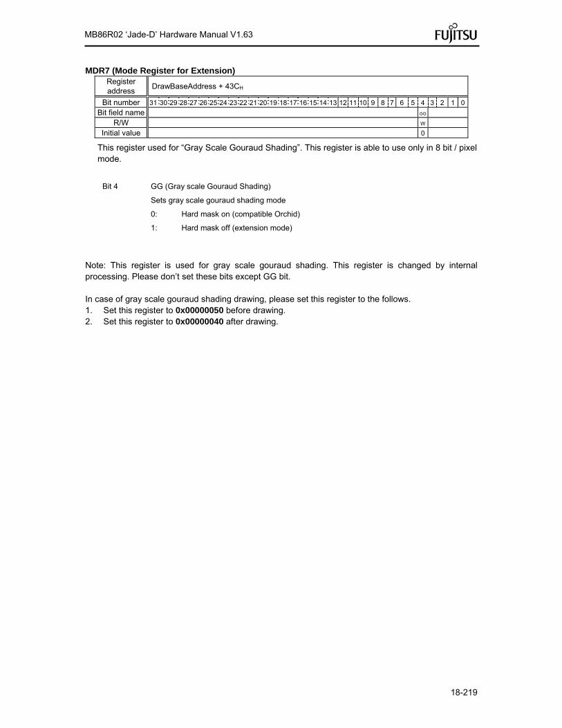
18-219
MB86R02 ‘Jade-D’ Hardware Manual V1.63
MDR7 (Mode Register for Extension) Register address
DrawBaseAddress + 43CH
Bit number 31 30 29 28 27 26 25 24 23 22 21 20 19 18 17 16 15 14 13 12 11 10 9 8 7 6 5 4 3 2 1 0
Bit field name GG
R/W W
Initial value 0
This register used for “Gray Scale Gouraud Shading”. This register is able to use only in 8 bit / pixel mode.
Bit 4 GG (Gray scale Gouraud Shading)
Sets gray scale gouraud shading mode
0: Hard mask on (compatible Orchid)
1: Hard mask off (extension mode)
Note: This register is used for gray scale gouraud shading. This register is changed by internal processing. Please don’t set these bits except GG bit. In case of gray scale gouraud shading drawing, please set this register to the follows. 1. Set this register to 0x00000050 before drawing. 2. Set this register to 0x00000040 after drawing.
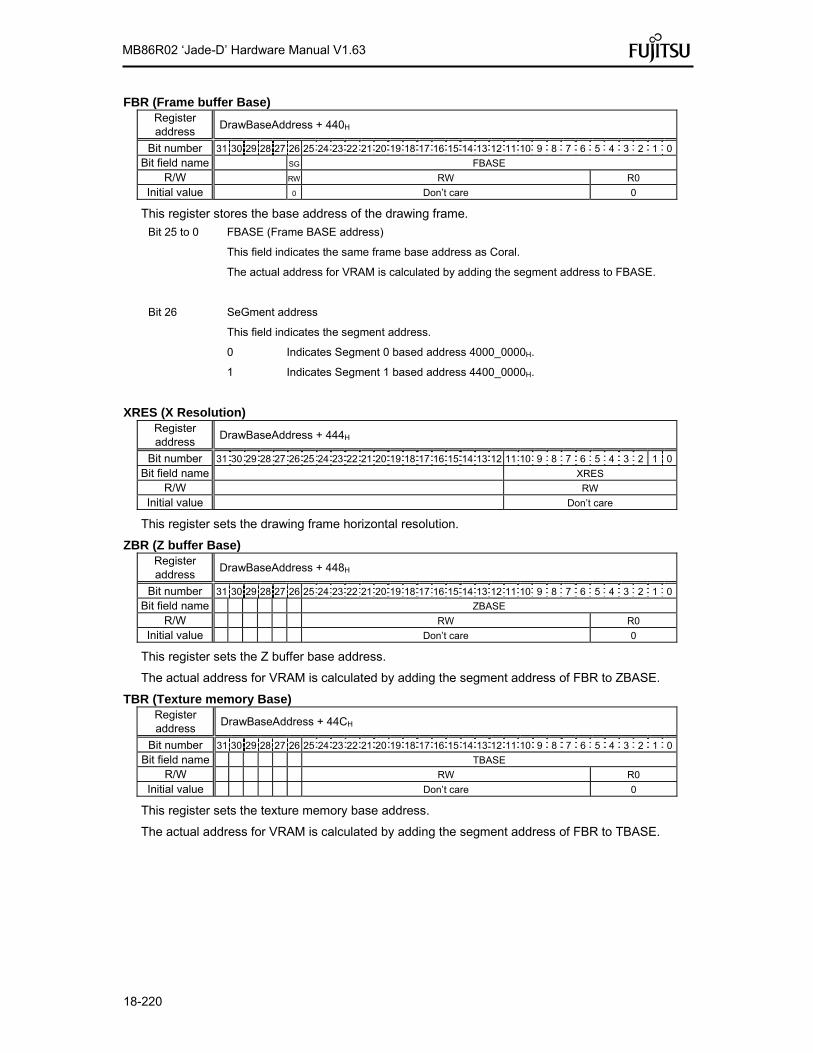
18-220
MB86R02 ‘Jade-D’ Hardware Manual V1.63
FBR (Frame buffer Base) Register address
DrawBaseAddress + 440H
Bit number 31 30 29 28 27 26 25 24 23 22 21 20 19 18 17 16 15 14 13 12 11 10 9 8 7 6 5 4 3 2 1 0
Bit field name SG FBASE
R/W RW RW R0
Initial value 0 Don’t care 0
This register stores the base address of the drawing frame.
Bit 25 to 0 FBASE (Frame BASE address)
This field indicates the same frame base address as Coral.
The actual address for VRAM is calculated by adding the segment address to FBASE.
Bit 26 SeGment address
This field indicates the segment address.
0 Indicates Segment 0 based address 4000_0000H.
1 Indicates Segment 1 based address 4400_0000H.
XRES (X Resolution) Register address
DrawBaseAddress + 444H
Bit number 31 30 29 28 27 26 25 24 23 22 21 20 19 18 17 16 15 14 13 12 11 10 9 8 7 6 5 4 3 2 1 0
Bit field name XRES
R/W RW
Initial value Don’t care
This register sets the drawing frame horizontal resolution.
ZBR (Z buffer Base) Register address
DrawBaseAddress + 448H
Bit number 31 30 29 28 27 26 25 24 23 22 21 20 19 18 17 16 15 14 13 12 11 10 9 8 7 6 5 4 3 2 1 0
Bit field name ZBASE
R/W RW R0
Initial value Don’t care 0
This register sets the Z buffer base address.
The actual address for VRAM is calculated by adding the segment address of FBR to ZBASE.
TBR (Texture memory Base) Register address
DrawBaseAddress + 44CH
Bit number 31 30 29 28 27 26 25 24 23 22 21 20 19 18 17 16 15 14 13 12 11 10 9 8 7 6 5 4 3 2 1 0
Bit field name TBASE
R/W RW R0
Initial value Don’t care 0
This register sets the texture memory base address.
The actual address for VRAM is calculated by adding the segment address of FBR to TBASE.

18-221
MB86R02 ‘Jade-D’ Hardware Manual V1.63
PFBR (2D Polygon Flag-Buffer Base) Register address
DrawBaseAddress + 450H
Bit number 31 30 29 28 27 26 25 24 23 22 21 20 19 18 17 16 15 14 13 12 11 10 9 8 7 6 5 4 3 2 1 0
Bit field name PFBASE
R/W RW R0
Initial value Don’t care 0
This register sets the polygon flag buffer base address.
The actual address for VRAM is calculated by adding the segment address of FBR to PFBASE.
CXMIN (Clip X minimum) Register address
DrawBaseAddress + 454H
Bit number 31 30 29 28 27 26 25 24 23 22 21 20 19 18 17 16 15 14 13 12 11 10 9 8 7 6 5 4 3 2 1 0
Bit field name CLIPXMIN
R/W RW
Initial value Don’t care
This register sets the clip frame minimum X position.
CXMAX (Clip X maximum) Register address
DrawBaseAddress + 458H
Bit number 31 30 29 28 27 26 25 24 23 22 21 20 19 18 17 16 15 14 13 12 11 10 9 8 7 6 5 4 3 2 1 0
Bit field name CLIPXMAX
R/W RW
Initial value Don’t care
This register sets the clip frame maximum X position.
CYMIN (Clip Y minimum) Register address
DrawBaseAddress + 45CH
Bit number 31 30 29 28 27 26 25 24 23 22 21 20 19 18 17 16 15 14 13 12 11 10 9 8 7 6 5 4 3 2 1 0
Bit field name CLIPYMIN
R/W RW
Initial value Don’t care
This register sets the clip frame minimum Y position.
CYMAX (Clip Y maximum) Register address
DrawBaseAddress + 460H
Bit number 31 30 29 28 27 26 25 24 23 22 21 20 19 18 17 16 15 14 13 12 11 10 9 8 7 6 5 4 3 2 1 0
Bit field name CLIPYMAX
R/W RW
Initial value Don’t care
This register sets the clip frame maximum Y position.

18-222
MB86R02 ‘Jade-D’ Hardware Manual V1.63
TXS (Texture Size) Register address
DrawBaseAddress + 464H
Bit number 31 30 29 28 27 26 25 24 23 22 21 20 19 18 17 16 15 14 13 12 11 10 9 8 7 6 5 4 3 2 1 0
Bit field name TXSN TXSM
R/W RW RW
Initial value 000010000000 000010000000
This register specifies the texture size (m, n).
Bit 12 to 0 TXSM (Texture Size M)
Sets horizontal texture size. Any power of 2 between 4 and 4096 can be used. Values that are not a power of 2 cannot be used.
0_0000_0000_0100 M=4 0_0010_0000_0000 M=512
0_0000_0000_1000 M=8 0_0100_0000_0000 M=1024
0_0000_0001_0000 M=16 0_1000_0000_0000 M=2048
0_0000_0010_0000 M=32 1_0000_0000_0000 M=4096
0_0000_0100_0000 M=64
0_0000_1000_0000 M=128
0_0001_0000_0000 M=256 Other than the above Setting disabled
Bit 28 to 16 TXSN (Texture Size N)
Sets vertical texture size. Any power of 2 between 4 and 4096 can be used. Values that are not a power of 2 cannot be used.
0_0000_0000_0100 N=4 0_0010_0000_0000 N=512
0_0000_0000_1000 N=8 0_0100_0000_0000 N=1024
0_0000_0001_0000 N=16 0_1000_0000_0000 N=2048
0_0000_0010_0000 N=32 1_0000_0000_0000 N=4096
0_0000_0100_0000 N=64
0_0000_1000_0000 N=128
0_0001_0000_0000 N=256 Other than the above Setting disabled
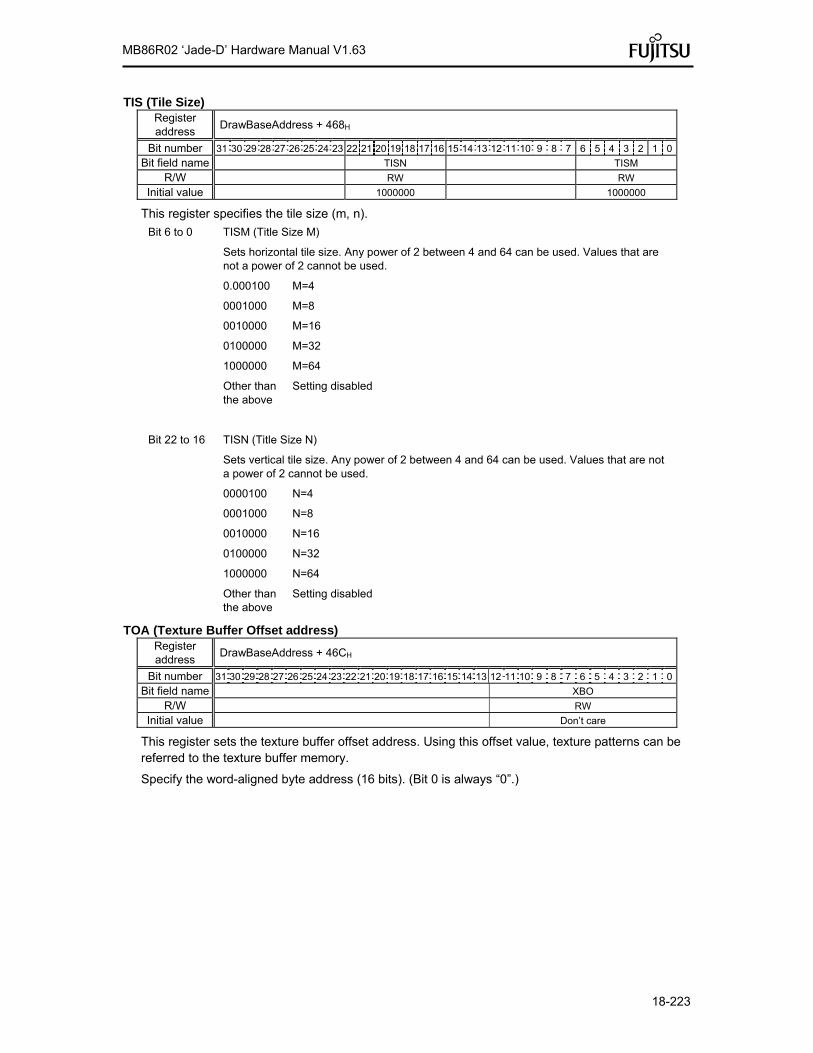
18-223
MB86R02 ‘Jade-D’ Hardware Manual V1.63
TIS (Tile Size) Register address
DrawBaseAddress + 468H
Bit number 31 30 29 28 27 26 25 24 23 22 21 20 19 18 17 16 15 14 13 12 11 10 9 8 7 6 5 4 3 2 1 0
Bit field name TISN TISM
R/W RW RW
Initial value 1000000 1000000
This register specifies the tile size (m, n).
Bit 6 to 0 TISM (Title Size M)
Sets horizontal tile size. Any power of 2 between 4 and 64 can be used. Values that are not a power of 2 cannot be used.
0.000100 M=4
0001000 M=8
0010000 M=16
0100000 M=32
1000000 M=64
Other than the above
Setting disabled
Bit 22 to 16 TISN (Title Size N)
Sets vertical tile size. Any power of 2 between 4 and 64 can be used. Values that are not a power of 2 cannot be used.
0000100 N=4
0001000 N=8
0010000 N=16
0100000 N=32
1000000 N=64
Other than the above
Setting disabled
TOA (Texture Buffer Offset address) Register address
DrawBaseAddress + 46CH
Bit number 31 30 29 28 27 26 25 24 23 22 21 20 19 18 17 16 15 14 13 12 11 10 9 8 7 6 5 4 3 2 1 0
Bit field name XBO
R/W RW
Initial value Don’t care
This register sets the texture buffer offset address. Using this offset value, texture patterns can be referred to the texture buffer memory.
Specify the word-aligned byte address (16 bits). (Bit 0 is always “0”.)

18-224
MB86R02 ‘Jade-D’ Hardware Manual V1.63
SHO (SHadow Offset) Register address
DrawBaseAddress + 470H
Bit number 31 30 29 28 27 26 25 24 23 22 21 20 19 18 17 16 15 14 13 12 11 10 9 8 7 6 5 4 3 2 1 0
Bit field name SHOFFS
R/W RW
Initial value Don’t care
This register sets the offset address of the shadow relative to the body primitive at drawing with shadow.
At body drawing, this offset address is set to “0”; at shadow drawing, the offset address calculated from each offset value of the X coordinates and of the Y coordinates is set. This register is hardware controlled.
ABR (Alpha map Base) Register address
DrawBaseAddress + 474H
Bit number 31 30 29 28 27 26 25 24 23 22 21 20 19 18 17 16 15 14 13 12 11 10 9 8 7 6 5 4 3 2 1 0
Bit field name ABASE
R/W RW R0
Initial value Don’t care 0
This register sets the base address of the alpha map.
The actual address for VRAM is calculated by adding the segment address of FBR to ABASE.
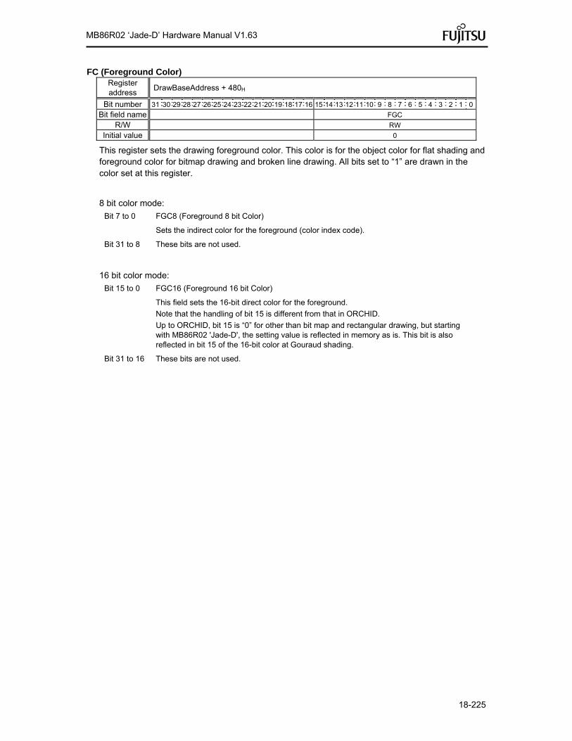
18-225
MB86R02 ‘Jade-D’ Hardware Manual V1.63
FC (Foreground Color) Register address
DrawBaseAddress + 480H
Bit number 31 30 29 28 27 26 25 24 23 22 21 20 19 18 17 16 15 14 13 12 11 10 9 8 7 6 5 4 3 2 1 0
Bit field name FGC
R/W RW
Initial value 0
This register sets the drawing foreground color. This color is for the object color for flat shading and foreground color for bitmap drawing and broken line drawing. All bits set to “1” are drawn in the color set at this register.
8 bit color mode:
Bit 7 to 0 FGC8 (Foreground 8 bit Color)
Sets the indirect color for the foreground (color index code).
Bit 31 to 8 These bits are not used.
16 bit color mode:
Bit 15 to 0 FGC16 (Foreground 16 bit Color)
This field sets the 16-bit direct color for the foreground.
Note that the handling of bit 15 is different from that in ORCHID.
Up to ORCHID, bit 15 is “0” for other than bit map and rectangular drawing, but starting with MB86R02 'Jade-D', the setting value is reflected in memory as is. This bit is also reflected in bit 15 of the 16-bit color at Gouraud shading.
Bit 31 to 16 These bits are not used.

18-226
MB86R02 ‘Jade-D’ Hardware Manual V1.63
BC (Background Color) Register address
DrawBaseAddress + 484H
Bit number 31 30 29 28 27 26 25 24 23 22 21 20 19 18 17 16 15 14 13 12 11 10 9 8 7 6 5 4 3 2 1 0
Bit field name BGC8/16/24
R/W RW
Initial value 0
This register sets the drawing frame background color. This color is used for the background color of bitmap drawing and broken line drawing. At bitmap drawing, all bits set to “0” are drawn in the color set at this register.
BT bit of this register allows the background color of be transparent (no drawing).
8 bit color mode:
Bit 7 to 0 BGC8 (Background 8 bit Color)
Sets the indirect color for the background (color index code)
Bit 14 to 8 Not used
Bit 15 BT (Background Transparency)
Sets the transparent mode for the background color
0 Background drawn using color set for BGC field
1 Background not drawn (transparent)
Bit 31 to 16 Not used
16 bit color mode:
Bit 14 to 0 BGC16 (Background 16 bit Color)
Sets 16-bit direct color (RGB) for the background
Bit 15 BT (Background Transparency)
Sets the transparent mode for the background color
0 Background drawn using color set for BGC field
1 Background not drawn (transparent)
Bit 31 to 16 Not used
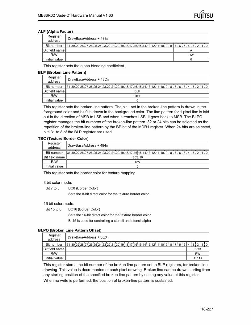
18-227
MB86R02 ‘Jade-D’ Hardware Manual V1.63
ALF (Alpha Factor) Register address
DrawBaseAddress + 488H
Bit number 31 30 29 28 27 26 25 24 23 22 21 20 19 18 17 16 15 14 13 12 11 10 9 8 7 6 5 4 3 2 1 0
Bit field name A
R/W RW
Initial value 0
This register sets the alpha blending coefficient.
BLP (Broken Line Pattern) Register address
DrawBaseAddress + 48CH
Bit number 31 30 29 28 27 26 25 24 23 22 21 20 19 18 17 16 15 14 13 12 11 10 9 8 7 6 5 4 3 2 1 0
Bit field name BLP
R/W RW
Initial value 0
This register sets the broken-line pattern. The bit 1 set in the broken-line pattern is drawn in the foreground color and bit 0 is drawn in the background color. The line pattern for 1 pixel line is laid out in the direction of MSB to LSB and when it reaches LSB, it goes back to MSB. The BLPO register manages the bit numbers of the broken-line pattern. 32 or 24 bits can be selected as the repetition of the broken-line pattern by the BP bit of the MDR1 register. When 24 bits are selected, bits 31 to 8 of the BLP register are used.
TBC (Texture Border Color) Register address
DrawBaseAddress + 494H
Bit number 31 30 29 28 27 26 25 24 23 22 21 20 19 18 17 16 15 14 13 12 11 10 9 8 7 6 5 4 3 2 1 0
Bit field name BC8/16
R/W RW
Initial value 0
This register sets the border color for texture mapping.
8 bit color mode:
Bit 7 to 0 BC8 (Border Color)
Sets the 8-bit direct color for the texture border color
16 bit color mode:
Bit 15 to 0 BC16 (Border Color)
Sets the 16-bit direct color for the texture border color
Bit15 is used for controlling a stencil and stencil alpha
BLPO (Broken Line Pattern Offset) Register address
DrawBaseAddress + 3E0H
Bit number 31 30 29 28 27 26 25 24 23 22 21 20 19 18 17 16 15 14 13 12 11 10 9 8 7 6 5 4 3 2 1 0
Bit field name BCR
R/W RW
Initial value 11111
This register stores the bit number of the broken-line pattern set to BLP registers, for broken line drawing. This value is decremented at each pixel drawing. Broken line can be drawn starting from any starting position of the specified broken-line pattern by setting any value at this register.
When no write is performed, the position of broken-line pattern is sustained.

18-228
MB86R02 ‘Jade-D’ Hardware Manual V1.63
18.11.7 Triangle drawing registers
Each register is used by the drawing commands. The registers cannot be accessed from the CPU or using the SetRegister command.
(XY coordinates register) Register Address 31 30 29 28 27 26 25 24 23 22 21 20 19 18 17 16 15 14 13 12 11 10 9 8 7 6 5 4 3 2 1 0
Ys 0000H S S S S Int Frac Xs 0004H S S S S Int Frac
dXdy 0008H S S S S Int Frac XUs 000cH S S S S Int Frac
dXUdy 0010H S S S S Int Frac XLs 0014H S S S S Int Frac
dXLdy 0018H S S S S Int Frac USN 001bH 0 0 0 0 Int 0 LSN 0020H 0 0 0 0 Int 0
Address Offset value from DrawBaseAddress S Sign bit or sign extension 0 Not used or 0 extension Int Integer or integer part of fixed point data Frac Fraction part of fixed point data
Sets (X, Y) coordinates for triangle drawing
Ys Y coordinates start position of long edge Xs X coordinates start position of long edge corresponding to Ys dXdy X DDA value of long edge direction XUs X coordinates start position of upper edge dXUdy X DDA value of upper edge direction XLs X coordinates start position of lower edge dXLdy X DDA value of lower edge direction USN Count of spans of upper triangle. If this value is “0”, the upper triangle is not drawn. LSN Count of spans of lower triangle. If this value is “0”, the lower triangle is not drawn.

18-229
MB86R02 ‘Jade-D’ Hardware Manual V1.63
(Color setting register) Register Address 31 30 29 28 27 26 25 24 23 22 21 20 19 18 17 16 15 14 13 12 11 10 9 8 7 6 5 4 3 2 1 0
Rs 0040H 0 0 0 0 0 0 0 0 Int Frac dRdx 0044H S S S S S S S S Int Frac dRdy 0048H S S S S S S S S Int Frac Gs 004CH 0 0 0 0 0 0 0 0 Int Frac
dGdx 0050H S S S S S S S S Int Frac dGdy 0054H S S S S S S S S Int Frac
Bs 0058H 0 0 0 0 0 0 0 0 Int Frac dBdx 005cH S S S S S S S S Int Frac dBdy 0060H S S S S S S S S Int Frac
As 0064H 0 0 0 0 0 0 0 0 Int Frac dAdx 0068H S S S S S S S S Int Frac dAdy 006cH S S S S S S S S Int Frac
Address Offset from DrawBaseAddress S Sign bit or sign extension 0 Not used or 0 extension Int Integer or integer part of fixed point data Frac Fraction part of fixed point data
Sets color parameters for triangle drawing. These parameters are enabled in the Gouraud shading mode.
Rs R value at (Xs, Ys, Zs) of long edge corresponding to Ys dRdx R DDA value of horizontal direction dRdy R DDA value of long edge Gs G value at (Xs, Ys, Zs) of long edge corresponding to Ys dGdx G DDA value of horizontal direction dGdy G DDA value of long edge Bs B value at (Xs, Ys, Zs) of long edge corresponding to Ys dBdx B DDA value of horizontal direction dBdy B DDA value of long edge As Alpha value at (Xs, Ys, Zs) of long edge corresponding to Ys dAdx Alpha DDA value of horizontal direction dAdy Alpha DDA value of long edge
(Z coordinates register) Register Address 31 30 29 28 27 26 25 24 23 22 21 20 19 18 17 16 15 14 13 12 11 10 9 8 7 6 5 4 3 2 1 0
Zs 0080h 0 Int Frac dZdx 0084h S Int Frac dZdy 008ch S Int Frac
Address Offset from DrawBaseAddress S Sign bit or sign extension 0 Not used or 0 extension Int Integer or integer part of fixed point data Frac Fraction part of fixed point data
Sets Z coordinates for 3D triangle drawing
Zs Z coordinate start position of long edge dZdx Z DDA value of horizontal direction dZdy Z DDA value of long edge
(Texture coordinates-setting register)

18-230
MB86R02 ‘Jade-D’ Hardware Manual V1.63
Register Address 31 30 29 28 27 26 25 24 23 22 21 20 19 18 17 16 15 14 13 12 11 10 9 8 7 6 5 4 3 2 1 0Ss 00c0H S S S Int Frac
dSdx 00c4H S S S Int Frac dSdy 00c8H S S S Int Frac
Ts 00ccH S S S Int Frac dTdx 00d0H S S S Int Frac dTdy 00d4H S S S Int Frac Qs 00d8H 0 0 0 0 0 0 0 Int Frac
dQdx 00dcH S S S S S S S Int Frac dQdy 00e0H S S S S S S S Int Frac
Address Offset from DrawBaseAddress S Sign bit or sign extension 0 Not used or 0 extension Int Integer or integer part of fixed point data Frac Fraction part of fixed point data
Sets texture coordinates parameters for triangle drawing
Ss S texture coordinates (Xs, Ys, Zs) of long edge corresponding to Ys dSdx S DDA value of horizontal direction dSdy S DDA value of long edge direction Ts T texture coordinates (Xs, Ys, Zs) of long edge corresponding to Ys dTdx T DDA value of horizontal direction dTdy T DDA value of long edge direction Qs Q (Perspective correction value) of texture at (Xs, Ys, Zs) of long edge corresponding to Ys dQdx Q DDA value of horizontal direction dQdy Q DDA value of long edge direction

18-231
MB86R02 ‘Jade-D’ Hardware Manual V1.63
18.11.8 Line drawing registers
Each register is used by the drawing commands. The registers cannot be accessed from the CPU or by using the SetRegister command.
(Coordinates setting register) Register Address 31 30 29 28 27 26 25 24 23 22 21 20 19 18 17 16 15 14 13 12 11 10 9 8 7 6 5 4 3 2 1 0LPN 0140H 0 0 0 0 Int 0 LXs 0144H S S S S Int Frac
LXde 0148H S S S S S S S S S S S S S S S Int Frac LYs 014cH S S S S Int Frac
LYde 0150H S S S S S S S S S S S S S S S Int Frac LZs 0154H S Int Frac
LZde 0158H S Int Frac
Address Offset from DrawBaseAddress S Sign bit or sign extension 0 Not used or 0 extension Int Integer or integer part of fixed point data Frac Fraction part of fixed point data
Sets coordinates parameters for line drawing
LPN Pixel count of principal axis direction
LXs X coordinates start position of draw line (In principal axis X) Integer value of X coordinates rounded off
(In principal axis Y) X coordinates in form of fixed point data
LXde Inclination data for X coordinates (In principal axis X) Increment or decrement according to drawing direction (In principal axis Y) Fraction part of DX/DY
LYs Y coordinates start position of draw line (In principal axis X) Y coordinates in form of fixed point data
(In principal axis Y) Integer value of Y coordinates rounded off
LYde Inclination data for Y coordinates (In principal axis X) Fraction part of DY/DX (In principal axis Y) Increment or decrement according to drawing direction
LZs Z coordinates start position of line drawing line
LZde Z Inclination

18-232
MB86R02 ‘Jade-D’ Hardware Manual V1.63
18.11.9 Pixel drawing registers
Each register is used by the drawing commands. The registers cannot be accessed from the CPU or using the SetRegister command.
Register Address 31 30 29 28 27 26 25 24 23 22 21 20 19 18 17 16 15 14 13 12 11 10 9 8 7 6 5 4 3 2 1 0PXdc 0180H 0 0 0 0 Int 0 PYdc 0184H 0 0 0 0 Int 0 PZdc 0188H 0 0 0 0 Int 0
Address Offset from DrawBaseAddress S Sign bit or sign extension 0 Not used or 0 extension Int Integer or integer part of fixed point data Frac Fraction part of fixed point data
Sets coordinates parameter for drawing pixel. The foreground color is used.
PXdc Sets X coordinates position PYdc Sets Y coordinates position PZdc Sets Z coordinates position
18.11.10 Rectangle drawing registers
Each register is used by the drawing commands. The registers cannot be accessed from the CPU or using the SetRegister command.
Register Address 31 30 29 28 27 26 25 24 23 22 21 20 19 18 17 16 15 14 13 12 11 10 9 8 7 6 5 4 3 2 1 0RXs 0200H 0 0 0 0 Int 0 RYs 0204H 0 0 0 0 Int 0
RsizeX 0208H 0 0 0 0 Int 0 RsizeY 020cH 0 0 0 0 Int 0
Address Offset from DrawBaseAddress S Sign bit or sign extension 0 Not used or 0 extension Int Integer or integer part of fixed point data Frac Fraction part of fixed point data
Sets coordinates parameters for rectangle drawing. The foreground color is used.
RXs Sets the X coordinates of top left vertex Rys Sets the Y coordinates of top left vertex RsizeX Sets horizontal size RsizeY Sets vertical size

18-233
MB86R02 ‘Jade-D’ Hardware Manual V1.63
18.11.11 Blt registers
Sets the parameters of each register as described below:
Set the Tcolor register with the SetRegister command.
Note that the Tcolor register cannot be set at access from the CPU and by drawing commands.
Each register except the Tcolor register is set by executing a drawing command.
Note that access from the CPU and the SetRegister command cannot be used.
Register Address 31 30 29 28 27 26 25 24 23 22 21 20 19 18 17 16 15 14 13 12 11 10 9 8 7 6 5 4 3 2 1 0SADDR 0240H 0 0 0 0 0 0 0 Address SStride 0244H 0 0 0 0 Int 0 SRXs 0248H 0 0 0 0 Int 0 SRYs 024cH 0 0 0 0 Int 0
DADDR 0250H 0 0 0 0 0 0 0 Address DStride 0254H 0 0 0 0 Int 0 DRXs 0258H 0 0 0 0 Int 0 DRYs 025cH 0 0 0 0 Int 0 BRsizeX 0260H 0 0 0 0 Int 0 BRsizeY 0264H 0 0 0 0 Int 0 TColor 0280H 0 Color BLPO 3E0CH BCR
Address Offset from DrawBaseAddress S Sign bit or sign extension 0 Not used or 0 extension Int Integer or integer part of fixed point data Frac Fraction part of fixed point data
Sets parameters for Blt operations
SADDR Sets start address of source rectangle area in byte address
SStride Sets stride of source
SRXs Sets X coordinates start position of source rectangle area
SRYs Sets Y coordinates start position of source rectangle area
DADDR Sets start address of destination rectangle area in byte address
DStride Sets stride of destination
DRXs Sets X coordinates start position of destination rectangle area
DRYs Sets Y coordinates start position of destination rectangle area
BRsizeX Sets horizontal size of rectangle
BRsizeY Sets vertical size of rectangle
Tcolor Sets transparent color
For indirect color, set a palette code in the lower 8 bits.

18-234
MB86R02 ‘Jade-D’ Hardware Manual V1.63
18.11.12 High-speed 2D line drawing registers
Each register is used by the drawing commands. The registers cannot be accessed from the CPU.
Register Address 31 30 29 28 27 26 25 24 23 22 21 20 19 18 17 16 15 14 13 12 11 10 9 8 7 6 5 4 3 2 1 0LX0dc 0540H 0 0 0 0 Int 0 LY0dc 0544H 0 0 0 0 Int 0 LX1dc 0548H 0 0 0 0 Int 0 LY1dc 054cH 0 0 0 0 Int 0
Address Offset from DrawBaseAddress S Sign bit or sign extension 0 Not used or 0 extension Int Integer or integer part of fixed point data Frac Fraction part of fixed point data
Sets coordinates of line end points for High-speed 2DLine drawing
LX0dc Sets X coordinates of vertex V0
LY0dc Sets Y coordinates of vertex V0
LX1dc Sets X coordinates of vertex V1
LY1dc Sets Y coordinates of vertex V1

18-235
MB86R02 ‘Jade-D’ Hardware Manual V1.63
18.11.13 High-speed 2D triangle drawing registers
Each register is used by the drawing commands. The registers cannot be accessed from the CPU or using the SetRegister command.
Register Address 31 30 29 28 27 26 25 24 23 22 21 20 19 18 17 16 15 14 13 12 11 10 9 8 7 6 5 4 3 2 1 0X0dc 0580h 0 0 0 0 Int 0 Y0dc 0584h 0 0 0 0 Int 0 X1dc 0588h 0 0 0 0 Int 0 Y1dc 058ch 0 0 0 0 Int 0 X2dc 0590h 0 0 0 0 Int 0 Y2dc 0594h 0 0 0 0 Int 0
Address Offset from DrawBaseAddress S Sign bit or sign extension 0 Not used or 0 extension Int Integer or integer part of fixed point data Frac Fraction part of fixed point data
Sets coordinates of three vertices for High-speed 2DTriangle drawing
X0dc Sets X coordinates of vertex V0
Y0dc Sets Y coordinates of vertex V0
X1dc Sets X coordinates of vertex V1
Y1dc Sets Y coordinates of vertex V1
X2dc Sets X coordinates of vertex V2
Y2dc Sets Y coordinates of vertex V2

18-236
MB86R02 ‘Jade-D’ Hardware Manual V1.63
18.11.14 Geometry control register
GCTR (Geometry Control Register) Register address
GeometryBaseAddress + 00H
Bit number 31 30 29 28 27 26 25 24 23 22 21 20 19 18 17 16 15 14 13 12 11 10 9 8 7 6 5 4 3 2 1 0
Bit field name Reserved FO Rsv FCNT NF FF FE Rsv GS Rsv SS Rsv PS
R/W RX RX RX RX RX RX RX RX R RX R RX R
Initial value X 0 X 011111 0 0 1 X 00 X 00 X 00
The flags and status information of the geometry section are reflected in this register.
Note that the flags and status information of the drawing section are reflected in CTR.
Bit 1 and 0 PS (Pixel engine Status)
Indicates status of pixel engine unit
00 Idle
01 Processing
10 Reserved
11 Reserved
Bit 5 and 4 SS (geometry Setup engine Status)
Indicates status of geometry setup engine unit
00 Idle
01 Processing
10 Processing
11 Reserved
Bit 9 and 8 GS (Geometry engine Status)
Indicates status of geometry engine unit
00 Idle
01 Processing
10 Reserved
11 Reserved
Bit 12 FE (FIFO Empty)
Indicates whether the data is contained in display list FIFO (DFIFOD)
0 Data in DFIFOD
1 No data in DFIFOD
Bit 13 FF (FIFO Full)
Indicates whether display list FIFO (DFIFOD) is full or not
0 DFIFOD not full
1 DFIFOD full

18-237
MB86R02 ‘Jade-D’ Hardware Manual V1.63
Bit 14 NF (FIFO Near Full)
Indicates free space in display list FIFO (DFIFOD)
0 More than half of DFIFOD free
1 Less than half of DFIFOD free
Bit 20 to 15 FCNT (FIFO Counter)
Indicates count of free stages (0 to 011111B) of display list FIFO (DFIFOD)
Bit 24 FO (FIFO Overflow)
Indicates whether FIFO overflow occurred
0 Normal
1 FIFO overflow
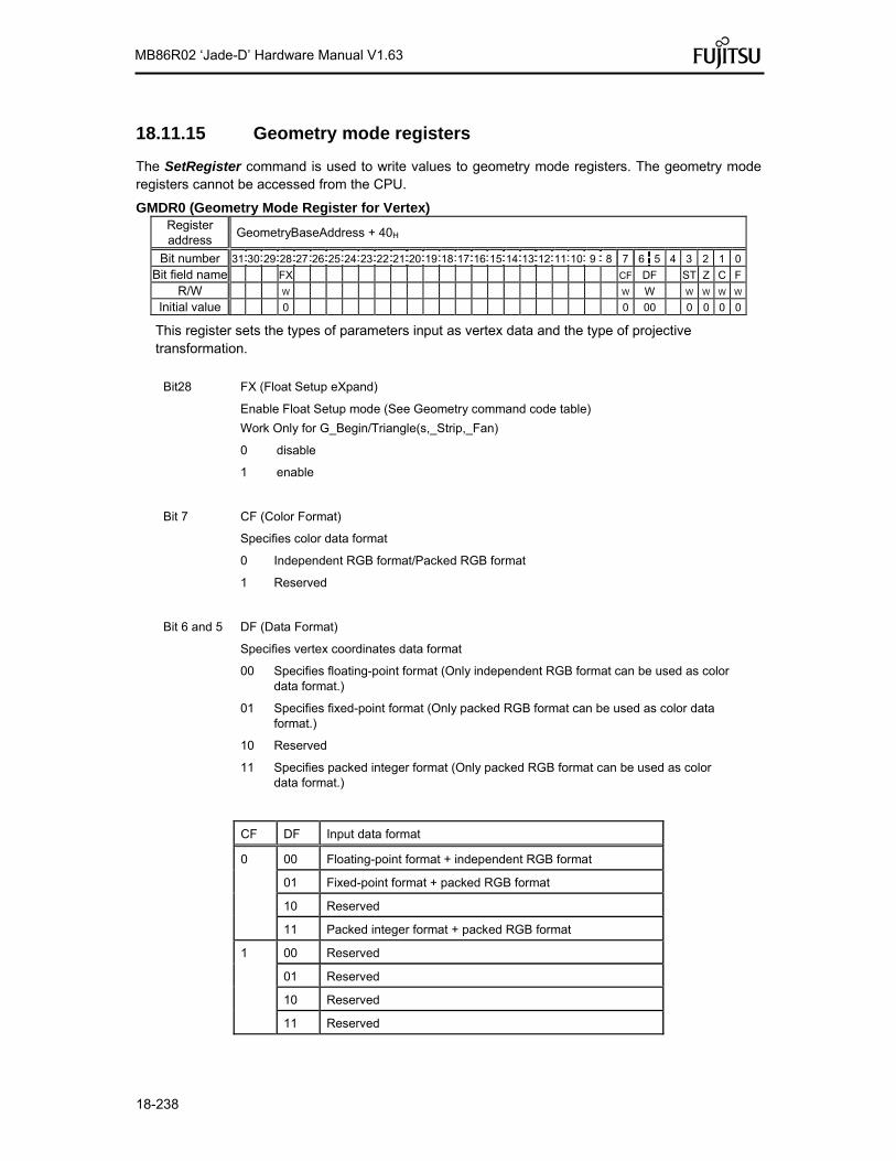
18-238
MB86R02 ‘Jade-D’ Hardware Manual V1.63
18.11.15 Geometry mode registers
The SetRegister command is used to write values to geometry mode registers. The geometry mode registers cannot be accessed from the CPU.
GMDR0 (Geometry Mode Register for Vertex) Register address
GeometryBaseAddress + 40H
Bit number 31 30 29 28 27 26 25 24 23 22 21 20 19 18 17 16 15 14 13 12 11 10 9 8 7 6 5 4 3 2 1 0
Bit field name FX CF DF ST Z C F
R/W W W W W W W W
Initial value 0 0 00 0 0 0 0
This register sets the types of parameters input as vertex data and the type of projective transformation.
Bit28 FX (Float Setup eXpand)
Enable Float Setup mode (See Geometry command code table)
Work Only for G_Begin/Triangle(s,_Strip,_Fan)
0 disable
1 enable
Bit 7 CF (Color Format)
Specifies color data format
0 Independent RGB format/Packed RGB format
1 Reserved
Bit 6 and 5 DF (Data Format)
Specifies vertex coordinates data format
00 Specifies floating-point format (Only independent RGB format can be used as color data format.)
01 Specifies fixed-point format (Only packed RGB format can be used as color data format.)
10 Reserved
11 Specifies packed integer format (Only packed RGB format can be used as color data format.)
CF DF Input data format
0 00 Floating-point format + independent RGB format
01 Fixed-point format + packed RGB format
10 Reserved
11 Packed integer format + packed RGB format
1 00 Reserved
01 Reserved
10 Reserved
11 Reserved
18-239
MB86R02 ‘Jade-D’ Hardware Manual V1.63
Bit 3 ST (texture S and T data enable)
Sets whether to use texture ST coordinates
0 Not use texture ST coordinates
1 Uses texture ST coordinates
Bit 2 Z (Z data enable)
Sets whether to use Z coordinates
0 Not use Z coordinates
1 Uses Z coordinates
Bit 1 C (Color data enable)
Sets whether to use vertex color
0 Not use vertex color
1 Uses vertex color
Bit 0 F (Frustum mode)
Sets projective transformation mode
Work only for C=0,Z=0 and ST=0 (XY only vertex) mode
0 Orthogonal projection transformation mode
1 Perspective projection transformation mode

18-240
MB86R02 ‘Jade-D’ Hardware Manual V1.63
GMDR1 (Geometry Mode Register for Line) Register address
GeometryBaseAddress + 44H
Bit number 31 30 29 28 27 26 25 24 23 22 21 20 19 18 17 16 15 14 13 12 11 10 9 8 7 6 5 4 3 2 1 0
Bit field name BO EP AA
R/W W W W
Initial value 0 0 0
This register sets the geometry mode at line drawing. This register is sharing hardware with GMDR1E, so that if GMDR1 is changed, the same bit of GMDR1E is also changed.
Bit 4 BO (Broken line Offset)
Sets broken line reference position
If you want clear initial vertex only SetRegister BLPO before G_Begin and Set 1 for this bit. (Cannot change GMDR1 within G_Begin/G_End)
0 Broken line reference position not cleared for all vertexes.
1 Broken line reference position cleared for all vertexes.
Bit 2 EP (End Point mode)
Sets end point drawing mode
Note that the end point is not drawn in line strip.
0 End point not drawn
1 End point drawn
Bit 0 AA (Anti-alias mode)
Sets anti-alias mode
0 Anti-alias not performed
1 Anti-alias performed

18-241
MB86R02 ‘Jade-D’ Hardware Manual V1.63
GMDR1E (Geometry Mode Register for Line Extension) Register address
(SetGModeRegister)
Bit number 31 30 29 28 27 26 25 24 23 22 21 20 19 18 17 16 15 14 13 12 11 10 9 8 7 6 5 4 3 2 1 0
Bit field name PO LV TC BC UW BM TM BP SP BO EP AA
R/W W W W W W W W W W W W W
Initial value 0 0 0 0 0 0 0 0 0 0 0 0
This register sets the geometry processing extended mode at line drawing.
The MB86R02 'Jade-D' extended function can be used only when the C, Z and ST fields of GMDR0 are “0”.
This register is a mirror with GMDR1, so that if GMDR1E is changed, the same bit of GMDR1 is also changed.
Bit 31 PO (Primitive Order Control)
Sets the draw order for body/edge/shadow
0 Body -> Edge -> shadow (faster)
1 Shadow -> Edge -> Body (quality for anti-alias)
Bit 30 LV (Line Version Control)
Sets the MB86R02 'Jade-D' Line algorithm version
0 Version 1.0 (for backward compatibility)
1 Version 2.0 (recommended)
Bit 20 TC (Thick line Correct)
Sets the interpolation mode for the bold line joint
0 Interpolation of bold line joint not performed
1 Interpolation of bold line joint performed
Bit 16 BC (Broken line Correct)
Sets the interpolation mode for the dashed-line pattern
0 Interpolation not performed
1 Interpolation performed using dashed-line pattern reference address fixed mode
Bit 14 UW (Uniform line Width)
Sets the line width equalization mode
0 Equalization of line width not performed
1 Equalization of line width performed
Bit 13 BM (Broken line Mode)
Sets the dashed-line pattern mode
0 Dashed-line pattern pasted vertical to principal axis of line (compatible with CREMSON).
1 Dashed-line pattern pasted vertical to theoretical line
Bit 12 TM (Thick line Mode)
Sets the bold line mode
0 Bold line drawn vertical to principal axis of line (compatible with CREMSON)

18-242
MB86R02 ‘Jade-D’ Hardware Manual V1.63
Operation is not assured when TM = 0 is used together with TC = 1, SP = 1, or BP = 1.
1 Bold line drawn vertical to theoretical line
Operation is not assured when TM = 1 is used together with BM = 0.
Bit 9 BP (Border Primitive)
Sets the drawing mode for the border primitive
0 Border primitive not drawn
1 Border primitive drawn
Bit 8 SP (Shadow Primitive)
Sets the drawing mode for the shadow primitive
0 Shadow primitive not drawn
1 Shadow primitive drawn
Bit 4 BO (Broken line Offset)
Sets the reference position of the dashed-line pattern
If you want clear initial vertex only SetRegister BLPO before G_Begin(E) and Set 1 for this bit. (Cannot change GMDR1E within G_Begin(E)/G_End(E))
0 Reference position of dashed-line pattern cleared for all vertexes
1 Reference position of dashed-line pattern not cleared for all vertexes
Bit 2 EP (End Point mode)
Sets the drawing mode for the end point
Note that the end point is always not drawn in line strip
0 End point not drawn
1 End point drawn
Bit 0 AA (Anti-alias mode)
Sets anti-alias mode
0 Anti-alias not performed
1 Anti-alias performed

18-243
MB86R02 ‘Jade-D’ Hardware Manual V1.63
GMDR2 (Geometry Mode Register for Triangle) Register address
GeometryBaseAddress + 48H
Bit number 31 30 29 28 27 26 25 24 23 22 21 20 19 18 17 16 15 14 13 12 11 10 9 8 7 6 5 4 3 2 1 0
Bit field name FD CF
R/W W W
Initial value 0 0
This register sets the geometry processing mode when a triangle is drawn.
Drawing performed using commands in range from G_Begin to G_End
Bit 2 FD (Face Definition)
Sets the face definition
0 Face defined as state with vertexes arranged clockwise
1 Face defined as state with vertexes arranged counterclockwise
Bit 0 CF (Cull Face)
Sets the drawing mode of the back
0 Back drawn
1 Back not drawn (value disabled for polygons)

18-244
MB86R02 ‘Jade-D’ Hardware Manual V1.63
GMDR2E (Geometry Mode Register for Triangle Extension) Register address
(SetGModeRegister)
Bit number 31 30 29 28 27 26 25 24 23 22 21 20 19 18 17 16 15 14 13 12 11 10 9 8 7 6 5 4 3 2 1 0
Bit field name TL SP FD CF
R/W W W W W
Initial value 0 0 0 0
This register sets the geometry processing extended mode at triangle drawing.
In case of TL=1 with texture mapping, please set perspective correction.
Non-top-left-part’s pixel quality is less than body. (using approximate calculation)
Bit 10 TL (Top-Left rule mode)
Sets the drawing algorithm
0 Top-left rule applied (compatible with CREMSON)
1 Top-left rule not applied
Bit 8 SP (Shadow Primitive)
Sets the drawing mode for the shadow primitive
0 Shadow primitive not drawn
1 Shadow primitive drawn
Bit 2 FD (Face Definition)
Sets the face definition
0 Face defined as state with vertexes arranged clockwise
1 Face defined as state with vertexes arranged counterclockwise
Bit 0 CF (Cull Face)
Sets the drawing mode of the back
0 Back drawn
1 Back not drawn (value disabled for polygons)

18-245
MB86R02 ‘Jade-D’ Hardware Manual V1.63
18.11.16 Display list FIFO registers
DFIFOG (Geometry Displaylist FIFO with Geometry) Register address
Geometry BaseAddress + 400H
Bit number 31 30 29 28 27 26 25 24 23 22 21 20 19 18 17 16 15 14 13 12 11 10 9 8 7 6 5 4 3 2 1 0
Bit field name DFIFOG
R/W W
Initial value Don’t care
FIFO registers for Display List transfer

18-246
MB86R02 ‘Jade-D’ Hardware Manual V1.63
18.11.17 Display List DMA contol registers
18.11.17.1 Display List DMA contol register list
BaseAddress = HostBaseAddress (=0xF1FC_0000)
Address 31 30 29 28 27 26 25 24 23 22 21 20 19 18 17 16 15 14 13 12 11 10 9 8 7 6 5 4 3 2 1 0
FIFC
0008
LTS
LTS
DT
S
FIFC
0010
LSTA
LST
A
FIFC
0040
LSA
LSA
FIFC
0044
LCO
LCO
FIFC
0048
LREQ
LRE
Q

18-247
MB86R02 ‘Jade-D’ Hardware Manual V1.63
LTS (display Transfer Stop) Register address
HostBaseAddress + 09H
Bit number 7 6 5 4 3 2 1 0
Bit field name Reserved LTS
R/W R0 RW
Initial value 0 0
This register suspends DisplayList transfer.
Ongoing DisplayList transfer is suspended by setting LTS to “1”.
LSTA (displayList transfer STAtus) Register address
HostBaseAddress + 10H
Bit number 7 6 5 4 3 2 1 0
Bit field name Reserved LSTA
R/W R0 R
Initial value 0 0
This register indicates the DisplayList transfer status from Graphics Memory. LSTA is set to “1” while DisplayList transfer is in progress. This status is cleared to 0 when DisplayList transfer is completed

18-248
MB86R02 ‘Jade-D’ Hardware Manual V1.63
LSA (displayList Source Address) Register address
HostBaseAddress + 40H
Bit number 31 30 29 28 27 26 25 24 23 22 21 20 19 18 17 16 15 14 13 12 11 10 9 8 7 6 5 4 3 2 1 0
Bit field name Reserved LSA
R/W R0 RW R0
Initial value 0 Don’t care 0
This register sets the DisplayList transfer source address. When DisplayList is transferred from Graphics Memory, set the transfer start address of DisplayList stored in Graphics Memory. Since the lower two bits of this register are always treated as “0”, DisplayList must be 4-byte aligned. The values set at this register do not change during or after transfer.
LCO (displayList Count) Register address
HostBaseAddress + 44H
Bit number 31 30 29 28 27 26 25 24 23 22 21 20 19 18 17 16 15 14 13 12 11 10 9 8 7 6 5 4 3 2 1 0
Bit field name Reserved LCO
R/W R0 RW
Initial value 0 Don’t care
This register sets the DisplayList transfer count. Set the display list transfer count by the long word. When “1h” is set, 1-word data is transferred. When “0” is set, it is considered to be the maximum count and 16M (16,777,216) words of data are transferred. The values set at this register do not change during or after transfer.
LREQ (displayList transfer REQuest) Register address
HostBaseAddress + 48H
Bit number 7 6 5 4 3 2 1 0
Bit field name Reserved LREQ
R/W R0 RW1
Initial value 0 0
This register triggers DisplayList transfer from the Graphics Memory. Transfer is started by setting LREQ to “1”. The DisplayList is transferred from the Graphics Memory to the internal display list FIFO. Access to the display list FIFO by the CPU or DMA is disabled during transfer.

18-249
MB86R02 ‘Jade-D’ Hardware Manual V1.63
18.11.18 Interrupt registers
18.11.18.1 Interrupt register list
BaseAddress = HostBaseAddress (=0xF1FC_0000)
Address 31 30 29 28 27 26 25 24 23 22 21 20 19 18 17 16 15 14 13 12 11 10 9 8 7 6 5 4 3 2 1 0
FIFC
0020
IST
IST
FIFC
0024
IMASK
IMASK
IST (Interrupt STatus) Register address
HostBaseAddress + 20H
Bit number 31 30 29 28 27 26 25 24 23 22 21 20 19 18 17 16 15 14 13 12 11 10 9 8 7 6 5 4 3 2 1 0
Bit field name Reserved Resv Reserved IST
R/W R0 R0W0 R0 RW0
Initial value 0 0 0 0
*1 Reserved
This register indicates the current interrupt status. It shows that an interrupt request is issued when “1” is set to this register. The interrupt status is cleared by writing “0” to this register.
Bit 0 CERR (Command Error Flag)
Indicates drawing command execution error interrupt
Bit 1 CEND (Command END)
Indicates drawing command end interrupt
Bit 2 VSYNC0 (Vertical Sync. of display 0)
Indicates vertical interrupt synchronization
Bit 3 FSYNC0 (Frame Sync. of display 0)
Indicates frame synchronization interrupt
Bit 4 SYNCERR0 (Sync. Error of display 0)
Indicates external synchronization error interrupt
Bit 5 REGUD0 (Register update of display 0)
Indicates register update interrupt
Bit 6 VSYNC1 (Vertical Sync. of display 1)
Indicates vertical interrupt synchronization
Bit 7 FSYNC1 (Frame Sync. of display 1)
Indicates frame synchronization interrupt
Bit 8 SYNCERR1 (Sync. Error of display 1)
Indicates external synchronization error interrupt
Bit 9 REGUD1 (Register update of display 1)
Indicates register update interrupt

18-250
MB86R02 ‘Jade-D’ Hardware Manual V1.63
Bit 10 CAP0 (Capture 0)
Indicates video capture 0 interrupt
Bit 11 CAP1 (Capture 1)
Indicates video capture 1 interrupt
Bit 17 and 16 Reserved
This field is provided for testing.
Normally, the read value is “0”, but note that it may be “1” when a drawing command error (Bit 0) has occurred.
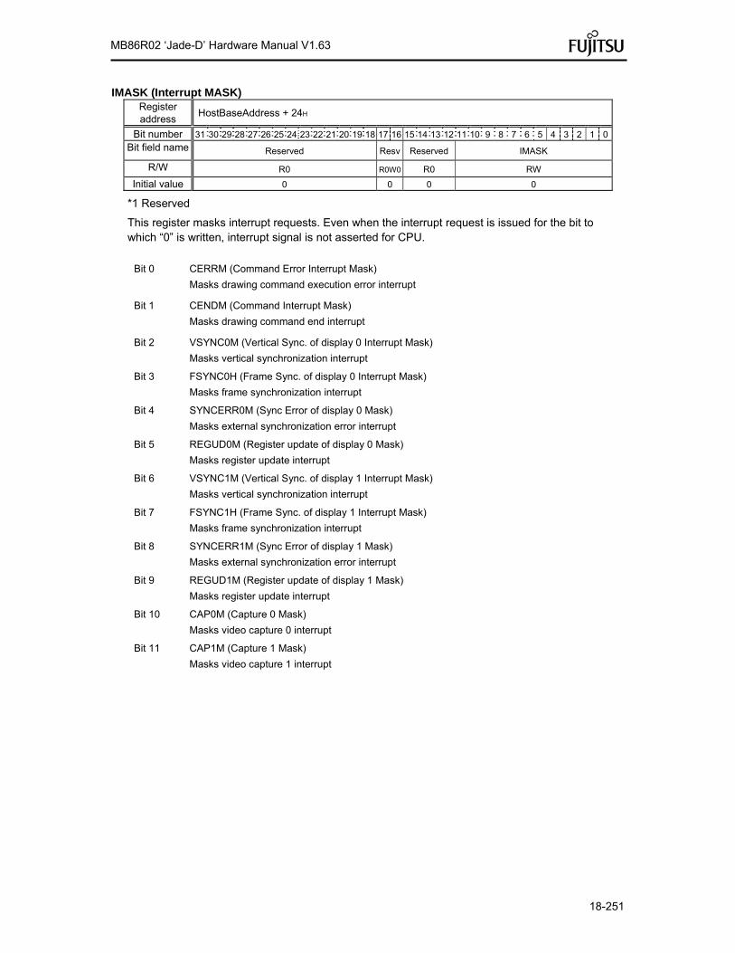
18-251
MB86R02 ‘Jade-D’ Hardware Manual V1.63
IMASK (Interrupt MASK) Register address
HostBaseAddress + 24H
Bit number 31 30 29 28 27 26 25 24 23 22 21 20 19 18 17 16 15 14 13 12 11 10 9 8 7 6 5 4 3 2 1 0
Bit field name Reserved Resv Reserved IMASK
R/W R0 R0W0 R0 RW
Initial value 0 0 0 0
*1 Reserved
This register masks interrupt requests. Even when the interrupt request is issued for the bit to which “0” is written, interrupt signal is not asserted for CPU.
Bit 0 CERRM (Command Error Interrupt Mask)
Masks drawing command execution error interrupt
Bit 1 CENDM (Command Interrupt Mask)
Masks drawing command end interrupt
Bit 2 VSYNC0M (Vertical Sync. of display 0 Interrupt Mask)
Masks vertical synchronization interrupt
Bit 3 FSYNC0H (Frame Sync. of display 0 Interrupt Mask)
Masks frame synchronization interrupt
Bit 4 SYNCERR0M (Sync Error of display 0 Mask)
Masks external synchronization error interrupt
Bit 5 REGUD0M (Register update of display 0 Mask)
Masks register update interrupt
Bit 6 VSYNC1M (Vertical Sync. of display 1 Interrupt Mask)
Masks vertical synchronization interrupt
Bit 7 FSYNC1H (Frame Sync. of display 1 Interrupt Mask)
Masks frame synchronization interrupt
Bit 8 SYNCERR1M (Sync Error of display 1 Mask)
Masks external synchronization error interrupt
Bit 9 REGUD1M (Register update of display 1 Mask)
Masks register update interrupt
Bit 10 CAP0M (Capture 0 Mask)
Masks video capture 0 interrupt
Bit 11 CAP1M (Capture 1 Mask)
Masks video capture 1 interrupt

MB86R02 ‘Jade-D’ Hardware Manual V1.63
19-1
19 Color Lookup Table (CLUT)
19.1 Color LUT
19.1.1 Overview A Color LUT (CLUT) is used either to compensate the non-linearity of color transmission or to adapt to the individual characteristics of a display panel by converting the logical color to a physical color that can be displayed on a monitor. The CLUT is simply a block of fast RAM with 256 entries, each of which is 10 bits wide for each RGB component and can be programmed in parallel by software. The 256 entries are directly mapped to the ColourIndex register address space. Additionally, the red colour channel can be used on all three colour lookup tables to translate index values to colours.
19.1.2 Features The contents of the CLUT are generated i.g by the function y=x power k, where k is dependant on the panel characteristics. The CLUT is a part of the display output interface and must be initialized by the application software during the initialization phase because there are no default values for its contents. • Single block table with 256 entries and 10 bit accuracy for each color with optional index mode • Parallel programming of the table content • Direct mapping to Configuration Address space • Bypass
G (8bit)
B( 8bit)
LUT256x1024
R (8bit) R’ (10bit)
G’ (10bit)
B’ (10bit)
Figure 19-1 LUT Organization
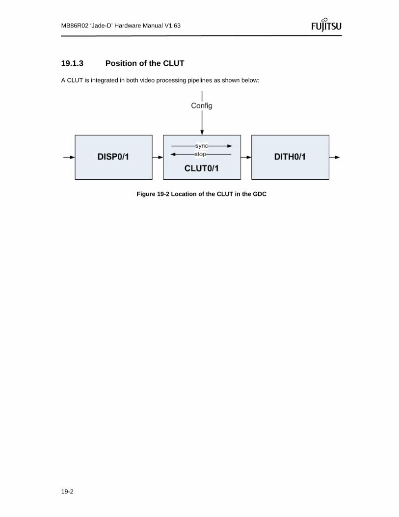
MB86R02 ‘Jade-D’ Hardware Manual V1.63
19-2
19.1.3 Position of the CLUT A CLUT is integrated in both video processing pipelines as shown below:
Figure 19-2 Location of the CLUT in the GDC

MB86R02 ‘Jade-D’ Hardware Manual V1.63
19-3
19.2 Software Interface
19.2.1 Format of Register Description The register descriptions in the following sections use the format shown below to describe each bit field of a register. Register address Offset
Bit number 31 30 29 28 27 26 25 24 23 22 21 20 19 18 17 16 15 14 13 12 11 10 9 8 7 6 5 4 3 2 1 0
Field name
R/W
Reset value
Meaning of items and sign Register address
Register address shows the address (Offset address) of the register. Bit number
Bit number shows bit position of the register. Field name
Field name shows bit name of the register. R/W
R/W shows the read/write attribute of each bit field: R: Read W: Write W1C: Writing a value of "1" clears the register.
Reset value Reset value indicates the value of each bit field immediately after reset. 0: Initial value is "0". 1: Initial value is "1". X: Undefined.
Unused register fields are marked with a solid grey background. Bit vectors are unsigned integers, if nothing else specified.
19.2.2 Global Address For module base address refer to inter-module specification or global address map of the respective LSI.
19.2.3 Register Summary
Address Register Name DescriptionBase address + 0H
: Base address + 3FFH
ColourIndex Lookuptable for colour indexing
Base address + 400H CLUTControl Colour Lookuptable Control
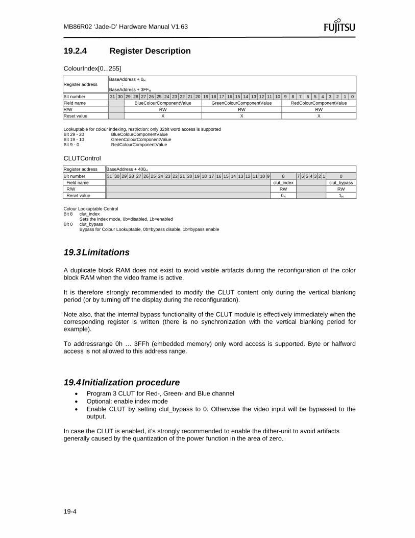
MB86R02 ‘Jade-D’ Hardware Manual V1.63
19-4
19.2.4 Register Description ColourIndex[0...255]
Register address BaseAddress + 0H : BaseAddress + 3FFH
Bit number 31 30 29 28 27 26 25 24 23 22 21 20 19 18 17 16 15 14 13 12 11 10 9 8 7 6 5 4 3 2 1 0
Field name BlueColourComponentValue GreenColourComponentValue RedColourComponentValue
R/W RW RW RW
Reset value X X X
Lookuptable for colour indexing, restriction: only 32bit word access is supported Bit 29 - 20 BlueColourComponentValue Bit 19 - 10 GreenColourComponentValue Bit 9 - 0 RedColourComponentValue
CLUTControl
Register address BaseAddress + 400H
Bit number 31 30 29 28 27 26 25 24 23 22 21 20 19 18 17 16 15 14 13 12 11 10 9 8 7 6 5 4 3 2 1 0
Field name clut_index clut_bypass
R/W RW RW
Reset value 0H 1H
Colour Lookuptable Control Bit 8 clut_index
Sets the index mode, 0b=disabled, 1b=enabled Bit 0 clut_bypass
Bypass for Colour Lookuptable, 0b=bypass disable, 1b=bypass enable
19.3 Limitations A duplicate block RAM does not exist to avoid visible artifacts during the reconfiguration of the color block RAM when the video frame is active. It is therefore strongly recommended to modify the CLUT content only during the vertical blanking period (or by turning off the display during the reconfiguration). Note also, that the internal bypass functionality of the CLUT module is effectively immediately when the corresponding register is written (there is no synchronization with the vertical blanking period for example). To addressrange 0h … 3FFh (embedded memory) only word access is supported. Byte or halfword access is not allowed to this address range.
19.4 Initialization procedure Program 3 CLUT for Red-, Green- and Blue channel Optional: enable index mode Enable CLUT by setting clut_bypass to 0. Otherwise the video input will be bypassed to the
output. In case the CLUT is enabled, it’s strongly recommended to enable the dither-unit to avoid artifacts generally caused by the quantization of the power function in the area of zero.

20-1
MB86R02 ‘Jade-D’ Hardware Manual V1.63
20 Dither Unit
20.1 Overview
A dither unit is required in a display processing pipe line to display images on a graphic device which has less color levels than those contained in the original picture data in order to obtain a better visual result. To achieve this, the dither unit modifies pixels in such a way that the average color level of these pixels is used.
Figure 20-1 DITH inputs/outputs
20.1.1 Features
The dither unit supports: • Bypass mode
In bypass mode, the input data will be passed to the output, where the 2 LSB of the input data will be dropped.
• Spatial dithering mode
In spatial dithering mode, the intensities of neighboring pixels are modified so that their combined intensities average out to the desired value. Using a 4x4 matrix (see table 1.1.1), the incoming pixel value will be filtered depending on the location of the pixel in a frame. The pixel location is generated according to the horizontal and vertical synchronization signals.
0 8 2 10 12 4 14 6 3 11 1 9
15 7 13 5 Table 1.1.1 : 4x4 Ordered dither matrix

20-2
MB86R02 ‘Jade-D’ Hardware Manual V1.63
• Temporal dithering mode
In temporal dithering mode, the temporal variation of the pixels can be achieved by generating a random vector that is used for addressing the dither matrix.
• Output resolution of 888 / 777 / 666 / 565 (see table 1.1.2) • Align the output data to the upper or lower part of the byte in order to display the output pixels on an RGB888 monitor (see table 1.1.2)
dither_ Align
dither_ format
Output format 888/777/666/565
Bit7 Bit6 Bit5 Bit4 Bit3 Bit2 Bit1 Bit0 X 888 RGB 888 0 777 0 RGB 777 1 777 RGB 777 0 0 666 0 0 RGB 666 1 666 RGB 666 0 0
0 565 0 0 0 R5 0 0 G6 0 0 0 B5
1 565 R5 0 0 0
G6 0 0 B5 0 0 0
Table 1.1.2: Output format as a function of dither_align and dither_format
20.1.2 Position
One dither unit is integrated in each video processing pipe. In MB86R02 (Jade-D), the dither unit is used to adapt to the individual characteristics of the display panel.
Figure 20-2 Location of the DITH unit in the GDC

20-3
MB86R02 ‘Jade-D’ Hardware Manual V1.63
20.1.3 Timing chart
Figure 20-3 Timing diagram for spatial dithering mode

20-4
MB86R02 ‘Jade-D’ Hardware Manual V1.63
20.2 Software Interface
20.2.1 Format of Register Description The register descriptions in the following sections use the format shown below to describe each bit field of a register. Register address Offset
Bit number 31 30 29 28 27 26 25 24 23 22 21 20 19 18 17 16 15 14 13 12 11 10 9 8 7 6 5 4 3 2 1 0
Field name
R/W
Reset value
Meaning of items and sign Register address
Register address shows the address (Offset address) of the register. Bit number
Bit number shows bit position of the register. Field name
Field name shows bit name of the register. R/W
R/W shows the read/write attribute of each bit field: R: Read W: Write W1C: Writing a value of "1" clears the register.
Reset value Reset value indicates the value of each bit field immediately after reset. 0: Initial value is "0". 1: Initial value is "1". X: Undefined.
Unused register fields are marked with a solid grey background. Bit vectors are unsigned integers, if nothing else specified.
20.2.2 Global Address For module base address refer to inter-module specification or global address map of the respective LSI.
20.2.3 Register Summary
Address Register Name DescriptionBase address + 0H DitherControl Dither Unit Control
20.2.4 Register Description DitherControl
Register address BaseAddress + 0H
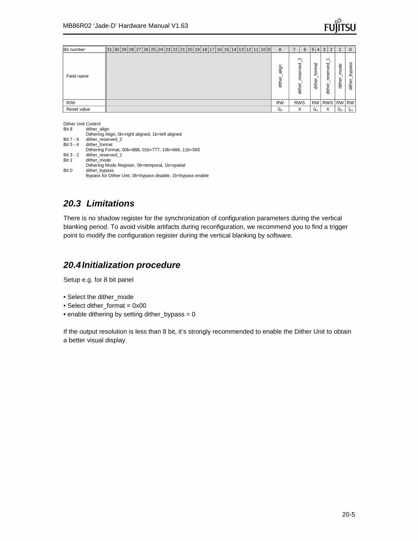
20-5
MB86R02 ‘Jade-D’ Hardware Manual V1.63
Bit number 31 30 29 28 27 26 25 24 23 22 21 20 19 18 17 16 15 14 13 12 11 10 9 8 7 6 5 4 3 2 1 0
Field name
dith
er_
alig
n
dith
er_
rese
rve
d_2
dith
er_f
orm
at
dith
er_
rese
rve
d_1
dith
er_m
ode
dith
er_b
ypas
s
R/W RW RWS RW RWS RW RW
Reset value 0H X 0H X 0H 1H
Dither Unit Control Bit 8 dither_align
Dithering Align, 0b=right aligned, 1b=left aligned Bit 7 - 6 dither_reserved_2 Bit 5 - 4 dither_format
Dithering Format, 00b=888, 01b=777, 10b=666, 11b=565 Bit 3 - 2 dither_reserved_1 Bit 1 dither_mode
Dithering Mode Register, 0b=temporal, 1b=spatial Bit 0 dither_bypass
Bypass for Dither Unit, 0b=bypass disable, 1b=bypass enable
20.3 Limitations
There is no shadow register for the synchronization of configuration parameters during the vertical blanking period. To avoid visible artifacts during reconfiguration, we recommend you to find a trigger point to modify the configuration register during the vertical blanking by software.
20.4 Initialization procedure
Setup e.g. for 8 bit panel • Select the dither_mode • Select dither_format = 0x00 • enable dithering by setting dither_bypass = 0 If the output resolution is less than 8 bit, it’s strongly recommended to enable the Dither Unit to obtain a better visual display.

MB86R02 ‘Jade-D’ Hardware Manual V1.63
21-1
21 Signature Generator (SIG)
21.1 Position of Block in whole LSI
Figure 21-1 Location of the SIG unit in the GDC
21.2 Overview The Signature Generator unit (SIG) calculates different types of checksums for input data. Application is the generation of a checksum (signature) for pixel stream data for a user-defined evaluation window (whose size and position can be programmed). The system micro controller can use such signatures e.g. to determine whether the displayed image is exactly identical (or almost identical) to the original image data submitted. This is necessary for critical safety displays and helps to fulfil the requirements of safety standards (e.g. Automotive Safety Integrity Level ASIL).
21.3 Feature List
Generation of 2 different picture signatures for each color channel - summation of color values - CRC-32 for color values
Programmable evaluation window position and size Programmable evaluation window mask Automatic monitoring using reference signature registers Interrupt generation Programmable picture source Self restoring error counter

MB86R02 ‘Jade-D’ Hardware Manual V1.63
21-2
21.3.1 Signature A: CRC-32 Signature Standard CRC-32 as in the Ethernet Standard (CRC-32-IEEE 802.3) is calculated for each color channel in the evaluation window area. The default polynome is: x32 + x26 + x23 + x22 + x16 + x12 + x11 + x10 + x8 + x7 + x5 + x4 + x2 + x + 1 Start value: FFFF_FFFF
21.3.2 Signature B: Summation Signature The sum of pixel color values for each color channel (R, G, B) in the evaluation window area is calculated.
21.3.3 Programmable Evaluation Window (Position and Size) Position and size of the evaluation window are programmable.
21.3.4 Programmable Evaluation Window Mask A programmable mask window allows the exclusion of incoming pixels for the signature calculation.
21.3.5 Automatic Monitoring and Interrupt A set of reference signature registers allows the monitoring of the calculated signatures. An interrupt can be generated on the detection of a difference between the calculated signature and the reference value. For signature B the difference can be threshold filtered to limit the interrupt load for the microcontroller.
21.3.6 Self Restoring Error Counter A counter is incremented if one of the active signature results differs from the corresponding reference values. If a programmable error counter threshold is reached an interrupt may be generated The same counter is reset to zero if a programmable number of consecutive video frames with correct signature values is received.
21.3.7 Interrupts For Control Flow An interrupt can be generated for both the start and end of a signature calculation. The start interrupt (CfgCop) indicates that the configuration parameters (e.g. window coordinates) have been copied from the shadow registers and are now active for the current signature calculation. This allows that next configuration parameters can be loaded into the (shadow) registers without disturbing the current calculation. The end interrupt (ResVal) indicates a signature calculation has completed and the result data can be read from the result shadow registers. These interrupts help to control signature calculations for every incoming frame with different evaluation window coordinates.
21.3.8 Programmable Input Picture Source Input data can be selected from four different sources. Four different sources can be connected on LSI top level.

MB86R02 ‘Jade-D’ Hardware Manual V1.63
21-3
21.3.9 Limitations
Maximum Resolution for picture sources and windows is 4096 x 4096
Evaluation window position must be completely inside the picture source frame
Source Select must be configured before evaluation window coordinates and can not be
changed during operation.
No support for interlaced sources. Also for de-interlaced sources no special processing is supported, that means reference values must be calculated by SW considering the right de-interlace algorithm for such material.
Limitation of SW control flow for cyclic monitoring of changing evaluation windows, see
chapter 21.6.5
21.4 Software Interface
21.4.1 Format of Register Description The register descriptions in the following sections use the format shown below to describe each bit field of a register. Register address Offset
Bit number 31 30 29 28 27 26 25 24 23 22 21 20 19 18 17 16 15 14 13 12 11 10 9 8 7 6 5 4 3 2 1 0
Field name
R/W
Reset value
Meaning of items and sign Register address
Register address shows the address (Offset address) of the register. Bit number
Bit number shows bit position of the register. Field name
Field name shows bit name of the register. R/W
R/W shows the read/write attribute of each bit field: R: Read W: Write W1C: Writing a value of "1" clears the register.
Reset value Reset value indicates the value of each bit field immediately after reset. 0: Initial value is "0". 1: Initial value is "1". X: Undefined.
Unused register fields are marked with a solid grey background. Bit vectors are unsigned integers, if nothing else specified.
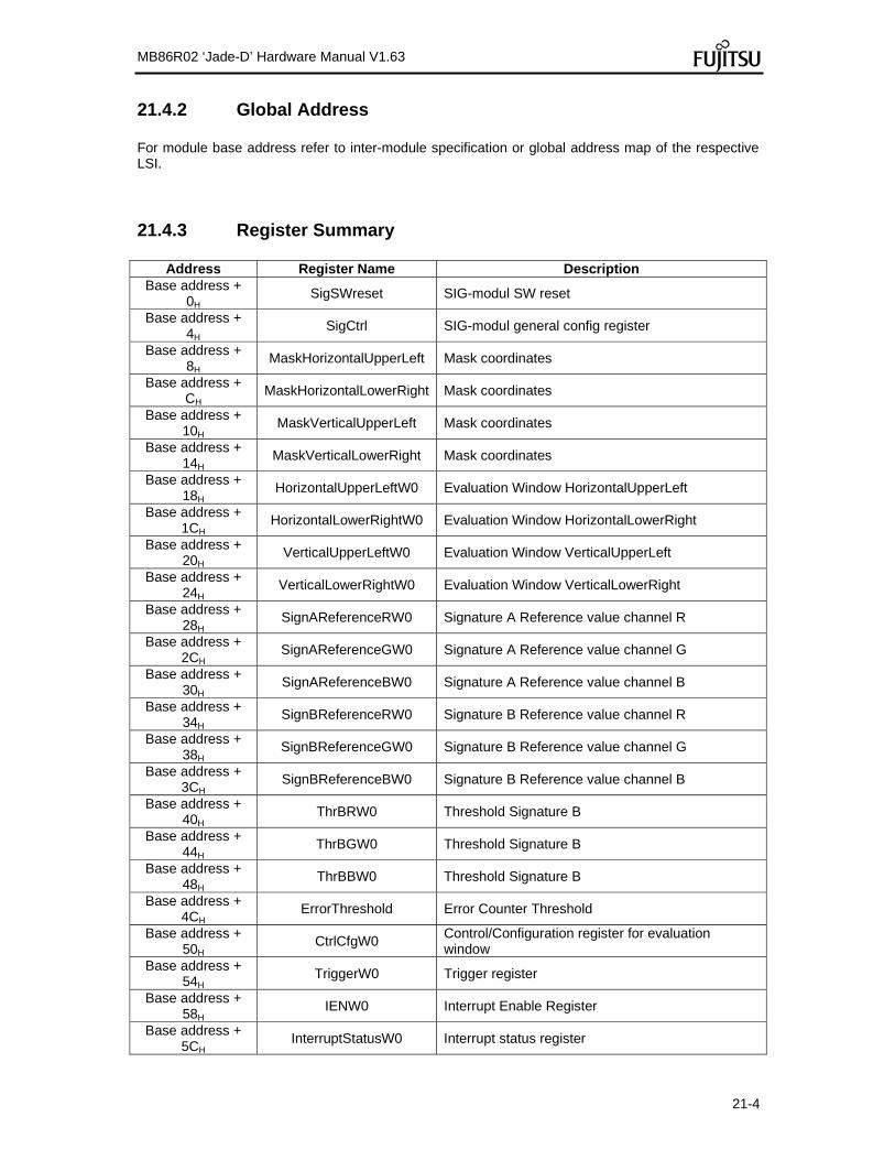
MB86R02 ‘Jade-D’ Hardware Manual V1.63
21-4
21.4.2 Global Address For module base address refer to inter-module specification or global address map of the respective LSI.
21.4.3 Register Summary
Address Register Name Description Base address +
0H SigSWreset SIG-modul SW reset
Base address + 4H
SigCtrl SIG-modul general config register
Base address + 8H
MaskHorizontalUpperLeft Mask coordinates
Base address + CH
MaskHorizontalLowerRight Mask coordinates
Base address + 10H
MaskVerticalUpperLeft Mask coordinates
Base address + 14H
MaskVerticalLowerRight Mask coordinates
Base address + 18H
HorizontalUpperLeftW0 Evaluation Window HorizontalUpperLeft
Base address + 1CH
HorizontalLowerRightW0 Evaluation Window HorizontalLowerRight
Base address + 20H
VerticalUpperLeftW0 Evaluation Window VerticalUpperLeft
Base address + 24H
VerticalLowerRightW0 Evaluation Window VerticalLowerRight
Base address + 28H
SignAReferenceRW0 Signature A Reference value channel R
Base address + 2CH
SignAReferenceGW0 Signature A Reference value channel G
Base address + 30H
SignAReferenceBW0 Signature A Reference value channel B
Base address + 34H
SignBReferenceRW0 Signature B Reference value channel R
Base address + 38H
SignBReferenceGW0 Signature B Reference value channel G
Base address + 3CH
SignBReferenceBW0 Signature B Reference value channel B
Base address + 40H
ThrBRW0 Threshold Signature B
Base address + 44H
ThrBGW0 Threshold Signature B
Base address + 48H
ThrBBW0 Threshold Signature B
Base address + 4CH
ErrorThreshold Error Counter Threshold
Base address + 50H
CtrlCfgW0 Control/Configuration register for evaluation window
Base address + 54H
TriggerW0 Trigger register
Base address + 58H
IENW0 Interrupt Enable Register
Base address + 5CH
InterruptStatusW0 Interrupt status register

MB86R02 ‘Jade-D’ Hardware Manual V1.63
21-5
Base address + 60H
StatusW0 status register
Base address + 64H
Signature_error The amount of video frames with signature errors
Base address + 68H
SignatureARW0 Signature A Result channel R
Base address + 6CH
SignatureAGW0 Signature A Result channel G
Base address + 70H
SignatureABW0 Signature A Result channel B
Base address + 74H
SignatureBRW0 Signature B Result channel R
Base address + 78H
SignatureBGW0 Signature B Result channel G
Base address + 7CH
SignatureBBW0 Signature B Result channel B
21.4.4 Register Description SigSWreset
Register address BaseAddress + 0H
Bit number 31 30 29 28 27 26 25 24 23 22 21 20 19 18 17 16 15 14 13 12 11 10 9 8 7 6 5 4 3 2 1 0
Field name SWRes
R/W RW
Reset value 0H
SIG-modul SW reset Bit 0 SWRes
SW reset
SigCtrl
Register address BaseAddress + 4H
Bit number 31 30 29 28 27 26 25 24 23 22 21 20 19 18 17 16 15 14 13 12 11 10 9 8 7 6 5 4 3 2 1 0
Field name SrcSel Vmask_mode Hmask_mode
R/W RW RW RW
Reset value 0H 0H 0H
SIG-modul general config register Bit 17 - 16 SrcSel
Source Select 00b=source 0, 01b=source 1, 10b=source 2, 11b=source 3 Bit 9 - 8 Vmask_mode
00b=nomask, 01b=mask inside vertical coordinates, 10b=mask outside vertical coordinates, 11b=reserved Bit 1 - 0 Hmask_mode
00b=nomask, 01b=mask inside horizontal coordinates, 10b=mask outside horizontal coordinates, 11b=reserved
MaskHorizontalUpperLeft
Register address BaseAddress + 8H
Bit number 31 30 29 28 27 26 25 24 23 22 21 20 19 18 17 16 15 14 13 12 11 10 9 8 7 6 5 4 3 2 1 0
Field name MaskHorizontalUpperLeft
R/W RW
Reset value 0H
Mask coordinates Bit 11 - 0 MaskHorizontalUpperLeft
Mask Horizontal Upper Left
MaskHorizontalLowerRight
Register address BaseAddress + CH
Bit number 31 30 29 28 27 26 25 24 23 22 21 20 19 18 17 16 15 14 13 12 11 10 9 8 7 6 5 4 3 2 1 0
Field name MaskHorizontalLowerRight
R/W RW

MB86R02 ‘Jade-D’ Hardware Manual V1.63
21-6
Reset value 0H
Mask coordinates Bit 11 - 0 MaskHorizontalLowerRight
Mask Horizontal Lower right
MaskVerticalUpperLeft
Register address BaseAddress + 10H
Bit number 31 30 29 28 27 26 25 24 23 22 21 20 19 18 17 16 15 14 13 12 11 10 9 8 7 6 5 4 3 2 1 0
Field name MaskVerticalUpperLeft
R/W RW
Reset value 0H
Mask coordinates Bit 11 - 0 MaskVerticalUpperLeft
Mask Vertical Upper Left
MaskVerticalLowerRight
Register address BaseAddress + 14H
Bit number 31 30 29 28 27 26 25 24 23 22 21 20 19 18 17 16 15 14 13 12 11 10 9 8 7 6 5 4 3 2 1 0
Field name MaskVerticalLowerRight
R/W RW
Reset value 0H
Mask coordinates Bit 11 - 0 MaskVerticalLowerRight
Mask Vertical Lower Right
HorizontalUpperLeftW0
Register address BaseAddress + 18H
Bit number 31 30 29 28 27 26 25 24 23 22 21 20 19 18 17 16 15 14 13 12 11 10 9 8 7 6 5 4 3 2 1 0
Field name HorizontalUpperLeftW0
R/W RW
Reset value 0H
Evaluation Window HorizontalUpperLeft Bit 11 - 0 HorizontalUpperLeftW0
Evaluation Window HorizontalUpperLeft , Register content is overtaken with write of Register TriggerW0.Trigger
HorizontalLowerRightW0
Register address BaseAddress + 1CH
Bit number 31 30 29 28 27 26 25 24 23 22 21 20 19 18 17 16 15 14 13 12 11 10 9 8 7 6 5 4 3 2 1 0
Field name HorizontalLowerRightW0
R/W RW
Reset value 0H
Evaluation Window HorizontalLowerRight Bit 11 - 0 HorizontalLowerRightW0
Evaluation Window HorizontalLowerRight, Register content is overtaken with write of Register TriggerW0.Trigger
VerticalUpperLeftW0
Register address BaseAddress + 20H
Bit number 31 30 29 28 27 26 25 24 23 22 21 20 19 18 17 16 15 14 13 12 11 10 9 8 7 6 5 4 3 2 1 0
Field name VerticalUpperLeftW0
R/W RW
Reset value 0H
Evaluation Window VerticalUpperLeft Bit 11 - 0 VerticalUpperLeftW0
Evaluation Window VerticalUpperLeft, Register content is overtaken with write of Register TriggerW0.Trigger
VerticalLowerRightW0
Register address BaseAddress + 24H
Bit number 31 30 29 28 27 26 25 24 23 22 21 20 19 18 17 16 15 14 13 12 11 10 9 8 7 6 5 4 3 2 1 0
Field name VerticalLowerRightW0

MB86R02 ‘Jade-D’ Hardware Manual V1.63
21-7
R/W RW
Reset value 0H
Evaluation Window VerticalLowerRight Bit 11 - 0 VerticalLowerRightW0
Evaluation Window VerticalLowerRight , Register content is overtaken with write of Register TriggerW0.Trigger
SignAReferenceRW0
Register address BaseAddress + 28H
Bit number 31 30 29 28 27 26 25 24 23 22 21 20 19 18 17 16 15 14 13 12 11 10 9 8 7 6 5 4 3 2 1 0
Field name SignAReferenceRW0
R/W RW
Reset value 0H
Signature A Reference value channel R Bit 31 - 0
SignAReferenceRW0 Signature A Reference value channel R, Register content is overtaken with write of Register TriggerW0.Trigger, during cyclic mode with every frame start
SignAReferenceGW0
Register address BaseAddress + 2CH
Bit number 31 30 29 28 27 26 25 24 23 22 21 20 19 18 17 16 15 14 13 12 11 10 9 8 7 6 5 4 3 2 1 0
Field name SignAReferenceGW0
R/W RW
Reset value 0H
Signature A Reference value channel G Bit 31 - 0
SignAReferenceGW0 Signature A Reference value channel G, Register content is overtaken with write of Register TriggerW0.Trigger, during cyclic mode with every frame start
SignAReferenceBW0
Register address BaseAddress + 30H
Bit number 31 30 29 28 27 26 25 24 23 22 21 20 19 18 17 16 15 14 13 12 11 10 9 8 7 6 5 4 3 2 1 0
Field name SignAReferenceBW0
R/W RW
Reset value 0H
Signature A Reference value channel B Bit 31 - 0
SignAReferenceBW0 Signature A Reference value channel B, Register content is overtaken with write of Register TriggerW0.Trigger, during cyclic mode with every frame start
SignBReferenceRW0
Register address BaseAddress + 34H
Bit number 31 30 29 28 27 26 25 24 23 22 21 20 19 18 17 16 15 14 13 12 11 10 9 8 7 6 5 4 3 2 1 0
Field name SignBReferenceRW0
R/W RW
Reset value 0H
Signature B Reference value channel R Bit 31 - 0
SignBReferenceRW0 Signature B Reference value channel R, Register content is overtaken with write of Register TriggerW0.Trigger, during cyclic mode with every frame start
SignBReferenceGW0
Register address BaseAddress + 38H
Bit number 31 30 29 28 27 26 25 24 23 22 21 20 19 18 17 16 15 14 13 12 11 10 9 8 7 6 5 4 3 2 1 0
Field name SignBReferenceGW0
R/W RW
Reset value 0H
Signature B Reference value channel G Bit 31 - 0
SignBReferenceGW0 Signature B Reference value channel G, Register content is overtaken with write of Register TriggerW0.Trigger, during cyclic mode with every frame start

MB86R02 ‘Jade-D’ Hardware Manual V1.63
21-8
SignBReferenceBW0
Register address BaseAddress + 3CH
Bit number 31 30 29 28 27 26 25 24 23 22 21 20 19 18 17 16 15 14 13 12 11 10 9 8 7 6 5 4 3 2 1 0
Field name SignBReferenceBW0
R/W RW
Reset value 0H
Signature B Reference value channel B Bit 31 - 0
SignBReferenceBW0 Signature B Reference value channel B, Register content is overtaken with write of Register TriggerW0.Trigger, during cyclic mode with every frame start
ThrBRW0
Register address BaseAddress + 40H
Bit number 31 30 29 28 27 26 25 24 23 22 21 20 19 18 17 16 15 14 13 12 11 10 9 8 7 6 5 4 3 2 1 0
Field name ThrBRW0
R/W RW
Reset value 0H
Threshold Signature B Bit 31 - 0
ThrBRW0 Threshold Signature B for channels R, Register content is overtaken with write of Register TriggerW0.Trigger, during cyclic mode with every frame start
ThrBGW0
Register address BaseAddress + 44H
Bit number 31 30 29 28 27 26 25 24 23 22 21 20 19 18 17 16 15 14 13 12 11 10 9 8 7 6 5 4 3 2 1 0
Field name ThrBGW0
R/W RW
Reset value 0H
Threshold Signature B Bit 31 - 0
ThrBGW0 Threshold Signature B for channel G, Register content is overtaken with write of Register TriggerW0.Trigger, during cyclic mode with every frame start
ThrBBW0
Register address BaseAddress + 48H
Bit number 31 30 29 28 27 26 25 24 23 22 21 20 19 18 17 16 15 14 13 12 11 10 9 8 7 6 5 4 3 2 1 0
Field name ThrBBW0
R/W RW
Reset value 0H
Threshold Signature B Bit 31 - 0 ThrBBW0
Threshold Signature B for channel B
ErrorThreshold
Register address BaseAddress + 4CH
Bit number 31 30 29 28 27 26 25 24 23 22 21 20 19 18 17 16 15 14 13 12 11 10 9 8 7 6 5 4 3 2 1 0
Field name ErrThresReset ErrThres
R/W RW RW
Reset value 8H 1H
Error Counter Threshold Bit 23 - 16 ErrThresReset
number of consecutive error free video frames which cause resetting of error_count. 0h= no reset, 1h= 1, …FFh=255
Bit 7 - 0 ErrThres threshold of error counter, 0h=256, 1h=1, ...,FFh=255 If error_counter >= "ErrThres" it generates interrupt
CtrlCfgW0
Register address BaseAddress + 50H
Bit number 31 30 29 28 27 26 25 24 23 22 21 20 19 18 17 16 15 14 13 12 11 10 9 8 7 6 5 4 3 2 1 0
Field name EnCoordW0 EnSignB EnSignA
R/W RW RW RW

MB86R02 ‘Jade-D’ Hardware Manual V1.63
21-9
Reset value 0H 0H 0H
Control/Configuration register for evaluation window Bit 16 EnCoordW0
enable coordinates for window 0 Bit 8 EnSignB
Enable for Signature calculation B Bit 0 EnSignA
Enable for Signature calculation A
TriggerW0
Register address BaseAddress + 54H
Bit number 31 30 29 28 27 26 25 24 23 22 21 20 19 18 17 16 15 14 13 12 11 10 9 8 7 6 5 4 3 2 1 0
Field name TrigMode Trigger
R/W RW W
Reset value 0H 0H
Trigger register Bit 9 - 8 TrigMode
00b=start one generation,cancel cyclic g., 01b=start cyclic generations, 01b= reserved ,11b=reserved Bit 0 Trigger
generate trigger for signature generation, see TrigMode for used trigger mode
IENW0
Register address BaseAddress + 58H
Bit number 31 30 29 28 27 26 25 24 23 22 21 20 19 18 17 16 15 14 13 12 11 10 9 8 7 6 5 4 3 2 1 0
Field name IEnResVal IEnCfgCop IEnDiff
R/W RW RW RW
Reset value 0H 0H 0H
Interrupt Enable Register Bit 2 IEnResVal
Interrupt enable (for condition see the relevant status field) Bit 1 IEnCfgCop
Interrupt enable (for condition see the relevant status field) Bit 0 IEnDiff
Interrupt enable (for condition see the relevant status field)
InterruptStatusW0
Register address BaseAddress + 5CH
Bit number 31 30 29 28 27 26 25 24 23 22 21 20 19 18 17 16 15 14 13 12 11 10 9 8 7 6 5 4 3 2 1 0
Field name IStsResVal IStsCfgCop IStsDiff
R/W RW RW RW
Reset value 0H 0H 0H
Interrupt status register Bit 2
IStsResVal Interrupt status flags, a '1' signifies that the corresponding interrupt condition occurred (even if interrupt is disabled), write '1' clears the flag, Condition: Result register is valid
Bit 1
IStsCfgCop Interrupt status flags, a '1' signifies that the corresponding interrupt condition occurred (even if interrupt is disabled), write '1' clears the flag, Condition: Configuration Registers copied to shadow registers
Bit 0
IStsDiff Interrupt status flags, a '1' signifies that the corresponding interrupt condition occurred (even if interrupt is disabled), write '1' clears the flag, Condition: The number of error frames (different actual signature and reference value) is higher than the value configured at "ErrorThres"
StatusW0
Register address BaseAddress + 60H
Bit number 31 30 29 28 27 26 25 24 23 22 21 20 19 18 17 16 15 14 13 12 11 10 9 8 7 6 5 4 3 2 1 0
Field name
Diff
_B_B
Diff
_B_G
Diff
_B_R
Diff
_A_B
Diff
_A_G
Diff
_A_R
Res
erve
d2
Active Pending
R/W R R R R R R RWS R R
Reset value 0H 0H 0H 0H 0H 0H 0H 0H 0H
status register Bit 18 Diff_B_B
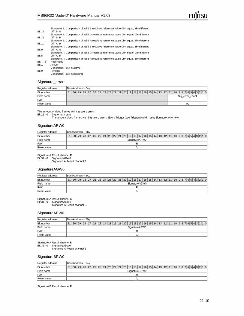
MB86R02 ‘Jade-D’ Hardware Manual V1.63
21-10
Signature B: Comparison of valid B result vs reference value 0b= equal, 1b=different Bit 17 Diff_B_G
Signature B: Comparison of valid G result vs reference value 0b= equal, 1b=different Bit 16 Diff_B_R
Signature B: Comparison of valid R result vs reference value 0b= equal, 1b=different Bit 10 Diff_A_B
Signature A: Comparison of valid B result vs reference value 0b= equal, 1b=different Bit 9 Diff_A_G
Signature A: Comparison of valid G result vs reference value 0b= equal, 1b=different Bit 8 Diff_A_R
Signature A: Comparison of valid R result vs reference value 0b= equal, 1b=different Bit 7 - 5 Reserved2 Bit 1 Active
Generation Task is active Bit 0 Pending
Generation Task is pending
Signature_error
Register address BaseAddress + 64H
Bit number 31 30 29 28 27 26 25 24 23 22 21 20 19 18 17 16 15 14 13 12 11 10 9 8 7 6 5 4 3 2 1 0
Field name Sig_error_count
R/W R
Reset value 0H
The amount of video frames with signature errors Bit 11 - 0 Sig_error_count
The amount video frames with Signature errors. Every Trigger (see TriggerW0) will reset Signature_error to 0
SignatureARW0
Register address BaseAddress + 68H
Bit number 31 30 29 28 27 26 25 24 23 22 21 20 19 18 17 16 15 14 13 12 11 10 9 8 7 6 5 4 3 2 1 0
Field name SignatureARW0
R/W R
Reset value 0H
Signature A Result channel R Bit 31 - 0 SignatureARW0
Signature A Result channel R
SignatureAGW0
Register address BaseAddress + 6CH
Bit number 31 30 29 28 27 26 25 24 23 22 21 20 19 18 17 16 15 14 13 12 11 10 9 8 7 6 5 4 3 2 1 0
Field name SignatureAGW0
R/W R
Reset value 0H
Signature A Result channel G Bit 31 - 0 SignatureAGW0
Signature A Result channel G
SignatureABW0
Register address BaseAddress + 70H
Bit number 31 30 29 28 27 26 25 24 23 22 21 20 19 18 17 16 15 14 13 12 11 10 9 8 7 6 5 4 3 2 1 0
Field name SignatureABW0
R/W R
Reset value 0H
Signature A Result channel B Bit 31 - 0 SignatureABW0
Signature A Result channel B
SignatureBRW0
Register address BaseAddress + 74H
Bit number 31 30 29 28 27 26 25 24 23 22 21 20 19 18 17 16 15 14 13 12 11 10 9 8 7 6 5 4 3 2 1 0
Field name SignatureBRW0
R/W R
Reset value 0H
Signature B Result channel R

MB86R02 ‘Jade-D’ Hardware Manual V1.63
21-11
Bit 31 - 0 SignatureBRW0 Signature B Result channel R
SignatureBGW0
Register address BaseAddress + 78H
Bit number 31 30 29 28 27 26 25 24 23 22 21 20 19 18 17 16 15 14 13 12 11 10 9 8 7 6 5 4 3 2 1 0
Field name SignatureBGW0
R/W R
Reset value 0H
Signature B Result channel G Bit 31 - 0 SignatureBGW0
Signature B Result channel G
SignatureBBW0
Register address BaseAddress + 7CH
Bit number 31 30 29 28 27 26 25 24 23 22 21 20 19 18 17 16 15 14 13 12 11 10 9 8 7 6 5 4 3 2 1 0
Field name SignatureBBW0
R/W R
Reset value 0H
Signature B Result channel B Bit 31 - 0 SignatureBBW0
Signature B Result channel B

MB86R02 ‘Jade-D’ Hardware Manual V1.63
21-12
21.5 Processing Mode
21.5.1 Processing Flow
Figure 21-2 SIG Processing Flow
21.5.2 Processing Algorithm Please see chapter 21.3 Checksum generations are possible for each incoming pixel frame. When a generation is triggerered, after each incoming pixel frame, a set of signature checksum results is valid.

MB86R02 ‘Jade-D’ Hardware Manual V1.63
21-13
21.6 Control Flow
21.6.1 Example Control Flow
IStsCfgCopy
Config Bus wr 0 rd 0
CtrlCfg.trigger
Status.pending
Status.active
Frame Start
IStsResValid
wr 1 wr 2 rd 1 rd 2
Cleared by SW
Figure 21-3 Example Control Flow 1

MB86R02 ‘Jade-D’ Hardware Manual V1.63
21-14
Figure 21-4, Example Control Flow 2

MB86R02 ‘Jade-D’ Hardware Manual V1.63
21-15
21.6.2 Signature Generation with every incoming frame General Configuration phase: (most registers are not shadowed) Enable mask mode Write mask window coordinates Enable Signatures types Enable interrupts Configuration phase for calculation 0 Write Window 0 coordinates Set Triggermode to one single generation Trigger one generation by writing ‘1’ to the trigger field Wait on interrupt or poll IStsCfgCop, IStsResVal On IStsCfgCop Configuration phase for calculation n Write Window n coordinates Setup single TriggerMode Trigger one generation by writing to the trigger field On IStsResVal Read result registers Signature A (B) Process results
21.6.3 Cyclic Signature Generation with every incoming frame CYCLIC monitoring of one window: General Configuration phase: (most registers are not shadowed) Enable mask mode Write mask window coordinates Enable Signatures types Enable interrupts Configuration phase for calculation 0 Write Window 0 coordinates Setup cyclic TriggerMode Trigger cyclic generation by writing ‘1’ to the trigger field Wait on interrupt or poll IStsResVal On IStsResVal Read result registers Signature A, (B) Process results

MB86R02 ‘Jade-D’ Hardware Manual V1.63
21-16
21.6.4 Cyclic Signature Generation with every incoming frame, limiting read accesses
Cyclic for one window, with interrupt monitoring General Configuration phase: (not shadowed registers) Enable mask mode Write mask window coordinates Enable Signatures types Enable interrupts Configuration phase for calculation 0 Write Window 0 coordinates Write reference values for Signature A (Write reference values for Signature B, Set threshold for B) Setup cyclic TriggerMode Trigger cyclic generation by writing ‘1’ to the trigger field Wait on interrupt or poll IStsDiff On IStsDiff
Read result registers Signature A, (B) Process results Before display content of evaluation window changes: Cancel cyclic trigger and reprogram reference values
21.6.5 Limitation of Cyclic Signature Generation It is not recommended to change evaluation window coordinates and relating reference values during cyclic (= continuous) monitoring mode. Reference value registers are overtaken with every frame start. Coordinate registers are overtaken only after write of Register TriggerW0.Trigger. If nevertheless cyclic mode is used the following real time requirement exists for the configuration of coordinate and reference registers: The update of coordinate and reference registers must be finished within one video frame.

MB86R02 ‘Jade-D’ Hardware Manual V1.63
22-1
22 Timing Controller (TCON)
22.1 Position of Block in whole LSI
Figure 22-1 Location of the TCON in the GDC
22.2 Overview The Timing Controller module TCON allows the generation of control signals and data signals for direct interfacing to the column and row drivers of a display panel. The freely programmable waveform of the generated timing control signals allows the emulation of almost every timing controller IC (TCON IC) commonly used in display panels. The RGB data is transmitted as single-ended TTL signals or as low voltage differential swing signals conforming to the RSDS™ standard (Reduced Swing Differential Signal). The module consists of three submodules; a Timing Signal Generator (TSIG) module, an RSDS™ bit mapping module (RBM) and an IO module for control of special RSDS™ or TTL capable IO-cells. The TSIG IP is derived from Fujitsu’s MB87P2020 (Jasmine) SyncSig IP (please refer to the MB87P2020 Hardware Manual).
22.3 Feature List RBM (RSDS Bit Mapping)
Conforms to RSDS™ Standard 1.0 (National Semiconductors)
Support for single bus (Multidrop bus with single or double end termination)
Mapping for 6 bit color depth
Mapping for 8 bit color depth
Data and clock outputs can flexible be assigned to the pool of available pins to ease board design
References: RSDS™ “Intra-Panel” Interface Specification, Revision 1.0, May 2003, (National Semiconductor Corporation©)
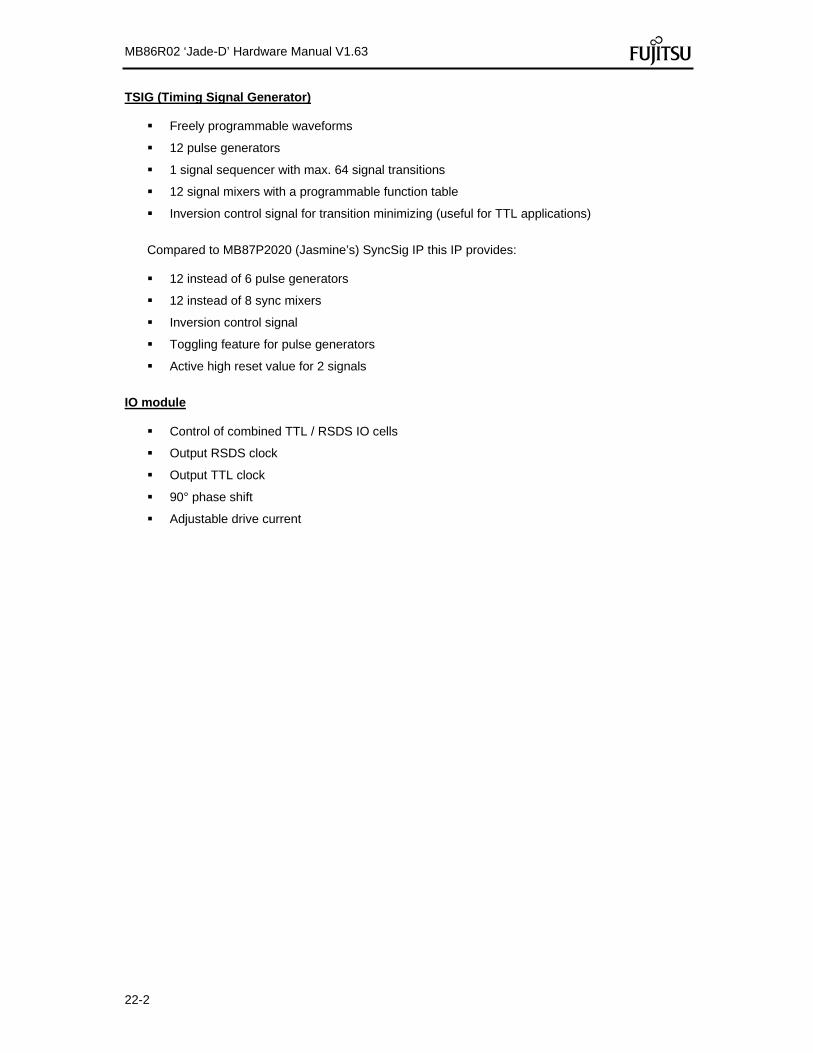
MB86R02 ‘Jade-D’ Hardware Manual V1.63
22-2
TSIG (Timing Signal Generator)
Freely programmable waveforms
12 pulse generators
1 signal sequencer with max. 64 signal transitions
12 signal mixers with a programmable function table
Inversion control signal for transition minimizing (useful for TTL applications)
Compared to MB87P2020 (Jasmine’s) SyncSig IP this IP provides:
12 instead of 6 pulse generators
12 instead of 8 sync mixers
Inversion control signal
Toggling feature for pulse generators
Active high reset value for 2 signals
IO module
Control of combined TTL / RSDS IO cells
Output RSDS clock
Output TTL clock
90° phase shift
Adjustable drive current

MB86R02 ‘Jade-D’ Hardware Manual V1.63
22-3
22.4 Software Interface Format of Register Description The register descriptions in the following sections use the format shown below to describe each bit field of a register. Register address Offset
Bit number 31 30 29 28 27 26 25 24 23 22 21 20 19 18 17 16 15 14 13 12 11 10 9 8 7 6 5 4 3 2 1 0
Field name
R/W
Reset value
Meaning of items and sign Register address
Register address shows the address (Offset address) of the register. Bit number
Bit number shows bit position of the register. Field name
Field name shows bit name of the register. R/W
R/W shows the read/write attribute of each bit field: R: Read W: Write W1C: Writing a value of "1" clears the register.
Reset value Reset value indicates the value of each bit field immediately after reset. 0: Initial value is "0". 1: Initial value is "1". X: Undefined.
Unused register fields are marked with a solid grey background. Bit vectors are unsigned integers, if nothing else specified. Please note, that access to an address with no register results in an error response. Global Address For module base address refer to inter-module specification or global address map of the respective LSI. Register Summary
Address Register Name DescriptionBase address + 0H
: Base address +
FFH
DIR_SSqCnts Sequencer position definitions, only 32 bit word access is supported
Base address + 400H
DIR_SWreset TCON Software Reset
Base address + 404H
DIR_SPG0PosOn Sync pulse generator 0, 'Switch on' position
Base address + 408H
DIR_SPG0MaskOn
Base address + DIR_SPG0PosOff Sync pulse generator 0, 'Switch off' position
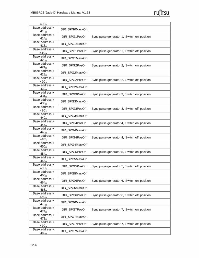
MB86R02 ‘Jade-D’ Hardware Manual V1.63
22-4
40CH Base address +
410H DIR_SPG0MaskOff
Base address + 414H
DIR_SPG1PosOn Sync pulse generator 1, 'Switch on' position
Base address + 418H
DIR_SPG1MaskOn
Base address + 41CH
DIR_SPG1PosOff Sync pulse generator 1, 'Switch off' position
Base address + 420H
DIR_SPG1MaskOff
Base address + 424H
DIR_SPG2PosOn Sync pulse generator 2, 'Switch on' position
Base address + 428H
DIR_SPG2MaskOn
Base address + 42CH
DIR_SPG2PosOff Sync pulse generator 2, 'Switch off' position
Base address + 430H
DIR_SPG2MaskOff
Base address + 434H
DIR_SPG3PosOn Sync pulse generator 3, 'Switch on' position
Base address + 438H
DIR_SPG3MaskOn
Base address + 43CH
DIR_SPG3PosOff Sync pulse generator 3, 'Switch off' position
Base address + 440H
DIR_SPG3MaskOff
Base address + 444H
DIR_SPG4PosOn Sync pulse generator 4, 'Switch on' position
Base address + 448H
DIR_SPG4MaskOn
Base address + 44CH
DIR_SPG4PosOff Sync pulse generator 4, 'Switch off' position
Base address + 450H
DIR_SPG4MaskOff
Base address + 454H
DIR_SPG5PosOn Sync pulse generator 5, 'Switch on' position
Base address + 458H
DIR_SPG5MaskOn
Base address + 45CH
DIR_SPG5PosOff Sync pulse generator 5, 'Switch off' position
Base address + 460H
DIR_SPG5MaskOff
Base address + 464H
DIR_SPG6PosOn Sync pulse generator 6, 'Switch on' position
Base address + 468H
DIR_SPG6MaskOn
Base address + 46CH
DIR_SPG6PosOff Sync pulse generator 6, 'Switch off' position
Base address + 470H
DIR_SPG6MaskOff
Base address + 474H
DIR_SPG7PosOn Sync pulse generator 7, 'Switch on' position
Base address + 478H
DIR_SPG7MaskOn
Base address + 47CH
DIR_SPG7PosOff Sync pulse generator 7, 'Switch off' position
Base address + 480H
DIR_SPG7MaskOff

MB86R02 ‘Jade-D’ Hardware Manual V1.63
22-5
Base address + 484H
DIR_SPG8PosOn Sync pulse generator 8, 'Switch on' position
Base address + 488H
DIR_SPG8MaskOn
Base address + 48CH
DIR_SPG8PosOff Sync pulse generator 8, 'Switch off' position
Base address + 490H
DIR_SPG8MaskOff
Base address + 494H
DIR_SPG9PosOn Sync pulse generator 9, 'Switch on' position
Base address + 498H
DIR_SPG9MaskOn
Base address + 49CH
DIR_SPG9PosOff Sync pulse generator 9, 'Switch off' position
Base address + 4A0H
DIR_SPG9MaskOff
Base address + 4A4H
DIR_SPG10PosOn Sync pulse generator 10, 'Switch on' position
Base address + 4A8H
DIR_SPG10MaskOn
Base address + 4ACH
DIR_SPG10PosOff Sync pulse generator 10, 'Switch off' position
Base address + 4B0H
DIR_SPG10MaskOff
Base address + 4B4H
DIR_SPG11PosOn Sync pulse generator 11, 'Switch on' position
Base address + 4B8H
DIR_SPG11MaskOn
Base address + 4BCH
DIR_SPG11PosOff Sync pulse generator 11, 'Switch off' position
Base address + 4C0H
DIR_SPG11MaskOff
Base address + 4C4H
DIR_SSqCycle
Base address + 4C8H
DIR_SMx0Sigs Sync mixer 0 signal selection
Base address + 4CCH
DIR_SMx0FctTable Sync mixer output = function table [a] a = s4*24+s3*23+s2*22+s1*21+s0*20
Base address + 4D0H
DIR_SMx1Sigs Sync mixer 1 signal selection
Base address + 4D4H
DIR_SMx1FctTable Sync mixer output = function table [a] a = s4*24+s3*23+s2*22+s1*21+s0*20
Base address + 4D8H
DIR_SMx2Sigs Sync mixer 2 signal selection
Base address + 4DCH
DIR_SMx2FctTable Sync mixer output = function table [a] a = s4*24+s3*23+s2*22+s1*21+s0*20
Base address + 4E0H
DIR_SMx3Sigs Sync mixer 3 signal selection
Base address + 4E4H
DIR_SMx3FctTable Sync mixer output = function table [a] a = s4*24+s3*23+s2*22+s1*21+s0*20
Base address + 4E8H
DIR_SMx4Sigs Sync mixer 4 signal selection
Base address + 4ECH
DIR_SMx4FctTable Sync mixer output = function table [a] a = s4*24+s3*23+s2*22+s1*21+s0*20
Base address + 4F0H
DIR_SMx5Sigs Sync mixer 5 signal selection
Base address + 4F4H
DIR_SMx5FctTable Sync mixer output = function table [a] a = s4*24+s3*23+s2*22+s1*21+s0*20
Base address + DIR_SMx6Sigs Sync mixer 6 signal selection

MB86R02 ‘Jade-D’ Hardware Manual V1.63
22-6
4F8H Base address +
4FCH DIR_SMx6FctTable
Sync mixer output = function table [a] a = s4*24+s3*23+s2*22+s1*21+s0*20
Base address + 500H
DIR_SMx7Sigs Sync mixer 7 signal selection
Base address + 504H
DIR_SMx7FctTable Sync mixer output = function table [a] a = s4*24+s3*23+s2*22+s1*21+s0*20
Base address + 508H
DIR_SMx8Sigs Sync mixer 8 signal selection
Base address + 50CH
DIR_SMx8FctTable Sync mixer output = function table [a] a = s4*24+s3*23+s2*22+s1*21+s0*20
Base address + 510H
DIR_SMx9Sigs Sync mixer 9 signal selection
Base address + 514H
DIR_SMx9FctTable Sync mixer output = function table [a] a = s4*24+s3*23+s2*22+s1*21+s0*20
Base address + 518H
DIR_SMx10Sigs Sync mixer 10 signal selection
Base address + 51CH
DIR_SMx10FctTable Sync mixer output = function table [a] a = s4*24+s3*23+s2*22+s1*21+s0*20
Base address + 520H
DIR_SMx11Sigs Sync mixer 11 signal selection
Base address + 524H
DIR_SMx11FctTable Sync mixer output = function table [a] a = s4*24+s3*23+s2*22+s1*21+s0*20
Base address + 528H
DIR_SSwitch Sync switch
Base address + 52CH
DIR_RBM_CTRL RSDS Bitmap Control
Base address + 534H
DIR_PIN0_CTRL IO Module Pad 0 Control
Base address + 538H
DIR_PIN1_CTRL IO Module Pad 1 Control
Base address + 53CH
DIR_PIN2_CTRL IO Module Pad 2 Control
Base address + 540H
DIR_PIN3_CTRL IO Module Pad 3 Control
Base address + 544H
DIR_PIN4_CTRL IO Module Pad 4 Control
Base address + 548H
DIR_PIN5_CTRL IO Module Pad 5 Control
Base address + 54CH
DIR_PIN6_CTRL IO Module Pad 6 Control
Base address + 550H
DIR_PIN7_CTRL IO Module Pad 7 Control
Base address + 554H
DIR_PIN8_CTRL IO Module Pad 8 Control
Base address + 558H
DIR_PIN9_CTRL IO Module Pad 9 Control
Base address + 55CH
DIR_PIN10_CTRL IO Module Pad 10 Control
Base address + 560H
DIR_PIN11_CTRL IO Module Pad 11 Control
Base address + 564H
DIR_PIN12_CTRL IO Module Pad 12 Control
Register Description DIR_SSqCnts [0...63]

MB86R02 ‘Jade-D’ Hardware Manual V1.63
22-7
Register address BaseAddress + 0H : BaseAddress + FFH
Bit number 31 30 29 28 27 26 25 24 23 22 21 20 19 18 17 16 15 14 13 12 11 10 9 8 7 6 5 4 3 2 1 0
Field name SSQCNTS_OUT SSQCNTS_SEQX Reserved SSQCNTS_SEQY
R/W RW RW RW RW
Reset value X X X X
Sequencer position definitions, only 32 bit word access is supported Bit 31 SSQCNTS_OUT
Output value, when position is reached Bit 30 - 16 SSQCNTS_SEQX
X scan position Bit 15 Reserved
Do not modify Bit 14 - 0 SSQCNTS_SEQY
Y scan position
DIR_SWreset
Register address BaseAddress + 400H
Bit number 31 30 29 28 27 26 25 24 23 22 21 20 19 18 17 16 15 14 13 12 11 10 9 8 7 6 5 4 3 2 1 0
Field name SWReset
R/W RW
Reset value 1H
TCON Software Reset Bit 0
SWReset Software reset: write 0b=no effect, 1b=activate Reset, SW reset is deasserted by internal logic), read: 0b: reset not active 1b: reset active (that means no last pixel of video frame was input to TCON since last activation of sw-reset)
DIR_SPG0PosOn
Register address BaseAddress + 404H
Bit number 31 30 29 28 27 26 25 24 23 22 21 20 19 18 17 16 15 14 13 12 11 10 9 8 7 6 5 4 3 2 1 0
Field name SPGPSON_TOGGLE0 SPGPSON_X0 Reserved SPGPSON_Y0
R/W RW RW RW RW
Reset value 0H 0H 0H 0H
Sync pulse generator 0, 'Switch on' position Bit 31 SPGPSON_TOGGLE0
Toggle enable: 0b=disable, 1b=enable Bit 30 - 16 SPGPSON_X0
X scan position Bit 15 Reserved
Do not modify Bit 14 - 0 SPGPSON_Y0
Y scan position
DIR_SPG0MaskOn
Register address BaseAddress + 408H
Bit number 31 30 29 28 27 26 25 24 23 22 21 20 19 18 17 16 15 14 13 12 11 10 9 8 7 6 5 4 3 2 1 0
Field name SPGMKON0
R/W RW
Reset value 0H
Bit 30 - 0 SPGMKON0
Mask bits: 0b=include bit in position matching, 1b= do not include this bit in position matching
DIR_SPG0PosOff
Register address BaseAddress + 40CH
Bit number 31 30 29 28 27 26 25 24 23 22 21 20 19 18 17 16 15 14 13 12 11 10 9 8 7 6 5 4 3 2 1 0
Field name SPGPSOFF_TOGGLE0 SPGPSOFF_X0 Reserved SPGPSOFF_Y0
R/W RW RW RW RW
Reset value 0H 0H 0H 0H
Sync pulse generator 0, 'Switch off' position Bit 31 SPGPSOFF_TOGGLE0
Toggle enable: 0b=disable, 1b=enable Bit 30 - 16 SPGPSOFF_X0
X scan position Bit 15 Reserved
Do not modify

MB86R02 ‘Jade-D’ Hardware Manual V1.63
22-8
Bit 14 - 0 SPGPSOFF_Y0 Y scan position
DIR_SPG0MaskOff
Register address BaseAddress + 410H
Bit number 31 30 29 28 27 26 25 24 23 22 21 20 19 18 17 16 15 14 13 12 11 10 9 8 7 6 5 4 3 2 1 0
Field name SPGMKOFF0
R/W RW
Reset value 0H
Bit 30 - 0 SPGMKOFF0
Mask bits: 0b=include bit in position matching, 1b= do not include this bit in position matching
DIR_SPG1PosOn
Register address BaseAddress + 414H
Bit number 31 30 29 28 27 26 25 24 23 22 21 20 19 18 17 16 15 14 13 12 11 10 9 8 7 6 5 4 3 2 1 0
Field name SPGPSON_TOGGLE1 SPGPSON_X1 Reserved SPGPSON_Y1
R/W RW RW RW RW
Reset value 0H 0H 0H 0H
Sync pulse generator 1, 'Switch on' position Bit 31 SPGPSON_TOGGLE1
Toggle enable: 0b=disable, 1b=enable Bit 30 - 16 SPGPSON_X1
X scan position Bit 15 Reserved
Do not modify Bit 14 - 0 SPGPSON_Y1
Y scan position
DIR_SPG1MaskOn
Register address BaseAddress + 418H
Bit number 31 30 29 28 27 26 25 24 23 22 21 20 19 18 17 16 15 14 13 12 11 10 9 8 7 6 5 4 3 2 1 0
Field name SPGMKON1
R/W RW
Reset value 0H
Bit 30 - 0 SPGMKON1
mask bits (1= do not include this bit into position matching)
DIR_SPG1PosOff
Register address BaseAddress + 41CH
Bit number 31 30 29 28 27 26 25 24 23 22 21 20 19 18 17 16 15 14 13 12 11 10 9 8 7 6 5 4 3 2 1 0
Field name SPGPSOFF_TOGGLE1 SPGPSOFF_X1 Reserved SPGPSOFF_Y1
R/W RW RW RW RW
Reset value 0H 0H 0H 0H
Sync pulse generator 1, 'Switch off' position Bit 31 SPGPSOFF_TOGGLE1
Toggle enable: 0b=disable, 1b=enable Bit 30 - 16 SPGPSOFF_X1
X scan position Bit 15 Reserved
Do not modify Bit 14 - 0 SPGPSOFF_Y1
Y scan position
DIR_SPG1MaskOff
Register address BaseAddress + 420H
Bit number 31 30 29 28 27 26 25 24 23 22 21 20 19 18 17 16 15 14 13 12 11 10 9 8 7 6 5 4 3 2 1 0
Field name SPGMKOFF1
R/W RW
Reset value 0H
Bit 30 - 0 SPGMKOFF1
Mask bits: 0b=include bit in position matching, 1b= do not include this bit in position matching
DIR_SPG2PosOn

MB86R02 ‘Jade-D’ Hardware Manual V1.63
22-9
Register address BaseAddress + 424H
Bit number 31 30 29 28 27 26 25 24 23 22 21 20 19 18 17 16 15 14 13 12 11 10 9 8 7 6 5 4 3 2 1 0
Field name SPGPSON_TOGGLE2 SPGPSON_X2 Reserved SPGPSON_Y2
R/W RW RW RW RW
Reset value 0H 0H 0H 0H
Sync pulse generator 2, 'Switch on' position Bit 31 SPGPSON_TOGGLE2
Toggle enable: 0b=disable, 1b=enable Bit 30 - 16 SPGPSON_X2
X scan position Bit 15 Reserved
Do not modify Bit 14 - 0 SPGPSON_Y2
Y scan position
DIR_SPG2MaskOn
Register address BaseAddress + 428H
Bit number 31 30 29 28 27 26 25 24 23 22 21 20 19 18 17 16 15 14 13 12 11 10 9 8 7 6 5 4 3 2 1 0
Field name SPGMKON2
R/W RW
Reset value 0H
Bit 30 - 0 SPGMKON2
Mask bits: 0b=include bit in position matching, 1b= do not include this bit in position matching
DIR_SPG2PosOff
Register address BaseAddress + 42CH
Bit number 31 30 29 28 27 26 25 24 23 22 21 20 19 18 17 16 15 14 13 12 11 10 9 8 7 6 5 4 3 2 1 0
Field name SPGPSOFF_TOGGLE2 SPGPSOFF_X2 Reserved SPGPSOFF_Y2
R/W RW RW RW RW
Reset value 0H 0H 0H 0H
Sync pulse generator 2, 'Switch off' position Bit 31 SPGPSOFF_TOGGLE2
Toggle enable: 0b=disable, 1b=enable Bit 30 - 16 SPGPSOFF_X2
X scan position Bit 15 Reserved
Do not modify Bit 14 - 0 SPGPSOFF_Y2
Y scan position
DIR_SPG2MaskOff
Register address BaseAddress + 430H
Bit number 31 30 29 28 27 26 25 24 23 22 21 20 19 18 17 16 15 14 13 12 11 10 9 8 7 6 5 4 3 2 1 0
Field name SPGMKOFF2
R/W RW
Reset value 0H
Bit 30 - 0 SPGMKOFF2
Mask bits: 0b=include bit in position matching, 1b= do not include this bit in position matching
DIR_SPG3PosOn
Register address BaseAddress + 434H
Bit number 31 30 29 28 27 26 25 24 23 22 21 20 19 18 17 16 15 14 13 12 11 10 9 8 7 6 5 4 3 2 1 0
Field name SPGPSON_TOGGLE3 SPGPSON_X3 Reserved SPGPSON_Y3
R/W RW RW RW RW
Reset value 0H 0H 0H 0H
Sync pulse generator 3, 'Switch on' position Bit 31 SPGPSON_TOGGLE3
Toggle enable: 0b=disable, 1b=enable Bit 30 - 16 SPGPSON_X3
X scan position Bit 15 Reserved
Do not modify Bit 14 - 0 SPGPSON_Y3
Y scan position

MB86R02 ‘Jade-D’ Hardware Manual V1.63
22-10
DIR_SPG3MaskOn
Register address BaseAddress + 438H
Bit number 31 30 29 28 27 26 25 24 23 22 21 20 19 18 17 16 15 14 13 12 11 10 9 8 7 6 5 4 3 2 1 0
Field name SPGMKON3
R/W RW
Reset value 0H
Bit 30 - 0 SPGMKON3
Mask bits: 0b=include bit in position matching, 1b= do not include this bit in position matching
DIR_SPG3PosOff
Register address BaseAddress + 43CH
Bit number 31 30 29 28 27 26 25 24 23 22 21 20 19 18 17 16 15 14 13 12 11 10 9 8 7 6 5 4 3 2 1 0
Field name SPGPSOFF_TOGGLE3 SPGPSOFF_X3 Reserved SPGPSOFF_Y3
R/W RW RW RW RW
Reset value 0H 0H 0H 0H
Sync pulse generator 3, 'Switch off' position Bit 31 SPGPSOFF_TOGGLE3
Toggle enable: 0b=disable, 1b=enable Bit 30 - 16 SPGPSOFF_X3
X scan position Bit 15 Reserved
Do not modify Bit 14 - 0 SPGPSOFF_Y3
Y scan position
DIR_SPG3MaskOff
Register address BaseAddress + 440H
Bit number 31 30 29 28 27 26 25 24 23 22 21 20 19 18 17 16 15 14 13 12 11 10 9 8 7 6 5 4 3 2 1 0
Field name SPGMKOFF3
R/W RW
Reset value 0H
Bit 30 - 0 SPGMKOFF3
Mask bits: 0b=include bit in position matching, 1b= do not include this bit in position matching
DIR_SPG4PosOn
Register address BaseAddress + 444H
Bit number 31 30 29 28 27 26 25 24 23 22 21 20 19 18 17 16 15 14 13 12 11 10 9 8 7 6 5 4 3 2 1 0
Field name SPGPSON_TOGGLE4 SPGPSON_X4 Reserved SPGPSON_Y4
R/W RW RW RW RW
Reset value 0H 0H 0H 0H
Sync pulse generator 4, 'Switch on' position Bit 31 SPGPSON_TOGGLE4
Toggle enable: 0b=disable, 1b=enable Bit 30 - 16 SPGPSON_X4
X scan position Bit 15 Reserved
Do not modify Bit 14 - 0 SPGPSON_Y4
Y scan position
DIR_SPG4MaskOn
Register address BaseAddress + 448H
Bit number 31 30 29 28 27 26 25 24 23 22 21 20 19 18 17 16 15 14 13 12 11 10 9 8 7 6 5 4 3 2 1 0
Field name SPGMKON4
R/W RW
Reset value 0H
Bit 30 - 0 SPGMKON4
Mask bits: 0b=include bit in position matching, 1b= do not include this bit in position matching
DIR_SPG4PosOff
Register address BaseAddress + 44CH
Bit number 31 30 29 28 27 26 25 24 23 22 21 20 19 18 17 16 15 14 13 12 11 10 9 8 7 6 5 4 3 2 1 0

MB86R02 ‘Jade-D’ Hardware Manual V1.63
22-11
Field name SPGPSOFF_TOGGLE4 SPGPSOFF_X4 Reserved SPGPSOFF_Y4
R/W RW RW RW RW
Reset value 0H 0H 0H 0H
Sync pulse generator 4, 'Switch off' position Bit 31 SPGPSOFF_TOGGLE4
Toggle enable: 0b=disable, 1b=enable Bit 30 - 16 SPGPSOFF_X4
X scan position Bit 15 Reserved
Do not modify Bit 14 - 0 SPGPSOFF_Y4
Y scan position
DIR_SPG4MaskOff
Register address BaseAddress + 450H
Bit number 31 30 29 28 27 26 25 24 23 22 21 20 19 18 17 16 15 14 13 12 11 10 9 8 7 6 5 4 3 2 1 0
Field name SPGMKOFF4
R/W RW
Reset value 0H
Bit 30 - 0 SPGMKOFF4
Mask bits: 0b=include bit in position matching, 1b= do not include this bit in position matching
DIR_SPG5PosOn
Register address BaseAddress + 454H
Bit number 31 30 29 28 27 26 25 24 23 22 21 20 19 18 17 16 15 14 13 12 11 10 9 8 7 6 5 4 3 2 1 0
Field name SPGPSON_TOGGLE5 SPGPSON_X5 Reserved SPGPSON_Y5
R/W RW RW RW RW
Reset value 0H 0H 0H 0H
Sync pulse generator 5, 'Switch on' position Bit 31 SPGPSON_TOGGLE5
Toggle enable: 0b=disable, 1b=enable Bit 30 - 16 SPGPSON_X5
X scan position Bit 15 Reserved
Do not modify Bit 14 - 0 SPGPSON_Y5
Y scan position
DIR_SPG5MaskOn
Register address BaseAddress + 458H
Bit number 31 30 29 28 27 26 25 24 23 22 21 20 19 18 17 16 15 14 13 12 11 10 9 8 7 6 5 4 3 2 1 0
Field name SPGMKON5
R/W RW
Reset value 0H
Bit 30 - 0 SPGMKON5
Mask bits: 0b=include bit in position matching, 1b= do not include this bit in position matching
DIR_SPG5PosOff
Register address BaseAddress + 45CH
Bit number 31 30 29 28 27 26 25 24 23 22 21 20 19 18 17 16 15 14 13 12 11 10 9 8 7 6 5 4 3 2 1 0
Field name SPGPSOFF_TOGGLE5 SPGPSOFF_X5 Reserved SPGPSOFF_Y5
R/W RW RW RW RW
Reset value 0H 0H 0H 0H
Sync pulse generator 5, 'Switch off' position Bit 31 SPGPSOFF_TOGGLE5
Toggle enable: 0b=disable, 1b=enable Bit 30 - 16 SPGPSOFF_X5
X scan position Bit 15 Reserved
Do not modify Bit 14 - 0 SPGPSOFF_Y5
Y scan position
DIR_SPG5MaskOff

MB86R02 ‘Jade-D’ Hardware Manual V1.63
22-12
Register address BaseAddress + 460H
Bit number 31 30 29 28 27 26 25 24 23 22 21 20 19 18 17 16 15 14 13 12 11 10 9 8 7 6 5 4 3 2 1 0
Field name SPGMKOFF5
R/W RW
Reset value 0H
Bit 30 - 0 SPGMKOFF5
Mask bits: 0b=include bit in position matching, 1b= do not include this bit in position matching
DIR_SPG6PosOn
Register address BaseAddress + 464H
Bit number 31 30 29 28 27 26 25 24 23 22 21 20 19 18 17 16 15 14 13 12 11 10 9 8 7 6 5 4 3 2 1 0
Field name SPGPSON_TOGGLE6 SPGPSON_X6 Reserved SPGPSON_Y6
R/W RW RW RW RW
Reset value 0H 0H 0H 0H
Sync pulse generator 6, 'Switch on' position Bit 31 SPGPSON_TOGGLE6
Toggle enable: 0b=disable, 1b=enable Bit 30 - 16 SPGPSON_X6
X scan position Bit 15 Reserved
Do not modify Bit 14 - 0 SPGPSON_Y6
Y scan position
DIR_SPG6MaskOn
Register address BaseAddress + 468H
Bit number 31 30 29 28 27 26 25 24 23 22 21 20 19 18 17 16 15 14 13 12 11 10 9 8 7 6 5 4 3 2 1 0
Field name SPGMKON6
R/W RW
Reset value 0H
Bit 30 - 0 SPGMKON6
Mask bits: 0b=include bit in position matching, 1b= do not include this bit in position matching
DIR_SPG6PosOff
Register address BaseAddress + 46CH
Bit number 31 30 29 28 27 26 25 24 23 22 21 20 19 18 17 16 15 14 13 12 11 10 9 8 7 6 5 4 3 2 1 0
Field name SPGPSOFF_TOGGLE6 SPGPSOFF_X6 Reserved SPGPSOFF_Y6
R/W RW RW RW RW
Reset value 0H 0H 0H 0H
Sync pulse generator 6, 'Switch off' position Bit 31 SPGPSOFF_TOGGLE6
Toggle enable: 0b=disable, 1b=enable Bit 30 - 16 SPGPSOFF_X6
X scan position Bit 15 Reserved
Do not modify Bit 14 - 0 SPGPSOFF_Y6
Y scan position
DIR_SPG6MaskOff
Register address BaseAddress + 470H
Bit number 31 30 29 28 27 26 25 24 23 22 21 20 19 18 17 16 15 14 13 12 11 10 9 8 7 6 5 4 3 2 1 0
Field name SPGMKOFF6
R/W RW
Reset value 0H
Bit 30 - 0 SPGMKOFF6
Mask bits: 0b=include bit in position matching, 1b= do not include this bit in position matching
DIR_SPG7PosOn
Register address BaseAddress + 474H
Bit number 31 30 29 28 27 26 25 24 23 22 21 20 19 18 17 16 15 14 13 12 11 10 9 8 7 6 5 4 3 2 1 0
Field name SPGPSON_TOGGLE7 SPGPSON_X7 Reserved SPGPSON_Y7
R/W RW RW RW RW

MB86R02 ‘Jade-D’ Hardware Manual V1.63
22-13
Reset value 0H 0H 0H 0H
Sync pulse generator 7, 'Switch on' position Bit 31 SPGPSON_TOGGLE7
Toggle enable: 0b=disable, 1b=enable Bit 30 - 16 SPGPSON_X7
X scan position Bit 15 Reserved
Do not modify Bit 14 - 0 SPGPSON_Y7
Y scan position
DIR_SPG7MaskOn
Register address BaseAddress + 478H
Bit number 31 30 29 28 27 26 25 24 23 22 21 20 19 18 17 16 15 14 13 12 11 10 9 8 7 6 5 4 3 2 1 0
Field name SPGMKON7
R/W RW
Reset value 0H
Bit 30 - 0 SPGMKON7
Mask bits: 0b=include bit in position matching, 1b= do not include this bit in position matching
DIR_SPG7PosOff
Register address BaseAddress + 47CH
Bit number 31 30 29 28 27 26 25 24 23 22 21 20 19 18 17 16 15 14 13 12 11 10 9 8 7 6 5 4 3 2 1 0
Field name SPGPSOFF_TOGGLE7 SPGPSOFF_X7 Reserved SPGPSOFF_Y7
R/W RW RW RW RW
Reset value 0H 0H 0H 0H
Sync pulse generator 7, 'Switch off' position Bit 31 SPGPSOFF_TOGGLE7
Toggle enable: 0b=disable, 1b=enable Bit 30 - 16 SPGPSOFF_X7
X scan position Bit 15 Reserved
Do not modify Bit 14 - 0 SPGPSOFF_Y7
Y scan position
DIR_SPG7MaskOff
Register address BaseAddress + 480H
Bit number 31 30 29 28 27 26 25 24 23 22 21 20 19 18 17 16 15 14 13 12 11 10 9 8 7 6 5 4 3 2 1 0
Field name SPGMKOFF7
R/W RW
Reset value 0H
Bit 30 - 0 SPGMKOFF7
Mask bits: 0b=include bit in position matching, 1b= do not include this bit in position matching
DIR_SPG8PosOn
Register address BaseAddress + 484H
Bit number 31 30 29 28 27 26 25 24 23 22 21 20 19 18 17 16 15 14 13 12 11 10 9 8 7 6 5 4 3 2 1 0
Field name SPGPSON_TOGGLE8 SPGPSON_X8 Reserved SPGPSON_Y8
R/W RW RW RW RW
Reset value 0H 0H 0H 0H
Sync pulse generator 8, 'Switch on' position Bit 31 SPGPSON_TOGGLE8
Toggle enable: 0b=disable, 1b=enable Bit 30 - 16 SPGPSON_X8
X scan position Bit 15 Reserved
Do not modify Bit 14 - 0 SPGPSON_Y8
Y scan position
DIR_SPG8MaskOn
Register address BaseAddress + 488H
Bit number 31 30 29 28 27 26 25 24 23 22 21 20 19 18 17 16 15 14 13 12 11 10 9 8 7 6 5 4 3 2 1 0
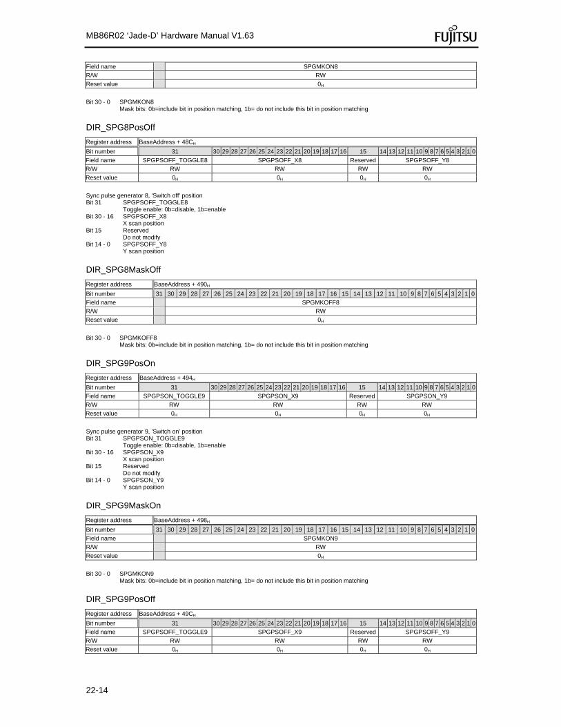
MB86R02 ‘Jade-D’ Hardware Manual V1.63
22-14
Field name SPGMKON8
R/W RW
Reset value 0H
Bit 30 - 0 SPGMKON8
Mask bits: 0b=include bit in position matching, 1b= do not include this bit in position matching
DIR_SPG8PosOff
Register address BaseAddress + 48CH
Bit number 31 30 29 28 27 26 25 24 23 22 21 20 19 18 17 16 15 14 13 12 11 10 9 8 7 6 5 4 3 2 1 0
Field name SPGPSOFF_TOGGLE8 SPGPSOFF_X8 Reserved SPGPSOFF_Y8
R/W RW RW RW RW
Reset value 0H 0H 0H 0H
Sync pulse generator 8, 'Switch off' position Bit 31 SPGPSOFF_TOGGLE8
Toggle enable: 0b=disable, 1b=enable Bit 30 - 16 SPGPSOFF_X8
X scan position Bit 15 Reserved
Do not modify Bit 14 - 0 SPGPSOFF_Y8
Y scan position
DIR_SPG8MaskOff
Register address BaseAddress + 490H
Bit number 31 30 29 28 27 26 25 24 23 22 21 20 19 18 17 16 15 14 13 12 11 10 9 8 7 6 5 4 3 2 1 0
Field name SPGMKOFF8
R/W RW
Reset value 0H
Bit 30 - 0 SPGMKOFF8
Mask bits: 0b=include bit in position matching, 1b= do not include this bit in position matching
DIR_SPG9PosOn
Register address BaseAddress + 494H
Bit number 31 30 29 28 27 26 25 24 23 22 21 20 19 18 17 16 15 14 13 12 11 10 9 8 7 6 5 4 3 2 1 0
Field name SPGPSON_TOGGLE9 SPGPSON_X9 Reserved SPGPSON_Y9
R/W RW RW RW RW
Reset value 0H 0H 0H 0H
Sync pulse generator 9, 'Switch on' position Bit 31 SPGPSON_TOGGLE9
Toggle enable: 0b=disable, 1b=enable Bit 30 - 16 SPGPSON_X9
X scan position Bit 15 Reserved
Do not modify Bit 14 - 0 SPGPSON_Y9
Y scan position
DIR_SPG9MaskOn
Register address BaseAddress + 498H
Bit number 31 30 29 28 27 26 25 24 23 22 21 20 19 18 17 16 15 14 13 12 11 10 9 8 7 6 5 4 3 2 1 0
Field name SPGMKON9
R/W RW
Reset value 0H
Bit 30 - 0 SPGMKON9
Mask bits: 0b=include bit in position matching, 1b= do not include this bit in position matching
DIR_SPG9PosOff
Register address BaseAddress + 49CH
Bit number 31 30 29 28 27 26 25 24 23 22 21 20 19 18 17 16 15 14 13 12 11 10 9 8 7 6 5 4 3 2 1 0
Field name SPGPSOFF_TOGGLE9 SPGPSOFF_X9 Reserved SPGPSOFF_Y9
R/W RW RW RW RW
Reset value 0H 0H 0H 0H

MB86R02 ‘Jade-D’ Hardware Manual V1.63
22-15
Sync pulse generator 9, 'Switch off' position Bit 31 SPGPSOFF_TOGGLE9
Toggle enable: 0b=disable, 1b=enable Bit 30 - 16 SPGPSOFF_X9
X scan position Bit 15 Reserved
Do not modify Bit 14 - 0 SPGPSOFF_Y9
Y scan position
DIR_SPG9MaskOff
Register address BaseAddress + 4A0H
Bit number 31 30 29 28 27 26 25 24 23 22 21 20 19 18 17 16 15 14 13 12 11 10 9 8 7 6 5 4 3 2 1 0
Field name SPGMKOFF9
R/W RW
Reset value 0H
Bit 30 - 0 SPGMKOFF9
Mask bits: 0b=include bit in position matching, 1b= do not include this bit in position matching
DIR_SPG10PosOn
Register address BaseAddress + 4A4H
Bit number 31 30 29 28 27 26 25 24 23 22 21 20 19 18 17 16 15 14 13 12 11 10 9 8 7 6 5 4 3 2 1 0
Field name SPGPSON_TOGGLE10 SPGPSON_X10 Reserved SPGPSON_Y10
R/W RW RW RW RW
Reset value 0H 0H 0H 0H
Sync pulse generator 10, 'Switch on' position Bit 31 SPGPSON_TOGGLE10
toggle enable: 0b=disable, 1b=enable Bit 30 - 16 SPGPSON_X10
X scan position Bit 15 Reserved
Do not modify Bit 14 - 0 SPGPSON_Y10
Y scan position
DIR_SPG10MaskOn
Register address BaseAddress + 4A8H
Bit number 31 30 29 28 27 26 25 24 23 22 21 20 19 18 17 16 15 14 13 12 11 10 9 8 7 6 5 4 3 2 1 0
Field name SPGMKON10
R/W RW
Reset value 0H
Bit 30 - 0 SPGMKON10
Mask bits: 0b=include bit in position matching, 1b= do not include this bit in position matching
DIR_SPG10PosOff
Register address BaseAddress + 4ACH
Bit number 31 30 29 28 27 26 25 24 23 22 21 20 19 18 17 16 15 14 13 12 11 10 9 8 7 6 5 4 3 2 1 0
Field name SPGPSOFF_TOGGLE10 SPGPSOFF_X10 Reserved SPGPSOFF_Y10
R/W RW RW RW RW
Reset value 0H 0H 0H 0H
Sync pulse generator 10, 'Switch off' position Bit 31 SPGPSOFF_TOGGLE10
toggle enable: 0b=disable, 1b=enable Bit 30 - 16 SPGPSOFF_X10
X scan position Bit 15 Reserved
Do not modify Bit 14 - 0 SPGPSOFF_Y10
Y scan position
DIR_SPG10MaskOff
Register address BaseAddress + 4B0H
Bit number 31 30 29 28 27 26 25 24 23 22 21 20 19 18 17 16 15 14 13 12 11 10 9 8 7 6 5 4 3 2 1 0
Field name SPGMKOFF10
R/W RW

MB86R02 ‘Jade-D’ Hardware Manual V1.63
22-16
Reset value 0H
Bit 30 - 0 SPGMKOFF10
Mask bits: 0b=include bit in position matching, 1b= do not include this bit in position matching
DIR_SPG11PosOn
Register address BaseAddress + 4B4H
Bit number 31 30 29 28 27 26 25 24 23 22 21 20 19 18 17 16 15 14 13 12 11 10 9 8 7 6 5 4 3 2 1 0
Field name SPGPSON_TOGGLE11 SPGPSON_X11 Reserved SPGPSON_Y11
R/W RW RW RW RW
Reset value 0H 0H 0H 0H
Sync pulse generator 11, 'Switch on' position Bit 31 SPGPSON_TOGGLE11
toggle enable: 0b=disable, 1b=enable Bit 30 - 16 SPGPSON_X11
X scan position Bit 15 Reserved
Do not modify Bit 14 - 0 SPGPSON_Y11
Y scan position
DIR_SPG11MaskOn
Register address BaseAddress + 4B8H
Bit number 31 30 29 28 27 26 25 24 23 22 21 20 19 18 17 16 15 14 13 12 11 10 9 8 7 6 5 4 3 2 1 0
Field name SPGMKON11
R/W RW
Reset value 0H
Bit 30 - 0 SPGMKON11
Mask bits: 0b=include bit in position matching, 1b= do not include this bit in position matching
DIR_SPG11PosOff
Register address BaseAddress + 4BCH
Bit number 31 30 29 28 27 26 25 24 23 22 21 20 19 18 17 16 15 14 13 12 11 10 9 8 7 6 5 4 3 2 1 0
Field name SPGPSOFF_TOGGLE11 SPGPSOFF_X11 Reserved SPGPSOFF_Y11
R/W RW RW RW RW
Reset value 0H 0H 0H 0H
Sync pulse generator 11, 'Switch off' position Bit 31 SPGPSOFF_TOGGLE11
toggle enable: 0b=disable, 1b=enable Bit 30 - 16 SPGPSOFF_X11
X scan position Bit 15 Reserved
Do not modify Bit 14 - 0 SPGPSOFF_Y11
Y scan position
DIR_SPG11MaskOff
Register address BaseAddress + 4C0H
Bit number 31 30 29 28 27 26 25 24 23 22 21 20 19 18 17 16 15 14 13 12 11 10 9 8 7 6 5 4 3 2 1 0
Field name SPGMKOFF11
R/W RW
Reset value 0H
Bit 30 - 0 SPGMKOFF11
Mask bits: 0b=include bit in position matching, 1b= do not include this bit in position matching
DIR_SSqCycle
Register address BaseAddress + 4C4H
Bit number 31 30 29 28 27 26 25 24 23 22 21 20 19 18 17 16 15 14 13 12 11 10 9 8 7 6 5 4 3 2 1 0
Field name SSQCYCLE
R/W RW
Reset value 0H
Bit 5 - 0 SSQCYCLE
Sequencer cycle length (number -1) of sequencer cycles

MB86R02 ‘Jade-D’ Hardware Manual V1.63
22-17
DIR_SMx0Sigs
Register address
BaseAddress + 4C8H
Bit number 31 30 29 28 27 26 25 24 23 22 21 20 19 18 17 16 15 14 13 12 11 10 9 8 7 6 5 4 3 2 1 0
Field name SMX0SIGS_S4 SMX0SIGS_S3 SMX0SIGS_S2 SMX0SIGS_S1 SMX0SIGS_S0
R/W RW RW RW RW RW
Reset value 0H 0H 0H 0H 0H
Sync mixer 0 signal selection Bit 14 - 12 SMX0SIGS_S4
select 4 000b=const zero,001b=sync sequencer output, 010b...111b sync pulse generator output Bit 11 - 9 SMX0SIGS_S3
select 3 Bit 8 - 6 SMX0SIGS_S2
select 2 Bit 5 - 3 SMX0SIGS_S1
select 1 Bit 2 - 0 SMX0SIGS_S0
select 0
DIR_SMx0FctTable
Register address BaseAddress + 4CCH
Bit number 31 30 29 28 27 26 25 24 23 22 21 20 19 18 17 16 15 14 13 12 11 10 9 8 7 6 5 4 3 2 1 0
Field name SMXFCT0
R/W RW
Reset value 0H
Sync mixer output = function table [a] a = s4*24+s3*23+s2*22+s1*21+s0*20 Bit 31 - 0 SMXFCT0
Sync mixer 0 function table
DIR_SMx1Sigs
Register address
BaseAddress + 4D0H
Bit number 31 30 29 28 27 26 25 24 23 22 21 20 19 18 17 16 15 14 13 12 11 10 9 8 7 6 5 4 3 2 1 0
Field name SMX1SIGS_S4 SMX1SIGS_S3 SMX1SIGS_S2 SMX1SIGS_S1 SMX1SIGS_S0
R/W RW RW RW RW RW
Reset value 0H 0H 0H 0H 0H
Sync mixer 1 signal selection Bit 14 - 12 SMX1SIGS_S4
select 4 000b=const zero,001b=sync sequencer output, 010b...111b sync pulse generator output Bit 11 - 9 SMX1SIGS_S3
select 3 Bit 8 - 6 SMX1SIGS_S2
select 2 Bit 5 - 3 SMX1SIGS_S1
select 1 Bit 2 - 0 SMX1SIGS_S0
select 0
DIR_SMx1FctTable
Register address BaseAddress + 4D4H
Bit number 31 30 29 28 27 26 25 24 23 22 21 20 19 18 17 16 15 14 13 12 11 10 9 8 7 6 5 4 3 2 1 0
Field name SMXFCT1
R/W RW
Reset value 0H
Sync mixer output = function table [a] a = s4*24+s3*23+s2*22+s1*21+s0*20 Bit 31 - 0 SMXFCT1
Sync mixer 0 function table
DIR_SMx2Sigs
Register address
BaseAddress + 4D8H
Bit number 31 30 29 28 27 26 25 24 23 22 21 20 19 18 17 16 15 14 13 12 11 10 9 8 7 6 5 4 3 2 1 0
Field name SMX2SIGS_S4 SMX2SIGS_S3 SMX2SIGS_S2 SMX2SIGS_S1 SMX2SIGS_S0
R/W RW RW RW RW RW

MB86R02 ‘Jade-D’ Hardware Manual V1.63
22-18
Reset value 0H 0H 0H 0H 0H
Sync mixer 2 signal selection Bit 14 - 12 SMX2SIGS_S4
select 4 000b=const zero,001b=sync sequencer output, 010b...111b sync pulse generator output Bit 11 - 9 SMX2SIGS_S3
select 3 Bit 8 - 6 SMX2SIGS_S2
select 2 Bit 5 - 3 SMX2SIGS_S1
select 1 Bit 2 - 0 SMX2SIGS_S0
select 0
DIR_SMx2FctTable
Register address BaseAddress + 4DCH
Bit number 31 30 29 28 27 26 25 24 23 22 21 20 19 18 17 16 15 14 13 12 11 10 9 8 7 6 5 4 3 2 1 0
Field name SMXFCT2
R/W RW
Reset value 0H
Sync mixer output = function table [a] a = s4*24+s3*23+s2*22+s1*21+s0*20 Bit 31 - 0 SMXFCT2
Sync mixer 0 function table
DIR_SMx3Sigs
Register address
BaseAddress + 4E0H
Bit number 31 30 29 28 27 26 25 24 23 22 21 20 19 18 17 16 15 14 13 12 11 10 9 8 7 6 5 4 3 2 1 0
Field name SMX3SIGS_S4 SMX3SIGS_S3 SMX3SIGS_S2 SMX3SIGS_S1 SMX3SIGS_S0
R/W RW RW RW RW RW
Reset value 0H 0H 0H 0H 0H
Sync mixer 3 signal selection Bit 14 - 12 SMX3SIGS_S4
select 4 000b=const zero,001b=sync sequencer output, 010b...111b sync pulse generator output Bit 11 - 9 SMX3SIGS_S3
select 3 Bit 8 - 6 SMX3SIGS_S2
select 2 Bit 5 - 3 SMX3SIGS_S1
select 1 Bit 2 - 0 SMX3SIGS_S0
select 0
DIR_SMx3FctTable
Register address BaseAddress + 4E4H
Bit number 31 30 29 28 27 26 25 24 23 22 21 20 19 18 17 16 15 14 13 12 11 10 9 8 7 6 5 4 3 2 1 0
Field name SMXFCT3
R/W RW
Reset value 0H
Sync mixer output = function table [a] a = s4*24+s3*23+s2*22+s1*21+s0*20 Bit 31 - 0 SMXFCT3
Sync mixer 0 function table
DIR_SMx4Sigs
Register address
BaseAddress + 4E8H
Bit number 31 30 29 28 27 26 25 24 23 22 21 20 19 18 17 16 15 14 13 12 11 10 9 8 7 6 5 4 3 2 1 0
Field name SMX4SIGS_S4 SMX4SIGS_S3 SMX4SIGS_S2 SMX4SIGS_S1 SMX4SIGS_S0
R/W RW RW RW RW RW
Reset value 0H 0H 0H 0H 0H
Sync mixer 4 signal selection Bit 14 - 12 SMX4SIGS_S4
select 4 000b=const zero,001b=sync sequencer output, 010b...111b sync pulse generator output Bit 11 - 9 SMX4SIGS_S3
select 3 Bit 8 - 6 SMX4SIGS_S2
select 2 Bit 5 - 3 SMX4SIGS_S1

MB86R02 ‘Jade-D’ Hardware Manual V1.63
22-19
select 1 Bit 2 - 0 SMX4SIGS_S0
select 0
DIR_SMx4FctTable
Register address BaseAddress + 4ECH
Bit number 31 30 29 28 27 26 25 24 23 22 21 20 19 18 17 16 15 14 13 12 11 10 9 8 7 6 5 4 3 2 1 0
Field name SMXFCT4
R/W RW
Reset value 0H
Sync mixer output = function table [a] a = s4*24+s3*23+s2*22+s1*21+s0*20 Bit 31 - 0 SMXFCT4
Sync mixer 0 function table
DIR_SMx5Sigs
Register address
BaseAddress + 4F0H
Bit number 31 30 29 28 27 26 25 24 23 22 21 20 19 18 17 16 15 14 13 12 11 10 9 8 7 6 5 4 3 2 1 0
Field name SMX5SIGS_S4 SMX5SIGS_S3 SMX5SIGS_S2 SMX5SIGS_S1 SMX5SIGS_S0
R/W RW RW RW RW RW
Reset value 0H 0H 0H 0H 0H
Sync mixer 5 signal selection Bit 14 - 12 SMX5SIGS_S4
select 4 000b=const zero,001b=sync sequencer output, 010b...111b sync pulse generator output Bit 11 - 9 SMX5SIGS_S3
select 3 Bit 8 - 6 SMX5SIGS_S2
select 2 Bit 5 - 3 SMX5SIGS_S1
select 1 Bit 2 - 0 SMX5SIGS_S0
select 0
DIR_SMx5FctTable
Register address BaseAddress + 4F4H
Bit number 31 30 29 28 27 26 25 24 23 22 21 20 19 18 17 16 15 14 13 12 11 10 9 8 7 6 5 4 3 2 1 0
Field name SMXFCT5
R/W RW
Reset value 0H
Sync mixer output = function table [a] a = s4*24+s3*23+s2*22+s1*21+s0*20 Bit 31 - 0 SMXFCT5
Sync mixer 0 function table
DIR_SMx6Sigs
Register address
BaseAddress + 4F8H
Bit number 31 30 29 28 27 26 25 24 23 22 21 20 19 18 17 16 15 14 13 12 11 10 9 8 7 6 5 4 3 2 1 0
Field name SMX6SIGS_S4 SMX6SIGS_S3 SMX6SIGS_S2 SMX6SIGS_S1 SMX6SIGS_S0
R/W RW RW RW RW RW
Reset value 0H 0H 0H 0H 0H
Sync mixer 6 signal selection Bit 14 - 12 SMX6SIGS_S4
select 4 000b=const zero,001b=sync sequencer output, 010b...111b sync pulse generator output Bit 11 - 9 SMX6SIGS_S3
select 3 Bit 8 - 6 SMX6SIGS_S2
select 2 Bit 5 - 3 SMX6SIGS_S1
select 1 Bit 2 - 0 SMX6SIGS_S0
select 0
DIR_SMx6FctTable
Register address BaseAddress + 4FCH
Bit number 31 30 29 28 27 26 25 24 23 22 21 20 19 18 17 16 15 14 13 12 11 10 9 8 7 6 5 4 3 2 1 0
Field name SMXFCT6

MB86R02 ‘Jade-D’ Hardware Manual V1.63
22-20
R/W RW
Reset value 0H
Sync mixer output = function table [a] a = s4*24+s3*23+s2*22+s1*21+s0*20 Bit 31 - 0 SMXFCT6
Sync mixer 0 function table
DIR_SMx7Sigs
Register address
BaseAddress + 500H
Bit number 31 30 29 28 27 26 25 24 23 22 21 20 19 18 17 16 15 14 13 12 11 10 9 8 7 6 5 4 3 2 1 0
Field name SMX7SIGS_S4 SMX7SIGS_S3 SMX7SIGS_S2 SMX7SIGS_S1 SMX7SIGS_S0
R/W RW RW RW RW RW
Reset value 0H 0H 0H 0H 0H
Sync mixer 7 signal selection Bit 14 - 12 SMX7SIGS_S4
select 4 000b=const zero,001b=sync sequencer output, 010b...111b sync pulse generator output Bit 11 - 9 SMX7SIGS_S3
select 3 Bit 8 - 6 SMX7SIGS_S2
select 2 Bit 5 - 3 SMX7SIGS_S1
select 1 Bit 2 - 0 SMX7SIGS_S0
select 0
DIR_SMx7FctTable
Register address BaseAddress + 504H
Bit number 31 30 29 28 27 26 25 24 23 22 21 20 19 18 17 16 15 14 13 12 11 10 9 8 7 6 5 4 3 2 1 0
Field name SMXFCT7
R/W RW
Reset value 0H
Sync mixer output = function table [a] a = s4*24+s3*23+s2*22+s1*21+s0*20 Bit 31 - 0 SMXFCT7
Sync mixer 0 function table
DIR_SMx8Sigs
Register address
BaseAddress + 508H
Bit number 31 30 29 28 27 26 25 24 23 22 21 20 19 18 17 16 15 14 13 12 11 10 9 8 7 6 5 4 3 2 1 0
Field name SMX8SIGS_S4 SMX8SIGS_S3 SMX8SIGS_S2 SMX8SIGS_S1 SMX8SIGS_S0
R/W RW RW RW RW RW
Reset value 0H 0H 0H 0H 0H
Sync mixer 8 signal selection Bit 14 - 12 SMX8SIGS_S4
select 4 000b=const zero,001b=sync sequencer output, 010b...111b sync pulse generator output Bit 11 - 9 SMX8SIGS_S3
select 3 Bit 8 - 6 SMX8SIGS_S2
select 2 Bit 5 - 3 SMX8SIGS_S1
select 1 Bit 2 - 0 SMX8SIGS_S0
select 0
DIR_SMx8FctTable
Register address BaseAddress + 50CH
Bit number 31 30 29 28 27 26 25 24 23 22 21 20 19 18 17 16 15 14 13 12 11 10 9 8 7 6 5 4 3 2 1 0
Field name SMXFCT8
R/W RW
Reset value 0H
Sync mixer output = function table [a] a = s4*24+s3*23+s2*22+s1*21+s0*20 Bit 31 - 0 SMXFCT8
Sync mixer 0 function table
DIR_SMx9Sigs
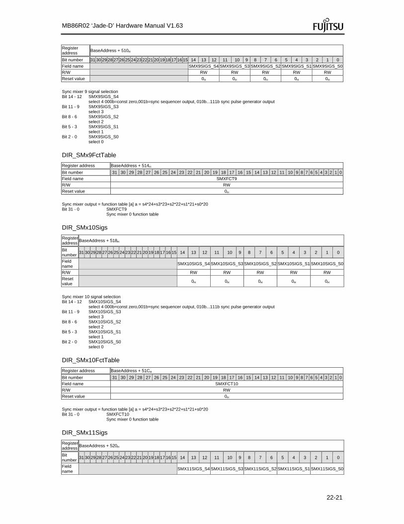
MB86R02 ‘Jade-D’ Hardware Manual V1.63
22-21
Register address
BaseAddress + 510H
Bit number 31 30 29 28 27 26 25 24 23 22 21 20 19 18 17 16 15 14 13 12 11 10 9 8 7 6 5 4 3 2 1 0
Field name SMX9SIGS_S4 SMX9SIGS_S3 SMX9SIGS_S2 SMX9SIGS_S1 SMX9SIGS_S0
R/W RW RW RW RW RW
Reset value 0H 0H 0H 0H 0H
Sync mixer 9 signal selection Bit 14 - 12 SMX9SIGS_S4
select 4 000b=const zero,001b=sync sequencer output, 010b...111b sync pulse generator output Bit 11 - 9 SMX9SIGS_S3
select 3 Bit 8 - 6 SMX9SIGS_S2
select 2 Bit 5 - 3 SMX9SIGS_S1
select 1 Bit 2 - 0 SMX9SIGS_S0
select 0
DIR_SMx9FctTable
Register address BaseAddress + 514H
Bit number 31 30 29 28 27 26 25 24 23 22 21 20 19 18 17 16 15 14 13 12 11 10 9 8 7 6 5 4 3 2 1 0
Field name SMXFCT9
R/W RW
Reset value 0H
Sync mixer output = function table [a] a = s4*24+s3*23+s2*22+s1*21+s0*20 Bit 31 - 0 SMXFCT9
Sync mixer 0 function table
DIR_SMx10Sigs
Register address
BaseAddress + 518H
Bit number
31 30 29 28 27 26 25 24 23 22 21 20 19 18 17 16 15 14 13 12 11 10 9 8 7 6 5 4 3 2 1 0
Field name
SMX10SIGS_S4 SMX10SIGS_S3 SMX10SIGS_S2 SMX10SIGS_S1 SMX10SIGS_S0
R/W RW RW RW RW RW
Reset value
0H 0H 0H 0H 0H
Sync mixer 10 signal selection Bit 14 - 12 SMX10SIGS_S4
select 4 000b=const zero,001b=sync sequencer output, 010b...111b sync pulse generator output Bit 11 - 9 SMX10SIGS_S3
select 3 Bit 8 - 6 SMX10SIGS_S2
select 2 Bit 5 - 3 SMX10SIGS_S1
select 1 Bit 2 - 0 SMX10SIGS_S0
select 0
DIR_SMx10FctTable
Register address BaseAddress + 51CH
Bit number 31 30 29 28 27 26 25 24 23 22 21 20 19 18 17 16 15 14 13 12 11 10 9 8 7 6 5 4 3 2 1 0
Field name SMXFCT10
R/W RW
Reset value 0H
Sync mixer output = function table [a] a = s4*24+s3*23+s2*22+s1*21+s0*20 Bit 31 - 0 SMXFCT10
Sync mixer 0 function table
DIR_SMx11Sigs
Register address
BaseAddress + 520H
Bit number
31 30 29 28 27 26 25 24 23 22 21 20 19 18 17 16 15 14 13 12 11 10 9 8 7 6 5 4 3 2 1 0
Field name
SMX11SIGS_S4 SMX11SIGS_S3 SMX11SIGS_S2 SMX11SIGS_S1 SMX11SIGS_S0

MB86R02 ‘Jade-D’ Hardware Manual V1.63
22-22
R/W RW RW RW RW RW
Reset value
0H 0H 0H 0H 0H
Sync mixer 11 signal selection Bit 14 - 12 SMX11SIGS_S4
select 4 000b=const zero,001b=sync sequencer output, 010b...111b sync pulse generator output Bit 11 - 9 SMX11SIGS_S3
select 3 Bit 8 - 6 SMX11SIGS_S2
select 2 Bit 5 - 3 SMX11SIGS_S1
select 1 Bit 2 - 0 SMX11SIGS_S0
select 0
DIR_SMx11FctTable
Register address BaseAddress + 524H
Bit number 31 30 29 28 27 26 25 24 23 22 21 20 19 18 17 16 15 14 13 12 11 10 9 8 7 6 5 4 3 2 1 0
Field name SMXFCT11
R/W RW
Reset value FFFFFFFFH
Sync mixer output = function table [a] a = s4*24+s3*23+s2*22+s1*21+s0*20 Bit 31 - 0 SMXFCT11
Sync mixer 0 function table
DIR_SSwitch
Register address BaseAddress + 528H
Bit number 31 30 29 28 27 26 25 24 23 22 21 20 19 18 17 16 15 14 13 12 11 10 9 8 7 6 5 4 3 2 1 0
Field name InvCtrEn SSWITCH
R/W RW RW
Reset value 0H 0H
Sync switch Bit 13 InvCtrEn
Enable for inversion control: 0b=disabled, 1b=enabled Bit 12 - 0 SSWITCH
Delay selection for all TSIG outputs including inversion control (bit 12) (0=none, 1=0.5 cycle delay of pixel clock)
DIR_RBM_CTRL
Register address BaseAddress + 52CH
Bit number 31 30 29 28 27 26 25 24 23 22 21 20 19 18 17 16 15 14 13 12 11 10 9 8 7 6 5 4 3 2 1 0
Field name ColOrder BitOrder swapoddevenbit BitPerCol IfcType Bypass
R/W RW RW RW RW RW RW
Reset value 0H 0H 0H 0H 0H 1H
RSDS Bitmap Control Bit 10 - 8
ColOrder Color Component Ordering: 000b=RGB, 001b=BRG 010b=GBR 011b=RBG 100b=GRB 101b=BGR 110b=reserved 111b=reserved
Bit 5 BitOrder Bit Order Inversion: 0b=normal order (MSB 7 downto 0), 1b=inverted order (0 upto 7 MSB)
Bit 4 swapoddevenbit ES1: Reserved, ES2: This field has only effect for ES2 and later: swap odd and even bits, 0b=no change, 1b=bit 6 and 7, 4 and 5, 2 and 3, 0 and 1 are swapped, This is needed for RSDS channel order inversion
Bit 3 BitPerCol Bits per Colour: 0b=6bits (2 LSBs are set to '0'), 1b=8bits
Bit 2 - 1
IfcType Interface protocol type: 00b=TTL, 01b=RSDS, 10b,11b=reserved
Bit 0 Bypass Bypass module: 0b=bypass disable, 1b=bypass enable
DIR_PIN0_CTRL
Register address
BaseAddress + 534H
Bit number
31 30 29 28 27 26 25 24 23 22 21 20 19 18 17 16 15 14 13 12 11 10 9 8 7 6 5 4 3 2 1 0
Field name
NChanSel0ChanSel0 NDelay0 Delay0 InOut0 NPolarity0 Polarity0 Mode0 Boost0
R/W RW RW RW RW RW RW RW RW RW
Reset value
0H 0H 0H 0H 0H 0H 0H 1H 0H

MB86R02 ‘Jade-D’ Hardware Manual V1.63
22-23
IO Module Pad 0 Control Bit 20 - 19
NChanSel0 Channel selection for N-Pin of Pad i=0 TTL: 00b=channel(i*2+1), 01b=channel(i*2), 10b=clk, 11b=const0 (TTL mode only)
Bit 18 - 17
ChanSel0 Channel selection for Pad i=0: for RSDS: 00b=channel i, 01b=reserved, 10b=clk, 11b=const0, for TTL: 00b=channel i*2, 01b=INV (from inversion control function), 10b=clk, 11b=const0
Bit 14 NDelay0 N-pin Padcell 0 delay: 0b=no delay, 1b= half bit clock cycle delay (TTL-mode only)
Bit 13 Delay0 Pad 0 delay: 0b=no delay, 1b= half bit clock cycle delay
Bit 7 InOut0 output enable control, 0b=input enabled, 1b=output enabled
Bit 6 NPolarity0 N-pin of Padcell 0 drive polarity: TTL: 0=normal, 1=inverted; RSDS: no effect
Bit 5 Polarity0 Pad 0 drive polarity: TTL :0=normal, 1=inverted; RSDS: 1=normal, 0=inverted
Bit 4 Mode0 Pad 0 drive mode: 0b=differential, 1b=TTL
Bit 1 - 0 Boost0 Boost factor for drive current: x0b=2mA, x1b=4mA (only boost[0] has effect)
DIR_PIN1_CTRL
Register address
BaseAddress + 538H
Bit number
31 30 29 28 27 26 25 24 23 22 21 20 19 18 17 16 15 14 13 12 11 10 9 8 7 6 5 4 3 2 1 0
Field name
NChanSel1ChanSel1 NDelay1 Delay1 InOut1 NPolarity1 Polarity1 Mode1 Boost1
R/W RW RW RW RW RW RW RW RW RW
Reset value
0H 0H 0H 0H 0H 0H 0H 1H 0H
IO Module Pad 1 Control Bit 20 - 19
NChanSel1 Channel selection for N-Pin of Pad i=1 TTL: 00b=channel(i*2+1), 01b=channel(i*2), 10b=clk, 11b=const0 (TTL mode only)
Bit 18 - 17
ChanSel1 Channel selection for Pad i=1: for RSDS: 00b=channel i, 01b=channel(i-1), 10b=clk, 11b=const0, for TTL : 00b=channel i*2, 01b=channel i*2-1, 10b=clk, 11b=const0
Bit 14 NDelay1 N-pin Padcell 1 delay: 0b=no delay, 1b= half bitclock cycle delay (TTL-mode only)
Bit 13 Delay1 Pad 1 delay: 0b=no delay, 1b= half bit clock cycle delay
Bit 7 InOut1 output enable control, 0b=input enabled, 1b=output enabled
Bit 6 NPolarity1 N-pin of Padcell 1 drive polarity: TTL: 0=normal, 1=inverted; RSDS: no effect
Bit 5 Polarity1 Pad 1 drive polarity: TTL: 0=normal, 1=inverted; RSDS: 1=normal, 0=inverted
Bit 4 Mode1 Pad 1 drive mode: 0b=differential, 1b=TTL
Bit 1 - 0 Boost1 Boost factor for drive current: x0b=2mA, x1b=4mA (only boost[0] has effect)
DIR_PIN2_CTRL
Register address
BaseAddress + 53CH
Bit number
31 30 29 28 27 26 25 24 23 22 21 20 19 18 17 16 15 14 13 12 11 10 9 8 7 6 5 4 3 2 1 0
Field name
NChanSel2ChanSel2 NDelay2 Delay2 InOut2 NPolarity2 Polarity2 Mode2 Boost2
R/W RW RW RW RW RW RW RW RW RW
Reset value
0H 0H 0H 0H 0H 0H 0H 1H 0H
IO Module Pad 2 Control Bit 20 - 19
NChanSel2 Channel selection for N-Pin of Pad i=2 TTL: 00b=channel(i*2+1), 01b=channel(i*2), 10b=clk, 11b=const0 (TTL mode only)
Bit 18 - 17
ChanSel2 Channel selection for Pad i=2 for RSDS: 00b=channel i, 01b=channel(i-1), 10b=clk, 11b=const0, for TTL: 00b=channel i*2, 01b=channel i*2-1, 10b=clk, 1b=const0
Bit 14 NDelay2 N-pin Padcell 2 delay: 0b=no delay, 1b= half bit clock cycle delay (TTL-mode only)
Bit 13 Delay2 Pad 2 delay: 0b=no delay, 1b= half bit clock cycle delay
Bit 7 InOut2 output enable control, 0b=input enabled, 1b=output enabled
Bit 6 NPolarity2 N-pin of Padcell 2 drive polarity: TTL: 0=normal, 1=inverted; RSDS: no effect

MB86R02 ‘Jade-D’ Hardware Manual V1.63
22-24
Bit 5 Polarity2 Pad 2 drive polarity: TTL: 0=normal, 1=inverted; RSDS: 1=normal, 0=inverted
Bit 4 Mode2 Pad 2 drive mode: 0b=differential, 1b=TTL
Bit 1 - 0 Boost2 Boost factor for drive current: x0b=2mA, x1b=4mA (only boost[0] has effect)
DIR_PIN3_CTRL
Register address
BaseAddress + 540H
Bit number
31 30 29 28 27 26 25 24 23 22 21 20 19 18 17 16 15 14 13 12 11 10 9 8 7 6 5 4 3 2 1 0
Field name
NChanSel3ChanSel3 NDelay3 Delay3 InOut3 NPolarity3 Polarity3 Mode3 Boost3
R/W RW RW RW RW RW RW RW RW RW
Reset value
0H 0H 0H 0H 0H 0H 0H 1H 0H
IO Module Pad 3 Control Bit 20 - 19
NChanSel3 Channel selection for N-Pin of Pad i=3 TTL: 00b=channel(i*2+1), 01b=channel(i*2), 10b=clk, 11b=const0 (TTL mode only)
Bit 18 - 17
ChanSel3 Channel selection for Pad i=3 for RSDS: 00b=channel i, 01b=channel(i-1), 10b=clk, 11b=const0, for TTL: 00b=channel i*2, 01b=channel i*2-1, 10b=clk, 11b=const0
Bit 14 NDelay3 N-pin Padcell 3 delay: 0b=no delay, 1b= half bit clock cycle delay (TTL-mode only)
Bit 13 Delay3 Pad 3 delay: 0b=no delay, 1b= half bit clock cycle delay
Bit 7 InOut3 output enable control, 0b=input enabled, 1b=output enabled
Bit 6 NPolarity3 N-pin of Padcell 3 drive polarity: TTL: 0=normal, 1=inverted; RSDS: no effect
Bit 5 Polarity3 Pad 3 drive polarity: TTL: 0=normal, 1=inverted; RSDS: 1=normal, 0=inverted
Bit 4 Mode3 Pad 3 drive mode: 0b=differential, 1b=TTL
Bit 1 - 0 Boost3 Boost factor for drive current: x0b=2mA, x1b=4mA (only boost[0] has effect)
DIR_PIN4_CTRL
Register address
BaseAddress + 544H
Bit number
31 30 29 28 27 26 25 24 23 22 21 20 19 18 17 16 15 14 13 12 11 10 9 8 7 6 5 4 3 2 1 0
Field name
NChanSel4ChanSel4 NDelay4 Delay4 InOut4 NPolarity4 Polarity4 Mode4 Boost4
R/W RW RW RW RW RW RW RW RW RW
Reset value
0H 0H 0H 0H 0H 0H 0H 1H 0H
IO Module Pad 4 Control Bit 20 - 19
NChanSel4 Channel selection for N-Pin of Pad i=4 TTL: 00b=channel(i*2+1), 01b=channel(i*2), 10b=clk, 11b=const0 (TTL mode only)
Bit 18 - 17
ChanSel4 Channel selection for Pad i=4 for RSDS: 00b=channel i, 01b=channel(i-1), 10b=clk, 11b=const0, for TTL: 00b=channel i*2, 01b=channel i*2-1, 10b=clk, 11b=const0
Bit 14 NDelay4 N-pin Padcell 4 delay: 0b=no delay, 1b= half bit clock cycle delay (TTL-mode only)
Bit 13 Delay4 Pad 4 delay: 0b=no delay, 1b= half bit clock cycle delay
Bit 7 InOut4 output enable control, 0b=input enabled, 1b=output enabled
Bit 6 NPolarity4 N-pin of Padcell 4 drive polarity: TTL: 0=normal, 1=inverted; RSDS: no effect
Bit 5 Polarity4 Pad 4 drive polarity: TTL: 0=normal, 1=inverted; RSDS: 1=normal, 0=inverted
Bit 4 Mode4 Pad 4 drive mode: 0b=differential, 1b=TTL
Bit 1 - 0 Boost4 Boost factor for drive current: x0b=2mA, x1b=4mA (only boost[0] has effect)
DIR_PIN5_CTRL
Register address
BaseAddress + 548H
Bit number
31 30 29 28 27 26 25 24 23 22 21 20 19 18 17 16 15 14 13 12 11 10 9 8 7 6 5 4 3 2 1 0
Field NChanSel5ChanSel5 NDelay5 Delay5 InOut5 NPolarity5 Polarity5 Mode5 Boost5

MB86R02 ‘Jade-D’ Hardware Manual V1.63
22-25
name
R/W RW RW RW RW RW RW RW RW RW
Reset value
0H 0H 0H 0H 0H 0H 0H 1H 0H
IO Module Pad 5 Control Bit 20 - 19
NChanSel5 Channel selection for N-Pin of Pad i=5 TTL: 00b=channel(i*2+1), 01b=channel(i*2), 10b=clk, 11b=const0 (TTL mode only)
Bit 18 - 17
ChanSel5 Channel selection for Pad i=5 for RSDS: 00b=channel i, 01b=channel(i-1), 10b=clk, 11b=const0, for TTL: 00b=channel i*2, 01b=channel i*2-1, 10b=clk, 11b=const0
Bit 14 NDelay5 N-pin Padcell 5 delay: 0b=no delay, 1b= half bit clock cycle delay (TTL-mode only)
Bit 13 Delay5 Pad 5 delay: 0b=no delay, 1b= half bit clock cycle delay
Bit 7 InOut5 output enable control, 0b=input enabled, 1b=output enabled
Bit 6 NPolarity5 N-pin of Padcell 5 drive polarity: TTL: 0=normal, 1=inverted; RSDS: no effect
Bit 5 Polarity5 Pad 5 drive polarity: TTL: 0=normal, 1=inverted; RSDS: 1=normal, 0=inverted
Bit 4 Mode5 Pad 5 drive mode: 0b=differential, 1b=TTL
Bit 1 - 0 Boost5 Boost factor for drive current: x0b=2mA, x1b=4mA (only boost[0] has effect)
DIR_PIN6_CTRL
Register address
BaseAddress + 54CH
Bit number
31 30 29 28 27 26 25 24 23 22 21 20 19 18 17 16 15 14 13 12 11 10 9 8 7 6 5 4 3 2 1 0
Field name
NChanSel6ChanSel6 NDelay6 Delay6 InOut6 NPolarity6 Polarity6 Mode6 Boost6
R/W RW RW RW RW RW RW RW RW RW
Reset value
0H 0H 0H 0H 0H 0H 0H 1H 0H
IO Module Pad 6 Control Bit 20 - 19
NChanSel6 Channel selection for N-Pin of Pad i=6 TTL : 00b=channel(i*2+1), 01b=channel(i*2), 10b=clk, 11b=const0 (TTL mode only)
Bit 18 - 17
ChanSel6 Channel selection for Pad i=6 for RSDS: 00b=channel i, 01b=channel(i-1), 10b=clk, 11b=const0, for TTL: 00b=channel i*2, 01b=channel i*2-1, 10b=clk, 11b=const0
Bit 14 NDelay6 N-pin Padcell 6 delay: 0b=no delay, 1b= half bit clock cycle delay (TTL-mode only)
Bit 13 Delay6 Pad 6 delay: 0b=no delay, 1b= half bit clock cycle delay
Bit 7 InOut6 output enable control, 0b=input enabled, 1b=output enabled
Bit 6 NPolarity6 N-pin of Padcell 6 drive polarity: TTL: 0=normal, 1=inverted; RSDS: no effect
Bit 5 Polarity6 Pad 6 drive polarity: TTL: 0=normal, 1=inverted; RSDS: 1=normal, 0=inverted
Bit 4 Mode6 Pad 6 drive mode: 0b=differential, 1b=TTL
Bit 1 - 0 Boost6 Boost factor for drive current: x0b=2mA, x1b=4mA (only boost[0] has effect)
DIR_PIN7_CTRL
Register address
BaseAddress + 550H
Bit number
31 30 29 28 27 26 25 24 23 22 21 20 19 18 17 16 15 14 13 12 11 10 9 8 7 6 5 4 3 2 1 0
Field name
NChanSel7ChanSel7 NDelay7 Delay7 InOut7 NPolarity7 Polarity7 Mode7 Boost7
R/W RW RW RW RW RW RW RW RW RW
Reset value
0H 0H 0H 0H 0H 0H 0H 1H 0H
IO Module Pad 7 Control Bit 20 - 19
NChanSel7 Channel selection for N-Pin of Pad i=7 TTL: 00b=channel(i*2+1), 01b=channel(i*2), 10b=clk, 11b=const0 (TTL mode only)
Bit 18 - 17
ChanSel7 Channel selection for Pad i=7 for RSDS: 00b=channel i, 01b=channel(i-1), 10b=clk, 11b=const0, for TTL: 00b=channel i*2, 01b=channel i*2-1, 10b=clk, 11b=const0
Bit 14 NDelay7 N-pin Padcell 7 delay: 0b=no delay, 1b= half bit clock cycle delay (TTL-mode only)
Bit 13 Delay7

MB86R02 ‘Jade-D’ Hardware Manual V1.63
22-26
Pad 7 delay: 0b=no delay, 1b= half bit clock cycle delay Bit 7 InOut7
output enable control, 0b=input enabled, 1b=output enabled Bit 6 NPolarity7
N-pin of Padcell 7 drive polarity: TTL: 0=normal, 1=inverted; RSDS: no effect Bit 5 Polarity7
Pad 7 drive polarity: TTL: 0=normal, 1=inverted; RSDS: 1=normal, 0=inverted Bit 4 Mode7
Pad 7 drive mode: 0b=differential, 1b=TTL Bit 1 - 0 Boost7
Boost factor for drive current: x0b=2mA, x1b=4mA (only boost[0] has effect)
DIR_PIN8_CTRL
Register address
BaseAddress + 554H
Bit number
31 30 29 28 27 26 25 24 23 22 21 20 19 18 17 16 15 14 13 12 11 10 9 8 7 6 5 4 3 2 1 0
Field name
NChanSel8ChanSel8 NDelay8 Delay8 InOut8 NPolarity8 Polarity8 Mode8 Boost8
R/W RW RW RW RW RW RW RW RW RW
Reset value
0H 0H 0H 0H 0H 0H 0H 1H 0H
IO Module Pad 8 Control Bit 20 - 19
NChanSel8 Channel selection for N-Pin of Pad i=8 TTL: 00b=channel(i*2+1), 01b=channel(i*2), 10b=clk, 11b=const0 (TTL mode only)
Bit 18 - 17
ChanSel8 Channel selection for Pad i=8 for RSDS: 00b=channel i, 01b=channel(i-1), 10b=clk, 11b=const0, for TTL: 00b=channel i*2, 01b=channel i*2-1, 10b=clk, 11b=const0
Bit 14 NDelay8 N-pin Padcell 8 delay: 0b=no delay, 1b= half bit clock cycle delay (TTL-mode only)
Bit 13 Delay8 Pad 8 delay: 0b=no delay, 1b= half bit clock cycle delay
Bit 7 InOut8 output enable control, 0b=input enabled, 1b=output enabled
Bit 6 NPolarity8 N-pin of Padcell 8 drive polarity: TTL: 0=normal, 1=inverted; RSDS: no effect
Bit 5 Polarity8 Pad 8 drive polarity: TTL: 0=normal, 1=inverted; RSDS: 1=normal, 0=inverted
Bit 4 Mode8 Pad 8 drive mode: 0b=differential, 1b=TTL
Bit 1 - 0 Boost8 Boost factor for drive current: x0b=2mA, x1b=4mA (only boost[0] has effect)
DIR_PIN9_CTRL
Register address
BaseAddress + 558H
Bit number
31 30 29 28 27 26 25 24 23 22 21 20 19 18 17 16 15 14 13 12 11 10 9 8 7 6 5 4 3 2 1 0
Field name
NChanSel9ChanSel9 NDelay9 Delay9 InOut9 NPolarity9 Polarity9 Mode9 Boost9
R/W RW RW RW RW RW RW RW RW RW
Reset value
0H 0H 0H 0H 0H 0H 0H 1H 0H
IO Module Pad 9 Control Bit 20 - 19
NChanSel9 Channel selection for N-Pin of Pad i=9 TTL: 00b=channel(i*2+1)(reserved for 6bit/color!), 01b=channel(i*2)(reserved for 6bit/color!), 10b=clk, 11b=const0 (TTL mode only)
Bit 18 - 17
ChanSel9 Channel selection for Pad i=9 for RSDS: 00b=channel i(reserved for 6bit/color!), 01b=channel(i-1), 10b=clk, 11b=const0, for TTL : 00b=channel i*2(reserved for 6bit/color!), 01b=channel i*2-1, 10b=clk, 11b=const0
Bit 14 NDelay9 N-pin Padcell 9 delay: 0b=no delay, 1b= half bit clock cycle delay (TTL-mode only)
Bit 13 Delay9 Pad 9 delay: 0b=no delay, 1b= half bit clock cycle delay
Bit 7 InOut9 output enable control, 0b=input enabled, 1b=output enabled
Bit 6 NPolarity9 N-pin of Padcell 9 drive polarity: TTL: 0=normal, 1=inverted; RSDS: no effect
Bit 5 Polarity9 Pad 9 drive polarity: TTL: 0=normal, 1=inverted; RSDS: 1=normal, 0=inverted
Bit 4 Mode9 Pad 9 drive mode: 0b=differential, 1b=TTL
Bit 1 - 0
Boost9 Boost factor for drive current: x0b=2mA, x1b=4mA (only boost[0] has effect)
DIR_PIN10_CTRL

MB86R02 ‘Jade-D’ Hardware Manual V1.63
22-27
Register address
BaseAddress + 55CH
Bit number
31 30 29 28 27 26 25 24 23 22 21 20 19 18 17 16 15 14 13 12 11 10 9 8 7 6 5 4 3 2 1 0
Field name
NChanSel10ChanSel10 NDelay10 Delay10 InOut10 NPolarity10 Polarity10 Mode10 Boost10
R/W RW RW RW RW RW RW RW RW RW
Reset value
0H 0H 0H 0H 0H 0H 0H 1H 0H
IO Module Pad 10 Control Bit 20 - 19
NChanSel10 Channel selection for N-Pin of Pad i=10 TTL: 00b=channel(i*2+1), 01b=channel(i*2), 10b=clk, 11b=const0 (TTL mode only)
Bit 18 - 17
ChanSel10 Channel selection for Pad i=10 for RSDS: 00b=channel i, 01b=channel(i-1), 10b=clk, 11b=const0, for TTL : 00b=channel i*2, 01b=channel i*2-1, 10b=clk, 11b=const0
Bit 14 NDelay10 N-pin Padcell 10 delay: 0b=no delay, 1b= half bit clock cycle delay (TTL-mode only)
Bit 13 Delay10 Pad 10 delay: 0b=no delay, 1b= half bit clock cycle delay
Bit 7 InOut10 output enable control, 0b=input enabled, 1b=output enabled
Bit 6 NPolarity10 N-pin of Padcell 10 drive polarity: TTL: 0=normal, 1=inverted; RSDS: no effect
Bit 5 Polarity10 Pad 10 drive polarity: TTL: 0=normal, 1=inverted; RSDS: 1=normal, 0=inverted
Bit 4 Mode10 Pad 10 drive mode: 0b=differential, 1b=TTL
Bit 1 - 0 Boost10 Boost factor for drive current: x0b=2mA, x1b=4mA (only boost[0] has effect)
DIR_PIN11_CTRL
Register address
BaseAddress + 560H
Bit number
31 30 29 28 27 26 25 24 23 22 21 20 19 18 17 16 15 14 13 12 11 10 9 8 7 6 5 4 3 2 1 0
Field name
NChanSel11ChanSel11 NDelay11 Delay11 InOut11 NPolarity11 Polarity11 Mode11 Boost11
R/W RW RW RW RW RW RW RW RW RW
Reset value
0H 0H 0H 0H 0H 0H 0H 1H 0H
IO Module Pad 11 Control Bit 20 - 19
NChanSel11 Channel selection for N-Pin of Pad i=11 TTL: 00b=channel(i*2+1), 01b=channel(i*2), 10b=clk, 11b=const0 (TTL mode only)
Bit 18 - 17
ChanSel11 Channel selection for Pad i=11 for RSDS: 00b=channel i, 01b=channel(i-1), 10b=clk, 11b=const0, for TTL : 00b=channel i*2, 01b=channel i*2-1, 10b=clk, 11b=const0
Bit 14 NDelay11 N-pin Padcell 11 delay: 0b=no delay, 1b= half bit clock cycle delay (TTL-mode only)
Bit 13 Delay11 Pad 11 delay: 0b=no delay, 1b= half bit clock cycle delay
Bit 7 InOut11 output enable control, 0b=input enabled, 1b=output enabled
Bit 6 NPolarity11 N-pin of Padcell 11 drive polarity: TTL: 0=normal, 1=inverted; RSDS: no effect
Bit 5 Polarity11 Pad 11 drive polarity: TTL: 0=normal, 1=inverted; RSDS: 1=normal, 0=inverted
Bit 4 Mode11 Pad 11 drive mode: 0b=differential, 1b=TTL
Bit 1 - 0 Boost11 Boost factor for drive current: x0b=2mA, x1b=4mA (only boost[0] has effect)
DIR_PIN12_CTRL
Register address
BaseAddress + 564H
Bit number
31 30 29 28 27 26 25 24 23 22 21 20 19 18 17 16 15 14 13 12 11 10 9 8 7 6 5 4 3 2 1 0
Field name
NChanSel12ChanSel12 NDelay12 Delay12 InOut12 NPolarity12 Polarity12 Mode12 Boost12
R/W RW RW RW RW RW RW RW RW RW
Reset value
0H 0H 0H 0H 0H 0H 0H 1H 0H
IO Module Pad 12 Control Bit 20 - 19
NChanSel12 Channel selection for N-Pin of Pad i=12 TTL: 00b=const0, 01b=INV (from inversion control function), 10b=clk, 11b=const0 (TTL mode

MB86R02 ‘Jade-D’ Hardware Manual V1.63
22-28
only) Bit 18 - 17
ChanSel12 Channel selection for Pad i=12 for RSDS: 00b=clk, 01b=channel(i-1), 10b=reserved, 11b=const0, for TTL: 00b=clk, 01b=channel i*2-1, 10b=INV (from inversion control function), 11b=const 0
Bit 14 NDelay12 N-pin Padcell 12 delay: 0b=no delay, 1b= half bit clock cycle delay (TTL-mode only)
Bit 13 Delay12 Pad 12 delay: 0b=no delay, 1b= half bit clock cycle delay
Bit 7 InOut12 output enable control, 0b=input enabled, 1b=output enabled
Bit 6 NPolarity12 N-pin of Padcell 12 drive polarity: TTL: 0=normal, 1=inverted; RSDS: no effect
Bit 5 Polarity12 Pad 12 drive polarity: TTL: 0=normal, 1=inverted; RSDS: 1=normal, 0=inverted
Bit 4 Mode12 Pad 12 drive mode: 0b=differential, 1b=TTL
Bit 1 - 0 Boost12 Boost factor for drive current: x0b=2mA, x1b=4mA (only boost[0] has effect)

MB86R02 ‘Jade-D’ Hardware Manual V1.63
22-29
22.5 Processing Mode
22.5.1 Processing Flow
Figure 22-2 TCON Processing Flow
22.5.2 Processing Algorithm
22.5.2.1 Operation Modes The TCON module is either active or in bypass mode (Register RBM_DIR_CTRL.bypass). In bypass mode, the RGB data from the RGB source is transmitted unchanged through the RBM submodule. Additional 3 timing signals (HSYNC, VSYNC, DE) from the frame generator are bypassed to the TSIG output signals TSIG[0:2]. The RGB data and the 3 timing signals have the same latency.

MB86R02 ‘Jade-D’ Hardware Manual V1.63
22-30
22.5.2.2 SW Reset The software reset is invoked by writing to its register. The software reset synchronizes all internal states. After power on reset the TCON module remains in this “sw reset active” state. It is deasserted by internal logic synchronous to internal video synchronization signals, that means last pixel of video frame (inclusive blanking). After configuring TCON it is therefore necessary to setup the video frame (HTP, VTP, HDP, VDP) in module DISP to provide a valid video frame to TCON module. Otherwise no RGB and display clock data is output. Configuration registers are not reseted by SW reset, only internal states of TCON.
22.5.2.3 RSDS Bitmap Mdule (RBM)
22.5.2.3.1 Block Diagram The following block diagram shows the functional design of the RBM module.
Figure 22-3 Block diagram of RBM
22.5.2.3.2 Bit Mapping RSDS 8bpc
Rising Falling
Ch0 R0 R1 Ch1 R2 R3 Ch2 R4 R5 Ch3 R6 R7 Ch4 G0 G1 Ch5 G2 G3 Ch6 G4 G5 Ch7 G6 G7 Ch8 B0 B1 Ch9 B2 B3 Ch10 B4 B5 Ch11 B6 B7
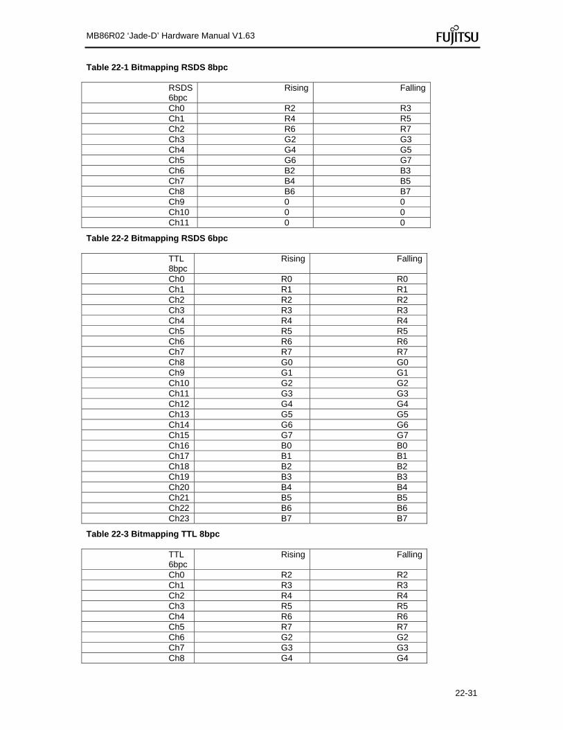
MB86R02 ‘Jade-D’ Hardware Manual V1.63
22-31
Table 22-1 Bitmapping RSDS 8bpc
RSDS 6bpc
Rising Falling
Ch0 R2 R3 Ch1 R4 R5 Ch2 R6 R7 Ch3 G2 G3 Ch4 G4 G5 Ch5 G6 G7 Ch6 B2 B3 Ch7 B4 B5 Ch8 B6 B7 Ch9 0 0 Ch10 0 0 Ch11 0 0
Table 22-2 Bitmapping RSDS 6bpc
TTL 8bpc
Rising Falling
Ch0 R0 R0 Ch1 R1 R1 Ch2 R2 R2 Ch3 R3 R3 Ch4 R4 R4 Ch5 R5 R5 Ch6 R6 R6 Ch7 R7 R7 Ch8 G0 G0 Ch9 G1 G1 Ch10 G2 G2 Ch11 G3 G3 Ch12 G4 G4 Ch13 G5 G5 Ch14 G6 G6 Ch15 G7 G7 Ch16 B0 B0 Ch17 B1 B1 Ch18 B2 B2 Ch19 B3 B3 Ch20 B4 B4 Ch21 B5 B5 Ch22 B6 B6 Ch23 B7 B7
Table 22-3 Bitmapping TTL 8bpc
TTL 6bpc
Rising Falling
Ch0 R2 R2 Ch1 R3 R3 Ch2 R4 R4 Ch3 R5 R5 Ch4 R6 R6 Ch5 R7 R7 Ch6 G2 G2 Ch7 G3 G3 Ch8 G4 G4

MB86R02 ‘Jade-D’ Hardware Manual V1.63
22-32
Ch9 G5 G5 Ch10 G6 G6 Ch11 G7 G7 Ch12 B2 B2 Ch13 B3 B3 Ch14 B4 B4 Ch15 B5 B5 Ch16 B6 B6 Ch17 B7 B7 Ch18 0 0 Ch19 0 0 Ch20 0 0 Ch21 0 0 Ch22 0 0 Ch23 0 0
Table 22-4 Bitmapping TTL 6bpc
22.5.2.4 Timing Signal Module (TSIG)
22.5.2.4.1 Block Diagram The following block diagram shows the functional design of the TSIG module (note the stages).

MB86R02 ‘Jade-D’ Hardware Manual V1.63
22-33
TSIG
SPG 0
SPG 5
···
SynSeq
Const0
SPG 6
···
SPG 11
SM 0
······
8
···
SM 6
8
SM 11
24
······
SM 5
8
Delay 0
······
Delay 6
Delay 11
······
Delay 5
···
SPG x = Sync Pulse Generator xSM x = Sync Multiplexer x
X coordinateY coordinate
Field flag
INVcontrol
TSIG5
TSIG0
TSIG6
INV
TSIG11
RGBRGB
Stage 1 Stage 2 Stage 3
Figure 22-4 Block diagram of TSIG
22.5.2.4.2 Overview Sync signals are generated using a three stage approach in order to achieve maximum flexibility. In the first stage, signals are generated which carry positional timing information. Two methods are used to create these signals. The second stage combines them to form more complex waveforms. The third stage is used to create a programmable delay of half a pixel clock cycle.
22.5.2.4.3 Position Matching One way to form the first stage signals is to use simple position matching to trigger an RS flip-flop or a toggle flip-flop. This is done using an array of twelve identical Sync Pulse Generators (SPG’s). The

MB86R02 ‘Jade-D’ Hardware Manual V1.63
22-34
following diagram shows the working principle. Note that for progressive-only systems such as 'Indigo' the bit „F“ (odd-even frame flag) must always be set to ‘0’.
Figure 22-5 Matching position with sync pulse generators TOGGLE_MODE = OFF: The output of a sync pulse generator is set or reset if the current position equals the respective programmable position in all bits for which its don’t-care-vector (which is also programmable) contains zeros. The Off matching is dominant, i.e. when both On and Off positions are matched at the same time, the output of the sync pulse generator is reset. TOGGLE_MODE = ON: The output of a sync pulse generator toggles if the current position equals the respective programmable position in all bits for which its don’t-care-vector (which is also programmable) contains zeros. Toggle mode allows e.g. frame wise toggling signals. Set/Reset overrides toggle, and if both positions match and toggle, they cancel each other out.
22.5.2.4.4 Sequence Matching A more sophisticated and powerful approach to creating first-stage signals is the use of a sequencer RAM to match a whole sequence of positions. The following diagram shows the principle of operation. A sync sequencer (SyncSeq) follows an arbitrary sequence of timing positions and generates an

MB86R02 ‘Jade-D’ Hardware Manual V1.63
22-35
appropriate output signal. The length of the sequence as well as the contents of the RAM, consisting of the position and the assigned output value are programmable.
Figure 22-6 Matching whole sequences with the Sync Sequencer Operation is as follows. To start, the address counter is reset to zero and the RAM outputs the first position that matches and the output value for this position. If the comparator signals match, the RAM address is incremented, the preset output value (bit 31) is propagated and the RAM then outputs the next position to match. This match/address increment cycle continues until the programmed sequence length is reached. If the last position is matched, the address counter is reset to zero again and the cycle starts again. It is thus possible to generate arbitrarily complex waveforms with up to 64 edges (which is the maximum sequence length).
22.5.2.4.5 Combining First Stage Sync Signals As shown above, there are twelve sync pulse generator outputs and one sync sequencer output. To obtain more complex waveforms, these signals can be combined in a second stage. Here, an array of twelve sync mixers (SMx) is used to calculate Boolean functions of first-stage signals. Each sync mixer can form any Boolean function on up to five inputs. The basic structure of one such mixer is depicted in the following diagram.

MB86R02 ‘Jade-D’ Hardware Manual V1.63
22-36
Figure 22-7 Basic structure of a Sync Mixer Basic structure of a Sync Mixer: Each of the five address lines of the 32 to 1 multiplexer can be individually selected from any of the first-stage signals. The output is the result of a table look-up. The register FctTable contains the truth table of the Boolean function calculated. The concept of the sync mixers needs some explanation. In a first step the signals to be combined are selected. These are referred to then as S0…S4 and form the address for the function table. This function table is used to look up the result of the Boolean operation the five selected signals shall be subject to. An example may help understand the topic. Assuming the outputs of three Sync Pulse Generators shall form a combined signal with the function , one would proceed as follows. At first, the Sync Mixer signals S0…S4 are assigned the Sync Pulse Generator outputs or constant zero by programming the respective multiplexers. The next step is to build the function’s truth table, as shown below. As the intended function has only three inputs, only eight entries need be specified.

MB86R02 ‘Jade-D’ Hardware Manual V1.63
22-37
Table 22-5 Function table for the Sync Mixer example It is recommended that S4…S0 are listed in order of binary number representation. This makes it possible to use the function result row directly as register contents for the Sync Mixer function table, i.e. the last row is interpreted as binary 32 bit number with the LSB in the first row and the MSB in the last. For the example this would be [xxxx xxxx xxxx xxxx xxxx xxxx 0000 1000] binary, with x’s denoting arbitrarily set or reset bits, since these will never be read out of the function table.
22.5.2.4.6 Sync Signal Delay Adjustment Before the outputs of the twelve Sync Mixers are connected to actual GDC pins, they are fed through a programmable delay stage. This allows the signals either to be left untouched or delayed for half a pixel clock cycle. This delay can be set for each of the twelve Sync Mixer output signals individually with the Sync Switch register.
22.5.2.5 Inversion Signal Generation The purpose of the inversion signal INV is the minimization of total signal edge transitions on the RGB data bus. Especially for TTL RGB signals this brings benefits for EMI. The inversion signal is transmitted as accompanying signal to the output RGB data signals. The input data of time (n - 1) is compared to the data at time n. If more than the half of the active RGB bits have a transition from low to high or vice versa, then INV toggles between HIGH and LOW. When INV is output as HIGH, all the bits of the current pixel are inverted.

MB86R02 ‘Jade-D’ Hardware Manual V1.63
22-38
22.5.2.6 Bypass-Mode
22.5.2.6.1 Pin mapping “Bypass Mode Data”
Figure 22-8 Pin Mapping Bypass Mode data
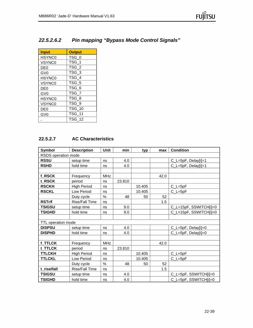
MB86R02 ‘Jade-D’ Hardware Manual V1.63
22-39
22.5.2.6.2 Pin mapping “Bypass Mode Control Signals”
Input Output HSYNC0 TSG_0 VSYNC0 TSG_1
DE0 TSG_2
GV0 TSG_3
HSYNC0 TSG_4
VSYNC0 TSG_5
DE0 TSG_6
GV0 TSG_7
HSYNC0 TSG_8
VSYNC0 TSG_9
DE0 TSG_10
GV0 TSG_11
- TSG_12
22.5.2.7 AC Characteristics Symbol Description Unit min typ max Condition RSDS operation mode RSSU setup time ns 4.0 C_L=5pF, Delay[i]=1 RSHD hold time ns 4.0 C_L=5pF, Delay[i]=1 f_RSCK Frequency MHz 42.0 t_RSCK period ns 23.810 RSCKH High Period ns 10.405 C_L=5pF RSCKL Low Period ns 10.405 C_L=5pF Duty cycle % 48 50 52 RSTr/f Rise/Fall Time ns 1.5 TSIGSU setup time ns 9.0 C_L=15pF, SSWITCH[i]=0 TSIGHD hold time ns 9.0 C_L=15pF, SSWITCH[i]=0 TTL operation mode DISPSU setup time ns 4.0 C_L=5pF, Delay[i]=0 DISPHD hold time ns 4.0 C_L=5pF, Delay[i]=0 f_TTLCK Frequency MHz 42.0 t_TTLCK period ns 23.810 TTLCKH High Period ns 10.405 C_L=5pF TTLCKL Low Period ns 10.405 C_L=5pF Duty cycle % 48 50 52 t_rise/fall Rise/Fall Time ns 1.5 TSIGSU setup time ns 4.0 C_L=5pF, SSWITCH[i]=0 TSIGHD hold time ns 4.0 C_L=5pF, SSWITCH[i]=0

MB86R02 ‘Jade-D’ Hardware Manual V1.63
22-40
Figure 22-9 RSDS operation Output Timing
Figure 22-10 Rise Fall Times

MB86R02 ‘Jade-D’ Hardware Manual V1.63
22-41
Figure 22-11 TTL operation output timing (1)
TTLCKH TTLCKL
50%
TTLDAT (pins DISP[i])Registers DIR_Pin_ctrl[i].Delay=0
DISPHDDISPSU
Pins TSIG[i]Register Dir_SSwitch.SSwitch =0
TSIGHDTSIGSU
TTLCK (pin DISP[j])Register DIR_Pin_ctrl[j].Delay=0
Register DIR_Pin_Ctrl[j].Polarity=1
Figure 22-12 TTL operation output timing (2)
22.5.3 Limitations
Several configuration registers only have an effect with TTL-mode enabled. These registers are marked “TTL-mode only”.
Reprogramming of configuration registers during active display can cause undefined effects.
Only word access is supported for the address range 0h … 0FFh (embedded memory). Byte
or halfword access is not allowed to this address range. All the other addresses support byte, halfword, word access.

MB86R02 ‘Jade-D’ Hardware Manual V1.63
22-42
22.6 Application Note
22.6.1.1 Channel to pin mapping
22.6.1.2 Pin mapping RSDS In RSDS mode each IO-cell can be used for clock distribution. The table below shows possible positions for clock output of a 24 bit RGB panel Interface. For 18bit interfaces only cell0 to 9 is available. Programming is done by register DIR_PIN[i]_CTRL.(N)channel_sel[i].
Table 22-6
clock position (RSDS)
cell pin 0 1 2 3 4 5 6 7 8 9 10 11 12
0 d clk 0/1 0/1 0/1 0/1 0/1 0/1 0/1 0/1 0/1 0/1 0/1 0/1
1 d 0/1 clk 2/3 2/3 2/3 2/3 2/3 2/3 2/3 2/3 2/3 2/3 2/3
2 d 2/3 2/3 clk 4/5 4/5 4/5 4/5 4/5 4/5 4/5 4/5 4/5 4/5
3 d 4/5 4/5 4/5 clk 6/7 6/7 6/7 6/7 6/7 6/7 6/7 6/7 6/7
4 d 6/7 6/7 6/7 6/7 clk 8/9 8/9 8/9 8/9 8/9 8/9 8/9 8/9
5 d 8/9 8/9 8/9 8/9 8/9 clk 10/11 10/11 10/11 10/11 10/11 10/11 10/11
6 d 10/11 10/11 10/11 10/11 10/11 10/11 clk 12/13 12/13 12/13 12/13 12/13 12/13
7 d 12/13 12/13 12/13 12/13 12/13 12/13 12/13 clk 14/15 14/15 14/15 14/15 14/15
8 d 12/13 12/13 12/13 12/13 12/13 12/13 12/13 12/13 clk 16/17 16/17 16/17 16/17
9 d 14/15 14/15 14/15 14/15 14/15 14/15 14/15 14/15 14/15 clk 18/19 18/19 18/19
10 d 18/19 18/19 18/19 18/19 18/19 18/19 18/19 18/19 18/19 18/19 clk 20/21 20/21
11 d 20/21 20/21 20/21 20/21 20/21 20/21 20/21 20/21 20/21 20/21 20/21 clk 22/23
12 d 22/23 22/23 22/23 22/23 22/23 22/23 22/23 22/23 22/23 22/23 22/23 22/23 clk
22.6.1.3 Pin mapping TTL In single-ended TTL mode, each of the 24 output pins can be used for clock distribution. Table 22-8 visualizes possible rationable settings for a 24 bit output data plus clock to single-ended I/O cells, which can be programmed by registers DIR_PIN[i]_CTRL.(N)channel_sel[i].
Table 22-9 visualizes possible rationable settings for a 18 bit output data plus clock to single-ended I/O cells, which can be programmed by registers DIR_PIN[i]_CTRL.(N)channel_sel[i].
Pads can be configured to contribute two clock sources (this allows at the board to combine these two clock signals to achieve a higher drive strength if necessary, see Figure 22-10) or to contribute one clock source and one inversion control signal “INV” on different pins shown in the table below. Remark: In case of integration within systems with only 10 pad cells ( e.g. an Indigo GDC) color channel 18 is provided but not needed. So it makes sense to use cell 9 pin a1 for clk.
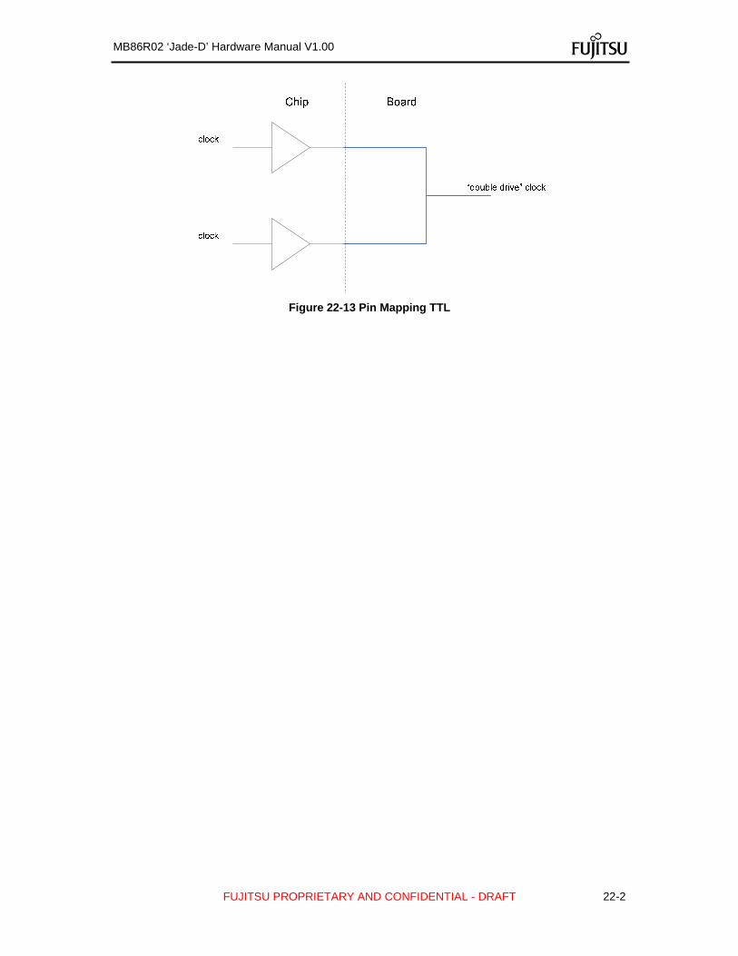
MB86R02 ‘Jade-D’ Hardware Manual V1.00
FUJITSU PROPRIETARY AND CONFIDENTIAL - DRAFT
22-2
Figure 22-13 Pin Mapping TTL

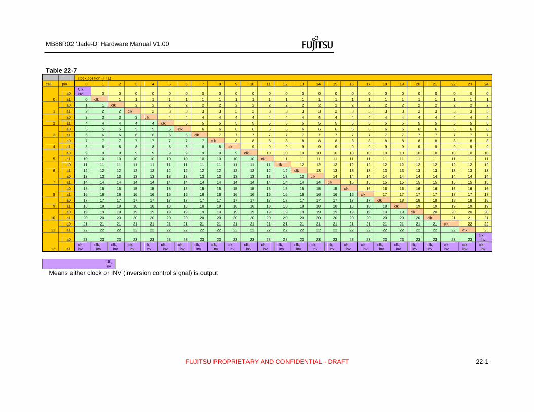
MB86R02 ‘Jade-D’ Hardware Manual V1.00
FUJITSU PROPRIETARY AND CONFIDENTIAL - DRAFT
22-1
Table 22-7 clock position (TTL)
cell pin 0 1 2 3 4 5 6 7 8 9 10 11 12 13 14 15 16 17 18 19 20 21 22 23 24
0
a0 Clk, invl 0 0 0 0 0 0 0 0 0 0 0 0 0 0 0 0 0 0 0 0 0 0 0 0
a1 0 clk 1 1 1 1 1 1 1 1 1 1 1 1 1 1 1 1 1 1 1 1 1 1 1
1
a0 1 1 clk 2 2 2 2 2 2 2 2 2 2 2 2 2 2 2 2 2 2 2 2 2 2
a1 2 2 2 clk 3 3 3 3 3 3 3 3 3 3 3 3 3 3 3 3 3 3 3 3 3
2
a0 3 3 3 3 clk 4 4 4 4 4 4 4 4 4 4 4 4 4 4 4 4 4 4 4 4
a1 4 4 4 4 4 clk 5 5 5 5 5 5 5 5 5 5 5 5 5 5 5 5 5 5 5
3
a0 5 5 5 5 5 5 clk 6 6 6 6 6 6 6 6 6 6 6 6 6 6 6 6 6 6
a1 6 6 6 6 6 6 6 clk 7 7 7 7 7 7 7 7 7 7 7 7 7 7 7 7 7
4
a0 7 7 7 7 7 7 7 7 clk 8 8 8 8 8 8 8 8 8 8 8 8 8 8 8 8
a1 8 8 8 8 8 8 8 8 8 clk 9 9 9 9 9 9 9 9 9 9 9 9 9 9 9
5
a0 9 9 9 9 9 9 9 9 9 9 clk 10 10 10 10 10 10 10 10 10 10 10 10 10 10
a1 10 10 10 10 10 10 10 10 10 10 10 clk 11 11 11 11 11 11 11 11 11 11 11 11 11
6
a0 11 11 11 11 11 11 11 11 11 11 11 11 clk 12 12 12 12 12 12 12 12 12 12 12 12
a1 12 12 12 12 12 12 12 12 12 12 12 12 12 clk 13 13 13 13 13 13 13 13 13 13 13
7
a0 13 13 13 13 13 13 13 13 13 13 13 13 13 13 clk 14 14 14 14 14 14 14 14 14 14
a1 14 14 14 14 14 14 14 14 14 14 14 14 14 14 14 clk 15 15 15 15 15 15 15 15 15
8
a0 15 15 15 15 15 15 15 15 15 15 15 15 15 15 15 15 clk 16 16 16 16 16 16 16 16
a1 16 16 16 16 16 16 16 16 16 16 16 16 16 16 16 16 16 clk 17 17 17 17 17 17 17
9
a0 17 17 17 17 17 17 17 17 17 17 17 17 17 17 17 17 17 17 clk 18 18 18 18 18 18
a1 18 18 18 18 18 18 18 18 18 18 18 18 18 18 18 18 18 18 18 clk 19 19 19 19 19
10
a0 19 19 19 19 19 19 19 19 19 19 19 19 19 19 19 19 19 19 19 19 clk 20 20 20 20
a1 20 20 20 20 20 20 20 20 20 20 20 20 20 20 20 20 20 20 20 20 20 clk 21 21 21
11
a0 21 21 21 21 21 21 21 21 21 21 21 21 21 21 21 21 21 21 21 21 21 21 clk 22 22
a1 22 22 22 22 22 22 22 22 22 22 22 22 22 22 22 22 22 22 22 22 22 22 22 clk 23
12
a0 23 23 23 23 23 23 23 23 23 23 23 23 23 23 23 23 23 23 23 23 23 23 23 23 clk, inv
a1 clk, inv
clk, inv
clk, inv
clk, inv
clk, inv
clk, inv
clk, inv
clk, inv
clk, inv
clk, inv
clk, inv
clk, inv
clk, inv
clk, inv
clk, inv
clk, inv
clk, inv
clk, inv
clk, inv
clk, inv
clk, inv
clk, inv
clk, inv
clk inv
clk, inv
clk, inv
Means either clock or INV (inversion control signal) is output


22-1
MB86R02 ‘Jade-D’ Hardware Manual V1.00
FUJITSU PROPRIETARY AND CONFIDENTIAL
Table 22-8 clock position (TTL)
cell pinn 0 1 2 3 4 5 6 7 8 9 10 11 12 13 14 15 16 17 18 18&19 19 + INV
0
a0 clk 0 0 0 0 0 0 0 0 0 0 0 0 0 0 0 0 0 0 0 inv
a1 0 clk 1 1 1 1 1 1 1 1 1 1 1 1 1 1 1 1 1 1 0
1
a0 1 1 clk 2 2 2 2 2 2 2 2 2 2 2 2 2 2 2 2 2 1
a1 2 2 2 clk 3 3 3 3 3 3 3 3 3 3 3 3 3 3 3 3 2
2
a0 3 3 3 3 clk 4 4 4 4 4 4 4 4 4 4 4 4 4 4 4 3
a1 4 4 4 4 4 clk 5 5 5 5 5 5 5 5 5 5 5 5 5 5 4
3
a0 5 5 5 5 5 5 clk 6 6 6 6 6 6 6 6 6 6 6 6 6 5
a1 6 6 6 6 6 6 6 clk 7 7 7 7 7 7 7 7 7 7 7 7 6
4
a0 7 7 7 7 7 7 7 7 clk 8 8 8 8 8 8 8 8 8 8 8 7
a1 8 8 8 8 8 8 8 8 8 clk 9 9 9 9 9 9 9 9 9 9 8
5
a0 9 9 9 9 9 9 9 9 9 9 clk 10 10 10 10 10 10 10 10 10 9
a1 10 10 10 10 10 10 10 10 10 10 10 clk 11 11 11 11 11 11 11 11 10
6
a0 11 11 11 11 11 11 11 11 11 11 11 11 clk 12 12 12 12 12 12 12 11
a1 12 12 12 12 12 12 12 12 12 12 12 12 12 clk 13 13 13 13 13 13 12
7
a0 13 13 13 13 13 13 13 13 13 13 13 13 13 13 clk 14 14 14 14 14 13
a1 14 14 14 14 14 14 14 14 14 14 14 14 14 14 14 clk 15 15 15 15 14
8
a0 15 15 15 15 15 15 15 15 15 15 15 15 15 15 15 15 clk 16 16 16 15
a1 16 16 16 16 16 16 16 16 16 16 16 16 16 16 16 16 16 clk 17 17 16
9
a0 17 17 17 17 17 17 17 17 17 17 17 17 17 17 17 17 17 17 clk clk 17
a1 Const0 Const0 Const0 Const0 Const0 Const0 Const0 Const0 Const0 Const0 Const0 Const0 Const0 Const0 Const0 Const0 Const0 Const0 Const0 clk clk

22-2
MB86R02 ‘Jade-D’ Hardware Manual V1.00
FUJITSU PROPRIETARY AND CONFIDENTIAL

22-1
MB86R02 ‘Jade-D’ Hardware Manual V1.00
FUJITSU PROPRIETARY AND CONFIDENTIAL
22.6.2 Example Control Flow The following diagram shows the decision flow and configuration steps for a panel driver routine in principle. Of course a lot of panel timing relevant parameters are configured at the DISP module. This is not covered in this section. Some decisions must already be taken when designing the board, selecting the used panel, driver ICs, etc. The diagram does not show the detailed flow and exact order of configuration steps for one application.
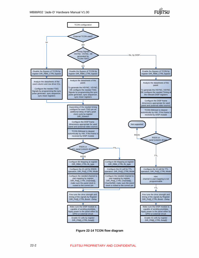
22-2
MB86R02 ‘Jade-D’ Hardware Manual V1.00
FUJITSU PROPRIETARY AND CONFIDENTIAL
TCON configuration
Timing Signals HSYNC. VSYNC, DE
generated by TCON-TSIG?
yes
No, by DISP
External TCON used?
yesno
Configure the DISP frame dimensions appropriate for used panel and (external video source)
Analyze the datasheets of the used column and row driver ICs.
Configure the needed TSIG Signals by programming the sync pulse generator, sync sequencer,
sync mixer registers
Configure the needed channel to pad mapping by register
DIR_Pin[i]_CTRL.ChanSel[i], make sure the panel clock is
routed to the correct pin
Configure Bit Mapping at register DIR_RBM_CTRL.Ifc_type
TCON-SWreset is cleared automtically by HW, if first frame is
received by DISP module
RSDS or TTL panel (column driver)
TTL
RSDS
Disable the Bypass of TCON by register DIR_RBM_CTRL.bypass
Configure the IO cell for RSDS operation, DIR_Pin[i]_CTRL.Mode
Fine tune the drive strength and timing of the signals by Register DIR_Pin[i]_CTRL.Boost -.Delay
Make sure the DISP module is capable of sending pixeldata,
Apply power to the panel either by GPIO or external circuit.
Analyze the datasheets of the panel.
To generate the HSYNC, VSYNC, DE configure the needed TSIG
Signals by programming the sync pulse generator, sync sequencer,
sync mixer registers
Depending of the needed timing configure for each TSIG pin an additional delay of half a pixel
clock cycle by register DIR_SSwitch
Disable the Bypass of TCON by register DIR_RBM_CTRL.bypass
Enable the Bypass of TCON by register DIR_RBM_CTRL.bypass
Analyze the datasheets of the panel.
To generate the HSYNC, VSYNC, DE configure the needed Timing at
the relevant DISP registers
Configure Bit Mapping at register DIR_RBM_CTRL.Ifc_type
Configure the needed channel to pad mapping by register
DIR_Pin[i]_CTRL.ChanSel[i], -ChanSelN[i], make sure the panel clock is routed to the correct pin
Configure the IO cell for TTL operation, DIR_Pin[i]_CTRL.Mode
Enable IO cells by register DIR_PIN[i]_CTRL.Susp[i]
RSDS or TTL panel (column driver)
TTL
RSDS
Not supported
Configure the DISP frame dimensions appropriate for used panel and (external video source)
TCON-SWreset is cleared automtically by HW, if first frame is
received by DISP module
Configure the IO cell for TTL operation, DIR_Pin[i]_CTRL.Mode
TTL
Enable IO cells by register DIR_PIN[i]_CTRL.Susp[i]
Make sure the DISP module is capable of sending pixeldata,
Apply power to the panel either by GPIO or external circuit.
Fine tune the drive strength and timing of the signals by Register DIR_Pin[i]_CTRL.Boost -.Delay
Hint:channel to pad mapping is not
programmable
Figure 22-14 TCON flow diagram

MB86R02 ‘Jade-D’ Hardware Manual V1.63
23-1
23 Run-Length Decompression (RLD)
23.1 Position of Block in whole LSI
Figure 23-1 Location of the RLD unit in the GDC
23.1.1 Data Flow in the LSI
Figure 23-2 Example position in LSI
Phase 1 HDMAC initiates a transfer form CCBP to RLD. Data will be latched into HDMAC’s FIFO Phase2 HDMAC prompts FIFO data to input FIFO of RLD Phase3 RLD decompresses the FIFO data and transfers them to Target destination
MB86R02 ‘Jade-D’ Hardware Manual V1.63
23-2
23.2 Overview The Run-Length Decompression Unit (RLD) allows the unpacking of run-length compressed data without processor interaction purely in hardware. For data in flash memory, such as simple graphic content e.g. pictograms, company images (logo) etc., run-length decoding brings a substantial benefit for bandwidth saving on the used external bus system especially during a setup phase. The precondition for relieving a processor is that the input data is conform with the data format and organization required by the target location (e.g. video RAM, sprite pattern RAM), so that no further reformatting is necessary. The RLD unit consists of a decompression module, an AHB slave, used for configuration data and compressed data input and an AHB master for decompressed data output. This allows the decompressing of data delivered by arbitrary AHB modules in the system. Also the target location may be an arbitrary AHB slave of the system.
23.3 Feature List
Support of a simple run length compressing format (TGA™ like format, see also Fujitsu’s MB87P2020A 'Jasmine' Hardware Manual)
1/2/4/8/16/24/32 bit per pixel formats supported
AHB master for data output
FIFO for data input and output, allows burst access of AHB
23.3.1 References Truevision™ TGA™ FILE FORMAT SPECIFICATION, Truevision Inc.Version 2.0
23.3.2 Integration and Application Hints 23.3.2.1 Usage of RLD with Jade-D The transfer of data from an arbitrary input interface like MEMC is controlled by the central MB86R02 'JADE-D' AHB HDMA module, while the transfer of data from MediaLB to RLD is controlled by MediaLB itself. The transfer of the decompressed output data from RLD to the wished target location like the video memory in the external DRAM is controlled by the local RLD DMA controller.
23.4 Communication Protocols (Timing Diagrams)
23.4.1 Result Interface The standard AHB-Bus communication protocol is used.
23.4.2 Configuration Bus Interface The standard AHB-Bus communication protocol is used.
23.4.3 Interrupt The RLD unit has a level interrupt output signal
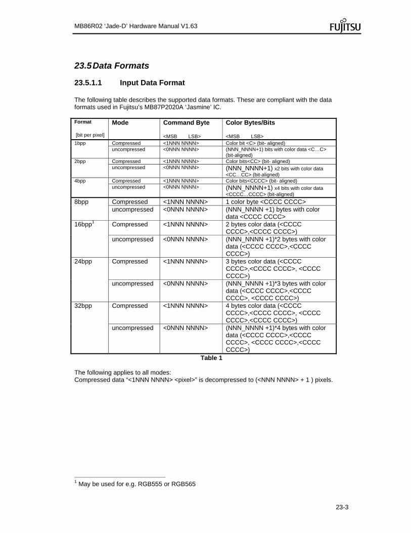
MB86R02 ‘Jade-D’ Hardware Manual V1.63
23-3
23.5 Data Formats
23.5.1.1 Input Data Format The following table describes the supported data formats. These are compliant with the data formats used in Fujitsu’s MB87P2020A ‘Jasmine’ IC. Format [bit per pixel]
Mode Command Byte <MSB LSB>
Color Bytes/Bits <MSB LSB>
1bpp Compressed <1NNN NNNN> Color bit <C> (bit- aligned)uncompressed <0NNN NNNN> (NNN_NNNN+1) bits with color data <C…C>
(bit-aligned)2bpp Compressed <1NNN NNNN> Color bits<CC> (bit- aligned)
uncompressed <0NNN NNNN> (NNN_NNNN+1) x2 bits with color data <CC…CC> (bit-aligned)
4bpp Compressed <1NNN NNNN> Color bits<CCCC> (bit- aligned) uncompressed <0NNN NNNN> (NNN_NNNN+1) x4 bits with color data
<CCCC…CCCC> (bit-aligned) 8bpp Compressed <1NNN NNNN> 1 color byte <CCCC CCCC>
uncompressed <0NNN NNNN> (NNN_NNNN +1) bytes with color data <CCCC CCCC>
16bpp1 Compressed <1NNN NNNN> 2 bytes color data (<CCCC CCCC>,<CCCC CCCC>)
uncompressed <0NNN NNNN> (NNN_NNNN +1)*2 bytes with color data (<CCCC CCCC>,<CCCC CCCC>)
24bpp Compressed <1NNN NNNN> 3 bytes color data (<CCCC CCCC>,<CCCC CCCC>, <CCCC CCCC>)
uncompressed <0NNN NNNN> (NNN_NNNN +1)*3 bytes with color data (<CCCC CCCC>,<CCCC CCCC>, <CCCC CCCC>)
32bpp Compressed <1NNN NNNN> 4 bytes color data (<CCCC CCCC>,<CCCC CCCC>, <CCCC CCCC>,<CCCC CCCC>)
uncompressed <0NNN NNNN> (NNN_NNNN +1)*4 bytes with color data (<CCCC CCCC>,<CCCC CCCC>, <CCCC CCCC>,<CCCC CCCC>)
Table 1 The following applies to all modes: Compressed data “<1NNN NNNN> <pixel>” is decompressed to (<NNN NNNN> + 1 ) pixels.
1 May be used for e.g. RGB555 or RGB565

MB86R02 ‘Jade-D’ Hardware Manual V1.63
23-4
Figure 23-3 Example for uncompressed data input RGB888
Figure 23-4 Example for compressed data input RGB888
23.5.1.2 Output Data Format Output data format depends on the selected BPP (bit per pixel) format. Further bit/word alignment, memory stride calculation is supported in hardware. The output data is organized as Big Endian.
23.6 Software Interface
23.6.1 Format of Register Description The register descriptions in the following sections use the format shown below to describe each bit field of a register. Register address Offset
Bit number 31 30 29 28 27 26 25 24 23 22 21 20 19 18 17 16 15 14 13 12 11 10 9 8 7 6 5 4 3 2 1 0
Field name
R/W
Reset value
Meaning of items and sign

MB86R02 ‘Jade-D’ Hardware Manual V1.63
23-5
Register address Register address shows the address (Offset address) of the register.
Bit number Bit number shows bit position of the register.
Field name Field name shows bit name of the register.
R/W R/W shows the read/write attribute of each bit field: R: Read W: Write W1C: Writing a value of "1" clears the register.
Reset value Reset value indicates the value of each bit field immediately after reset. 0: Initial value is "0". 1: Initial value is "1". X: Undefined.
Unused register fields are marked with a solid grey background. Bit vectors are unsigned integers, if nothing else specified.
23.6.2 Global Address For the module base address, please refer to the global address map of this manual.
23.6.3 Register Summary
Address Register Name DescriptionBase address + 0H SWReset SW reset Base address + 4H RldCfg general configuration register Base address + 8H StrideCfg0 Stride general configuration register Base address + CH StrideCfg1 Line / Stride Length
Base address + 10H
BYTECNT Target number of decompressed bytes
Base address + 14H
OFIFO Output FIFO Control
Base address + 18H
DestAddress Local AHB-master transfer Destination address
Base address + 1CH
AHBMCtrl Local AHB-master transfer Configuration/Control
Base address + 20H
RLDCtrl General Control
Base address + 24H
IEN Interrupt Enable register
Base address + 28H
ISTS Interrupt status flags, a '1' signifies that the corresponding interrupt condition occurred (even if interrupt is disabled), write '1' clears the flag,
Base address + 2CH
Status Status register
Base address + 30H
SAHBData AHB Slave Input Data
Base address + 34H
TransferCount Local AHB-master transfer count
Base address + 38H
CurAddress Local AHB-master transfer Current address

MB86R02 ‘Jade-D’ Hardware Manual V1.63
23-6
23.6.4 Register Description SWReset
Register address BaseAddress + 0H
Bit number 31 30 29 28 27 26 25 24 23 22 21 20 19 18 17 16 15 14 13 12 11 10 9 8 7 6 5 4 3 2 1 0
Field name SWReset
R/W RW
Reset value 0H
SW reset Bit 0 SWReset
sw reset (flush all FIFOs)
RldCfg
Register address BaseAddress + 4H
Bit number 31 30 29 28 27 26 25 24 23 22 21 20 19 18 17 16 15 14 13 12 11 10 9 8 7 6 5 4 3 2 1 0
Field name AlignMode BPP
R/W RW RW
Reset value 0H 0H
general configuration register Bit 8 AlignMode
output data format 0b=bit alligned output 1b=word (32bit) alligned output Bit 2 - 0 BPP
Bit per pixel, 000b=1, 001b=2, 010b=4, 011b=8, 100b=16, 101b=24, 110b=32 others=reserved
StrideCfg0
Register address BaseAddress + 8H
Bit number 31 30 29 28 27 26 25 24 23 22 21 20 19 18 17 16 15 14 13 12 11 10 9 8 7 6 5 4 3 2 1 0
Field name StrideEn
R/W RW
Reset value 0H
Stride general configuration register Bit 0 StrideEn
Enable for output data stride alligned, 0b=disabled (no observation of LineLength and Stride, needed for 4x4 1bpp sprites), 1b=enabled
StrideCfg1
Register address BaseAddress + CH
Bit number 31 30 29 28 27 26 25 24 23 22 21 20 19 18 17 16 15 14 13 12 11 10 9 8 7 6 5 4 3 2 1 0
Field name Stride LineLength
R/W RW RW
Reset value 0H 0H
Line / Stride Length Bit 31 - 16 Stride
Stride: number of byte -1 (must to be 4byte aligned) Bit 13 - 0 LineLength
number of bytes per line - 1 (must to be 4byte aligned)
BYTECNT
Register address BaseAddress + 10H
Bit number 31 30 29 28 27 26 25 24 23 22 21 20 19 18 17 16 15 14 13 12 11 10 9 8 7 6 5 4 3 2 1 0
Field name ByteCnt
R/W RW
Reset value 0H
Target number of decompressed bytes Bit 31 - 0 ByteCnt
Target number of decompressed bytes
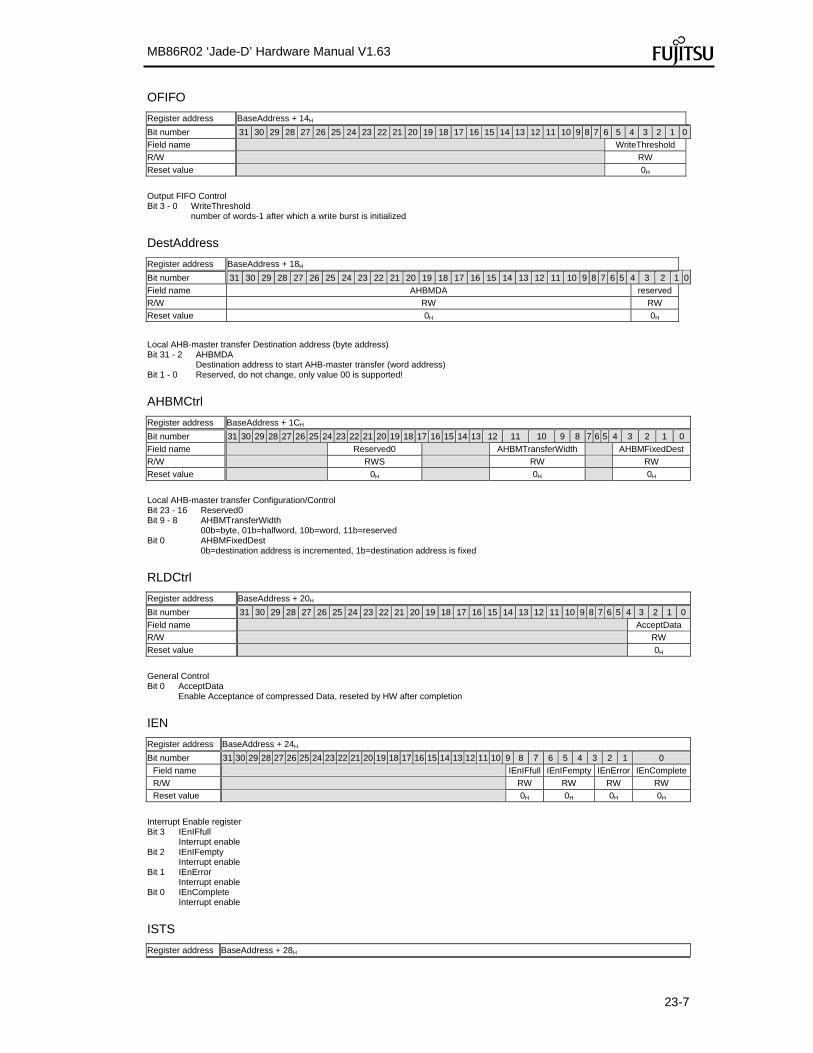
MB86R02 ‘Jade-D’ Hardware Manual V1.63
23-7
OFIFO
Register address BaseAddress + 14H
Bit number 31 30 29 28 27 26 25 24 23 22 21 20 19 18 17 16 15 14 13 12 11 10 9 8 7 6 5 4 3 2 1 0
Field name WriteThreshold
R/W RW
Reset value 0H
Output FIFO Control Bit 3 - 0 WriteThreshold
number of words-1 after which a write burst is initialized
DestAddress
Register address BaseAddress + 18H
Bit number 31 30 29 28 27 26 25 24 23 22 21 20 19 18 17 16 15 14 13 12 11 10 9 8 7 6 5 4 3 2 1 0
Field name AHBMDA reserved
R/W RW RW
Reset value 0H 0H
Local AHB-master transfer Destination address (byte address) Bit 31 - 2 AHBMDA
Destination address to start AHB-master transfer (word address) Bit 1 - 0 Reserved, do not change, only value 00 is supported!
AHBMCtrl
Register address BaseAddress + 1CH
Bit number 31 30 29 28 27 26 25 24 23 22 21 20 19 18 17 16 15 14 13 12 11 10 9 8 7 6 5 4 3 2 1 0
Field name Reserved0 AHBMTransferWidth AHBMFixedDest
R/W RWS RW RW
Reset value 0H 0H 0H
Local AHB-master transfer Configuration/Control Bit 23 - 16 Reserved0 Bit 9 - 8 AHBMTransferWidth
00b=byte, 01b=halfword, 10b=word, 11b=reserved Bit 0 AHBMFixedDest
0b=destination address is incremented, 1b=destination address is fixed
RLDCtrl
Register address BaseAddress + 20H
Bit number 31 30 29 28 27 26 25 24 23 22 21 20 19 18 17 16 15 14 13 12 11 10 9 8 7 6 5 4 3 2 1 0
Field name AcceptData
R/W RW
Reset value 0H
General Control Bit 0 AcceptData
Enable Acceptance of compressed Data, reseted by HW after completion
IEN
Register address BaseAddress + 24H
Bit number 31 30 29 28 27 26 25 24 23 22 21 20 19 18 17 16 15 14 13 12 11 10 9 8 7 6 5 4 3 2 1 0
Field name IEnIFfull IEnIFempty IEnError IEnComplete
R/W RW RW RW RW
Reset value 0H 0H 0H 0H
Interrupt Enable register Bit 3 IEnIFfull
Interrupt enable Bit 2 IEnIFempty
Interrupt enable Bit 1 IEnError
Interrupt enable Bit 0 IEnComplete
Interrupt enable
ISTS
Register address BaseAddress + 28H

MB86R02 ‘Jade-D’ Hardware Manual V1.63
23-8
Bit number 31 30 29 28 27 26 25 24 23 22 21 20 19 18 17 16 15 14 13 12 11 10 9 8 7 6 5 4 3 2 1 0
Field name IStsIFfull IStsIFempty IStsError IStsComplete
R/W RW RW RW RW
Reset value 0H 0H 0H 0H
Interrupt status flags, a '1' signifies that the corresponding interrupt condition occurred (even if interrupt is disabled), write '1' clears the flag, Bit 3 IStsIFfull
Interrupt Status for condition Input FIFO full Bit 2 IStsIFempty
Interrupt Status for condition Input FIFO empty Bit 1 IStsError
Interrupt Status for condition AHB Destination access error (info from AHB HRESP) Bit 0 IStsComplete
Interrupt Status for Condition RLD complete (Target Byte Count reached)
Status
Register address BaseAddress + 2CH
Bit number 31 30 29 28 27 26 25 24 23 22 21 20 19 18 17 16 15 14 13 12 11 10 9 8 7 6 5 4 3 2 1 0
Field name Reserved IFIFOempty OFIFOfull IFIFOfull Busy
R/W RWS R R R R
Reset value 0 1 0 0 0
Status register Bit 4 Reserved Bit 3 IFIFOempty
Input FIFO currently empty Bit 2 OFIFOfull
Output FIFO currently full Bit 1 IFIFOfull
Input FIFO currently full Bit 0 Busy
RLD busy
SAHBData
Register address BaseAddress + 30H
Bit number 31 30 29 28 27 26 25 24 23 22 21 20 19 18 17 16 15 14 13 12 11 10 9 8 7 6 5 4 3 2 1 0
Field name InData
R/W RW
Reset value 0H
AHB Slave Input Data Bit 31 - 0 InData
RLD input data (Data written at this address is is latched into the RLD IFIFO) Hint: Data is only accepted if register RLDCtrl.AcceptData = 1
TransferCount
Register address BaseAddress + 34H
Bit number 31 30 29 28 27 26 25 24 23 22 21 20 19 18 17 16 15 14 13 12 11 10 9 8 7 6 5 4 3 2 1 0
Field name AHBMTransferCount
R/W R
Reset value 0H
Local AHB-master transfer count Bit 31 - 0 AHBMTransferCount
status count of remaining bytes to transfer during current transaction (decrementing counter)
CurAddress
Register address BaseAddress + 38H
Bit number 31 30 29 28 27 26 25 24 23 22 21 20 19 18 17 16 15 14 13 12 11 10 9 8 7 6 5 4 3 2 1 0
Field name AHBMCA
R/W R
Reset value X
Local AHB-master transfer Current address Bit 31 - 0 AHBMCA
Current Destination address

MB86R02 ‘Jade-D’ Hardware Manual V1.63
23-9
23.7 Processing Mode
23.7.1 Processing Flow
23.7.2 Processing Algorithm
23.7.2.1 Processing Modes RLD supports only two processing modes – ‘in operation’ mode and ‘disabled’ mode.
23.8 Control Flow
23.8.1 Example Control Flow
1) microcontroller decodes TGA header info: o BitPerPixel o Source size o picture dimensions --> number of decompressed bytes
configuration of RLD: 2) reset OFIFO, IFIFO 3) set bpp-format 4) set target number of bytes 5) Configure AHB master IF
o e.g. Dest. Address in Video Memory 6) Enable RLD
Deliver compressed data to RLD AHB slave.
Case A: compressed data source is AHB slave:

MB86R02 ‘Jade-D’ Hardware Manual V1.63
23-10
1) configure DMA Transfer: o set source (e.g. flash) o set DMA destination: RLD
2) start DMA Transfer 3) interrupt after completion
Case B: compressed data source is AHB master 1) Write actively data to RLD AHB slave 2) interrupt after completion
23.9 Limitations
23.9.1 AHBMTransferWidth Setup It is recommended to set the register AHBMTransferWidth depends on the LSBs of BYTCNT according following table: BYTECNT LSB[1:0]
AHBMCtrl.AHBMTransferWidth
00 Word (b10), Halfword (b01), Byte (b00)01 Byte (b00) 10 Halfword (b01), Byte (b00) 11 Byte (b00)

24-1
MB86R02 ‘Jade-D’ Hardware Manual V1.63
24 General-Purpose Input/Output Port (GPIO) This chapter describes the functionality and operation of the General-Purpose Input/Output port (GPIO).
24.1 Outline
MB86R02 'JADE-D' has a maximum sized 24 bit GPIO port which is shared with other peripheral ports. Please refer to "1.6.1 Pin Multiplex" for shared peripherals. The data read/write and direction are controlled via the GPIO control register.
24.2 Feature
The GPIO module has the following features: 24 bit GPIO port Composed of the following 2 registers
Port data register (GPDR) Data direction register (GPDDR)
24.3 Block diagram
Figure 24-2 Block diagram of a GPIO module shows the block diagram of the GPIO controller. MB86R02 'JADE-D' has 24 of these units.
Figure 24-1 Block diagram of one GPIO module

24-2
MB86R02 ‘Jade-D’ Hardware Manual V1.63
Figure 24-2 Block diagram of a GPIO module and RSDS-TTL IO cell Note on configuration: GPIOs must be configured in Input and Output direction pairs when the fourth multiplex function of DISP0 is selected. Pairs are (DISP0P,DISP0N), (DISP1P,DISP1N)…(DISP11P,DISP11N).
24.4 Supply clock
The APB clock is supplied to the GPIO module. Please refer to "5. Clock reset generator (CRG)" for the frequency setting and control specifications of the APB clock.
24.5 Limitations
If GPIO functionality is mapped to pins DISPxP/N (see MPXTABLE3, chapter "1.6.1 Pin Multiplex"), then direction control can only be applied pairwise for P and N pins together. That means, only the data direction control registers of GPIO ports with even number are active.

24-3
MB86R02 ‘Jade-D’ Hardware Manual V1.63
24.6 Register
This section describes the GPIO registers in detail.
24.6.1 Register list
Table 13-1 shows a summary of the GPIO registers.
Table 24-1 GPIO register list Address
Register Abbreviatio
n Description
Base Offset
FFFE_9000H + 00H Port data register 0 GPDR0 Setting of input/output data of GPIO_PD[7:0] pin
+ 04H Port data register 1 GPDR1 Setting of input/output data of GPIO_PD[15:8] pin
+ 08H Port data register 2 GPDR2 Setting of input/output data of GPIO_PD[23:16] pin
+ 0CH (Reserved) – Reserved area (access prohibited)
+ 10H Data direction register 0
GPDDR0 Control of input/output direction of GPIO_PD[7:0] pin
+ 14H Data direction register 1
GPDDR1 Control of input/output direction of GPIO_PD[15:8] pin
+ 18H Data direction register 2
GPDDR2 Control of input/output direction of GPIO_PD[23:16] pin
+ 1CH–
+ FFFH
(Reserved) – Reserved area (access prohibited)

24-4
MB86R02 ‘Jade-D’ Hardware Manual V1.63
Description format of register Following format is used for description of register’s each bit in "13.5.2 Port data register 0-2 (GPDR0-2)" to "13.5.3 Data direction register 0-2 (GPDDR0-2)".
Address Base address + Offset Bit 31 30 29 28 27 26 25 24 23 22 21 20 19 18 17 16
Name R/W
Initial value Bit 15 14 13 12 11 10 9 8 7 6 5 4 3 2 1 0
Name R/W
Initial value
Meaning of item and sign Address
Address (base address + offset address) of the register Bit
Bit number of the register Name
Bit field name of the register R/W
Attribution of read/write of each bit field R0:Read value is always "0" R1: Read value is always "1" W0: Write value is always "0", and write access of "1" is ignored W1: Write value is always "1", and write access of "0" is ignored R: Read W: Write Initial value
Each bit field’s value after reset 0: Value is "0" 1: Value is "1" X: Value is undefined
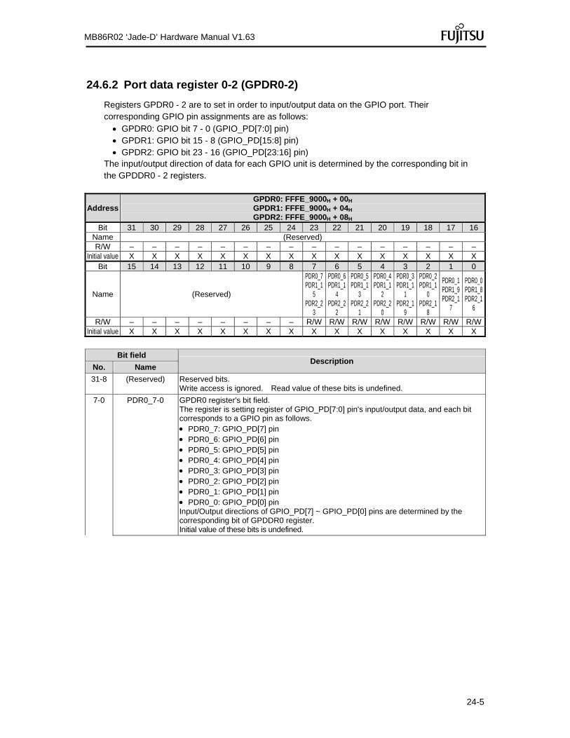
24-5
MB86R02 ‘Jade-D’ Hardware Manual V1.63
24.6.2 Port data register 0-2 (GPDR0-2)
Registers GPDR0 - 2 are to set in order to input/output data on the GPIO port. Their corresponding GPIO pin assignments are as follows: GPDR0: GPIO bit 7 - 0 (GPIO_PD[7:0] pin) GPDR1: GPIO bit 15 - 8 (GPIO_PD[15:8] pin) GPDR2: GPIO bit 23 - 16 (GPIO_PD[23:16] pin)
The input/output direction of data for each GPIO unit is determined by the corresponding bit in the GPDDR0 - 2 registers.
Address GPDR0: FFFE_9000H + 00H
GPDR1: FFFE_9000H + 04H
GPDR2: FFFE_9000H + 08H Bit 31 30 29 28 27 26 25 24 23 22 21 20 19 18 17 16
Name (Reserved) R/W – – – – – – – – – – – – – – – –
Initial value X X X X X X X X X X X X X X X X Bit 15 14 13 12 11 10 9 8 7 6 5 4 3 2 1 0
Name (Reserved)
PDR0_7PDR1_1
5 PDR2_2
3
PDR0_6PDR1_1
4 PDR2_2
2
PDR0_5PDR1_1
3 PDR2_2
1
PDR0_4PDR1_1
2 PDR2_2
0
PDR0_3 PDR1_1
1 PDR2_1
9
PDR0_2 PDR1_1
0 PDR2_1
8
PDR0_1PDR1_9PDR2_1
7
PDR0_0PDR1_8PDR2_1
6
R/W – – – – – – – – R/W R/W R/W R/W R/W R/W R/W R/WInitial value X X X X X X X X X X X X X X X X
Bit field
Description No. Name
31-8 (Reserved) Reserved bits. Write access is ignored. Read value of these bits is undefined.
7-0 PDR0_7-0 GPDR0 register's bit field. The register is setting register of GPIO_PD[7:0] pin's input/output data, and each bit corresponds to a GPIO pin as follows. PDR0_7: GPIO_PD[7] pin PDR0_6: GPIO_PD[6] pin PDR0_5: GPIO_PD[5] pin PDR0_4: GPIO_PD[4] pin PDR0_3: GPIO_PD[3] pin PDR0_2: GPIO_PD[2] pin PDR0_1: GPIO_PD[1] pin PDR0_0: GPIO_PD[0] pin Input/Output directions of GPIO_PD[7] ~ GPIO_PD[0] pins are determined by the corresponding bit of GPDDR0 register. Initial value of these bits is undefined.

24-6
MB86R02 ‘Jade-D’ Hardware Manual V1.63
Bit field Description
No. Name
PDR1_15-8 GPDR1 register's bit field. This register is setting register of GPIO_PD[15:8] pin's input/output data, and each bit corresponds to a GPIO pin as follows. PDR1_15: GPIO_PD[15] pin PDR1_14: GPIO_PD[14] pin PDR1_13: GPIO_PD[13] pin PDR1_12: GPIO_PD[12] pin PDR1_11: GPIO_PD[11] pin PDR1_10: GPIO_PD[10] pin PDR1_09: GPIO_PD[9] pin PDR1_08: GPIO_PD[8] pin Input/Output directions of GPIO_PD[15] ~ GPIO_PD[8] pins are determined by the corresponding bit of GPDDR1 register. Initial value of these bits is undefined.
7-0 PDR2_23-16 GPDR2 register's bit field. This register is setting register of GPIO_PD[23:16] pin's input/output data, and each bit corresponds to GPIO pin as follows. PDR2_23: GPIO_PD[23] pin PDR2_22: GPIO_PD[22] pin PDR2_21: GPIO_PD[21] pin PDR2_20: GPIO_PD[20] pin PDR2_19: GPIO_PD[19] pin PDR2_18: GPIO_PD[18] pin PDR2_17: GPIO_PD[17] pin PDR2_16: GPIO_PD[16] pin Input/Output directions of GPIO_PD[23] ~ GPIO_PD[16] pins are determined by the corresponding bit of GPDDR2 register. Initial value of these bits is undefined.

24-7
MB86R02 ‘Jade-D’ Hardware Manual V1.63
24.6.3 Data direction register 0-2 (GPDDR0-2)
GPDDR0 - 2 registers are to control input/output directions of GPIO port, and their corresponding GPIO pin is as follows. GPDDR0: GPIO bit 7 - 0 (GPIO_PD[7:0] pin) GPDDR1: GPIO bit 15 - 8 (GPIO_PD[15:8] pin) GPDDR2: GPIO bit 23 - 16 (GPIO_PD[23:16] pin)
Address GPDDR0: FFFE_9000H + 10H
GPDDR1: FFFE_9000H + 14H
GPDDR2: FFFE_9000H + 18H Bit 31 30 29 28 27 26 25 24 23 22 21 20 19 18 17 16
Name (Reserved) R/W – – – – – – – – – – – – – – – –
Initial value X X X X X X X X X X X X X X X X Bit 15 14 13 12 11 10 9 8 7 6 5 4 3 2 1 0
Name (Reserved)
DDR0_7DDR1_1
5 DDR2_2
3
DDR0_6DDR1_1
4 DDR2_2
2
DDR0_5DDR1_1
3 DDR2_2
1
DDR0_4DDR1_1
2 DDR2_2
0
DDR0_3 DDR1_1
1 DDR2_1
9
DDR0_2 DDR1_1
0 DDR2_1
8
DDR0_1DDR1_9DDR2_1
7
DDR0_0DDR1_8DDR2_1
6
R/W – – – – – – – – R/W R/W R/W R/W R/W R/W R/W R/WInitial value X X X X X X X X 0 0 0 0 0 0 0 0
Bit field
Description No. Name
31-8 (Reserved) Reserved bits. Write access is ignored. Read value of these bits is undefined.
7-0 DDR0_7-0 GPDR0 register's bit field. This register controls input/output directions of GPIO_PD[7:0] pin.
0 GPIO acts as an input port
1 GPIO acts as an output port GPIO pin corresponding to this register is as follows: DDR0_7: GPIO_PD[7] pin DDR0_6: GPIO_PD[6] pin DDR0_5: GPIO_PD[5] pin DDR0_4: GPIO_PD[4] pin DDR0_3: GPIO_PD[3] pin DDR0_2: GPIO_PD[2] pin DDR0_1: GPIO_PD[1] pin DDR0_0: GPIO_PD[0] pin These bits are initialized to "0" by reset.

24-8
MB86R02 ‘Jade-D’ Hardware Manual V1.63
Bit field Description
No. Name
7-0 DDR1_15-8 GPDDR1 register's bit field. This register controls input/output directions of GPIO_PD[15:8] pin.
0 GPIO acts as an input port
1 GPIO acts as an output port GPIO pin corresponding to this register is as follows: DDR1_15: GPIO_PD[15] pin DDR1_14: GPIO_PD[14] pin DDR1_13: GPIO_PD[13] pin DDR1_12: GPIO_PD[12] pin DDR1_11: GPIO_PD[11] pin DDR1_10: GPIO_PD[10] pin DDR1_9: GPIO_PD[9] pin DDR1_8: GPIO_PD[8] pin These bits are initialized to "1" by reset.
GPDDR2 register's bit field. This register controls input/output directions of GPIO_PD[23:16] pin
0 GPIO acts as an input port
1 GPIO acts as an output port GPIO pin corresponding to this register is as follows: DDR2_23: GPIO_PD[23] pin DDR2_22: GPIO_PD[22] pin DDR2_21: GPIO_PD[21] pin DDR2_20: GPIO_PD[20] pin DDR2_19: GPIO_PD[19] pin DDR2_18: GPIO_PD[18] pin DDR2_17: GPIO_PD[17] pin DDR2_16: GPIO_PD[16] pin These bits are initialized to "1" by reset.

24-9
MB86R02 ‘Jade-D’ Hardware Manual V1.63
24.7 Operation
This section describes the operation of the GPIO module.
24.7.1 Direction control
The direction of the GPIO ports (bits 23 – 0) can be changed using the GPDDRx register. The initial direction (the DDRx bit's initial value in the GPDDRx register) after reset is "0" (output port).
Note: Be careful to avoid a bus conflict when changing a GPIO port's direction.
24.7.2 Data transfer
When a GPIO port is used as an input port (DDRx = 0), the data signal input to the port input signal (PI) is stored in PDRx (in) on the rising edge of the APB clock (see Figure 13-1). Input data can be read via the GPDRx register. During the period, write access to the GPDRx register is valid and PDRx (out) is changeable except when DDRx = 0. When the GPIO port is used as an output port (DDR = 1), the GPDRx register value is output to the port output signal (PO); during which the read data of the register assumes the same value as the port output signal's value.

25-1
MB86R02 ‘Jade-D’ Hardware Manual V1.63
25 Pulse Width Modulator (PWM) This chapter describes operation and function of the PWM (Pulse Width Modulator) units.
25.1 Outline
MB86R02 has 8 PWM channels which are able to output high-precision PWM wave patterns efficiently.
25.2 Feature
The PWM unit has the following features: 8 embedded channels Individual settings possible for duty ratio, phase and polarity Configurable one-shot output/continuous output of the pulse

25-2
MB86R02 ‘Jade-D’ Hardware Manual V1.63
25.3 Block diagram
Figure 14-1 shows a block diagram of the PWM unit.
CLKgenerator
AP
B b
us
PULSE
generator
PWM module
AP
B I
/F
IRC
PWM_O0
PWM_O1
PWM_O2
.
.
PWM_O7
Int0..7 8
Figure 25-1 PWM block diagram
25.4 Related pins
The availability of PWM pins depends on the follow CCNT (JCNT) registers: • Set to CMPX_MODE_6 = "1B" of multiplex mode setting register to make PWM[7:4] available • Set to CMPX_MODE_7 = "0B" of multiplex mode setting register to make PWM[3:0] available
25.5 Clock Supply
The APB clock is supplied to the PWM unit. Please refer to the chapter 'Clock Reset Generator (CRG)' for details on setting the frequency and controlling the clock.
25.6 Interrupts
When an interrupt vector occurs, the PWM notifies the IRC. Please refer to the 'Interrupt Controller (IRC)' chapter for more details.
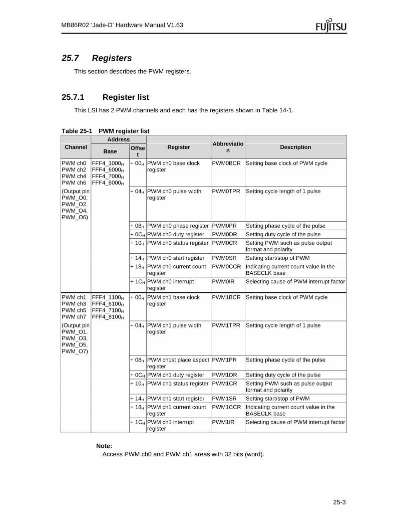
25-3
MB86R02 ‘Jade-D’ Hardware Manual V1.63
25.7 Registers
This section describes the PWM registers.
25.7.1 Register list
This LSI has 2 PWM channels and each has the registers shown in Table 14-1.
Table 25-1 PWM register list
Channel Address
Register Abbreviatio
n Description
Base Offse
t
PWM ch0 PWM ch2 PWM ch4 PWM ch6
FFF4_1000H
FFF4_6000H
FFF4_7000H
FFF4_8000H
+ 00H PWM ch0 base clock register
PWM0BCR Setting base clock of PWM cycle
(Output pin PWM_O0, PWM_O2, PWM_O4, PWM_O6)
+ 04H PWM ch0 pulse width register
PWM0TPR Setting cycle length of 1 pulse
+ 08H PWM ch0 phase register PWM0PR Setting phase cycle of the pulse
+ 0CH PWM ch0 duty register PWM0DR Setting duty cycle of the pulse
+ 10H PWM ch0 status register PWM0CR Setting PWM such as pulse output format and polarity
+ 14H PWM ch0 start register PWM0SR Setting start/stop of PWM
+ 18H PWM ch0 current count register
PWM0CCR Indicating current count value in the BASECLK base
+ 1CH PWM ch0 interrupt register
PWM0IR Selecting cause of PWM interrupt factor
PWM ch1 PWM ch3 PWM ch5 PWM ch7
FFF4_1100H
FFF4_6100H FFF4_7100H FFF4_8100H
+ 00H PWM ch1 base clock register
PWM1BCR Setting base clock of PWM cycle
(Output pin PWM_O1, PWM_O3, PWM_O5, PWM_O7)
+ 04H PWM ch1 pulse width register
PWM1TPR Setting cycle length of 1 pulse
+ 08H PWM ch1st place aspect register
PWM1PR Setting phase cycle of the pulse
+ 0CH PWM ch1 duty register PWM1DR Setting duty cycle of the pulse
+ 10H PWM ch1 status register PWM1CR Setting PWM such as pulse output format and polarity
+ 14H PWM ch1 start register PWM1SR Setting start/stop of PWM
+ 18H PWM ch1 current count register
PWM1CCR Indicating current count value in the BASECLK base
+ 1CH PWM ch1 interrupt register
PWM1IR Selecting cause of PWM interrupt factor
Note:
Access PWM ch0 and PWM ch1 areas with 32 bits (word).

25-4
MB86R02 ‘Jade-D’ Hardware Manual V1.63
Format of register description Following format is used for description of register’s each bit in "14.7.2 PWMx base clock register (PWMxBCR)" to "14.7.9 PWMx interrupt register (PWMxIR)".
Address Base address + Offset Bit 31 30 29 28 27 26 25 24 23 22 21 20 19 18 17 16
Name R/W
Initial value Bit 15 14 13 12 11 10 9 8 7 6 5 4 3 2 1 0
Name R/W
Initial value
Meaning of item and sign Address
Address (base address + offset address) of the register Bit
Bit number of the register Name
Bit field name of the register R/W
Attribution of read/write of each bit field R0:Read value is always "0" R1: Read value is always "1" W0: Write value is always "0", and write access of "1" is ignored W1: Write value is always "1", and write access of "0" is ignored R: Read W: Write Initial value
Each bit field’s value after reset 0: Value is "0" 1: Value is "1" X: Value is undefined

25-5
MB86R02 ‘Jade-D’ Hardware Manual V1.63
25.7.2 PWMx base clock register (PWMxBCR)
This register is to set base clock of PWM cycle.
Address
ch0:FFF4_1000 + 00H ch1:FFF4_1100 + 00H
ch2:FFF4_6000 + 00H ch3:FFF4_6100 + 00H
ch4:FFF4_7000 + 00H ch5:FFF4_7100 + 00H
ch6:FFF4_8000 + 00H ch7:FFF4_8100 + 00H
Bit 31 30 29 28 27 26 25 24 23 22 21 20 19 18 17 16 Name (Reserved) R/W R R R R R R R R R R R R R R R R
Initial value 0 0 0 0 0 0 0 0 0 0 0 0 0 0 0 0 Bit 15 14 13 12 11 10 9 8 7 6 5 4 3 2 1 0
Name BCR[15:0] R/W R/W R/W R/W R/W R/W R/W R/W R/W R/W R/W R/W R/W R/W R/W R/W R/W
Initial value 0 0 0 0 0 0 0 0 0 0 0 0 0 0 0 0
Bit field
Description No. Name
31-16 (Reserved) Reserved bits. Write access is ignored. The read value of these bits is always "0".
15-0 BCR Sets the base clock of the PWM cycle.
BCR[15:0] Base clock
0 0 APBCLK (Setting
prohibited)
1 1 APBCLK
| |
65535 65535 APBCLK

25-6
MB86R02 ‘Jade-D’ Hardware Manual V1.63
25.7.3 PWMx pulse width register (PWMxTPR)
This register is to set cycle length of 1 pulse.
Address
ch0:FFF4_1000 + 04H ch1:FFF4_1100 + 04H
ch2:FFF4_6000 + 04H ch3:FFF4_6100 + 04H
ch4:FFF4_7000 + 04H ch5:FFF4_7100 + 04H
ch6:FFF4_8000 + 04H ch7:FFF4_8100 + 04H
Bit 31 30 29 28 27 26 25 24 23 22 21 20 19 18 17 16 Name (Reserved) R/W R R R R R R R R R R R R R R R R
Initial value 0 0 0 0 0 0 0 0 0 0 0 0 0 0 0 0 Bit 15 14 13 12 11 10 9 8 7 6 5 4 3 2 1 0
Name TPR[15:0] R/W R/W R/W R/W R/W R/W R/W R/W R/W R/W R/W R/W R/W R/W R/W R/W R/W
Initial value 0 0 0 0 0 0 0 0 0 0 0 0 0 0 0 0
Bit field
Description No. Name
31-16 (Reserved) Reserved bits. Write access is ignored. The read value of these bits is always "0".
15-0 TPR Cycle length of 1 pulse shown in Figure 14-2 is set.
TPR[15:0] Pulse cycle length
0 0 BASECLK (Setting prohibited)
1 1 BASECLK (Setting prohibited)
2 2 BASECLK
| |
65535 65535 BASECLK
APBCLK
BASECLK
PWM
Phase
Duty
Next cycle (skippable)
Pulse width (1 cycle)
Figure 25-2 Setting parameter

25-7
MB86R02 ‘Jade-D’ Hardware Manual V1.63
25.7.4 PWMx phase register (PWMxPR)
This register is to set phase cycle of the pulse.
Address
ch0:FFF4_1000 + 08H ch1:FFF4_1100 + 08H
ch2:FFF4_6000 + 08H ch3:FFF4_6100 + 08H
ch4:FFF4_7000 + 08H ch5:FFF4_7100 + 08H
ch6:FFF4_8000 + 08H ch7:FFF4_8100 + 08H
Bit 31 30 29 28 27 26 25 24 23 22 21 20 19 18 17 16 Name (Reserved) R/W R R R R R R R R R R R R R R R R
Initial value 0 0 0 0 0 0 0 0 0 0 0 0 0 0 0 0 Bit 15 14 13 12 11 10 9 8 7 6 5 4 3 2 1 0
Name PR[15:0] R/W R/W R/W R/W R/W R/W R/W R/W R/W R/W R/W R/W R/W R/W R/W R/W R/W
Initial value 0 0 0 0 0 0 0 0 0 0 0 0 0 0 0 0
Bit field
Description No. Name
31-16 (Reserved) Reserved bits. Write access is ignored. The read value of these bits is always "0".
15-0 PR Phase cycle shown in Figure 14-3 is set.
PR[15:0] Phase cycle
0 0 BASECLK (Setting
prohibited)
1 1 BASECLK
| |
65535 65535 BASECLK
APBCLK
BASECLK
PWM
Phase
Duty
Next cycle (skippable)
Pulse width (1 cycle)
Figure 25-3 Setting parameter

25-8
MB86R02 ‘Jade-D’ Hardware Manual V1.63
25.7.5 PWMx duty register (PWMxDR)
This register is to set duty cycle of the pulse.
Address
ch0:FFF4_1000 + 0CH ch1:FFF4_1100 + 0CH
ch2:FFF4_6000 + 0CH ch3:FFF4_6100 + 0CH
ch4:FFF4_7000 + 0CH ch5:FFF4_7100 + 0CH
ch6:FFF4_8000 + 0CH ch7:FFF4_8100 + 0CH
Bit 31 30 29 28 27 26 25 24 23 22 21 20 19 18 17 16 Name (Reserved) R/W R R R R R R R R R R R R R R R R
Initial value 0 0 0 0 0 0 0 0 0 0 0 0 0 0 0 0 Bit 15 14 13 12 11 10 9 8 7 6 5 4 3 2 1 0
Name DR[15:0] R/W R/W R/W R/W R/W R/W R/W R/W R/W R/W R/W R/W R/W R/W R/W R/W R/W
Initial value 0 0 0 0 0 0 0 0 0 0 0 0 0 0 0 0
Bit field
Description No. Name
31-16
(Reserved) Reserved bits. Write access is ignored. The read value of these bits is always "0".
15-0 DR Duty cycle shown in Figure 14-4 is set.
DR[15:0] Duty cycle
0 0 BASECLK (Setting prohibited)
1 1 BASECLK
| |
65535 65535 BASECLK
APBCLK
BASECLK
PWM
Phase
Duty
Next cycle (skippable)
Pulse width (1 cycle)
Figure 25-4 Setting parameter

25-9
MB86R02 ‘Jade-D’ Hardware Manual V1.63
25.7.6 PWMx status register (PWMxCR)
This register is to set PWM such as pulse output format and polarity.
Address
ch0:FFF4_1000 + 10H ch1:FFF4_1100 + 10H
ch2:FFF4_6000 + 10H ch3:FFF4_6100 + 10H
ch4:FFF4_7000 + 10H ch5:FFF4_7100 + 10H
ch6:FFF4_8000 + 10H ch7:FFF4_8100 + 10H
Bit 31 30 29 28 27 26 25 24 23 22 21 20 19 18 17 16 Name (Reserved) R/W R R R R R R R R R R R R R R R R
Initial value 0 0 0 0 0 0 0 0 0 0 0 0 0 0 0 0 Bit 15 14 13 12 11 10 9 8 7 6 5 4 3 2 1 0
Name (Reserved) ONESHOT (Reserved) POL R/W R R R R R R R R R R R R R/W R/W R/W R/W
Initial value 0 0 0 0 0 0 0 0 0 0 0 0 0 0 0 0
Bit field
Description No. Name
31-4 (Reserved) Reserved bits. Write access is ignored. The read value of these bits is always "0".
3 ONESHOT Pulse output format, either continuous output or one-shot output is set.
0 Continuous output (initial value)
1 One-shot output
2-1 (Reserved) Reserved bits. Write "0" to these bits. Read value of these bits are undefined. Note: Writing "1" to these bits is prohibited.
0 POL Polarity of the pulse is set.
0 Negative pulse (initial value)
1 Positive pulse

25-10
MB86R02 ‘Jade-D’ Hardware Manual V1.63
25.7.7 PWMx start register (PWMxSR)
This register is to set PWM start-up/stop.
Address
ch0:FFF4_1000 + 14H ch1:FFF4_1100 + 14H
ch2:FFF4_6000 + 14H ch3:FFF4_6100 + 14H
ch4:FFF4_7000 + 14H ch5:FFF4_7100 + 14H
ch6:FFF4_8000 + 14H ch7:FFF4_8100 + 14H
Bit 31 30 29 28 27 26 25 24 23 22 21 20 19 18 17 16 Name (Reserved) R/W R R R R R R R R R R R R R R R R
Initial value 0 0 0 0 0 0 0 0 0 0 0 0 0 0 0 0 Bit 15 14 13 12 11 10 9 8 7 6 5 4 3 2 1 0
Name (Reserved) STARTR/W R R R R R R R R R R R R R R R R/W
Initial value 0 0 0 0 0 0 0 0 0 0 0 0 0 0 0 0
Bit field
Description No. Name
31-1 (Reserved) Reserved bits. Write access is ignored. The read value of these bits is always "0".
0 START Start-up/Stop of PWM are set.
0 Stop (initial value)
1 Start-up After pulse cycle ends, this bit is cleared to "0" when ONSHOT bit = 1 of PWMxCR register.

25-11
MB86R02 ‘Jade-D’ Hardware Manual V1.63
25.7.8 PWMx current count register (PWMxCCR)
This register is to indicate current count value in BASECLK base.
Address
ch0:FFF4_1000 + 18H ch1:FFF4_1100 + 18H
ch2:FFF4_6000 + 18H ch3:FFF4_6100 + 18H
ch4:FFF4_7000 + 18H ch5:FFF4_7100 + 18H
ch6:FFF4_8000 + 18H ch7:FFF4_8100 + 18H
Bit 31 30 29 28 27 26 25 24 23 22 21 20 19 18 17 16 Name (Reserved) R/W R R R R R R R R R R R R R R R R
Initial value 0 0 0 0 0 0 0 0 0 0 0 0 0 0 0 0 Bit 15 14 13 12 11 10 9 8 7 6 5 4 3 2 1 0
Name CCR[15:0] R/W R R R R R R R R R R R R R R R R
Initial value X X X X X X X X X X X X X X X X
Bit field
Description No. Name
31-16 (Reserved) Reserved bits. Write access is ignored. The read value of these bits is always "0".
15-0 CCR Current count value in BASECLK base is indicated.
CCR[15:0] Duty cycle
0 0 BASECLK
1 1 BASECLK
| |
65535 65535 BASECLK

25-12
MB86R02 ‘Jade-D’ Hardware Manual V1.63
25.7.9 PWMx interrupt register (PWMxIR)
This register is to select cause of PWM interrupt.
Address
ch0:FFF4_1000 + 1CH ch1:FFF4_1100 + 1CH
ch2:FFF4_6000 + 1CH ch3:FFF4_6100 + 1CH
ch4:FFF4_7000 + 1CH ch5:FFF4_7100 + 1CH
ch6:FFF4_8000 + 1CH ch7:FFF4_8100 + 1CH
Bit 31 30 29 28 27 26 25 24 23 22 21 20 19 18 17 16 Name (Reserved) R/W R R R R R R R R R R R R R R R R
Initial value 0 0 0 0 0 0 0 0 0 0 0 0 0 0 0 0 Bit 15 14 13 12 11 10 9 8 7 6 5 4 3 2 1 0
Name (Reserved) INTREP[1:0
] (Reserved) DONE
R/W R R R R R R R/W R/W R R R R R R R/W1 R/W1Initial value 0 0 0 0 0 0 0 0 0 0 0 0 0 0 0 0
Bit field
Description No. Name
31-10 (Reserved) Reserved bits. Write access is ignored. The read value of these bits is always "0".
9-8 INTREP[1:0] The bit (DONE bit) which might be the cause of PWM interrupt is selected. INTREP[1:0] Possible cause bit for PWM interrupt
00 DONE bit is not selected
01 DONE bit is selected as cause of interrupt factor
10 (Setting prohibited)
11 (Setting prohibited)
7-1 (Reserved) Reserved bits. Write access is ignored. The read value of these bits is always "0".
0 DONE This bit indicates end of 1 pulse cycle.
0 1 pulse is not output (initial value)
1 1 pulse is output This bit is cleared to "0" by writing "1".

25-13
MB86R02 ‘Jade-D’ Hardware Manual V1.63
25.8 Example of setting a register
This section provides an example of a register's initial setting.
Power-on
Set PWMx base clock register (PWMxBCR)
Set polarity (POL) and one-shot (ONESHOT) pulses
Set PWMx pulse width register (PWMxTPR)
Set PWMx phase register (PWMxPR)
Set PWMx duty register (PWMxDR)
Set PWMx status register (PWMxCR)
Set PWMx activation register (PWMxSR) PWM is activated
PWMx interrupt register's INTREP bit = 01B
Output 1 pulse cycle
Yes
Interrupt occurs
No
PWMxSR start bit = 1 Yes
No
End
PWM stops with negating start bit (PWMxSR START bit) at completing pulse cycle, not immediately after negating the start bit
Set each register in the following condition: PWMx base clock register 1 PWMx phase register 1 PWMx duty register 1 PWMx phase register + PWMx duty register PWMx pulse width register 2
(The next phase setting after duty operation is omitted)

26-1
MB86R02 ‘Jade-D’ Hardware Manual V1.63
26 A/D Converter This chapter describes the functionality and operation of the A/D converters.
26.1 Outline
MB86R02 'JADE-D' has 4 A/D converter channels.
26.2 Features
Successive approximation A/D converter Max. conversion rate: Approx. 648K samples/sec, 10 bit resolution Immediate reading operation of A/D value by analog data auto. polling operation A/D converter operation clock dividing ratio can be selected: 1/4 (APB clock is 41.5MHz: Approx. 648.4K samples/sec) 1/8 (APB clock is 41.5MHz: Approx. 324.1K samples/sec) 1/16 (APB clock is 41.5MHz: Approx. 162.0K samples/sec) 1/32 (APB clock is 41.5MHz: Approx. 81.0K samples/sec) 1/64 (APB clock is 41.5MHz: Approx. 40.5K samples/sec) 1/256 (APB clock is 41.5MHz: Approx. 10.1K samples/sec) 1/1024 (APB clock is 41.5MHz: Approx. 2.5K samples/sec) 1/4096 (APB clock is 41.5MHz: Approx. 0.6K samples/sec)

26-2
MB86R02 ‘Jade-D’ Hardware Manual V1.63
26.3 Block diagram
Figure 15-1 shows a block diagram of the A/D converter.
APB IF APB IF
AD_VR0/AD_VR1
A/D Converter
10bit DAC
10bit Register
SAR
Sample & Hold
External
AD_VRH0/AD_VRH1
AD_VRL0/AD_VRL1
ComparatorAD_VIN0/AD_VIN1
Figure 26-1 Block diagram of A/D converter
26.4 Related pins
A/D converter uses following pins. Pin Direction Qty. Description
AD_VIN0 IN 1 A/D analog input pin
AD_VIN1 IN 1 A/D analog input pin
AD_VIN2 IN 1 A/D analog input pin
AD_VIN3 IN 1 A/D analog input pin
AD_VRH0 IN 1 Reference voltage "H" input pin
AD_VRH1 IN 1 Reference voltage "H" input pin
AD_VRL0 IN 1 Reference voltage "L" input pin
AD_VRL1 IN 1 Reference voltage "L" input pin
AD_VR0 OUT 1 Reference output
AD_VR1 OUT 1 Reference output
AD_AVD0 IN 1 Analog power supply pin
AD_AVS1 IN 1 Analog GND
26.5 Supply clock
The APB clock is supplied to the A/D converter. Refer to "5. Clock reset generator (CRG)" for frequency setting and control specification of the clock.

26-3
MB86R02 ‘Jade-D’ Hardware Manual V1.63
26.6 Channel mapping table
This table shows the channel mapping to the ADC units analog inputs:
ADC instance Input number of instance Channel number Pin
0 0 0 AD_VIN0 1 2 AD_VIN2
1 0 1 AD_VIN1 1 3 AD_VIN3
26.7 Output truth value list
Example of truth value of A/D converter is shown below.
Ideal input level Output code VIN[V] D9 D8 D7 D6 D5 D4 D3 D2 D1 D0
2.2485 ... H H H H H H H H H H 2.2471 ... 2.2485
H H H H H H H H H L
2.2456 ... 2.2471
H H H H H H H H L H
0.7515 ... 0.7529
L L L L L L L L L H
... 0.7515 L L L L L L L L L L Note: AD_AVD0 = 3.0V, AD_VRH0/AD_VRH1 = 2.25V, AD_ VRL0/AD_VRL1 = 0.75V
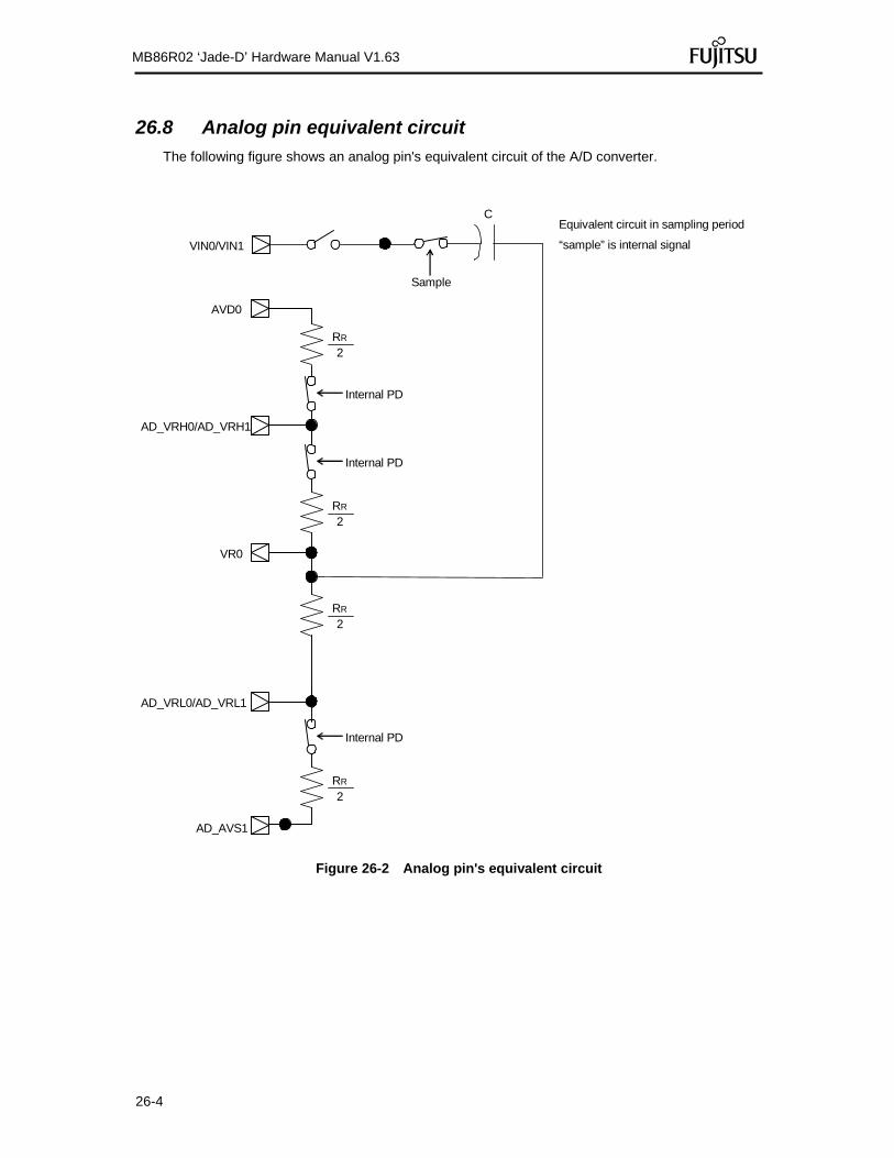
26-4
MB86R02 ‘Jade-D’ Hardware Manual V1.63
26.8 Analog pin equivalent circuit
The following figure shows an analog pin's equivalent circuit of the A/D converter.
Sample
C Equivalent circuit in sampling period
“sample” is internal signal
VR0
Internal PD
2 RR
2 RR
Internal PD
2 RR
AVD0
AD_AVS1
2 RR
Internal PD
AD_VRH0/AD_VRH1
AD_VRL0/AD_VRL1
VIN0/VIN1
Figure 26-2 Analog pin's equivalent circuit

26-5
MB86R02 ‘Jade-D’ Hardware Manual V1.63
26.9 Registers
This section describes the A/D converter registers.
26.9.1 Register list
This LSI has 2 ADC instances controlling 4 channels. The registers shown below in Table 15-1 control the ADC functionality of the device.
Table 26-1 Register Summary
Channel Address
Register Abbreviation Description Base Offset
ADC 0 FFF5_2000H + 00H ADC 0 data register ADC0DATA A/D converted data is stored
+ 04H ADC0 mode register ADC0MODE Sampling mode is set
+ 08H ADC 0 power down control register
ADC0XPD Power down mode is set/released
+ 0CH (Reserved) – Reserved area, access prohibited
+ 10H ADC 0 clock selection register
ADC0CKSEL Clock frequency is supplied to A/D converter
+ 14H ADC 0 status register ADC0STATUS A/D converted data is stored to data register
ADC 1 FFF5_3000H + 00H ADC 1 data register ADC1DATA A/D converted data is stored
+ 04H ADC1 mode register ADC1MODE Sampling mode is set
+ 08H Down of ADC 1 power control register
ADC1XPD Power down mode is set/released
+ 0CH (Reserved) – Reserved area, access prohibited
+ 10H ADC 1 clock selection register
ADC1CKSEL Clock frequency is supplied to A/D converter
+ 14H ADC 1 status register ADC1STATUS A/D converted data is stored to data register
Note: Access all ADC channel areas using 32 bit (word) accesses.

26-6
MB86R02 ‘Jade-D’ Hardware Manual V1.63
26.9.2 Format of Register Descriptions
The register descriptions in the following sections use the format shown below to describe each bit field of a register. Register address Offset
Bit number 31 30 29 28 27 26 25 24 23 22 21 20 19 18 17 16 15 14 13 12 11 10 9 8 7 6 5 4 3 2 1 0
Field name
R/W
Reset value
Meaning of items and sign Register address
Register address shows the address (Offset address) of the register. Bit number
Bit number shows bit position of the register. Field name
Field name shows bit name of the register. R/W
R/W shows the read/write attribute of each bit field: R: Read W: Write W1C: Writing a value of "1" clears the register.
Reset value Reset value indicates the value of each bit field immediately after reset. 0: Initial value is "0". 1: Initial value is "1". X: Undefined.
Unused register fields are marked with a solid grey background. Bit vectors are unsigned integers, if nothing else specified. Please note, that access to an address with no register results in an error response.

26-7
MB86R02 ‘Jade-D’ Hardware Manual V1.63
26.9.3 ADCx data register (ADCxDATA)
This register is to store A/D converted data.
Address instance 0:FFF5_2000 + 00H instance 1:FFF5_3000 + 00H
Bit 31 30 29 28 27 26 25 24 23 22 21 20 19 18 17 16 Name (Reserved) DATA1[9:0] R/W R0 R0 R0 R0 R0 R0 R R R R R R R R R R
Initial value 0 0 0 0 0 0 0 0 0 0 0 0 0 0 0 0 Bit 15 14 13 12 11 10 9 8 7 6 5 4 3 2 1 0
Name (Reserved) DATA0[9:0] R/W R0 R0 R0 R0 R0 R0 R R R R R R R R R R
Initial value 0 0 0 0 0 0 0 0 0 0 0 0 0 0 0 0
Bit field
Description No. Name
31-26 (Reserved) It is a reserved bit. Write access is ignored. Read value of these bits is always “0”.
25-16 DATA1[9:0] Output data from A/D converter input 1 is stored with polling operation. When power down mode is set to release at ADCx power down control register (ADCxXPD), data is imported to this register.
15-10 (Reserved) It is a reserved bit. Write access is ignored. Read value of these bits is always “0”.
9-0 DATA0[9:0] Output data from A/D converter input 0 is stored with polling operation. When power down mode is set to release at ADCx power down control register (ADCxXPD), data is imported to this register.
26.9.4 ADCx mode register (ADCxMODE)
This register is to set the sampling mode.
Address instance 0:FFF5_2000 + 04H instance 1:FFF5_3000 + 04H
Bit 31 30 29 28 27 26 25 24 23 22 21 20 19 18 17 16 Name (Reserved) R/W R0 R0 R0 R0 R0 R0 R0 R0 R0 R0 R0 R0 R0 R0 R0 R0
Initial value 0 0 0 0 0 0 0 0 0 0 0 0 0 0 0 0 Bit 15 14 13 12 11 10 9 8 7 6 5 4 3 2 1 0
Name (Reserved) MODE[1:0]R/W R0 R0 R0 R0 R0 R0 R0 R0 R0 R0 R0 R0 R0 R0 R/W R/W
Initial value 0 0 0 0 0 0 0 0 0 0 0 0 0 0 0 0
Bit field
Description No. Name
31-2 (Reserved) It is a reserved bit. Write access is ignored. Read value of these bits is always “0”.
1-0 MODE[1:0] Sample Mode. If it is 2’b00, only input 0 is continuously sampled, if it is 2’b01, only input 1 is continuously sampled, if it is 2’b10, both inputs are continuously sampled interleaved, setting 2’b11 is reserved
26.9.5 ADCx power down control register (ADCxXPD)
This register is to control A/D converter operation.

26-8
MB86R02 ‘Jade-D’ Hardware Manual V1.63
Address instance 0:FFF5_2000 + 08H instance 1:FFF5_3000 + 08H
Bit 31 30 29 28 27 26 25 24 23 22 21 20 19 18 17 16 Name (Reserved) R/W R0 R0 R0 R0 R0 R0 R0 R0 R0 R0 R0 R0 R0 R0 R0 R0
Initial value 0 0 0 0 0 0 0 0 0 0 0 0 0 0 0 0 Bit 15 14 13 12 11 10 9 8 7 6 5 4 3 2 1 0
Name (Reserved) XPDR/W R0 R0 R0 R0 R0 R0 R0 R0 R0 R0 R0 R0 R0 R0 R0 R/W
Initial value 0 0 0 0 0 0 0 0 0 0 0 0 0 0 0 0
Bit field
Description No. Name
31-1 (Reserved) It is a reserved bit. Write access is ignored. Read value of these bits is always "0".
0 XPD A/D converter operation is controlled.
0 Power down mode (initial value)
1 Release of power down mode When "1" is written to XPD bit, A/D converter's power-down mode is released and A/D data polling starts. Writing "0" to the bit sets A/D converter's power-down mode and A/D data polling stops.
26.9.6 ADCx clock selection register (ADCxCKSEL)
This register is to se to specify ADC clock frequency supplying to A/D converter. This setting enables sampling plate change.
Address instance 0:FFF5_2000 + 10H instance 1:FFF5_3000 + 10H
Bit 31 30 29 28 27 26 25 24 23 22 21 20 19 18 17 16 Name (Reserved) R/W R0 R0 R0 R0 R0 R0 R0 R0 R0 R0 R0 R0 R0 R0 R0 R0
Initial value 0 0 0 0 0 0 0 0 0 0 0 0 0 0 0 0 Bit 15 14 13 12 11 10 9 8 7 6 5 4 3 2 1 0
Name (Reserved) CKSEL[2:0] R/W R0 R0 R0 R0 R0 R0 R0 R0 R0 R0 R0 R0 R0 R/W R/W R/W
Initial value 0 0 0 0 0 0 0 0 0 0 0 0 0 0 0 0
Bit field
Description No. Name
31-3 (Reserved) It is a reserved bit. Write access is ignored. Read value of these bits is always "0".

26-9
MB86R02 ‘Jade-D’ Hardware Manual V1.63
Bit field Description
No. Name
2-0 CKSEL[2:0] Specify clock frequency supplying to A/D converter.
CKSEL[2:0] Clock frequency setting Sampling late [samples/sec.]
000B 1/4096 0.6K
001B 1/1024 2.5K
010B 1/256 10.1K
011B 1/64 40.5K
100B 1/32 81.0K
101B 1/16 162.0K
110B 1/8 324.1K
111B 1/4 648.4K This clock is made dividing APB clock (41.5MHz.) Analog voltage sampling is carried out every 16 cycles of clock set in this register.

26-10
MB86R02 ‘Jade-D’ Hardware Manual V1.63
26.9.7 ADCx status register (ADCxSTATUS)
This register is to indicate whether A/D data conversion is completed.
Address instance 0:FFF5_2000 + 14H instance 1:FFF5_3000 + 14H
Bit 31 30 29 28 27 26 25 24 23 22 21 20 19 18 17 16 Name (Reserved) R/W R0 R0 R0 R0 R0 R0 R0 R0 R0 R0 R0 R0 R0 R0 R0 R0
Initial value 0 0 0 0 0 0 0 0 0 0 0 0 0 0 0 0 Bit 15 14 13 12 11 10 9 8 7 6 5 4 3 2 1 0
Name (Reserved) CMP1 CMP
0 R/W R0 R0 R0 R0 R0 R0 R0 R0 R0 R0 R0 R0 R0 R0 R/W0 R/W0
Initial value 0 0 0 0 0 0 0 0 0 0 0 0 0 0 0 0
Bit field
Description No. Name
31-2 (Reserved) It is a reserved bit. Write access is ignored. Read value of these bits is always "0".
1 CMP1 Whether A/D data conversion is completed for input 1 is indicated.
0 A/D data conversion is not completed (initial value)
1 A/D data conversion is completed At the time data is set to ADCxDATA, CMP bit becomes "1". Writing "0" to the bit clears register value (although "1" is written to CMP bit, register bit value does not change.) Setting "1" to CMP bit outputs interrupt.
0 CMP0 Whether A/D data conversion is completed for input 0 is indicated.
0 A/D data conversion is not completed (initial value)
1 A/D data conversion is completed At the time data is set to ADCxDATA, CMP bit becomes "1". Writing "0" to the bit clears register value (although "1" is written to CMP bit, register bit value does not change.) Setting "1" to CMP bit outputs interrupt.

26-11
MB86R02 ‘Jade-D’ Hardware Manual V1.63
26.10 Basic operation flow
Basic operation flow of ADC is shown below.
Set of ADCxCKSEL Write "0x0 - 0x7" to ADCxCKSEL register
Power-on
After 16 ADC clocks, analog data is converted into digital data.In ADCxMODE = 2'b10 the wo inputs are sampled interleaved.
Set of ADCxXPDWrite "0x1" to ADCxXPD register(The polling of data starts)
* The data value is updatedonly every 16 ADC clocks though ADCxDATA registercan be read at any time.
In mode = 2'b10 every data result is only sampled every 32 ADC clock cycles.
Set converted A/D data to ADCxDATA register. (A range of data is "0x0 - 0x3FF")
The value of ADCxSTATUS register doesn't change if ADCxSTATUS register is "0x1".
If ADCxSTATUS register is "0x0", the value of ADCxSTATUS register becomes "0x1".
In ADCxMODE = 2'b10 the two inputs are sampled interleaved.
INT clear?
INT
NO
YES
Set of ADCxSTATUSWrite "0x0" to ADCxSTATUS register
Set of ADCxMODE Write "0x0 - 0x2" to ADCxMODE register

27-1
MB86R02 ‘Jade-D’ Hardware Manual V1.63
27 Serial Audio Interface (I2S) This chapter describes function and operation of serial audio interface (hereafter called, I2S.)
27.1 Outline
MB86R02 incorporates a one channel audio I/O interface in I2S format. Note: I2S stands for the Inter-IC Sound Bus by Philips Semiconductors (now NXP).
27.2 Features
I2S interface in MB86R02 has following features: Selecting master/slave operations by programmable Supporting state of transmission only, reception only, and simultaneous
transmission/reception Selecting 1 sub frame and 2 sub frame constructions Setting up to 32 channels to each sub frame Individually setting number of channel in each sub frame Individually setting channel length of each sub frame (number channel bit) Individually setting word length in channel of each sub frame Setting valid/invalid of each channel in each sub frame (Note 1) Setting word length from 7 to 32 bit Programming frequency of frame synchronous signal Setting up to 3071 bit in 1 frame Programming width of frame synchronous signal (1 bit or 1 channel length) Programming phase of frame synchronous signal (0 bits or 1 bit delay) Setting polarity of frame synchronous signal Setting polarity of serial bit clock Programming sampling point of received data Selecting clock frequency dividing source of serial bit clock in the master mode (internal and
external clock.) Setting clock frequency dividing ratio in the master mode
Frequency of I2S_SCLK = frequency of AHB clock (or external clock)/2 CKRT[5:0] Frequency dividing ratio is settable within 0 – 126 in multiple of 2 (when the ratio is 0, frequency dividing source is by-passed)
Data transfer to system memory by DMA (block transfer only, refer to the DMA chapter), interrupt, and polling
Note 1: Data is not sent or received to invalid channels

27-2
MB86R02 ‘Jade-D’ Hardware Manual V1.63
27.3 Block diagram
Figure 27-1 shows block diagram of I2S. As shown below, MB86R02 has 1 I2S channel.
Figure 27-1 Block diagram of I2S

27-3
MB86R02 ‘Jade-D’ Hardware Manual V1.63
27.4 Related pins
The availability of I2S IF pins depends on follow registers of CCNT (JCNT) : • Set to CMPX_MODE_6 = "0B" of multiplex mode setting register
27.5 Supply clock
AHB clock is supplied to I2S interface unit. Refer to "5. Clock reset generator (CRG)" for frequency setting and control specification of the clock.

27-4
MB86R02 ‘Jade-D’ Hardware Manual V1.63
27.6 Registers
This section describes I2S register.
27.6.1 Register list
Register relating to I2S control is shown below.
Module Address Register Function
I2S ch0 FFEE_0000 I2S0RXFDAT Reception FIFO data register
FFEE_0004 I2S0TXFDAT Transmission FIFO data register
FFEE_0008 I2S0CNTREG Control register
FFEE_000C I2S0MCR0REG Channel control register 0
FFEE_0010 I2S0MCR1REG Channel control register 1
FFEE_0014 I2S0MCR2REG Channel control register 2
FFEE_0018 I2S0OPRREG Operation control register
FFEE_001C I2S0SRST Software reset register
FFEE_0020 I2S0INTCNT Interrupt control register
FFEE_0024 I2S0STATUS STATUS register
FFEE_0028 I2S0DMAACT DMA start-up register
All registers of I2S correspond to access in byte (8 bit), half word (16 bit), and word (32 bit.)

27-5
MB86R02 ‘Jade-D’ Hardware Manual V1.63
27.6.2 Description format of registers
Following format is used for description of register’s each bit in "27.6.3 I2SxRXFDAT register" to "27.6.13 I2SxDMAACT register".
Address Base address + OffsetBit 31 30 29 28 27 26 25 24 23 22 21 20 19 18 17 16
Name R/W
Initial value Bit 15 14 13 12 11 10 9 8 7 6 5 4 3 2 1 0
Name R/W
Initial value
Meaning of item and sign Address
Address (base address + offset address) of the register Bit
Bit number of the register Name
Bit field name of the register R/W
Attribution of read/write of each bit field R0:Read value is always "0" R1: Read value is always "1" W0: Write value is always "0", and write access of "1" is ignored W1: Write value is always "1", and write access of "0" is ignored R: Read W: Write Initial value
Each bit field’s value after reset 0: Value is "0" 1: Value is "1" X: Value is undefined
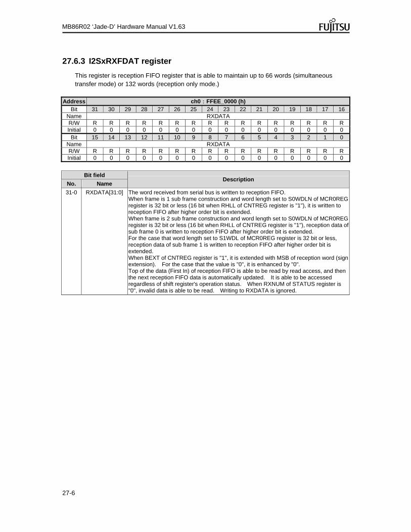
27-6
MB86R02 ‘Jade-D’ Hardware Manual V1.63
27.6.3 I2SxRXFDAT register
This register is reception FIFO register that is able to maintain up to 66 words (simultaneous transfer mode) or 132 words (reception only mode.)
Address ch0:FFEE_0000 (h) Bit 31 30 29 28 27 26 25 24 23 22 21 20 19 18 17 16
Name RXDATA R/W R R R R R R R R R R R R R R R R Initial 0 0 0 0 0 0 0 0 0 0 0 0 0 0 0 0
Bit 15 14 13 12 11 10 9 8 7 6 5 4 3 2 1 0 Name RXDATA R/W R R R R R R R R R R R R R R R R Initial 0 0 0 0 0 0 0 0 0 0 0 0 0 0 0 0
Bit field
Description No. Name
31-0 RXDATA[31:0] The word received from serial bus is written to reception FIFO. When frame is 1 sub frame construction and word length set to S0WDLN of MCR0REG register is 32 bit or less (16 bit when RHLL of CNTREG register is "1"), it is written to reception FIFO after higher order bit is extended. When frame is 2 sub frame construction and word length set to S0WDLN of MCR0REG register is 32 bit or less (16 bit when RHLL of CNTREG register is "1"), reception data of sub frame 0 is written to reception FIFO after higher order bit is extended. For the case that word length set to S1WDL of MCR0REG register is 32 bit or less, reception data of sub frame 1 is written to reception FIFO after higher order bit is extended. When BEXT of CNTREG register is "1", it is extended with MSB of reception word (sign extension). For the case that the value is "0", it is enhanced by "0". Top of the data (First In) of reception FIFO is able to be read by read access, and then the next reception FIFO data is automatically updated. It is able to be accessed regardless of shift register's operation status. When RXNUM of STATUS register is "0", invalid data is able to be read. Writing to RXDATA is ignored.

27-7
MB86R02 ‘Jade-D’ Hardware Manual V1.63
27.6.4 I2SxTXFDAT register
This register is transmission FIFO register that is able to maintain up to 66 words (simultaneous transfer mode) or 132 words (transmission only mode.)
Address ch0:FFEE_0004 (h) Bit 31 30 29 28 27 26 25 24 23 22 21 20 19 18 17 16
Name TXDATA R/W W W W W W W W W W W W W W W W W Initial 0 0 0 0 0 0 0 0 0 0 0 0 0 0 0 0
Bit 15 14 13 12 11 10 9 8 7 6 5 4 3 2 1 0 Name TXDATA R/W W W W W W W W W W W W W W W W W Initial 0 0 0 0 0 0 0 0 0 0 0 0 0 0 0 0
Bit field
Description No. Name
31-0 TXDATA[31:0] Word to be transmitted is able to be written as long as transmission FIFO is not full. Write access is able to be performed regardless of shift register's operation status. The word written to full transmission FIFO is actually not written. Although writing data is accessed in word, half-word, and byte access, actual number of bit to be transmitted is determined by S0WDL and S1WDL (when frame is 2 sub frame) of MCR0REG register. The data read from TXDATA is invalid one (the data after right justified last written data.)

27-8
MB86R02 ‘Jade-D’ Hardware Manual V1.63
27.6.5 I2SxCNTREG register
Address ch0:FFEE_0008 (h)
Bit 31 30 29 28 27 26 25 24 23 22 21 20 19 18 17 16 Name CKRT OVHD R/W R/W R/W R/W R/W R/W R/W R/W R/W R/W R/W R/W R/W R/W R/W R/W R/WInitial 0 0 0 0 0 0 0 0 0 0 0 0 0 0 0 0
Bit 15 14 13 12 11 10 9 8 7 6 5 4 3 2 1 0 Name – MSKB MSMD SBFN RHLL ECKM BEXT FRUN MLSB TXDIS RXDIS SMPL CPOL FSPH FSLN FSPLR/W R R/W R/W R/W R/W R/W R/W R/W R/W R/W R/W R/W R/W R/W R/W R/WInitial 0 0 0 0 0 0 0 0 0 1 1 0 0 0 0 0
Bit field
Description No. Name
31-26 CKRT[5:0] This sets output clock frequency dividing ratio at master operation. AHB clock is divided at ECKM = 0, and external clock is divided at ECKM = 1. Only even number of the ratio is supported and output clock's DUTY becomes 50%. CKRT [5:0] 2 becomes number of AHB clock or external clock cycle included in 1 cycle (I2S_SCKx.) Setting examples are shown below.
External clock mode and external clock are 24.576MHz:
CKRT Dividing ratio
I2S_SCKx
0x00 By pass 24.576MHz
(external clock is output as it is) 0x01 1/2 12.288MHz 0x02 1/4 6.144MHz 0x03 1/6 4.096MHz 0x04 1/8 3.072MHz 0x05 1/10 2.458MHz
: : :
Internal clock mode and AHB clock are 80MHz:
CKRT Dividing ratio
I2S_SCKx
: : : 0x04 1/8 10MHz 0x05 1/10 8MHz 0x06 1/12 6.67MHz 0x07 1/14 5,71MHz 0x08 1/16 5MHz 0x09 1/18 4.44MHz
: : :
25-16 OVHD[9:0] Frame rate is able to be adjusted by inserting OVHD bit following to valid data of the frame. OVHD section of the transmission frame becomes in high impedance. Up to 0 – 1023 OVHD bit is able to be inserted, and is inserted at the end of the frame. The value set to OVHD becomes the number of insertion bit. The following expressions are formed for OVHD and frame synchronous signal cycle (2nd.) 1 sub frame construction: OVHD = Frame synchronous signal cycle/I2S_SCKx cycle – (S0CHL + 1) (S0CHN + 1)2 sub frame construction: OVHD = Frame synchronous signal cycle/I2S_SCKx cycle – (S0CHL + 1) (S0CHN + 1) – (S1CHL + 1) (S1CHN + 1)

27-9
MB86R02 ‘Jade-D’ Hardware Manual V1.63
Bit field Description
No. Name
15 (Reserved) Reserved bits. The write access is ignored. The read value of these bits is always "0".
14 MSKB Serial output data of invalid transmission frame is set. For master operation (MSMD = 1), free-running mode (FRUN = 0), and TXENB = 1: When transmission FIFO is empty at frame synchronous signal output, MSKB is
output to all valid channels of its transmission frame. For slave operation (MSMD = 0) and TXENB = 1: When transmission FIFO is empty at frame synchronous signal reception, MSKB is output to all valid channels of its transmission frame. For the case that transmission word length is shorter than the channel length, MSKB is driven to the rest of bit in transmission channel (channel length -word length.)
13 MSMD Master and slave modes are set.
0 Slave operation
1 Master operation
12 SBFN Sub frame construction (number of sub frame) of the frame is specified.
0 1 sub frame construction (only sub frame 0)
1 2 sub frame construction (sub frame 0 and sub frame 1) Frame starts from the 0th sub frame
11 RHLL Whether word construction of FIFO is 1 or 2 words is set. It is considered to be used at protocol, such as I2S and MSB-Justified.
0 32 bit FIFO word is handled as 1 word
1 32 bit FIFO word is handled as 2 words at serial bus with dividing 16 bit each to low order and high order. They are transferred by serial bus in order of low order, high order, low order, and high order. At reception, 2 consecutive words from serial bus is handled as low order and high order, and they are put in 1 word (32 bit) to write to reception FIFO.
10 ECKM Clock frequency dividing is selected in the master mode.
0 Internal clock (AHB clock) is divided and output
1 External clock (2S_ECLKx pin input) is divided and output
9 BEXT When reception word length is shorter than the word length of FIFO (32 bit when RHLL is "0", and 16 bit when RHLL is "1"), extension mode of upper bit (word length of FIFO -reception word length) should be set.
0 Extended by 0
1 Extended by sign bit (for MSB of word is "1", extended by "1" and its "0" is extended by "0")
8 FRUN Output mode of frame synchronous signal is set.
0 Burst mode When start bit of OPRREG register is "1", frame synchronous signal is output according to TXENB, RXENB, and transmission/reception FIFO conditions
1 Free-running mode When start bit of OPRREG register is "1", frame synchronous signal proceedsfree-running with the set frame rate When start bit is "0", frame synchronous signal is not output.

27-10
MB86R02 ‘Jade-D’ Hardware Manual V1.63
Bit field Description
No. Name
7 MLSB Word bit's shift order is set.
0 Shift starts from MSB of the word
1 Shift starts from LSB of the word
6 TXDIS Transmitting function is enabled or disabled.
0 Transmitting function is enabled
1 Transmitting function is disabled
5 RXDIS Receiving function is enabled or disabled.
0 Receiving function is enabled
1 Receiving function is disabled
4 SMPL Sampling point of the data is specified.
0 Sampling at the center of reception data
1 Sampling at the end of reception data
3 CPOL I2S_SCKx polarity which drives/samples serial data is specified.
0 Data is driven at rising edge of I2S_SCKx, and sampled at falling edge
1 Data is driven at falling edge of I2S_SCKx, and sampled at rising edge
2 FSPH Phase is specified to I2S_WSx frame data.
0 I2S_WSx becomes valid 1 clock before the first bit of frame data
1 I2S_WSx becomes valid at the same time as the first bit of frame data
1 FSLN Pulse width of I2S_WSx is specified.
0 Pulse width is 1 cycle/I2S_SCKx long (1 bit)
1 Pulse width is 1 channel long (1 channel) Setting "1" is prohibited when frame length is 1 channel long.
0 FSPL Polarity of I2S_WSx pin is set.
0 Frame synchronous signal becomes valid with I2S_WSx is "1" The value is "0" at idle
1 Frame synchronous signal becomes valid with I2S_WSx is "0" The value is "1" at idle
Note:
Do not overwrite CNTREG register when start bit of OPRREG register is "1".
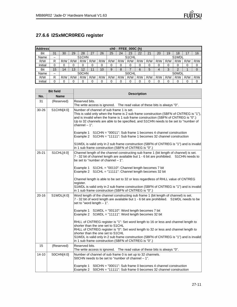
27-11
MB86R02 ‘Jade-D’ Hardware Manual V1.63
27.6.6 I2SxMCR0REG register
Address ch0:FFEE_000C (h)
Bit 31 30 29 28 27 26 25 24 23 22 21 20 19 18 17 16 Name – S1CHN S1CHL S1WDL R/W R R/W R/W R/W R/W R/W R/W R/W R/W R/W R/W R/W R/W R/W R/W R/WInitial 0 0 0 0 0 0 0 0 0 0 0 0 0 0 0 0
Bit 15 14 13 12 11 10 9 8 7 6 5 4 3 2 1 0 Name – S0CHN S0CHL S0WDL R/W R R/W R/W R/W R/W R/W R/W R/W R/W R/W R/W R/W R/W R/W R/W R/WInitial 0 0 0 0 0 0 0 0 0 0 0 0 0 0 0 0
Bit field
Description No. Name
31 (Reserved) Reserved bits. The write access is ignored. The read value of these bits is always "0".
30-26 S1CHN[4:0] Number of channel of sub frame 1 is set. This is valid only when the frame is 2 sub frame construction (SBFN of CNTREG is "1"), and is invalid when the frame is 1 sub frame construction (SBFN of CNTREG is "0".) Up to 32 channels are able to be specified, and S1CHN needs to be set to "number of channel – 1". Example 1 S1CHN = "00011": Sub frame 1 becomes 4 channel construction Example 2 S1CHN = "11111": Sub frame 1 becomes 32 channel construction S1WDL is valid only in 2 sub frame construction (SBFN of CNTREG is "1") and is invalid in 1 sub frame construction (SBFN of CNTREG is "0".)
25-21 S1CHL[4:0] Channel length of the channel constructing sub frame 1 (bit length of channel) is set. 7 - 32 bit of channel length are available but 1 - 6 bit are prohibited. S1CHN needs to be set to "number of channel – 1". Example 1 S1CHL = "00110": Channel length becomes 7 bit Example 2 S1CHL = "11111": Channel length becomes 32 bit Channel length is able to be set to 32 or less regardless of RHLL value of CNTREG register. S1WDL is valid only in 2 sub frame construction (SBFN of CNTREG is "1") and is invalid in 1 sub frame construction (SBFN of CNTREG is "0".)
20-16 S1WDL[4:0] Word length of the channel constructing sub frame 1 (bit length of channel) is set. 7 - 32 bit of word length are available but 1 - 6 bit are prohibited. S1WDL needs to be set to "word length – 1". Example 1 S1WDL = "00110": Word length becomes 7 bit Example 2 S1WDL = "11111": Word length becomes 32 bit RHLL of CNTREG register is "1": Set word length to 16 or less and channel length to shorter than the one set to S1CHL RHLL of CNTREG register is "0": Set word length to 32 or less and channel length to shorter than the one set to S1CHL S1WDL is valid only in 2 sub frame construction (SBFN of CNTREG is "1") and is invalid in 1 sub frame construction (SBFN of CNTREG is "0".)
15 (Reserved) Reserved bits. The write access is ignored. The read value of these bits is always "0".
14-10 S0CHN[4:0] Number of channel of sub frame 0 is set up to 32 channels. S0CHN needs to be set to "number of channel – 1". Example 1 S0CHN = "00011": Sub frame 0 becomes 4 channel construction Example 2 S0CHN = "11111": Sub frame 0 becomes 32 channel construction

27-12
MB86R02 ‘Jade-D’ Hardware Manual V1.63
Bit field Description
No. Name
9-5 S0CHL[4:0] Channel length of the channel constructing sub frame 0 (bit length of channel) is set. 4 - 32 bit of channel length are available but 1 - 6 bit are prohibited. S0CHN needs to be set to "channel length – 1". Example 1 S0CHL = "00110": Channel length becomes 7 bit Example 2 S0CHL = "11111": Channel length becomes 32 bit The channel length can be set to 32 or less regardless of RHLL value of CNTREG register.
4-0 S0WDL[4:0] Word length of the channel constructing sub frame 0 (number of bit in channel) is set. 4 - 32 bit of word length are available but 1-6 bit are prohibited. S0WDL needs to be set to "word length – 1". Example 1 S0WDL = "00110": Word length becomes 7 bit Example 2 S0WDL = "11111": Word length becomes 32 bit RHLL of CNTREG register is "1": Set word length to 16 or less and channel length to shorter than the one set to S0CHL RHLL of CNTREG register is "0": Set word length to 32 or less and channel length to shorter than the one set to S0CHL
27.6.7 I2SxMCR1REG register
This register controls enable and disable functions to each channel of sub frame 0.
Address ch0:FFEE_0010 (h) Bit 31 30 29 28 27 26 25 24 23 22 21 20 19 18 17 16
Name S0CH31
S0CH30
S0CH29
S0CH28
S0CH27
S0CH26
S0CH25
S0CH24
S0CH23
S0CH22
S0CH21
S0CH20
S0CH19
S0CH18
S0CH17
S0CH16
R/W R/W R/W R/W R/W R/W R/W R/W R/W R/W R/W R/W R/W R/W R/W R/W R/WInitial 0 0 0 0 0 0 0 0 0 0 0 0 0 0 0 0
Bit 15 14 13 12 11 10 9 8 7 6 5 4 3 2 1 0
Name S0CH15
S0CH14
S0CH13
S0CH12
S0CH11
S0CH10
S0CH09
S0CH08
S0CH07
S0CH06
S0CH05
S0CH04
S0CH03
S0CH02
S0CH01
S0CH00
R/W R/W R/W R/W R/W R/W R/W R/W R/W R/W R/W R/W R/W R/W R/W R/W R/WInitial 0 0 0 0 0 0 0 0 0 0 0 0 0 0 0 0
Bit field
Description No. Name
31-0 S0CH31-S0CH00 Name (S0CHxx) of each bit indicates channel number xx of sub frame 0 (e.g. S0CH00 bit controls 0th channel of sub frame 0.) Thus, S0CH31 bit controls 31st channel of sub frame 0.
0 The corresponding channel is disabled Transmission/Reception are not performed to the disabled channel
1 The corresponding channel is enabled Transmission/Reception are performed to the enabled channel

27-13
MB86R02 ‘Jade-D’ Hardware Manual V1.63
27.6.8 I2SxMCR2REG register
This register is to control enable and disable functions to each channel of sub frame 1.
Address ch0:FFEE_0014 (h)
Bit 31 30 29 28 27 26 25 24 23 22 21 20 19 18 17 16
Name S1CH31
S1CH30
S1CH29
S1CH28
S1CH27
S1CH26
S1CH25
S1CH24
S1CH23
S1CH22
S1CH21
S1CH20
S1CH19
S1CH18
S1CH17
S1CH16
R/W R/W R/W R/W R/W R/W R/W R/W R/W R/W R/W R/W R/W R/W R/W R/W R/WInitial 0 0 0 0 0 0 0 0 0 0 0 0 0 0 0 0
Bit 15 14 13 12 11 10 9 8 7 6 5 4 3 2 1 0
Name S1CH15
S1CH14
S1CH13
S1CH12
S1CH11
S1CH10
S1CH09
S1CH08
S1CH07
S1CH06
S1CH05
S1CH04
S1CH03
S1CH02
S1CH01
S1CH00
R/W R/W R/W R/W R/W R/W R/W R/W R/W R/W R/W R/W R/W R/W R/W R/W R/WInitial 0 0 0 0 0 0 0 0 0 0 0 0 0 0 0 0
Bit field
Description No. Name
31-0 S1CH31-S1CH00 Name (S1CHxx) of each bit indicates channel number xx of sub frame 1 (e.g. S1CH00 bit controls 0th channel of sub frame 1.) Thus, S1CH31 bit controls 31st channel of sub frame 1. When frame is 1 sub frame construction (SBFN of CNTREG is "0"), this is invalid.
0 The corresponding channel is disabled Transmission/Reception are not performed to the disabled channel
1 The corresponding channel is enabled Transmission/Reception are performed to the enabled channel

27-14
MB86R02 ‘Jade-D’ Hardware Manual V1.63
27.6.9 I2SxOPRREG register
Address ch0:FFEE_0018 (h)
Bit 31 30 29 28 27 26 25 24 23 22 21 20 19 18 17 16
Name (Reserved) RXEN
B (Reserved) TXENB
R/W R R R R R R R R/W R R R R R R R R/WInitial 0 0 0 0 0 0 0 0 0 0 0 0 0 0 0 0
Bit 15 14 13 12 11 10 9 8 7 6 5 4 3 2 1 0 Name (Reserved) start R/W R R R R R R R R R R R R R R R R/WInitial 0 0 0 0 0 0 0 0 0 0 0 0 0 0 0 0
Bit field
Description No. Name
31-25 (Reserved) Reserved bits. The write access is ignored. The read value of these bits is always "0".
24 RXENB Enable/Disable functions of receiving operation is set.
0 Receiving operation is disabled Reception FIFO becomes empty with writing "0" to this bit When RXENB is "0", the data received from serial reception bus is not written to reception FIFO DMA reception channel stops during DMA transfer
1 Receiving operation is enabled
23-17 (Reserved) Reserved bits. The write access is ignored. The read value of these bits is always "0".
16 TXENB Enable/Disable functions of transmitting operation is set.
0 Transmitting operation is disabled Reception FIFO becomes empty with writing "0" to this bit When TXENB is "0", the data written to TXFDAT register from CPU or DMA is not written to transmission FIFO DMA reception channel stops during DMA transfer
1 Transmitting operation is enabled
15-1 (Reserved) Reserved bits. The write access is ignored. The read value of these bits is always "0".
0 start I2S is enabled/disabled.
0 I2S is stop, and internal transmission/reception FIFO becomes empty by writing "0" to this bit
1 I2S is operable Prohibit overwriting CNTREG, MCR0REG, MCR1REG, and MCR2REG registers when Start is "1".
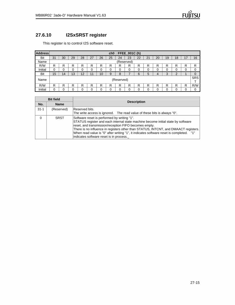
27-15
MB86R02 ‘Jade-D’ Hardware Manual V1.63
27.6.10 I2SxSRST register
This register is to control I2S software reset.
Address ch0:FFEE_001C (h)
Bit 31 30 29 28 27 26 25 24 23 22 21 20 19 18 17 16 Name (Reserved) R/W R R R R R R R R R R R R R R R R Initial 0 0 0 0 0 0 0 0 0 0 0 0 0 0 0 0
Bit 15 14 13 12 11 10 9 8 7 6 5 4 3 2 1 0
Name (Reserved) SRS
T R/W R R R R R R R R R R R R R R R R/WInitial 0 0 0 0 0 0 0 0 0 0 0 0 0 0 0 0
Bit field
Description No. Name
31-1 (Reserved) Reserved bits. The write access is ignored. The read value of these bits is always "0".
0 SRST Software reset is performed by writing "1". STATUS register and each internal state machine become initial state by software reset, and transmission/reception FIFO becomes empty. There is no influence in registers other than STATUS, INTCNT, and DMAACT registers. When read value is "0" after writing "1", it indicates software reset is completed. "1" indicates software reset is in process.

27-16
MB86R02 ‘Jade-D’ Hardware Manual V1.63
27.6.11 I2SxINTCNT register
Address ch0:FFEE_0020 (h)
Bit 31 30 29 28 27 26 25 24 23 22 21 20 19 18 17 16 Name – TXUD1M TBERM FERRM TXUD0M TXOVM TXFDM TXFIM (Reserved) RBERM RXUDM RXOVM EOPM RXFDM RXFIM R/W R R/W R/W R/W R/W R/W R/W R/W R R R/W R/W R/W R/W R/W R/WInitial 0 1 1 1 1 1 1 1 0 0 1 1 1 1 1 1
Bit 15 14 13 12 11 10 9 8 7 6 5 4 3 2 1 0 Name (Reserved) TFTH (Reserved) RPTMR RFTH R/W R R R R R/W R/W R/W R/W R R R/W R/W R/W R/W R/W R/WInitial 0 0 0 0 0 0 0 0 0 0 0 0 0 0 0 0
Bit field
Description No. Name
31 (Reserved) Reserved bits. The write access is ignored. The read value of these bits is always "0".
30 TXUD1M This is transmission FIFO underflow interrupt mask bit. It becomes "1" by software reset.
0 Interrupt to CPU by TXUDR1 of STATUS register is not masked
1 Interrupt to CPU by TXUDR1 of STATUS register is masked
29 TBERM This is interrupt mask bit of block size error of transmission channel. It becomes "1" by software reset.
0 Interrupt to CPU by TBERR of STATUS register is not masked
1 Interrupt to CPU by TBERR of STATUS register is masked
28 FERRM This is frame error interrupt mask bit. It becomes "1" by software reset.
0 Interrupt to CPU by FERR of STATUS register is not masked
1 Interrupt to CPU by FERR of STATUS register is masked.
27 TXUD0M This is transmission FIFO underflow interrupt mask bit. It becomes "1" by software reset.
0 Interrupt to CPU by TXUDR0 of STATUS register is not masked.
1 Interrupt to CPU by TXUDR0 of STATUS register is masked.
26 TXOVM This is transmission FIFO overflow interrupt mask bit. It becomes "1" by software reset.
0 Interrupt to CPU by TXOVM of STATUS register is not masked.
1 Interrupt to CPU by TXOVM of STATUS register is masked.
25 TXFDM This is DMA request mask register bit. It becomes "1" by software reset.
0 DMA transfer is requested when reception data written to transmission FIFO is threshold value or more
1 DMA transfer is not requested even reception data written to transmission FIFO is threshold value or more
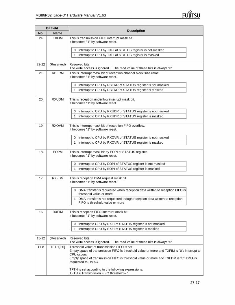
27-17
MB86R02 ‘Jade-D’ Hardware Manual V1.63
Bit field Description
No. Name
24 TXFIM This is transmission FIFO interrupt mask bit. It becomes "1" by software reset.
0 Interrupt to CPU by TXFI of STATUS register is not masked
1 Interrupt to CPU by TXFI of STATUS register is masked
23-22 (Reserved) Reserved bits. The write access is ignored. The read value of these bits is always "0".
21 RBERM This is interrupt mask bit of reception channel block size error. It becomes "1" by software reset.
0 Interrupt to CPU by RBERR of STATUS register is not masked
1 Interrupt to CPU by RBERR of STATUS register is masked
20 RXUDM This is reception underflow interrupt mask bit. It becomes "1" by software reset.
0 Interrupt to CPU by RXUDR of STATUS register is not masked
1 Interrupt to CPU by RXUDR of STATUS register is masked
19 RXOVM This is interrupt mask bit of reception FIFO overflow. It becomes "1" by software reset.
0 Interrupt to CPU by RXOVR of STATUS register is not masked
1 Interrupt to CPU by RXOVR of STATUS register is masked
18 EOPM This is interrupt mask bit by EOPI of STATUS register. It becomes "1" by software reset.
0 Interrupt to CPU by EOPI of STATUS register is not masked
1 Interrupt to CPU by EOPI of STATUS register is masked
17 RXFDM This is reception DMA request mask bit. It becomes "1" by software reset.
0 DMA transfer is requested when reception data written to reception FIFO is threshold value or more
1 DMA transfer is not requested though reception data written to reception FIFO is threshold value or more
16 RXFIM This is reception FIFO interrupt mask bit. It becomes "1" by software reset.
0 Interrupt to CPU by RXFI of STATUS register is not masked
1 Interrupt to CPU by RXFI of STATUS register is masked
15-12 (Reserved) Reserved bits. The write access is ignored. The read value of these bits is always "0".
11-8 TFTH[3:0] Threshold value of transmission FIFO is set. Empty space of transmission FIFO is threshold value or more and TXFIM is "0": Interrupt to CPU occurs Empty space of transmission FIFO is threshold value or more and TXFDM is "0": DMA is requested to DMAC TFTH is set according to the following expressions. TFTH = Transmission FIFO threshold – 1
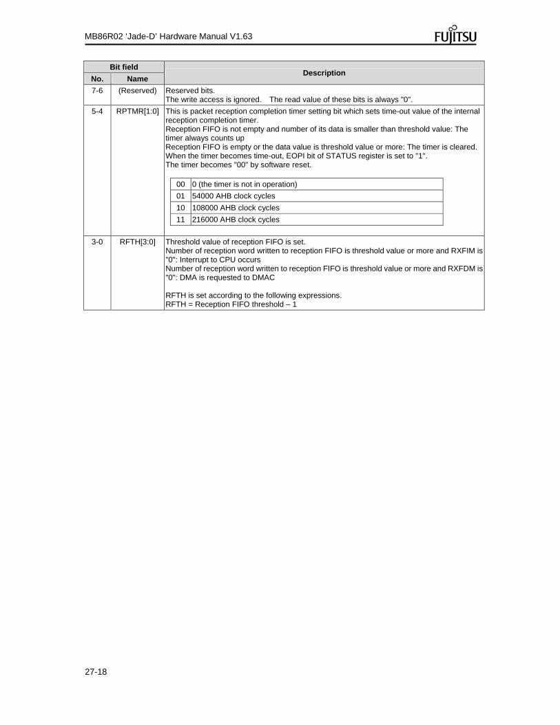
27-18
MB86R02 ‘Jade-D’ Hardware Manual V1.63
Bit field Description
No. Name
7-6 (Reserved) Reserved bits. The write access is ignored. The read value of these bits is always "0".
5-4 RPTMR[1:0] This is packet reception completion timer setting bit which sets time-out value of the internal reception completion timer. Reception FIFO is not empty and number of its data is smaller than threshold value: The timer always counts up Reception FIFO is empty or the data value is threshold value or more: The timer is cleared. When the timer becomes time-out, EOPI bit of STATUS register is set to "1". The timer becomes "00" by software reset.
00 0 (the timer is not in operation)
01 54000 AHB clock cycles
10 108000 AHB clock cycles
11 216000 AHB clock cycles
3-0 RFTH[3:0] Threshold value of reception FIFO is set. Number of reception word written to reception FIFO is threshold value or more and RXFIM is "0": Interrupt to CPU occurs Number of reception word written to reception FIFO is threshold value or more and RXFDM is "0": DMA is requested to DMAC RFTH is set according to the following expressions. RFTH = Reception FIFO threshold – 1

27-19
MB86R02 ‘Jade-D’ Hardware Manual V1.63
27.6.12 I2SxSTATUS register
Address ch0:FFEE_0024 (h)
Bit 31 30 29 28 27 26 25 24 23 22 21 20 19 18 17 16
Name TBERR RBERR FERR TXUDR
1 TXUDR
0 TXOVR RXUDR RXOVR (Reserved) EOPI BSY TXFI RXFI
R/W R R R/W R/W R/W R/W R/W R/W R R R R R/W R R R Initial 0 0 0 0 0 0 0 0 0 0 0 0 0 0 0 0
Bit 15 14 13 12 11 10 9 8 7 6 5 4 3 2 1 0 Name (Reserved) TXNUM (Reserved) RXNUM R/W R R R R R R R R R R R R R R R R Initial 0 0 0 0 0 0 0 0 0 0 0 0 0 0 0 0
Bit field
Description No. Name
31 TBERR In order to set block size of DMA transmission channel to larger value than I2S transmission FIFO threshold to operate, set this bit to "1" and stop the channel. When TBERR is "1" and TBERM of INTCNT register is "0", interrupt to CPU occurs. This becomes "0" by software reset.
30 RBERR In order to set block size of DMA reception channel to larger value than I2S transmission FIFO threshold to operate, set this bit to "1" and stop the channel. When RBERR is "1" and RBERM of INTCNT register is "0", interrupt to CPU occurs. This becomes "0" by software reset.
29 FERR Occurrence of frame error is indicated. This bit is set to "1" in the following cases: Frame synchronous signal is not able to be received with the set frame rate in the
free-running mode (FRUN = 0 of CNTREG) and the slave mode (MSMD = 0 of CNTREG)
The next frame synchronous signal is received during frame transmission/reception in the slave mode (MSMD = 0 of CNTREG), not free-running mode (FRUN = 1 of CNTREG)
When FERR is "1" and FERRM of INTCNT register is "0", interrupt to CPU occurs. Writing "1" from CPU clears the value to "0". This becomes "0" by software reset.
28 TXUDR1 When transmission FIFO underflows at the top of frame, the value is set to "1". Writing "1" from CPU clears the value to "0". This becomes "0" by software reset.
27 TXUDR0 When transmission FIFO underflows during frame transmission (from 2nd bit word to the last frame of the word), the value is set to "1". Writing "1" from CPU clears the value to "0".This becomes "0" by software reset.
26 TXOVR When transmission FIFO overflows, the value is set to "1" indicating transmission data is written in the condition that transmission FIFO is full. The value "1" indicates 1 word or more of transmission data is deleted. When TXOVR is "1" and TXOVM of INTCNT register is "0", interrupt to CPU occurs. Writing "1" from CPU clears the value to "0". This becomes "0" by software reset.
25 RXUDR When reception FIFO underflows, the value is set to "1" indicating read access is carried out to reception FIFO in the condition that reception FIFO is empty. Writing "1" from CPU clears the value to "0". This becomes "0" by software reset.
24 RXOVR When reception FIFO overflows, the value is set to "1" indicating reception is carried out in the condition that reception FIFO is full. The value "1" indicates 1 word or more of reception data is deleted. When RXOVR is "1" and RXOVM of INTCNT register is "0", interrupt to CPU occurs. Writing "1" from CPU clears the value to "0". This becomes "0" by software reset.
23-20 (Reserved) Reserved bits. The write access is ignored. The read value of these bits is always "0".

27-20
MB86R02 ‘Jade-D’ Hardware Manual V1.63
Bit field Description
No. Name
19 EOPI This is interrupt flag containing reception timer. The timer is enabled when following conditions are met at the same time: RXDIS of CNTREG register is set to "0" RXFDM of INTCNT register is set to "0" MSMD of CNTREG register is set to "0" start bit of OPRREG register is set to "1" and RXENB = "1"
After the reset, operation starts with the 1st word reception. Then the value is cleared every time word is received. When reception FIFO is not empty at the time set to RPTMR of INTCNT register, the value is set to "1". When EOPI is "1" and EOPM of INTCNT register is "0", interrupt to CPU occurs. The value is automatically cleared if reception FIFO data is threshold or more, or it becomes empty. Writing "1" from CPU clears the value to "0". This becomes "0" by software reset.
18 BSY Serial transmission control part is busy state. This bit is not affected by software reset.
0 Serial transmission control part is in idle
1 Serial transmission control part is in busy
17 TXFI When empty slot of transmission FIFO is larger than the threshold set in TFTH of INTCNT register, this bit is set to "1". This bit is "1" and TXFIM bit of INTCNT register is "0": Interrupt to CPU occurs This bit is "1" and TXFDM bit of INTCNT register is "0": DMA is requested When number of empty slot of reception FIFO becomes smaller than the threshold by writing to TXFDAT register from CPU or DMAC, this bit is cleared automatically to "0". The value is also become "0" when start bit of start register is "0" and TXENB bit of OPRREG register is "0". If software reset is performed at start bit = "1" and TXENB bit = "1", the value becomes "0" during software reset then changes to "1" after the process.
16 RXFI When number of reception FIFO data is larger than the threshold set in RFTF of INTCNT register, this bit is set to "1". This bit is "1" and RXFIM bit of INTCNT register is "0": Interrupt to CPU occurs This bit is "1" and RXFDM bit of INTCNT register is "0": DMA is requested When number of data in reception FIFO becomes smaller than the threshold by reading RXFDAT register from CPU or DMAC, this bit is automatically cleared to "0". When start bit of start register is "0" or RXENB bit of OPRREG register is "0", this bit becomes "0". This becomes "0" by software reset.
15-14 (Reserved) Reserved bits. The write access is ignored. The read value of these bits is always "0".
13-8 TXNUM[5:0] The number of data in transmission FIFO is indicated. This bit is incremented by write access to TXFDAT register and decremented by serial word transfer. Max. value of 66 can be displayed in the simultaneous transfer mode, and value of 132 in the transmission only mode. This becomes "0" by software reset.
7-6 (Reserved) Reserved bits. The write access is ignored. The read value of these bits is always "0".
5-0 RXNUM[5:0] The number of data in reception FIFO is indicated. This bit is incremented by word reception from serial bus and decremented by read access to RXFDAT register. Max. values of 66 can be displayed in the simultaneous transfer mode, and value of 132 in the reception mode. This becomes "0" by software reset.
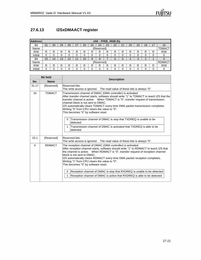
27-21
MB86R02 ‘Jade-D’ Hardware Manual V1.63
27.6.13 I2SxDMAACT register
Address ch0:FFEE_0028 (h)
Bit 31 30 29 28 27 26 25 24 23 22 21 20 19 18 17 16 Name (Reserved) TDMACTR/W R R R R R R R R R R R R R R R R/W Initial 0 0 0 0 0 0 0 0 0 0 0 0 0 0 0 0
Bit 15 14 13 12 11 10 9 8 7 6 5 4 3 2 1 0 Name (Reserved) RDMACTR/W R R R R R R R R R R R R R R R R/W Initial 0 0 0 0 0 0 0 0 0 0 0 0 0 0 0 0
Bit field
Description No. Name
31-17 (Reserved) Reserved bits. The write access is ignored. The read value of these bits is always "0".
16 TDMACT Transmission channel of DMAC (DMA controller) is activated. After transfer channel starts, software should write "1" to TDMACT to teach I2S that the transfer channel is active. When TDMACT is "0", transfer request of transmission channel block is not sent to DMAC. I2S automatically clears TDMACT every time DMA packet transmission completes. Writing "0" from CPU clears the value to "0". This becomes "0" by software reset.
0 Transmission channel of DMAC is stop that TXDREQ is unable to be detected
1 Transmission channel of DMAC is activated that TXDREQ is able to be detected
15-1 (Reserved) Reserved bits. The write access is ignored. The read value of these bits is always "0".
0 RDMACT The reception channel of DMAC (DMA controller) is activated. After reception channel starts, software should write "1" to RDMACT to teach I2S that the channel is active. When RDMACT is "0", transfer request of reception channel block is not sent to DMAC. I2S automatically clears RDMACT every time DMA packet reception completes. Writing "1" from CPU clears the value to "0". This becomes "0" by software reset.
0 Reception channel of DMAC is stop that RXDREQ is unable to be detected
1 Reception channel of DMAC is active that RXDREQ is able to be detected
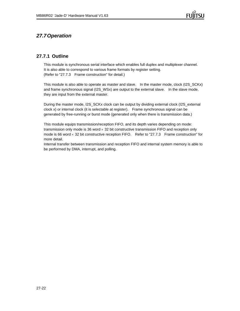
27-22
MB86R02 ‘Jade-D’ Hardware Manual V1.63
27.7 Operation
27.7.1 Outline
This module is synchronous serial interface which enables full duplex and multiplexer channel. It is also able to correspond to various frame formats by register setting. (Refer to "27.7.3 Frame construction" for detail.) This module is also able to operate as master and slave. In the master mode, clock (I2S_SCKx) and frame synchronous signal (I2S_WSx) are output to the external slave. In the slave mode, they are input from the external master. During the master mode, I2S_SCKx clock can be output by dividing external clock (I2S_external clock x) or internal clock (it is selectable at register). Frame synchronous signal can be generated by free-running or burst mode (generated only when there is transmission data.) This module equips transmission/reception FIFO, and its depth varies depending on mode: transmission only mode is 36 word 32 bit constructive transmission FIFO and reception only mode is 66 word 32 bit constructive reception FIFO. Refer to "27.7.3 Frame construction" for more detail. Internal transfer between transmission and reception FIFO and internal system memory is able to be performed by DMA, interrupt, and polling.

27-23
MB86R02 ‘Jade-D’ Hardware Manual V1.63
27.7.2 Transfer start, stop, and malfunction
Transmission only mode Transfer setting
Operation Master mode (MSMD = 1) Slave mode (MSMD = 0)
Transmission only TXDIS = 0 RXDIS = 1
Start Free-running mode (FRUN = 1): After start bit becomes "1" and TXENB bit is "1", frame synchronous signal starts to output when transmission FIFO is not empty. From the 2nd time, it outputs frame synchronous signal with the frame rate determined by the register setting. If transfer FIFO is empty, empty frame is output at the same time of frame synchronous signal output. Serial data of the empty frame is able to be set to "0" or "1" by the register setting.
Burst mode (FRUN = 0): When start bit is "1" and TXENB bit is "1", frame synchronous signal is output if transfer FIFO is not empty. Always confirm transmission FIFO status at the end of 1 frame output or at idle to output the signal if transfer FIFO is not empty.
Free-running mode (FRUN = 1): The frame rate determined by the register setting inputs frame synchronous signal. If transmission FIFO is empty at inputting frame synchronous signal with start bit is "1" and TXENB bit is "1", empty frame is output. Serial data of the empty frame is able to be set to "0" or "1" by the register setting.
Burst mode (FRUN=0): When start bit is "1" and TXENB bit is "1", 1 frame is output every time frame synchronous signal is input. When transmission FIFO is empty at the time of frame synchronous signal input, empty frame is output.
Stop At the time of stop, transmission FIFO becomes empty with having no data transfer from internal memory to I2S transmission FIFO.
To maintain start bit to "1" TXENB = "1": Keep outputting frame synchronous signal in the free-running mode. When transmission FIFO becomes empty, empty frame is output; however do not output frame synchronous signal in the burst mode. Output empty frame bit to serial data bus. TXENB = "0": When "0" is written to TXENB, transmission FIFO becomes empty that the data in the FIFO at writing "0" is not sent. Although frame synchronous signal continues outputting in the free-running mode, serial bus becomes in high impedance state. In the burst mode, frame synchronous signal is not output and serial data bus becomes in high impedance state.
To make start bit "0" Write "0" to start bit, then transmission FIFO becomes empty. Stop clock supply to the serial control part regardless of TXENB setting, and do not output clock to external part. Frame synchronous signal output should also be stopped. Serial data bus becomes in high impedance state.
To maintain start bit to "1" TXENB = "1":
Output empty frame data to serial bus.
TXENB = "0": Write "0" to TXENB, then transmission FIFO becomes empty that the data in the FIFO at writing "0" is not sent. Data writing to transmission FIFO and transmission frame detection are stop. Serial data bus becomes in high impedance state.
To make start bit "0" Write "0" to start bit, then transmission FIFO becomes empty. Writing to transmission FIFO and detection of transmission frame synchronous signal are stop regardless of TXENB setting.
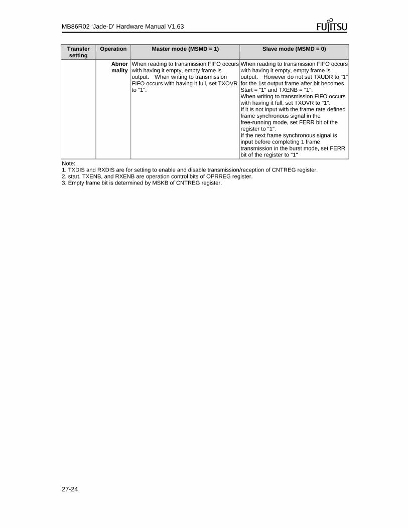
27-24
MB86R02 ‘Jade-D’ Hardware Manual V1.63
Transfer setting
Operation Master mode (MSMD = 1) Slave mode (MSMD = 0)
Abnormality
When reading to transmission FIFO occurs with having it empty, empty frame is output. When writing to transmission FIFO occurs with having it full, set TXOVR to "1".
When reading to transmission FIFO occurs with having it empty, empty frame is output. However do not set TXUDR to "1"for the 1st output frame after bit becomes Start = "1" and TXENB = "1". When writing to transmission FIFO occurs with having it full, set TXOVR to "1". If it is not input with the frame rate defined frame synchronous signal in the free-running mode, set FERR bit of the register to "1". If the next frame synchronous signal is input before completing 1 frame transmission in the burst mode, set FERR bit of the register to "1"
Note: 1. TXDIS and RXDIS are for setting to enable and disable transmission/reception of CNTREG register. 2. start, TXENB, and RXENB are operation control bits of OPRREG register. 3. Empty frame bit is determined by MSKB of CNTREG register.

27-25
MB86R02 ‘Jade-D’ Hardware Manual V1.63
Reception only mode Transfer setting
Operation Master mode (MSMD = 1) Slave mode (MSMD = 0)
Reception only
TXDIS = 1 RXDIS = 0
Start Free-running mode (FRUN = 1):Frame synchronous signal starts to output after start bit becomes "1" and TXENB bit is "1" when transmission FIFO is not empty. From the 2nd time, output frame synchronous signal with the frame rate determined by the register setting.
Burst mode (FRUN = 0): When start bit is "1" and RXENB bit is "1", output frame synchronous signal to receive frame if reception FIFO is not full. If the FIFO is full, the signal does not output.
Free-running mode (FRUN = 1):When start bit is "1" and RXENB bit is "1", input frame synchronous signal with the frame rate determined by the register setting. Frame should be received every time the signal is input.
Burst mode (FRUN = 0): When start bit is "1" and RXENB bit is "1", perform frame reception every time frame synchronous signal is input. The signal is input with less speed than the frame rate in the free-running mode.
Stop At the time of stop, frame is not imported from serial bus even though reception FIFO is empty in the condition that data transfer from I2S reception FIFO to internal memory is not required.
To maintain start bit to "1" Write "0" to RXENB and empty reception FIFO. Although frame synchronous signal is kept outputting in the free-running mode, frame is not received. In the burst mode, frame is not received and the signal is not output.
To make start bit "0" Write "0" to start bit, then reception FIFO becomes empty. Clock supply to the serial control part stops regardless of RXENB setting, and I2S_SCKx supply to the external part is stop as well.
To maintain start bit to "1"Reception FIFO becomes empty by "0" writing to RXENB. Ignore the input frame synchronous signal, and do not receive the frame.
To make the start bit "0" Write "0" to the start bit, then reception FIFO becomes empty. Ignore the input frame synchronous signal regardless of RXENB setting, and do not receive the frame.
Abnormality When writing to reception FIFO occurs with having it full, set RXOVR to "1". The bit also should be set to "1" when read access to reception FIFO occurs with having it empty.
When writing to reception FIFO occurs with having it full, set RXOVR of the STATUS register to "1". When read access to reception FIFO occurs with having it empty, set RXUDR of the register to "1". Free-running mode: If frame synchronous signal is not input with the frame rate defined by the register setting, set FERR bit of the register to "1". Burst mode: Set the bit also to "1" if the next frame synchronous signal is input during 1 frame reception.
Note: 1. TXDIS and RXDIS are for setting to enable and disable transmission/reception of CNTREG register. 2. start, TXENB, and RXENB are operation control bits of OPRREG register.

27-26
MB86R02 ‘Jade-D’ Hardware Manual V1.63
Simultaneous transfer mode Transfer setting Operation Master mode (MSMD = 1) Slave mode (MSMD = 0)
Simultaneous transfer
TXDIS = 0 RXDIS = 0
Start Free-running mode (FRUN = 1):
Status of Start = 1, TXENB = 1, and RXENB = 1: The same operation as
transmission only mode. Status of Start = 1, TXENB = 0, and RXENB = 1: The same operation as reception
only mode. Status of Start = 1, TXENB = 1, and RXENB = 1: Frame synchronous signal is
output from the state that transmission FIFO is not empty and reception FIFO is not full. Then output frame synchronous signal with the frame rate defined by the register setting; at the same time, output empty frame if reception FIFO is empty.
Empty frame's serial data is able to be set to "0" or "1" at the register setting. Every time frame synchronous signal is output, receive frame.
Burst mode (FRUN = 0): Status of Start = 1, TXENB = 1, and RXENB = 0: The same operation as
transmission only mode. Status of Start = 1, TXENB = 0, and RXENB = 1: The same operation as reception
only mode. Status of Start = 1, TXENB = 1, and RXENB = 1: Frame synchronous signal is
output from the state that transmission FIFO is not empty and reception FIFO is not full.
After completion of 1 frame output or at idle state, always confirm transmission/reception FIFO status. If transmission FIFO is not empty and reception FIFO is not full, output frame synchronous signal to perform frame transmission/reception.
Free-running mode (FRUN = 1):
Status of Start = 1, TXENB = 1, and RXENB = 0: The same operation as
transmission only mode. Status of Start = 1, TXENB = 0, and RXENB = 1: The same operation as reception only mode. Status of Start = 1, TXENB = 1, and RXENB = 1: Frame synchronous signal is input
with the frame rate defined by the register setting; at the same time, output empty frame if transmission FIFO is empty. Its serial data is able to be set to "0" or "1" at the register setting. Every time frame synchronous signal is input, receive frame.
Burst mode (FRUN = 0):
Every time frame synchronous signal is input with start bit is "1", transmission and reception for 1 frame is performed. When the signal is input, output empty frame if transmission FIFO is empty.

27-27
MB86R02 ‘Jade-D’ Hardware Manual V1.63
Transfer setting Operation Master mode (MSMD = 1) Slave mode (MSMD = 0)
Stop Stop operation has following states:Transmission stop: Transmission FIFO becomes empty without sending data from internal memory to I2S transmission FIFO. Reception stop: Data does not need to be transferredfrom I2S reception FIFO to internal memory.
To maintain start bit to "1" Keep outputting frame synchronous signal in the free-running mode. In the burst mode, do not output the signal when transmission FIFO becomes empty. Transmission stop: TXENB = 1: Keep outputting empty frame bit when transmission FIFO becomes empty. TXENB = 0: Transmission FIFO becomes empty and transmission serial data bus becomes in high impedance. Do not send the data in transmission FIFO at writing "0" to TXENB. Writing to transmission FIFO stops. Reception stop: Write "0" to RXENB, then reception FIFO becomes empty and frame reception operation stops.
To make start bit "0"
Write "0" to start bit, then transmission/reception FIFO becomes empty. The clock supply to the internal serial control part stops regardless of TXENB and RXENB statuses as well as I2S_SCKX output to the external part and frame synchronoussignal output.
To maintain start bit to "1" Transmission stop: Keep outputting empty frame bit after transmission FIFO becomes empty in order to maintain this bit to TXENB = 1. When the value is changed to "0", transmission FIFO becomes empty and transmission serial data bus becomes in high impedance. Do not send the data in transmission FIFO at writing "0" to TXENB. Stop writing to transmission FIFO. Reception stop: Write "0" to RXENB, then reception FIFO becomes empty and frame reception operation stops.
To make start bit "0" Write "0" to start bit, then transmission/reception FIFO becomes empty. Stop transmission/reception regardless of TXENB and RXENB statuses.
Abnormality When reading to transmission FIFO occurs with having it empty, output empty frame bit. When writing to transmission FIFO occurs with having it full, set TXOVR to "1". If read access to reception FIFO occurs while it is empty, set RXUDR of STATUS register to "1". If writing to reception FIFO occurs with having it full, set RXOVR of the register to "1".
When reading to transmission FIFO occurs with having it empty, output empty frame bit. When writing to transmission FIFO occurs with having it full, set TXOVR to "1". When read access occurs to reception FIFO with having it empty, set RXUDR of STATUS register to "1". When writing to reception FIFO occurs with having it full, set RXOVR of the register to "1". If it is not input with the frame rate defined frame synchronous signal in the free-running mode, set FERR bit of the register to "1". If the next frame synchronous signal is input before completing 1 frame transmission in the burst mode, set FERR bit of the register to "1".

27-28
MB86R02 ‘Jade-D’ Hardware Manual V1.63
Transfer setting Operation Master mode (MSMD = 1) Slave mode (MSMD = 0)
Note: 1. TXDIS and RXDIS are for setting to enable and disable transmission/reception of CNTREG register. 2. start, TXENB, and RXENB are operation control bits of OPRREG register. 3. Empty frame bit is determined by MSKB of CNTREG register.

27-29
MB86R02 ‘Jade-D’ Hardware Manual V1.63
27.7.3 Frame construction
This module supports frame format of multiplexer channel construction. Frame is able to be set to 1 or 2 sub frames; moreover, number of each frame’s channel and word length are able to be set individually.
27.7.3.1 1 sub frame construction
One Frame with one Sub frame
One Sub frame(1-32 channels)
Channel-0(7-32 bit) Channel-1(7-32 bit) Channel-n(7-32 bit) Over-Head(0-1023 bit)
0-1 bit
1 bit Channel-length bit
I2S_SCKx
I2S_WSx(FSLN=0)
I2S_WSx(FSLN=1)
I2S_SDIxI2S_SDOx
Figure 27-2 1 sub frame composite frame
Description 1. When SBFN bit of CNTREG register is "0", frame becomes 1 sub frame composite.
2. Number of channel of 1 sub frame is determined by S0CHN of MC0REG register. Up to 32 channels are settable.
3. Each channel bit length (word length) is determined by S0WDL of MC0REG register.
4. Sub frame channel starts from 0th, and each channel is settable to valid/invalid with the corresponding bit of MC1REG register. Transmission/Reception of data is not performed to invalid channel.
5 Dummy bit can be inserted behind sub frame by setting OVHD of CNTREG register. 0-1023 bit are insertable.
6. Polarity of I2S_WSx is set with FSPL bit of CNTREG register.
7. Pulse width of I2S_WSx can be set to 1 bit or 1 word length by setting FSLN bit of CNTREG register.
8. Timing from the edge I2S_WSx becomes valid to the first bit of frame is settable to "0" or "1" bit.
9. In this construction, setting of S1CHN of MC0REG register, S1WDL register and MC2REG register are ignored.

27-30
MB86R02 ‘Jade-D’ Hardware Manual V1.63
27.7.3.2 2 sub frame construction
Over-head(0-1023 bit)
0-1 bit
1 bit
I2S_SCKx
I2S_WSx (FSLN = 0)
I2S_WSx (FSLN = 1)
I2S_SDIx/SDOx
One frame with two sub frames
Sub frame #0 (1-32 channels) Sub frame #1 (1-32 channels)
Channel-0 (7-32 bit) of sub frame #0
Channel-n (7-32 bit) of sub frame #0
Channel-0 (7-32 bit) of sub frame #1
Channel-n (7-32 bit) of sub frame #1
Figure 27-3 2 sub frame composite frame
Description
1. When SBFN bit of CNTREG register is "1", frame becomes 2 sub frame composite that first sub frame is 0 and the next one is 1.
2. Set number of channel of sub frame 0 to S0CHN of MC0REG register, and set number of sub frame 1 channel to S1CHN of the register. Those numbers of channel are individual that they do not need to have the same channel. Up to 32 channels are settable.
3. Channel bit length (word length) of sub frame 0 is determined by S0WDL of MC0REG register. For sub frame 1, they are determined by S1WDL of MC0REG register. Since channel bit length of the sub frame is individual, those channels (word length) do not need to be the same.
4. Sub frame channel starts from 0th. Each channel of sub frame 0 is settable to valid/invalid with the corresponding bit of MC1REG register, and corresponding bit of MC2REG register for sub frame 1. Transmission/Reception of data is not performed to invalid channel.
5 Dummy bit can be inserted behind sub frame 1 by setting OVHD of CNTREG. 0-1023 bit are insertable.
6. Polarity of I2S_WSx is set to FSPL bit of CNTREG register.
7. Pulse width of I2S_WSx can be set to 1 bit or 1 channel length by setting FSLN bit of CNTREG register. Channel length setting of 1 channel is determined by the channel length of sub frame 0.
8. Timing from the edge I2S_WSx becomes valid to the first bit of frame is settable to "0" or "1" bit.
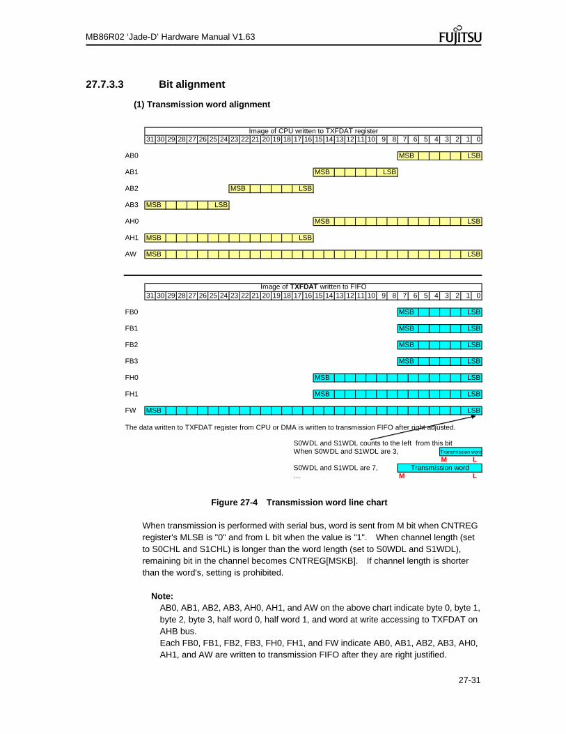
27-31
MB86R02 ‘Jade-D’ Hardware Manual V1.63
27.7.3.3 Bit alignment
(1) Transmission word alignment
Figure 27-4 Transmission word line chart
When transmission is performed with serial bus, word is sent from M bit when CNTREG register's MLSB is "0" and from L bit when the value is "1". When channel length (set to S0CHL and S1CHL) is longer than the word length (set to S0WDL and S1WDL), remaining bit in the channel becomes CNTREG[MSKB]. If channel length is shorter than the word's, setting is prohibited.
Note:
AB0, AB1, AB2, AB3, AH0, AH1, and AW on the above chart indicate byte 0, byte 1, byte 2, byte 3, half word 0, half word 1, and word at write accessing to TXFDAT on AHB bus. Each FB0, FB1, FB2, FB3, FH0, FH1, and FW indicate AB0, AB1, AB2, AB3, AH0, AH1, and AW are written to transmission FIFO after they are right justified.
31 30 29 28 27 26 25 24 23 22 21 20 19 18 17 16 15 14 13 12 11 10 9 8 7 6 5 4 3 2 1 0
AB0 MSB LSB
AB1 MSB LSB
AB2 MSB LSB
AB3 MSB LSB
AH0 MSB LSB
AH1 MSB LSB
AW MSB LSB
31 30 29 28 27 26 25 24 23 22 21 20 19 18 17 16 15 14 13 12 11 10 9 8 7 6 5 4 3 2 1 0
FB0 MSB LSB
FB1 MSB LSB
FB2 MSB LSB
FB3 MSB LSB
FH0 MSB LSB
FH1 MSB LSB
FW MSB LSB
S0WDL and S1WDL counts to the left from this bitWhen S0WDL and S1WDL are 3,
M LS0WDL and S1WDL are 7,… M L
Image of CPU written to TXFDAT register
Image of TXFDAT written to FIFO
Transmission word
Transmission word
The data written to TXFDAT register from CPU or DMA is written to transmission FIFO after right adjusted.

27-32
MB86R02 ‘Jade-D’ Hardware Manual V1.63
(2) Reception word alignment
Figure 27-5 Reception word line chart This chart shows word line example of when word length is 8. The word received from serial bus is always written to reception FIFO after right-justified. Therefore, read access should be performed from AHB bus to RXFDAT in order to read as follows:
Word length 8 or less: Byte 0 9 – 16: Half word 0 17 – 32: All words.
31 30 29 28 27 26 25 24 23 22 21 20 19 18 17 16 15 14 13 12 11 10 9 8 7 6 5 4 3 2 1 0RXFDAT
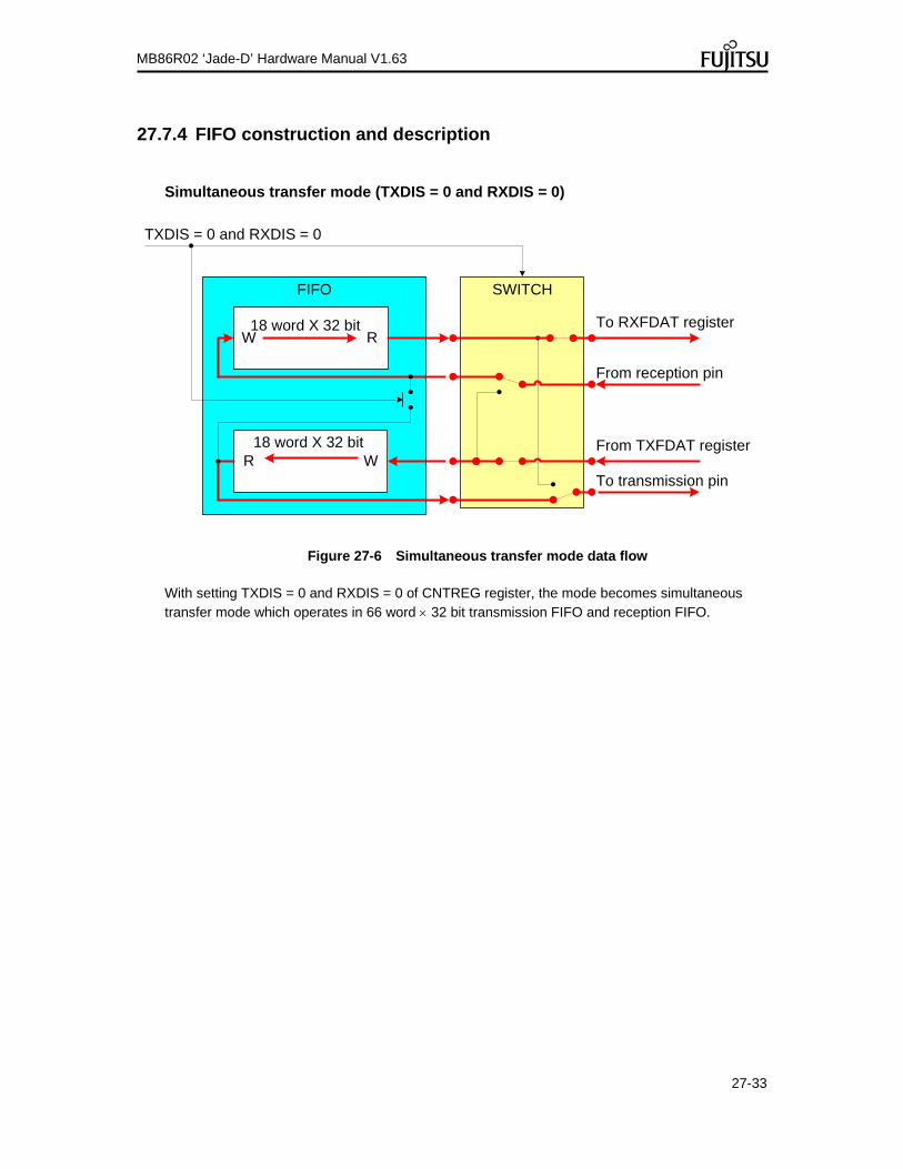
27-33
MB86R02 ‘Jade-D’ Hardware Manual V1.63
27.7.4 FIFO construction and description
Simultaneous transfer mode (TXDIS = 0 and RXDIS = 0)
SWITCHFIFO
W R
From reception pin
To RXFDAT register
R WFrom TXFDAT register
To transmission pin
TXDIS = 0 and RXDIS = 0
18 word X 32 bit
18 word X 32 bit
Figure 27-6 Simultaneous transfer mode data flow With setting TXDIS = 0 and RXDIS = 0 of CNTREG register, the mode becomes simultaneous transfer mode which operates in 66 word 32 bit transmission FIFO and reception FIFO.

27-34
MB86R02 ‘Jade-D’ Hardware Manual V1.63
Transmission only mode (TXDIS = 0 and RXDIS = 1)
SWITCHFIFO
W R
R W
To RXFDAT register
From TXFDAT register
From reception pin
To transmission pin
TXDIS = 0 and RXDIS = 1
18 word X 32 bit
18 word X 32 bit
Figure 27-7 Transmission only mode data flow With setting TXDIS = 0 and RXDIS = 1 of CNTREG register, the mode becomes transmission only mode which operates in 36 word 32 bit transmission FIFO, and reception is not performed.
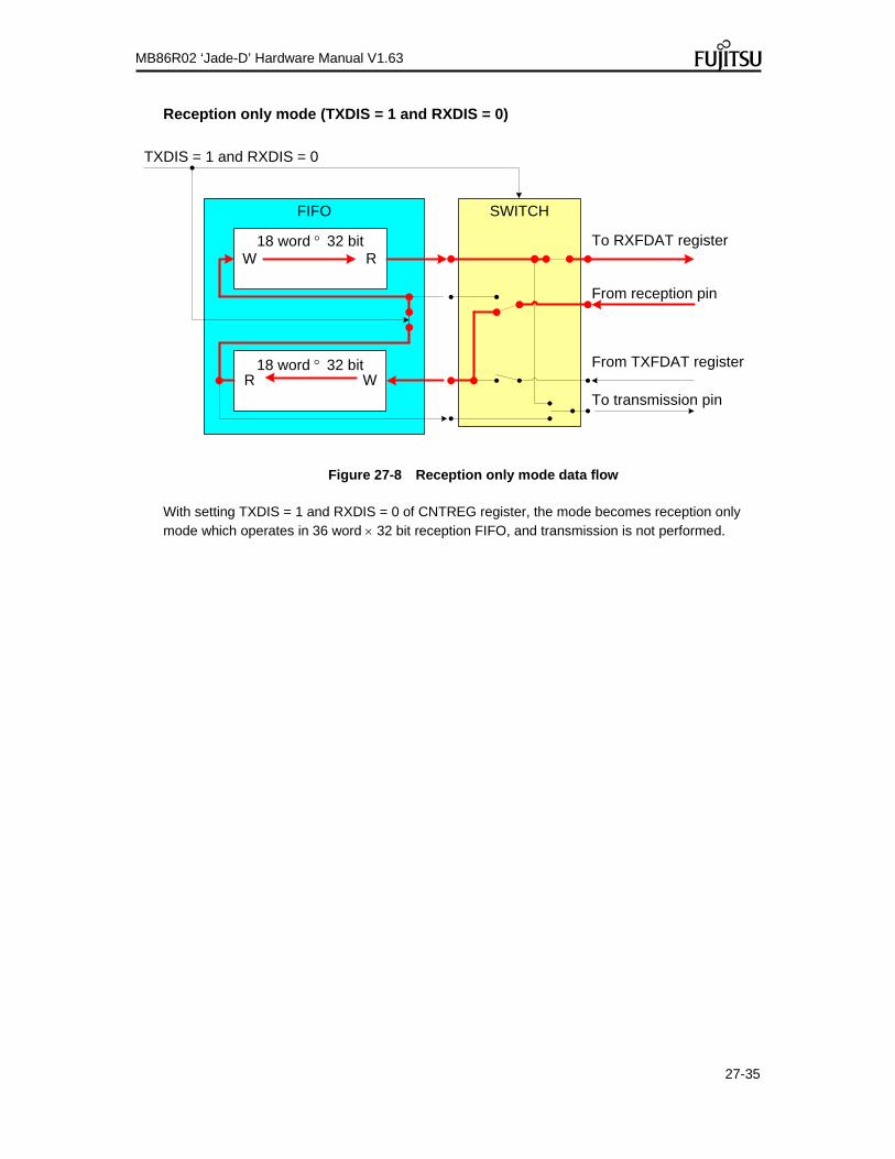
27-35
MB86R02 ‘Jade-D’ Hardware Manual V1.63
Reception only mode (TXDIS = 1 and RXDIS = 0)
SWITCHFIFO
W R
R W
TXDIS = 1 and RXDIS = 0
To RXFDAT register
From TXFDAT register
From reception pin
To transmission pin
18 word 32 bit
18 word 32 bit
Figure 27-8 Reception only mode data flow With setting TXDIS = 1 and RXDIS = 0 of CNTREG register, the mode becomes reception only mode which operates in 36 word 32 bit reception FIFO, and transmission is not performed.

28-1
MB86R02 ‘Jade-D’ Hardware Manual V1.63
28 UART Interface This chapter describes function and operation of the UART interface.
28.1 Outline
UART is asynchronous transmission/reception serial interface which is controllable by software. This LSI incorporates 6 UART modules.
28.2 Feature
UART has following features: Programmable baud rate (baud rate is selectable arbitrarily based on APB clock) 16 byte transmission FIFO and 16 byte reception FIFO
28.3 Block diagram
Figure 28-1 shows block diagram of UART.
IRC_A
DMAC
Baud rate generator
Register
Transmitter
FIFO shift
Modem I/F CPU I/F
Receiver FIFO shift
INTR
XTXRDY
XRXRDY
UART_SOUT0
UART_XRTS0
UART_SIN0
UART_XCTS0
APB bus
UART ch5
UART ch0
UART_SOUT5
UART_SIN5
MB86R02
UART ch1 UART_SOUT1
UART_SIN1
Figure 28-1 Block diagram of UART

28-2
MB86R02 ‘Jade-D’ Hardware Manual V1.63
28.4 Related pin
UART uses the following pins.
Pin Direction Qty. Description
UART_SIN0 UART_SIN1 UART_SIN2 UART_SIN3 UART_SIN4 UART_SIN5
IN 6 Input pin of serial data. The umber at the end of pin shows channel number of UART.
UART_SOUT0 UART_SOUT1 UART_SOUT2 UART_SOUT3 UART_SOUT4 UART_SOUT5
OUT 6 Output pin of serial data. The number at the end of pin shows channel number of UART.
UART_XCTS0 IN 1 Input pin of modem control signal, CLEAR TO SEND. Only channel 0 of UART has this pin.
UART_XRTS0 OUT 1 Output pin of modem control signal, REQUEST TO SEND Only channel 0 of UART has this pin.
28.5 Supply clock
APB clock is supplied to UART. Refer to "5. Clock reset generator (CRG)" for frequency setting and control specification of the clock.

28-3
MB86R02 ‘Jade-D’ Hardware Manual V1.63
28.6 Registers
This section describes UART interface module's registers.
28.6.1 Register list
The LSI has 6 UART channels (please note that some are only available via pin multiplex settings). Each module has the registers shown in Table 28-1.
Table 28-1 UART register list Channel Address Register Description
UART ch0 FFFE1000h URT0RFR Reception FIFO register (read only) that is valid in DLAB = 0
URT0TFR Transmission FIFO register (write only) that is valid in DLAB = 0
URT0DLL Divider latch (low order byte) register that is valid in DLAB = 1
FFFE1004h URT0IER Interrupt enable that is valid in DLAB = 0.
URT0DLM Divider latch (high order byte) register that is valid in DLAB = 1
FFFE1008h URT0IIR Interrupt ID register (read only)
URT0FCR FIFO control (write only)
FFFE100Ch URT0LCR Line control register
FFFE1010h URT0MCR Modem control register
FFFE1014h URT0LSR Line status register (read only)
FFFE1018h URT0MSR Modem status register (read only)
UART ch1 FFFE2000h URT1RFR Reception FIFO register (read only) that is valid in DLAB = 0
URT1TFR Transmission FIFO register (write only) that is valid in DLAB = 0
URT1DLL Divider latch register (low order byte) that is valid in DLAB = 1
FFFE2004h URT1IER Interrupt enable that is valid in DLAB = 0.
URT1DLM Divider latch (high order byte) register that is valid in DLAB = 1
FFFE2008h URT1IIR Interrupt ID register (read only)
URT1FCR FIFO control (write only)
FFFE200Ch URT1LCR Line control register
FFFE2010h URT1MCR Modem control register
FFFE2014h URT1LSR Line status register (read only)
FFFE2018h
URT1MSR
Modem status register (read only)
UART ch2 FFF50000h URT2RFR Reception FIFO register (read only) that is valid in DLAB = 0
URT2TFR Transmission FIFO register (write only) that is valid in DLAB = 0
URT2DLL Divider latch (low order byte) register that is valid in DLAB = 1
FFF50004h URT2IER Interrupt enable that is valid in DLAB = 0.
URT2DLM Divider latch (high order byte) register that is valid in DLAB = 1
FFF50008h URT2IIR Interrupt ID register (read only)
URT2FCR FIFO control (write only)
FFF5000Ch URT2LCR Line control register
FFF50010h URT2MCR Modem control register
FFF50014h URT2LSR Line status register (read only)
FFF50018h URT2MSR Modem status register (read only)
UART ch3 FFF51000h URT3RFR Reception FIFO register (read only) that is valid in DLAB = 0
URT3TFR Transmission FIFO register (write only) that is valid in DLAB = 0

28-4
MB86R02 ‘Jade-D’ Hardware Manual V1.63
Channel Address Register Description
URT3DLL Divider latch (low order byte) register that is valid in DLAB = 1
UART ch3 FFF51004h URT3IER Interrupt enable that is valid in DLAB = 0.
URT3DLM Divider latch (high order byte) register that is valid in DLAB = 1
FFF51008h URT3IIR Interrupt ID register (read only)
URT3FCR FIFO control (write only)
FFF5100Ch URT3LCR Line control register
FFF51010h URT3MCR Modem control register
FFF51014h URT3LSR Line status register (read only)
FFF51018h URT3MSR Modem status register (read only)
UART ch4 FFF43000h URT4RFR Reception FIFO register (read only) that is valid in DLAB = 0
URT4TFR Transmission FIFO register (write only) that is valid in DLAB = 0
URT4DLL Divider latch (low order byte) register that is valid in DLAB = 1
FFF43004h URT4IER Interrupt enable that is valid in DLAB = 0.
URT4DLM Divider latch (high order byte) register that is valid in DLAB = 1
FFF43008h URT4IIR Interrupt ID register (read only)
URT4FCR FIFO control (write only)
FFF4300Ch URT4LCR Line control register
FFF43010h URT4MCR Modem control register
FFF43014h URT4LSR Line status register (read only)
FFF43018h URT4MSR Modem status register (read only)
UART ch5 FFF44000h URT5RFR Reception FIFO register (read only) that is valid in DLAB = 0
URT5TFR Transmission FIFO register (write only) that is valid in DLAB = 0
URT5DLL Divider latch (low order byte) register that is valid in DLAB = 1
FFF44004h URT5IER Interrupt enable that is valid in DLAB = 0.
URT5DLM Divider latch (high order byte) register that is valid in DLAB = 1
FFF44008h URT5IIR Interrupt ID register (read only)
URT5FCR FIFO control (write only)
FFF4400Ch URT5LCR Line control register
FFF44010h URT5MCR Modem control register
FFF44014h URT5LSR Line status register (read only)
FFF44018h URT5MSR Modem status register (read only)
DLAB: Bit7 of Line control register (LCR)

28-5
MB86R02 ‘Jade-D’ Hardware Manual V1.63
Note: Although UART's register length is 8 bit, each register except RFR, TFR, and DLL should be accessed in 32 bit. PER, TFR, and DLL are able to be accessed in both 32 bit and 8bit lengths; however, note that 8 bit length access is different since register address is endian dependent.
Description format of register Following format is used for description of register’s each bit in "28.6.2 Reception FIFO register (URTxRFR)" to "28.6.11 Divider latch register (URTxDLL&URTxDLM)".
Address Base address + OffsetBit 31 30 29 28 27 26 25 24 23 22 21 20 19 18 17 16
Name R/W
Initial value Bit 15 14 13 12 11 10 9 8 7 6 5 4 3 2 1 0
Name R/W
Initial valu
e
Meaning of item and sign Address
Address (base address + offset address) of the register Bit
Bit number of the register Name
Bit field name of the register R/W
Attribution of read/write of each bit field R0:Read value is always "0" R1: Read value is always "1" W0: Write value is always "0", and write access of "1" is ignored W1: Write value is always "1", and write access of "0" is ignored R: Read W: Write Initial value
Each bit field’s value after reset 0: Value is "0" 1: Value is "1" X: Value is undefined

28-6
MB86R02 ‘Jade-D’ Hardware Manual V1.63
28.6.2 Reception FIFO register (URTxRFR)
Address ch0:FFFE_1000 + 00h ch1:FFFE_2000 + 00h ch2:FFF5_0000 + 00h ch3:FFF5_1000 + 00h ch4:FFF4_3000 + 00h ch5:FFF4_4000 + 00h
(Reading is enabled only at DLAB = 0) Bit 31 30 29 28 27 26 25 24 23 22 21 20 19 18 17 16
Name (Reserved) R/W R R R R R R R R R R R R R R R R
Initial value X X X X X X X X X X X X X X X X Bit 15 14 13 12 11 10 9 8 7 6 5 4 3 2 1 0
Name (Reserved) RFR[7:0] R/W R R R R R R R R R R R R R R R R
Initial valu
e X X X X X X X X 0 0 0 0 0 0 0 0
Bit No. Bit name Function
31:8 Unused Reserved bit
7-0 RFR[7:0]
This is FIFO register that is able to maintain up to 16 byte. Reception data is acquired and maintained at the end of reception sequence. This register is able to proceed system reset as well as reset by FCR bit 1 (RxF RST.) RFR register becomes valid at DLAB = 0, and DLL register is assigned at DLAB =1. RFR register becomes valid only at reading register, and data is written to TFR register (at DLAB = 0) or DLL register (at DLAB = 1) according to the setting value of DLAB when writing.
28.6.3 Transmission FIFO register (URTxTFR)
Address ch0:FFFE_1000 + 00h ch1:FFFE_2000 + 00h ch2:FFF5_0000 + 00h ch3:FFF5_1000 + 00h ch4:FFF4_3000 + 00h ch5:FFF4_4000 + 00h
(Writing is enabled only at DLAB = 0) Bit 31 30 29 28 27 26 25 24 23 22 21 20 19 18 17 16
Name (Reserved) R/W W W W W W W W W W W W W W W W W
Initial value X X X X X X X X X X X X X X X X Bit 15 14 13 12 11 10 9 8 7 6 5 4 3 2 1 0
Name (Reserved) TFR[7:0] R/W W W W W W W W W W W W W W W W W
Initial valu
e X X X X X X X X 0 0 0 0 0 0 0 0
Bit No. Bit name Function
31:8 Unused Reserved bit (input "0" at writing)
7:0 TFR[7:0]
This is FIFO register that is able to maintain up to 16 byte. Data is maintained in this register until being transmitted to the Transmission shift register. This register is able to proceed system reset as well as reset by FCR bit 2 (RxF RST.) This register is write only; however, reading operation reads RFR register (at DLAB = 0) or DLL register (at DLAB = 1) according to setting value of DLAB.

28-7
MB86R02 ‘Jade-D’ Hardware Manual V1.63
28.6.4 Interrupt enable register (URTxIER)
Address ch0:FFFE_1000 + 04h ch1:FFFE_2000 + 04h ch2:FFF5_0000 + 04h ch3:FFF5_1000 + 04h ch4:FFF4_3000 + 04h ch5:FFF4_4000 + 04h
(Accessing is enabled only at DLAB = 0) Bit 31 30 29 28 27 26 25 24 23 22 21 20 19 18 17 16
Name (Reserved) R/W R/W R/W R/W R/W R/W R/W R/W R/W R/W R/W R/W R/W R/W R/W R/W R/W
Initial value X X X X X X X X X X X X X X X X Bit 15 14 13 12 11 10 9 8 7 6 5 4 3 2 1 0
Name (Reserved) (Reserved) EDSSI ELSI ETBEI ERBFIR/W R/W R/W R/W R/W R/W R/W R/W R/W R/W R/W R/W R/W R/W R/W R/W R/W
Initial valu
e X X X X X X X X 0 0 0 0 0 0 0 0
Bit No. Bit name Function
31:4 Unuse
d Reserved bit (input "0" at writing)
3 EDSSI Enable Modem Status Interrupt When EDSSI is set to "1" and bit3:0 of the Modem status register is set, interrupt occurs.
2 ELSI Enable Receiver Status Interrupt When ELSI is set to "1" and bit4:1 of the Line status register is set, interrupt occurs.
1 ETBEI Enable Transmitter FIFO Register Empty Interrupt After ELSI is set to "1", interrupt occurs when Transfer FIFO register becomes empty.
0 ERBFI Enable Receiver FIFO Register When ERBFI is set to "1" and reception FIFO reaches to the trigger level, interrupt occurs. (Interrupt also occurs when character time-out occurs.)
Interrupt can be disabled by setting "0" to all bits of bit3:0. All interrupt factors of the bit set "1" in bit3:0 become valid.

28-8
MB86R02 ‘Jade-D’ Hardware Manual V1.63
28.6.5 Interrupt ID register (URTxIIR)
Address ch0:FFFE_1000 + 08h ch1:FFFE_2000 + 08h ch2:FFF5_0000 + 08h ch3:FFF5_1000 + 08h ch4:FFF4_3000 + 08h ch5:FFF4_4000 + 08h
Bit 31 30 29 28 27 26 25 24 23 22 21 20 19 18 17 16 Name (Reserved) R/W R R R R R R R R R R R R R R R R
Initial value X X X X X X X X X X X X X X X X Bit 15 14 13 12 11 10 9 8 7 6 5 4 3 2 1 0
Name (Reserved) FIFO ST1
FIFO ST0
(Reserved) ID2 ID1 ID0 NINT
R/W R R R R R R R R R R R R R R R R Initial valu
e X X X X X X X X 1 1 0 0 0 0 0 1
Bit No. Bit name Function
31:8 Unused Reserved bit (input "0" at writing)
7:6 FIFO1:0 FIFO status Fixed to "11"
5:4 "00"
3:0 ID2:0, NINT
Interrupt setting 0001: No interrupt 0110: Reception line status (1) Top priority 0100: Reception data existed (2) 1100: Time-out (2) 0010: Transmission FIFO is empty (3) 0000: Modem status (4)
* Bit7:0 = C1h, after the reset * Numerical value in ( ) is priority level When character time-out interrupt occurs with having received data, ID2:0, NINT is changed from 0100 to 1100. Interrupt signal (INTR) is cleared by the following operation. Priority level:
(1) Read Line status register (LSR) (2) Read reception FIFO (3) Read Interrupt ID register (IIR) or write to transmission FIFO (4) Read Modem status register (MSR)

28-9
MB86R02 ‘Jade-D’ Hardware Manual V1.63
28.6.6 FIFO control register (URTxFCR)
Address ch0:FFFE_1000 + 08h ch1:FFFE_2000 + 08h ch2:FFF5_0000 + 08h ch3:FFF5_1000 + 08h ch4:FFF4_3000 + 08h ch5:FFF4_4000 + 08h
Bit 31 30 29 28 27 26 25 24 23 22 21 20 19 18 17 16 Name (Reserved) R/W W W W W W W W W W W W W W W W W
Initial value X X X X X X X X X X X X X X X X Bit 15 14 13 12 11 10 9 8 7 6 5 4 3 2 1 0
Name (Reserved) RCVR1 RCVR0 (Reserved) DMA
MODE TxF RST
RxF RST
(Reserved)
R/W W W W W W W W W W W W W W W W W Initial valu
e X X X X X X X X 0 0 0 0 0 0 0 0
Bit No. Bit name Function
31:8 Unused Reserved bit (input "0" at writing)
7:6 RCVR1:0
Reception FIFO's trigger level 00: 1 byte 01: 4 byte 10: 8 byte 11: 14 byte
5:4 Unused Reserved bit
3 DMA MODE DMA transfer mode (mode of XTXRDY and XRXRDY pins) 0: Single transfer mode 1: Demand transfer mode
2 TxF RST Transmission FIFO reset 1: Reset
1 RxF RST Reception FIFO reset 1: Reset
0 Unused Reserved bit
* Bit7:0 = 00h, after reset
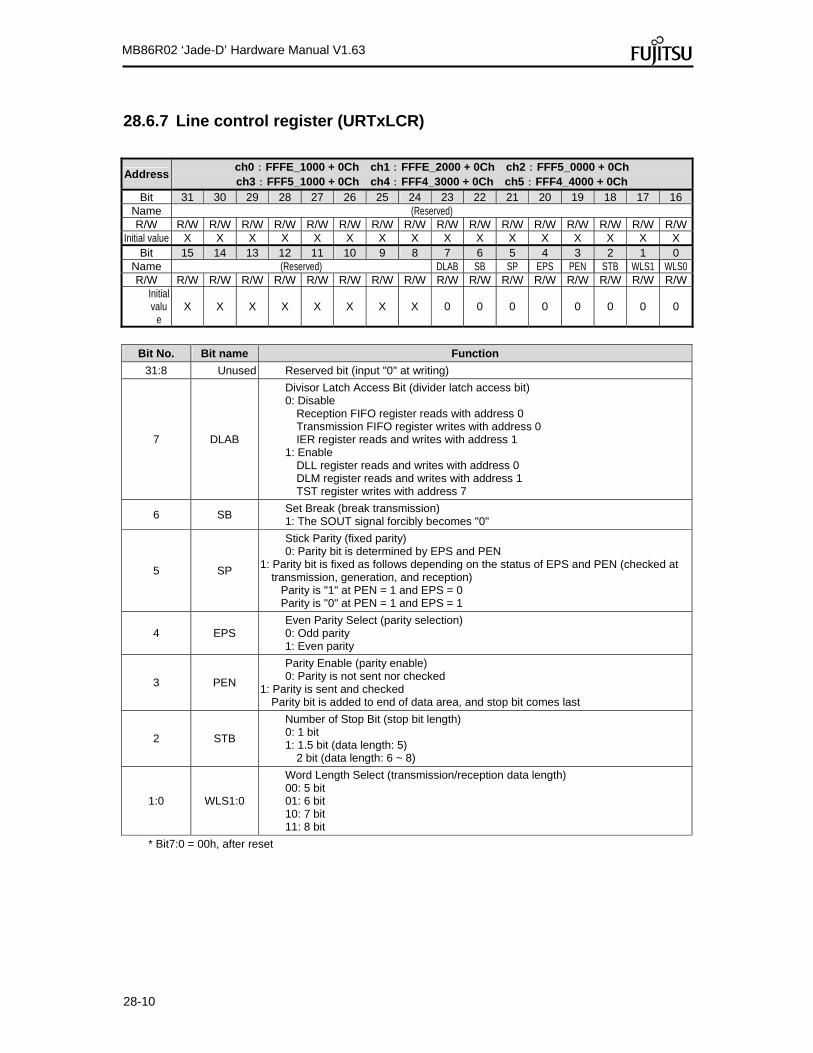
28-10
MB86R02 ‘Jade-D’ Hardware Manual V1.63
28.6.7 Line control register (URTxLCR)
Address ch0:FFFE_1000 + 0Ch ch1:FFFE_2000 + 0Ch ch2:FFF5_0000 + 0Ch ch3:FFF5_1000 + 0Ch ch4:FFF4_3000 + 0Ch ch5:FFF4_4000 + 0Ch
Bit 31 30 29 28 27 26 25 24 23 22 21 20 19 18 17 16 Name (Reserved) R/W R/W R/W R/W R/W R/W R/W R/W R/W R/W R/W R/W R/W R/W R/W R/W R/W
Initial value X X X X X X X X X X X X X X X X Bit 15 14 13 12 11 10 9 8 7 6 5 4 3 2 1 0
Name (Reserved) DLAB SB SP EPS PEN STB WLS1 WLS0R/W R/W R/W R/W R/W R/W R/W R/W R/W R/W R/W R/W R/W R/W R/W R/W R/W
Initial valu
e X X X X X X X X 0 0 0 0 0 0 0 0
Bit No. Bit name Function
31:8 Unused Reserved bit (input "0" at writing)
7 DLAB
Divisor Latch Access Bit (divider latch access bit) 0: Disable
Reception FIFO register reads with address 0 Transmission FIFO register writes with address 0 IER register reads and writes with address 1
1: Enable DLL register reads and writes with address 0 DLM register reads and writes with address 1 TST register writes with address 7
6 SB Set Break (break transmission) 1: The SOUT signal forcibly becomes "0"
5 SP
Stick Parity (fixed parity) 0: Parity bit is determined by EPS and PEN
1: Parity bit is fixed as follows depending on the status of EPS and PEN (checked at transmission, generation, and reception)
Parity is "1" at PEN = 1 and EPS = 0 Parity is "0" at PEN = 1 and EPS = 1
4 EPS Even Parity Select (parity selection) 0: Odd parity 1: Even parity
3 PEN
Parity Enable (parity enable) 0: Parity is not sent nor checked
1: Parity is sent and checked Parity bit is added to end of data area, and stop bit comes last
2 STB
Number of Stop Bit (stop bit length) 0: 1 bit 1: 1.5 bit (data length: 5)
2 bit (data length: 6 ~ 8)
1:0 WLS1:0
Word Length Select (transmission/reception data length) 00: 5 bit 01: 6 bit 10: 7 bit 11: 8 bit
* Bit7:0 = 00h, after reset
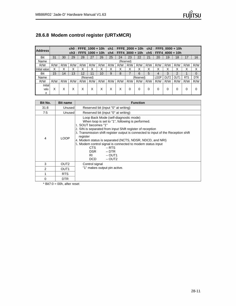
28-11
MB86R02 ‘Jade-D’ Hardware Manual V1.63
28.6.8 Modem control register (URTxMCR)
Address ch0:FFFE_1000 + 10h ch1:FFFE_2000 + 10h ch2:FFF5_0000 + 10h ch3:FFF5_1000 + 10h ch4:FFF4_3000 + 10h ch5:FFF4_4000 + 10h
Bit 31 30 29 28 27 26 25 24 23 22 21 20 19 18 17 16 Name (Reserved) R/W R/W R/W R/W R/W R/W R/W R/W R/W R/W R/W R/W R/W R/W R/W R/W R/W
Initial value X X X X X X X X X X X X X X X X Bit 15 14 13 12 11 10 9 8 7 6 5 4 3 2 1 0
Name (Reserved) (Reserved) LOOP OUT2 OUT1 RTS DTR R/W R/W R/W R/W R/W R/W R/W R/W R/W R/W R/W R/W R/W R/W R/W R/W R/W
Initial valu
e X X X X X X X X 0 0 0 0 0 0 0 0
Bit No. Bit name Function
31:8 Unused Reserved bit (input "0" at writing)
7:5 Unused Reserved bit (input "0" at writing)
4 LOOP
Loop Back Mode (self-diagnostic mode) When loop is set to "1", following is performed.
1. SOUT becomes "1" 2. SIN is separated from input Shift register of reception 3. Transmission shift register output is connected to input of the Reception shift
register 4. Modem status is separated (NCTS, NDSR, NDCD, and NRI) 5. Modem control signal is connected to modem status input
CTS – RTS DSR – DTR RI – OUT1 DCD – OUT2
3 OUT2 Control signal "1" makes output pin active. 2 OUT1
1 RTS
0 DTR
* Bit7:0 = 00h, after reset

28-12
MB86R02 ‘Jade-D’ Hardware Manual V1.63
28.6.9 Line status register (URTxLSR)
Address ch0:FFFE_1000 + 14h ch1:FFFE_2000 + 14h ch2:FFF5_0000 + 14h ch3:FFF5_1000 + 14h ch4:FFF4_3000 + 14h ch5:FFF4_4000 + 14h
Bit 31 30 29 28 27 26 25 24 23 22 21 20 19 18 17 16 Name (Reserved) R/W R R R R R R R R R R R R R R R R
Initial value X X X X X X X X X X X X X X X X Bit 15 14 13 12 11 10 9 8 7 6 5 4 3 2 1 0
Name (Reserved) ERRF TEMT THRE BI FE PE OE DR R/W R R R R R R R R R R R R R R R R
Initial valu
e X X X X X X X X 0 1 1 0 0 0 0 0
Bit No. Bit name Function
31:8 Unused Reserved bit
7 ERRF
Error in RCVR FIFO (error in reception FIFO) This bit is set even 1 error of parity, flaming, or break detection is in reception FIFO. If data including error (except the one set ERRF flag) is not in reception FIFO at reading LSR register, this is reset.
6 TEMT Transmitter Empty (transmission shift register empty) When both Transmission shift register and Transmission FIFO register become empty, TEMT is set to "1".
5 THRE
Transmitter FIFO Register Empty (transmission register empty) When Transmission FIFO register is empty and ready to accept new data, THRE is set to "1". This bit is cleared at sending data to Transmission shift register.
4 BI Break Interrupt (break reception) This bit is set when SIN is held in "0" more than transmission time (start bit + databit + parity + stop bit.) BI is reset by CPU reading this register.
3 FE Framing Error (flaming error) This bit is set when reception data does not have valid stop bit. FE is reset by CPU reading this register.
2 PE Parity Error (parity error) This bit is set when reception data does not have valid parity bit. PE is reset by CPU reading this register.
1 OE Overrun Error (overrunning error) This bit is set when reception FIFO is full and receives the next reception data. OE is reset by CPU reading this register.
0 DR Data Ready (reception data existed) This bit shows 1 byte or more of data is in FIFO. This bit is set when data is in FIFO and reset after reading all data in FIFO.
* Bit7:0 = 60h, after reset

28-13
MB86R02 ‘Jade-D’ Hardware Manual V1.63
28.6.10 Modem status register (URTxMSR)
Address ch0:FFFE_1000 + 18h ch1:FFFE_2000 + 18h ch2:FFF5_0000 + 18h ch3:FFF5_1000 + 18h ch4:FFF4_3000 + 18h ch5:FFF4_4000 + 18h
Bit 31 30 29 28 27 26 25 24 23 22 21 20 19 18 17 16 Name (Reserved) R/W R R R R R R R R R R R R R R R R
Initial value X X X X X X X X X X X X X X X X Bit 15 14 13 12 11 10 9 8 7 6 5 4 3 2 1 0
Name (Reserved) DCD RI DSR CTS DDCD TERI DDSR DCTSR/W R R R R R R R R R R R R R R R R
Initial valu
e X X X X X X X X X X X X 0 0 0 0
Bit No. Bit name Function
31:8 Unused Reserved bit
7 DCD Data Carrier Detect Loop = 0: Inversed input signal, XDCD is indicated Loop = 1: It is equal to OUT2 of MCR
6 RI Ring Indicator Loop = 0: Inversed input signal, XRI is indicated Loop = 1: It is equal to OUT1 of MCR
5 DSR Data Set Ready Loop = 0: Inversed input signal, XDSR is indicated Loop = 1: It is equal to DTR of MCR
4 CTS Clear To Send Loop = 0: Inversed input signal, XCTS is indicated Loop = 1: It is equal to RTS of MCR
3 DDCD Delta Data Carrier Detect This bit is set when DCD signal changes after the last reading by CPU. The bit is reset by reading this register.
2 TERI Traling Edge of Ring Indicator This bit is set when RI signal changes from 1 to 0 after the last reading by CPU. The bit is reset by reading this register.
1 DDSR Delta Data Set Ready This bit is set when DSR signal changes after the last reading by CPU. The bit isreset by reading this register.
0 DCTS Delta Clear To Send This bit is set when CTS signal changes after the last reading by CPU. The bit isreset by reading this register.
* Bit7:0 = x0h, after reset Bit7:4 is monitor bit of external pin

28-14
MB86R02 ‘Jade-D’ Hardware Manual V1.63
28.6.11 Divider latch register (URTxDLL&URTxDLM)
This register is frequency dividing latch to generate necessary baud rate from clock input. Frequency diving latch consists of 16 bit, DLM (high order byte) and DLL (low order byte.)
[DLL]
Address ch0:FFFE_1000 + 00h ch1:FFFE_2000 + 00h ch2:FFF5_0000 + 00h ch3:FFF5_1000 + 00h ch4:FFF4_3000 + 00h ch5:FFF4_4000 + 00h
(Accessing is enabled only at DLAB = 1) Bit 31 30 29 28 27 26 25 24 23 22 21 20 19 18 17 16
Name (Reserved) R/W R/W R/W R/W R/W R/W R/W R/W R/W R/W R/W R/W R/W R/W R/W R/W R/W
Initial value X X X X X X X X X X X X X X X X Bit 15 14 13 12 11 10 9 8 7 6 5 4 3 2 1 0
Name (Reserved) DL[7:0] R/W R/W R/W R/W R/W R/W R/W R/W R/W R/W R/W R/W R/W R/W R/W R/W R/W
Initial valu
e X X X X X X X X 0 0 0 0 0 0 0 0
[DLM]
Address ch0:FFFE_1000 + 04h ch1:FFFE_2000 + 04h ch2:FFF5_0000 + 04h ch3:FFF5_1000 + 04h ch4:FFF4_3000 + 04h ch5:FFF4_4000 + 04h
(Accessing is enabled only at DLAB = 1)) Bit 31 30 29 28 27 26 25 24 23 22 21 20 19 18 17 16
Name (Reserved) R/W R/W R/W R/W R/W R/W R/W R/W R/W R/W R/W R/W R/W R/W R/W R/W R/W
Initial value X X X X X X X X X X X X X X X X Bit 15 14 13 12 11 10 9 8 7 6 5 4 3 2 1 0
Name (Reserved) DL[15:0] R/W R/W R/W R/W R/W R/W R/W R/W R/W R/W R/W R/W R/W R/W R/W R/W R/W
Initial valu
e X X X X X X X X 0 0 0 0 0 0 0 0
DLL and DLM are read/written when DLAB bit of LCR is set to "1". After the reset, DLL and DLM are 00h DLL and DLM values are loaded by writing to either DLL or DLM Baud rate is settable in the range that DLM and DLL are FFFFh ~ 0001h

28-15
MB86R02 ‘Jade-D’ Hardware Manual V1.63
To calculate transfer baud rate
Transfer baud rate (bps) = (APB clock frequency (Hz)/Frequency dividing value)/16
Example of frequency dividing value (DLM and DLL values) and baud rate is shown in Table 28-2.
Table 28-2 Example of frequency dividing value (DLM and DLL values) and baud rate
DLL value (decimal) (DLM = 0)
MB86R02 'JADE-D' baud rateThe other party's baud rate
(error range) APB clock = 41.663(MHz)
(external input condition: CLK = 25.0MHz, CRIPM[3:0] = 0001)
2170 1200 1200 (100%)
1085 2400 2400 (100%)
542 4804 4800 (99.9%)
271 9609 9600 (99.9%)
181 14386 14400 (100.1%)
136 19147 19200 (100.3%)
90 28933 28800 (99.5%)
68 38293 38400 (100.3%)
45 57865 57600 (99.5%)
23 113215 115200 (101.8%)
Transmission baud rate on the other party and baud rate used by macro are able to receive data properly within the permissible error range. Out of the range causes reception error. Baud rate's permissible error range that macro permits is shown below.
104.1% > Macro baud rate (100%) > 95.3%
When baud rate used by macro is within the reception baud rate's permissible error range of the other party, data is able to be received. Out of the range causes error on the other party side. After the reset (MR = 1), it takes 1/4 bit of time from setting DLL and DLM to enable start bit detection. Although start bit (SIN = 0) is received in the period, proper start bit detection is not performed.
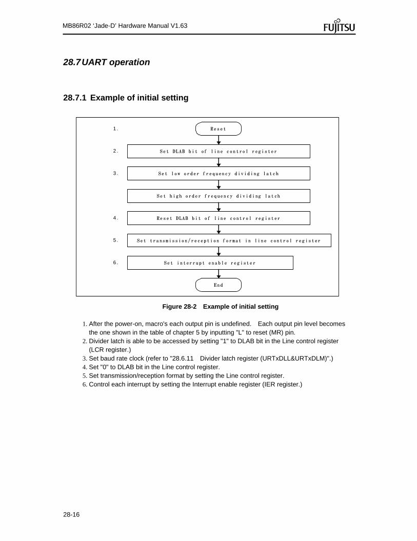
28-16
MB86R02 ‘Jade-D’ Hardware Manual V1.63
28.7 UART operation
28.7.1 Example of initial setting
1 .
2 .
3 .
4 .
5 .
6 .
Figure 28-2 Example of initial setting
1. After the power-on, macro's each output pin is undefined. Each output pin level becomes the one shown in the table of chapter 5 by inputting "L" to reset (MR) pin.
2. Divider latch is able to be accessed by setting "1" to DLAB bit in the Line control register (LCR register.)
3. Set baud rate clock (refer to "28.6.11 Divider latch register (URTxDLL&URTxDLM)".) 4. Set "0" to DLAB bit in the Line control register. 5. Set transmission/reception format by setting the Line control register. 6. Control each interrupt by setting the Interrupt enable register (IER register.)

28-17
MB86R02 ‘Jade-D’ Hardware Manual V1.63
28.7.2 Example of transfer procedure
N o
1 .
2 .
Yes
Figure 28-3 Example of transfer procedure 1. Check transmission FIFO is empty with following method:
a. Polling process of THRE bit in the Line status register (LSR) THRE bit shows transmission FIFO status. When the FIFO is empty, the bit becomes "1".
b. Polling process of TEMT bit in the Line status register (LSR) TEMT bit shows transmission FIFO and Transmission shift register statuses that data in transmission process and empty transmission FIFO are able to be confirmed. When they are empty, TEMT becomes "1".
c. Transmission FIFO empty interrupt process When all data in transmission FIFO is moved to the Transmission shift register, this interrupt occurs. It is able to control approval/prohibition in the Interrupt enable register (URTxIER.)
Note: During transmission FIFO empty interrupt process, check THRE bit of the LSR is "1" before writing data to transmission FIFO.
THRE = 1: Transmission FIFO is empty that data is able to be written THRE = 0: Transmission FIFO is not empty. Retry from interrupt process to be
FIFO empty interrupt status without writing data to transmission FIFO.
2. Set transmission data to transmission FIFO. Up to 16 byte is able to be set in the FIFO at a time. In this case, THRE bit of the LSR becomes "0".
Note:
The last written data is deleted when writing data to transmission FIFO while it is full.

28-18
MB86R02 ‘Jade-D’ Hardware Manual V1.63
28.7.3 Example of reception procedure
1 .
2 .
3 . 4 .
Figure 28-4 Example of reception procedure
1. When certain interrupt is permitted, interrupt occurrence is able to be confirmed with interrupt (INTR) pin (at INTR = "H".) Moreover, it is confirmed by polling NINT bit in the Interrupt ID register (IIR register) (at NINT = "0".)
2. Type of interrupt is able to be observed by confirming ID0, ID1 and ID2 bit in the Interrupt ID register.
3. After interrupt type is judged as reception line status interrupt with the process in item 2, reception error information is able to be acquired by reading the Line status register which also releases the interrupt (INTR= "L".)
4. After interrupt type is judged as reception data ready interrupt with the process in item 2, read number of character corresponding to the trigger level to acquire reception character. Reception data ready status is also able to be confirmed by referring DR bit in the Line status register. The interrupt is released when data in FIFO becomes less than the trigger level (INTR= "L".)

28-19
MB86R02 ‘Jade-D’ Hardware Manual V1.63
28.7.4 Basic transmission operation
Figure 28-5 Basic transmission operation When initial reset is completed and transmission data is not written to the Transmission shift register in the transmission control part (mark state), state of "H" level continues applying to serial transmission (SOUT) pin. The data is output from serial transmission (SOUT) pin with adding start bit, parity bit, and stop bit in the transmission control part as shown in Figure 28-5 when transmission data is written from CPU to transmission FIFO. 1 ~ 16 byte of transmission data is able to be consecutively written to transmission FIFO at a time. Transmission FIFO state is able to be confirmed with THRE bit of the LSR register. When transmission data is written to transmission FIFO though it is full, the last written data is deleted. The data that is already stored in the transmission FIFO is properly transmitted. THRE bit becomes "0" by writing to transmission FIFO. When the writing data is transferred to the Transmission shift register and FIFO becomes empty, the value becomes "1". If transmission data buffer interrupt is permitted in that time, interrupt (INTR) pin becomes "H" and interrupt occurs. This interrupt is released by writing data to the transmission FIFO again or reading the Interrupt confirmation register. TEMT bit becomes "0" at the same timing of THRE bit, and the value becomes "1" after transmission of all written data is completed. XTXRDY is data ready signal that shows possible transmission to DMA controller at using the controller. Single transfer mode is supported when bit 3 of the FCR register is "0" and the demand transfer mode is supported when the bit is "1". When transmission baud rate used by macro is within the reception baud rate permissible error range, the other party is able to receive data. Out of the range causes reception error on the other party side.

28-20
MB86R02 ‘Jade-D’ Hardware Manual V1.63
28.7.5 Basic reception operation
Figure 28-6 Basic reception operation After detecting received start bit ("L" level) from serial input (SIN) pin, the bit receiving next is regarded as start bit of reception data. Then, received data is sampled with reception clock, and stop bit is detected after receiving data bit and parity bit. When transmission error occurs during that time, its factor (break detection, flaming error, parity error, and overrunning error) is applied to each data in FIFO, and the status is maintained. Status can be confirmed by CPU at the first data of FIFO. When reception data ready interrupt is permitted, interrupt (INTR) pin becomes "H" and interrupt occurs by reaching the data in reception FIFO to the trigger level. This interrupt is released when the data in the FIFO becomes less than the trigger level, and interrupt (INTR) pin becomes "L". XRXRDY is data ready signal that shows possible reception to DMA controller at using the controller. Single transfer mode is supported when bit 3 of the FCR register is "0" and the demand transfer mode is supported when the bit is "1". When transmission baud rate of the other party and baud rate used by macro are within the reception baud rate permissible error range, data is able to be received properly. Out of the range causes reception error. Baud rate permissible error range that macro permits is as follows.
104.1% > Macro baud rate (100%) > 95.3%
After reset (MR = 1), the time reaching to enable detection of start bit is 1/4 bit after DLL and DLM are set. Even if start bit (SIN=0) is received during this period, normal start bit detection is not performed.

28-21
MB86R02 ‘Jade-D’ Hardware Manual V1.63
28.7.6 Line status
THRE flag and TEMT flag Operation example of THRE flag and TEMT flag of bit 5 and 6 in the Line status register (LSR) is shown in Figure 28-7.
Figure 28-7 Example of operation of THRE flag and TEMT flag THRE flag = "1" indicates that there is no data in the Transmission FIFO buffer register, and transmission character is able to be written. TEMT flag becomes "1" when there is no data in the register and Transmission shift register in the transmission control part. Both flags become "0" at writing "0" to transmission FIFO buffer.

28-22
MB86R02 ‘Jade-D’ Hardware Manual V1.63
FE flag and BI flag Operation example of BI flag and of bit 4 and 3 and FE flag in the Line status register (LSR) is shown in Figure 28-8.
Figure 28-8 Operation example of FE flag and BI flag
If "L" level is received at the stop bit during reception operation, flaming error occurs and FE flag becomes "1". The error flag is reset by reading Line status register. When "L" level continues during transmission time (start bit, data bit, parity bit, and stop bit) for 1 character, break code is detected. These errors are applied to each data in FIFO, and they are able to be confirmed when CPU reads the first data of FIFO. FE and BI flags are able to be confirmed in the Status register at reading Line status register whose first data includes framing and break detection error. Both flags become "0" by reading Status register. For the case of break detection error, reception data is stored to FIFO as 0. When break is detected, macro stops reception, and it restarts the process with detecting SIN's falling edge.

28-23
MB86R02 ‘Jade-D’ Hardware Manual V1.63
PE flag Operation example of PE flag of bit 2 in the Line status register (LSR) is shown in Figure 28-9.
Figure 28-9 Operation example of PE flag (setting even parity) Parity bit is set to "1" or "0" depending on the number of "1" level bit in the 1 data bit. When it is set to even parity with EPS in the Line control register, the bit is set to "1" or "0" to have total data bit and "1" level parity bit even number. Likewise, when parity bit is set to odd parity, total number of "1" level is set to be odd number. On reception side, the number of "1" level bit of 1 data including input parity bit is counted, and polarity of the parity set with EPS bit in the Line control register is compared. For their discrepancy, PE flag of the register becomes "1" by the judgment that problem occurred in transmitting data. Then the flag becomes "0" by reading the Line status register. This error is applied to each data in FIFO, and is able to be confirmed when CPU reads first data of FIFO.

28-24
MB86R02 ‘Jade-D’ Hardware Manual V1.63
OE flag Operation example of OE flag of bit 1 in the Line status register (LSR) is shown in Figure 28-10.
Figure 28-10 Operation example of OE flag When next character is received completely to the Reception shift register in the status that reception FIFO is full, overrun error occurs. In this case, OE flag of the Line status register is set immediately and interrupt occurs (if it is permitted.)
DR flag Operation example of DR flag of bit 0 in the Line status register (LSR) is shown in Figure 28-11.
Figure 28-11 Operation example of DR flag When reception data is received and 1 byte or more of data is stored in reception FIFO, DR flag of the Line status register becomes "1". The flag becomes "0" by reading reception FIFO data and FIFO becomes empty.
ERRF flag When error (parity, break detection, and flaming) is included in the data stored in reception FIFO, ERRF flag of bit 7 of the Line status register (LSR) is set to "1" during reception operation. If there is no error data in FIFO except the one set ERRF flag when CPU reads the register, this flag is cleared to "0".

28-25
MB86R02 ‘Jade-D’ Hardware Manual V1.63
28.7.7 Character time-out interrupt
Character time-out interrupt occurs in the following cases: 1 or more data is stored in reception FIFO and the next serial data is still not received after 4
characters of time 1 or more data is stored in reception FIFO and CPU still does not read the data after 4
characters of time When time-out interrupt occurs, INTR pin becomes "H". Moreover, XRXRDY signal becomes "L", showing DMA controller that reception is ready, and requests to read data. Timer and time-out interrupt are reset by CPU (or DMA controller) reading 1 byte from reception FIFO. If time-out does not occur, it is reset after timer receives new data or CPU (or DMA controller) reads data from reception FIFO.

29-1
MB86R02 ‘Jade-D’ Hardware Manual V1.63
29 I2C Bus Interface This chapter describes the functionality and operation of the I2C bus interface.
29.1 Outline
The I2C bus is a serial bus advocated by Philips Semiconductors (now NXP) that supports data exchange between multiple devices using 2 signal lines. The MB86R02 has 2 interface channels that support the I2C standard mode (max. 100Kbps)/high-speed mode (max. 400KBps). The xxternal pins I2C_SDA0, I2C_SDA1, I2C_SCL0 and I2C_SCL1 exclusively use 3.3V, so that the device can be used for 3.3V I2C communication. I2C_SDA0/I2C_SDA1 are referred to as the SDA line and I2C_SCL0/I2C_SCL1 are referred to as the SCL line in this document.
29.2 Features
The I2C modules have the following features: Master transmission/reception function Slave transmission/reception function Arbitration function Clock synchronization function Slave address detecting function General call address detecting function Transfer direction detecting function Repeat occurrence and detecting function of start condition Bus error detecting function Corresponding to standard mode (max. 100KBps)/high-speed mode (max. 400KBps)

29-2
MB86R02 ‘Jade-D’ Hardware Manual V1.63
29.3 Block diagram
Figure 29-1 shows a block diagram of the I2C modules.
Start condition/Stop condition
detector
Arbitration lost
detector
Start condition/Stop condition
detector
Shift Clock
generator
I2C_SDA0
I2C_SCL0 Noise
filter
I2CADR
APB bus
I2C module 0
I2C module 1
I2C_SDA1
I2C_SCL1
MB86R01
Comparator
I2CDAR
I2CBSR
I2CBCR
I2CCCR
I2CBC2R
I2CECSR
I2CBCFR
Figure 29-1 Block diagram of the I2C modules
29-3
MB86R02 ‘Jade-D’ Hardware Manual V1.63
29.4 Block functions
The function of each block is described below.
Block Description
Start condition/Stop condition detector
Start condition and Stop condition are detected by the transition state of the SDA and SCL lines.
Start condition/Stop condition generator
The Start condition and Stop condition are generated by the transition state of the SDA and SCL lines.
Arbitration lost detector Output data to SDA line and input data from SDA line are compared at data transmission. If they do not match, arbitration is lost.
Shift clock generator Timing count of serial data t transfer clock occurrence and output control of SCL line clock are performed via the clock control register setting.
Comparator Compares the received address and self-address specified in the address register or received address and global address.
I2CxADR 7 bit register that specifies the slave address.
I2CxDAR 8 bit register used for serial data transfer.
I2CxBSR 8 bit register with following functions to show I2C bus status and others. Repeated start condition detection Arbitration lost detection Acknowledge bit storage Direction of data transfer Addressing detection General call address detection First byte detection
I2CxBCR 8 bit register that performs I2C bus control and interrupt control has following functions. Interrupt request/permission Start condition occurrence Master/Slave selection Acknowledge occurrence permission
I2CxCCR 7 bit register that sets clock frequency of serial data transfer. Operation permission Frequency setting of serial clock Standard/High-speed mode selection
Noise filter This noise filter is composed of a 3-stage shift register circuit. If all 3 values consecutively sampled on the SCL/SDA lines are "1", the filter output is a "1". If the values are all "0", the filter output is "0". For other sampled values, the previous state 1 clock is maintained.
I2CxBC2R This is the register to drive "L" forcibly and to confirm the line status after the noise filter.
I2CxECSR This is the register to enhance CS bit in I2CxCCR register.
I2CxBCFR This is the register that specifies the frequency range of the bus clock to be used.

29-4
MB86R02 ‘Jade-D’ Hardware Manual V1.63
29.5 Related pins
I2C uses the following pins.
Pin Direction Qty. Description
I2C_SCL0 I2C_SCL1
IN/OUT 2
Clock pin of the I2C bus interface. The last number of the pin name indicates the I2C channel number. The output of this pin is open drain.
I2C_SDA0 I2C_SDA1
IN/OUT 2
Data pin of the I2C bus interface. The last number of the pin name indicates the I2C channel number. The output of this pin is open drain.
29.6 Supply clock
The APB clock is supplied to the I2C modules. Refer to "5. Clock reset generator (CRG)" for frequency setting and control specification of the clock.

29-5
MB86R02 ‘Jade-D’ Hardware Manual V1.63
29.7 Register
This section describes the I2C bus interface register.
29.7.1 Register list
The MB86R02 'Jade-D' device has 2 I2C bus interface channels and each module has the registers shown in Table 29-1.
Table 29-1 I2C register list
Channel Address Register Description
I2C ch0 FFF56000h I2C0BSR Bus status register
FFF56004h I2C0BCR Bus control register
FFF56008h I2C0CCR Clock control register
FFF5600Ch I2C0ADR Address register
FFF56010h I2C0DAR Data register
FFF56014h I2C0ECSR Extension CS register
FFF56018h I2C0BCFR Bus clock frequency register
FFF5601Ch I2C0BC2R Bus control 2 register
I2C ch1 FFF57000h I2C1BSR Bus status register
FFF57004h I2C1BCR Bus control register
FFF57008h I2C1CCR Clock control register
FFF5700Ch I2C1ADR Address register
FFF57010h I2C1DAR Data register
FFF57014h I2C1ECSR Extension CS register
FFF57018h I2C1BCFR Bus clock frequency register
FFF5701Ch I2C1BC2R Bus control 2 register
Note:
Access the area of I2C ch0 and I2C ch1 in 32 bit (word).

29-6
MB86R02 ‘Jade-D’ Hardware Manual V1.63
Description format of register Following format is used for description of register’s each bit in "29.7.2 Bus status register (I2CxBSR)" to "29.7.9 Bus clock frequency register (I2CxBCFR)". Address Base address + Offset
Bit 31 30 29 28 27 26 25 24 23 22 21 20 19 18 17 16 Name R/W
Initial value Bit 15 14 13 12 11 10 9 8 7 6 5 4 3 2 1 0
Name R/W
Initial valu
e
Meaning of item and sign Address
Address (base address + offset address) of the register Bit
Bit number of the register Name
Bit field name of the register R/W
Attribution of read/write of each bit field R0:Read value is always "0" R1: Read value is always "1" W0: Write value is always "0", and write access of "1" is ignored W1: Write value is always "1", and write access of "0" is ignored R: Read W: Write Initial value
Each bit field’s value after reset 0: Value is "0" 1: Value is "1" X: Value is undefined

29-7
MB86R02 ‘Jade-D’ Hardware Manual V1.63
29.7.2 Bus status register (I2CxBSR)
Address ch0:FFF5_6000 + 00h ch1:FFF5_7000 + 00h
Bit 31 30 29 28 27 26 25 24 23 22 21 20 19 18 17 16 Name (Reserved) R/W R R R R R R R R R R R R R R R R
Initial value 0 0 0 0 0 0 0 0 0 0 0 0 0 0 0 0 Bit 15 14 13 12 11 10 9 8 7 6 5 4 3 2 1 0
Name (Reserved) BB RSC AL LRB TRX AAS GCA FBT R/W R R R R R R R R R R R R R R R R
Initial valu
e 0 0 0 0 0 0 0 0 0 0 0 0 0 0 0 0
All bits of this register are cleared when the EN bit of I2CxCCR is "0".
Bit 7: BB (bus busy) This bit shows I2C bus state.
BB Status
0 Stop condition is detected
1 Start condition is detected (but is in use)
Bit 6: RSC (Repeated Start Condition) Repeated start condition detecting bit.
RSC State
0 Repeated start condition is not detected
1 Start condition is detected again during bus is in use
This bit is cleared by writing "0" to the INT bit. Start condition detection at bus stop and stop condition detection as well as addressing are not performed by the slave. Bit 5: AL (Arbitration Lost) Arbitration lost detection bit
AL State
0 Arbitration lost is not detected
1 Arbitration lost occurs during master transmission, or "1" is written to MSS bit while other systems are using bus
This bit is cleared by writing "0" to the INT bit.
Restrictions:
In a multimaster environment, please prohibit other masters from transmitting general call addresses simultaneously with this module, as well as using 'arbitration lost' for this module at the second byte or later.

29-8
MB86R02 ‘Jade-D’ Hardware Manual V1.63
Bit 4: LRB (LAST Received Bit) This bit is to store the 9th bit of the data indicating acknowledge (ACK)/negative acknowledge (NACK).
LRB State
0 Acknowledge (ACK) is detected
1 Negative acknowledge (NACK) is detected
This bit is cleared on start condition detection or stop condition detection. Bit 3: TRX (Transfer/Receive) This bit is to indicate transmission/reception state of data transfer.
TRX State
0 Reception state
1 Transmission state
Bit 2: AAS (Address As Slave) This is the addressing detection bit.
AAS State
0 Addressing is not performed by slave
1 Addressing is performed by slave
This is cleared on start condition detection or stop condition detection. Bit 1: GCA (General Call Address) This is general call address (00h) detecting bit.
GCA State
0 General call address is not received at slave
1 General call address is received at slave
This bit is cleared on start condition detection or stop condition detection. Bit 0: FBT (First Byte Transfer) This is the first byte detection bit.
FBT State
0 Reception data is not first byte
1 Reception data is the first byte (address data)
Although this is set to "1" on start condition detection, it is cleared if "0" is written to the INT bit and addressing is not performed by the slave.

29-9
MB86R02 ‘Jade-D’ Hardware Manual V1.63
29.7.3 Bus control register (I2CxBCR)
Address ch0:FFF5_6000 + 04h ch1:FFF5_7000 + 04h
Bit 31 30 29 28 27 26 25 24 23 22 21 20 19 18 17 16 Name (Reserved) R/W R R R R R R R R R R R R R R R R
Initial value 0 0 0 0 0 0 0 0 0 0 0 0 0 0 0 0 Bit 15 14 13 12 11 10 9 8 7 6 5 4 3 2 1 0
Name (Reserved) BER BEIE SCC MSS ACK GCAA INTE INT R/W R R R R R R R R R/W R/W R/W R/W R/W R/W R/W R/W
Initial valu
e 0 0 0 0 0 0 0 0 0 0 0 0 0 0 0 0
This is cleared (except bits 7 and 6) when the EN bit of I2CxCCR is "0".
Bit 7: BER (Bus ERror) This is the bus error interrupt request flag bit.
For writes
BER State
0 Bus error interrupt request flag is cleared
1 N/A
For reads
BER State
0 Bus error is not detected
1 Incorrect start and stop conditions are detected during data transfer
When this bit is set, the EN bit of the I2CxCCR register is cleared, this module enters the halt state, and the data transfer is discontinued. Bit 6: BEIE (Bus Error Interrupt Enable) This is the bus error interrupt permission bit. On read/writes
BEIE State
0 Bus error interrupt is prohibited
1 Bus error interrupt is permitted
If this bit is "1" and BER bit is "1", an interrupt occurs. Bit 5: SCC (Start Condition Continue) This is the start condition generation bit. At writing
SCC State
0 N/A
1 Start condition is generated again on master transfer
This bit is automatically cleared after setting "1".

29-10
MB86R02 ‘Jade-D’ Hardware Manual V1.63
Bit 4: MSS (Master Slave Select) This is the master/slave selection bit. At writing
MSS State
0 Stop condition is generated and state becomes slave mode after the transfer
1 State becomes master mode and start condition is generated to start transfer
This bit is cleared when 'arbitration lost' occurs during master transmission and the state becomes slave mode.
Restrictions: In a multimaster environment, please prohibit other masters from transmitting general call addresses simultaneously with this module, as well as using 'arbitration lost' for this module at the second byte or later.
Bit 3: ACK (ACKnowledge) This is the acknowledge permission bit at receiving data. On reads/writes
ACK State
0 Acknowledge has not occurred.
1 Acknowledge has occurred.
This bit is disabled on address data reception in slave mode. Bit 2: GCAA (General Call Address Acknowledge) This is the acknowledge permission bit on receiving general call address. At reading/writing
GCAA State
0 Acknowledge has not occurred.
1 Acknowledge has occurred.
Bit 1: INTE (INTerrupt Enable) This is the interrupt permission bit. At reading/writing
INTE State
0 Interrupt is prohibited
1 Interrupt is enabled
When this bit is "1" and INT bit is "1" an interrupt occurs.

29-11
MB86R02 ‘Jade-D’ Hardware Manual V1.63
Bit 0: INT (INTerrupt) This is the transfer end interrupt request flag bit. On writes
INT State
0 Transfer end interrupt flag is cleared
1 N/A
On reads
INT State
0 Transfer has not completed
1
This is set when following conditions are applied on the completion of a 1 byte transfer which includes the acknowledge bit. Bus master Addressed slave General call address is received (only at GCAA = "1")
Arbitration lost occured (only at bus acquisition state) Start condition attempted while other systems are using the bus
When this bit is "1", the SCL line is held at the "L" level. This is cleared by writing "0" to this bit, then the SCL line opens and the next byte is transferred. In addition, this is cleared to "0" by an occurrence of a start condition or a stop condition in master mode. Competition of SCC, MSS, and INT bits Competition of the next byte transfer, start condition, and stop condition occurs by writing to the SCC, MSS, and INT bits simultaneously. The priority order in this case is as follows:
1. Occurrence of the next byte transfer and stop condition
When writing "0" to the INT bit and the MSS bit simultaneously, the MSS bit is prioritized and a stop condition occurs.
2. Occurrence of the next byte transfer and start condition When writing "0" to the INT bit and "1" to the SCC bit simultaneously, the SCC bit is prioritized and a start condition occurs.
3. Occurrence of start condition and stop condition Writing "1" to the SCC bit and "0" to the MSS bit simultaneously is prohibited.

29-12
MB86R02 ‘Jade-D’ Hardware Manual V1.63
29.7.4 Clock control register (I2CxCCR)
Address ch0:FFF5_6000 + 08h ch1:FFF5_7000 + 08h
Bit 31 30 29 28 27 26 25 24 23 22 21 20 19 18 17 16 Name (Reserved) R/W R R R R R R R R R R R R R R R R
Initial value 0 0 0 0 0 0 0 0 0 0 0 0 0 0 0 0 Bit 15 14 13 12 11 10 9 8 7 6 5 4 3 2 1 0
Name (Reserved) (Reserved) HSM EN CS[4:0] R/W R R R R R R R R R R/W R/W R/W R/W R/W R/W R/W
Initial valu
e 0 0 0 0 0 0 0 0 1 0 0 X X X X X
Bit 7: Unused The value is always read as '1'. Bit 6: HSM (High Speed Mode) This is the standard/high-speed setting bit. At reading/writing
HSM State
0 Standard mode
1 High-speed mode
Bit 5: EN (ENable) This is the operation permission bit. At reading/writing
EN State
0 Operation is prohibited
1 Operation is permitted
When this bit is "0", each bit of the I2CxBSR register and the I2CxBCR register (excluding the BER and BEIE bits) is cleared. When the BER bit is set, this bit is cleared.

29-13
MB86R02 ‘Jade-D’ Hardware Manual V1.63
Bit 4-0: CS4-0 (Clock Period Select 4-0) This bit is used to set the frequency of the serial transfer clock. The upper limit of the bus clock frequency can be extended using the I2CxECSR register. Refer to "29.7.8 Expansion CS register (I2CxECSR)" for details. If the I2CxECSR register is not used (the I2CxECSR register is used in its initial state), the frequency (fscl) of the serial transfer clock is calculated using the expression shown below.
Standard mode
clockAPBm
fscl _ 2)2(
:φφ
High-speed mode
tpoindecimalafteroffRound
clockAPBm
fscl
:) int(
_ 2)5.1int(
:φφ
Be sure to set fscl so that it doesn't exceed the following values during master operation.
Standard mode: 100KHz. High-speed mode: 400KHz.
The APB clock φ of this module should be used within the range shown below. If it is less than the range, transmission at the max. transfer rate is not guaranteed. If it exceeds the range, the upper limit of the bus clock frequency can be extended by setting the I2CxECSR register.
Master operation: 14MHz ~ 18MHz. Slave operation: 14MHz ~ 18MHz. During register access operation: 14MHz ~ 41.5MHz
Note:
+2 cycle is the min. overhead for detecting the output level change of the SCL line. If the rising edge delay of the SCL line is large or the clock is expanded for the slave device, the value is larger than the value stated above.
The value of m to CS4 ~ 0 is shown in the next page

29-14
MB86R02 ‘Jade-D’ Hardware Manual V1.63
CS4 CS3 CS2 CS1 CS0 m
Standard High speed
0 0 0 0 0 65 Setting prohibited
0 0 0 0 1 66 Setting prohibited
0 0 0 1 0 67 Setting prohibited
0 0 0 1 1 68 Setting prohibited
0 0 1 0 0 69 Setting prohibited
0 0 1 0 1 70 Setting prohibited
0 0 1 1 0 71 Setting prohibited
0 0 1 1 1 72 Setting prohibited
0 1 0 0 0 73 9
0 1 0 0 1 74 10
0 1 0 1 0 75 11
0 1 0 1 1 76 12
0 1 1 0 0 77 13
0 1 1 0 1 78 14
0 1 1 1 0 79 15
0 1 1 1 1 80 16
1 0 0 0 0 81 17
1 0 0 0 1 82 18
1 0 0 1 0 83 19
1 0 0 1 1 84 20
1 0 1 0 0 85 21
1 0 1 0 1 86 22
1 0 1 1 0 87 23
1 0 1 1 1 88 24
1 1 0 0 0 89 25
1 1 0 0 1 90 26
1 1 0 1 0 91 27
1 1 0 1 1 92 28
1 1 1 0 0 93 29
1 1 1 0 1 94 30
1 1 1 1 0 95 31
1 1 1 1 1 96 32

29-15
MB86R02 ‘Jade-D’ Hardware Manual V1.63
29.7.5 Address register (I2CxADR)
Address ch0:FFF5_6000 + 0Ch ch1:FFF5_7000 + 0Ch
Bit 31 30 29 28 27 26 25 24 23 22 21 20 19 18 17 16 Name (Reserved) R/W R R R R R R R R R R R R R R R R
Initial value 0 0 0 0 0 0 0 0 0 0 0 0 0 0 0 0 Bit 15 14 13 12 11 10 9 8 7 6 5 4 3 2 1 0
Name (Reserved) (Reserved) A[6:0] R/W R R R R R R R R R R/W R/W R/W R/W R/W R/W R/W
Initial valu
e 0 0 0 0 0 0 0 0 1 X X X X X X X
Bit 7: Unused The value is always read as '1'. Bit 6-0: A6-0 (Address 6-0) This is the slave address storage bit. The comparison with the I2CxDAR register is performed after address data reception at the slave. If they are matched, an acknowledge is transmitted to the master.

29-16
MB86R02 ‘Jade-D’ Hardware Manual V1.63
29.7.6 Data register (I2CxDAR)
Address ch0:FFF5_6000 + 10h ch1:FFF5_7000 + 10h
Bit 31 30 29 28 27 26 25 24 23 22 21 20 19 18 17 16 Name (Reserved) R/W R R R R R R R R R R R R R R R R
Initial value 0 0 0 0 0 0 0 0 0 0 0 0 0 0 0 0 Bit 15 14 13 12 11 10 9 8 7 6 5 4 3 2 1 0
Name (Reserved) D[7:0] R/W R R R R R R R R R/W R/W R/W R/W R/W R/W R/W R/W
Initial valu
e 0 0 0 0 0 0 0 0 X X X X X X X X
Bit 7-0: D7-0 (Data 7-0) This is the serial data storage bit. This data register is used for serial transfer transmitted from MSB. When data is received (TRX = 0), the data output becomes "1". This register's writing side is double-buffered so that writing data is loaded to the serial transfer register on the transmission of each byte if the bus (BB = 1) is in use. As the serial transfer register is directly read on reading, the received data is only valid if the INT bit is set.
29-17
MB86R02 ‘Jade-D’ Hardware Manual V1.63
29.7.7 Two bus control registers (I2CxBC2R)
Address ch0:FFF5_6000 + 1Ch ch1:FFF5_7000 + 1Ch
Bit 31 30 29 28 27 26 25 24 23 22 21 20 19 18 17 16 Name (Reserved) R/W R R R R R R R R R R R R R R R R
Initial value 0 0 0 0 0 0 0 0 0 0 0 0 0 0 0 0 Bit 15 14 13 12 11 10 9 8 7 6 5 4 3 2 1 0
Name (Reserved) (Reserved) SDAS SCLS (Reserved) SDAL SCLL R/W R R R R R R R R R R R R R R R/W R/W
Initial valu
e 0 0 0 0 0 0 0 0 0 0 X X 0 0 0 0
Bit 7 and 6: Unused The value is always "00" on reads.
Bit 5: SDAS (SDA status) Indicates the signal level of the SDA line after passing the noise filter. Only reading is valid.
SDAS State
0 The SDA line is "0"
1 The SDA line is "1"
Bit 4: SCLS (SCL status) Indicates the signal level of the SCL line after passing the noise filter. Only reading is valid.
SCLS State
0 SCL line is "0"
1 SCL line is "1"
Bit 3 and 2: Unused The value is always "00" on reads. Bit 1: SDAL (SDA low drive) The SDAO output is forced to "L". Both reading/writing are valid.
SDAL State
0 SDAO output is in normal operation
1 SDAO output is forced to "L"
Bit 0: SCLL (SCL Low drive) The SCLO output is forced to "L". Both reading/writing are valid.
SCLL State
0 SCLO output is in normal operation
1 SCLO output is forced to "L"
29-18
MB86R02 ‘Jade-D’ Hardware Manual V1.63
29.7.8 Expansion CS register (I2CxECSR)
Address ch0:FFF5_6000 + 14h ch1:FFF5_7000 + 14h
Bit 31 30 29 28 27 26 25 24 23 22 21 20 19 18 17 16 Name (Reserved) R/W R R R R R R R R R R R R R R R R
Initial value 0 0 0 0 0 0 0 0 0 0 0 0 0 0 0 0 Bit 15 14 13 12 11 10 9 8 7 6 5 4 3 2 1 0
Name (Reserved) (Reserved) CS[10:5] R/W R R R R R R R R R R R/W R/W R/W R/W R/W R/W
Initial valu
e 0 0 0 0 0 0 0 0 0 0 0 0 0 0 0 0
Bit 5-0: CS10-5 (Clock Period Select 10-5) This is set to expand the upper limit of the bus clock frequency by extending CS4 ~ 0 in the I2CxCCR register. The initial value of CS10 ~ 5 is "000000" and setting other values enters the frequency upper limit expansion mode.
CS10~5 State
000000 No upper limit expansion of the bus clock frequency (only CS4 ~ 0 is used)
Other than 000000 Upper limit expansion of the bus clock frequency

29-19
MB86R02 ‘Jade-D’ Hardware Manual V1.63
Standard mode:
10)10(:
:
_ 2)2(
+~
φφ
CSofValuem
clockAPBm
fscl
High-speed mode:
tpoindecimalafteroffRound
m
mfscl
CSofValue
APBclock
:) int(
2)5.1int(
10)10(:
:
+~
φφ
Set fscl so that it does not exceed the following values during master operation.
Standard mode: 100kHz High-speed mode: 400kHz
Use the system clock of this module within the range shown below. If it is less than the range, transfer at the max. transfer rate is not guaranteed. If it exceeds the range, operation is not guaranteed.
Master operation: 14MHz ~ 41.5MHz Slave operation: 14MHz ~ 41.5MHz Register access operation: 14MHz ~ 41.5MHz
Note:
+2 cycle is the min. overhead for the detection of the output level change of the SCL line. If the rising edge delay of the SCL pin is large or the clock is expanded for the slave device, the value is larger than the one stated above.
If the extension CS register is used, m value becomes CS10 ~ 0 + 1.

29-20
MB86R02 ‘Jade-D’ Hardware Manual V1.63
29.7.9 Bus clock frequency register (I2CxBCFR)
Address ch0:FFF5_6000 + 18h ch1:FFF5_7000 + 18h
Bit 31 30 29 28 27 26 25 24 23 22 21 20 19 18 17 16 Name (Reserved) R/W R R R R R R R R R R R R R R R R
Initial value 0 0 0 0 0 0 0 0 0 0 0 0 0 0 0 0 Bit 15 14 13 12 11 10 9 8 7 6 5 4 3 2 1 0
Name (Reserved) (Reserved) FS[3:0] R/W R R R R R R R R R R R R R/W R/W R/W R/W
Initial valu
e 0 0 0 0 0 0 0 0 0 0 0 0 0 0 0 1
Bit 7 and 4: Unused The value is always "0000" on reads. Bit 3-0: FS3-0 (Bus Clock Frequency Select 3-0) Selects the frequency of the bus clock to be used. Characteristics such as noise filters are set using this register. A standard setting value is shown below however adjustment might be required depending on the I2C buffer characteristics and noise state on the I2C bus.
FS3 FS2 FS1 FS0 Frequency [MHz]
0 0 0 0 Setting prohibited
0 0 0 1 14 or more ~ Less than 20
0 0 1 0 20 or more ~ Less than 40
0 0 1 1 40 or more ~ Less than 60
0 1 0 0 –
0 1 0 1 –
0 1 1 0 –
0 1 1 1 –
1 0 0 0 –
1 0 0 1 –
1 0 1 0 –
1 0 1 1 –
1 1 0 0 –
1 1 0 1 –
1 1 1 0 –
1 1 1 1 –
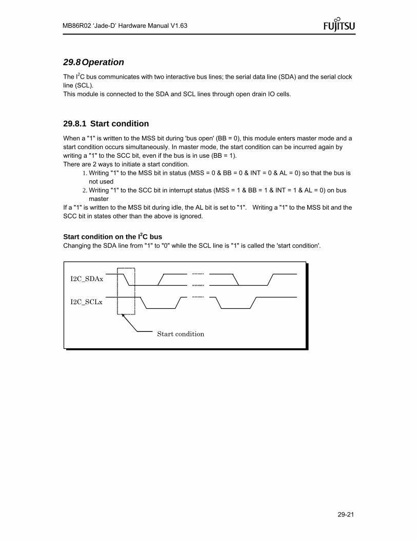
29-21
MB86R02 ‘Jade-D’ Hardware Manual V1.63
29.8 Operation
The I2C bus communicates with two interactive bus lines; the serial data line (SDA) and the serial clock line (SCL). This module is connected to the SDA and SCL lines through open drain IO cells.
29.8.1 Start condition
When a "1" is written to the MSS bit during 'bus open' (BB = 0), this module enters master mode and a start condition occurs simultaneously. In master mode, the start condition can be incurred again by writing a "1" to the SCC bit, even if the bus is in use (BB = 1). There are 2 ways to initiate a start condition.
1. Writing "1" to the MSS bit in status (MSS = 0 & BB = 0 & INT = 0 & AL = 0) so that the bus is not used
2. Writing "1" to the SCC bit in interrupt status (MSS = 1 & BB = 1 & INT = 1 & AL = 0) on bus master
If a "1" is written to the MSS bit during idle, the AL bit is set to "1". Writing a "1" to the MSS bit and the SCC bit in states other than the above is ignored.
Start condition on the I2C bus Changing the SDA line from "1" to "0" while the SCL line is "1" is called the 'start condition'.
I2C_SDAx
I2C_SCLx
Start condition

29-22
MB86R02 ‘Jade-D’ Hardware Manual V1.63
29.8.2 Stop condition
If a "0" is written to the MSS bit on master operation (MSS = 1), a stop condition occurs and the mode changes to 'slave mode'. The following show the generation of a stop condition. Writing a "0" to the MSS bit in interrupt status (MSS = 1 & BB = 1 & INT = 1 & AL = 0) on bus master. Writing a "1" to the MSS bit in states other than the above is ignored.
Stop condition on the I2C bus Changing the SDA line from "0" to "1" while the SCL line is "1" is called the 'stop condition'.
I2C_SDAx
I2C_SCLx
Stop condition

29-23
MB86R02 ‘Jade-D’ Hardware Manual V1.63
29.8.3 Addressing
In master mode, the status is set to BB = "1" and TRX = "1" after a start condition occurs and the contents of the I2CxDAR register are output starting with the MSB. When an acknowledge is received from the slave after sending the address data, bit 0 of its data (I2CxDAR register’s bit 0 after transmission) is reversed and stored in the TRX bit. In slave mode, the status is set to BB = "1" and TRX = "0" after a start condition occurs and transmission data from the master is received in the I2CxDAR register. After receiving the address data, the I2CxDAR and I2CxADR registers are compared. If they match the status is set to AAS = "1" and an acknowledge is sent to the master. Then bit 0 of the reception data (I2CxDAR register’s bit 0 after reception) is stored in the TRX bit.
Example of a slave address transmission Target slave address: 0x76 (Slave ADR register) Send: 0xEC (Master DAR register) Explanation: b1110 1100 (0xEC) is derived from b0111 0110 (0x76), left-shifted by 1 bit with a '0' added as the LSB (see also format description below).
Transfer format of slave address The transfer format of the slave address is shown below.
MSB LSB
Slave address
R/WA6 A0A5 A1 A4 A2A3 ACK
Map of slave address The slave address map is shown below.
Slave address R/W Description
0000 000 0 General call address
0000 000 1 Start byte
0000 001 X CBUS address
0000 010 X Reserved
0000 011 X Reserved
0000 1XX X
0001 XXX
1110 XXX X Available slave address
1111 0XX X 10 bit slave address (*1)
1111 1XX X Reserved
*1: This module does not support a 10 bit slave address

29-24
MB86R02 ‘Jade-D’ Hardware Manual V1.63

29-25
MB86R02 ‘Jade-D’ Hardware Manual V1.63
29.8.4 Synchronous arbitration of SCL
If multiple I2C devices try to become the master device at the same time (to operate SCL line), each device detects the SCL line status and automatically adjusts the line’s operation timing by adapting to the speed of the slowest device.
I2C_SCLx
SCL output (before arbitration)
Macro A
Macro B
Take timing from when SCL line becomes "H" to the next SCL output = "L"
Take timing from when SCL line becomes "H" to the next SCL output = "L"
SCL output (after arbitration)
SCL output (before arbitration)
SCL output (after arbitration)

29-26
MB86R02 ‘Jade-D’ Hardware Manual V1.63
29.8.5 Arbitration
Arbitration occurs when other masters attempt to transmit data at the same time. If a units own transfer data is "1" and the data on the SDA line is "0", AL = "1" is set and
arbitration is lost. If a start condition is attempted while other masters are using the bus, AL = "1" is set and
arbitration is lost. If the other masters' start condition is detected before a start condition occurs although an
unused bus is confirmed and MSS = "1" is set, then AL = "1" is set and arbitration is lost. If the AL bit is set to "1", the status becomes MSS = "0" and TRX = "0" and the state changes to slave reception mode. If arbitration is lost (the right to use the bus is lost), the master discontinues to drive the SDA line. However, driving the SCL line is not discontinued until 1 byte of the transmission ends and the interrupt is cleared.
I2C_SDAx
I2C_SCLx
SDA input
SDA output
SDA input
SDA output
Macro A
Macro B
Since input and output are matched, right to use bus is acquired.
Since input and output are unmatched, right to use bus is lost.

29-27
MB86R02 ‘Jade-D’ Hardware Manual V1.63
29.8.6 Acknowledge/Negative acknowledge
The nineth bit of data indicates an acknowledge (ACK)/negative acknowledge (NACK). A status of "0" is acknowledge and "1" is a negative acknowledge. The reception side transmits a acknowledge/negative acknowledge to the transmitter and this is stored in the LRB bit on data reception. If an acknowledge is not received from the master reception side during slave transmission (when a negative acknowledge is received), the state becomes TRX = "0" and the mode changes to slave reception mode. As a result, the master is able to generate a stop condition when the slave opens the SCL line.
I2C_SDAx
I2C_SCLx
SDA output
Macro A (transmission)
Macro B (reception) Reception side returns ACK/NACK to transmission side
Transmission side opens bus for ACK/NACK output on reception side
1 2 3 4 5 6 7 8 9
ACK
ACK
SCL output
SDA output
SCL output
Master generates clock
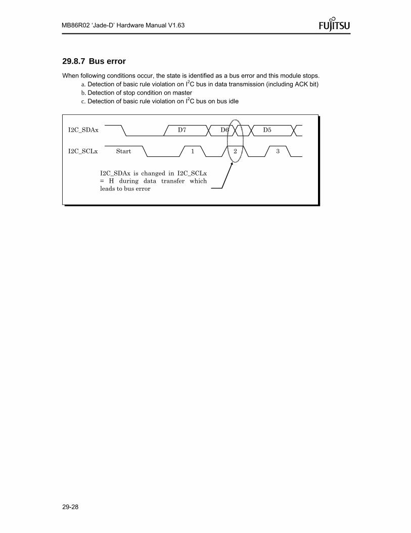
29-28
MB86R02 ‘Jade-D’ Hardware Manual V1.63
29.8.7 Bus error
When following conditions occur, the state is identified as a bus error and this module stops. a. Detection of basic rule violation on I2C bus in data transmission (including ACK bit) b. Detection of stop condition on master c. Detection of basic rule violation on I2C bus on bus idle
I2C_SDAx
1 Start 3 I2C_SCLx 2
D7 D5D6
I2C_SDAx is changed in I2C_SCLx = H during data transfer which leads to bus error

29-29
MB86R02 ‘Jade-D’ Hardware Manual V1.63
29.8.8 Initialization
Start
Slave address setting
Clock frequency settingMacro enable setting
Interrupt setting
End
I2CxADR (offset + 0Ch): Write
I2CxCCR (offset + 08h): Write CS[4:0]: Write EN: 1 write
I2CxBCR (offset + 04h): Write BER: 0 write BEIE: 1 write INT: 0 write INTE: 1 write

29-30
MB86R02 ‘Jade-D’ Hardware Manual V1.63
29.8.9 One byte transfer from master to slave
Start
Start condition
Address data transfer
Acknowledge
Interrupt
Data transfer
Acknowledge
Interrupt
Stop condition
End
Master
I2CxDAR (offset + 10h): Write MSS: 1 write
BB set and TRX set
LRB reset
Slave
INT set and TRX setDAR: write INT: 0 write
INT set
LRB reset
INT set and TRX reset ACK: 1 write INT: 0 write
MSS: 0 write INT reset BB reset and TRX reset
AAS set
BB set and TRX reset
INT setI2CxDAR (offset + 10h): Read INT: 0 write
BB reset and TRX reset AAS reset

29-31
MB86R02 ‘Jade-D’ Hardware Manual V1.63
29.8.10 One byte transfer from slave to master
Start
Start condition
Address data transfer
Acknowledge
Interrupt
Data transfer
Negative acknowledge
Interrupt
Stop condition
End
Master
I2CxDAR (offset + 10h): Write MSS: 1 write
BB set and TRX set
LRB reset
Slave
INT set and TRX reset ACK: 0 write INT: 0 write
INT set I2CxDAR: Read
LRB set and TRX set
INT set and TRX set I2CxDAR(offset+10h): Write INT: 0 write
MSS: 0 write INT reset BB reset and TRX reset
AAS set
BB set and TRX reset
INT set INT: 0 write
BB reset and TRX reset AAS reset
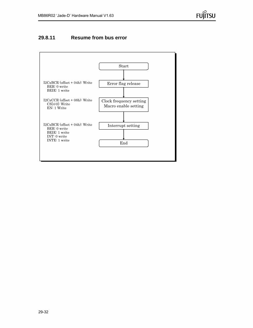
29-32
MB86R02 ‘Jade-D’ Hardware Manual V1.63
29.8.11 Resume from bus error
Start
Error flag release
Clock frequency settingMacro enable setting
Interrupt setting
End
I2CxBCR (offset + 04h): Write BER: 0 write BEIE: 1 write
I2CxCCR (offset + 08h): Write CS[4:0]: Write EN: 1 Write
I2CxBCR (offset + 04h): Write BER: 0 write BEIE: 1 write INT: 0 write INTE: 1 write

29-33
MB86R02 ‘Jade-D’ Hardware Manual V1.63
29.8.12 Interrupt process and wait request operation to master
When the INT flag of the I2CxBCR register is "H" (when this module generates an interrupt and the CPU proceeds with an interrupt operation), "L" is output to the SCL line. If the slave side sets "L" on the SCL line, the master side is unable to generate the next transfer so that slave side performs a wait on the master side.
29.9 Notes
System clock and fscl of this module The supply system clock to this module is within the following range. Communication with a system clock of 18MHz or more requires a corresponding I2CxCSR setting.
Master operation: 14MHz ~ 41.5MHz Set I2CxCCR so that it doesn't exceed the following limits on fscl. If it exceeds the upper limit of each mode, normal transfer is not executed as it careates a timing violation on the I2C bus.
Standard: 100kHz High-speed: 400kHz
Slave operation: 14MHz ~ 41.5MHz Register access: 14MHz ~ 41.5MHz
10 bit slave address This module does not support a 10 bit slave address. Therefore, do not specify a slave address from 78H to 7BH for the module. If a wrong address is specified, an acknowledge is returned on receiving 1byte however normal transfer will not proceed. Competition of the SCC, MSS and INT bits Simultaneous writing to the SCC, MSS, and INT bits causes competition between start and stop conditions on the next byte transfer. The priority in this case is as follows.
3. Occurrence of the next byte transfer and stop condition If a "0" is written to the INT bit and the MSS bit simultaneously, the MSS bit is prioritized and a stop condition occurs.
4. Occurrence of the next byte transfer and start condition If "0" is written to the INT bit and a "1" is written to the SCC bit simultaneously, the SCC bit is prioritized and a start condition occurs.
5. Occurrence of start condition and stop condition Writing a "1" to the SCC bit and "0" to the MSS bit simultaneously is prohibited.
Serial transfer clock setting If the rising edge delay of the SCL line is large or the clock is expanded for the slave device, the value may be smaller than the setting value (calculated value) as overhead occurs.

29-34
MB86R02 ‘Jade-D’ Hardware Manual V1.63
Restrictions in global call address transmission at using multi master If this module is used as a multimaster, it is prohibited for other masters to send a global call address at the same time as this module and it loses arbitration at the 2nd byte or later. The following usage does not fall under this restriction.
This module is used in a single master environment. This module is used in a multimaster environment, however it does not send a general call
address. This module is used in a multimaster environment, however other modules do not use a
general call address transmission. Although this module is used in a multimaster environment and other masters send general
call address simultaneously with this module, it does not lose arbitration at the 2nd byte or later.*
*: Because the larger transmission data causes an 'arbitration lost', the data of the 2nd byte or later must always be smaller than the value of the other masters' data.
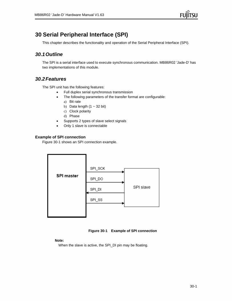
30-1
MB86R02 ‘Jade-D’ Hardware Manual V1.63
30 Serial Peripheral Interface (SPI) This chapter describes the functionality and operation of the Serial Peripheral Interface (SPI).
30.1 Outline
The SPI is a serial interface used to execute synchronous communication. MB86R02 'Jade-D' has two implementations of this module.
30.2 Features
The SPI unit has the following features: Full duplex serial synchronous transmission The following parameters of the transfer format are configurable:
a) Bit rate b) Data length (1 ~ 32 bit) c) Clock polarity d) Phase
Supports 2 types of slave select signals Only 1 slave is connectable
Example of SPI connection Figure 30-1 shows an SPI connection example.
Figure 30-1 Example of SPI connection
Note: When the slave is active, the SPI_DI pin may be floating.
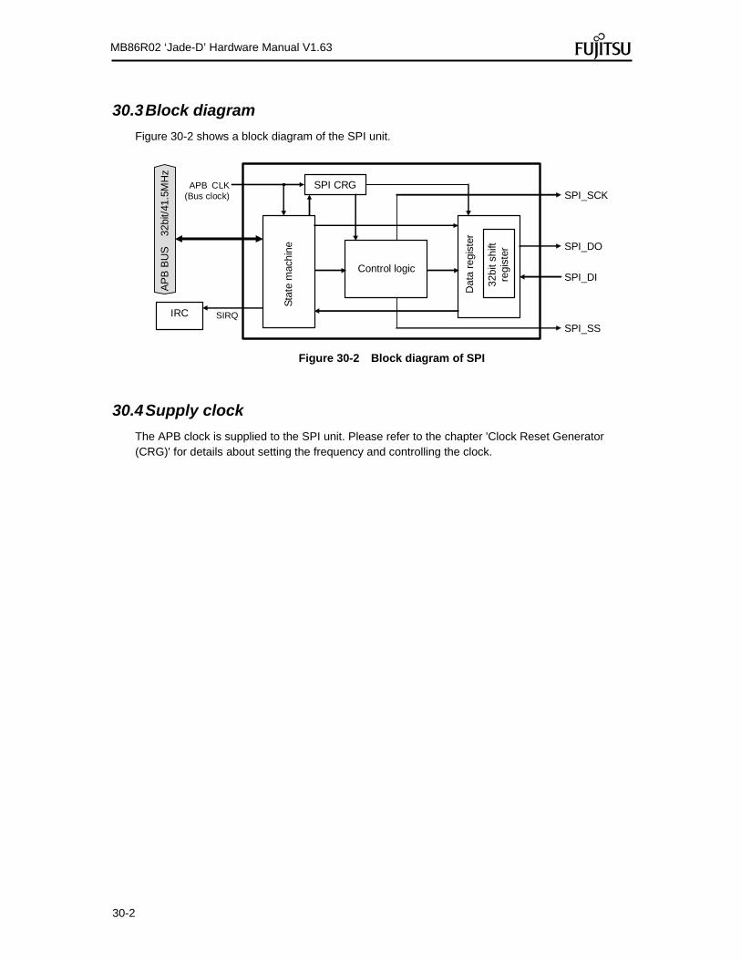
30-2
MB86R02 ‘Jade-D’ Hardware Manual V1.63
30.3 Block diagram
Figure 30-2 shows a block diagram of the SPI unit.
APB CLK (Bus clock)
SPI CRG
Sta
te m
achi
ne
Control logic
32bi
t shi
ft
regi
ster
Dat
a re
gist
er
AP
B B
US
32
bit/
41.5
MH
z
SIRQ
SPI_SCK
SPI_DO
SPI_DI
SPI_SS
IRC
Figure 30-2 Block diagram of SPI
30.4 Supply clock
The APB clock is supplied to the SPI unit. Please refer to the chapter 'Clock Reset Generator (CRG)' for details about setting the frequency and controlling the clock.

30-3
MB86R02 ‘Jade-D’ Hardware Manual V1.63
30.5 Transition state
Figure 30-3 shows SPI transition state chart.
RESET
SLEEP
SENB = 0 SBSY = 0 SERR = 0
ERROR
SENB = 1 SBSY = 0 SERR = 1
SETUP
SENB = 1 SBSY = 0 SERR = 0
BUSY
SENB = 1 SBSY = 1 SERR = 0
HRESETn = 1
SPE = 1
SPE = 0
Write data
Normal end
Error
SPE = 0
Figure 30-3 SPI state transition chart Detail of each state shown in Figure 30-3 is as follows. SPI moves to reset state with hardware reset (HRESETn = 0) from all conditions (broken line in the chart.)
SPI state Description
Sleep (SLEEP) Initial state of SPI. Clock is not supplied except to state machine. While setup or transition from error state,internal logic is initialized except certain part.
Setup (SETUP) Stand-by state of communication between master and slave. SPI changes state in the following cases. SPE bit of SPI slave control register (SPISCR) is set to "1" in the sleep state Communication completes properly in the busy state Received data should be read in the setup state.
Busy (BUSY) Communicating state with SPI slave. Writing SPI data register (SPIDR) in the setup state moves to this state; in that time, transmission/reception of the data are performed simultaneously. When 1 bit is output to SPI_DO pin, 1 bit is input from SPI_DI pin. Set SIRQ at the normal termination of the communication.
Error (ERROR) Performing prohibited register access in the busy state moves to this state. Clearing SPE bit of SPI slave control register (SPISCR) returns to sleep (SLEEP) state.
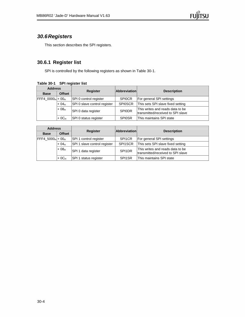
30-4
MB86R02 ‘Jade-D’ Hardware Manual V1.63
30.6 Registers
This section describes the SPI registers.
30.6.1 Register list
SPI is controlled by the following registers as shown in Table 30-1.
Table 30-1 SPI register list Address
Register Abbreviation Description Base Offset
FFF4_0000H + 00H SPI 0 control register SPI0CR For general SPI settings
+ 04H SPI 0 slave control register SPI0SCR This sets SPI slave fixed setting
+ 08H SPI 0 data register SPI0DR
This writes and reads data to be transmitted/received to SPI slave
+ 0CH SPI 0 status register SPI0SR This maintains SPI state
Address
Register Abbreviation Description Base Offset
FFF4_5000H + 00H SPI 1 control register SPI1CR For general SPI settings
+ 04H SPI 1 slave control register SPI1SCR This sets SPI slave fixed setting
+ 08H SPI 1 data register SPI1DR
This writes and reads data to be transmitted/received to SPI slave
+ 0CH SPI 1 status register SPI1SR This maintains SPI state

30-5
MB86R02 ‘Jade-D’ Hardware Manual V1.63
Description format of register Following format is used for description of register’s each bit in "30.6.2 SPI control register (SPInCR)" to "30.6.5 SPI status register (SPInSR)".
Address Base address + Offset Bit 31 30 29 28 27 26 25 24 23 22 21 20 19 18 17 16
Name R/W
Initial value Bit 15 14 13 12 11 10 9 8 7 6 5 4 3 2 1 0
Name R/W
Initial value
Meaning of item and sign Address
Address (base address + offset address) of the register Bit
Bit number of the register Name
Bit field name of the register R/W
Attribution of read/write of each bit field R0:Read value is always "0" R1: Read value is always "1" W0: Write value is always "0", and write access of "1" is ignored W1: Write value is always "1", and write access of "0" is ignored R: Read W: Write
Initial value Each bit field’s value after reset
0: Value is "0" 1: Value is "1" X: Value is undefined

30-6
MB86R02 ‘Jade-D’ Hardware Manual V1.63
30.6.2 SPI control register (SPInCR)
This register is to set common setting of SPI. SPICR setting should be carried out in the sleep or setup states, and do not write to this register in the busy state. Each bit of SPICR is not cleared even the state is changed to sleep by SPE = 0 of SPI slave control register (SPISCR.)
Address SPI0: FFF4_0000H + 00H
SPI1: FFF4_5000H + 00H Bit 31 30 29 28 27 26 25 24 23 22 21 20 19 18 17 16
Name – – – – – – – – – – – – – – – SPL0R/W R0 R0 R0 R0 R0 R0 R0 R0 R0 R0 R0 R0 R0 R/W R/W R/W
Initial value X X X X X X X X X X X X X 0 0 0 Bit 15 14 13 12 11 10 9 8 7 6 5 4 3 2 1 0
Name – – – – – CDV2 CDV1 CDV0 – – – – – – CPOL CPHAR/W R0 R0 R0 R0 R0 R/W R/W R/W R0 R0 R0 R0 R0 R0 R/W R/W
Initial value X X X X X 0 0 0 X X X X X X 0 0 (Note) This register should be accessed in 32 bit unit.
Bit field
Description No. Name
31-19 – Unused bits. The write access is ignored. The read value of these bits is always "0".
18-17 – Unused bits. The write access is ignored.
16 SPL0 Polarity of SPI_SS pin (slave selection pin) is specified.
0 Active-high (initial value)
1 Active-low
15-11 – Unused bits. The write access is ignored. The read value of these bits is always "0".
10-8 CDV2-0 Frequency dividing ratio of serial clock (SCK) to bus clock (PCLK) is specified.
CDV2 CDV1 CDV0 Frequency dividing ratio
0 0 0 PCLK 1/2 (initial value)
0 0 1 PCLK 1/4
0 1 0 PCLK 1/8
0 1 1 PCLK 1/16
1 0 0 PCLK 1/32
1 0 1 PCLK 1/64
1 1 0 PCLK 1/128
1 1 1 PCLK 1/256
7-2 – Unused bits. The write access is ignored. The read value of these bits is always "0".
1 CPOL Polarity of serial clock (SCK) is selected.
0 Positive pulse (initial value)
1 Negative pulse

30-7
MB86R02 ‘Jade-D’ Hardware Manual V1.63
Bit field Description
No. Name
0 CPHA Timing of I/O serial data (DI/DO) and serial clock (SCK) are specified. Timing at CPHA = 0 or 1, and CPOL = 0 is shown in Figure 30-4 Timing at CPHA = 0 or 1, and CPOL = 1 is shown in Figure 30-5
SPI_SCK (CPHA=0)
SPI_SCK (CPHA=1)
SPI_DI Shift in
SPI_DI Shift out
Bit7 Bit6 Bit5 Bit4 Bit3 Bit2 Bit1 Bit0
Figure 30-4 Timing of serial data and serial clock (at CPOL = 0)
SPI_SCK (CPHA=0)
SPI_SCK (CPHA=1)
SPI_DI Shift in
SPI_DI Shift out
Bit7 Bit6 Bit5 Bit4 Bit3 Bit2 Bit1 Bit0
Figure 30-5 Timing of serial data and serial clock (at CPOL = 1)

30-8
MB86R02 ‘Jade-D’ Hardware Manual V1.63
30.6.3 SPI slave control register (SPInSCR)
This register maintains unique setting of SPI slave. All bits are cleared by moving state to sleep. Set this register at sleep or setup state.
Address SPI0: FFF4_0000H + 04H
SPI1: FFF4_5000H + 04H Bit 31 30 29 28 27 26 25 24 23 22 21 20 19 18 17 16
Name – – – SPE – – – DRVS – – – – STL3 STL2 STL1 STL0R/W R0 R0 R0 R/W R0 R0 R0 R/W R0 R0 R0 R0 R/W R/W R/W R/W
Initial value X X X 0 X X X 0 X X X X 0 0 0 0 Bit 15 14 13 12 11 10 9 8 7 6 5 4 3 2 1 0
Name – – – DLN4 DLN3 DLN2 DLN1 DLN0 – – SMOD SAUT – – SSP1 SSP0R/W R0 R0 R0 R/W R/W R/W R/W R/W R0 R0 R/W R/W R0 R0 R/W R/W
Initial value X X X 0 0 0 0 0 X X 0 0 X X 0 0 (Note) This register should be accessed in 32 bit unit.
Bit field
Description No. Name
31-29 – Unused bits. The write access is ignored. The read value of these bits is always "0".
28 SPE SPI's clock supply is controlled.
0 Clock supply to internal logic stops except certain part (initial value)
1 Clock is supplied to all the circuits Write "1" to operate SPI. Its state changes from sleep to setup by setting SPE bit. It changes to sleep by clear; at the same time, internal logic is reset except certain part.
27-25 – Unused bits. The write access is ignored. The read value of these bits is always "0".
24 DRVS Transfer order of serial data is specified.
0 MSB --> LSB (initial value)
1 LSB --> MSB
27-25 – Unused bits. The write access is ignored. The read value of these bits is always "0".
19-16 STL3-0 Strobe width is specified at pulse mode selection (SMOD = 1) in the range of SCK 1 ~ 16 cycles.
0000 SCK 1cycle (initial value)
0001 SCK 2cycles
: :
1110 SCK 15cycles
1111 SCK 16cycles
15-13 – Unused bits. The write access is ignored. The read value of these bits is always "0".

30-9
MB86R02 ‘Jade-D’ Hardware Manual V1.63
Bit field Description
No. Name
12-8 DLN4-0 Data length of transmission/reception serial data is specified in the range of 1 ~ 32 bit.
00000 1 bit (initial value)
00001 2 bit
00010 3 bit
: :
11101 30 bit
11110 31 bit
11111 32 bit
7-6 – Unused bits. The write access is ignored. The read value of these bits is always "0".
5 SMOD Operation mode of slave selection is specified. Slave selection signal is output to SPI_SS pin.
0 Selection mode (always active while communication) (initial value)
1 Pulse mode (after communicating, this becomes active)
4 SAUT Operation timing of slave selection is specified according to the combination of SMOD bit.
0 Slave selection synchronizes with SSP bit's setting value regardless of SMOD (see Figure 30-6) (initial value)
1 1SCK of wait is added from SPI data register (SPIDR) writing to serial data transmission, and from the last data transmission to asserting/negating salve selection (see Figure 30-7)
3-2 – Unused bits. The write access is ignored. The read value of these bits is always "0".
1-0 SSP1-0 Slave selection pin to be active is specified.
00 Slave selection pin becomes non-active (initial value)
01 SPI_SS pin becomes active
10 Reserved (setting prohibited)
11 Reserved (setting prohibited)

30-10
MB86R02 ‘Jade-D’ Hardware Manual V1.63
First Last
SIRQ
SPI_SS
SPI_DO
SSP Assert
SPIDR Write
SSP Negate
SPISR Read
BUSY
Figure 30-6 Timing chart of SPI_SS pin (at SAUT = 0)
First Last
SIRQ
SPI_SS SMOD=0
DPI_DO
SPIDR Write
BUSY
1SCK 1SCK
SIRQ
SPI_SS SMOD=1
STL
BUSY
Figure 30-7 Timing chart of SPI_SS pin (at SAUT = 1)

30-11
MB86R02 ‘Jade-D’ Hardware Manual V1.63
30.6.4 SPI data register (SPInDR)
This register is used to write/read data to be transmitted to/received from SPI slave.
Address SPI0: FFF4_0000H + 08H
SPI1: FFF4_5000H + 08H Bit 31 30 29 28 27 26 25 24 23 22 21 20 19 18 17 16
Name D31 D30 D29 D28 D27 D26 D25 D24 D23 D22 D21 D20 D19 D18 D17 D16R/W R/W R/W R/W R/W R/W R/W R/W R/W R/W R/W R/W R/W R/W R/W R/W R/W
Initial value 0 0 0 0 0 0 0 0 0 0 0 0 0 0 0 0 Bit 15 14 13 12 11 10 9 8 7 6 5 4 3 2 1 0
Name D15 D14 D13 D12 D11 D10 D9 D8 D7 D6 D5 D4 D3 D2 D1 D0 R/W R/W R/W R/W R/W R/W R/W R/W R/W R/W R/W R/W R/W R/W R/W R/W R/W
Initial value 0 0 0 0 0 0 0 0 0 0 0 0 0 0 0 0 (Note) This register should be accessed in 32 bit unit. Do not operate this register in the busy state.
Bit field
Description No. Name
31-0 D31-0 Transmission/Reception data to SPI slave is stored. SPIDR is reset at moving to the sleep state. Writing to this register in the setup state starts transmission/reception of the data length specified in DLN[4:0] bit of SPI slave control register (SPISCR), and LSB is fixed regardless of the data length.

30-12
MB86R02 ‘Jade-D’ Hardware Manual V1.63
30.6.5 SPI status register (SPInSR)
This register is to maintain SPI state, and it is not able to be written.
Address SPI0: FFF4_0000H + 0CH
SPI1: FFF4_5000H + 0CH Bit 31 30 29 28 27 26 25 24 23 22 21 20 19 18 17 16
Name – – – – – – – – – – – – – – – – R/W R0 R0 R0 R0 R0 R0 R0 R0 R0 R0 R0 R0 R0 R0 R0 R0
Initial value X X X X X X X X X X X X X X X X Bit 15 14 13 12 11 10 9 8 7 6 5 4 3 2 1 0
Name – – – – – – – – SIRQ – – – – SER
R SBS
Y SEN
B R/W R0 R0 R0 R0 R0 R0 R0 R0 R R R R R R R R
Initial value X X X X X X X X 0 X X X X 0 0 0 (Note) This register should be accessed in 32 bit unit
Bit field
Description No. Name
31-8 – Unused bits. The write access is ignored. The read value of these bits is always "0".
7 SIRQ Proper completion of communication between master slaves is indicated.
0 It is under the communication or stand-by (initial value)
1 Communication is completed SIRQ pin outputs this bit. It is cleared by reading SPISR register. Figure 30-6 and Figure 30-7 show timing chart.
6-3 – Unused bits. The write access is ignored. The read value of these bits is always "0".
2 SERR Operation error is indicated.
0 Normal operation is in process (initial value)
1 Prohibited operation occurs Clear SPE bit of SPI slave control register (SPISCR)
SERR bit is set to "1" by processing other operations than reading SPICR, SPISCR, and SPISR in the busy state. Moreover, this bit is cleared by changing state to sleep with clearing SPE bit of SPISCR.
1 SBSY Communication with SPI slave is in process.
0 It is standing-by (initial value)
1 It is communicating SBSY is set to "1" by writing to SPI data register (SPIDR.) Do not clear SPE bit of SPISCR in the busy state. This bit is released by either of followings: SIRQ bit setting SERR bit setting
0 SENB Enables/disable SPI unit
0 Disable SPI
1 Enable SPI
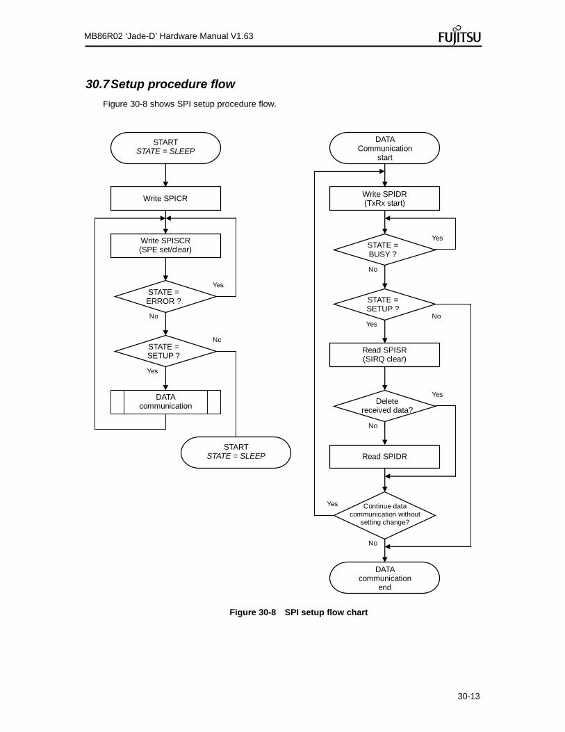
30-13
MB86R02 ‘Jade-D’ Hardware Manual V1.63
30.7 Setup procedure flow
Figure 30-8 shows SPI setup procedure flow.
START STATE = SLEEP
Yes
No
STARTSTATE = SLEEP
STATE = ERROR ?
Write SPISCR (SPE set/clear)
Write SPICR
STATE = SETUP ?
DATA communication
No
Yes
Yes
No
STATE = BUSY ?
Read SPISR (SIRQ clear)
Write SPIDR (TxRx start)
STATE = SETUP ?
No
Yes
DATA Communication
start
Delete
received data?
Read SPIDR
Continue data
communication without setting change?
DATA
communication end
Yes
No
Yes
No
Figure 30-8 SPI setup flow chart

31-1
MB86R02 ‘Jade-D’ Hardware Manual V1.63
31 CAN Interface (CAN) This chapter describes the CAN interface of the MB86R02. Please refer to the following website for the CAN module specification. URL: http://www.semiconductors.bosch.de/en/ipmodules/can/canipmodules/c_can/c_can.asp
31.1 Outline
MB86R02 incorporates a 2 port CAN interface which is in compliance with CAN protocol version 2.0 part A and B.
31.2 Block diagram
Figure 31-1 shows a block diagram of the CAN module.
APB Slave
APB bus
0ch
I/O port
MB86R02
CAN core
CAN_TX0 and CAN_RX0
APB Slave
I/O port
CAN core
CAN_TX1 and CAN_RX1
1ch
IRC
Figure 31-1 CAN Block diagram

31-2
MB86R02 ‘Jade-D’ Hardware Manual V1.63
31.3 Supply clock
The APB clock is supplied to the CAN interface. Please refer to "Clock Reset generator (CRG)" for information about setting the frequency and the control specifications of this clock.
31.4 Registers
The register mapping of this GDC is in byte addresses (8 bit). 16 bit length registers are allocated by word address units (32 bit) for the local address of CAN; thus the valid data in 32 bit width data of the APB Bus is 16 bit.
Table 31-1 CAN 0ch register map Register address CAN 0ch register address APB Bus data[31:0]
FFF5_4000h 00h 0x0000, 16 bit data
FFF5_4004h 02h 0x0000, 16 bit data
FFF5_4008h 04h 0x0000, 16 bit data
Table 31-2 CAN 1ch register map Register address CAN 1ch register address APB Bus data [31:0]
FFF5_5000h 00h 0x0000, 16 bit data
FFF5_5004h 02h 0x0000, 16 bit data
FFF5_5008h 04h 0x0000, 16 bit data
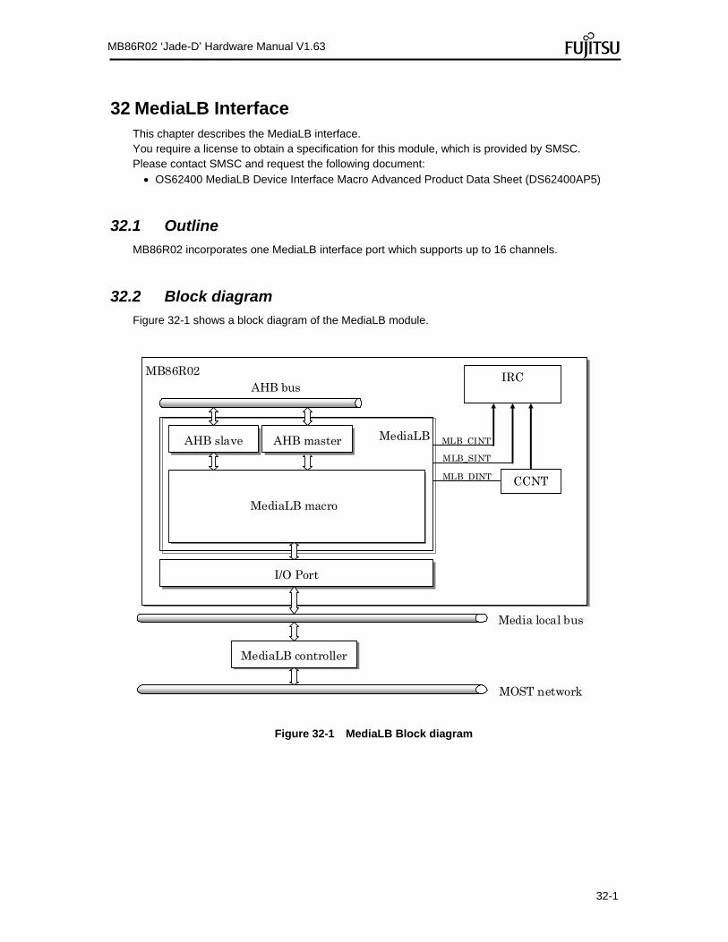
32-1
MB86R02 ‘Jade-D’ Hardware Manual V1.63
32 MediaLB Interface This chapter describes the MediaLB interface. You require a license to obtain a specification for this module, which is provided by SMSC. Please contact SMSC and request the following document: OS62400 MediaLB Device Interface Macro Advanced Product Data Sheet (DS62400AP5)
32.1 Outline
MB86R02 incorporates one MediaLB interface port which supports up to 16 channels.
32.2 Block diagram
Figure 32-1 shows a block diagram of the MediaLB module.
AHB slave
AHB bus
MediaLB
I/O Port
MB86R02
AHB master
MediaLB macro
Media local bus
MediaLB controller
MOST network
IRC
MLB_CINT
MLB_SINT
MLB_DINT CCNT
Figure 32-1 MediaLB Block diagram

32-2 FUJITSU PROPRIETARY AND CONFIDENTIAL - DRAFT
MB86R02 ‘Jade-D’ Hardware Manual V1.63
32.3 Supply clock
The AHB clock signal is supplied to the MediaLB interface module. Please refer to "5. Clock reset generator (CRG)" for information about setting the frequency and the control specifications of the AHB clock.
32.4 Registers
The registers of this GDC are mapped in byte addresses (8 bit), however local addresses of the MediaLB module are accessed using word addresses (32 bit).
Register address MediaLB local address
FFF6_0000h 00h
FFF6_0004h 01h
FFF6_0008h 02h
33-1
MB86R02 ‘Jade-D’ Hardware Manual V1.63
33 SD Memory Controller (SDMC) Only SD card licensees can be given this information. Please contact us at: https://www-s.fujitsu.com/emea/services/microelectronics/gdc/gdc-enquiryform/index.html for details.

34-1
MB86R02 ‘Jade-D’ Hardware Manual V1.63
34 Electrical Characteristics1
34.1 Maximum Ratings
Parameter Symbol Rating Unit
Supply voltage VDDI, PVD(=PLL VDD) SVD(=SSCG VDD), APIXVD12(= APIXVDD 1.2V)
-0.5 to 1.8 (*1) V
VDDE, APIXVD33(= APIXVDD 3.3V)
-0.5 to 4.0 (*2) V
DDRVDE -0.5 to 2.5 (*3) V
Input voltage VI -0.5 to VDDI + 0.5 (< 1.8V) -0.5 to VDDE + 0.5 (< 4.0V)-0.5 to DDRVDE + 0.5 (< 2.5V)
V
Output voltage VO -0.5 to VDDI + 0.5 (< 1.8V) -0.5 to VDDE + 0.5 (< 4.0V)-0.5 to DDRVDE + 0.5 (< 2.5V)
V
Storage temperature TST -55 to 125 C
Junction temperature TJ -40 to 125 C
Output current IO TBD mA
Supply current ID TBD mA
*1: Power supply for internal part or PLL *2: Power supply for I/O part *3: Power supply for SSTL_18 I/O part
Table 34-1 Maximum Ratings Note:
Exceeding the maximum ratings (voltage, current, temperature, etc.) may cause damage to semiconductor devices. Never exceed the ratings above.
Do not connect an IC output or I/O pin directly or connect them to VDD or VSS directly as the thermal destruction of elements might occur (except for those pins designed for output timing).
Provide ESD protection, such as grounding when handling the product; otherwise an externally-generated electric charge could flow into the IC and cause circuit destruction.
Applying voltages higher than VDD or lower than VSS to I/O pins of this CMOS IC, or applying voltage higher than the ratings between VDD and VSS can cause latch-up. The latch up increases supply current, resulting in the thermal destruction of elements. When handling the product, never exceed the maximum ratings.
1 RSDS to be added, other values from MB86R01 to be confirmed (validation ongoing)

34-2
MB86R02 ‘Jade-D’ Hardware Manual V1.63
Parameter Symbol Rating Unit
Supply voltage AD_AVD0 -0.5 to 4.0 V
Input voltage AD_VRH0 AD_VRH1 AD_VRL0 AD_VRL1 AD_VIN0 AD_VIN1 AD_VIN2 AD_VIN3
-0.5 to VDDE + 0.5 (< 4.0V)
V
Output voltage AD_VR0 AD_VR1
-0.5 to VDDE + 0.5 (< 4.0V) V
Junction temperature TJ -40 to 125 C
Table 34-2 ADC Maximum Ratings
34.2 Recommended Operating Conditions
Parameter Symbol Rating
Unit Min. Typ. Max.
Power supply voltage
VDDI, PVD, SVD, APIXVD12 (= APIXVDD 1.2V)
1.1 1.2 1.3 V
VDDE, APIXVD33 (= APIXVDD 3.3V)
3.0 3.3 3.6 V
Input voltage (High level)
3.3V CMOS VIH 2.0 – VDDE + 0.3 V
Input voltage (Low level)
3.3V CMOS VIL -0.3 – 0.8 V
Operating ambient temperature TA -40 – 105 C
Junction temperature TJ -40 – 125 C
Table 34-3 3.3V Standard CMOS I/O Recommended Operating Conditions
Parameter Symbol Min. Typ. Max. Unit
Power supply voltage VDE (DDRVDE) 1.7 1.8 1.9 V
VDDI 1.10 1.20 1.30 V
Junction temperature TJ -40 – 125 C
The recommended operating conditions for the standard SSTL_18 (excerpted from JESD8-15a).
Table 34-4 SSTL_18 Recommended Operating Conditions
Note: The recommended operating conditions are primarily intended to ensure the normal operation of semiconductor device. The values of electrical characteristics are guaranteed under the requirements above, so use the product accordingly. Using the product without observing the conditions may affect the product's reliability. Performance of this product is not guaranteed using under the unspecified conditions and unspecified combination of logic. Be sure to contact Fujitsu when using the product under such conditions.

34-3
MB86R02 ‘Jade-D’ Hardware Manual V1.63
34.3 Precautions at Power On
34.3.1 Recommended Power On/Off Sequence
Follow the power on/off sequence as shown below: <ON>: VDDI (internal and PLLVDD) + APIXVD12 VDDE (external) + APIXVD33 DDRVDE (external) + APIXVD12 Signal <OFF>: Signal VDDE (external) DDRVDE (external) VDDI (internal and PLLVDD) + APIXVD12
VDDI,
APIXVD12
VDDE,
APIXVD33
DDRVDE
Figure 34-1 Recommended Power On/Off Sequence (1) There is no limitation on the sequence of power on/off of VDDI, VDDE, and DDRVDE if the following condition is met. (Figure 34-2) Do not apply VDDE and DDRVDE (external) continuously for more than 1 second when VDDI
(internal) is off.
VDDE,
APIXVD33
1 sec. or less
VDDI,
APIXVD12
1 sec. or less
DDRVDE
Figure 34-2 Recommended Power On/Off Sequence (2) Perform power on/off for VREF according to the DDR2-SDRAM regulation. Perform power on/off so that power for PLLVDD (PLL) does not exceed VDDI. Turn on all power. Turning on only a part of them is prohibited. CMOS IC becomes unstable immediately after power-on so execute a reset immediately.2 Set the reset pins (XTRST and XRST) to Low when power-on. Input clock to ECLK pin immediately after power-on.
2 If an external clock signal is used.

34-4
MB86R02 ‘Jade-D’ Hardware Manual V1.63
It requires at least 100 clocks (input clock to CLK pin) for the reset signal "L" applied to the XRST pin to be transmitted to all internal circuits.
34.3.2 Power On Reset
VDDE (external)
DDRVDE (DRAM)
XRST
XTRST
Note: Clock is just an image, not the actual one.
Internal
clock generated by
ECLK or XTAL
Input "L" wh en power-on
Input clock immediate ly
after power-on
PLL Lockup Time
VDDI (internal)
Input "L" wh en power-on
8 s or more
XSRST output "L" when power-on
Input when XRST is "H" after "L"
Figure 34-3 Power On Sequence Input XTRST and XRST pins to Low when power-on. Keep XTRST and XRST pins High after setting to Low level for 8s or more. Access the other registers or memory controller after PLL Lockup Time.

34-5
MB86R02 ‘Jade-D’ Hardware Manual V1.63
34.4 DC Characteristics
34.4.1 3.3V Standard CMOS I/O
Table 34-5 shows 3.3V standard CMOS I/O DC characteristics.
Table 34-5 Standard CMOS I/O DC Characteristics Measurement condition: VDDE = 3.3 0.3V, VSS = 0V, TJ = -40 to 125C
Parameter Symbol Condition Rating
UnitMin. Typ. Max.
H level input voltage
VIH 2.0 – VDDE +0.3 V
L level input voltage
VIL -0.3 – 0.8 V
H level output voltage
VOH IOH = -100A VDDE - 0.2 – VDDE V
L level output voltage
VOL IOL = 100A 0 – 0.2 V
H level output V-I characteristic
–
Driving capability 1 IOH = 4mA
See Figure 34-4, Figure 34-5, and Figure 34-6 characteristics
– Driving capability 2 IOH = 6mA
Driving capability 3 IOH = 8mA
L level output V-I characteristic
–
Driving capability 1 IOL = 4mA
– Driving capability 2 IOL = 6mA
Driving capability 3 IOL = 8mA
Input leakage current
IL – – 4 A
Driving capabilities 1 to 3 in the table above indicate the following external pins:
Driving capability 1: MEM_ED_0, MEM_ED_1, MEM_ED_2, MEM_ED_3, MEM_ED_4, MEM_ED_5, MEM_ED_6, MEM_ED_7, MEM_ED_8, MEM_ED_9, MEM_ED_10, MEM_ED_11, MEM_ED_12, MEM_ED_13, MEM_ED_14, MEM_ED_15, MEM_EA_1, MEM_EA_2, MEM_EA_3, MEM_EA_4, MEM_EA_5, MEM_EA_6, MEM_EA_7, MEM_EA_8, MEM_EA_9, MEM_EA_10, MEM_EA_11, MEM_EA_12, MEM_EA_13, MEM_EA_14, MEM_EA_15, MEM_EA_16, MEM_EA_17, MEM_EA_18, MEM_EA_19, MEM_EA_20, MEM_EA_21, MEM_EA_22, MEM_EA_23, MEM_EA_24, MEM_XWR_0, MEM_XWR_1, MEM_XRD, MEM_XCS_0, MEM_XCS_2, MEM_XCS_4, MEM_RDY, TDO
Driving capability 2: TRACECLK, VSYNC1, DE1, HSYNC1, DOUTB1_3, DOUTB1_7, GV1,
DOUTB1_2, DOUTB1_6, DOUTG1_5, DOUTB1_5, DOUTG1_4,
DOUTB1_4, DOUTR1_3, DOUTG1_3, DOUTG1_2, DOUTR1_2,
DOUTG1_7, DOUTR1_7, DOUTG1_6, DOUTR1_6, DOUTR1_5,
DOUTR1_4, TSG_4, VSYNC0, GV0, DE0, TSG_6, HSYNC0, TSG_7,
TSG_10, TSG_5, TSG_8, TSG_11, VIN0_4, TSG_9, TSG_12, VIN0_5,
VIN0_0, VIN0_6, VINFID0, VIN0_1, VINHSYNC0, VIN0_2, VIN0_7,
VINVSYNC0, VIN0_3, VIN1_7, VINFID1, VIN1_6, VIN1_3, VIN1_5,
VIN1_4, VIN1_2, VIN1_1, VIN1_0, VINVSYNC1, MLB_SIG, MLB_DAT,
I2S_WS, I2S_SDO, I2S_SCK, I2S_ECLK, CAN_RX1, CAN_TX1,
CAN_RX0, CAN_TX0, PWM_O3, PWM_O2, PWM_O1, PWM_O0,

34-6
MB86R02 ‘Jade-D’ Hardware Manual V1.63
HOST_SPI_SCK, HOST_SPI_DI, HOST_SPI_DO, HOST_SPI_SS,
UART_SIN0, UART_SOUT0, UART_SIN1, UART_XCTS0,
UART_SOUT1, SPI_DI0, UART_XRTS0, UART_SIN2, SPI_DO0,
SPI_DI1, UART_SOUT2, SPI_SS0, SPI_DO1, SPI_SS1, SPI_SCK0,
SPI_SCK1, RTCK, XSRST, TRACEDATA_0, TRACECTL,
TRACEDATA_1, TRACEDATA_2, TRACEDATA_3
In LV-TTL Mode: DISP1P, DISP1N,…,DISP11P,DISP11N, DCLKP,
DCLKN
Driving capability 3: DCLKO1

34-7
MB86R02 ‘Jade-D’ Hardware Manual V1.63
34.4.1.1 3.3V Standard CMOS I/O V-I Characteristic (Driving Capability 1)
Conditions MIN: Process = Slow TJ = 125C VDDE = 3.0 V
TYP: Process = Typical TJ = 25C VDDE = 3.3 V
MAX: Process = Fast TJ = -40C VDDE = 3.6 V
Figure 34-4 3.3V Standard CMOS I/O V-I Characteristic (Driving Capability 1)
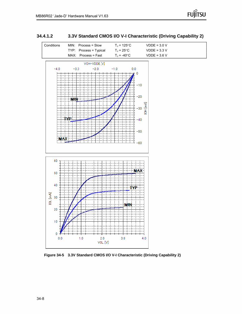
34-8
MB86R02 ‘Jade-D’ Hardware Manual V1.63
34.4.1.2 3.3V Standard CMOS I/O V-I Characteristic (Driving Capability 2)
Conditions MIN: Process = Slow TJ = 125C VDDE = 3.0 V
TYP: Process = Typical TJ = 25C VDDE = 3.3 V
MAX: Process = Fast TJ = -40C VDDE = 3.6 V
Figure 34-5 3.3V Standard CMOS I/O V-I Characteristic (Driving Capability 2)
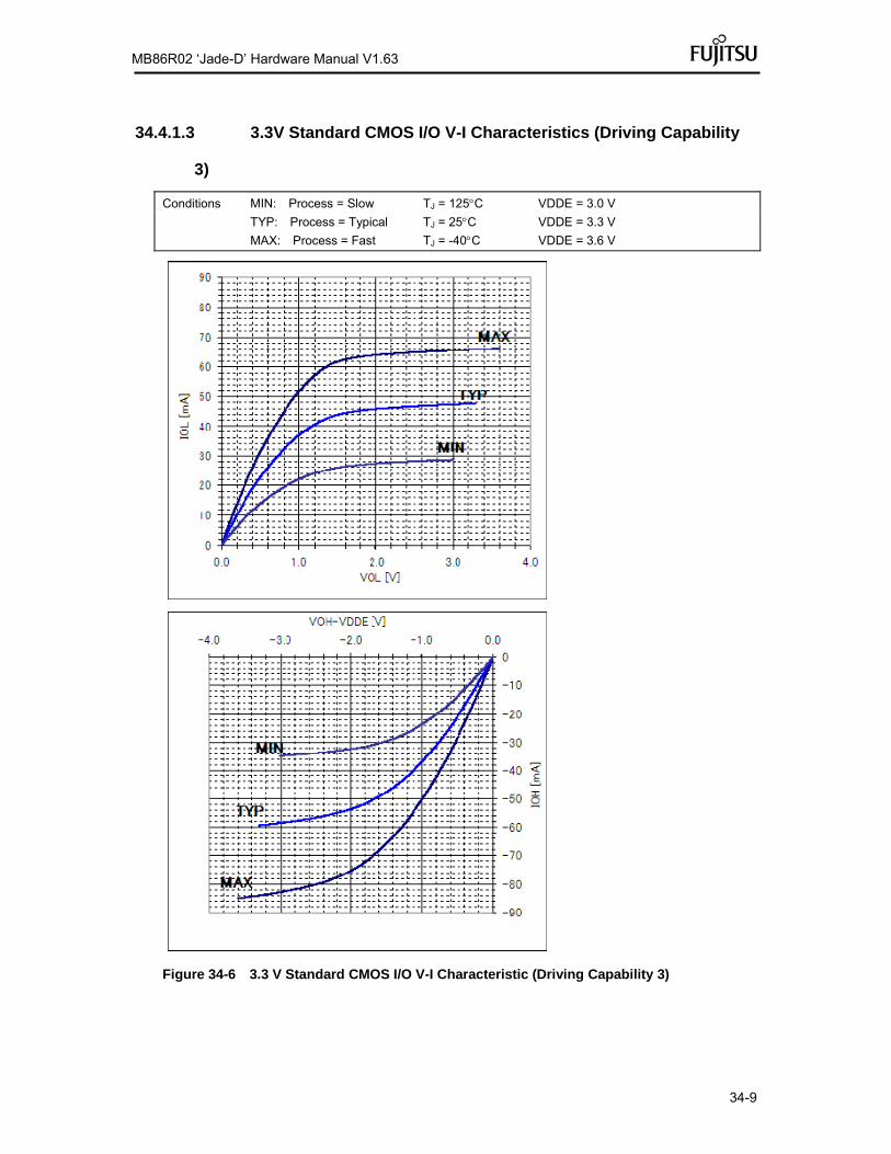
34-9
MB86R02 ‘Jade-D’ Hardware Manual V1.63
34.4.1.3 3.3V Standard CMOS I/O V-I Characteristics (Driving Capability
3)
Conditions MIN: Process = Slow TJ = 125C VDDE = 3.0 V
TYP: Process = Typical TJ = 25C VDDE = 3.3 V
MAX: Process = Fast TJ = -40C VDDE = 3.6 V
Figure 34-6 3.3 V Standard CMOS I/O V-I Characteristic (Driving Capability 3)

34-10
MB86R02 ‘Jade-D’ Hardware Manual V1.63
34.4.2 DDR2SDRAM IF I/O (SSTL_18)
SSTL_18 DC characteristics (an excerpt from JESD8-15a).
Table 34-6 SSTL18 Input DC Logic Levels (Single Ended) Symbol Parameter Min. Max. Unit
VIH (DC) DC input logic High VREF + 125 VDDQ + 300 mV
VIL (DC) DC input logic Low -300 VREF - 125 mV
Table 34-7 SSTL18 Input AC Logic Levels (Single Ended) Symbol Parameter Min. Max. Unit
VIH (AC) AC input logic High VREF + 250 – mV
VIL (AC) AC input logic Low – VREF - 250 mV
Table 34-8 SSTL18 Input AC Test Conditions (Single Ended) Symbol Condition Value Unit
VREF Input reference voltage 0.5 VDDQ V
VSWING (max.) Input single maximum peak to peak swing 1.0 V
SLEW Input single minimum slew rate 1.0 V/ns
Table 34-9 SSTL18 Input DC Logic Levels (Differential Ended) Symbol Parameter Min. Max. Unit
VIN (DC) DC input signal voltage -300 VDDQ + 300 mV
VID (DC) DC differential input voltage 250 VDDQ + 600 mV
Table 34-10 SSTL18 Input AC Logic Levels (Differential Ended) Symbol Parameter Min. Max. Unit
VID (AC) AC differential input voltage 500 VDDQ + 600 mV
VIX (AC) AC differential cross point voltage 0.5 VDDQ-175 0.5 VDDQ + 175 mV
Table 34-11 SSTL18 Input AC Test Conditions (Differential Ended) Symbol Parameter Min. Max. Unit
Vr Input timing measurement reference level
VIX (cross point)V
VSWING Input signal peak to peak swing voltage
– 1.0 V
SLEW Input signal slew rate 1.0 – V/ns
Table 34-12 SSTL18 Output DC Current Drive
Symbol Parameter Min. Max. Unit Note
s
IOH (DC) Output minimum source DC current
-11.4 (*3) – mA (*1)
IOL (DC) Output minimum sink DC current 11.4 (*3) – mA (*2)
*1: VDDQ = 1.7V, VOUT = 1420mV *2: VDDQ = 1.7V, VOUT = 280mV *3: The value is different from JESD8-15a. (JESD8-15a: 13.4mA)

34-11
MB86R02 ‘Jade-D’ Hardware Manual V1.63
Table 34-13 SSTL18 Differential AC parameters Symbol Parameter Min. Max. Unit
VOX AC differential cross point voltage 0.5 × VDDQ - 125 0.5 × VDDQ + 125 mV
Note:
External pin for DDR2SDRAM IO buffer is as follows. MDQSP[3:0], MDQSN[3:0], MDM[3:0], MDQ[31:0], MCKP, MCKN, MA[13:0], MBA[1:0], MCAS, MCKE, MCS, MRAS, MWE, ODTCONT, OCD, ODT, VREF0, VREF1
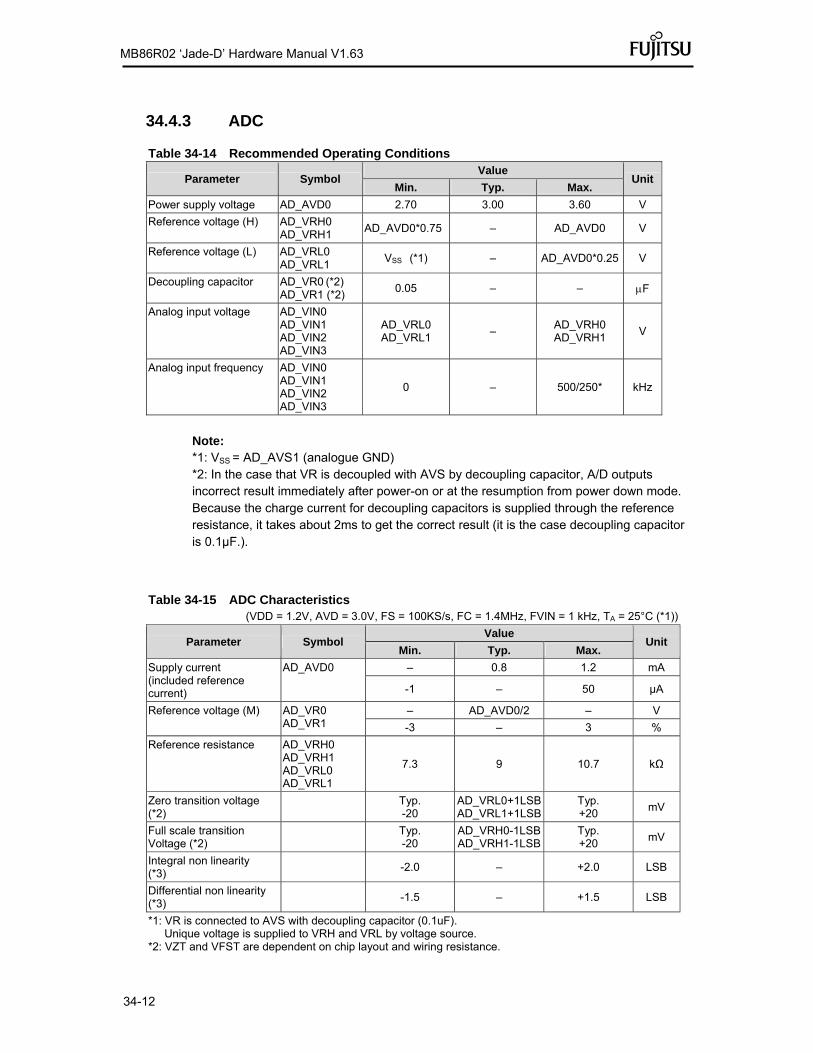
34-12
MB86R02 ‘Jade-D’ Hardware Manual V1.63
34.4.3 ADC
Table 34-14 Recommended Operating Conditions
Parameter Symbol Value
Unit Min. Typ. Max.
Power supply voltage AD_AVD0 2.70 3.00 3.60 V
Reference voltage (H) AD_VRH0 AD_VRH1
AD_AVD0*0.75 – AD_AVD0 V
Reference voltage (L) AD_VRL0 AD_VRL1
VSS (*1) – AD_AVD0*0.25 V
Decoupling capacitor AD_VR0 (*2) AD_VR1 (*2)
0.05 – – F
Analog input voltage AD_VIN0 AD_VIN1 AD_VIN2 AD_VIN3
AD_VRL0 AD_VRL1
– AD_VRH0 AD_VRH1
V
Analog input frequency AD_VIN0 AD_VIN1 AD_VIN2 AD_VIN3
0 – 500/250* kHz
Note: *1: VSS = AD_AVS1 (analogue GND) *2: In the case that VR is decoupled with AVS by decoupling capacitor, A/D outputs incorrect result immediately after power-on or at the resumption from power down mode. Because the charge current for decoupling capacitors is supplied through the reference resistance, it takes about 2ms to get the correct result (it is the case decoupling capacitor is 0.1µF.).
Table 34-15 ADC Characteristics (VDD = 1.2V, AVD = 3.0V, FS = 100KS/s, FC = 1.4MHz, FVIN = 1 kHz, TA = 25°C (*1))
Parameter Symbol Value
Unit Min. Typ. Max.
Supply current (included reference current)
AD_AVD0 – 0.8 1.2 mA
-1 – 50 µA
Reference voltage (M) AD_VR0 AD_VR1
– AD_AVD0/2 – V
-3 – 3 %
Reference resistance AD_VRH0 AD_VRH1 AD_VRL0 AD_VRL1
7.3 9 10.7 kΩ
Zero transition voltage (*2)
Typ. -20
AD_VRL0+1LSB AD_VRL1+1LSB
Typ. +20
mV
Full scale transition Voltage (*2)
Typ. -20
AD_VRH0-1LSB AD_VRH1-1LSB
Typ. +20
mV
Integral non linearity (*3)
-2.0 – +2.0 LSB
Differential non linearity (*3)
-1.5 – +1.5 LSB
*1: VR is connected to AVS with decoupling capacitor (0.1uF). Unique voltage is supplied to VRH and VRL by voltage source.
*2: VZT and VFST are dependent on chip layout and wiring resistance.

34-13
MB86R02 ‘Jade-D’ Hardware Manual V1.63
*3: 1LSB = (VFST-VZT)/1022, INLn = ((1LSBxn + VZT) - Vn)/1LSB, DNLn = (Vn + 1 -Vn)/1LSB - 1

34-14
MB86R02 ‘Jade-D’ Hardware Manual V1.63
34.4.4 I2C Bus Fast Mode I/O
Table 34-16 I2C I/O DC Characteristics
Parameter & Condition SymbolStandard Mode Fast Mode (*1)
Unit Min. Max. Min. Max.
"L" level input voltage VIL -0.5 0.3 VDDE -0.5 0.3 VDDE V
"H" level input voltage VIH 0.7 VDDE (*2) 0.7 VDDE (*2) V
Schmitt trigger hysteresis VDDE > 2[v]
Vhys n/a n/a 0.05 VDDE – V
"L" level output voltage Sink current 3[mA] VDDE > 2[v]
VOL1 0 0.4 0 0.4 V
Output slew rate (Tfall) Bus capacitance 10[pF] ~ 400[pF] VIH (min.) to VIL (max.)
tof – 250
20 + 0.1Cb
(*3) 250
ns
Data line leakage Input voltage 0.1 ~ 0.9 VDDE (max.)
Ii -10 10 -10 10 A
I/O pin capacitance Ci – 10 – 10 pF
*1: The I2C Bus Fast Mode I/O buffer is downward compatible with standard mode. *2: 90nm Technology: Complies with the maximum ratings 4[V]. *3: Cb: Capacitance for 1 bus line (Unit: pF). *4: The I2C Bus Fast Mode I/O buffer itself has no function to prevent spike of 50ns pulse width (max.).
Therefore, provide any input filter to prevent spike for both internal and external semiconductor device.
Note:
External pin for I2C IO buffer is as follows. I2C_SCL0, I2C_SDA0, I2C_SCL1, I2C_SDA1

34-15
MB86R02 ‘Jade-D’ Hardware Manual V1.63
34.4.4.1 I2C IO V-1 Characteristic Figure
Voltage (V)
Cu
rren
t (A
)
Figure 34-7 I2C V-I Characteristic Figure
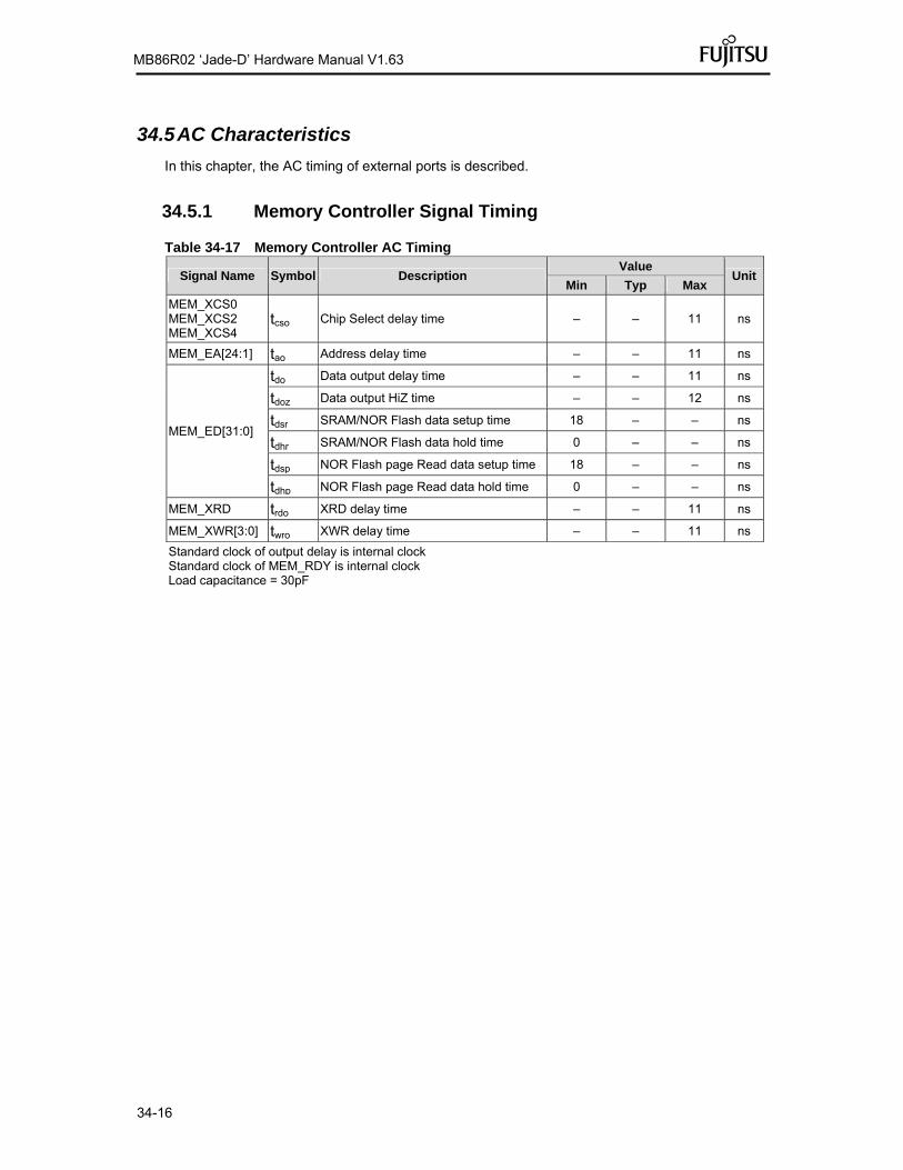
34-16
MB86R02 ‘Jade-D’ Hardware Manual V1.63
34.5 AC Characteristics
In this chapter, the AC timing of external ports is described.
34.5.1 Memory Controller Signal Timing
Table 34-17 Memory Controller AC Timing
Signal Name Symbol Description Value
Unit Min Typ Max
MEM_XCS0 MEM_XCS2 MEM_XCS4
tcso Chip Select delay time – – 11 ns
MEM_EA[24:1] tao Address delay time – – 11 ns
MEM_ED[31:0]
tdo Data output delay time – – 11 ns
tdoz Data output HiZ time – – 12 ns
tdsr SRAM/NOR Flash data setup time 18 – – ns
tdhr SRAM/NOR Flash data hold time 0 – – ns
tdsp NOR Flash page Read data setup time 18 – – ns
tdhp NOR Flash page Read data hold time 0 – – ns
MEM_XRD trdo XRD delay time – – 11 ns
MEM_XWR[3:0] twro XWR delay time – – 11 ns
Standard clock of output delay is internal clock Standard clock of MEM_RDY is internal clock Load capacitance = 30pF

34-17
MB86R02 ‘Jade-D’ Hardware Manual V1.63
Figure 34-8 SRAM/NOR Flash Read
Figure 34-9 SRAM/NOR Flash Write
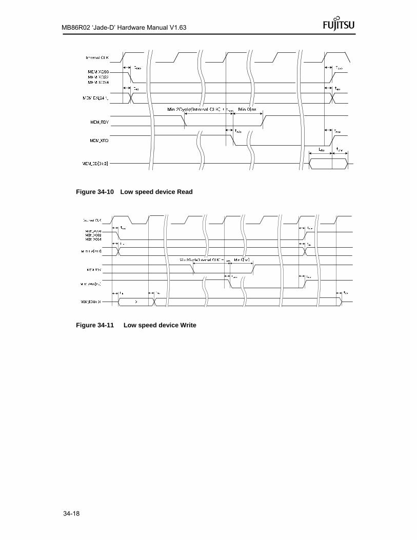
34-18
MB86R02 ‘Jade-D’ Hardware Manual V1.63
Figure 34-10 Low speed device Read
Figure 34-11 Low speed device Write
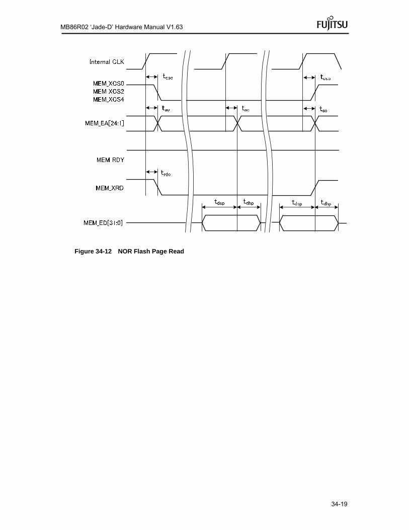
34-19
MB86R02 ‘Jade-D’ Hardware Manual V1.63
Figure 34-12 NOR Flash Page Read
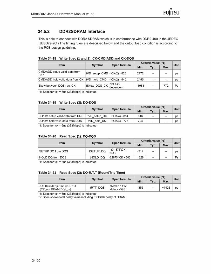
34-20
MB86R02 ‘Jade-D’ Hardware Manual V1.63
34.5.2 DDR2SDRAM Interface
This is able to connect with DDR2 SDRAM which is in conformance with DDR2-400 in the JEDEC (JESD79-2C.) The timing rules are described below and the output load condition is according to the PCB design guideline.
Table 34-18 Write Spec (1 and 2): CK-CMD/ADD and CK-DQS
Item Symbol Spec formula Criteria value (*1)
UnitMin. Typ. Max.
CMD/ADD setup valid-data from CK↑
tVD_setup_CMD (tCK/2) - 828 2172 – – ps
CMD/ADD hold valid-data from CK↑ tVD_hold_CMD (tCK/2) - 545 2455 – – ps
Skew between DQS↑ vs. CK↑ tSkew_DQS_CKNot tCK dependent
-1083 – 772 Ps
*1: Spec for tck = 6ns (333Mbps) is indicated
Table 34-19 Write Spec (3): DQ-DQS
Item Symbol Spec formula Criteria value (*1)
UnitMin. Typ. Max.
DQ/DM setup valid-data from DQS tVD_setup_DQ (tCK/4) - 884 616 – – ps
DQ/DM hold valid-data from DQS tVD_hold_DQ (tCK/4) - 776 724 – – ps
*1: Spec for tck = 6ns (333Mbps) is indicated
Table 34-20 Read Spec (1): DQ-DQS
Item Symbol Spec formula Criteria value (*1)
UnitMin. Typ. Max.
tSETUP DQ from DQS tSETUP_DQ - (0.1875*tCK – 208 )
-917 – – ps
tHOLD DQ from DQS tHOLD_DQ 0.1875*tCK + 503 1628 – – Ps
*1: Spec for tck = 6ns (333Mbps) is indicated
Table 34-21 Read Spec (2): DQ-R.T.T (RoundTrip Time)
Item Symbol Spec formula Criteria value (*1)
UnitMin. Typ. Max.
DQS RoundTripTime @CL = 3 (CK_out DRAM DQS_in) tRTT_DQS
<Max.> 1112 <Min.> -595
-355 – +1426 ps
*1: Spec for tck = 6ns (333Mpbs) is indicated *2: Spec shows total delay value including tDQSCK delay of DRAM

34-21
MB86R02 ‘Jade-D’ Hardware Manual V1.63
34.5.2.1 DDR2SDRAM Interface Timing Diagram
Figure 34-13 Timing Regulation Point
DDR2 SDRAM (DDR2-400)
CK
CMD/AD
DQ
DQS
MB86R01
Timing regulation point
DDR2C
* External load condition: PCB design guideline

34-22
MB86R02 ‘Jade-D’ Hardware Manual V1.63
Figure 34-14 Write Spec (1 and 2): CK-CMD/ADD and CK-DQS
Figure 34-15 Write Spec (3): DQ-DQS
CK_out
/CK_out
tSkew_DQS_CK
CMD/ADD_out
tVD_setup_CMD tVD_hold_CMD
DQS_out
tSkew_DQS_CK
Valid Data
tCK = 6ns@166MHz
DQS_out
DQ_out DM_out
tVD_hold_DQ
Valid Data2 Valid Data1 Valid Data0 Valid Data3
tVD_setup_DQ
tCK = 6ns@166MHz

34-23
MB86R02 ‘Jade-D’ Hardware Manual V1.63
Figure 34-16 Read Spec (1): DQ-DQS
Figure 34-17 Read Spec (2): DQS-R.T.T (RoundTrip Time)
C
K_
Ou
tCK = 6ns@166MHz
DQS_in@delay Min
DQS_in@delay Max
tRTT_DQS@Min
tRTT_DQS@Max
CL = 3 or 3
DQS_in
DQ_in
tSETUP_DQ
tCK = 6ns@166MHz
tHOLD_DQ tHOLD_DQ
tSETUP_DQ

34-24
MB86R02 ‘Jade-D’ Hardware Manual V1.63
34.5.3 GPIO Signal Timing
Table 34-22 AC Timing
Signal Symbol Description Value
UnitMin. Typ. Max.
GPIO_PD[23:0] tdo Data output delay time – – 13 ns
tdw Input data-width A – – Ns
Internal clock is the standard of output delay. A indicates APB bus clock cycle, and it is different from the output delay standard clock.
Internal CLK
GPIO_PD[23:0]
Input
tdo
tdw
Output
Figure 34-18 GPIO Timings
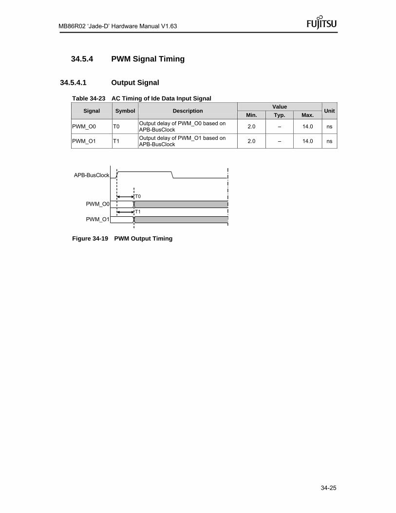
34-25
MB86R02 ‘Jade-D’ Hardware Manual V1.63
34.5.4 PWM Signal Timing
34.5.4.1 Output Signal
Table 34-23 AC Timing of Ide Data Input Signal
Signal Symbol Description Value
UnitMin. Typ. Max.
PWM_O0 T0 Output delay of PWM_O0 based on APB-BusClock
2.0 – 14.0 ns
PWM_O1 T1 Output delay of PWM_O1 based on APB-BusClock
2.0 – 14.0 ns
PWM_O0
APB-BusClock
T0
PWM_O1
T1
Figure 34-19 PWM Output Timing
34-26
MB86R02 ‘Jade-D’ Hardware Manual V1.63
34.5.5 GDC Display Signal Timing
34.5.5.1 Clock
Table 34-24 AC timing of Video Interface Clock Signal
Signal Symbol Description Value
Unit Min. Typ. Max.
DCLKP
Fdclki0 DCLKI frequency – – 67 MHz
Thdclki0 DCLKI H width 5 – – ns
Tldclki0 DCLKI L width 5 – – ns
DCLKI1
Fdclki1 DCLKI frequency – – 67 MHz
Thdclki1 DCLKI H width 5 – – ns
Tldclki1 DCLKI L width 5 – – ns
DCLK (internal) Tldclk0 DCLK frequency *1 – – 67 MHz
DCLK (internal) Tldclk1 DCLK frequency *1 – – 67 MHz
DCLKO0 Fdclko DCLKO frequency*3 – – 67 MHz
DCLKO1 Fdclko DCLKO frequency*4 – – 67 MHz
*1: Internal display clock of PLL synchronization mode is generated by division of internal PLL in the display clock prescaler. *2: DCLKI or internal display clock of PLL is output. *3: Load Capacitance 20pF *4: Load Capacitance 30pF
34.5.5.2 Input Signal
1) Apply the signal only in PLL synchronization mode (CKS = 0)
(Reference clock = Clock output from internal PLL)
Table 34-25 AC Timing of Video Interface Input Signal (1)
Signal Symbol Description Value
Unit Min. Typ. Max.
HSYNC0 (i) Twhsync0 HSYNC input pulse width 3.0 – – Clock
HSYNC1 (i) Twvsync1 VSYNC input pulse width 3.0 – – Clock
VSYNC0 (i) Twvsync VSYNC input pulse width 1 – – HSYNC
VSYNC1 (i) Twvsync VSYNC input pulse width 1 – – HSYNC
2) Apply the signal only in DCLKI synchronization mode (CKS = 1)
(Reference clock = DCLKI)
Table 34-26 AC Timing of Video Interface Input Signal (2)
Signal Symbol Description Value
Unit Min. Typ. Max.
HSYNC0 (i)
Twhsync0 HSYNC input pulse width 3.0 – – Clock
Tshsync0 HSYNC Input setup time 5.0 – – ns
Thhsync0 HSYNC Input hold time 0.0 – – ns
HSYNC1 (i)
Twhsync1 HSYNC input pulse width 3.0 – – Clock
Tshsync1 HSYNC Input setup time 5.0 – – ns
Thhsync1 HSYNC Input hold time 0.0 – – ns

34-27
MB86R02 ‘Jade-D’ Hardware Manual V1.63
VSYNC0 (i) Twvsync0 VSYNC input pulse width 1 – – HSYNC
VSYNC1 (i) Twvsync1 VSYNC input pulse width 1 – – HSYNC

34-28
MB86R02 ‘Jade-D’ Hardware Manual V1.63
34.5.5.3 Output Signal
Table 34-27 AC Timing of Video Interface Input Signal
Signal Symbol Description Value
Unit Min. Typ. Max.
DISP0[11:0]P, DISP0[11:0]N *1
Tdrgb0 RGB output delay time with “TCON bypass active”
0.2 – 6.1 ns
DOUTR1[5:0], DOUTG1[5:0], DOUTB1[5:0]
Tdrgb1 RGB output delay time -0.6 – 3.6 ns
HSYNC0 (o) *1 Tdhsync0 HSYNC output delay time, with “TCON bypass active”
1.0 – 6.0 ns
HSYNC1 (o) Tdhsync1 HSYNC output delay time -0.6 – 3.6 ns
VSYNC0 (o) *1 Tdvsync0 VSYNC output delay time, with “TCON bypass active”
1.0 – 6.0 ns
VSYNC1 (o) Tdvsync1 VSYNC output delay time -0.6 – 3.6 ns
DE0/CSYNC0 *1 Tdcsync0 CSYNC output delay time, with “TCON bypass active”
1.0 – 6.0 ns
DE1/CSYNC1 Tdcsync1 CSYNC output delay time -0.6 – 3.6 ns
GV0 *1 Tdgv0 GV output delay time, with “TCON bypass active”
1.0 – 6.0 ns
GV1 Tdgv1 GV output delay time -0.6 – 3.6 Ns
Load Capacitance 20pF except *1 Note: If hold time is deficient, inverting DCLKO clock is recommended. *1 Values are valid for DISP0 IF at TCON bypass mode, Load Capacitance 30pF
Twvsyncn
DCLK In
HSYNCn (i)
Tshsyncn Thhsyncn
Thdclkin Tldclkin1/Fdclkin
VSYNCn (i)
Tsvsyncn Thvsyncn
Twhsyncn
Figure 34-20 Display Input Signal Timing

34-29
MB86R02 ‘Jade-D’ Hardware Manual V1.63
DCLKOn (inverted)
DCLKOn
HSYNCn (o)
1/Fdclkon
VSYNCn (o)
DOUTRn[5:0] DOUTGn[5:0] DOUTBn[5:0]
Tddrgbn
CSYNCn
GVn
Tdhsyncn
Tdvsyncn
Tdcsyncn
Tdgvn
Figure 34-21 Display Output Signal Timing There is no definition of AC characteristics about analog signal.

34-30
MB86R02 ‘Jade-D’ Hardware Manual V1.63
34.5.6 TCON active Display Timing DISP0 Interface
The following values are only valid if the display clock is output at pin DCLKP/N, that means ChanSel[i=0..12]=0. If the display clock is output at another pin of DISP0 Interface the timing values might slightly differ.
Signal Symbol Description Unit min max Condition RSDS operation mode DCLKP, DCLKN
f_RSCK Frequency MHz 55.5
t_RSCK period ns 18.0 C_L=30pF
DISP0[11:0]P, DISP0[11:0]N
RSSU setup time ns 2.7 C_L=30pF, Delay[i=12]=0, Delay[i=0..11]=1 RSHD hold time ns 2.9
RSSU setup time ns 2.4 C_L=30pF, Delay[i=12]=1, Delay[i=0..11]=0 RSHD hold time ns 3.2
TSG_[12:4], HSYNC0, VSYNC0, DE0, GV0
TSIGSU setup time ns 7.4 C_L=30pF, Delay[i=12]=0, Delay[i=0..11]=1; SSWITCH[i]=0 TSIGHD hold time ns 7.4
TSIGSU setup time ns 11.9 C_L=30pF, Delay[i=12]=1, Delay[i=0..11]=0; SSWITCH[i]=0 TSIGHD hold time ns 2.9
TSIGSU setup time ns 2.9 C_L=30pF, Delay[i=12]=1, Delay[i=0..11]=0; SSWITCH[i]=1 TSIGHD hold time ns 11.9
TTL operation mode DCLKP f_TTLCK Frequency MHz 55.5
t_TTLCK period ns 18.0 C_L=tbd.
DISP0[11:0]P, DISP0[11:0]N
DISPSU setup time ns 4.0
C_L=30pF, Delay[i=0..12]=0 DISPHD hold time ns 7.0 tbd
TSG_[12:4], HSYNC0, VSYNC0, DE0, GV0
TSIGSU setup time ns 5.0
C_L=130pF, SSWITCH[i=0..12]=0 TSIGHD hold time ns
7.0 tbd

34-31
MB86R02 ‘Jade-D’ Hardware Manual V1.63
Figure 34-2234-23, RSDS operation Output Timing
Figure 34-2434-25, TTL operation output timing (1)
TTLCKH TTLCKL
50%
TTLDAT (pins DISP[i])Registers DIR_Pin_ctrl[i].Delay=0
DISPHDDISPSU
Pins TSIG[i]Register Dir_SSwitch.SSwitch =0
TSIGHDTSIGSU
TTLCK (pin DISP[j])Register DIR_Pin_ctrl[j].Delay=0
Register DIR_Pin_Ctrl[j].Polarity=1
Figure 34-2634-27, TTL operation output timing (2)

34-32
MB86R02 ‘Jade-D’ Hardware Manual V1.63
34.5.7 RSDS Characteristics
Parameter Symbol Description Value
Unit Min Typ Max
Differential
voltage
amplitude
Vd
Output differential voltage amplitude
in RSDS mode
1. BOOST=1, RL=50Ω
2. BOOST=0, RL=100Ω
124 220 332.5 mV
Common
Mode Voltage Vcm
Output common voltage in RSDS
mode
1. BOOST=1, RL=50Ω
2. BOOST=0, RL=100Ω
0.9 1.14 1.41 V
Output
Current Iload
Output current amplitude in RSDS
mode, BOOST=0, RL=100Ω 1.24 2.20 3.325 mA
Output
Current Iload
Output current amplitude in RSDS
mode, BOOST=1, RL=50Ω 2.48 4.40 6.65 mA
Maximum
Output
Frequency
frsds Maximum output frequency in RSDS
mode - - 67 MHz
34.5.8 GDC Video Capture Signal Timing
34.5.8.1 Clock
Table 34-28 AC Timing of Video Capture Interface Clock Signal
Signal Symbol Description Value
Unit Min. Typ. Max.
CCLK0, CCLK1
fCCLK Capture clock frequency – – 80 MHz
tHCCLK Capture clock H width 3 – – ns
tLCCLK Capture clock L width 3 – – ns
Note: It depends on the resolution of the video source.
34.5.8.2 Input Signal
Table 34-29 AC Timing of Video Capture Interface Input Signal
Signal Symbol Description Value
Unit Min. Typ. Max.
VIN0[7:0], VIN1[7:0]
tSVI Input setup time 5 – – ns
tHVI Input hold Time 0 – – ns
RI1[7:2] tSRI Input setup time 6 – – ns
tHRI Input hold Time 1 – – ns
GI1[7:2] tSGI Input setup time 6 – – ns
tHGI Input hold Time 1 – – ns
BI1[7:2] tSBI Input setup time 6 – – ns
tHBI Input hold Time 1 – – ns

34-33
MB86R02 ‘Jade-D’ Hardware Manual V1.63
VINHSYNC0, VINHSYNC1
tSHSI Input setup time 5 – – ns
tHHSI Input hold Time 0 – – ns
VINVSYNC0, VINVSYNC1
tSVSI Input setup time 5 – – ns
tHVSI Input hold Time 0 – – ns
VINFID0, VINFID1
tSFI Input setup time 5 – – ns
tHFI Input hold Time 0 – – ns
Figure 34-28 Video Capture Clock Input Signal Timing
1/fCCLK
tLCCLK tHCCLK
CCLK0, CCLK1
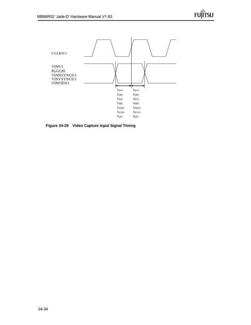
34-34
MB86R02 ‘Jade-D’ Hardware Manual V1.63
tSVI
tSRI
tSGI
tSBI
tSHSI
tSVSI
tSFI
VIN0/1
tHVI
tHRI
tHGI
tHBI
tHHSI
tHVSI
tHFI
RI,GI,BI VINHSYNC0/1 VINVSYNC0/1
CCLK0/1
VINFID0/1
Figure 34-29 Video Capture Input Signal Timing

34-35
MB86R02 ‘Jade-D’ Hardware Manual V1.63
34.5.9 I2S Signal Timing
Table 34-30 Timing Requirements
Signal Symbol Description Value
UnitMin. Typ. Max.
I2S_SCKx
tscyc Operating frequency, I2S_SCKx (slave Mode) – – 0.5B MHz
tshw Pulse duration, I2S_SCKx High (slave Mode) 0.45T – 0.55T ns
tslw Pulse duration, I2S_SCKx Low (slave Mode) 0.45T – 0.55T ns
I2S_WSx
tsfi Setup time, external I2S_WSx High before I2S_SCKx Low (slave mode)
6 – – ns
thfi Hold time, external I2S_WSx High after I2S_SCKx Low (slave Mode)
0 – – ns
I2S_SDIx
tsdi
Setup time, I2S_SDIx valid before I2S_SCKx Low (master mode)
8 TODO – – ns
Setup time, I2S_SDIx valid before I2S_SCKx Low (slave Mode)
6 – – ns
thdi
Hold time, I2S_SDIx valid after I2S_SCKx Low (master mode)
4 TODO – – ns
Hold time, I2S_SDIx valid after I2S_SCKx Low (slave mode)
0 – – ns
Table 34-31 Switching Characteristics
Signal Symbol Description Value
UnitMin. Typ. Max.
I2S_SCKx
tmcyc Operating frequency, I2S_SCKx (master mode) – – 0.5B MHz
tmhw Pulse duration, I2S_SCKx high (master mode) 0.45T – 0.55T ns
tmlw Pulse duration, I2S_SCKx low (master mode) 0.45T – 0.55T ns
I2S_WSx tdfs Delay time, I2S_SCKx High to I2S_WSx transition (master mode)
-12 – 12 ns
I2S_SDOx
tddo
Delay time, I2S_SCKx High to I2S_SDOx valid except the first bit of transmit frame. (master mode)
-12 – 17 ns
Delay time, I2S_SCKx high to I2S_SDOx valid except the first bit of transmit frame. (slave mode)
1 – 6 ns
tdfb1 Delay time, I2S_SCKx high to the first bit of a transmit frame when FSPH bit of I2Sx_CNTREG register is 1. (master mode)
-14 – 17 ns
B indicates AHB bus clock frequency. T indicates I2S_SCKx frequency.

34-36
MB86R02 ‘Jade-D’ Hardware Manual V1.63
Figure 34-30 Master Mode Timing
I2S_SCKx
I2S_WSx (FSPH=0, FSLN=0)
I2S_WSx(FSPH=1,FSLN=0)
I2S_WSx(FSPH=0, FSLN=1)
I2S_WSx(FSPH=1, FSLN=1)
I2S_SDOx
I2S_SDIx
tdfb1
tsdithd
itsdi
thd
i
tddo
tsfi thfi
tsfi thfi
tsfi
tsfi
tscyc
tshw tslw
Figure 34-31 Slave Mode Timing
FSPH is bit 2 of I2Sx_CNTREG register.
FSLN is bit 1 of I2Sx_CNTREG register.
I2S_SCKx
I2S_WSx(FSPH=0, FSLN=0)
I2S_WSx (FSPH=1, FSLN=0)
I2S_WSx(FSPH=0, FSLN=1)
I2S_WSx(FSPH=1, FSLN=1)
I2S_SDOx
I2S_SDIx
tddo
tdfstdfs
tdfstdfs
tdfs
tdfb1
tdfs
tdfs
tsdithd
itsdi
thd
i
tdfs
tmcyc
tmhw tmlw

34-37
MB86R02 ‘Jade-D’ Hardware Manual V1.63
34.5.10 UART Signal Timing
Table 34-32 AC Timing
Signal Symbol Description Value
UnitMin. Typ. Max.
UART_SOUT0 UART_SOUT1 UART_SOUT2 UART_SOUT3 UART_SOUT4 UART_SOUT5
tdo Data output delay time – – 12 ns
UART_SIN0 UART_SIN1 UART_SIN2 UART_SIN3 UART_SIN4 UART_SIN5
tdw Input data width 16A – – ns
UART_XRTS0 trtso XRTS output delay time – – 11 ns
UART_XCTS0 tctsw Input XCTS data width A – – ns
Internal clock is the standard of output delay. A indicates APB bus clock cycle, and it is different from the output delay standard clock.
Internal CLK
UART_SOUT0UART_SOUT1UART_SOUT2UART_SOUT3UART_SOUT4UART_SOUT5
UART_SIN0UART_SIN1UART_SIN2UART_SIN3UART_SIN4UART_SIN5
tdo
tdw
~~
UART_XCTS0
tctsw
trtso
UART_XRTS0
~~
Figure 34-32 UART Timing

34-38
MB86R02 ‘Jade-D’ Hardware Manual V1.63
34.5.11 I2C Bus Timing
Table 34-33 AC timing of I2C signal
Signal Symbol Description Value
Unit Min. Typ. Max.
I2C_SDA0 I2C_SDA1
TS2SDAI SDAI setup time
Normal mode 250 (*1) – – ns
High-speed mode 100 (*1) – – ns
TH2SDAI SDAI hold time
Normal mode 0.0 (*1) – – ns
High-speed mode 0.0 (*1) – – ns
TWBFI BUS free time Normal mode 4.7 (*1) – – µs
High-speed mode 1.3 (*1) – – µs
I2C_SCL0 I2C_SCL1
TCSCLI SCLI cycle time
Normal mode 1.0 (*1) – – µs
High-speed mode 2.5 (*1) – – µs
TWHSCLI SCLI H width Normal mode 4.0 (*1) – – µs
High-speed mode 0.6 (*1) – – µs
TWLSCLI SCLI L width Normal mode 4.7 (*1) – – µs
High-speed mode 1.3 (*1) – – µs
TCSCLO SCLO cycle time
Normal mode 2*m + 2 (*2) – – PCLK (*3)
High-speed mode Int (1.5*m) + 2 (*2) – – PCLK (*3)
TWHSCLO SCLO H width Normal mode m + 2 (*2) – – PCLK (*3)
High-speed mode Int (0.5*m) + 2 (*2) – – PCLK (*3)
TWLSCLO SCLO L width Normal mode m (*2) – – PCLK (*3)
High-speed mode m (*2) – – PCLK (*3)
TS2SCLI SCLI setup time
Normal mode 4.0 (*2) – – µs
High-speed mode 0.6 (*2) – – µs
TH2SCLI SCLI hold time Normal mode 4.7 (*2) – – µs
High-speed mode 1.3 (*2) – – µs
*1: I2C bus specification value *2: See I2C bus interface's clock control register (I2CxCCR) of the MB86R02 LSI product specifications for the "m" value *3: PCLK = APB bus clock cycle
I2C_SDA0(in) I2C_SDA1(in)
I2C_SDA0(out) I2C_SDA1(out)
I2C_SCL0(in) I2C_SCL1(in)
I2C_SCL0(out) I2C_SCL1(out)
D6 D7
TS2SDAI TH2SDAI TS2SCLI TH2SCLI
D4 D5 D2 D3 D0 D1 ACK
START RESTART
TWHSCLI TWLSCLI TCSCLI
D6 D7
TH2SDAO TS2SCLOTH2SCLO
D4 D5 D2 D3 D0 D1 ACK
START RESTART
TWHSCLO TWLSCLOTCSCLO
STOP
TS2SCLO
STOP
TS2SCLI TH2SCLI
TWBFI
TH2SCLO
Figure 34-33 I2C Access Timing
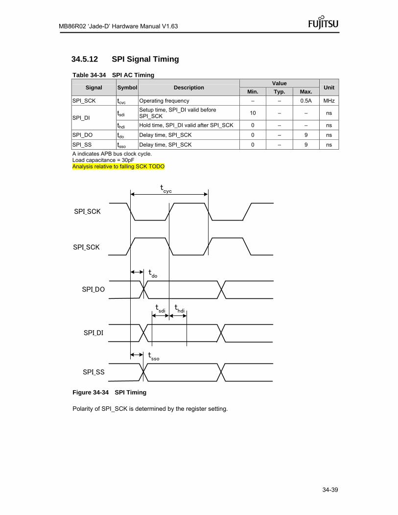
34-39
MB86R02 ‘Jade-D’ Hardware Manual V1.63
34.5.12 SPI Signal Timing
Table 34-34 SPI AC Timing
Signal Symbol Description Value
Unit Min. Typ. Max.
SPI_SCK tcyc Operating frequency – – 0.5A MHz
SPI_DI tsdi
Setup time, SPI_DI valid before SPI_SCK
10 – – ns
thdi Hold time, SPI_DI valid after SPI_SCK 0 – – ns
SPI_DO tdo Delay time, SPI_SCK 0 – 9 ns
SPI_SS tsso Delay time, SPI_SCK 0 – 9 ns
A indicates APB bus clock cycle. Load capacitance = 30pF Analysis relative to falling SCK TODO
SPI_SCK
SPI_DI
tdo
tsdi
SPI_DO
tsso
SPI_SS
thdi
SPI_SCK
tcyc
Figure 34-34 SPI Timing Polarity of SPI_SCK is determined by the register setting.

34-40
MB86R02 ‘Jade-D’ Hardware Manual V1.63
34.5.13 CAN Signal Timing
Table 34-35 CAN AC Timing
Signal Symbol Description Value
Unit Min. Typ. Max.
CAN_TX0 CAN_TX1 tdo Data output delay time – – 17 ns
CAN_RX0 CAN_RX1 tdw Input data width 1000 – – ns
Internal clock is the standard of output delay.
Internal CLK
CAN_TX0CAN_TX1
CAN_RX0CAN_RX1
tdo
tdw
~~
Figure 34-35 CAN Timing

34-41
MB86R02 ‘Jade-D’ Hardware Manual V1.63
34.5.14 MediaLB Signal Timing
34.5.14.1 MediaLB AC Spec Type A
Ground = 0V; Load capacitance = 60pF; MediaLB speed = 256Fs or 512Fs; Fs = 48kHz; all timing parameters specified from the valid voltage threshold as listed below; unless otherwise noted.
9.1.1.1.0. Clock
Table 34-36 AC Timing of Clock Signal
Signal Symbol Description Value
Unit Comment Min. Typ. Max.
MLBCLK
fmck MLBCLK operating frequency (*1)
11.264– –
– 22.5792
–
– –
24.6272 MHz
256xFs at 44.0kHz 512xFs at 44.1kHz 512xFs at 48.1kHz
tmckr MLBCLK rising time – – 3 ns VIL to VIH
tmckf MLBCLK falling time – – 3 ns VIH to VIL
tmckc MLBCLK cycle time – –
81 40
– ns 256xFs 512xFs
tmckl MLBCLK low time 30 14
37 17
– ns 256xFs 512xFs
tmckh MLBCLK high time 30 14
38 17
– ns 256xFs 512xFs
tmpwv MLBCLK pulse width variation
– – 2 ns pp
(*2)
*1: The controller can shut off MLBCLK to place MediaLB in a low-power state. *2: Pulse width variation is measured at 1.25V by triggering on one edge of MLBCLK and measuring the
spread on the other edge, measured in ns peak-to-peak (pp).
9.1.1.1.1. Input Signal
Table 34-37 AC Timing of Input Signal
Signal Symbo
l Description
Value Unit Comment
Min. Typ. Max.
MLBSIG, MLBDAT input
tdsmcf MLBSIG and MLBDAT input valid to MLBCLK falling
4 – – ns
tdhmcf MLBSIG and MLBDAT input hold from MLBCLK low
0 – – ns
Output Signal
Table 34-38 AC Timing of Output Signal
Signal Symbo
l Description
Value Unit Comment
Min. Typ. Max.
MLBSIG, MLBDAT Output
tmcfdz MLBSIG and MLBDAT output high impedance from MLBCLK low
0 – tmckl ns
tmdzh Bus hold time 4 – – ns (*1)

34-42
MB86R02 ‘Jade-D’ Hardware Manual V1.63
*1: The board must be designed to ensure that the high-impedance bus does not leave the logic state of the final driven bit for this time period. Therefore, coupling must be minimized while meeting the maximum capacitive load listed.
34.5.14.2 MediaLB AC Spec Type B
Ground = 0V, Load capacitance = 40pF, MediaLB speed = 1024Fs, and Fs = 48kHz. All timing parameters are specified from the valid voltage threshold as listed below; unless otherwise noted.
9.1.1.1.2. Clock
Table 34-39 AC Timing of Clock Signal
Signal Symbo
l Description
Value Unit
Comment Min. Typ. Max.
MLBCLK
fmck MLBCLK operating frequency (*1)
45.056– –
– 49.152
–
– –
49.2544 MHz
1024xFs at 44.0kHz1024xFs at 48.0kHz1024xFs at 48.1kHz
tmckr MLBCLK rising time – – 1 ns VIL to VIH
tmckf MLBCLK falling time – – 1 ns VIH to VIL
tmckc MLBCLK cycle time – 20.3 – ns
tmckl MLBCLK low time 6.8 7.8 – ns
tmckh MLBCLK high time 9.7 10.4 – ns
tmpwv MLBCLK pulse width variation – – 0.5 ns pp
(*2)
*1: The controller can shut off MLBCLK to place MediaLB in a low-power state. *2: Pulse width variation is measured at 1.25V by triggering on one edge of MLBCLK and measuring the spread on
the other edge, measured in ns peak-to-peak (pp).
9.1.1.1.3. Input Signal
Table 34-40 AC Timing of Input Signal
Signal Name Symbo
l Description
Value Unit Comment
Min. Typ. Max.
MLBSIG, MLBDAT input
tdsmcf MLBSIG and MLBDAT input valid to MLBCLK falling
1 – – ns
tdhmcf MLBSIG and MLBDAT input hold from MLBCLK low
0 – – ns
9.1.1.1.4. Output signal
Table 34-41 AC Timing of Output Signal
Signal Name Symbo
l Description
Value Unit Comment
Min. Typ. Max.
MLBSIG, MLBDAT Output
tmcfdz MLBSIG and MLBDAT output high impedance from MLBCLK low
0 – tmckl ns
tmdzh Bus hold time 2 – – ns (*1)
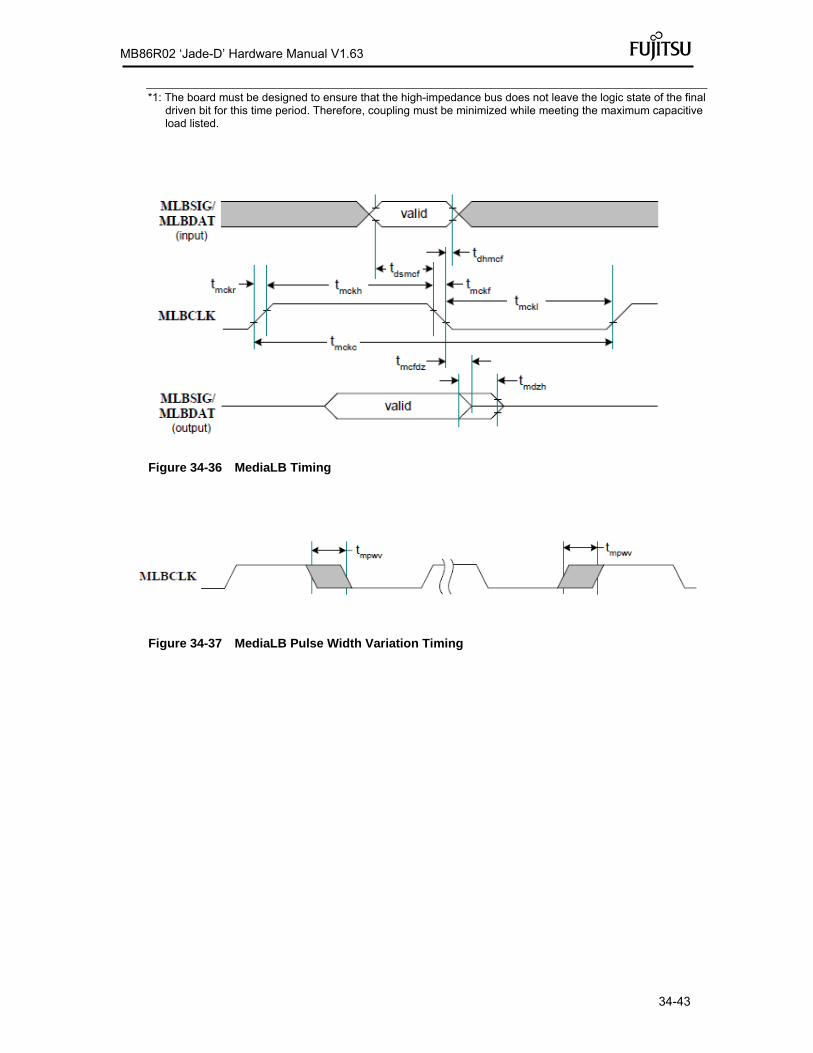
34-43
MB86R02 ‘Jade-D’ Hardware Manual V1.63
*1: The board must be designed to ensure that the high-impedance bus does not leave the logic state of the final driven bit for this time period. Therefore, coupling must be minimized while meeting the maximum capacitive load listed.
Figure 34-36 MediaLB Timing
Figure 34-37 MediaLB Pulse Width Variation Timing
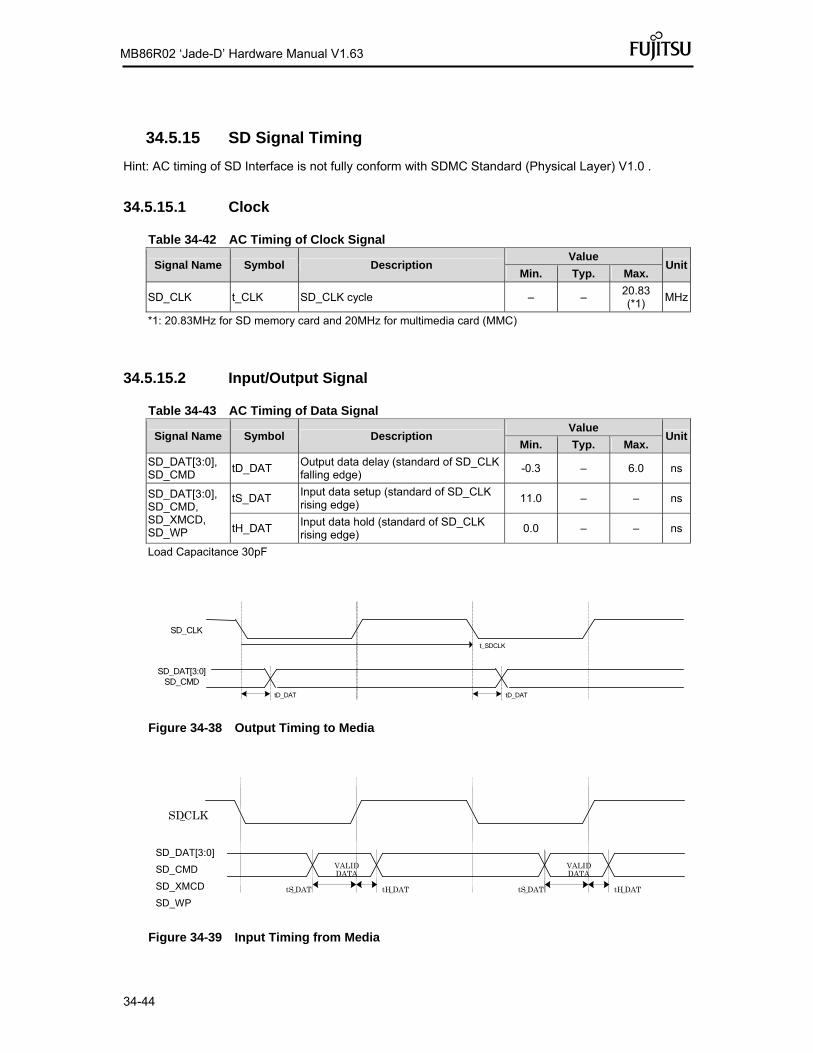
34-44
MB86R02 ‘Jade-D’ Hardware Manual V1.63
34.5.15 SD Signal Timing
Hint: AC timing of SD Interface is not fully conform with SDMC Standard (Physical Layer) V1.0 .
34.5.15.1 Clock
Table 34-42 AC Timing of Clock Signal
Signal Name Symbol Description Value
UnitMin. Typ. Max.
SD_CLK t_CLK SD_CLK cycle – – 20.83 (*1)
MHz
*1: 20.83MHz for SD memory card and 20MHz for multimedia card (MMC)
34.5.15.2 Input/Output Signal
Table 34-43 AC Timing of Data Signal
Signal Name Symbol Description Value
UnitMin. Typ. Max.
SD_DAT[3:0], SD_CMD
tD_DAT Output data delay (standard of SD_CLK falling edge)
-0.3 – 6.0 ns
SD_DAT[3:0], SD_CMD, SD_XMCD, SD_WP
tS_DAT Input data setup (standard of SD_CLK rising edge)
11.0 – – ns
tH_DAT Input data hold (standard of SD_CLK rising edge)
0.0 – – ns
Load Capacitance 30pF
SD_CLK
SD_DAT[3:0]SD_CMD
tD_DAT tD_DAT
t_SDCLK
Figure 34-38 Output Timing to Media
Figure 34-39 Input Timing from Media
SD_ DAT [3 :0 ]
SD_ CLK
VALID DATA
tS _ DAT tH_DAT
VALID DATA
tS_DAT tH _ DAT
SD_DAT[3:0]
SD_CMD
SD_XMCD
SD_WP

34-45
MB86R02 ‘Jade-D’ Hardware Manual V1.63

34-46
MB86R02 ‘Jade-D’ Hardware Manual V1.63
34.5.16 ETM9 Trace Port Signal Timing
Table 34-44 AC Timing of Trace Signal
Signal Name Symbol Description Value
UnitMin. Typ. Max.
TRACECTL
Tctlsr TRACECTL setup time to rising edge of TRACECLK.
2 – – ns
Tctlhr TRACECTL hold time to rising edge of TRACECLK. 1 – – ns
Tctlsf TRACECTL setup time to falling edge of TRACECLK.
2 – – ns
Tctlhf TRACECTL hold time to falling edge of TRACECLK. 1 – – ns
TRACEDATA[3:0]
Tdatasr TRACEDATA setup time to rising edge of TRACECLK.
2 – – ns
Tdatahr TRACEDATA hold time to rising edge of TRACECLK.
1 – – ns
Tdatasf TRACEDATA setup time to falling edge of TRACECLK.
2 – – ns
Tdatahf TRACEDATA hold time to falling edge of TRACECLK.
1 – – ns
TRACECLK
TRACECTL
Tctlsf
[NOTE] MB86R01 supports only half-rate clocking mode.
Tctlhr Tctlhf Tctlsr
Tdatasf TdatahrTdatahf Tdatasr
TRACEDATA[3:0]
Figure 34-40 Trace Signal Timing
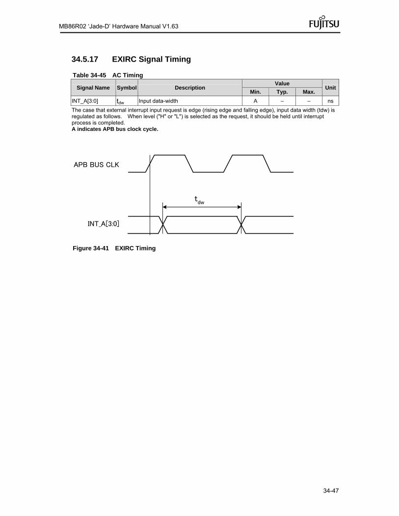
34-47
MB86R02 ‘Jade-D’ Hardware Manual V1.63
34.5.17 EXIRC Signal Timing
Table 34-45 AC Timing
Signal Name Symbol Description Value
UnitMin. Typ. Max.
INT_A[3:0] tdw Input data-width A – – ns
The case that external interrupt input request is edge (rising edge and falling edge), input data width (tdw) is regulated as follows. When level ("H" or "L") is selected as the request, it should be held until interrupt process is completed. A indicates APB bus clock cycle.
APB BUS CLK
INT_A[3:0]
tdw
Figure 34-41 EXIRC Timing

34-48
MB86R02 ‘Jade-D’ Hardware Manual V1.63
34.5.18 Apix Characteristics
34.5.18.1 Power supply
Parameter Symbol Rating
Unit Min. Typ. Max.
Power supply voltage APIXVD12 (= APIXVDD 1.2V)
1.1 1.2 1.3 V
Power supply current I APIXVD12
tbd 60 tbd mA
34.5.18.2 Transmitter Drive Current
The current that is passed onto the cable is ¼ of the drive current.
To support different types of cables and different cable lengths, the nominal drive current of the upstream transmitter is adjustable. The drive current is controlled by a digital 4 Bit Value (16 Steps). The Driver (and output) currents increase monotonically with 4-bit control value upDataSwing[3..0].
Parameter Symbol Rating Unit
Min Typ Max.
Output Current upstream for
Upstream swing upDataSwing[3..0]= 0x0
IData_Swing
3.4 4.0
4.6
mA
upDataSwing[3..0]= 0x1 3.825 4.5
5.175
upDataSwing[3..0]= 0x2
4.335 5.1
5.865
upDataSwing[3..0]= 0x3
4.76 5.6
6.44
upDataSwing[3..0]= 0x4
5.185 6.1
7.015
upDataSwing[3..0]= 0x5
5.695 6.7
7.705
upDataSwing[3..0]= 0x6
6.12 7.2
8.28
upDataSwing[3..0]= 0x7
6.545 7.7
8.855
upDataSwing[3..0]= 0x8
7.055 8.3
9.545
upDataSwing[3..0]= 0x9
7.48 8.8
10.12
upDataSwing[3..0]= 0xA
7.905 9.3
10.695

34-49
MB86R02 ‘Jade-D’ Hardware Manual V1.63
upDataSwing[3..0]= 0xB
8.415 9.9
11.385
upDataSwing[3..0]= 0xC
8.84 10.4
11.96
upDataSwing[3..0]= 0xD
9.265 10.9
12.535
upDataSwing[3..0]= 0xE
9.775 11.5
13.225
upDataSwing[3..0]= 0xF
10.2 12.0
13.8
34.5.18.3 Transmitter De-emphasis
The transmitter supports 4 levels of de-emphasis. Bits with the same value as the previous bit are transmitted with the swing reduced by the de-emphasis value. Nominal de-emphasis values are 0%, 17%, 33%, 50%.
34.5.18.4 Receiver Input Sensitivity
Parameter Symbol Rating Unit
Min. Max.
Receiver differential input swing Vdiff_pk-pk 120 1000 mV
34.5.18.5 Receiver Common Mode
Parameter Symbol Rating Unit
Min. Max.
Common mode voltage Vcm APIXVSS+0.5 APIXVD12-0.5 V
34.5.18.6 Transmitter Serial Data Signal Characteristics
The transmitter covered the total jitter requirements from APIX standard for 500Mbit/s (1000Mbit/s are still under TBD). For detailed specifications of the transmitter serial data characteristics please refer to APIX standard documentation revision 1.2 and Application Note an-mb86r02-apix-jitter-measurment-rev0-01.pdf (this is available on the technical support website for Jade-D: http://www.fujitsu.com/emea/services/microelectronics/gdc/gdcdevices/mb86r02-jade-d.html#support)

34-50
MB86R02 ‘Jade-D’ Hardware Manual V1.63
34.5.19 OSC Characteristics
34.5.19.1 Power supply
Parameter Symbol Rating
Unit Min. Typ. Max.
Power supply voltage APIXVD33 (= APIXVDD 3.3V)
3.0 3.3 3.6 V
Power supply current I APIXVD33
- 29 46 mA
34.5.19.2 Crystal and Clock buffer Frequencies
Parameter Symbol Rating
Unit Min. Typ. Max.
Crystal resonant frequency Fosc 10 25 62.5 MHz
Clock Buffer Input frequency Fclk
1 25 62.5 MHz
34.5.19.3 Internal Feedback Resistor
Parameter Symbol Rating
Unit Min. Typ. Max.
Internal Feedback Resistor Rfb 80 100 120 kΩ

35-1
MB86R02 ‘Jade-D’ Hardware Manual V1.63
35 Addendum: Differences ES1 / ES2 This section summarizes important changes that have been made between the ES1 and ES2 versions of the MB86R02 'Jade-D' devices. These are not listed in the current Errata Sheet for MB86R02 'Jade-D', which will shortly be available on the Internet at the following (new) URL: http://www.fujitsu.com/emea/services/microelectronics/gdc/gdcdevices/mb86r02-jade-d.html as they are not issues, but changes. This section does not repeat information from the Errata Sheet about known issues between ES1 and ES2 here again!
35.1 Multiplex (1)
The initial functional state of multiplex pins after a reset has changed. The differences are marked in the multiplex mode tables using */**
* Initial state for ES1
** Initial state for ES2
35.2 Multiplex (2)
The function and mode decoding of specific multiplex pins changed from ES1 to ES2. These tables show the states for the ES1/ES2 devices.
Note: The first column of each of the following tables is the default state! If a non-specified MUX function is selected then the default MUX function is applied (e.g. Pin Multiplex mode #0, '11' > first MUX function applies).
Pin multiplex mode #4
First MUX
Function
Second MUX
Function Third MUX Function Fourth MUX Function
CMPX_MODE_2[1:0] "00" */** "01" "10" "11"
Functional Group -> DISP0 DISP0 & APIX0_SB APIX0_SB & GPIOx18 GPIOx24
Pin Name: 1st Function: 2nd Function: 3rd Function: Pin Name:
DCLKP DCLKP DCLKP
ES1: Input (no function)
ES2: CONST0
ES1: Input (no function)
ES2: CONST0
DCLKN DCLKN DCLKN
ES1: Input (no function)
ES2: CONST0
ES1: Input (no function)
ES2: CONST0
VSYNC0 VSYNC0 VSYNC0 VSYNC0 VSYNC0
DE0 DE0 DE0 DE0 DE0
GV0 GV0 GV0 GV0 GV0
HSYNC0 HSYNC0 HSYNC0 HSYNC0 HSYNC0
* Initial state for ES1
** Initial state for ES2
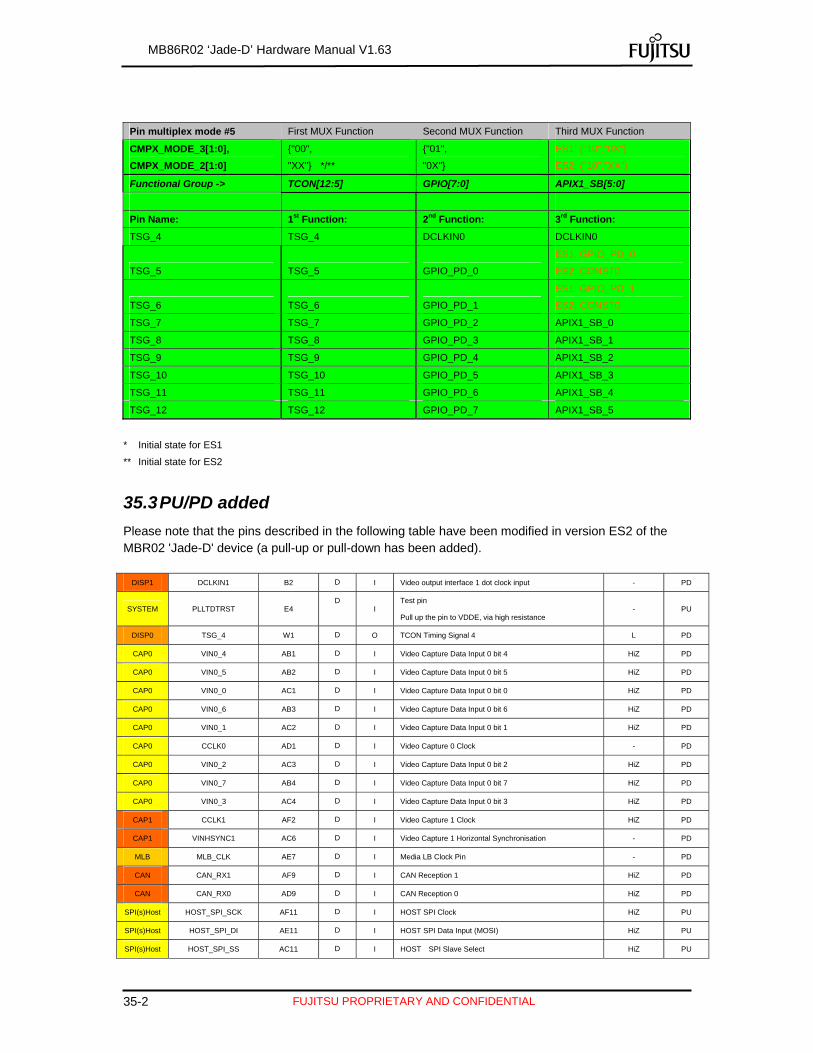
35-2
MB86R02 ‘Jade-D’ Hardware Manual V1.63
FUJITSU PROPRIETARY AND CONFIDENTIAL
Pin multiplex mode #5 First MUX Function Second MUX Function Third MUX Function
CMPX_MODE_3[1:0],
CMPX_MODE_2[1:0]
"00",
"XX" */**
"01",
"0X"
ES1: "10","0X"
ES2: "10","XX"
Functional Group -> TCON[12:5] GPIO[7:0] APIX1_SB[5:0]
Pin Name: 1st Function: 2nd Function: 3rd Function:
TSG_4 TSG_4 DCLKIN0 DCLKIN0
TSG_5 TSG_5 GPIO_PD_0
ES1: GPIO_PD_0
ES2: CONST0
TSG_6 TSG_6 GPIO_PD_1
ES1: GPIO_PD_1
ES2: CONST0
TSG_7 TSG_7 GPIO_PD_2 APIX1_SB_0
TSG_8 TSG_8 GPIO_PD_3 APIX1_SB_1
TSG_9 TSG_9 GPIO_PD_4 APIX1_SB_2
TSG_10 TSG_10 GPIO_PD_5 APIX1_SB_3
TSG_11 TSG_11 GPIO_PD_6 APIX1_SB_4
TSG_12 TSG_12 GPIO_PD_7 APIX1_SB_5
* Initial state for ES1
** Initial state for ES2
35.3 PU/PD added
Please note that the pins described in the following table have been modified in version ES2 of the MBR02 'Jade-D' device (a pull-up or pull-down has been added).
DISP1 DCLKIN1 B2 D I Video output interface 1 dot clock input - PD
SYSTEM PLLTDTRST E4 D
I Test pin
Pull up the pin to VDDE, via high resistance - PU
DISP0 TSG_4 W1 D O TCON Timing Signal 4 L PD
CAP0 VIN0_4 AB1 D I Video Capture Data Input 0 bit 4 HiZ PD
CAP0 VIN0_5 AB2 D I Video Capture Data Input 0 bit 5 HiZ PD
CAP0 VIN0_0 AC1 D I Video Capture Data Input 0 bit 0 HiZ PD
CAP0 VIN0_6 AB3 D I Video Capture Data Input 0 bit 6 HiZ PD
CAP0 VIN0_1 AC2 D I Video Capture Data Input 0 bit 1 HiZ PD
CAP0 CCLK0 AD1 D I Video Capture 0 Clock - PD
CAP0 VIN0_2 AC3 D I Video Capture Data Input 0 bit 2 HiZ PD
CAP0 VIN0_7 AB4 D I Video Capture Data Input 0 bit 7 HiZ PD
CAP0 VIN0_3 AC4 D I Video Capture Data Input 0 bit 3 HiZ PD
CAP1 CCLK1 AF2 D I Video Capture 1 Clock HiZ PD
CAP1 VINHSYNC1 AC6 D I Video Capture 1 Horizontal Synchronisation - PD
MLB MLB_CLK AE7 D I Media LB Clock Pin - PD
CAN CAN_RX1 AF9 D I CAN Reception 1 HiZ PD
CAN CAN_RX0 AD9 D I CAN Reception 0 HiZ PD
SPI(s)Host HOST_SPI_SCK AF11 D I HOST SPI Clock HiZ PU
SPI(s)Host HOST_SPI_DI AE11 D I HOST SPI Data Input (MOSI) HiZ PU
SPI(s)Host HOST_SPI_SS AC11 D I HOST SPI Slave Select HiZ PU

35-3
MB86R02 ‘Jade-D’ Hardware Manual V1.63
UART0 UART_SIN0 AF16 D I UART0 serial input 1) HiZ 2) H PD
UART2 UART_SIN2 AD17 D I UART2 serial input HiZ PD
INT INT_A_0 AF22 D I Asynchronous external interrupt requests - PD
INT INT_A_1 AE21 D I Asynchronous external interrupt requests - PD
INT INT_A_2 AD21 D I Asynchronous external interrupt requests - PD
INT INT_A_3 AC21 D I Asynchronous external interrupt requests - PD
35.4 SSCG (Spread-Spectrum Modulation)
The functional scope of the SSCG (Spread-Spectrum Modulation and Clock Generation) unit is slightly different for ES1 and ES2 versions of the MB86R02 'Jade-D':
Modulation of internal chip units and the memory clock
domain
Modulation of the display clock domain
ES1 NO YES
ES2 YES YES
35.5 Polarity of JTAGSEL
Please note that the polarity of JTAGSEL in MB86R02 'Jade-D' is different to that of MB86R01 'Jade'.
35.6 APIX Initialization
Please note that the APIX TX initialization of MB86R02 'Jade-D' is different to that of MB86R01 'Jade'.
ES1 R0CTRL(R0CFGEN) = 0
ES2 Keep reset value