MB15U36 new - Fujitsu Global 64/65 or a 128/129 for the 2.0GHz prescaler, and a 64/65 or a 128/129...
23
Fujitsu semiconductor Rev5.0 ASSP Dual Serial Input PLL Frequency Synthesizer MB15U36 DESCRIPTION The Fujitsu MB15U36 is a serial input Phase Locked Loop (PLL) frequency synthesizer with 2.0GHz and 1.2GHz prescalers. A 64/65 or a 128/129 for the 2.0GHz prescaler, and a 64/65 or a 128/129 for the 1.2GHz prescaler can be selected that enables pulse swallow operation. The latest BiCMOS process technology is used, resultantly a supply current is limited as low as 9.0mA typ. at a supply voltage of 5.0V. MB15U36 utilizes a refined charge pump design (Fujitsu’s Super Charger) that provides fast tuning along with low noise performance. MB15U36 is ideally suitable for digital mobile communications, such as CATV, PHS(Personal Handy Phone System), and PCS( Personal Communication Service). FEATURE -High frequency operation : RF synthesizer: 2.0GHz max. IF synthesizer: 1.2GHz max. -Power supply voltage : Vcc=3.0V to 5.5V -Very low power supply current : Icc=9.0mA typ. (Vcc=5.0V) -Power saving function : Ips1=Ips2=10uA max. -Serial input 15 bit programmable reference divider : R=3 to 32,767 -Serial input 18 bit programmable divider consisting of Binary 7 bit swallow counter : 0 to 127 Binary 11 bit programmable counter : 3 to 2,047 -On-chip high performance charge pump circuit and phase comparator achieved high speed settling time and low phase noise. -Wide operating temperature : Ta = -40 to +85 °C -Plastic 20 pin TSSOP package PACKAGE 20-pinPlastic SSOP FPT-20P-M03
Transcript of MB15U36 new - Fujitsu Global 64/65 or a 128/129 for the 2.0GHz prescaler, and a 64/65 or a 128/129...

Fujitsu semiconductor Rev5.0
ASSPDual Serial InputPLL Frequency Synthesizer
MB15U36
ØDESCRIPTIONThe Fujitsu MB15U36 is a serial input Phase Locked Loop (PLL) frequency synthesizer with 2.0GHz and 1.2GHzprescalers. A 64/65 or a 128/129 for the 2.0GHz prescaler, and a 64/65 or a 128/129 for the 1.2GHz prescaler canbe selected that enables pulse swallow operation.The latest BiCMOS process technology is used, resultantly a supply current is limited as low as 9.0mA typ. at asupply voltage of 5.0V. MB15U36 utilizes a refined charge pump design (Fujitsu’s Super Charger) that providesfast tuning along with low noise performance.MB15U36 is ideally suitable for digital mobile communications, such as CATV, PHS(Personal Handy PhoneSystem), and PCS( Personal Communication Service).
ØFEATURE-High frequency operation : RF synthesizer: 2.0GHz max.
IF synthesizer: 1.2GHz max.-Power supply voltage : Vcc=3.0V to 5.5V-Very low power supply current : Icc=9.0mA typ. (Vcc=5.0V)-Power saving function : Ips1=Ips2=10uA max.-Serial input 15 bit programmable reference divider : R=3 to 32,767-Serial input 18 bit programmable divider consisting of Binary 7 bit swallow counter : 0 to 127 Binary 11 bit programmable counter : 3 to 2,047-On-chip high performance charge pump circuit and phase comparator achieved high speed settling time and low phase noise.-Wide operating temperature : Ta = -40 to +85 °C-Plastic 20 pin TSSOP package
ØPACKAGE
20-pinPlastic SSOP
(FPT-20P-M06)FPT-20P-M03

Rev5.0
MB15U36
- 2 -
ØPIN ASSIGNMENT
1
2
3
4
5
6
7
8
9
10
20
19
18
17
16
15
14
13
12
11
Vcc1
Vp1
Do1
GND1
fin1
Xfin1
GND1
OSCin
OSCout
LD/fout
Vcc2
Vp2
Do2
GND2
fin2
Xfin2
GND2
LE
Data
Clock
TOPVIEW

Rev5.0
MB15U36
- 3 -
ØPIN DESCRIPTIONSPin No Pin name I/O Descriptions
1 Vcc1 − Power supply voltage input pin for the RF1-PLL section, the shift register and theoscillator input buffer. When power is OFF, latched data of RF1-PLL is cancelled.
2 Vp1 − Power supply for RF1 charge pump.(Independent of 19 pin)
3 Do1 O Charge pump output for the RF1-PLL section. Phase detector characteristics canbe reversed using the FC bit.
4 GND1 − Ground for the RF1-PLL section.
5 fin1 I Prescaler input pin for the RF1-PLL section.Connection to an external VCO should be via AC coupling.
6 Xfin1 I Prescaler complimentary input for the RF1-PLL. Section.This pin should be grounded via a capacitor.
7 GND1 − Ground for the RF1-PLL section.
8 OSCin I The programmable reference divider input. External TCXO reference oscillatorinput or connection to crystal. TCXO should be connected with via AC coupling.
9 OSCout − Oscillator output or connection to crystal.
10 LD/fout O Lock detect signal output (LD) / phase comparator monitoring output (fout).The output signal is selected by the LDS and FDS bits in the serial data.
11 Clock I Clock input for the 22 bit shift register.One bit data is shifted into the shift register on a rising edge of the clock.
12 Data ISerial data input. Data is transferred to the corresponding latch (RF1-ref counter,RF1-prog counter, RF2-ref counter, RF2-prog counter according to the controlbits setting in the serial programming data.
13 LE ILoad enable signal input.When LE is “H”, data in the shift register is transferred to the corresponding latchaccording to the control bits in the serial programming data.
14 GND2 − Ground for the RF2-PLL section.
15 Xfin2 I Prescaler complimentary input for the RF2-PLL section.This pin should be grounded via a capacitor.
16 fin2 I Prescaler input pin for the RF2-PLL section.Connection to an external VCO should be via AC coupling.
17 GND2 − Ground for the RF2-PLL section.
18 Do2 O Charge pump output for the RF2-PLL section. Phase detector characteristics canbe reserved using FC bit.
19 Vp2 − Power supply voltage for the RF2 charge pump.(Independent of 2 pin)
20 Vcc2 − Power supply voltage input pin for the RF2-PLL section. When power is OFF,latched data of IF-PLL is cancelled.

Rev5.0
MB15U36
- 4 -
ØBLOCK DIAGRAM PKG:TSSOP-20(FPT-20-M03)
fin1
Xfin2
2bit latch
SWRF2PSRF2
7-bit latch 11-bit latchBinary 7-bit
swallow counter(RF2-PLL)
Binary 11-bitProgrammable counter
(RF2-PLL)
Vcc2 GND2
fpRF2 Phase comp(RF2-PLL)
Charge comp(RF2-PLL) DO2
Lock det.(RF2-PLL)
frRF2
5-bit latch 15-bit latchFC RF2
Binary 15-bitProgrammable ref.counter (RF2-PLL)
5-bit latch 15-bit latch
Binary 15-bitProgrammable ref.counter (RF1-PLL)
Selector
LDRF2
LDRF1
f rRF2
f rRF1
fpRF2
fpRF1
Vcc1
LDRF2
Lock det.(RF1-PLL)
LDRF1
Phase comp(RF1-PLL)
Charge pump(RF1-PLL)
frRF1
2bit latch
SWRF1PSRF1
7-bit latch 11-bit latch
Binary 7-bitswallow counter
(RF1-PLL)
Binary 11-bitProgrammable counter
(RF1-PLL)
OSCin
OR
Rrescaler(RF-PLL)
64/65,128/129
fin1
Xfin1
LE Latch selector
DataClock
CN1 22-bit shift register
fpRF1
GND1
LD/fout
Do1
CN2
Prescaler(RF2-PLL)
64/65,128/129
20 14 17
18
10
3
7 4 1
11
12
13
6 5
8
15 16
CMC RF2
ZC RF2
LDS RF2
FDS RF2
FC RF1
CMC RF1
ZC RF1
LDS RF1
FDS RF1
9OSCout
2
Vp1
19Vp2

Rev5.0
MB15U36
- 5 -
ØABSOLUTE MAXIMUM
Parameter Symbol Rating Unit Remark
Vcc -0.5 to 6.5 VPower supply voltage
Vp -0.5 to 6.5 V
Input voltage Vi -0.5 to 6.5 V
Output voltage Vo -0.5 to 6.5 V
Storage temperature TSTG -55 to +125 °C
Note: Permanent device damage may occur if the above Absolute Maximum Ratings areexceeded. Functional operation should be restricted to the conditions as detailed inthe operational sections of this data sheet. Exposure to absolute maximum rating conditions for extendedperiods may affect device reliability.
ØRECOMMENDED OPERATING CONDITIONS
ValueParameter Symbol
Min. Typ. Max.Unit Remark
4.5 5.0 5.5 V Vcc1=Vcc2Vcc
3.0 5.5 5.5 V Vcc1=Vcc2 *1Power supply voltage
Vp Vcc - 5.5 V
Input voltage Vi GND - Vcc V
Operating temperature Ta -40 - +85 °C
*1:Prescaler divide ratio is only 64/65 (SW=”L”) at RF1
Handling Precautions-This device should be transported and stored in anti-static containers.-This is a static-sensitive device ; take proper anti-ESD precautions. Ensure that personneland equipment are properly grounded. Cover workbenches with grounded conductive mats.
-Always turn the power supply off before inserting or removing the device from its socket.-Protect leads with a conductive sheet when handling or transporting PC boards with devices

Rev5.0
MB15U36
- 6 -
ØELECTRICAL CHARACTERISITCS
Parameter Symbol Condition Value Unit
Vcc=5.0V − 6.0 − mAIcc1*1 fin1=2000MHz
fosc=12MHz Vcc=3.0V − 3.5 − mA
Vcc=5.0V − 3.0 − mAPower supply current
Icc2*2 fin2=1200MHzfosc=12MHz Vcc=3.0V − 2.5 − mA
Ips1 Vcc1 current at PsbitRF1/RF2=”H” − 0.1*3 10 uAPower saving current
Ips2 Vcc2 current at PsbitRF2=”H” − 0.1*3 10 uA
fin1*4 RF1-PLL 100 − 2000 MHz
fin2*4 RF2-PLL 50 − 1200 MHzOperating frequency
fosc Min. 500mVpp 3 − 40 MHz
RF1-PLL, 50Ω termination -10 − +2 dBm
Pfin1 RF1-PLL, Vcc=3.5V300MHz<fin<1000MHz50Ω term ination
-18 − +2 dBm
Pfin2 RF2-PLL, 50Ω termination -10 − +2 dBm
Input sensitivity
Vosc 500 − Vcc mVp-p
VIH Vcc×0.8 − − VInput voltage
Data,ClockLE VIL − − Vcc×0.2 V
IIH*5 VIH=Vcc -1.0 − +1.0 uAData,ClockLE IIL*5 VIH=0Vcc -1.0 − +1.0 uA
IIH VIH=Vcc 0 − +100 uAInput current
OSCinIIL*5 VIH=0Vcc -100 − 0 uA
VOH IOH=-1mA Vcc-0.4 − − VLD/fout
VOL IOL=1mA − − 0.4 V
VDOH IDOH=-0.5mA Vp-0.4 − − nAOutput voltage
Do1Do2
VDOL IDOL=0.5mA − − 0.4 mA
High impedancecutoff current
Do1Do2 IOFF
Vcc=Vp=5.0V0.5V≤VDO≤Vp-0.5V − − 3.0 nA
IOH*5 Vcc=5.0V − − -1.0 mAOutput current LD/fout
IOL Vcc=5.0V +1.0 − − mA

Rev5.0
MB15U36
- 7 -
ØELECTRICAL CHARACTERISITCS (Continued)
ValueParameter Symbol Condition
MIN TYP MAXUnit
Vcc=Vp=5.0V,VDOH=Vp/2CMCbit=”L”,Ta=25°C − -1.25 − mA
IDOH*5Vcc=Vp=3.0V,VDOH=Vp/2CMCbit=”L”,Ta=25°C − -1.00 − mA
Vcc=Vp=5.0V,VDOL=Vp/2CMCbit=”L”,Ta=25°C − 1.25 − mA
IDOL Vcc=Vp=3.0V,VDOL=Vp/2CMCbit=”L”,Ta=25°C − 1.00 − mA
Vcc=Vp=5.0V,VDOH=Vp/2CMCbit=”H”,Ta=25°C − -5.00 − mA
IDOH*5Vcc=Vp=3.0V,VDOH=Vp/2CMCbit=”H”,Ta=25°C − -4.00 − mA
Vcc=Vp=5.0V,VDOH=Vp/2CMCbit=”H”,Ta=25°C − 5.00 − mA
Outputcurrent
Do1
Do2
IDOL Vcc=Vp=3.0V,VDOH=Vp/2CMCbit=”H”,Ta=25°C − 4.00 − mA
IDOL/IDOH IDOMT*6 VDO=Vp/2,Ta=25°C − 3 − %
IDO vs VDO IDOVD*7 0.5V≤VDO≤Vp-0.5VTa=25°C
− 15 − %
Cp currentchangeratio
IDO vs Ta IDOTA*8 VDO=Vp/2-40°C ≤Ta≤+85°C
− 10 − %
∗1:Conditions: Vcc1=5.0V, Ta=25°C in locking state∗2:Conditions: Vcc2=5.0V, Ta=25°C in locking state∗3:Conditions: Vcc=5.0V, Ta=25°C, fosc=12.8MHz(-2dBm)∗4:AC coupling. The minimum frequency is specified with a connecting coupling capacitor of 1000pF. Please note the harmonics when using at the low frequency(<1/2 max.frequency)∗5:The symbol “-“ means direction of current flow.∗6:Conditions: Vcc=Vp=5.0V, Ta=25°C ( | | I3 | - | I4 | | )/ [( | I3 | + | I4 | )/2] × 100%∗7:Conditions: Vcc=Vp=5.0V, Ta=25°C [( | | I2 | - | I1 | | ) /2] /[( | I1 | + | I2 | )/2] × 100% (Applied to each IDOL,IDOH)∗8:Conditions: Vcc=Vp=5.0V [( | | IDO(85°c) | - | IDO(-40°c) | | ) /2] /[( | I DO(85°c) | + | I DO(-40°c) | )/2] × 100%(Applied to each IDOL,IDOH)
CP output voltage(V)
0.5V Vp/2 Vp-0.5V
I3 I2I1
I1I4I2
IDOL
IDOH

Rev5.0
MB15U36
- 8 -
Ø FUNCTIONAL DESCRIPTION
The divide ratio can be calculated using the following equation:fvco = [ ( P × N ) + A ] × fosc / R (A<N)fvco : Output frequency of external voltage controlled oscillator (VCO)P : Preset divide ratio of dual modulus prescaler (64 or 128 for RF1-PLL or RF2-PLL)N : Preset divide ratio of binary 11-bit programmable counter (3 to 2,047)A : Preset divide ratio of binary 7-bit swallow counter (0≤A≤127)fosc: Output frequency of the reference frequency oscillatorR : Preset divide ratio of binary 15-bit programmable reference counter (3 to 32,767)
Serial Data Input
Serial data is entered using three pins, Data pin, Clock pin, and LE pin. Programmable dividers ofRF1/RF2-PLL sections, programmable reference dividers of IF/RF-PLL sections are controlled individually.Serial data of binary data is entered through Data pin.On rising edge of clock, one bit of serial data is transferred into the shift register. When load enablesignal is high, the data stored in the shift register is transferred to one of latch them depending uponthe control bit data setting.
Table1. control Bit
Control bit
CN1 CN2Destination of serial data
L L The programmable reference counter for the RF2-PLL
L H The programmable reference counter for the RF1-PLL
H L The programmable counter and the swallow counter for the RF2-PLL
H H The programmable counter and the swallow counter for the RF1-PLL

Rev5.0
MB15U36
- 9 -
Shift Register Configuration
Programmable Reference Counter
LSB Data Flow MSB
1 2 3 4 5 6 7 8 9 10 11 12 13 14 15 16 17 18 19 20 21 22
CN1
CN2
R1
R2
R3
R4
R5
R6
R7
R8
R9
R10
R11
R12
R13
R14
R15
FC
CMC
ZC
LDS
FDS
CN1,2 :Control bitR1 to R15 :Divide ratio setting bits for the programmable reference counter(3 to 32,767)FC :Phase control bit for the phase detectorCMC :Charge pump output current control bitZC :Forced high-impedance control bit for the charge pumpLDS/FDS :LD/fout signal select bitNote: Start data input with MSB first
Programmable Counter
LSB Data Flow MSB
1 2 3 4 5 6 7 8 9 10 11 12 13 14 15 16 17 18 19 20 21 22
CN1
CN2
A1
A2
A3
A4
A5
A6
A7
N1
N2
N3
N4
N5
N6
N7
N8
N9
N10
N11
SW
PS
CN1 :Control bitN1 to N11 :Divide ratio setting bits for the programmable counter(3 to 2,047)A1 to A7 :Divide ratio setting bits for the swallow counter(0 to 127)SW :Divide ratio setting bit for the prescaler
(64/65 or 128/129 for the RF1/RF2-PLL)PS :Power saving mode control bitNote: Start data input with MSB first
Rev5.0
MB15U36
- 10 -
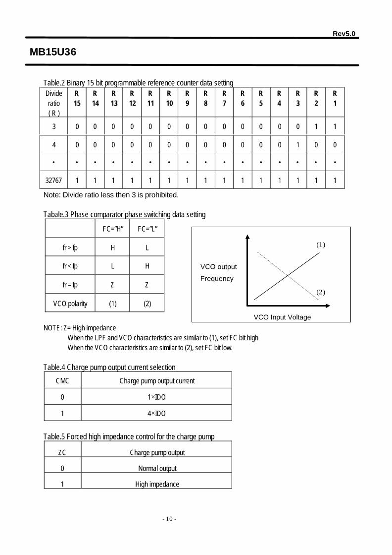
Table.2 Binary 15 bit programmable reference counter data settingDivideratio( R )
R15
R14
R13
R12
R11
R10
R9
R8
R7
R6
R5
R4
R3
R2
R1
3 0 0 0 0 0 0 0 0 0 0 0 0 0 1 1
4 0 0 0 0 0 0 0 0 0 0 0 0 1 0 0
• • • • • • • • • • • • • • • •
32767 1 1 1 1 1 1 1 1 1 1 1 1 1 1 1
Note: Divide ratio less then 3 is prohibited.
Tabale.3 Phase comparator phase switching data setting
FC=”H” FC=”L”
fr > fp H L
fr < fp L H
fr = fp Z Z
VCO polarity (1) (2)
NOTE: Z= High impedanceWhen the LPF and VCO characteristics are similar to (1), set FC bit highWhen the VCO characteristics are similar to (2), set FC bit low.
Table.4 Charge pump output current selection
CMC Charge pump output current
0 1×IDO
1 4×IDO
Table.5 Forced high impedance control for the charge pump
ZC Charge pump output
0 Normal output
1 High impedance
VCO Input Voltage
VCO output
Frequency
(1)
(2)

Rev5.0
MB15U36
- 11 -
Table.6 LD/fout output select data setting
LDSRF LDSIF RDSRF RDSIF LD/fout output signal
0 0 0 0 Disabled
0 1 0 0 LD signal (RF2 lock detect)
1 0 0 0 LD signal (RF1 lock detect)
1 1 0 0 LD signal (RF1/RF2 lock detecy)
× 0 0 1 fout (output frRF2)
× 0 1 0 fout (output frRF1)
× 1 0 1 fout (output fpRF2)
× 1 1 0 fout (output fpRF1)
0 0 1 1 Fast lock
0 1 1 1 RF2 counter reset
1 0 1 1 RF1 counter reset
1 1 1 1 RF1/RF2 Counter reset
Note : ×=don’t careThe Fast lock mode utilizes the LD/fout output pin. While Fast lock mode, whenever RFCharge pump output current select bit(CMCRF bit) is selected “H”, LD/fout output pin(open drain output) is “L”. When CMCRF bit is selected”L”, LD/fout output pin(open drain
output) is “Z”.(See Fast lock circuit example)
Table.7 Binary 11 bit Programmable counter data settingDivideratio( N )
N11
N10
N9
N8
N7
N6
N5
N4
N3
N2
N1
3 0 0 0 0 0 0 0 0 0 1 1
4 0 0 0 0 0 0 0 0 1 0 0
• • • • • • • • • • • •
2047 1 1 1 1 1 1 1 1 1 1 1
Note: Divide ratio less than 3 is prohibited.
Rev5.0
MB15U36
- 12 -
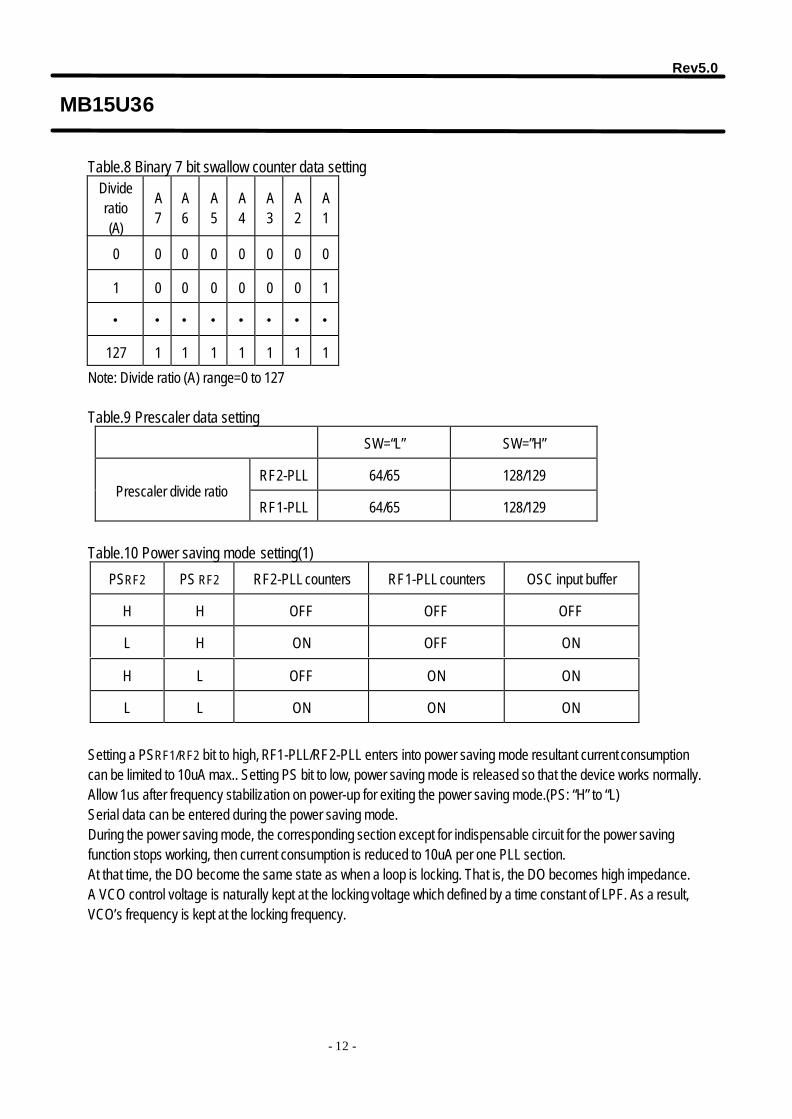
Table.8 Binary 7 bit swallow counter data settingDivideratio(A)
A7
A6
A5
A4
A3
A2
A1
0 0 0 0 0 0 0 0
1 0 0 0 0 0 0 1
• • • • • • • •
127 1 1 1 1 1 1 1
Note: Divide ratio (A) range=0 to 127
Table.9 Prescaler data setting
SW=“L” SW=”H”
RF2-PLL 64/65 128/129Prescaler divide ratio
RF1-PLL 64/65 128/129
Table.10 Power saving mode setting(1)
PSRF2 PS RF2 RF2-PLL counters RF1-PLL counters OSC input buffer
H H OFF OFF OFF
L H ON OFF ON
H L OFF ON ON
L L ON ON ON
Setting a PSRF1/RF2 bit to high, RF1-PLL/RF2-PLL enters into power saving mode resultant current consumptioncan be limited to 10uA max.. Setting PS bit to low, power saving mode is released so that the device works normally.Allow 1us after frequency stabilization on power-up for exiting the power saving mode.(PS: “H” to “L)Serial data can be entered during the power saving mode.During the power saving mode, the corresponding section except for indispensable circuit for the power savingfunction stops working, then current consumption is reduced to 10uA per one PLL section.At that time, the DO become the same state as when a loop is locking. That is, the DO becomes high impedance.A VCO control voltage is naturally kept at the locking voltage which defined by a time constant of LPF. As a result,VCO’s frequency is kept at the locking frequency.

Rev5.0
MB15U36
- 13 -
Serial data input timing
Table11.Timing parametersParameter MIN. TYP. MAX. Unit Note
t0 100 − − ns CK Rate
t1 20 − − ns tsu CK → Data
t2 20 − − ns th CK → Data
t3 30 − − ns tsu LE
t4 20 − − ns tsu inactive
t5 30 − − ns tw CK
t6 100 − − ns tw LE
On rising edge of the clock, one bit of the data is transferred into the shift register.
t0 t1t2
t5
t3
t6
t4
MSB LSBData
Clock
LE

Rev5.0
MB15U36
- 14 -
Ø Phase detector output waveform
Note: Phase error detection range = -2π to +2πPulse on DoRF1/RF2 signals are output to prevent dead zone.
LD
frRF1/RF2
fpRF1/RF2
Z
ZDoRF1/RF2
DoRF1/RF2
(FC bit=“H”)
(FC bit=“L”)

Rev5.0
MB15U36
- 15 -
Ø TEST CIRCUIT(Prescaler Input/Programmable Reference Divider Input Sensitivity Test)
10 9 8 7 6 5 4 3 2 1
11 12 13 14 15 16 17 18 19 20
Vp1 Vcc1Do1GND1fin1Xfin1GND1OSCIOSCoutLD/fout
Vp2 Vcc2Do2GND2fin2Xfin2GND2LEDataClock
0.1µ
Vcc1
1000pF
1000pF
50Ω S.G
Oscilloscopefout
1000pF
50Ω
S.G
50Ω
S.G1000pF
10001000pF0.1µ 0.1µ
Vcc2
Controller(divide ratio setting)

Rev5.0
MB15U36
- 16 -
Ø TYPICAL CHARACTERISTICS1.fin input sensitivity
2.OSCin Input seinsitivity
-50
-40
-30
-20
-10
0
10
0 500 1000 1500 2000
finRF2 [MHz]
Vfin
RF2
[dBm
]
Vfin[dBm]@5.5V
Vfin[dBm]@5.0V
Vfin[dBm]@4.5V
Vfin[dBm]@3.0V
SPEC
-50
-40
-30
-20
-10
0
10
0 500 1000 1500 2000 2500 3000
finRF1 [MHz]
Vfin
RF1
[dBm
]
Vfin[dBm]@5.5V
Vfin[dBm]@5.0V
Vfin[dBm]@4.5V
Vfin[dBm]@3.0V
SPEC
at Vcc=3.5V
Input sensitivity of fin (RF1) versus Input frequency
Input sensitivity of fin (RF2) versus Input frequency
-50
-40
-30
-20
-10
0
10
0 50 100 150 200 250
fosc [MHz]
VOSC
[dBm
]
VOSCin[dBm]@5.5V
VOSCin[dBm]@5.0VVOSCin[dBm]@4.5VVOSCin[dBm]@3.0V
SEPC

Rev5.0
MB15U36
- 17 -
3.Do output current (1×Do mode)
IDOH VS. VDOH
0
1
2
3
4
5
6
7
8
-3-2.5-2-1.5-1-0.50
Vcc=5VVcc=3V
“H” level output voltage IDOH (mA)
“H” l
evel
out
put v
olta
ge V
DOH
(V)
IDOL VS. VDOL
0
1
2
3
4
5
6
7
8
0 0.5 1 1.5 2 2.5 3
Vcc=5VVcc=3V
“L” level output current IDOL(mA)
“L” l
evel
out
put v
olta
ge V
DOL
(V)

Rev5.0
MB15U36
- 18 -
4.Do output current (4×Do mode)
IDOH VS. VDOH
0
1
2
3
4
5
6
7
8
-8-7-6-5-4-3-2-10
Vcc=5VVcc=3V
“H” level output voltage IDOH (mA)
"H” l
evel
out
put v
olta
ge V
DO
H (V
)
IDOL VS. VDOL
0
1
2
3
4
5
6
7
8
0 1 2 3 4 5 6 7 8
Vcc=5VVcc=3V
“L” level output voltage IDOL (mA)
“L” l
evel
out
put v
olta
ge V
DOL
(V)

Rev5.0
MB15U36
- 19 -
5.Input impedance
Input impedance of fin (RF1)
Input impedance of fin (RF2)

Rev5.0
MB15U36
- 20 -
5.Input impedance
Input impedance of fin (OSCin)

Rev5.0
MB15U36
- 21 -
Ø APPLICATION EXAMPLE
Clock, Data, LE : Insert a pull-down or pull-up resister as needed to prevent oscillation when the terminals
are left open.
10987654321
11121314151617181920
Vp1Vcc1 Do1 GND1 fin1 Xfin1 GND1 OSCIN OSCout LD/fout
Vp2Vcc2 Do2 GND2 fin2 Xfin2 GND2 LE Data Clock
1000pF From Controller
Output
1000pF0.1µ 0.1µ
1000pF
LPF VCO
LPF VCO
TCXO
Output
0.1µ
0.1µ
MB15U36
1000pF

Rev5.0
MB15U36
- 22 -
Ø APPLICATION EXAMPLE : Fast lock mode
Clock, Data, LE : Insert a pull-down or pull-up resister as needed to prevent oscillation when the terminals
are left open.
The Fastlock mode is controlled by the LDS/FDS bits and the CMCRF1 bit. When the CMCRF1 bit is set to“H” (the RF1 charge pump current is increased 4x normal mode), the LD/fout pin (open drain output) is “L”,enabling the parallel resistor in the loop filter. This effectively increases the LPF bandwidth, allowing theloop to lock faster. After the loop has locked onto a new frequency, the CMC RF1 bit is set to “L”, forcing theLD/fout output pin into a high impedance state and returning the LPF bandwidth back to its original value.
10987654321
11121314151617181920
Vp1Vcc1 Do1 GND1 fin1 Xfin1 GND1 OSCIN OSCout LD/fout
Vp2Vcc2 Do2 GND2 fin2 Xfin2 GND2 LE Data Clock
1000pF From Controller
Output
1000pF0.1µ 0.1µ
1000pF
LPF
VCO
LPF VCO
TCXO
Output
0.1µ0.1µ
MB15U36

Rev5.0
MB15U36
- 23 -
Ø PACKAGE DIMENSION
Ø ORDERING INFORMATION
Part number Package Remarks
MB15U36PFV 20pin Plastic SSOP(FPT-20P-M03) -
20pins, Plastic SSOP(FPT-20P-M03)

![Chausseestraße 128/129 — 10115 Berlin — +49 /21 /22 /fax ... · neuer.berliner.kunstverein. e.V. Chausseestraße 128/129 — 10115 Berlin — +49 [0]30 280 70 20 /21 /22 /fax](https://static.fdocuments.us/doc/165x107/5fab6ace30e78868944c5d8e/chausseestrae-128129-a-10115-berlin-a-49-21-22-fax-neuerberlinerkunstverein.jpg)


![Index [assets.cambridge.org]assets.cambridge.org/97805218/45120/index/... · Index 301 National Socialist Archives, housing in, 129 Scheubner-Richter, Max, editor of, 128–129 Schickedanz,](https://static.fdocuments.us/doc/165x107/5f37b8c6c59f5d20575125a2/index-index-301-national-socialist-archives-housing-in-129-scheubner-richter.jpg)