
MAX30110 ptimie lse-imeter an Heart ate A orearale Healt · MAX30110 Optimized Pulse-Oximeter and...
37
General Description The MAX30110 is a complete optical pulse oximetry and heart rate detection integrated analog front-end. The MAX30110 has a high-resolution, optical readout signal- processing channel with built-in ambient light cancellation, as well as high-current LED driver DACs, to form a complete optical readout signal chain. With external LED(s) and photo diode(s), the MAX30110 offers the lowest power, highest performance heart rate detection solution for wrist applications. The MAX30110 operates on a 1.8V main supply voltage, with a separate 3.1V to 5.25V LED driver power supply. The device supports a standard SPI compatible interface, as well as shutdown modes through the software with near-zero standby current, allowing the power rails to remain powered at all times. Applications ● Wrist-Worn Wearable Devices ● In-Ear Wearable Devices ● SpO 2 Monitoring Devices ● Fitness Wearable Devices Benefits and Features ● Reflective or Transmissive Heart Rate, Heart Rate Variability, or SpO 2 Monitoring ● Transmit Section • Two 8-bit LED Current DACs • Four Current Ranges 50mA, 100mA, 150mA, 200mA • Low Noise Current Sources for High Peak Transmit to Receive Dynamic Range • Low 160mV Dropout to Support Direct Drive From Rechargeable Li Battery • High Output Impedance and High Supply Rejection to Support Unregulated Supply or Direct Drive From Boost Switcher Supply Ordering Information appears at end of data sheet. 19-100092; Rev 0; 6/17 ● Receive Section • 19-bit Optical ADC Path to Support the Lowest Perfusions Situations • Low 25pA-RMS Input Referred Noise to Minimize LED Power Under Most Conditions • High Ambient Light Input Range of 200μA and to Support Extraction of HRM Signal in the Most Adverse Lighting Conditions • Built-in Front And Back-End Ambient Light Cancellation, Improving Rejection and Eliminating System Complexity of Dealing with Ambient Light • Short Exposure Pulse Widths of 52μs, 104μs, 206μs, 417μs for Efficient Uses of LED Light • Multiple Sample Rate Options from 20sps to 3.2ksps ● Ultra-Low-Power Operation for Mobile and Body- Wearable Device • Dynamic Power-Down Modes to 100sps for Low-Power Consumption • Full AFE Power Consumption of Less Than 25μA (Typ) at 25sps • Large 32 Sample FIFO to Support Batch Processing in the Microcontroller • Variety of System Monitors Mappable to Interrupts to Off-Load System Monitoring Functions From the Microcontroller • Low Shutdown Current = 1.4μA (typ) ● SPI Interface ● Supports a Single 1.8V Supply with Separate 3.1V to 5.25V LED Supply ● Miniature 2.8mm x 2.0mm, 6x4, 0.4mm Ball Pitch WLP Package ● -40°C to +85°C Operating Temperature Range MAX30110 Optimized Pulse-Oximeter and Heart Rate AFE forWearable Health EVALUATION KIT AVAILABLE
Transcript of MAX30110 ptimie lse-imeter an Heart ate A orearale Healt · MAX30110 Optimized Pulse-Oximeter and...

General DescriptionThe MAX30110 is a complete optical pulse oximetry and heart rate detection integrated analog front-end. The MAX30110 has a high-resolution, optical readout signal-processing channel with built-in ambient light cancellation, as well as high-current LED driver DACs, to form a complete optical readout signal chain. With external LED(s) and photo diode(s), the MAX30110 offers the lowest power, highest performance heart rate detection solution for wrist applications.The MAX30110 operates on a 1.8V main supply voltage, with a separate 3.1V to 5.25V LED driver power supply. The device supports a standard SPI compatible interface, as well as shutdown modes through the software with near-zero standby current, allowing the power rails to remain powered at all times.
Applications ● Wrist-Worn Wearable Devices ● In-Ear Wearable Devices ● SpO2 Monitoring Devices ● Fitness Wearable Devices
Benefits and Features ● Reflective or Transmissive Heart Rate, Heart Rate
Variability, or SpO2 Monitoring ● Transmit Section
• Two 8-bit LED Current DACs• Four Current Ranges 50mA, 100mA, 150mA, 200mA• Low Noise Current Sources for High Peak Transmit
to Receive Dynamic Range• Low 160mV Dropout to Support Direct Drive From
Rechargeable Li Battery• High Output Impedance and High Supply Rejection
to Support Unregulated Supply or Direct Drive From Boost Switcher Supply
Ordering Information appears at end of data sheet.
19-100092; Rev 0; 6/17
● Receive Section• 19-bit Optical ADC Path to Support the Lowest
Perfusions Situations• Low 25pA-RMS Input Referred Noise to Minimize
LED Power Under Most Conditions• High Ambient Light Input Range of 200μA and
to Support Extraction of HRM Signal in the Most Adverse Lighting Conditions
• Built-in Front And Back-End Ambient Light Cancellation, Improving Rejection and Eliminating System Complexity of Dealing with Ambient Light
• Short Exposure Pulse Widths of 52μs, 104μs, 206μs, 417μs for Efficient Uses of LED Light
• Multiple Sample Rate Options from 20sps to 3.2ksps
● Ultra-Low-Power Operation for Mobile and Body-Wearable Device• Dynamic Power-Down Modes to 100sps for
Low-Power Consumption• Full AFE Power Consumption of Less Than 25μA
(Typ) at 25sps• Large 32 Sample FIFO to Support Batch Processing
in the Microcontroller• Variety of System Monitors Mappable to Interrupts
to Off-Load System Monitoring Functions From the Microcontroller
• Low Shutdown Current = 1.4μA (typ) ● SPI Interface ● Supports a Single 1.8V Supply with Separate 3.1V to
5.25V LED Supply ● Miniature 2.8mm x 2.0mm, 6x4, 0.4mm Ball Pitch
WLP Package ● -40°C to +85°C Operating Temperature Range
MAX30110 Optimized Pulse-Oximeter and Heart Rate AFE forWearable Health
EVALUATION KIT AVAILABLE

Simplified Block Diagram
GND_ANA GND_DIG
VLED
PD_GND
PD_IN
LED1_DRV
LED2_DRV
C2_P
SDO
CSB
INT
VDD_ANA
PGND
19-BIT CURRENT ADC
AMBIENT CANCELLATION
DIGITAL NOISE CANCELLATION
32 SAMPLE FIFO
LED DRIVERS
SPI I
NTE
RFA
CE
REFERENCE
MAX30110
VDD_DIG
SCLK
SDI
FCLK
www.maximintegrated.com Maxim Integrated │ 2
MAX30110 Optimized Pulse-Oximeter and Heart Rate AFE for Wearable Health

VDD_ANA to GND_ANA ......................................-0.3V to +2.2VVDD_DIG to GND_ANA .......................................-0.3V to +2.2VVDD_ANA to VDD_DIG........................................-0.3V to +0.3VPGND to GND_ANA .............................................-0.3V to +0.3VGND_DIG to GND_ANA .......................................-0.3V to +0.3VVLED to PGND.....................................................-0.3V to +6.0VLED1_DRV to PGND ................................ -0.3V to VLED + 0.3VLED2_DRV to PGND ................................ -0.3V to VLED + 0.3VPD_GND to GND_ANA ...................................Internally ShortedSDO, SDI, CSB, SCLK to GND_ANA ..................-0.3V to +6.0V
All other pins to GND_ANA ..................................-0.3V to +2.2VOutput Short-Circuit Duration ....................................ContinuousContinuous Input Current Into Any Pin
(except LEDx_DRV Pins) ............................................±20mAContinuous Power Dissipation, WLP
(TA = +70ºC, derate 5.5mW/°C above +70°C) ............440mWOperating Temperature Range ........................... -40°C to +85°CStorage Temperature Range ............................ -40°C to +105°CSoldering Temperature (reflow) .......................................+260°C
24-Bump WLPPACKAGE CODE W241C2+1
Outline Number 21-100088Land Pattern Number Refer to Application Note 1891THERMAL RESISTANCE, FOUR-LAYER BOARD:Junction to Ambient (θJA) 49°C/W
Absolute Maximum Ratings
Stresses beyond those listed under “Absolute Maximum Ratings” may cause permanent damage to the device. These are stress ratings only, and functional operation of the device at these or any other conditions beyond those indicated in the operational sections of the specifications is not implied. Exposure to absolute maximum rating conditions for extended periods may affect device reliability.
Package thermal resistances were obtained using the method described in JEDEC specification JESD51-7, using a four-layer board. For detailed information on package thermal considerations, refer to www.maximintegrated.com/thermal-tutorial.
For the latest package outline information and land patterns (footprints), go to www.maximintegrated.com/packages. Note that a “+”, “#”, or “-” in the package code indicates RoHS status only. Package drawings may show a different suffix character, but the drawing pertains to the package regardless of RoHS status.
Package Information
www.maximintegrated.com Maxim Integrated │ 3
MAX30110 Optimized Pulse-Oximeter and Heart Rate AFE for Wearable Health

(VDD = VDD_ANA = VDD_DIG = 1.8V, VLED = 3.3V, CLOAD = 10pF, TA = TMIN to TMAX, unless otherwise noted. Typical values are at TA = +25°C.) (Note 1))
PARAMETER SYMBOL CONDITIONS MIN TYP MAX UNITSPOWER SUPPLYPower Supply Voltage VDD Guaranteed by VDD DC PSR 1.7 1.8 2.0 VLED Supply Voltage VLED Guaranteed by VLED DC PSR 3.1 3.3 5.25 V
VDD Supply Current
IDD
Low Power = Off, LED1 or LED2 (FD1 = 0x01 or FD1 = 0x02, PPG_TINT = 0x0, LP_MODE = 0x0), Note 2
Sample Rate = 100sps, single pulse (PPG_SR = 0x4)
241 308
μA
Low Power = On, LED1 or LED2 (FD1 = 0x01 or FD1 = 0x02, PPG_TINT = 0x0, LP_MODE = 0x1), Note 2
Sample Rate = 100sps, single pulse (PPG_SR = 0x4)
72
Sample Rate = 50sps, single pulse (PPG_SR = 0x2)
40
Sample Rate = 25sps, single pulse (PPG_SR = 0x1)
24 45
Sample Rate = 50sps, dual pulse (PPG_SR = 0xD)
94
IDD
Sample Rate = 25sps, dual pulse (PPG_SR = 0xC)
51 μA
Electrical Characteristics
www.maximintegrated.com Maxim Integrated │ 4
MAX30110 Optimized Pulse-Oximeter and Heart Rate AFE for Wearable Health

(VDD = VDD_ANA = VDD_DIG = 1.8V, VLED = 3.3V, CLOAD = 10pF, TA = TMIN to TMAX, unless otherwise noted. Typical values are at TA = +25°C.) (Note 1))
PARAMETER SYMBOL CONDITIONS MIN TYP MAX UNITS
VLED Supply Current ILED
Low Power = On, LED1 or LED2, LED driver 0mA (FD1 = 0x01 or FD1 = 0x02, PPG_TINT = 0x0, LP_MODE = 0x1, LEDx_DRV = 0x00)
Sample Rate = 100sps, single pulse (PPG_SR = 0x4)
0.1 ±1
μALow Power = On, LED1 or LED2, LED driver full scale (FD1 = 0x01 or FD1 = 0x02, PPG_TINT = 0x0, LP_MODE = 0x1, LEDx_DRV = 0xFF)
Sample Rate = 100sps, single pulse (PPG_SR = 0x4)
308
Sample Rete = 50sps, single pulse (PPG_SR = 0x2)
155
Sample Rate = 25sps, single pulse (PPG_SR = 0x1)
74 110
Low Power = On, LED1 and LED2, LED driver full scale (FD1 = 0x1, FD2 = 0x2, FD3 = 0x0 , PPG_TINT = 0x0, LP_MODE = 0x1, LEDx_DRV = 0xFF)
Sample Rate = 100sps, single pulse (PPG_SR = 0x4)
616
μASample Rate = 50sps, single pulse (PPG_SR = 0x2)
304
Sample Rate = 25sps, single pulse (PPG_SR = 0x1)
149
VDD Current in Shutdown TA = +25°C, Note 2 1.6 5 μAVLED Current in Shutdown TA = +25°C 1 μAVDD Undervoltage Interrupt Threshold TA = +25°C 1.64 V
VDD Overvoltage Interrupt Threshold TA = +25°C 2.0 V
OPTICAL RECEIVE CHANNELADC Resolution 19 bitsADC Full-Scale Input Current PPG_ADC_RGE = 0x0 6.0 μA
ADC Full-Scale Input Current (Including DC Offset DAC)
PPG_ADC_RGE = 0x1 12.0μAPPG_ADC_RGE = 0x2 24.0
PPG_ADC_RGE = 0x3 48.0
ADC Integration Time tPPG_TINTLED_SETLNG = 0x3
PPG_TINT = 0x0 52
μsPPG_TINT = 0x1 104PPG_TINT = 0x2 208PPG_TINT = 0x3 417
Electrical Characteristics (continued)
www.maximintegrated.com Maxim Integrated │ 5
MAX30110 Optimized Pulse-Oximeter and Heart Rate AFE for Wearable Health
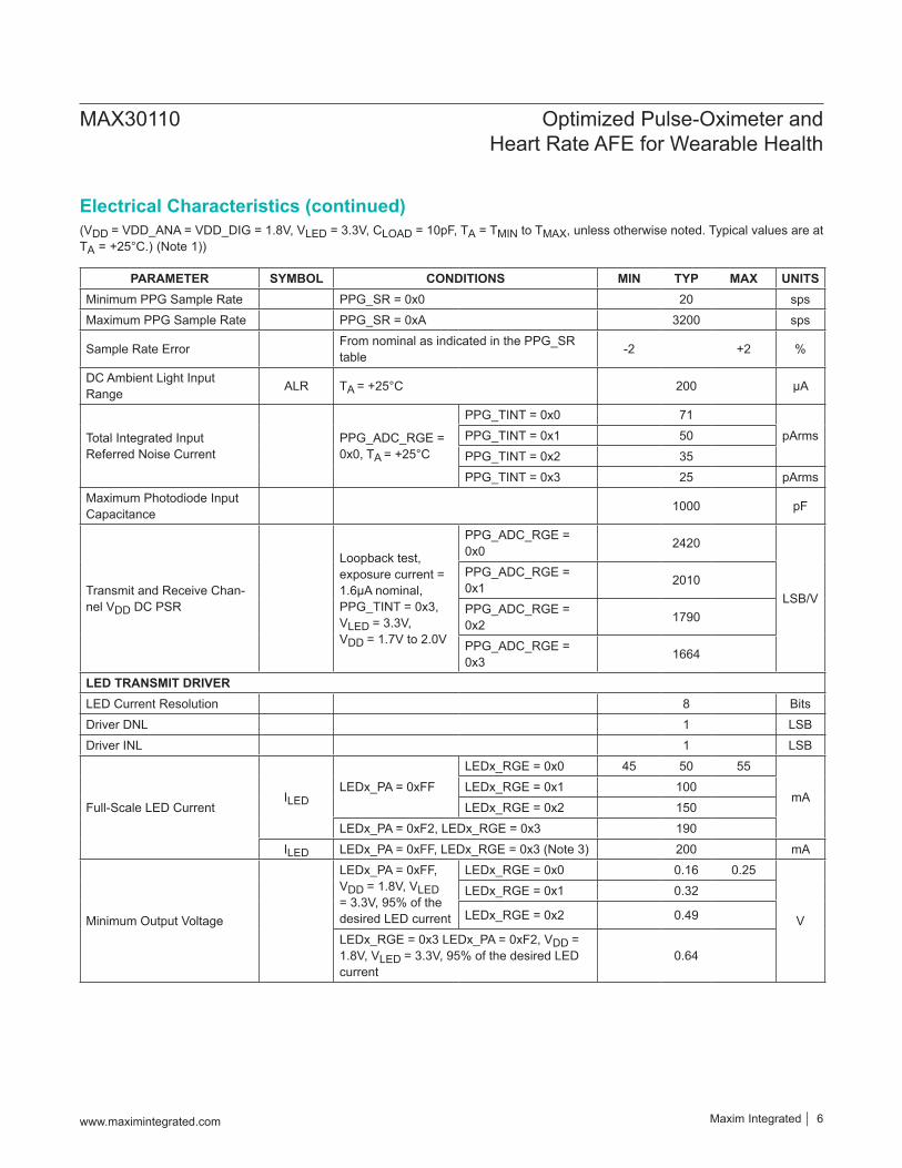
(VDD = VDD_ANA = VDD_DIG = 1.8V, VLED = 3.3V, CLOAD = 10pF, TA = TMIN to TMAX, unless otherwise noted. Typical values are at TA = +25°C.) (Note 1))
PARAMETER SYMBOL CONDITIONS MIN TYP MAX UNITSMinimum PPG Sample Rate PPG_SR = 0x0 20 spsMaximum PPG Sample Rate PPG_SR = 0xA 3200 sps
Sample Rate Error From nominal as indicated in the PPG_SR table -2 +2 %
DC Ambient Light Input Range ALR TA = +25°C 200 μA
Total Integrated Input Referred Noise Current
PPG_ADC_RGE = 0x0, TA = +25°C
PPG_TINT = 0x0 71pArmsPPG_TINT = 0x1 50
PPG_TINT = 0x2 35PPG_TINT = 0x3 25 pArms
Maximum Photodiode Input Capacitance 1000 pF
Transmit and Receive Chan-nel VDD DC PSR
Loopback test, exposure current = 1.6μA nominal,PPG_TINT = 0x3,VLED = 3.3V, VDD = 1.7V to 2.0V
PPG_ADC_RGE = 0x0 2420
LSB/V
PPG_ADC_RGE = 0x1 2010
PPG_ADC_RGE = 0x2 1790
PPG_ADC_RGE = 0x3 1664
LED TRANSMIT DRIVERLED Current Resolution 8 BitsDriver DNL 1 LSBDriver INL 1 LSB
Full-Scale LED CurrentILED
LEDx_PA = 0xFFLEDx_RGE = 0x0 45 50 55
mALEDx_RGE = 0x1 100LEDx_RGE = 0x2 150
LEDx_PA = 0xF2, LEDx_RGE = 0x3 190ILED LEDx_PA = 0xFF, LEDx_RGE = 0x3 (Note 3) 200 mA
Minimum Output Voltage
LEDx_PA = 0xFF, VDD = 1.8V, VLED = 3.3V, 95% of the desired LED current
LEDx_RGE = 0x0 0.16 0.25
V
LEDx_RGE = 0x1 0.32
LEDx_RGE = 0x2 0.49
LEDx_RGE = 0x3 LEDx_PA = 0xF2, VDD = 1.8V, VLED = 3.3V, 95% of the desired LED current
0.64
Electrical Characteristics (continued)
www.maximintegrated.com Maxim Integrated │ 6
MAX30110 Optimized Pulse-Oximeter and Heart Rate AFE for Wearable Health

(VDD = VDD_ANA = VDD_DIG = 1.8V, VLED = 3.3V, CLOAD = 10pF, TA = TMIN to TMAX, unless otherwise noted. Typical values are at TA = +25°C.) (Note 1))
PARAMETER SYMBOL CONDITIONS MIN TYP MAX UNITS
Transmit Driver VLED DC PSR
LEDx_PA = 0xFF, VDD = 1.8V, VLEDx_DRV = 0.9V, VLED = 3.1V to 5.25V
LEDx_RGE = 0x0 -0.9 -0.04 +0.9
mA/V
LEDx_RGE = 0x1 -0.06
LEDx_RGE = 0x2 -0.02
LEDx_PA = 0xF2, VDD = 1.8V, VLEDx_DRV = 0.9V, VLED = 3.1V to 5.25V
LEDx_RGE = 0x3 -0.025
Transmit Driver VDD DC PSR
LEDx_PA = 0xFF, VLED = 3.3V, VLEDx_DRV = 0.9V, VDD = 1.7V to 2.0V
LEDx_RGE = 0x0 -4 ±0.08 +4mA/V
LEDx_RGE = 0x1 0.14
LEDx_RGE = 0x2 0.16 mA/V
LEDx_PA = 0xF2, VLED = 3.3V, VLEDx_DRV = 0.9V, VDD = 1.7V to 2.0V
LEDx_RGE = 0x3 0.02 mA/V
LED Driver Compliance Interrupt LEDCOMP LEDx_RGE = 0x0, LED1_DRV only 170 mV
DIGITAL/I/O CHARACTERISTICSOutput High Voltage VOH SDO, INT, ISOURCE = 2mA VDD - 0.4 V
Output Low Voltage VOL SDO, INT, ISINK = 2mA 0.4 V
Input Voltage Low VILI SDI, SCLK, CSB, FCLK 0.3 x VDD VInput Voltage High VIH SDI, SCLK, CSB, FCLK 0.7 x VDD VInput Hysteresis VHYS SDI, SCLK, CSB, FCLK 200 mV
Pin Capacitance CPIN SDI, SCLK, CSB, INT (when inactive) 10 pF
Pin Leakage Current IPINSDA, SCLK, CSB, INT (when inactive), TA = +25°C
0.01 1 μA
DIGITAL/SPI TIMING CHARACTERISTICSSCLK Frequency fSCLK 4 MHzSCLK Period tCP 250 nsSCLK Pulse Width High tCH 75 nsSCLK Pulse Width Low tCL 75 nsCSB Fall to SCLK Rise Setup Time tCSS0 to 1st SCLK rising edge 20 ns
CSB Fall to SCLK Rise Hold Time tCSH0
Applies to inactive rising edge preceding 1st rising edge 0 ns
CSB Rise to SCLK Rise Hold Time tCSH1 Applies to 24th rising edge 500 ns
SCLK Rise to CSB Fall tCSF Applies to 24th rising edge 500 nsCSB Pulse Width High tCSPW 250 ns
Electrical Characteristics (continued)
www.maximintegrated.com Maxim Integrated │ 7
MAX30110 Optimized Pulse-Oximeter and Heart Rate AFE for Wearable Health
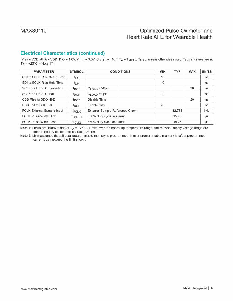
(VDD = VDD_ANA = VDD_DIG = 1.8V, VLED = 3.3V, CLOAD = 10pF, TA = TMIN to TMAX, unless otherwise noted. Typical values are at TA = +25°C.) (Note 1))
Note 1: Limits are 100% tested at TA = +25°C. Limits over the operating temperature range and relevant supply voltage range are guaranteed by design and characterization.
Note 2: Limit assumes that all user-programmable memory is programmed. If user programmable memory is left unprogrammed, currents can exceed the limit shown.
PARAMETER SYMBOL CONDITIONS MIN TYP MAX UNITSSDI to SCLK Rise Setup Time tDS 10 ns
SDI to SCLK Rise Hold Time tDH 10 ns
SCLK Fall to SDO Transition tDOT CLOAD = 20pF 20 ns
SCLK Fall to SDO Fall tDOH CLOAD = 0pF 2 ns
CSB Rise to SDO Hi-Z tDOZ Disable Time 20 ns
CSB Fall to SDO Fall tDOE Enable time 20 ns
FCLK External Sample Input fFCLK External Sample Reference Clock 32.768 kHz
FCLK Pulse Width High fFCLKH ~50% duty cycle assumed 15.26 µs
FCLK Pulse Width Low fFCLKL ~50% duty cycle assumed 15.26 µs
Electrical Characteristics (continued)
www.maximintegrated.com Maxim Integrated │ 8
MAX30110 Optimized Pulse-Oximeter and Heart Rate AFE for Wearable Health
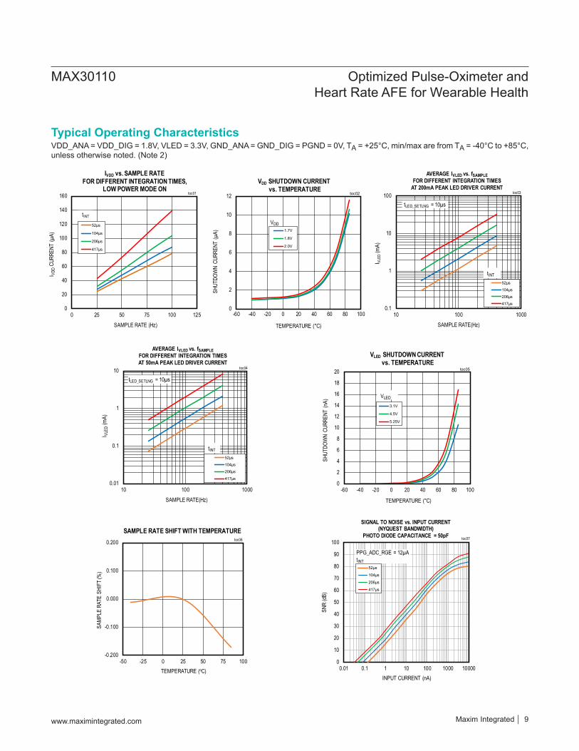
VDD_ANA = VDD_DIG = 1.8V, VLED = 3.3V, GND_ANA = GND_DIG = PGND = 0V, TA = +25°C, min/max are from TA = -40°C to +85°C, unless otherwise noted. (Note 2)
Typical Operating Characteristics
0
20
40
60
80
100
120
140
160
0 25 50 75 100 125
I VD
DCU
RREN
T(µ
A)
SAMPLE RATE (Hz)
52μs
104μs
206μs
417μs
IVDD vs. SAMPLE RATEFOR DIFFERENT INTEGRATION TIMES,
LOW POWER MODE ONtoc01
tINT
0.01
0.1
1
10
10 100 1000
I VLE
D(m
A)
SAMPLE RATE(Hz)
AVERAGE IVLED vs. fSAMPLEFOR DIFFERENT INTEGRATION TIMESAT 50mA PEAK LED DRIVER CURRENT
52μs
104μs
206μs
417μs
toc04
tLED_SETLNG = 10µs
tINT
0
2
4
6
8
10
12
-60 -40 -20 0 20 40 60 80 100
VDD
SHUT
DOW
N CU
RREN
T (µ
A)
TEMPERATURE (°C)
1.7V
1.8V
2.0V
VDD SHUTDOWN CURRENTvs. TEMPERATURE
toc02
0
2
4
6
8
10
12
14
16
18
20
-60 -40 -20 0 20 40 60 80 100
SHUT
DOW
N CU
RREN
T (n
A)
TEMPERATURE (°C)
3.1V
4.5V
5.25V
VLED SHUTDOWN CURRENTvs. TEMPERATURE
toc05
VLED
0
10
20
30
40
50
60
70
80
90
100
0.01 0.1 1 10 100 1000 10000
SNR
(dB)
INPUT CURRENT (nA)
52μs
104μs
206μs
417μs
PPG_ADC_RGE = 12µAtINT
SIGNAL TO NOISE vs. INPUT CURRENT(NYQUEST BANDWIDTH)
PHOTO DIODE CAPACITANCE = 50pFtoc07
0.1
1
10
100
10 100 1000
I VLE
D(m
A)
SAMPLE RATE(Hz)
AVERAGE IVLED vs. fSAMPLEFOR DIFFERENT INTEGRATION TIMES
AT 200mA PEAK LED DRIVER CURRENT
52μs
104μs
206μs
417μs
toc03
tLED_SETLNG = 10µs
tINT
-0.200
-0.100
0.000
0.100
0.200
-50 -25 0 25 50 75 100
SAM
PLE
RATE
SHI
FT(%
)
TEMPERATURE (oC)
SAMPLE RATE SHIFT WITH TEMPERATUREtoc06
Maxim Integrated │ 9www.maximintegrated.com
MAX30110 Optimized Pulse-Oximeter and Heart Rate AFE for Wearable Health

Bump Configurations
LED2_DRV
GND_DIG
GND_ANA
MAX30110
1 2
A
B
LED1_DRV PGND
C
N.C.
SDO
SCLK
3 4
N.C.
N.C.
VDD_DIG
CSB
N.C.
5
N.C.
SDI
PD_GND
6
PD_IN
VLED FCLK
D
N.C.VDD_ANA N.C. C2_P
VLED
LED1_DRV
FCLK
PGND
MAX30110
1 2
D
C
LED2_DRV GND_ANA
B
VDD_DIG
N.C.
N.C.
3 4
SCLK
VDD_ANA
N.C.
N.C.
N.C.
5
N.C.
C2_P
PD_IN
6
PD_GND
GND_DIG
A
SDON.C. CSB SDI
TOP VIEW (BUMPS ON BOTTOM), 0.4mm pitch
BOTTOM VIEW (BUMPS UP), 0.4mm pitch
INT
INT
www.maximintegrated.com Maxim Integrated │ 10
MAX30110 Optimized Pulse-Oximeter and Heart Rate AFE for Wearable Health
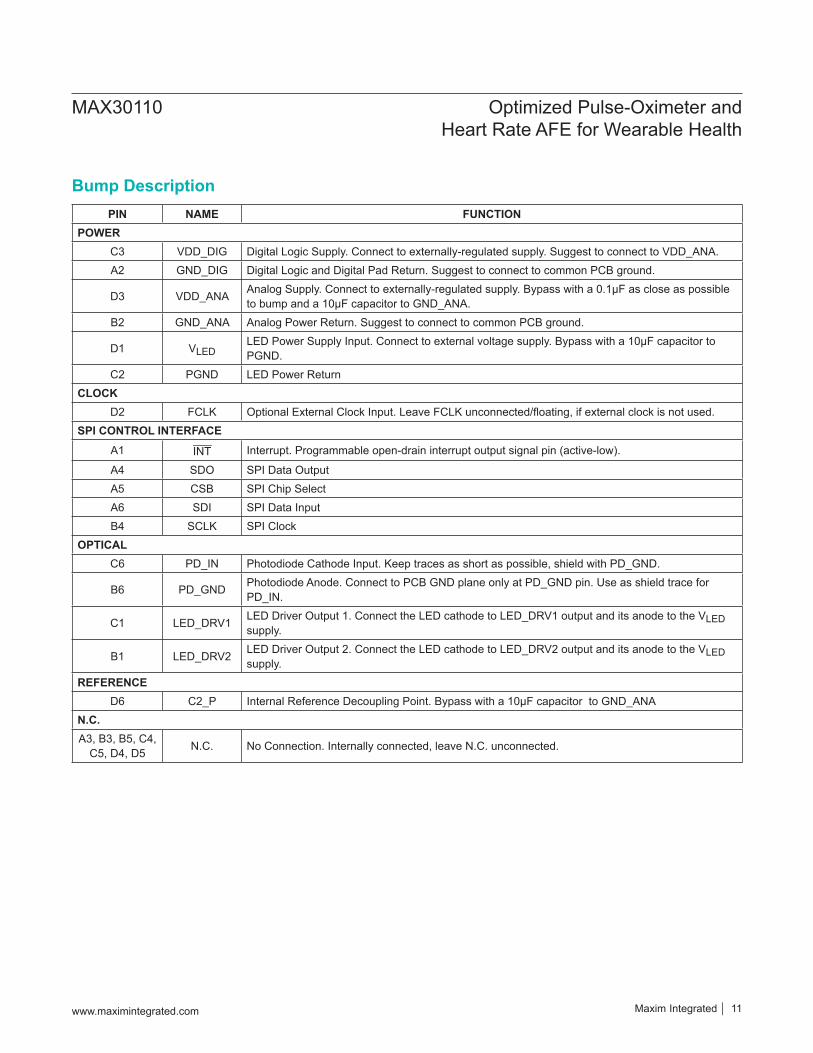
PIN NAME FUNCTIONPOWER
C3 VDD_DIG Digital Logic Supply. Connect to externally-regulated supply. Suggest to connect to VDD_ANA.A2 GND_DIG Digital Logic and Digital Pad Return. Suggest to connect to common PCB ground.
D3 VDD_ANA Analog Supply. Connect to externally-regulated supply. Bypass with a 0.1μF as close as possible to bump and a 10μF capacitor to GND_ANA.
B2 GND_ANA Analog Power Return. Suggest to connect to common PCB ground.
D1 VLEDLED Power Supply Input. Connect to external voltage supply. Bypass with a 10μF capacitor to PGND.
C2 PGND LED Power ReturnCLOCK
D2 FCLK Optional External Clock Input. Leave FCLK unconnected/floating, if external clock is not used.SPI CONTROL INTERFACE
A1 INT Interrupt. Programmable open-drain interrupt output signal pin (active-low).
A4 SDO SPI Data OutputA5 CSB SPI Chip SelectA6 SDI SPI Data InputB4 SCLK SPI Clock
OPTICALC6 PD_IN Photodiode Cathode Input. Keep traces as short as possible, shield with PD_GND.
B6 PD_GND Photodiode Anode. Connect to PCB GND plane only at PD_GND pin. Use as shield trace for PD_IN.
C1 LED_DRV1 LED Driver Output 1. Connect the LED cathode to LED_DRV1 output and its anode to the VLED supply.
B1 LED_DRV2 LED Driver Output 2. Connect the LED cathode to LED_DRV2 output and its anode to the VLED supply.
REFERENCED6 C2_P Internal Reference Decoupling Point. Bypass with a 10μF capacitor to GND_ANA
N.C.A3, B3, B5, C4,
C5, D4, D5 N.C. No Connection. Internally connected, leave N.C. unconnected.
Bump Description
www.maximintegrated.com Maxim Integrated │ 11
MAX30110 Optimized Pulse-Oximeter and Heart Rate AFE for Wearable Health
Detailed DescriptionThe MAX30110 is a complete optical pulse oximetry and heart-rate-detection, integrated, analog front-end readout circuit designed for the demanding requirements of mobile and wearable devices. Minimal external hardware components are necessary for integration into a mobile device. The MAX30110 is fully adjustable through software registers, with the digital output data being stored in a 32-samples FIFO within the IC.
Optical SubsystemThe optical subsystem in MAX30110 is composed of ambient light cancellation (ALC), a continuous-time, sigma-delta ADC, and proprietary discrete time filter. ALC incorporates a proprietary scheme to cancel ambient-light-generated photo diode current up to 200μA, allowing the sensor to work in high ambient light conditions. The ADC has programmable full-scale ranges of between 6μA and 48μA. The internal ADC is a continuous-time oversampling sigma-delta converter with 19-bit resolution. The ADC output data rate can be programmed from 20sps (samples per second) to 3200sps. The MAX30110 includes a proprietary discrete time filter to reject 50Hz/60Hz interference and changing residual ambient light from the sensor measurements.
MAX30110 supports Dynamic Power-Down mode (Low Power mode) in which the power consumption is decreased between samples. This mode is only supported for sample rates 100sps and below. For more details on the power consumption at each sample rates, please refer to the Electrical Characteristics table.
LED DriverThe MAX30110 integrates two precision LED-driver-current DACs that modulate LED pulses for both SpO2 and HR measurements. The LED current DACs have 8-bits of dynamic range with four programmable full-scale ranges of 50mA, 100mA, 150mA, and 200mA. The LED drivers are low-dropout current sources, allowing for low-noise, power-supply independent LED currents to be sourced at the lowest supply voltage possible; thus minimizing LED power consumption. The LED pulse width and the LED settling time can be programmed to allow the algorithms to optimize SpO2 and HR accuracy at the lowest dynamic power consumption dictated by the application.
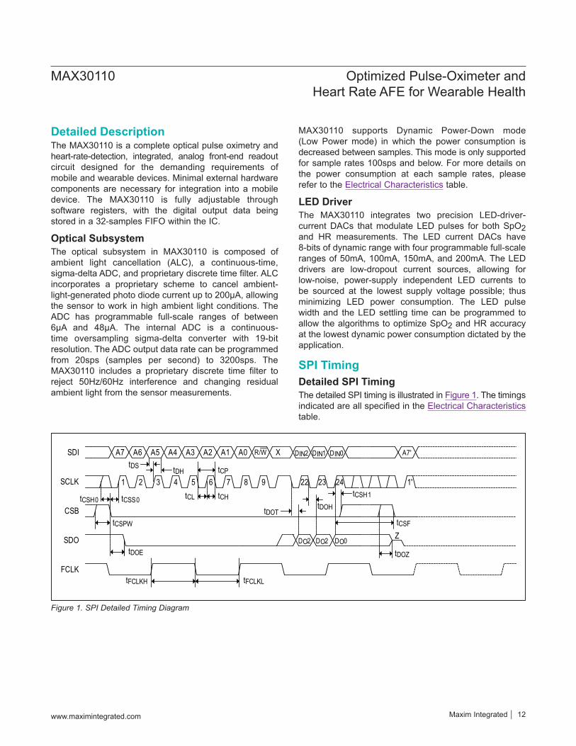
SPI TimingDetailed SPI TimingThe detailed SPI timing is illustrated in Figure 1. The timings indicated are all specified in the Electrical Characteristics table.
Figure 1. SPI Detailed Timing Diagram
A7 A6 A5 A4 A3 A2 A1 A0 X DIN2 DIN1 DIN0R/W
1 2 3 4 5 6 7 8 9 22 23 24 1'
A7'
DO2 DO2 DO0
tDS tDH
tCHtCL
tCP
tCSS0tCSH0
tDOE
tCSPW
tDOT
tCSH1
tCSF
tDOZ
tFCLKH
SDI
SCLK
CSB
SDO
FCLK
Z
tFCLKL
tDOH
www.maximintegrated.com Maxim Integrated │ 12
MAX30110 Optimized Pulse-Oximeter and Heart Rate AFE for Wearable Health

Single-Word SPI Register Read/Write TransactionThe MAX30110 interface is SPI/QSPI/Microwire/DSP compatible. The operation of the SPI interface is shown below. Data is strobed into the MAX30110 on the SCLK rising edge, while clocked-out on the SCLK falling edge. All single-word SPI read and write operations are performed in a 3-byte, 24-cycle SPI instruction framed by a CSB low interval. The content of the SPI operation consists of a one byte register address (A[7:0]), followed by a one-byte command word that defines the transaction as write or read, followed by a single-byte data word, either written to, or read from, the register location provided in the first byte.Write mode operations will be executed on the 24th SCLK rising edge using the first three bytes of data available. In
write mode, any data supplied after the 24th SCLK rising edge will be ignored. Subsequent writes require CSB to deassert high and then assert low for the next write command. A rising CSB edge precede the 24th rising edge of SCLK by tCSA (detailed SPI timing diagram), will result in the transaction being aborted.Read mode operations will access the requested data on the 16th SCLK rising edge, and present the MSB of the requested data on the following SCLK falling edge, allowing the µC to latch the data MSB on the 17th SCLK rising edge. Configuration and status registers are available through normal mode readback sequences. FIFO reads must be performed with a burst mode FIFO read (see SPI FIFO Burst Mode Read Transaction). If more than 24 SCLK rising edges are provided in a normal read sequence, the excess edges will be ignored and the device will read back zeros.
Figure 2: SPI Write Transaction Diagram
Figure 3. SPI Read Transaction Diagram
1 2 3 4 5 6 7 8 9 10 11 12 13 14 15 16 17 18 19 20 21 22 23 24
A7 A6 A5 A4 A3 A2 A1 A0 W D7 D6 D5 D4 D3 D2 D1DON’T CARE D0 DON’T CARE
Z Command Executed Ignored Edges
Z
CSB
SDI
SCLK
SDO
1 2 3 4 5 6 7 8 9 10 11 12 13 14 15 16 17 18 19 20 21 22 23 24
A7 A6 A5 A4 A3 A2 A1 A0 R
Z
Interrupt/Read Pointer Updated (If Applicable)
Ignored EdgesZ
CSB
SDI
SCLK
SDO
DON’T CARE
DO7 DO6 DO5 DO4 DO3 DO2 DO1 DO0
www.maximintegrated.com Maxim Integrated │ 13
MAX30110 Optimized Pulse-Oximeter and Heart Rate AFE for Wearable Health

SPI FIFO Burst Mode Read TransactionThe MAX30110 provides a FIFO burst read mode to increase data transfer efficiency. The first 16 SCLK cycles operate exactly as described for the normal read mode, the first byte being the register address, the second being a read command. The subsequent SCLKs consist of FIFO data, 24 SCLKs per sample. All Samples in the FIFO should be read with a single FIFO burst read command.
Each FIFO sample consists of 3 bytes per sample and thus requires 24 SCLKs per sample to readout. The first byte (SCLK 16 to 23) consists of both the sub-range DAC value (upper 5 bits, left justified) then the MSBs of the corrected exposure sample (MSB, MSB-1 and MSB-2). The next byte (SCLK 24 to 31) consists of sample bits MSB-3 to MSB-19. The final byte of each sample (SCLK 32 to 40) consists of the sample LSB bits. The number of samples in the FIFO depends on the FIFO configuration and the channels enable. See the FIFO Configuration section for more details on the FIFO configuration and readout.
Figure 4. SPI FIFO Burst Mode Transaction Diagram
N+24
1 2 3 4 5 6 7 8 9 10 11 12 13 14 15 16
A7 A6 A5 A4 A3 A2 A1 A0 R DON’T CARE
Z
CSB
SDI
SCLK
SDO
17 18 19 20 21 22 23 24 25 26 27 28 29 30 32 32 33 34 35 36 37 38 39 40
T4A
SCLK
SDO
CSB
T3A T2A T1A T0A O18A O17A O16A O15A O14A O13A O12A O11A O10A O9A O8A O7A O6A O5A O4A O3A O2A O1A O0A
N N+9
N+17
T4C
SCLK
SDO T3C T2C T1C T0C O18C O17C O16C O15C O14C O13C O12C O11C O10C O9C O8C O7C O6C O5C O4C O3C O2C O1C O0C
41 42 43 44 45 46 47 48 49 50 51 52 53 54 55 56 57 58 59 60 61 62 63 64
T4B
SCLK
SDO T3B T2B T1B T0B O18B O17B O16B O15B O14B O13B O12B O11B O10B O9B O8B O7B O6B O5B O4B O3B O2B O1B O0B
Z
www.maximintegrated.com Maxim Integrated │ 14
MAX30110 Optimized Pulse-Oximeter and Heart Rate AFE for Wearable Health

FIFO ConfigurationThe FIFO can hold up to 32 samples of data, with each sample comprised of up to 4 data Items (time slots). Each data item is 3 bytes. The content of each data item is programmed through register FD1 to FD4 (FIFO data control).These data items are ADC counts from the analog front-end of this device. The FIFO supports the following features:
● Maximum 32 samples (depth) ● Supports up to four data items in each sample ● FIFO roll-on full ● Different interrupt modes based on watermark
There are seven registers that control how the FIFO is configured and read out. These registers are described in Table 1 and Table 2.FIFO Data Control (Address 0x09 and 0x0A)The data format in the FIFO, as well as the sequencing of exposures, are controlled by the FIFO Data Control registers through FD1 through FD4. There are four FIFO data items available, each holding up to 32 samples. The exposure sequence cycles through the FIFO data bit fields, starting from FD1 to FD4. The first FIFO data field set to NONE (0000) ends the sequence.
Table 2: Data Items Type for FIFO Control RegistersFDX[3:0]* DATA TYPE FIFO DATA CONTENT NOTE
0000 NONE ― ―0001 LED1 PPG_DATA[18:0] MS bits should be masked0010 LED2 PPG_DATA[18:0] MS bits should be masked0011 Reserved ― ―0100 Reserved ― ―0101 PILOT LED1 PPG_DATA[18:0] MS bits should be masked0110 Reserved ― ―0111 Reserved ― ―1000 Reserved ― ―1001 Reserved ― ―1010 Reserved ― ―1011 Reserved ― ―1100 DIRECT_AMBIENT PPG_DATA[18:0] MS bits should be masked1101 LED1 and LED2 PPG_DATA[18:0] MS bits should be masked1110 Reserved ― ―1111 Reserved ― ―
ADDRESS REGISTER NAME DEFAULT VALUE B7 B6 B5 B4 B3 B2 B1 B00X04 FIFO Write Pointer 00 ― ― ― FIFO_WR_PTR[4:0]0X05 Overflow Counter 00 ― ― ― OVF_COUNTER[4:0]0X06 FIFO Read Pointer 00 ― ― ― FIFO_RD_PTR[4:0]0X07 FIFO Data Register 00 FIFO_DATA[7:0]0X08 FIFO Configuration 0F ― FIFO_STAT_CLR A_FULL_TYPE FIFO_RO FIFO_A_FULL[3:0]0x09 FIFO Data Control 1 00 FD2[3:0] FD1[3:0]0x0A FIFO Data Control 2 00 FD4[3:0] FD3[3:0]
* Note: In FDx, x is 1, 2, 3, or 4 for the corresponding FIFO bank.
Table 1. FIFO Information, Control and Configuration Registers
www.maximintegrated.com Maxim Integrated │ 15
MAX30110 Optimized Pulse-Oximeter and Heart Rate AFE for Wearable Health

Write Pointer (Register 0X04)FIFO_WR_PTR[4:0] points to the FIFO location where the next sample will be written. This pointer advances for each sample pushed on to the FIFO by the internal conversion process. The write pointer is a 5-bit counter and will wrap around to count 0x00 on the next sample after count 0x1F.Overflow Counter (Register 0X05)OVF_COUNTER[4:0] logs the number of samples lost if the FIFO is not read in a timely fashion. This counter holds at count value 0x1F. When a complete sample is popped from the FIFO (when the read pointer advances), and OVF_COUNTER is reset to zero. This counter is essentially a debug tool. It should be read immediately before reading the FIFO in order to check if an overflow condition has occurred.Read Pointer (Register 0X06)FIFO_RD_PTR[4:0] points to the location from where the next sample from the FIFO will be read through the inter-face. This advances each time a sample is read from the FIFO. The read pointer can be both read and written to. This allows a sample to be reread from the FIFO if it has not already been overwritten. The read pointer is updated from a 5-bit counter and will wrap around to count 0x00 from count 0x1F.FIFO Data (Register 0X07)FIFO_DATA[7:0] is a read-only register used to retrieve data from the FIFO. The format and data type of the data stored in the FIFO is determined by the FIFO data control register. Readout from the FIFO follows a progression defined by the FIFO data control register as well. This configuration is best illustrated by a few examples.Assume it is desired to perform an SpO2 measurement simultaneously with monitoring the ambient level on the photodiode to adjust the IR and red LED intensity. To perform this measurement, config the following registers, FIFO Data Control field
FD1[3:0] = 0x1 (LED1)
FD2[3:0] = 0x2 (LED2)
FD3[3:0] = 0xC (DIRECT_AMBIENT)
FD4[3:0] = 0x0 (NONE)
PPG ConfigurationPPG_ADC_RGE[1:0] (Gain Range Control)
PPG_SR[3:0] (Sample Rate Control)
PPG_TINT[1:0] (Integration Time)
LED Pulse AmplitudeLED1_PA[7:0] (LED1 Current Pulse Amplitude)
LED2_PA[7:0] (LED2 Current Pulse Amplitude)
When done so the sample sequence and the data for-mat in the FIFO will follow the following time/location sequence.
LED1 sample 1
LED2 sample 1
DIRECT_AMBIENT sample 1
LED1 sample 2
LED2 sample 2
DIRECT_AMBIENT sample 2
.
.
.
LED1 sample n
LED2 sample n
DIRECT_AMBIENT sample n
where:LED1 sample x = ambient light corrected photo-diode ADC count exposure data from LED1 for the sample xLED2 sample x = ambient light corrected photo-diode ADC count exposure data from LED2 for the sample xDIRECT_AMBIENT sample x = direct ambient sample xn is the number of samples in the FIFO, which can be up to 32 samples.
For a second example, assume it is desired to pulse LED1 and LED2 simultaneously while also monitoring the ambient level. In this case set the following registers, FIFO Data Control field
FD1[3:0] = 0xD (LED1 & LED2)
FD2[3:0] = 0xC (DIRECT_AMBIENT)
FD3[3:0] = 0x0 (NONE)
FD4[3:0] = 0x0 (NONE)
www.maximintegrated.com Maxim Integrated │ 16
MAX30110 Optimized Pulse-Oximeter and Heart Rate AFE for Wearable Health

The sequencing in the FIFO will then be,LED1 and LED2 sample1
DIRECT_AMBIENT sample 1
LED1 and LED2 sample2
DIRECT_AMBIENT 2...LED1 and LED2 sample n
DIRECT_AMBIENT n
where:LED1 and LED2 sample x = ambient light cor-rected photodiode ADC count exposure data when both LED1 and LED2 are active simulta-neuouslyDIRECT_AMBIENT sample x = direct ambient corrected sample x
The number of bytes of active data samples is given by: 3 x K x N where:
K = the number of active sampled channels as defined in the FIFO_Data_Control register 0x09 and 0x0AN = the number of active data samples in the FIFO
The number of active data samples in the FIFO is directly readable by subtracting the FIFO_RD_PTR[4:0] from the FIFO_WR_PTR[4:0], and taking wrap around of the pointers into consideration. It is typically controlled in the system by generating an interrupt on the INT line when the FIFO reaches a watermark level computed from the FIFO_A_FULL[3:0] field in the FIFO Configuration register (0x08). In this case, when the active data samples in the FIFO reach a level given by 32 - FIFO_A_FULL[3:0], an A_FULL interrupt is generated.
To calculate the number of active samples when the INT signal is asserted, execute the following pseudo-code:
read the OVF_COUNTER register
read the FIFO_WR_PTR register
read the FIFO_RD_PTR register
if (OVF_COUNTER == 0) then //no overflow occurred
if (FIFO_WR_PTR > FIFO_RD_PTR) then
NUM_AVAILABLE_SAMPLES = FIFO_WR_PTR
– FIFO_RD_PTR
else
NUM_AVAILABLE_SAMPLES = FIFO_WR_PTR + 32 - FIFO_RD_PTR
endif
elseNUM_AVAILABLE_SAMPLES = 32 // over-flow occurred and data has been lost
endif
FIFO data format depends on the data type being stored. Optical data, whether ambient-corrected LED exposure, ambient-corrected proximity, or direct ambient-sampled data is as shown in Table 3. The ADC data is left-justified at FIFO_DATA[18] and the MSBs (FIFO_DATA[23:18]) are don’t care and should be masked as shown in Table 3. In other words, the MSB bit of the ADC data is always in the bit 18 position.The ADC resolution is set by the PPG_LED_PW[1:0] in the PPG Configuration 1 Register. This field generates an ADC resolution of 19, 18, 17, or 16 bits and is tied to the selected integration time of 417μs, 206μs, 104μs, or 52μs, respectively. In lower ADC resolutions, the unused LSBs should be masked.
FIFO DATA FORMAT (FIFO_DATA[23:0])
Integration Pulse Width
ADC Res
ADC ValueF23 F22 F21 F20 F19 F18 F17 F16 F15 F14 F13 F12 F11 F10 F9 F8 F7 F6 F5 F4 F3 F2 F1 F0
417μs 19-bits X X X X X O18 O17 O16 O15 O14 O13 O12 O11 O10 O9 O8 O7 O6 O5 O4 O3 O2 O1 O0206μs 18-bits X X X X X O18 O17 O16 O15 O14 O13 O12 O11 O10 O9 O8 O7 O6 O5 O4 O3 O2 O1 X104μs 17-bits X X X X X O18 O17 O16 O15 O14 O13 O12 O11 O10 O9 O8 O7 O6 O5 O4 O3 O2 X X52μs 16-bits X X X X X O18 O17 O16 O15 O14 O13 O12 O11 O10 O9 O8 O7 O6 O5 O4 O3 X X X
Table 3. Integration Pulse Width, Resulting ADC Resolution, and FIFO Data Format
www.maximintegrated.com Maxim Integrated │ 17
MAX30110 Optimized Pulse-Oximeter and Heart Rate AFE for Wearable Health
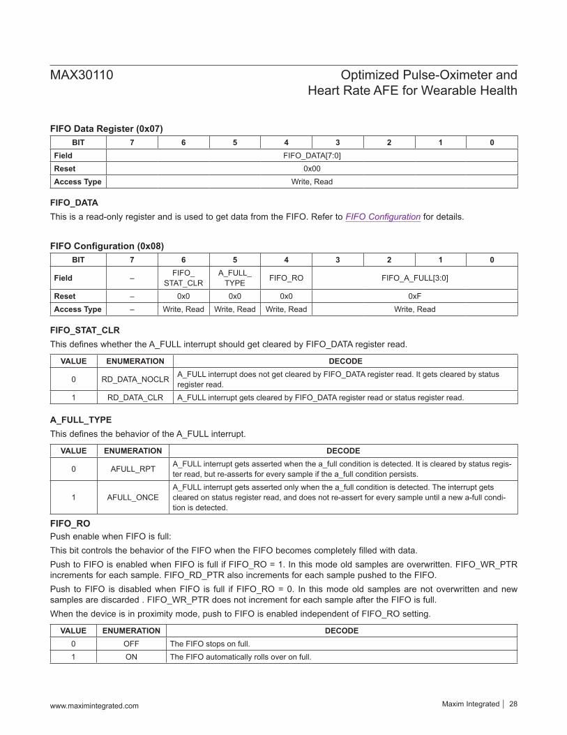
FIFO Almost Full (Watermark)The FIFO_A_FULL[3:0] register in the FIFO_Configuration register (0x08) determines when the A_FULL bit in the Interrupt_Status 1 register (0x00) gets asserted. The FIFO is almost full when it has 32 minus FIFO_A_FULL[3:0] samples. Then, if A_FULL_EN mask bit in the Interrupt_Enable 1 register (0x02) is set, the A_FULL bit in the Interrupt Status 1 will be set and routed to the INT pin on the MAX30110 interface. This condition prompts the Application Processor to read samples from the FIFO before it gets filled. The A_FULL bit is cleared and INT is deasserted when the status register is read, or when the FIFO_DATA register (0x07) is read and FIFO_STAT_CLR (0x08) bit is set.When the application processor receives an interrupt, there are at least 32 minus FIFO_A_FULL[3:0] samples available in the FIFO. It is not necessary to read the FIFO_WR_PTR and FIFO_RD_PTR registers. The Application Processor may read all the available samples in the FIFO, or only a portion of it. At high sample rates, it is recommended that only a portion of the available samples are read on an A_FULL interrupt, to ensure that FIFO reading does not happen when the next sample conversion is in progress. The remaining samples will be read on the next interrupt.If the A_FULL interrupt is not enabled, the Application Processor has to read the FIFO in polling mode. In this mode the Application Processor has to read the FIFO_WR_PTR and FIFO_RD_PTR registers to calculate the number of samples available in the FIFO, and then decide how many samples to read. However, polling mode is not recommended, because in this mode an interface transaction will inevitably overlap an optical sample, potentially adding noise to the optical data. Because of this concern, the interface transaction should occur during the dead time between optical samples to avoid adding additional noise.FIFO_RO (FIFO Rollover)The FIFO_RO bit in the FIFO_Configuration register (0x08) determines whether samples get pushed on to the FIFO when it is full. If push is enabled when FIFO is full, old samples are lost. If FIFO_RO is not set, the new sample is dropped and the FIFO is not updated.A_FULL_TYPEThe A_FULL_TYPE bit defines the behavior of the A_FULL interrupt. If the A_FULL_TYPE bit is set low, the A_FULL interrupt gets asserted when the A_FULL condition is detected and cleared by status register read, but reasserts for every sample if the A_FULL condition persists.
If A_FULL_TYPE bit is set high, the A_FULL interrupt gets asserted only when the A_FULL condition is detected. The interrupt gets cleared on status register read, and does not re-assert for every sample until a new A_FULL condition is detected.FIFO_STAT_CLRThe FIFO_STAT_CLR bit defines whether the A-FULL interrupt should get cleared by FIFO_DATA register read. If FIFO_STAT_CLR is set low, A_FULL and DATA_RDY interrupts do not get cleared by FIFO_DATA register read but get cleared by status register read. If FIFO_STAT_CLR is set high, A_FULL and DATA_RDY interrupts get cleared by a FIFO_DATA register read or a status register read.
Optical TimingThe AFE can be configured to make a variety of measurements which involves the following options:
● LED1 ● LED2 ● LED1 + LED2 ● Direct Ambient Measurement
For more details on the available modes, please refer to FIFO Configuration section.The “LED Ambient Sample” is integrated without turning on the LED, while “LED Exposure Sample” is integrated with LED illumination driven by the on-chip LED driver. Each “LED Exposure Sample” output is then compensated by the “LED Ambient Sample” at the front-end before the ADC conversion. The final FIFO exposure value for each LED mode represents an ambient corrected LED exposure signal.The controller is also configurable to measure direct ambient level for every exposure sample. The direct ambient measurement can be used to adjust the LED drive level to compensate for increased noise levels when high interfering ambient signals are present.The following optical timing diagrams illustrate the possible measurement configurations.
Sequential LED1 and LED2 Pulsing with Direct Ambient SamplingThe optical timing diagram in Figure 5 illustrates the optical timing when both LED1 and LED2 are enabled to pulse sequentially followed by a direct ambient measurement. This timing mode is an example of when measuring SpO2 with IR and red LEDs. The converted values of the optical measure-ments made by each LED followed by the converted direct ambient value will appear successively in the FIFO.
www.maximintegrated.com Maxim Integrated │ 18
MAX30110 Optimized Pulse-Oximeter and Heart Rate AFE for Wearable Health

Figure 6: Timing for Dual LED Pulsing with Direct Ambient Sampling
Figure 7: Timing for LED1 Pulsing with Direct Ambient Sampling
Figure 5. Timing for LED1 and LED2 Firing with Direct Ambient Sampling
DIRECT AMBIENTSAMPLE
LED EXPOSURE
SAMPLE
LEDAMBIENTSAMPLE
LED1_DRV
PD_SAMPLE
LED2_DRV
tPW
tLED_SETLNG
tINT
tPW
tINT
DIRECT AMBIENTSAMPLE
LED EXPOSURE
SAMPLE
LEDAMBIENTSAMPLE
tSAMPLE
NOTE: LED is on when LEDx_DRV is low
DIRECT AMBIENTSAMPLE
LED1 EXPOSURE
SAMPLE
LED1AMBIENTSAMPLE
LED1_DRV
PD_SAMPLE
LED2_DRV
tPW
tLED_SETLNG
tINT tINT
LED1 EXPOSURE
SAMPLE
LED1AMBIENTSAMPLE
tSAMPLE
NOTE: LED is on when LEDx_DRV is low
DIRECT AMBIENTSAMPLE
DIRECT AMBIENTSAMPLE
LED2 EXPOSURE
SAMPLE
LED2 AMBIENTSAMPLE
LED1 EXPOSURE
SAMPLE
LED1AMBIENTSAMPLE
LED1_DRV
PD_SAMPLE
LED2_DRV
tPW
tLED_SETLNG
tINT
tPW
tLED_SETLNG
tINT tINT
DIRECT AMBIENTSAMPLE
LED2 EXPOSURE
SAMPLE
LED2 AMBIENTSAMPLE
LED1 EXPOSURE
SAMPLE
LED1AMBIENTSAMPLE
tSAMPLE
NOTE: LED is on when LEDx_DRV is low
www.maximintegrated.com Maxim Integrated │ 19
MAX30110 Optimized Pulse-Oximeter and Heart Rate AFE for Wearable Health

Dual LED Pulsing with Direct Ambient SamplingThe optical timing diagram in Figure 6 represents both LED1 and LED2 pulsing simultaneously with direct ambient sampling enabled. This timing mode would be used when heart rate is being measured with two green LEDs. In this mode, a single optical sampled value followed by the ambient sampled value will appear in successive the FIFO locations.
LED1 Pulsing with Direct Ambient SamplingThe optical timing diagram in Figure 7 represents only LED1 pulsing during the data sampling time with direct ambient sampling enabled. This timing mode would be used when heart rate is being measured with a single green LED. In this mode a single optical sampled value followed by the ambient sampled value will appear successively in the FIFO.
Figure 8: Timing for LED1 Pulsing with No Ambient Sampling
Figure 9: Timing for LED2 Pulsing with Direct Ambient Sampling
LED1 EXPOSURE
SAMPLE
LED1AMBIENTSAMPLE
LED1_DRV
PD_SAMPLE
LED2_DRV
tPW
tLED_SETLNG
tINT
LED1 EXPOSURE
SAMPLE
LED1AMBIENTSAMPLE
tSAMPLE
NOTE: LED is on when LEDx_DRV is low
DIRECT AMBIENTSAMPLE
LED2 EXPOSURE
SAMPLE
LED2AMBIENTSAMPLE
LED1_DRV
PD_SAMPLE
LED2_DRVtLED_SETLNG
tINT
tPW
tINT
DIRECT AMBIENTSAMPLE
LED2 EXPOSURE
SAMPLE
LED2AMBIENTSAMPLE
tSAMPLE
NOTE: LED is on when LEDx_DRV is low
www.maximintegrated.com Maxim Integrated │ 20
MAX30110 Optimized Pulse-Oximeter and Heart Rate AFE for Wearable Health
LED1 Pulsing with No Ambient SamplingThe optical timing diagram in Figure 8 represents only LED1 pulsing during the data sampling time with no direct ambient sampling enabled. This timing mode would be used when heart rate is being measured with a single green LED. In this mode a single optical sampled value will appear successively in the FIFO.
LED2 Pulsing with Direct Ambient SamplingThe optical timing diagram in Figure 9 represents only LED2 firing during the data sampling time with direct
ambient sampling enabled. This timing mode would be used when heart rate is being measured with a single green LED. In this mode a single optical sampled value followed by the ambient sampled value will appear successively in the FIFO.
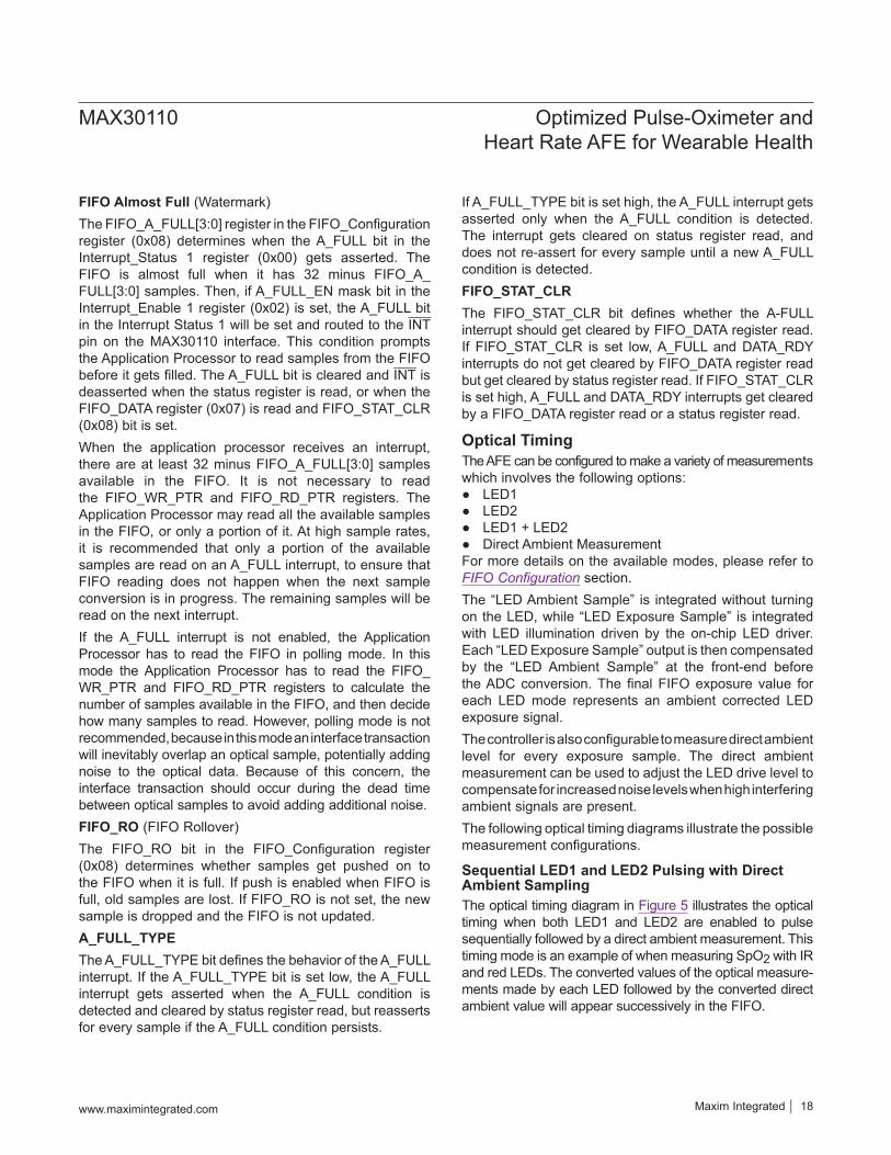
LED2 Pulsing with No Ambient SamplingThe optical timing diagram in Figure 10 represents only LED2 firing during the data sampling time with no direct ambient sampling enabled. This timing mode would be used when heart rateis being measured with a single
Figure 10: Timing for LED2 Pulsing with No Ambient Sampling
Figure 11. Readout Window for FIFO Read
LED2 EXPOSURE
SAMPLE
LED2AMBIENTSAMPLE
LED1_DRV
PD_SAMPLE
LED2_DRVtLED_SETLNG
tINT
tPW
LED2 EXPOSURE
SAMPLE
LED2AMBIENTSAMPLE
tSAMPLE
NOTE: LED is on when LEDx_DRV is low
LED EXPOSURE
SAMPLE
LEDAMBIENTSAMPLE
LED1_DRV
PD_SAMPLE
tPW
tLED_SETLNG
tINT
LED EXPOSURE
SAMPLE
LEDAMBIENTSAMPLE
tSAMPLE
Note:FD1 = LEDx
tPW = tINT + tLED_SETLNG
tSAMPLE = 1/fSAMPLE
tEXPOSURE ≈ 2*(tINT + tLED_SETLNG)
tDATA_W/R_TIME = tSAMPLE – (Number of Exposures)*(tEXPOSURE)
INT(A_FULL)
DATA/CLKACTIVITY
Data Transaction OK
tEXPOSURE
No Data TransactionNo Data Transaction
tDATA_R/W_TIME
www.maximintegrated.com Maxim Integrated │ 21
MAX30110 Optimized Pulse-Oximeter and Heart Rate AFE for Wearable Health

green LED. In this mode, a single optical sampled value will appear successively in the FIFO.
FIFO Data Read SynchronizationActivity on the interface pins can bounce the on-chip GND potential, disturbing an optical sample, resulting in higher noise. Therefore, during a FIFO read event, it is recom-mended to time the FIFO read to occur between optical samples. This can be accomplished by reading the FIFO when the FIFO_A_FULL interrupt occurs and then limit the number of samples in the FIFO to those that can be read out during the time between samples. Figure 11 illustrates how to place this read relative to the FIFO_A_FULL interrupt and the chosen sample rate, integration pulse width and LED settling time.
Proximity FunctionThe MAX30110 features proximity mode, which could significantly reduce energy consumption and extend bat-tery life. In proximity mode, LED1 is pulsing at a lower current. When an object is present, the ADC count will exceed the preset threshold (PROX_INT_THRESH) and trigger the interrupt (PROX_INT). This functionality is only available when the FD1 timing slot is assigned to LED1. To use this function, it is necessary to set four register/bit fields correctly. These variables are the normal state LED current on LED1, LED1_PA (0x11), the proximity LED cur-rent, LED_PILOT_PA (0x15), the threshold code, PROX_INT_THRESH (0x10) and the proximity mode enable bit (Interrupt Enable1 (0x02, bit 4). Note that the threshold value is the code in register PROX_INT_THRESH (0x10) times 2048.
If the proximity feature is enabled, it will be switched to proximity mode when the LED1 ADC count drops below the threshold code, PROX_INT_THRESH(0x10). At this point, the LED1 drive current will be set from LED1_PA(0x11) to LED_PILOT_PA(0x15). Note that the threshold value is the code in register PROX_INT_THRESH (0x10) times 2048. This drop in LED current should generate sufficient hysteresis to guarantee that the MAX30110 does not toggle back and forth between proximity and normal mode operation.Once in proximity mode, the MAX30110 will return to normal operating mode when the ADC count generated by the current programmed into the LED_PILOT_PA (0x15) register passes above the threshold in the PROX_INT_THRESH (0x10) register. When this occurs the LED1 current will increase to the value assigned in LED1_PA (0x11) register, again providing sufficient hysteresis to guarantee a clean transition. Note that the threshold value is the code in register PROX_INT_THRESH (0x10) times 2048.It is necessary to experiment with the specific optical geometry when configuring the proximity function. As a means of a starting point of this experimental work, it is recommended that the LED_PILOT_PA (0x15) register be set to about 1/10th the value of the LED1_PA (0x11) register. It is also recommended that the PROX_INT_THRESH (0x10) be set to roughly mid-way between the output code produced by the values of LED1_PA (0x11) and LED_PILOT_PA (0x15) when the optical device is correctly mounted to a subject.
www.maximintegrated.com Maxim Integrated │ 22
MAX30110 Optimized Pulse-Oximeter and Heart Rate AFE for Wearable Health

ADDRESS NAME MSB LSBSTATUS
0x00 Interrupt Status 1[7:0] A_FULL PPG_RDY ALC_OVF PROX_INT LED_COMPB – – PWR_RDY
0x01 Interrupt Status 2[7:0] VDD_OOR – – – – – – –
0x02 Interrupt Enable 1[7:0] A_FULL_EN
PPG_RDY_EN
ALC_OVF_EN
PROX_INT_EN
LED_COMPB_
EN– – –
0x03 Interrupt Enable 2[7:0] VDD_OOR_EN – – – – – – –
FIFO0x04 FIFO Write Pointer[7:0] – – – FIFO_WR_PTR[4:0]0x05 Overflow Counter[7:0] – – – OVF_COUNTER[4:0]0x06 FIFO Read Pointer[7:0] – – – FIFO_RD_PTR[4:0]0x07 FIFO Data Register[7:0] FIFO_DATA[7:0]
0x08 FIFO Configuration[7:0] – FIFO_STAT_CLR
A_FULL_TYPE FIFO_RO FIFO_A_FULL[3:0]
Register MapUser Register Map
www.maximintegrated.com Maxim Integrated │ 23
MAX30110 Optimized Pulse-Oximeter and Heart Rate AFE for Wearable Health

FIFO DATA CONTROL
0x09 FIFO Data Control Reg-ister 1[7:0] FD2[3:0] FD1[3:0]
0x0A FIFO Data Control Reg-ister 2[7:0] FD4[3:0] FD3[3:0]
SYSTEM CONTROL
0x0D System Control[7:0] – – – FCLK_CTRL
LP_MODE FIFO_EN SHDN RESET
PPG CONFIGURATION
0x0E PPG Configuration 1[7:0]
PPG_ADC_RGE[1:0] PPG_SR[3:0] PPG_TINT[1:0]
0x0F PPG Configuration 2[7:0] – – – LED_SETLNG[1:0] SMP_AVE[2:0]
0x10 Prox Interrupt Threshold[7:0] PROX_INT_THRESH[7:0]
LED PULSE AMPLITUDE0x11 LED1 PA[7:0] LED1_PA[7:0]0x12 LED2 PA[7:0] LED2_PA[7:0]0x14 LED Range[7:0] – – – – LED2_RGE[1:0] LED1_RGE[1:0]0x15 LED PILOT PA[7:0] PILOT_PA[7:0]
PART ID0xFF Part ID[7:0] PART_ID[7:0]
Interrupt Status 1 (0x00)BIT 7 6 5 4 3 2 1 0
Field A_FULL PPG_RDY ALC_OVF PROX_INT LED_COMPB – – PWR_RDY
Reset 0x0 0x0 0x0 0x0 0x0 – – 0x0Access Type Read Only Read Only Read Only Read Only Read Only – – Read Only
A_FULLVALUE ENUMERATION DECODE
0 OFF Normal Operation
1 ONIndicates that the FIFO buffer will overflow the threshold set by FIFO_A_FULL[3:0] on the next sample. This bit is cleared when the Interrupt Status 1 Register is read. It is also cleared when FIFO_DATA register is read, if A_FULL_CLR = 1
PPG_RDYVALUE ENUMERATION DECODE
0 OFF Normal Operation
1 ONIn LED1 and/or LED2 modes, this interrupt triggers if PPG_RDY_EN is set to 1, when there is a new sample in the data FIFO. The interrupt is cleared by reading the Interrupt Status 1 regis-ter (0x00). It is also cleared by reading the FIFO_DATA register if A_FULL_CLR is set to 1.
User Register Map continued
www.maximintegrated.com Maxim Integrated │ 24
MAX30110 Optimized Pulse-Oximeter and Heart Rate AFE for Wearable Health

ALC_OVFVALUE ENUMERATION DECODE
0 OFF Normal Operation
1 ONThis interrupt triggers when the ambient light cancellation function of the PPG photodiode has reached its maximum limit due to overflow, and therefore, ambient light is affecting the output of the ADC. The interrupt is cleared by reading the Interrupt Status 1 register (0x00).
PROX_INTVALUE ENUMERATION DECODE
0 OFF Normal Operation
1 ONIndicates that the proximity threshold has been crossed when in proximity mode. If PROX_INT is masked then the prox mode is disabled and the selected PPG mode begins immediately. This bit is cleared when the Interrupt Status 1 Register is read.
LED_COMPBLED1 is not voltage compliant meaning that VLED1 < 160mV while LED1 pulses. At the end of each sample, if the LED1 Driver is not voltage compliant, LED_COMPB interrupt is asserted if LED_COMPB_EN is set to 1. The interrupt is cleared when the status register is read.
VALUE ENUMERATION DECODE0 COMPLIANT LED1 driver voltage is in compliance1 NOT_COMPLIANT LED1 driver voltage is not in compliance
PWR_RDYVALUE ENUMERATION DECODE
0 OFF Normal Operation
1 ON Indicates that VDD_DIG went below the 1.55V under voltage lockout threshold. This bit is also set upon a soft reset.This bit is cleared when Interrupt Status 1 Register is read.
Interrupt Status 2 (0x01)BIT 7 6 5 4 3 2 1 0
Field VDD_OOR – – – – – – –Reset 0x0 – – – – – – –Access Type Read Only – – – – – – –
VDD_OORThis is an indicator to check if the VDD_ANA supply voltage is within supported range.
VALUE ENUMERATION DECODE0 OFF VDD_ANA within supported range.
1 ONIndicates that VDD_ANA is greater than 2.05V or less than 1.65V. This bit is automatically cleared when the Interrupt Status 2 register is read. The detection circuitry has a 10ms delay time, and will continue to trigger as long as the VDD_ANA is out of range.
www.maximintegrated.com Maxim Integrated │ 25
MAX30110 Optimized Pulse-Oximeter and Heart Rate AFE for Wearable Health

Interrupt Enable 1 (0x02)BIT 7 6 5 4 3 2 1 0
Field A_FULL_EN PPG_RDY_EN
ALC_OVF_EN
PROX_INT_EN
LED_COMPB_EN – – –
Reset 0x0 0x0 0x0 0x0 0x0 – – –Access Type Write, Read Write, Read Write, Read Write, Read Write, Read – – –
A_FULL_ENVALUE ENUMERATION DECODE
0 OFF A_FULL interrupt is disabled1 ON A_FULL interrupt in enabled
PPG_RDY_ENVALUE ENUMERATION DECODE
0 OFF PPG_RDY interrupt is disabled1 ON PPG_RDY interrupt is enabled.
ALC_OVF_ENVALUE ENUMERATION DECODE
0 OFF ALC_OVF interrupt is disabled1 ON ALC_OVF interrupt in enabled
PROX_INT_ENWhen this is enabled, program LED1 into FD1 in FIFO Data Control register 1. LED1 must be used for proximity detection. If the ADC reading for this exposure is below 2048 times the threshold programmed in PROX_INT_THRESH register, the device is in proximity mode, otherwise it is in normal mode.When the device is in proximity mode, the device starts data acquisition using only one exposure of LED1 and the LED current programmed in PILOT_PA register.When the device is in normal mode, the device starts data acquisition using all the exposures programmed in the FIFO Data Control registers and appropriate LED currents.When PROX_INT_EN is programmed to 1, PROX_INT interrupt is asserted when the devices enters normal mode (exit Proximity mode).
VALUE ENUMERATION DECODE0 OFF PROX_INT interrupt is disabled1 ON PROX_INT interrupt in enabled
LED_COMPB_ENVALUE ENUMERATION DECODE
0 DISABLE LED1 driver voltage compliance interrupt is disabled1 ENABLE LED1 driver voltage compliance interrupt is enabled
www.maximintegrated.com Maxim Integrated │ 26
MAX30110 Optimized Pulse-Oximeter and Heart Rate AFE for Wearable Health

Interrupt Enable 2 (0x03)BIT 7 6 5 4 3 2 1 0
Field VDD_OOR_EN – – – – – – –
Reset 0x0 – – – – – – –Access Type Write, Read – – – – – – –
VDD_OOR_ENVALUE ENUMERATION DECODE
0 OFF Disables the VDD_OVR interrupt1 ON Enables the VDD_OVR interrupt
FIFO Write Pointer (0x04)BIT 7 6 5 4 3 2 1 0
Field – – – FIFO_WR_PTR[4:0]Reset – – – 0x00Access Type – – – Write, Read
FIFO_WR_PTRThis points to the location where the next sample will be written. This pointer advances for each sample pushed on to the FIFO. Refer to FIFO Configuration for details.
Overflow Counter (0x05)BIT 7 6 5 4 3 2 1 0
Field – – – OVF_COUNTER[4:0]Reset – – – 0x00Access Type – – – Read Only
OVF_COUNTERWhen FIFO is full any new samples will result in new or old samples getting lost depending on FIFO_RO. OVF_COUNTER counts the number of samples lost. It saturates at 0x1F. Refer to FIFO Configuration for details.
FIFO Read Pointer (0x06)BIT 7 6 5 4 3 2 1 0
Field – – – FIFO_RD_PTR[4:0]Reset – – – 0x00Access Type – – – Write, Read
FIFO_RD_PTRThe FIFO Read Pointer points to the location from where the processor gets the next sample from the FIFO. This advances each time a sample is popped from the FIFO. The processor can also write to this pointer after reading the samples. This allows rereading (or retrying) samples from the FIFO Refer to FIFO Configuration for details.
www.maximintegrated.com Maxim Integrated │ 27
MAX30110 Optimized Pulse-Oximeter and Heart Rate AFE for Wearable Health
FIFO Data Register (0x07)BIT 7 6 5 4 3 2 1 0
Field FIFO_DATA[7:0]Reset 0x00Access Type Write, Read
FIFO_DATAThis is a read-only register and is used to get data from the FIFO. Refer to FIFO Configuration for details.
FIFO Configuration (0x08)BIT 7 6 5 4 3 2 1 0
Field – FIFO_STAT_CLR
A_FULL_TYPE FIFO_RO FIFO_A_FULL[3:0]
Reset – 0x0 0x0 0x0 0xFAccess Type – Write, Read Write, Read Write, Read Write, Read
FIFO_STAT_CLRThis defines whether the A_FULL interrupt should get cleared by FIFO_DATA register read.
VALUE ENUMERATION DECODE
0 RD_DATA_NOCLR A_FULL interrupt does not get cleared by FIFO_DATA register read. It gets cleared by status register read.
1 RD_DATA_CLR A_FULL interrupt gets cleared by FIFO_DATA register read or status register read.
A_FULL_TYPEThis defines the behavior of the A_FULL interrupt.
VALUE ENUMERATION DECODE
0 AFULL_RPT A_FULL interrupt gets asserted when the a_full condition is detected. It is cleared by status regis-ter read, but re-asserts for every sample if the a_full condition persists.
1 AFULL_ONCEA_FULL interrupt gets asserted only when the a_full condition is detected. The interrupt gets cleared on status register read, and does not re-assert for every sample until a new a-full condi-tion is detected.
FIFO_ROPush enable when FIFO is full:This bit controls the behavior of the FIFO when the FIFO becomes completely filled with data.Push to FIFO is enabled when FIFO is full if FIFO_RO = 1. In this mode old samples are overwritten. FIFO_WR_PTR increments for each sample. FIFO_RD_PTR also increments for each sample pushed to the FIFO.Push to FIFO is disabled when FIFO is full if FIFO_RO = 0. In this mode old samples are not overwritten and new samples are discarded . FIFO_WR_PTR does not increment for each sample after the FIFO is full.When the device is in proximity mode, push to FIFO is enabled independent of FIFO_RO setting.
VALUE ENUMERATION DECODE0 OFF The FIFO stops on full.1 ON The FIFO automatically rolls over on full.
www.maximintegrated.com Maxim Integrated │ 28
MAX30110 Optimized Pulse-Oximeter and Heart Rate AFE for Wearable Health

FIFO_A_FULLThese bits indicate how many unread samples are in the FIFO when the interrupt is asserted. For example, if set to 0xF, the interrupt triggers when there are 17 data samples in the FIFO (15 empty spaces lefts).
FIFO_A_FULL[3:0] FREE SPACES AT INTERRUPT # OF SAMPLES IN FIFO0000 0 320001 1 310010 2 300011 3 29---- ---- ----
1110 14 181111 15 17
FIFO Data Control Register 1 (0x09)BIT 7 6 5 4 3 2 1 0
Field FD2[3:0] FD1[3:0]Reset 0x0 0x0Access Type Write, Read Write, Read
FD2These bits set the data type for Data Item 2 of the FIFO.See FIFO Configuration for mode information.
FD1These bits set the data type for Data Item 1 of the FIFO.See FIFO Configuration for mode information.
FIFO Data Control Register 2 (0x0A)BIT 7 6 5 4 3 2 1 0
Field FD4[3:0] FD3[3:0]Reset 0x0 0x0Access Type Write, Read Write, Read
FD4These bits set the data type for Data Item 4 of the FIFO.See FIFO Configuration for mode information.
FD3These bits set the data type for Data Item 3 of the FIFO.See FIFO Configuration for mode information.
www.maximintegrated.com Maxim Integrated │ 29
MAX30110 Optimized Pulse-Oximeter and Heart Rate AFE for Wearable Health

System Control (0x0D)BIT 7 6 5 4 3 2 1 0
Field – – – FCLK_CTRL LP_MODE FIFO_EN SHDN RESET
Reset – – – 0x0 0x0 0x0 0x0 0x0Access Type – – – Write, Read Write, Read Write, Read Write, Read Write, Read
FCLK_CTRLFCLK pin can be used for external 32kHz clock input when the PPG sample rate is 100sps and below. Used to synchronous multiple devices into one Clock domain.
VALUE ENUMERATION DECODE
0x0 FCLK pin is not used.Use internal 32KHz clock for PPG sample rates 100Hz and below.
0x1 Use external 32KHz clock at FCLK input for PPG sample rates 100Hz and below.
LP_MODEIn low power mode, the sensor can be dynamically powered down between samples to conserve power. This dynamic power-down mode option only supports samples rates of 100Hz and below.
VALUE ENUMERATION DECODE0 OFF Dynamic power-down is disabled
1 ONDynamic power down is enabled. The device automatically enters low power mode between samples for samples rates 100Hz and below.This mode is not available for higher sample rates.
FIFO_EN
VALUE ENUMERATION DECODE
0 OFFPush to FIFO is disabled, but the read and write pointers and the data in the FIFO are all held at their values before FIFO_EN is set to 0. The conversion and LED drivers are active until FD1 is set to NONE
1 ONThe FIFO is enabled. When this bit is set the FIFO is flushed of all old data and the new samples start loading from pointer zero. Setting this bit starts conversions and LED drivers enable according to the FDx settings.
SHDNThe part can be put into a power-save mode by setting this bit to one. While in power-save mode, all registers retain their values, and write/read operations function as normal. All interrupts are cleared to zero in this mode.
VALUE ENUMERATION DECODE0 OFF The part is in normal operation. No action taken.
1 ON
The part can be put into a power-save mode by writing a ‘1’ to this bit. While in this mode all registers remain accessible and retain their data. ADC conversion data contained in the registers are previous values. Writeable registers also remain accessible in shutdown. All interrupts are cleared. In this mode the oscillator is shutdown and the part draws minimum current. If this bit is asserted during an active conversion then the conversion completes before the part shuts down.
www.maximintegrated.com Maxim Integrated │ 30
MAX30110 Optimized Pulse-Oximeter and Heart Rate AFE for Wearable Health

RESETVALUE ENUMERATION DECODE
0 OFF The part is in normal operation. No action taken.
1 ONThe part undergoes a forced power-on-reset sequence. All configuration, threshold and data registers are reset to their power-on-state. This bit then automatically becomes ‘0’ after the reset sequence is completed.
PPG Configuration 1 (0x0E)BIT 7 6 5 4 3 2 1 0
Field PPG_ADC_RGE[1:0] PPG_SR[3:0] PPG_TINT[1:0]Reset 0x0 0x0 0x0Access Type Write, Read Write, Read Write, Read
PPG_ADC_RGEThese bits set the ADC range of the photodiode sensor as shown in the table below.
PPG_ADC_RGE[1:0] LSB (pA) FULL SCALE (µA)00 11.4 601 22.9 1210 45.8 2411 91.6 48
PPG_SRThese bits set the effective sampling rate of the PPG sensor as shown in the table below.In Dual Pulse mode there are two pulses per sample, and the pulses are spaced to produce an additional 20dB of ambi-ent rejection for indoor lighting cases (100Hz or 120Hz rejection).If the sample rate, integration time, and number of Data Item are set to an invalid combination, the highest available sample rate will be automatically set for the integration and number of exposure setting. The user can read this register to confirm the sample rate.
PPG_SR[3:0] fSAMPLE (SPS) DUAL-PULSE MODE0000 20 No0001 25 No0010 50 No0011 84 No0100 100 No0101 200 No0110 400 No0111 800 No1000 1000 No1001 1600 No1010 3200 No1011 20 Yes1100 25 Yes1101 50 Yes1110 84 Yes1111 100 Yes
www.maximintegrated.com Maxim Integrated │ 31
MAX30110 Optimized Pulse-Oximeter and Heart Rate AFE for Wearable Health

See the following table for the maximum sample rates supported for all the integration time and number of Data Items.NUMBER OF DATA ITEM PER SAMPLE PPG_TINT = 0 (50µs) PPG_TINT = 1 (100µs) PPG_TINT = 2 (200µs) PPG_TINT = 3 (400µs)
1 DATA ITEM, SINGLE PULSE MODE 3200 1600 1600 1000
2 DATA ITEMS, SINGLE PULSE MODE 1600 800 800 400
3 DATA ITEMS, SINGLE PULSE MODE 1000 800 400 200
4 DATA ITEMS, SINGLE PULSE MODE 1000 400 400 200
1 DATA ITEM, DUAL PULSE MODE 100 100 100 100
2 DATA ITEMS, DUAL PULSE MODE
100 for LP_MODE = 0,50 for LP_MODE = 1
100 for LP_MODE = 0;50 for LP_MODE = 1
84 for LP_MODE = 0;50 for LP_MODE = 1
84 for LP_MODE = 0;50 for LP_MODE = 1
3 DATA ITEMS, DUAL PULSE MODE 50 50 50 50
4 DATA ITEMS, DUAL PULSE MODE
50 for LP_MODE = 0; 25 for LP_MODE= 1
50 for LP_MODE = 0;25 for LP_MODE = 1 25 25
PPG_TINTThese bits set the integration time of PPG ADC as well as the pulse width of the LEDS as shown in the table below.tLED_SETLNG is the delay programmed in the LED_SETLNG[1:0] register.
PPG_TINT[1:0] tPW, LED PULSE WIDTH (µs) tINT, INTEGRATION TIME (µs) RESOLUTION BITS
00 52 + tLED_SETLNG 52 1601 104 + tLED_SETLNG 104 1710 206 + tLED_SETLNG 206 1811 417 + tLED_SETLNG 417 19
PPG Configuration 2 (0x0F)BIT 7 6 5 4 3 2 1 0
Field – – – LED_SETLNG[1:0] SMP_AVE[2:0]Reset – – – 0x3 0x0Access Type – – – Write, Read Write, Read
LED_SETLNGDelay from rising edge of LED to start of ADC integration. This allows for the LED current to settle before the start of ADC integration.
LED_SETLNG[1:0] DELAY tLED_SETLNG (ms)00 2.501 5.010 10.011 20.0
www.maximintegrated.com Maxim Integrated │ 32
MAX30110 Optimized Pulse-Oximeter and Heart Rate AFE for Wearable Health

SMP_AVEAdjacent samples (in each individual channel) can be internally averaged to reduce the amount of data throughput.These bits set the number of samples that are averaged on chip before being written to the FIFO. The effective output sample rate is the PPG_SR rate divided by the SMP_AVE value.
SMP_AVE[2:0] SAMPLE AVERAGE000 1 (no averaging)001 2010 4011 8100 16101 32110 32111 32
Prox Interrupt Threshold (0x10)BIT 7 6 5 4 3 2 1 0
Field PROX_INT_THRESH[7:0]Reset 0x00Access Type Write, Read
PROX_INT_THRESHThis register sets the LED1 ADC count value that will trigger the transition between proximity mode to normal mode. The threshold is defined as the 8 MSB bits of the ADC count. For example, if PROX_INT_THRESH[7:0] = 0x01, then an ADC value of 2048 (decimal) or higher triggers the PROX interrupt. If PROX_INT_THRESH[7:0] = 0xFF, then only a saturated ADC triggers the interrupt.See the Proximity Function section in the detailed description for more details on the operation of proximity mode.
LED1 PA (0x11)BIT 7 6 5 4 3 2 1 0
Field LED1_PA[7:0]Reset 0x00Access Type Write, Read
www.maximintegrated.com Maxim Integrated │ 33
MAX30110 Optimized Pulse-Oximeter and Heart Rate AFE for Wearable Health

LED1_PAThese bits set the nominal peak current pulse amplitude of LEDx_DRV pin as shown in the table below.Note: x denotes the respective LED channel.
LEDX_RGE[1:0] 00 01 10 11LEDx_PA[7:0] ILEDx_DRV (mA) ILEDx_DRV (mA) ILEDx_DRV (mA) ILEDx_DRV (mA)
0x00 0 0 0 00x01 0.2 0.4 0.6 0.80x02 0.4 0.8 1.2 1.60x03 0.6 1.2 1.8 2.4
............0xFC 49.4 98.8 148.2 197.60xFD 49.6 99.2 148.8 198.40xFE 49.8 99.6 149.4 198.20xFF 50 100 150 200LSB 0.196 0.392 0.588 0.784
LED2 PA (0x12)BIT 7 6 5 4 3 2 1 0
Field LED2_PA[7:0]Reset 0x00Access Type Write, Read
LED2_PARefer to LED1_PA[1:0] for more details.
LED Range (0x14)BIT 7 6 5 4 3 2 1 0
Field – – – – LED2_RGE[1:0] LED1_RGE[1:0]Reset – – – – 0x00 0x00Access Type – – – – Write, Read Write, Read
LED2_RGERange selection of the LED 2 current.Refer to LED1_PA[1:0] for more details.
LED2_RGE[1:0] MAX LED CURRENT RANGE (mA)00 5001 10010 15011 200
www.maximintegrated.com Maxim Integrated │ 34
MAX30110 Optimized Pulse-Oximeter and Heart Rate AFE for Wearable Health

LED1_RGERange selection of the LED 1 current.Refer to LED1_PA[1:0] for more details.
LED1_RGE[1:0] MAX LED CURRENT RANGE (mA)00 5001 10010 15011 200
LED PILOT PA (0x15)BIT 7 6 5 4 3 2 1 0
Field PILOT_PA[7:0]Reset 0x00Access Type Write, Read
PILOT_PAIn proximity mode, PILOT_PA[7:0] sets LED1 proximity mode current. These bits set the current pulse amplitude for proximity mode as shown in the table below. In proximity mode, LED1_RGE[1:0] and PILOT_PA[1:0] sets the LED1_DRV current.See Proximity Function for more details on the operation of proximity mode.
LED1_RGE[1:0] 00 01 10 11PILOT_PA[7:0] ILED1_DRV (mA) ILED1_DRV (mA) ILED1_DRV (mA) ILED1_DRV (mA)
0x00 0 0 0 00x01 0.2 0.4 0.6 0.80x02 0.4 0.8 1.2 1.60x03 0.6 1.2 1.8 2.4
............0xFC 49.4 98.8 148.2 197.60xFD 49.6 99.2 148.8 198.40xFE 49.8 99.6 149.4 199.20xFF 50 100 150 200LSB 0.2 0.4 0.6 0.8
Part ID (0xFF)BIT 7 6 5 4 3 2 1 0
Field PART_ID[7:0]Reset 0x20Access Type Read Only
PART_IDThis register stores the part identifier for the chip.
www.maximintegrated.com Maxim Integrated │ 35
MAX30110 Optimized Pulse-Oximeter and Heart Rate AFE for Wearable Health

PART TEMP. RANGE BUMP-PACKAGE
MAX30110EWG+ -40°C to +85°C 24-bump, WLP 2.8mm x 2.0mm, 0.4mm Pitch
+Denotes a lead(Pb)-free/RoHS-compliant package
GND_ANA GND_DIG
0.1µF
VLED
PD_GND
PD_IN
LED1_DRV
LED2_DRV
1.0µF
C2_P
SDISDO
INT
VDD_DIGVDD_ANA
PGND
19-BIT CURRENT
ADC
AMBIENT CANCELLATION
DIGITAL NOISE CANCELLATION
32 SAMPLE FIFO
LED DRIVERS
REFERENCE
MAX30110
10µF
SPI I
NTE
RFA
CE
10µF
3.3V note3
1.8V
VDDIO note 2
Note 1: The value of INT pull up resistor should be based on the system design.
Note 2: VDDIO is the system I/O voltage supply.
Note 3: VLED is the LED power supply input, it should be based on the specifications of the LED used.Note 4: Optional External Clock input. Leave FCLK unconnected/floating, if external clock is not used.
R no
te1
FCLK RTC_CLK note 4
SCLKCSb
HO
ST
PRO
CES
SOR
Typical Application Circuit
Ordering Information
www.maximintegrated.com Maxim Integrated │ 36
MAX30110 Optimized Pulse-Oximeter and Heart Rate AFE for Wearable Health

REVISIONNUMBER
REVISIONDATE DESCRIPTION PAGES
CHANGED0 6/17 Initial release —
Revision History
Maxim Integrated cannot assume responsibility for use of any circuitry other than circuitry entirely embodied in a Maxim Integrated product. No circuit patent licenses are implied. Maxim Integrated reserves the right to change the circuitry and specifications without notice at any time. The parametric values (min and max limits) shown in the Electrical Characteristics table are guaranteed. Other parametric values quoted in this data sheet are provided for guidance.
Maxim Integrated and the Maxim Integrated logo are trademarks of Maxim Integrated Products, Inc. © 2017 Maxim Integrated Products, Inc. │ 37
MAX30110 Optimized Pulse-Oximeter and Heart Rate AFE for Wearable Health
For pricing, delivery, and ordering information, please contact Maxim Direct at 1-888-629-4642, or visit Maxim Integrated’s website at www.maximintegrated.com.


![Measurement of Heart Rate Using …measure another vital sign, heart rate. Apart from indicating the soundness of the heart, heart rate helps assessing the cardiovascular system [1].](https://static.fdocuments.us/doc/165x107/5e52a390a714512a3519c177/measurement-of-heart-rate-using-measure-another-vital-sign-heart-rate-apart-from.jpg)