MAX17598/MAX17599 ow I Q ideInpt ange Actie lamp rrentMode ...€¦ · MAX17598/MAX17599 ow I Q...
24
MAX17598/MAX17599 Low I Q , Wide-Input Range, Active Clamp Current-Mode PWM Controllers Ordering Information appears at end of data sheet. For related parts and recommended products to use with this part, refer to www.maximintegrated.com/MAX17598.related. General Description The MAX17598/MAX17599 low I Q , active clamp current- mode PWM controllers contain all the control circuitry required for the design of wide-input isolated/non-iso- lated forward-converter industrial power supplies. The MAX17598 is well-suited for universal input (rectified 85V AC to 265V AC) or telecom (36V DC to 72V DC) power supplies. The MAX17599 is optimized for low-voltage industrial supplies (4.5V DC to 36V DC). The devices include an AUX driver that drives an aux- iliary MOSFET (clamp switch) that helps implement the active-clamp transformer reset topology for forward con- verters. Such a reset topology has several advantages including reduced voltage stress on the switches, trans- former size reduction due to larger allowable flux swing, and improved efficiency due to elimination of dissipative snubber circuitry. Programmable dead time between the AUX and main driver allows for zero voltage switching (ZVS). The switching frequency is programmable from 100kHz to 1MHz for the devices with an accuracy of Q8% using an external resistor. This allows optimization of the magnetic and filter components, resulting in com- pact, cost-effective isolated/nonisolated power supplies. For EMI-sensitive applications, the ICs incorporate a programmable frequency-dithering scheme, enabling low-EMI spread-spectrum operation. An input undervoltage lockout (EN/UVLO) is provided for programming input-supply start voltage, and to ensure proper operation during brownout conditions. EN/UVLO input is also used to turn on/off the ICs. Input overvoltage (OVI) protection scheme is provided to make sure that the regulator shuts down when input supply exceeds its maximum allowed value. To control inrush current, the devices incorporate an SS pin to set the soft-start time for the regulators. Power dissipa- tion under fault conditions is minimized by hiccup overcur- rent protection (hiccup mode). Soft-stop feature provides safe discharging of the clamp capacitor when the device is turned off, and allows the controller to restart in a well- controlled manner. Additionally, negative current limit is provided in the current-sense circuitry, helping limit clamp switch current under dynamic operating conditions. SYNC feature is provided to synchronize multiple convert- ers to a common external clock in noise-sensitive applica- tions. Overtemperature fault triggers thermal shutdown for reliable protection of the device. The ICs are available in a 16-pin, TQFN package with 0.5 mm lead spacing. Benefits and Features S Active Clamp, Peak Current-Mode Forward PWM Controller S 20 FA Startup Current in UVLO S 4.5V to 36V Input-Supply Operating Range (MAX17599) S Programmable Input Undervoltage Lockout S Programmable Input Overvoltage Protection S Programmable 100kHz to 1MHz Switching Frequency S Switching Frequency Synchronization S Programmable Frequency Dithering for Low EMI Spread-Spectrum Operation S Programmable Dead Time S Adjustable Soft-Start S Programmable Slope Compensation S Fast Cycle-by-Cycle Peak-Current-Limit S 70ns Internal Leading-Edge Current-Sense Blanking S Hiccup Mode Output Short-Circuit Protection S Soft-Stop for Well-Controlled Clamp Capacitor Discharge S Negative Clamp-Switch Current Limit S 3mm x 3mm, Lead-Free 16-Pin TQFN S -40°C to +125°C Operating Temperature Range Applications Telecom and Datacom Power Supplies Isolated Battery Chargers Servers and Embedded Computing Industrial Power Supplies 19-6179; Rev 2; 4/14 EVALUATION KIT AVAILABLE For pricing, delivery, and ordering information, please contact Maxim Direct at 1-888-629-4642, or visit Maxim’s website at www.maximintegrated.com.
Transcript of MAX17598/MAX17599 ow I Q ideInpt ange Actie lamp rrentMode ...€¦ · MAX17598/MAX17599 ow I Q...

MAX17598/MAX17599
Low IQ, Wide-Input Range, Active Clamp Current-Mode PWM Controllers
Ordering Information appears at end of data sheet.
For related parts and recommended products to use with this part, refer to www.maximintegrated.com/MAX17598.related.
General Description
The MAX17598/MAX17599 low IQ, active clamp current-mode PWM controllers contain all the control circuitry required for the design of wide-input isolated/non-iso-lated forward-converter industrial power supplies. The MAX17598 is well-suited for universal input (rectified 85V AC to 265V AC) or telecom (36V DC to 72V DC) power supplies. The MAX17599 is optimized for low-voltage industrial supplies (4.5V DC to 36V DC).
The devices include an AUX driver that drives an aux-iliary MOSFET (clamp switch) that helps implement the active-clamp transformer reset topology for forward con-verters. Such a reset topology has several advantages including reduced voltage stress on the switches, trans-former size reduction due to larger allowable flux swing, and improved efficiency due to elimination of dissipative snubber circuitry. Programmable dead time between the AUX and main driver allows for zero voltage switching (ZVS).
The switching frequency is programmable from 100kHz to 1MHz for the devices with an accuracy of Q8% using an external resistor. This allows optimization of the magnetic and filter components, resulting in com-pact, cost-effective isolated/nonisolated power supplies. For EMI-sensitive applications, the ICs incorporate a programmable frequency-dithering scheme, enabling low-EMI spread-spectrum operation.
An input undervoltage lockout (EN/UVLO) is provided for programming input-supply start voltage, and to ensure proper operation during brownout conditions. EN/UVLO input is also used to turn on/off the ICs. Input overvoltage (OVI) protection scheme is provided to make sure that the regulator shuts down when input supply exceeds its maximum allowed value.
To control inrush current, the devices incorporate an SS pin to set the soft-start time for the regulators. Power dissipa-tion under fault conditions is minimized by hiccup overcur-rent protection (hiccup mode). Soft-stop feature provides safe discharging of the clamp capacitor when the device is turned off, and allows the controller to restart in a well-controlled manner. Additionally, negative current limit is provided in the current-sense circuitry, helping limit clamp switch current under dynamic operating conditions.
SYNC feature is provided to synchronize multiple convert-ers to a common external clock in noise-sensitive applica-tions. Overtemperature fault triggers thermal shutdown for reliable protection of the device. The ICs are available in a 16-pin, TQFN package with 0.5 mm lead spacing.
Benefits and Features
S Active Clamp, Peak Current-Mode Forward PWM Controller
S 20FA Startup Current in UVLO
S 4.5V to 36V Input-Supply Operating Range (MAX17599)
S Programmable Input Undervoltage Lockout
S Programmable Input Overvoltage Protection
S Programmable 100kHz to 1MHz Switching Frequency
S Switching Frequency Synchronization
S Programmable Frequency Dithering for Low EMI Spread-Spectrum Operation
S Programmable Dead Time
S Adjustable Soft-Start
S Programmable Slope Compensation
S Fast Cycle-by-Cycle Peak-Current-Limit
S 70ns Internal Leading-Edge Current-Sense Blanking
S Hiccup Mode Output Short-Circuit Protection
S Soft-Stop for Well-Controlled Clamp Capacitor Discharge
S Negative Clamp-Switch Current Limit
S 3mm x 3mm, Lead-Free 16-Pin TQFN
S -40°C to +125°C Operating Temperature Range
Applications
Telecom and Datacom Power Supplies
Isolated Battery Chargers
Servers and Embedded Computing
Industrial Power Supplies
19-6179; Rev 2; 4/14
EVALUATION KIT AVAILABLE
For pricing, delivery, and ordering information, please contact Maxim Direct at 1-888-629-4642, or visit Maxim’s website at www.maximintegrated.com.
MAX17598/MAX17599
Low IQ, Wide-Input Range, Active Clamp Current-Mode PWM Controllers
2Maxim Integrated
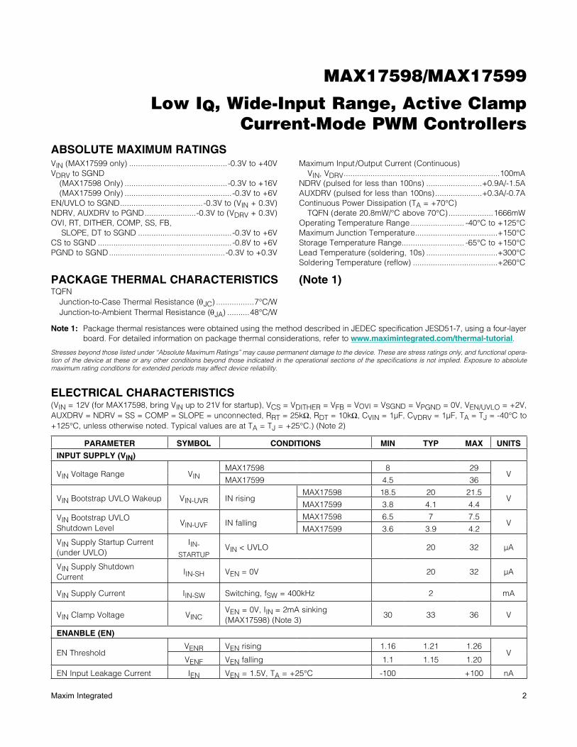
ABSOLUTE MAXIMUM RATINGS
Note 1: Package thermal resistances were obtained using the method described in JEDEC specification JESD51-7, using a four-layer board. For detailed information on package thermal considerations, refer to www.maximintegrated.com/thermal-tutorial.
Stresses beyond those listed under “Absolute Maximum Ratings” may cause permanent damage to the device. These are stress ratings only, and functional opera-tion of the device at these or any other conditions beyond those indicated in the operational sections of the specifications is not implied. Exposure to absolute maximum rating conditions for extended periods may affect device reliability.
ELECTRICAL CHARACTERISTICS(VIN = 12V (for MAX17598, bring VIN up to 21V for startup), VCS = VDITHER = VFB = VOVI = VSGND = VPGND = 0V, VEN/UVLO = +2V, AUXDRV = NDRV = SS = COMP = SLOPE = unconnected, RRT = 25kI, RDT = 10kI, CVIN = 1FF, CVDRV = 1FF, TA = TJ = -40NC to +125NC, unless otherwise noted. Typical values are at TA = TJ = +25NC.) (Note 2)
VIN (MAX17599 only) ............................................-0.3V to +40VVDRV to SGND
(MAX17598 Only) ..............................................-0.3V to +16V(MAX17599 Only) ................................................-0.3V to +6V
EN/UVLO to SGND ..................................... -0.3V to (VIN + 0.3V)NDRV, AUXDRV to PGND .......................-0.3V to (VDRV + 0.3V)OVI, RT, DITHER, COMP, SS, FB,
SLOPE, DT to SGND ..........................................-0.3V to +6VCS to SGND ............................................................-0.8V to +6VPGND to SGND ....................................................-0.3V to +0.3V
Maximum Input /Output Current (Continuous)VIN, VDRV ......................................................................100mA
NDRV (pulsed for less than 100ns) .........................+0.9A/-1.5AAUXDRV (pulsed for less than 100ns) .....................+0.3A/-0.7AContinuous Power Dissipation (TA = +70NC) TQFN (derate 20.8mW/°C above 70°C) ....................1666mWOperating Temperature Range ........................ -40°C to +125°CMaximum Junction Temperature .....................................+150°CStorage Temperature Range ............................ -65°C to +150°C Lead Temperature (soldering, 10s) ................................+300°CSoldering Temperature (reflow) ......................................+260°C
TQFN Junction-to-Case Thermal Resistance (qJC) .................7°C/W Junction-to-Ambient Thermal Resistance (qJA) ..........48°C/W
PACKAGE THERMAL CHARACTERISTICS (Note 1)
PARAMETER SYMBOL CONDITIONS MIN TYP MAX UNITS
INPUT SUPPLY (VIN)
VIN Voltage Range VINMAX17598 8 29
VMAX17599 4.5 36
VIN Bootstrap UVLO Wakeup VIN-UVR IN risingMAX17598 18.5 20 21.5
VMAX17599 3.8 4.1 4.4
VIN Bootstrap UVLO Shutdown Level
VIN-UVF IN fallingMAX17598 6.5 7 7.5
VMAX17599 3.6 3.9 4.2
VIN Supply Startup Current (under UVLO)
IIN-STARTUP
VIN < UVLO 20 32 FA
VIN Supply Shutdown Current
IIN-SH VEN = 0V 20 32 FA
VIN Supply Current IIN-SW Switching, fSW = 400kHz
2 mA
VIN Clamp Voltage VINCVEN = 0V, IIN = 2mA sinking (MAX17598) (Note 3)
30 33 36 V
ENANBLE (EN)
EN ThresholdVENR VEN rising 1.16 1.21 1.26
VVENF VEN falling 1.1 1.15 1.20
EN Input Leakage Current IEN VEN = 1.5V, TA = +25NC -100 +100 nA

MAX17598/MAX17599
Low IQ, Wide-Input Range, Active Clamp Current-Mode PWM Controllers
3Maxim Integrated
ELECTRICAL CHARACTERISTICS (continued)(VIN = 12V (for MAX17598, bring VIN up to 21V for startup), VCS = VDITHER = VFB = VOVI = VSGND = VPGND = 0V, VEN/UVLO = +2V, AUXDRV = NDRV = SS = COMP = SLOPE = unconnected, RRT = 25kI, RDT = 10kI, CVIN = 1FF, CVDRV = 1FF, TA = TJ = -40NC to +125NC, unless otherwise noted. Typical values are at TA = TJ = +25NC.) (Note 2)
PARAMETER SYMBOL CONDITIONS MIN TYP MAX UNITS
INTERNAL LDO (VDRV)
VDRV Output Voltage Range VVDRV
8V < VIN < 15V and 0mA < IVDRV < 50mA (MAX17598)
7.1 7.4 7.7
V
6V < VIN < 15V and 0mA < IVDRV < 50mA (MAX17599)
4.7 4.9 5.1
VDRV Current Limit IVDRV-MAX 70 100 mA
VDRV Dropout VVDRV-DO VIN = 4.5V, IVDRV = 20mA (MAX17599) 4.2 V
OVERVOLTAGE PROTECTION (OVI)
OVI Overvoltage ThresholdVOVIR VOVI rising 1.16 1.21 1.26
VVOVIF VOVI falling 1.1 1.15 1.2
OVI Masking Delay tOVI-MD 2 Fs
OVI Input Leakage Current IOVI VOVI = 1V, TA = +25NC -100 +100 nA
OSCILLATOR (RT)
NDRV Switching Frequency Range
fSW 100 1000 kHz
NDRV Switching Frequency Accuracy
-8 +8 %
Maximum Duty Cycle DMAX fSW = 400KHz, RDT = 10kI 71 72.5 74 %
SYNCHRONIZATION (DITHER/SYNC)
Synchronization Logic-High Input
VIH-SYNC 3 V
Synchronization Pulse Width 50 ns
Synchronization Frequency Range
fSYNC 1.1 x fSW
1.3 x fSW
DITHERING RAMP GENERATOR (DITHER/SYNC)
Charging Current 45 50 55 FA
Discharging Current 43 50 57 FA
Ramp-High Trip Point 2 V
Ramp-Low Trip Point 0.4

MAX17598/MAX17599
Low IQ, Wide-Input Range, Active Clamp Current-Mode PWM Controllers
4Maxim Integrated
ELECTRICAL CHARACTERISTICS (continued)(VIN = 12V (for MAX17598, bring VIN up to 21V for startup), VCS = VDITHER = VFB = VOVI = VSGND = VPGND = 0V, VEN/UVLO = +2V, AUXDRV = NDRV = SS = COMP = SLOPE = unconnected, RRT = 25kI, RDT = 10kI, CVIN = 1FF, CVDRV = 1FF, TA = TJ = -40NC to +125NC, unless otherwise noted. Typical values are at TA = TJ = +25NC.) (Note 2)
PARAMETER SYMBOL CONDITIONS MIN TYP MAX UNITS
SOFT-START/SOFT-STOP (SS)
Soft-Start Charging Current ISSCH 9 10 11 FA
Soft-Stop Discharging Current
ISSDISCH 4.4 5 5.6 FA
SS Bias Voltage VSS 1.19 1.21 1.23 V
SS Discharge Threshold VSSDISCH Soft-stop completion 0.15 V
NDRV DRIVER (NDRV)
Pulldown Impedance RNDRV-N INDRV (sinking) = 100mA 1.37 3 I
Pullup Impedance RNDRV-P INDRV (sourcing) = 50mA 4.26 8.5 I
Peak Sink Current CNDRV = 10nF 1.5 A
Peak Source Current CNDRV = 10nF 0.9 A
Fall Time tNDRV-F CNDRV = 1nF 10 ns
Rise Time tNDRV-R CNDRV = 1nF 20 ns
AUXDRV DRIVER (AUXDRV)
Pulldown Impedance RAUXDRV-N IAUXDRV (sinking) = 100mA 3.35 7 I
Pullup Impedance RAUXDRV-P IAUXDRV (sourcing) = 50mA 9.78 19 I
Peak Sink Current CAUXDRV = 10nF 0.7 A
Peak Source Current CAUXDRV = 10nF 0.3 A
Fall Time tAUXDRV-F CAUXDRV = 1nF 16 ns
Rise Time tAUXDRV-R CAUXDRV = 1nF 32 ns
DEAD TIME (DT)
NDRV to AUXDRV Delay (Dead Time)
tDT
NDRV$ to AUXDRV$ RDT = 10kI 25
nsRDT = 100kI 250
AUXDRV# to NDRV#RDT = 10kI 25
RDT = 100kI 250
CURRENT-LIMIT COMPARATOR (CS)
Cycle-by-Cycle Peak-Current-Limit Threshold
VCS-PEAK 290 305 320 mV
Cycle-by-Cycle Runaway-Current-Limit Threshold
VCS-RUN 340 360 380 mV
Cycle-by-Cycle Reverse-Current-Limit Threshold
VCS-REV -122 -102 -82 mV

MAX17598/MAX17599
Low IQ, Wide-Input Range, Active Clamp Current-Mode PWM Controllers
5Maxim Integrated
ELECTRICAL CHARACTERISTICS (continued)(VIN = 12V (for MAX17598, bring VIN up to 21V for startup), VCS = VDITHER = VFB = VOVI = VSGND = VPGND = 0V, VEN/UVLO = +2V, AUXDRV = NDRV = SS = COMP = SLOPE = unconnected, RRT = 25kI, RDT = 10kI, CVIN = 1FF, CVDRV = 1FF, TA = TJ = -40NC to +125NC, unless otherwise noted. Typical values are at TA = TJ = +25NC.) (Note 2)
PARAMETER SYMBOL CONDITIONS MIN TYP MAX UNITS
Current-Sense Leading-Edge Blanking Time
tCS-BLANK From NDRV# edge 70 ns
Current-Sense-Blanking Time for Reverse-Current Limit
tCS-BLANK-Rev
From AUXDRV$ edge 70 ns
Propagation Delay from Comparator Input to NDRV
tPDCS
From CS rising (10mV overdrive) to NDRV falling (excluding leading-edge blanking)
40 ns
Number of Consecutive Peak-Current-Limit Events to HICCUP
NHICCUP-P 8 event
Number of Runaway Current-Limit Events to HICCUP
N-HICCUP-R 1 event
Overcurrent Hiccup Timeout 32,768 cycle
Minimum On-Time tON-MIN 90 130 170 ns
SLOPE COMPENSATION (SLOPE)
Slope Bias Current ISLOPE 9 10 11 FA
Slope Resistor Range RSLOPE 25 200 kI
Slope Compensation Ramp RSLOPE = 100kW 140 165 190 mV/Fs
Default Slope Compensation Ramp
VSLOPE < 0.2V or 4V < VSLOPE 50 mV/Fs
PWM COMPARATOR
Comparator Offset Voltage VPWM-OS VCOMP, when VCS = 0V 1.65 1.81 2 V
Current-Sense Gain ACS-PWM DVCOMP /DVCS 1.75 1.97 2.15 V/V
Comparator Propagation Delay
tPWMChange in VCS = 10mV (including internal lead-edge blanking)
110 ns
ERROR AMPLIFIER
FB Reference Voltage VREFVFB, when ICOMP = 0V and VCOMP = 1.8V
1.19 1.21 1.23 V
FB Input Bias Current IFB VFB = 1.5V, TA = +25NC -100 +100 nA
Open-Loop Voltage Gain AEAMP 90 dB
Transconductance Gm 1.5 1.8 2.1 mS
MAX17598/MAX17599
Low IQ, Wide-Input Range, Active Clamp Current-Mode PWM Controllers
6Maxim Integrated
ELECTRICAL CHARACTERISTICS (continued)(VIN = 12V (for MAX17598, bring VIN up to 21V for startup), VCS = VDITHER = VFB = VOVI = VSGND = VPGND = 0V, VEN/UVLO = +2V, AUXDRV = NDRV = SS = COMP = SLOPE = unconnected, RRT = 25kI, RDT = 10kI, CVIN = 1FF, CVDRV = 1FF, TA = TJ = -40NC to +125NC, unless otherwise noted. Typical values are at TA = TJ = +25NC.) (Note 2)
Note 2: All devices are 100% production tested at +25NC. Limits over temperature are guaranteed by design.Note 3: The MAX17598 is intended for use in universal input power supplies. The internal clamp circuit at IN is used to prevent the
bootstrap capacitor from charging to a voltage beyond the absolute maximum rating of the device when EN is low (shut-down mode). Externally limit the maximum current to IN (hence to clamp) to 2mA (max) when EN is low.
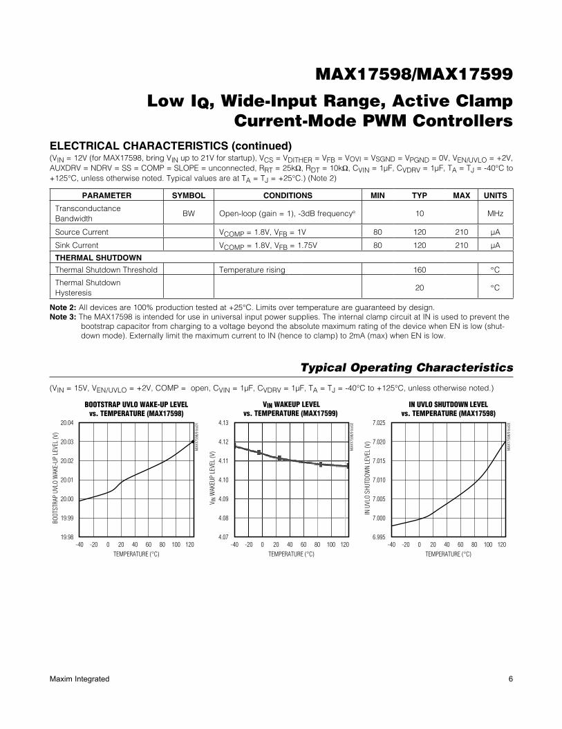
Typical Operating Characteristics
(VIN = 15V, VEN/UVLO = +2V, COMP = open, CVIN = 1FF, CVDRV = 1FF, TA = TJ = -40NC to +125NC, unless otherwise noted.)
PARAMETER SYMBOL CONDITIONS MIN TYP MAX UNITS
Transconductance Bandwidth
BW Open-loop (gain = 1), -3dB frequency° 10 MHz
Source Current VCOMP = 1.8V, VFB = 1V 80 120 210 FA
Sink Current VCOMP = 1.8V, VFB = 1.75V 80 120 210 FA
THERMAL SHUTDOWN
Thermal Shutdown Threshold Temperature rising 160 °C
Thermal Shutdown Hysteresis
20 °C
BOOTSTRAP UVLO WAKE-UP LEVELvs. TEMPERATURE (MAX17598)
MAX
1759
8/9
toc0
1
TEMPERATURE (°C)
BOOT
STRA
P UV
LO W
AKE-
UP L
EVEL
(V)
100806040200-20
19.99
20.00
20.01
20.02
20.03
20.04
19.98-40 120
VIN WAKEUP LEVELvs. TEMPERATURE (MAX17599)
MAX
1759
8/9
toc0
2
TEMPERATURE (°C)
V IN
WAK
EUP
LEVE
L (V
)
100806040200-20
4.09
4.08
4.10
4.11
4.12
4.13
4.07-40 120
IN UVLO SHUTDOWN LEVELvs. TEMPERATURE (MAX17598)
MAX
1759
8/9
toc0
3
TEMPERATURE (°C)
IN U
VLO
SHUT
DOW
N LE
VEL
(V)
100806040200-20
7.000
7.005
7.010
7.015
7.020
7.025
6.995-40 120

MAX17598/MAX17599
Low IQ, Wide-Input Range, Active Clamp Current-Mode PWM Controllers
7Maxim Integrated
Typical Operating Characteristics (continued)
(VIN = 15V, VEN/UVLO = +2V, COMP = open, CVIN = 1FF, CVDRV = 1FF, TA = TJ = -40NC to +125NC, unless otherwise noted.)
NDRV SWITCHING FREQUENCYvs. TEMPERATURE
MAX
1759
8/9
toc0
7
TEMPERATURE (°C)
NDRV
SW
ITCH
ING
FREQ
UENC
Y (k
Hz)
1008040 600 20-20
150
250
450
350
550
650
750
850
950
50-40 120
RT = 10kI
RT = 100kI
FREQUENCY DITHERING vs. RDITHERM
AX17
598/
9 to
c08
RDITHER (kI)
FREQ
UENC
Y DI
THER
ING
(%)
900800700600500400300
4
6
8
10
12
14
2200 1000
DEAD TIME vs. RDT
MAX
1759
8/9
toc0
9
RDT (kI)
DEAD
TIM
E - D
T (n
s)
9080706050403020
60
100
140
180
220
2010 100
MAX
1759
8/9
toc1
0
TEMPERATURE (°C)
DEAD
TIM
E (n
s)
DEAD TIME vs. TEMPERATURE
244
246
248
250
252
242120100806040200-20-40
RDT = 100kI
PEAK-CURRENT-LIMIT THRESHOLDvs. TEMPERATURE
MAX
1759
8/9
toc1
1
TEMPERATURE (°C)
PEAK
-CUR
RENT
-LIM
IT T
HRES
HOLD
(mV)
100 120806040200-20
301
302
303
304
305
306
307
300-40
REVERSE CURRENT LIMIT THRESHOLDvs. TEMPERATURE
MAX
1759
8/9
toc1
2
TEMPERATURE (°C)
REVE
RSE
CURR
ENT
LIM
IT T
HRES
HOLD
(mV)
12010060 800 20 40-20
-103
-102
-101
-100
-99
-98
-97
-96
-95
-104-40
VIN FALLING THRESHOLD vs.TEMPERATURE (MAX17599)
MAX
1759
8/9
toc0
4
TEMPERATURE (°C)
V IN
FALL
ING
THRE
SHOL
D (V
)
100806040200-20
3.88
3.89
3.90
3.91
3.92
3.87-40 120
IN SUPPLY CURRENT UNDER UVLOvs. TEMPERATURE
MAX
1759
8/9
toc0
5
TEMPERATURE (°C)
IN S
UPPL
Y CU
RREN
T UN
DER
UVLO
(µA)
100806040200-20
20.5
21.5
22.5
23.5
24.5
25.5
19.5-40 120
NDRV SWITCHING FREQUENCYvs. RESISTOR
MAX
1759
8/9
toc0
6
FREQUENCY SELECTION RESISTOR (kI)
NDRV
SW
ITCH
ING
FREQ
UENC
Y (k
Hz)
958565 7525 35 45 5515
100
200
300
400
500
600
700
800
900
1000
05

MAX17598/MAX17599
Low IQ, Wide-Input Range, Active Clamp Current-Mode PWM Controllers
8Maxim Integrated
Typical Operating Characteristics (continued)
(VIN = 15V, VEN/UVLO = +2V, COMP = open, CVIN = 1FF, CVDRV = 1FF, TA = TJ = -40NC to +125NC, unless otherwise noted.)
CURRENT-SENSE GAINvs. TEMPERATURE
MAX
1759
8/9
toc1
3
TEMPERATURE (°C)
CURR
ENT-
SENS
E GA
IN (V
/V)
100 120806040200-20
1.93
1.94
1.95
1.96
1.97
1.98
1.99
1.92-40
FB REGULATION VOLTAGEvs. TEMPERATURE
MAX
1759
8/9
toc1
4
TEMPERATURE (°C)
FB R
EGUL
ATIO
N VO
LTAG
E (V
)
100806040200-20
1.207
1.209
1.211
1.213
1.215
1.217
1.205-40 120
NDRV PEAK SOURCE ANDSINK CURRENTS
MAX17598/9 toc15
INDRV0.7A/div
200ns/div
PEAK SINKCURRENT
PEAK SOURCECURRENT
AUXDRV PEAK SOURCE ANDSINK CURRENTS
MAX17598/9 toc16
IAUXDRV0.28A/div
200ns/div
PEAK SINKCURRENT
PEAK SOURCECURRENT
MAX17598/MAX17599
Low IQ, Wide-Input Range, Active Clamp Current-Mode PWM Controllers
9Maxim Integrated
Typical Operating Characteristics (continued)
SOFT-START FROM INPUT (FIGURE 9)MAX17598/9 toc19
VIN20V/div
VOUT2V/div
200ms/div
NDRV AND AUXDRV SIGNALS (FIGURE 9)MAX17598/9 toc21
1µs/div
VNDRV5V/div
VAUXDRV5V/div
INPUT SHUTDOWN (FIGURE 9)MAX17598/9 toc20
20ms/div
VIN20V/div
VOUT2V/div
DEAD TIME BETWEEN NDRVAND AUXDRV (FIGURE 9)
MAX17598/9 toc22
40ns/div
VNDRV5V/div
VAUXDRV5V/div
50ns
ENABLE STARTUP WAVEFORM(DUTY-CYCLE SOFT-START)
MAX17598/9 toc17
VEN/UVLO2V/div
VOUT2V/div
4ms/div
ENABLE SHUTDOWN WAVEFORM(SOFT-STOP)
MAX17598/9 toc18
4ms/div
VEN/UVLO2V/div
VOUT2V/div

MAX17598/MAX17599
Low IQ, Wide-Input Range, Active Clamp Current-Mode PWM Controllers
10Maxim Integrated
Typical Operating Characteristics (continued)
LOAD TRANSIENT RESPONSE (FIGURE 9)MAX17598/9 toc25
ILOAD2A/div
VOUT (AC)100mV/div
200µs/div
EFFICIENCY CURVES
OUTPUT CURRENT (A)
EFFI
CIEN
CY (%
)
8642
15
20
30
40
50
60
70
80
90
100
00 10
VIN = 36VVIN = 48VVIN = 72V
MAX
1759
8/9
toc2
6
BODE PLOT (FIGURE 9)MAX17598/98 toc27
GAIN10dB/div
PHASE36°/div
BANDWIDTH = 10.3kHzPHASE MARGIN = 72°
6 8 1 2 24 46 68 81 1
ACTIVE CLAMP SWITCHINGWAVEFORM (FIGURE 9)
MAX17598/9 toc28
IPRIMARY1A/div
VDS50V/div
1µs/div
SS, NDRV AND AUXDRV INHICCUP MODE (FIGURE 9)
MAX17598/9 toc23
VNDRV5V/div
VAUXDRV5V/div
VSS500mV/div
4ms/div
MOMENTARY OVIOPERATION (FIGURE 9)
MAX17598/9 toc24
VSS1V/div
VOUT5V/div
VCLAMPCAP50V/div
VOVI5V/div
4ms/div

MAX17598/MAX17599
Low IQ, Wide-Input Range, Active Clamp Current-Mode PWM Controllers
11Maxim Integrated
Pin Description
Pin Configuration
PIN NAME FUNCTION
1 DTDead-Time Programming Resistor Connection. Connect resistor from DT to GND to set the desired dead time between the NDRV and AUXDRV signals. See the Dead Time section to calculate the resistor value for a particular dead time.
2 SLOPESlope Compensation Programming Input. A resistor RSLOPE connected from SLOPE to SGND programs the amount of internal slope compensation. Shorting this pin to SGND sets a default slope compensation of 50mV/Fs.
3 RTSwitching Frequency Programming Resistor Connection. Connect resistor from RT to SGND to set the PWM switching frequency.
4 DITHER/SYNC
Frequency Dithering Programming or Synchronization Connection. For spread-spectrum frequency operation, connect a capacitor from DITHER to SGND and a resistor from DITHER to RT. To synchronize the internal oscillator to the externally applied frequency, connect DITHER/SYNC to the synchronization pulse.
5 COMPTransconductance Amplifier Output. Connect the frequency compensation network between COMP and SGND in nonisolated applications and between COMP and FB pins in isolated applications.
6 FB Transconductance Error Amplifier Inverting Input
7 SSSoft-Start/Soft-Stop Capacitor Pin for Forward/Flyback Regulator. Connect a capacitor from SS to SGND to set the soft-start/soft-stop time interval.
8 SGND Signal Ground. Connect SGND to the signal ground plane.
9 CSCurrent-Sense Input. Current-sense connection for average current-sense and cycle-by-cycle current limit. Peak current limit trip voltage is 350mV (typ).
10 PGND Power Ground. Connect PGND to the power ground plane.
15
16
14
13
5
6
7
RT
DITH
ER/
SYNC
8
DT
PGND
CSAUXD
RV
1 3
VIN
4
12 10 9
EN/UVLO
OVI
SGND
SS
FB
COMPSL
OPE
NDRV
2
11
VDRV
EP
TQFN
MAX17598MAX17599
TOP VIEW
+

MAX17598/MAX17599
Low IQ, Wide-Input Range, Active Clamp Current-Mode PWM Controllers
12Maxim Integrated
Pin Description (continued)
Detailed Description
The MAX17598/MAX17599 low IQ active-clamp current-mode PWM controllers contain all the control circuitry required for design of wide-input isolated/nonisolated for-ward converter industrial power supplies. The MAX17598 has a rising UVLO threshold of 20V with a 13V hysteresis, and is therefore well-suited for universal input (rectified 85V AC to 265V AC) or telecom (36V DC to 72V DC) power supplies. The MAX17599 features a 4.1V rising UVLO with a 200mV hysteresis and is optimized for low-voltage industrial supplies (4.5V DC to 36V DC).
The devices include an AUX driver that drives an auxiliary MOSFET (clamp switch) that helps implement the active-clamp transformer reset topology for forward converters. Such a reset topology has several advantages, including reduced voltage stress on the switches, transformer size reduction due to larger allowable flux swing, and improved efficiency due to elimination of dissipative snubber circuit-ry. Programmable dead time between the AUX and main driver allows for zero voltage switching (ZVS).
Input Voltage RangeThe MAX17598 has different rising and falling undervolt-age lockout (UVLO) thresholds on the VIN pin than those of the MAX17599. The thresholds for the MAX17598 are optimized for implementing power-supply startup schemes typically used for off-line AC/DC and telecom DC-DC power supplies that are typically encountered in industrial applications. As such, the MAX17598 has no limitation on the maximum input voltage, as long as the external components are rated suitably, and the maxi-mum operating voltages of the MAX17598 are respected. The MAX17598 can be successfully used in universal input (85V to 265V AC) rectified bus applications, recti-fied 3-phase DC bus applications, and telecom (36V to 72V DC) applications.
The VIN pin of the MAX17599 has a maximum operating voltage of 36V. The MAX17599 implements rising and falling thresholds on the VIN pin that assume power-supply startup schemes, typical of lower voltage DC-DC applications down to an input voltage of 4.5V DC. Thus isolated/non-isolated active-clamp converters with sup-ply-voltage range of 4.5V to 36V can be implemented with the MAX17599. See Startup Operation section for more details on power-supply startup schemes for MAX17598/MAX17599.
PIN NAME FUNCTION
11 NDRV External Switching NMOS Gate-Driver Output
12 AUXDRVPMOS Active-Clamp-Switch Gate-Driver Output. AUXDRV can also be used to drive a pulse transformer for synchronous flyback application.
13 VDRVLinear Regulator Output and Driver Input. Connect a 1FF bypass capacitor from VDRV to PGND as close as possible to the IC.
14 VINInternal VDRV Regulator Input. Connect VIN to the input voltage source. Bypass VIN to PGND with a 0.1FF minimum ceramic capacitor.
15 EN/UVLOEnable/Undervoltage Lockout Pin. To externally program the UVLO threshold of the input supply, connect a resistive divider among input supply, EN/UVLO, and SGND.
16 OVIOvervoltage Comparator Input. Connect a resistive divider among the input supply, OVI, and SGND to set the input overvoltage threshold.
— EP Exposed Pad

MAX17598/MAX17599
Low IQ, Wide-Input Range, Active Clamp Current-Mode PWM Controllers
13Maxim Integrated
Figure 1. Block Diagram
CHIPEN/HICCUP
POK
EN/UVLO
OVI
RT
SS
SS
SS
1.21V
2V/0.4V
VIN
UVLO
TSDN
1.21V
1.21V
-102mV
305mV
360mV
SSDONE
HICCUP
VDRV
OSC
DITHER/SYNC
CLK
0.9V
CLK
DITHER/SYNC
LDO
THERMAL SENSOR
CHIPEN
SSDONE
CONTROL ANDDRIVER LOGIC
DT
VDRV
PGND
VDRV
PGND
DRIVER
DRIVER
7.4V (MAX17598)OR4.9V (MAX17599)
Q50µA
5µA
10µA
10µA
8 PEAKEVENTSOR 1 RUNAWAY
1.21V
REVERSE ILIMCOMP
PEAKLIMCOMP
RUNAWAYCOMP
PWMCOMP 70ns
BLANKING
SLOPEDECODE
CURRENTSOFT-START
FIXED ORVARIABLE
R
R
1x
MAX17598MAX17599
AUXDRV
NDRV
DEAD TIME
AUXDRV
NDRV
CS
SLOPE
COMP
FB
SGND
PGND
CHIPEN

MAX17598/MAX17599
Low IQ, Wide-Input Range, Active Clamp Current-Mode PWM Controllers
14Maxim Integrated
Figure 2. Programming EN/UVLO, OVI
Linear Regulator (VDRV)The MAX17598/MAX17599 have an internal linear regu-lator that is powered from the VIN pin. The output of the linear regulator is connected to the VDRV pin, and should be decoupled with a 1FF capacitor to ground for stable operation. The VDRV converter output sup-plies the MOSFET drivers internal to the MAX17598/MAX17599. The VDRV voltage is regulated at 7.4V (typ) in the MAX17598, and at 4.9V (typ) in the MAX17599. The maximum operating voltage of the IN pin is 29V for the MAX17598 and 36V for the MAX17599.
Maximum Duty Cycle (Dmax)The MAX17598/MAX17599 operate at a maximum duty cycle of 72.5% (typ). When the SLOPE pin is left OPEN, the ICs have the necessary amount of slope compensa-tion to provide stable, jitter-free current-mode control operation in applications where the operating duty cycle is less than 50%. Slope compensation is necessary for stable operation of current-mode controlled converters at duty cycles greater than 50%, in addition to the loop compensation required for small signal stability. The MAX17598/MAX17599 implement a SLOPE pin for this purpose. See the Slope Compensation Programming section for more details.
Applications Information
Startup Voltage and Input Overvoltage Protection Setting (EN/UVLO, OVI)
The EN/UVLO pin in the MAX17598/MAX17599 serves as an enable/disable input, as well as an accurate programmable undervoltage lockout (UVLO) pin. The MAX17598/MAX17599 do not commence startup opera-tions unless the EN/UVLO pin voltage exceeds 1.21V (typ). The MAX17598/MAX17599 turn off if the EN/UVLO pin voltage falls below 1.15V (typ). A resistor divider from the input DC bus to ground maybe used to divide down and apply a fraction of the input DC voltage to the EN/UVLO pin as shown in Figure 2. The values of the resistor divider can be selected so that the EN/UVLO pin voltage exceeds the 1.21V (typ) turn on threshold at the desired input DC bus voltage. The same resistor divider can be modified with an additional resistor, ROVI, to implement input overvoltage protection, in addition to the EN/UVLO functionality as shown in Figure 2. When the voltage at the OVI pin exceeds 1.21V (typ), the MAX17598/MAX17599 stop switching. Switching resumes with soft-start opera-
tion, only if the voltage at the OVI pin falls below 1.15V (typ). The OVI feature is easily disabled by tying the pin to ground. For given values of startup DC input voltage (VSTART) and input overvoltage protection voltage (VOVI), the resistor values for the divider can be calculated as follows, assuming a 24.9kI resistor for ROVI. RSUM rep-resents the series combination of several resistors that might be needed in high-voltage DC bus applications (MAX17598) or a single resistor in low-voltage DC-DC applications (MAX17599).
OVIEN
START
VR 24.9 1 k ,
V
= × − W
where VSTART and VOVI are in volts.
[ ] STARTSUM EN
VR 24.9 R 1 k ,
1.21 = + × − W
where REN is in kI. RSUM might need to be implemented as equal multiple resistors in series (RDC1, RDC2, RDC3) so that voltage across each resistor is limited to its maxi-mum operating voltage.
= = = WSUMDC1 DC2 DC3
RR R R k .
3
MAX17598MAX17599
RDC1
RDC2
RDC3
RSUM
EN/UVLO
OVI
REN
ROVI
VDC

MAX17598/MAX17599
Low IQ, Wide-Input Range, Active Clamp Current-Mode PWM Controllers
15Maxim Integrated
Startup OperationThe MAX17598 is optimized for implementing active-clamp converters operating either from a rectified AC input or in a 36V DC to 72VDC telecom application. A cost-effective RC startup circuit can be used in such applications. In this startup method (Figure 3), when the input DC voltage is applied, the startup resistor RSTART charges the startup capacitor CSTART, causing the voltage at the VIN pin to increase towards the rising VIN UVLO threshold (20V typical). During this time, the MAX17598 draws a low startup current of 20FA (typ) through the startup resistor RSTART. When the voltage at VIN reaches the rising IN UVLO threshold, the MAX17598 commences all internal operations and drives the exter-nal MOSFETs connected to NDRV and AUXDRV. In this condition, the MAX17598 draws 2mA (typ) current in from CSTART, in addition to the current required to switch the gates of the external MOSFETs Q1and Q2. Since this current cannot be supported by the current through RSTART, the voltage on CSTART starts to drop. When suitably configured as shown in Figure 3, the converter operates to generate an output voltage (VBIAS) that is bootstrapped to the VIN pin. If the voltage VBIAS exceeds 7V before the voltage on CSTART falls below 7V (typ), then the VIN voltage is sustained by VBIAS, thus allow-ing the MAX17598 to continue to operate with energy from VBIAS. The large hysteresis (13V typical) of the MAX17598 allows for a small startup capacitor (CSTART). The low startup current (20FA typical) allows the use of a large startup resistor (RSTART), thus reducing power dissipation at higher DC bus voltages. The startup resis-
tor RSTART might need to be implemented as equal, mul-tiple resistors in series (RIN1, RIN2 and RIN3) to share the applied high DC voltage in offline applications so that the voltage across each resistor is limited to the maximum continuous operating voltage rating. RSTART and CSTART can be calculated as follows:
× + × × = × + +
VDRV IN SS
START GATE swIN SS6
7.4 C 0.04 I C
C 0.09 µFQ fI t
10
where IIN is the supply current drawn at the IN pin in mA, QGATE is the sum of the gate charges of the exter-nal MOSFETs Q1 and Q2 in nC, fsw is the switching frequency of the converter in Hz, tSS is the soft-start time programmed for the converter in ms. CVDRV is cummulative capacitor used at DRV node in μF, and CSS is soft-start capacitor in nF. See the Soft-Start section.
( )STARTSTART
START
V 10 50R k ,
1 C
− ×= W
+
where CSTART is the startup capacitor in FF.
The IN UVLO rising threshold of the MAX17599 is set to 4.1V with a hysteresis of 200mV, and is optimized for low-voltage DC-DC applications in the range of 4.5V DC to 36V DC. The IN pin is rated for a maximum operating input voltage of 36V DC and can directly be connected to the input DC supply.
Figure 3. RC-Based Startup Circuit
RIN1
RIN2
RIN3
LDOVIN
VDC VBIAS
D1
D2
LBIAS
CCLAMP
VDC
AUXDRV
NDRV
Q1
Q2
VDRV
CVDRV
CSTART
RSTART
MAX17598

MAX17598/MAX17599
Low IQ, Wide-Input Range, Active Clamp Current-Mode PWM Controllers
16Maxim Integrated
Soft-Start and Soft-StopIn a current-mode isolated active clamp forward con-verter, the COMP voltage programs the peak current in the primary, and thus the secondary-side inductor current as well. The MAX17598/MAX17599 implement a soft-start scheme that controls the COMP pin of the device at turn on. A useful benefit of this feature is the elimination of need for secondary-side soft-start circuitry in such isolated applications. In the absence of sec-ondary-side soft-start circuitry, the secondary-side error amplifier can cause the output voltage to rapidly reach the regulation value, thus causing inrush current and output voltage overshoot. The MAX17598/MAX17599 avoid this issue by applying a soft-start to the COMP pin. Thus the regulator’s primary and secondary currents are ramped up in a well-controlled manner resulting in a current-mode soft-start operation.
Soft-start period of MAX17598/MAX17599 can be pro-grammed by selecting the value of capacitor connected from SS pin to GND. The capacitor CSS can be calcu-lated as follows:
×=
−SS
SSCOMP
10 tC nF
V 1.81
where tSS is in ms, VCOMP is steady-state COMP voltage (VCOMP,MAX = 2.6V).
A soft-stop feature ramps down the output voltage when the device is turned off, and provides safe discharging of the clamp capacitor, thus allowing the controller to restart in a well-controlled manner. Additionally, a nega-tive current limit is provided in the current-sense circuitry that helps limit the clamp switch current under dynamic operating conditions, such as momentary input overvolt-age charging from a precharged output capacitor. The soft-stop duration is twice that of the programmed soft-start period.
Programming Slope CompensationSince the MAX17598/MAX17599 operate at a maximum duty cycle of 72.5% (typ), slope compensation is required to prevent subharmonic instability that occurs naturally in continuous-conduction mode, peak current mode-controlled converters operating at duty cycles greater than 50%. A minimum amount of slope signal is added to the sensed current signal, even for converters operating below 50% duty to provide stable, jitter-free operation. The SLOPE pin allows the user to program the necessary slope compensation by setting the value of the resistor RSLOPE connected from SLOPE pin to ground.
ESLOPE
S 8R k
1.55−
= W
where SE, the slope is expressed in mV per microseconds.
For the default minimum slope compensation of 50mV/Fs (typ), the SLOPE pin should be connected to SGND or left unconnected.
Figure 4. Typical Startup Circuit with IN Connected Directly to DC Input
MAX17599
LDOVIN
4.5V TO 36V DC
VOUT
D1
D2
LOUT
CCLAMP
AUXDRV
NDRV
Q1
VDRV
CVDRV
COUT
Q2
MAX17598/MAX17599
Low IQ, Wide-Input Range, Active Clamp Current-Mode PWM Controllers
17Maxim Integrated
Figure 5. Duty Cycle Soft-Start
Figure 6. Duty Cycle or Current Soft-Stop
*VCOMP is steady-state COMP voltage.
AUXDRV
CS
SOFT-START BEGIN
0.0V0.4V
NDRV
VSS = ISSCH x t /CSSVCOMP* - 1.36V
SOFT-START ENDS
SOFT-STOP ENDS
0.4V
0.0V
VCOMP* - 1.36V
SOFT-STOP BEGINS
VSS = 1.21V - ISSDISCH x t /CSS
AUXDRV
CS
NDRV

MAX17598/MAX17599
Low IQ, Wide-Input Range, Active Clamp Current-Mode PWM Controllers
18Maxim Integrated
n-Channel MOSFET Gate DriverThe NDRV output drives an external n-channel MOSFET. NDRV can source/sink in excess of 900mA/1500mA peak current. Therefore, select a MOSFET that yields acceptable conduction and switching losses.
p-Channel MOSFET Gate DriverThe AUXDRV output drives an external p-channel MOSFET with the aid of a level shifter, as shown in the Typical Application Circuits. AUXDRV can source/sink in excess of 300mA/700mA peak current. Therefore, select a MOSFET that yields acceptable conduction and switch-ing losses. The external PMOSFET used must be able to withstand the maximum clamp voltage.
Dead TimeDead time between the main and AUX output edges allow ZVS to occur, minimizing switching losses and improving efficiency. The dead time (tDT) is applied to both leading and trailing edges of the main and AUX outputs as shown in Figure 7. Connect a resistor between DT and GND to set tDT to any value between 25ns and 250ns. RDT in kΩ, is calculated as:
= × WDT DTR 0.4 t k ,where tDT is in ns.
Oscillator/Switching FrequencyThe ICs’ switching frequency is programmable between 100kHz and 1MHz with a resistor RRT connected between RT and GND. Use the following formula to determine the appropriate value of RRT needed to generate the desired output switching frequency (fSW):
10
RTSW
1 10R
f×
=
where fSW is the desired switching frequency.
Peak-Current-LimitThe current-sense resistor (RCS), connected between the source of the n-channel MOSFET and PGND, sets the current limit. The source end of current-sense resistor connects to CS pin of MAX17598/MAX17599. The signal thus obtained is used by the devices, both for current-mode control and peak-current limiting purposes. The current-limit comparator has a voltage trip level (VCS-PEAK) of 305mV, and is independent of slope
compensation applied to stabilize the converter. The following equation is used to calculate the value of RCS:
=×CS
PRI_PEAK
305mVR
1.2 I
where IPRI_PEAK is the peak current in the primary side of the transformer, which also flows through the main n-channel MOSFET. When the voltage produced by this current (through the current-sense resistor) exceeds the current-limit comparator threshold, the MOSFET driver (NDRV) terminates the current on-cycle within 40ns (typ).
The devices implement 70ns of internal leading-edge blanking to ignore leading-edge current spikes encoun-tered in practice due to parasitics. Use a small RC network for additional filtering of the leading-edge spike on the sense waveform when needed. Set the corner frequency of the RC filter network at 5 to 10 times the switching frequency.
For a given peak-current-limit setting, the runaway cur-rent limit is typically 20% higher. The peak current-limit-triggered hiccup operation is disabled until the end of soft-start, while the runaway current-limit-triggered hiccup operation is always enabled.
Negative Peak Current LimitThe MAX17598/MAX17599 protect against excessive negative currents through the clamp switch, primary of the transformer and the clamp capacitor under dynamic operating conditions. The devices limit negative current by monitoring the voltage across RCS, while the AUXDRV output is low and the p-Channel FET is on. The typical negative-current-limit threshold is set at -102mV (1/3 of the positive-peak-current-limit threshold).
Figure 7. Dead Time Between AUXDRV and NDRV
AUXDRV
NDRV
DEAD TIME, tDT

MAX17598/MAX17599
Low IQ, Wide-Input Range, Active Clamp Current-Mode PWM Controllers
19Maxim Integrated
Output Short-Circuit Protection with Hiccup Mode
When the MAX17598/MAX17599 detect eight consecu-tive peak-current-limit events, both NDRV and AUXDRV driver outputs are turned off (hiccup is followed by soft-stop) for a restart period, tRSTR. After tRSTR, the device turns on again with a soft-start. The duration of the restart period is 32678 clock cycles, and therefore depends on the switching frequency setting. The device also features a runaway current limit setting at 120% (typ) of the peak current limit. This feature is useful under short-circuit faults in forward converters with synchronous rectifiers that occur during minimum on-time conditions at high input voltages. Under these conditions, the primary peak current tends to build up and staircase beyond the peak current limit setting due to insufficient discharging of the output inductor. One single event of a runaway current limit forces the MAX17598/MAX17599 into hiccup mode
operation. Figure 8 shows the behavior of the device prior and during hiccup mode.
Oscillator SynchronizationThe internal oscillator can be synchronized to an external clock by applying the clock to SYNC/DITHER directly. The external clock frequency can be set anywhere between 1.1x to 1.3x the internal clock frequency. Using an external clock increases the maximum duty cycle by a factor equal to fSYNC/fSW.
Frequency Dithering for Spread-Spectrum Applications (Low EMI)
The switching frequency of the converter can be dith-ered in a range of Q10% by connecting a capacitor from DITHER/SYNC to GND, and a resistor from DITHER to RT as shown in the Typical Applications Circuit. This results in lower EMI.
Figure 8. Hiccup-Mode Timing Diagram
CURRENT-SENSEVOLTAGE
HICCUP SIGNAL
SOFT-STARTVOLTAGE, VSS
VSS-HI
HICCUP TIMEOUT
tSS tRSTR
DISCHARGE WITHISSDISCH
VCS-PEAK(305mV)

MAX17598/MAX17599
Low IQ, Wide-Input Range, Active Clamp Current-Mode PWM Controllers
20Maxim Integrated
A current source at SYNC/DITHER charges the capacitor CDITHER to 2V with 50FA. Upon reaching this trip point, it discharges CDITHER to 0.4V with 50FA. The charging and discharging of the capacitor generates a triangular waveform on SYNC/DITHER with peak levels at 0.4V and 2V. CDITHER is calculated as:
=DITHERTRI
15.625C nF
f
where fTRI is in kHz.
Typically, fTRI should be set close to 1kHz. The resistor RDITHER connected from SYNC/DITHER to RT deter-mines the amount of dither as follows:
RT
DITHER
R%DITHER
R=
where %DITHER is the amount of dither expressed as a percentage of the switching frequency. Setting RDITHER to 10 x RRT generates Q10% dither.
Layout RecommendationsAll connections carrying pulsed currents must be very short and as wide as possible. The inductance of these connections must be kept to an absolute minimum due
to the high di/dt of the currents in high-frequency switch-ing power converters. This implies that the loop areas for forward- and return-pulsed currents in various parts of the circuit should be minimized. Additionally, small current loop areas reduce radiated EMI. Similarly, the heatsink of the MOSFET presents a dV/dt source. Therefore, the sur-face area of the MOSFET heatsink should be minimized as much as possible.
Ground planes must be kept as intact as possible. The ground plane for the power section of the converter should be kept separate from the analog ground plane, except for a connection at the least-noisy section of the power ground plane, typically the return of the input filter capacitor. The negative terminal of the filter capacitor, the ground return of the power switch, and current-sensing resistor must be close together. PCB layout also affects the thermal performance of the design. A number of thermal vias that connect to a large ground plane should be provided under the exposed pad of the part for efficient heat dissipation. For a sample layout that ensures first pass success, please refer to the MAX17598/MAX17599 Evaluation Kit layouts available at www.maximintegrated.com. For universal AC input designs, follow all applicable safety regulations. Offline power supplies can require UL, VDE, and other similar agency approvals.

MAX17598/MAX17599
Low IQ, Wide-Input Range, Active Clamp Current-Mode PWM Controllers
21Maxim Integrated
Typical Application Circuits
Figure 9. Typical Application Circuit (Telecom Power Supplies)
L21.5µH
L110mH
VOUT
VOUT
VOUT
PGND0
PGND0
VOUT
PGND0
3.3V, 8AOUTPUT
C547µF
C32.2µF
C222µF
C1022nF
C13OPEN
C142.2nF
C151000pF
C91µF
C180.47µF
C204.7µF
P1
N3
C110.047µF
C16100nF
N1NS
NP
NBD2
D1
N2
C4330µF
C74.7µF
C80.47µF
R1221kI
VIN
PGND
PGND
PGND
PGND
PGND
SGND
SGND
SGND
SGND
SGND
SGND
SGND
OVI
EN/UVLO
DITHER /SYNC
SGND
SGND
U2
U1
U313
2
VDRV
VDC
VFB
VFB
VDRV
T1
C647µF
R210R R3
10R
R90R
R120R
R20OPEN
R15OPEN
R1828.7kI
R610kI
R2349.9kI
R2422kI
R51.6MI
R735.7kI
R424.9kI
R1410kI
R820kI
R19100 R16
OPEN
R2230kI
R1149.9kI
R10221
R1310kI
R17470
3
2
1
4D4
D3
R210.1
VIN
VIN
VDC
PGND
INPUT
36V TO72V INPUT
C1100pF
C1933nF
C17OPEN
C12SHORT
(PC TRACE)
AUXDRV
NDRV
PGND
CS
DT
EP
VDRV
EN /UVLO
FB
COMP
SGND
RT
SLOPE
SS
DITHER/SYNC
OVI
MAX17598
PGND0

MAX17598/MAX17599
Low IQ, Wide-Input Range, Active Clamp Current-Mode PWM Controllers
22Maxim Integrated
Typical Application Circuits (continued)
Figure 10. Typical Application Circuit (Power Supply for Low-Voltage DC-DC Applications)
L110µH
VOUT
VOUT
GND0
GND0
VOUT
GND0
3.3V, 3AOUTPUT
C4100µF
C20.1µF
C122µF
C80.01µF
C1010nF
C1147pF
C124.7nF
C182.2µF
C72.2µF
C190.1µF
P1
N1
C60.47µF
C947nF
C1347nF
N3NSNP
NB
N2
C14100µF
C1647nF
VIN
PGND
PGND
PGND
PGND
PGND
SGNDSGND
SGND
SGND
SGND
OVI
EN/UVLO
SGND
SGND
U2
U1
U313
2VDRV
VDC
VFB
VFB
VDRV
T1
C15100µF
C5OPEN
R310R R2
10R
R100R
R120R
R11OPEN
R23OPEN
R1540kI
R1949.9kI
R2033.2kI
R13.3MI
R4150kI
R5121kI
C17SHORT
R610kI
R920kI
R16100R
R24100kI
R25150kI
R2147I
R1322kI
R18200kI
R8332kI
R7120I
R14470R
4
2
1
1
3 2
5
D1
R22100kI
R17100m
Z26.2V
Q1
D3
D2
VIN
VIN
PGND
INPUT
17V TO34V INPUT
C20100pF
AUXDRV
NDRV
PGND
CS
DT
EP
VDRV
EN /UVLO
FB
COMP
SGND
RT
SLOPE
SS
DITHER/SYNC
OVI
MAX17599
VDC
GND0

MAX17598/MAX17599
Low IQ, Wide-Input Range, Active Clamp Current-Mode PWM Controllers
23Maxim Integrated
Ordering Information
+Denotes a lead(Pb)-free/RoHS-compliant package.
Package Information
For the latest package outline information and land patterns (foot-prints), go to www.maximintegrated.com/packages. Note that a “+”, “#”, or “-” in the package code indicates RoHS status only. Package drawings may show a different suffix character, but the drawing pertains to the package regardless of RoHS status.
PART TEMP RANGE PIN PACKAGE FUNCTIONALITYUVLO, IN CLAMP
Dmax
MAX17598ATE+ -40NC to +125NC 16 TQFNActive-clamp, peak-current-mode, offline PWM controller
20V, Yes 70%
MAX17599ATE+ -40NC to +125NC 16 TQFNActive-clamp, peak-current-mode, PWM DC-DC controller
4V, No 70%
PACKAGE TYPE
PACKAGE CODE
OUTLINE NO.
LAND PATTERN NO.
16 TQFN T1633+4 21-0136 90-0032
MAX17598/MAX17599
Low IQ, Wide-Input Range, Active Clamp Current-Mode PWM Controllers
Maxim Integrated cannot assume responsibility for use of any circuitry other than circuitry entirely embodied in a Maxim Integrated product. No circuit patent licenses are implied. Maxim Integrated reserves the right to change the circuitry and specifications without notice at any time. The parametric values (min and max limits) shown in the Electrical Characteristics table are guaranteed. Other parametric values quoted in this data sheet are provided for guidance.
Maxim Integrated 160 Rio Robles, San Jose, CA 95134 USA 1-408-601-1000 24© 2014 Maxim Integrated Products, Inc. Maxim Integrated and the Maxim Integrated logo are trademarks of Maxim Integrated Products, Inc.
Revision History
REVISIONNUMBER
REVISIONDATE
DESCRIPTIONPAGES
CHANGED
0 1/12 Initial release —
1 3/13Updated General Description, Benefits and Features, Absolute Maximum Ratings, Electrical Characteristics, Typical Operating Characteristics, Pin Description, Detailed Description sections, and Figures 1, 3–6, 8–10
1–23
2 4/14 R2 and R3 components values updated. 21-22