Neuron, Volume 61 Supplemental Data Timing, timing, timing ...

Mathematical Modeling of Timing Attributes of Self-Timed
Carry Select Adders
P. BALASUBRAMANIAN*, C. JACOB PRATHAP RAJ1,§
, S. ANANDHI1,§
, U. BHAVANIDEVI1,†
,
N. E. MASTORAKIS#
* Department of Electronics and Communication Engineering
S. A. Engineering College (Affiliated to Anna University)
Poonamallee-Avadi Main Road, Veeraraghavapuram, Chennai 600 077
INDIA
QuEST Technosoft Solutions (I) Pvt. Ltd.
2nd
Floor, G. S. Plaza, Road No. 1, Banjara Hills, Hyderabad 500 034
INDIA
{jacobsaece, anandhisaece}@gmail.com † Cognizant Technology Solutions
5/535 Old Mahabalipuram Road, Okkiam Thoraipakkam, Chennai 600 097
INDIA
Division of Electrical Engineering and Computer Science
Military Institutions of University Education, Hellenic Naval Academy
Piraeus 18539
GREECE
Abstract: - A mathematical model to estimate the timing parameters of self-timed carry select adders (CSAs) is
described in this paper. This research builds upon our recent, earlier work in this domain dealing with timing
prediction of self-timed carry-ripple adders (CRAs). A comprehensive analysis is performed that compares the
timing attributes of self-timed CSAs and CRAs for addition widths ranging from 16 to 256 bits, for varying
lengths of the carry propagation chain. For ease of analysis, only uniform CSAs are considered in this work
although the mathematical model presented is generic and can be extended to address non-uniform length
CSAs as well. Strong, weak, and biased (weak) indicating types with respect to both self-timed CRAs and
CSAs have been considered for theoretical analysis, and simulation based information has been used to obtain
timing results based on the proposed mathematical model. The major inferences derived from this work are: i)
for normal carry chain lengths, self-timed CRAs are preferable over self-timed CSAs, and ii) as the length of
the carry propagation chain increases, self-timed CSAs assert growing supremacy over self-timed CRAs in
terms of speed for the case of regular and wide-operand adders.
Key-Words: - Self-timed design, Indication, Carry-ripple adder, Carry select adder, Latency, Cycle time.
1 This research was performed when the authors were affiliated with the Department of Electronics and
Communication Engineering, S. A. Engineering College, Chennai 600 077, India.
1 Introduction Self-timed design, that represents a robust flavor of
asynchronous digital design, is widely acclaimed as
a viable alternative to mainstream synchronous
design as they possess the inherent ability to cope
with process, temperature and parametric variations
[1] – [4], which tend to increase with continuous
shrinkage of device geometries [5]. Although there
have been many notable pursuits in the domain of
asynchronous digital design by both academia and
industry; a representative list of which includes [6] –
[19], this design method has not yet been widely
embraced because of the non-availability of a
substantial number of trained engineers and industry
experts. The reason for this is owing to the fact that
Recent Advances in Circuits, Systems, Telecommunications and Control
ISBN: 978-960-474-341-4 228

self-timed design styles are unorthodox and could
be way too different from conventional synchronous
design methods in cases. With the Semiconductor
Industry Association’s ITRS design reports [5]
forecasting an increasing dependency on
asynchronous logic in the coming decades, interest
in this design approach has been picking up and
some companies have been concentrating on pilot
projects [13] [20] [21] as a means of testing the
waters before venturing into large scale R&D
investment, design, development and commercial
release of asynchronous EDA tools. With this aim,
some companies have set up dedicated research
units focusing on asynchronous design tools
development – Sun Microsystems (now part of
Oracle America) [22] and Tanner EDA [23], for
example. In this context, it is to be noted that free
asynchronous tool offerings have already been made
available by academia for general use [24] – [26],
and some companies had made commercial exploits
in this arena – Philips [10], Fulcrum Microsystems,
now part of Intel [27], Camgian Microsystems,
formerly called Theseus Logic Inc. [28], Silistix Inc,
now a partner company of ARM [29] etc. Given
these, the purpose of this paper is to serve as an eye-
opener and a ready-reference to early stage
researchers and industry professionals by exposing
the intricacies of a robust class of asynchronous
(self-timed) design from the perspective of
arithmetic circuits – the discussion here centers
around self-timed CRAs and CSAs. The bottom-line
of this work is to show how the timing parameters
of a self-timed circuit can be theoretically analyzed
and predicted in the absence of a sophisticated EDA
tool to facilitate in-depth understanding.
The rest of this paper is organized as follows.
Section 2 introduces the basics of self-timed design.
Section 3 presents the mathematical equations
underlying strong, weak, and biased (weak)
implementation styles of self-timed CSAs with
reference to the corresponding mathematical
expressions of self-timed CRAs. Section 4 details
the comparison between self-timed CSAs and CRAs
on the basis of an important timing attribute viz.
cycle time, for different operand widths. This is
followed by the concluding remarks in Section 5.
2 Self-Timed Design – Basics The robustness attribute of self-timed design arises
from the fact that delay-insensitive codes are widely
used for data representation and processing. Among
the generic family of delay-insensitive m-of-n codes
[30], the dual-rail code is widely preferred owing to
its simplicity and ease of mapping with binary data.
On the basis of the double-rail code, a data wire x
is represented using 2 wires x1 and x0, where x1 = 1
and x0 = 0 signifies binary ‘1’, and x
0 = 1 and x
1 = 0
signifies binary ‘0’. x1 = x
0 = 0 represents spacer,
while x1 = x0 = 1 is invalid since the coding scheme
is unordered [31], i.e. no code word is permitted to
form a subset of another code word. Self-timed
designs normally encompass a delay-insensitive
coding scheme for data representation and a 4-phase
handshaking convention to control the data flow.
The 4-phase handshaking mechanism involves
return-to-zero signaling, which is explained below.
Fig. 1. Delay-insensitive data encoding and 4-phase
handshaking
• The dual-rail data bus is initially in the spacer
state. The sender transmits the codeword
(valid data). This results in 'low' to 'high'
transitions on the bus wires (i.e. any one of
the rails of all the dual-rail signals is assigned
a logic 'high' state), which correspond to non-
zero bits of the codeword
• After the receiver receives the codeword, it
drives the ackout (ackin) wire 'high' ('low')
• The sender waits for the ackin to go 'low' and
then resets the data bus (i.e. driven to spacer)
• After an unbounded, but finite (positive)
amount of time, the receiver drives the ackout
(ackin) wire 'low' ('high'). A single transaction
is now said to be complete and the system is
ready to commence the next transaction
In addition to a robust protocol governing data
flow in a self-timed system, the self-timed circuit
constituting the system tends to be indicating – here
indication means the circuit apart from having to
produce correct output(s) for the specified input(s)
is also endowed with the responsibility of duly
guaranteeing completion of computation at all the
internal nodes. There are two main indicating modes
defined for a self-timed system [32]: strong-
indication and weak-indication. Strongly indicating
circuits wait for all the primary inputs (valid data or
spacer) to arrive before starting computation to
Recent Advances in Circuits, Systems, Telecommunications and Control
ISBN: 978-960-474-341-4 229

produce the primary outputs, while weak-indication
circuits are allowed to produce the primary outputs
based on a subset of the primary inputs. However, at
least one output would be withheld until the arrival
of all the inputs is complete – this condition should
be satisfied for valid data and spacers. The timing
behavior of strong and weak-indication circuits is
portrayed through Fig. 2 for an illustration.
Outputs reset
Fig. 2. Depicting the mechanism of data processing
in strong and weak-indication circuits
Let us consider some examples for strong and
weak-indication types of self-timed adder modules,
as these will help to understand the circuit property
before proceeding with the comparative analysis of
different flavors of self-timed CRAs and CSAs.
2.1 Strongly Indicating Full Adder The strong-indication full adder synthesized using
DIMS method [33] is shown in Fig. 3. Here, (a1, a0),
(b1, b
0) and (cin
1, cin
0) signify the dual-rail encoded
inputs, while (Sum1, Sum
0) and (Cout
1, Cout
0)
represent the dual-rail encoded outputs. AND gate
symbol with the marking ‘C’ on their periphery in
Fig. 3 represents a C-element2. The equations
governing the strongly indicating full adder are,
Sum1 = a
0b
0cin
1 + a
0b
1cin
0 + a
1b
0cin
0 + a
1b
1cin
1 (1)
Sum0 = a0
b0cin
0 + a0b
1cin
1 + a1b
0cin
1 + a1b
1cin
0 (2)
2 The C-element governs the rendezvous of input
signals. It outputs a 1 (0) if all its inputs are 1 (0);
otherwise it maintains its existing state.
Cout1 = a
0b
1cin
1 + a
1b
0cin
1 + a
1b
1cin
0 + a
1b
1cin
1 (3)
Cout
0 = a0b
0cin
0 + a0b
0cin
1 + a0b
1cin
0 + a1b
0cin
0 (4)
It may be evident from Fig. 3 that the product
terms comprising (1) to (4) have been implemented
using C-elements, and because the products are
mutually disjoint [34] (i.e. their logical conjunction
results in a null), only one of the product terms is
asserted ‘high’ during a valid data phase. To
physically realize high fan-in C-elements, a safe
quasi-delay-insensitive decomposition approach has
to be followed, which is described in our earlier
work [35]. During a valid data phase, none of the
primary outputs will be produced until after the
requisite inputs have arrived. Similarly, set outputs
will be reset during the spacer phase only after all
the asserted inputs are driven to spacer state. Toms’
full adder [36] also belongs to this category;
however, it differs from the DIMS approach in that
it yields a decomposed synthesis solution.
Sum0
b0 C
C
C
C
C
C
C
C
Sum1
Cout0
Cout1
a0
cin0
b0a0
cin1
b1a0
cin0
b1a0
cin1
b0a1
cin0
b0a1
cin1
b1a1
cin0
b1a1
cin1
Fig. 3. DIMS strong-indication full adder
2.2 Weakly Indicating Full Adder Another variety of DIMS full adder [33] [37] that
belongs to weak-indication style is shown in Fig. 4.
The sum output equations are the same as given
earlier, while the carry outputs are given by,
Cout1 = a1
b1 + a1
b0cin
1 + a0b
1cin
1 (5)
Cout
0 = a0b
0 + a0b
1cin
0 + a1
b0cin
0 (6)
Recent Advances in Circuits, Systems, Telecommunications and Control
ISBN: 978-960-474-341-4 230
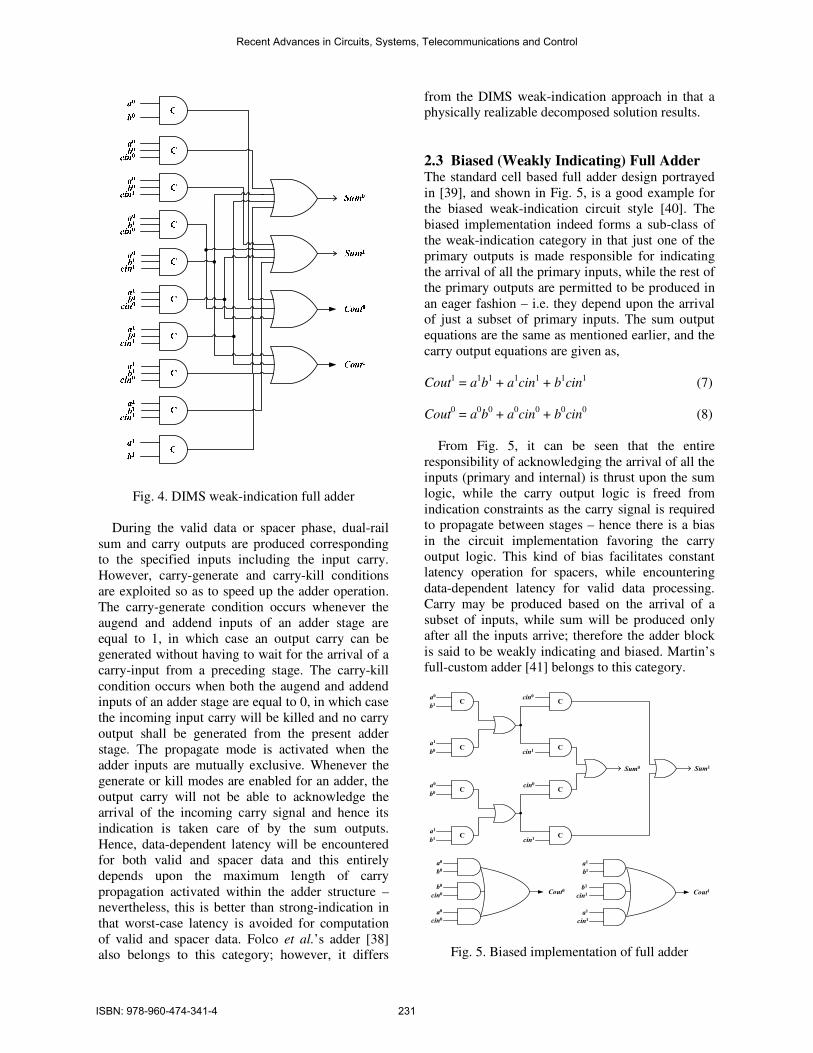
Fig. 4. DIMS weak-indication full adder
During the valid data or spacer phase, dual-rail
sum and carry outputs are produced corresponding
to the specified inputs including the input carry.
However, carry-generate and carry-kill conditions
are exploited so as to speed up the adder operation.
The carry-generate condition occurs whenever the
augend and addend inputs of an adder stage are
equal to 1, in which case an output carry can be
generated without having to wait for the arrival of a
carry-input from a preceding stage. The carry-kill
condition occurs when both the augend and addend
inputs of an adder stage are equal to 0, in which case
the incoming input carry will be killed and no carry
output shall be generated from the present adder
stage. The propagate mode is activated when the
adder inputs are mutually exclusive. Whenever the
generate or kill modes are enabled for an adder, the
output carry will not be able to acknowledge the
arrival of the incoming carry signal and hence its
indication is taken care of by the sum outputs.
Hence, data-dependent latency will be encountered
for both valid and spacer data and this entirely
depends upon the maximum length of carry
propagation activated within the adder structure –
nevertheless, this is better than strong-indication in
that worst-case latency is avoided for computation
of valid and spacer data. Folco et al.’s adder [38]
also belongs to this category; however, it differs
from the DIMS weak-indication approach in that a
physically realizable decomposed solution results.
2.3 Biased (Weakly Indicating) Full Adder The standard cell based full adder design portrayed
in [39], and shown in Fig. 5, is a good example for
the biased weak-indication circuit style [40]. The
biased implementation indeed forms a sub-class of
the weak-indication category in that just one of the
primary outputs is made responsible for indicating
the arrival of all the primary inputs, while the rest of
the primary outputs are permitted to be produced in
an eager fashion – i.e. they depend upon the arrival
of just a subset of primary inputs. The sum output
equations are the same as mentioned earlier, and the
carry output equations are given as,
Cout1 = a1
b1 + a1
cin1 + b1
cin1 (7)
Cout0 = a
0b
0 + a
0cin
0 + b
0cin
0 (8)
From Fig. 5, it can be seen that the entire
responsibility of acknowledging the arrival of all the
inputs (primary and internal) is thrust upon the sum
logic, while the carry output logic is freed from
indication constraints as the carry signal is required
to propagate between stages – hence there is a bias
in the circuit implementation favoring the carry
output logic. This kind of bias facilitates constant
latency operation for spacers, while encountering
data-dependent latency for valid data processing.
Carry may be produced based on the arrival of a
subset of inputs, while sum will be produced only
after all the inputs arrive; therefore the adder block
is said to be weakly indicating and biased. Martin’s
full-custom adder [41] belongs to this category.
C
C
a0
b1
a1
b0
C
C
cin0
cin1
C
C
a0
b0
a1
b1
C
C
cin0
cin1
Sum0 Sum1
a0
b0
b0
cin0
a0
cin0
a1
b1
b1
cin1
a1
cin1
Cout0 Cout1
Fig. 5. Biased implementation of full adder
Recent Advances in Circuits, Systems, Telecommunications and Control
ISBN: 978-960-474-341-4 231

3 Self-Timed Carry Select Adders In the synchronous world, carry-ripple adder is
labelled as a linear-time adder and hence not chosen
for high-performance applications. However, in the
realm of self-timed computer arithmetic, the CRA is
preferable because given a weakly indicating
realization (say, biased category), the CRA would
just encounter data-dependent ‘forward latency’ and
a constant ‘reverse latency’; hence less ‘cycle time’.
Forward latency refers to the computation time
taken for processing valid data, while reverse
latency is the time taken for resetting the circuit.
Cycle time is the sum of forward and reverse
latencies, and it is an indicator of the time taken to
complete a data transaction.
The issue of data-dependent latency arises from
an interesting study carried out in [42], where it was
found from a preliminary analysis that typical data
operations require a carry propagation chain length
of approximately 18 bits, while address calculations
resulted in a carry chain length of about 9 bits. The
average length of the carry chain exercised was
found to be around 12 to 13 bits, although this might
vary depending on specific operations performed.
In the synchronous domain, the carry select adder
is understood to be a high-speed logarithmic time
adder [43]. With respect to a self-timed realization,
the CSA is likely to be better than the CRA, more so
for lengthy carry propagation, especially in terms of
forward latency and eventually the cycle time; the
reverse latency metric of CRA will be slightly less
than the CSA as the latter will involve an extra
multiplexer (MUX) delay in addition to two full
adder delays of the former. This will be evident
from the forward and reverse timing characteristics
of CSA and CRA, highlighted using dotted arrows
in Fig. 6 – the architectures of a self-timed CSA and
CRA are depicted via Fig. 6 for the sample case of
8-bit addition operation. In Fig. 6, the 2:1 MUX
block refers to a 2:1 multiplexer – the function of a
multiplexer is to select a data input based on the
value of the select line(s) and transmit that value to
Recent Advances in Circuits, Systems, Telecommunications and Control
ISBN: 978-960-474-341-4 232

the output side. Assuming (a1, a
0), (b
1, b
0), (s
1, s
0) to
be the dual-rail encoded data and select inputs of a
2:1 MUX, and with (Y1, Y
0) representing the dual-
rail encoded output, the standard equations of the
dual-rail encoded 2:1 MUX are,
Y1 = a
1s
0 + b
1s
1 (9)
Y0 = a0s
0 + b0s
1 (10)
The detailed mathematical analysis of a self-
timed ripple-carry adder has been done in our recent
work [44]. By referring to this published literature,
the following sub-sections seek to compare and
contrast the respective timing attribute of uniform
length self-timed CSAs and CRAs under different
indicating modes.
3.1 CSA vs CRA Timing Comparison –
Strong-Indication Type
Let strong
FAT and MUXT represent the propagation
delay of a strongly indicating full adder (FA) and a
2:1 MUX element respectively, and let strong
CSACT _
denote the cycle time of a strongly indicating CSA.
With k and l signifying the size of the least
significant ripple-carry adder section of the CSA,
and the number of 2:1 MUX blocks present in the
critical path respectively, we have the following.
Here, the ripple-carry adder section implies a series
cascade of strongly indicating full adder blocks.
( )MUX
strong
FA
strong
CSAC TlTkT ×+×= 2_ (11)
By considering the cycle time expression of a
strongly indicating CRA [44], the extent of cycle
time reduction attainable by the CSA vis-à-vis the
CRA is given by (12), where n signifies adder size.
( ) ( )strong
FA
MUX
strong
FA
strong
FAstrong
CRTn
TlTkTnT
×
×+×−×=
2
22
(12)
3.2 CSA vs CRA Timing Comparison –
Weak-Indication Type
Let weak
FAT represent the propagation delay, and
weak
CSACT _ the cycle time of a weak-indication full
adder block and CSA respectively. The cycle time
of CSA is then expressed by (13). Since the carry
propagation chain lengths of CSA and CRA could
be similar or different, the cycle time metric for
CSA might be lesser or greater than the cycle time
encountered for a CRA. Hence, the potential
reduction in cycle time attainable by the CSA over
the CRA shall be given by (14) and the possible
cycle time reduction that may be achieved by the
latter over the former would be given by (15). Here,
p denotes the maximum length of carry propagation
in case of a CSA, while m stands for the maximum
carry propagation chain length of a CRA. It should
be noted that any of these scenarios might occur for
weak-indication in general: p < m, p > m and p = m.
( )MUX
weak
FA
weak
CSAC TlTpT ×+×= 2_ (13)
( ) ( )weak
FA
MUX
weak
FA
weak
FAweak
CSACRTm
TlTpTmT
×
×+×−×=
2
22_
(14)
( ) ( )( )MUX
weak
FA
weak
FAMUX
weak
FAweak
CRACRTlTp
TmTlTpT
×+×
×−×+×=
2
22_
(15)
Usage of (14) or (15) would be dependent on the
cycle time parameter as estimated for self-timed
CSA and CRA architectures.
3.3 CSA vs CRA Timing Comparison –
Biased (Weak-Indication) Type
Let biased
FAT denote the propagation delay of a biased
weak-indication full adder, and biased
CSACT _ the cycle
time of a biased weak-indication CSA. The cycle
time of CSA is then given by (16). Similar to the
discussion in the previous sub-section, depending on
the length of the carry propagation chain activated
in case of CSAs and CRAs, either of these adder
topologies may report less cycle time compared to
the other. Given this, the potential reduction in cycle
time achievable for the CSA in comparison with the
CRA shall be expressed by (17) and the reverse case
would be described by (18). As mentioned above,
the choice of (17) or (18) depends on the cycle time
parameter as estimated for the respective CSA and
CRA topologies.
MUX
biased
FA
biased
CSAC TlTpT ×+×+= 2)2(_ (16)
( ){ }biased
FA
MUX
biased
FA
biased
FAbiased
CSACRTm
TlTpTmT
×+
×+×+−×+=
)2(
22)2(_
(17)
Recent Advances in Circuits, Systems, Telecommunications and Control
ISBN: 978-960-474-341-4 233

( ){ }( ) MUX
biased
FA
biased
FAMUX
biased
FAbiased
CRACRTlTp
TmTlTpT
×+×+
×+−×+×+=
22
)2(22_
(18)
4 Results of Mathematical Analysis In order to estimate the extent of cycle time
reduction for self-timed CSAs over self-timed CRAs
and vice-versa, the corresponding equations have to
be simplified – this is made possible through the
mathematical substitution: FAMUX TT
32≅ , i.e. the
propagation delay of a 2:1 MUX is found to be
approximately equal to two-thirds of a full adder
delay – this is based on simulation data obtained.
The values of k, l, m, n and p are all user-defined.
Given these, the percentage reduction in cycle time
has been estimated with respect to strong, weak and
biased (weak) indication modes for a plethora of
adder sizes ranging from 16 to 256 bits and for
various lengths of the carry propagation chain – the
complete set of results is shown in the Appendix.
5 Conclusion Ripple carry adders, though signify a low-speed,
simple carry-propagate scheme in the synchronous
domain, represent a very useful and feasible option
with respect to self-timed design style. Since a
carry-ripple structure is inherent in a carry-select
adder topology, this work attempted a detailed
investigation of the timing attribute of self-timed
CSAs vis-à-vis self-timed CRAs to ascertain the
merits and de-merits of these two adder structures.
The mathematical modeling and the subsequent
results obtained for an extensive evaluation of
adders of various sizes and different carry chain
lengths drive home the following inferences: i) for a
strongly indicating implementation, self-timed
CSAs outperform self-timed CRAs by huge margins
in all cases, ii) for weak and biased-weak type
realizations, self-timed CRAs report better speed
than self-timed CSAs for nominal carry chain
lengths, while for lengthy carry propagation the
latter is preferable compared to the former.
References:
[1] A.J. Martin, S.M. Burns, T.K. Lee, D.
Borkovic, P.J. Hazewindus, “The first
asynchronous microprocessor: The test results,”
ACM SIGARCH Computer Architecture News,
vol. 17, no. 4, pp. 95-98, 1989.
[2] K.J. Kulikowski, V. Venkataraman, Z. Wang,
A. Taubin, M. Karpovsky, “Asynchronous
balanced gates tolerant to interconnect
variability,” Proc. IEEE International
Symposium on Circuits and Systems, pp. 3190-
3193, 2008.
[3] I.J. Chang, S.P. Park, K. Roy, “Exploring
asynchronous design techniques for process-
tolerant and energy-efficient subthreshold
operation,” IEEE Journal of Solid-State
Circuits, vol. 45, no. 2, pp. 401-410, 2010.
[4] J. Hamon, L. Fesquet, “Robust and
programmable self-timed ring oscillators,”
Proc. 9th
IEEE NEWCAS, pp. 249-252, 2011.
[5] International Technology Roadmap for
Semiconductors. Available: http://itrs.net
[6] S.B. Furber, P. Day, J.D. Garside, N.C. Paver,
J.V. Woods, “AMULET1: A micropipelined
ARM,” Digest of Papers, IEEE Computer
Society International Conference, pp. 476-485,
1994.
[7] T. Nanya, Y. Ueno, H. Kagotani, M. Kuwako,
A. Takamura, “TITAC: Design of a quasi-
delay-insensitive microprocessor,” IEEE
Design and Test of Computers, vol. 11, no. 2,
pp. 50-63, April 1994.
[8] A.J. Martin, A. Lines, R. Manohar, M.
Nystrom, P. Penzes, R. Southworth, U.
Cummings, “The design of an asynchronous
MIPS R3000 Processor,” Proc. 17th
Conference
on Advanced Research in VLSI, pp. 164-181,
1997.
[9] T. Nanya et al., “TITAC-2: A 32-bit scalable
delay-insensitive microprocessor,” Proc. HOT
Chips IX, pp. 19-32, 1997.
[10] H. van Gageldonk, K. van Berkel, Ad Peeters,
D. Baumann, D. Gloor, G. Stegmann, “An
asynchronous low power 80C51
microcontroller,” Proc. 4th International
Symposium on Advanced Research in
Asynchronous Circuits and Systems, pp. 96-
107, 1998.
[11] M. Renaudin, P. Vivet, F. Robin, “ASPRO-
216: A standard-cell QDI 16-bit RISC
asynchronous microprocessor,” Proc.
International Symposium on Advanced
Research in Asynchronous Circuits and
Systems, pp. 22-31, 1998.
[12] S.B. Furber et al., “AMULET2e: An
asynchronous embedded controller,” Proc. of
the IEEE, vol. 87, no. 2, pp. 243-256, February
1999.
[13] S. Rotem et al., “RAPPID: An asynchronous
instruction length decoder,” Proc. International
Symposium on Advanced Research in
Recent Advances in Circuits, Systems, Telecommunications and Control
ISBN: 978-960-474-341-4 234

Asynchronous Circuits and Systems, pp. 60-70,
1999.
[14] S.B. Furber et al., “AMULET3: A 100 MIPS
asynchronous embedded processor,” Proc.
International Conference on Computer Design,
pp. 329-334, 2000.
[15] J.D. Garside et al., “AMULET3i – An
asynchronous system-on-chip,” Proc.
International Symposium on Advanced
Research in Asynchronous Circuits and
Systems, pp. 162-175, 2000.
[16] M. Lewis, L. Brackenbury, “CADRE: An
asynchronous embedded DSP for mobile phone
applications,” Design Automation for
Embedded Systems, vol. 6, pp. 451-475, 2002.
[17] A.J. Martin et al., “The Lutonium: A sub-
nanojoule asynchronous 8051 microcontroller,”
Proc. 9th International Symposium on
Asynchronous Circuits and Systems, pp. 14-23,
2003.
[18] L.A. Plana et al., “SPA – A secure Amulet core
for smartcard applications,” Microprocessors
and Microsystems, vol. 27, pp. 431-446, 2003.
[19] L.A. Plana, D. Edwards, S. Taylor, L.
Tarazona, A. Bardsley, “Performance-driven
syntax directed synthesis of asynchronous
processors,” Proc. International Conference on
Compilers, Architecture and Synthesis for
Embedded Systems, pp. 43-47, 2007.
[20] N. Karaki, “Asynchronous design: An enabler
for flexible microelectronics,” Invited Talk,
12th
IEEE International Symposium on
Asynchronous Circuits and Systems, 2006.
[21] M. Singh, J.A. Tierno, A. Rylyakov, S. Rylov,
S. Nowick, “An adaptively pipelined mixed
synchronous-asynchronous digital FIR filter
chip operating at 1.3 GHz,” Proc. 8th IEEE
International Symposium on Asynchronous
Circuits and Systems, pp. 84-95, 2002.
[22] http://www.oracle.com/us/sun/index.html
[23] www.tannereda.com
[24] http://www.apt.cs.manchester.ac.uk/projects/to
ols/balsa
[25] http://www1.cs.columbia.edu/~nowick/asyncto
ols/
[26] www.lsi.upc.edu/~jordicf/petrify/
[27] www.fulcrummicro.com
[28] www.camgian.com
[29] www.arm.com/community/partners/display_co
mpany/rw/company/silistix-inc/
[30] T. Verhoeff, “Delay-insensitive codes: An
overview,” Distributed Computing, vol. 3, no.
1, pp. 1-8, 1988.
[31] B. Bose, D.J. Lin, “Systematic unidirectional
error-detecting codes,” IEEE Transactions on
Computers, vol. C-34, no. 11, pp. 1026-1032,
November 1985.
[32] C.L. Seitz, “System Timing” in Introduction to
VLSI Systems, C. Mead and L. Conway (Eds.),
pp. 218-262, Addison-Wesley, MA, 1980.
[33] J. Sparsø, J. Staunstrup, “Delay-insensitive
multi-ring structures,” Integration, the VLSI
Journal, vol. 15, pp. 313-340, 1993.
[34] P. Balasubramanian, D.A. Edwards, “Self-
timed realization of combinational logic,” Proc.
19th International Workshop on Logic and
Synthesis, pp. 55-62, 2010.
[35] P. Balasubramanian, N.E. Mastorakis, “QDI
decomposed DIMS method featuring
homogeneous/heterogeneous data encoding,”
Proc. International Conference on Computers,
Digital Communications and Computing, pp.
93-101, 2011.
[36] W.B. Toms, “Synthesis of quasi-delay-
insensitive datapath circuits,” PhD thesis, The
University of Manchester, 2006.
[37] J. Sparsø, S.B. Furber (Eds.), Principles of
Asynchronous Circuit Design: A Systems
Perspective, Kluwer Academic, 2001.
[38] B. Folco, V. Bregier, L. Fesquet, M. Renaudin,
“Technology mapping for area optimized quasi
delay insensitive circuits,” Proc. IFIP/IEEE
International Conference on Very Large Scale
Integration, pp. 146-151, 2005.
[39] P. Balasubramanian, D.A. Edwards, “A delay
efficient robust self-timed full adder,” Proc. 3rd
IEEE International Design and Test Workshop,
pp. 129-134, 2008.
[40] C. Jeong, S.M. Nowick, “Block-level
relaxation for timing-robust asynchronous
circuits based on eager evaluation,” Proc. 14th
IEEE International Symposium on
Asynchronous Circuits and Systems, pp. 95-
104, 2008.
[41] A.J. Martin, “Asynchronous datapaths and the
design of an asynchronous adder,” Formal
Methods in System Design, vol. 1, no. 1, pp.
117-137, July 1992.
[42] J.D. Garside, “A CMOS VLSI implementation
of an asynchronous ALU,” Proc. IFIP Working
Conference on Asynchronous Design
Methodologies, pp. 181-192, 1993.
[43] O. Bedrij, “Carry-select adder,” IRE
Transactions on Electronic Computers, vol.
EC-11, no. 3, pp. 340-346, June 1962.
[44] P. Balasubramanian, N.E. Mastorakis, “Timing
analysis of quasi-delay-insensitive ripple-carry
adders – A mathematical study,” Proc. 3rd
European Conference of Circuits Technology
and Devices, pp. 233-240, 2012.
Recent Advances in Circuits, Systems, Telecommunications and Control
ISBN: 978-960-474-341-4 235

APPENDIX:
Table 1. Comparison of cycle time metric between self-timed CSAs and CRAs
Adder
size
Carry chain
distribution
Carry
length
of CSA
Carry
length
of CRA
%age reduction in
cycle time for CSA
over CRA
%age reduction in
cycle time for CRA
over CSA
16
4-4-4-4
Strong-indication
4 16 62.5 -
Weak-indication
4
4 - 33.3
8 25 -
16 62.5 -
Biased weak-indication
4
4 - 40
8 0 -
16 44.4 -
16
8-8
Strong-indication
8 16 45.8 -
Weak-indication
8
4 - 53.9
8 - 7.7
16 45.8 -
Biased weak-indication
8
4 - 47.1
8 - 11.8
16 37.1 -
32
4-4-4-4-4-4-
4-4
Strong-indication
4 32 79.2 -
Weak-indication
4
4 - 53.9
8 - 7.7
16 45.8 -
32 72.9 -
Biased weak-indication
4
4 - 60.9
8 - 34.8
16 14.8 -
32 54.9 -
32
8-8-8-8
Strong-indication
8 32 68.8 -
Weak-indication
8
4 - 60
8 - 20
16 37.5 -
32 68.8 -
Biased weak-indication
8
4 - 57.1
8 - 28.6
16 22.2 -
32 58.8 -
Recent Advances in Circuits, Systems, Telecommunications and Control
ISBN: 978-960-474-341-4 236
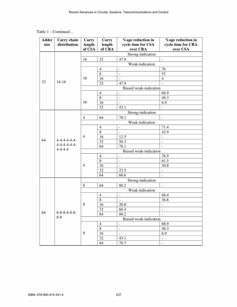
Table 1 – Continued…
Adder
size
Carry chain
distribution
Carry
length
of CSA
Carry
length
of CRA
%age reduction in
cycle time for CSA
over CRA
%age reduction in
cycle time for CRA
over CSA
32
16-16
Strong-indication
16 32 47.9 -
Weak-indication
16
4 - 76
8 - 52
16 - 4
32 47.9 -
Biased weak-indication
16
4 - 68.9
8 - 48.3
16 - 6.9
32 43.1 -
64
4-4-4-4-4-4-
4-4-4-4-4-4-
4-4-4-4
Strong-indication
4 64 78.1 -
Weak-indication
4
4 - 71.4
8 - 42.9
16 12.5 -
32 56.3 -
64 78.1 -
Biased weak-indication
4
4 - 76.9
8 - 61.5
16 - 30.8
32 23.5 -
64 60.6 -
64
8-8-8-8-8-8-
8-8
Strong-indication
8 64 80.2 -
Weak-indication
8
4 - 68.4
8 - 36.8
16 20.8 -
32 60.4 -
64 80.2 -
Biased weak-indication
8
4 - 68.9
8 - 48.3
16 - 6.9
32 43.1 -
64 70.7 -
Recent Advances in Circuits, Systems, Telecommunications and Control
ISBN: 978-960-474-341-4 237

Table 1 – Continued…
Adder
size
Carry
chain
distribution
Carry
length
of CSA
Carry
length
of CRA
%age reduction in
cycle time for CSA
over CRA
%age reduction in
cycle time for CRA
over CSA
64
16-16-16-16
Strong-indication
16 64 71.9 -
Weak-indication
16
4 - 77.8
8 - 55.6
16 - 11.1
32 43.8 -
64 71.9 -
Biased weak-indication
16
4 - 72.7
8 - 54.6
16 - 18.2
32 35.3 -
64 66.7 -
64
32-32
Strong-indication
32 64 48.9 -
Weak-indication
32
4 - 87.8
8 - 75.5
16 - 51
32 - 2
64 48.9 -
Biased weak-indication
32
4 - 83
8 - 71.7
16 - 49
32 - 3.8
64 46.5 -
128
4-4-4-4-4-4-
4-4-4-4-4-4-
4-4-4-4-4-4-
4-4-4-4-4-4-
4-4-4-4-4-4-
4-4
Strong-indication
4 128 80.7 -
Weak-indication
4
4 - 83.8
8 - 67.6
16 - 35.1
32 22.9 -
64 61.5 -
128 80.7 -
Biased weak-indication
4
4 - 87.3
8 - 78.9
16 - 61.9
32 - 28.1
64 28.3 -
128 63.8 -
Recent Advances in Circuits, Systems, Telecommunications and Control
ISBN: 978-960-474-341-4 238

Table 1 – Continued…
Adder
size
Carry
chain
distribution
Carry
length
of CSA
Carry
length
of CRA
%age reduction in
cycle time for CSA
over CRA
%age reduction in
cycle time for CRA
over CSA
128
8-8-8-8-8-8-
8-8-8-8-8-8-
8-8-8-8
Strong-indication
8 128 89.8 -
Weak-indication
8
4 - 69.2
8 - 38.5
16 18.8 -
32 59.4 -
64 79.7 -
128 89.8 -
Biased weak-indication
8
4 - 70
8 - 50
16 - 10
32 41.2 -
64 69.7 -
128 84.6 -
128
16-16-16-
16-16-16-
16-16
Strong-indication
16 128 83.9 -
Weak-indication
16
4 - 80.7
8 - 61.3
16 - 22.6
32 35.4 -
64 67.2 -
128 83.9 -
Biased weak-indication
16
4 - 78.1
8 - 63.4
16 - 34.2
32 19.6 -
64 58.6 -
128 78.9 -
128
32-32-32-32
Strong-indication
32 128 73.4 -
Weak-indication
32
4 - 88.2
8 - 76.5
16 - 52.9
32 - 5.9
64 46.9 -
128 73.4 -
Biased weak-indication
32
4 - 84.2
8 - 73.7
16 - 52.6
32 - 10.5
64 42.4 -
128 70.8 -
Recent Advances in Circuits, Systems, Telecommunications and Control
ISBN: 978-960-474-341-4 239

Table 1 – Continued…
Adder
size
Carry
chain
distribution
Carry
length
of CSA
Carry
length
of CRA
%age reduction in
cycle time for CSA
over CRA
%age reduction in
cycle time for CRA
over CSA
128
64-64
Strong-indication
64 128 49.5 -
Weak-indication
64
4 - 93.8
8 - 87.6
16 - 75.3
32 - 50.5
64 - 1
128 49.5 -
Biased weak-indication
64
4 - 91.1
8 - 85.2
16 - 73.3
32 - 49.5
64 - 1.9
128 48.2 -
256
4-4-4-4-4-4-
4-4-4-4-4-4-
4-4-4-4-4-4-
4-4-4-4-4-4-
4-4-4-4-4-4-
4-4-4-4-4-4-
4-4-4-4-4-4-
4-4-4-4-4-4-
4-4-4-4-4-4-
4-4-4-4-4-4-
4-4-4-
4
Strong-indication
4 256 64 -
Weak-indication
4
4 - 91.3
8 - 82.6
16 - 65.2
32 - 30.4
64 28.1 -
128 64.1 -
256 82 -
Biased weak-indication
4
4 - 93.3
8 - 88.9
16 - 80
32 - 62.2
64 - 26.7
128 30.8 -
256 65.1 -
Recent Advances in Circuits, Systems, Telecommunications and Control
ISBN: 978-960-474-341-4 240
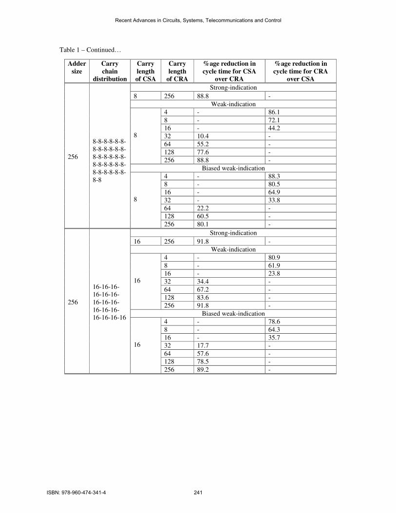
Table 1 – Continued…
Adder
size
Carry
chain
distribution
Carry
length
of CSA
Carry
length
of CRA
%age reduction in
cycle time for CSA
over CRA
%age reduction in
cycle time for CRA
over CSA
256
8-8-8-8-8-8-
8-8-8-8-8-8-
8-8-8-8-8-8-
8-8-8-8-8-8-
8-8-8-8-8-8-
8-8
Strong-indication
8 256 88.8 -
Weak-indication
8
4 - 86.1
8 - 72.1
16 - 44.2
32 10.4 -
64 55.2 -
128 77.6 -
256 88.8 -
Biased weak-indication
8
4 - 88.3
8 - 80.5
16 - 64.9
32 - 33.8
64 22.2 -
128 60.5 -
256 80.1 -
256
16-16-16-
16-16-16-
16-16-16-
16-16-16-
16-16-16-16
Strong-indication
16 256 91.8 -
Weak-indication
16
4 - 80.9
8 - 61.9
16 - 23.8
32 34.4 -
64 67.2 -
128 83.6 -
256 91.8 -
Biased weak-indication
16
4 - 78.6
8 - 64.3
16 - 35.7
32 17.7 -
64 57.6 -
128 78.5 -
256 89.2 -
Recent Advances in Circuits, Systems, Telecommunications and Control
ISBN: 978-960-474-341-4 241

Table 1 – Continued…
Adder
size
Carry
chain
distribution
Carry
length
of CSA
Carry
length
of CRA
%age reduction in
cycle time for CSA
over CRA
%age reduction in
cycle time for CRA
over CSA
256
32-32-32-
32-32-32-
32-32
Strong-indication
32 256 85.7 -
Weak-indication
32
4 - 89.1
8 - 78.2
16 - 56.4
32 - 12.7
64 42.7 -
128 71.4 -
256 85.7 -
Biased weak-indication
32
4 - 86.2
8 - 76.9
16 - 58.5
32 - 21.5
64 34.3 -
128 66.7 -
256 83.2 -
256
64-64-64-64
Strong-indication
64 256 74.2 -
Weak-indication
64
4 - 93.9
8 - 87.9
16 - 75.8
32 - 51.5
64 - 3
128 48.4 -
256 74.2 -
Biased weak-indication
64
4 - 91.4
8 - 85.7
16 - 74.3
32 - 51.4
64 - 5.7
128 46.2 -
256 72.9 -
Recent Advances in Circuits, Systems, Telecommunications and Control
ISBN: 978-960-474-341-4 242

Table 1 – Continued…
Adder
size
Carry
chain
distribution
Carry
length
of CSA
Carry
length
of CRA
%age reduction in
cycle time for CSA
over CRA
%age reduction in
cycle time for CRA
over CSA
256
128-128
Strong-indication
128 256 49.7 -
Weak-indication
128
4 - 96.9
8 - 93.8
16 - 87.6
32 - 75.1
64 - 50.3
128 - 0.5
256 49.7 -
Biased weak-indication
128
4 - 95.4
8 - 92.4
16 - 86.3
32 - 74.1
64 - 49.8
128 - 1
256 49.1 -
End of Table 1
Recent Advances in Circuits, Systems, Telecommunications and Control
ISBN: 978-960-474-341-4 243