Master’s Thesis in Electrical Engineering by Adnan Daud Khan & Muhammad...
58
Technical report, IDE0946, June 2009 PHOTONIC CRYSTAL DESIGNS (PCD) Master’s Thesis in Electrical Engineering by Adnan Daud Khan & Muhammad Noman School of Information Science, Computer and Electrical Engineering Halmstad University
Transcript of Master’s Thesis in Electrical Engineering by Adnan Daud Khan & Muhammad...

Technical report, IDE0946, June 2009
PHOTONIC CRYSTAL DESIGNS
(PCD)
Master’s Thesis in Electrical Engineering
by
Adnan Daud Khan & Muhammad Noman
School of Information Science, Computer and Electrical Engineering
Halmstad University
Title
PHOTONIC CRYSTAL DESIGNS (PCD)
Master’s thesis in Electrical Engineering
School of Information Science, Computer and Electrical Engineering
Halmstad University
Box 823, S-301 18 Halmstad, Sweden
June 2009

Description of cover page picture: Triangular Photonic Crystal Cavity.


i
Preface
The field of wireless communications develops upon electromagnetism principles.
Advancement of the AM radio, Radio navigation, Commercial AM, FM radio, Microwave
communication, Radar, Communication satellites, cellular phones, AMPS, GSM, 3G mobile
systems etc are some of the offerings of electromagnetism.
The field of electromagnetism inspire by its applications in field of high-speed
communications, modelling of microwave devices, optics, wireless communications,
Electromagnetic Interference, filtering, Cellular communications, antenna, electromagnetic band
gap structure, imaging of human body etc.
Since the first conversation on the photonic crystals, scientists and engineers have
established that photonic crystals can be used for a huge number of applications in all areas of
engineering. Photonic crystals have exposed promising results in engineering applications
particularly in communication engineering. These photonic crystals have applications for
instance, guiding light through photonic crystal slab waveguides with fewer losses, optical
switching, optical filtering, optical cavities etc.
Electromagnetism earlier relied on mathematical simplifications. Engineering problems
involve getting solutions to partial differential equations. Although only easy problems can be
resolved by using analytical methods, the majority of the practical problems are complex enough
to solve analytically. For that reason, to solve these problems, numerical techniques are the only
existing tool. There are number of numerical techniques for time evolution of electromagnetic
fields.
So, the purpose of this project is to solve problems in electromagnetism, which are not
possible to solve analytically, by making use of numerical technique such as the finite difference
time domain (FDTD) method. We have simulated a waveguide bend, which is very useful in
photonic integrated circuits. We have worked on photonic crystal cavities and made monopole,
dipole and Quadra pole. We have also simulated a double heterostructure nano cavity to achieve
high Q-factor. All these simulations have been performed as a thesis at Halmstad University for
the degree of Master of Science with a major in Electrical Engineering.
Adnan Daud Khan & Muhammad Noman
Halmstad University, June 2009

ii
Abstract
Photonic Crystal (PC) devices are the most exciting advancement in the field of photonics.
The use of computational techniques has made considerable improvements in photonic crystals
design. We present here an ultrahigh quality factor (Q) photonic crystal slab nanocavity formed
by the local width modulation of a line defect. We show that only shifting two holes away from a
line defect is enough to attain an ultrahigh Q value. We simulated this double heterostructure
nano cavity by using Finite Difference Time Domain (FDTD) technique. We observed that
photonic crystal cavities are very sensitive to the frequency, size and position of the source. So
we must choose the right values for these parameters.

iii
CONTENTS
PREFACE --------------------------------------------------------------------------------------------------------------------------- I
ABSTRACT ------------------------------------------------------------------------------------------------------------------------ II
1. INTRODUCTION TO PHOTONIC CRYSTALS -------------------------------------------------------------------- 1
2. MAXWELL’S EQUATION FOR PHOTONIC CRYSTALS ------------------------------------------------------ 4
2.1 BLOCH WAVES AND BRILLOUIN ZONES IN PHOTONIC CRYSTALS: ----------------------------------------------------- 7
3. ONE DIMENSIONAL AND TWO DIMENSIONAL PHOTONIC CRYSTALS ----------------------------- 10
3.1 PHYSICAL ORIGIN OF PHOTONIC BAND GAP: ------------------------------------------------------------------------------ 10
3.1.1 THE SIZE OF THE BAND GAP: --------------------------------------------------------------------------------------------- 11
3.2 TWO DIMENSIONAL PHOTONIC CRYSTALS: ------------------------------------------------------------------------------- 13
3.3 COMPLETE BAND GAP FOR ALL POLARIZATIONS: ----------------------------------------------------------------------- 17
3.4 POINT DEFECTS: ------------------------------------------------------------------------------------------------------------- 18
4. PHOTONIC CRYSTAL CAVITIES ----------------------------------------------------------------------------------- 19
4.1 QUALITY FACTOR (Q): ------------------------------------------------------------------------------------------------------ 20
5. FINITE DIFFERENCE TIME DOMAIN METHOD (FDTD) ---------------------------------------------------- 22
5.1 INTRODUCTION: -------------------------------------------------------------------------------------------------------------- 22
5.2 FINITE-DIFFERENCE EXPRESSION OF MAXWELL’S EQUATIONS: ------------------------------------------------------- 23
6. ELECTROMAGNETIC SIMULATIONS TOOL ------------------------------------------------------------------- 28
6.1 TRANSMISSION AND REFLECTION SPECTRUM: --------------------------------------------------------------------------- 28
6.2 RESONANT MODES: --------------------------------------------------------------------------------------------------------- 29
6.3 HARMINV: -------------------------------------------------------------------------------------------------------------------- 29
6.4 BOUNDARY CONDITIONS IN MEEP: --------------------------------------------------------------------------------------- 30
6.5 UNITS IN MEEP: ------------------------------------------------------------------------------------------------------------- 31
7. SIMULATIONS OF PHOTONIC CRYSTAL DEVICES --------------------------------------------------------- 32
7.1 PHOTONIC CRYSTAL WAVEGUIDES: -------------------------------------------------------------------------------------- 32
7.2 CAVITY SIMULATIONS: ----------------------------------------------------------------------------------------------------- 35
7.3 ULTRA-HIGH LINE MODULATED CAVITY: ------------------------------------------------------------------------------- 37
7.3.1 RESULTS: ------------------------------------------------------------------------------------------------------------------- 38
7.3.2 DISCUSSION: --------------------------------------------------------------------------------------------------------------- 41
CONCLUSION -------------------------------------------------------------------------------------------------------------------- 48
REFERENCES -------------------------------------------------------------------------------------------------------------------- 49
iv
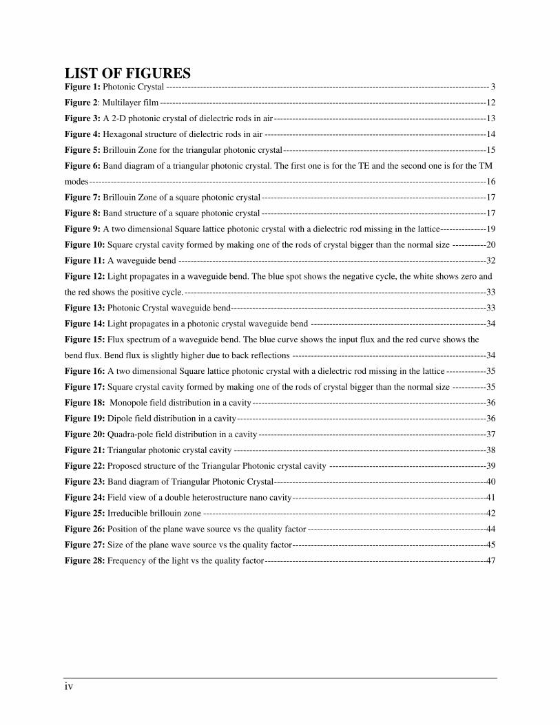
LIST OF FIGURES Figure 1: Photonic Crystal --------------------------------------------------------------------------------------------------------- 3
Figure 2: Multilayer film ---------------------------------------------------------------------------------------------------------- 12
Figure 3: A 2-D photonic crystal of dielectric rods in air --------------------------------------------------------------------- 13
Figure 4: Hexagonal structure of dielectric rods in air ------------------------------------------------------------------------ 14
Figure 5: Brillouin Zone for the triangular photonic crystal ------------------------------------------------------------------ 15
Figure 6: Band diagram of a triangular photonic crystal. The first one is for the TE and the second one is for the TM
modes --------------------------------------------------------------------------------------------------------------------------------- 16
Figure 7: Brillouin Zone of a square photonic crystal ------------------------------------------------------------------------- 17
Figure 8: Band structure of a square photonic crystal ------------------------------------------------------------------------- 17
Figure 9: A two dimensional Square lattice photonic crystal with a dielectric rod missing in the lattice --------------- 19
Figure 10: Square crystal cavity formed by making one of the rods of crystal bigger than the normal size ----------- 20
Figure 11: A waveguide bend ---------------------------------------------------------------------------------------------------- 32
Figure 12: Light propagates in a waveguide bend. The blue spot shows the negative cycle, the white shows zero and
the red shows the positive cycle. -------------------------------------------------------------------------------------------------- 33
Figure 13: Photonic Crystal waveguide bend ----------------------------------------------------------------------------------- 33
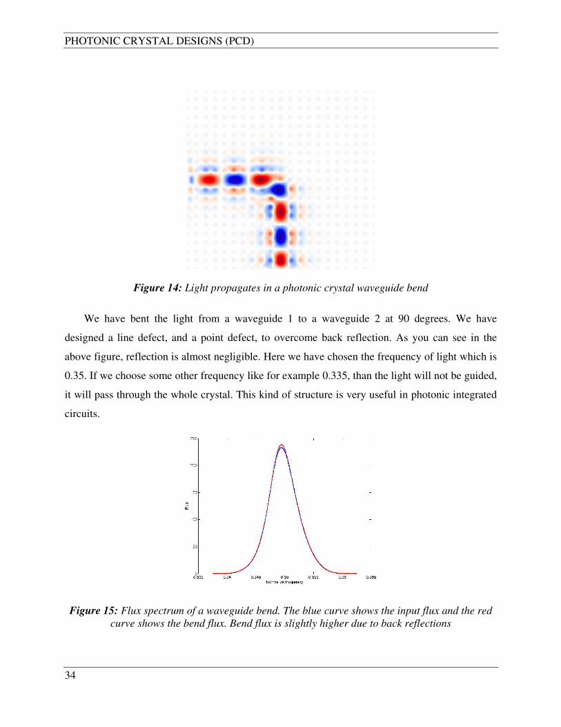
Figure 14: Light propagates in a photonic crystal waveguide bend --------------------------------------------------------- 34
Figure 15: Flux spectrum of a waveguide bend. The blue curve shows the input flux and the red curve shows the
bend flux. Bend flux is slightly higher due to back reflections --------------------------------------------------------------- 34
Figure 16: A two dimensional Square lattice photonic crystal with a dielectric rod missing in the lattice ------------- 35
Figure 17: Square crystal cavity formed by making one of the rods of crystal bigger than the normal size ----------- 35
Figure 18: Monopole field distribution in a cavity ---------------------------------------------------------------------------- 36
Figure 19: Dipole field distribution in a cavity --------------------------------------------------------------------------------- 36
Figure 20: Quadra-pole field distribution in a cavity -------------------------------------------------------------------------- 37
Figure 21: Triangular photonic crystal cavity ---------------------------------------------------------------------------------- 38
Figure 22: Proposed structure of the Triangular Photonic crystal cavity --------------------------------------------------- 39
Figure 23: Band diagram of Triangular Photonic Crystal --------------------------------------------------------------------- 40
Figure 24: Field view of a double heterostructure nano cavity --------------------------------------------------------------- 41
Figure 25: Irreducible brillouin zone -------------------------------------------------------------------------------------------- 42
Figure 26: Position of the plane wave source vs the quality factor ---------------------------------------------------------- 44
Figure 27: Size of the plane wave source vs the quality factor --------------------------------------------------------------- 45
Figure 28: Frequency of the light vs the quality factor ------------------------------------------------------------------------ 47

INTRODUCTION TO PHOTONIC CRYSTALS
1
1. INTRODUCTION TO PHOTONIC CRYSTALS
A crystal represents a periodic array of atoms or molecules. The arrangement with which
the atoms or molecules are repeated in space is called the crystal lattice. Photonic crystals are
artificial crystal structures that manipulate the propagation of light. Photonic crystals are also
called periodic materials of light or photonic band gap materials. These crystal structures
manipulate light in the same way that electronic and semi conducting materials manipulate the
electron waves due to periodic potential. We can also name them “Semiconductors of Light”
[17].
In electronic band gap materials, the electronic band gap is an array of discrete energies
that electron waves cannot occupy. All the fancy functionalities carried out by the improvements
in the field of electronic materials and devices made up of these materials are due to the control
of the availability of the electrons and holes above and below the electronic band gap. The
existence of the electronic band gap depends on the material, its crystal structure, the type of
atoms or group of atoms in the material. By varying the sorts of materials, and therefore using
different atoms called dopant atoms. One can dramatically vary the properties of the materials. In
electronic and semi conducting materials, atoms nearby to each other are separated by a quarter
of a nanometer. Photonic band gap materials, or photonic crystals, have comparable sorts of
structure, but at a larger scale than electronic materials. In photonic crystals, the spacing can be of
the order of 400 nanometers. The spacing works as analogous to atoms in semiconductors. In
general, however, the wavelengths of the wave to be controlled should be close to the spacing in
the photonic crystal. We can take an example of a material having a specific number of holes,
which are spaced a few hundred nanometers from each other. The light entering the material will
partially refract and reflect, creating complex patterns of light beams. These light beams will
strengthen, or cancel, at certain locations according to the light’s wavelength, the direction of the
light propagation, the dielectric constant of the material, and the arrangement of the crystal. If the
light is cancelled completely within a specific range of wavelengths, leading to a band gap for the
light, i.e. the light having that range of wavelengths, it will not propagate through the crystal.
Also if the properties of the photonic crystal are changed the same way, changing the doping

PHOTONIC CRYSTAL DESIGNS (PCD)
2
atoms in semiconductors, it will change the performance of the crystal for the light beam
propagating through it.
Metallic waveguides and cavities can be related to photonic crystals. They are
extensively used to manage the transmission of microwaves. The transmission of the
electromagnetic waves will be disallowed by the walls of the metallic cavity with frequencies
lower than a particular threshold frequency, and a metallic waveguide accept transmission just at
its axis. It would be good to have these similar potentials for electromagnetic waves with
frequencies beyond the microwave scheme, like the visible light. However visible light energy is
rapidly dissipated within metallic machinery, which renders this technique of optical control
impractical to generalize a wider choice of frequencies. We can build a millimetre dimension
photonic crystal of a known geometry for the control of microwave, or else for micrometer
dimension for handling the infrared.
Photonic crystals are considered to be an engagement of electromagnetism and solid-
state physics. Crystal arrangements are populace of solid state physics, except that the electrons
are replaced by electromagnetic waves in photonic crystals [1].
The periodic layers in the photonic crystal reflect light beams with a range of
wavelengths, producing a photonic band gap. Hence, we have a certain range of frequencies of
light which cannot propagate through the photonic crystal. Outside the band gap region, the shape
and speed of light beam can be very different and can be manipulated This permits us to control
the flow of light and guide it efficiently through the guiding structure, slowing it down to a
desired speed. Photonic crystals have so far been used to make efficient optical switches, optical
cavities, optical filters, and optical waveguides, and can be used to make optical circuits in future
[4][8][14].
The figure below shows the photonic crystals, which contains the high dielectric and low
dielectric regions.

INTRODUCTION TO PHOTONIC CRYSTALS
3
Figure 1: Photonic Crystal
High dielectric
Low dielectric

PHOTONIC CRYSTAL DESIGNS (PCD)
4
2. MAXWELL’S EQUATION FOR PHOTONIC
CRYSTALS
The investigation and study of wave propagation in periodic media was first made by
Felix Bloch [1][2]. He showed that the wave propagation in periodic media can be successfully
accomplished without scattering of the waves. He proved that the wave drifting in the periodic
medium is modulated by a periodic function. This periodic function is due to the periodicity of
the structure of the medium, identical to the travelling of the electronic waves in the crystal
structures. The identical analogue can be applied to the electromagnetic wave propagation but,
here, the periodicity is in the dielectric difference of the medium. We start the mathematical
analysis by Maxwell’s curl equations.
0=∂
∂+×∇
t
BE
Jt
DH =
∂
∂−×∇
( 2.1)
ρ=⋅∇
=⋅∇
D
B 0
The quantities E and H are the electric and magnetic fields, measured in units of [volts/m]
and [Ampere/m] respectively. The quantities D and B are the electric and magnetic flux densities
respectively. In linear, isotropic and non-dispersive materials, the E and H fields, relate to electric
and magnetic flux through the following equations:
EED ro ξξξ == (2.2)
HHB ro µµµ ==

MAXWELL’S EQUATION FOR PHOTONIC CRYSTALS
5
Now assume no current flow or charge density in the system, then:
0=∂
∂+×∇
t
BE (2.3)
0=∂
∂−×∇
t
DH
So
0.
0.
=∇
=∇
∂
∂=×∇
∂
∂−=×∇
E
H
t
EH
t
HE
ro
o
εε
µ
(2.4)
Generally, E and H are both complex functions of space and time, since the Maxwell
equations are linear, though, from the spatial dependence, we can break up the time dependence
by increasing the fields into a set of harmonic-modes. So the harmonic-mode as a spatial
prototype or “mode profile” times a complex exponential is set by:
ti
ti
erEtrE
erHtrH
ω
ω
−
−
=
=
)(),(
)(),( (2.5)
By putting equation (2.5) in equation (2.4), the two divergence equations are given by:
0)(.
0)(.
=∇
=∇
rE
rH (2.6)
The two curl equations relate E(r) to H(r) is:
)()(
)()(
rEirH
rHirE
ro
o
εωε
ωµ
=×∇
−=×∇ (2.7)
PHOTONIC CRYSTAL DESIGNS (PCD)
6
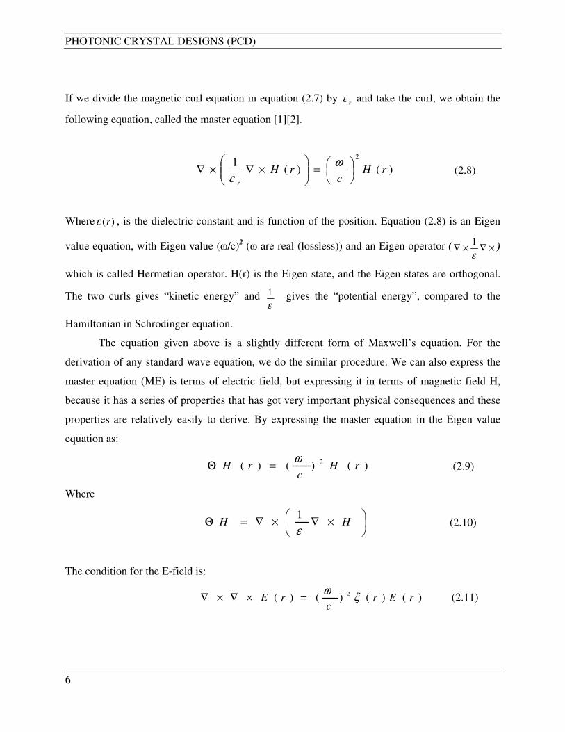
If we divide the magnetic curl equation in equation (2.7) by rε and take the curl, we obtain the
following equation, called the master equation [1][2].
)()(1
2
rHc
rHr
=
×∇×∇
ω
ε (2.8)
Where )(rε , is the dielectric constant and is function of the position. Equation (2.8) is an Eigen
value equation, with Eigen value (ω/c)2 (ω are real (lossless)) and an Eigen operator ( ×∇×∇
ε
1 )
which is called Hermetian operator. H(r) is the Eigen state, and the Eigen states are orthogonal.
The two curls gives “kinetic energy” and ε
1 gives the “potential energy”, compared to the
Hamiltonian in Schrodinger equation.
The equation given above is a slightly different form of Maxwell’s equation. For the
derivation of any standard wave equation, we do the similar procedure. We can also express the
master equation (ME) is terms of electric field, but expressing it in terms of magnetic field H,
because it has a series of properties that has got very important physical consequences and these
properties are relatively easily to derive. By expressing the master equation in the Eigen value
equation as:
)()()( 2
rHc
rHω
=Θ (2.9)
Where
×∇×∇=Θ HH
ε
1 (2.10)
The condition for the E-field is:
)()()()( 2 rErc
rE ξω
=×∇×∇ (2.11)

MAXWELL’S EQUATION FOR PHOTONIC CRYSTALS
7
It is referred to as a generalized Eigen problem, since there are operators on both sides of this
equation. It is an easy matter to change this into a normal, Eigen problem by dividing equation
(2.11) byξ , but then operator is not a Hermitian.
We can reinstate a simpler transversality constraint by using D in place of E, since 0. =∇ D .
Putting oE
Dξ for E in equation (2.11) and, to keep the operator Hermitian, divide both sides by
ξ , which yields:
)()(
1)()(
)(
1
)(
1 2rD
rcrD
rr ξ
ω
ξξ=×∇×∇ (2.12)
This equation looks like being much more complex, so we prefer the “H” for numerical
calculations.
2.1 Bloch Waves and Brillouin Zones in Photonic Crystals:
Similar to traditional crystals of atoms or molecules, photonic crystals do not have
continuous translational symmetry. They have (photonic crystal) discrete translational symmetry
i.e. under translations of any distance they are not invariant but, instead, just distances, which are
the multiples of certain fixed step lengths [1][2].
In photonic crystals, the wave propagates according to the Bloch’s theorem [1][2]. The
propagation is a function of a periodicity in the medium. In optical periodic media (photonic
crystals), there is a periodic variation in dielectric constants. The refractive indices are functions
of positions.
)()(
)()(
axx
axx
+=
+=
µµ
εε (2.13)
Where, ‘a’ is any arbitrary lattice vector. The above equations state that the medium repeats its
properties after position ‘x+a’.
The Bloch’s theorem is given by

PHOTONIC CRYSTAL DESIGNS (PCD)
8
( ) )(),( xHetxHk
txki rrrrr
rrω−⋅= (2.14)
Where ( )txkie
ω−⋅rr
is a plane wave, and )( xHk
rrr is periodic “envelop”. K is conserved, i.e.
no scattering of Bloch wave occurs. ω are discrete )(knω .
It is important to know that Bloch state having wave vector ‘k’, and the Bloch state having wave
vector ‘k+mc’, are the same. So the k’s that are different by integral multiples of c = 2π/a, are
not distinct from the physical point of view. Therefore, the frequencies of mode should also be
periodic in k. K exists in the range -π/a < k < π/a. This area of imperative, non-redundant values
of k is known as the Brillouin zone. The shortest area inside the Brillouin zone, for which the
)(knω (frequency bands) are not linked by symmetry, is known as irreducible Brillouin zone.
The irreducible Brillouin zone consists of a triangular block with 1/8 the area of the complete
Brillouin zone, and the remainder of the zone contains redundant versions of the irreducible zone.
When the dielectric is periodic in three dimensions, then dielectric is invariant in that
case under translations through a large number of three dimensional lattice vectors R. These
vectors can be inscribed as a specific arrangement of the three primitive lattice vectors, (a1, a2,
a3), that are called to “span” the space of lattice vectors, or each namalaR 321++= for
various integers l, m, and n, the vectors (a1, a2, a3) provide three primitive reciprocal lattice
vectors (c1, c2, c3)
So that
jiji ca ,2. πδ= (2.15)
These reciprocal vectors span a reciprocal lattice of their individual that is occupied by the wave
vectors. The modes of a 3D periodic system are Bloch states that can be marked by a Bloch wave
vector
332211 ckckckK ++= (2.16)
Where, “K” is in the Brillouin zone. Every value of the wave vector K within the Brillouin zone
recognizing an Eigen state of ×∇×∇ε
1 with frequency )(kω and an eigenvector kH of the type
MAXWELL’S EQUATION FOR PHOTONIC CRYSTALS
9
)()( .
ruerH k
rik
k = (2.17)
Where )(ruk , a periodic function of the lattice is: )()( Rruru kk += for each lattice vectors R.

PHOTONIC CRYSTAL DESIGNS (PCD)
10
3. ONE DIMENSIONAL AND TWO DIMENSIONAL
PHOTONIC CRYSTALS
3.1 Physical origin of Photonic band gap:
The electronic band gap in crystal structure occurs because of the relations of electronic
waves with the periodic potential due to ion cores, and this gap is the states of energies that
electrons cannot take up. In the same way, in electrodynamics, the photonic band gap is an array
of frequencies for the light wave, where there are no propagating explanations to Maxwell’s
equation. There may be band gaps which are incomplete, but can survive for several set of wave
vectors, polarization and/or symmetries. The basis of both the band gaps is alike. We will look at
the band gap of a photonic crystal with the support of the analysis of one dimensional photonic
crystal.
Assume the situation of one dimensional photonic crystal, with the periodicity in the
crystal is “a”. The one dimensional photonic crystal contains alternating layers of dielectric
constants. The result of this assembly to the incident waves is comparable to the concept of
interference in thin films. When a wave inserts into the crystal, partial reflections and
transmissions occur from every boundary. The waves which are reflected and transmitted either
interfere constructively or destructively. For a specific series of frequencies, the wave moving in
the forward direction and the waves reflecting off the interfaces, interfere destructively, with the
intention that there are no travelling waves in the forward direction for that series (range) of
frequencies. This range of frequencies is known as photonic band gap, where the wave is trapped.
For the one dimensional photonic crystal, the wave vectors k = -π/a and π/a results in standing
waves with wavelengths 2a. Because of the symmetry of the crystal structure, we can place its
nodes either in low refractive index layer (or low dielectric region) or high refractive index layer
(or high dielectric region). Low frequency wave vectors will focus their energy in the high index
region, and high frequency wave vectors will focus their energy in the low index region. This
focusing of energies of high and low frequencies creates a band gap of frequencies.
The band over and under the gap can be notable where the energy of their modes is
focusing i.e. inside the high or low dielectric area. Normally, in the two and three dimensional

ONE DIMENSIONAL AND TWO DIMENSIONAL PHOTONIC CRYSTALS
11
crystals, the low dielectric regions are air regions. Therefore, it is reasonable to describe the band
over a photonic band gap as the air band and the band under a gap as the dielectric band. The
condition is analogous to the electronic band structure of the semiconductors, where the
conduction band and the valence band set the elementary gap.
3.1.1 The size of the band gap:
The degree of a photonic band gap can be considered by its frequency width ω∆ .
However, this is not a very fine calculation. When the crystal was expanded by some factor e,
then the equivalent band gap would have a width e
ω∆ . Here, we will introduce a gap-midgap
ratio, which is very useful, and is independent of the scale of the crystal [1]. Suppose mω is the
frequency at the middle of the gap, so the gap-midgap ratio is given by
mωω∆
Where ω∆ is the frequency width of the photonic band gap. It is normally expressed as a
percentage. So if the system is scaled up or down, every frequency scale consequently, other than
the gap-midgap ratio because it is independent of the scale of the crystal. Therefore, whenever we
refer to the size or dimensions of a gap, we mean the gap-midgap ratio. The frequency and the
wave vector are always plotted in dimensionless units, and is given by:
ca
πω
2 and
π2ka
The dimensionless frequency is equal to λ
a , where λ is the vacuum wavelength that is given
byω
πλ c2= .
Now consider an example of a multilayer film, as shown in figure 2, with feeble
periodicity. Here, we can obtain an easy formula for the size of the band gap. If we suppose that,
the two materials have dielectric constants “ε ” and “ εε ∆+ ”, and thickness “a-d” and “d” in a
multilayer film. Here, we will see that if the dielectric difference is fragile i.e., 1<<∆ε
ε or the
thickness “d/a” is minute. After that the gap-midgap ratio among the first two bands is given by:
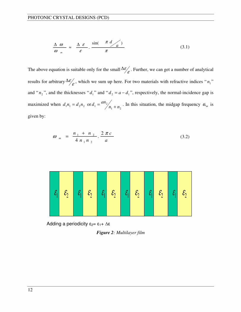
PHOTONIC CRYSTAL DESIGNS (PCD)
12
π
π
ε
ε
ω
ω )sin(. a
d
m
∆≈
∆ (3.1)
The above equation is suitable only for the smallε
ε∆ . Further, we can get a number of analytical
results for arbitraryε
ε∆ , which we sum up here. For two materials with refractive indices “ 1n ”
and “ 2n ”, and the thicknesses “ 1d ” and “ 12 dad −= ”, respectively, the normal-incidence gap is
maximized when 2211 ndnd = or21
21 nn
and
+= . In this situation, the midgap frequency mω is
given by:
a
c
nn
nnm
πω
2.
4 21
21 += (3.2)
Figure 2: Multilayer film
ε1
ε2
ε1
ε2
ε1
ε2
ε1
ε2
ε1
ε2
ε1
ε2
Adding a periodicity ε2= ε1+ ∆ε

ONE DIMENSIONAL AND TWO DIMENSIONAL PHOTONIC CRYSTALS
13
3.2 Two dimensional photonic crystals:
Two-dimensional photonic crystals have variation in the dielectric constant, or refractive
index, of the material in space in two dimensions, while it is homogenous along the third
dimension. Typical example of a two dimensional photonic crystal is a square lattice of dielectric
rods in air as shown in the figure.
Figure 3: A 2-D photonic crystal of dielectric rods in air
For some values of the spacing between the columns of the dielectric rods, the crystal can
have a photonic band gap in the xy-plane. The incident light in this plane does not propagate
through the crystal at any angle, contrary to multilayer thin film (1-D photonic crystal) which
reflected light at normal incident of light.
Symmetries of the crystal play a very significant role in description of the electromagnetic
modes in the crystal. Two-dimensional crystal has discrete translational symmetry in xy-plane.
This means that the dielectric constant is periodic only if it follows the position of the lattice point
is linear combination of the primitive lattice vectors. The main fact about the photonic crystals in
two dimensions is to understand the fields in 2-D to be sub-divided into two polarizations. The
one is the Transverse magnetic (TM) mode and the other is the Transverse electric (TE) mode. In
the earlier case, the magnetic field is in the xy-plane and the electric field is perpendicular, i.e. in

PHOTONIC CRYSTAL DESIGNS (PCD)
14
the z-direction, and in the latter case, the electric field is in the crystal plane and the magnetic
field is perpendicular. Corresponding to the polarizations, there are two fundamental topologies
for two-dimensional photonic crystals, as shown in figure 4. High index rods are enclosed by low
index and low-index holes in high index, in other words, dielectric rods in air or air holes in a
dielectric substrate.
There are two ways to line up the dielectric rods in air or air holes in dielectric substrate.
One category of arrangement is called square lattice arrangement while the other one is called the
triangular, or hexagonal, arrangement. Figure 3 shows the square lattice arrangements. Likewise,
the following figure shows the hexagonal or triangular arrangements of two-dimensional photonic
crystals.
Figure 4: Hexagonal structure of dielectric rods in air
Square lattice arrangement of the dielectric rods in air or air holes in dielectric substrate
guides us to different sorts of band gaps of TM and TE polarizations. In a square lattice, TM
polarized mode band gaps are favored, for the reason that isolated high index regions compel TM
modes to have dissimilar fill factors, due to the appearance of the node in the higher mode that, in
turn, leads to higher TM gaps and lower TE gaps. The TE modes in square lattice were forced to
go through the low index regions for the field line to be continuous, so the fill factors for the
consecutive modes are low and not very far away. The point to understand is that TM band gaps
are favored in a lattice of high index region while TE modes are supported in a linked region.

ONE DIMENSIONAL AND TWO DIMENSIONAL PHOTONIC CRYSTALS
15
To achieve better and larger band gaps, it is necessary to arrange photonic crystals with
both isolated and connected regions of high index region. This is accomplished by the triangular
or hexagonal arrangement of air holes or dielectric rods. The triangular or hexagonal lattice gives
better band gaps for both the polarizations. The band gaps for both the arrangements of two-
dimensional photonic crystals are given below. Figure 6 shows the band structure of the
triangular photonic crystal and figure 8 shows the band structure of the square photonic crystal.
We draw the band structure for the triangular photonic crystal by using brillouin zone as shown in
the figure below.
Kr
Figure 5: Brillouin Zone for the triangular photonic crystal
We get this brillouin zone by drawing perpendiculars from each lattice point in figure 4. This
brillouin zone is large enough, we do not need to go inside of it, we will just travel at its edges.
So for that we will draw a triangle inside of it. This triangle is called the irreducible brillouin
zone. If we rotate this triangle, than we can construct the whole brillouin zone. When we move
from Γ to K, K to M and from M to Γ than the first band will be formed, than the second band
and so on as shown in figure 6.

PHOTONIC CRYSTAL DESIGNS (PCD)
16
Figure 6: Band diagram of a triangular photonic crystal. The first one is for the TE and the
second one is for the TM modes
ω
ω

ONE DIMENSIONAL AND TWO DIMENSIONAL PHOTONIC CRYSTALS
17
For the square photonic crystal we get the following brillouin zone by drawing perpendiculars
from each lattice point in figure 3.
Figure 7: Brillouin Zone of a square photonic crystal
So here we draw the band structure by moving from Γ to X, X to M and from M to Γ.
Figure 8: Band structure of a square photonic crystal
3.3 Complete Band Gap for All Polarizations:
A photonic crystal can be designed that has a band gaps for both TM and TE polarizations.
By manipulating the lattice dimensions, we can even have the complete band gap for all
polarizations.
ω

PHOTONIC CRYSTAL DESIGNS (PCD)
18
Due to the appearance of a node in the higher frequency mode, the isolated high dielectric
constant spots of the square lattice of dielectric columns forced successive TM modes in order to
have different concentration factors. This results in the large TM photonic band gap.
In the square lattice of dielectric rods, the field lines had to cross dielectric boundaries so
the TE modes were forced to go through the low dielectric constant regions. As a consequence of
this, for successive modes, the concentration factors were both near and low.
In short, we can say that, TM band gaps are privileged in a lattice of isolated high dielectric
constant regions, and also the TE band gaps are privileged in a connected lattice.
It looks impractical to arrange a photonic crystal together with connected regions of
dielectric material and isolated spots. The solution is a sort of compromise; we can put a
triangular lattice of low dielectric constant columns inside a medium with high dielectric
constant. If the radius of the column is very large, then the spots between the columns seem to be
localized regions of high dielectric constant material, which are connected to the adjacent spots.
3.4 Point Defects:
In 2-D, we can replace a column with another column whose shape, size, or dielectric
constant is different, or remove a single column from the crystal. Perturbing a single lattice spot
causes a defect, and this perturbation is localized to a specific point in the plane; we called this
perturbation as a point defect.
PHOTONIC CRYSTAL CAVITIES
19
4. PHOTONIC CRYSTAL CAVITIES
One of the important applications of photonic crystals is cavities. They behave like optical
micro-cavities for light confinement to small dimensions and volumes comparable to the
wavelength of the light. These devices work on the basis of resonant circulation, which means
that light can be trap inside the cavity when resonant mode is formed. Photonic crystal cavities
can be used in a variety of applications, such as micro cavities, which coax quantum dots to emit
spontaneous emissions in the required direction; they can also be used to control the laser
emission for long distance optical communication through optical fiber etc [14][18].
An ideal cavity has a very sharp resonant frequency and confines the light for an indefinite
period. When cavity deviates from its ideal behavior, it leads to a characteristic parameter, known
as Q-factor. The Q-factor depends directly on the time of the light confinement in the cavity, in
terms of optical period.
Photonic crystals are the analog of the semiconductors in electronic devices. Single or
multiple defects in the photonic crystal give rise to the micro-cavities. These cavities are better
than the conventional cavities because they are spectrally more efficient and pure. The
conventional cavities, which are made by etching or by the oxide confinement, usually cause non-
radiative defects. A better way is to employ a cavity by periodic variation in the dielectric
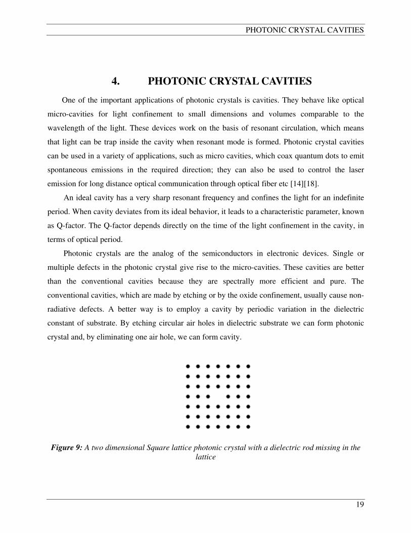
constant of substrate. By etching circular air holes in dielectric substrate we can form photonic
crystal and, by eliminating one air hole, we can form cavity.
Figure 9: A two dimensional Square lattice photonic crystal with a dielectric rod missing in the
lattice

PHOTONIC CRYSTAL DESIGNS (PCD)
20
Figure 10: Square crystal cavity formed by making one of the rods of crystal bigger than the
normal size
The frequencies in the crystal’s band gap will not propagate through it, but light will be
trapped by the defect, having the frequency equal to the resonant mode frequency formed due to
the existence of the defect. The micro-cavity that is formed has a feedback of the dominant modes
in all directions.
4.1 Quality Factor (Q):
The quality factor ‘Q’ is a measure of the losses in the cavity. Since the reflectivity of the
crystal enclosing the defect rises with the number of rods, we expect that Q will also increase
with the size of the crystal. To calculate Q, we decide to use a method which first includes
pumping energy into the cavity, then observing its decay [18]. We evoke that the quality factor is
defined as
Where E is the stored energy, ω0 is the resonant frequency, and P = -dE/dt is the dissipated
power. A resonator can consequently maintain Q oscillations before its energy decays by a factor
of π2−e (or about 0.2%) of its original value. After stimulating the resonant mode, the total energy
can be observed as a function of time, and Q can be calculated from the number or optical cycles
required for the energy to decay.
dtdE
E
P
EQ
oo
/
ωω−==

PHOTONIC CRYSTAL CAVITIES
21
The Q factor could also have been calculated using another technique. We recall that Q can
be defined as ωω
∆o , where ω∆ is the full width at half-power of the resonator’s Lorentzian
response. By calculating ω∆ from transmission calculation, we could have anticipated the value
of Q. This technique, however, would have led to larger uncertainties, especially for large values
of Q [18].
In order to compute Q, we will excite the resonance efficiently. The initial conditions are
chosen such that the pump mode and the resonant mode have a large overlap. Suppose that the
resonant mode is a monopole, we chose to initialize the system with a Gaussian field profile
centered around the defect. The energy inside the cavity was then calculated over time. Through
the early stages of the decay, every mode except the high-Q one rapidly emitted away, leaving
only the energy related with the resonant mode inside the cavity. The mode continued its gradual
exponential decay. From the rate of decay, we calculated Q.
It has been observed that Q increases exponentially with the number of rods. It reaches a
value near to 4
10 with as little as four lattices on either side of the defect [18]. Since the only
energy loss in the structure take place by tunneling through the edges of the crystal, Q does not
saturate yet for a very huge number of rods.

PHOTONIC CRYSTAL DESIGNS (PCD)
22
5. FINITE DIFFERENCE TIME DOMAIN METHOD
(FDTD)
5.1 Introduction:
The finite difference time- domain (FDTD) is a numerical method, which solves the
Maxwell’s equations. [5]. It solves electromagnetic wave propagation problems for a wide range
of applications. The FDTD technique is an increasingly admired method among scientists and
engineers in the area of computational electromagnetic.
The FDTD method can solve complex problems, but it requires large amounts of memory
and computational power. This is the reason why FDTD previously could not get the attention of
scientists and engineers because of lack of computational resources. Gradually, with the increase
in computational power, this method became popular within the computational electromagnetic
community.
Simplicity, and ease of implementation, was the main advantages of FDTD over other
computational methods, like Method of Moments (MoM) and Finite Element Method (FEM) [6].
The growing number of enhancements to, and expansions of, the method are being developed,
which is making FDTD the most preferred amongst other numerical methods.
The FDTD method is a simple and elegant way to discretize Maxwell’s equations. An
explicit finite difference approximation, both in spatial and temporal derivatives, appears in
Maxwell's equations. The method is based on central difference approximations on a staggered
Cartesian grid in space and time and, therefore, it is second order accurate in space and time
[5][6]. It calculates the E and H field everywhere in computational space, as they evolve with
time.
The finite difference time domain equations are solved for the future unknown fields, in
terms of known past fields. The two couple equations solve iteratively to advance the field in
time. This type of modelling is to test and measure fields inside a device.
FINITE DIFFERENCE TIME DOMAIN METHOD (FDTD)
23
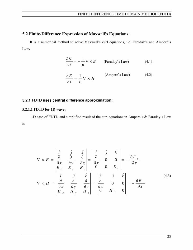
5.2 Finite-Difference Expression of Maxwell’s Equations:
It is a numerical method to solve Maxwell’s curl equations, i.e. Faraday’s and Ampere’s
Law.
(Faraday’s Law) (4.1)
(Ampere’s Law) (4.2)
5.2.1 FDTD uses central difference approximation:
5.2.1.1 FDTD for 1D wave:
1-D case of FDTD and simplified result of the curl equations in Ampere’s & Faraday’s Law
is
(4.3)
Et
H×∇−=
∂
∂
µ
1
Ht
E×∇=
∂
∂
ε
1
x
E
Hx
kji
HHH
zyx
kji
H
x
E
Ex
kji
EEE
zyx
kji
E
z
yzyx
z
zzyx
∂
∂−=
∂
∂=
∂
∂
∂
∂
∂
∂=×∇
∂
∂−=
∂
∂=
∂
∂
∂
∂
∂
∂=×∇
00
00
ˆˆˆˆˆˆ
00
00
ˆˆˆˆˆˆ

PHOTONIC CRYSTAL DESIGNS (PCD)
24
(4.4)
Now consider an Electric field:
(4.5)
Here, in the above equation, the superscript ‘q’ denotes the temporal step and ‘m’ denotes the
spatial step in the discrete 1-D grid. and are the spatial and temporal unit step sizes
respectively.
Now discretize Faraday’s law using central difference around the space-time point
(4.6)
(4.7)
Update equation for Ez field,
(4.8)
Similarly, update equation for Hy field
x
H
t
E
x
E
t
H
yz
zy
∂
∂=
∂
∂⇒
∂
∂=
∂
∂⇒
ε
µ
1
1
( ) ( ) ][,, mq
EtqxmEtxEzzz
=∆∆=
x∆ t∆
))2
1(, tqxm ∆+∆
))2
1(,))
2
1(, tqxmtqxm x
yH
t
zE
∆+∆∆+∆ ∂
∂
∂
∂=ε
x
m
q
yHm
q
yH
t
mqzEm
qzE
∆
−
+
−+
+
=∆
−+ ]
2
1[2
1
]2
1[2
1
][][1
ε
−−+
∆
∆+=
+++ ]
2
1[]
2
1[][][ 2
1
2
1
1mHmH
x
tmEmE
q
y
q
y
q
z
q
zε

FINITE DIFFERENCE TIME DOMAIN METHOD (FDTD)
25
(4.9)
5.2.1.2 FDTD for 3D wave:
Consider function n
kjiu ,, of space and time, evaluated at discrete point in grid and discrete
points in time, where n is the temporal step and i, j, k are the spatial steps in x, y, z coordinates
respectively:
Consider first partial derivative of u in x- direction, at point of time tntn ∆= .
x
uu
x
un
kji
n
kji
∆
−=
∂
∂ −+ ,,2/1,,2/1 (4.10)
Notice the half-spatial increment/ decrement in the i subscript, denoting the spatial finite
difference of x∆±2
1 . This would interleave the two adjacent E and H field components, so we
use that two consecutive spatial E field components to calculate H field component in between
them.
Similarly, we write central difference for y
u∂
∂ and z
u∂
∂ as follows:
y
uu
y
un
kji
n
kji
∆
−=
∂
∂ −+ ,2/1,,2/1, (4.11)
z
uu
z
un
kji
n
kji
∆
−=
∂
∂ −+ 2/1,,2/1,, (4.12)
Similarly, writing the central difference approximation for the function u as:
t
uu
t
un
kji
n
kji
∆
−=
∂
∂−+ 2/1
,,
2/1
,, (4.13)
Notice the half-spatial increment/ decrement in the n subscript, denoting the temporal
finite difference over t∆±2
1 . This would interleave the calculation of two adjacent E and H field
components in time intervals of t∆±2
1 .
Applying this finite difference approximation to vector components of curl operations of
Maxwell’s equation, we obtain [5]:
( )][]1[]2
1[]
2
1[ 2
1
2
1
mEmEx
tmHmH
q
z
q
z
q
y
q
y −+∆
∆++=+
−+
µ

PHOTONIC CRYSTAL DESIGNS (PCD)
26
∆
−−
∆
−
∆
+
+++
+++
++
−
++
+
++=
z
HyHy
y
HzHz
tn
kji
n
kji
n
kji
n
kji
kji
n
kji
n
kjiExEx
,2/1,1,2/1,
2/1,,2/1,1,
2/1,2/1,
2/1
2/1,2/1,
2/1
2/1,2/1,
ξ (4.14)
∆
−−
∆
−
∆
+
++−++
+−++−
++−
−
++−
+
++−=
x
HzHzz
HxHx
tn
kji
n
kji
n
kji
n
kji
kji
n
kji
n
kjiEyEy
2/1,1,12/1,1,
,1,2/11,1,2/1
2/1,1,2/1
2/1
2/1,1,2/1
2/1
2/1,2/1,2/1
ξ (4.15)
∆
−−
∆
−
∆
+
+−++−
++−++
++−
−
++−
+
++−=
y
HxHx
x
HyHy
tn
kji
n
kji
n
kji
n
kji
kji
n
kji
n
kjiEzEz
1,,2/11,1,2/1
1,2/1,11,2/1,
1,2/1,2/1
2/1
1,1,2/1
2/1
1,2/1,2/1
ξ (4.16)
∆
−−
∆
−
∆
+
+
++−
+
++−
+
++−
+
++−
++−
++−
+
++−=
y
EzEz
z
EyEy
tn
kji
n
kji
n
kji
n
kji
kji
n
kji
n
kjiHxHx
2/1
1,2/1,2/1
2/1
1,2/3,2/1
2/1
2/1,1,2/1
2/1
2/3,1,2/1
1,1,2/1
1,1,2/1
1
1,1,2/1
µ (4.17)

FINITE DIFFERENCE TIME DOMAIN METHOD (FDTD)
27
∆
−−
∆
−
∆
+
+
++
+
++
+
++−
+
+++
++
++
+
++=
z
ExEx
x
EzEz
tn
kji
n
kji
n
kji
n
kji
kji
n
kji
n
kjiHyHy
2/1
2/1,2/1,
2/1
2/3,2/1,
2/1
1,2/1,2/1
2/1
1,2/1,2/1
1,2/1,
1,2/1,
1
1,2/1,
µ (4.18)
∆
−
∆
−
∆
+
+
++−
+
+++
+
++
+
++
++
++
+
++=
x
EyEy
y
ExEx
tn
kji
n
kji
n
kji
n
kji
kji
n
kji
n
kjiHzHz
2/1
2/1,1,2/1
2/1
2/1,1,2/1
2/1
2/1,2/1,
2/1
2/1,2/3,
2/1,1,
2/1,1,
1
2/1,1,
µ (4.19)

PHOTONIC CRYSTAL DESIGNS (PCD)
28
6. ELECTROMAGNETIC SIMULATIONS TOOL
For the computational solution of arrangements using FDTD, MEEP (MIT
Electromagnetic Equation propagation) is used [3][16]. MEEP is a finite difference time domain
(FDTD) simulation open source software package, to model electromagnetic systems [16]. It is
developed at MIT. It has many features like:
1. Solving for finite difference time- domain solution, which gives a field pattern of the
system at every time step, stimulated by a source
2. FDTD simulation in 1D, 2D, 3D and cylindrical coordinates.
3. Provides distributed memory parallelism support using MPI standard.
4. Provides perfectly matched layer absorbing boundary conditions, Perfectly Electric
Conductor (PEC) and Bloch-periodic boundary conditions.
5. Exploitation of symmetries, to reduce the computational size.
6. Provides arbitrary material and source conditions.
6.1 Transmission and Reflection Spectrum:
Different finite structures are simulated, and transmission and reflection spectra are
drawn. At each frequency ω, we can separately calculate the fields and, ultimately, the
transmitted flux. However, it can calculate a response of broad-spectrum through a single
calculation much more efficiently by taking the Fourier transform of the response. This will give
the solutions for the system at different frequencies. It is much trickier if somebody wants to
calculate the transmission as well as reflection spectrum. In this case, we cannot calculate the flux
simply in the backward direction, since it would give the sum of the incident and reflected power.
Similarly, we cannot get the transmitted power simply by subtracting the incident power from
backward flux, since there will be interference between reflected and incident waves.
The solution to this is to simulate the system twice firstly without scattered and secondly
with the scattered. After that, subtract the Fourier transforms, before calculating the flux and after

ELECTROMAGNETIC SIMULATIONS TOOL
29
calculating the reflected power in the reflected plane, we will normalize to get the reflection
spectrum by the incident power.
6.2 Resonant Modes:
One of the most important features of MEEP is to calculate the resonant modes of a
structure. Consider a photonic crystal or a waveguide. MEEP can solve its harmonic (definite-ω)
modes at a given wave vector k. Similarly, consider a resonant cavity, which captures the light for
a long time in a small region, and we want to calculate the quality, factor Q and the resonant
frequency, ω.
In order to get the lifetime and frequencies with FDTD, the structure has been setup,
depending on whether it is a periodic or not, with Bloch periodic or/and absorbing boundaries.
Then the modes with a current has been excited which is placed in the system, with a short pulse.
After turning the current sources off, we get some fields in the system, which has been analyzed
to get the decay rates and frequencies.
The easiest way of harmonic analysis is to calculate the Fourier transform of the fields,
and the sharp peaks in the spectrum will be yielded by harmonic modes. However, this method
has some disadvantages; a very long running time is required by the higher frequency resolution,
and the problem of getting the decay rates followed to a poorly conditioned non-linear fitting-
problem. See the next section on Harminv.
Once the frequencies of modes have been found, than for the field patterns, the simulation
will be run once more, with a narrow bandwidth pulse only, to excite the mode in the question.
Given the field patterns, we can then perform other analyses. If we want the longest-lifetime
mode, we can use more time-steps after the source, enough for the other modes to decay away.
Computing modes in time domain needs care. For instance, if the source is almost orthogonal to
it, or if it is very near to the other mode, than a mode will be missed. Similarly, sometimes the
spurious frequencies peak will be indicated accidently by the signal processing. In addition,
analyzing periodic systems having non rectangular unit cells is very difficult in MEEP.
6.3 Harminv:
Instead, MEEP allows us to perform a more sophisticated signal-processing algorithm,

PHOTONIC CRYSTAL DESIGNS (PCD)
30
known as filter-diagonalization, and is implemented by Harminv-package. In a short time
Harminv gets all of the frequencies and their decay rates to a high level of accuracy.
Harminv is a freeware program that gives the solution to the harmonic inversion problem,
provided a discrete time, and finite signal length, it determines the decay constants, frequencies,
phases, and amplitudes of the sinusoids.
It is much more accurate when compared to the FFT peaks, extracting straight-forwardly
because for the signal takes a specific form. For finding the sinusoids, Harminv uses a low-
storage, "filter diagonalization method" (FDM), near a given frequency interval. This type of
spectrum analysis has vast applications in many areas of engineering and physics. For instance, it
can be used to extract the Eigen modes of a system from stimulus response, and their decay rates
in dissipative systems.
6.4 Boundary Conditions in MEEP:
As discussed in previous chapters, we can simulate only a finite region, which means that
we should finish the simulation with some kind of boundary conditions. In order to simulate for a
practical scenario, we need to cater for different types of boundary conditions. There are three
basic types of grid terminations supported with MEEP, and these are:
1. Bloch-Periodic Boundaries
2. Metallic walls
3. PML absorbing layers
As explained in previous chapters, for given periodic boundaries in a cell that has a size L,
the components of the field satisfy f(x + L) = f(x). Bloch Periodicity is a generalization where
)()( xfeLxf Likx=+ for Bloch wave-vector k.
Boundary conditions with a metallic wall at which, the fields on the boundaries are forced
to be zero. It is relatively simple; a perfect metal is around the cell (no absorption and no skin
depth). In addition, perfect metal materials can be placed anywhere in the computational cell.
We put the boundaries to simulate open boundary conditions in order to absorb all those
waves that incident on them, with zero reflections. This can be done with a phenomenon known

ELECTROMAGNETIC SIMULATIONS TOOL
31
as perfectly matched layers (PML). Strictly speaking, PML is not a boundary condition, but a
special absorbing material that is placed adjacent to the boundaries.
6.5 Units in MEEP:
MEEP has dimensionless units, where all these units are unified. Computation expresses
in ratio, therefore, these units end up canceling. Specifically, the Maxwell's equations are scale
invariant, and it is convenient to choose units which are dimensionless. Therefore, we can notice
the lack of annoying constants, like ε0, µ0, c, and 4π, where all these constants are in unity. In
practical terms, almost everything we want to calculate, i.e. transmission spectra, frequencies, are
ratios anyway, so the units end up canceling.
For instance, consider that, at infrared frequencies, we are defining some nano photonic
structure, where it is easy to describe the distances in micro-meter. Thus, let a = 1µm then, if we
want to define a source that corresponds to λ = 1.55µm, we define the frequency ω as 1/1.55 =
0.6452. If we run the simulation for 100 periods, we then run the simulation for 155 time units (=
100 / ω).

PHOTONIC CRYSTAL DESIGNS (PCD)
32
7. SIMULATIONS OF PHOTONIC CRYSTAL DEVICES
Photonic crystals have inspired great interest because of their potential ability to control the
propagation of light. Photonic crystals can modify, and even eliminate, the density of
electromagnetic states inside the crystal. Such periodic dielectric structures with complete band
gaps have many applications, including the fabrication of waveguides, cavities, bends, splitters
and filters etc for optical light.
7.1 Photonic Crystal Waveguides:
Waveguides are line defects rather than point defects. Linear line defects are created in the
crystal, which supports a guided mode that is in the band gap. The major advantage of using the
photonic crystal waveguides over other conventional waveguides like optical fibres is the
availability of waveguide bends. More examples can be found in [4][7][13][14][15].
We have done our simulations in MEEP (MIT Electromagnetic Equation Propagation)
software. It solves the Maxwell’s equations at different time and space steps and finds its solution
and then we use that solution to design different structures like waveguides, antenna, radar etc.
The figure below shows a waveguide bend, which we have simulated in MEEP. The
dielectric constant of the waveguide is 12 and it is place in low dielectric medium of dielectric
constant 1 i.e. air.
Figure 11: A waveguide bend

SIMULATIONS OF PHOTONIC CRYSTAL DEVICES
33
Figure 12: Light propagates in a waveguide bend. The blue spot shows the negative cycle, the
white shows zero and the red shows the positive cycle.
Here, in the waveguide, we bend the light at 90 degrees. It can be clearly seen that most of
the light is refracted and reflected, so the flux is very minimum at the output end. This kind of
waveguide will create a problem in an integrated circuit, where routing has been done. In order to
overcome this problem, we will design a photonic crystal waveguide bend.
As mentioned in the previous chapters, we can design a photonic crystal in two ways: we
can either put a high index rod in a low index region or make air holes in a high index region.
Here, in this crystal, we have made air holes in a high index or dielectric constant region. Its
dielectric constant is 12. The radius of the air holes is 0.2a.
Figure 13: Photonic Crystal waveguide bend
PHOTONIC CRYSTAL DESIGNS (PCD)
34
Figure 14: Light propagates in a photonic crystal waveguide bend
We have bent the light from a waveguide 1 to a waveguide 2 at 90 degrees. We have
designed a line defect, and a point defect, to overcome back reflection. As you can see in the
above figure, reflection is almost negligible. Here we have chosen the frequency of light which is
0.35. If we choose some other frequency like for example 0.335, than the light will not be guided,
it will pass through the whole crystal. This kind of structure is very useful in photonic integrated
circuits.
Figure 15: Flux spectrum of a waveguide bend. The blue curve shows the input flux and the red
curve shows the bend flux. Bend flux is slightly higher due to back reflections

SIMULATIONS OF PHOTONIC CRYSTAL DEVICES
35
7.2 Cavity Simulations:
Any defect bound by a photonic crystal with a band gap defines a cavity. A defect can
have any shape or size. It can be made by changing the refractive index, or dielectric, of a rod,
changing its radius, or removing a rod from a photonic crystal. The defect could also be made by
changing the refractive index, or the radius of several rods, like the following figures:
Figure 16: A two dimensional Square lattice photonic crystal with a dielectric rod missing in the
lattice
Figure 17: Square crystal cavity formed by making one of the rods of crystal bigger than the
normal size
Here, we have done some simulations of the cavities by changing the radius of a single
rod. Here every rod in a photonic crystal has a radius of 0.2a. The frequency of the mode can be
tuned by changing the size of the rod.
When we make the radius of the central rod in a photonic crystal equal to zero, we get a
monopole. When we make the radius equal to 0.33a, we get double degenerate dipole modes and,
PHOTONIC CRYSTAL DESIGNS (PCD)
36
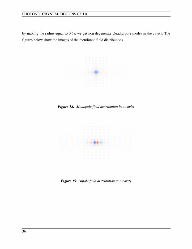
by making the radius equal to 0.6a, we get non degenerate Quadra pole modes in the cavity. The
figures below show the images of the mentioned field distributions.
Figure 18: Monopole field distribution in a cavity
Figure 19: Dipole field distribution in a cavity

SIMULATIONS OF PHOTONIC CRYSTAL DEVICES
37
Figure 20: Quadra-pole field distribution in a cavity
7.3 Ultra-High Line Modulated Cavity:
We present an ultrahigh quality factor (Q) photonic crystal slab nanocavity formed by the
local width modulation of a line defect, which is given in [8][9]. We show that only shifting two
holes away from a line defect is enough to attain an ultrahigh Q value.
The authors in their paper named “Ultrahigh-Q photonic crystal nanocavities realized by the
local width modulation of a line defect” have designed a triangular photonic crystal to achieve a
high Q-factor. They use a double hetero structure approach here. They design a cavity by putting
a line defect in the crystal, and then they shift the lattice points through different distances as
shown in the figure.
The lattice constant of the crystal is 420nm, Slab index is 3.46 (Si), the radius of the air
holes is 108nm and the holes are shifted by a distance x, 2x/3, x/3 respectively. The width of the
line defect is 0.98W.

PHOTONIC CRYSTAL DESIGNS (PCD)
38
Figure 21: Triangular photonic crystal cavity
Through this structure they get the high value of Q-factor, which is 7 x 10⁷, at a lattice shift of
9nm.
7.3.1 Results:
We design exactly the same structure given below by making air holes in a high index
region of 3.46 in a triangular form.

SIMULATIONS OF PHOTONIC CRYSTAL DEVICES
39
Figure 22: Proposed structure of the Triangular Photonic crystal cavity
In order to get the frequency of the light we make a band structure of this photonic crystal
because we have given the radius of the air holes so we have made its band diagram.

PHOTONIC CRYSTAL DESIGNS (PCD)
40
Figure 23: Band diagram of Triangular Photonic Crystal
In the band diagram, we found two band gaps, one from 0.2 to 0.26 and the other is from
0.41 to 0.46. So from here we get the center frequency about 0.215.
As this is a triangular photonic crystal, so the band gap is formed for the TE modes. A very
small or no band gap will be formed for the TM modes. So here we have assumed it for the TE
modes in which the E-field is in the crystal plan and the H-field is in the perpendicular direction.
From the above calculations we get the frequency of the light = 0.215, the size of the source
(2 0) and the position of the plane wave source (0 4). The crystal is placed in the xy plane and its
dimensions are 12 x 16. So by using these values we get the Q-factor = 4108.4 × . The figure
below shows the formation of the double heterostructure nano cavity in the crystal.

SIMULATIONS OF PHOTONIC CRYSTAL DEVICES
41
Figure 24: Field view of a double heterostructure nano cavity
7.3.2 Discussion:
The Q-factor we got over here is 4108.4 × which is less than 7 x 10⁷. The reason for this is
that, that we do not know exactly some of the important parameters given below.
1) We do not know the position of the plane wave source.
2) We do not know the size of the plane wave source.
3) We do not know the frequency of the light.
4) We do not know about the polarization of light.
The crystal which we use over here to design a double heterostructure nano cavity is a triangular
photonic crystal. We draw the band structure for this crystal by using brillouin zone as shown in
the figure below. This brillouin zone is large enough, we do not need to go inside of it, we will
just travel at its edges. So for that we will draw a triangle inside of it. This triangle is called the
irreducible brillouin zone. If we rotate this triangle, than we can construct the whole brillouin
zone. When we move from Γ to K, K to M and from M to Γ than the first band will be formed,
than the second band and so on as shown in the band structure diagram given above. The bands
PHOTONIC CRYSTAL DESIGNS (PCD)
42
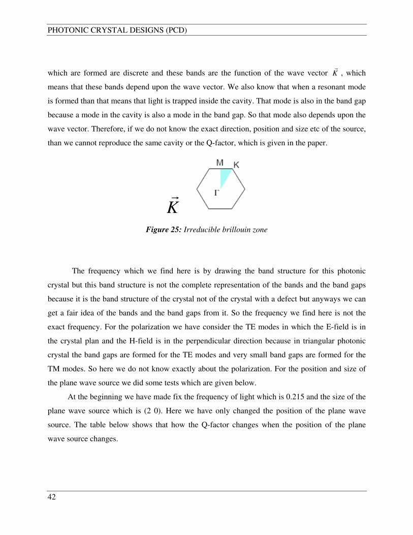
which are formed are discrete and these bands are the function of the wave vector Kr
, which
means that these bands depend upon the wave vector. We also know that when a resonant mode
is formed than that means that light is trapped inside the cavity. That mode is also in the band gap
because a mode in the cavity is also a mode in the band gap. So that mode also depends upon the
wave vector. Therefore, if we do not know the exact direction, position and size etc of the source,
than we cannot reproduce the same cavity or the Q-factor, which is given in the paper.
Kr
Figure 25: Irreducible brillouin zone
The frequency which we find here is by drawing the band structure for this photonic
crystal but this band structure is not the complete representation of the bands and the band gaps
because it is the band structure of the crystal not of the crystal with a defect but anyways we can
get a fair idea of the bands and the band gaps from it. So the frequency we find here is not the
exact frequency. For the polarization we have consider the TE modes in which the E-field is in
the crystal plan and the H-field is in the perpendicular direction because in triangular photonic
crystal the band gaps are formed for the TE modes and very small band gaps are formed for the
TM modes. So here we do not know exactly about the polarization. For the position and size of
the plane wave source we did some tests which are given below.
At the beginning we have made fix the frequency of light which is 0.215 and the size of the
plane wave source which is (2 0). Here we have only changed the position of the plane wave
source. The table below shows that how the Q-factor changes when the position of the plane
wave source changes.

SIMULATIONS OF PHOTONIC CRYSTAL DEVICES
43
Position of the Plane Wave Source Quality Factor
0 297.194
1 85.66
1.5 113
2 1171
2.5 221
3 110
3.5 411
3.999 123
4 48000
4.001 395
4.5 168
5 126
5.5 82
6 77
Table 7.1: Position of the plane wave source and the quality factor
The graph below shows the complete picture of the position of the plane wave source
verses the quality factor. So according to the graph we get the high Q-factor when the source is at
the position (0 4).
PHOTONIC CRYSTAL DESIGNS (PCD)
44
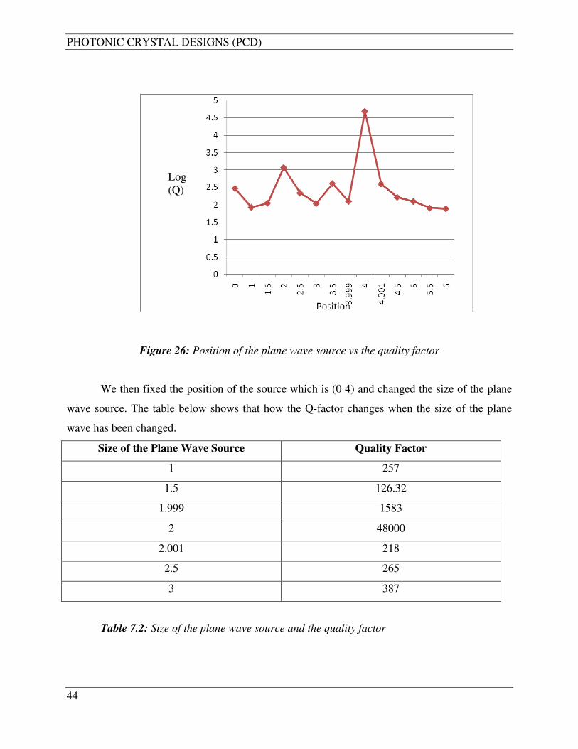
Figure 26: Position of the plane wave source vs the quality factor
We then fixed the position of the source which is (0 4) and changed the size of the plane
wave source. The table below shows that how the Q-factor changes when the size of the plane
wave has been changed.
Size of the Plane Wave Source Quality Factor
1 257
1.5 126.32
1.999 1583
2 48000
2.001 218
2.5 265
3 387
Table 7.2: Size of the plane wave source and the quality factor
Log
(Q)

SIMULATIONS OF PHOTONIC CRYSTAL DEVICES
45
The graph below shows the complete picture of the size of the plane wave source verses
the quality factor. So according to the graph we get the high quality factor when the source size is
(2 0).
Figure 27: Size of the plane wave source vs the quality factor
We have also tried different light frequencies. We have made fix the size (2 0) and
position (0 4) of the plane wave source and change frequencies. The table below shows how the
Q-factor changes when the frequency of the light changes.
Log
(Q)

PHOTONIC CRYSTAL DESIGNS (PCD)
46
Frequency of Plane wave source Quality Factor
0.2 69
0.212 3
0.213 92
0.214 166
0.215 48000
0.216 6
0.217 201
0.218 112
0.219 4
0.22 23
0.221 3
0.222 53
0.223 1095
0.224 2
0.225 255
0.226 59
0.227 145
0.228 74
0.229 61
Table 7.3: Frequency of the plane wave source and the quality factor
The graph below shows the complete picture of the frequency of light verses the Q-factor.

47
Figure 28: Frequency of the light vs the quality factor
Log
(Q)

PHOTONIC CRYSTAL DESIGNS (PCD)
48
CONCLUSION
The explanation of the Maxwell’s curl equations offers classical electromagnetic
phenomenon, for time varying fields. Maxwell originated the four of the most basic equations of
electromagnetic theory, which engineers and scientists exploit worldwide.
FDTD (Finite Difference Time Domain) is a numerical technique requiring very high
computational power, but with the development of fast computers has made this method growing
famous in the electromagnetic area.
We have shown that photonic crystals can be used for the production of high-Q micro
cavities. By set up a defect in a photonic crystal, intense resonant states can be formed in the area
of the defect. The properties of these modes like the frequency, polarization, symmetry, and field
distribution, can be controlled by varying the nature and the size of the defect. Furthermore, we
offer an ultrahigh quality factor (Q) photonic crystal slab nanocavity formed by the local width
modulation of a line defect. We show that only shifting two holes away from a line defect is
enough to attain an ultrahigh Q value. The Q-factor we got is 4108.4 × , which is less than
7107 × . The reason for this is that, that we do not know the exact frequency, polarization, size,
direction and position of the plane wave source. If we know exactly these parameters, than we
can get the high Q-factor. Nobody has designed the double heterostructure nano cavity in MIT
Electromagnetic Equation Propagation (MEEP) software. This software has additional features
like the sub pixel averaging, boundary conditions and symmetries etc.
Scientists and engineers will work on these double heterostructure nano cavities to get the
higher Q-value, which will be used to design the micro and nano lasers. The only problem in the
photonic crystal cavities is that, that they are very sensitive to frequency, polarization, size and
position of the source. So we should choose the right values for these parameters and should be
very careful to design such devices.

REFERENCES
49
REFERENCES
[1] J. D. Joannopoulos, Steven G.Johnson, Joshua N. Winn and Robert D.Meade,
Photonic Crystals – Modeling the Flow of Light. 2nd
Edition, Princeton University
Press, ISBN: 978-0-691-12456-8.
[2] Steven G. Johnson and J. D. Joannopoulos, Introduction to Photonic Crystals:
Bloch’s Theorem, Band Diagrams and Gaps (but no Defects), MIT 3rd
February
2003.
[3] Http://ab-initio.mit.edu/wiki/index.php/meep, April 2009.
[4] Attila Mekis, J. C. Chen, I. Kurland, Shanhui Fan, Pierre R. Villeneuve, and J.
D.Joannopoulos - High Transmission through Sharp Bends in Photonic Crystal
Waveguides, Volume 77, Number 18, October 1996.
[5] Christopher L. Wagner - Theoretical basis for numerically exact three-dimensional
time- domain algorithms, Journal of Computational Physics, Volume 205, Issue 1,
May 2005.
[6] Kurt l. Shlager and John B. Schneider “A selective survey of the finite-difference
time-domain literature” IEEE antennas and propagation magazine, Volume 37,
issue 4, Aug 1995.
[7] Sun-Goo Lee, Sang Soon Oh, Jae-Eun Kim, and Hae Yong Parka, Department of
Physics, Korea Advanced Institute of Science and Technology, “Line-defect
Induced bending and splitting of self-collimated beams in two-dimensional
Photonic crystals”, Received 20 June 2005; accepted 14 September 2005;
published online 26 October 2005.
[8] Eiichi Kuramochi,a Masaya Notomi, Satoshi Mitsugi,Akihiko Shinya, Takasumi
Tanabe, NTT Basic Research Laboratories, NTT Corporation, Ats Kanagawa
243-0198, Japan, “Ultrahigh-Q photonic crystal nanocavities realized by the local
width modulation of a line defect”, Published 24 January 2006.
[9] M. Notomi, E. Kuramochi, H. Taniyama. NTT Basic Research Laboratories, NTT
Corporation, Atsugi, Kanagawa 243-0198, Japan, “Ultrahigh-Q Nanocavity with
1D Photonic Gap”, Published 21 July 2008 / Vol. 16, No. 15 / Optics Express
11095.
[10] Bong-Shik Song, Takashi Asano and Susumu Noda. Department of Electronic
Science and Engineering, Kyoto University, Japan, “Physical origin of the small
modal volume of ultra-high-Q photonic double-heterostructure nanocavities,
Published 14 May 2006.
[11] http://physicsworld.com/cws/article/print/530, 1st august 2000.
[12] S. Y. Lin and Edmond Chow, S. G. Johnson and J. D. Joannopoulos, Direct
measurement of the quality factor in a two-dimensional photonic-crystal
microcavity. Vol. 26, No. 23, December 2001.
[13] Cui Xudong, Christian Hafner, Rüdiger Vahldieck, Franck Robin, Laboratory
for Electromagnetic Fields and Microwave Electronics, ETH, “Sharp trench
waveguide bends in dual mode operation with ultra-small photonic crystals for
suppressing radiation”, Vol. 14, Issue 10, Optics Express.

PHOTONIC CRYSTAL DESIGNS (PCD)
50
[14] Cazimir G. Bostan and René M. de Ridder. University of Twente,
MESA+Research Institute, Integrated Optical MicroSystems (IOMS) group,
“Design of Waveguides, Bends and Splitters in Photonic Crystal Slabs with
Hexagonal Holes in a Triangular Lattice”, IEEE, ICTON , Vol. 1, July 2005.
[15] Naoyuki FUKAYA, Daisuke OHSAKI and Toshihiko BABA, Yokohama
National University, Faculty of Engineering, Division of Electrical and
Computer Engineering,“ Two-Dimentional Photonic Crystal Waveguide with 60
degree Bends in a Thin Slab Structure”, Jpn. J. Appl. Phys. Vol. 39(2000) pp.
2619-2623.
[16] David Roundy, Mihai Ibanescu and Peter Bermel - MIT Electromagnetic
Equation Propogation, March 1, 2005.
[17] Eli Yablonovitch, “Photonic crystals: Semiconductor s of light,” Scientific
American, Vol. 285, No. 6, pp. 47-55, Dec. 2001.
[18] Pierre R. Villeneuve, Shanhui Fan, and J. D. Joannopoulos, Department of
Physics Massachusetts Institute of Technology, “Microcavities in photonic
crystals: Mode symmetry, tunability, and coupling efficiency”, Vol. 54, No. 11.