Makerspace microfabrication of a stainless steel 3D ...
11
Makerspace microfabrication of a stainless steel 3D microneedle electrode array (3D MEA) on a glass substrate for simultaneous optical and electrical probing of electrogenic cells Paola M. Morales-Carvajal, † a Avra Kundu, † a Charles M. Didier, ab Cacie Hart, ac Frank Sommerhage a and Swaminathan Rajaraman * abcd Microfabrication and assembly of a Three-Dimensional Microneedle Electrode Array (3D MEA) based on a glass-stainless steel platform is demonstrated involving the utilization of non-traditional “Makerspace Microfabrication” techniques featuring cost-effective, rapid fabrication and an assorted biocompatible material palette. The stainless steel microneedle electrode array was realized by planar laser micromachining and out-of-plane transitioning to have a 3D configuration with perpendicular transition angles. The 3D MEA chip is bonded onto a glass die with metal traces routed to the periphery of the chip for electrical interfacing. Confined precision drop casting (CPDC) of PDMS is used to define an insulation layer and realize the 3D microelectrodes. The use of glass as a substrate offers optical clarity allowing for simultaneous optical and electrical probing of electrogenic cells. Additionally, an interconnect using 3D printing and conductive ink casting has been developed which allows metal traces on the glass chip to be transitioned to the bottomside of the device for interfacing with commercial data acquisition/analysis equipment. The 3D MEAs demonstrate an average impedance/phase of 13.3 kU/12.1 at 1 kHz respectively, and an average 4.2 mV noise. Lastly, electrophysiological activity from an immortal cardiomyocyte cell line was recorded using the 3D MEA demonstrating end to end device development. 1. Introduction Cells have a membrane potential that is the basis for inte- grating, generating, driving and transmitting signals from the cells to the external environment. 1 Changes in ionic perme- ability translate into the electrical activity that regulates cellular physiology. Phenomena such as the potential from cardiac action, neurotransmission and production of neurotransmit- ters, cell proliferation, activation and differentiation, ion transport and the release of hormones are all based on electrical activity. 2 Cellular electrophysiology is the study of the electrical properties of biological cells and tissues and the interpretation of this activity. 3,4 Microelectrode arrays are one of the primary interfaces used to record and stimulate electrical activity from the in vitro electrogenic cell cultures and serve as label-free platforms in the pharmaceutical industry to provide informa- tion for instance about a drug's efficacy. 5 Microelectrode arrays have become vital in different elds such as pharmacology, toxicology, high throughput screening, stem cell differentiation etc. to obtain in vitro electrical measurements of different clusters of neurons, cells, tissues, etc. 6 Microelectrode arrays are increasingly being used for “disease-on-a-chip” models for neural diseases such as Parkinson's, epilepsy, Amyotrophic Lateral Sclerosis (ALS), neuropathic pain, and autism spectrum disorders. 5 MEAs can therefore perform clinically relevant nerve conduction tests and measure changes in electrophysiological properties that reect the effects on the human nervous system. Microelectrode arrays are additionally used in cardiac applications, for instance in cardiac cell therapeutics or to improve the existing cardiac safety mechanisms. 7 Microelec- trode arrays serve as a platform to evaluate arrhythmia risk and such studies are vital to understanding the complex and varied nature of arrhythmia. 8 Microelectrode array technology plays an important role in advancing human health by pushing the boundaries of disease modeling and therapeutics including drug discovery along with safety and toxicology studies. Conventional microelectrode arrays are planar (2D) in nature and typically fabricated in state of the art cleanroom facilities. 7,9 a NanoScience Technology Center (NSTC), University of Central Florida, 4353 Scorpius Street, Orlando, FL 32816-0120, USA. E-mail: [email protected]; Tel: +1-407-823-4339 b Burnett School of Biomedical Sciences, University of Central Florida, Orlando, FL 32827, USA c Department of Materials Science & Engineering, University of Central Florida, Orlando, FL 32826, USA d Department of Electrical & Computer Engineering, University of Central Florida, Orlando, FL 32826, USA † Contributed equally to the paper. Cite this: RSC Adv. , 2020, 10, 41577 Received 11th July 2020 Accepted 6th October 2020 DOI: 10.1039/d0ra06070d rsc.li/rsc-advances This journal is © The Royal Society of Chemistry 2020 RSC Adv. , 2020, 10, 41577–41587 | 41577 RSC Advances PAPER Open Access Article. Published on 18 November 2020. Downloaded on 11/10/2021 12:01:58 AM. This article is licensed under a Creative Commons Attribution-NonCommercial 3.0 Unported Licence. View Article Online View Journal | View Issue
Transcript of Makerspace microfabrication of a stainless steel 3D ...

RSC Advances
PAPER
Ope
n A
cces
s A
rtic
le. P
ublis
hed
on 1
8 N
ovem
ber
2020
. Dow
nloa
ded
on 1
1/10
/202
1 12
:01:
58 A
M.
Thi
s ar
ticle
is li
cens
ed u
nder
a C
reat
ive
Com
mon
s A
ttrib
utio
n-N
onC
omm
erci
al 3
.0 U
npor
ted
Lic
ence
.
View Article OnlineView Journal | View Issue
Makerspace micr
aNanoScience Technology Center (NSTC), Un
Street, Orlando, FL 32816-0120, USA. E-mai
+1-407-823-4339bBurnett School of Biomedical Sciences, Un
32827, USAcDepartment of Materials Science & Engi
Orlando, FL 32826, USAdDepartment of Electrical & Computer En
Orlando, FL 32826, USA
† Contributed equally to the paper.
Cite this: RSC Adv., 2020, 10, 41577
Received 11th July 2020Accepted 6th October 2020
DOI: 10.1039/d0ra06070d
rsc.li/rsc-advances
This journal is © The Royal Society o
ofabrication of a stainless steel 3Dmicroneedle electrode array (3D MEA) on a glasssubstrate for simultaneous optical and electricalprobing of electrogenic cells
Paola M. Morales-Carvajal, †a Avra Kundu, †a Charles M. Didier, ab
Cacie Hart, ac Frank Sommerhage a and Swaminathan Rajaraman*abcd
Microfabrication and assembly of a Three-Dimensional Microneedle Electrode Array (3D MEA) based on
a glass-stainless steel platform is demonstrated involving the utilization of non-traditional “Makerspace
Microfabrication” techniques featuring cost-effective, rapid fabrication and an assorted biocompatible
material palette. The stainless steel microneedle electrode array was realized by planar laser
micromachining and out-of-plane transitioning to have a 3D configuration with perpendicular transition
angles. The 3D MEA chip is bonded onto a glass die with metal traces routed to the periphery of the chip
for electrical interfacing. Confined precision drop casting (CPDC) of PDMS is used to define an insulation
layer and realize the 3D microelectrodes. The use of glass as a substrate offers optical clarity allowing for
simultaneous optical and electrical probing of electrogenic cells. Additionally, an interconnect using 3D
printing and conductive ink casting has been developed which allows metal traces on the glass chip to
be transitioned to the bottomside of the device for interfacing with commercial data acquisition/analysis
equipment. The 3D MEAs demonstrate an average impedance/phase of �13.3 kU/�12.1� at 1 kHz
respectively, and an average 4.2 mV noise. Lastly, electrophysiological activity from an immortal
cardiomyocyte cell line was recorded using the 3D MEA demonstrating end to end device development.
1. Introduction
Cells have a membrane potential that is the basis for inte-grating, generating, driving and transmitting signals from thecells to the external environment.1 Changes in ionic perme-ability translate into the electrical activity that regulates cellularphysiology. Phenomena such as the potential from cardiacaction, neurotransmission and production of neurotransmit-ters, cell proliferation, activation and differentiation, iontransport and the release of hormones are all based on electricalactivity.2 Cellular electrophysiology is the study of the electricalproperties of biological cells and tissues and the interpretationof this activity.3,4 Microelectrode arrays are one of the primaryinterfaces used to record and stimulate electrical activity from
iversity of Central Florida, 4353 Scorpius
l: [email protected]; Tel:
iversity of Central Florida, Orlando, FL
neering, University of Central Florida,
gineering, University of Central Florida,
f Chemistry 2020
the in vitro electrogenic cell cultures and serve as label-freeplatforms in the pharmaceutical industry to provide informa-tion for instance about a drug's efficacy.5 Microelectrode arrayshave become vital in different elds such as pharmacology,toxicology, high throughput screening, stem cell differentiationetc. to obtain in vitro electrical measurements of differentclusters of neurons, cells, tissues, etc.6 Microelectrode arrays areincreasingly being used for “disease-on-a-chip” models forneural diseases such as Parkinson's, epilepsy, AmyotrophicLateral Sclerosis (ALS), neuropathic pain, and autism spectrumdisorders.5 MEAs can therefore perform clinically relevant nerveconduction tests and measure changes in electrophysiologicalproperties that reect the effects on the human nervous system.
Microelectrode arrays are additionally used in cardiacapplications, for instance in cardiac cell therapeutics or toimprove the existing cardiac safety mechanisms.7 Microelec-trode arrays serve as a platform to evaluate arrhythmia risk andsuch studies are vital to understanding the complex and variednature of arrhythmia.8 Microelectrode array technology plays animportant role in advancing human health by pushing theboundaries of disease modeling and therapeutics includingdrug discovery along with safety and toxicology studies.Conventional microelectrode arrays are planar (2D) in natureand typically fabricated in state of the art cleanroom facilities.7,9
RSC Adv., 2020, 10, 41577–41587 | 41577

RSC Advances Paper
Ope
n A
cces
s A
rtic
le. P
ublis
hed
on 1
8 N
ovem
ber
2020
. Dow
nloa
ded
on 1
1/10
/202
1 12
:01:
58 A
M.
Thi
s ar
ticle
is li
cens
ed u
nder
a C
reat
ive
Com
mon
s A
ttrib
utio
n-N
onC
omm
erci
al 3
.0 U
npor
ted
Lic
ence
.View Article Online
In order to better mimic in vivo-like conditions10,11 for in vitroapplications, 3D cell culture models are becoming increasinglypopular as they are better able to capture signaling pathwaysand drug responsiveness in disease states when compared to 2Dmodels.12–15 3D cell cultures enable the formation of dynamicand spatial gradients of soluble factors that inuence cellularmigration, better represent cell to cell communication anddifferentiation to accurately predict in vivo tissue functions anddrug response signatures.15,16 This has led to an increasing needto extend cell culture matrices and support scaffolds to the thirddimension.11 Such culture models would help realize “disease-on-a-plate” and fully functional “organ-on-a-chip” models topromote cell/tissue growth and regeneration in vitro.17
In response to the growth of 3D cellular models specicallyfor electrogenic cells, there has been a growing need to extend invitro microelectrodes to the third dimension. Three-Dimensional Microneedle Electrode Array (3D MEAs) wouldallow for simple, high throughput screening and measurementof network dynamics for the study of 3D microengineeredcellular systems including but not limited to central orperipheral nervous system applications such as the recentlydeveloped Human Nerve-on-a-Chip (HNoaC) system which is3D in nature and can be used for evaluating electrophysiologicaland histological metrics18 and other organ systems for instanceextracellular microelectrode recordings from cardiac myocytestowards in vitro heart-on-a-chip models.19 Enabling 3D func-tionality in MEAs built atop optically transparent materialswould enable simultaneous extraction of optical and electricaldata from 3D cell cultures.
Microfabrication of 3DMEAs using conventional cleanroom-based techniques is particularly challenging because most ofthe techniques are suited for two-dimensional device process-ing. These techniques have been adopted to realize the earliestinterfaces created on silicon wafers and glass coverslips.20,21
Several polymers such as polydimethylsiloxane, parylene etc.,have emerged as a newer material set for MEA fabricationproviding several advantages over traditional glass/siliconsubstrates. They not only offer simpler microfabricationmethods but also provide physical exibility, proven biocom-patibility and biostability.22,23 Additionally, backend technolo-gies such as Printed Circuit Boards (PCBs), Chip On Board(COB), and ip chip technologies have been utilized to interfacethe microfabricated devices with commercial amplicationsystems for data processing, analysis and plotting.5 Recently, 3Dprinting of photopolymeric resins have been reported to realizeMEAs having electrode densities up to a commercially popular 8� 8 array allowing for the MEAs to be “used and tossed” andmoving the manufacturing from the cleanroom to maker-spaces.24 The use of makerspace techniques compares veryfavorably with traditional glass MEAs in terms of design todevice while representing a dramatic reduction in cost, timelinefor fabrication, reduction in the number of steps and the needfor sophisticated microfabrication and packaging equipmentalong with the capability of monolithic microfabrication of thedevice and package for seamless integration with commercialdata acquisition and amplication systems.24
41578 | RSC Adv., 2020, 10, 41577–41587
In this paper, the microfabrication and packaging ofa stainless steel (SS) 3D MEA assembled on a glass substrate isreported. The device fabrication employs non-traditional“Makerspace Microfabrication”11,24,25 techniques to realize thedevice predominantly outside the cleanroom. The use of“Makerspace Microfabrication” has been demonstrated previ-ously by the authors to realize a 2D MEA up to a commerciallypopular 8 � 8 array as stated earlier.24 The present work differsfrom the earlier reported method on several fronts. First, we usedifferent toolbox technologies present in the makerspace envi-ronment to realize microneedle electrodes in 3D instead of 2Delectrodes as reported in our prior work. While the prior workrelied heavily on 3D printing to fabricate the 2D MEA, this workonly relies on 3D printing for realizing a custom jig for inter-facing the device with commercially available data acquisitionsystems. Second, the substrate presented as a part of this workis glass; a completely transparent platform suitable for theoptical interrogation (upright, confocal or inverted microscopy)of the cell culture. Third, the use of the glass platform allows forthe use of proven biocompatible materials like such as stainlesssteel, titanium, gold, polydimethylsiloxane (PDMS), poly-ethylene terephthalate glycol (PET-G) to facilitate cytocompati-bilty with cardiac and other cell lines. Lastly, we reportelectrophysiological testing in this paper. Specically, lasermicromachining is used to ablate a SS sheet with ten (10)obelisk-type microneedle geometries. Eight (8) obelisks arearranged in a linear array and the construct is terminated by two(2) obelisks adjacent to one another. The dimensions of theobelisk ablation are designed to incorporate a height of 400 mmand a width of 300 mm once it is transitioned out-of-plane tohave a 3D conguration. The pitch of the obelisk is 600 mm inthe linear portion of the array. The tip of the obelisk geometrycan additionally penetrate into prepared slices from brain andother electrogenic tissues.26 The 3D obelisk array is subse-quently assembled on a highly transparent glass chip withmetallized titanium–gold (Ti–Au) traces making the platformcapable of simultaneous optical and electrical probing. Thearray of electrodes is isolated from each other by laser micro-machining to have ten (10) individual recording/stimulationsites. Controlled precision drop-casting (CPDC) is used todene the PDMS insulation material aer affixing the PET-Gculture well onto the glass chip. Cellular electrophysiologicalactivity of HL-1 cells, a cardiac muscle cell line from the AT-1mouse was measured aer approximately 2 days in vitro (DIV).
2. Materials and methods2.1 Microfabrication of three-dimensional stainless steelmicroneedle electrode array (3D MEA)
The obelisk shaped MEA was designed using SolidWorks,Dassault Systems Inc., (Velizy-Villacoublay, France) in DrawingInterchange format (*.dxf). The length of the construct was 4200mm with a width 500 mm terminating with a circular regionhaving a diameter of 800 mm. MEA consisting of ten (10) elec-trodes were placed inside the described silhouette and a singleplanar microneedle cutout had a base width of 300 mm, lengthof 400 mm and a pitch of 600 mm. Fig. 1(a) shows the schematic
This journal is © The Royal Society of Chemistry 2020

Fig. 1 Schematic process flow for laser micromachining of 3D microneedle electrodes: (a) laser micromachining a obelisk-type geometry using1064 nm (IR) wavelength using Quick Laze 50ST2, Eolite Lasers onto a stainless steel substrate having a thickness of 25 mm; (b) transitioning thelaser micromachined area out-of-plane using a hypodermic needle and releasing the 3Dmicroneedles from the bulk stainless steel substrate bylaser micromachining at the same wavelength, 1064 nm (IR); (c) the keyhole of the released 3Dmicroneedles. The microneedle electrodes havea width of 300 mm, height of 400 mm and a pitch of 600 mm. The keyhole cutout in the stainless steel sheet is further obtained shown as inset.
Paper RSC Advances
Ope
n A
cces
s A
rtic
le. P
ublis
hed
on 1
8 N
ovem
ber
2020
. Dow
nloa
ded
on 1
1/10
/202
1 12
:01:
58 A
M.
Thi
s ar
ticle
is li
cens
ed u
nder
a C
reat
ive
Com
mon
s A
ttrib
utio
n-N
onC
omm
erci
al 3
.0 U
npor
ted
Lic
ence
.View Article Online
of the laser micromachining of the SS sheet (25 mm thick)micromachined with infrared laser wavelength (1064 nm) usingthe QuikLaze 50 ST2 laser micromachining system (EoliteLasers, Portland, OR, USA) with the close-up of the micro-machining pattern shown in the inset. The laser was operated ata repetition rate of 50 Hz with a scanning speed of 40 mm s�1.The obelisk shaped cut-outs in SS were transitioned out of planeinto a 3D conguration using a hypodermic needle [Fig. 1(b)].Fig. 1(c) shows the schematic of the 3D MEA aer it has beenreleased from the SS substrate and the inset shows the cutout inthe SS substrate which would be used in subsequent processingsteps as a shadowmask to cast silver conductive paste and bondthe MEA with the glass chip.
Fig. 2 Schematic process flow of glass chip fabrication and stainlesssteel assembly: (a) glass chip (500 mm thickness) cleaned in �2 Msolution of KOH (potassium hydroxide) in IPA (isopropyl alcohol; 2-propanol); (b) metallization of a stack of titanium–gold (30 nm–90 nm)using electron beam evaporation through a Kapton shadowmask. TheKapton shadow mask was laser micromachined using 355 nm (UV)using the same Eolite Laser; (c) the titanium–gold traces are 150 mmwide and the contact pads at the periphery of the chip are designed tobe 1 mm � 1 mm; (d) the 3D microneedle electrodes are aligned withthe metal traces and bonded using silver paste. The silver paste is castthrough the SS cutout; (e) the glass chip bonded to the 3D stainlesssteel keyhole having 10 microneedles using silver paste; (f) a PET-Gculture ring is attached using PDMS and the 3D microneedles areisolated from each other using laser micromachining (1064 nm) toyield ten (10) of 3D recording/stimulating electrodes; (g) controlledprecision drop-casting and self-planarization of PDMS to achieve theinsulation layer; (h) the volume of PDMS controls the height of thePDMS insulation in the area confined by the PET-G ring and deter-mines the geometric area of the 3D Microneedle Electrode Array(MEA); (i) HL-1 cells interacting with a singular 3D microneedleelectrode.
2.2 Assembly and packaging of the device
The SS 3D electrodes were assembled on a highly transparentglass chip (22 mm � 22 mm � 0.5 mm) to allow for simulta-neous optical and electrical probing [Fig. 2(a)]. The glasssubstrate was rst cleaned in KOH (potassium hydroxide) in IPA(isopropyl alcohol/2 propanol). The IPA allowed for a slowingdown the etch rate of glass in KOH along with enablinga smoother surface nish.27 For electrical probing from the 3DMEA, traces of (Ti; 4N5 purity pellets) and gold (Au; 5N puritypellets) (Kurt J. Lesker, Jefferson Hills, PA, USA) were depositedby electron-beam (E-beam) evaporation (Thermionics Labora-tory Inc., Port Townsend, WA, USA) through a shadow maskfabricated out of Kapton®. The shadow mask design hadprobing pads in place for vias of the 3D printed frame, whichwas retrotted on to the glass chip [Section 2.3]. The traces andprobing pads for the shadow mask were designed in Solid-Works. The traces are designed to be 150 mm wide and �7–16 mm long depending upon the position of the electrode andthe pad. The dimension of the probing pads was 1 � 1 mm witha pitch of 4 mm. The Kapton® mask was ablated with a Qui-kLaze 50 ST2 laser micromachining system (Eolite Lasers,Portland, OR, USA) (UV wavelength: 355 nm, scanning speed of70 mm s�1, repetition rate: 50 Hz) [Fig. 2(b)] prior to themetallization [Fig. 2(c)]. Subsequently, the SS keyhole cutout
This journal is © The Royal Society of Chemistry 2020
mask [inset of Fig. 1(c)] was placed on top of the glass chip andaligned with the central region of the glass chip [Fig. 2(c)] andthe 3D MEA was bonded to the glass substrate with silver
RSC Adv., 2020, 10, 41577–41587 | 41579
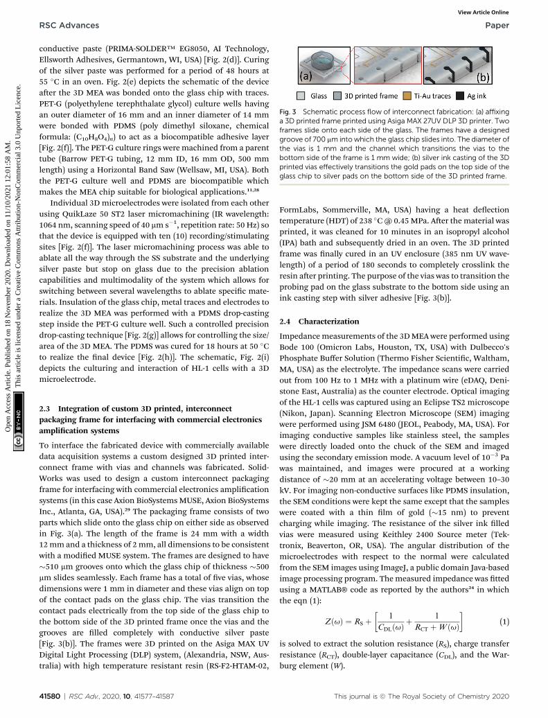
Fig. 3 Schematic process flow of interconnect fabrication: (a) affixinga 3D printed frame printed using Asiga MAX 27UV DLP 3D printer. Twoframes slide onto each side of the glass. The frames have a designedgroove of 700 mm into which the glass chip slides into. The diameter ofthe vias is 1 mm and the channel which transitions the vias to thebottom side of the frame is 1 mm wide; (b) silver ink casting of the 3Dprinted vias effectively transitions the gold pads on the top side of theglass chip to silver pads on the bottom side of the 3D printed frame.
RSC Advances Paper
Ope
n A
cces
s A
rtic
le. P
ublis
hed
on 1
8 N
ovem
ber
2020
. Dow
nloa
ded
on 1
1/10
/202
1 12
:01:
58 A
M.
Thi
s ar
ticle
is li
cens
ed u
nder
a C
reat
ive
Com
mon
s A
ttrib
utio
n-N
onC
omm
erci
al 3
.0 U
npor
ted
Lic
ence
.View Article Online
conductive paste (PRIMA-SOLDER™ EG8050, AI Technology,Ellsworth Adhesives, Germantown, WI, USA) [Fig. 2(d)]. Curingof the silver paste was performed for a period of 48 hours at55 �C in an oven. Fig. 2(e) depicts the schematic of the deviceaer the 3D MEA was bonded onto the glass chip with traces.PET-G (polyethylene terephthalate glycol) culture wells havingan outer diameter of 16 mm and an inner diameter of 14 mmwere bonded with PDMS (poly dimethyl siloxane, chemicalformula: (C10H8O4)n) to act as a biocompatible adhesive layer[Fig. 2(f)]. The PET-G culture rings were machined from a parenttube (Barrow PET-G tubing, 12 mm ID, 16 mm OD, 500 mmlength) using a Horizontal Band Saw (Wellsaw, MI, USA). Boththe PET-G culture well and PDMS are biocompatible whichmakes the MEA chip suitable for biological applications.11,28
Individual 3D microelectrodes were isolated from each otherusing QuikLaze 50 ST2 laser micromachining (IR wavelength:1064 nm, scanning speed of 40 mm s�1, repetition rate: 50 Hz) sothat the device is equipped with ten (10) recording/stimulatingsites [Fig. 2(f)]. The laser micromachining process was able toablate all the way through the SS substrate and the underlyingsilver paste but stop on glass due to the precision ablationcapabilities and multimodality of the system which allows forswitching between several wavelengths to ablate specic mate-rials. Insulation of the glass chip, metal traces and electrodes torealize the 3D MEA was performed with a PDMS drop-castingstep inside the PET-G culture well. Such a controlled precisiondrop-casting technique [Fig. 2(g)] allows for controlling the size/area of the 3D MEA. The PDMS was cured for 18 hours at 50 �Cto realize the nal device [Fig. 2(h)]. The schematic, Fig. 2(i)depicts the culturing and interaction of HL-1 cells with a 3Dmicroelectrode.
2.3 Integration of custom 3D printed, interconnectpackaging frame for interfacing with commercial electronicsamplication systems
To interface the fabricated device with commercially availabledata acquisition systems a custom designed 3D printed inter-connect frame with vias and channels was fabricated. Solid-Works was used to design a custom interconnect packagingframe for interfacing with commercial electronics amplicationsystems (in this case Axion BioSystemsMUSE, Axion BioSystemsInc., Atlanta, GA, USA).29 The packaging frame consists of twoparts which slide onto the glass chip on either side as observedin Fig. 3(a). The length of the frame is 24 mm with a width12mm and a thickness of 2 mm, all dimensions to be consistentwith a modied MUSE system. The frames are designed to have�510 mm grooves onto which the glass chip of thickness �500mm slides seamlessly. Each frame has a total of ve vias, whosedimensions were 1 mm in diameter and these vias align on topof the contact pads on the glass chip. The vias transition thecontact pads electrically from the top side of the glass chip tothe bottom side of the 3D printed frame once the vias and thegrooves are lled completely with conductive silver paste[Fig. 3(b)]. The frames were 3D printed on the Asiga MAX UVDigital Light Processing (DLP) system, (Alexandria, NSW, Aus-tralia) with high temperature resistant resin (RS-F2-HTAM-02,
41580 | RSC Adv., 2020, 10, 41577–41587
FormLabs, Sommerville, MA, USA) having a heat deectiontemperature (HDT) of 238 �C@ 0.45 MPa. Aer the material wasprinted, it was cleaned for 10 minutes in an isopropyl alcohol(IPA) bath and subsequently dried in an oven. The 3D printedframe was nally cured in an UV enclosure (385 nm UV wave-length) of a period of 180 seconds to completely crosslink theresin aer printing. The purpose of the vias was to transition theprobing pad on the glass substrate to the bottom side using anink casting step with silver adhesive [Fig. 3(b)].
2.4 Characterization
Impedancemeasurements of the 3DMEA were performed usingBode 100 (Omicron Labs, Houston, TX, USA) with Dulbecco'sPhosphate Buffer Solution (Thermo Fisher Scientic, Waltham,MA, USA) as the electrolyte. The impedance scans were carriedout from 100 Hz to 1 MHz with a platinum wire (eDAQ, Deni-stone East, Australia) as the counter electrode. Optical imagingof the HL-1 cells was captured using an Eclipse TS2 microscope(Nikon, Japan). Scanning Electron Microscope (SEM) imagingwere performed using JSM 6480 (JEOL, Peabody, MA, USA). Forimaging conductive samples like stainless steel, the sampleswere directly loaded onto the chuck of the SEM and imagedusing the secondary emission mode. A vacuum level of 10�3 Pawas maintained, and images were procured at a workingdistance of �20 mm at an accelerating voltage between 10–30kV. For imaging non-conductive surfaces like PDMS insulation,the SEM conditions were kept the same except that the sampleswere coated with a thin lm of gold (�15 nm) to preventcharging while imaging. The resistance of the silver ink lledvias were measured using Keithley 2400 Source meter (Tek-tronix, Beaverton, OR, USA). The angular distribution of themicroelectrodes with respect to the normal were calculatedfrom the SEM images using ImageJ, a public domain Java-basedimage processing program. Themeasured impedance was ttedusing a MATLAB® code as reported by the authors24 in whichthe eqn (1):
ZðuÞ ¼ RS þ�
1
CDLðuÞ þ1
RCT þW ðuÞ�
(1)
is solved to extract the solution resistance (RS), charge transferresistance (RCT), double-layer capacitance (CDL), and the War-burg element (W).
This journal is © The Royal Society of Chemistry 2020

Paper RSC Advances
Ope
n A
cces
s A
rtic
le. P
ublis
hed
on 1
8 N
ovem
ber
2020
. Dow
nloa
ded
on 1
1/10
/202
1 12
:01:
58 A
M.
Thi
s ar
ticle
is li
cens
ed u
nder
a C
reat
ive
Com
mon
s A
ttrib
utio
n-N
onC
omm
erci
al 3
.0 U
npor
ted
Lic
ence
.View Article Online
2.5 Cardiac cell culture
The electrogenic HL-1 cell line was cultured onthe microfabricated and assembled 3D MEA to determine thedevice's ability to capture electrophysiological activity. HL-1cells are immortalized mouse atrial cardiomyocytes thatcontinuously divide and spontaneously contract in culture,while maintaining a differentiated adult cardiac phenotype.30
Prior to cell culture, the MEA were sterilized using an isopropylalcohol wash for 30 minutes. The MEA were subsequentlycoated with a gelatin/bronectin extracellular matrix solutionand incubated for 12 hours to encourage the cells to adhere tothe MEA surface. Cells were initially cultured in cell cultureask (T25 Fisher Scientic) with supplemented Claycombmedium (Sigma-Aldrich, St. Louis, MO; 51800C-500ML) andpassaged following a standard procedure when they reachedconuency (approximately 48 hours). Cells were then countedusing a standard hemocytometer protocol with trypan blue(Gibco, Waltham, MA). Approximately, 31 000 cells weresubsequently seeded onto the MEA and incubated at 37 �C with5% CO2. Supplemented Claycomb cellular media was changedevery day. On the 3D MEAs in which the cells reached conu-ence and began to produce visible beating between 2–4 DIV(days in vitro), electrophysiological measurements were per-formed by interfacing the device with the Axion BioSystemsMUSE electrophysiological measurement system aer 2 DIV.Spiking activity 6 times above the root mean square (RMS) noiseof the system were recorded as action potentials.
3. Results and discussions3.1 Microfabrication of three-dimensional stainless steelmicroneedle electrode array (MEA)
Fig. 4(a) shows the SEM images of the 3D MEA aer it has beentransitioned out-of-plane using a hypodermic needle. Fig. 4(b)shows a close up SEM image of the 3D MEA. The individual 3Dmicroelectrodes were perpendicular with respect to the hori-zontal. A box plot of the angular tilt of the 3D MEA is furtherdepicted in Fig. 4(c) emphasizing the consistency of angles ofevery single microelectrode with respect to the horizontal. Fora total of 10 electrodes, the maximum angle of tilt was 90� witha minimum of 86�. An average value of 89� with respect to thehorizontal was obtained for the 3D microelectrodes. Sucha consistent angle was repeatable across multiple 3D MEAs.Fig. 4(d) depicts an SEM image of the 3D MEA bonded to theglass substrate using silver paste aer laser isolation of the ten(10) recording/stimulating sites. Fig. 4(e) shows a close up SEMimage depicting the scribe lines of the laser to isolate themicroneedles of the electrode array. Fig. 4(f) depicts an SEMimage of the completed 3DMEA aer controlled precision drop-casting process using PDMS insulation. The CPDC techniqueyields a PDMS insulation having a thickness of �250 mm. TheCPDC process can further be optimized to realize 3D electrodesof varying sizes as the PDMS casting is performed aer affixingthe Polyethylene Terephthalate Glycol (PET-G) culture well ontothe glass chip which restricts the insulation material (PDMS)within the connes of the culture well. It is observed that the
This journal is © The Royal Society of Chemistry 2020
CPDC technique insulates the entire device and exposes the SStips at a height of�400 mm to realize the 3DMEA as observed inthe inset of Fig. 4(f). SEM images of 3D microelectrodes depic-ted in gure [Fig. 4(b–d)] represents fabricated device dimen-sions of 400 mm height, 300 mm width (N ¼ 10 in an array) ata pitch of 600 mm which is as per the design dimensions. Wehave also carried out analysis of the angular tilt of the 3Dmicroelectrodes aer the CPDC step to delve into the effect ofthe insulation strategy on the geometry of the nished device. Itis observed that the angular tilt of the 3D microelectrodesremains �88.1� (Mean of N ¼ 10) aer CPDC [Fig. 4(g)] which isidentical to �89� (Mean of N ¼ 10), which was obtained for theangular tilt of the 3D MEA before CPDC. This nding is attrib-uted to the mechanical stiffness of the SS material and highlyfavorable method of CPDC. The simple pour-planarize-curetechnique does not induce any stress on the 3D MEAs andtherefore the angular tilt remains almost constant. Also, thespacing between the tips of the 3D microelectrodes has beenplotted for measuring the uniformity across the 3D MEA. It isobserved that the spacing between the tips remain extremelyclose (593 mm [average of N ¼ 7] before CPDC and 595.5 mm[average of N ¼ 7] aer CPDC as depicted in Fig. 4(h) and (i)respectively) to the expected value of the pitch of 600 mmbetween the electrodes in spite of some microneedles makingacute angles with the horizontal. This may be explained asfollows: if we assume that a single 3D microelectrode is havinganother 3D microelectrode on its either side and the anked 3Dmicroelectrode makes an acute angle with the horizontal, thetip spacing is reduced from the neighboring 3D microelectrodewhile it is increased with respect to the other neighbor. Thiscauses the mean spacing between the 3D microelectrodes toremain close to the design pitch of 600 mm. Thus, it may beconcluded that the CPDC does not interfere with the tip spacingand parallelism of the nished device.
Fig. 5 show the photomicrographs of the device fabricationand assembly in various stages during the realization of the 3DMEA. Fig. 5(a) shows the photomicrograph of the Ti–Au tracesas obtained aer e-beam evaporation through the laser micro-machined Kapton® shadow mask. Fig. 5(b) depicts the photo-micrograph of the device aer the 3D MEA is bonded to theglass substrate using the silver paste. The 3D MEA is subse-quently laser micromachined to isolate individual 3D micro-electrodes from each other and insulation of the traces andMEA is achieved using PDMS CPDC inside the PET-G culturewell to yield the assembled device [Fig. 5(c)]. Fig. 5(d) detailsa photomicrograph of the device with the 3D printed framesattached on both sides of the glass chip to realize the nalpackaged device. Fig. 5(e) portrays a close-up image of the 3Dprinted frame with the vias which can be subsequently lledwith silver paste to transition the gold probing pads on the glasschip to the bottom side of the 3D printed frame with the help ofthe ink-cast via on the outer rim of the 3D printed frame[Fig. 5(f)].
It may be noted here that the microfabrication and assemblyprocess is not only rapid but allows for several other advantagesover conventional fabrication of 3D MEAs. A technologicalsummary comparing our approach with some recent
RSC Adv., 2020, 10, 41577–41587 | 41581

Fig. 4 SEM images of the obelisk-type 3D microneedles after each of the microneedles have been transitioned out-of-plane. The keyholepattern has not been released from the stainless steel substrate as observed in (a). The close-up SEM images of the 3D microneedles is shown in(b); (c) box plot of the angle of tilt for the 3D microneedles transitioned out-of-plane after laser micromachining (N ¼ 10); (d) SEM image of thelaser scribed keyhole array to define 10 individual 3D microneedle electrodes. (e) A close-up SEM image shows the laser scribe lines and the 3Dmicroneedle resting on a layer of silver paste; (f) SEM image of the PDMS insulated 3D MEA. PDMS insulates the traces and the planar portions ofthe device to yield the recording/stimulating sites at a height of �400 mm. Close-up of a singular 3D microneedle electrode is shown as an inset.(g) Box plot of the angle of tilt for the 3D microelectrodes transitioned out-of-plane after laser micromachining and CPDC (N ¼ 10). (h) Box plotof the tip spacing between the 3D microelectrodes transitioned out-of-plane after laser micromachining (N ¼ 7). (i) Box plot of the tip spacingbetween the 3D microelectrodes transitioned out-of-plane after laser micromachining and CPDC (N ¼ 7).
RSC Advances Paper
Ope
n A
cces
s A
rtic
le. P
ublis
hed
on 1
8 N
ovem
ber
2020
. Dow
nloa
ded
on 1
1/10
/202
1 12
:01:
58 A
M.
Thi
s ar
ticle
is li
cens
ed u
nder
a C
reat
ive
Com
mon
s A
ttrib
utio
n-N
onC
omm
erci
al 3
.0 U
npor
ted
Lic
ence
.View Article Online
technologies31,32 is conducted in Table 1, where it is observedthat laser micromachining and additive manufacturing basedmakerspace microfabrication approach compares favorablywith other approaches in environment, number of processsteps, time, cost and equipment/materials.
3.2 Electrical characterization
Full spectrum impedance measurements of the 3D MEA weremeasured in Dulbecco's Phosphate Buffer Solution, (1�,Thermo Fisher Scientic, Waltham, MA, USA). Fig. 6(a) and (b)show the impedance spectra of the 3D MEA aer they wereassembled (without interconnect frame) and packaged, i.e. aerattachment of the interconnect frame (average of N ¼ 3 elec-trodes for both combinations). The measured values were ttedwith Randles' equivalent circuit model [Fig. 6(c)], a commonimpedance model used for microelectrodes.33,34 Both these datasets are very similar depicting minimal change from 3D MEAfabrication on the glass substrate to packaging with the 3Dprinted frame. The microfabricated 3D MEA having an area of
41582 | RSC Adv., 2020, 10, 41577–41587
�0.03 mm2 demonstrates an impedance and phase of �6.9 kUand �12.3� at an electrophysiological relevant frequency of 1kHz. For the packaged device the real part of the averageimpedance was 13.3 kU with phase of �12.1� at 1 kHz. Thesevalues were found to be identical to other reports in literaturefor similar sized microelectrodes.11,24,35
Further, from the extracted parameters [Table 2] it isobserved that the 3D printed frame does not affect the perfor-mance of the 3D MEA, especially for the values of the doublelayer capacitance (CDL) and Rs which remain unaltered.Changes in charge transfer resistance (RCT) and the Warburgelement were additionally observed to be within expectedlimits.24,36–38 This was attributed to the low DC resistance of thesilver ink casted vias in the 3D printed frame. Fig. 6(d) portraysa box plot of the measured resistance of vias (N¼ 10). The meanresistance of this set of vias was 3.99 U. The differences inresults were less than �1.00 U when compared to the mean.This value was found to be similar across multiple devices.
This journal is © The Royal Society of Chemistry 2020

Fig. 5 Optical photomicrographs of the fully assembled device: (a) glass chip with Ti–Au metal traces and pads; (b) photomicrograph of thedevice after the 3Dmicroneedles are bonded to the glass substrate using silver paste and subsequently laser micromachined to be isolated fromeach other as depicted in (c); (d) fully assembled device with the 3D printed frame slid onto the glass chip; (e) close up image of the 3D printed viashowing themetallized gold pad aligned with the vias on the 3D printed frame; (f) ready-to-interface device with the vias filled with silver paste sothat the gold traces on the top side of the glass chip transitions to the bottom side of the packaged device.
Table 1 Technological summary of the microfabrication development between makerspace microfabrication and other recent approaches31,32
Glass/silicon-based microfabrication This work: makerspace microfabrication
Environment Cleanroom Makerspace/BenchtopProcess steps 12 for 3D probe fabrication, 4 for actuation shank
design and fabrication318 for 3D MEA fabrication, 2 for packaging
10 for 3D gold mushroom shaped electrodes32
Resolution <1 mm �1 mm (subtractive)/27 mm (additive)Total time Up to 16 weeks �2 weeksCost $$$$ $Fabrication equipment Mask aligner, fumehood, spinner, hot plate, wire-
bonder, die attach, E-beam evaporator, maskmaker/high res. printer, dicing saw, etc.
3D printer, oven, UV-lamp, micromill, laser,spinner, benchtop sputterer or E-beam evaporator
Packaging equipment PCBs requiring design and external packagingfabrication
3D printed jigs and xtures
Materials Glass wafer, photoresist, photo mask, isopropanol,metal pellets/metal target, insulation,electroplating materials solvents, PCB, gold wire,etc.
Glass wafer, SS sheets, 3D printing resin,isopropanol, stencil mask, conductive ink,insulation
Electrodes 80 per array31 Up to 64 (not depicted in this work but scalable to64)
Customization Limited by cleanroom and mask used forphotolithography
Rapid customization possible with on-the-y designchanges
Paper RSC Advances
Ope
n A
cces
s A
rtic
le. P
ublis
hed
on 1
8 N
ovem
ber
2020
. Dow
nloa
ded
on 1
1/10
/202
1 12
:01:
58 A
M.
Thi
s ar
ticle
is li
cens
ed u
nder
a C
reat
ive
Com
mon
s A
ttrib
utio
n-N
onC
omm
erci
al 3
.0 U
npor
ted
Lic
ence
.View Article Online
3.3 3D MEA noise measurement and electrophysiologicalsignatures with HL-1 cells
Fig. 7 shows the fabricated device interfaced with the AxionBioSystems MUSE electronics amplier [Fig. 7(a) and (b)]. Thedesign was intended for intimate connectivity between thedevice and the amplier system, and the results clearly illustratethe accomplishment of this goal. Fig. 7(c) depicts peak to peaknoise measured from the device and its connectivity to theMUSE system. This signature was post processed in MATLABfrom raw data collected using Axion BioSystems AxIS soware
This journal is © The Royal Society of Chemistry 2020
(Axion BioSystems Inc., Atlanta, GA, USA). The peak to peaknoise of the 3D MEA is observed to be ideal for neural andcardiac signal acquisition. The average RMS noise acrossmultiple microelectrodes was observed to be �4.2 mV.
Recent literature provides a comparison for not only therelevancy of this approach, but its comparative performance tosimilar 2D and 3DMEAs that were evaluated using the same HL-1 cell line. As an example, Garma et al.39 report a complete 2DMEA recording platform (costing �6000V for the system andthe MEAs), that interfaces to the commercial Multichannel
RSC Adv., 2020, 10, 41577–41587 | 41583

Fig. 6 (a) Impedance (real) spectra of the assembled device, packaged device with 3D printed frame and fitted plot as per Randles equivalentcircuit; (b) phase spectra of the assembled device, packaged device with 3D printed frame and fitted plot as per (c) Randles' equivalent circuitused for circuit fitting and extraction; (d) box plot of the DC resistance of the vias after silver ink casting process.
Table 2 Extracted parameters from the fitted model as per Randles'equivalent circuit
3D MEARs(U)
RCT
(kU)Cdl
(nF)W(�105) (1/U s�0.5)
Assembled MEA chip 181 5.0 0.125 3.25Packaged MEA chip 181 7.5 0.125 4.875
Fig. 7 (a) and (b) The packaged device connected to the commercial Axiof one of the microelectrodes of the 3D MEA; (d) optical photomicrograpsoftware from a single 3D microneedle electrode; (f) post processed, exathe 3D MEA.
41584 | RSC Adv., 2020, 10, 41577–41587
RSC Advances Paper
Ope
n A
cces
s A
rtic
le. P
ublis
hed
on 1
8 N
ovem
ber
2020
. Dow
nloa
ded
on 1
1/10
/202
1 12
:01:
58 A
M.
Thi
s ar
ticle
is li
cens
ed u
nder
a C
reat
ive
Com
mon
s A
ttrib
utio
n-N
onC
omm
erci
al 3
.0 U
npor
ted
Lic
ence
.View Article Online
Systems (MCS) GMBH 64-electrode system. The average 1 kHzimpedance of this system was reported as 160.06 kU, with anestimated RMS noise of �20–25 mV. In comparison to such 2DMEAs, we have successfully demonstrated MEAs with 3D func-tionality with an order of magnitude better impedance andnoise characteristics. We expect our devices to depict improvedsignal-acquisition abilities, and higher device sensitivityimparted by the lower impedance microelectrodes which areable to innervate deeper into the cell culture.
on BioSystems MUSE electronics interface; (c) representative noise ploth of HL-1 cells after 2 DIV; (e) screen capture of cardiac beats from AxISggerated plot of a repeatable single beats from HL-1 cells cultured on
This journal is © The Royal Society of Chemistry 2020

Paper RSC Advances
Ope
n A
cces
s A
rtic
le. P
ublis
hed
on 1
8 N
ovem
ber
2020
. Dow
nloa
ded
on 1
1/10
/202
1 12
:01:
58 A
M.
Thi
s ar
ticle
is li
cens
ed u
nder
a C
reat
ive
Com
mon
s A
ttrib
utio
n-N
onC
omm
erci
al 3
.0 U
npor
ted
Lic
ence
.View Article Online
Fig. 7(d) portrays optical photomicrograph of the HL-1 cellline at 2 days in vitro (DIV). This image was captured usingtransmitted light microscopy in a culture ask where the cellsare grown prior to transfer into the 3D MEA. Fig. 7(e) is a crop-ped screen capture of an active recording channels in AxionBioSystems AxIS recordings soware, showing extracellularaction potentials of HL-1 cells. The cells were beating sponta-neously at approximately 5 Hz on the 3D MEA device andproduced typical cardiac action potentials of approximately 40mV peak-to-peak. Fig. 7(f) shows a superposition of 25 cardiacaction potentials (average of all 25 signals is highlighted). Thebeating activity demonstrates the device's functional biocom-patibility, good electrophysiological interfacing, and biosensingcapabilities, as cells were able to proliferate and beyond thatwere able to produce the molecular machinery required toproduce action potentials as well as contractions.
4. Conclusions
In this paper, the microfabrication and assembly of 3D stainlesssteel microneedle electrode array (3D MEA) on a glass substratefor simultaneous optical and electrical probing of electrogeniccells has been reported. The developed makerspace micro-fabrication technology involved laser micromachining, e-beammetallization, 3D printing, ink casting, PDMS insulation withmaterials having biological compatibility to adapt it as a tool forinterrogation of 3D cell culture models. The orientation of the3D microelectrodes (N ¼ 10) measures an average of 89� withthe horizontal and was found to be consistent across multipledevices. Electrical impedance spectroscopy of the fully fabri-cated and assembled device produced a real impedance of 6.9kU with phase of �12.3�@1 kHz (for the fabricated device) and13.3 kUwith phase of�12.1�@1 kHz (for the assembled device).Both of these values are comparable to other reported values inliterature. The packaged interconnect vias additionallymeasured 3.99 U (for N ¼ 10 vias). The 3D MEA was furtherinterfaced with commercial electronics amplication systemand reported electrodes with an excellent RMS noise of 4.2 mV.
The 3D MEA fabrication presented here demonstrates anorder of magnitude lower performance for both RMS noise andmicroelectrode impedance to that of a comparable 2D MEAcharacterized using the spontaneous beat activity of HL-1cells.39 Our platform illustrates how a relatively simple fabrica-tion strategy, through makerspace microfabrication, can resultin a complex and nuanced 3D MEA in less time, and ata signicantly lower cost. As a comparison, the 3D MEAproduced by Bruggemann et al.40 requires a complex lithog-raphy fabrication approach, which, while advanced in its ownright, presents an opportunity cost which may be too high forlow resource settings and universities/commercial entitieswithout extensive facilities.
Lastly cardiac beats were recorded from an immortal mousecardiac cell line (HL-1) at 2 DIV depicting an end to end design,fabrication, packaging and characterization of the device. Sucha device is expected to play a vital role in the burgeoning andrapidly growing “Organ-on-a-Chip” eld. Further this device
This journal is © The Royal Society of Chemistry 2020
represents a cost effective, rapidly fabricated biosensing plat-form for medical and pharmaceutical research.
Conflicts of interest
Prof. Rajaraman is a co-founder and equity stake holder inAxion BioSystems Inc. Additionally, Prof. Rajaraman and DrSommerhage have a potential competing nancial interest,namely a company being formed that potentially could marketservices for the methods described herein. Both will havenancial interests when the company is incorporated. The otherauthors have no conicts of interest to report.
Acknowledgements
Paola M. Morales-Carvajal (Biomedical Engineering Depart-ment, Polytechnic University of Puerto Rico, San Juan, PR00918) would like to thank the National Science Foundation forsupport of this work through REU site EEC 1560007 andmembers of the NanoBioSensors & Systems Laboratory, staffand faculty members of NanoScience Technology Center (NSTC)for all the support and guidance through this journey. Addi-tionally, we would like to thank the University of Central Florida(Orlando, FL, USA) start-up funding of Prof. Rajaraman forpartially funding this work and the Materials CharacterizationFacility (MCF). This effort was also partially funded throughNIH NIEHS SBIR sub-contract R43ES029886-01 and NSF I/UCRCfunding through the MIST Center (http://www.mist-center.org).
References
1 H. Lodish, A. Berk, S. L. Zipursky, P. Matsudaira,D. Baltimore and J. Darnell, Molecular cell biology, NationalCenter for Biotechnology Information, Bookshelf, 4th edn,2000.
2 G. G. Matthews, Cellular physiology of nerve and muscle, WileyOnline Library, 2003.
3 S. Jeong, S. Kim, J. Buonocore, J. Park, C. J. Welsh, J. Li andA. Han, A three-dimensional arrayed microuidic blood–brain barrier model with integrated electrical sensor array,IEEE Trans. Biomed. Eng., 2017, 65(2), 431–439.
4 N. Mustapha, J. Prado, C. Margo and A. Rouane, inBioimpedance spectroscopy of human blood at low frequencyusing coplanar microelectrodes, 11th MediterraneanConference on Medical and Biomedical Engineering andComputing 2007, Springer, 2007, pp. 186–189.
5 G. Kim, K. Kim, E. Lee, T. An, W. Choi, G. Lim and J. Shin,Recent Progress on Microelectrodes in Neural Interfaces,Materials, 2018, 11(10), 1995.
6 V. Viswam, M. E. J. Obien, F. Franke, U. Frey andA. R. Hierlemann, Optimal electrode size for multi-scaleextracellular-potential recording from neuronal assemblies,Front. Neurosci., 2019, 13, 385.
7 N. Azim, C. Hart, F. Sommerhage, M. Aubin, J. J. Hickmanand S. Rajaraman, Precision Plating of HumanElectrogenic Cells on Microelectrodes Enhanced WithPrecision Electrodeposited Nano-Porous Platinum for Cell-
RSC Adv., 2020, 10, 41577–41587 | 41585

RSC Advances Paper
Ope
n A
cces
s A
rtic
le. P
ublis
hed
on 1
8 N
ovem
ber
2020
. Dow
nloa
ded
on 1
1/10
/202
1 12
:01:
58 A
M.
Thi
s ar
ticle
is li
cens
ed u
nder
a C
reat
ive
Com
mon
s A
ttrib
utio
n-N
onC
omm
erci
al 3
.0 U
npor
ted
Lic
ence
.View Article Online
Based Biosensing Applications, J. Microelectromech. Syst.,2019, 28(1), 50–62.
8 J. H. Hong, J. H. Choi, T. Y. Kim and K. J. Lee, Spiral reentrywaves in conuent layer of HL-1 cardiomyocyte cell lines,Biochem. Biophys. Res. Commun., 2008, 377(4), 1269–1273.
9 P. Wijdenes, H. Ali, R. Armstrong, W. Zaidi, C. Dalton andN. I. Syed, A novel bio-mimicking, planar nano-edgemicroelectrode enables enhanced long-term neuralrecording, Sci. Rep., 2016, 6, 34553.
10 F. M.Watt andW. T. Huck, Role of the extracellular matrix inregulating stem cell fate, Nat. Rev. Mol. Cell Biol., 2013, 14(8),467.
11 N. Azim, A. Kundu, M. Royse, Y. Y. L. Sip, M. Young,S. Santra, L. Zhai and S. Rajaraman, Fabrication andCharacterization of a 3D Printed, MicroElectrodes PlatformWith Functionalized Electrospun Nano-Scaffolds and SpinCoated 3D Insulation Towards Multi-FunctionalBiosystems, J. Microelectromech. Syst., 2019, 28(4), 606–618.
12 D. Huh, G. A. Hamilton and D. E. Ingber, From 3D cellculture to organs-on-chips, Trends Cell Biol., 2011, 21(12),745–754.
13 J. W. Haycock, 3D cell culture: a review of currentapproaches and techniques, in 3D cell culture, Springer,2011, pp. 1–15.
14 R. M. Huval, O. H. Miller, J. L. Curley, Y. Fan, B. J. Hall andM. J. Moore, Microengineered peripheral nerve-on-a-chip forpreclinical physiological testing, Lab Chip, 2015, 15(10),2221–2232.
15 S. N. Bhatia and D. E. Ingber, Microuidic organs-on-chips,Nat. Biotechnol., 2014, 32(8), 760.
16 Z. Koledova, 3D Cell Culture: Methods and Protocols, Springer,2017.
17 D. Busek and P. Mach, in Study of glass transition temperatureof electrically conductive adhesives, 2012 IEEE 18thInternational Symposium for Design and Technology inElectronic Packaging (SIITME), IEEE, 2012, pp. 143–146.
18 A. D. Sharma, L. McCoy, E. Jacobs, H. Willey, J. Q. Behn,H. Nguyen, B. Bolon, J. L. Curley and M. J. Moore,Engineering a 3D functional human peripheral nerve invitro using the Nerve-on-a-Chip platform, Sci. Rep., 2019,9(1), 8921.
19 U. Egert and T. Meyer, Heart on a chip—extracellularmultielectrode recordings from cardiac myocytes in vitro,in Practical methods in cardiovascular research, Springer,2005, pp. 432–453.
20 B. Ghane-Motlagh and M. Sawan, in A review ofmicroelectrode array technologies: design and implementationchallenges, 2013 2nd International Conference on Advances inBiomedical Engineering, IEEE, 2013, pp. 38–41.
21 R. Kim, S. Joo, H. Jung, N. Hong and Y. Nam, Recent trendsin microelectrode array technology for in vitro neuralinterface platform, Biomed. Eng. Lett., 2014, 4(2), 129–141.
22 Z. Aqrawe, J. Montgomery, J. Travas-Sejdic and D. Svirskis,Conducting polymers for neuronal microelectrode arrayrecording and stimulation, Sens. Actuators, B, 2018, 257,753–765.
41586 | RSC Adv., 2020, 10, 41577–41587
23 R. Wang, X. Huang, G. Liu, W. Wang, F. Dong and Z. Li,Fabrication and characterization of a parylene-based three-dimensional microelectrode array for use in retinalprosthesis, J. Microelectromech. Syst., 2010, 19(2), 367–374.
24 A. Kundu, C. Nattoo, S. Fremgen, S. Springer, T. Ausaf andS. Rajaraman, Optimization of makerspacemicrofabrication techniques and materials for therealization of planar, 3D printed microelectrode arrays inunder four days, RSC Adv., 2019, 9(16), 8949–8963.
25 A. Kundu, T. Ausaf and S. Rajaraman, 3D Printing, InkCasting and Micromachined Lamination (3D PICLmM): AMakerspace Approach to the Fabrication of BiologicalMicrodevices, Micromachines, 2018, 9(2), 85.
26 M. O. Heuschkel, M. Fejtl, M. Raggenbass, D. Bertrand andP. Renaud, A three-dimensional multi-electrode array formulti-site stimulation and recording in acute brain slices,J. Neurosci. Methods, 2002, 114(2), 135–148.
27 K. P. Rola and I. Zubel, Impact of alcohol additivesconcentration on etch rate and surface morphology 28. of(100) and (110) Si substrates etched in KOH solutions,Microsyst. Technol., 2013, 19(4), 635–643.
28 C. Lacroix, M. Bousmina, P. Carreau, B. Favis and A. Michel,Properties of PETG/EVA blends: 1. Viscoelastic,morphological and interfacial properties, Polymer, 1996,37(14), 2939–2947.
29 https://www.axionbiosystems.com.30 W. C. Claycomb, N. A. Lanson, B. S. Stallworth,
D. B. Egeland, J. B. Delcarpio, A. Bahinski and N. J. Izzo,HL-1 cells: a cardiac muscle cell line that contracts andretains phenotypic characteristics of the adultcardiomyocyte, Proc. Natl. Acad. Sci. U. S. A., 1998, 95(6),2979–2984.
31 D. A. Soscia, D. Lam, A. C. Tooker, H. A. Enright, M. Triplett,P. Karande, S. K. Peters, A. P. Sales, E. K. Wheeler andN. O. Fischer, A exible 3-dimensional microelectrodearray for in vitro brain models, Lab Chip, 2020, 20(5), 901–911.
32 S. M. Ojovan, N. Rabieh, N. Shmoel, H. Erez, E. Maydan,A. Cohen and M. E. Spira, A feasibility study of multi-site,intracellular recordings from mammalian neurons byextracellular gold mushroom-shaped microelectrodes, Sci.Rep., 2015, 5(1), 1–14.
33 D. A. Harrington and P. Van Den Driessche, Mechanism andequivalent circuits in electrochemical impedancespectroscopy, Electrochim. Acta, 2011, 56(23), 8005–8013.
34 G. Brug, A. Van Den Eeden, M. Sluyters-Rehbach andJ. Sluyters, The analysis of electrode impedancescomplicated by the presence of a constant phase element,J. Electroanal. Chem. Interfacial Electrochem., 1984, 176(1–2),275–295.
35 G. S. Guvanasen, L. Guo, R. J. Aguilar, A. L. Cheek,C. S. Shafor, S. Rajaraman, T. R. Nichols andS. P. DeWeerth, A stretchable microneedle electrode arrayfor stimulating and measuring intramuscularelectromyographic activity, IEEE Trans. Neural Syst. Rehabil.Eng., 2016, 25(9), 1440–1452.
This journal is © The Royal Society of Chemistry 2020

Paper RSC Advances
Ope
n A
cces
s A
rtic
le. P
ublis
hed
on 1
8 N
ovem
ber
2020
. Dow
nloa
ded
on 1
1/10
/202
1 12
:01:
58 A
M.
Thi
s ar
ticle
is li
cens
ed u
nder
a C
reat
ive
Com
mon
s A
ttrib
utio
n-N
onC
omm
erci
al 3
.0 U
npor
ted
Lic
ence
.View Article Online
36 C. Karnati, R. Aguilar, C. Arrowood, J. Ross andS. Rajaraman, Micromachining on and of transparentpolymers for patterning electrodes and growing electricallyactive cells for biosensor applications, Micromachines,2017, 8(8), 250.
37 D. Borkholder, J. Bao, N. Maluf, E. Perl and G. Kovacs,Microelectrode arrays for stimulation of neural slicepreparations, J. Neurosci. Methods, 1997, 77(1), 61–66.
38 D. Borkholder, Cell based biosensors using microelectrodes,Stanford University, 1998.
This journal is © The Royal Society of Chemistry 2020
39 L. D. Garma, L. Matino, G. Melle, F. Moia, F. De Angelis,F. Santoro and M. Dipalo, Cost-effective andmultifunctional acquisition system for in vitroelectrophysiological investigations with multi-electrodearrays, PloS One, 2019, 14(3), 1–13.
40 D. Bruggemann, B. Wolfrum, V. Maybeck, Y. Mourzina,M. Jansen and A. Offenhausser, Nanostructured goldmicroelectrodes for extracellular recording fromelectrogenic cells, Nanotechnology, 2011, 22(26), 265104.
RSC Adv., 2020, 10, 41577–41587 | 41587