MAHARASHTRA STATE BOARD OF TECHNICAL · PDF file2Marks . MAHARASHTRA STATE ... Mechatronics is...
18
MAHARASHTRA STATE BOARD OF TECHNICAL EDUCATION (Autonomous) (ISO/IEC - 27001 - 2005 Certified) ----------------------------------------------------------------------------------------------------------------------- WINTER – 13 EXAMINATION Subject Code: 17302 Model Answer Page 1 of 18 Important Instructions to examiners: 1) The answers should be examined by key words and not as word-to-word as given in the model answer scheme. 2) The model answer and the answer written by candidate may vary but the examiner may try to assess the understanding level of the candidate. 3) The language errors such as grammatical, spelling errors should not be given more Importance (Not applicable for subject English and Communication Skills. 4) While assessing figures, examiner may give credit for principal components indicated in the figure. The figures drawn by candidate and model answer may vary. The examiner may give credit for any equivalent figure drawn. 5) Credits may be given step wise for numerical problems. In some cases, the assumed constant values may vary and there may be some difference in the candidate’s answers and model answer. 6) In case of some questions credit may be given by judgement on part of examiner of relevant answer based on candidate’s understanding. 7) For programming language papers, credit may be given to any other program based on equivalent concept. Que-01 i) Attempt any Six 12 1) Symbol of photo diode:- 1-Mark 2) Symbol of UJT:- 1- Mark ii) The rectifier is an electronics device which converts AC voltage or current into pulsating DC voltage or current. 2-Marks iii) Symbol of 1) PNP transistor 1-Mark 2) NPN transistor 1-Mark iv) Pin diagram of IC 741 2Marks
Transcript of MAHARASHTRA STATE BOARD OF TECHNICAL · PDF file2Marks . MAHARASHTRA STATE ... Mechatronics is...

MAHARASHTRA STATE BOARD OF TECHNICAL EDUCATION (Autonomous)
(ISO/IEC - 27001 - 2005 Certified)
----------------------------------------------------------------------------------------------------------------------- WINTER – 13 EXAMINATION Subject Code: 17302 Model Answer
Page 1 of 18
Important Instructions to examiners: 1) The answers should be examined by key words and not as word-to-word as given in the
model answer scheme.
2) The model answer and the answer written by candidate may vary but the examiner may try
to assess the understanding level of the candidate.
3) The language errors such as grammatical, spelling errors should not be given more
Importance (Not applicable for subject English and Communication Skills.
4) While assessing figures, examiner may give credit for principal components indicated in the
figure. The figures drawn by candidate and model answer may vary. The examiner may give credit for
any
equivalent figure drawn.
5) Credits may be given step wise for numerical problems. In some cases, the assumed constant
values may vary and there may be some difference in the candidate’s answers and model answer.
6) In case of some questions credit may be given by judgement on part of examiner of relevant answer
based on candidate’s understanding.
7) For programming language papers, credit may be given to any other program based on equivalent
concept.
Que-01 i) Attempt any Six 12
1) Symbol of photo diode:- 1-Mark
2) Symbol of UJT:- 1- Mark
ii) The rectifier is an electronics device which converts AC voltage or current into pulsating DC voltage or current. 2-Marks
iii) Symbol of
1) PNP transistor 1-Mark
2) NPN transistor 1-Mark
iv) Pin diagram of IC 741 2Marks

MAHARASHTRA STATE BOARD OF TECHNICAL EDUCATION (Autonomous)
(ISO/IEC - 27001 - 2005 Certified)
----------------------------------------------------------------------------------------------------------------------- WINTER – 13 EXAMINATION Subject Code: 17302 Model Answer
Page 2 of 18
v) Applications of Multiplexer 1-Mark
1) Data Transmission system.
2) Used in DAC
Or similar
Applications of Demultiplexer 1-Mark
1) Used in microprocessor system
2) In designing combinational circuits
Or similar
vi) The transducer is a device which converts one form of energy into another 1-Mark
The transducers are classified on the basis of 1) Operating principle, 2)size,3) active/passive 4) Analog/digital etc any two classification points 1-Mark
vii) Mechatronics is the branch of engineering which deals with control of mechanical devices with the help of electronics, to enhance the efficiency and to save time, money, Minimize wastage with increase in quality of product. 1-Mark
Applications of Mechatronics:- any two like
1) in Robotics 2) In Automobile 1-Mark
viii) The advantages of FMS (Any four) 1/2 mark each
1) Capable of performing various operations 2) Quick tooling is possible
3) Instruction changeover is fast. 4) provides various types of flexibilities.
Qu 1 b) Solve any TWO 08
i) Circuit diagram of full wave rectifier - 2 Marks Waveforms 2- marks

MAHARASHTRA STATE BOARD OF TECHNICAL EDUCATION (Autonomous)
(ISO/IEC - 27001 - 2005 Certified)
----------------------------------------------------------------------------------------------------------------------- WINTER – 13 EXAMINATION Subject Code: 17302 Model Answer
Page 3 of 18
ii) Gain of Inverting amplifier
Formula :- 1-Mark
Calculations 1-Mark
Gain of Non inverting amplifier
Formula:- 1-Mark
Calculations 1-Mark
iii) Advantages of CNC machine (any four) 2-Marks
1)Higher flexibility
2) Increased Productivity.
3) Improved Quality
4) Reliable and safe operation.
Applications of CNC machine (any four) 2-Marks
1) Various machining operations
2) Combined machining operations
3) In milling machine
4) In drilling, boring operations
MAHARASHTRA STATE BOARD OF TECHNICAL EDUCATION (Autonomous)
(ISO/IEC - 27001 - 2005 Certified)
----------------------------------------------------------------------------------------------------------------------- WINTER – 13 EXAMINATION Subject Code: 17302 Model Answer
Page 4 of 18
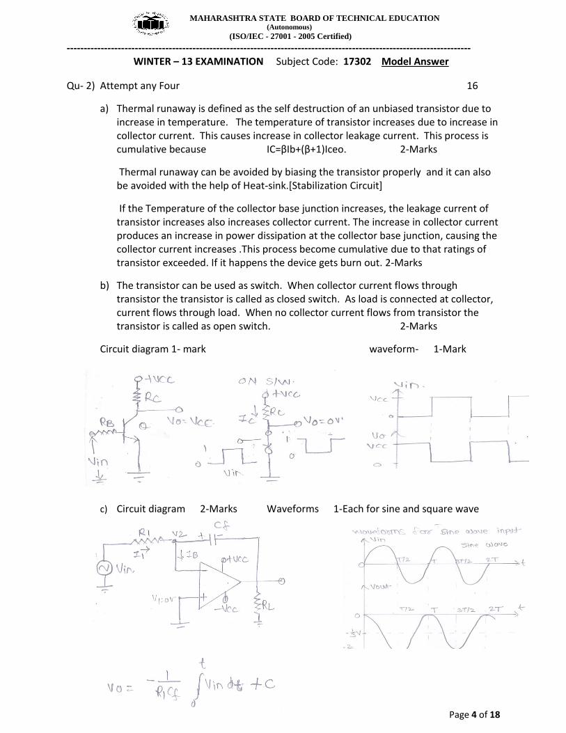
Qu- 2) Attempt any Four 16
a) Thermal runaway is defined as the self destruction of an unbiased transistor due to increase in temperature. The temperature of transistor increases due to increase in collector current. This causes increase in collector leakage current. This process is cumulative because IC=βIb+(β+1)Iceo. 2-Marks
Thermal runaway can be avoided by biasing the transistor properly and it can also be avoided with the help of Heat-sink.[Stabilization Circuit]
If the Temperature of the collector base junction increases, the leakage current of transistor increases also increases collector current. The increase in collector current produces an increase in power dissipation at the collector base junction, causing the collector current increases .This process become cumulative due to that ratings of transistor exceeded. If it happens the device gets burn out. 2-Marks
b) The transistor can be used as switch. When collector current flows through transistor the transistor is called as closed switch. As load is connected at collector, current flows through load. When no collector current flows from transistor the transistor is called as open switch. 2-Marks
Circuit diagram 1- mark waveform- 1-Mark
c) Circuit diagram 2-Marks Waveforms 1-Each for sine and square wave

MAHARASHTRA STATE BOARD OF TECHNICAL EDUCATION (Autonomous)
(ISO/IEC - 27001 - 2005 Certified)
----------------------------------------------------------------------------------------------------------------------- WINTER – 13 EXAMINATION Subject Code: 17302 Model Answer
Page 5 of 18
d) Circuit Diagram 2-Marks Waveform- 2 Marks
1.44 F= ------------------------ Hz
(RA+2RB) x C
e) Compare RC and LC oscillator 1 mark each point
parameters RC Oscillator LC oscillator
Voltage gain More Less
Oscillator frequency LOW HIGH
Components used Resistors and Capacitors Inductors and Capacitors
Applications Function generators Radio receivers, TV

MAHARASHTRA STATE BOARD OF TECHNICAL EDUCATION (Autonomous)
(ISO/IEC - 27001 - 2005 Certified)
----------------------------------------------------------------------------------------------------------------------- WINTER – 13 EXAMINATION Subject Code: 17302 Model Answer
Page 6 of 18
f) Full adder is the circuit which adds two binary bits along with carry generated from previous stage of adder. -1 Mark
Logic diagram 2 Marks
Truth Table of full adder 1-Mark
Cn-1 B A Sum Carry Out
0 0 0 0 0
0 0 1 1 0
0 1 0 1 0
0 1 1 0 1
1 0 0 1 0
1 0 1 0 1
1 1 0 0 1
1 1 1 1 1
Q. 3 a) Comparison of RC coupling and transformer coupling (1 mark for each point)
Point RC coupling Transformer coupling
Coupling element Resistor (R) & Capacitor (C) Transformer
Distortion Low Frequency distortion is present
Voltage gain Low High
Application AF amplifier, PA system, RF amplifier, Power Amp

MAHARASHTRA STATE BOARD OF TECHNICAL EDUCATION (Autonomous)
(ISO/IEC - 27001 - 2005 Certified)
----------------------------------------------------------------------------------------------------------------------- WINTER – 13 EXAMINATION Subject Code: 17302 Model Answer
Page 7 of 18
b) Logic symbol ( 1 mark each) Truth table (1 mark each)
2 input NAND gate
Logic symbol
Truth table
2 input EXOR logic gate
Logic symbol
Truth table
Input Output
A B Y
0 0 0
0 1 1
1 0 1
1 1 0
Input Output
A B Y
0 0 1
0 1 1
1 0 1
1 1 0

MAHARASHTRA STATE BOARD OF TECHNICAL EDUCATION (Autonomous)
(ISO/IEC - 27001 - 2005 Certified)
----------------------------------------------------------------------------------------------------------------------- WINTER – 13 EXAMINATION Subject Code: 17302 Model Answer
Page 8 of 18
C) JK flip flop[ using NAND gate (2 marks)
Race around condition : ( 2 marks)
- Race around condition occurs when all inputs of J-K flip flop are 1 ( J=K=CLK=1).
- J-K flip flop keep toggling indefinitely as long as J=K=CLK=1 and that condition is known as race around condition.
d) Logic circuit for 4:1 multiplexer (2marks)

MAHARASHTRA STATE BOARD OF TECHNICAL EDUCATION (Autonomous)
(ISO/IEC - 27001 - 2005 Certified)
----------------------------------------------------------------------------------------------------------------------- WINTER – 13 EXAMINATION Subject Code: 17302 Model Answer
Page 9 of 18
Truth Table ( 2 Marks)
Select Input Output
S1 S0 Y
0 0 d [0]
0 1 d [1]
1 0 d [2]
1 1 d [3]
e) Comparison of electrical & mechanical transducer (1 mark for each point)
Point Electrical Transducer Mechanical Transducer
Power supply requirement Required Not required
Reliability High Low
Life time More Less
Example LDR, PHOTODIODE, Solar cell
Mechanical flow meter, Bourdon tube, galvanometer
f) Functions robotics system: ( 2 marks)
- It is used to perform variety of task like moving material, parts, tools etc .
- It can also be used to perform a dedicated task through variable programming.
Applications robotics system ( any 2)
- Pick and place robots
- Mobile robot
- Industrial robot ( Manipulating)
- Android

MAHARASHTRA STATE BOARD OF TECHNICAL EDUCATION (Autonomous)
(ISO/IEC - 27001 - 2005 Certified)
----------------------------------------------------------------------------------------------------------------------- WINTER – 13 EXAMINATION Subject Code: 17302 Model Answer
Page 10 of 18
Q . 4) Attempt any four of the following
a) Advance vehicle condition system (AVCS): ( 1 mark for each point)
- AVCS technology combines various technologies like ABS, collision warning, automatic cruise control etc to provide full vehicle automation.
- It significantly enhances the transportation safety and capacity of highway.
- It also improves the driver behavior in risky situations by providing warnings, speed controls, intelligent cruise control etc.
- In AVCS driver is replaced by full automatic steering of vehicles which helps to reduce accident and increase traffic flow.
Advance vehicle control system
b) Circuit diagram of single stage transistor amplifier (2 marks)
Requirements ( ½ marks for each point)
1) Biasing resistors (R1,R2) are required to biased the transistor in active region
2) Input & output Coupling capacitor ( C1 & C2) are used to couple the AC signal to input terminal & to load respectively.
3) Emitter bypass Capacitor ( CE) used to bypass emitter resistor for AC condition.

MAHARASHTRA STATE BOARD OF TECHNICAL EDUCATION (Autonomous)
(ISO/IEC - 27001 - 2005 Certified)
----------------------------------------------------------------------------------------------------------------------- WINTER – 13 EXAMINATION Subject Code: 17302 Model Answer
Page 11 of 18
4) High value Emitter resister RE for high Q point stability under DC operating condition.
c) Block diagram of PLC (2 Marks)
Functions: (1/2 marks each)
1) Input Module: Input can be digital or analog depends on process required. This module converts input quantity into CPU compatible signal.
2) CPU: It performs the function of controlling all operation of PLC like execution of operating system, memory management, monitoring input and output. It contains microprocessor which can be programmed as per requirement.
3) Memory: It is the part of CPU which stores both the program and data from equipment connected to PLC. ROM is used to store operating system and Ram is used to store user’s data/program.
4) Output Module: Various output modules are connected to output device depending upon the process. It can be actuator which can be ON or OFF based on input situations. Example: motor, timer, solenoid etc.
d) Data Logger : (2 marks)
- It automatically records the readings of instruments that are located at different parts of plant.
- It measures the output of transducer and logs that reading automatically.

MAHARASHTRA STATE BOARD OF TECHNICAL EDUCATION (Autonomous)
(ISO/IEC - 27001 - 2005 Certified)
----------------------------------------------------------------------------------------------------------------------- WINTER – 13 EXAMINATION Subject Code: 17302 Model Answer
Page 12 of 18
- It also perform the various functions like scanning, signal conditioning, recording.
- It perform the recording more quickly & accurately.
Applications: ( any 4 applications, 1 mark each)
- Refrigeration and Freezer (including Food & Medical Storage and Transportation) - Agriculture, Horticulture, Environmental Studies - Server Room Monitoring - Industrial Processes
e) Block diagram of multichannel DAS (4 marks)
f) Comparison of PN junction diode and Zener diode ( 1 mark for each point)
Point PN junction diode Zener diode
Direction of conduction Forward Reverse
Application Rectifier Voltage regulator
Reverse breakdown Occur Does not occur
Symbol

MAHARASHTRA STATE BOARD OF TECHNICAL EDUCATION (Autonomous)
(ISO/IEC - 27001 - 2005 Certified)
----------------------------------------------------------------------------------------------------------------------- WINTER – 13 EXAMINATION Subject Code: 17302 Model Answer
Page 13 of 18
5 a. AC signal Conditioning: It is the process used in instrumentation and measurement
system to modify or improve output of the various transducers. Improvement of signal
is necessary so as to make them useful and compatible with the measuring system. It
consists of number of circuits or blocks.
Types of circuits used in AC signal Conditioning
a) Calibration and zeroing network (offset nullifying circuit)
b) AC amplifier
c) Phase detector
d) Low pass filter
e) Power supply
2
2
b. Selection Criteria for transducers: (Any eight points)
a) Nature and range of the physical parameter to be measured.
b) Type of the physical quantity.
c) Transducer should be compatible with measuring system.
d) Performance of the transducer should be linear.
e) Performance of the transducer should be stable under operating conditions.
f) Transducer should have high sensitivity
g) Transducer should have high accuracy
h) Transducer should have better repeatability.
i) It should have high input impedance and low output impedance to avoid the
loading effect.
j) Transducer should be free from drift, noise and offset problems.
k) Transducer should have flat frequency response.
l) Transducer should be easily available at low cost in the market with essential
accessories for its installation.
m) Transducer should be portable and light in weight.
n) Any other relevant and accurate criteria may be considered.
½ * 8

MAHARASHTRA STATE BOARD OF TECHNICAL EDUCATION (Autonomous)
(ISO/IEC - 27001 - 2005 Certified)
----------------------------------------------------------------------------------------------------------------------- WINTER – 13 EXAMINATION Subject Code: 17302 Model Answer
Page 14 of 18
Q.N
o
Model Answer/Solution Mark
s
5 c. Comparison of BJT and FET
Parameter BJT FET
Terminals It has three terminals Emitter,
Base and Collector
It has four terminals
Drain ,Gate, Source
and Substrate {Body}
Type’s Two types NPN and PNP Two Types JFET and
MOSFET and/or N-
channel and P-channel
Input impedance Input junction is forward biased
so input impedance is very
low.
Input junction is reverse
biased so input
impedance is very high.
Controlling factor Output current is controlled by
input current so current
controlled device
Output current is
controlled by input [gate]
voltage so Voltage
controlled device
01
01
01
01
d
.
Optocoupler: It is a combination of photo (light) source and photo sensor
(detector) in a same package. They are used to couple the signal from one point
to other point optically with electrical isolation.
Advantages: [minimum 4]
a) No electrical connection between input and output.
b) Optical section controls output signal and ultimately the load.
c) No effect of electromagnetic interference.
d) No possibility of feedback voltage
e) It provides more stability
f) High reliability
g) Output is TTL compatible
h) Large bandwidth
i) Good frequency response
02
½ * 4
e. Comparison of microprocessor and microcontroller
Parameter Microprocessor Microcontroller
Components It is a CPU It consists of CPU, RAM,
ROM, I/O ports, timer,
Converters
Access time High Less
Number of opcodes Less More
Hardware required RAM, ROM, I/O ports, timer,
converters externally.
In built
01
01
01
01

MAHARASHTRA STATE BOARD OF TECHNICAL EDUCATION (Autonomous)
(ISO/IEC - 27001 - 2005 Certified)
----------------------------------------------------------------------------------------------------------------------- WINTER – 13 EXAMINATION Subject Code: 17302 Model Answer
Page 15 of 18
Q.No Model Answer/Solution Marks
5 f. Doping:- A process of adding impurity to a pure semiconductor is known
as
Doping.
For forming p-type semiconductor trivalent impurity such as Gallium is
added. And
For forming n-type semiconductor pentavalent impurity such as is Arsenic
added.
02
01
01
6 Attempt any FOUR of the Following 16
a. Block diagram of regulated power supply
vin
ac
04 M
waveforms
are also
shown to
each
block
b. Load Regulation:-
It is the rate of change of output voltage with respect to
change in load resistance. It shows the change in output voltage with
change in value of load resistance or load current. It is always calculated
in percentage.
Line Regulation :- It is the rate of change of output voltage with respect to
change in input voltage{line voltage}. It shows the change in output
voltage with change in input ac voltage. It is also calculated in percentage.
02
02
c. Barkhausen’s Criteria :-
Barkhausen’s criterion is applicable for oscillators.
02
Step down
Transformer
Rectifier
RECTIFIER
FILTER
Voltage
Regulator
REGULATOR
DC
output

MAHARASHTRA STATE BOARD OF TECHNICAL EDUCATION (Autonomous)
(ISO/IEC - 27001 - 2005 Certified)
----------------------------------------------------------------------------------------------------------------------- WINTER – 13 EXAMINATION Subject Code: 17302 Model Answer
Page 16 of 18
According to this criteria the circuit has to satisfy two conditions
First:- the total phase shift given by the circuit should be 3600 or 0
0. And
Second :- The factor A should be less than equal to one.
Positive type feedback is used in osciilator’s.
Oscillators
Sinusoidal Non
sinusoidal
Low frequency High frequency
Wein bridge oscillator Hartley oscillator
RC phase shift oscillator Colpitts oscillator
Crystal oscillator
01
01
Q.No Model Answer/Solution Marks
6 d. Different triggering methods.
There are two types of triggering methods
I] Level trigger II] Edge trigger
Level triggering is of two types
A] positive level triggering B] Negative level triggering
clk Clk
clk
o/p clk o/p
o/p changes on logic’1’ level of clk o/p changes on logic’0’
level of clk
Edge trigger are also of two types
A] Positive edge trigger{Rising Edge} B] Negative edge
trigger{falling/tralling}
clk
clk o/p
o/p
o/p changes when clk goes from 0 to1 o/p changes when clk goes
from 1 to0
1/2 for
each
method
and
1/2 for
each
waveform
½*4=2M
for
methods
and
½*4=2M
for
waveforms
FF
FF
FF FF

MAHARASHTRA STATE BOARD OF TECHNICAL EDUCATION (Autonomous)
(ISO/IEC - 27001 - 2005 Certified)
----------------------------------------------------------------------------------------------------------------------- WINTER – 13 EXAMINATION Subject Code: 17302 Model Answer
Page 17 of 18
e. Selection factors for PLC
a) Type of PLC: Analog or Digital
b) Number of inputs and outputs to PLC
c) Operating voltage and operating current range
d) Scan time of PLC
e) Memory size of PLC
f) Type of memory of PLC
g) Type of programming
h) Reliability of PLC
i) Flexibility of PLC
j) Any other relevant and accurate point
½*8=4M
6 f. Decade Counter
For decade counter number of Flipflops required are 2N
>= count
So 24 > 10{decade} so for decade counter 4 flipflops are required but 4
flopflops will count total 16 clock pulses so 6 clock pulses are eliminated
by using external logic.
Synchronous Counter
LOGIC ‘1’
J0 Q0 J1 Q1 J2 Q2 J3 Q3
Clk K0 K1 K2 K3
cl cl cl cl
Q0 Q1 Q2 Q3
Input connection-
J0= K0=1 , J1= Q0 Q3
K1= Q0
J2 =K2= Q0Q1
J3= Q0Q1Q2
K3= Q0
02
Q0Q1Q2 Q0Q1 Q0
Q1 Q2

MAHARASHTRA STATE BOARD OF TECHNICAL EDUCATION (Autonomous)
(ISO/IEC - 27001 - 2005 Certified)
----------------------------------------------------------------------------------------------------------------------- WINTER – 13 EXAMINATION Subject Code: 17302 Model Answer
Page 18 of 18
OR
Asynchronous Counter
Logic’1’
T0 Q0 T1 Q1 T2 Q2 T3
Q3
Clk
Q0 Q1 Q2
Instead of active low clear control signal one may show active high
clear and AND gate is used.
Truth Table for decade counter
Clk Q3 Q2 Q1 Q0
0 0 0 0 0
1 0 0 0 1
2 0 0 1 0
3 0 0 1 1
4 0 1 0 0
5 0 1 0 1
6 0 1 1 0
7 0 1 1 1
8 1 0 0 0
9 1 0 0 1
02
Q3