MAHARASHTRA STATE BOARD OF TECHNICAL EDUCATION (Autonomous...
24
MAHARASHTRA STATE BOARD OF TECHNICAL EDUCATION (Autonomous) (ISO/IEC - 27001 - 2005 Certified) Page 1 of 24 Subject Title: Basic Electronics Subject Code: Important Instructions to examiners: 1) The answers should be examined by key words and not as word-to-word as given in the model answer scheme. 2) The model answer and the answer written by candidate may vary but the examiner may try to assess the understanding level of the candidate. 3) The language errors such as grammatical, spelling errors should not be given more Importance (Not applicable for subject English and Communication Skills. 4) While assessing figures, examiner may give credit for principal components indicated in the figure. The figures drawn by candidate and model answer may vary. The examiner may give credit for any equivalent figure drawn. 5) Credits may be given step wise for numerical problems. In some cases, the assumed constant values may vary and there may be some difference in the candidate’s answers and model answer. 6) In case of some questions credit may be given by judgement on part of examiner of relevant answer based on candidate’s understanding. 7) For programming language papers, credit may be given to any other program based on equivalent concept. 17321
Transcript of MAHARASHTRA STATE BOARD OF TECHNICAL EDUCATION (Autonomous...

MAHARASHTRA STATE BOARD OF TECHNICAL EDUCATION (Autonomous)
(ISO/IEC - 27001 - 2005 Certified)
Page 1 of 24
Subject Title: Basic Electronics Subject Code:
Important Instructions to examiners: 1) The answers should be examined by key words and not as word-to-word as given in the
model answer scheme. 2) The model answer and the answer written by candidate may vary but the examiner may
try to assess the understanding level of the candidate. 3) The language errors such as grammatical, spelling errors should not be given more
Importance (Not applicable for subject English and Communication Skills. 4) While assessing figures, examiner may give credit for principal components indicated in
the figure. The figures drawn by candidate and model answer may vary. The examiner may give credit for any equivalent figure drawn.
5) Credits may be given step wise for numerical problems. In some cases, the assumed constant values may vary and there may be some difference in the candidate’s answers and model answer.
6) In case of some questions credit may be given by judgement on part of examiner of relevant answer based on candidate’s understanding.
7) For programming language papers, credit may be given to any other program based on equivalent concept.
17321

MAHARASHTRA STATE BOARD OF TECHNICAL EDUCATION (Autonomous)
(ISO/IEC - 27001 - 2005 Certified)
Page 2 of 24
Q.1 Attempt any TEN from following 20 Marks
a) Define intrinsic and extrinsic semiconductor with examples
Ans: [Each definition for 1M]
Intrinsic Semiconductor: A semiconductor which is extremely pure form is known as Intrinsic
semiconductor
Example of intrinsic semiconductor are Germanium and silicon
Extrinsic Semiconductor :A semiconductor which is impure semiconductor in which a small amount of
suitable impurity added to increase its conductivity.
Example of extrinsic semiconductor are gallium, Indium, Boron, Arsenic and Phosphorous .
b) Draw the symbol of LED and photodiode.
Ans: [ Each symbol for 1M]
LED Photo diode
c) List the four specifications of zener diode.
Ans: [ For each specification ½ M]
1. Zener voltage (VZ)
2. Zener current (IZ)
3. Zener resistance (RZ)
4. Power rating
d) State the need of biasing of BJT.
Ans: [ Any relevant answer can be consider for 2M]
Need:
Thebasicneedoftransistorbiasingistokeepthebase-emitter(B-E)junctionproperly
forwardbiasedandthecollector-emitter(C-E)junctionproperly reversebiasedduringthe
application ofA.C. signal.
To fixed operating point at the center of load line.

MAHARASHTRA STATE BOARD OF TECHNICAL EDUCATION (Autonomous)
(ISO/IEC - 27001 - 2005 Certified)
Page 3 of 24
To ensure that operating point does not shift from its place during its process
Thistypeoftransistorbiasingisnecessary fornormalandproperoperationoftransistorto
beusedforamplificationor for getting faithful amplification.
e) Define gain and bandwidth of an amplifier.
Ans: [ Each definition for 1M]
Bandwidth
Therangeoffrequencyoverwhichthevoltagegainofanamplifierremainsconstantis known as
bandwidth of an amplifier.
OR
The range of frequency over which the voltage gain is equal to or greater than 70.7% of its
maximum value
Gain:
The ratio of output parameter (voltage/ current /power) to the input parameter (voltage/ current /power) of an amplifier is known as gain. It is denoted by a letter A
f) What is oscillator ? Give its classification.
Ans.[Oscillator explanation 1M , classification 1M]
Anoscillatorisaelectroniccircuitthatproducesaperiodicac waveformof desired frequency
withonly dcsupplyvoltageasan input i.e. without any ac input signal .
Classification of Oscillator :
1) RC oscillator 2) LC oscillator 3) Crystal Oscillator
g) Why BJT is called bipolar junction transistor.
Ans. [ 2M for correct answer]
Ans: BJT is called bipolar junction transistor because in BJT current conduction takes place due to majority
as well as minority charge carriers.
h) Give the different types of amplifier coupling .
Ans :[ 2m for all three types]
1. Resistance – capacitance(RC) coupling.
2. Transformer coupling
3. Direct coupling
i) Draw symbol of D-MOSFET. (n-channel and P-channel)

MAHARASHTRA STATE BOARD OF TECHNICAL EDUCATION (Autonomous)
(ISO/IEC - 27001 - 2005 Certified)
Page 4 of 24
Ans: [ Each symbol for 1M]
j) Write down output voltage for 7805 IC and IC 7912.
Ans:[ 1 M for each IC output voltage]
The output voltage of 7805 is +5 Volts and 7912 is -12 Volts
k) State Barkhausen’s Criterion for sustained oscillations.
Ans:[1M forone condition]
Barkhausen’sCriterionforOscillations
The necessary condition for sustained oscillations are
1.Product of voltage gain and feedback factor should be equal to and greater thanLoopgain (β.Av) ≥ 1
2. Phaseshift between theinput and output signal or around the loop must be equalto 360⁰or 0⁰.

MAHARASHTRA STATE BOARD OF TECHNICAL EDUCATION (Autonomous)
(ISO/IEC - 27001 - 2005 Certified)
Page 5 of 24
l) What do you mean by universal gate ? Give its type
Ans :[Brief explanation 1M, types/example 1M]
A universal gate is a gate which can implement any Boolean function or equation and any logic
gate without need to use any othergate type.
The NAND and NOR gates are universal gates.
m) Convert : (i) (2F9A) 16 = (?) 2
(ii)(110101) 2 = ( ?) 10
Ans: [ for each sum 2M]
n) Give the difference between RC and LC oscillator
Ans: [Any two points 2M]
Parameter RC Oscillator LC Oscillator
Type of oscillator according to frequency range
Low frequency Oscillator High frequency Oscillator
Components used in feedback network
Resistors and Capacitors used in feedback network
Inductors and Capacitors used in feedback network
Examples RC phase shift oscillator ,Wein bridge oscillator
Hartely Oscillator , Colpitts Oscillator
Q. 2: Attempt any four of the following 16 M
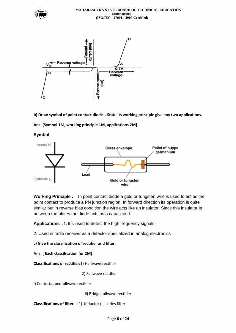
a) Draw and label VI characteristics of p-n junction diode in forward bias and reverse bias.
Ans: [ Forward characteristics 2M , Reverse characteristics 2M]
MAHARASHTRA STATE BOARD OF TECHNICAL EDUCATION (Autonomous)
(ISO/IEC - 27001 - 2005 Certified)
Page 6 of 24
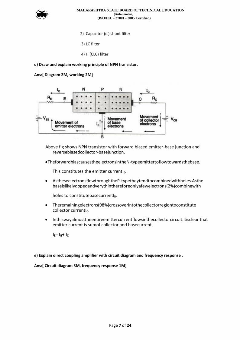
b) Draw symbol of point contact diode . State its working principle give any two applications.
Ans: [Symbol 1M, working principle 1M, applications 2M]
Symbol
Working Principle : In point contact diode a gold or tungsten wire is used to act as the
point contact to produce a PN junction region. In forward direction its operation is quite
similar but in reverse bias condition the wire acts like an insulator. Since this insulator is
between the plates the diode acts as a capacitor. I
Applications :1. It is used to detect the high frequency signals .
2. Used in radio receiver as a detector specialized in analog electronics
c) Give the classification of rectifier and filter.
Ans: [ Each classification for 2M]
Classifications of rectifier:1) Halfwave rectifier
2) Fullwave rectifier
i) Centertappedfullwave rectifier
ii) Bridge fullwave rectifier
Classifications of filter : 1) Inductor (L) series filter
MAHARASHTRA STATE BOARD OF TECHNICAL EDUCATION (Autonomous)
(ISO/IEC - 27001 - 2005 Certified)
Page 7 of 24
2) Capacitor (c ) shunt filter
3) LC filter
4) П (CLC) filter
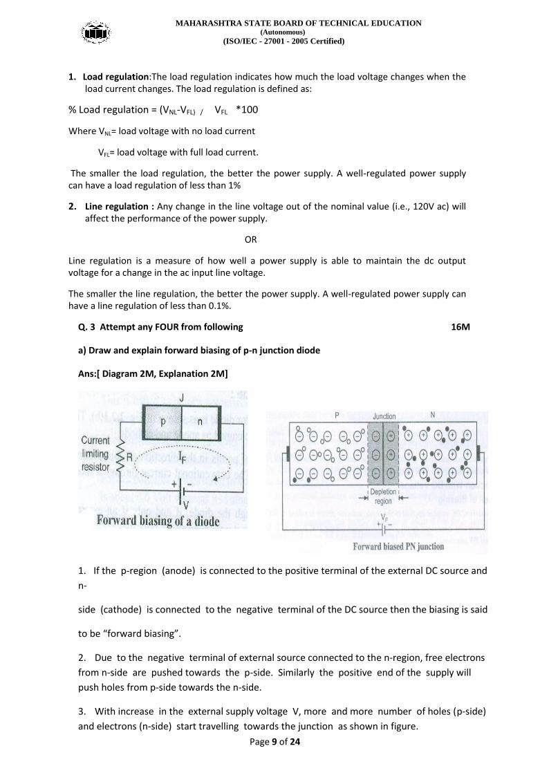
d) Draw and explain working principle of NPN transistor.
Ans:[ Diagram 2M, working 2M]
Above fig shows NPN transistor with forward biased emitter-base junction and reversebiasedcollector-basejunction.
TheforwardbiascausestheelectronsintheN-typeemittertoflowtowardsthebase.
This constitutes the emitter currentIE.
AstheseelectronsflowthroughtheP-typetheytendtocombinedwithholes.Asthe baseislikelydopedandverythinthereforeonlyafewelectrons(2%)combinewith
holes to constitutebasecurrentIB.
Theremainingelectrons(98%)crossoverintothecollectorregiontoconstitute collector currentIC.
Inthiswayalmosttheentireemittercurrentflowsinthecollectorcircuit.Itisclear that emitter current is sumof collector and basecurrent.
IE= IB+ IC
e) Explain direct coupling amplifier with circuit diagram and frequency response .
Ans:[ Circuit diagram 3M, frequency response 1M]

MAHARASHTRA STATE BOARD OF TECHNICAL EDUCATION (Autonomous)
(ISO/IEC - 27001 - 2005 Certified)
Page 8 of 24
OR
f) What is need of regulated power supply ? Define load regulation and line regulation .
Ans: [Need 2M,Each definition for 1 M]
Need ofregulated powersupply.
TheunregulatedD.C.powersupply suffersfromthedisadvantagesofpoorvoltageregulation and high ripplefactor.
Thismayresulttheerraticoperationofmostoftheelectronicdevicesandcircuitsandalso electronicgadgetssuchas pocketradios,electronic calculators,digitalwatches/clocks,tape recordersetc.
In order to avoid erratic operations of electronic circuits and also to improve voltage regulationand ripplefactor, thereisnecessityofregulated D.C. power supply.
MAHARASHTRA STATE BOARD OF TECHNICAL EDUCATION (Autonomous)
(ISO/IEC - 27001 - 2005 Certified)
Page 9 of 24
1. Load regulation:The load regulation indicates how much the load voltage changes when the load current changes. The load regulation is defined as:
% Load regulation = (VNL-VFL) / VFL *100
Where VNL= load voltage with no load current
VFL= load voltage with full load current.
The smaller the load regulation, the better the power supply. A well-regulated power supply can have a load regulation of less than 1%
2. Line regulation : Any change in the line voltage out of the nominal value (i.e., 120V ac) will affect the performance of the power supply.
OR
Line regulation is a measure of how well a power supply is able to maintain the dc output voltage for a change in the ac input line voltage.
The smaller the line regulation, the better the power supply. A well-regulated power supply can have a line regulation of less than 0.1%.
Q. 3 Attempt any FOUR from following 16M
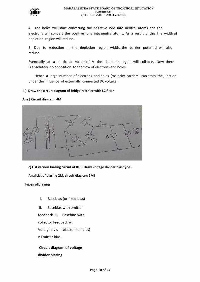
a) Draw and explain forward biasing of p-n junction diode
Ans:[ Diagram 2M, Explanation 2M]
1. If the p-region (anode) is connected to the positive terminal of the external DC source and
n-
side (cathode) is connected to the negative terminal of the DC source then the biasing is said
to be “forward biasing”.
2. Due to the negative terminal of external source connected to the n-region, free electrons
from n-side are pushed towards the p-side. Similarly the positive end of the supply will
push holes from p-side towards the n-side.
3. With increase in the external supply voltage V, more and more number of holes (p-side)
and electrons (n-side) start travelling towards the junction as shown in figure.
MAHARASHTRA STATE BOARD OF TECHNICAL EDUCATION (Autonomous)
(ISO/IEC - 27001 - 2005 Certified)
Page 10 of 24
4. The holes will start converting the negative ions into neutral atoms and the
electrons will convert the positive ions into neutral atoms. As a result of this, the width of
depletion region will reduce.
5. Due to reduction in the depletion region width, the barrier potential will also
reduce.
Eventually at a particular value of V the depletion region will collapse. Now there
is absolutely no opposition to the flow of electrons and holes.
Hence a large number of electrons and holes (majority carriers) can cross the junction
under the influence of externally connected DC voltage.
b) Draw the circuit diagram of bridge rectifier with LC filter
Ans:[ Circuit diagram 4M]
c) List various biasing circuit of BJT . Draw voltage divider bias type .
Ans:[List of biasing 2M, circuit diagram 2M]
Types ofbiasing
i. Basebias (or fixed bias)
ii. Basebias with emitter
feedback. iii. Basebias with
collector feedback iv.
Voltagedivider bias (or self bias)
v.Emitter bias.
Circuit diagram of voltage
divider biasing
MAHARASHTRA STATE BOARD OF TECHNICAL EDUCATION (Autonomous)
(ISO/IEC - 27001 - 2005 Certified)
Page 11 of 24
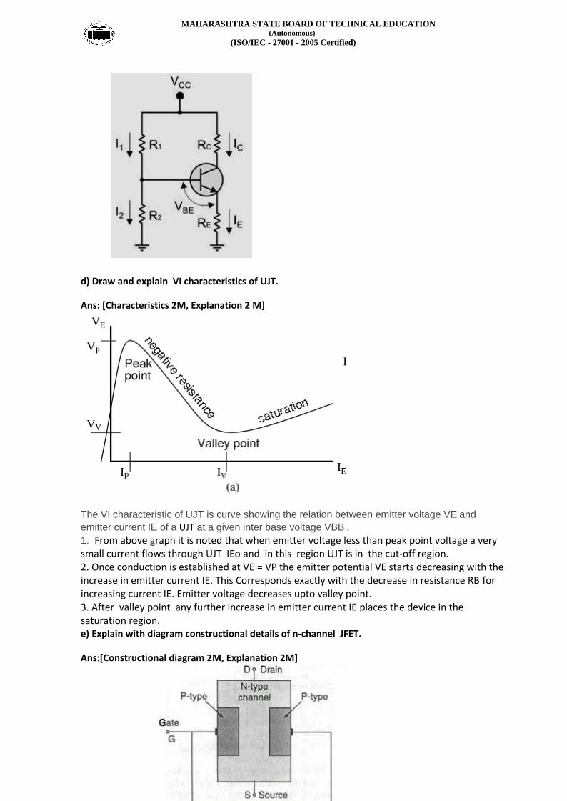
d) Draw and explain VI characteristics of UJT.
Ans: [Characteristics 2M, Explanation 2 M]
The VI characteristic of UJT is curve showing the relation between emitter voltage VE and
emitter current IE of a UJT at a given inter base voltage VBB .
1. From above graph it is noted that when emitter voltage less than peak point voltage a very small current flows through UJT IEo and in this region UJT is in the cut-off region. 2. Once conduction is established at VE = VP the emitter potential VE starts decreasing with the increase in emitter current IE. This Corresponds exactly with the decrease in resistance RB for increasing current IE. Emitter voltage decreases upto valley point. 3. After valley point any further increase in emitter current IE places the device in the saturation region. e) Explain with diagram constructional details of n-channel JFET.
Ans:[Constructional diagram 2M, Explanation 2M]

MAHARASHTRA STATE BOARD OF TECHNICAL EDUCATION (Autonomous)
(ISO/IEC - 27001 - 2005 Certified)
Page 12 of 24
N-channel JFET consist of an N-type semiconductor bar with two P-type heavily doped regions
diffused on opposite sides of its middle part . The P-type region forms two PN junctions . The space
between these two junctions is called channel . Both P-type regions are internally connected an and
single terminal is taken out is called Gate. Two terminals from opposite ends of N-type channel
called drain and source. The drain is the terminal through which electrons leave the bar and source
is the terminal through electron enter the bar .
f) Give symbol and truth table of AND and OR gate .
Ans: [2M for each gate]
Q.4 Attempt any FOUR of the following 16M
a) Compare halfwave ,centre tap and bridge type fullwave rectifier on the basis of (i) Ripple factor (ii)
Rectification efficiency (iii) TUF and (iv) PIV
Ans .[Anyfourpoints:4 M]
Sr.No Parameters HalfWave Centre tap Bridge Full
Wave I Ripple Factor 1.21 0.482 0.482
ii Rectification efficiency
efficiency, ηmax
40.6% 81.2% 81.2%
iii Transformer utilization
factor(TUF)
0.324 0.671 0.813
iv Peak inverse
voltage(PIV)
Vm 2Vm Vm

MAHARASHTRA STATE BOARD OF TECHNICAL EDUCATION (Autonomous)
(ISO/IEC - 27001 - 2005 Certified)
Page 13 of 24
b) Draw output characteristics of CE configuration and show various regions of BJT.
Ans: [ Neat and labelled characteristics 4M]
c) Draw two stage RC coupled amplifier and draw its frequency response .
Ans:

MAHARASHTRA STATE BOARD OF TECHNICAL EDUCATION (Autonomous)
(ISO/IEC - 27001 - 2005 Certified)
Page 14 of 24
Frequency response of RC coupled two stage amplifier
d) Explain working principle of N-channel depletion type MOSFET with construction diagram.
Ans:[ Diagram: 2M;Explanation: 2M]
Basic Operation
ThisMOSFETcanbeoperatedintwodifferentmodes,namely,DepletionModeandEnhancement Mode.
In depletion Mode, MOSFET is with negativegateto sourcevoltage. The negativevoltageon thegate induces a positivechargein the channel.Dueto this, free electrons in thevicinityof positive chargeare repelled awayin the channel.Thus, the channel is depleted of free electrons,reducingthenumber of freeelectrons that are passingthrough thechannel. Thus, negativegateto sourcevoltageis increased and the value ofdrain voltageVGSis totallydepleted offree electronsand hencedrain current reduces to zero.
In Enhancement mode, apositivegate to sourcevoltageis applied.Thepositivegate voltageincreases the numberof freeelectrons passingthrough the channel. Thegreaterthe gate voltage,greater is the number offreeelectrons passingthrough thechannel. This enhances the conducting ofthe channel.
e) Explain how zener diode can be used as voltage regulator.
Ans:[ Circuit diagram 2M, Explanation 2M]
MAHARASHTRA STATE BOARD OF TECHNICAL EDUCATION (Autonomous)
(ISO/IEC - 27001 - 2005 Certified)
Page 15 of 24
Working
For proper operation, the input voltage Vi must be greater than the Zener voltage Vz. This ensures that the Zener diode operates in the reverse breakdown condition. The unregulated input voltage Vi is applied to the Zener diode.
Suppose this input voltage exceeds the Zener voltage. This voltage operates the Zener diode in reverse breakdown region and maintains a constant voltage, i.e. Vz = Vo across the load inspite of input AC voltage fluctuations or load current variations. The input current is given by, IS = Vi – Vz / Rs = Vi – Vo / Rs
We know that the input current IS is the sum of Zener current Iz and load current IL.
Therefore, IS= Iz + IL
orIz = Is - IL
As the load current increase, the Zener current decreases so that the input current remains
constant.According toKirchhoff‟s voltage law, theoutput voltage is givenby,
Vo= Vi– Is. Rs
As the input current is constant, the output voltage remains constant (i.e. unaltered or unchanged). The reverse would be true, if the load current decreases. This circuit is also correct for the changes in input voltage.
As the input voltage increases, more Zener current will flow through the Zener diode. This increases the input voltage Is, and also the voltage drop across the resistor Rs, but the load voltage Vo would remain constant. The reverse would be true, if the decrease in input voltage is not below Zener voltage
Thus, a Zener diode acts as a voltage regulator and the fixed voltage is maintained across the load resistor RL.
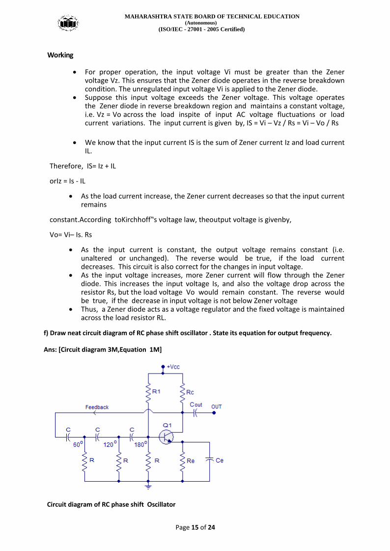
f) Draw neat circuit diagram of RC phase shift oscillator . State its equation for output frequency.
Ans: [Circuit diagram 3M,Equation 1M]
Circuit diagram of RC phase shift Oscillator
MAHARASHTRA STATE BOARD OF TECHNICAL EDUCATION (Autonomous)
(ISO/IEC - 27001 - 2005 Certified)
Page 16 of 24
Equation of output frequency =
√
Q .5 Attempt any FOUR of the following . 16M
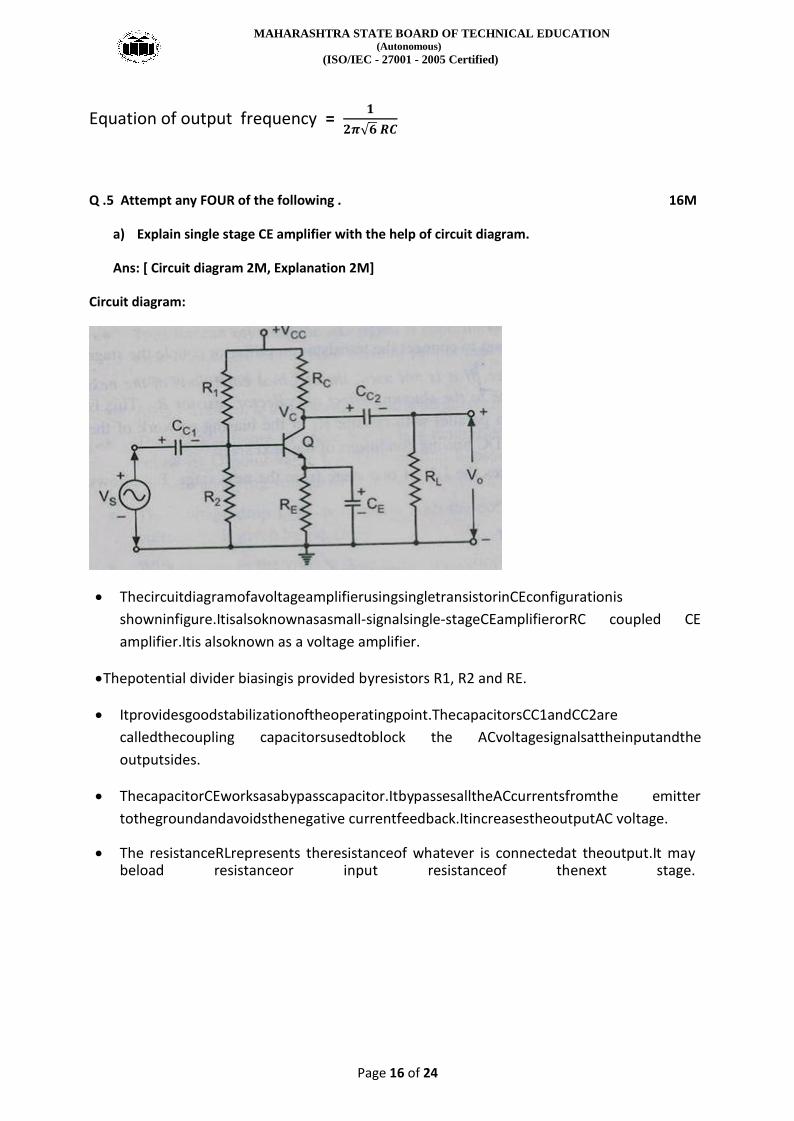
a) Explain single stage CE amplifier with the help of circuit diagram.
Ans: [ Circuit diagram 2M, Explanation 2M]
Circuit diagram:
ThecircuitdiagramofavoltageamplifierusingsingletransistorinCEconfigurationis
showninfigure.Itisalsoknownasasmall-signalsingle-stageCEamplifierorRC coupled CE
amplifier.Itis alsoknown as a voltage amplifier.
Thepotential divider biasingis provided byresistors R1, R2 and RE.
Itprovidesgoodstabilizationoftheoperatingpoint.ThecapacitorsCC1andCC2are
calledthecoupling capacitorsusedtoblock the ACvoltagesignalsattheinputandthe
outputsides.
ThecapacitorCEworksasabypasscapacitor.ItbypassesalltheACcurrentsfromthe emitter
tothegroundandavoidsthenegative currentfeedback.ItincreasestheoutputAC voltage.
The resistanceRLrepresents theresistanceof whatever is connectedat theoutput.It may beload resistanceor input resistanceof thenext stage.
MAHARASHTRA STATE BOARD OF TECHNICAL EDUCATION (Autonomous)
(ISO/IEC - 27001 - 2005 Certified)
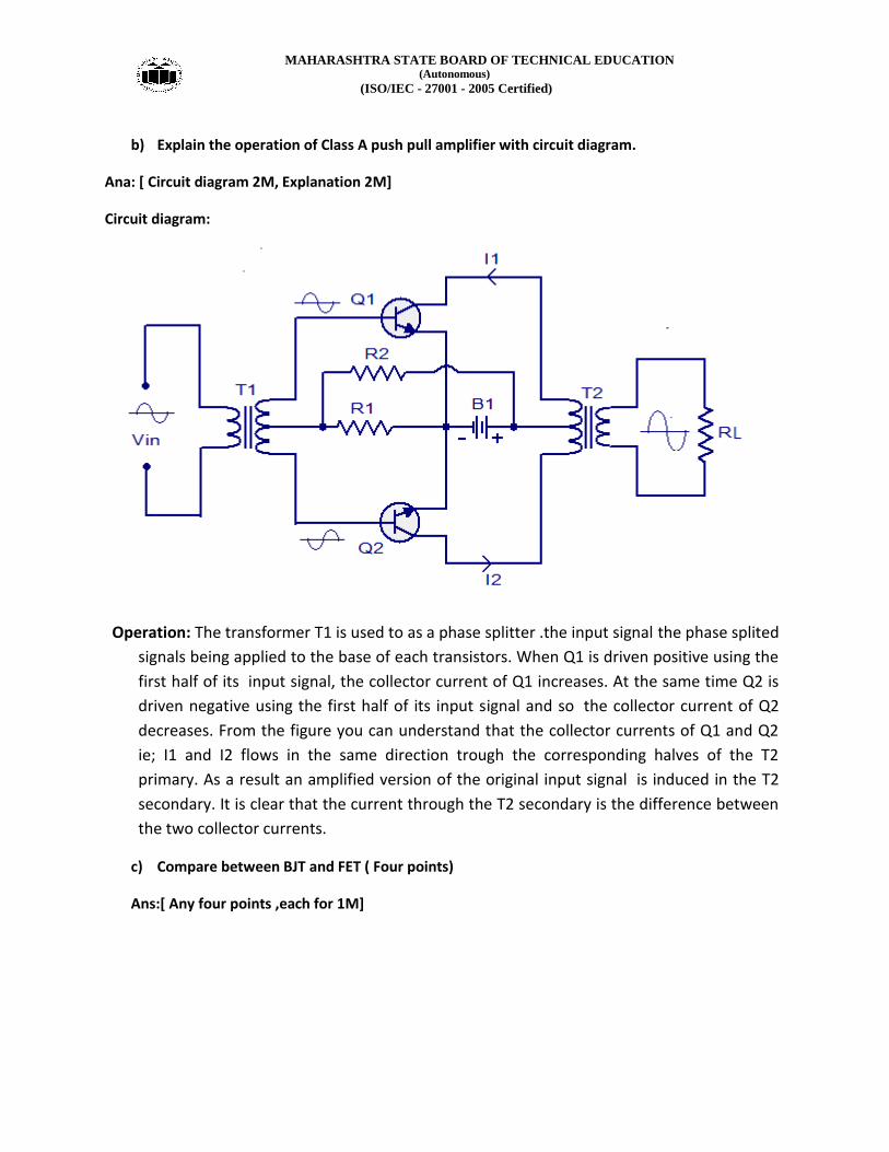
b) Explain the operation of Class A push pull amplifier with circuit diagram.
Ana: [ Circuit diagram 2M, Explanation 2M]
Circuit diagram:
Operation: The transformer T1 is used to as a phase splitter .the input signal the phase splited
signals being applied to the base of each transistors. When Q1 is driven positive using the
first half of its input signal, the collector current of Q1 increases. At the same time Q2 is
driven negative using the first half of its input signal and so the collector current of Q2
decreases. From the figure you can understand that the collector currents of Q1 and Q2
ie; I1 and I2 flows in the same direction trough the corresponding halves of the T2
primary. As a result an amplified version of the original input signal is induced in the T2
secondary. It is clear that the current through the T2 secondary is the difference between
the two collector currents.
c) Compare between BJT and FET ( Four points)
Ans:[ Any four points ,each for 1M]

MAHARASHTRA STATE BOARD OF TECHNICAL EDUCATION (Autonomous)
(ISO/IEC - 27001 - 2005 Certified)
Sr. no. BJT JFET
1. It is bipolardevicei.e.current in the
deviceis carried byelectrons and
holes.
It is unipolardevicei.e.current in the
deviceis carried byeither electrons
orholes. 2. It is current controlled devicei.e.
base current controls
thecollector current.
It is voltagecontrolled devicei.e.
voltageat thegate terminal controls
the amountof current flowing
through the device. 3. Input resistanceis low, of theorder
ofseveral KΩ
Input resistanceis veryhigh, ofthe
order ofseveral MΩ 4. It has positive temperature
coefficient ofresistanceat high
current levels i.e. currentincreases as
the temperatureincreases.
It has negativetemperature
coefficient ofresistanceat high
current levels i.e.
currentdecreases as the
temperatureincreases.
5. It suffersfrom minoritycarrier It does not sufferfrom minority
d.Draw the block diagram of Dc regulated power supply and explain the function of each block.
Ans: [Block diagram 2 M, Function of each block 2 M]
Block diagram of regulated power supply:
1) Tranformer : It is used to convert ac voltage either ac high value or ac low value as per
requirement
2) Rectifier : R ectifier converts the transformer secondary a.c. voltage into pulsating voltage .

MAHARASHTRA STATE BOARD OF TECHNICAL EDUCATION (Autonomous)
(ISO/IEC - 27001 - 2005 Certified)
3) Filter :The pulsating d.c. voltage is applied to the filter it reduces the pulsations in the rectifier
d.c. output voltage . Basically filter is used to remove ac components which are present in the
rectifier output.
4) Voltage regulator : Finally, the voltage regulator performs two functions. Firstly, it reduces the
variations in the filtered output voltage. Secondly, it keeps the output voltage (Vout) nearly
constant whether the load current changes or there is change in input a.c. voltage.
e) Draw circuit diagram of Hartley oscillator give its two applications.
Ans: [ Circuit diagram 2M, Any 2 applications 2M]
Circuit diagram:
Applications
The Hartley oscillator is to produce a sine wave with the desired frequency Hartley oscillators are mainly used as radio receivers TV transmitter. The Hartley oscillator is Suitable for oscillations for providing carrier frequency to modulator
. f) Draw block diagram of microprocessor and state the function of each block.
Ans:[ Block diagram 2M, Function of blocks 2M]
Any relevant block diagram can be consider.

MAHARASHTRA STATE BOARD OF TECHNICAL EDUCATION (Autonomous)
(ISO/IEC - 27001 - 2005 Certified)
Registers:The 8085includes six registers, one accumulator, and one flag register, as shown in Figure. In
addition, it has two 16-bit registers: the stack pointer and the program counter. The 8085 has six
general-purpose registers to store 8-bit data; these are identified as B, C, D, E, H, and L.
Program Counter (PC): This 16-bit register deals with sequencing the execution of instructions. This
register is a memory pointer. The microprocessor uses this register to sequence the execution of the
instructions. The function of the program counter is to point to the memory address from which the
next byte is to be fetched. When a byte is being fetched, the program counter is automatically
incremented by one to point to the next memory location.
Stack Pointer (SP): The stack pointer is also a 16-bit register, used as a memory pointer. It points to a
memory location in R/W memory, called stack. The beginning of the stack is defined by loading 16-bit
address in the stack pointer.
Arithmetic & Logic Unit (ALU) :It performs various arithmetic and logic operations. The data is available
in accumulator and temporary/general purpose registers.
Arithmetic Operations: Addition, Subtraction, Increment, Decrement etc.
MAHARASHTRA STATE BOARD OF TECHNICAL EDUCATION (Autonomous)
(ISO/IEC - 27001 - 2005 Certified)
Logic Operations: AND, OR, X-OR, Complement etc.
Q.6 Attempt any FOUR of the following 16M
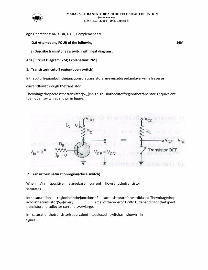
a) Describe transistor as a switch with neat diagram .
Ans.[Circuit Diagram: 2M; Explanation: 2M]
1. Transistorincutoff region(open switch)
Inthecutoffregionboththejunctionsofatransistorarereversebiasedandaverysmallreverse
currentflowsthrough thetransistor.
Thevoltagedropacrossthetransistor(VCE)ishigh.Thusinthecutoffregionthetransistoris equivalent toan open switch as shown in figure.
2. Transistorin saturationregion(close switch)
When Vin ispositive, alargebase current flowsandthetransistor
saturates.
Inthesaturation regionboththejunctionsof atransistorareforwardbiased.Thevoltagedrop acrossthetransistor(VCE)isvery smalloftheorderof0.2Vto1Vdependingonthetypeof transistorand collector current isverylarge.
In saturationthetransistorisequivalent toaclosed switchas shown in
figure.

MAHARASHTRA STATE BOARD OF TECHNICAL EDUCATION (Autonomous)
(ISO/IEC - 27001 - 2005 Certified)
b) Define α&β and derive the relation between α&β w. r. t. BJT.
Ans :[Each definition 1M, Derivation 2M]
α :The ratio of output collector current IC to input emitter current IE in theCB
configuration is called current gain alpha (α).
β:The ratio of output collector current IC to the input base current IB in theCE
configuration is called current gain beta (β) .
Relationship between α and β:
Weknow, IE=IB+IC
Dividingthe above equation on both sides
by IC, IE/IC=IB/IC+1
SinceIC/IE=α andIB/IC=β
So,IE/IC=1/ α andIC/IB=1/β
Therefore, 1/ α =(1/β) +1
hence1/ α = (1+β )/β
MAHARASHTRA STATE BOARD OF TECHNICAL EDUCATION (Autonomous)
(ISO/IEC - 27001 - 2005 Certified)
Therefore, α = β/(1+β)
c) Classify different types of power amplifier w.r.t. period of conduction of input signal.
Ans: [ for each type 1M]
Power amplifier are classified w.r.t period of conduction of input signal as:
1) Class A :In class A power amplifier transistor biased in a such way that output current
(Ic) flows for full cycle (360 °)of input signal .
2) Class B :In class Bpower amplifier transistor biased in a such way that output current (Ic)
flows for half cycle (180 °)of input signal .
3) Class C :In class C power amplifier transistor biased in a such way that output current
(Ic) flows for less than half cycle (<180 °)of input signal .
4) Class AB : In class AB power amplifier transistor biased in a such way that output
current (Ic) flows for more than half cycle and less than full cycle of input signal .(180
°< ᶲ <360 °) where ᶲ = conduction angle
d) Define : (i) Drain resistance
(ii) Mutual capacitance
(iii) Amplification factor
(iv) Pinch of voltage of FET
Ans: [Each definition 1M]
i) Drain resistance :It is ratio of change in drain to source voltage(∆VDS) to the corresponding
change in drain current (∆ID) for constant gate to source voltageVGS .
ii) Transconductance/ mutual conductance :It is ratio of change in Drain current (∆ID) to
change in Gate toSource Voltage (∆VGS) at a constant VDS.
iii) Amplification Factor : It isratioofchangeinDraintoSourceVoltage(∆VDS)to changeinGateto
SourceVoltage (∆VGS)ata constantID.
iv) Pinch off voltage :It is minimum value of drain to source voltage at which drain
current becomes constant
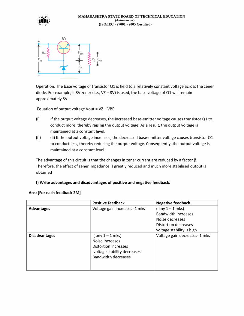
e) Draw transistorized series voltage regulator and explain its working .
Ans: [Circuit diagram 2M, working 2M]
MAHARASHTRA STATE BOARD OF TECHNICAL EDUCATION (Autonomous)
(ISO/IEC - 27001 - 2005 Certified)
Operation. The base voltage of transistor Q1 is held to a relatively constant voltage across the zener
diode. For example, if 8V zener (i.e., VZ = 8V) is used, the base voltage of Q1 will remain
approximately 8V.
Equation of output voltage Vout = VZ − VBE
(i) If the output voltage decreases, the increased base-emitter voltage causes transistor Q1 to
conduct more, thereby raising the output voltage. As a result, the output voltage is
maintained at a constant level.
(ii) (ii) If the output voltage increases, the decreased base-emitter voltage causes transistor Q1
to conduct less, thereby reducing the output voltage. Consequently, the output voltage is
maintained at a constant level.
The advantage of this circuit is that the changes in zener current are reduced by a factor β.
Therefore, the effect of zener impedance is greatly reduced and much more stabilised output is
obtained
f) Write advantages and disadvantages of positive and negative feedback.
Ans: [For each feedback 2M]
Positive feedback Negative feedback
Advantages Voltage gain increases -1 mks
( any 1 – 1 mks) Bandwidth increases Noise decreases Distortion decreases voltage stability is high
Disadvantages ( any 1 – 1 mks) Noise increases Distortion increases voltage stability decreases Bandwidth decreases
Voltage gain decreases- 1 mks