M54455EVB User's Manual - NXP
38
Freescale Semiconductor User’s Manual M54455EVBUM Rev. 4, 01/2008 Contents © Freescale Semiconductor, Inc., 2008. All rights reserved. 1 Introduction 1.1 Purpose This document provides design and usage information for the Freescale M54455EVB evaluation, development and reference platform. The M54455EVB platform provides an evaluation system for the Freescale MCF5445x ColdFire ® V4m embedded microprocessor family. The MCF54455 is the superset device in the family and is the processor featured on this platform. This allows evaluation and development for the entire family on a single hardware platform. 1.2 Related Documents • MCF54455 Reference Manual • M54455EVB Quick Start Guide • M54455EVB Schematics • MC34702 Switch-Mode with Linear Power Supply Datasheet 1 Introduction . . . . . . . . . . . . . . . . . . . . . . . . . . . . . . . . . . . 1 2 Overview . . . . . . . . . . . . . . . . . . . . . . . . . . . . . . . . . . . . . 2 2.1 MCF54455 Overview. . . . . . . . . . . . . . . . . . . . . . . . 2 2.2 M54455EVB Overview . . . . . . . . . . . . . . . . . . . . . . 4 2.3 Memory Map Overview . . . . . . . . . . . . . . . . . . . . . . 6 2.4 I/O Back Panel . . . . . . . . . . . . . . . . . . . . . . . . . . . . 7 3 Installation and Configuration . . . . . . . . . . . . . . . . . . . . . 7 4 Hardware Submodules . . . . . . . . . . . . . . . . . . . . . . . . . . 8 4.1 DDR SDRAM Interface . . . . . . . . . . . . . . . . . . . . . . 9 4.2 Reset Controller. . . . . . . . . . . . . . . . . . . . . . . . . . . . 9 4.3 MCF5445x Boot Options . . . . . . . . . . . . . . . . . . . . . 9 4.4 System Clocks. . . . . . . . . . . . . . . . . . . . . . . . . . . . 12 4.5 SPI Flash . . . . . . . . . . . . . . . . . . . . . . . . . . . . . . . . 14 4.6 Flash . . . . . . . . . . . . . . . . . . . . . . . . . . . . . . . . . . . 14 4.7 PCI . . . . . . . . . . . . . . . . . . . . . . . . . . . . . . . . . . . . 15 4.8 Audio . . . . . . . . . . . . . . . . . . . . . . . . . . . . . . . . . . . 19 4.9 BDM and JTAG . . . . . . . . . . . . . . . . . . . . . . . . . . . 20 4.10 USB . . . . . . . . . . . . . . . . . . . . . . . . . . . . . . . . . . . . 21 4.11 Ethernet . . . . . . . . . . . . . . . . . . . . . . . . . . . . . . . . . 21 4.12 ATA . . . . . . . . . . . . . . . . . . . . . . . . . . . . . . . . . . . . 22 4.13 FPGA. . . . . . . . . . . . . . . . . . . . . . . . . . . . . . . . . . . 22 4.14 CPLD . . . . . . . . . . . . . . . . . . . . . . . . . . . . . . . . . . . 26 4.15 Interrupts . . . . . . . . . . . . . . . . . . . . . . . . . . . . . . . . 33 4.16 Serial Interface Header . . . . . . . . . . . . . . . . . . . . . 33 4.17 Serial Ports . . . . . . . . . . . . . . . . . . . . . . . . . . . . . . 34 4.18 Logic Analyzer Connections . . . . . . . . . . . . . . . . . 35 4.19 Power Regulation . . . . . . . . . . . . . . . . . . . . . . . . . 35 4.20 Jumpers, Headers, and Switches . . . . . . . . . . . . . 35 5 U-Boot . . . . . . . . . . . . . . . . . . . . . . . . . . . . . . . . . . . . . . 37 6 Revision History. . . . . . . . . . . . . . . . . . . . . . . . . . . . . . . 37 M54455EVB User’s Manual by: Microcontroller Solutions Group
Transcript of M54455EVB User's Manual - NXP

Freescale SemiconductorUser’s Manual
M54455EVBUMRev. 4, 01/2008
Contents
Introduction . . . . . . . . . . . . . . . . . . . . . . . . . . . . . . . . . . . 1Overview . . . . . . . . . . . . . . . . . . . . . . . . . . . . . . . . . . . . . 2
2.1 MCF54455 Overview. . . . . . . . . . . . . . . . . . . . . . . . 22.2 M54455EVB Overview . . . . . . . . . . . . . . . . . . . . . . 42.3 Memory Map Overview . . . . . . . . . . . . . . . . . . . . . . 62.4 I/O Back Panel . . . . . . . . . . . . . . . . . . . . . . . . . . . . 7Installation and Configuration . . . . . . . . . . . . . . . . . . . . . 7Hardware Submodules . . . . . . . . . . . . . . . . . . . . . . . . . . 8
4.1 DDR SDRAM Interface . . . . . . . . . . . . . . . . . . . . . . 94.2 Reset Controller. . . . . . . . . . . . . . . . . . . . . . . . . . . . 94.3 MCF5445x Boot Options . . . . . . . . . . . . . . . . . . . . . 94.4 System Clocks. . . . . . . . . . . . . . . . . . . . . . . . . . . . 124.5 SPI Flash. . . . . . . . . . . . . . . . . . . . . . . . . . . . . . . . 144.6 Flash . . . . . . . . . . . . . . . . . . . . . . . . . . . . . . . . . . . 144.7 PCI . . . . . . . . . . . . . . . . . . . . . . . . . . . . . . . . . . . . 154.8 Audio . . . . . . . . . . . . . . . . . . . . . . . . . . . . . . . . . . . 194.9 BDM and JTAG . . . . . . . . . . . . . . . . . . . . . . . . . . . 204.10 USB . . . . . . . . . . . . . . . . . . . . . . . . . . . . . . . . . . . . 214.11 Ethernet . . . . . . . . . . . . . . . . . . . . . . . . . . . . . . . . . 214.12 ATA . . . . . . . . . . . . . . . . . . . . . . . . . . . . . . . . . . . . 224.13 FPGA. . . . . . . . . . . . . . . . . . . . . . . . . . . . . . . . . . . 224.14 CPLD. . . . . . . . . . . . . . . . . . . . . . . . . . . . . . . . . . . 264.15 Interrupts . . . . . . . . . . . . . . . . . . . . . . . . . . . . . . . . 334.16 Serial Interface Header . . . . . . . . . . . . . . . . . . . . . 334.17 Serial Ports . . . . . . . . . . . . . . . . . . . . . . . . . . . . . . 344.18 Logic Analyzer Connections . . . . . . . . . . . . . . . . . 354.19 Power Regulation . . . . . . . . . . . . . . . . . . . . . . . . . 354.20 Jumpers, Headers, and Switches . . . . . . . . . . . . . 35U-Boot . . . . . . . . . . . . . . . . . . . . . . . . . . . . . . . . . . . . . . 37Revision History. . . . . . . . . . . . . . . . . . . . . . . . . . . . . . . 37
M54455EVB User’s Manualby: Microcontroller Solutions Group
1 Introduction
1.1 PurposeThis document provides design and usage information for the Freescale M54455EVB evaluation, development and reference platform.
The M54455EVB platform provides an evaluation system for the Freescale MCF5445x ColdFire® V4m embedded microprocessor family. The MCF54455 is the superset device in the family and is the processor featured on this platform. This allows evaluation and development for the entire family on a single hardware platform.
1.2 Related Documents• MCF54455 Reference Manual• M54455EVB Quick Start Guide• M54455EVB Schematics• MC34702 Switch-Mode with Linear Power
Supply Datasheet
12
34
56
© Freescale Semiconductor, Inc., 2008. All rights reserved.

• Universal Serial Bus Specification, Revision 2.0• PCI Local Bus Specification, Revision 2.2• DDR2 SDRAM Specification (JESD79-2C)
2 Overview
2.1 MCF54455 OverviewThe MCF54455 is the host processor for the M54455EVB. Figure 1 shows a top-level block diagram of the MCF54455 superset device. The following is a brief summary of the functional blocks in the MCF54455 superset device.
• Version 4 ColdFire Core with MMU and EMAC— Up to 410 Dhrystone 2.1 MIPS @ 266 MHz
• 16 KBytes instruction cache and 16 KBytes data cache• 32 Kbytes internal SRAM• Support for booting from SPI-compatible flash, EEPROM, and FRAM devices• Crossbar switch technology (XBS) for concurrent access to peripherals or RAM from multiple bus
masters• 16 channel DMA controller• 16-bit 133MHz DDR/mobile-DDR/DDR2 Controller• USB 2.0 On-the-Go controller with ULPI support• 32-bit PCI controller @ 66MHz• ATA/ATAPI controller• Two 10/100 Fast Ethernet Controllers (FECn)• Cryptographic acceleration unit (CAU)• Random number generator• Synchronous serial interface• Four periodic interrupt timers• Four 32-bit timers with DMA support• DMA-supported serial peripheral interface (DSPI)• Three UARTs• I2C bus interface
M54455EVB User’s Manual, Rev. 4
2 Freescale Semiconductor
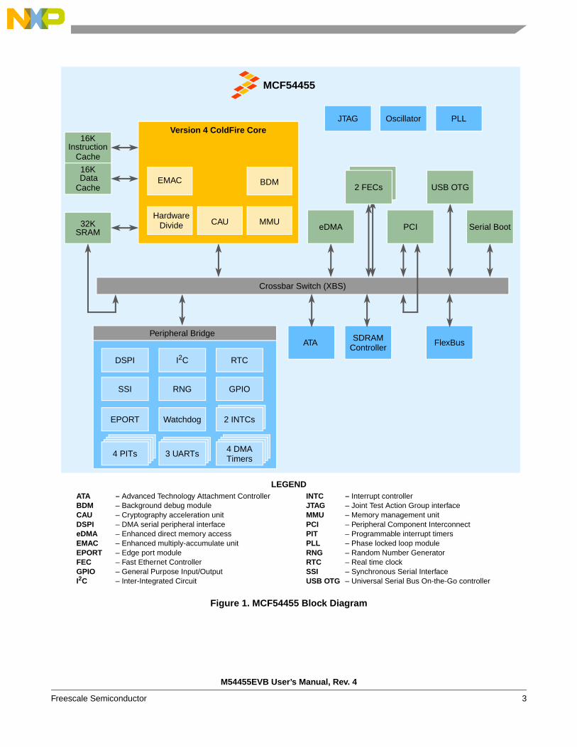
Figure 1. MCF54455 Block Diagram
Version 4 ColdFire Core
LEGEND
2 INTCs
DSPI
EPORT
3 UARTs
I2C
Watchdog
4 DMA
RTC
ATA – Advanced Technology Attachment ControllerBDM – Background debug moduleCAU – Cryptography acceleration unitDSPI – DMA serial peripheral interfaceeDMA – Enhanced direct memory accessEMAC – Enhanced multiply-accumulate unitEPORT – Edge port moduleFEC – Fast Ethernet ControllerGPIO – General Purpose Input/OutputI2C – Inter-Integrated Circuit
INTC – Interrupt controllerJTAG – Joint Test Action Group interfaceMMU – Memory management unitPCI – Peripheral Component InterconnectPIT – Programmable interrupt timersPLL – Phase locked loop moduleRNG – Random Number GeneratorRTC – Real time clockSSI – Synchronous Serial InterfaceUSB OTG – Universal Serial Bus On-the-Go controller
MCF54455
EMAC2 FECs
Crossbar Switch (XBS)
32KSRAM
Peripheral Bridge
CAU
16KInstruction
Cache
16KData
Cache
Timers
BDM
ATA SDRAMController
FlexBus
eDMA
USB OTG
4 PITs
SSI RNG GPIO
MMUHardware
Divide
Oscillator PLLJTAG
PCI Serial Boot
M54455EVB User’s Manual, Rev. 4
Freescale Semiconductor 3

2.2 M54455EVB OverviewThe M54455EVB provides hardware to evaluate as many of the configurations of the MCF5445x family as possible. The M54455EVB features:
• Freescale MCF54455 ColdFire microprocessor• DDR2 SDRAM (256 MByte)• Two NOR flash memory devices (16 MByte, 512 KByte)• Serial flash• MRAM (512 KByte, accessible through FPGA Flexbus interface)• Four PCI slots (32-bit, for MCF5445x as a PCI host system)• Two-port Ethernet interface• 40-pin ATA connector• Audio interface (I2S mode of SSI module connected to audio codec)• Multiple USB interface options
— FS/LS Host via on-chip transceiver with host support (Type A receptacle)— HS/FS/LS dual-role via external ULPI PHY (Mini-AB receptacle)
• Two RS232 serial ports (RS232 transceivers on UART0 & UART1)• One USB serial port (UART0 serial converted to USB converted on UART0)• Built-in P&E Micro USB Multilink debug interface• Standard 26-pin BDM header• Serial interface header for access to timers, interrupts, DSPI, I2C, and more• Clock generation logic adjustable via I2C• LEDs and 7-segment display programmable via CPLD and FPGA• Low-profile, micro-ATX computer case with built-in power supply
Figure 2. M54455EVB Kit
M54455EVB User’s Manual, Rev. 4
4 Freescale Semiconductor
F
RAM Bus
DDR2 Term Reg
0.9V VTT 0.9V VREF
3.3V 1.8V
ATA
_DATA[15:8]
ontrol
DDR2 Parallel Termination
VTTVREF
DDR24 x 512Kbit (64M8)
M & JTAG 26-pin Connector
Compression Logic Analyzer Connectors
surrounding processor for access to all switching
signals
M54455E
VB
User’s M
anu
al, Rev. 4
reescale Sem
iconductor5
Figure 3. M54455EVB Block Diagram
ColdFireMCF5445x
SD
MC34702
1.5V3.3V 1.8V
ATX Power Supply
Barrel Pwr Connector
5V
MC34702
1.2V
CPLD
512K Flash8-bit data bus
Flash0
16MB Flash8-bit data bus
Flash1
FPGA
MRAM
Buffered Flexbus
PC
I Slot 0
3.3V PCI Bus
PC
I Slot 1
PC
I Slot 2
PC
I Slot 3
PCI Clock Buffer Programmable Clock Generator
EXTA
L
PCI
Arbi
Cnt
rl an
d In
terr
upts Interfaces for RS232,
RS232-to-USB, DSPI, I2C, Timers, etc.
SSI Audio Interface
USB Full-speed
Interface
USB ULPI Interface
ULP
I
Dual FEC PHY (RMII mode) and 2xRJ45 w/
integrated magnetics and LEDs
FEC
0 R
MII
FEC
1 R
MII
/ ATA
_DAT
A[8:
15]
ATA
ATA_DATA[7:0], C
Serial I/O, Interrupts, Timers, etc.
Serial Flash
Reset Configuration
Latch
BD
Boot Mode Selection
PCI Arbitration and InterruptsPCI Arbitration and Interrupts
Chi
p Se
lect
s
CPLD Switchable Options
Clocks for FPGA, Eth PHY, USB
ATA B
uffer
ATA_DATA[15:8]
FlexBus

2.3 Memory Map OverviewFigure 1 illustrates the overall memory map for the MCF54455 and M54455EVB.
Much of the memory map is dictated by the MCF5445x memory map. Refer to the “Overview” and “Crossbar Switch” sections of the MCF54455 Reference Manual for more details.
Table 1. M54455EVB Memory Map
Function Start Address End Address Size
Flexbus—Flash1 0x0000_0000 0x00FF_FFFF 16 MB
Flexbus—Flash0 0x0400_0000 0x0407_FFFF 512 KB
Flexbus—CPLD1
1 The CPLD and FPGA sections contain details on the memory-mapped registers within these address spaces.
0x0800_0000 0x08FF_FFFF 16 MB
Flexbus—FPGA/MRAM1 0x0900_0000 0x09FF_FFFF 16 MB
DDR2 SDRAM 0x4000_0000 0x4FFF_FFFF 256 MB
MCF5445x Internal SRAM 0x8000_0000 0x8000_7FFF 32 KB
ATA 0x9000_0000 0x9FFF_FFFF 256 MB
PCI 0xA000_0000 0xBFFF_FFFF 512 MB
Flexbus—Unused 0xC000_0000 0xDFFF_FFFF 512 MB
Reserved 0xE000_0000 0xEFFF_FFFF 256 MB
Internal Peripheral Space 0xF000_0000 0xFFFF_FFFF 256 MB
M54455EVB User’s Manual, Rev. 4
6 Freescale Semiconductor
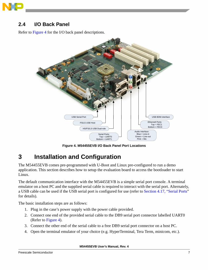
2.4 I/O Back PanelRefer to Figure 4 for the I/O back panel descriptions.
Figure 4. M54455EVB I/O Back Panel Port Locations
3 Installation and ConfigurationThe M54455EVB comes pre-programmed with U-Boot and Linux pre-configured to run a demo application. This section describes how to setup the evaluation board to access the bootloader to start Linux.
The default communication interface with the M54455EVB is a simple serial port console. A terminal emulator on a host PC and the supplied serial cable is required to interact with the serial port. Alternately, a USB cable can be used if the USB serial port is configured for use (refer to Section 4.17, “Serial Ports” for details).
The basic installation steps are as follows:1. Plug in the case’s power supply with the power cable provided.2. Connect one end of the provided serial cable to the DB9 serial port connector labelled UART0
(Refer to Figure 4).3. Connect the other end of the serial cable to a free DB9 serial port connector on a host PC.4. Open the terminal emulator of your choice (e.g. HyperTerminal, Tera Term, minicom, etc.).
USB Serial Port
FS/LS USB Host
HS/FS/LS USB Dual-role
Serial Ports: Top = UART0 Bottom = UART1
Audio Interface: Blue = Line-in
Green = Line-outPink = Mic
Ethernetl Ports: Top = FEC1 Bottom = FEC0
USB BDM interface
M54455EVB User’s Manual, Rev. 4
Freescale Semiconductor 7

5. Configure the COM port as follows:
6. Press the power switch on the front of the computer case and the U-Boot banner (example below) should appear in the terminal window.
U-Boot 1.2.0-g4a442d31-dirty (Aug 23 2007 - 11:14:19)
CPU: Freescale MCF54455 (Mask:48 Version:1) CPU CLK 266 Mhz BUS CLK 133 Mhz FLB CLK 33 Mhz INP CLK 33 Mhz VCO CLK 533 MhzBoard: Freescale M54455 EVBI2C: readyDRAM: 256 MBFLASH: 16.5 MBIn: serialOut: serialErr: serialNet: FEC0, FEC1IDE: Bus 0: not available Status = 0x60->
Linux and a root file system are preprogrammed into the second Flash device (Flash1) at address 0x0000_0000. A demo application automatically runs when Linux is started. A network connection is required for the web server portion of the demo to work.
7. Plug one end of the provided Ethernet cable into a network or host PC with a DHCP server running. Plug the other end of the cable into the FEC0 interface (bottom RJ45 receptacle) of the M54455EVB.
8. To boot Linux, issue the following U-Boot command. -> bootm 0
9. The demo application prints out a banner message including the IP address that it obtained from the DHCP server. Launch a web client (e.g. Firefox or Internet Explorer) and copy this IP address into the web browser. The M54455EVB serves up a web page with more information on the available demos.
4 Hardware SubmodulesThe following sections describe the hardware submodules of the M54455EVB.
Table 2. Default Serial Console Settings
Parameter Setting
Baud Rate 115,200 bps
Data bits 8
Parity None
Stop bits 1
Flow Control None or Software (Xon/Xoff)
M54455EVB User’s Manual, Rev. 4
8 Freescale Semiconductor
4.1 DDR SDRAM InterfaceThe MCF5445x DDR SDRAM controller has the following features:
• Supports a glueless interface to DDR, DDR2, and mobile/low-power DDR SDRAM devices• Support for 16-bit fixed memory port width• 16-byte critical word first burst transfer• Up to 14 lines of row address, up to 11 column address lines, 2 bits of bank address, and two chip
selects.• Supports up to 512 MByte of memory; minimum memory configuration of 8 MByte• Supports page mode to maximize the data rate• Supports sleep mode and self-refresh mode
The M54455EVB features 256 MBytes of DDR2 SDRAM. Four 8-bit wide Micron MT47H64M8 (512 Mbit) devices are arranged as two 16 M × 8 × 4 banks per SDRAM controller chip select. This results in two 16-bit wide, 128 MBytes blocks of DDR2 memory
The SDRAM interface is terminated with parallel termination resistors. The MCF5445x does not provide control for the DDR2 on-die termination. The ODT pins on the DDR2 devices are connected to control signals from the CPLD for test purposes only. These signals are disabled in the normal functional mode.
4.2 Reset ControllerThe reset controller on the M54455EVB is implemented in a Xilinx XC95144XL CPLD. The CPLD controls the state of the system reset signal (SYSRESET) gathers reset information from a pushbutton reset (SW2), the BDM interface, and the FPGA (FPGA_DONE). At system power-on, the CPLD holds SYSRESET asserted until the FPGA has loaded its image from the platform flash PROM and asserted the FPGA_DONE signal. After system power-on, the CPLD asserts SYSRESET when it detects the assertion of any of the reset sources.
4.3 MCF5445x Boot OptionsDuring a system reset, the CPLD also drives the boot mode configuration signals into the MCF5445x. The MCF5445x has three boot mode options:
• Boot with default configuration constants specified in the RCON register, • Boot with configuration data specified by the Flexbus FB_AD[7:0] pins, and • Boot with configuration data obtained from an external SPI memory through the serial boot
facility.
In all of these cases, the boot code is fetched from an external memory connected to the Flexbus on FB_CS0 with the possible exception of the serial boot mode. In serial boot mode, if the boot load length field (BLL) in the reset configuration data stored in the SPI memory is non-zero, then boot code is loaded from the SPI memory instead of from Flexbus.
The MCF5445x boot mode is determined by the state of the BOOTMOD[1:0] input pins during the rising edge of RSTOUT (MCF5445x reset output signal). The CPLD drives BOOTMOD[1:0] to the values that
M54455EVB User’s Manual, Rev. 4
Freescale Semiconductor 9
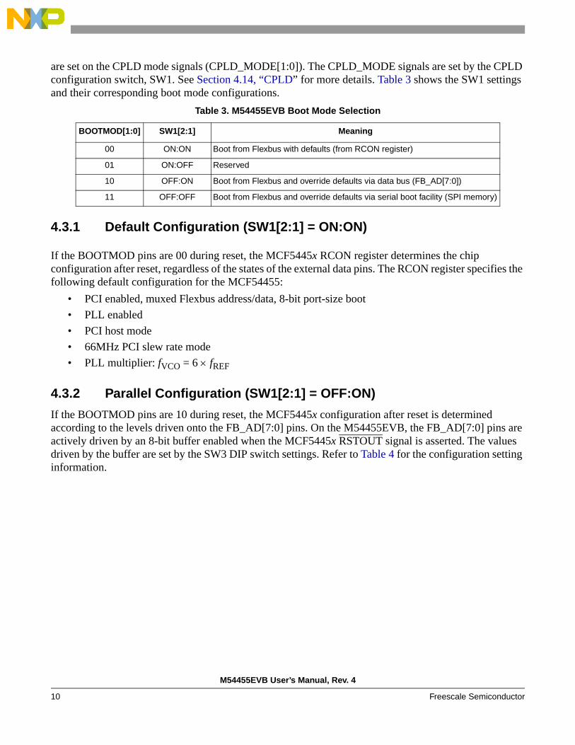
are set on the CPLD mode signals (CPLD_MODE[1:0]). The CPLD_MODE signals are set by the CPLD configuration switch, SW1. See Section 4.14, “CPLD” for more details. Table 3 shows the SW1 settings and their corresponding boot mode configurations.
4.3.1 Default Configuration (SW1[2:1] = ON:ON)
If the BOOTMOD pins are 00 during reset, the MCF5445x RCON register determines the chip configuration after reset, regardless of the states of the external data pins. The RCON register specifies the following default configuration for the MCF54455:
• PCI enabled, muxed Flexbus address/data, 8-bit port-size boot• PLL enabled• PCI host mode• 66MHz PCI slew rate mode• PLL multiplier: fVCO = 6 × fREF
4.3.2 Parallel Configuration (SW1[2:1] = OFF:ON)
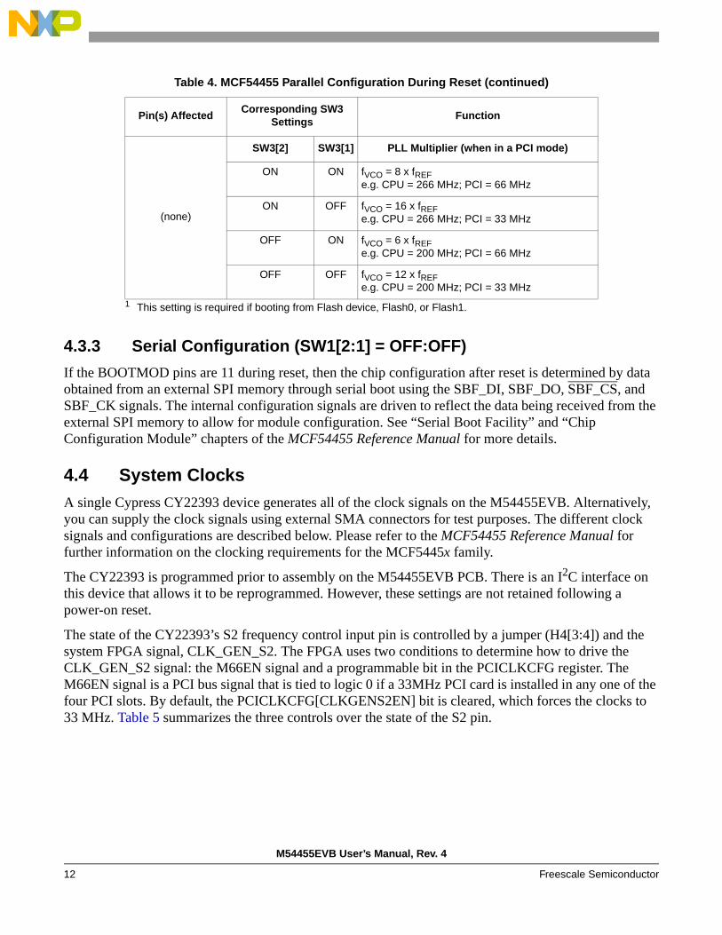
If the BOOTMOD pins are 10 during reset, the MCF5445x configuration after reset is determined according to the levels driven onto the FB_AD[7:0] pins. On the M54455EVB, the FB_AD[7:0] pins are actively driven by an 8-bit buffer enabled when the MCF5445x RSTOUT signal is asserted. The values driven by the buffer are set by the SW3 DIP switch settings. Refer to Table 4 for the configuration setting information.
Table 3. M54455EVB Boot Mode Selection
BOOTMOD[1:0] SW1[2:1] Meaning
00 ON:ON Boot from Flexbus with defaults (from RCON register)
01 ON:OFF Reserved
10 OFF:ON Boot from Flexbus and override defaults via data bus (FB_AD[7:0])
11 OFF:OFF Boot from Flexbus and override defaults via serial boot facility (SPI memory)
M54455EVB User’s Manual, Rev. 4
10 Freescale Semiconductor

Table 4. MCF54455 Parallel Configuration During Reset
Pin(s) AffectedCorresponding SW3
SettingsFunction
FB_AD[31:0], PCI_*
SW3[8] SW3[7] SW3[6] Flexbus, PCI, Port Size Mode
ON ON ON PCI, muxed FB addr/data, 8-bit boot1
ON ON OFF No PCI, muxed FB addr/data, 16-bit boot
ON OFF ON No PCI, muxed FB addr/data, 8-bit boot
ON OFF OFF No PCI, muxed FB addr/data, 32-bit boot
OFF ON ON PCI, muxed FB addr/data, 16-bit boot
OFF ON OFF No PCI, non-muxed FB addr/data, 16-bit boot
OFF OFF ON No PCI, non-muxed FB addr/data, 8-bit boot
OFF OFF OFF No PCI, non-muxed FB addr/data, 32-bit boot
Output Clocks
SW3[5] PLL Mode
ON Limp mode
OFF PLL mode
(none)
SW3[4] PCI Host/Agent Mode (when in a PCI mode)
ON PCI host mode
OFF PCI agent mode
(none)
SW3[4] Oscillator Mode (when in a No PCI mode)
ON Oscillator bypass mode
OFF Crystal oscillator mode
PCI_*
SW3[3] PCI Slew Rate Mode (when in a PCI mode)
ON 66 MHz slew rate mode
OFF 33 MHz slew rate mode
(none)
SW3[3] SW3[2] SW3[1] PLL Multiplier (when in a No PCI mode)
ON ON ON fVCO = 8 x fREF
ON ON OFF fVCO = 16 x fREF
ON OFF ON fVCO = 6 x fREF
ON OFF OFF fVCO = 12 x fREF
OFF ON ON fVCO = 18 x fREF
OFF ON OFF fVCO = 24 x fREF
OFF OFF ON fVCO = 10 x fREF
OFF OFF OFF fVCO = 20 x fREF
M54455EVB User’s Manual, Rev. 4
Freescale Semiconductor 11
4.3.3 Serial Configuration (SW1[2:1] = OFF:OFF)
If the BOOTMOD pins are 11 during reset, then the chip configuration after reset is determined by data obtained from an external SPI memory through serial boot using the SBF_DI, SBF_DO, SBF_CS, and SBF_CK signals. The internal configuration signals are driven to reflect the data being received from the external SPI memory to allow for module configuration. See “Serial Boot Facility” and “Chip Configuration Module” chapters of the MCF54455 Reference Manual for more details.
4.4 System ClocksA single Cypress CY22393 device generates all of the clock signals on the M54455EVB. Alternatively, you can supply the clock signals using external SMA connectors for test purposes. The different clock signals and configurations are described below. Please refer to the MCF54455 Reference Manual for further information on the clocking requirements for the MCF5445x family.
The CY22393 is programmed prior to assembly on the M54455EVB PCB. There is an I2C interface on this device that allows it to be reprogrammed. However, these settings are not retained following a power-on reset.
The state of the CY22393’s S2 frequency control input pin is controlled by a jumper (H4[3:4]) and the system FPGA signal, CLK_GEN_S2. The FPGA uses two conditions to determine how to drive the CLK_GEN_S2 signal: the M66EN signal and a programmable bit in the PCICLKCFG register. The M66EN signal is a PCI bus signal that is tied to logic 0 if a 33MHz PCI card is installed in any one of the four PCI slots. By default, the PCICLKCFG[CLKGENS2EN] bit is cleared, which forces the clocks to 33 MHz. Table 5 summarizes the three controls over the state of the S2 pin.
(none)
SW3[2] SW3[1] PLL Multiplier (when in a PCI mode)
ON ON fVCO = 8 x fREFe.g. CPU = 266 MHz; PCI = 66 MHz
ON OFF fVCO = 16 x fREFe.g. CPU = 266 MHz; PCI = 33 MHz
OFF ON fVCO = 6 x fREFe.g. CPU = 200 MHz; PCI = 66 MHz
OFF OFF fVCO = 12 x fREFe.g. CPU = 200 MHz; PCI = 33 MHz
1 This setting is required if booting from Flash device, Flash0, or Flash1.
Table 4. MCF54455 Parallel Configuration During Reset (continued)
Pin(s) AffectedCorresponding SW3
SettingsFunction
M54455EVB User’s Manual, Rev. 4
12 Freescale Semiconductor
The following pseudocode illustrates the input clock determination logic:if ((H4[3:4] shunt is not installed) and
(no 33MHz PCI cards installed (M66EN logic 1)) and(FPGA_PCICLKCFG[CLKGENS2EN] is set))
{S2 = 1; PCI Clocks and MCF5445x input clock are 66MHz
}else{
S2 = 0; PCI Clocks and MCF5445x input clock are 33MHz}
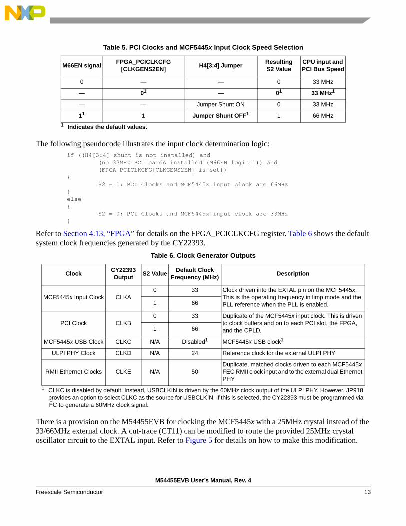
Refer to Section 4.13, “FPGA” for details on the FPGA_PCICLKCFG register. Table 6 shows the default system clock frequencies generated by the CY22393.
There is a provision on the M54455EVB for clocking the MCF5445x with a 25MHz crystal instead of the 33/66MHz external clock. A cut-trace (CT11) can be modified to route the provided 25MHz crystal oscillator circuit to the EXTAL input. Refer to Figure 5 for details on how to make this modification.
Table 5. PCI Clocks and MCF5445x Input Clock Speed Selection
M66EN signalFPGA_PCICLKCFG
[CLKGENS2EN]H4[3:4] Jumper
ResultingS2 Value
CPU input and PCI Bus Speed
0 — — 0 33 MHz
— 01
1 Indicates the default values.
— 01 33 MHz1
— — Jumper Shunt ON 0 33 MHz
11 1 Jumper Shunt OFF1 1 66 MHz
Table 6. Clock Generator Outputs
ClockCY22393Output
S2 ValueDefault Clock
Frequency (MHz)Description
MCF5445x Input Clock CLKA0 33 Clock driven into the EXTAL pin on the MCF5445x.
This is the operating frequency in limp mode and the PLL reference when the PLL is enabled. 1 66
PCI Clock CLKB0 33 Duplicate of the MCF5445x input clock. This is driven
to clock buffers and on to each PCI slot, the FPGA, and the CPLD.1 66
MCF5445x USB Clock CLKC N/A Disabled1
1 CLKC is disabled by default. Instead, USBCLKIN is driven by the 60MHz clock output of the ULPI PHY. However, JP918 provides an option to select CLKC as the source for USBCLKIN. If this is selected, the CY22393 must be programmed via I2C to generate a 60MHz clock signal.
MCF5445x USB clock1
ULPI PHY Clock CLKD N/A 24 Reference clock for the external ULPI PHY
RMII Ethernet Clocks CLKE N/A 50Duplicate, matched clocks driven to each MCF5445x FEC RMII clock input and to the external dual Ethernet PHY
M54455EVB User’s Manual, Rev. 4
Freescale Semiconductor 13

Figure 5. MCF5445x Input Clock Selection Cut-Trace
4.5 SPI FlashA 16 Mbit SPI flash is connected to the MCF5445x via the DSPI interface. This same SPI flash can be used to store reset configuration parameters and boot code when using the serial boot facility. Refer to Section 4.3, “MCF5445x Boot Options” for more information on how to configure the M54455EVB for serial boot.
4.6 FlashThe M54455EVB features two flash devices connected to the FlexBus expansion bus. The smaller of the two flashes is a 512KByte, 8-bit wide AT49BV040 (or compatible) device referred to as Flash0. This device contains the U-Boot bootloader. The larger of the two flashes is a 16 MByte, 8-bit wide 28F128J3D (or compatible) device referred to as Flash1. By default, this flash device is programmed with a Linux image, but it can be reprogrammed and used as a boot device if desired.
The selection of a boot flash device is achieved with a CPLD mode switch setting, specifically CPLD_MODE2 which is controllable by DIP switch SW1[3]. The device that is connected to the global chip-select from the MCF5445x (FB_CS0) is the boot device. The other device is connected to FB_CS1. Table 7 shows the boot device selection settings.
Table 7. Flash Chip Select Configuration
SW1[3] Meaning Application
OFFFlash1 is the boot deviceFLASH1_CS = FB_CS0FLASH0_CS = FB_CS1
Boot custom image
ONFlash0 is the boot deviceFLASH1_CS = FB_CS1FLASH0_CS = FB_CS0
Boot U-Boot
cut trace
solder
M54455EVB User’s Manual, Rev. 4
14 Freescale Semiconductor

4.7 PCIThe MCF5445x processor's PCI controller module has the following features:
• Compatible with PCI 2.2 specification• Supports up to four external PCI masters• 32-bit target and initiator operation• 33–66 MHz operation with PCI bus to internal bus divider ratios of 1:1, 1:2, 1:3, 2:3, 1:4, and 1:5.• Support for host and agent configurations.
The M54455EVB is designed to feature the MCF5445x as a PCI host. It provides four, 32-bit, 3.3V PCI slots. The IDSEL pins on each of the slots and the MCF5445x is connected to a different PCI_AD signal. Table 8 shows the IDSEL connections.
4.7.1 PCI Clocking
The MCF5445x does not output a PCI clock. The PCI controller of the MCF5445x is timed to the input reference clock on EXTAL. Therefore, the input reference clock to the MCF5445x is matched to each of the PCI slots on the M54455EVB to maintain clock phase alignment and ensure proper PCI timings.
The M54455EVB is designed to support 33- and 66-MHz 32-bit PCI cards. However, the speed of the PCI clocks and input clock is limited to that of the slowest device by logic on the M54455EVB. The frequency of these clocks is controlled by an input (S2) into the clock generator logic. The FPGA automatically adjusts this control signal based on the M66EN signal from each PCI slot. The S2 signal is also controllable by a jumper and a memory mapped register in the FPGA. See Section 4.4, “System Clocks” and Section 4.13, “FPGA” for more information. Table 5 provides a summary of the PCI bus speed controls.
4.7.2 PCI Power
The PCI is only available if an ATX supply is used to power the board. If the optional barrel power connector is used, then the ATX3V3 supply is not available. This also affects the clocking of the MCF5445x. The M66EN signal is pulled-up to the ATX3V3 supply. Without this supply, the M66EN signal is detected as a logic 0 and the CPU input reference frequency is forced to 33MHz.
Table 8. PCI IDSEL Assignments
PCI Slot IDSEL Assignment
Slot 0 PCI_AD17
Slot 1 PCI_AD18
Slot 2 PCI_AD19
Slot 3 PCI_AD20
MCF5445x PCI_AD16
M54455EVB User’s Manual, Rev. 4
Freescale Semiconductor 15

4.7.3 PCI Arbitration
By default, the EVB uses the MCF5445x on-chip PCI arbiter, and the request/grant signals from the PCI slots are routed directly to the MCF5445x. The board does provide cut-trace options to allow you to route these PCI arbitration signals to the FPGA. It would then be left to you to implement an external arbitration scheme in the FPGA.
The following figures describe how to alter the M54455EVB to route the PCI arbitration signals to the FPGA. Reference designators for the cut-trace board footprints are CT1-CT10. CT1-CT2, CT5-CT7 and CT9 can be found near the PCI slots (J14, J15, J16, J17), and CT8, CT10, CT3 and CT4 can be found near the MCF5445x (U1).
Figure 6. PCI Request 0 Cut Trace Option—Use FPGA for Arbitration
M54455EVB User’s Manual, Rev. 4
16 Freescale Semiconductor

Figure 7. PCI Request 1 and Request 2 Cut Trace Option—Use FPGA for Arbitration
Figure 8. PCI Request 3 Cut Trace Option—Use FPGA for Arbitration
M54455EVB User’s Manual, Rev. 4
Freescale Semiconductor 17
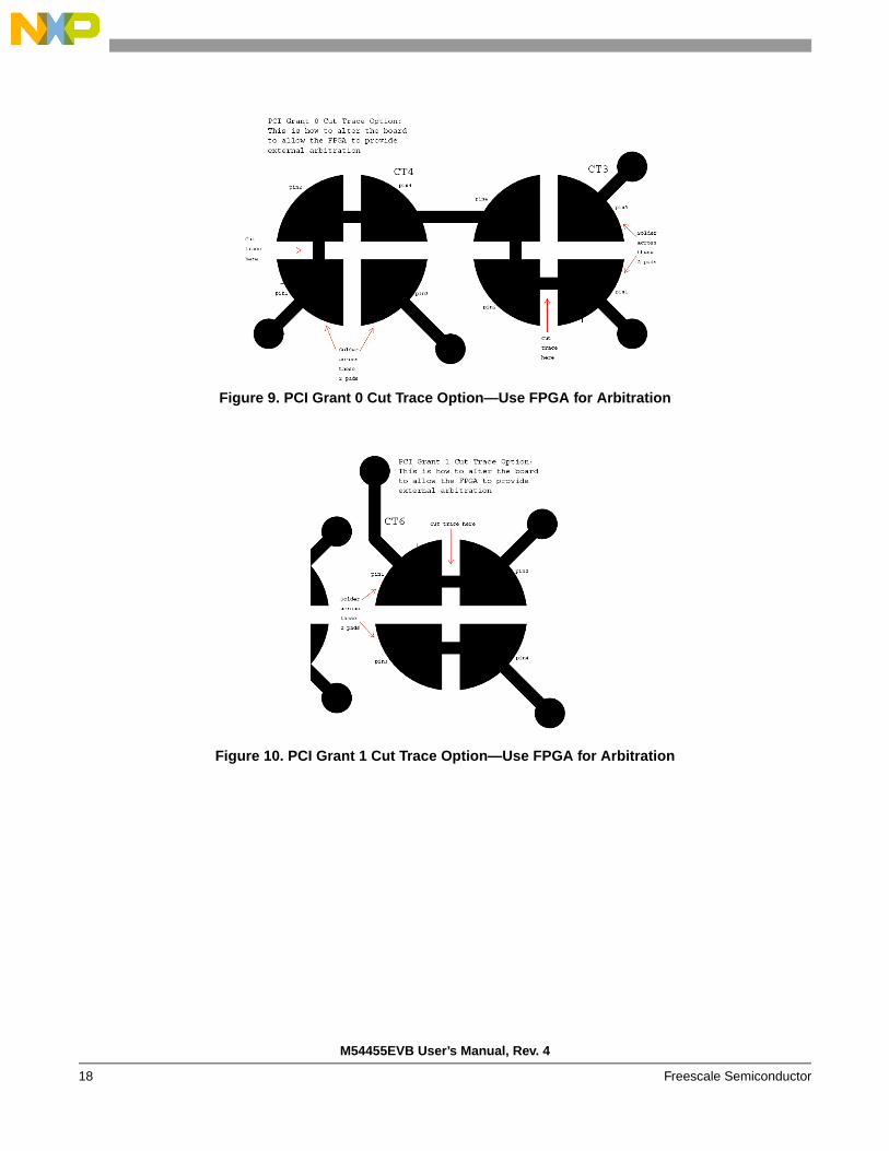
Figure 9. PCI Grant 0 Cut Trace Option—Use FPGA for Arbitration
Figure 10. PCI Grant 1 Cut Trace Option—Use FPGA for Arbitration
M54455EVB User’s Manual, Rev. 4
18 Freescale Semiconductor
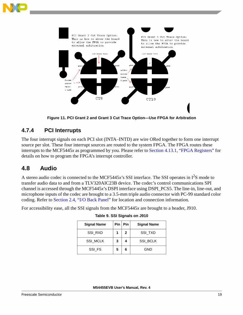
Figure 11. PCI Grant 2 and Grant 3 Cut Trace Option—Use FPGA for Arbitration
4.7.4 PCI Interrupts
The four interrupt signals on each PCI slot (INTA–INTD) are wire ORed together to form one interrupt source per slot. These four interrupt sources are routed to the system FPGA. The FPGA routes these interrupts to the MCF5445x as programmed by you. Please refer to Section 4.13.1, “FPGA Registers” for details on how to program the FPGA’s interrupt controller.
4.8 AudioA stereo audio codec is connected to the MCF5445x’s SSI interface. The SSI operates in I2S mode to transfer audio data to and from a TLV320AIC23B device. The codec’s control communications SPI channel is accessed through the MCF5445x’s DSPI interface using DSPI_PCS5. The line-in, line-out, and microphone inputs of the codec are brought to a 3.5-mm triple audio connector with PC-99 standard color coding. Refer to Section 2.4, “I/O Back Panel” for location and connection information.
For accessibility ease, all the SSI signals from the MCF5445x are brought to a header, J910.Table 9. SSI Signals on J910
Signal Name Pin Pin Signal Name
SSI_RXD 1 2 SSI_TXD
SSI_MCLK 3 4 SSI_BCLK
SSI_FS 5 6 GND
M54455EVB User’s Manual, Rev. 4
Freescale Semiconductor 19

4.9 BDM and JTAGThe primary debug port on the MCF5445x is referred to as the background debug module or BDM. The standard 26-pin BDM header (J24) is provided on the M54455EVB for attachment of an external BDM control interface. However, the M54455EVB also features a built-in P&E USB ColdFire Multilink. This interface is brought out to the I/O back panel to a standard Type-B USB receptacle. Refer to Section 2.4, “I/O Back Panel” for the location of the connector. This allows for run-control debugging with a standard USB cable (provided in the M54455EVB kit).
The MCF5445x also features IEEE 1149.1 Test Access Port (JTAG) test logic that can be used for boundary-scan testability. The access pins for JTAG are multiplexed over the BDM control signals and are available on J24.
The JTAG_EN input signal to the MCF5445x determines the debug mode: BDM or JTAG. This signal is controllable by JP903 as shown below.
The TCLK and PSTCLK signals are the only two multiplexed signals that switch input/output state depending on which debug mode is selected. In BDM mode, the PSTCLK is an output from the MCF5445x to the external BDM control interface. In JTAG mode, TCLK is the test clock input. The standard 26-pin BDM header defines pin 24 as PSTCLK. A common practice is to place TCLK on pin 6 of this header. JP904 is available to control the routing of the multiplexed TCLK_PSTCLK signal to the 26-pin debug header (J24) as shown below.
Table 10. Debug Mode Selection
JP903 Setting Debug Mode
Shunt on 1-2 JTAG
Shunt on 2-3 BDM
Table 11. TCLK/PSTCLK Routing Control
JP904 Setting TCLK_PSTCLK Routing
Shunt on 1-2 TCLK/PSTCLK on J24[24]1
1 This setting is required if an external BDM control interface is used. If the on-board USB Multilink is used, this jumper setting is ignored.
Shunt on 2-3 TCLK/PSTCLK on J24[6]2
2 This pin was previously specified by Freescale as Developer Reserved. External BDM control cables may be able to make use of this pin for JTAG instructions. There is a 10-kΩ pull-down resistor on the TCK_PSTCLK signal when this setting is selected.
M54455EVB User’s Manual, Rev. 4
20 Freescale Semiconductor
4.10 USB The MCF5445x integrates a USB 2.0 dual-role module with the following features:
• Support for host and device modes• Support for full speed (FS) and low speed (LS) via an on-chip FS/LS transceiver• Optional UTMI+ Low Pin Count Interface (ULPI) to support high speed (HS) transfers as well as
FS and LS• Uses 60 MHz reference clock based off of the system clock or from an external pin
The M54455EVB provides two interfaces to the single MCF5445x USB controller. Only one of these interfaces can be used at any one time.
4.10.1 On-Chip FS/LS Transceiver
The on-chip FS/LS transceiver signals are brought out to a type-A USB connector and are intended to be used for USB host applications. 15-kΩ pull-down and 33-Ω series resistors are provided on the D+ and D- data signals. Power to the connector is provided by an external dual-channel power distribution switch (MIC2026-1YM, U928). The B-channel of this device supplies the power for the type-A connector and is controlled by the MCF5445x USB_VBUS_EN output control signal.
When the on-chip FS/LS transceiver is used, the ULPI PHY can be put into its reset state. Refer to Section 4.14, “CPLD” for details.
4.10.2 ULPI PHY
The ULPI interface of the MCF5445x is also featured on the M54455EVB. An external ULPI physical layer device, the SMSC USB3300 (U927), connects directly to the MCF5445x ULPI interface. The USB signals from the ULPI PHY are brought out to a mini-AB USB connector. The ID pin on the mini-AB connector connects to the ULPI PHY’s ID pin and indicates whether a host or device is connected. The ULPI PHY has an enable signal connected to the A-channel of the MIC2026 power distribution switch that is used to supply VBUS when operating as a host.
The RESET signal input to the ULPI PHY is controlled by the system’s CPLD. Refer to Section 4.14, “CPLD” for details.
4.11 EthernetThe MCF5445x processor features two Fast Ethernet controllers (FEC) with MII and RMII interface options. The M54455EVB provides a dual 10/100 Mbps Ethernet PHY to interface with the processor’s FECs. The PHY operates in dual RMII mode. The board also provides two RJ45 connectors with integrated magnetics and LEDs.
The dual-port 10/100 Mbps provides a power-down feature for each port. You can control these power down signals via the system’s CPLD.
M54455EVB User’s Manual, Rev. 4
Freescale Semiconductor 21
NOTEThe FEC1 RMII interface signals on the MCF5445x are multiplexed with the upper eight bits of the ATA data bus. You must select between using the FEC1 interface or the full ATA interface. The system’s CPLD provides control for this selection. Refer to Section 4.14, “CPLD” for details.
4.12 ATAThe M54455EVB provides a standard 40-pin ATA connector, as well as an external ATA data buffer that interfaces with the MCF5445x processor's ATA interface.
A device connected to the ATA Interface must be powered by a separate supply. Several peripheral power connectors are provided by the ATX power supply inside the case of the M54455EVB.
NOTESome of the ATA interface signals on the MCF5445x are multiplexed with the FEC1 RMII interface signals. To have access to the full 16-bit ATA data bus, the FEC1 interface must be disabled. The system’s CPLD provides control for this selection. Refer to Section 4.14, “CPLD” for details.
4.13 FPGAThe M54455EVB FPGA is a Xilinx Spartan 3 FPGA that provides interrupt control for the four PCI slots and the pushbuttons SW6 and SW7. It also provides a buffered FlexBus interface to the external 256K × 16bit MRAM and an interface to a seven-segment display and two LEDs.
4.13.1 FPGA Registers
The FPGA implements several FlexBus accessible memory-mapped registers. Table 12 shows the memory map and the following sections provide details on each register.
NOTEUse only 32-bit reads and writes to these registers.
Table 12. FPGA Memory Map
Address RegisterWidth(bits)
Access Reset Value Section/Page
0x0900_0000 FPGA interrupt request enable register (FPGA_IRQEN) 32 R/W 0x0000_0000 4.13.1.1/23
0x0900_0004 FPGA interrupt request status register (FPGA_IRQSTATUS) 32 R 0x0000_0000 4.13.1.2/23
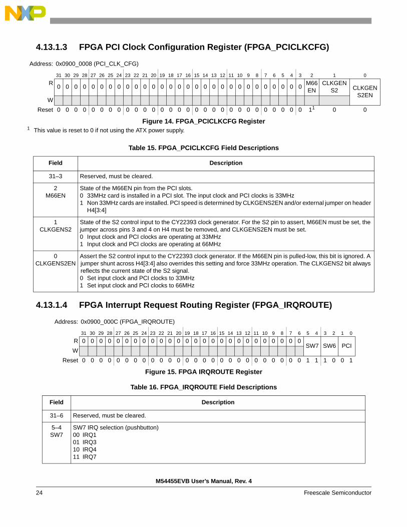
0x0900_0008 FPGA PCI clock configuration register (FPGA_PCICLKCFG) 32 R/W 0x0000_0004 4.13.1.3/24
0x0900_000C FPGA interrupt request routing register (FPGA_IRQROUTE) 32 R/W 0x0000_0039 4.13.1.4/24
0x0900_0010 FPGA version register (FPGA_VERSION) 32 R 0x1A00_0102 4.13.1.5/25
0x0900_0014 FPGA seven segment display register (FPGA_7SEGMENT) 32 R/W 0x0000_0000 4.13.1.6/26
0x0900_0018 FPGA LED control register (FPGA_LEDS) 32 R/W 0x0000_0000 4.13.1.7/26
M54455EVB User’s Manual, Rev. 4
22 Freescale Semiconductor
4.13.1.1 FPGA Interrupt Request Enable Register (FPGA_IRQEN)Q
4.13.1.2 FPGA Interrupt Request Status Register (FPGA_IRQSTATUS)
Address: 0x0900_0000 (FPGA_IRQEN)
31 30 29 28 27 26 25 24 23 22 21 20 19 18 17 16 15 14 13 12 11 10 9 8 7 6 5 4 3 2 1 0
R 0 0 0 0 0 0 0 0 0 0 0 0 0 0 0 0 0 0 0 0 0 0 0 0 0 0SW7 SW6 PCI
W
Reset 0 0 0 0 0 0 0 0 0 0 0 0 0 0 0 0 0 0 0 0 0 0 0 0 0 0 0 0 0 0 0 0
Figure 4-12. FPGA_IRQEN Register
Table 13. FPGA_IRQEN Field Descriptions
Field Description
31–6 Reserved, must be cleared.
5SW7
Setting this bit allows the SW7 pushbutton interrupt source to be passed through to the IRQ line determined by FPGA_IRQROUTE.1 SW7 interrupt is enabled0 SW7 interrupt source does not assert an IRQ
4SW6
Setting this bit allows the SW6 pushbutton interrupt source to be passed through to the IRQ line determined by FPGA_IRQROUTE.1 SW6 interrupt is enabled0 SW6 interrupt source does not assert an IRQ
3–0PCI
Setting these bits allow the corresponding PCI interrupt source to be passed through to the IRQ line determined by FPGA_IRQROUTE.1 Corresponding PCI interrupt is enabled0 Corresponding PCI interrupt source does not assert an IRQ
Address: 0x0900_0004 (FPGA_IRQSTATUS)
31 30 29 28 27 26 25 24 23 22 21 20 19 18 17 16 15 14 13 12 11 10 9 8 7 6 5 4 3 2 1 0
R 0 0 0 0 0 0 0 0 0 0 0 0 0 0 0 0 0 0 0 0 0 0 0 0 0 0 SW7 SW6 PCI
W
Reset 0 0 0 0 0 0 0 0 0 0 0 0 0 0 0 0 0 0 0 0 0 0 0 0 0 0 0 0 0 0 0 0
Figure 13. FPGA_IRQSTATUS Register
Table 14. FPGA_IRQSTATUS Field Descriptions
Field Description
31–6 Reserved, must be cleared.
5SW7
Indicates the SW7_b signal is asserted. This bit shows the status of the interrupt, even if FPGA_IRQEN[SW7] is cleared.
4SW6
Indicates the SW6_b signal is asserted. This bit shows the status of the interrupt, even if FPGA_IRQEN[SW6] is cleared.
3–0PCI
Indicates the corresponding interrupt PCI_IRQ line is asserted. These bits show the status of interrupt, even if the corresponding FPGA_IRQEN[PCI] bit is cleared.
M54455EVB User’s Manual, Rev. 4
Freescale Semiconductor 23
A
1
4.13.1.3 FPGA PCI Clock Configuration Register (FPGA_PCICLKCFG)
4.13.1.4 FPGA Interrupt Request Routing Register (FPGA_IRQROUTE)
ddress: 0x0900_0008 (PCI_CLK_CFG)
31 30 29 28 27 26 25 24 23 22 21 20 19 18 17 16 15 14 13 12 11 10 9 8 7 6 5 4 3 2 1 0
R0 0 0 0 0 0 0 0 0 0 0 0 0 0 0 0 0 0 0 0 0 0 0 0 0 0 0 0 0
M66EN
CLKGENS2 CLKGEN
S2ENW
Reset 0 0 0 0 0 0 0 0 0 0 0 0 0 0 0 0 0 0 0 0 0 0 0 0 0 0 0 0 0 11
This value is reset to 0 if not using the ATX power supply.
0 0
Figure 14. FPGA_PCICLKCFG Register
Table 15. FPGA_PCICLKCFG Field Descriptions
Field Description
31–3 Reserved, must be cleared.
2M66EN
State of the M66EN pin from the PCI slots.0 33MHz card is installed in a PCI slot. The input clock and PCI clocks is 33MHz1 Non 33MHz cards are installed. PCI speed is determined by CLKGENS2EN and/or external jumper on header
H4[3:4]
1CLKGENS2
State of the S2 control input to the CY22393 clock generator. For the S2 pin to assert, M66EN must be set, the jumper across pins 3 and 4 on H4 must be removed, and CLKGENS2EN must be set.0 Input clock and PCI clocks are operating at 33MHz1 Input clock and PCI clocks are operating at 66MHz
0CLKGENS2EN
Assert the S2 control input to the CY22393 clock generator. If the M66EN pin is pulled-low, this bit is ignored. A jumper shunt across H4[3:4] also overrides this setting and force 33MHz operation. The CLKGENS2 bit always reflects the current state of the S2 signal.0 Set input clock and PCI clocks to 33MHz1 Set input clock and PCI clocks to 66MHz
Address: 0x0900_000C (FPGA_IRQROUTE)
31 30 29 28 27 26 25 24 23 22 21 20 19 18 17 16 15 14 13 12 11 10 9 8 7 6 5 4 3 2 1 0
R 0 0 0 0 0 0 0 0 0 0 0 0 0 0 0 0 0 0 0 0 0 0 0 0 0 0SW7 SW6 PCI
W
Reset 0 0 0 0 0 0 0 0 0 0 0 0 0 0 0 0 0 0 0 0 0 0 0 0 0 0 1 1 1 0 0 1
Figure 15. FPGA IRQROUTE Register
Table 16. FPGA_IRQROUTE Field Descriptions
Field Description
31–6 Reserved, must be cleared.
5–4SW7
SW7 IRQ selection (pushbutton)00 IRQ101 IRQ310 IRQ411 IRQ7
M54455EVB User’s Manual, Rev. 4
24 Freescale Semiconductor

4.13.1.5 FPGA Version Register (FPGA_VERSION)
The FPGA_VERSION register reflects the version of the FPGA code image.
3–2SW6
SW6 IRQ selection (pushbutton)00 IRQ101 IRQ310 IRQ411 IRQ7
1–0PCI
PCI IRQ selection00 IRQ101 IRQ310 IRQ411 IRQ7
Address: 0x0900_0010 (FPGA_VERSION)
31 30 29 28 27 26 25 24 23 22 21 20 19 18 17 16 15 14 13 12 11 10 9 8 7 6 5 4 3 2 1 0
R BUILD_WW 0 0 0 0 0 0 0 0 MAJOR_REV MINOR_REV
W
Reset 0 0 0 1 1 0 1 0 0 0 0 0 0 0 0 0 0 0 0 0 0 0 0 1 0 0 0 0 0 0 1 0
Figure 16. FPGA Version Register
Table 17. FPGA_VERSION Field Descriptions
Field Description
31–24BUILD_WW
Build date work week
23–16 Reserved, must be cleared.
15–8MAJOR_REV
Major revision number.Example: Revision 1.2 of the FPGA code. MAJOR_REV = 0x01, MINOR_REV = 0x02
7–0MINOR_REV
Minor revision number.Example: Revision 1.2 of the FPGA code. MAJOR_REV = 0x01, MINOR_REV = 0x02
Table 16. FPGA_IRQROUTE Field Descriptions (continued)
Field Description
M54455EVB User’s Manual, Rev. 4
Freescale Semiconductor 25

4.13.1.6 FPGA Seven Segment Display Register (FPGA_7SEGMENT)
4.13.1.7 FPGA LED Control Register (FPGA_LEDS)
4.14 CPLDA Xilinx XC95144XL CPLD performs a number of tasks on the M54455EVB including:
• Reset control• Boot mode selection• Peripheral multiplexing and enable/disable control• LED control• Board revision determination
Address: 0x0900_0014 (FPGA_7SEGMENT)
31 30 29 28 27 26 25 24 23 22 21 20 19 18 17 16 15 14 13 12 11 10 9 8 7 6 5 4 3 2 1 0
R 0 0 0 0 0 0 0 0 0 0 0 0 0 0 0 0 0 0 0 0 0 0 0 0LED
W
Reset 0 0 0 0 0 0 0 0 0 0 0 0 0 0 0 0 0 0 0 0 0 0 0 0 0 0 0 0 0 0 0 0
Figure 17. FPGA_7SEGMENT Register
Table 18. FPGA_7SEGMENT Field Descriptions
Field Description
31–8 Reserved, must be cleared.
7–0LED
Indicates the hex number you want to display on the 7-segment LED display (U28 on the EVB).
Address: 0x0900_0018 (FPGA_LEDS)
31 30 29 28 27 26 25 24 23 22 21 20 19 18 17 16 15 14 13 12 11 10 9 8 7 6 5 4 3 2 1 0
R 0 0 0 0 0 0 0 0 0 0 0 0 0 0 0 0 0 0 0 0 0 0 0 0 0 0 0 0 0 0LED2 LED1
W
Reset 0 0 0 0 0 0 0 0 0 0 0 0 0 0 0 0 0 0 0 0 0 0 0 0 0 0 0 0 0 0 0 0
Figure 18. FPGA LEDS Register
Table 19. FPGA_LEDS Field Descriptions
Field Description
31–2 Reserved, must be cleared.
1LED2
Controls the state of FPGA_LED2. FPGA_LED2 is reference designator D956.0 Off1 On
0LED1
Controls the state of FPGA_LED1. FPGA_LED1 is reference designator D957.0 Off1 On
M54455EVB User’s Manual, Rev. 4
26 Freescale Semiconductor
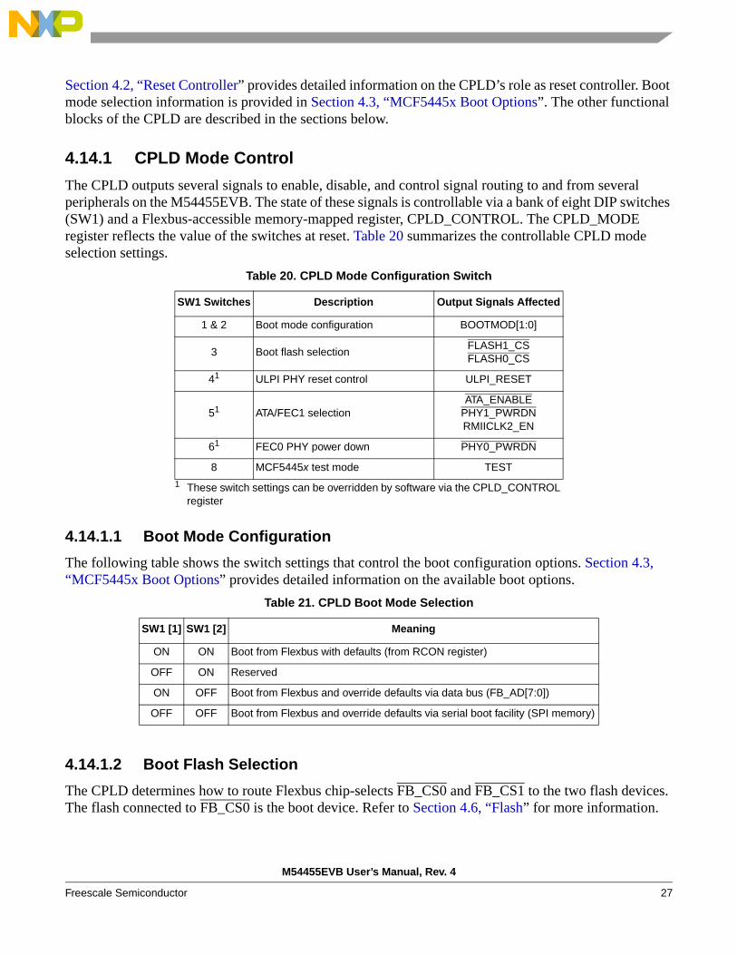
Section 4.2, “Reset Controller” provides detailed information on the CPLD’s role as reset controller. Boot mode selection information is provided in Section 4.3, “MCF5445x Boot Options”. The other functional blocks of the CPLD are described in the sections below.
4.14.1 CPLD Mode Control
The CPLD outputs several signals to enable, disable, and control signal routing to and from several peripherals on the M54455EVB. The state of these signals is controllable via a bank of eight DIP switches (SW1) and a Flexbus-accessible memory-mapped register, CPLD_CONTROL. The CPLD_MODE register reflects the value of the switches at reset. Table 20 summarizes the controllable CPLD mode selection settings.
4.14.1.1 Boot Mode Configuration
The following table shows the switch settings that control the boot configuration options. Section 4.3, “MCF5445x Boot Options” provides detailed information on the available boot options.
4.14.1.2 Boot Flash Selection
The CPLD determines how to route Flexbus chip-selects FB_CS0 and FB_CS1 to the two flash devices. The flash connected to FB_CS0 is the boot device. Refer to Section 4.6, “Flash” for more information.
Table 20. CPLD Mode Configuration Switch
SW1 Switches Description Output Signals Affected
1 & 2 Boot mode configuration BOOTMOD[1:0]
3 Boot flash selectionFLASH1_CSFLASH0_CS
41
1 These switch settings can be overridden by software via the CPLD_CONTROL register
ULPI PHY reset control ULPI_RESET
51 ATA/FEC1 selectionATA_ENABLE
PHY1_PWRDNRMIICLK2_EN
61 FEC0 PHY power down PHY0_PWRDN
8 MCF5445x test mode TEST
Table 21. CPLD Boot Mode Selection
SW1 [1] SW1 [2] Meaning
ON ON Boot from Flexbus with defaults (from RCON register)
OFF ON Reserved
ON OFF Boot from Flexbus and override defaults via data bus (FB_AD[7:0])
OFF OFF Boot from Flexbus and override defaults via serial boot facility (SPI memory)
M54455EVB User’s Manual, Rev. 4
Freescale Semiconductor 27
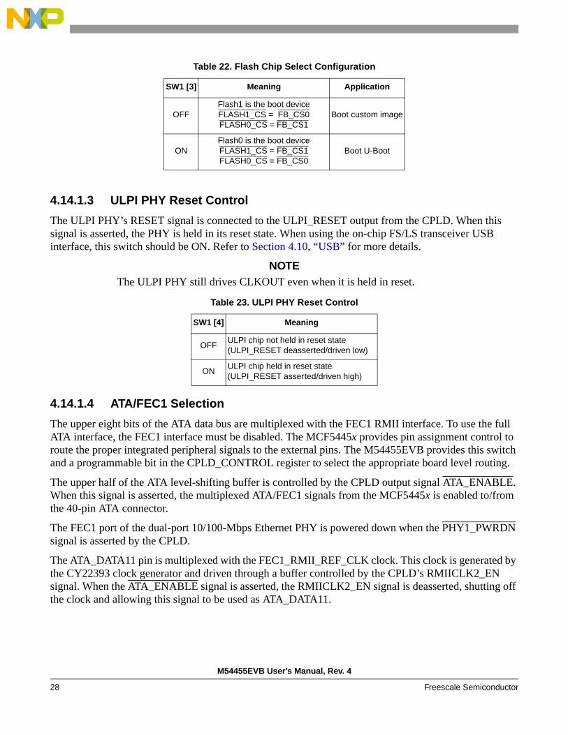
4.14.1.3 ULPI PHY Reset Control
The ULPI PHY’s RESET signal is connected to the ULPI_RESET output from the CPLD. When this signal is asserted, the PHY is held in its reset state. When using the on-chip FS/LS transceiver USB interface, this switch should be ON. Refer to Section 4.10, “USB” for more details.
NOTEThe ULPI PHY still drives CLKOUT even when it is held in reset.
4.14.1.4 ATA/FEC1 Selection
The upper eight bits of the ATA data bus are multiplexed with the FEC1 RMII interface. To use the full ATA interface, the FEC1 interface must be disabled. The MCF5445x provides pin assignment control to route the proper integrated peripheral signals to the external pins. The M54455EVB provides this switch and a programmable bit in the CPLD_CONTROL register to select the appropriate board level routing.
The upper half of the ATA level-shifting buffer is controlled by the CPLD output signal ATA_ENABLE. When this signal is asserted, the multiplexed ATA/FEC1 signals from the MCF5445x is enabled to/from the 40-pin ATA connector.
The FEC1 port of the dual-port 10/100-Mbps Ethernet PHY is powered down when the PHY1_PWRDN signal is asserted by the CPLD.
The ATA_DATA11 pin is multiplexed with the FEC1_RMII_REF_CLK clock. This clock is generated by the CY22393 clock generator and driven through a buffer controlled by the CPLD’s RMIICLK2_EN signal. When the ATA_ENABLE signal is asserted, the RMIICLK2_EN signal is deasserted, shutting off the clock and allowing this signal to be used as ATA_DATA11.
Table 22. Flash Chip Select Configuration
SW1 [3] Meaning Application
OFFFlash1 is the boot deviceFLASH1_CS = FB_CS0FLASH0_CS = FB_CS1
Boot custom image
ONFlash0 is the boot deviceFLASH1_CS = FB_CS1FLASH0_CS = FB_CS0
Boot U-Boot
Table 23. ULPI PHY Reset Control
SW1 [4] Meaning
OFFULPI chip not held in reset state(ULPI_RESET deasserted/driven low)
ONULPI chip held in reset state(ULPI_RESET asserted/driven high)
M54455EVB User’s Manual, Rev. 4
28 Freescale Semiconductor

4.14.1.5 FEC0 PHY Power Down
The FEC0 port of the dual-port 10/100-Mbps Ethernet PHY can be powered down by the CPLD’s PHY0_PWRDN signal. The default state of this signal is determined by SW1[6], but it can be overridden by the CPU via the CPLD_CONTROL register.
4.14.1.6 MCF5445x Test Mode
The MCF5445x test mode enable (active high) signal state is controlled by the CPLD’s TEST signal. The state of this signal is determined by SW1[8].
NOTETest mode is for Freescale test purposes only. Enabling test mode places the MCF5445x into a non-functional state.
4.14.2 M54455EVB Revision
Optionally populated resistors on the M54455EVB allow the revision to be indicated at the time of assembly. These resistors connections input to the CPLD, and the values can be read from CPLD_VERSION register. Refer to the description of the CPLD registers below.
Table 24. ATA/FEC1 Selection
SW1 [5] Meaning
OFF • Full ATA bus enabled (ATA_ENABLE asserted/driven low) • PHY1 powered down (PHY1_PWRDN asserted/driven low) • RMIICLK2 is disabled (RMIICLK2_EN deasserted/driven low)
ON • Upper 8 bits of the ATA data bus disabled (ATA_ENABLE deasserted/driven high) • PHY1 active (PHY1_PWRDN deasserted/driven high) • RMIICLK2 is enabled (RMIICLK2_EN asserted/driven high)
Table 25. FEC0 PHY Power Down
SW1 [6] Meaning
OFF PHY0 active (PHY0_PWRDN deasserted/driven high)
ON PHY0 powered down (PHY0_PWRDN asserted/driven low)
Table 26. MCF5445x Test Mode
SW1 [8] Meaning
OFF MCF5445x in normal function mode
ON MCF5445x in factory test modeNote: This setting is for Freescale use only and places the
MCF5445x into a non-functional mode.
M54455EVB User’s Manual, Rev. 4
Freescale Semiconductor 29
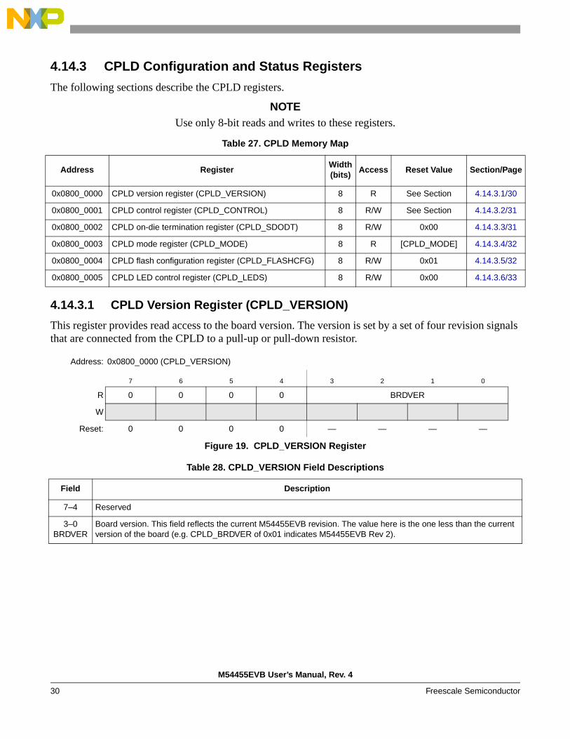
4.14.3 CPLD Configuration and Status Registers
The following sections describe the CPLD registers.
NOTEUse only 8-bit reads and writes to these registers.
4.14.3.1 CPLD Version Register (CPLD_VERSION)
This register provides read access to the board version. The version is set by a set of four revision signals that are connected from the CPLD to a pull-up or pull-down resistor.
Table 27. CPLD Memory Map
Address RegisterWidth(bits)
Access Reset Value Section/Page
0x0800_0000 CPLD version register (CPLD_VERSION) 8 R See Section 4.14.3.1/30
0x0800_0001 CPLD control register (CPLD_CONTROL) 8 R/W See Section 4.14.3.2/31
0x0800_0002 CPLD on-die termination register (CPLD_SDODT) 8 R/W 0x00 4.14.3.3/31
0x0800_0003 CPLD mode register (CPLD_MODE) 8 R [CPLD_MODE] 4.14.3.4/32
0x0800_0004 CPLD flash configuration register (CPLD_FLASHCFG) 8 R/W 0x01 4.14.3.5/32
0x0800_0005 CPLD LED control register (CPLD_LEDS) 8 R/W 0x00 4.14.3.6/33
Address: 0x0800_0000 (CPLD_VERSION)
7 6 5 4 3 2 1 0
R 0 0 0 0 BRDVER
W
Reset: 0 0 0 0 — — — —
Figure 19. CPLD_VERSION Register
Table 28. CPLD_VERSION Field Descriptions
Field Description
7–4 Reserved
3–0BRDVER
Board version. This field reflects the current M54455EVB revision. The value here is the one less than the current version of the board (e.g. CPLD_BRDVER of 0x01 indicates M54455EVB Rev 2).
M54455EVB User’s Manual, Rev. 4
30 Freescale Semiconductor
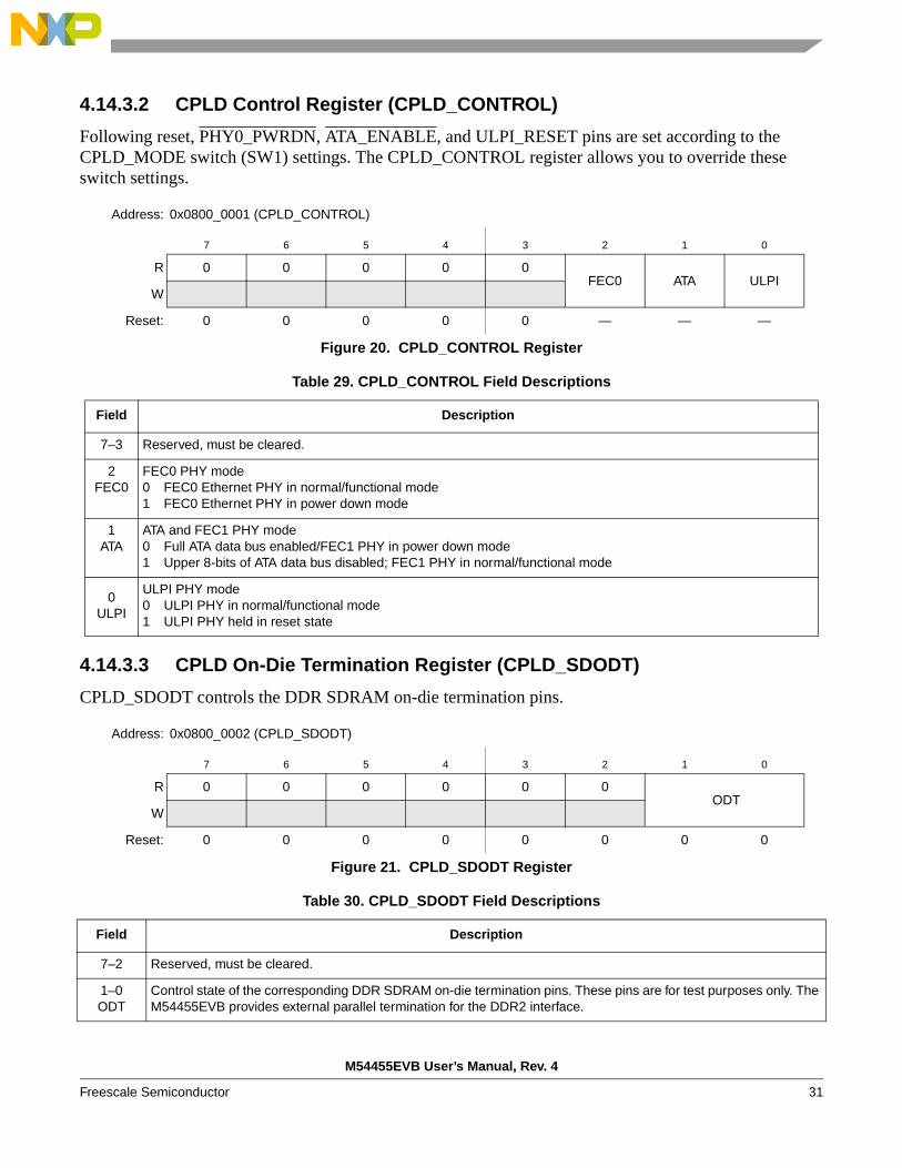
4.14.3.2 CPLD Control Register (CPLD_CONTROL)
Following reset, PHY0_PWRDN, ATA_ENABLE, and ULPI_RESET pins are set according to the CPLD_MODE switch (SW1) settings. The CPLD_CONTROL register allows you to override these switch settings.
4.14.3.3 CPLD On-Die Termination Register (CPLD_SDODT)
CPLD_SDODT controls the DDR SDRAM on-die termination pins.
Address: 0x0800_0001 (CPLD_CONTROL)
7 6 5 4 3 2 1 0
R 0 0 0 0 0FEC0 ATA ULPI
W
Reset: 0 0 0 0 0 — — —
Figure 20. CPLD_CONTROL Register
Table 29. CPLD_CONTROL Field Descriptions
Field Description
7–3 Reserved, must be cleared.
2FEC0
FEC0 PHY mode0 FEC0 Ethernet PHY in normal/functional mode1 FEC0 Ethernet PHY in power down mode
1ATA
ATA and FEC1 PHY mode0 Full ATA data bus enabled/FEC1 PHY in power down mode1 Upper 8-bits of ATA data bus disabled; FEC1 PHY in normal/functional mode
0ULPI
ULPI PHY mode0 ULPI PHY in normal/functional mode1 ULPI PHY held in reset state
Address: 0x0800_0002 (CPLD_SDODT)
7 6 5 4 3 2 1 0
R 0 0 0 0 0 0 ODT
W
Reset: 0 0 0 0 0 0 0 0
Figure 21. CPLD_SDODT Register
Table 30. CPLD_SDODT Field Descriptions
Field Description
7–2 Reserved, must be cleared.
1–0ODT
Control state of the corresponding DDR SDRAM on-die termination pins. These pins are for test purposes only. The M54455EVB provides external parallel termination for the DDR2 interface.
M54455EVB User’s Manual, Rev. 4
Freescale Semiconductor 31

4.14.3.4 CPLD Mode Register (CPLD_MODE)
CPLD_MODE reflects the current status of the SW1 switch.
4.14.3.5 CPLD Flash Configuration Register (CPLD_FLASHCFG)
CPLD_FLASHCFG controls the write-protect feature of Flash1
Address: 0x0800_0003 (CPLD_MODE)
7 6 5 4 3 2 1 0
RCPLD_MODE
W
Reset: 0 0 0 0 0 0 0 0
Figure 22. CPLD_MODE Register
Table 31. CPLD_MODE Field Descriptions
Field Description
7–0CPLD_MODE
Status of the CPLD_MODE[7:0] signals which are controllable via the SW1 switch.0 Corresponding SW1 switch is in the ON position1 Corresponding SW1 switch is in the OFF position
Address: 0x0800_0004 (CPLD_FLASHCFG)
7 6 5 4 3 2 1 0
R 0 0 0 0 0 0 0FLASH_WP
W
Reset: 0 0 0 0 0 0 0 1
Figure 23. CPLD_FLASHCFG Register
Table 32. CPLD_FLASHCFG Field Descriptions
Field Description
7–1 Reserved, must be cleared.
0FLASH_WP
Flash1 write-protect. This bit controls the state of the FLASH1_WP signal0 Flash1 is write-protected1 Flash1 is not write-protected
M54455EVB User’s Manual, Rev. 4
32 Freescale Semiconductor

4.14.3.6 CPLD LED Control Register (CPLD_LEDS)
CPLD_LEDS controls the state of the CPLD’s LEDs.
4.15 InterruptsThe four external MCF5445x interrupt requests are driven by the FPGA. The FPGA gathers four PCI interrupts from the PCI slots, along with two pushbutton interrupts, and presents them to the MCF5445x. Refer to Section 4.13, “FPGA” for details on how to enable and route the interrupts.
4.16 Serial Interface HeaderThe MCF5445x contains a few serial interfaces and timers that are not made available via dedicated interfaces on the M54455EVB. However, these interfaces (and others) are brought out to a general purpose header, J908, for easy access. The following interfaces are accessible on J908:
• DSPI• I2C• DMA external request/acknowledge• DMA timer input/output• UART0• UART1
Table 34 shows the signal assignments on J908.
Address: 0x0800_0005 (CPLD_LEDS)
7 6 5 4 3 2 1 0
R 0 0CPLD_LED
W
Reset: 0 0 0 0 0 0 0 0
Figure 24. CPLD_LEDS Register
Table 33. CPLD_LEDS Field Descriptions
Field Description
7–6 Reserved, must be cleared.
5–0CPLD_LED
Controls the state of the CPLD’s LED[5:0] signals. LED[5:0] corresponds to D35–D30. 0 Corresponding CPLD LED is OFF1 Corresponding CPLD LED is ON
M54455EVB User’s Manual, Rev. 4
Freescale Semiconductor 33

4.17 Serial PortsThe MCF5445x includes three UART modules. The M54455EVB provides two standard RS232 line drivers on UART0 and UART1, connected to a dual, stacked DB9 serial port connector (male). The RS232 null-modem cable provided in the kit can connect the serial ports to a host PC.
The EVB also supplies an optional USB-to-UART bridge (Silicon Labs CP2102) to interface with MCF5445x's UART0. If using this option, a USB type B connector can interface with a host PC instead of the standard RS232 connector. A custom virtual COMM port driver may be required on the host PC and can be found here:
http://www.silabs.com/tgwWebApp/public/web_content/products/Microcontrollers/USB/en/mcu_vcp.htm
Table 34. J908 Signal Assignments
Signal Name Pin Signal Name
VDD 1 2 GND
VDD 3 4 GND
U1CTS 5 6 U0TXD
U1RTS 7 8 U0RXD
U1RXD 9 10 U0RTS
U1TXD 11 12 U0CTS
GND 13 14 GND
SYSRESET 15 16 I2C_SCL
CPU_RSTOUT 17 18 I2C_SDA
GND 19 20 GND
T3IN 21 22 IRQ7
T2IN 23 24 IRQ4
T1IN 25 26 IRQ3
T0IN 27 28 IRQ1
GND 29 30 GND
DSPI_SCK 31 32 DSPI_PCS0
DSPI_SIN 33 34 DSPI_PCS1
DSPI_SOUT 35 36 DSPI_PCS2
DSPI_PCS5 37 38 DACK0
GND 39 40 DREQ0
M54455EVB User’s Manual, Rev. 4
34 Freescale Semiconductor

NOTEThe virtual COMM port driver loses communication with the M54455EVB when the board is powered off and back on. You must force a reconnect in the serial terminal program following a power-on reset of the EVB. For this reason, it can be difficult to see power-on boot messages from the EVB when using the power button on the front of the M54455EVB’s case. However, the EVB provides a reset button (SW2) which does not force the CP2102 to re-enumerate, and thus, does not require a reconnect in the serial terminal. This allows you to witness any reset messages, but requires that the case be opened so that SW2 can be accessed.
4.18 Logic Analyzer ConnectionsThe M54455EVB provides 12 Tektronix P6860 compression connections for use with TLA7Axx logic analyzer modules. These probes allow you to probe Flexbus, PCI and DDR2 signals. See the M54455EVB schematics for more details.
4.19 Power RegulationThe M54455EVB provides two Freescale QuiccSupply MC34702 power regulators. These power regulators provide 3.3 V, 1.8 V, 1.5 V, and 1.2 V to devices on the board, with the exception of the PCI slots. The regulators generate these voltages from a 5-V external supply. The 5-V supply can be provided through one of the following: the ATX power connector, a barrel jack connector, or a 6-pin molex power connector to a lab-grade regulated supply.
Jumpers are provided that allow for the 3.3- and 1.5-V supplies to be separated from the MCF5445x. The intention of these jumpers is to connect a current meter to measure the power consumed by the MCF5445x processor or to allow for the injection of a variable voltage power supply for test purposes.
The PCI sockets are powered directly from the ATX supply, which allows for much higher PCI card power consumption. PCI is only available if an ATX supply powers the board. The ATX 5-V line is connected to the Freescale QuiccSupply MC34702 regulators. This isolates the power consumption of the PCI bus from the board ASICs.
4.20 Jumpers, Headers, and SwitchesThere are several jumpers on the M54455EVB that allow you to control the hardware configuration. The following table provides descriptions for all the jumper settings.
Table 35. Jumper Settings
Reference Designator Setting1 Function
H4[1:2]ON
Clock Generator DisableOFF2
H4[3:4]ON 33MHz PCICLK/CLKIN Frequency
OFF2 66MHz PCICLK/CLKIN Frequency
M54455EVB User’s Manual, Rev. 4
Freescale Semiconductor 35

The following table describes the interface headers.
H10ON2
Power Barrel Connector EnableOFF
H11
ON Enable VDD to the processor
OFF2 Disable VDD to the processorNote: R665 is fitted by default and bypasses H11
H12
ON Enable VEE to the processor
OFF2 Disable VEE to the processorNote: R664 is fitted by default and bypasses H12
H13
ON Enable V1.5 to the processor
OFF2 Disable V1.5 to the processorNote: R659 is fitted by default and bypasses H13
H21[1:2]H21[3:4]H21[5:6]H21[7:8]
ONConnect I2C_SCL, I2C_SDA, ATA_BUFFER_EN, and DSPI_PCS2 from MCF5445x to FPGA program header pinsOFF2
JP907JP908
ON2 Enable UART1 flow control signals
OFF Disable UART1 flow control signals
JP9031:2 Boot into JTAG mode
2:32 Boot into BDM mode
JP9041:22 Connect BDM pin 24 to MCF5445x TCLK_PSTCLK
2:3 Connect BDM pin 6 to MCF5445x TCLK_PSTCLK
JP909JP910JP911JP912
1:2 Connect UART0 signals to DB9 interface
2:32 Connect UART0 signals to USB interface
JP9181:22 Connect MCF5445x USBCLKIN to CLKOUT of USB3300
2:3 Connect MCF5445x USBCLKIN to 60MHz from external clock generator
1 ON indicates that a shunt should be fitted on the jumper; OFF indicates that no shunt should be applied.2 Default setting.
Table 36. Interface Headers
Reference Designator Function
H9 System power indicator for case LED
H14 Board reset header for case switch
H15 Power ON/OFF for case switch
H16 ATA activity indicator for case LED
H20 FPGA program header
Table 35. Jumper Settings (continued)
Reference Designator Setting1 Function
M54455EVB User’s Manual, Rev. 4
36 Freescale Semiconductor
The following table provides a description of the various switches on the board.
5 U-BootThe M54455EVB comes pre-programmed with the U-Boot bootloader in the boot flash device, Flash0. U-Boot is an open source bootloader with some debugging capabilities. Please refer to http://www.denx.de/wiki/UBoot for documentation.
6 Revision History
H26 CPLD program header
H36Alternate 12V supply for PCI cards.Default uses the ATX power supply (J50)
H900 Spare CPLD I/O pins
J21Alternate power connector.Default uses the ATX power supply (J50)
J24 BDM/JTAG connector
J909 Serial interface breakout
J910 SSI interface signals
Table 37. Switches
Reference Designator Function
SW1CPLD_MODE switch.See Section 4.14, “CPLD” for more information.
SW2 Board reset push-button
SW3Parallel configuration switch.See Section 4.3, “MCF5445x Boot Options” for details.
SW4 ATX power ON/OFF button.
SW5 FPGA_CFG switch. Not used at this time
SW6 FPGA interrupt pushbutton 0.
SW7 FPGA interrupt pushbutton 1.
Table 38. M54455EVBUM Revision History
Revision Release Date Changes
3 30 Aug 2007 Initial revision for public launch
4 30 Jan 2008Changed step 8 in Installation and Configuration section from “bootm” to “bootm 0”
Table 36. Interface Headers (continued)
Reference Designator Function
M54455EVB User’s Manual, Rev. 4
Freescale Semiconductor 37

Document Number: M54455EVBUMRev. 401/2008
How to Reach Us:
Home Page:www.freescale.com
Web Support:http://www.freescale.com/support
USA/Europe or Locations Not Listed:Freescale Semiconductor, Inc.Technical Information Center, EL5162100 East Elliot RoadTempe, Arizona 85284+1-800-521-6274 or +1-480-768-2130www.freescale.com/support
Europe, Middle East, and Africa:Freescale Halbleiter Deutschland GmbHTechnical Information CenterSchatzbogen 781829 Muenchen, Germany+44 1296 380 456 (English)+46 8 52200080 (English)+49 89 92103 559 (German)+33 1 69 35 48 48 (French)www.freescale.com/support
Japan:Freescale Semiconductor Japan Ltd.HeadquartersARCO Tower 15F1-8-1, Shimo-Meguro, Meguro-ku,Tokyo 153-0064Japan0120 191014 or +81 3 5437 [email protected]
Asia/Pacific:Freescale Semiconductor Hong Kong Ltd.Technical Information Center2 Dai King StreetTai Po Industrial EstateTai Po, N.T., Hong Kong+800 2666 [email protected]
For Literature Requests Only:Freescale Semiconductor Literature Distribution CenterP.O. Box 5405Denver, Colorado 802171-800-441-2447 or 303-675-2140Fax: [email protected]
Information in this document is provided solely to enable system and software implementers to use Freescale Semiconductor products. There are no express or implied copyright licenses granted hereunder to design or fabricate any integrated circuits or integrated circuits based on the information in this document.
Freescale Semiconductor reserves the right to make changes without further notice to any products herein. Freescale Semiconductor makes no warranty, representation or guarantee regarding the suitability of its products for any particular purpose, nor does Freescale Semiconductor assume any liability arising out of the application or use of any product or circuit, and specifically disclaims any and all liability, including without limitation consequential or incidental damages. “Typical” parameters that may be provided in Freescale Semiconductor data sheets and/or specifications can and do vary in different applications and actual performance may vary over time. All operating parameters, including “Typicals”, must be validated for each customer application by customer’s technical experts. Freescale Semiconductor does not convey any license under its patent rights nor the rights of others. Freescale Semiconductor products are not designed, intended, or authorized for use as components in systems intended for surgical implant into the body, or other applications intended to support or sustain life, or for any other application in which the failure of the Freescale Semiconductor product could create a situation where personal injury or death may occur. Should Buyer purchase or use Freescale Semiconductor products for any such unintended or unauthorized application, Buyer shall indemnify and hold Freescale Semiconductor and its officers, employees, subsidiaries, affiliates, and distributors harmless against all claims, costs, damages, and expenses, and reasonable attorney fees arising out of, directly or indirectly, any claim of personal injury or death associated with such unintended or unauthorized use, even if such claim alleges that Freescale Semiconductor was negligent regarding the design or manufacture of the part.
RoHS-compliant and/or Pb-free versions of Freescale products have the functionality and electrical characteristics as their non-RoHS-compliant and/or non-Pb-free counterparts. For further information, see http://www.freescale.com or contact your Freescale sales representative.
For information on Freescale’s Environmental Products program, go to http://www.freescale.com/epp.
Freescale™ and the Freescale logo are trademarks of Freescale Semiconductor, Inc. All other product or service names are the property of their respective owners.© Freescale Semiconductor, Inc. 2008. All rights reserved.