M14A2A User Manual - fccid.io · M14A2A User Manual ... 9.5 dBi in 1900 MHz Band Assuming...
28
1 / 28 □ Normal □ Internal Use Confidential □ Re stricted Confidential M14A2A User Manual Project Name: M14A2A Author: Wistron NeWeb Corporation Revision: 1.0 Revision Date: 2016/04/06
Transcript of M14A2A User Manual - fccid.io · M14A2A User Manual ... 9.5 dBi in 1900 MHz Band Assuming...

1 / 28 Normal Internal Use Confidential Restricted Confidential
M14A2A User Manual
Project Name: M14A2A
Author: Wistron NeWeb Corporation
Revision: 1.0
Revision Date: 2016/04/06
2 / 28 Normal Internal Use Confidential Restricted Confidential
M14A2A User Manual
Contact Information
Sale and Technical Support [email protected]
Website www.wnc.com.tw

3 / 28 Normal Internal Use Confidential Restricted Confidential
M14A2A User Manual
© Wistron NeWeb Corporation
THIS DOCUMENT AND THE INFORMATION CONTAINED HEREIN IS PROPRIETARY AND IS THE EXCLUSIVE
PROPERTY OF WNC AND SHALL NOT BE DISTRIBUTED, REPRODUCED, OR DISCLOSED IN WHOLE OR IN
PART WITHOUT PRIOR WRITTEN PERMISSION FROM WNC.
LIMITATION OF LIABILITY
THIS DOCUMENT AND THE INFORMATION CONTAINED HEREIN IS PURELY FOR DESIGN REFERENCE AND
SUBJECT TO REVISION BY WNC AT ANY TIME. NOTHING IN THIS DOCUMENT SHALL BE CONSTRUED AS
GRANTING ANY WARRANTY OR RIGHT TO USE THE MATERIAL CONTAINED HEREIN WITHOUT WNC’S
PRIOR EXPRESS WRITTEN CONSENT. WNC SHALL NOT BE LIABLE FOR ANY USE, APPLICATION OR
DEVELOPMENT DERIVED FROM THE MATERIAL WITHOUT SUCH PRIOR EXPRESS WRITTEN CONSENT.
Federal Communication Commission Interference Statement
This device complies with Part 15 of the FCC Rules. Operation is subject to the following two conditions:
(1) This device may not cause harmful interference, and (2) this device must accept any interference
received, including interference that may cause undesired operation.
This equipment has been tested and found to comply with the limits for a Class B digital device, pursuant
to Part 15 of the FCC Rules. These limits are designed to provide reasonable protection against harmful
interference in a residential installation. This equipment generates, uses and can radiate radio frequency
energy and, if not installed and used in accordance with the instructions, may cause harmful
interference to radio communications. However, there is no guarantee that interference will not occur
in a particular installation. If this equipment does cause harmful interference to radio or television
reception, which can be determined by turning the equipment off and on, the user is encouraged to try
to correct the interference by one of the following measures:
- Reorient or relocate the receiving antenna.
- Increase the separation between the equipment and receiver.
- Connect the equipment into an outlet on a circuit different from that to which the receiver is
connected.
- Consult the dealer or an experienced radio/TV technician for help.
Any changes or modifications not expressly approved by the party responsible for compliance could void
the user's authority to operate this equipment. This transmitter must not be co-located or operating in
conjunction with any other antenna or transmitter.
Radiation Exposure Statement
This equipment complies with FCC radiation exposure limits set forth for an uncontrolled environment.
This equipment should be installed and operated with minimum distance 20 cm between the radiator &
your body.

4 / 28 Normal Internal Use Confidential Restricted Confidential
M14A2A User Manual
This device is intended only for OEM integrators under the following conditions:
(1) The antenna must be installed such that 20 cm is maintained between the antenna and use rs,
(2) The transmitter module may not be co-located with any other transmitter or antenna.
(3) To comply with FCC regulations limiting both maximum RF output power and human exposure to RF
radiation, the maximum antenna gain including cable loss in a mobile exposure condition must not
exceed:
Standalone Condition:
。 10.1 dBi in 700 MHz Band
。 6.5 dBi in 1700 MHz Band
。 9.5 dBi in 1900 MHz Band
Assuming collocated with a WLAN transmitter with maximum 34 dBm average EIRP power
。 7.0 dBi in 700 MHz Band
。 6.5 dBi in 1700 MHz Band
。 9.5 dBi in 1900 MHz Band
Remark: This assumption is not valid if the output power of the collocated WLAN transmitter is higher
than 34 dBm.

5 / 28 Normal Internal Use Confidential Restricted Confidential
M14A2A User Manual
Contents
Contact Information ........................................................................................................................... 2
Contents ............................................................................................................................................ 5
1. Introduction…………………………………………………………………………………………………………………………….…7
1.1. Features........................................................................................................................... 7
2. Electrical Specifications .............................................................................................................. 8
2.1. Interface pin assignments................................................................................................. 8
2.1.1. LGA Pad Diagram .................................................................................................. 8
2.1.2. Pin Assignments.................................................................................................... 9
2.2. Power supply ................................................................................................................. 10
2.3. USB interface ................................................................................................................. 10
2.4. SIM interface ................................................................................................................. 11
2.5. Control interface (signals)............................................................................................... 12
2.5.1. Power-on Signal .................................................................................................. 12
2.5.2. Host-to-modem wake-up interface ...................................................................... 13
2.5.3. Reset Signal ........................................................................................................ 14
2.6. Digital interface.............................................................................................................. 15
2.6.1. PCM Interface ..................................................................................................... 15
2.6.2. I2S Interface ....................................................................................................... 15
2.6.3. I2C Interface ....................................................................................................... 16
2.6.4. UART Interface.................................................................................................... 16
2.7. ADC interface ................................................................................................................. 17
2.8. GPIO .............................................................................................................................. 17
3. RF Specifications ...................................................................................................................... 18
3.1. RF connections............................................................................................................... 18
3.2. Interference and sensitivity ............................................................................................ 18
3.3. Radiated sensitivity measurement .................................................................................. 19
3.4. Supported frequencies ................................................................................................... 19
4. Power ...................................................................................................................................... 20
4.1. Module power states ..................................................................................................... 20
5. Software Interface ................................................................................................................... 22
6. Mechanical and Environmental Specifications.......................................................................... 23
6.1. PCBA form factor............................................................................................................ 23
6 / 28 Normal Internal Use Confidential Restricted Confidential
M14A2A User Manual
6.2. Labeling ......................................................................................................................... 25
6.3. Thermal considerations .................................................................................................. 25
7. Regulatory and Industry Approvals .......................................................................................... 26
7.1. Certification testing........................................................................................................ 26
7.2. Safety and hazards ......................................................................................................... 26
8. References ............................................................................................................................... 27
8.1. Web site support............................................................................................................ 27
8.2. WNC documents ............................................................................................................ 27
9. Safety Recommendation .......................................................................................................... 28

7 / 28 Normal Internal Use Confidential Restricted Confidential
M14A2A User Manual
1. Introduction
M14A2A is a Cat. 1 (10 Mbps/5 Mbps DL/UL respectively) LTE modem which incorporates an application
CPU subsystem and a host of peripheral interfaces and functions uniquely designed to address the
power/performance/cost requirements of IoT and M2M applications. The chip is based on SDR-v3.0
(Software Defined Radio) architecture which offers OFDMA-related software based signal processing
capabilities that significantly exceed traditional communications DSP cores, yet consumes a fraction of
the power.
The CPU su syste features a high perfor a e MIP“ Mi roAptiv™ pro essor running a Linux OS with a
variety of host interfaces including USB 2.0, I2C, SPI, and UART. The module supports integrated VoLTE
functionality with a variety of narrow and wide-band CODECs and full IMS signaling.
1.1. Features
3GPP category support: LTE CAT-1 with 10/5 Mbps for DL/UL
Embedded 512Mbit LPDDR
Embedded 256Mbit SPI NOR Flash
Ultra-high performance enhanced SDR processor
Embedded network processor with Linux OS
Integrated support for VoLTE including HD voice
Integrated PMU circuitry
Integrated RTC support
I terfere e Ca ellatio INCA™ apa ility
Optimized for the M2M and IoT markets
Interfaces:
– HS USB2.0 with integrated PHY
– Dual UART interfaces (4 bit and 2 bit) for high-speed data transfer and diagnostic tools
support
– SPI master interface
– Mobile LPDDR and PSRAM support
– Serial NOR flash controller
– USIM interface
– I2S/PCM audio interface
– GPIOs
– One I2C interface

8 / 28 Normal Internal Use Confidential Restricted Confidential
M14A2A User Manual
2. Electrical Specifications
2.1. Interface pin assignments
2.1.1. LGA Pad Diagram
Figure 1. LGA pad diagram (top view)

9 / 28 Normal Internal Use Confidential Restricted Confidential
M14A2A User Manual
2.1.2. Pin Assignments
I/O type description :
AO : Analog Output
AI : Analog Input
DO : Digital Output
DI : Digital Input
Table 1. Pin Interface Family
Interface Family Signal Name Description I/O
RF Interfaces RF_1 Main Antenna AI/AO
RF_2 Aux Antenna AI
User Identity Module
UIM_VCC UIM Power DO
UIM_DATA UIM Data in/out DI/DO
UIM_CLK UIM Clock DO
UIM_RESET UIM Reset DO
UIM_DETECT UIM Detect DI/DO
Data Interfaces
USB2.0 USB_Dp USB Data Positive DI/DO
USB_Dn USB Data Negative DI/DO
UART1
UART1_CTS Clear To Send for UART 1 DI
UART1_RTS Request To Send for UART 1 DO
UART1_RX Receive for UART 1 DI
UART1_TX Transmit for UART 1 DO
UART2 UART2_RX Receive for UART2 DI
UART2_TX Transmit for UART2 DO
I2C I2C_SDA I2C Data DI/DO
I2C_SCL I2C Clock DI/DO
SPI
SPIM_MOSI SPI Master Out Slave In DO
SPIM_MISO SPI Master In Slave Out DI
SPIM_EN SPI master interface enable DO
SPIM_CLK SPI master interface clock DO
Module Control and State Interfaces
WWAN_STATE Wireless WAN Radio State DI
POWER_ON Power On the module DO
WAKEUP_OUT Module wakes up host OR GPIO DI
WAKEUP_IN Host wakes up module OR GPIO. DI
RESET Reset the module AI
Power and GND
VREF Reference Logic Voltage AI
VCC Main Power AO
GND Ground AI
General Purpose GPIO General Purpose I/O DI/DO
ADC Analog to Digital Convertor AI
Audio PCM/I2S
PCM_SYNC PCM_SYNC DI /DO
PCM_IN PCM_IN DI
PCM_OUT PCM_OUT DO
PCM_CLK PCM_CLK DO

10 / 28 Normal Internal Use Confidential Restricted Confidential
M14A2A User Manual
2.2. Power supply
M14A2A includes an integrated Power Manager enabling single and direct voltage supply from the
battery and reducing the overall bill of materials.
Table 2. Power supply specifications
Power Signal Name Pin No. Description Voltage Levels (V)
Min. Typ. Max.
VCC VCC1 to VCC6 37–42 Main Power Supply 3.3 3.8 4.2
2.3. USB interface
M14A2A complies with USB 2.0 high-speed protocol. The USB input/output lines comply with USB 2.0
specifications.
Table 3. Signals of the USB interface
Name Description Input/Output
(Direction to module)
Voltage Levels (V)
Min. Typ. Max.
D+
USB data positive
(low-/full-speed)
Input High 2 3.3 3.6
Input Low 0 – 0.8
Output High 2.8 3.3 3.6
Output Low – – 0.3
USB data positive
(high-speed)
Input High 0.3 – 0.44
Input Low 0 – 0.01
Output High 0.36 0.38 0.44
Output Low 0 – 0.01
D–
USB data negative
(low-/full-speed)
Input High 2 3.3 3.6
Input Low 0 – 0.8
Output High 2.8 3.3 3.6
Output Low – – 0.3
USB data negative
(high-speed)
Input High 0.3 – 0.44
Input Low 0 – 0.01
Output High 0.36 0.38 0.44
Output Low 0 – 0.01
Layout suggestion:
Differential impedance: 90 Ω
Space to other signals should be at least 20 mils
Intra-pair length mismatch should be less than 150 mils
USB Length in M14A2A is tuned as below:

11 / 28 Normal Internal Use Confidential Restricted Confidential
M14A2A User Manual
2.4. SIM interface
M14A2A includes an SC controller, interface pins, and a dedicated LDO (3.0 V or 1.8 V).
Since M14A2A is not equipped with a SIM socket, it must place a SIM socket on the user interface board.
M14A2A provides a UIM_DETECT input pin to detect if the SIM card is present. If the USIM card is
present, UIM_DETECT should be high. (The voltage level should be 1.8 V) If the USIM card is absent,
UIM_DETECT should be low. (The module is internally pulled down.) It was recommended to choose a
SIM socket with the Card Detect pin. If the SIM card is preset, the pin will not contact the ground and
pull up to 1.8 V through a 2 kΩ resistor. If the SIM card is absent, the pin will normally contact the ground.
Other types of SIM sockets which can achieve this feature are also acceptable.
A 100 nF capacitor and a 1 μF apa itor are placed between the UIM_VCC and Ground pins in a parallel
manner. (If the UIM_VCC circuit is too long, a larger capacitor such as a 4.7 μF capacitor can be
employed if necessary.) Four 33 pF capacitors (0402 package is recommended.) are placed between the
UIM_VCC and Ground pins, the UIM_CLK and Ground pins, the UIM_DATA and Ground pins, and the
UIM_RESET and Ground pins in parallel to filter out interference from RF signals. (An R/C circuit on pin
UIM_CLK is optional. If there is an EMI issue on this clock signal, try to adjust these R/C values.)
We recommend taking protective measures against electrostatic discharge (ESD) near the SIM socket.
The TVS diode with a VRWM of 5 V and junction capacitance of less than 10 pF must be placed as close as
possible to the SIM socket, and the Ground pin of the ESD protection component must be well
connected to the power Ground pin that supplies power to M14A2A.
Figure 2. SIM card interface circuit

12 / 28 Normal Internal Use Confidential Restricted Confidential
M14A2A User Manual
2.5. Control interface (signals)
This section describes the host-to-modem wake-up interface and power-on signal to enable or disable
the control module.
2.5.1. Power-on Signal
The POWER_ON pad is an input signal used to control whether the module is in the Module Enabled or
Module Disabled state. Do not toggle the PERST# pin during power-on. This signal has the highest
priority over the wakeup, the alarms signals, and the digital control pins.
The POWER_ON signal is Active Low (VIL for VREF), its voltage level is 1.8V if going to High for Module
Disabled:
POWER_ON is High: Module is OFF
POWER_ON is Low: Module is ON
There are three possible states of the module:
Module Off - VCC is not present.
Module Enabled - VCC is supplied, and the module is enabled.
Module Disabled - VCC is supplied, and the module is disabled.
The state transitions are defined as follows:
When voltage is applied to VCC, the module shall enter the Module Disabled state.
An input to the POWER_ON pad shall trigger the transition from the Module Disabled to the
Module Enabled state.
An input to the POWER_ON pad shall trigger the transition from the Module Enabled to the
Module Disabled state.
Figure 3. Power ON/OFF timming
In order to prevent the POWER_ON signal in a floating state, it was recommended to pull LOW for
Module Enabled, or pull HIGH to VREF for Module Disabled.

13 / 28 Normal Internal Use Confidential Restricted Confidential
M14A2A User Manual
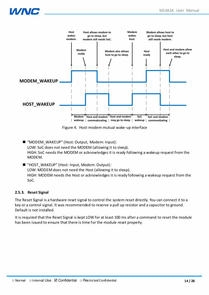
2.5.2. Host-to-modem wake-up interface
In applications where the device power consumption is a major target of optimization such as
battery-operated sensors that are based on IOT/M2M modem solution and in addition, include a
third-party host, it is necessary to define a simple interface that will allow both the modem and the host
to be able to enter low power states whenever possible while allowing the other side to wake it up when
required.
For example, if the host has no data to transmit or any other tasks, it may wish to enter some low power
state according to its own capabilities and configurations. If during the time the host is in a low power
state and the modem suddenly receives data, it must wake-up the host.
A similar requirement exists from the other side. If, for example, the modem is in a low power state and
suddenly the host must transmit data, it must to be able to wake-up the modem.
Each side has notification functionality when they are up and ready to follow a wake-up request.
The idea behind the suggested method is to have a very simple interface that will also be pin-limited
(requires only two pins) to fit into such limited-pin-count applications and packages.
The interface consists of two lines: one is driven by the host and received by the modem, and the other
is driven by the modem and received by the host.
Each side can wake the other side by toggling it high and allowing the other side to go to sleep when not
needed by toggling it low.
Toggling the signal high does not necessary mean the other side will enter the low power state; the
toggling function is only intended to notify the other side that its functions will not be required in the
near term and that it is allowed to enter a low power state if he can (according to its own tasks,
configurations, and capabilities).
The following diagram depicts how this simple interface works. In addition to the two hardware signals,
additional higher-level messages may be defined to pass further information or details between the host
and the modem if required.
If the Powe states of Deep “leep a d Light Hibe atio featu e a e e ui ed, it was eco e ded to connect WAKEUP_IN and WAKEUP_OUT signal to Host. This design can make sure M14A2A can be
waked up by Host.
14 / 28 Normal Internal Use Confidential Restricted Confidential
M14A2A User Manual
MODEM_WAKEUP
HOST_WAKEUP
Modem
wakeupHost and modem
communicating
Host and modem
may go to sleep
SoC
wakeupSoC and modem
communicating
Host
wakes
modem.
Modem
ready
Host allows modem to
go to sleep, but
modem still needs SoC.
Modem also allows
host to go to sleep.
Modem
wakes
host.
Host
ready
Modem allows host to
go to sleep, but host
still needs modem.
Host and modem allow
each other to go to
sleep.
Figure 4. Host-modem mutual wake-up interface
MODEM_WAKEUP Host: Output, Modem: Input):
LOW: SoC does not need the MODEM (allowing it to sleep).
HIGH: SoC needs the MODEM or acknowledges it is ready following a wakeup request from the
MODEM.
HO“T_WAKEUP Host: I put, Mode : Output :
LOW: MODEM does not need the Host (allowing it to sleep).
HIGH: MODEM needs the Host or acknowledges it is ready following a wakeup request from the
SoC.
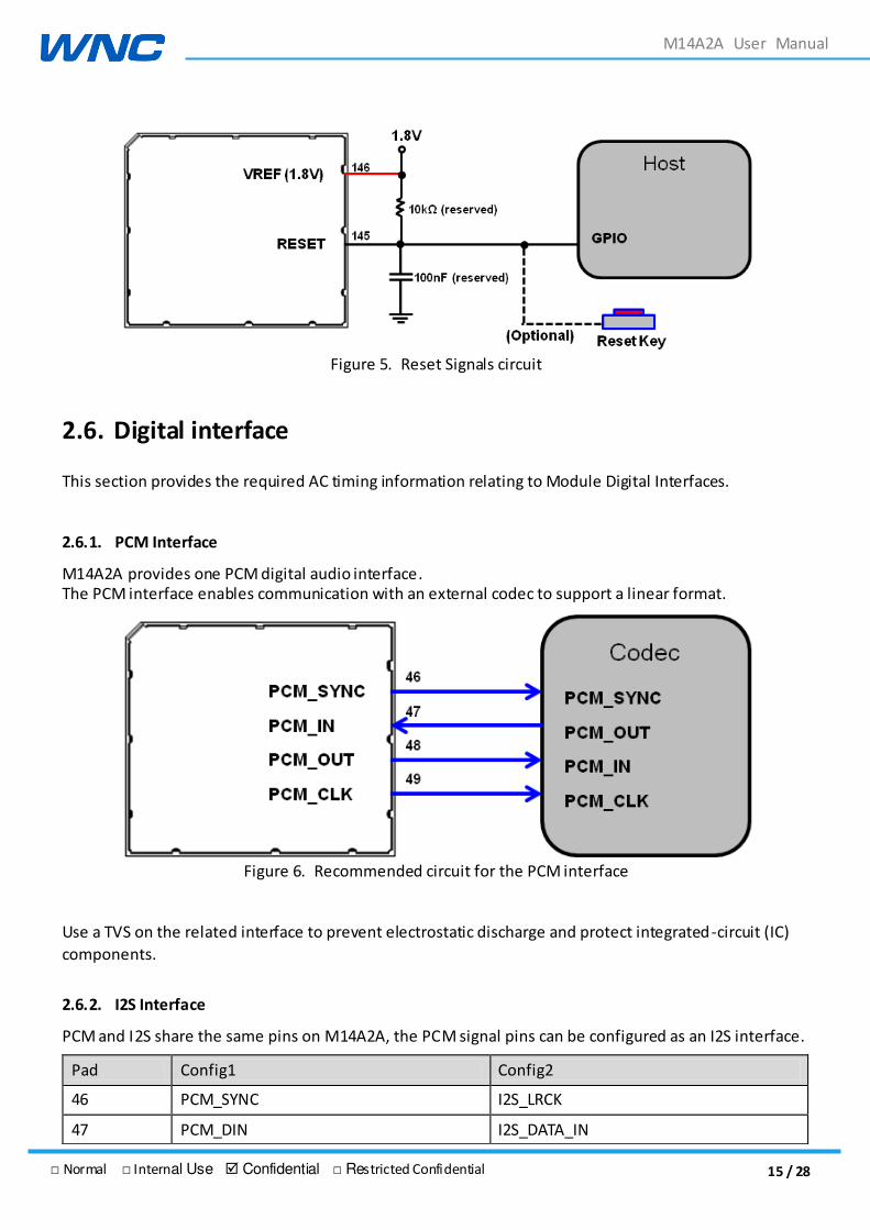
2.5.3. Reset Signal
The Reset Signal is a hardware reset signal to control the system reset directly. You can connect it to a
key or a control signal. It was recommended to reserve a pull up resistor and a capacitor to ground.
Default is not installed.
It is required that the Reset Signal is kept LOW for at least 100 ms after a command to reset the module
has been issued to ensure that there is time for the module reset properly.
15 / 28 Normal Internal Use Confidential Restricted Confidential
M14A2A User Manual
Figure 5. Reset Signals circuit
2.6. Digital interface
This section provides the required AC timing information relating to Module Digital Interfaces.
2.6.1. PCM Interface
M14A2A provides o e PCM digital audio i terfa e The PCM interface enables communication with an external codec to support a linear format.
Figure 6. Recommended circuit for the PCM interface
Use a TVS on the related interface to prevent electrostatic discharge and protect integrated-circuit (IC)
components.
2.6.2. I2S Interface
PCM and I2S share the same pins on M14A2A, the PCM signal pins can be configured as an I2S interface.
Pad Config1 Config2
46 PCM_SYNC I2S_LRCK
47 PCM_DIN I2S_DATA_IN

16 / 28 Normal Internal Use Confidential Restricted Confidential
M14A2A User Manual
Figure 7. Recommended circuit for the I2S interface
2.6.3. I2C Interface
There is one I2C interface in M14A2A. It was recommended to add pull high to 1.8 V through resistors
with values of 2.2 kΩ to 4.7 kΩ. ICs and sensors can use the same I2C interface. M14A2A can recognize
them by different addresses.
Figure 8. Recommended circuit for the I2C interface
2.6.4. UART Interface
There are dual UART interfaces. One is 4 bit for high-speed data transfer, and the other is 2 bit for
diagnostic tools and debugging.
48 PCM_DOUT I2S_DATA_OUT
49 PCM_CLK I2S_BCK

17 / 28 Normal Internal Use Confidential Restricted Confidential
M14A2A User Manual
2.7. ADC interface
One Analog to Digital Converter (ADC) input is provided by M14A2A. The converter is of a 10 bit
resolution, ranging from 0 V to 1.95 V with a sampling rate of 2 MHz. They can be used for customer
applications.
Table 4. ADC interface
Signal Name Pads Type Description
ADC 122 Analog Analog to digital conversion input
2.8. GPIO
M14A2A includes general purpose I/O signals that are summarized in the following table. These GPIOs
are available for customer-defined purposes such as control, signaling, and monitoring. Some GPIO
signals also can be configured as PCM signals for audio applications.
Table 5. GPIOs
Signal Name Pads Description Alt. Function
GPIO01 52 Configurable general purpose I/O
GPIO02 53 Configurable general purpose I/O
GPIO03 54 Configurable general purpose I/O
GPIO04 55 Configurable general purpose I/O
GPIO05 129 Configurable general purpose I/O
GPIO06 130 Configurable general purpose I/O
GPIO07 131 Configurable general purpose I/O
GPIO08 132 Configurable general purpose I/O
GPIO46 46 Configurable general purpose I/O PCM_SYNC
GPIO47 47 Configurable general purpose I/O PCM_IN
GPIO48 48 Configurable general purpose I/O PCM_OUT
GPIO49 49 Configurable general purpose I/O PCM_CLK
GPIO87 87 Configurable general purpose I/O
GPIO93 93 Configurable general purpose I/O
GPIO94 94 Configurable general purpose I/O
GPIO95 95 Configurable general purpose I/O
GPIO96 96 Configurable general purpose I/O
GPIO97 97 Configurable general purpose I/O

18 / 28 Normal Internal Use Confidential Restricted Confidential
M14A2A User Manual
3. RF Specifications
3.1. RF connections
M14A2A provides two RF pads; developers can connect them via 50 Ω traces to the main board.
TRX pads – RX/TX path
DRX pads – Diversity path
It is recommended to have keep-out under the two RF pads.
3.2. Interference and sensitivity
This section is to help developers to identify the interference that may affect M14A2A when adopting it
in systems.
Interference from other wireless devices
Harmonics or inter-modulated signals generated from wireless devices that fall in RX ranges of M14A2A
may result in degraded RX performance.
It is highly recommended to check the RX performance of the entire systems in the shielding
environment.
Interference from the host interface
High-speed switching signal elements in the system can easily couple noise to the module
(Ex.: DDR memory, LCD modules, DC-DC converter).
Methods to avoid sources of interference
Antenna location is important; it is recommended that the antenna away from high-speed switching
signals. Tracing from the module to the antenna is recommended to be as short as possible and must be
shielded by complete grounding.
However, M14A2A is well-shielded. The high-speed elements in the system are recommend to be
reserved for shielding during an early stage of a proje t’s develop e t.

19 / 28 Normal Internal Use Confidential Restricted Confidential
M14A2A User Manual
3.3. Radiated sensitivity measurement
Over-the-air testing can demonstrate the TRX ability of the whole system. Keys elements that affect the
measurement are:
Module ability (refer Specification)
Antenna Gain
System noise source
The OTA performance should be performed in an OTA chamber.
3.4. Supported frequencies
Table 6. M14A2A supported frequencies
Band Uplink (MHz) Downlink (MHz)
LTE Band 2 1,850–1,910 1,930–1,990
LTE Band 4 1,710–1,755 2,110–2,155
LTE Band 12 699–716 729–746
Table 7.
Band
Bandwidth
1.4 MHz 3 MHz 5 MHz 10 MHz 15 MHz 20 MHz
LTE Band 2
V V V V
LTE Band 4
V V V V
LTE Band 12
V V
Table 8. Conducted Tx power
Band Items Parameter Unit Min. Typ. Max.
LTE Band 2 Max TX Power 10 MHz 12RBs/QPSK dBm 21.5 22.5 23.5
LTE Band 4 Max TX Power 10 MHz 12RBs/QPSK dBm 21.5 22.5 23.5
LTE Band 12 Max TX Power 10 MHz 12RBs/QPSK dBm 21.5 22.5 23.5
Table 9. Conducted Rx sensitivity
Band Items Parameter Unit Min. Typ. Max.
LTE Band 2 Receive Sensitivity 10 MHz with 50 RBs dBm –96.3 –94.3
LTE Band 4 Receive Sensitivity 10 MHz with 50 RBs dBm –98.3 –96.3
LTE Band 12 Receive Sensitivity 10 MHz with 50 RBs dBm –95.3 –93.3

20 / 28 Normal Internal Use Confidential Restricted Confidential
M14A2A User Manual
4. Power
4.1. Module power states
In the operational modes, the system can be configured to use the different power states .
The system state is selected according to the permissions, required activity, and the available expected
time until the next power state.
This method allows the power management to be very dynamic and flexible and to be tuned according
to the needs of each product/application and according to specific conditions.
The following table shows several main system operational modes and the different system power states
used in each mode.
If the Power states of Deep Sleep and Light Hibernation feature are required, it was recommended
to connect WAKEUP_IN and WAKEUP_OUT signal to Host. This design can make sure M14A2A can be
waked up by Host.
Table 10. System operational modes
System Operational Mode System Power State Description
Idle Registered (short
paging interval)
Active Wake up
Active The modem is currently listening to the channel,
decoding paging message etc
Deep sleep The modem is in deep sleep; modem state info is
fully retained on the baseband side.
Idle Registered (short
paging interval)
Active Wake up
Active The modem is listening for paging.
Light Hibernation The modem state is retained in the DDR and
reconstructed when returning to active.
Idle Registered (long
paging cycle) or PSM
Active Wake up
Active The modem is currently listening to the channel,
decoding paging message etc.
Off
The modem stores its state info on the host, flash
memory, or other non-volatile memory. The
modem internal memory and DDR data are not
stored and are completely shut down.
Connected Active All different active modes
Connected long-DRX Deep sleep
Connected short-DRX Light sleep
Detached Active The modem performs scanning for networks.
Shutdown Off The modem is shut down.
21 / 28 Normal Internal Use Confidential Restricted Confidential
M14A2A User Manual
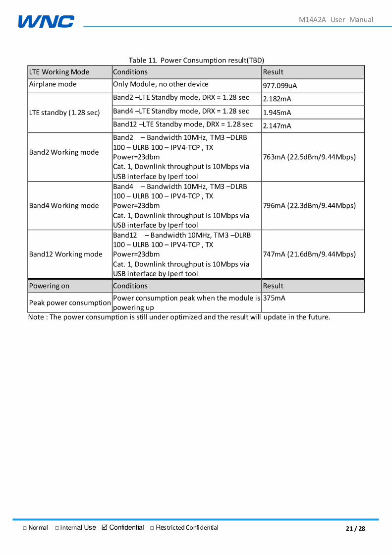
Table 11. Power Consumption result(TBD)
LTE Working Mode Conditions Result
Airplane mode Only Module, no other device 977.099uA
LTE standby (1.28 sec)
Band2 –LTE Standby mode, DRX = 1.28 sec 2.182mA
Band4 –LTE Standby mode, DRX = 1.28 sec 1.945mA
Band12 –LTE Standby mode, DRX = 1.28 sec 2.147mA
Band2 Working mode
Band2 – Bandwidth 10MHz, TM3 –DLRB
100 – ULRB 100 – IPV4-TCP , TX
Power=23dbm
Cat. 1, Downlink throughput is 10Mbps via
USB interface by Iperf tool
763mA (22.5dBm/9.44Mbps)
Band4 Working mode
Band4 – Bandwidth 10MHz, TM3 –DLRB
100 – ULRB 100 – IPV4-TCP , TX
Power=23dbm
Cat. 1, Downlink throughput is 10Mbps via
USB interface by Iperf tool
796mA (22.3dBm/9.44Mbps)
Band12 Working mode
Band12 – Bandwidth 10MHz, TM3 –DLRB
100 – ULRB 100 – IPV4-TCP , TX
Power=23dbm
Cat. 1, Downlink throughput is 10Mbps via
USB interface by Iperf tool
747mA (21.6dBm/9.44Mbps)
Powering on Conditions Result
Peak power consumption Power consumption peak when the module is
powering up
375mA
Note : The power consumption is still under optimized and the result will update in the future.

22 / 28 Normal Internal Use Confidential Restricted Confidential
M14A2A User Manual
5. Software Interface
M14A2A can be configured with several types of configurations for different external host processors
which require data communication to the Internet. The basic concept is that the module provides proper
interfaces for its control and for the data traffic, which supports as many external host processors as
possible with different capabilities for network connection.
Please refer to the WNC M 8Q M 4A A “W Developer Guide for further detail.
23 / 28 Normal Internal Use Confidential Restricted Confidential
M14A2A User Manual
6. Mechanical and Environmental Specifications
6.1. PCBA form factor
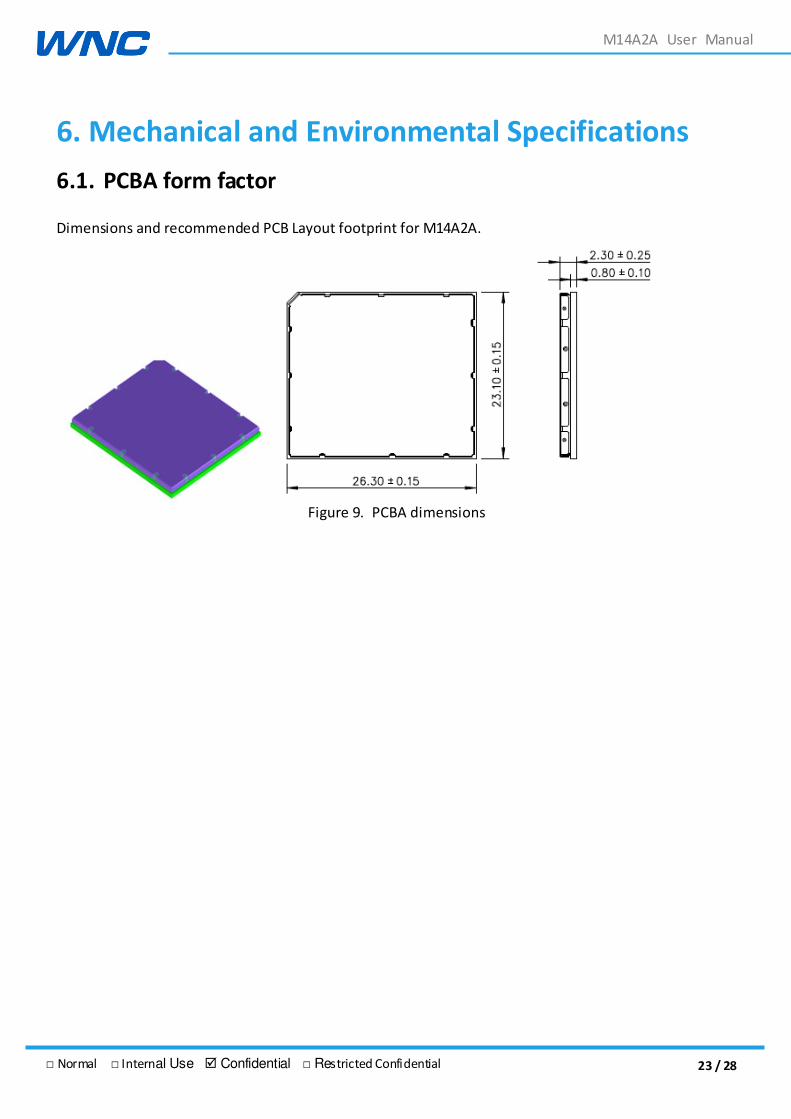
Dimensions and recommended PCB Layout footprint for M14A2A.
Figure 9. PCBA dimensions
24 / 28 Normal Internal Use Confidential Restricted Confidential
M14A2A User Manual
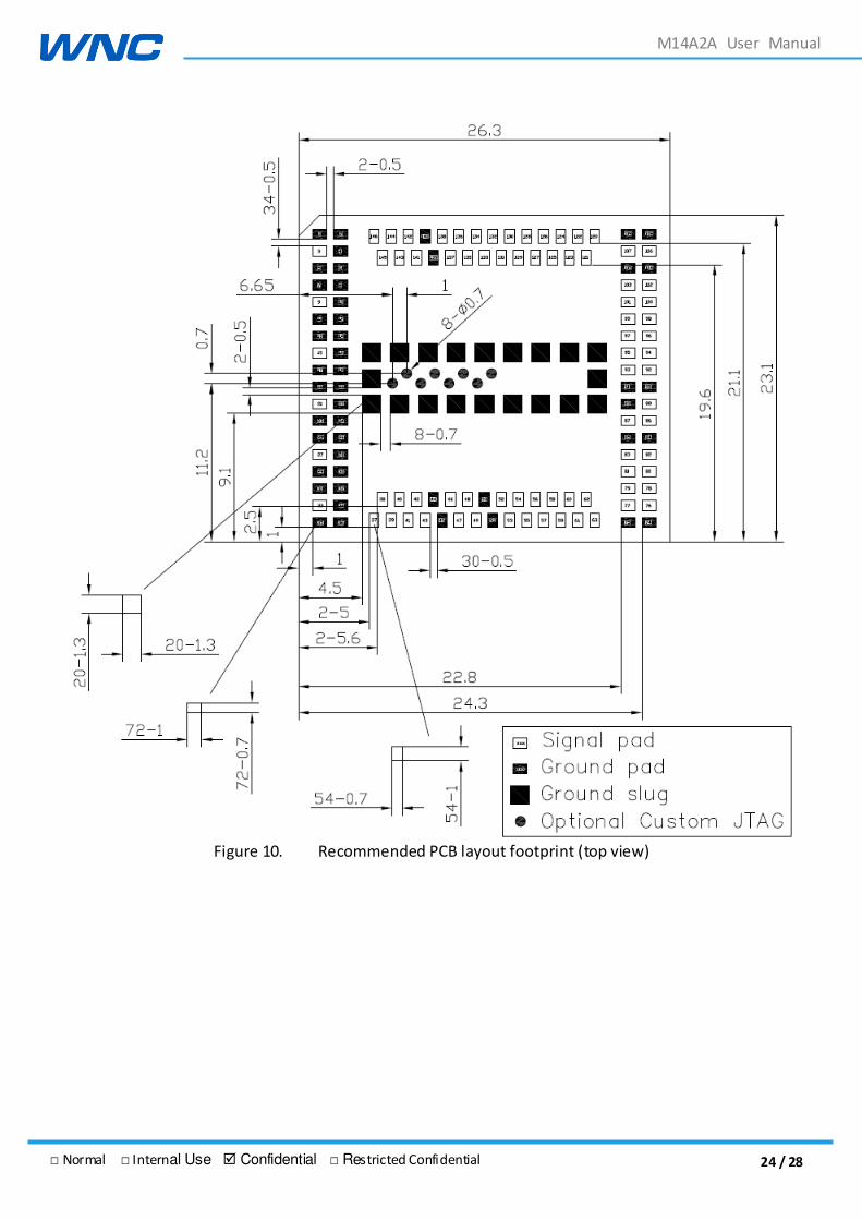
Figure 10. Recommended PCB layout footprint (top view)

25 / 28 Normal Internal Use Confidential Restricted Confidential
M14A2A User Manual
6.2. Labeling
When the module is installed in the host device, the FCC ID label must be visible through a window on
the final device or it must be visible when an access panel, door or cover is easily re-moved. If not, a
second label must be placed on the outside of the final device that contains the following text:
Co tai s FCC ID:NKRM14A2A
The grantee's FCC ID can be used only when all FCC compliance requirements are met
6.3. Thermal considerations
Ambient operating temperature: –30 °C to +75 °C
Ambient storage temperature: –40 °C to +85 °C
The case temperature of module shielding cover must be < 85 °C when integrated to prevent damage.
Design points used to improve the thermal performance:
It is better to add a naked copper area onto M14A2A’s back side of the PCB. If the thermal
performance becomes a issue in the customer’s product, add thermal solutions for
improvement such as thermal padding or a heat sink.
It’s recommended to have a thermal pad or a heat sink on shielding cover to help transfer
heat.

26 / 28 Normal Internal Use Confidential Restricted Confidential
M14A2A User Manual
7. Regulatory and Industry Approvals
7.1. Certification testing
PTCRB, FCC and AT&T TA
7.2. Safety and hazards
Be sure the use of this product is allowed in the country and in the environment required. The use of this
product may be dangerous and must be avoided in the following areas:
Where it can interfere with other electronic devices in environments such as hospitals, airports,
and aircraft
Where there is a risk of explosion such as gasoline stations and oil refineries
It is the responsibility of the user to comply with his or her country’s regulations and the specific
environmental regulations.
Do not disassemble the product; any mark of tampering will compromise the warranty’s validity.
We recommend following the instructions of the hardware user guides for a correct wiring of the
product. The product must be supplied with a stabilized voltage source, and the wiring must conform to
the security and fire-prevention regulations.
This product must be handled with care; avoid any contact with the pins because electrostatic discharge
may damage the product. Same caution must be taken regarding the SIM card; carefully check the
instructions for its use. Do not insert or remove the SIM when the product is in power-saving mode.
The system integrator is responsible of the functioning of the final product; therefore, care must be
taken for the external components of the module as well as for project or installation issues—there may
be a risk of disturbing the GSM network or external devices or of having an impact on device security. If
you have any doubts, please refer to the technical documentation and the relevant regulations in force.
Every module must be equipped with a proper antenna with specific characteristics. The antenna must
be installed with care in order to avoid any interference with other electronic devices .

27 / 28 Normal Internal Use Confidential Restricted Confidential
M14A2A User Manual
8. References
8.1. Web site support
To be updated
8.2. WNC documents
To be updated
sss

28 / 28 Normal Internal Use Confidential Restricted Confidential
M14A2A User Manual
9. Safety Recommendation
Be sure the use of this product is allowed in the country and in the environment required. The use of this
product may be dangerous and must be avoided in the following areas:
Where it can interfere with other electronic devices in environments such as hospitals,
airports, and aircraft
Where there is a risk of explosion such as gasoline stations and oil refineries
It is the responsibility of the user to comply with the his or her country’s regulations and the specific
environmental regulations.
Do not disassemble the product; any mark of tampering will compromise the warranty ’s validity.
We recommend following the instructions of the hardware user guides for a correct wiring of the
product. The product must be supplied with a stabilized voltage source, and the wiring must conform to
the security and fire-prevention regulations.
This product must be handled with care; avoid any contact with the pins because electrostatic discharge
may damage the product. Same caution must be taken regarding the SIM card; carefully check the
instructions for its use. Do not insert or remove the SIM when the product is in power-saving mode.
The system integrator is responsible of the functioning of the final product; therefore, care must be
taken for the external components of the module as well as for project or installation issues—there may
be a risk of disturbing the GSM network or external devices or of having an impact on device security. If
you have any doubts, please refer to the technical documentation and the relevant regulations in force.
Every module must be equipped with a proper antenna with specific characteristics. The antenna must
be installed with care in order to avoid any interference with other electronic devices .