M. E. (VLSI DESIGN) 2015 Regulations, Curriculum & Syllabi
57
M. E. (VLSI DESIGN) 2015 Regulations, Curriculum & Syllabi BANNARI AMMAN INSTITUTE OF TECHNOLOGY (An Autonomous Institution Affiliated to Anna University, Chennai Approved by AICTE - Accredited by NBA New Delhi, NAAC with ‘A’ Grade and ISO 9001:2008 Certified) SATHYAMANGALAM – 638 401 Erode District Tamil Nadu Phone : 04295 226000 Fax : 04295 226666 Web:www.bitsathy.ac.in E-mail : [email protected]
-
Upload
phungkhanh -
Category
Documents
-
view
221 -
download
2
Transcript of M. E. (VLSI DESIGN) 2015 Regulations, Curriculum & Syllabi
M. E. (VLSI DESIGN)
2015 Regulations, Curriculum & Syllabi
BANNARI AMMAN INSTITUTE OF TECHNOLOGY (An Autonomous Institution Affiliated to Anna University, Chennai
Approved by AICTE - Accredited by NBA New Delhi, NAAC with ‘A’ Grade and ISO 9001:2008 Certified)
SATHYAMANGALAM – 638 401 Erode District Tamil Nadu
Phone : 04295 226000 Fax : 04295 226666
Web:www.bitsathy.ac.in E-mail : [email protected]

CONTENTS
Page No.
Regulations i
PEOs xv
POs xvi
Mapping of PEOs and POs xvii
Curriculum 2015 1
Syllabi 4

PEOs & POs M.E. – VLSI Design | Regulations 2015 Approved in XII Academic Council Meeting held on 19.09.2015
xv
PROGRAMME EDUCATIONAL OBJECTIVES (PEOs)
I. The Graduates will demonstrate their outstanding education skills that will enable them to
integrate undergraduate fundamentals with the knowledge acquired to evaluate and analyze
new developments in VLSI industry.
II. The Graduates will undertake a significant research or development projects in order to suit
multi-disciplinary situations.
III. The Graduates will demonstrate their professional, ethical and social values to solve real time
problems.

PEOs & POs M.E. – VLSI Design | Regulations 2015 Approved in XII Academic Council Meeting held on 19.09.2015
xvi
PROGRAMME OUTCOMES (POs)
a. The student will acquire in-depth knowledge of VLSI design, with an ability to discriminate,
evaluate, analyse and synthesize existing and new knowledge, and integration of the same for
enhancement of knowledge.
b. The student will analyse complex VLSI problems critically, apply independent judgment for
synthesizing information to make intellectual and/or creative advances for conducting
research in a wider theoretical, practical and policy context
c. The student will think laterally and originally, conceptualize and solve problems related to
VLSI design, evaluate a wide range of potential solutions for those problems and arrive at
feasible, optimal solutions after considering public health and safety, cultural, societal and
environmental factors in the core areas of VLSI.
d. The student will extract information pertinent to unfamiliar problems through literature
survey and experiments, apply appropriate research methodologies, techniques and tools,
design, conduct experiments, analyse and interpret data, demonstrate higher order skill and
view things in a broader perspective, contribute individually/in group(s) to the development
of scientific/technological knowledge in VLSI domain.
e. The student will Create, select, learn and apply appropriate techniques, resources, and
modern engineering and IT tools, including prediction and modeling, to complex VLSI
activities with an understanding of the limitations
f. The student will Possess knowledge and understanding of group dynamics, recognize
opportunities and contribute positively to collaborative-multidisciplinary scientific research,
demonstrate a capacity for self-management and teamwork, decision-making based on open-
mindedness, objectivity and rational analysis in order to achieve common goals and further
the learning of themselves as well as others
g. The student will demonstrate knowledge and understanding of engineering and management
principles related to VLSI and apply the same to one’s own work, as a member and leader in
a team, manage projects efficiently in VLSI and multidisciplinary environments after
consideration of economic and financial factors.
h. The student will be able to Communicate with the VLSI community, and with society at
large, regarding complex VLSI activities confidently and effectively, such as, being able to
comprehend and write effective reports and design documentation by adhering to appropriate
standards, make effective presentations, and give and receive clear instructions.
i. The student will be able to recognize the need for, and have the preparation and ability to
engage in life-long learning independently, with a high level of enthusiasm and commitment
to improve knowledge and competence continuously.
j. The student will acquire professional and intellectual integrity, professional code of conduct,
ethics of research and scholarship, consideration of the impact of research outcomes on
professional practices and an understanding of responsibility to contribute to the community
for sustainable development of society.
k. The student will observe and examine critically the outcomes of one’s actions and make
corrective measures subsequently, and learn from mistakes without depending on external
feedback.

PEOs & POs M.E. – VLSI Design | Regulations 2015 Approved in XII Academic Council Meeting held on 19.09.2015
xvii
MAPPING OF PEOs AND POs
PEO(s) Programme Outcome (s)
(a) (b) (c) (d) (e) (f) (g) (h) (i) (j) (k)
I x x x x
II x x x
III x x x x
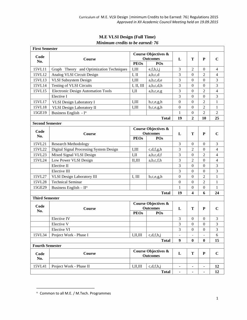
Curriculum of M.E. VLSI Design |minimum Credits to be Earned: 76| Regulations 2015 Approved in XII Academic Council Meeting held on 19.09.2015
1
M.E VLSI Design (Full Time)
Minimum credits to be earned: 76
First Semester
Code
No. Course
Course Objectives &
Outcomes L T P C PEOs POs
15VL11 Graph Theory and Optimization Techniques I,III e,f,h,i,j 3 2 0 4
15VL12 Analog VLSI Circuit Design I, II a,b,c,d 3 0 2 4
15VL13 VLSI Subsystem Design I,III a,b,c,d,e 3 0 0 3
15VL14 Testing of VLSI Circuits I, II, III a,b,c,d,h 3 0 0 3
15VL15 Electronic Design Automation Tools I,II a,b,c,e,g 3 0 2 4
Elective I 3 0 0 3
15VL17 VLSI Design Laboratory I I,III b,c,e,g,h 0 0 2 1
15VL18 VLSI Design Laboratory II I,III b,c,e,g,h 0 0 2 1
15GE19 Business English - I 1 0 2 2
Total 19 2 10 25
Second Semester
Code
No. Course
Course Objectives &
Outcomes L T P C PEOs POs
15VL21 Research Methodology 3 0 0 3
15VL22 Digital Signal Processing System Design I,III c,d,f,g,h 3 2 0 4
15VL23 Mixed Signal VLSI Design I,II a,b,c,d,f 3 0 2 4
15VL24 Low Power VLSI Design II,III a,b,c,f,h 3 2 0 4
Elective II 3 0 0 3
Elective III 3 0 0 3
15VL27 VLSI Design Laboratory III I, III b,c,e,g,h 0 0 2 1
15VL28 Technical Seminar 0 0 2 1
15GE29 Business English – II 1 0 0 1
Total 19 4 6 24
Third Semester
Code
No. Course
Course Objectives &
Outcomes L T P C PEOs POs
Elective IV 3 0 0 3
Elective V 3 0 0 3
Elective VI 3 0 0 3
15VL34 Project Work - Phase I I,II,III c,d,f,h,j - - - 6
Total 9 0 0 15
Fourth Semester
Code
No.
Course Course Objectives &
Outcomes L T P C
15VL41 Project Work - Phase II I,II,III c,d,f,h,j - - - 12
Total - - - 12
Common to all M.E. / M.Tech. Programmes

Curriculum of M.E. VLSI Design |minimum Credits to be Earned: 76| Regulations 2015 Approved in XII Academic Council Meeting held on 19.09.2015
2
M.E VLSI Design (Part Time) First Semester
Code No. Course Objectives & Outcomes
L T P C PEOs POs
15VL11 Graph Theory and Optimization
Techniques I,III e,f,h,i,j 3 2 0 4
15VL12 Analog VLSI Circuit Design I,II a,b,c,d 3 0 2 4
15VL13 VLSI Subsystem Design I,III a,b,c,d,e 3 0 0 3
15VL17 VLSI Design Laboratory I I,III b,c,e,g,h 0 0 2 1
15GE19 Business English - I 1 0 2 2
Total 10 2 6 14
Second Semester
Code No. Course Objectives & Outcomes
L T P C PEOs POs
15VL21 Research Methodology 3 0 0 3
15VL22 Digital Signal Processing System Design I,III c,d,f,g,h 3 2 0 4
15VL23 Mixed Signal VLSI Design I,II a,b,c,d,f 3 0 2 4
15VL27 VLSI Design Laboratory III I,III b,c,e,g,h 0 0 2 1
15GE29 Business English – II 1 0 0 1
Total 10 2 4 13
Third Semester
Code No. Course Objectives & Outcomes
L T P C PEOs POs
15VL14 Testing of VLSI Circuits I,II, III a,b,c,d,h 3 0 0 3
15VL15 Electronic Design Automation Tools I,II a,b,c,e,g 3 0 2 4
15VL24 Low Power VLSI Design II,III a,b,c,f,h 3 2 0 4
15VL18 VLSI Design Laboratory II I,III b,c,e,g,h 0 0 2 1
Total 9 2 4 12
Fourth Semester
Code No. Course Objectives & Outcomes
L T P C PEOs POs
Elective I 3 0 0 3
Elective II 3 0 0 3
Elective III 3 0 0 3
15VL28 Technical Seminar 0 0 2 1
Total 9 0 2 10
Fifth Semester
Code No. Course Objectives & Outcomes
L T P C PEOs POs
Elective IV 3 0 0 3
Elective V 3 0 0 3
Elective VI 3 0 0 3
15VL34 Project Work - Phase I I,II,III c,d,f,h,j - - - 6
Total 9 0 0 15
Sixth Semester
Code No. Course Objectives & Outcomes
L T P C PEOs POs
15VL41 Project Work - Phase II I,II,III c,d,f,h,j - 12
Common to all M.E. / M.Tech. Programmes

Curriculum of M.E. VLSI Design |minimum Credits to be Earned: 76| Regulations 2015 Approved in XII Academic Council Meeting held on 19.09.2015
3
List of Electives
Code No. Course
Course Objectives
& Outcomes L T P C
PEOs POs
15VL51 ASIC Design I,III a,c,d,e,f 3 0 0 3
15VL52 Physical Design Automation I,II a,b,c,d,e 3 0 0 3
15VL53 System on Chip I,III a,b,c,e,f 3 0 0 3
15VL54 Advanced Digital System Design I,II c,e,f,g 3 0 0 3
15VL55 DSP Integrated Circuits I,III a,b,c,d,e 3 0 0 3
15VL56 Semiconductor Memory Design I,III c,d,f,g,h 3 0 0 3
15VL57 Hardware Design Verification
Techniques I,II a,b,c,f,i 3 0 0 3
15VL58 VLSI Technology I,III c,e,f,g 3 0 0 3
15VL59 System Design using FPGA I,II a,b,c,d,e 3 0 0 3
15VL60 CMOS RF Circuit Design I,II a,b,c,f,g 3 0 0 3
15VL61 VLSI Signal Processing I,II a,c,f,i.j 3 0 0 3
15VL62 Memory Design and Testing I,III a,b,e,h,j 3 0 0 3
15VL63 Communication Networks I,II a,b,c,f,g 3 0 0 3
15VL64 Network on chip I,II a,b,c,d 3 0 0 3
15VL65 Reconfigurable Architectures I,III a,b,c,d,e 3 0 0 3
15VL66 Processors and Embedded controllers I,II a,b,c,e.h 3 0 0 3
15VL67 ARM Processor and Applications I,III a,b,c,e,g 3 0 0 3
15VL68 Embedded Networking I,II a,b,c,e,g 3 0 0 3
15VL69 Nano Electronic Devices I,III a,b,c,e,i 3 0 0 3
15VL70 MEMS 3 0 0 3
15VL71 Genetic algorithms and their
Applications I,III a,c,d,e,f 3 0 0 3
15VL72 VLSI for Wireless Communication I,II a,b,c,d 3 0 0 3
15VL73 Thermal Analysis and Power
Management of Integrated Circuits I,III e,f,g,h 3 0 0 3
One Credit Courses
Code No. Course
Course Objectives
& Outcomes L T P C
PEOs POs
15VLXA FPGA based VLSI design I,III a,c,d,e,f 1 0 0 1
15VLXB Backend design of digital circuits I a,b,c,d,e 1 0 0 1
15VLXC Backend design of analog circuits I a,b,c,d,e 1 0 0 1
Common to VLSI Design and Embedded Systems Common to VLSI Design and Applied Electronics
Syllabi: M.E. VLSI Design |minimum Credits to be Earned: 76| Regulations 2015 Approved in XII Academic Council Meeting held on 19.09.2015
4
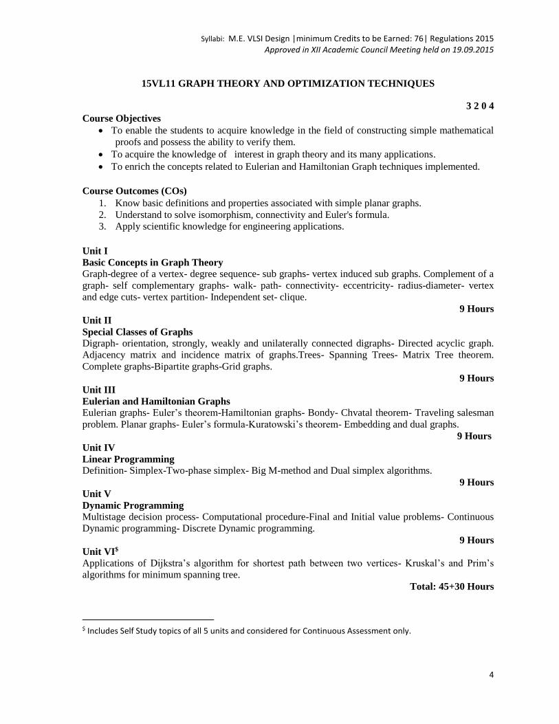
15VL11 GRAPH THEORY AND OPTIMIZATION TECHNIQUES
3 2 0 4
Course Objectives
To enable the students to acquire knowledge in the field of constructing simple mathematical
proofs and possess the ability to verify them.
To acquire the knowledge of interest in graph theory and its many applications.
To enrich the concepts related to Eulerian and Hamiltonian Graph techniques implemented.
Course Outcomes (COs) 1. Know basic definitions and properties associated with simple planar graphs.
2. Understand to solve isomorphism, connectivity and Euler's formula.
3. Apply scientific knowledge for engineering applications.
Unit I
Basic Concepts in Graph Theory
Graph-degree of a vertex- degree sequence- sub graphs- vertex induced sub graphs. Complement of a
graph- self complementary graphs- walk- path- connectivity- eccentricity- radius-diameter- vertex
and edge cuts- vertex partition- Independent set- clique.
9 Hours
Unit II
Special Classes of Graphs
Digraph- orientation, strongly, weakly and unilaterally connected digraphs- Directed acyclic graph.
Adjacency matrix and incidence matrix of graphs.Trees- Spanning Trees- Matrix Tree theorem.
Complete graphs-Bipartite graphs-Grid graphs.
9 Hours
Unit III
Eulerian and Hamiltonian Graphs
Eulerian graphs- Euler’s theorem-Hamiltonian graphs- Bondy- Chvatal theorem- Traveling salesman
problem. Planar graphs- Euler’s formula-Kuratowski’s theorem- Embedding and dual graphs.
9 Hours
Unit IV
Linear Programming
Definition- Simplex-Two-phase simplex- Big M-method and Dual simplex algorithms.
9 Hours
Unit V
Dynamic Programming
Multistage decision process- Computational procedure-Final and Initial value problems- Continuous
Dynamic programming- Discrete Dynamic programming.
9 Hours
Unit VI$
Applications of Dijkstra’s algorithm for shortest path between two vertices- Kruskal’s and Prim’s
algorithms for minimum spanning tree.
Total: 45+30 Hours
$ Includes Self Study topics of all 5 units and considered for Continuous Assessment only.
Syllabi: M.E. VLSI Design |minimum Credits to be Earned: 76| Regulations 2015 Approved in XII Academic Council Meeting held on 19.09.2015
5
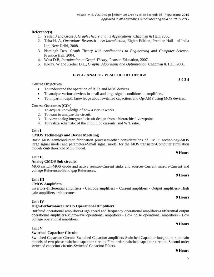
Reference(s)
1. Yellen J and Gross J, Graph Theory and its Applications, Chapman & Hall, 2006.
2. Taha H. A, Operations Research – An Introduction, Eighth Edition, Prentice Hall of India
Ltd, New Delhi, 2008.
3. Narsingh Deo, Graph Theory with Applications to Engineering and Computer Science.
Prentice Hall, 2004.
4. West D.B, Introduction to Graph Theory, Pearson Education, 2007.
5. Kocay. W and Kreher D.L., Graphs, Algorithms and Optimization, Chapman & Hall, 2006.
15VL12 ANALOG VLSI CIRCUIT DESIGN 3 0 2 4
Course Objectives To understand the operation of BJTs and MOS devices.
To analyze various devices in small and large signal conditions in amplifiers.
To impart in-depth knowledge about switched capacitors and Op-AMP using MOS devices.
Course Outcomes (COs) 1. To acquire knowledge of how a circuit works.
2. To learn to analyze the circuit.
3. To view analog integrated circuit design from a hierarchical viewpoint. 4. To realize schematic of the circuit, dc currents, and W/L ratio.
Unit I CMOS Technology and Device Modeling Basic MOS semiconductor fabrication processes-other considerations of CMOS technology-MOS large signal model and parameters-Small signal model for the MOS transistor-Computer simulation models-Sub threshold MOS model.
9 Hours
Unit II Analog CMOS Sub circuits, MOS switch-MOS diode and active resistor-Current sinks and sources-Current mirrors-Current and voltage References-Band gap References.
9 Hours
Unit III CMOS Amplifiers
Invertors-Differential amplifiers - Cascode amplifiers – Current amplifiers - Output amplifiers- High
gain amplifiers architectures
9 Hours
Unit IV High-Performance CMOS Operational Amplifiers Buffered operational amplifiers-High speed and frequency operational amplifiers-Differential output operational amplifiers-Microwave operational amplifiers - Low noise operational amplifiers - Low voltage operational amplifiers.
9 Hours Unit V Switched Capacitor Circuits Switched Capacitor Circuits-Switched Capacitor amplifiers-Switched Capacitor integrators-z domain models of two phase switched capacitor circuits-First order switched capacitor circuits- Second order switched capacitor circuits-Switched Capacitor Filters.
9 Hours

Syllabi: M.E. VLSI Design |minimum Credits to be Earned: 76| Regulations 2015 Approved in XII Academic Council Meeting held on 19.09.2015
6
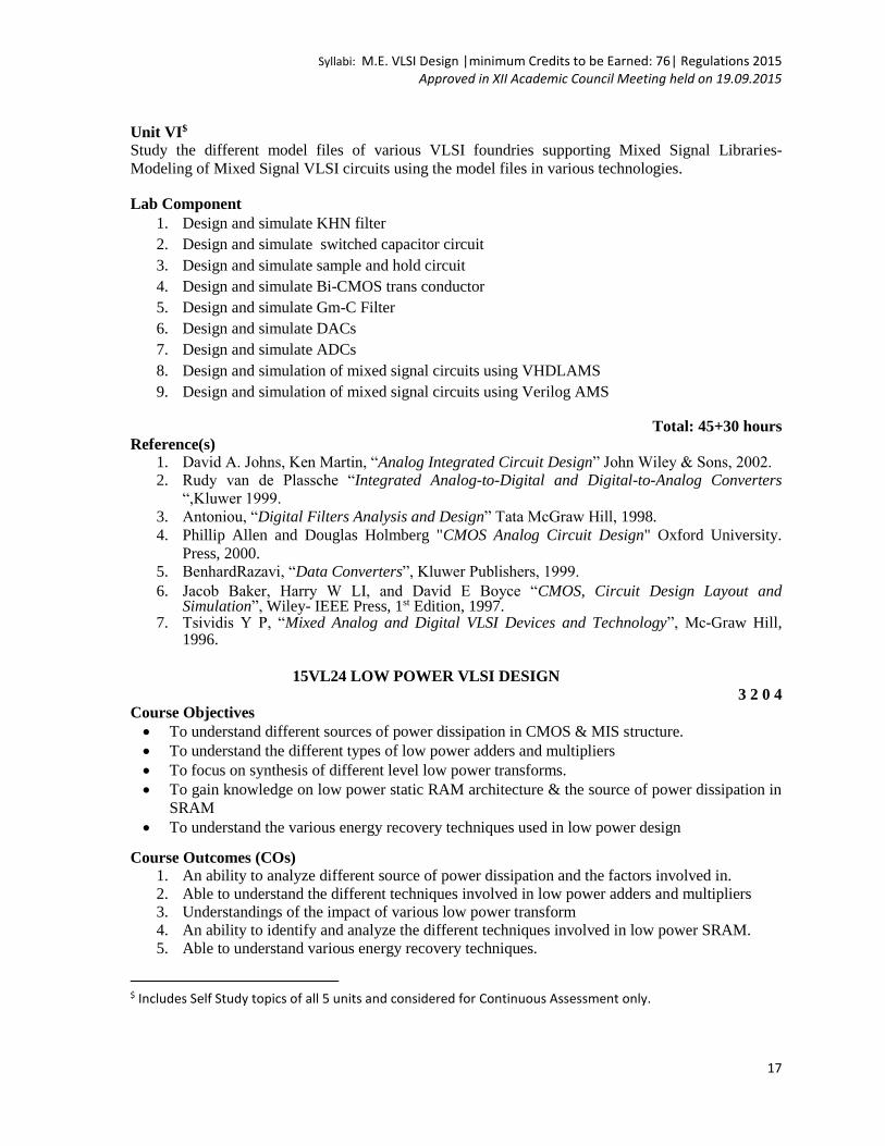
Unit VI$
Study the different model files of various VLSI foundries supporting Analog Libraries- Modeling of
Analog VLSI circuits using the model files in various technologies. Total: 45+ 30 Hours
List of Experiments:
1. Characterization of NMOS and PMOS
2. Simulation of Active Resistor, switch and diode
3. Simulation of Current Source and Current Sink
4. Simulation of Current mirror
5. Simulation of band gap references
6. Simulation of Common Source amplifiers
7. Simulation of differential amplifiers
8. Simulation of operational amplifiers
9. Simulation of Switched capacitor circuits
Reference(s) 1. Phillip E.Allen and Douglas R.Holberg, CMOS Analog Circuit Design, Oxford University
Press, 2002. 2. Malcom R.Haskard and LanC. May, Analog VLSI Design - NMOS and CMOS, Prentice Hall,
1998. 3. Jose E.France and Yannis Tsividis, Design of Analog-Digital VLSI Circuits for
Telecommunication and Signal Processing, Prentice Hall, 1994. 4. Randall L Geiger, Phillip E. Allen and Noel K.Strader, VLSI Design Techniques for Analog
and Digital Circuits, McGraw Hill International Company, 1990. 5. K.Radhakrishna Rao, Electronics for Analog Signal Processing-I, NPTEL, Courseware,
2005. 15VL13 VLSI SUBSYSTEM DESIGN
3 0 0 3
Course Objectives To learn the basic MOS Circuits
To learn the MOS Process Technology
To understand the operation of MOS devices. To impart in-depth knowledge about analog and digital CMOS circuits.
Course Outcomes (CO’s) 1. Analysis the operation of CMOS. 2. Analysis of the design rules and layout diagrams.
3. Design of low power Adders and Multipliers.
4. Analysis the physical design process of VLSI design flow.
5. Design of CMOS Memories.
Unit I MOS Circuit Design Process Overview of VLSI Design Methodology VLSI design process- Basic MOS transistors- Enhancement mode transistor operation - Drain current Vs voltage derivation -NMOS inverter- Determination of
$ Includes Self Study topics of all 5 units and considered for Continuous Assessment only.

Syllabi: M.E. VLSI Design |minimum Credits to be Earned: 76| Regulations 2015 Approved in XII Academic Council Meeting held on 19.09.2015
7
pull up to pull down ratio for an NMOS inverter-CMOS inverter - DC Characteristics- Switching Characteristics – Power dissipation.
9 Hours Unit II Logic Design Pass transistor and transmission gate – static CMOS design, Pseudo NMOS, and dynamic CMOS logic – Clocked CMOS logic – domino logic- Precharged domino logic, Dual rail logic with suitable examples.
9 Hours Unit III Sequential Logic Clocked sequential circuits – Two phase clocking – charge storage – dynamic sequential circuits – JK Flip-flop circuit, Memory Design-DRAM, SRAM and Flash Memory.
9 Hours
Unit IV
Data path Subsystem Introduction, Design of Adders: carry look ahead - carry select - carry save, One/Zero Detector, Comparator-Magnitude, Equality, Counters-Binary Counter, LFSR, Parity generators.
9 Hours Unit V VLSI Building Block Design PLA design – Arithmetic logic unit design- Design of multipliers: Parallel Multipliers, Array, 2’s Complement, Booth - Braun – Baugh - Wooley - Wallace tree, Dadda Multipliers, Serial Multiplication.
9 Hours Unit VI$
Design and Simulation of VLSI circuits
nMOS inverter- domino logic- two phase clocking-LFSR
Total: 45 Hours Reference(s)
1. Kamran Eshraghian, Douglas A. Pucknell, Essentials of VLSI Circuits and Systems, Prentice Hall of India, 2011
2. John P.Uyemura, Introduction to VLSI circuits and systems, John Wiley & Sons, 2012. 3. Neil Weste and Kamran Eshranghian, Principles of CMOS VLSI Design, Addison Wiley,
2012. 4. Jan M Rabaey, Digital Integrated Circuits- A Design, Prentice Hall, 2009. 5. C.Mead and L.Conway, Introduction to VLSI Systems, Addison Wesley, 1999. 6. Kang, CMOS Digital integrated Circuits, McGraw Hill, 2002. 7. L.Glaser and D.Dobberpuhl, The Design and Analysis of VLSI Circuits, Addison Wesley,
1995.
8. S.Srinivasan, VLSI Circuits, NPTEL Courseware, 2005.
$ Includes Self Study topics of all 5 units and considered for Continuous Assessment only.

Syllabi: M.E. VLSI Design |minimum Credits to be Earned: 76| Regulations 2015 Approved in XII Academic Council Meeting held on 19.09.2015
8
15VL14 TESTING OF VLSI CIRCUITS 3 0 0 3
Course Objectives: To understand about testing, fault models and types of simulations.
To acquire knowledge in generation of test vectors for combinational and sequential circuits.
To understand the concepts behind testable design, BIST and fault diagnosis.
Course Outcomes (CO’s) 1. Ability to know about importance of testing and its types in VLSI circuits.
2. Ability to model different faults and carry out fault simulation in digital circuits.
3. Ability to determine fault oriented test vectors for single stuck-at-faults in combinational and Sequential circuits.
4. Ability to design digital VLSI circuits with DFT and BIST techniques.
Unit I Fault Simulation Introduction to Testing - Faults in digital circuits - Modeling of faults - Logical Fault Models - Fault detection - Fault location - Fault dominance - Logic Simulation - Types of simulation - Delay models - Gate level Event-driven simulation.
9 Hours Unit II Test Generation Test generation for combinational logic circuits - Testable combinational logic circuit design - Test generation for sequential circuits - design of testable sequential circuits- Adhoc design and scan based design techniques.
9 Hours Unit III Analog and Mixed Signal Test DSP based analog and mixed signal test – Static ADC and DAC testing methods - Model based Analog and mixed signal Test- Analog fault models-Analog fault simulation – Analog ATPG
9 Hours Unit IV Built In Self-Test Built-In Self-Test - Test pattern generation for BIST - Circular BIST - BIST Architectures – BEST – LOCST - STUMPS - CATS – BILBO - Testable Memory Design - Test algorithms - Test generation for Embedded RAMs
9 Hours
Unit V Fault Diagnosis Logic Level Diagnosis - Diagnosis by UUT reduction - Fault Diagnosis for Combinational Circuits - Self-checking design: error detecting and correcting codes, self checking combinational logic, sequential logic design: Faults in State Machines, Self-Checking State Machine Design Techniques, Elimination of Bidirectional Errors
9 Hours

Syllabi: M.E. VLSI Design |minimum Credits to be Earned: 76| Regulations 2015 Approved in XII Academic Council Meeting held on 19.09.2015
9
Unit VI$ Designing of testing circuits for various applications and simulation
Testing of circuits for analog and digital faults-ATPG
Total: 45 Hours Reference(s)
1. Abramovici .M, Breuer M.A and Friedman A.D, Digital Systems and Testable Design, Jaico Publishing House, 2002.
2. Bushnell M.L and Agrawal V.D, Essentials of Electronic Testing for Digital, Memory and Mixed-Signal VLSI Circuits, Kluwer Academic Publishers, 2002.
3. Lala P.K, Digital Circuit Testing and Testability, Academic Press, 2002. 4. Parag K. Lala, Self-checking and fault-tolerant digital design, Morgan Kaufmann, 2001.
5. Xiaoqing Wen, Cheng Wen Wu and Laung Terng Wang, VLSI Test Principles and
Architectures: Design for Testability, Cambridge University Press, 2000
15VL15 ELECTRONIC DESIGN AUTOMATION TOOLS 3 0 2 4
Course Objectives To study the features of various VLSI EDA Tools.
To study the concepts of simulation and synthesis of HDLs.
To understand the concepts of SPICE and circuit simulation using Spice.
Course Outcomes (COs) 1. Explain various features of EDA tools.
2. Model the various Digital Circuits using HDL
3. Select appropriate analysis for circuit design 4. Sketch the Layout of simple logic circuits
Unit I Basics of EDA Tools VLSI Design Automation tools-An overview of the features of practical CAD tools – FPGA Technology & Tools - Modelsim - Leonardo spectrum -Xilinx ISE - Quartus II – ASIC Technology & Tools – Pyxis, Cadence, Synopsys and Microwind.
9 Hours
Unit II
Basics of Verilog HDL and Modeling
Importance of HDL, Design Methodologies, Basic Concepts- Lexical Conventions- Data Types-
Verilog Operators- Modules and Ports - Types of Modeling- Gate-Level Modeling, Dataflow
Modeling, Behavioral Modeling, Switch Level Modeling- Design Examples using Combinational &
Sequential Logic
9 Hours
Unit III
Advanced Verilog HDL and Verilog Test Benches
Finite State Machines (FSM) Synthesis in Verilog, Memory Design – Single Port and Dual Port
SRAM, Tasks, Functions, User Defined Primitives (UDP)- Timing and Delays, Compiler Directives-
$ Includes Self Study topics of all 5 units and considered for Continuous Assessment only.

Syllabi: M.E. VLSI Design |minimum Credits to be Earned: 76| Regulations 2015 Approved in XII Academic Council Meeting held on 19.09.2015
10
Verilog Test Benches for Combinational Logic Modules and Sequential Digital Circuits, Applications
oriented system design.
9 Hours Unit IV
VHDL Data Types, Operators, Classes of Objects, entities and architectures, Attributes – concurrent statements – sequential statements – signals and variables – Behavior, dataflow and structural modeling – Configurations, functions – procedures – packages – test benches – Design examples
9 Hours Unit V
Analysis of SPICE& Layout Design Introduction - Types of SPICE – Types of Analysis - Circuit description - DC circuit analysis-
Transient analysis - AC circuit analysis - Advanced spice commands and analysis – VLSI Layout –
Design Rules – Stick Diagram – Example Layout of digital logic circuits using EDA Tools.
9 Hours
Unit VI$
Design flow in EDA tools for FPGA based design and ASIC based Design. Comparisons between
PLDs CPLD and FPGAs - Interfacing Matlab Simulink with Xilinx ISE - DSP Application using
Xilinx System Generator Lab Components
1. Model a 16 Bit Magnitude Comparator using Behavioral HDL
2. Design a 32 Bit ALU using Behavioral HDL
3. Design a Universal shift register using Structural HDL Modeling
4. Generate a Random Number using Structural HDL Modeling
5. Vending machine Controller using FSM
6. Traffic Light Controller using FSM
7. Perform AC, DC, Transient Analysis of CMOS Amplifier using EDA Tools
8. Layout of Combinational Circuit Using EDA Tools. Total: 45+30 Hours
Reference(s)
1. Ming-Bo Lin, Digital System Designs and Practices using Verilog HDL and FPGAs, Wiley,
2012.
2. Samir Palnitkar, Verilog HDL, Pearson Education, 2ndEdition, 2004.
3. M.H.Rashid, Spice for Circuits and Electronics using Pspice, PHI 1995. 4. M.J.S.Smith, Application Specific Integrated Circuits, Pearson Education, 2008. 5. J.Bhaskar, A VHDL Primer, Prentice Hall, 1998. 6. J.Bhaskar, A Verilog Primer, Prentice Hall, 2005.
$ Includes Self Study topics of all 5 units and considered for Continuous Assessment only.

Syllabi: M.E. VLSI Design |minimum Credits to be Earned: 76| Regulations 2015 Approved in XII Academic Council Meeting held on 19.09.2015
11
15VL17 VLSI DESIGN LABORATORY-I 0 0 2 1
Course Objectives: To know and understand HDL and design circuits using it. To learn the student will be able to, Write programs in VHDL and Verilog for modelling
digital circuits
To study and verify the combinational and sequential logic circuits with various levels of modeling and EDA Tools.
To study this course the student will know basic electronics involved in the design of MOS
circuits.
Course Outcomes (COs)
1. By studying this subject the student will be able to make models of transistor circuits and simulate them for various operational requirements.
2. Design of different types of adders and multiplier using EDA Tool. 3. Design of FSM using EDA Tool.
4. Analysis and design of VLSI circuits. LIST OF EXPERIMENTS HDL SIMULATION AND IMPLEMENTATION IN FPGA:
1. Design and simulation of combinational circuits using HDL. 2. Design and simulation of Sequential circuits using HDL.
3. Writing Test benches using VHDL/ Verilog. 4. Design and simulation of 8-Bit shift register using HDL.
5. Design and simulation of 4-bit carry save adder, Ripple carry adder using HDL. 6. Design and simulation of 8-bit adder / subtractor using HDL. 7. Design and simulation of Multiplier using HDL 8. Design and simulation of FSM using HDL. 9. Design and Implementation of Traffic Light Controller using VHDL. 10. Synthesis the ASIC Flow Determine the area and power TB 11. Single Input SRAM
12. Mini project
Total: 30 Hours 15VL18 VLSI DESIGN LABORATORY II
0 0 2 1
Course Objectives:
To get experience and knowledge about testing and fault diagnosis of VLSI circuits.
To understand the design of various minimum spanning tree and search algorithms.
To use backend tools for simulating circuits and finding the characteristics of the circuits
Course Outcomes (COs) 1. Testing knowledge skills get improved. 2. Ability to visualize VLSI circuits. 3. Design of.
LIST OF EXPERIMENTS
FRONT-END EDA TOOL EXPERIMENTS: 1. Design and simulation of circuits for Fault simulation and
fault diagnosis a)Fault detection b)Fault location
2. Design and simulation of circuits for gate level event driven simulation

Syllabi: M.E. VLSI Design |minimum Credits to be Earned: 76| Regulations 2015 Approved in XII Academic Council Meeting held on 19.09.2015
12
3. Design and simulation of BIST architectures BACK-END EDA TOOL EXPERIMENTS: (Schematic and Layout)
1. Design and Implementation of combinational circuits using EDA Tools. 2. Test bench creation for Combinational circuits.
3. Design and Implementation of Sequential Circuit using EDA Tools. 4. Design and simulation of Adders using EDA Tools 5. CMOS, Pseudo NMOS, Dynamic & Domino Logic, CVSL
6. Layout of CMOS Inverter
7. CMOS SRAM Design, DRC, LVS & Parasitic Extraction 8. Mini project
Total: 30 Hours
15GE19 BUSINESS ENGLISH - I
1 0 2 2
Course Objectives
To acquire skills for using English in workplace effectively.
To communicate for essential business needs.
To prepare students for taking BEC Vantage level examination which is an International
Benchmark for English language proficiency of Cambridge English Language Assessment
(CELA).
Course Outcome (COs)
1. To enable students to get International recognition for work and study.
2. To use English confidently in the International business environments.
3. To be able to take part in business discussion, read company literature, write formal and
informal business correspondences and listen and understand business conversations.
UNIT I
GRAMMAR AND VOCABULARY
Comparison of adjectives – forming questions – asking complex questions – expressing purpose and
function – tenses – conditionals – time statements – modal verbs – active and passive voice – articles
– direct and indirect speech – cause and effect – relative pronouns – expressions followed by – ing
forms – countable / uncountable – acronyms – marketing terms / vocabulary – financial terms –
collocations – discourse markers.
10 Hours
UNIT II
LISTENING
Purposes of listening – features of listening texts – potential barriers to listening – specific listening
skills – strategies to use when listening– distinguishing relevant from irrelevant information – gap
filling exercise – multiple-choice options – note completion – matching and multiple choice questions
– listening for specific information, gist, topic, context and function.
7 Hours
UNIT III
SPEAKING
Word and sentence stress – clear individual sounds – turn taking – initiating and responding -
intonation patterns – pronunciation – mother tongue intrusion– conversation practice – turn-taking
and sustaining the interaction by initiating and responding appropriately.
10 Hours

Syllabi: M.E. VLSI Design |minimum Credits to be Earned: 76| Regulations 2015 Approved in XII Academic Council Meeting held on 19.09.2015
13
UNIT IV
READING
Purposes of reading – potential barriers to reading – paraphrasing – identifying facts and ideas –
skimming and scanning for information – matching statements with texts– spotting reference words –
understanding text structure – understanding the ideas in a text – distinguishing between the correct
answer and the distractor – understanding cohesion in a text – deciphering contextual meaning of
words and phrases – cloze – proof reading - transcoding.
8 Hours
UNIT V
WRITING
Paragraphing a text – using appropriate connectives – editing practice –Longer Documents: writing a
proposal.
10 Hours
Total: 45 Hours
Reference Books:
1. Guy Brook-Hart, “BEC VANTAGE: BUSINESS BENCHMARK Upper-Intermediate –
Student’s Book”, 1st Edition, Cambridge University Press, New Delhi, 2006.
2. Cambridge Examinations Publishing, “Cambridge BEC VANTAGE – Self-study Edition”,
Cambridge University Press, UK, 2005.
15VL21 - RESEARCH METHODOLOGY
3 0 0 3
Course Objectives
To import the knowledge on analysis of Research methodology
The students will be able to estimate the performance of different testing method for
research.
Course Outcomes (Cos)
1. The Students will be able to analysis the methods used for data collection hypothesis testing
and sampling process for research methodology
Unit I
Introduction
Definition, mathematical tools for analysis, Types of research, exploratory research, conclusive
research, modeling research, algorithmic research, Research process- steps.
Data collection methods- Primary data – observation method, personal interview, telephonic
interview, mail survey, questionnaire design. Secondary data- internal sources of data, external
sources of data.
9 Hours
Unit II
Sampling Methods
Scales – measurement, Types of scale – Thurstone’s Case V scale model, Osgood’s Semantic
Differential scale, Likert scale, Q- sort scale. Sampling methods- Probability sampling methods –
simple random sampling with replacement, simple random sampling without replacement, stratified
sampling, cluster sampling. Non-probability sampling method – convenience sampling,
judgment sampling, quota sampling.
9 Hours
Unit III
Hypotheses Testing
Testing of hypotheses concerning means -one mean and difference between two means -one tailed
and two tailed tests, concerning variance – one tailed Chi-square test.
9 Hours

Syllabi: M.E. VLSI Design |minimum Credits to be Earned: 76| Regulations 2015 Approved in XII Academic Council Meeting held on 19.09.2015
14
Unit IV
Research in VLSI
Top down approach and Bottom-up approach, VLSI system concept- system design- logic/circuit design-prototype chip design-engineering sample design-design revision-volume production.
9 Hours
Unit V
VLSI research forecasting models and Report writing Short-term forecasting using econometric models- long-term forecasting using technological market
models- judgment and nonlinear analysis for enhancing forecast accuracy. Report writing- Types of report, guidelines to review report, typing instructions, oral presentation.
9 Hours
Unit VI$
Case Study: apply Research Methodology principles into VLSI design and manufacturing field.
Total: 45 Hours
References
1. 1. Kothari, C.R., Research Methodology –Methods and techniques, New Age
Publications, New Delhi, 2009.
2. Panneerselvam, R., Research Methodology, Prentice-Hall of India, New Delhi, 2004.
3. Yoshio Nishi .,VLSI/ULSI RESEARCH METHODOLOGY IN THE U.S. AND JAPAN,
IEEE VLSI Technology, Systems and Application conference, 1991.
4. www.vlsiresearch.com
15VL22 DIGITAL SIGNAL PROCESSING SYSTEM DESIGN
3 2 0 4
Course Objectives
To understand the concept of DSP Processor Architecture and Programming.
To design FFT algorithm and study the concept of Code approximation in DSP system
Design.
To study the concept of Frame processing, Real Time analysis and Scheduling in DSP system
Design.
Course Outcomes (COs)
1. Understand the architecture of DSP processor.
2. Design and analysis the digital filters. 3. Learn CCS and analysis the code optimization. 4. Understand the real time analysis and scheduling.
Unit I TMS320C6X Architecture CPU Operation – Pipelined CPU- Velocity TI – C64XDSP- Software tools: EVM – DSK Target C6x board – Assembly file – Memory management- Compiler utility- Code initialization – Code composer studio – Interrupt data processing
9 Hours
$ Includes Self Study topics of all 5 units and considered for Continuous Assessment only.

Syllabi: M.E. VLSI Design |minimum Credits to be Earned: 76| Regulations 2015 Approved in XII Academic Council Meeting held on 19.09.2015
15
Unit II Code Optimization Word- wide optimization – Mixing C and assembly- Software pipelining – C64X improvements - Real time filtering – Circular buffering- Adaptive filtering.
9 Hours Unit III
Frame processing, Real time analysis and scheduling Frame processing: DMA DSP Host Communication- DFT and FFT Implementation- Real time FFT – Real time analysis- Real time scheduling – real time data exchange – DSP / BIOS – Data synchronization and communication.
9 Hours Unit IV
Free scale DSP56XXX Architecture and Programming Introduction, Core Architecture Overview, Data Arithmetic Logic Unit, Address Generation Unit, Program Control Unit, PLL and Clock Generator, External Memory Interface, DMA Controller, Operating Modes and Memory Spaces, Instruction Set.
9 Hours
Unit V FFT and Filter Implementation using ADSP21XX Implementation of FFT: Radix- 2 fast Fourier transforms – Block floating point scaling – Optimized radix- 2 DIT FFT- Leakage- Implementation of digital filters: single and double precision FIR Filters – IIR Filters – Multirate filters.
9 Hours
Unit VI$
Architecture of ADSP21XX, design and implementation of sub-band filters- design flow in Code
Composer Studio(CCS) and implementation of any one application using CCS. Total: 45+30 Hours
Reference(s) 1. Nasser Kehtarnavaz and Mansour Keramat, DSP System Design Using the TMS320C600,
Prentice Hall 2001. 2. Mohammed El-Sharkawy, DigitalSignal Processing Applications with Motorola's DSP56002
Processor, Prentice Hall 2006. 3. Sophocles J.Orfanidis, Introduction to Signal Processing, Prentice Hall, 1998. 4. SenM. Kuo, Bob H.Lee, Real-Time Digital Signal Processing-Implementations, Applications
and Experiments with the TMS320C55X, John Wiley and Sons, 2001. 5. John G.Proakis and Dimitris G. Manolakis, Digital Processing-Principles, Algorithms and
Applications, Third Edition PHI, 1995. 6. Govind Sharma, Digital Signal Processing, NPTEL Courseware, 2009.
$ Includes Self Study topics of all 5 units and considered for Continuous Assessment only.

Syllabi: M.E. VLSI Design |minimum Credits to be Earned: 76| Regulations 2015 Approved in XII Academic Council Meeting held on 19.09.2015
16
15VL23 MIXED SIGNAL VLSI DESIGN 3 0 2 4
Course Objectives To understand the types of filters.
To understand the different techniques of ADC and DAC.
Course Outcomes (COs)
1. The ability to use DAC and ADC techniques for data conversions. 2. The ability to program, Mixed Signal VLSI Circuits.
Unit I Introduction to Active Filters (PLL) & Switched capacitor filters Active RC Filters for monolithic filer design: First & Second order filter realizations - universal active filter (KHN) - self tuned filter - programmable filters - Switched capacitor filters: Switched capacitor resistors - amplifiers – comparators - sample & hold circuits – Integrator- Biquad.
9 Hours Unit II Continuous Time filters & Digital Filters Introduction to Gm - C filters - bipolar trans conductors - CMOS Trans conductors using Triode transistors, active transistors – BiCMOS trans conductors – MOSFET C Filters - Tuning Circuitry - Dynamic range performance - Digital Filters: Sampling – decimation – interpolation - implementation of FIR and IIR filters.
9 Hours Unit III Digital to Analog & Analog to Digital Converters Non-idealities in the DAC - Types of DAC’s: Current switched, Resistive, Charge redistribution (capacitive), Hybrid, segmented DAC’s - Techniques for improving linearity - Analog to Digital Converters: quantization errors - non-idealities - types of ADC’s: Flash, two step, pipelined, successive approximation, folding ADC’s. Sigma Delta Converters: Over sampled converters - over sampling without noise & with noise - implementation imperfections - first order modulator - decimation filters - second order modulator - sigma delta DAC & ADC’s
9 Hours
Unit IV Analog and Mixed Signal Extensions to VHDL Introduction - Language design Course Objectives - Theory of differential algebraic equations - the 1076 .1 Language - Tolerance groups - Conservative systems - Time and the simulation cycle - A/D and D/A Interaction - Quiescent Point - Frequency domain modeling and examples.
9 Hours Unit V Analog Extensions to Verilog Introduction –data types –Expressions-Signals-Analog Behavior-Hierarchical structures-Mixed Signal Interaction. Introduction - Equation construction - solution - waveform Filter functions - simulator - Control Analysis - Multi -disciplinary model.
9 Hours
Syllabi: M.E. VLSI Design |minimum Credits to be Earned: 76| Regulations 2015 Approved in XII Academic Council Meeting held on 19.09.2015
17
Unit VI$
Study the different model files of various VLSI foundries supporting Mixed Signal Libraries-
Modeling of Mixed Signal VLSI circuits using the model files in various technologies.
Lab Component 1. Design and simulate KHN filter
2. Design and simulate switched capacitor circuit
3. Design and simulate sample and hold circuit
4. Design and simulate Bi-CMOS trans conductor
5. Design and simulate Gm-C Filter
6. Design and simulate DACs
7. Design and simulate ADCs
8. Design and simulation of mixed signal circuits using VHDLAMS
9. Design and simulation of mixed signal circuits using Verilog AMS
Total: 45+30 hours Reference(s)
1. David A. Johns, Ken Martin, “Analog Integrated Circuit Design” John Wiley & Sons, 2002. 2. Rudy van de Plassche “Integrated Analog-to-Digital and Digital-to-Analog Converters
“,Kluwer 1999. 3. Antoniou, “Digital Filters Analysis and Design” Tata McGraw Hill, 1998. 4. Phillip Allen and Douglas Holmberg "CMOS Analog Circuit Design" Oxford University.
Press, 2000. 5. BenhardRazavi, “Data Converters”, Kluwer Publishers, 1999. 6. Jacob Baker, Harry W LI, and David E Boyce “CMOS, Circuit Design Layout and
Simulation”, Wiley- IEEE Press, 1st Edition, 1997. 7. Tsividis Y P, “Mixed Analog and Digital VLSI Devices and Technology”, Mc-Graw Hill,
1996.
15VL24 LOW POWER VLSI DESIGN
3 2 0 4 Course Objectives
To understand different sources of power dissipation in CMOS & MIS structure.
To understand the different types of low power adders and multipliers
To focus on synthesis of different level low power transforms.
To gain knowledge on low power static RAM architecture & the source of power dissipation in
SRAM
To understand the various energy recovery techniques used in low power design
Course Outcomes (COs) 1. An ability to analyze different source of power dissipation and the factors involved in.
2. Able to understand the different techniques involved in low power adders and multipliers 3. Understandings of the impact of various low power transform
4. An ability to identify and analyze the different techniques involved in low power SRAM.
5. Able to understand various energy recovery techniques.
$ Includes Self Study topics of all 5 units and considered for Continuous Assessment only.

Syllabi: M.E. VLSI Design |minimum Credits to be Earned: 76| Regulations 2015 Approved in XII Academic Council Meeting held on 19.09.2015
18
Unit I Power Dissipation in CMOS Sources of power Dissipation–Physics of power dissipation in MOSFET devices, Power dissipation in CMOS, Power dissipation in Domino CMOS-Low power VLSI design limits.
9 Hours Unit II Power Estimation Modeling of signals- Signal probability calculation-probabilistic techniques for signal activity estimation-statistical techniques for power estimation-estimation of glitch power-sensitivity analysis-power estimation at the circuit level-estimation of maximum power.
9 Hours Unit III Synthesis for Low power Behavioral level transforms-Algorithm using First –Order, second, Mth Order Differences-Parallel Implementation Pipelined Implementation- Logic level optimization– Technology dependent and Independent– -Circuit level-Static, Dynamic ,PTL,DCVSL, PPL.
9 Hours Unit IV Low power static RAM Architectures Organization of a static RAM, MOS static RAM memory cell, Banked organization of SRAMs, Reducing voltage swings on bit lines, Reducing power in the write diver circuits, Reducing power in sense amplifier circuits.
9 Hours Unit V Low energy computing using energy recovery techniques Energy dissipation in transistor channel using an RC model, Energy recovery circuit design, Designs with partially reversible logic, Supply clock generation.
9 Hours Unit VI$ Power and energy calculations for various VLSI circuits – measurement of glitches
Total: 45+30 Hours
Reference(s) 1. K.Roy and S.C. Prasad, Low Power CMOS VLSI Circuit Design, Wiley, 2000.
2. K.S. Yeo and K.Roy, Low-Voltage, Low-Power VLSI Subsystems, Tata McGraw-Hill, 2004. 3. Dimitrios Soudris, Chirstian Pignet and Costas Goutis, Designing CMOS Circuits for Low
Power, Kluwer, 2009 4. James B. Kuo and Shin – Chia Lin, Low voltage SOI CMOS VLSI Devices and Circuits, John
Wiley and Sons, 2001. 5. J.B Kuo and J.H Lou, Low voltage CMOS VLSI Circuits, Wiley, 1999. 6. Gary Yeap, Practical Low Power Digital VLSI Design, Kluwer, 1997.
$ Includes Self Study topics of all 5 units and considered for Continuous Assessment only.

Syllabi: M.E. VLSI Design |minimum Credits to be Earned: 76| Regulations 2015 Approved in XII Academic Council Meeting held on 19.09.2015
19
15VL27 VLSI DESIGN LABORATORY III 0 0 2 1
Course Objectives:
To learn the student will be able to, Write programs in VHDL and Verilog for modelling
digital circuits
To study this course the student will know basic electronics involved in the design of MOS
circuits.
To design a schematic and layout for Combinational and Sequential Circuits
To analyze the power and timing of Combinational and Sequential Circuits using EDA tools
Course Outcomes (COs) 1. By studying this subject the student will be able to make models of transistor circuits and
simulate them for various operational requirements. 2. Design of different types of multiplier using EDA Tool.
3. Design of FIR Filter using EDA Tool. 4. Analysis and design of VLSI circuits.
LIST OF EXPERIMENTS
HDL SIMULATION using FPGA: 1. Design and Simulation of Stepper Motor using HDL
2. Design and Simulation of Seven Segment Display using HDL
3. Design and Simulation of Lift Controller using HDL 4. Design and Simulation ROM and RAM model using HDL 5. Design and Simulation of FIR filter using HDL
BACK-END EDA TOOL EXPERIMENTS: 1. Design and simulation of Multiplier using EDA Tools 2. Design and simulation of FSM models. 3. Design and simulation of SRAM using EDA Tools 4. Design of ADC’s and DAC’s using EDA Tools
5. Design, implementation, layout generation and verification of a digital building block using
an EDA tool
6. Mini project
Total: 30 Hours
Syllabi: M.E. VLSI Design |minimum Credits to be Earned: 76| Regulations 2015 Approved in XII Academic Council Meeting held on 19.09.2015
20
15GE29 BUSINESS ENGLISH II
1 0 0 1
Course Objective
To acquire skills for using English in business environment.
To communicate appropriately in business contexts.
To prepare students for taking BEC Vantage level examination conducted by the Cambridge
English Language Assessment (CELA).
Course Outcome (COs) 1. To enable students to acquire business terms for communication.
2. To use English confidently in the business contexts.
3. To be able to take part in business discussion and write formal and informal business
correspondences.
UNIT I
SPEAKING
Non-verbal communication – agreeing / disagreeing, reaching decisions, giving and supporting
opinions – making mini presentations – extending on conservations – collaborative task – tongue
twisters.
6 Hours
UNIT II
WRITING
Business letters – fax – Shorter Documents: e-mail - memo – message - note – report writing – formal
/ informal styles.
9 Hours
Total: 15 Hours
Reference books:
1. Guy Brook-Hart, “BEC VANTAGE: BUSINESS BENCHMARK Upper-Intermediate –
Student’s Book”, 1st Edition, Cambridge University Press, New Delhi, 2006.
2. Cambridge Examinations Publishing, “Cambridge BEC VANTAGE – Self-study Edition”,
Cambridge University Press, UK, 2005.
15VL51/15ES65 ASIC DESIGN
(Common to VLSI Design & Embedded Systems)
3 0 0 3 Course Objectives
To acquire knowledge about different types of ASICs design.
To study about various types of Programmable ASICs architectures and interconnects.
To comprehend the low power design techniques and methodologies.
Course Outcomes (COs) 1. Analysis the different types of ASICs design.
2. Analysis the different Logic cell architecture and interconnects.
3. Analysis about different programmable ASIC design software.
4. Identification of new developments in SOC and low power design.
Unit I Introduction to ASICS, CMOS Logic, ASIC Library Design Types of ASICs - Design flow – CMOS transistors- CMOS Design rules –Combinational logic Cell Sequential logic cell - Transistor as Resistors - Transistor parasitic capacitance – Logical effort -

Syllabi: M.E. VLSI Design |minimum Credits to be Earned: 76| Regulations 2015 Approved in XII Academic Council Meeting held on 19.09.2015
21
Library cell design – Library architecture- gate array design- standard cell design-data path cell design.
9 Hours Unit II Programmable ASICS, Programmable ASIC Logic Cells and Programmable ASIC I/O Cells Anti fuse - Static RAM - EPROM and EEPROM technology - PREP benchmarks - Actel ACT - Xilinx LCA –Altera FLEX - Altera MAX- DC & AC inputs and outputs – clock input-power input - Xilinx I/O blocks.
9 Hours Unit III Programmable ASIC Interconnect, Programmable ASIC Design Software and Low Level
Design Entry Actel ACT -Xilinx LCA - Xilinx EPLD - Altera MAX 5000 and 7000 - Altera MAX 9000 - Altera FLEX –Design systems - Logic Synthesis - Half gate ASIC -Low level design language - PLA tools EDIF- CFI design representation.
9 Hours Unit IV ASIC construction
Physical design- CAD tools- system partitioning- estimating ASIC size- power dissipation- FPGA
partitioning- partitioning methods 9 Hours
Unit V Floor planning, Placement and Routing Floor planning –placement- physical design flow- information formats- Routing- Global routing, detailed routing, special routing, circuit extraction and DRC.
9 Hours Unit VI$ ASIC implementation of basic VLSI combinational and sequential circuits
Total: 45 Hours Reference(s)
1. M.J.S. Smith, Application Specific Integrated Circuits, Pearson Education, 2008. 2. Farzad Nekoogar and Faranak Nekoogar, From ASICs to SOCs: A Practical Approach,
Prentice Hall PTR, 2003. 3. Wayne Wolf, FPGA-Based System Design, Prentice Hall PTR, 2009. 4. R.Rajsuman, System-on-a-Chip Design and Test, Santa Clara, CA: Artech House Publishers,
2000. 5. F.Nekoogar, Timing Verification of Application-Specific Integrated Circuits (ASICs), Prentice
Hall PTR, 1999. 6. S.Srinivasan, VLSI Circuits, NPTEL Courseware, 2007.
$ Includes Self Study topics of all 5 units and considered for Continuous Assessment only.

Syllabi: M.E. VLSI Design |minimum Credits to be Earned: 76| Regulations 2015 Approved in XII Academic Council Meeting held on 19.09.2015
22
15VL52 PHYSICAL DESIGN AUTOMATION 3 0 0 3
Course Objectives
To understand the concepts of VLSI Design Automation.
To understand the concepts of Physical Design Process such as Partitioning, Floor planning, Placement and Routing.
To understand the concepts of Simulation and Synthesis in VLSI Design Automation.
Course Outcomes (COs) 1. To acquire knowledge of how Physical design works. 2. To learn to analyze the problems in Physical design.
3. To view VLSI design from a hierarchical viewpoint.
Unit I
VLSI Design Automation and Floor planning Introduction to Design methodologies – VLSI physical design automation –Computational Complexity- Tractable and Intractable Problems - Floor planning concepts -shape functions and floor plan sizing
9 Hours Unit II Placement and Routing Placement and partitioning - Circuit representation - Placement algorithms – partitioning - Types of local routing problems - Area routing - channel routing - global routing - algorithms for global routing
9 Hours Unit III Layout Compaction and Performance Issues in Circuit Layout Layout Compaction - Design rules - problem formulation - algorithms for constraint graph compaction-Delay models-Timing Driven Placement-Timing Driven Routing- Via Minimization-Power Minimization.
9 Hours Unit IV Single Layer Routing and Logic Synthesis Wire length and bend minimization technique–Over the Cell (OTC) Routing – Introduction to Combinational Logic Synthesis - Binary Decision Diagrams - Two Level Logic Synthesis.
9 Hours Unit V High level Synthesis Hardware models - Internal representation - Allocation assignment and scheduling - Simple scheduling algorithm - Assignment problem – High level transformations.
9 Hours
Unit VI$
Floor planning, Placement and routing for VLSI circuits using backend tools Total: 45 Hours
$ Includes Self Study topics of all 5 units and considered for Continuous Assessment only.
Syllabi: M.E. VLSI Design |minimum Credits to be Earned: 76| Regulations 2015 Approved in XII Academic Council Meeting held on 19.09.2015
23
Reference(s) 1. H.Gerez, Algorithms for VLSI Design Automation, John Wiley & Sons, 2002.
2. Sarafzadeh, C.K. Wong, An Introduction to VLSI Physical Design, McGraw Hill International Edition 1995.
3. N.A Sherwani, Algorithms for VLSI Physical Design Automation, Kluwer Academic
Publishers, 2002. 4. R .Drechsler, Evolutionary Algorithms for VLSI CAD, Boston, Kluwer Academic Publishers,
2010. 5. D.Hill, D.Shugard, J.Fishburn and K.Keutzer, Algorithms and Techniques for VLSI Layout
Synthesis, Kluwer Academic Publishers, Boston, 1990.
15VL53/15ES60 SYSTEM ON CHIP
(Common to VLSI Design & Embedded Systems) 3 0 0 3
Course Objectives To understand the concepts of System on Chip Design methodology for Logic and Analog
Cores.
To understand the concepts of System on Chip Design Validation.
To understand the concepts of SOC Testing.
Course Outcomes (COs) 1. Able to understand about SoC Design Methodology. 2. Ability to understand the design of different embedded memories.
3. SoC Design Validation and Testing Concepts can be understood.
Unit I Introduction System tradeoffs and evolution of ASIC Technology- System on chip concepts and methodology – SoC design issues -SoC challenges and components.
9 Hours Unit II Design Methodological For Logic Cores SoC Design Flow – On-chip buses –Design process for hard cores –Soft and firm cores –Designing with hard cores, soft cores- Core and SoC design examples.
9 Hours
Unit III Design Methodology for Memory and Analog Cores Embedded memories –Simulation modes Specification of analog circuits – A to D converter –Phase- located loops –High I/O.
9 Hours Unit IV Design Validation Core level validation –Test benches –SoC design validation – Co simulation –hardware/ Software co-verification. Case Study: Validation and test of systems on chip
9 Hours Unit V Soc Testing SoC Test Issues – Testing of digital logic cores –Cores with boundary scan –Test methodology for design reuse– Testing of microprocessor cores – Built in self method –testing of embedded memories. Case Study: Integrating BIST techniques for on-line SoC testing.
9 Hours

Syllabi: M.E. VLSI Design |minimum Credits to be Earned: 76| Regulations 2015 Approved in XII Academic Council Meeting held on 19.09.2015
24
Unit VI$ Designing BIST techniques for SOC testing- soft core models for different logic circuits
Total: 45 Hours Reference(s)
1. Rochit Rajsunah, System-on-a-chip: Design and Test, Artech House, 2007. 2. Prakash Raslinkar, Peter Paterson &Leena Singh, System-on-a-chip verification:
Methodology and Techniques, Kluwer Academic Publishers, 2000. 3. M.Keating, D.Flynn, R.Aitken, A, GibbonsShi, Low Power Methodology Manual for System-
on-ChipDesign Series: Integrated Circuits and Systems, Springer, 2007. 4. L.Balado, E. Lupon, Validation and test of systems on chip, IEEE conference on
ASIC/SOC,1999. 5. A.Manzone, P.Bernardi, M.Grosso, M. Rebaudengo, E. Sanchez, M.SReorda, Centro
Ricerche Fiat, Integrating BIST techniques for on-line SoC testing, IEEE Symposium on On-Line testing,
2005.
15VL54 ADVANCED DIGITAL SYSTEM DESIGN 3 0 0 3
Course Objectives To understand the concepts of advanced Boolean algebra and symmetric functions
To understand the concepts of sequential logic circuits.
To study the concepts of Fault Diagnosis and Testability Algorithms. Course Outcomes (COs)
1. To apply knowledge of Boolean algebra to the analysis and design of digital logic circuits. 2. To acquire the knowledge of threshold logic and symmetric functions. 3. To view advanced digital design from a hierarchical viewpoint.
Unit I
Advanced Topics in Boolean Algebra Shannon's expansion theorem, Consensus theorem, Octal designation, Run measure, INHIBIT / INCLUSION / AOI / Driver / Buffer gates, Gate expander, Reed Muller expansion, Synthesis of multiple output combinational logic circuits by product map method, Design of static hazard free and dynamic hazard free logic circuits.
9 Hours Unit II Threshold Logic Linear seperability, Unateness, Physical implementation, Dual comparability, Reduced functions, Various theorems in threshold logic, Synthesis of single gate and multigate threshold Network.
9 Hours Unit III Symmetric Functions Elementary symmetric functions, Partially symmetric and totally symmetric functions, McCluskey decomposition method, Unity ratio symmetric ratio functions, Synthesis of symmetric function by contact networks. 9 Hours
$ Includes Self Study topics of all 5 units and considered for Continuous Assessment only.

Syllabi: M.E. VLSI Design |minimum Credits to be Earned: 76| Regulations 2015 Approved in XII Academic Council Meeting held on 19.09.2015
25
Unit IV
Sequential Logic Circuits Mealy machine, Moore machine, Trivial / Reversible / Isomorphic sequential machines, State diagrams, State table minimization, Incompletely specified sequential machines, State assignments, Design of synchronous and asynchronous sequential logic circuits working in the fundamental mode and pulse mode, Essential hazards Unger's theorem.
9 Hours
Unit V Fault Diagnosis and Testability Algorithms Fault Table Method – Path Sensitization Method – Boolean Difference Method – Kohavi Algorithm – Tolerance Techniques – The Compact Algorithm – Fault in PLA – Test Generation – Masking Cycle – Built-in Self Test.
9 Hours
Unit VI$
Application of Shannon's expansion theorem, Consensus theorem Total: 45 Hours
15VL55/15AE57 DSP INTEGRATED CIRCUITS
(Common to VLSI Design & Applied Electronics)
3 0 0 3
Course Objectives
To study the procedural flow of system design in DSP and Integrated circuit
To design FIR and IIR filters for the given specifications
To study the architectures for DSP system
To learn the design layout for VLSI circuits
To understand the concept of DSP Processor Architecture and code optimization
Course Learning Outcomes (CLOs)
1. To design filter and analysis the concept of finite word length effects
2. To synthesis DSP Architecture and design integrated circuits
3. To learn DSP Processor Architecture
Unit I
DSP Systems and MOS Technologies Standard digital signal processors –Application specific IC’s for DSP –DSP systems –DSP system
design –Integrated circuit design – MOS transistors- MOS logic - VLSI process technologies - Trends
in CMOS technologies.
9 Hours
Unit II
Digital Filters and Finite Word Length Effects
FIR filters: FIR filter structures, FIR chips - IIR filters structures- Real time filtering – Circular
buffering- Adaptive filtering: LMS and RLS Algorithm -Multirate filters: Interpolation with an
integer factor L, Sampling rate change with a ratioL/M
Finite Word Length Effects: Parasitic oscillations - Scaling of signal levels - Round-off noise –
Measuring round-off noise.
9 Hours
$ Includes Self Study topics of all 5 units and considered for Continuous Assessment only.
Syllabi: M.E. VLSI Design |minimum Credits to be Earned: 76| Regulations 2015 Approved in XII Academic Council Meeting held on 19.09.2015
26
Unit III
DSP Architectures and its Synthesis DSP system architectures - Standard DSP architecture - Ideal DSP architectures - Multiprocessors and
multicomputer - Systolic and Wave front arrays - Shared memory architectures - Mapping of DSP
algorithms onto hardware - Implementation based on complex PEs - Shared memory architecture with
Bi-serial PEs.
9 Hours
Unit IV
Arithmetic Units and Integrated Circuit Design
Conventional number system - Redundant Number system - Residue Number System - Bit-parallel
and Bit-Serial arithmetic - Basic shift accumulator - Reducing the memory size - Complex multipliers
- Improved shift-accumulator - Layout of VLSI circuits - FFT processor - DCT processor and
Interpolator as case studies - Cordic algorithm.
9 Hours
Unit V
TMS320C6X, DSP56XXX Processors Architecture and Code Optimization
CPU Operation – Pipelined CPU- Velocity TI – C64XDSP- Software tools: EVM – DSK Target C6x
board – Assembly file – Memory management- Compiler utility- Code initialization – Code composer
studio – Interrupt data processing, Code Optimization: Word- wide optimization – Mixing C and
assembly- Software pipelining – C64X improvements - Overview on Free scale DSP56XXX Core
Architecture.
9 Hours
Unit VI$
Design of modulo multipliers using RNS-complex multipliers-accumulators
Total: 45 Hours
References:
1. Lars Wanhammer, “DSP Integrated Circuits”, Academic press, New York,1999
2. Nasser Kehtarnavaz and Mansour Keramat, DSP System Design Using the TMS320C6000,
Prentice Hall 2001.
3. Mohammed El-Sharkawy, DigitalSignal Processing Applications with Motorola's DSP56002
Processor, Prentice Hall 2006.
15VL56 SEMICONDUCTOR MEMORY DESIGN 3 0 0 3
Course Objectives To acquire knowledge about different types of semiconductor memories.
To study about architecture and operations of different semiconductor memories.
To comprehend the low power design techniques and methodologies.
Course Outcomes (COs) 1. Analysis the different types of RAM, ROM designs. 2. Analysis the different RAM and ROM architecture and interconnects.
3. Analysis about design and characterization technique.
4. Identification of new developments in semiconductor memory design.
$ Includes Self Study topics of all 5 units and considered for Continuous Assessment only.
Syllabi: M.E. VLSI Design |minimum Credits to be Earned: 76| Regulations 2015 Approved in XII Academic Council Meeting held on 19.09.2015
27
Unit I Random Access Memory Technologies Static Random Access Memories (SRAM): SRAM cell structure, MOS SRAM Architecture, MOS
SRAM cell and peripheral Circuit Operation, Bipolar SRAM Technologies, Silicon on Insulator
(SOI) technology. Advanced SRAM Architectures and Technologies, Application Specified SRAMs.
Dynamic Random access Memories (DRAM): DRAM Technology Development, CMOS DRAM,
DRAM cell theory and advanced cell structure, BiCMOS DRAM, soft error failure in DRAM,
Advanced DRAM Design and Architecture, Application Specific DRAM. 9 Hours
Unit II Non- Volatile Memories Masked Read only Memories (ROM), High density ROMs, Programmable ROM, Bipolar ROMs, CMOS PROMs, Erasable (UV) programmable ROM (EPROM), Floating, Gate EPROM cell, one time programmable EPROM ( OTPEPROM), Electrically Erasable PROMS, EEPROM Technology and architecture, Non Volatile SRAM, Flash Memories (EPROM and EEPROM), Advance flash memory Architecture.
9 Hours
Unit III Semiconductor Memory Reliability General Reliability issue- RAM Failure modes and Mechanism - non volatile memory Reliability- Reliability modeling and failure rate prediction- Design for reliability – Reliability test structure- reliability screening and qualification.
9 Hours Unit IV Semiconductor Memory Radiation Effects Single Event Phenomenon (SEP). Radiation Hardening Technique- Radiation hardening process and design issue-radiation hardened memory characteristics – Radiation hardness assurance and testing.
9 Hours Unit V
Advanced Memory Technology Ferroelectric Random Access Memories (FRAMs) – Gallium Arsenide (GaAs) FRAMs – Analog Memories-Magneto resistive RAMs (MRAMs) - Experimental memory device.
9 Hours Unit VI$ Phase change memory-Three dimensional memory-Transporent memory-Unified Memory
Total: 45 Hours Reference(s)
1. Ashok K Sharna, Semiconductor Memories Technology, Testing and Reliability, Wiley 2002. 2. Ashok K Sharna, Advanced Semiconductor Memories–Architecture, Design and Applications,
Wiley 2002. 3. Anjan Ghosh, High Speed Semiconductor Devices, NPTEL Courseware, 2009.
$ Includes Self Study topics of all 5 units and considered for Continuous Assessment only.

Syllabi: M.E. VLSI Design |minimum Credits to be Earned: 76| Regulations 2015 Approved in XII Academic Council Meeting held on 19.09.2015
28
15VL57 HARDWARE DESIGN VERIFICATION TECHNIQUES 3 0 0 3
Course Objectives To understand the Concepts of Verification Techniques and Tools.
To study the concepts of Verification Plan, Stimulus and Response.
To understand the concepts of Architecting Test benches and System Verilog.
Course Outcomes (COs) 1. To acquire knowledge, how to analyze and design small scale combinational logic circuits
using HDLs.
2. To learn to analyze the problems in digital design using HDLs.
3. To view VLSI design from a hierarchical viewpoint.
Unit I Verification Techniques and Tools Testing vs. Verification – Verification and Design Reuse - Functional Verification, Timing Verification, Formal Verification, Linting Tools – Simulators – Third Party Models – Waveform Viewers – Code Coverage issue – Tracking Metrics.
9 Hours Unit II Verification Plan Verification plan – Levels of Verification – Verification Strategies – Specification Features – Test cases – Test Benches.
9 Hours Unit III Stimulus and Response Simple Stimulus – Output Verification – Self Checking Test Benches – Complex Stimulus and Response – Prediction of Output.
9 Hours Unit IV
Architecting Test benches Reusable Verification Components – VHDL and Verilog Implementation – Autonomous Generation and Monitoring – Input and Output Paths – Verifying Configurable Design.
9 Hours
Unit V System Verilog Data types, RTL design, Interfaces, clocking, Assertion based verification, classes, Test bench automation and constraints.
9 Hours
Unit VI$ System verilog for design and verification- SVA and UVM for verification.
Total: 45 Hours Reference(s)
1. Janick Bergeron, Writing Test Benches Functional Verification of HDL Models, Springer, 2003.
2. Andreas Meyer, Principles of Functional Verification, Newnes, 2003. $ Includes Self Study topics of all 5 units and considered for Continuous Assessment only.

Syllabi: M.E. VLSI Design |minimum Credits to be Earned: 76| Regulations 2015 Approved in XII Academic Council Meeting held on 19.09.2015
29
3. Samir Palnitkar, Design Verification with E, Prentice Hall, 2003 4. T.Kropf, Introduction to Formal Hardware Verification, Springer Verlag, 2010. 5. Chris Spear, System Verilog for Verification: A Guide to Learning the Test bench Language
Features, Springer, 2008. 6. Janick Bergeron, Edward Cerny, Alan Hunter and Andrew Nightingale, Verification
Methodology Manualfor System Verilog, Springer, 2005.
15VL58 VLSI TECHNOLOGY 3 0 0 3
Course Objectives
To understand the Fabrication of ICs and purification of Silicon in different technologies.
To impart in-depth knowledge about Etching and deposition of different layers.
To understand the different packaging techniques of VLSI devices.
Course Outcomes (COs) 1. The ability to use metallization techniques to create three-dimensional device structures and
devices.
2. The ability to know methodology to fabricate an IC’s
Unit I Crystal Growth, Wafer Preparation, Epitaxy and Oxidation Electronic Grade Silicon, Czochralski crystal growing, Silicon Shaping, processing consideration, Vapor phase Epitaxy, Molecular Beam Epitaxy, Epitaxial Evaluation, Growth Mechanism and kinetics, Thin Oxides, Oxidation Techniques and Systems, Oxide properties, Redistribution of Dopants at interface, Oxidation of Poly Silicon, Oxidation induced Defects.
9 Hours
Unit II Lithography and Reactive Plasma Etching Optical Lithography, Electron Lithography, X-Ray Lithography, Ion Lithography, Nano imprint Lithography, Plasma properties, Feature Size control and Anisotropic Etch mechanism, reactive Plasma Etching techniques and Equipments.
9 Hours
Unit III Deposition, Diffusion and Ion Implantation Deposition process, Polysilicon, plasma assisted Deposition, Models of Diffusion in Solids, Fick’s one dimensional Diffusion Equation - Measurement techniques - Range theory- Implant equipment – Annealing- Shallow junction, High - energy implantation.
9 Hours Unit IV Metallization and VLSI Process Integration Physical Vapour Deposition (PVD) –Patterning- NMOS IC Technology – CMOS IC Technology – BICMOS IC Technology- MOS Memory IC technology - Bipolar IC Technology –Silicon on Insulator Technology–Noise in VLSI Technologies
9 Hours Unit V
Analytical, Assembly Techniques and Packaging of VLSI Devices Analytical Beams – Beams Specimen interactions - Chemical methods – Package types – packaging design consideration – VLSI assembly technology – Package fabrication technology.
9 Hours

Syllabi: M.E. VLSI Design |minimum Credits to be Earned: 76| Regulations 2015 Approved in XII Academic Council Meeting held on 19.09.2015
30
Unit VI$ Scanning Probe Techniques-Analysis by diffraction and fluorescence methods
Total: 45 Hours Reference(s)
1. S.M .Sze, VLSI Technology, McGraw Hill, 2003.
2. Amar Mukherjee, Introduction to NMOS and CMOS VLSI System Design, PHI, 2000. 3. James D Plummer, Michael D. Deal and Peter B. Griffin, Silicon VLSI Technology:
Fundamentals Practice and Modeling, PHI, 2000. 4. Wai Kai Chen, VLSI Technology, CRC press, 2003.
5. Rainer Waser, Nano Electronics and Information Technology, Wiley VCH – April 2003.
15VL59 SYSTEM DESIGN USING FPGA 3 0 0 3
Course Objectives To make the student learn, FPGA fundamentals, design and implementation of circuits in
them
To give basic knowledge of FPGA internals.
To give basic understanding of tools used.
Course Outcomes (COs)
1. FPGA and ASIC's have become a part of many embedded systems. In this subject we introduce FPGA's and some basic principles needed for FPGA design.
2. The role of FPGA's and ASIC are perceived to be enormous in embedded systems
and hence this subject is offered. 3. Determine the Programmable logic cells.
4. Design VHDL and Verilog HDL coding.
5. Testing of different fault simulations.
Unit I Programmable Logic Devices& FPGA Introduction to FPGA- FPGA vs Custom VLSI- FPGA Design Flow- Basic concepts - Programming techniques - Programmable Logic Element (PLE) -Programmable Logic Array (PLA) - Programmable Array Logic (PAL) – CPLDs- CPLD Architectures- CPLD Design Flow- Comparison with FPGAs.
9 Hours
Unit II Field Programmable Gate Arrays (FPGAs) FPGA Architectures- Configurable Logic Blocks (CLB) - Xilinx XC3000, Xilinx XC4000, Xilinx XC5200 series-Configurable I/O Blocks (I/OB)- Programmable Interconnect- Technology Issues.
9 Hours Unit III FPGA Design Flow Design Entry- Functional Simulation- Technology Mapping- Synthesis- Timing Simulation- Verification-Implementation.
9 Hours
$ Includes Self Study topics of all 5 units and considered for Continuous Assessment only.
Syllabi: M.E. VLSI Design |minimum Credits to be Earned: 76| Regulations 2015 Approved in XII Academic Council Meeting held on 19.09.2015
31
Unit IV Design Techniques, Rules, and Guidelines Verilog -Hardware Description Languages-Various Levels of Modeling-Top-Down Design-Synchronous Design-Xilinx CAD Tools-with design examples.
9 Hours
Unit V Verification and Testing Introduction about General concepts in testing -Design For Test (DFT)- Built-In Self-Test (BIST)- Signature Analysis- Static Timing Analysis- Formal Verification.
9 Hours Unit VI$ Lcd Xilinx 7 series FPGAs architecture-Interface seven segment and LCD with FPGA
Total: 45 Hours
Reference(s) 1. Bob Zeidman, Designing with FPGAs and CPLDs, Elsevier, CMP Books, 2002. 2. Ion Grout, Digital Systems Design with FPGAs and CPLDs, Elsevier, 2008. 3. Samir Palnitkar, Verilog HDL, Pearson Education, 2ndEdition, 2004. 4. Michael john Sebastian Smith, Application Specific Integrated Circuits, Addison Wesley,
Ninth Indian Reprint, 2004. 5. W.Wolf, FPGA- based System Design, Pearson, 2004. 6. Michael L. Bushnell and Vishwani D. Agarwal, Essentials of Electronic Testing for
Digital and MixedSignal VLSI Circuits, Springer, 2000.
15VL60 CMOS RF CIRCUIT DESIGN
3 0 0 3
Course Objectives: To design RF circuits using CMOS technology.
To acquire knowledge in testing for RF circuits.
To model the RF circuits and performing noise performance analysis.
Course Outcomes (COs) 1. Ability to design RF circuits.
2. Ability to perform testing for RF circuits. 3. Ability to analyze transistors behavior in RF frequencies.
Unit I
Introduction to RF Design and Wireless Technology
Design and Applications- Complexity and Choice of Technology. Basic concepts in RF design:
Nonlinearly and Time Variance, Inter symbol interference, random processes and noise. Sensitivity
and dynamic range, conversion of gains and distortion.
9 Hours
$ Includes Self Study topics of all 5 units and considered for Continuous Assessment only.

Syllabi: M.E. VLSI Design |minimum Credits to be Earned: 76| Regulations 2015 Approved in XII Academic Council Meeting held on 19.09.2015
32
Unit II
RF Modulation
Analog and digital modulation of RF circuits, Comparison of various techniques for power efficiency,
Coherent and non-coherent detection, Mobile RF communication and basics of Multiple Access
techniques. Receiver and Transmitter architectures, Direct conversion and two-step transmitters.
9 Hours
Unit III
RF Testing
RF testing for heterodyne, Homodyne, Image reject, Direct IF and sub sampled receivers.
9 Hours
Unit IV
BJT and MOSFET behavior at RF Frequencies
BJT and MOSFET behavior at RF frequencies, modeling of the transistors and SPICE model, Noise
performance and limitations of devices, integrated parasitic elements at high frequencies and their
monolithic implementation.
9 Hours
Unit V
RF Circuits Design
Overview of RF Filter design, Active RF components & modeling, Matching and Biasing Networks.
Basic blocks in RF systems and their VLSI implementation, Low noise Amplifier design in various
technologies, Design of Mixers at GHz frequency range, Various mixers- working and
implementation. Oscillators- Basic topologies VCO and definition of phase noise, Noise power and
trade off. Radio frequency Synthesizers- PLLS, Various RF synthesizer architectures and frequency
dividers, Design issues in integrated RF filters.
9 Hours
Unit VI$
Simulation of multiple access techniques, mixers, RF filters, PLL and VCO.
Total: 45 Hours
Reference(s)
1. Ashok K.Sharma, " Semiconductor Memories Technology, Testing and Reliability ",
Prentice-Hall of India Private Limited, New Delhi, 1997.
2. Luecke Mize Care, “Semiconductor Memory design & application”, Mc-Graw Hill.
3. Belty Prince, “Semiconductor Memory Design Handbook”.
4. Memory Technology design and testing 1999 IEEE International Workshop on: IEEE
Computer Society Sponsor (S).
15VL61 VLSI SIGNAL PROCESSING
3 0 0 3 Course Objectives
To understand the basic concepts of DSP algorithms.
To analyze the various pipelining and parallel processing techniques.
To analyze the retiming and unfolding algorithms for various DSP applications.
Course Outcomes (COs) 1. To learn DSP algorithms. 2. To understand and analysis the concept of pipelining and other processing for DSP
applications. $ Includes Self Study topics of all 5 units and considered for Continuous Assessment only.
Syllabi: M.E. VLSI Design |minimum Credits to be Earned: 76| Regulations 2015 Approved in XII Academic Council Meeting held on 19.09.2015
33
Unit I Introduction to DSP Introduction To DSP Systems -Typical DSP algorithms Iteration Bound – data flow graph representations, loop bound and iteration bound - Longest path Matrix algorithm - Pipelining and parallel processing – Pipelining of FIR digital filters, parallel processing, pipelining and parallel processing for low power.
9 Hours
Unit II
Retiming Retiming - definitions and properties; Unfolding – an algorithm for Unfolding, properties of unfolding, sample period reduction and parallel processing application - Algorithmic strength reduction in filters and transforms – 2-parallel FIR filter - 2-parallel fast FIR filter, DCT algorithm architecture transformation, parallel architectures for rank-order filters, Odd- Even Merge- Sort architecture, parallel rank-order filters.
9 Hours Unit III Fast Convolution Fast convolution – Cook-Toom algorithm, modified Cook-Took algorithm - Pipelined and parallel recursive and adaptive filters – inefficient/efficient single channel interleaving, Look- Ahead pipelining in first- order IIR filters, Look-Ahead pipelining with power-of-two decomposition, Clustered Look-Ahead pipelining, parallel processing of IIR filters, combined pipelining and parallel processing of IIR filters, pipelined adaptive digital filters, relaxed look-ahead, pipelined LMS adaptive filter.
9 Hours Unit IV
Bit-Level Arithmetic Architectures Scaling and round off noise- scaling operation, round off noise, state variable description of digital filters, scaling and round off noise computation, round off noise in pipelined first-order filters - Bit-Level Arithmetic Architectures- parallel multipliers with sign extension, parallel carry-ripple array multipliers, parallel carry-save multiplier, 4x 4 bit Baugh- Wooley carry-save multiplication tabular form and implementation, design of Lyon’s bit-serial multipliers using Horner’s rule, bit-serial FIR filter, CSD representation, CSD multiplication using Horner’s rule for precision improvement.
9 Hours Unit V Programming Digital Signal Processors Numerical Strength Reduction – sub expression elimination, multiple constant multiplications, iterative matching. Linear transformations - Synchronous, Wave and asynchronous pipelining- synchronous pipelining and clocking styles, clock skew in edge-triggered single-phase clocking, two-phase clocking, wave pipelining, asynchronous pipelining bundled data versus dual rail protocol - Programming Digital Signal Processors – general architecture with important features; Low power Design – needs for low power VLSI chips, charging and discharging capacitance, short-circuit current of an inverter, CMOS leakage current, basic principles of low power design.
9 Hours Unit VI$
Continuous Time Signal Processing Primitive analog cells-MOS Resistors-MOS Multipliers-Amplifier based signal processing
Total: 45 Hours
$ Includes Self Study topics of all 5 units and considered for Continuous Assessment only.
Syllabi: M.E. VLSI Design |minimum Credits to be Earned: 76| Regulations 2015 Approved in XII Academic Council Meeting held on 19.09.2015
34
Reference(s) 1. KeshabK.Parhi, VLSI Digital Signal Processing Systems, Design and Implementation, Wiley
Inte Sci, 2008. 2. Gary Yeap, Practical Low Power Digital VLSI Design, Kluwer Academic Publishers, 1998.
3. Mohammed Isamail and Terri Fiez, Analog VLSI Signal and Information Processing, McGraw-Hill, 1994.
4. S.Y. Kung, H.J. White House and T. Kailath, VLSI and Modern Signal Processing, Prentice
Hall, 1985. 5. Jose E. France and Yannis T sividis, Design of Analog - Digital VLSI Circuits for
Telecommunication and Signal Processing, Prentice Hall, 1994.
15VL62 MEMORY DESIGN AND TESTING
3 0 0 3
Course Objectives: To understand memory designs in VLSI.
To perform testing in memories.
To acquire knowledge about recent developments in memories.
Course Outcomes (COs) 1. Ability to perform testing in memories of VLSI circuits. 2. Ability to analyze various memory structures.
Unit I
Random Access Memory Technologies
Static Random Access Memories (SRAMs): SRAM Cell Structures-MOS SRAM Architecture-MOS
SRAM Cell and Peripheral Circuit Operation-Bipolar, SRAM Technologies-Silicon On Insulator
(SOl) Technology-Advanced SRAM Architectures and Technologies- Application Specific SRAMs.
Dynamic Random Access Memories (DRAMs): DRAM Technology Development-CMOS DRAMs-
DRAMs Cell Theory and Advanced Cell Structures- BiCMOS DRAMs-Soft Error Failures in
DRAMs-Advanced DRAM Designs and Architecture Application Specific DRAMs.
9 Hours
Unit II
Non-Volatile Memories
Masked Read-Only Memories (ROMs)High Density ROMs-Programmable Read-Only Memories
(PROMs)- Bipolar PROMs-CMOSPROMs-Erasable (UV) - Programmable Road-Only Memories
(EPROMs)-Floating- Gate EPROMCell-One-Time Programmable (OTP) Eproms-Electrically
Erasable PROMs (EEPROMs)- EEPROM Technology And Architecture-Nonvolatile SRAM-Flash
Memories (EPROMs or EEPROM)-Advanced Flash Memory Architecture.
9 Hours
Unit III
Memory Fault Modeling, Testing, And Memory Design For Testability and Fault Tolerance
RAM Fault Modeling, Electrical Testing, Pseudo Random Testing-Megabit DRAM Testing-
Nonvolatile Memory Modeling and Testing-IDDQ Fault Modeling and Testing-Application Specific
Memory Testing.
9 Hours
Unit IV
Semiconductor Memory Reliability and Radiation Effects
General Reliability Issues-RAM Failure Modes and Mechanism-Nonvolatile Memory Reliability-
Reliability Modeling and Failure Rate Prediction Design for Reliability-Reliability Test Structures-

Syllabi: M.E. VLSI Design |minimum Credits to be Earned: 76| Regulations 2015 Approved in XII Academic Council Meeting held on 19.09.2015
35
Reliability Screening and Qualification. Radiation Effects-Single Event Phenomenon (SEP)-
Radiation Hardening Techniques-Radiation Hardening Process and Design Issues-Radiation
Hardened Memory Characteristics-Radiation Hardness Assurance and Testing - Radiation Dosimeter-
Water Level Radiation Testing and Test Structures.
9 Hours
Unit V
Advanced Memory Technologies and High-Density Memory Packaging Technologies
Ferroelectric Random Access Memories (FRAMs)-Gallium Arsenide (GaAs) FRAMs-Analog
Memories-Magneto resistive Random Access Memories (MRAMs)-Experimental Memory Devices.
Memory Hybrids and MCMs (2D)-Memory Stacks and MCMs (3D)-Memory MCM Testing and
Reliability Issues-Memory Cards-High Density memory Packaging Future Directions.
9 Hours
Unit VI$
Real time applications of Ferroelectric RAM,MRAMS-Generation of Test vectors for memory
testing.
Total Hours: 45 Hours
Reference(s)
1. B. Razavi, “RF Microelectronics” PHI 2009.
2. R. Jacob Baker, H.W. Li, D.E. Boyce “CMOS Circuit Design, layout and Simulation”, PHI
2008
3. Thomas H. Lee “Design of CMOS RF Integrated Circuits” Cambridge University press 1998.
4. Y.P. Tsividis, “Mixed Analog and Digital Devices and Technology”, TMH 1996
15VL63 / 15AE67 COMMUNICATION NETWORKS
(Common to VLSI Design & Applied Electronics) 3 0 0 3
Course Objectives
To study about the wired and wireless LANs and backbone networks.
To gain depth knowledge about the routing protocol and congestion controls.
To focus on simulation and modeling of Qualnet and NS2 simulators
Course Outcomes (COs)
1. To identify the type of networks and protocols for a given network scenario. 2. To estimate the performance and throughput of a given network. 3. Design a network aimed at optimum performance. 4. Traffic modeling and congestion control in networks.
Unit I Wired LANs Standard Ethernet- Mac sub layer-physical layer, Bridged Ethernet, switched Ethernet, Fast Ethernet, Gigabit Ethernet. Backbone Networks Connecting devices, Hubs, Bridges, Routers, Gateway, three layer switches, Virtual LAN-SONET.
9 Hours
$ Includes Self Study topics of all 5 units and considered for Continuous Assessment only.

Syllabi: M.E. VLSI Design |minimum Credits to be Earned: 76| Regulations 2015 Approved in XII Academic Council Meeting held on 19.09.2015
36
Unit II Flow/Congestion Control Implementation, modeling, fairness, stability, open-loop vs closed-loop vs hybrid, traffic specification (LBAP, leaky-bucket), window vs rate, hop-by-hop vs end-to-end, implicit vs explicit feedback, aggregate flow control, reliable multicast .TCP variants (Tahoe, Reno, Vegas, New-Reno, SACK), DECbit, Packet Pair, NETBLT, ATM Forum EERC, T/TCP.
Scheduling and Buffer Management
Implementation, faimess, performance bounds, admission control, priorities, work conservation,
scheduling best-effort (BE) flows, scheduling guaranteed-service (GS) flows (GPS, WRR, DRR,
WFQ, EDD, RCSP), aggregation, drop strategies (tail-drop, RED, WRED).
9 Hours Unit III Routing Implementation, stability/convergence, link-state vs distance-vector vs link-vector, conventional routing, Routing Information Protocol (RIP), Open Shortest Path First (OSPF), Multicast OSPF (MOSPF), Distance Vector Multicast Routing Protocol (DVMRP), BGP instability, Fair queuing, TCP congestion control, TCP variants, Random Early Detect, TCP RTT estimation, Fast retransmit, Fast recovery.
9 Hours Unit IV Congestion control Congestion Control-open loop-closed loop, congestion control in TCP, congestion control in Frame relay- Quality of service- Integrated Services, Resource Reservation Protocol (RSVP), Differentiated Services, Overlay Networks, Peer-to-Peer Networks, Chord.
9 Hours Unit V Simulation and Modeling Wide-Area Traffic Modeling, End-to-end Internet Packet Dynamics, Traffic engineering, Multi-Protocol Label Switching (MPLS), Network Simulators- NS2, OPNET, QualNet.
9 Hours
Unit VI$
IP Next Generation IP Next Layer (IPNL), IPV6 features, including transition, Mobile IPV6 operation, Models to support (WLAN) network roaming, IPV6 transition methods, Advanced IP routing and multihoming, IP Multicast.
Total: 45 Hours Reference(s)
1. Larry Peterson and Bruce Davie, Computer Networks: A Systems Approach, Morgan Kaufmann, 2007.
2. Michael A Gallo and William M Hancock, Computer Communications and Networking Technologies, Thomson Learning, 2002.
3. Jim Kurose and Keith Ross, Computer Networking: A Top-Down Approach Featuring the Internet, Addison- Wesley, 2004.
4. William Stallings, Data and Computer Communications, Prentice Hall, 2006. 5. Andrew S Tanenbaum, Computer Networks, Prentice Hall, 2002. 6. Behrouz Forouzan, Data communications and Networking, TMH, 2007.
$ Includes Self Study topics of all 5 units and considered for Continuous Assessment only.
Syllabi: M.E. VLSI Design |minimum Credits to be Earned: 76| Regulations 2015 Approved in XII Academic Council Meeting held on 19.09.2015
37
15VL64/15ES71 NETWORK ON CHIP
(Common to VLSI Design & Embedded Systems)
3 0 0 3
Course Objectives To understand the fundamentals of 3D NOC.
To impart knowledge about testing and energy issues in NOC.
To understand the router architectures in 3D NOC.
Course Outcomes (COs) 1. The ability to understand the need for 3D NOC. 2. The ability to know the concepts used in testing and reduction of power in NOC.
3. The ability to learn the architecture and working of routers in 3D NOC Unit I Introduction to Three Dimensional NOC Three-Dimensional Networks-on-Chips Architectures.–Resource Allocation for QoS On-Chip Communication–Networks-on-Chip Protocols-On-Chip Processor Traffic Modeling for Networks-on-Chip.
9 Hours
Unit II Test and Fault Tolerance of NOC Design-Security in Networks-on-Chips-Formal Verification of Communications in Networks-on-Chips-Test and Fault Tolerance for Networks-on-Chip Infrastructures- Monitoring Services for Networks-on-Chips.
9 Hours
Unit III Energy and Power Issues of NOC Energy and Power Issues in Networks-on-Chips-The CHAIN works Tool Suite: A Complete Industrial Design Flow for Networks-on-Chips
9 Hours Unit IV Micro-Architecture of NOC Router Baseline NoC Architecture – MICRO-Architecture Exploration ViChaR: A Dynamic Virtual
Channel Regulator for NoC Routers- RoCo: The Row-Column Decoupled Router – A Gracefully
Degrading and Energy-Efficient Modular Router Architecture for On-Chip Networks. Exploring
Fault Tolerant Networks-on-Chip Architectures.
9 Hours Unit V DimDE Router for 3D NOC A Novel Dimensionally-Decomposed Router for On-Chip Communication in 3D Architectures-Digest of Additional NoC MACRO-Architectural Research.
9 Hours Unit VI$ NOC Routers ViChaR router – Wormhole router – RoCo Row Column Decoder router.
Total: 45 Hours
$ Includes Self Study topics of all 5 units and considered for Continuous Assessment only.

Syllabi: M.E. VLSI Design |minimum Credits to be Earned: 76| Regulations 2015 Approved in XII Academic Council Meeting held on 19.09.2015
38
Reference(s) 1. Chrysostomos Nicopoulos, Vijaykrishnan Narayanan, Chita R.Das, Networks-on- Chip
Architectures AHolistic Design Exploration, Springer,2009.
2. Fayezgebali, Haythamelmiligi, Hqhahed Watheq E1-Kharashi, Networks-on-Chips theory and practice, CRC press, 2009.
3. Axel Jantsch , Hannu Tenhunen,Networkson Chip, Publisher: Springer; Soft cover reprint of hardcover 1st ed. 2003 edition (November 5, 2010).
4. Giovanni De Micheli , Luca Benini, Networkson Chips: Technology and Tools (Systems on Silicon), Publisher: Morgan Kaufmann; 1 edition (August 3, 2006).
5. Jose Flich , Davide Bertozzi ,Designing Network On-Chip Architectures in the Nanoscale
Era, (Chapman Hall/CRC Computational Science), Publisher: Chapman and Hall/CRC; 1 edition (December 18,2010).
15VL65 RECONFIGURABLE ARCHITECTURES 3 0 0 3
Course Objectives
To make the student learn, FPGA fundamentals, design and implementation of circuits in them
To give basic knowledge of FPGA internals. To give basic understanding of tools used.
Course Outcomes (COs) 1. FPGA and ASIC's have become a part of many embedded systems. In this subject we
introduce 2. FPGA’s and some basic principles needed for FPGA design.
3. The role of FPGA's and ASIC are perceived to be enormous in embedded systems.
4. Determine the Programmable logic cells. 5. Design VHDL and Verilog HDL coding. 6. Testing of different fault simulations.
Unit I Introduction Domain- specific processors , Application specific processors, Reconfigurable Computing Systems-Evolution of Reconfigurable systems –Characteristics of RCS advantages and issues –Fundamental concepts and design steps-Classification of reconfigurable architecture-fine ,coarse ,grain & hybrid architectures
9 Hours Unit II FPGA Technologies and Architecture Technology trends –Programming Technology- SRAM programmed FPGA ‘s- antifuse Programmed FPGA’s, Erasable programming logic devices –Alternative FPGA architectures : MUV Vs LUT based logic blocks- CLB Vs LAB VS Slices – fast carry chains-Embedded Ram’s – FPGA VS ASIC DESIGN styles.
9 Hours
Unit III Routing for FPGAS General strategy for touting in FPGAS – Routing for row based FPGAS – Segmented channel routing , definitions – Algorithm for I segment and K segment routing – Routing for symmetrical FPGAS , flexibility of FPGA Routing. Architectures: FPGA architectural assumption – Logic Block, connection block, switch block –

Syllabi: M.E. VLSI Design |minimum Credits to be Earned: 76| Regulations 2015 Approved in XII Academic Council Meeting held on 19.09.2015
39
Effect of connection block flexibility on routability – Effect of switch block flexibility on routability – Tradeoffs in flexibility of S and C blocks.
9 Hours Unit IV High Level Design FPGA design style: Technology independent optimization – Technology mapping- Placement. High level synthesis of reconfigurable hardware, high – level languages, design tools: Simulation (cycle based, event driven based)-Synthesis(logic / HDL Vs Physically aware)- timing analysis(static Vs dynamic) – Verification physical design tools. 9 Hours Unit V Application Specific RCS RCS for FFT algorithms – area efficient architectures – power efficient architectures – low energy reconfigurable single chip DSP system – minimizing the memory requirement for condition flow FFT implementation - memory reduction methods for FFT implementation RCS for embedded cores, image processing.
9 Hours
Unit VI$ Architectures Real time examples of Coarse, grain and hybrid architectures.
Total: 45 Hours
Reference(s) 1. Stephen M. Trimberger, Field–Programmable Gate Array Technology, Springer,2007 2. Clive “Max” Maxfield, The Design Warriors Guide to FPGAs: Devices, Tools and
Flows,Newnes, Elsevier, 2006. 3. Jorgen Staunstrup, Wayne Wlf, Hardware / software Co–Design: principles and
practice, Kluwer Academic Pub, 1997. 4. Stephen D.boren, Robert J. Francis, Jonathan Rose, Zvonko G. Vranesic, Field–
Programmable Gate Array , Kluwer Academic Pub, 1992. 5. Yuke Wang, Yiyan Tang, Yingtao Jiang, Jin-Gym Chung , Noval Memory Reference
Reduction Methods forFFT Implementations on DSP Processors, IEEE truncations on signal processing , Vol,55, NO.5, May2007,p2338-2349.
6. Russell tessier and Wayne Burleson, Reconfigurable computing for Digital Signal Processing: A Survey, Journal of VLSI Signal Processing 28,pp7-27,2001.
$ Includes Self Study topics of all 5 units and considered for Continuous Assessment only.

Syllabi: M.E. VLSI Design |minimum Credits to be Earned: 76| Regulations 2015 Approved in XII Academic Council Meeting held on 19.09.2015
40
15VL66 PROCESSORS AND EMBEDDED CONTROLLERS
3 0 0 3 Course Objectives
To understand RISC and CISC architecture and evaluation
To acquire sound knowledge about ARM processors and CPU cores.
To understand the concepts of 32 bit Freescale Cold Fire Processors and Programming
skills.
Course Outcomes (COs) 1. Analysis the different types of Architectures 2. To learn about instruction Set for different architectures
3. To understand and analysis about the Assembly language Program for various industry based
applications
4. To apply knowledge in c programming with code warrior tools to analysis the functions of peripherals in Cold fire processor
Unit I Microprocessor Architecture Instruction set – Data formats – Instruction formats – Addressing modes – Memory hierarchy – register file Cache – Virtual memory and paging – Segmentation – Pipelining – The instruction pipeline – pipeline Hazards Instruction level parallelism – reduced instruction set – Computer principles – RISC versus CISC RISC properties – RISC evaluation – On-chip register files versus cache evaluation.
9 Hours Unit II High Performance CISC Architecture – Pentium The software model – functional description – CPU pin descriptions – RISC concepts – bus operations – Super scalar architecture – pipe lining – Branch prediction – The instruction and caches – Floating point unit –protected mode operation – Segmentation – paging – Protection – multitasking – Exception and interrupts – Input /Output – Virtual 8086 model – Interrupt processing -Instruction types – Addressing modes – Processor flags – Instruction set -programming the Pentium processor.
9 Hours
Unit III High Performance RISC Architecture: ARM The ARM architecture – ARM assembly language program – ARM organization and implementation –The ARM instruction set - The thumb instruction set – ARM CPU cores.
9 Hours
Unit IV Freescale Cold Fire 32 bit Processor Introduction to Cold Fire Core, User and Supervisor Programming Model, Addressing modes, Special instructions, Exceptions and Interrupt controller, EMAC, - TheMCF5223X Microprocessor- The 5223X Microprocessor, SDRAM controller, Flex CAN, Fast Ethernet Controller, USB.
9 Hours
Unit V Freescale Cold Fire 32 bit Processor, Programming Tools and Software - Interfacing SDRAM and Flash to Cold Fire Processor - UART, USB, Ethernet and CAN interfacing - C programming examples with Code Warrior tools.
9 Hours
Syllabi: M.E. VLSI Design |minimum Credits to be Earned: 76| Regulations 2015 Approved in XII Academic Council Meeting held on 19.09.2015
41
Unit VI$ Design of various applications using ARM processor and Cold fire
Total 45 Hours Reference(s)
1. Daniel Tabak, Advanced Microprocessors, McGraw Hill,2001.
2. L. James Antonakos, The Pentium Microprocessor, Pearson Education, 2000. 3. Munir Bannaoura, Rudan Bettelheim and Richard Soja, Cold Fire Microprocessors and
Microcontrollers, AMT Publishing 2007. 4. Steve Furber, ARM System–On–Chip architecture, Addison Wesley, 2000. 5. S.P. Das, Microcontrollers and Applications, NPTEL Courseware, 2004.
15VL67 ARM PROCESSOR AND APPLICATIONS 3 0 0 3
Course Objectives To study the concepts of Architecture and Assembly language programming of ARM
Processor.
To study the concepts of Architectural Support for High level language and memory
hierarchy.
To study the concepts of Architectural support for system Development and Operating system.
Course Outcomes (COs) 1. Analysis the different types of Architectures.
2. To learn about instruction Set for different architectures.
3. To understand and analysis about the Assembly language Program for various industry based applications.
Unit I
ARM Architecture Abstraction in hardware design – MUO -Acorn RISC Machine – Architecture Inheritance – ARM programming model – ARM Development Tools – 3 and 5 Stage Pipeline ARM Organization – ARM Instruction Execution and Implementation – ARM Co-Processor Interface.
9 Hours Unit II
ARM Assembly Language programming ARM Instruction Types – data Transfer, Data Processing and Control Flow Instructions – ARM Instruction set – Co-Processor Instruction.
9 Hours
Unit III Architectural Support for High Level Language and Memory Hierarchy Data Types – Abstraction in software design – expressions – Loops – Functions and Procedures – Conditional Statements – use of memory- Memory size and speed – On Chip Memory – Caches Design – an example –Memory management.
9 Hours
$ Includes Self Study topics of all 5 units and considered for Continuous Assessment only.
Syllabi: M.E. VLSI Design |minimum Credits to be Earned: 76| Regulations 2015 Approved in XII Academic Council Meeting held on 19.09.2015
42
Unit IV Architectural support for system Development Advantaged Microcontroller Bus Architecture – ARM memory Interface – ARM Reference Peripheral Specification– Hardware System Prototyping Tools – Emulator – Debug Architecture
9 Hours
Unit V Architectural support for Operating System An introduction to Operating systems – ARM system Control Coprocessor – CP15 Protection unit Registers – ARM Protection unit – CP15 MMU Registers – ARM MMU Architecture – Synchronization context Switching input and output.
9 Hours Unit VI$ Design of various real time applications using ARM processor
Total: 45 Hours Reference(s)
1. Steve Furber, ARM System on Chip Architecture, Addison –Wesley Professional, 2000. 2. Ricardo Reis, Design of System on a Chip: Devices and Components, Springer, 2004. 3. Jason Andrews, o-Verification of Hardware and Software for ARM System on Chip Design
(EmbeddedTechnology), ewnes, BK and CD-ROM, Aug 2004. 4. P.Rashinkar, L.Paterson and Singh, System on a Chip Verification- Methodologies and
Techniques, Kluwer Academic Publishers, 2000.
15VL68/15ES53 EMBEDDED NETWORKING
(Common to VLSI Design & Embedded Systems) 3 0 0 3
Course Objectives To study the fundamentals of embedded networking.
To understand about the design methodologies in wireless networks.
Course Outcomes (COs) 1. Serial and parallel communication protocols.
2. Application Development using USB and CAN bus for PIC microcontrollers.
3. Application development using Embedded Ethernet for Rabbit processors. 4. Wireless sensor network communication protocols.
Unit I
Embedded Communication Protocols Embedded Networking: Introduction – Serial/Parallel Communication – Serial communication protocols -RS232 standard – RS485 – Synchronous Serial Protocols -Serial Peripheral Interface (SPI) – Inter Integrated Circuits (I2C) – PC Parallel port programming.
9 hours Unit II USB and CAN Bus USB bus – Introduction – Speed Identification on the bus – USB States – USB bus communication: Packets – Data flow types –Enumeration –Descriptors –PIC18 Microcontroller USB Interface – C
$ Includes Self Study topics of all 5 units and considered for Continuous Assessment only.
Syllabi: M.E. VLSI Design |minimum Credits to be Earned: 76| Regulations 2015 Approved in XII Academic Council Meeting held on 19.09.2015
43
Programs –CAN Bus – Introduction - Frames –Bit stuffing –Types of errors –Nominal Bit Timing – PIC microcontroller CAN Interface.
9 hours Unit III Ethernet Basics Elements of a network – Inside Ethernet – Building a Network: Hardware options – Cables, Connections and network speed –Design choices: Selecting components –Ethernet Controllers – Using the internet in local and internet communications.
9 hours Unit IV Embedded Ethernet Exchanging messages using UDP and TCP – Serving web pages with Dynamic Data – Serving web pages that respond to user Input –Using FTP – Keeping Devices and Network secure.
9 hours Unit V Wireless Embedded Networking Wireless sensor networks – Introduction – Applications – Network Topology – Localization –Time Synchronization - Energy efficient MAC protocols –SMAC – Energy efficient and robust routing.
9 hours
Unit VI$ ISA/PCI Bus protocols –Firewire - A simple application with CAN - Inside the Internet protocol - Email for Embedded Systems - Data Centric routing.
Total: 45 hours Reference(s)
1. Frank Vahid, Givargis, Embedded Systems Design: A Unified Hardware/Software Introduction, Wiley Publications.
2. Jan Axelson, Parallel Port Complete, Penram publications. 3. Dogan Ibrahim, Advanced PIC microcontroller projects in C, Elsevier 2008.
4. Jan Axelson, Embedded Ethernet and Internet Complete, Penram publications. 5. Bhaskar Krishnamachari, Networking wireless sensors, Cambridge press 2005.
15VL69 NANO ELECTRONIC DEVICES
3 0 0 3 Course Objectives
To acquire knowledge about fundamental quantum mechanics.
To study about architecture and operations of different nano structures.
To comprehend the low dimension, high speed and low power design techniques and methodologies.
Course Outcomes (COs) 1. Analysis the different types of Nano Structures. 2. Analysis the different nano device fabrication technology.
3. Analysis about characterization techniques. 4. Identification of new areas of nanodevice application.
$ Includes Self Study topics of all 5 units and considered for Continuous Assessment only.

Syllabi: M.E. VLSI Design |minimum Credits to be Earned: 76| Regulations 2015 Approved in XII Academic Council Meeting held on 19.09.2015
44
Unit I Technology and Analysis Film Deposition Methods – Lithography- Material removing techniques - Etching and Chemical-Mechanical Polishing - Scanning Probe Techniques.
9 Hours Unit II Carbon Nano Structures Carbon Clusters - Carbon Nano tubes – Fabrication – Electrical, Mechanical and Vibrational Properties – Applications of Carbon Nano tubes.
9 Hours Unit III Logic Devices Silicon MOSFET’s – Novel materials and alternative concepts – Ferroelectric Field Effect Transistors – Super conductor digital electronics – Carbon Nano tubes for data processing.
9 Hours Unit IV Random Access Memories and Mass Storage devices High Permittivity material for DRAM’s – Ferro electric Random Access memories – Magneto- resistive RAM- Hard Disk Drives – Magneto Optical Disks – Rewriteable DVDs based on Phase Change Materials – Holographic Data Storage.
9 Hours Unit V Data Transmission and Interfaces and displays Photonic Networks – Microwave Communication System – Liquid Crystal Displays – Organic Light emitting diodes.
9 Hours Unit VI$ Sensor arrays and Imaging System-Electronic Noses-Electronic Papers.
Total: 45 Hours Reference(s)
1. Rainer Waser, Nano Electronics and Technology, Wiley VCH, 2003. 2. Charles Poole, Introduction to Nano Technology, Wiley Interscience, 2003. 3. C.Wasshuber, Simon, Simulation of Nano Structures Computational Single-Electronics,
Springer-Velag, 2001. 4. Rainer Waser, Nano Electronics and information technology advanced electronic materials
and novel devices, Wiley–VcHVerlag GmBh-KgaH, Germany, 2005. 5. A. Mark Reed and Takhee Lee, Molecular Nano Electronics, American Scientific Publisher,
California, 2003. 6. Y.Takahashi. A Comparative Study of Single-Electron Memories, IEEE Trans. Electron
Devices, 1998, pp. 2365–2371.
$ Includes Self Study topics of all 5 units and considered for Continuous Assessment only.

Syllabi: M.E. VLSI Design |minimum Credits to be Earned: 76| Regulations 2015 Approved in XII Academic Council Meeting held on 19.09.2015
45
15VL70 MEMS 3 0 0 3
Course Objectives
To study the concepts of Materials for MEMS and Micro Sensors.
To understand the concepts of Microsystems Design.
To study the concepts of Micro Sensors and Bio-MEMS Applications.
Course Outcomes (COs) 1. Ability to understand the products and materials used in MEMS and Micro sensors 2. An ability to construct and analyze the various models of micro sensors
3. Ability to use the reconfigurable design implementation in MEMS
4. Able to apply different bio medical applications
Unit I
MEMS and Microsystems MEMS and Microsystems products, evaluation of micro fabrication, micro-systems and microelectronics, applications of Microsystems, working principles of Microsystems, micro-sensors, micro-actuators, MEMS and micro-actuators, micro-accelerometers. Scaling Laws In Miniaturization: Introduction, scaling In geometry, scaling in rigid body dynamics, the trimmer force scaling vector, scaling in electrostatic forces. Electromagnetic forces, scaling in electricity and fluidic dynamics scaling in heat, conducting and heat convection.
9 Hours Unit II Materials for MEMS and Microsystems Substrates and wafers, silicon as a substrate material, ideal substrates for MEMS, single crystal silicon and wafers crystal structure, mechanical properties of Si, silicon compounds, SiO2, SiC, Si3N4. and polycrystalline Silicon, silicon piezo resistors, gallium arsenide, quartz, piezoelectric crystals, polymers for MEMS, conductive polymers.
9 Hours Unit III Engineering Mechanics for Microsystems Design Introduction, static bending of thin plates, circular plates with edge fixed rectangular plate with all edges fixed and square plates with all edges fixed. Mechanical vibration, resonant vibration, micro accelerometers, design theory d damping coefficients. Thermo mechanics, thermal stresses. Fracture mechanics, stress intensity factors, fracture toughness and interfacial fracture machine.
9 Hours Unit IV Basics of Fluid Mechanics In Macro and Meso Scales Viscosity of fluids, flow patterns Reynolds number. Basic equation in continuum fluid dynamics, laminar fluid flow in circular conduits, computational fluid dynamics, and incompressible fluid flow in micro conducts, surface tension, capillary effect and micro pumping. Fluid flow in sub micrometer and nanoscale, rarefield gas, kundsen and mach number and modeling of microgas flow, heat conduction in multilayered thin films, heat conduction in solids in submicrometer scale. Thermal conductivity of thin films, heat conduction equation for thin films.
9 Hours Unit V
Microsystem Fabrication Process Photolithography, photo resist and applications, light sources. Ion implantation, diffusion process, oxidation, thermal oxidation, silicon diode, thermal oxidation rates, Oxide thickness by colour. Chemical vapour deposition, principle, reactants in CVD, enhanced CVD physical vapourdepusing,
Syllabi: M.E. VLSI Design |minimum Credits to be Earned: 76| Regulations 2015 Approved in XII Academic Council Meeting held on 19.09.2015
46
sputtering, deposition by epitaxy etching, chemical and plasma etching. Micro manufacturing And Microsystem Packaging: Bulk micromachining, isotropic and etching. wet etchants, etch stops, dry etching comparison of wet and etching. Surface micromachining: process in general, problems associated surface micromachining. The LIGA process, description, materials for substrates and photo resists, electroplating, the SLIGA process.
9 Hours Unit-VI$ Microsystem packaging, General considerations in packaging- The three levels of microsystem packaging, die level, device level and system level, essential packaging technologies, die preparation, surface bonding wire bonding and sealing. Three dimensional packaging, assembly of Microsystems, selection of packaging materials.
Total: 45 Hours Reference(s)
1. Tai-Ran Hus, MEMS and Microsystems Design and Manufacture, Tata McGraw-Hill, 2001. 2. John A Pelesko, Modeling MEMs and NEMS, CRC Press, 2002. 3. Chang Liu, Foundation of MEMS, Pearson Edition, 2005.
4. Stephen Beeby, Graham Ensell, MEMS, Mechanical Sensors, Artech House Publishers, 2004. 5. Wanjun Wang, Steven A. Soper, Bio-MEMS Technologies and Applications, CRC Press, 2007.
6. Sergey Edward Lyshevski, Nano- And Micro Electro Mechanical System, CRC Press, 2001.
7. Julian W.Gardner Vijay, K.Varadan, Micro Sensors, MEMS, and Smart Devices, John Wiley &
Sons, Ltd, 2001.
15VL71 GENETIC ALGORITHMS AND THEIR APPLICATIONS
3 0 0 3 Course Objectives
To study the fundamentals of Genetic Algorithms.
To impart knowledge on the Genetic Algorithm for VLSI Testing.
Course Outcomes (COs) 1. The ability to use Genetic algorithm for VLSI design. 2. The ability to incorporate Genetic algorithm for power calculation.
3. Different genetic algorithms can be for routing.
Unit I Overview of Genetic Algorithm Introduction, GA Technology- Steady State Algorithm-Fitness Scaling-Inversion.
9 Hours
Unit II Genetic Algorithm for VLSI Design GA for VLSI Design, Layout and Test automation- partitioning-automatic placement, routing technology, Mapping for FPGA- Automatic test generation- Partitioning algorithm Taxonomy-Multi way Partitioning.
9 Hours
$ Includes Self Study topics of all 5 units and considered for Continuous Assessment only.

Syllabi: M.E. VLSI Design |minimum Credits to be Earned: 76| Regulations 2015 Approved in XII Academic Council Meeting held on 19.09.2015
47
Unit III Advanced Algorithms in Genetic Algorithm Hybrid genetic – genetic encoding-local improvement-WDFR-Comparison of Cas- Standard cell placement-GASP algorithm-unified algorithm.
9 Hours Unit IV Genetic Algorithm for VLSI Testing Global routing-FPGA technology mapping-circuit, generation-test generation in a GA frame work-test generation procedures.
9 Hours Unit V Applications Power estimation-application of GA-Standard cell placement-GA for ATG-problem encoding- fitness function-GA vs. Conventional algorithm
9 Hours Unit VI$ Simulation of partitioning algorithm, Routing algorithm and Power estimation algorithm.
Total: 45 Hours Reference(s)
1. Ricardo Sal Zebulum, Macro Aurelio Pacheco, Marley Maria B.R.Vellasco and Marley Maria Be Vellasco, Evolution Electronics: Automatic Design of Electronic Circuits and Systems Genetic Algorithms, CRC Press, Dec 2001.
2. John R.Koza, Forrest H.Bennett III, David Andre and Martin A.Keane, Genetic Programming Automatic programming and Automatic Circuit Synthesis, May 1999.
3. www.informatics.indiana.edu 4. www.nd.com 5. IEEE Transactions on Industrial Electronics. 6. IEEE Transactions on Evolutionary Computation.
15VL72 VLSI FOR WIRELESS COMMUNICATION 3 0 0 3
Course Objectives To understand the basics of wireless communication. To understand the concepts of transceiver architectures.
To introduce to the students the low power design techniques of VLSI circuits.
To learn the design and implementation of various VLSI circuits for wireless communication systems.
Course Outcomes (COs) 1. Understanding of application of VLSI circuits in wireless communication.
2. Knowledge of various architectures used in implementing wireless systems. 3. Discussion about design and simulation of low power techniques using software
4. Learn the VLSI design of wireless circuits.
$ Includes Self Study topics of all 5 units and considered for Continuous Assessment only.
Syllabi: M.E. VLSI Design |minimum Credits to be Earned: 76| Regulations 2015 Approved in XII Academic Council Meeting held on 19.09.2015
48
Unit I Wireless Communication Basics: Digital communication systems- minimum bandwidth requirement, the Shanon limit- overview of modulation schemes- classical channel- wireless channel description- path loss- multipath fading- basics of spread spectrum and spread spectrum techniques- PN sequence.
9 Hours Unit II Transceiver architecture: Transceiver design constraints- baseband subsystem design- RF subsystem design- Super heterodyne receiver and direct conversion receiver- Receiver front-end- filter design- non-idealities and design parameters- derivation of noise figure and IP3 of receiver front end. 9 Hours Unit III Low Power Design Techniques Source of power dissipation- estimation of power dissipation- reducing power dissipation at device and circuit levels- low voltage and low power operation- reducing power dissipation at architecture and algorithm levels. 9 Hours
Unit IV Wireless circuits VLSI Design of LNA-wideband and narrow band-impedance matching. Automatic Gain Control (AGC) amplifier-power amplifier- Active mixer- analysis, conversion gain, distortion analysis- low frequency and high frequency case, noise. Passive mixer- sampling mixer and switching mixer- analysis of distortion, conversion gain and noise in these mixers.
9 Hours Unit V VLSI design of synthesizers VLSI design of Frequency Synthesizers (FS) – Parameters of FS - PLL based frequency synthesizer, phase detector/charge pump- dividers- VCO- LC oscillators- ring oscillator- phase noise- loop filter-description, design approaches.
9 Hours Unit VI$ VLSI architecture for Multitier Wireless System - Hardware Design Issues for a Next generation CDMA System - Efficient VLSI Architecture for Base Band Signal processing.- Phase Noise - A
Complete Synthesizer Design Example (DECT Application). Total: 45 Hours
Reference(s) 1. Bosco Leung, VLSI for Wireless Communication, Springer, 2011. 2. Elmad N Farag and Mohamed I Elmasry, Mixed Signal VLSI Wireless Design-Circuits and
Systems, Kluwer Academic Publishers, 2002
$ Includes Self Study topics of all 5 units and considered for Continuous Assessment only.
Syllabi: M.E. VLSI Design |minimum Credits to be Earned: 76| Regulations 2015 Approved in XII Academic Council Meeting held on 19.09.2015
49
15VL73 THERMAL ANALYSIS AND POWER MANAGEMENT OF INTEGRATED
CIRCUITS
3 0 0 3
Course Objectives: To understand about thermal issues in VLSI.
To acquire knowledge in testing and modeling of IC for thermal conditions.
To understand the concepts behind thermal designing of VLSI circuits.
Course Outcomes (CO’s) 1. Ability to know about importance of thermal analysis of VLSI circuits.
2. Ability to model different thermal modeling circuits. 3. Ability to design VLSI circuits with thermal driven placement and routing.
Unit I Thermal Issues in VLSI circuits
Evolution of CMOS technology-electrothermal phenomena in VLSI systems- electrothermal
simulation-emergence of thermal issues-power in nanometer regime-leakage reduction techniques-
junction temperature projections-reliability issues in scaled technologies.
9 Hours
Unit II
Testing ICs for normal operating conditions Burn-in test- temperature and voltage acceleration factors-technology scaling and burn-in, burn-in
elimination- estimation of junction temperature-packaging considerations for burn-in, cooling
techniques for burn-in, burn-in limitations and optimization.
9 Hours
Unit III Thermal and Electrothermal Modeling
Course Objectives of Thermal Analysis- Thermal Network Modeling-Architectural Level
Electrothermal Modeling-Electrothermal Modeling at Logic Level -Electrothermal Modeling at
Circuit Level -Electrothermal Modeling at Device Level
Thermal Runaway and Thermal Management Thermal Awareness -Thermal Runaway - Thermal Runaway During Burn-in-Thermal Management
during Normal Operating Conditions -Temperature Management: A Case Study -Temperature
Measurement of Semiconductor Devices.
9 Hours
Unit IV
Low Temperature CMOS Operation
Low Temperature Motivation- Low Temperature Characterization of CMOS Devices -Reliability at
Low Temperature- Microprocessor Low Temperature Operation: A Case Study -Disadvantages of
Low Temperature Electronic Cooling-Cooling Technologies.
Temperature dependent MOS device modeling Introduction-temperature dependent device physics and modeling- temperature dependent BSIM
model for SPICE simulation- Region Wise Quadratic (RWQ) model.
9 Hours
Unit V
Thermal simulation of VLSI systems
Introduction- substrate/package modeling- formulation of thermal analysis-package simulation.
substrate temperature calculation- compact substrate thermal modeling- thermal placement
algorithms. Timing analysis overview-statistical power density estimation.
9 Hours
Syllabi: M.E. VLSI Design |minimum Credits to be Earned: 76| Regulations 2015 Approved in XII Academic Council Meeting held on 19.09.2015
50
UNIT VI$
Temperature-driven cell placement, power and timing analysis
Monte-Carlo power-temperature iteration scheme- temperature dependent Gate and RC delays.
Total : 45 Hours
References:
1. Yi-Kan Cheng, Ching-Han Tsai, Chin-Chi Teng and Sung-Mo Kang, “Electrothermal
Analysis of VLSI Systems”, Kluwer Academic Publishers, 2002.
2. Arman Vassighi and Manoj Sachdev, “Thermal and Power management of Integrated
Circuits”, Springer, 2006.
$ Includes Self Study topics of all 5 units and considered for Continuous Assessment only.

Syllabi: M.E. VLSI Design |minimum Credits to be Earned: 76| Regulations 2015 Approved in XII Academic Council Meeting held on 19.09.2015
51
ONE CREDIT COURSES 15VLXA FPGA BASED VLSI DESIGN
1 0 0 1
Course Objectives: To understand the concept of FPGA.
To acquire knowledge in various FPGA Interfacing Techniques.
To study the concepts of various interfacing protocol.
Course Outcomes (COs) 1. Ability to know about various VLSI design methodology.
2. Ability to work with FPGA EDA Tools.
3. Ability to interface different communication protocol with FPGA.
Hardware Design Methodology – FPGA Architecture –Power & Timing Analysis- EDA Tool Flow –
Xilinx 14.7- System Generator – Chipscope – Interfacing Techniques – LCD – Seven Segment – SPI
(ADC/DAC) – Ethernet – I2C – SoC Design – Audio Signal Processing
Total: 15 Hours
15VLXB BACKEND DESIGN OF DIGITAL CIRCUITS
1 0 0 1
Course Objectives: To understand about quality metrics of digital gate.
To acquire knowledge in physical design of VLSI Circuits.
To understand the concepts of physical verification.
Course Outcomes (COs) 1. Ability to know about various quality metrics and performance parameters.
2. Ability to work with ASIC EDA Tools.
3. Ability to design digital circuits using ASIC EDA Tools.
Digital Custom Design and Characterization-Quality Metrics of a Digital Gate (Inverter
Qualitative Discussion)-Designing Sequential Elements - The Design of D-Latch (Paper/ Schematic
Design and Simulation for Performance Parameters - Hands–On. Layout Design of the D-Latch
(Standard Cell Design), DRC, LVS, Parasitic Extraction and characterization for its performance.
Hands-On Tutorial-Design and Simulation of a D Flop (Schematic Design and Characterization)
Digital ASIC/ Semi Custom Design - Hands – On- Illustrative ASIC Design Flow- System
Architecture And Micro Architecture Definition-Timing Budget and Constraints-RTL Design and
Coding- Functional Verification- Design Synthesis with Constraints- STA (Timing Analysis)- Floor
Plan and Place and Route (Power Planning, CTS, Cell Placement and Routing)- Physical
Verification: DRC, LVS and Extraction-Post Layout Simulation- Sign – off
Total: 15 Hours
Syllabi: M.E. VLSI Design |minimum Credits to be Earned: 76| Regulations 2015 Approved in XII Academic Council Meeting held on 19.09.2015
52
15VLXC BACKEND DESIGN OF ANALOG CIRCUITS
1 0 0 1
Course Objectives: To understand the Analog IC Design Flow.
To acquire knowledge in physical design of VLSI Circuits.
To understand the concepts of physical verification.
Course Outcomes (COs) 1. Ability to know about concept of IC Design.
2. Ability to work with ASIC EDA Tools.
3. Ability to draw the VLSI Layout of Analog Circuits using ASIC EDA Tools.
Analog IC Design Flow – Mixed Mode CMOS Logic Process Overview –CMOS Components used
in Analog - Analog Layout Techniques– Parasitic –Shielding – substrate –Supply Consideration in
Analog - Analog Building Blocks – Current Mirror – Differential Amplifiers – Voltage References,
Regulator- DAC - Layout of Standard Cells Gates- Layout of Different Op Amp Topologies -
Physical Verification – IC Tape Out
Total: 15 Hours