M. Alfonsi LNF/INFN Cagliari 5 May 2006 M1R1 mechanical requirements Space constraint Frame and...
26
M. Alfonsi LNF/INFN Cagliari 5 May 2006 M1R1 mechanical requirements Space constraint Frame and pannel Pads readout and trigger sectors Gas inlet and outlet Low material budget Gem foils Honeycomb technology
-
Upload
prosper-merritt -
Category
Documents
-
view
214 -
download
1
Transcript of M. Alfonsi LNF/INFN Cagliari 5 May 2006 M1R1 mechanical requirements Space constraint Frame and...

M. Alfonsi LNF/INFN Cagliari 5 May 2006
M1R1 mechanical requirements
Space constraint Frame and pannel Pads readout and trigger sectors Gas inlet and outlet
Low material budget Gem foils Honeycomb technology
M. Alfonsi LNF/INFN Cagliari 5 May 2006
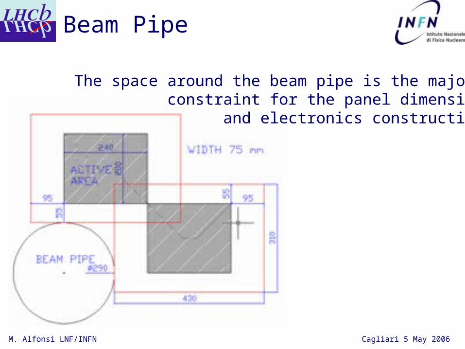
Beam Pipe
The space around the beam pipe is the major constraint for the panel dimension
and electronics construction

M. Alfonsi LNF/INFN Cagliari 5 May 2006
Honeycomb gas outlet
Cathode Panel
gas fitting
HV Panel
GEM Chamber side view
GEM Chamber top view
G1G2G3
PADs Panelgas inlet
7 mm
GEM Chamber Layout

M. Alfonsi LNF/INFN Cagliari 5 May 2006
Mechanical detector design
The cross section of a GEM Chamber Module
Pads PCBCathods PCB
bushing

M. Alfonsi LNF/INFN Cagliari 5 May 2006
G10 FRAMES

M. Alfonsi LNF/INFN Cagliari 5 May 2006
Frames layout Active area -Frame
3 mm - 7 mm
Frame Width 18 mm – 30 mm
Frame Thickness 1mm 2mm 3mm
6 holes for decoupling resistors
4 hole pins
Two glue roads(1 per size)
Glue road wide 6 mm
M. Alfonsi LNF/INFN Cagliari 5 May 2006
Position
Frame Thickness
Frame+glue
Thickness x
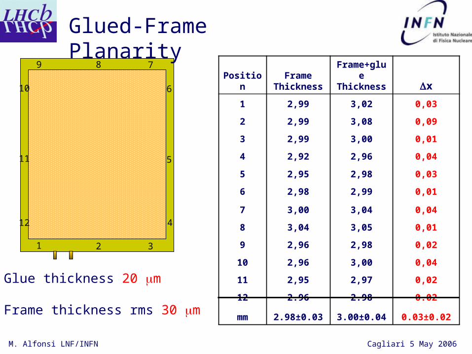
1 2,99 3,02 0,03
2 2,99 3,08 0,09
3 2,99 3,00 0,01
4 2,92 2,96 0,04
5 2,95 2,98 0,03
6 2,98 2,99 0,01
7 3,00 3,04 0,04
8 3,04 3,05 0,01
9 2,96 2,98 0,02
10 2,96 3,00 0,04
11 2,95 2,97 0,02
12 2.96 2.98 0.02
mm 2.98±0.03 3.00±0.04 0.03±0.02
1 2 3
4
5
6
789
10
11
12
Glued-Frame Planarity
Glue thickness 20 m
Frame thickness rms 30 m
M. Alfonsi LNF/INFN Cagliari 5 May 2006
GEM FOILS
M. Alfonsi LNF/INFN Cagliari 5 May 2006
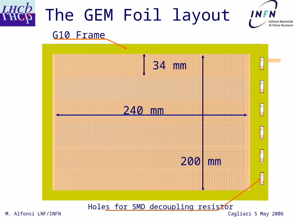
The GEM Foil layout
200 mm
240 mm
34 mm
Holes for SMD decoupling resistor
G10 Frame
M. Alfonsi LNF/INFN Cagliari 5 May 2006
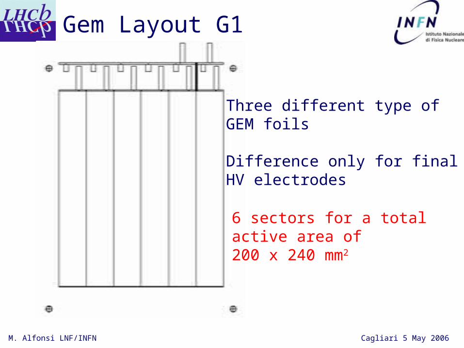
Gem Layout G1
Three different type of GEM foils
Difference only for final HV electrodes
6 sectors for a totalactive area of 200 x 240 mm2

M. Alfonsi LNF/INFN Cagliari 5 May 2006
Gem Layout G2
The sectors towards the cathode

M. Alfonsi LNF/INFN Cagliari 5 May 2006
Gem Layout G3
References for frame gluing
M. Alfonsi LNF/INFN Cagliari 5 May 2006
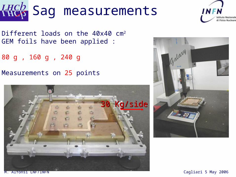
Sag measurements
Different loads on the 40x40 cm2
GEM foils have been applied :
80 g , 160 g , 240 g
Measurements on 25 points
30 Kg/side30 Kg/side
M. Alfonsi LNF/INFN Cagliari 5 May 2006
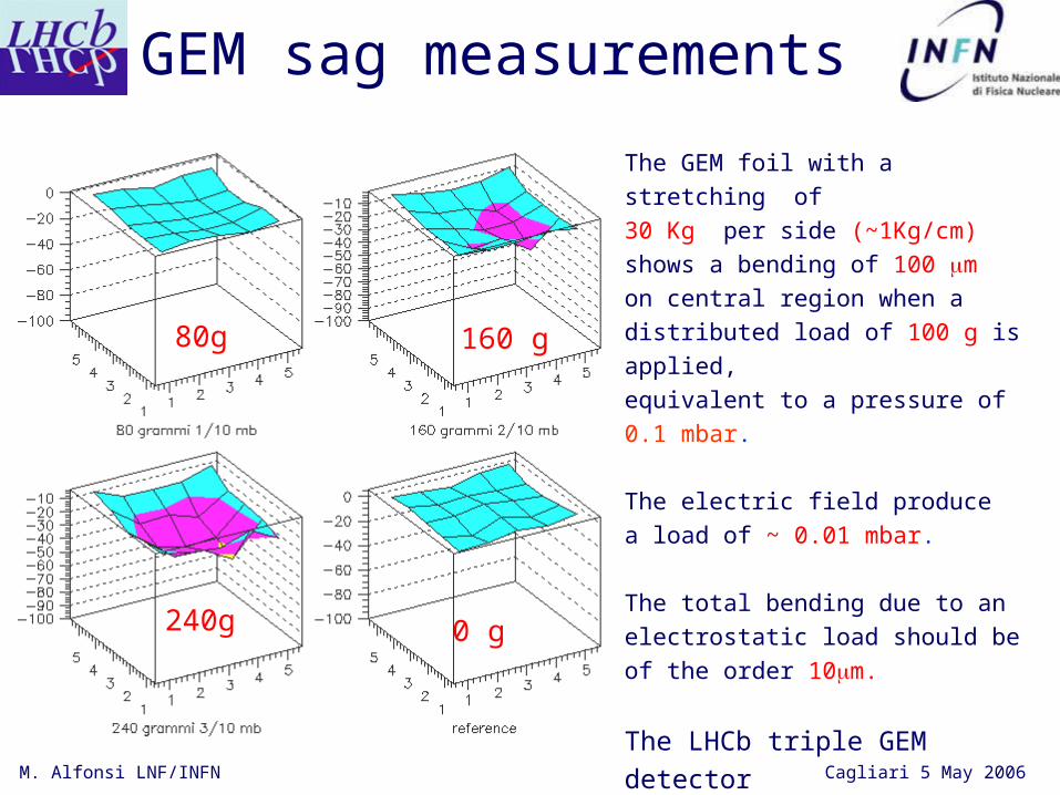
GEM sag measurements
The GEM foil with a stretching of 30 Kg per side (~1Kg/cm) shows a bending of 100 m
on central region when a distributed load of 100 g is applied, equivalent to a pressure of 0.1 mbar.
The electric field producea load of ~ 0.01 mbar.
The total bending due to an electrostatic load should be of the order 10m.
The LHCb triple GEM detector is built without spacers
80g 160 g
240g 0 g

M. Alfonsi LNF/INFN Cagliari 5 May 2006
Kapton Radiation Hardness
C= 251 pF C= 277 pF
C= 234 pF C= 266 pF
C = 32 pFd>= 120 m
After Aging
C = 26 pFd>= 94 m
Before Aging
After aging a sag increase of 30 m corresponding to3 m in normal condition after 4 LHCb years
Mechanical load 10 times the electrostatic pressure
M. Alfonsi LNF/INFN Cagliari 5 May 2006
HONEYCOMB PANELS
M. Alfonsi LNF/INFN Cagliari 5 May 2006
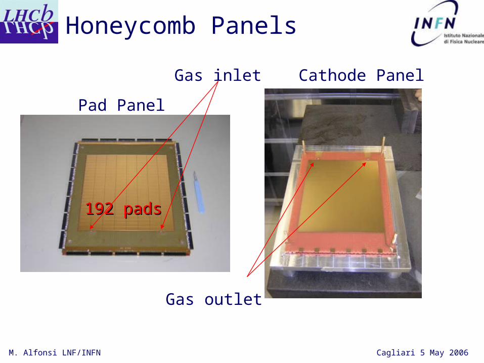
Honeycomb Panels
Pad Panel
Cathode Panel
192 pads192 pads
Gas outlet
Gas inlet
M. Alfonsi LNF/INFN Cagliari 5 May 2006
machined reference ALCOA plane
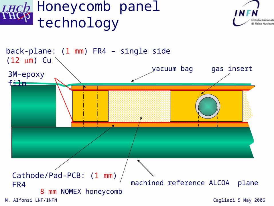
Honeycomb panel technology
back-plane: (1 mm) FR4 – single side (12 m) Cu
vacuum bag3M–epoxy film
Cathode/Pad-PCB: (1 mm) FR4
gas insert
8 mm NOMEX honeycomb
M. Alfonsi LNF/INFN Cagliari 5 May 2006
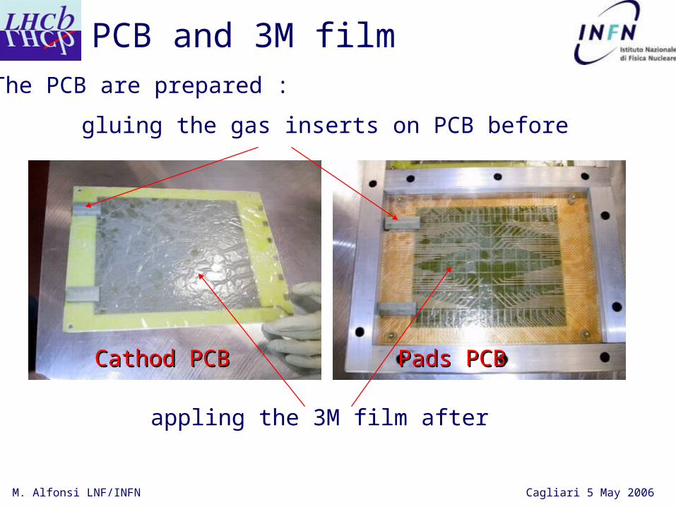
PCB and 3M filmThe PCB are prepared :
Cathod PCB Cathod PCB Pads PCBPads PCB
appling the 3M film after
gluing the gas inserts on PCB before

M. Alfonsi LNF/INFN Cagliari 5 May 2006
HoneycombThe honeycomb is placed on top of 3M film cutting the nomex in corrispondance of gas insert and pins
Gas insert :Stesalite and alluminum
Alcoa frames
Pins
The backplane with a 3M film is put on top of Nomexand everything is put in a oven at 80°C

M. Alfonsi LNF/INFN Cagliari 5 May 2006
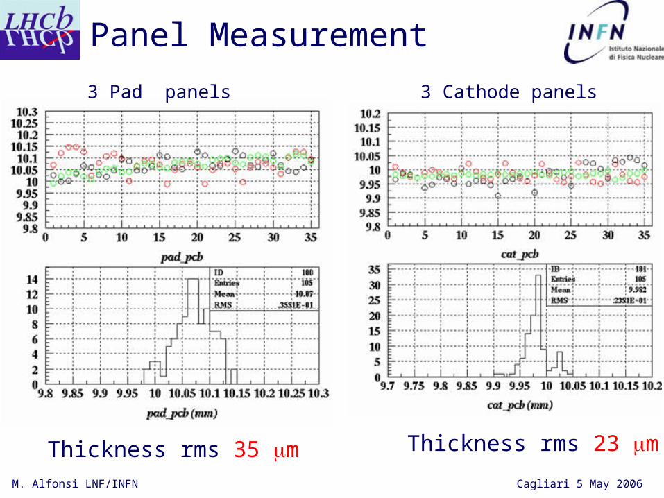
All panels will be checked for planarity with a 3-D machine at LNF. The measurements will be performed on a grid of 35 points.
3-D machine
5 10 15 20 25 30 35
4 9 14 19 24 29 34
3 8 13 18 23 28 33
2 7 12 17 22 27 32
1 6 11 16 21 26 31
Panel Planarity Measurements
Measurement points
M. Alfonsi LNF/INFN Cagliari 5 May 2006
3 Pad panels 3 Cathode panels
Panel Measurement
Thickness rms 35 m Thickness rms 23 m

M. Alfonsi LNF/INFN Cagliari 5 May 2006
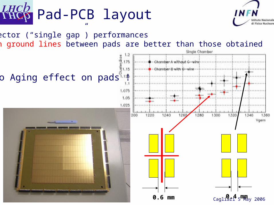
Pads layout Trigger sector
M. Alfonsi LNF/INFN Cagliari 5 May 2006
Detector (“single gap”) performances with ground lines between pads are better than those obtained
0.6 mm 0.4 mm
Pad-PCB layout
No Aging effect on pads !
M. Alfonsi LNF/INFN Cagliari 5 May 2006
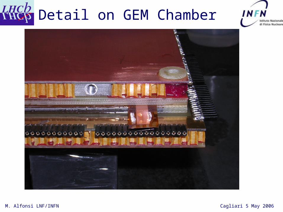
Detail on GEM Chamber

M. Alfonsi LNF/INFN Cagliari 5 May 2006
PAD -> 36 μm Cu 1.43 cm 0.25 % 2 mm G10 19.4 cm 1.03 %18 μm Cu 1.43 cm 0.13 % 1.42% X° 1 μm Ni 1.42 cm 0.007 % 0.15 μm Au 0.33 cm 0.005 %
GEM -> 10 μm Cu x3 1.43 cm 0.21 % 0.26% X°
50 μm kapton x3 28.6 cm 0.05 %
CAT -> 0.15 μm Au 0.33 cm 0.005 % 1 μm Ni 1.42 cm 0.007 %18 μm Cu 1.43 cm 0.13 % 1.42%
X° 2 mm G10 19.4 cm 1.03 %36 μm Cu 1.43 cm 0.25 %
3.10%Globally 3.1 x 2 (ch.s) = 6.2 % + 1% (FEE uniformely spread ) = 7.2%
Detector Material Budget