LVDS Source Synchronous 7:1 Serialization and ... Source Synchronous 7:1 Serialization and...
18
XAPP585 (v1.1.1) March 18, 2015 www.xilinx.com 1 Summary Xilinx 7 series FPGAs contain ISERDES and OSERDES primitives that make the design of serializer and deserializer circuits very straightforward and allows higher operation at speeds from 415 Mb/s to 1,200 Mb/s per line, when using per-bit deskew, depending on the family and speed grade used. Lower operation speeds use static data alignment. This application note describes how to use ISERDES and OSERDES efficiently in conjunction with the mixed-mode clock manager (MMCM) or phase-locked loop (PLL) for reception and transmission of 7:1 data using low-voltage differential signaling (LVDS) data transmission at speeds from 415 Mb/s to 1,200 Mb/s per line when using per-bit deskew, depending on the family and speed grade used. Download the Reference Design files for this application note from the Xilinx website. For detailed information about the design files, see Reference Design. Receiver Overview This type of 1:7 interface shown in Figure 1 (5-line interface shown) and requiring clock multiplication is widely used for video processing when passing data from one device to another in consumer devices such as televisions and Blu-ray players. One video channel is typically five LVDS data lines and one LVDS clock line. Modern televisions can use multiple channels, four or eight is typical, to ensure adequate video bandwidth. This application note provides a reference design for both single channel and multiple channel designs where the pixel clock frequency is the same for all channels, and only one clock multiplication element (MMCM or PLL) is needed for all channels so reducing the use of FPGA resources and making the designers choice of pinout much simpler. The macros are parameterizable for one or more channels, a single variable sets the number of channels to be generated, and another variable determines the number of LVDS data lines per channel. Channels can either be all in the same I/O bank of a 7 series FPGA or spread across different banks. It is advisable to keep all lines of the same channel in the same bank, but different channels can be in different banks provided the clocking elements are chosen appropriately. The input clock, generating internal clocks for all channels is the clock input of channel 0, this signal pair should therefore be placed on clock capable I/O pins. The clocks for the other channels are only used for framing purposes, and so can be placed on normal LVDS inputs if required. Application Note: 7 Series FPGAs XAPP585 (v1.1.1) March 18, 2015 LVDS Source Synchronous 7:1 Serialization and Deserialization Using Clock Multiplication Author: Nick Sawyer
Transcript of LVDS Source Synchronous 7:1 Serialization and ... Source Synchronous 7:1 Serialization and...

XAPP585 (v1.1.1) March 18, 2015 www.xilinx.com 1
SummaryXilinx 7 series FPGAs contain ISERDES and OSERDES primitives that make the design of serializer and deserializer circuits very straightforward and allows higher operation at speeds from 415 Mb/s to 1,200 Mb/s per line, when using per-bit deskew, depending on the family and speed grade used. Lower operation speeds use static data alignment. This application note describes how to use ISERDES and OSERDES efficiently in conjunction with the mixed-mode clock manager (MMCM) or phase-locked loop (PLL) for reception and transmission of 7:1 data using low-voltage differential signaling (LVDS) data transmission at speeds from 415 Mb/s to 1,200 Mb/s per line when using per-bit deskew, depending on the family and speed grade used.
Download the Reference Design files for this application note from the Xilinx website. For detailed information about the design f iles, see Reference Design.
Receiver OverviewThis type of 1:7 interface shown in Figure 1 (5-line interface shown) and requiring clock multiplication is widely used for video processing when passing data from one device to another in consumer devices such as televisions and Blu-ray players. One video channel is typically f ive LVDS data lines and one LVDS clock line. Modern televisions can use multiple channels, four or eight is typical, to ensure adequate video bandwidth.
This application note provides a reference design for both single channel and multiple channel designs where the pixel clock frequency is the same for all channels, and only one clock multiplication element (MMCM or PLL) is needed for all channels so reducing the use of FPGA resources and making the designers choice of pinout much simpler. The macros are parameterizable for one or more channels, a single variable sets the number of channels to be generated, and another variable determines the number of LVDS data lines per channel.
Channels can either be all in the same I/O bank of a 7 series FPGA or spread across different banks. It is advisable to keep all lines of the same channel in the same bank, but different channels can be in different banks provided the clocking elements are chosen appropriately.
The input clock, generating internal clocks for all channels is the clock input of channel 0, this signal pair should therefore be placed on clock capable I/O pins. The clocks for the other channels are only used for framing purposes, and so can be placed on normal LVDS inputs if required.
Application Note: 7 Series FPGAs
XAPP585 (v1.1.1) March 18, 2015
LVDS Source Synchronous 7:1 Serialization and Deserialization Using Clock MultiplicationAuthor: Nick Sawyer

ISERDES and OSERDES Guidelines
XAPP585 (v1.1.1) March 18, 2015 www.xilinx.com 2
Incoming data is optionally deskewed in real time on a per-pin basis using the input delays (IODELAYE2) present in the 7 series FPGAs, thereby allowing the designer to relax the PCB routing skew requirements and providing tighter timing margins.
ISERDES and OSERDES GuidelinesEach I/O logic tile in the 7 series FPGAs contains an 8-bit ISERDES and an 8-bit OSERDES. The ISERDES and OSERDES from two adjacent blocks (master and slave) can be cascaded to give a 10-bit or 14-bit block. This gives the possibility of ISERDES input ratios from 1:2 to 1:8 inclusive, 1:10 and 1:14 for single data rate (SDR) operation, and 1:2, 1:4, 1:6, 1:8, 1:10 and 1:14 for double data rate (DDR) operation. The OSERDES has output ratios from 2:1 to 8:1 inclusive, 10:1 and 14:1 for SDR operation, 2:1, 4:1, 6:1, 8:1, 10:1 and 14:1 for DDR I/O clocks.
Cascading the ISERDES or OSERDES blocks is not a problem when differential signaling standard is used, as these standards use the two I/O logic tiles (master and slave) associated with the ISERDES and OSERDES registers, thus using two ISERDES or OSERDES is effectively free. Differential signaling is typically the standard for 7:1 applications in flat-panel displays and cameras.
SDR techniques should be used when the bit rate required is less than the maximum clock supported by the chosen clock network in the required device and speed grade. Above this speed DDR techniques can be used, and the maximum bit rate achievable in that case is limited by the maximum output frequency of the PLL or MMCM. The advantage of using SDR techniques is that the general interconnect logic required is much less and any duty cycle distortion in the clock is irrelevant. Because there is no native support for 7:1 DDR in the ISERDES and the OSERDES, a distributed RAM gearbox must be used to enable the function. This gearbox takes in 4-bit wide data from the ISERDES at a clock frequency equal to 1/4 of the sampling clock, and outputs 7-bit wide data at a frequency equal to the sampling clock divided by 7, i.e., the originally received pixel clock.
X-Ref Target - Figure 1
Figure 1: Data Stream Using a Low-Speed Forwarded Clock with 7:1 SerDes Factor
Received 1:7 Data
Line 0
Line 1
Line 2
Line 3
Line 4
Received ClockXAPP585_01_042912
D0 D5 D10 D15 D20 D30D25
D1 D6 D11 D16 D21 D31D26
D2 D7 D12 D17 D22 D32D27
D3 D8 D13 D18 D23 D33D28
D4 D9 D14 D19 D24 D34D29

Clocking Guidelines
XAPP585 (v1.1.1) March 18, 2015 www.xilinx.com 3
Clocking GuidelinesThe MMCM can drive BUFIO, BUFR, BUFH, and BUFG clock networks. The PLL can drive only BUFH and BUFG clock networks.
The maximum frequencies for the available clock networks for the 7 series FPGA speed grades are shown in Table 1. These specif ications should be confirmed with the latest version of the Artix-7 FPGAs Data Sheet: DC and AC Switching Characteristics (DS181) [Ref 1], Kintex-7 FPGAs Data Sheet: DC and AC Switching Characteristics (DS182) [Ref 2], and Virtex-7 FPGAs Data Sheet: DC and AC Switching Characteristics (DS183) [Ref 3] for completeness. However, it usual that this sort of application is used in a cost sensitive product, and therefore requires use of the slowest speed grade available. Testing has currently been limited to 1,200 Mb/s per line.
The various design variations described are summarized with regards to maximum operating frequency in Table 2 and Table 3.
Only the slowest speed grade (-1) is shown in Table 2 and Table 3.
Other speed grade maximum speeds can be ascertained from the respective 7 series FPGAs data sheet. The SDR clocking requires two clock buffers and DDR clocking requires three. Any combinations of clock buffers not listed are either unsupported by the silicon or are not recommended solutions.
Table 1: Global Clock and PLL/MMCM Specifications in 7 Series FPGAs
FPGA SpeedGrade
Global Clock Network Maximum
(BUFG)
I/O Clock Network Maximum (BUFIO)
Regional Clock Network Maximum
(BUFR)
Horizontal Clock Network Maximum
(BUFH)
Artix®-7 -1 464 MHz 600 MHz 315 MHz 464 MHz
Artix-7 -2 550 MHz 680 MHz 375 MHz 550 MHz
Kintex®-7 -1 625 MHz 710 MHz 450 MHz 625 MHz
Kintex-7 -2 710 MHz 800 MHz 540 MHz 710 MHz
Virtex®-7 -1 625 MHz 710 MHz 450 MHz 625 MHz
Virtex-7 -2 710 MHz 800 MHz 540 MHz 710 MHz
Table 2: Maximum Bit Rate Limits for SDR Design Variations
CLK (x7) + CLKDIV (x1) Single or Multiple Interfaces in One Bank (Common Pixel Clock)
Multiple Interfaces in More Than One Bank (Common Pixel Clock) PLL or MMCM
BUFG + BUFG
Artix-7 FPGAs: 464 Mb/s Artix-7 FPGAs: 464 Mb/s
PLL/MMCMKintex-7 FPGAs: 625 Mb/s Kintex-7 FPGAs: 625 Mb/s
Virtex-7 FPGAs: 625 Mb/s Virtex-7 FPGAs: 625 Mb/s
BUFIO + BUFR
Artix-7 FPGAs: 600 Mb/s
Not Possible MMCM onlyKintex-7 FPGAs: 710 Mb/s
Virtex-7 FPGAs: 710 Mb/s

Introduction to 1:7 Deserialization and Data Reception
XAPP585 (v1.1.1) March 18, 2015 www.xilinx.com 4
Introduction to 1:7 Deserialization and Data ReceptionThe data stream is a multiple (x7) of the rate of the incoming clock and the clock signal is itself used as a framing signal for the received data. There are seven changes in the state of the data lines during one clock period. A widely used example is the 7:1 interface used in cameras, flat-panel televisions, and monitors. In this use case, the received clock is multiplied by 7 in a PLL or MMCM, and the resultant high-speed clock is passed to the ISERDES logic via a global buffer (BUFG), an I/O buffer (BUFIO), or a horizontal clock buffer (BUFH). The clock buffers can be used in either SDR or DDR mode.
Input data is presented to the ISERDES via an IODELAYE2 element that has been trained by the state machine to be as close as possible to ½ unit interval (UI) delay relative to the sample clock. This is achieved by using the incoming clock as a training reference. Framing data
BUFH + BUFH
Artix-7 FPGAs: 464 Mb/s
Not Possible PLL/MMCMKintex-7 FPGAs: 625 Mb/s
Virtex-7 FPGAs: 625 Mb/s
BUFR + BUFR
Artix-7 FPGAs: 315 Mb/s
Not Possible MMCM onlyKintex-7 FPGAs: 450 Mb/s
Virtex-7 FPGAs: 450 Mb/s
Table 2: Maximum Bit Rate Limits for SDR Design Variations (Cont’d)
CLK (x7) + CLKDIV (x1) Single or Multiple Interfaces in One Bank (Common Pixel Clock)
Multiple Interfaces in More Than One Bank (Common Pixel Clock) PLL or MMCM
Table 3: Maximum Bit Rate Limits for DDR Design Variations
CLK (x7) + CLKDIV (x7/4) + PCLK (x1)
Single or Multiple Interfaces in One Bank (Common Pixel Clock)
Multiple Interfaces in More Than One Bank (Common Pixel Clock) PLL or MMCM
BUFG + BUFG + BUFG
Artix-7 FPGAs: 928 Mb/s Artix-7 FPGAs: 928 Mb/s
PLL/MMCMKintex-7 FPGAs: 1,200 Mb/s Kintex-7 FPGAs: 1,200 Mb/s
Virtex-7 FPGAs: 1,200 Mb/s Virtex-7 FPGAs: 1,200 Mb/s
BUFIO + BUFR + BUFG
Artix-7 FPGAs: 1,200 Mb/s
Not Possible MMCM onlyKintex-7 FPGAs: 1,200 Mb/s
Virtex-7 FPGAs: 1,200 Mb/s
BUFH + BUFH + BUFG
Artix-7 FPGAs: 928 Mb/s
Not Possible PLL/MMCMKintex-7 FPGAs: 1,200 Mb/s
Virtex-7 FPGAs: 1,200 Mb/s
BUFIO + BUFR + BUFR
Artix-7 FPGAs: 1,200 Mb/s
Not Possible MMCM onlyKintex-7 FPGAs: 1,200 Mb/s
Virtex-7 FPGAs: 1,200 Mb/s
BUFH + BUFH + BUFH
Artix-7 FPGAs: 928 Mb/s
Not Possible PLL/MMCMKintex-7 FPGAs: 1,200 Mb/s
Virtex-7 FPGAs: 1,200 Mb/s

Introduction to 1:7 Deserialization and Data Reception
XAPP585 (v1.1.1) March 18, 2015 www.xilinx.com 5
obtained from the incoming pixel clock is also used together with the Bitslip feature of the ISERDES to generate parallel data that is in the correct word relationship to the originally transmitted data as shown in Figure 1. Finally, this deserialized parallel data is presented to the general interconnect logic at the speed of the original incoming clock.
There are two design considerations here. When using an SDR sampling clock, the ISERDES is used directly in a 1:7 mode. The only clock element combinations supported by the ISERDES are two BUFGs, two BUFHs or a BUFIO and a BUFR. The advantage of using a BUFG is that the parallel data is then available on a clock that covers the whole device. With a BUFR or a BUFH, the data is available on a clock that only covers the current clock region. When multiple channels running at the same pixel clock rate are to be received they can be placed in the same I/O bank and all clock options are available, or they can be placed in different banks and only BUFG clocking can be used.
When using a DDR sampling clock, the ISERDES is used in a 1:4 mode and the full 1:7 mode is emulated using a distributed RAM based gearbox. This approach requires three clock domains. The sampling clock, the sampling clock divided by 4, and the sampling clock divided by 7 which is equal to the original input pixel clock. These clock elements are shown in Table 3. As with the SDR case, when multiple channels running at the same pixel clock rate are to be received, they can be placed in the same I/O bank and all clock options are available, or they can be placed in different banks and only BUFG networks for all clocking are used.
In either case, when a PLL rather than an MMCM is used for clock multiplication, only BUFH or BUFG clocking is available because these buffers are the only type that the PLL can access.
Basic Data ReceptionThe topology for this mechanism is very straight forward. The receiver clock is multiplied as required in the PLL or MMCM to generate an internal SDR or DDR receiver clock. In the 7:1 video use case example, the received pixel clock is multiplied by 7 for the SDR designs or by 3.5 for the DDR designs. Different clock networks can be chosen for data reception depending on the mode and topology used. For either SDR or DDR designs, if a single or multiple channel design is used where all the input pins are in the same bank, then the preferred solution is to use the BUFIO and BUFR as clocks for the SerDes. These clocks can be replaced with either two BUFH clock networks or two BUFG networks. In the case where inputs span more than one bank, then two BUFG clock networks is the only solution currently proposed. DDR data reception also requires one more intermediate clock, which can be either a BUFH or a BUFG clock network. The choice is determined by the fanout of the received clock required.
SDR Data Reception without Per-Bit DeskewThe SDR design without deskew uses the ISERDES primitives in 1:7 mode directly, so the received 7-bits per data line are available synchronous to the clock network chosen, either BUFR, BUFH, or BUFG. As shown in Figure 2, the incoming clock is routed to the PLL or MMCM as previously described, it is also routed to an IODELAYE2 element that is under control of a state machine and from there to an ISERDES primitive. The incoming data lines are also routed to an IODELAYE2 element and then to a ISERDES primitive configured for 1:7 data reception.

Introduction to 1:7 Deserialization and Data Reception
XAPP585 (v1.1.1) March 18, 2015 www.xilinx.com 6
The clock delay is initially set to a value corresponding to the number of taps corresponding to the current bit rate, which is set by a 16-bit input to the macro. For example 0560 would correspond to 560 Mb/s. A 5-bit value from 01h to 1Fh is generated internally to the macro to correspond to the bit rate programmed. This 5-bit value equals the number of taps equivalent to the current UI time. The 0560 input, for example, would give an output of 17h as 17h (23d) x the nominal tap delay value of 78 ps = 1,794 ps = 557 Mb/s. The 5-bit value is not precise by definition, but any rounding is accounted for in the timing analysis.
After the receiver PLL or MMCM indicates it is locked, the state machine slowly decrements the clock delay from its initial value until a change in received 7-bit clock data is seen. This corresponds to an edge on the clock being detected and the current value of the clock delay is then increased or decreased by a half UI according to its current position, so that the delay is nominally in the center of the data eye with respect to the clock that has been multiplied by the PLL or MMCM. This value is also transferred to the delay input on the associated data lines, so that the data lines are also being sampled at their midpoint.
One possible sequence of events would be:
1. Set clock delay to 17h.
2. Decrement clock delay until a change is seen on the clock data inputs, let's say this is seen at a delay value of 05h.
3. Add or subtract ½ bit period delay to the delay line. One half of 17h is rounded to 0Bh. 05h – 0Bh is negative and is not appropriate. Therefore, 05h + 0Bh = 10h is used as the final value for the clock delay line.
4. This value of 10h is also used for the delay lines in the data inputs of the associated channel, normally four or f ive data inputs per channel. The number of data inputs is programmable via a parameter on the macro.
Finally, input data from the clock line is tested for a known pattern, normally 1100001 or 1100011, to ensure that the received parallel data is in the correct relationship to the received clock (see Figure 1). If the received pattern is not correct, a Bitslip command is issued to effectively move all input clock and data bits by one position as described in 7 Series FPGAs SelectIO Resources User Guide (UG471) [Ref 4]. Bitslip commands are repeated up to seven times until the correct pattern is seen, and the parallel received data is therefore correctly framed.
No further timing adjustment takes place. The PLL or MMCM maintains the clock in its current position as V and T vary ensuring correct data reception. This method assumes that the clock and data lines in the channel are well aligned on the PCB. A full timing analysis is given in the Receiver Timing Considerations.
The macro can also account for further channels. The number of channels is programmable via a parameter on the macro. The incoming clock on these further channels is not used for frequency multiplication. The multiplied clock from channel 0 is the only receiver clock used. The incoming clock on for example channel 1 is, however, used as an input to the state machine for channel 1, and alignment proceeds as described above. Again it is assumed that to use this method, the clock and data lines within a channel are well aligned, but there is no requirement that individual channels be aligned with each other, only that they operate at an identical frequency.

Introduction to 1:7 Deserialization and Data Reception
XAPP585 (v1.1.1) March 18, 2015 www.xilinx.com 7
DDR Data Reception without Per-Bit DeskewThe DDR design without deskew uses the ISERDES primitives in 1:4 mode, and then data is transferred from 4-bit wide at clock frequency divided by 4 to 7-bits wide at the pixel clock frequency via a distributed RAM based gearbox directly. The received 7-bits per data line are available synchronous to the clock network chosen, either BUFR, BUFH, or BUFG. A diagram of the DDR receiver is shown in Figure 3.
With the exception of the addition of the gearbox and one extra clock from the PLL or MMCM, the operation of the DDR case is identical to the SDR case outlined SDR Data Reception without Per-Bit Deskew.
X-Ref Target - Figure 2
Figure 2: Data Reception Using SDR Techniques without Per-Bit Deskew
LVDS CLOCK PChannel 0
LVDS CLOCK NChannel 0
LVDS DATA PChannel 0
LVDS DATA NChannel 0
ISERDESIDELAY
n_x_serdes_1_to_7_mmcm_idelay_sdr.v/vhd
ISERDES IDELAY
BUFx
BITSLIP Calibration &bitslip State
Machine
ParametersN = Number of Channels
SAMPL_CLOCK = Receiverclock Buffer TypePIXEL_CLOCK = Pixel Clock Buffer Type
USE_PLL = Use PLL or MMCMMMCM_MODE = Multiplication Factor for PLL/MMCM
DIFF_TERM = Enable/disable Internal TerminationCLKIN_PERIOD = Input Clock Period
HIGH_PERFORMANCE_MODE = TRUE or FALSE
Signals :enable_phase_detector = ‘0’bit_rate_value = X“bitrate”, e.g., X“1050”
D Data Lines
ReceiveClock
BUFxPLL/
MMCM
ReceivePixel Clock
LVDS DATA PChannel N-1
LVDS DATA NChannel N-1
ISERDES IDELAYClock Line
LVDS DATA PChannel N-1
LVDS DATA NChannel N-1
ISERDES IDELAYD Data Lines
BITSLIP
Channel 0 DataD*7 bits
Channel N-1 DataD*7 bits
7
7
7
7
Calibration &bitslip State
Machine
XAPP585_02_031815

Introduction to 1:7 Deserialization and Data Reception
XAPP585 (v1.1.1) March 18, 2015 www.xilinx.com 8
Once again it is possible to use multiple receive channels, but the assumption is that data and clock lines are well aligned within a channel, but no requirement for alignment between channels.
SDR Data Reception with Per-Bit DeskewData reception is similar to the standard SDR case in that the correct clock delay is determined and passed to the IODELAYE2s on the data lines. The input data lines are also routed to a second IODELAYE2 and a second ISERDES primitive as shown in Figure 6. The second delay and ISERDES are free because the input standard is LVDS requiring two input pins.
The initial delay of the master data delay is set to be nominally in the middle of the eye as before. The slave delay is set to be a half-bit period different (earlier or later). As a result, two samples are taken of the incoming data line, separated by a half-bit period.
X-Ref Target - Figure 3
Figure 3: Data Reception Using DDR Techniques without Per-Bit Deskew
LVDS CLOCK PChannel 0
LVDS CLOCK NChannel 0
LVDS DATA PChannel 0
LVDS DATA NChannel 0
ISERDESIDELAY
n_x_serdes_1_to_7_mmcm_idelay_ddr.v/vhd
ISERDES IDELAY
BUFx
BUFx
BITSLIP Gearbox,Calibration &bitslip State
Machine
Gearbox
Gearbox
Gearbox,Calibration &bitslip State
Machine
ParametersN = Number of Channels
SAMPL_CLOCK = Receiverclock Buffer TypeINTER_CLOCK = Intermediate Clock Buffer Type
PIXEL_CLOCK = Pixel Clock Buffer TypeUSE_PLL = Use PLL or MMCM
MMCM_MODE = Multiplication Factor for PLL/MMCMDIFF_TERM = Enable/disable Internal Termination
CLKIN_PERIOD = Input Clock PeriodHIGH_PERFORMANCE_MODE = TRUE or FALSE
Signals :enable_phase_detector = ‘0’bit_rate_value = X“bitrate”, e.g., X“0560”
D Data Lines
ReceiveClock
BUFx
PLL/MMCM
ReceivePixel Clock
LVDS DATA PChannel N-1
LVDS DATA NChannel N-1
ISERDES IDELAYClock Line
LVDS DATA PChannel N-1
LVDS DATA NChannel N-1
ISERDES IDELAYD Data Lines
BITSLIP
Channel 0 DataD*7 bits
Channel N-1 DataD*7 bits
7 4
4 7
4
4
XAPP585_03_121514

Introduction to 1:7 Deserialization and Data Reception
XAPP585 (v1.1.1) March 18, 2015 www.xilinx.com 9
The algorithm used to then determine the correct sampling delay is as follows. If the two samples taken a half-bit period apart (following a transition) are the same, then the sampling point is too late and the input delays need to be reduced by one tap (Figure 4). If the two samples taken (following a transition) are different, then the sampling point is too early and the input delays need to be increased by one tap (Figure 5). This mechanism requires changes in the incoming data. If the data line is a static 0 or static 1, the delays remain at the initial value determined by calibration to the incoming clock until data line transitions arrive.
Because it is impossible to do this the comparison in real time synchronous to the sampling clock, the parallel 7-bit data is used, i.e., two 7-bit samples per input line are required.
There are two pathological cases possible with this algorithm: One is when a delay wraps around towards zero and the other when the delay wraps around away from zero. In either case data corruption occurs, with either a bit being received twice, or not at all. The general interconnect logic includes registers and multiplexers to detect either situation and inserts pipeline stages appropriately to ensure that data corruption never occurs.
The disadvantage is that this approach requires an amount of general interconnect logic to implement, the advantage is that each input line is individually deskewed in real time, while correct data reception is guaranteed. This allows sources of skew such as PCB routing, pin delays, and transmitter pin variation to be removed from the timing analysis.
The deskew algorithm works with any amount of bit variation in either direction, but due to the nature of video interfaces where the parallel word is required to synchronized to the incoming pixel clock pattern, it is recommended that the input and clock line skew is kept within plus or minus one-fourth UI on a per-channel basis. The circuit still works outside this range, but further user logic possibly might be required to perform word deskew. The receiver block diagram for this case is shown in Figure 6.
X-Ref Target - Figure 4
Figure 4: Data Sampling – Delay Is Too LongX-Ref Target - Figure 5
Figure 5: Data Sampling – Delay Is Too Short
1/2 bit Period
Slave Sample Master Sample
XAPP585_04_042912
1/2 bit Period
Slave Sample Master Sample
XAPP585_05_042912

Introduction to 1:7 Deserialization and Data Reception
XAPP585 (v1.1.1) March 18, 2015 www.xilinx.com 10
DDR Data Reception with Per Bit-DeskewThe f inal data reception case covered is DDR techniques with per-bit deskew. Data is received as in the standard DDR case, i.e., 1:4 ISERDES configuration and an intermediate clock with a gearbox, but the slave ISERDES is now also used. This is also configured as 1:4, and there are now two IODELAYE2 set to values a half-bit period apart, one for each ISERDES.
The deskew mechanism works as before with the exception that the sample data is the 4-bit data taken direct from the master and slave ISERDES. The resultant output is once again moved to the pixel clock domain using a 4-bit to 7-bit gearbox as shown in Figure 7.
X-Ref Target - Figure 6
Figure 6: Data Reception Using SDR Techniques with Per-Bit Deskew
LVDS CLOCK PChannel 0
LVDS CLOCK NChannel 0
LVDS DATA PChannel 0
LVDS DATA NChannel 0
ISERDESIDELAY
n_x_serdes_1_to_7_mmcm_idelay_sdr.v/vhd
ISERDES IDELAY
ISERDES IDELAY
BUFx
BITSLIP Calibration &bitslip State
Machine
DeskewControl
ParametersN = Number of Channels
SAMPL_CLOCK = Receiverclock Buffer TypePIXEL_CLOCK = Pixel Clock Buffer Type
USE_PLL = Use PLL or MMCMMMCM_MODE = Multiplication Factor for PLL/MMCM
DIFF_TERM = Enable/disable Internal TerminationCLKIN_PERIOD = Input Clock Period
HIGH_PERFORMANCE_MODE = TRUE or FALSE
Signals :enable_phase_detector = ‘1’bit_rate_value = X“bitrate”, e.g., X“1050”
D Data Lines
ReceiveClock
BUFxPLL/
MMCM
ReceivePixel Clock
LVDS DATA PChannel N-1
LVDS DATA NChannel N-1
ISERDES IDELAYClock Line
LVDS DATA PChannel N-1
LVDS DATA NChannel N-1
D Data Lines
BITSLIP
Channel 0 DataD*7 bits
Channel N-1 DataD*7 bits
7
7
7
ISERDES IDELAY
ISERDES IDELAYDeskewControl 7
7
7
7
7
Calibration &bitslip State
Machine
XAPP585_06_121514

Introduction to 1:7 Deserialization and Data Reception
XAPP585 (v1.1.1) March 18, 2015 www.xilinx.com 11
Minimum Data Rate ConsiderationsThe data capture mechanism is dependent on the IODELAYE2 block. This block has 31 delays of nominally 78 ps and so the minimum capture frequency = 78 x 31 = 2,418 ps = 415 Mb/s. Any bit rate below this value could result in no edges at all being found. In the case where no edge is found, the clock calibration circuit sets the IDELAY to half max tap setting and stops. By setting this to half the value, you have at least 1,170 ps of margin on either side of the sampling clock. Data reception below 415 Mb/s (59.28 MHz pixel clock) therefore automatically disables per-bit deskew (if enabled). If an edge is found in the delay line, then the f inal delay is statically set to be this value, ± 10h taps. If no edge is found, then the delay line is set to be 10h taps. In either case, the delay is set to be at least 10h taps away from the edge of the eye, which is acceptable at these lower bit rates.
This lower limit does obviously not apply to the transmitter logic where no training is required.
X-Ref Target - Figure 7
Figure 7: Data Reception Using DDR Techniques with Per-Bit Deskew
LVDS CLOCK PChannel 0
LVDS CLOCK NChannel 0
LVDS DATA PChannel 0
LVDS DATA NChannel 0
ISERDESIDELAY
n_x_serdes_1_to_7_mmcm_idelay_ddr.v/vhd
BUFx
BUFx
BITSLIP Gearbox,Calibration &bitslip State
Machine
Gearbox,Calibration &bitslip State
Machine
ParametersN = Number of Channels
SAMPL_CLOCK = Receiverclock Buffer TypeINTER_CLOCK = Intermediate Clock Buffer Type
PIXEL_CLOCK = Pixel Clock Buffer TypeUSE_PLL = Use PLL or MMCM
MMCM_MODE = Multiplication Factor for PLL/MMCMDIFF_TERM = Enable/disable Internal Termination
CLKIN_PERIOD = Input Clock PeriodHIGH_PERFORMANCE_MODE = TRUE or FALSE
Signals :enable_phase_detector = ‘1’bit_rate_value = X“bitrate”, eg X“0560”
D Data Lines
ReceiveClock
BUFx
PLL/MMCM
ReceivePixel Clock
LVDS DATA PChannel N-1
LVDS DATA NChannel N-1
ISERDES IDELAYClock Line
LVDS DATA PChannel N-1
LVDS DATA NChannel N-1
D Data Lines
BITSLIP
Channel N-1 DataD*7 bits
4
4
XAPP585_07_121514
ISERDES IDELAY
ISERDES IDELAY
Gearbox&
DeskewControl
Channel 0 DataD*7 bits 7
4
4
ISERDES IDELAY
ISERDES IDELAY
Gearbox&
DeskewControl
7
4
4
Introduction to Serialization and Data Transmission
XAPP585 (v1.1.1) March 18, 2015 www.xilinx.com 12
Introduction to Serialization and Data TransmissionThe required output forwarded clock and data stream change state at the same time, and can therefore be generated from the same transmit clock. An example of this is the 7:1 interface used in cameras and flat-panel televisions and monitors as shown in Figure 8.
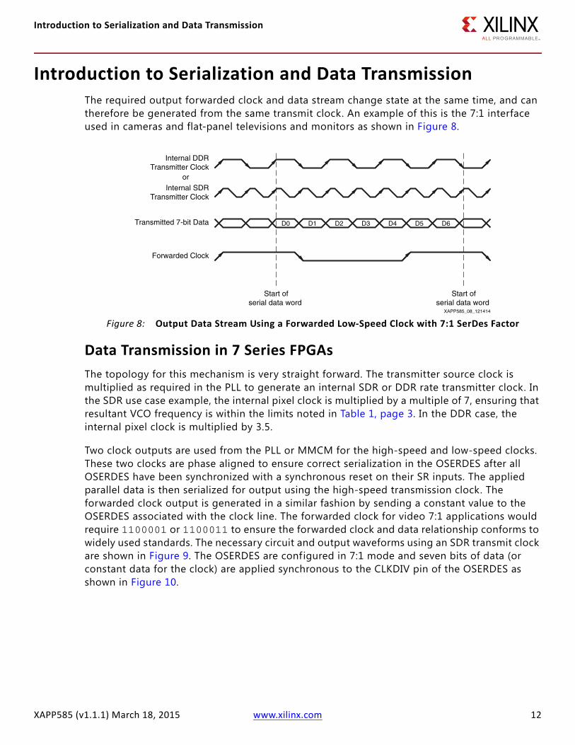
Data Transmission in 7 Series FPGAsThe topology for this mechanism is very straight forward. The transmitter source clock is multiplied as required in the PLL to generate an internal SDR or DDR rate transmitter clock. In the SDR use case example, the internal pixel clock is multiplied by a multiple of 7, ensuring that resultant VCO frequency is within the limits noted in Table 1, page 3. In the DDR case, the internal pixel clock is multiplied by 3.5.
Two clock outputs are used from the PLL or MMCM for the high-speed and low-speed clocks. These two clocks are phase aligned to ensure correct serialization in the OSERDES after all OSERDES have been synchronized with a synchronous reset on their SR inputs. The applied parallel data is then serialized for output using the high-speed transmission clock. The forwarded clock output is generated in a similar fashion by sending a constant value to the OSERDES associated with the clock line. The forwarded clock for video 7:1 applications would require 1100001 or 1100011 to ensure the forwarded clock and data relationship conforms to widely used standards. The necessary circuit and output waveforms using an SDR transmit clock are shown in Figure 9. The OSERDES are configured in 7:1 mode and seven bits of data (or constant data for the clock) are applied synchronous to the CLKDIV pin of the OSERDES as shown in Figure 10.
X-Ref Target - Figure 8
Figure 8: Output Data Stream Using a Forwarded Low-Speed Clock with 7:1 SerDes FactorXAPP585_08_121414
Internal SDRTransmitter Clock
Transmitted 7-bit Data
Forwarded Clock
Start ofserial data word
D0 D1 D2 D3 D4 D5 D6
Start ofserial data word
Internal DDRTransmitter Clock
or
Introduction to Serialization and Data Transmission
XAPP585 (v1.1.1) March 18, 2015 www.xilinx.com 13
Often where one FPGA is performing both data reception and data transmission of the 7:1 standard, the PLL or MMCM is shared between the transmitter and receiver. The same PLL and clock networks can then be used for both data reception and transmission.
DDR ConsiderationsThe topology for the DDR mechanism is slightly more complex than for the SDR case. The OSERDES cannot perform 7:1 serialization in DDR mode, but can be configured to use 14:1 (when cascaded) in DDR mode. The transmitter source clock is multiplied by 3.5 in the PLL/MMCM to generate an internal DDR transmitter clock and a pixel clock at the same frequency as the input. In addition, a third clock is required that is running at half the speed of the pixel clock. This clock is used for the CLKDIV inputs of the OSERDES, and is 1/14 of the high-speed transmission clock. Data needs to be presented to the OSERDES 14 bits at a time synchronous to this slow, third clock.
Internal data at pixel clock rate is moved to this slower third clock via a simple gearbox shown in Figure 10. Data is input to the gearbox 7-bits wide at pixel clock rates, and output at 14-bits wide at half the pixel clock rate for direct connection to the OSERDES as shown in Figure 10.
X-Ref Target - Figure 9
Figure 9: Data Transmission Using SDR TechniquesXAPP585_09_121514
LVDS CLOCK P
LVDS CLOCK N
clock_generator_pll_7_to_1_diff_sdr.v/vhd
PLL/MMCM
BUFx
ParametersTX_CLOCK = Transmission Clock Buffer Type
PIXEL_CLOCK = Pixel Clock Buffer TypeUSE_PLL = Use PLL or MMCM
MMCM_MODE = Multiplication Factor for PLL/MMCMDIFF_TERM = Enable/disable Internal Termination
CLKIN_PERIOD = Input Clock Period
SDR MASTEROSERDES
n_x_serdes_7_to_1_diff_sdr.v/vhd
Parameters :D = Number of Data Lines per Channel
N = N umber of Channels
D*N*7-bit TransmitterData from Logic
D Data Lines– Channel 0
Forwarded Clock– Channel 0
System (Pixel) Clock
High Speed DDR Clock
BUFx
SDR MASTEROSERDES
SDR MASTEROSERDES
D Data Lines– Channel N-1
Forwarded Clock– Channel N-1
SDR MASTEROSERDES
7-bit Constant forClock Generation

Introduction to Serialization and Data Transmission
XAPP585 (v1.1.1) March 18, 2015 www.xilinx.com 14
Receiver Timing ConsiderationsSeveral sources of uncertainty need to be taken into account for the receiver. These sources should be subtracted from the bit period to analyze whether the design meets the designer’s requirements. To aid in this, an Excel spreadsheet is included with the design ZIP f ile to allow rapid analysis. A screen shot is shown in Figure 11. After the user enters the parameters for their particular design in the white cells of the spreadsheet, the calculated remaining receiver margin and receiver skew margin (RSKM) are displayed in either green or red indicating whether the margin is positive or negative.
Sources of uncertainty include:
• PLL/MMCM jitter. The number for this is available via the clocking wizard.
• Per-bit deskew accuracy. When using per-bit deskew this number is ±2 delay taps, including any rounding errors. When not using per-bit deskew, this number is half the length of the
X-Ref Target - Figure 10
Figure 10: Data Transmission Using DDR TechniquesXAPP585_10_031815
LVDS CLOCK P
LVDS CLOCK N
clock_generator_pll_7_to_1_diff_ddr.v/vhd
PLL/MMCM
BUFx
ParametersTX_CLOCK = Transmission Clock Buffer Type
INTER_CLOCK = Intermediate Clock Buffer TypePIXEL_CLOCK = Pixel Clock Buffer Type
USE_PLL = Use PLL or MMCMMMCM_MODE = Multiplication Factor for PLL/MMCM
DIFF_TERM = Enable/disable Internal TerminationCLKIN_PERIOD = Input Clock Period
DDR MASTEROSERDES
Gearbox7 to 14
Gearbox7 to 14
n_x_serdes_7_to_1_diff_ddr.v/vhd
Parameters :D = Number of Data Lines per Channel
N = Number of Channels
D*N*7-bit TransmitterData from Logic
D Data Lines– Channel 0
Forwarded Clock– Channel 0
System (Pixel) Clock
High Speed DDR ClockGearboxClock
BUFx
BUFx
DDR MASTEROSERDES
DDR MASTEROSERDES
D Data Lines– Channel N-1
Forwarded Clock– Channel N-1
DDR MASTEROSERDES
7-bit Constant forClock Generation
DDR SLAVEOSERDES
DDR SLAVEOSERDES
DDR SLAVEOSERDES
DDR SLAVEOSERDES

Introduction to Serialization and Data Transmission
XAPP585 (v1.1.1) March 18, 2015 www.xilinx.com 15
IODELAYE2 element. In either case, this number includes any clock skew between the master and slave IODELAYE2 elements, and also any difference in setup and hold timing between these two elements. The IODELAYE2 elements require a reference clock of either 200 MHz or 300 MHz to operate correctly. More information on the IODELAYE2 and its associated IDELAYCTRL control block is available in 7 Series FPGAs SelectIO Resources User Guide (UG471) [Ref 4]. Increasing the reference clock frequency to 300 MHz improves the receiver margin at the cost of increasing the minimum per-bit deskew operating bit rate to 641 Mb/s.
• Pattern dependent jitter in the delay line. This is normally 9 ps per tap, but can be reduced to 5 ps per tap when using the HIGH_PERFORMANCE mode of the IODELAYE2 element. The number of taps used is calculated in the spreadsheet.
• Sampling clock duty cycle distortion. This is only meaningful when using DDR techniques and varies with the type of buffer chosen for the receiver sampling clock.
• Transmitter skew, pcb skew, package skew. These are all cancelled out when using per-bit deskew designs, but should be included when not using per-bit deskew.
X-Ref Target - Figure 11
Figure 11: Screen Shot of the Included XLS Receiver Margin Calculation
XAPP585_11_060512

Reference Design
XAPP585 (v1.1.1) March 18, 2015 www.xilinx.com 16
Reference DesignDownload the Reference Design f iles for this application note from the Xilinx website. The files are available in both Verilog and VHDL.
The name of the appropriate file is included in the figures for different methodologies shown throughout this document. Also included are example top level f iles and example timing constraints for the 7:1 interface used in flat-panel displays and cameras.
Each of the SDR data input and output modules is parameterizable for interface bus width (number of input or output pins per interface) and number of interfaces using common clocking that are required. The files included are:
• clock_generator_pll_7_to_1_diff_sdr.v/vhd
• n_x_serdes_7_to_1_diff_sdr.v/vhd
• n_x_serdes_1_to_7_mmcm_idelay_sdr.v/vhd
Each of the DDR data input and output modules is parameterizable for input width (number of input or output pins per interface) and the number of interfaces using common clocking that are required. The files included are:
• clock_generator_pll_7_to_1_diff_ddr.v/vhd
• n_x_serdes_7_to_1_diff_ddr.v/vhd
• n_x_serdes_1_to_7_mmcm_idelay_ddr.v/vhd
Table 4 shows the reference design matrix.
Table 4: Reference Design Matrix
Parameter Description
General Xilinx
Developer name Xilinx
Target devices 7 series FPGAs
Source code provided Yes
Source code format Verilog, VHDL
Design uses code/IP from an existing reference design, application note, third party, CORE Generator™ tool No
Simulation
Functional simulation performed Yes
Timing simulation performed No
Testbench used for functional and timing simulations provided Yes
Testbench format Verilog, VHDL
Simulator software used ISIM
SPICE/IBIS simulations No

Conclusion
XAPP585 (v1.1.1) March 18, 2015 www.xilinx.com 17
ConclusionThe 7 series FPGAs perform in a wide variety of applications requiring serialization and deserialization factors of 7:1 at speeds from 415 Mb/s to 1,200 Mb/s per line with per-bit deskew enabled, depending on the family and speed grade used.
References1. Artix-7 FPGAs Data Sheet: DC and AC Switching Characteristics (DS181)
2. Kintex-7 FPGAs Data Sheet: DC and AC Switching Characteristics (DS182)
3. Virtex-7 FPGAs Data Sheet: DC and AC Switching Characteristics (DS183)
4. 7 Series FPGAs SelectIO Resources User Guide (UG471)
5. 7 Series FPGAs Overview Data Sheet (DS180)
Implementation
Synthesis software tools used XST 13.4
Implementation software tools used ISE® Design Suite 13.4
Static timing analysis performed Yes
Hardware Verification
Hardware verified Yes
Hardware platform used for verification KC705 or VC707 with FMC-X107
Table 4: Reference Design Matrix (Cont’d)
Parameter Description
Table 5: Device Utilization
Design File PLL orMMCM
ClockBuffers Slices ISERDES OSERDES
clock_generator_pll_7_to_1_diff_sdr.v/vhd 1 2 0 0 0
n_x_serdes_7_to_1_diff_sdr.v/vhd 0 0 12 0 1 per line
clock_generator_pll_7_to_1_diff_ddr.v/vhd 1 3 0 0 0
n_x_serdes_7_to_1_diff_ddr.v/vhd 0 0 12 0 2 per line
n_x_serdes_1_to_7_mmcm_idelay_sdr.v/vhd
Per-bit deskew disabled1 2
~8per line
1per line
0
n_x_serdes_1_to_7_mmcm_idelay_ddr.v/vhd
Per-bit deskew disabled1 3
~17per line
2per line
0
n_x_serdes_1_to_7_mmcm_idelay_sdr.v/vhd
Per-bit deskew enabled1 2
~36per line
2per line
0
n_x_serdes_1_to_7_mmcm_idelay_ddr.v/vhd
Per-bit deskew enabled1 3
~45per line
2per line
0

Revision History
XAPP585 (v1.1.1) March 18, 2015 www.xilinx.com 18
Revision HistoryThe following table shows the revision history for this document.
Please Read: Important Legal NoticesThe information disclosed to you hereunder (the “Materials”) is provided solely for the selection and use of Xilinx products. To the maximum extent permitted by applicable law: (1) Materials are made available "AS IS" and with all faults, Xilinx hereby DISCLAIMS ALL WARRANTIES AND CONDITIONS, EXPRESS, IMPLIED, OR STATUTORY, INCLUDING BUT NOT LIMITED TO WARRANTIES OF MERCHANTABILITY, NON-INFRINGEMENT, OR FITNESS FOR ANY PARTICULAR PURPOSE; and (2) Xilinx shall not be liable (whether in contract or tort, including negligence, or under any other theory of liability) for any loss or damage of any kind or nature related to, arising under, or in connection with, the Materials (including your use of the Materials), including for any direct, indirect, special, incidental, or consequential loss or damage (including loss of data, profits, goodwill, or any type of loss or damage suffered as a result of any action brought by a third party) even if such damage or loss was reasonably foreseeable or Xilinx had been advised of the possibility of the same. Xilinx assumes no obligation to correct any errors contained in the Materials or to notify you of updates to the Materials or to product specifications. You may not reproduce, modify, distribute, or publicly display the Materials without prior written consent. Certain products are subject to the terms and conditions of Xilinx’s limited warranty, please refer to Xilinx’s Terms of Sale which can be viewed at http://www.xilinx.com/legal.htm#tos; IP cores may be subject to warranty and support terms contained in a license issued to you by Xilinx. Xilinx products are not designed or intended to be fail-safe or for use in any application requiring fail-safe performance; you assume sole risk and liability for use of Xilinx products in such critical applications, please refer to Xilinx’s Terms of Sale which can be viewed at http://www.xilinx.com/legal.htm#tos.Automotive Applications DisclaimerXILINX PRODUCTS ARE NOT DESIGNED OR INTENDED TO BE FAIL-SAFE, OR FOR USE IN ANY APPLICATION REQUIRING FAIL-SAFE PERFORMANCE, SUCH AS APPLICATIONS RELATED TO: (I) THE DEPLOYMENT OF AIRBAGS, (II) CONTROL OF A VEHICLE, UNLESS THERE IS A FAIL-SAFE OR REDUNDANCY FEATURE (WHICH DOES NOT INCLUDE USE OF SOFTWARE IN THE XILINX DEVICE TO IMPLEMENT THE REDUNDANCY) AND A WARNING SIGNAL UPON FAILURE TO THE OPERATOR, OR (III) USES THAT COULD LEAD TO DEATH OR PERSONAL INJURY. CUSTOMER ASSUMES THE SOLE RISK AND LIABILITY OF ANY USE OF XILINX PRODUCTS IN SUCH APPLICATIONS.© Copyright 2012–2015 Xilinx, Inc. Xilinx, the Xilinx logo, Artix, ISE, Kintex, Spartan, Virtex, Vivado, Zynq, and other designated brands included herein are trademarks of Xilinx in the United States and other countries. All other trademarks are the property of their respective owners.
Date Version Revision
06/27/2012 1.0 Initial Xilinx release.
02/20/2015 1.1 In Figure 2 and Figure 3, enable_phase_detector was changed to 0. The heading of Figure 6 changed to n_x_serdes_1_to_7_mmcm_idelay_sdr.v/vhd. In Figure 7, enable_phase_detector was changed to 1. Updated Minimum Data Rate Considerations, page 11. In the last two rows of Table 5, the design f iles changed to per-bit deskew enabled. Reference design ZIP file was updated.
03/18/2015 1.1.1 Updated three typos in Figure 2 and Figure 10.