
LTM8028 - 36VIN, UltraFast, Low Output Noise 5A …cds.linear.com/docs/en/datasheet/8028fb.pdf ·...
24
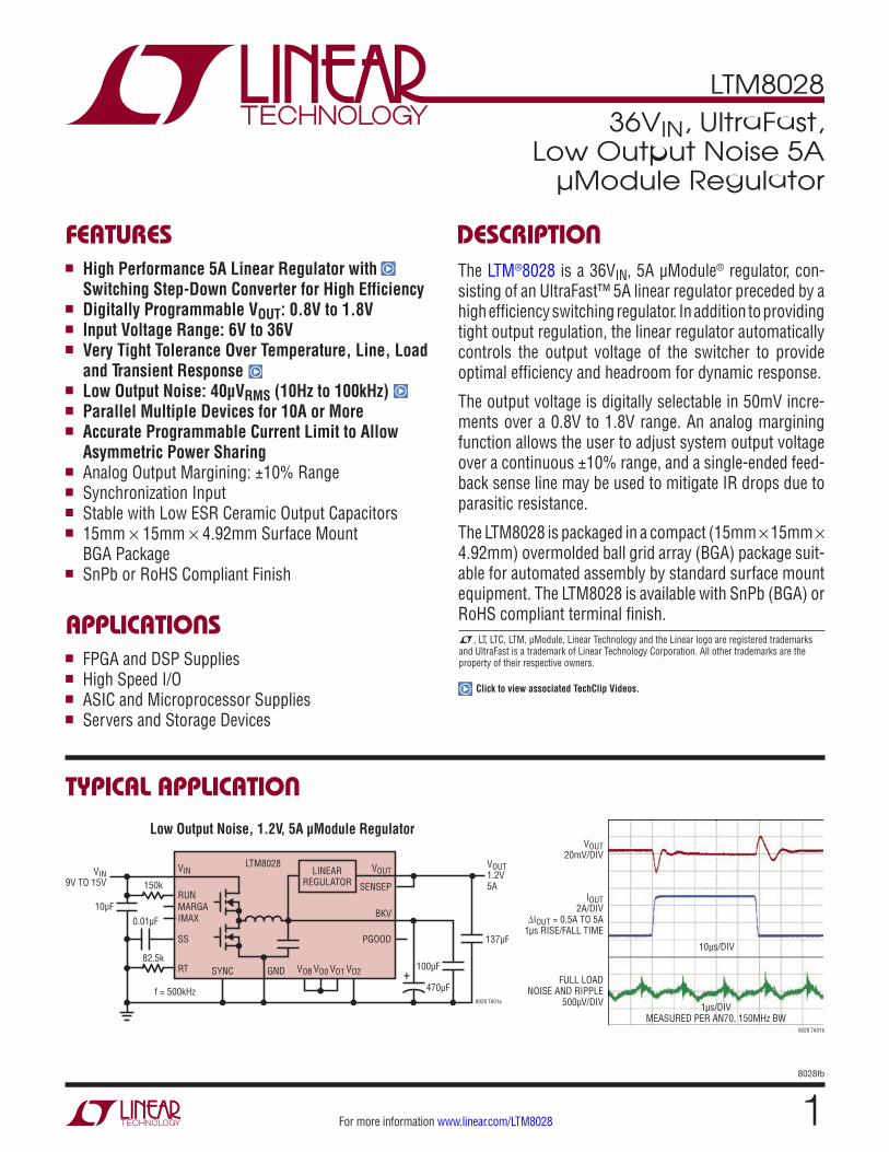
LTM8028 1 8028fb For more information www.linear.com/LTM8028 TYPICAL APPLICATION FEATURES DESCRIPTION 36V IN , UltraFast, Low Output Noise 5A µModule Regulator The LTM ® 8028 is a 36V IN , 5A µModule ® regulator, con- sisting of an UltraFast™ 5A linear regulator preceded by a high efficiency switching regulator. In addition to providing tight output regulation, the linear regulator automatically controls the output voltage of the switcher to provide optimal efficiency and headroom for dynamic response. The output voltage is digitally selectable in 50mV incre- ments over a 0.8V to 1.8V range. An analog margining function allows the user to adjust system output voltage over a continuous ±10% range, and a single-ended feed- back sense line may be used to mitigate IR drops due to parasitic resistance. The LTM8028 is packaged in a compact (15mm × 15mm × 4.92mm) overmolded ball grid array (BGA) package suit- able for automated assembly by standard surface mount equipment. The LTM8028 is available with SnPb (BGA) or RoHS compliant terminal finish. APPLICATIONS n High Performance 5A Linear Regulator with Switching Step-Down Converter for High Efficiency n Digitally Programmable V OUT : 0.8V to 1.8V n Input Voltage Range: 6V to 36V n Very Tight Tolerance Over Temperature, Line, Load and Transient Response n Low Output Noise: 40μV RMS (10Hz to 100kHz) n Parallel Multiple Devices for 10A or More n Accurate Programmable Current Limit to Allow Asymmetric Power Sharing n Analog Output Margining: ±10% Range n Synchronization Input n Stable with Low ESR Ceramic Output Capacitors n 15mm × 15mm × 4.92mm Surface Mount BGA Package n SnPb or RoHS Compliant Finish n FPGA and DSP Supplies n High Speed I/O n ASIC and Microprocessor Supplies n Servers and Storage Devices L, LT, LTC, LTM, µModule, Linear Technology and the Linear logo are registered trademarks and UltraFast is a trademark of Linear Technology Corporation. All other trademarks are the property of their respective owners. + LINEAR REGULATOR V IN V OUT SENSEP BKV RUN 150k V IN 9V TO 15V 82.5k f = 500kHz 0.01μF MARGA IMAX SS PGOOD 100μF RT GND V OB V O0 V O1 V O2 470μF 8028 TA01a 137μF V OUT 1.2V 5A SYNC LTM8028 10μF V OUT 20mV/DIV FULL LOAD NOISE AND RIPPLE 500μV/DIV I OUT 2A/DIV ΔI OUT = 0.5A TO 5A 1μs RISE/FALL TIME 10μs/DIV 8028 TA01b 1μs/DIV MEASURED PER AN70, 150MHz BW Low Output Noise, 1.2V, 5A µModule Regulator Click to view associated TechClip Videos.
Transcript of LTM8028 - 36VIN, UltraFast, Low Output Noise 5A …cds.linear.com/docs/en/datasheet/8028fb.pdf ·...
LTM8028
18028fb
For more information www.linear.com/LTM8028
Typical applicaTion
FeaTures DescripTion
36VIN, UltraFast, Low Output Noise 5A
µModule Regulator
The LTM®8028 is a 36VIN, 5A µModule® regulator, con-sisting of an UltraFast™ 5A linear regulator preceded by a high efficiency switching regulator. In addition to providing tight output regulation, the linear regulator automatically controls the output voltage of the switcher to provide optimal efficiency and headroom for dynamic response.
The output voltage is digitally selectable in 50mV incre-ments over a 0.8V to 1.8V range. An analog margining function allows the user to adjust system output voltage over a continuous ±10% range, and a single-ended feed-back sense line may be used to mitigate IR drops due to parasitic resistance.
The LTM8028 is packaged in a compact (15mm × 15mm × 4.92mm) overmolded ball grid array (BGA) package suit-able for automated assembly by standard surface mount equipment. The LTM8028 is available with SnPb (BGA) or RoHS compliant terminal finish. applicaTions
n High Performance 5A Linear Regulator with Switching Step-Down Converter for High Efficiency
n Digitally Programmable VOUT: 0.8V to 1.8Vn Input Voltage Range: 6V to 36Vn Very Tight Tolerance Over Temperature, Line, Load
and Transient Responsen Low Output Noise: 40μVRMS (10Hz to 100kHz)n Parallel Multiple Devices for 10A or More n Accurate Programmable Current Limit to Allow
Asymmetric Power Sharingn Analog Output Margining: ±10% Rangen Synchronization Inputn Stable with Low ESR Ceramic Output Capacitors n 15mm × 15mm × 4.92mm Surface Mount
BGA Packagen SnPb or RoHS Compliant Finish
n FPGA and DSP Suppliesn High Speed I/On ASIC and Microprocessor Suppliesn Servers and Storage Devices
L, LT, LTC, LTM, µModule, Linear Technology and the Linear logo are registered trademarks and UltraFast is a trademark of Linear Technology Corporation. All other trademarks are the property of their respective owners.
+
LINEARREGULATOR
VIN VOUT
SENSEP
BKV
RUN150k
VIN9V TO 15V
82.5k
f = 500kHz
0.01µFMARGAIMAX
SS PGOOD
100µFRT GND VOB VO0 VO1 VO2
470µF8028 TA01a
137µF
VOUT1.2V5A
SYNC
LTM8028
10µF
VOUT20mV/DIV
FULL LOADNOISE AND RIPPLE
500µV/DIV
IOUT2A/DIV
∆IOUT = 0.5A TO 5A1µs RISE/FALL TIME
10µs/DIV
8028 TA01b
1µs/DIVMEASURED PER AN70, 150MHz BW
Low Output Noise, 1.2V, 5A µModule Regulator
Click to view associated TechClip Videos.
LTM8028
28028fb
For more information www.linear.com/LTM8028
absoluTe MaxiMuM raTings
VIN ............................................................................40VVOUT ............................................................................3VRUN, SS, SYNC ..........................................................6VCurrent Into RUN ..................................................100μAVOB, VO0, VO1, VO2, TEST, PGOOD, SENSEP, MARGA ...........................................4VRT, BKV, IMAX .............................................................3VMaximum Operating Junction Temperature(Note 2) ................................................................. 125°CPeak Solder Reflow Body Temperature ................. 245°CMaximum Storage Temperature ............................ 125°C
(Notes 1, 4)
elecTrical characTerisTics The l denotes the specifications which apply over the full internal operating temperature range, otherwise specifications are at TA = 25°C. VIN = 12V, RUN = 3V unless otherwise noted. (Note 2)
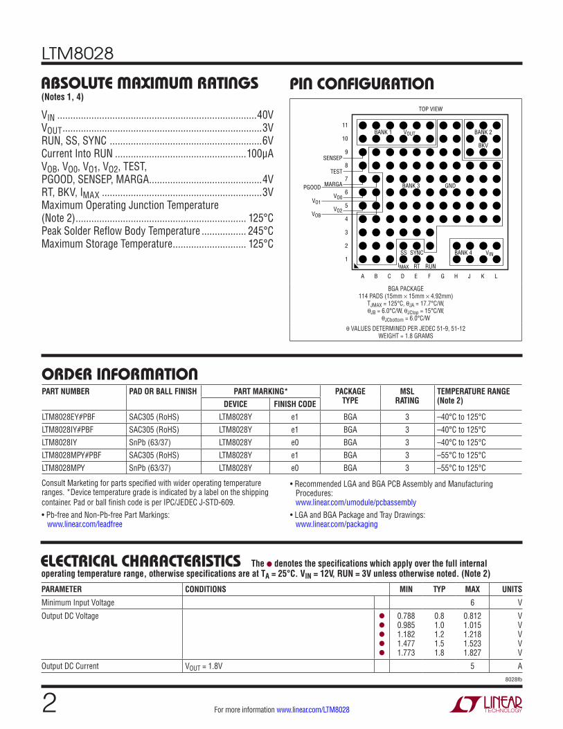
pin conFiguraTion
A
1
2
3
4
5
6
7
8
9
10
11
B C D E F
TOP VIEW
BANK 1 BANK 2
BANK 3
SENSEP
BANK 4
RUNRT
SS SYNC
IMAX
VIN
GND
BKV
VOUT
G H J K L
TEST
MARGAPGOODVO0VO1VO2VOB
BGA PACKAGE114 PADS (15mm × 15mm × 4.92mm)
TJMAX = 125°C, θJA = 17.7°C/W,θJB = 6.0°C/W, θJCtop = 15°C/W,
θJCbottom = 6.0°C/W
θ VALUES DETERMINED PER JEDEC 51-9, 51-12WEIGHT = 1.8 GRAMS
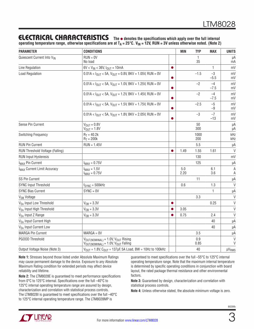
PARAMETER CONDITIONS MIN TYP MAX UNITS
Minimum Input Voltage 6 V
Output DC Voltage l
l
l
l
l
0.788 0.985 1.182 1.477 1.773
0.8 1.0 1.2 1.5 1.8
0.812 1.015 1.218 1.523 1.827
V V V V V
Output DC Current VOUT = 1.8V 5 A
orDer inForMaTionPART NUMBER PAD OR BALL FINISH PART MARKING* PACKAGE
TYPEMSL
RATINGTEMPERATURE RANGE (Note 2)DEVICE FINISH CODE
LTM8028EY#PBF SAC305 (RoHS) LTM8028Y e1 BGA 3 –40°C to 125°CLTM8028IY#PBF SAC305 (RoHS) LTM8028Y e1 BGA 3 –40°C to 125°CLTM8028IY SnPb (63/37) LTM8028Y e0 BGA 3 –40°C to 125°CLTM8028MPY#PBF SAC305 (RoHS) LTM8028Y e1 BGA 3 –55°C to 125°CLTM8028MPY SnPb (63/37) LTM8028Y e0 BGA 3 –55°C to 125°C
Consult Marketing for parts specified with wider operating temperature ranges. *Device temperature grade is indicated by a label on the shipping container. Pad or ball finish code is per IPC/JEDEC J-STD-609.• Pb-free and Non-Pb-free Part Markings:
www.linear.com/leadfree
• Recommended LGA and BGA PCB Assembly and Manufacturing Procedures: www.linear.com/umodule/pcbassembly
• LGA and BGA Package and Tray Drawings: www.linear.com/packaging
LTM8028
38028fb
For more information www.linear.com/LTM8028
elecTrical characTerisTics
Note 1: Stresses beyond those listed under Absolute Maximum Ratings may cause permanent damage to the device. Exposure to any Absolute Maximum Rating condition for extended periods may affect device reliability and lifetime.Note 2: The LTM8028E is guaranteed to meet performance specifications from 0°C to 125°C internal. Specifications over the full –40°C to 125°C internal operating temperature range are assured by design, characterization and correlation with statistical process controls. The LTM8028I is guaranteed to meet specifications over the full –40°C to 125°C internal operating temperature range. The LTM8028MP is
The l denotes the specifications which apply over the full internal operating temperature range, otherwise specifications are at TA = 25°C. VIN = 12V, RUN = 3V unless otherwise noted. (Note 2)
PARAMETER CONDITIONS MIN TYP MAX UNITS
Quiescent Current Into VIN RUN = 0V No load
1 35
µA mA
Line Regulation 6V < VIN < 36V, IOUT = 10mA l 1 mV
Load Regulation 0.01A < IOUT < 5A, VOUT = 0.8V, BKV = 1.05V, RUN = 0V
l
–1.5 –3 –5.5
mV mV
0.01A < IOUT < 5A, VOUT = 1.0V, BKV = 1.25V, RUN = 0V
l
–2 –4 –7.5
mV mV
0.01A < IOUT < 5A, VOUT = 1.2V, BKV = 1.45V, RUN = 0V
l
–2 –4 –7.5
mV mV
0.01A < IOUT < 5A, VOUT = 1.5V, BKV = 1.75V, RUN = 0V
l
–2.5 –5 –9
mV mV
0.01A < IOUT < 5A, VOUT = 1.8V, BKV = 2.05V, RUN = 0V
l
–3 –7 –13
mV mV
Sense Pin Current VOUT = 0.8V VOUT = 1.8V
50 300
µA µA
Switching Frequency RT = 40.2k RT = 200k
1000 200
kHz kHz
RUN Pin Current RUN = 1.45V 5.5 µA
RUN Threshold Voltage (Falling) l 1.49 1.55 1.61 V
RUN Input Hysteresis 130 mV
IMAX Pin Current IMAX = 0.75V 125 µA
IMAX Current Limit Accuracy IMAX = 1.5V IMAX = 0.75V
5.0 2.20
6.1 3.6
A A
SS Pin Current 11 µA
SYNC Input Threshold fSYNC = 500kHz 0.6 1.3 V
SYNC Bias Current SYNC = 0V 1 µA
VOB Voltage 3.3 V
VOx Input Low Threshold VOB = 3.3V l 0.25 V
VOx Input High Threshold VOB = 3.3V l 3.05 V
VOx Input Z Range VOB = 3.3V l 0.75 2.4 V
VOx Input Current High 40 µA
VOx Input Current Low 40 µA
MARGA Pin Current MARGA = 0V 3.5 μA
PGOOD Threshold VOUT(NOMINAL) = 1.0V, VOUT Rising VOUT(NOMINAL) = 1.0V, VOUT Falling
0.9 0.85
V V
Output Voltage Noise (Note 3) VOUT = 1.8V, COUT = 137µF, 5A Load, BW = 10Hz to 100kHz 40 µVRMS
guaranteed to meet specifications over the full –55°C to 125°C internal operating temperature range. Note that the maximum internal temperature is determined by specific operating conditions in conjunction with board layout, the rated package thermal resistance and other environmental factors.Note 3: Guaranteed by design, characterization and correlation with statistical process controls.Note 4: Unless otherwise stated, the absolute minimum voltage is zero.

LTM8028
48028fb
For more information www.linear.com/LTM8028
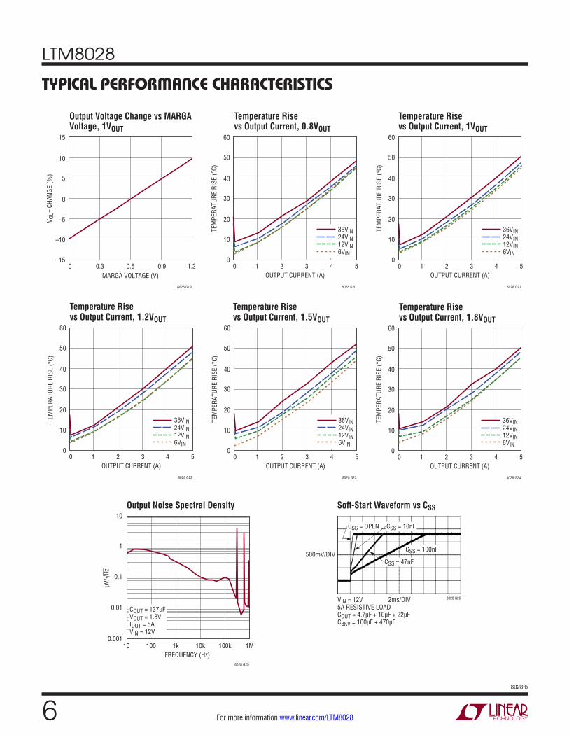
Typical perForMance characTerisTics
Power Loss vs Output Current, 1.5VOUT
Power Loss vs Output Current, 1.8VOUT
Input Current vs Output Current, 0.8VOUT
Input Current vs Output Current, 1VOUT
Input Current vs Output Current, 1.2VOUT
Input Current vs Output Current, 1.5VOUT
Power Loss vs Output Current, 0.8VOUT
Power Loss vs Output Current, 1VOUT
Power Loss vs Output Current, 1.2VOUT
OUTPUT CURRENT (A)0
POW
ER L
OSS
(W)
3
4
5
4
8028 G01
2
1
01 2 3 5
36VIN24VIN12VIN6VIN
OUTPUT CURRENT (A)0
POW
ER L
OSS
(W)
3
4
5
4
8028 G02
2
1
01 2 3 5
36VIN24VIN12VIN6VIN
OUTPUT CURRENT (A)0
POW
ER L
OSS
(W)
3
4
5
4
8028 G03
2
1
01 2 3 5
36VIN24VIN12VIN6VIN
OUTPUT CURRENT (A)0
POW
ER L
OSS
(W)
3
4
5
4
8028 G04
2
1
01 2 3 5
36VIN24VIN12VIN6VIN
OUTPUT CURRENT (A)0
POW
ER L
OSS
(W)
3
4
5
4
8028 G05
2
1
01 2 3 5
36VIN24VIN12VIN6VIN
OUTPUT CURRENT (A)0
1000
1200
1400
4
8026 G06
800
600
1 2 3 5
400
200
0
INPU
T CU
RREN
T (m
A)
6VIN12VIN24VIN36VIN
OUTPUT CURRENT (A)0
INPU
T CU
RREN
T (m
A)
600
800
1000
3 5
8028 G07
400
200
01 2 4
1200
1400
16006VIN12VIN24VIN36VIN
OUTPUT CURRENT (A)0
0
INPU
T CU
RREN
T (m
A)
200
600
800
1000
2 4 5
1800
8028 G08
400
1 3
1200
1400
16006VIN12VIN24VIN36VIN
OUTPUT CURRENT (A)0
INPU
T CU
RREN
T (m
A)
1200
1600
2000
4
8028 G09
800
400
1000
1400
1800
600
200
01 2 3 5
6VIN12VIN24VIN36VIN

LTM8028
58028fb
For more information www.linear.com/LTM8028
Typical perForMance characTerisTics
Transient Response, Demo Board, 1V
Transient Response, Demo Board, 1.2V
Transient Response, Demo Board, 1.5V
Transient Response, Demo Board, 1.8V Output Noise, 1.8VOUT
Output Current vs IMAX Voltage, 12VIN
Input Current vs Output Current, 1.8VOUT
Input Current vs Input Voltage, Output Shorted
Output Current vs Input Voltage, Output Shorted
OUTPUT CURRENT (A)0
INPU
T CU
RREN
T (m
A)
1500
2000
2500
4
8028 G10
1000
500
01 2 3 5
6VIN12VIN24VIN36VIN
INPUT VOLTAGE (V)0
0
INPU
T CU
RREN
T (m
A)
200
400
600
800
1000
1200
10 20 30 40
8038 G11
INPUT VOLTAGE (V)0
5.0
OUTP
UT C
URRE
NT (A
)
5.2
5.4
5.6
5.8
6.0
6 12 18 24
8028 G12
30 36
IMAX VOLTAGE (V)0
1
0
OUTP
UT C
URRE
NT (A
)
2
3
4
5
6
0.5 1.0 1.5 2.0
8028 G18
VOUT20mV/DIV
IOUT2A/DIV∆IOUT
0.5A TO 5A1µs
RISE/FALLTIME
10µs/DIVCOUT = 100µF + 22µF + 10µF + 4.7µF
8028 G13
VOUT20mV/DIV
IOUT2A/DIV∆IOUT
0.5A TO 5A1µs
RISE/FALLTIME
10µs/DIVCOUT = 100µF + 22µF + 10µF + 4.7µF
8028 G14
VOUT20mV/DIV
IOUT2A/DIV∆IOUT
0.5A TO 5A1µs
RISE/FALLTIME
10µs/DIVCOUT = 100µF + 22µF + 10µF + 4.7µF
8028 G15
VOUT20mV/DIV
IOUT2A/DIV∆IOUT
0.5A TO 5A1µs
RISE/FALLTIME 20µs/DIV
COUT = 100µF + 22µF + 10µF + 4.7µF
8028 G16
500µV/DIV
1µs/DIVMEASURED WITH HP461A AMPLIFIER (150MHz BW) AT J5 BNC CONNECTORON DC1738 DEMO BOARDfSW = 500kHzCOUT = 137µF5A LOAD
8028 G17
LTM8028
68028fb
For more information www.linear.com/LTM8028
Typical perForMance characTerisTics
Temperature Rise vs Output Current, 1.2VOUT
Temperature Rise vs Output Current, 1.5VOUT
Temperature Rise vs Output Current, 1.8VOUT
Output Noise Spectral Density Soft-Start Waveform vs CSS
Output Voltage Change vs MARGA Voltage, 1VOUT
Temperature Rise vs Output Current, 0.8VOUT
Temperature Rise vs Output Current, 1VOUT
MARGA VOLTAGE (V)0
–10
–15
V OUT
CHA
NGE
(%)
–5
0
5
10
15
0.3 0.6 0.9 1.2
8028 G19
OUTPUT CURRENT (A)0
0
TEM
PERA
TURE
RIS
E (°
C)
10
20
30
40
50
60
1 2 3 4
8028 G20
5
36VIN24VIN12VIN6VIN
OUTPUT CURRENT (A)0
0
TEM
PERA
TURE
RIS
E (°
C)
10
20
30
40
50
60
1 2 3 4
8028 G21
5
36VIN24VIN12VIN6VIN
OUTPUT CURRENT (A)0
0
TEM
PERA
TURE
RIS
E (°
C)
10
20
30
40
50
60
1 2 3 4
8028 G22
5
36VIN24VIN12VIN6VIN
OUTPUT CURRENT (A)0
0
TEM
PERA
TURE
RIS
E (°
C)
10
20
30
40
50
60
1 2 3 4
8028 G23
5
36VIN24VIN12VIN6VIN
OUTPUT CURRENT (A)0
0
TEM
PERA
TURE
RIS
E (°
C)
10
20
30
40
50
60
1 2 3 4
8028 G24
5
36VIN24VIN12VIN6VIN
FREQUENCY (Hz)
0.01
µV/√Hz 0.1
1
10
10 100 1k 10k 100k 1M0.001
8028 G25
COUT = 137µFVOUT = 1.8VIOUT = 5AVIN = 12V
500mV/DIV
2ms/DIVVIN = 12V5A RESISTIVE LOADCOUT = 4.7µF + 10µF + 22µFCBKV = 100µF + 470µF
8028 G26
CSS = OPEN CSS = 10nF
CSS = 47nF
CSS = 100nF

LTM8028
78028fb
For more information www.linear.com/LTM8028
pin FuncTionsVOUT (Bank 1): Power Output Pins. Apply the output filter capacitor and the output load between these and the GND pins.
BKV (Bank 2): Buck Regulator Output. Apply the step-down regulator’s bulk capacitance here (refer to Table 1). Do not connect this to the load. Do not drive a voltage into BKV.
GND (Bank 3): Tie these GND pins to a local ground plane below the LTM8028 and the circuit components. In most applications, the bulk of the heat flow out of the LTM8028 is through these pads, so the printed circuit design has a large impact on the thermal performance of the part. See the PCB Layout and Thermal Considerations sections for more details.
VIN (Bank 4): The VIN pin supplies current to the LTM8028’s internal regulator and to the internal power switch. This pin must be locally bypassed with an external, low ESR capacitor; see Table 1 for recommended values.
VO0, VO1, VO2 (Pin A6, Pin B6, Pin A5): Output Voltage Select. These three-state pins combine to select a nominal output voltage from 0.8V to 1.8V in increments of 50mV. See Table 2 in the Applications Information section that defines the VO2, VO1 and VO0 settings versus VOUT.
MARGA (Pin A7): Analog Margining: This pin margins the output voltage over a continuous analog range of ±10%. Tying this pin to GND adjusts output voltage by –10%. Driving this pin to 1.2V adjusts output voltage by 10%. A voltage source or a voltage output DAC is ideal for driving this pin. If the MARGA function is not used, either float this pin or terminate with a 1nF capacitor to GND.
TEST (Pin A8): Factory Test. Leave this pin open.
SENSEP (Pin A9): Kelvin Sense for VOUT. The SENSEP pin is the inverting input to the error amplifier. Optimum regulation is obtained when the SENSEP pin is connected to the VOUT pins of the regulator. In critical applications, the resistance of PCB traces between the regulator and the load can cause small voltage drops, creating a load regulation
error at the point of load. Connecting the SENSEP pin at the load instead of directly to VOUT eliminates this voltage error. The SENSEP pin input bias current depends on the selected output voltage. SENSEP pin input current varies from 50μA typically at VOUT = 0.8V to 300μA typically at VOUT = 1.8V. SENSEP must be connected to VOUT, either locally or remotely.
VOB (Pin B5): Bias for VO0, VO1, VO2. This is a 3.3V source to conveniently pull up the VO0, VO1, VO2 pins, if desired. If not used, leave this pin floating.
PGOOD (Pin B7): Power Good. Open drain signal that will be high impedance if:
• The output rises above 90% of the target voltage
• The output stays above 85% of target voltage
• The output linear regulator does not overheat
Please see the Application Information section for more details. If not used, tie PGOOD to GND.
IMAX (Pin D1): Sets the Maximum Output Current. Con-nect a resistor/ NTC thermistor network to the IMAX pin to reduce the maximum regulated output current of the LTM8028 in response to temperature. This pin is internally pulled up to 2V through a 10k resistor, and the control voltage range is 0V to 1.5V.
SS (Pin D2): The Soft-Start Pin. Place an external capacitor to ground to limit the regulated current during start-up conditions. The soft-start pin has an 11μA charging current.
RT (Pin E1): The RT pin is used to program the switching frequency of the LTM8028’s buck regulator by connect-ing a resistor from this pin to ground. The Applications Information section of the data sheet includes a table to determine the resistance value based on the desired switching frequency. When using the SYNC function, set the frequency to be 20% lower than the SYNC pulse frequency. Do not leave this pin open.

LTM8028
88028fb
For more information www.linear.com/LTM8028
block DiagraM
SYNC (Pin E2): Frequency Synchronization Pin. This pin allows the switching frequency to be synchronized to an external clock. The RT resistor should be chosen to oper-ate the internal clock at 20% slower than the SYNC pulse frequency. This pin should be grounded when not in use. Do not leave this pin floating. When laying out the board, avoid noise coupling to or from the SYNC trace. See the Synchronization section in Applications Information.
RUN (Pin F1): The RUN pin acts as an enable pin and turns off the internal circuitry at 1.55V. The pin does not have any pull-up or pull-down, requiring a voltage bias for normal part operation. The RUN pin is internally clamped, so it may be pulled up to a voltage source that is higher than the absolute maximum voltage of 6V, provided the pin current does not exceed 100μA.
5A LINEARREGULATOR
INPUT-OUTPUTCONTROL
CURRENTMODE
CONTROLLER
10Ω
VOUTBKV2.2µH
RUN
SYNC
SS
RT
IMAX
10µF0.2µF SENSEP
TEST
MARGA
PGOOD
VO0
8028 BD
VIN
VIN
VO1VO2VOBGND
INTERNALPOWER
pin FuncTions
LTM8028
98028fb
For more information www.linear.com/LTM8028
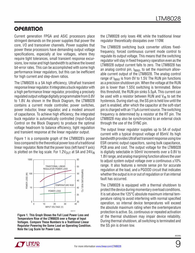
operaTionCurrent generation FPGA and ASIC processors place stringent demands on the power supplies that power the core, I/O and transceiver channels. Power supplies that power these processors have demanding output voltage specifications, especially at low voltages, where they require tight tolerances, small transient response excur-sions, low noise and high bandwidth to achieve the lowest bit-error rates. This can be accomplished with some high performance linear regulators, but this can be inefficient for high current and step-down ratios.
The LTM8028 is a 5A high efficiency, UltraFast transient response linear regulator. It integrates a buck regulator with a high performance linear regulator, providing a precisely regulated output voltage digitally programmable from 0.8V to 1.8V. As shown in the Block Diagram, the LTM8028 contains a current mode controller, power switches, power inductor, linear regulator, and a modest amount of capacitance. To achieve high efficiency, the integrated buck regulator is automatically controlled (Input-Output Control on the Block Diagram) to produce the optimal voltage headroom to balance efficiency, tight regulation and transient response at the linear regulator output.
Figure 1 is a composite graph of the LTM8028’s power loss compared to the theoretical power loss of a traditional linear regulator. Note that the power loss (left hand Y axis) is plotted on the log scale. For 1.2VOUT at 5A and 24VIN
the LTM8028 only loses 4W, while the traditional linear regulator theoretically dissipates over 110W.
The LTM8028 switching buck converter utilizes fixed-frequency, forced continuous current mode control to regulate its output voltage. This means that the switching regulator will stay in fixed frequency operation even as the LTM8028 output current falls to zero. The LTM8028 has an analog control pin, IMAX, to set the maximum allow-able current output of the LTM8028. The analog control range of IMAX is from 0V to 1.5V. The RUN pin functions as a precision shutdown pin. When the voltage at the RUN pin is lower than 1.55V, switching is terminated. Below this threshold, the RUN pin sinks 5.5µA. This current can be used with a resistor between RUN and VIN to set the hysteresis. During start-up, the SS pin is held low until the part is enabled, after which the capacitor at the soft-start pin is charged with an 11μA current source. The switching frequency is determined by a resistor at the RT pin. The LTM8028 may also be synchronized to an external clock through the use of the SYNC pin.
The output linear regulator supplies up to 5A of output current with a typical dropout voltage of 85mV. Its high bandwidth provides UltraFast transient response using low ESR ceramic output capacitors, saving bulk capacitance, PCB area and cost. The output voltage for the LTM8028 is digitally selectable in 50mV increments over a 0.8V to 1.8V range, and analog margining function allows the user to adjust system output voltage over a continuous ±10% range. It also features a remote sense pin for accurate regulation at the load, and a PGOOD circuit that indicates whether the output is in or out of regulation or if an internal fault has occurred.
The LTM8028 is equipped with a thermal shutdown to protect the device during momentary overload conditions. It is set above the 125°C absolute maximum internal tem-perature rating to avoid interfering with normal specified operation, so internal device temperatures will exceed the absolute maximum rating when the overtemperature protection is active. So, continuous or repeated activation of the thermal shutdown may impair device reliability. During thermal shutdown, all switching is terminated and the SS pin is driven low.
INPUT VOLTAGE (V)0
0
POW
ER L
OSS
(W)
TEMPERATURE RISE (°C)
10
100
1000
30
40
50
60
35
45
55
10 20
8028 F01
30 40
TRADITIONAL LINEARREGULATOR POWER LOSS
TEMPERATURE RISE
POWER LOSS
Figure 1. This Graph Shows the Full Load Power Loss and Temperature Rise of the LTM8028 over a Range of Input Voltages. Compare These Numbers to a Traditional Linear Regulator Powering the Same Load an Operating Condition. Note the Log Scale for Power Loss.
LTM8028
108028fb
For more information www.linear.com/LTM8028
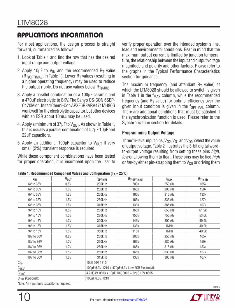
applicaTions inForMaTionFor most applications, the design process is straight forward, summarized as follows:
1. Look at Table 1 and find the row that has the desired input range and output voltage.
2. Apply 10μF to VIN and the recommended RT value (RT(OPTIMAL) in Table 1). Lower RT values (resulting in a higher operating frequency) may be used to reduce the output ripple. Do not use values below RT(MIN).
3. Apply a parallel combination of a 100μF ceramic and a 470μF electrolytic to BKV. The Sanyo OS-CON 6SEP-C470M or United Chemi-Con APXF6R3ARA471MH80G work well for the electrolytic capacitor, but other devices with an ESR about 10mΩ may be used.
4. Apply a minimum of 37μF to VOUT. As shown in Table 1, this is usually a parallel combination of 4.7μF, 10μF and 22μF capacitors.
5. Apply an additional 100µF capacitor to VOUT if very small (2%) transient response is required.
While these component combinations have been tested for proper operation, it is incumbent upon the user to
verify proper operation over the intended system’s line, load and environmental conditions. Bear in mind that the maximum output current is limited by junction tempera-ture, the relationship between the input and output voltage magnitude and polarity and other factors. Please refer to the graphs in the Typical Performance Characteristics section for guidance.
The maximum frequency (and attendant RT value) at which the LTM8028 should be allowed to switch is given in Table 1 in the fMAX column, while the recommended frequency (and RT value) for optimal efficiency over the given input condition is given in the fOPTIMAL column. There are additional conditions that must be satisfied if the synchronization function is used. Please refer to the Synchronization section for details.
Programming Output Voltage
Three tri-level input pins, VO2, VO1 and VO0, select the value of output voltage. Table 2 illustrates the 3-bit digital word-to-output voltage resulting from setting these pins high, low or allowing them to float. These pins may be tied high or low by either pin-strapping them to VOB or driving them
Table 1: Recommended Component Values and Configuration (TA = 25°C)VIN VOUT fOPTIMAL RT(OPTIMAL) fMAX RT(MIN)
6V to 36V 0.8V 200kHz 200k 250kHz 165k6V to 36V 1.0V 250kHz 165k 280kHz 150k6V to 36V 1.2V 250kHz 165k 315kHz 133k6V to 36V 1.5V 250kHz 165k 333kHz 127k6V to 36V 1.8V 315kHz 133k 385kHz 107k9V to 15V 0.8V 250kHz 165k 650kHz 61.9k9V to 15V 1.0V 280kHz 150k 750kHz 53.6k9V to 15V 1.2V 300kHz 143k 800kHz 49.9k9V to 15V 1.5V 315kHz 133k 1MHz 40.2k9V to 15V 1.8V 350kHz 118k 1MHz 40.2k18V to 36V 0.8V 200kHz 200k 250kHz 165k18V to 36V 1.0V 250kHz 165k 280kHz 150k18V to 36V 1.2V 250kHz 165k 315kHz 133k18V to 36V 1.5V 250kHz 165k 333kHz 127k18V to 36V 1.8V 315kHz 133k 385kHz 107k
CIN: 10µF, 50V, 1210CBKV: 100µF, 6.3V, 1210 + 470µF, 6.3V Low ESR Electrolytic COUT: 4.7µF, 4V, 0603 + 10µF, 10V, 0805 + 22µF, 10V, 0805COUT (Optional): 100µF, 6.3V, 1210Note: An input bulk capacitor is required.

LTM8028
118028fb
For more information www.linear.com/LTM8028
applicaTions inForMaTionwith digital ports. Pins that float may either actually float or require logic that has Hi-Z output capability. This allows the output voltage to be dynamically changed if necessary. The output voltage is selectable from a minimum of 0.8V to a maximum of 1.8V in increments of 50mV.
Table 2. VO2 to VO0 Setting vs Output VoltageVO2 VO1 VO0 VOUT(NOM) VO2 VO1 VO0 VOUT(NOM)
0 0 0 0.80V Z 0 1 1.35V
0 0 Z 0.85V Z Z 0 1.40V
0 0 1 0.90V Z Z Z 1.45V
0 Z 0 0.95V Z Z 1 1.50V
0 Z Z 1.00V Z 1 0 1.55V
0 Z 1 1.05V Z 1 Z 1.60V
0 1 0 1.10V Z 1 1 1.65V
0 1 Z 1.15V 1 X 0 1.70V
0 1 1 1.20V 1 X Z 1.75V
Z 0 0 1.25V 1 X 1 1.80V
Z 0 Z 1.30V
X = Don’t Care, 0 = Low, Z = Float, 1 = High
Capacitor Selection Considerations
The CIN, CBKV and COUT capacitor values in Table 1 are the minimum recommended values for the associated oper-ating conditions. Applying capacitor values below those indicated in Table 1 is not recommended, and may result in undesirable operation. Using larger values is generally acceptable, and can yield improved dynamic response, if it is necessary. Again, it is incumbent upon the user to verify proper operation over the intended system’s line, load and environmental conditions.
Ceramic capacitors are small, robust and have very low ESR. However, not all ceramic capacitors are suitable. X5R and X7R types are stable over temperature and ap-plied voltage and give dependable service. Other types, including Y5V and Z5U have very large temperature and voltage coefficients of capacitance. In an application cir-cuit they may have only a small fraction of their nominal capacitance resulting in much higher output voltage ripple than expected.
The output capacitance for BKV given in Table 1 specifies an electrolytic capacitor. Ceramic capacitors may also be used in the application, but it may be necessary to use more of them. Many high value ceramic capacitors have a large voltage coefficient, so the actual capacitance of the component at the desired operating voltage may be only a fraction of the specified value. Also, the very low ESR of ceramic capacitors may necessitate an additional capacitor for acceptable stability margin.
A final precaution regarding ceramic capacitors concerns the maximum input voltage rating of the LTM8028. A ceramic input capacitor combined with trace or cable inductance forms a high Q (under damped) tank circuit. If the LTM8028 circuit is plugged into a live supply, the input voltage can ring to twice its nominal value, possi-bly exceeding the device’s rating. This situation is easily avoided; see the Hot-Plugging Safely section.
Why Do Multiple, Small Value Output Capacitors Connected in Parallel Work Better?
The parasitic series inductance (ESL) and resistance (ESR) of a capacitor can have a detrimental impact on the transient and ripple/noise response of a linear regulator. Employing a number of capacitors in parallel will reduce this parasitic impedance and improve the performance of the linear regulator. In addition, PCB vias can add significant inductance, so the fundamental decoupling capacitors must be mounted on the same copper plane as the LTM8028.
The most area efficient parallel capacitor combination is a graduated 4/2/1 scale capacitances of the same case size, such as the 37μF combination in Table 1, made up of 22μF, 10μF and 4.7μF capacitors in parallel. Capacitors with small case sizes have larger ESR, while those with larger case sizes have larger ESL. As seen in Table 1, the optimum case size is 0805, followed by a larger, fourth bulk energy capacitor, case sized 1210. In general, the large fourth capacitor is required only if very tight transient response is required.

LTM8028
128028fb
For more information www.linear.com/LTM8028
applicaTions inForMaTionOutput Voltage Margining
The LTM8028’s analog margining pin, MARGA, provides a continuous output voltage adjustment range of ±10%. It margins VOUT by adjusting the internal 600mV reference voltage up and down. Driving MARGA with 600mV to 1.2V provides 0% to 10% of adjustment. Driving MARGA with 600mV to 0V provides 0% to –10% of adjustment. If unused, allow MARGA to float or bypass this pin with a 1nF capacitor to GND. Note that the analog margining function does not adjust the PGOOD threshold. Therefore, negative analog margining may trip the PGOOD comparator and toggle the PGOOD flag.
Power Good
PGOOD pin is an open-drain NMOS digital output that ac-tively pulls low if any one of these fault modes is detected:
• VOUT is less than 90% of VOUT(NOMINAL) on the rising edge of VOUT.
• VOUT drops below 85% of VOUT(NOMINAL) for more than 25μs.
• Internal faults such as loss of internal housekeeping voltage regulation, reverse-current on the power switch and excessive temperature.
SENSEP and Load Regulation
The LTM8028 provides a Kelvin sense pin for VOUT, allowing the application to correct for parasitic package and PCB IR drops. If the load is far from the LTM8028, running a separate line from SENSEP to the remote load will correct for IR voltage drops and improve load regulation. SENSEP is the only voltage feedback that the LTM8028 uses to regulate the output, so it must be connected to VOUT, either locally or at the load. In some systems, a loss of feedback signal equates to a loss of output control, potentially
damaging the load. If the SENSEP signal is inadvertently disconnected from the load, internal safety circuits in the LTM8028 prevent the output from running away. This also limits the amount of correction to about 0.2V.
Bear in mind that the linear regulator of the LTM8028 is a high bandwidth power device. If the load is very far from the LTM8028, the parasitic impedance of the remote connection may interfere with the internal control loop and adversely affect stability. If SENSEP is connected to a remote load, the user must evaluate the load regulation and dynamic load response of the LTM8028.
Short-Circuit and Overload Recovery
Like many IC power regulators, the internal linear regulator has safe operating area (SOA) protection. The safe area protection decreases current limit as input-to-output volt-age increases and keeps the power transistor inside a safe operating region for all values of input-to-output voltage up to the absolute maximum voltage rating.
Under maximum ILOAD and maximum VIN-VOUT conditions, the internal linear regulator’s power dissipation peaks at about 1.5W. If ambient temperature is high enough, die junction temperature will exceed the 125°C maximum operating temperature. If this occurs, the LTM8028 relies on two additional thermal safety features. At about 145°C, the device is designed to make the PGOOD output pull low providing an early warning of an impending thermal shutdown condition. At 165°C typically, the LTM8028 is designed to engage its thermal shutdown and the output is turned off until the IC temperature falls below the thermal hysteresis limit. The SOA protection decreases current limit as the in-to-out voltage increases and keeps the power dissipation at safe levels for all values of input-to-output voltage.
LTM8028
138028fb
For more information www.linear.com/LTM8028
applicaTions inForMaTionReverse Voltage
The LTM8028 incorporates a circuit that detects if BKV decreases below VOUT. If this voltage condition is detected, internal circuitry turns off the drive to the internal linear regulator’s pass transistor, thereby turning off the output. This circuit’s intent is to limit and prevent back-feed current from VOUT to VIN if the input voltage collapses due to a fault or overload condition. Do not apply a voltage to BKV.
Programming Switching Frequency
The LTM8028 has an operational switching frequency range between 200kHz and 1MHz. This frequency is programmed with an external resistor from the RT pin to ground. Do not leave this pin open under any condition. The RT pin is also current limited to 60μA. See Table 3 for resistor values and the corresponding switching frequencies.
Table 3. RT Resistor Values and Their Resultant Switching Frequencies
SWITCHING FREQUENCY (MHz) RT (kΩ)1 40.2
0.750 53.60.5 82.50.3 1430.2 200
Switching Frequency Trade-Offs
It is recommended that the user apply the optimal RT value given in Table 1 for the input and output operating condi-tion. System level or other considerations, however, may necessitate another operating frequency. A higher switching frequency, for example, will yield a smaller output ripple, while a lower frequency will reduce power loss. Switch-ing too fast, however, can generate excessive heat and even possibly damage the LTM8028 in fault conditions. Switching too slow can result in a final design that has too much output capacitance or sub-harmonic oscillations that cause excessive ripple. In all cases, stay below the stated maximum frequency (fMAX) given in Table 1.
Switching Frequency Synchronization
The nominal switching frequency of the LTM8028 is determined by the resistor from the RT pin to GND and may be set from 200kHz to 1MHz. The internal oscillator may also be synchronized to an external clock through the SYNC pin. The external clock applied to the SYNC pin must have a logic low below 0.25V and a logic high greater than 1.25V. The input frequency must be 20% higher than the frequency determined by the resistor at the RT pin. The duty cycle of the input signal needs to be greater than 10% and less than 90%. Input signals outside of these specified parameters will cause erratic switching behavior and subharmonic oscillations. When synchronizing to an external clock, please be aware that there will be a fixed delay from the input clock edge to the edge of switch. The SYNC pin must be tied to GND if the synchronization to an external clock is not required. When SYNC is grounded, the switching frequency is determined by the resistor at the RT pin.
Soft-Start
The soft-start function controls the slew rate of the power supply output voltage during start-up. A controlled output voltage ramp minimizes output voltage overshoot, reduces inrush current from the VIN supply, and facilitates supply sequencing. A capacitor connected from the SS pin to GND programs the slew rate. The capacitor is charged from an internal 11μA current source to produce a ramped output voltage.
Maximum Output Current Adjust
To adjust the regulated load current, an analog voltage is applied to the IMAX pin. Varying the voltage between 0V and 1.5V adjusts the maximum current between the minimum and the maximum current, 5.6A typical. Above 1.5V, the control voltage has little effect on the regulated inductor current. A graph of the output current versus IMAX voltage is given in the Typical Performance Characteristics
LTM8028
148028fb
For more information www.linear.com/LTM8028
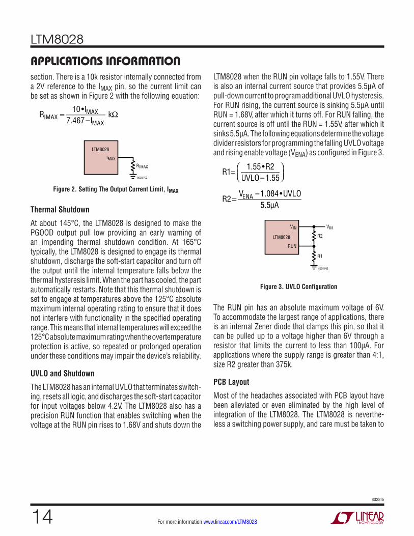
section. There is a 10k resistor internally connected from a 2V reference to the IMAX pin, so the current limit can be set as shown in Figure 2 with the following equation:
RIMAX = 10 •IMAX
7.467 –IMAX kΩ
applicaTions inForMaTionLTM8028 when the RUN pin voltage falls to 1.55V. There is also an internal current source that provides 5.5μA of pull-down current to program additional UVLO hysteresis. For RUN rising, the current source is sinking 5.5µA until RUN = 1.68V, after which it turns off. For RUN falling, the current source is off until the RUN = 1.55V, after which it sinks 5.5µA. The following equations determine the voltage divider resistors for programming the falling UVLO voltage and rising enable voltage (VENA) as configured in Figure 3.
R1= 1.55 •R2UVLO–1.55
R2=VENA –1.084 •UVLO
5.5µA
Figure 2. Setting The Output Current Limit, IMAX
IMAX
RIMAX
8028 F02
LTM8028
Thermal Shutdown
At about 145°C, the LTM8028 is designed to make the PGOOD output pull low providing an early warning of an impending thermal shutdown condition. At 165°C typically, the LTM8028 is designed to engage its thermal shutdown, discharge the soft-start capacitor and turn off the output until the internal temperature falls below the thermal hysteresis limit. When the part has cooled, the part automatically restarts. Note that this thermal shutdown is set to engage at temperatures above the 125°C absolute maximum internal operating rating to ensure that it does not interfere with functionality in the specified operating range. This means that internal temperatures will exceed the 125°C absolute maximum rating when the overtemperature protection is active, so repeated or prolonged operation under these conditions may impair the device’s reliability.
UVLO and Shutdown
The LTM8028 has an internal UVLO that terminates switch-ing, resets all logic, and discharges the soft-start capacitor for input voltages below 4.2V. The LTM8028 also has a precision RUN function that enables switching when the voltage at the RUN pin rises to 1.68V and shuts down the
VIN VIN
RUN
R2
R1
8028 F03
LTM8028
Figure 3. UVLO Configuration
The RUN pin has an absolute maximum voltage of 6V. To accommodate the largest range of applications, there is an internal Zener diode that clamps this pin, so that it can be pulled up to a voltage higher than 6V through a resistor that limits the current to less than 100µA. For applications where the supply range is greater than 4:1, size R2 greater than 375k.
PCB Layout
Most of the headaches associated with PCB layout have been alleviated or even eliminated by the high level of integration of the LTM8028. The LTM8028 is neverthe-less a switching power supply, and care must be taken to

LTM8028
158028fb
For more information www.linear.com/LTM8028
minimize EMI and ensure proper operation. Even with the high level of integration, you may fail to achieve specified operation with a haphazard or poor layout. See Figure 4 for a suggested layout. Ensure that the grounding and heat sinking are acceptable.
A few rules to keep in mind are:
1. Place the RT resistor as close as possible to its respec-tive pins.
2. Place the CIN capacitor as close as possible to the VIN and GND connection of the LTM8028.
3. Place the COUT capacitors as close as possible to the VOUT and GND connection of the LTM8028.
4. Place the CIN, CBKV and COUT capacitors such that their ground current flow directly adjacent or underneath the LTM8028.
5. Connect all of the GND connections to as large a copper pour or plane area as possible on the top layer. Avoid breaking the ground connection between the external components and the LTM8028.
6. Use vias to connect the GND copper area to the board’s internal ground planes. Liberally distribute these GND vias to provide both a good ground connection and thermal path to the internal planes of the printed circuit board. Pay attention to the location and density of the thermal vias in Figure 4. The LTM8028 can benefit from the heat sinking afforded by vias that connect to internal GND planes at these locations, due to their proximity to internal power handling components. The optimum number of thermal vias depends upon the printed circuit board design. For example, a board might use very small via holes. It should employ more thermal vias than a board that uses larger holes.
applicaTions inForMaTion
Figure 4. Layout Showing Suggested External Components, GND Plane and Thermal Vias
SENSEP
(OUTPUT ISSET TO 1.55V)
GND
BKV CBKVCOUT
VOUT
RUN
CIN
8028 F04
VINGND
THERMAL VIAS
GND
RT
SS SYNC
IMAX
TEST
MARGAPGOOD
VO0VO1
VO2VOB

LTM8028
168028fb
For more information www.linear.com/LTM8028
Load Sharing
Each LTM8028 features an accurate current limit that en-ables the use of multiple devices to power a load heavier than 5A. This is accomplished by simply tying the VOUT terminals of the LTM8028s together, and set the outputs of the parallel units to the same voltage. There is no need to power the μModule regulators from the same power supply. That is, the application can use multiple LTM8028s, each powered from separate input voltage rails and contribute a different amount of current to the load as dictated by the programmed current limit. Keep in mind that the paralleled LTM8028s will not share current equally. In most cases, one LTM8028 will provide almost all the load until its current limit is reached, and then the other unit or units will start to provide current. This might be an unacceptable operat-ing condition in other power regulators, but the accurate current loop of the LTM8028 controls the electrical and thermal performance of each individual μModule regulator. This prevents the oscillations, thermal runaway and other issues that other regulators might suffer. An example of two LTM8028s connected in parallel to deliver 1.8V at 10A, while powered from two disparate power sources, is given in the Typical Applications section. A graph of the output current delivered from each μModule regulator is given below in Figure 5.
Hot-Plugging Safely
The small size, robustness and low impedance of ceramic capacitors make them an attractive option for the input bypass capacitor of LTM8028. However, these capacitors can cause problems if the LTM8028 is plugged into a live input supply (see Application Note 88 for a complete dis-cussion). The low loss ceramic capacitor combined with stray inductance in series with the power source forms an underdamped tank circuit, and the voltage at the VIN pin of the LTM8028 can ring to more than twice the nominal input voltage, possibly exceeding the LTM8028’s rating and damaging the part. If the input supply is poorly con-trolled or the user will be plugging the LTM8028 into an energized supply, the input network should be designed to prevent this overshoot. This can be accomplished by installing a small resistor in series to VIN, but the most popular method of controlling input voltage overshoot is to add an electrolytic bulk capacitor to the VIN net. This capacitor’s relatively high equivalent series resistance damps the circuit and eliminates the voltage overshoot. The extra capacitor improves low frequency ripple filter-ing and can slightly improve the efficiency of the circuit, though it is physically large.
applicaTions inForMaTion
TOTAL LOAD CURRENT (A)1
0
CURR
ENT
DELI
VERE
D BY
LTM
8028
s (A
)
1
2
3
4
5
6
2 4 6 8
8028 F05
10
Figure 5. In Most Cases Where Paralleled LTM8028s are Used, One µModule Will Deliver All of The Load Current Until Its Current Limit Is Reached, Then The Other Unit(s) Will Provide Current. The Tightly Controlled Output Current Prevents Oscillations and Thermal Runaway Observed In Other Types of Regulators
LTM8028
178028fb
For more information www.linear.com/LTM8028
applicaTions inForMaTionThermal Considerations
The LTM8028 relies on two thermal safety features. At about 145°C, the device is designed to pull the PGOOD output low providing an early warning of an impending thermal shutdown condition. At 165°C typically, the LTM8028 is designed to engage its thermal shutdown and the output is turned off until the IC temperature falls below the thermal hysteresis limit. Note that these temperature thresholds are above the 125°C absolute maximum rating to avoid interfering with normal operation. Thus, prolonged or repetitive operation under a condition in which the thermal shutdown activates may damage or impair the reliability of the device.
The LTM8028 output current may need to be derated if it is required to operate in a high ambient temperature. The amount of current derating is dependent upon the input voltage, output power and ambient temperature. The temperature rise curves given in the Typical Performance Characteristics section can be used as a guide. These curves were generated by the LTM8028 mounted to a 58cm2 4-layer FR4 printed circuit board. Boards of other sizes and layer count can exhibit different thermal behavior, so it is incumbent upon the user to verify proper operation over the intended system’s line, load and environmental operating conditions.
For increased accuracy and fidelity to the actual application, many designers use finite element analysis (FEA) to predict thermal performance. To that end, the Pin Configuration of the data sheet typically gives four thermal coefficients:
θJA – Thermal resistance from junction to ambient
θJCbottom – Thermal resistance from junction to the bottom of the product case
θJCtop – Thermal resistance from junction to top of the product case
θJBoard – Thermal resistance from junction to the printed circuit board.
While the meaning of each of these coefficients may seem to be intuitive, JEDEC has defined each to avoid confusion and inconsistency. These definitions are given in JESD 51-12, and are quoted or paraphrased below:
θJA is the natural convection junction-to-ambient air thermal resistance measured in a one cubic foot sealed enclosure. This environment is sometimes referred to as “still air” although natural convection causes the air to move. This value is determined with the part mounted to a JESD 51-9 defined test board, which does not reflect an actual application or viable operating condition.
θJCbottom is the junction-to-board thermal resistance with all of the component power dissipation flowing through the bottom of the package. In the typical µModule regulator, the bulk of the heat flows out the bottom of the package, but there is always heat flow out into the ambient envi-ronment. As a result, this thermal resistance value may be useful for comparing packages but the test conditions don’t generally match the user’s application.
θJCtop is determined with nearly all of the component power dissipation flowing through the top of the package. As the electrical connections of the typical µModule regulator are on the bottom of the package, it is rare for an application to operate such that most of the heat flows from the junc-tion to the top of the part. As in the case of θJCbottom, this value may be useful for comparing packages but the test conditions don’t generally match the user’s application.
θJB is the junction-to-board thermal resistance where almost all of the heat flows through the bottom of the µModule regulator and into the board, and is really the sum of the θJCbottom and the thermal resistance of the bottom of the part through the solder joints and through a portion of the board. The board temperature is measured a specified distance from the package, using a 2-sided, 2-layer board. This board is described in JESD 51-9.

LTM8028
188028fb
For more information www.linear.com/LTM8028
1V at 5A Regulator with 2% Transient ResponseTransient Response from 0.5A to 5A, 1µs Load Current Rise and Fall Time, 12VIN
LOADCURRENT
2A/DIV
VOUT20mV/DIV
1µs/DIV 8028 TA03
Typical applicaTions
Given these definitions, it should now be apparent that none of these thermal coefficients reflects an actual physical operating condition of a µModule regulator. Thus, none of them can be individually used to accurately predict the thermal performance of the product. Likewise, it would be inappropriate to attempt to use any one coefficient to correlate to the junction temperature vs load graphs given in the product’s data sheet. The only appropriate way to use the coefficients is when running a detailed thermal analysis, such as FEA, which considers all of the thermal resistances simultaneously.
A graphical representation of these thermal resistances is given in Figure 6:
The blue resistances are contained within the µModule regulator, and the green are outside.
The die temperature of the LTM8028 must be lower than the maximum rating of 125°C, so care should be taken in the layout of the circuit to ensure good heat sinking of the LTM8028. The bulk of the heat flow out of the LTM8028 is through the bottom of the module and the LGA pads into the printed circuit board. Consequently a poor printed circuit board design can cause excessive heating, result-ing in impaired performance or reliability. Please refer to the PCB Layout section for printed circuit board design suggestions.
applicaTions inForMaTion
8028 F06
µMODULE DEVICE
JUNCTION-TO-CASE (TOP)RESISTANCE
JUNCTION-TO-BOARD RESISTANCE
JUNCTION-TO-AMBIENT RESISTANCE (JESD 51-9 DEFINED BOARD)
CASE (TOP)-TO-AMBIENTRESISTANCE
BOARD-TO-AMBIENTRESISTANCE
JUNCTION-TO-CASE(BOTTOM) RESISTANCE
JUNCTION AMBIENT
CASE (BOTTOM)-TO-BOARDRESISTANCE
Figure 6. Thermal Model of µModule
+
LINEARREGULATOR
VIN VOUT
SENSEP
BKV
RUN402k
VIN6V TO 36V
165k
0.01µFMARGAIMAX
SS PGOOD
100µFRT GND VOB VO0 VO1 VO2
470µF
*137µF = 4.7µF + 10µF + 22µF +100µF IN PARALLEL
8028 TA02
137µF*
VOUT1V5A
SYNC
LTM8028
10µF
LTM8028
198028fb
For more information www.linear.com/LTM8028
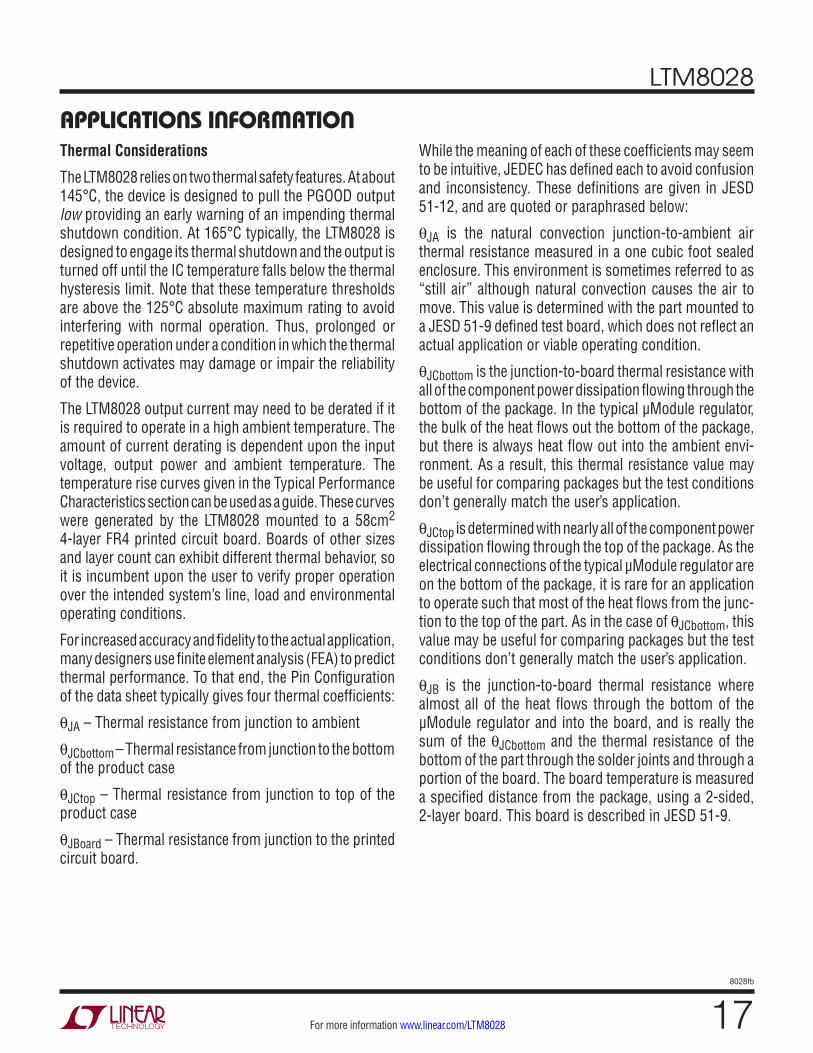
1.8V Regulator with 3.5A Current Limit
OUTPUT CURRENT (A)0
0
OUTP
UT V
OLTA
GE (V
)
0.2
0.6
0.8
1.0
2.0
1.4
1 2
8028 TA05
0.4
1.6
1.8
1.2
3 4
Output Voltage vs Current
+
LINEARREGULATOR
VIN VOUT
SENSEP
BKV
RUN402k
10k
VIN6V TO 36V
133k0.01µF
MARGA
IMAX
SS PGOOD
100µFRT GND VOB VO0 VO1 VO2
470µF
*37µF = 4.7µF + 10µF + 22µF IN PARALLEL
8028 TA04
37µF*
VOUT1.8V3.5A
SYNC
LTM8028
10µF
Typical applicaTions
1.8V, 10A with Two LTM8028s Powered from Two Different Sources Each µModule Regulator Is Limited to Provide a Maximum of 5A
+
LINEARREGULATOR
VIN VOUT
SENSEP
BKV
RUN402k
20.5k
VIN24V
133k0.01µF
MARGA
IMAX
SS PGOOD
100µFRT GND VOB VO0 VO1 VO2
330µF
*17µF = 2.2µF + 4.7µF + 10µF IN PARALLEL
17µF*
VOUT1.8V10A
SYNC
LTM8028
10µF
+
LINEARREGULATOR
VIN VOUT
SENSEP
BKV
RUN150k
20.5k
VIN12V
133k0.01µF
MARGA
IMAX
SS PGOOD
100µFRT GND VOB VO0 VO1 VO2
330µF8028 TA06
17µF*
SYNC
LTM8028
10µF

LTM8028
208028fb
For more information www.linear.com/LTM8028
Low Noise LTM8028 Powering 16-Bit, 125Msps ADC
32k-Point FFT, fIN = 70.3MHz, –1dBFS, 100Msps
Typical applicaTions
+
LINEARREGULATOR
VIN VOUT
SENSEP
BKV
RUN402k
VIN6V TO 36V
133k
0.01µFMARGAIMAX
SS PGOOD
100µFRT GND VOB VO0 VO1 VO2
470µF
AIN+
VDD
ENC+ ENC–
LTC®2185 ADC
GND
OVDD
AIN–
8028 TA08a
137µF*
1.8V0V
VOUT1.8V5A
SYNC
LTM8028
10µF
*137µF = 4.7µF + 10µF + 22µF + 100µF IN PARALLEL
FREQUENCY (MHz)0
MAG
NITU
DE (d
BFS)
–60
–40
–20
0
40
8028 TA08b
–80
–100
–70
–50
–30
–10
–90
–110
–12010 20 30 50

LTM8028
218028fb
For more information www.linear.com/LTM8028
package DescripTion
package phoTo
Table 3. Pin Assignment Table (Arranged by Pin Number)
PIN NAME PIN NAME PIN NAME PIN NAME PIN NAME PIN NAMEA1 GND B1 GND C1 GND D1 IMAX E1 RT F1 RUNA2 GND B2 GND C2 GND D2 SS E2 SYNC F2 GNDA3 GND B3 GND C3 GND D3 GND E3 GND F3 GNDA4 GND B4 GND C4 GND D4 GND E4 GND F4 GNDA5 VO2 B5 VOB C5 GND D5 GND E5 GND F5 GNDA6 VO0 B6 VO1 C6 GND D6 GND E6 GND F6 GNDA7 MARGA B7 PGOOD C7 GND D7 GND E7 GND F7 GNDA8 TEST B8 GND C8 GND D8 GND E8 GND F8 GNDA9 SENSEP B9 GND C9 GND D9 GND E9 GND F9 GNDA10 VOUT B10 VOUT C10 VOUT D10 VOUT E10 VOUT F10 VOUT
A11 VOUT B11 VOUT C11 VOUT D11 VOUT E11 VOUT D11 VOUT
PIN NAME PIN NAME PIN NAME PIN NAM PIN NAMEG1 – H1 VIN J1 VIN K1 VIN L1 VIN
G2 – H2 VIN J2 VIN K2 VIN L2 VIN
G3 – H3 – J3 – K3 – L3 –G4 GND H4 GND J4 GND K4 GND L4 GNDG5 GND H5 GND J5 GND K5 GND L5 GNDG6 GND H6 GND J6 GND K6 GND L6 GNDG7 GND H7 GND J7 GND K7 GND L7 GNDG8 GND H8 GND J8 GND K8 GND L8 GNDG9 GND H9 GND J9 BKV K9 BKV L9 BKVG10 GND H10 GND J10 BKV K10 BKV L10 BKVG11 GND H11 GND J11 BKV K11 BKV L11 BKV
LTM8028
228028fb
For more information www.linear.com/LTM8028
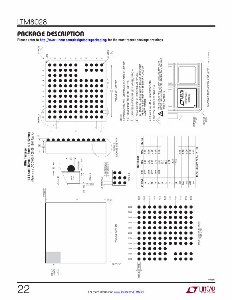
package DescripTionPlease refer to http://www.linear.com/designtools/packaging/ for the most recent package drawings.
6.350
6.350
3.810
3.810
5.080
5.080
2.540
2.540
1.270
1.270
BGA
Pack
age
114-
Lead
(15m
m ×
15m
m ×
4.9
2mm
)(R
efer
ence
LTC
DW
G #
05-0
8-18
94 R
ev A
)
NOTE
S:1.
DIM
ENSI
ONIN
G AN
D TO
LERA
NCIN
G PE
R AS
ME
Y14.
5M-1
994
2. A
LL D
IMEN
SION
S AR
E IN
MIL
LIM
ETER
S
LAN
D DE
SIGN
ATIO
N PE
R JE
SD M
O-22
2, S
PP-0
10
5. P
RIM
ARY
DATU
M -Z
- IS
SEAT
ING
PLAN
E
6. T
HE T
OTAL
NUM
BER
OF P
ADS:
114
43
DETA
ILS
OF P
AD #
1 ID
ENTI
FIER
ARE
OPT
IONA
L,BU
T M
UST
BE L
OCAT
ED W
ITHI
N TH
E ZO
NE IN
DICA
TED.
THE
PAD
#1 ID
ENTI
FIER
MAY
BE
EITH
ER A
MOL
D OR
M
ARKE
D FE
ATUR
E
PACK
AGE
TOP
VIEW
4
PAD
“A1”
CORN
ER
X
Y
aaa
Z
aaa Z
PACK
AGE
BOTT
OM V
IEW
3
SEE
NOTE
S
SUGG
ESTE
D PC
B LA
YOUT
TOP
VIEW
DETA
IL A
PAD
1
0.000
6.35
0
6.35
0
3.81
0
3.81
0
5.08
0
5.08
0
2.54
0
2.54
0
1.27
0
1.27
0
0.00
0
F G H LJ KEA B C D
21
43
119
510
67
8
D
0.63
0 ±0
.025
Ø 1
14x
E
b
e
e
b
F
G
BGA
114
1112
REV
A
TRAY
PIN
1BE
VEL
PACK
AGE
IN T
RAY
LOAD
ING
ORIE
NTAT
ION
COM
PONE
NTPI
N “A
1”
LTM
XXXX
XXµM
odul
e
DETA
IL A
Øb (1
14 P
LACE
S)
DETA
IL B
SUBS
TRAT
E
0.27
– 0
.37
3.95
– 4
.05
// bbb Z
A
A1
b1
ccc
Z
DETA
IL B
PACK
AGE
SIDE
VIE
W
MOL
DCA
P
Z
MX
YZ
ddd
MZ
eee
A2
SYM
BOL
A A1 A2 b b1 D E e F G aaa
bbb
ccc
ddd
eee
MIN
4.72
0.50
4.22
0.60
0.60
NOM
4.92
0.60
4.32
0.75
0.63
15.0
15.0
1.27
12.7
012
.70
MAX
5.12
0.70
4.42
0.90
0.66
0.15
0.10
0.20
0.30
0.15
NOTE
S
DIM
ENSI
ONS
TOTA
L NU
MBE
R OF
BAL
LS: 1
14
7PA
CKAG
E RO
W A
ND C
OLUM
N LA
BELI
NG M
AY V
ARY
AMON
G µM
odul
e PR
ODUC
TS. R
EVIE
W E
ACH
PACK
AGE
LAYO
UT C
AREF
ULLY
!
7
SEE
NOTE
S

LTM8028
238028fb
For more information www.linear.com/LTM8028
Information furnished by Linear Technology Corporation is believed to be accurate and reliable. However, no responsibility is assumed for its use. Linear Technology Corporation makes no representa-tion that the interconnection of its circuits as described herein will not infringe on existing patent rights.
revision hisToryREV DATE DESCRIPTION PAGE NUMBER
A 2/14 Added SnPb BGA package option 1, 2
B 5/14 SYNC Input Threshold MIN: from 0.8V to 0.6V; MAX: from 1.2V to 1.3VAdd PGOOD description
37
LTM8028
248028fb
For more information www.linear.com/LTM8028 LINEAR TECHNOLOGY CORPORATION 2013
LT 0614 REV B • PRINTED IN USALinear Technology Corporation1630 McCarthy Blvd., Milpitas, CA 95035-7417(408) 432-1900 FAX: (408) 434-0507 www.linear.com/LTM8028
relaTeD parTs
Typical applicaTion
PART NUMBER DESCRIPTION COMMENTS
LTM8032 Step-Down µModule Regulator, EN55022B Compliant 3.6V ≤ VIN ≤ 36V, 0.8V ≤ VOUT ≤ 10V, 2A
LTM4613 Step-Down µModule Regulator, EN55022B Compliant 5V ≤ VIN ≤ 36V, 3.3V ≤ VOUT ≤ 15V, 8A
LTM8027 60V, 4A Step-Down µModule Regulator 4.5V ≤ VIN ≤ 60V, 2.5V ≤ VOUT ≤ 24V, 4A
LTM8048 Isolated µModule Converter 725V Isolation, 3.1V ≤ VIN ≤ 32V, 1.2V ≤ VOUT ≤ 12V, 300mA
LTM4615 Triple Output Step-Down µModule Regulator 2.375V ≤ VIN ≤ 5.5V, 0.8V ≤ VOUT ≤ 5.5V, 4A, 4A, 1.5A
LTM4620 Dual 13A, Single 26A Step-Down µModule Regulator 4.5V ≤ VIN ≤ 16V, 0.6V ≤ VOUT ≤ 2.5V, Up to 100A Current Sharing
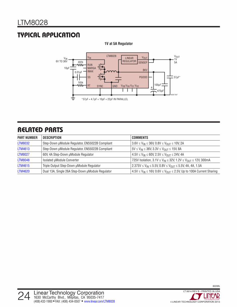
1V at 5A Regulator
+
LINEARREGULATOR
VIN VOUT
SENSEP
BKV
RUN402k
VIN6V TO 36V
165k
0.01µFMARGAIMAX
SS PGOOD
100µFRT GND VOB VO0 VO1 VO2
470µF
*37µF = 4.7µF + 10µF + 22µF IN PARALLEL
8028 TA07
37µF*
VOUT1V5A
SYNC
LTM8028
10µF


