High Output Current, Rail-to-Rail Input/Output Dual CMOS ...
LTC6090/LTC6090-5
16090fe
For more information www.linear.com/LTC6090
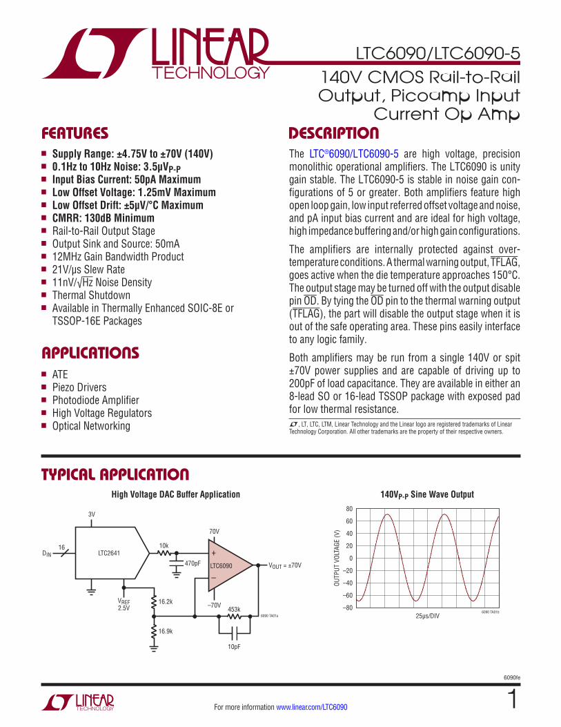
TYPICAL APPLICATION
FEATURES DESCRIPTION
140V CMOS Rail-to-Rail Output, Picoamp Input
Current Op Amp
The LTC®6090/LTC6090-5 are high voltage, precision monolithic operational amplifiers. The LTC6090 is unity gain stable. The LTC6090-5 is stable in noise gain con-figurations of 5 or greater. Both amplifiers feature high open loop gain, low input referred offset voltage and noise, and pA input bias current and are ideal for high voltage, high impedance buffering and/or high gain configurations.
The amplifiers are internally protected against over-temperature conditions. A thermal warning output, TFLAG, goes active when the die temperature approaches 150°C. The output stage may be turned off with the output disable pin OD. By tying the OD pin to the thermal warning output (TFLAG), the part will disable the output stage when it is out of the safe operating area. These pins easily interface to any logic family.
Both amplifiers may be run from a single 140V or spit ±70V power supplies and are capable of driving up to 200pF of load capacitance. They are available in either an 8-lead SO or 16-lead TSSOP package with exposed pad for low thermal resistance.
140VP-P Sine Wave Output
APPLICATIONS
n Supply Range: ±4.75V to ±70V (140V)n 0.1Hz to 10Hz Noise: 3.5μVP-P n Input Bias Current: 50pA Maximumn Low Offset Voltage: 1.25mV Maximumn Low Offset Drift: ±5µV/°C Maximumn CMRR: 130dB Minimumn Rail-to-Rail Output Stagen Output Sink and Source: 50mAn 12MHz Gain Bandwidth Productn 21V/µs Slew Raten 11nV/√Hz Noise Densityn Thermal Shutdownn Available in Thermally Enhanced SOIC-8E or
TSSOP-16E Packages
n ATEn Piezo Driversn Photodiode Amplifiern High Voltage Regulatorsn Optical Networking
High Voltage DAC Buffer Application
VOUT = ±70V
6090 TA01a
–
+LTC6090
453k
10pF
70V
3V
–70V16.2k
10k
470pF
16.9k
VREF2.5V
LTC2641DIN16
25µs/DIV
80
60
40
20
0
–20
–40
–60
–806090 TA01b
OUTP
UT V
OLTA
GE (V
)
L, LT, LTC, LTM, Linear Technology and the Linear logo are registered trademarks of Linear Technology Corporation. All other trademarks are the property of their respective owners.
LTC6090/LTC6090-5
26090fe
For more information www.linear.com/LTC6090
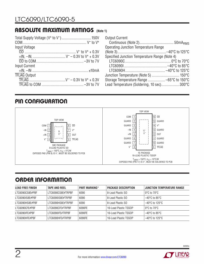
PIN CONFIGURATION
ABSOLUTE MAXIMUM RATINGSTotal Supply Voltage (V+ to V–) ...............................150VCOM ................................................................... V– to V+
Input Voltage OD ...................................................... V– to V+ + 0.3V +IN, –IN, ..................................V– – 0.3V to V+ + 0.3V OD to COM .................................................. –3V to 7V
Input Current +IN, –IN ........................................................... ±10mA
TFLAG Output TFLAG ......................................V– – 0.3V to V+ + 0.3V TFLAG to COM ............................................ –3V to 7V
(Note 1)
1
2
3
4
8
7
6
5
TOP VIEW
9 V–
OD
V+
OUT
TFLAG
COM
–IN
+IN
V–
S8E PACKAGE8-LEAD PLASTIC SO
TJMAX = 150°C, θJC = 5°C/W EXPOSED PAD (PIN 9) IS V–, MUST BE SOLDERED TO PCB FE PACKAGE
16-LEAD PLASTIC TSSOP
1
2
3
4
5
6
7
8
TOP VIEW
16
15
14
13
12
11
10
9
COM
GUARD
GUARD
–IN
+IN
GUARD
GUARD
V–
17 V–
OD
GUARD
V+
GUARD
OUT
GUARD
GUARD
TFLAG
TJMAX = 150°C, θJC = 10°C/W
EXPOSED PAD (PIN 17) IS V–, MUST BE SOLDERED TO PCB
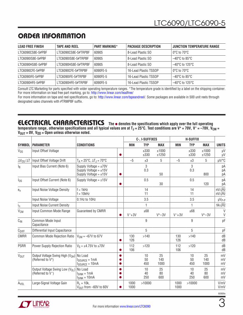
ORDER INFORMATIONLEAD FREE FINISH TAPE AND REEL PART MARKING* PACKAGE DESCRIPTION JUNCTION TEMPERATURE RANGE
LTC6090CS8E#PBF LTC6090CS8E#TRPBF 6090 8-Lead Plastic SO 0°C to 70°C
LTC6090IS8E#PBF LTC6090IS8E#TRPBF 6090 8-Lead Plastic SO –40°C to 85°C
LTC6090HS8E#PBF LTC6090HS8E#TRPBF 6090 8-Lead Plastic SO –40°C to 125°C
LTC6090CFE#PBF LTC6090CFE#TRPBF 6090FE 16-Lead Plastic TSSOP 0°C to 70°C
LTC6090IFE#PBF LTC6090IFE#TRPBF 6090FE 16-Lead Plastic TSSOP –40°C to 85°C
LTC6090HFE#PBF LTC6090HFE#TRPBF 6090FE 16-Lead Plastic TSSOP –40°C to 125°C
Output Current Continuous (Note 2).................................... 50mARMS
Operating Junction Temperature Range (Note 3) ...................................................–40°C to 125°CSpecified Junction Temperature Range (Note 4)
LTC6090C ................................................ 0°C to 70°C LTC6090I .............................................–40°C to 85°C LTC6090H .......................................... –40°C to 125°C
Junction Temperature (Note 5) ............................. 150°CStorage Temperature Range .................. –65°C to 150°CLead Temperature (Soldering, 10 sec) ................... 300°C
LTC6090/LTC6090-5
36090fe
For more information www.linear.com/LTC6090
ELECTRICAL CHARACTERISTICS The l denotes the specifications which apply over the full operating temperature range, otherwise specifications and all typical values are at TJ = 25°C. Test conditions are V+ = 70V, V– = –70V, VCM = VOUT = 0V, VOD = Open unless otherwise noted.
ORDER INFORMATION
C-, I-SUFFIXES H-SUFFIX
SYMBOL PARAMETER CONDITIONS MIN TYP MAX MIN TYP MAX UNITS
VOS Input Offset Voltage
l
±330 ±330
±1000 ±1250
±330 ±330
±1000 ±1250
μV μV
∆VOS /∆T Input Offset Voltage Drift TA = 25°C, ∆TJ = 70°C –5 ±3 5 –5 ±3 5 µV/°C
IB Input Bias Current (Note 6) Supply Voltage = ±70V Supply Voltage = ±15V Supply Voltage = ±15V
l
3 0.3
50
3 0.3
800
pA pA pA
IOS Input Offset Current (Note 6) Supply Voltage = ±15V
l
0.5 30
0.5 120
pA pA
en Input Noise Voltage Density f = 1kHz f = 10kHz
14 11
14 11
nV/√Hz nV/√Hz
Input Noise Voltage 0.1Hz to 10Hz 3.5 3.5 µVP-P
in Input Noise Current Density 1 1 fA/√Hz
VCM Input Common Mode Range Guaranteed by CMRR
l
V–+3V
±68 V+–3V
V–+3V
±68 V+–3V
V V
CIN Common Mode Input Capacitance
9 9 pF
CDIFF Differential Input Capacitance 5 5 pF
CMRR Common Mode Rejection Ratio VCM = –67V to 67V
l
130 126
>140 130 126
>140 dB dB
PSRR Power Supply Rejection Ratio VS = ±4.75V to ±70V
l
112 106
>120 112 106
>120 dB dB
VOUT Output Voltage Swing High (VOH) (Referred to V+)
No Load ISOURCE = 1mA ISOURCE = 10mA
l
l
l
10 50
450
25 140
1000
10 50
450
25 140
1000
mV mV mV
Output Voltage Swing Low (VOL) (Referred to V–)
No Load ISINK = 1mA ISINK = 10mA
l
l
l
10 40
250
25 80
600
10 40
250
25 80
600
mV mV mV
AVOL Large-Signal Voltage Gain RL = 10k, VOUT from –60V to 60V
l
1000 1000
>10000 1000 1000
>10000 V/mV V/mV
LEAD FREE FINISH TAPE AND REEL PART MARKING* PACKAGE DESCRIPTION JUNCTION TEMPERATURE RANGE
LTC6090CS8E-5#PBF LTC6090CS8E-5#TRPBF 60905 8-Lead Plastic SO 0°C to 70°C
LTC6090IS8E-5#PBF LTC6090IS8E-5#TRPBF 60905 8-Lead Plastic SO –40°C to 85°C
LTC6090HS8E-5#PBF LTC6090HS8E-5#TRPBF 60905 8-Lead Plastic SO –40°C to 125°C
LTC6090CFE-5#PBF LTC6090CFE-5#TRPBF 6090FE-5 16-Lead Plastic TSSOP 0°C to 70°C
LTC6090IFE-5#PBF LTC6090IFE-5#TRPBF 6090FE-5 16-Lead Plastic TSSOP –40°C to 85°C
LTC6090HFE-5#PBF LTC6090HFE-5#TRPBF 6090FE-5 16-Lead Plastic TSSOP –40°C to 125°C
Consult LTC Marketing for parts specified with wider operating temperature ranges. *The temperature grade is identified by a label on the shipping container. For more information on lead free part marking, go to: http://www.linear.com/leadfree/ For more information on tape and reel specifications, go to: http://www.linear.com/tapeandreel/. Some packages are available in 500 unit reels through designated sales channels with #TRMPBF suffix.
LTC6090/LTC6090-5
46090fe
For more information www.linear.com/LTC6090
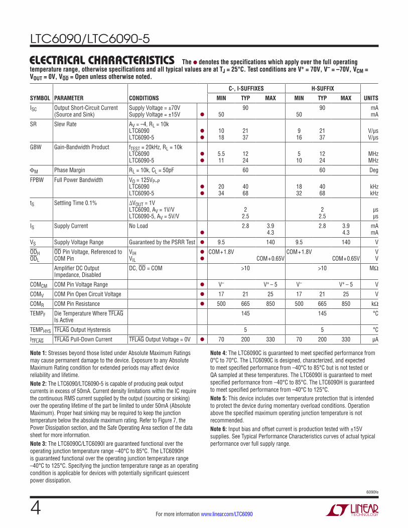
ELECTRICAL CHARACTERISTICS The l denotes the specifications which apply over the full operating temperature range, otherwise specifications and all typical values are at TJ = 25°C. Test conditions are V+ = 70V, V– = –70V, VCM = VOUT = 0V, VOD = Open unless otherwise noted.
C-, I-SUFFIXES H-SUFFIX
SYMBOL PARAMETER CONDITIONS MIN TYP MAX MIN TYP MAX UNITS
ISC Output Short-Circuit Current (Source and Sink)
Supply Voltage = ±70V Supply Voltage = ±15V
l
50
90 50
90 mA mA
SR Slew Rate AV = –4, RL = 10k LTC6090 LTC6090-5
l
l
10 18
21 37
9
16
21 37
V/μs V/μs
GBW Gain-Bandwidth Product fTEST = 20kHz, RL = 10k LTC6090 LTC6090-5
l
l
5.5 11
12 24
5
10
12 24
MHz MHz
ΦM Phase Margin RL = 10k, CL = 50pF 60 60 Deg
FPBW Full Power Bandwidth VO = 125VP–P LTC6090 LTC6090-5
l
l
20 34
40 68
18 32
40 68
kHz kHz
tS Settling Time 0.1% ∆VOUT = 1V LTC6090, AV = 1V/V LTC6090-5, AV = 5V/V
2
2.5
2
2.5
µs µs
IS Supply Current No Load
l
2.8 3.9 4.3
2.8 3.9 4.3
mA mA
VS Supply Voltage Range Guaranteed by the PSRR Test l 9.5 140 9.5 140 V
ODH ODL
OD Pin Voltage, Referenced to COM Pin
VIH VIL
l
l
COM+1.8V COM+0.65V
COM+1.8V COM+0.65V
V V
Amplifier DC Output Impedance, Disabled
DC, OD = COM >10 >10 MΩ
COMCM COM Pin Voltage Range l V– V+ – 5 V– V+ – 5 V
COMV COM Pin Open Circuit Voltage l 17 21 25 17 21 25 V
COMR COM Pin Resistance l 500 665 850 500 665 850 kΩ
TEMPF Die Temperature Where TFLAG Is Active
145 145 °C
TEMPHYS TFLAG Output Hysteresis 5 5 °C
ITFLAG TFLAG Pull-Down Current TFLAG Output Voltage = 0V l 70 200 330 70 200 330 µA
Note 1: Stresses beyond those listed under Absolute Maximum Ratings may cause permanent damage to the device. Exposure to any Absolute Maximum Rating condition for extended periods may affect device reliability and lifetime.Note 2: The LTC6090/LTC6090-5 is capable of producing peak output currents in excess of 50mA. Current density limitations within the IC require the continuous RMS current supplied by the output (sourcing or sinking) over the operating lifetime of the part be limited to under 50mA (Absolute Maximum). Proper heat sinking may be required to keep the junction temperature below the absolute maximum rating. Refer to Figure 7, the Power Dissipation section, and the Safe Operating Area section of the data sheet for more information.Note 3: The LTC6090C/LTC6090I are guaranteed functional over the operating junction temperature range –40°C to 85°C. The LTC6090H is guaranteed functional over the operating junction temperature range –40°C to 125°C. Specifying the junction temperature range as an operating condition is applicable for devices with potentially significant quiescent power dissipation.
Note 4: The LTC6090C is guaranteed to meet specified performance from 0°C to 70°C. The LTC6090C is designed, characterized, and expected to meet specified performance from –40°C to 85°C but is not tested or QA sampled at these temperatures. The LTC6090I is guaranteed to meet specified performance from –40°C to 85°C. The LTC6090H is guaranteed to meet specified performance from –40°C to 125°C.Note 5: This device includes over temperature protection that is intended to protect the device during momentary overload conditions. Operation above the specified maximum operating junction temperature is not recommended.Note 6: Input bias and offset current is production tested with ±15V supplies. See Typical Performance Characteristics curves of actual typical performance over full supply range.
LTC6090/LTC6090-5
56090fe
For more information www.linear.com/LTC6090
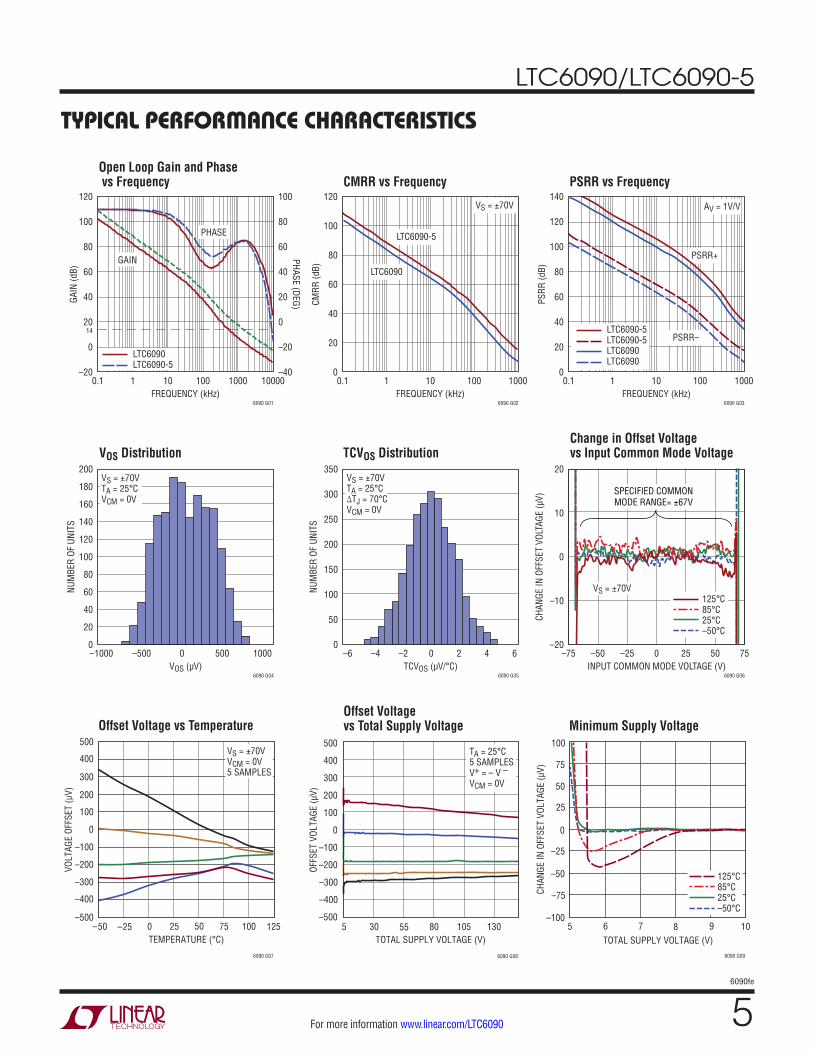
TYPICAL PERFORMANCE CHARACTERISTICS
FREQUENCY (kHz)
CMRR
(dB)
6090 G02
120
80
0
20
40
60
100
0.1 1000101 100
VS = ±70V
LTC6090-5
LTC6090
LTC6090LTC6090LTC6090-5LTC6090-5
FREQUENCY (kHz)
PSRR
(dB)
6090 G03
140
120
60
0
20
40
100
80
0.1 1000101 100
PSRR–
PSRR+
AV = 1V/V
FREQUENCY (kHz)
GAIN
(dB)
PHASE (DEG)
6090 G01
120
100
40
–20
14
0
20
80
60
100
40
–40
–20
0
20
80
60
0.1 10000100101 1000
PHASE
GAIN
LTC6090-5LTC6090
TCVOS (µV/°C)
NUM
BER
OF U
NITS
6090 G05
350
200
0
50
100
150
300
250
–6 –4 20–2 64
VS = ±70VTA = 25°C∆TJ = 70°CVCM = 0V
INPUT COMMON MODE VOLTAGE (V)
CHAN
GE IN
OFF
SET
VOLT
AGE
(µV)
6090 G06
20
–20
–10
0
10
–75 0–25–50 755025
SPECIFIED COMMONMODE RANGE= ±67V
VS = ±70V125°C85°C25°C–50°C
TEMPERATURE (°C)–50
–500
VOLT
AGE
OFFS
ET (µ
V)
–400
–200
–100
0
500
200
0 50 75 100
6090 G07
–300
300
400
100
–25 25 125
VS = ±70VVCM = 0V5 SAMPLES
TOTAL SUPPLY VOLTAGE (V)5
–500
OFFS
ET V
OLTA
GE (µ
V)
–300
–100
100
30 55 80 105
6090 G08
130
300
500
–400
–200
0
200
400TA = 25°C5 SAMPLESV+ = – V –VCM = 0V
TOTAL SUPPLY VOLTAGE (V)5
CHAN
GE IN
OFF
SET
VOLT
AGE
(µV)
–25
0
25
8 10
6090 G09
–50
–75
–1006 7 9
50
75
100
125°C85°C25°C–50°C
VOS (µV)
NUM
BER
OF U
NITS
6090 G04
200
120
100
0
20
40
80
60
180
160
140
–1000 10005000–500
VS = ±70VTA = 25°CVCM = 0V
Open Loop Gain and Phase vs Frequency CMRR vs Frequency PSRR vs Frequency
VOS Distribution TCVOS DistributionChange in Offset Voltage vs Input Common Mode Voltage
Offset Voltage vs TemperatureOffset Voltage vs Total Supply Voltage Minimum Supply Voltage
LTC6090/LTC6090-5
66090fe
For more information www.linear.com/LTC6090
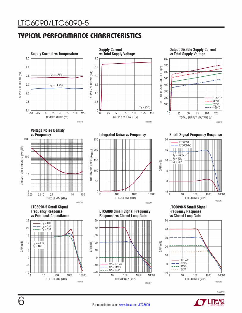
TYPICAL PERFORMANCE CHARACTERISTICS
FREQUENCY (kHz)
10
VOLT
AGE
NOIS
E DE
NSIT
Y (n
V/√H
z)
100
0.001 0.1 1 10010
6090 G13
10.010
1000
FREQUENCY (kHz)10
0
INTE
GRAT
ED N
OISE
(µV R
MS)
150
200
250
100 1000 10000
6090 G14
100
50
FREQUENCY (kHz)
GAIN
(dB)
6090 G15
20
–5
5
0
15
10
1 10000100010010
LTC6090LTC6090-5
RF = 40.2kRI = 10kCF = 2pF
FREQUENCY (kHz)
GAIN
(dB)
6090 G16
25
20
–10
5
0
–5
15
10
1 10000100010010
RF = 40.2kRI = 10k
CF = 2pFCF = 1pFCF = 0pF
FREQUENCY (kHz)
0
GAIN
(dB) 20
40
50
1 100 1000 10000
6090 G17
–2010
30
10
–10 AV = 101V/VAV = 11V/VAV = 1V/V
FREQUENCY (kHz)
GAIN
(dB)
6090 G18
50
–10
40
20
10
30
0
1 10000100010010
5V/V11V/V33V/V101V/V
TEMPERATURE (°C)–50
SUPP
LY C
URRE
NT (m
A)
2.8
2.9
3.0
25 75
6090 G10
2.7
2.6
–25 0 50 100 125
2.5
2.4
VS = ±70V
VS = ±4.75V
SUPPLY VOLTAGE (V)0
0
SUPP
LY C
URRE
NT (m
A)
0.5
1.0
1.5
2.0
3.0
25 50 75 100
6090 G11
125 150
2.5
TA = 25°C
TOTAL SUPPLY VOLTAGE (V)0
OUTP
UT D
ISAB
LE C
URRE
NT (µ
A)
400
6090 G12
200
050 10025 75 125
600
800
300
100
500
700
125°C85°C25°C–50°C
Integrated Noise vs Frequency Small Signal Frequency Response
LTC6090-5 Small Signal Frequency Response vs Feedback Capacitance
LTC6090 Small Signal Frequency Response vs Closed Loop Gain
LTC6090-5 Small Signal Frequency Response vs Closed Loop Gain
Voltage Noise Density vs Frequency
Supply Current vs TemperatureSupply Current vs Total Supply Voltage
Output Disable Supply Current vs Total Supply Voltage
LTC6090/LTC6090-5
76090fe
For more information www.linear.com/LTC6090
TYPICAL PERFORMANCE CHARACTERISTICS
FREQUENCY (kHz)
0.1
OUTP
UT IM
PEDA
CNE
(Ω)
1
10
100
1000
1 100 1000 100000
6090 G19
0.0110 10000
AV = 101V/VAV = 11V/VAV = 1V/V
FREQUENCY (kHz)1
1
OUTP
UT IM
PEDA
NCE
(kΩ
)10
100
1000
10 100
6091 G20
1000
CL = 10pF
COMMON MODE VOLTAGE (V)
10
INPU
T BI
AS C
URRE
NT (|
pA|)
100
–80 0 40
6090 G21
1
–40–60 20 60–20 80
125°CVS = ±70V
100°C
80°C
50°C
DIRECTION OF THE CURRENTIS OUT OF THE PIN
25°C
5°C0.1
1000
10000
COMMON MODE VOLTAGE (V)
1
INPU
T BI
AS C
URRE
NT (|
pA|)
100
1000
–15 5 15
6090 G22
0.1–5–10 100
10
125°C
100°C
VS = ±15V
50°C
25°C
85°C
DIRECTION OF THE CURRENTIS OUT OF THE PIN
OUTP
UT, I
NPUT
(V)
0
20
40
6090 G23
–20
–40
–805µs/DIV
–60
80
60
INPUT
OUTPUT
AV = –10V/VVS = ±70V
OUTP
UT, I
NPUT
(V)
0
20
40
6090 G24
–20
–40
–805µs/DIV
–60
80
60
INPUT
OUTPUT
AV = –10V/VVS = ±70VRF = 100kΩRI = 10kΩCF = 2pF
INPUT50mV/DIV
OUTPUT50mV/DIV
6090 G161µs/DIV
AV = 1V/V
INPU
T ST
EP (0
.5V/
DIV)
OUTPUT STEP (20mV/DIV)
500ns/DIV 6090 G26
AV = 1V/V
INPUT
OUTPUT
INPU
T ST
EP (0
.5V/
DIV)
OUTPUT STEP (20mV/DIV)
500ns/DIV 6090 G27
AV = 1V/V
INPUT
OUTPUT
LTC6090-5 Large Signal Transient Response
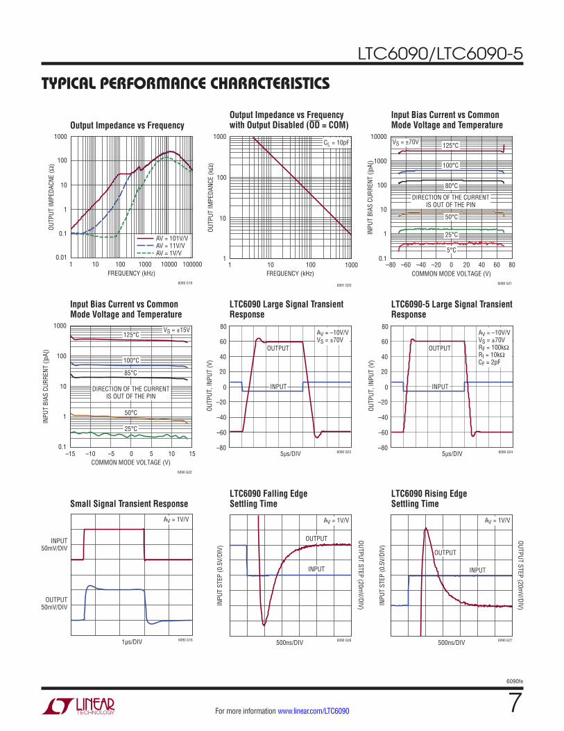
Small Signal Transient ResponseLTC6090 Falling Edge Settling Time
LTC6090 Rising Edge Settling Time
Input Bias Current vs Common Mode Voltage and Temperature
Input Bias Current vs Common Mode Voltage and Temperature
LTC6090 Large Signal Transient Response
Output Impedance vs FrequencyOutput Impedance vs Frequency with Output Disabled (OD = COM)
LTC6090/LTC6090-5
86090fe
For more information www.linear.com/LTC6090
TYPICAL PERFORMANCE CHARACTERISTICS
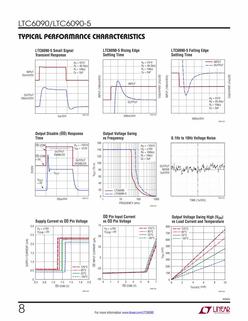
0.1Hz to 10Hz Voltage Noise
Supply Current vs OD Pin VoltageOD Pin Input Current vs OD Pin Voltage
Output Voltage Swing High (VOH) vs Load Current and Temperature
LTC6090-5 Falling Edge Settling Time
Output Disable (OD) Response Time
Output Voltage Swing vs Frequency
LTC6090-5 Small Signal Transient Response
LTC6090-5 Rising Edge Settling Time
1µs/DIV
INPUT25mV/DIV
OUTPUT100mV/DIV
6090 G28
AV = 5V/VRF = 40.2kΩRI = 10kΩCF = 2pF
500ns/DIV
INPU
T (1
00m
V/DI
V)
OUTPUT (50mV/DIV)
6090 G29
AV = 5V/VRF = 40.2kΩRI = 10kΩCF = 2pF
INPUT
OUTPUT
500ns/DIV
INPU
T (1
00m
V/DI
V)
OUTPUT (50mV/DIV)
6090 G30
INPUTOUTPUT
AV = 5V/VRF = 40.2kΩRI = 10kΩCF = 2pF
6090 G3120µs/DIV
OD-COM
OD-COM= 0V
2V/D
IV
OUTPUTENABLED
OUTPUTDISABLED
VOUT = 0V
AV = –10V/VVIN = –0.5V
VOUT
FREQUENCY (kHz)
V OUT
(VP-
P)
6090 G32
160
0
140
100
80
60
40
120
20
1 100010010
LTC6090-5LTC6090
AV = –10V/VVS = ±70VRF = 100kΩRI = 10kΩCF = 2pF
TIME (1s/DIV)
OUTPUTNOISE
2µV/DIV
6090 G33
OD-COM (V)0.5
0
SUPP
LY C
URRE
NT (m
A)
0.5
1.0
1.5
2.0
3.0
0.8 1.0 1.3 1.5
6090 G34
1.8 2.0
2.5
125°C85°C25°C–50°C
VS = ±70VVCOM = 0V
OD-COM (V)0 1
–50
OD IN
PUT
CURR
ENT
(µA)
0
–25
2 6
75
50
25
3 4 5 7
6090 G35
125°C85°C25°C–50°C
VS = ±70VVCOM = 0V
ISOURCE (mA)0
V OH
(mV)
300
400
500
6 10
6090 G36
200
100
02 4 8
600
700
800125°C85°C25°C–50°C
LTC6090/LTC6090-5
96090fe
For more information www.linear.com/LTC6090
TYPICAL PERFORMANCE CHARACTERISTICS
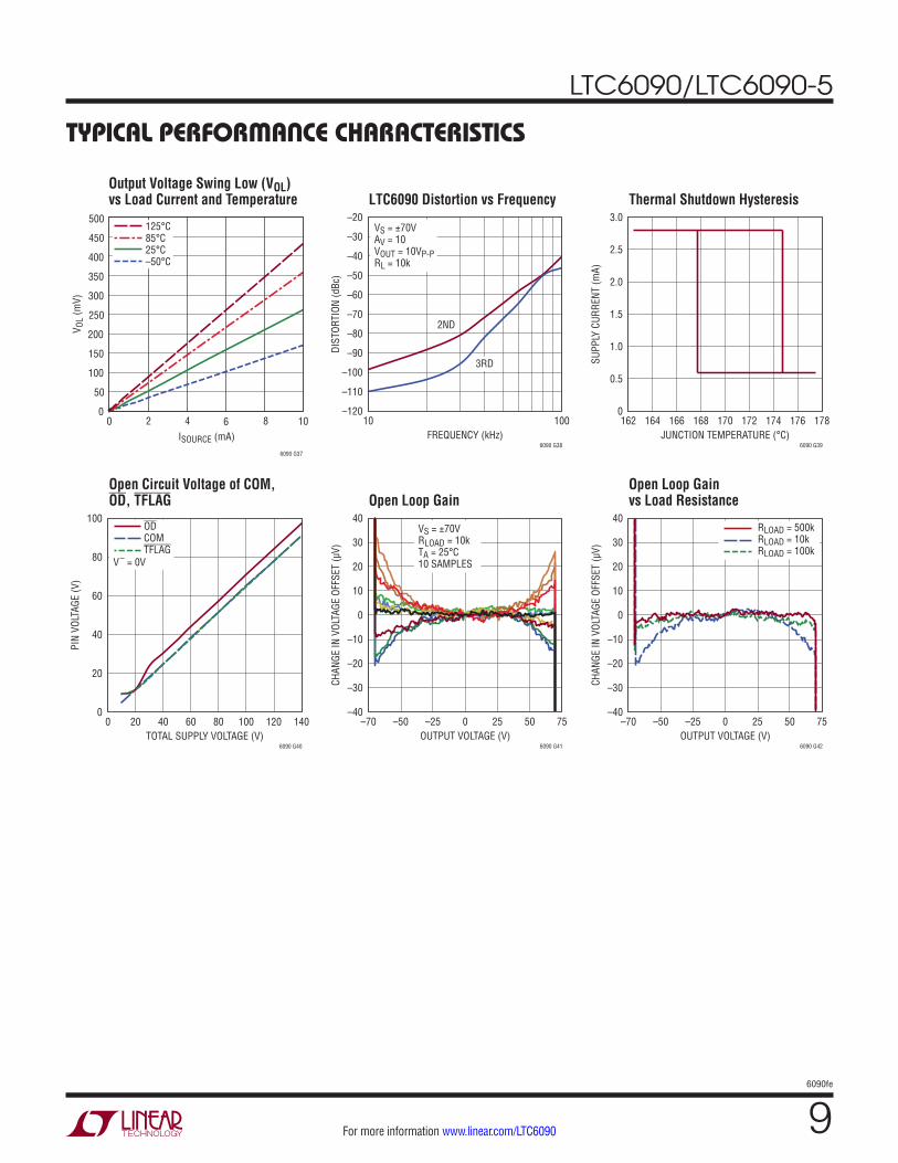
Output Voltage Swing Low (VOL) vs Load Current and Temperature
Open Circuit Voltage of COM, OD, TFLAG
LTC6090 Distortion vs Frequency
Open Loop Gain
Thermal Shutdown Hysteresis
Open Loop Gain vs Load Resistance
ISOURCE (mA)0
V OL
(mV)
150
200
250
6 10
6090 G37
100
50
02 4 8
300
400
350
500
450125°C85°C25°C–50°C
FREQUENCY (kHz)
DIST
ORTI
ON (d
Bc)
6090 G38
–20
–120
–110
–100
–90
–50
–40
–30
–80
–70
–60
10 100
VS = ±70VAV = 10VOUT = 10VP-PRL = 10k
2ND
3RD
JUNCTION TEMPERATURE (°C)
SUPP
LY C
URRE
NT (m
A)
6090 G39
3.0
0
0.5
1.0
2.5
2.0
1.5
162 178170166164 168 176174172
TOTAL SUPPLY VOLTAGE (V)
PIN
VOLT
AGE
(V)
6090 G40
100
0
20
40
80
60
0 140804020 60 120100
ODCOMTFLAG
V– = 0V
OUTPUT VOLTAGE (V)
CHAN
GE IN
VOL
TAGE
OFF
SET
(µV)
6090 G41
40
–40
–30
10
20
30
–20
–10
0
–70 –50 –25 0 25 50 75
VS = ±70VRLOAD = 10kTA = 25°C10 SAMPLES
OUTPUT VOLTAGE (V)
CHAN
GE IN
VOL
TAGE
OFF
SET
(µV)
6090 G42
40
–40
–30
10
20
30
–20
–10
0
–70 –50 –25 0 25 50 75
RLOAD = 100kRLOAD = 10kRLOAD = 500k
LTC6090/LTC6090-5
106090fe
For more information www.linear.com/LTC6090
PIN FUNCTIONSCOM (Pin 1/Pin 1): COM Pin is used to interface OD and TFLAG pins to voltage control circuits. Tie this pin to the low voltage ground, or let it float.
–IN (Pin 2/Pin 4): Inverting Input Pin. Input common mode range is V– + 3V to V+ – 3V. Do not exceed absolute maximum voltage range.
+IN (Pin 3/Pin 5): Noninverting Input Pin. Input common mode range is V– + 3V to V+ – 3V. Do not exceed absolute maximum voltage range.
V– (Pin 4, Exposed Pad Pin 9/Pin 8, Exposed Pad Pin 17): Negative Supply Pin. Connect to V– Only. To achieve low thermal resistance connect this pin to the V– power plane. The V– power plane connection removes heat from the device and should be electrically isolated from all other power planes.
TFLAG (Pins 5, 9/Pins 9, 17): Temperature Flag Pin. The TFLAG pin is an open drain output that sinks current when the die temperature exceeds 145°C.
OUT (Pin 6/Pin 12): Output Pin. If this rail-to-rail output goes below V– , the ESD protection diode will forward bias. If OUT goes above V+, then output device diodes will forward bias. Avoid forward biasing the diodes on the OUT pin. Excessive current can cause damage.
V+ (Pin 7/Pin 14): Positive Supply Pin.
OD (Pin 8/Pin 16): Output Disable Pin. Active low input disables the output stage. If left open, an internal pull-up resistor enables the amplifier. Input voltage levels are referred to the COM pin.
GUARD (NA/Pins 2, 3, 6, 7, 10, 11, 13, 15): Guard pins increase clearance and creepage between other pins. Pins 3 and 6 can be used to build guard rings around the inputs.
(S8E/FE)
LTC6090/LTC6090-5
116090fe
For more information www.linear.com/LTC6090
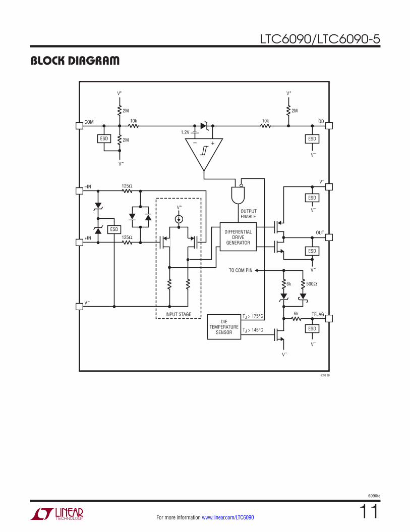
BLOCK DIAGRAM
6090 BD
TJ > 175°C
TJ > 145°C
– +
V+
10k
2M
V+
2M
COM
–IN
+IN
V –
V–
2M
10k
V–
DIFFERENTIALDRIVE
GENERATOR
OUTPUTENABLE
500Ω
V–
V–
V–
6k
TO COM PIN
6k
DIETEMPERATURE
SENSOR
INPUT STAGE
V+
125Ω
125Ω
OD
TFLAG
V+
OUT
V–
ESD
ESD
ESD
ESD
ESD
ESD1.2V
LTC6090/LTC6090-5
126090fe
For more information www.linear.com/LTC6090
General
The LTC6090 high voltage operational amplifier is designed in a Linear Technology proprietary process enabling a rail-to-rail output stage with a 140V supply while maintaining precision, low offset, and low noise.
Power Supply
The LTC6090 works off single or split supplies. Split sup-plies can be balanced or unbalanced. For example, two ±70V supplies can be used, or a 100V and –40V supply can be used. For single supply applications place a high quality surface mount ceramic 0.1µF bypass capacitor between the supply pins close to the part. For dual supply applications use two high quality surface mount ceramic capacitors between V+ to ground, and V– to ground located close to the part. When using split supplies, supply se-quencing does not cause problems.
Input Protection
As shown in the block diagram, the LTC6090 has a com-prehensive protection network to prevent damage to the input devices. The current limiting resistors and back to back diodes are to keep the inputs from being driven apart. The voltage-current relationship combines exponential and resistive until the voltage difference between the pins reach 12V.
At that point the Zeners turn on. Additional current into the pins will snap back the input differential voltage to 9V. In the event of an ESD strike between an input and V–, the voltage clamps and ESD device fire providing a current path to V– protecting the input devices.
The input pin protection is designed to protect against momentary ESD events. A repetitive large fast input swing (>5.5V and <20ns rise time) will cause repeated stress on the MOSFET input devices. When in such an application, anti-parallel diodes (1N4148) should be connected between the inputs to limit the swing.
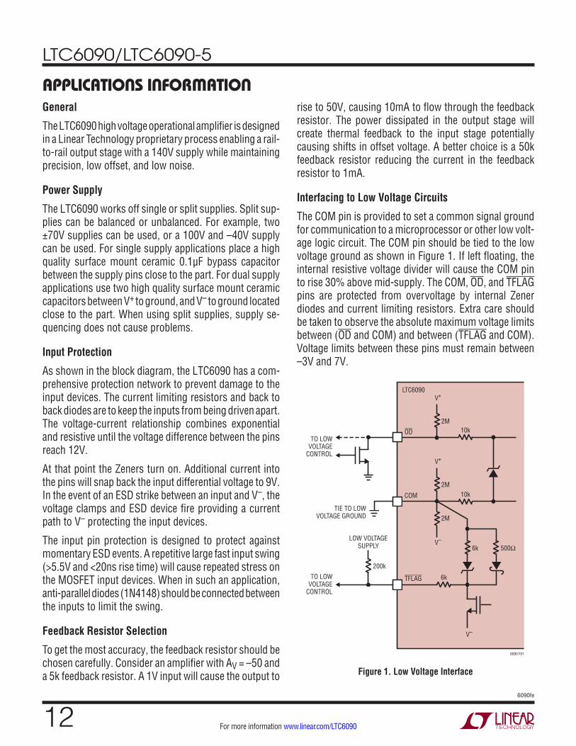
Feedback Resistor Selection
To get the most accuracy, the feedback resistor should be chosen carefully. Consider an amplifier with AV = –50 and a 5k feedback resistor. A 1V input will cause the output to Figure 1. Low Voltage Interface
APPLICATIONS INFORMATIONrise to 50V, causing 10mA to flow through the feedback resistor. The power dissipated in the output stage will create thermal feedback to the input stage potentially causing shifts in offset voltage. A better choice is a 50k feedback resistor reducing the current in the feedback resistor to 1mA.
Interfacing to Low Voltage Circuits
The COM pin is provided to set a common signal ground for communication to a microprocessor or other low volt-age logic circuit. The COM pin should be tied to the low voltage ground as shown in Figure 1. If left floating, the internal resistive voltage divider will cause the COM pin to rise 30% above mid-supply. The COM, OD, and TFLAG pins are protected from overvoltage by internal Zener diodes and current limiting resistors. Extra care should be taken to observe the absolute maximum voltage limits between (OD and COM) and between (TFLAG and COM). Voltage limits between these pins must remain between –3V and 7V.
6090 F01
OD
COM
LTC6090
TFLAG
10k
LOW VOLTAGESUPPLY
TIE TO LOWVOLTAGE GROUND
TO LOWVOLTAGE
CONTROL
TO LOWVOLTAGE
CONTROL
6k
200k
V+
V–
V–
2M
V+
2M
2M
10k
6k 500Ω
LTC6090/LTC6090-5
136090fe
For more information www.linear.com/LTC6090
APPLICATIONS INFORMATION
Figure 2. Starting Up
Figure 3. LTC6090 Output Disable Function
1ms/DIV6090 F02
OUT10V/DIV
V+
2.5ms/DIV6090 F03
OUT2V/DIV
OD2V/DIV
Output Disable
The OD pin is an active low disable with an internal 2MΩ resistor that will pull up the OD pin enabling the output stage if left open. The OD pin voltage is limited by an internal Zener diode. When the OD pin is brought low to within 0.65V of the COM pin, the output stage is disabled, leaving the bias and input circuits enabled. This results in 580μA (typical) standby current through the device. The OD pin can be directly connected to the low voltage logic or an open drain NMOS device as shown in Figure 1.
For simplest shutdown operation, float the COM pin, and tie the OD pin to the TFLAG pin. This will float the low voltage control pins, and the overtemperature circuit will safely shutdown the output stage if the die temperature reaches 145°C.
Extra care should be taken to observe the absolute maxi-mum voltage limits between (OD and COM) and between (TFLAG and COM). Voltage limits between these pins must remain between –3V and 7V.
When coming out of shutdown the LTC6090 bias circuits and input stage are already powered up leaving only the output stage to turn on and drive to the proper output voltage. Figures 2 and 3 show the part starting up and coming out of shutdown, respectively.
Thermal Shutdown
The TFLAG pin is an open drain output pin that sinks 200µA (typical) when the die temperature exceeds 145°C. The temperature sensor has 5°C of hysteresis requiring the part to cool to 140°C before disabling the TFLAG pin. Extra care should be taken to observe the absolute maximum voltage limits between (OD and COM) and between (TFLAG and COM). Voltage limits between these pins must remain between –3V and 7V.
Tying the the TFLAG pin to the OD pin will automatically shut down the output stage as shown in Figure 4. This will ensure the junction temperature does not exceed 150°C.
For safety, an independent second overtemperature threshold shuts down the output stage if the internal die temperature rises to 175°C. There is hysteresis in the thermal shutdown circuit requiring the die temperature to cool 7°C. Once the device has cooled sufficiently, the output stage will enable. Degradation can occur or reli-ability may be affected when the junction temperature of the device exceeds 150°C.
Figure 4. Automatic Thermal Output Disable Using the TFLAG Pin
6090 F04
OD
TFLAG
10k
COMOPTIONAL(CAN BE LEFT
FLOATING)
6k
V+
V–
2M
LTC6090
LTC6090/LTC6090-5
146090fe
For more information www.linear.com/LTC6090
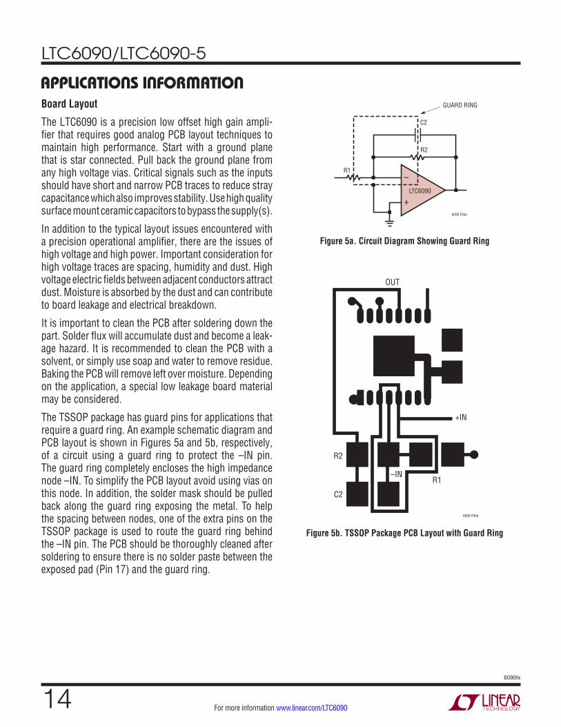
APPLICATIONS INFORMATIONBoard Layout
The LTC6090 is a precision low offset high gain ampli-fier that requires good analog PCB layout techniques to maintain high performance. Start with a ground plane that is star connected. Pull back the ground plane from any high voltage vias. Critical signals such as the inputs should have short and narrow PCB traces to reduce stray capacitance which also improves stability. Use high quality surface mount ceramic capacitors to bypass the supply(s).
In addition to the typical layout issues encountered with a precision operational amplifier, there are the issues of high voltage and high power. Important consideration for high voltage traces are spacing, humidity and dust. High voltage electric fields between adjacent conductors attract dust. Moisture is absorbed by the dust and can contribute to board leakage and electrical breakdown.
It is important to clean the PCB after soldering down the part. Solder flux will accumulate dust and become a leak-age hazard. It is recommended to clean the PCB with a solvent, or simply use soap and water to remove residue. Baking the PCB will remove left over moisture. Depending on the application, a special low leakage board material may be considered.
The TSSOP package has guard pins for applications that require a guard ring. An example schematic diagram and PCB layout is shown in Figures 5a and 5b, respectively, of a circuit using a guard ring to protect the –IN pin. The guard ring completely encloses the high impedance node –IN. To simplify the PCB layout avoid using vias on this node. In addition, the solder mask should be pulled back along the guard ring exposing the metal. To help the spacing between nodes, one of the extra pins on the TSSOP package is used to route the guard ring behind the –IN pin. The PCB should be thoroughly cleaned after soldering to ensure there is no solder paste between the exposed pad (Pin 17) and the guard ring.
6090 F05a
–
+LTC6090
R2
C2
R1
GUARD RING
Figure 5a. Circuit Diagram Showing Guard Ring
Figure 5b. TSSOP Package PCB Layout with Guard Ring
6090 F05b
R2
C2
R1–IN
+IN
OUT
LTC6090/LTC6090-5
156090fe
For more information www.linear.com/LTC6090
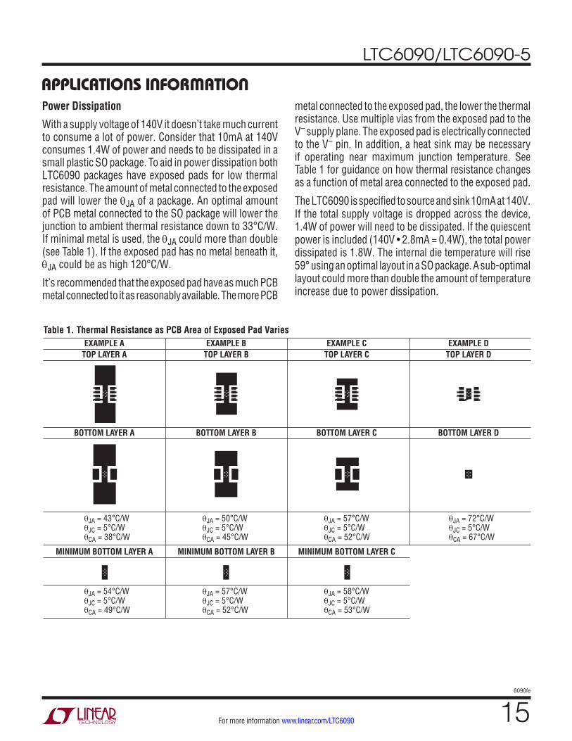
APPLICATIONS INFORMATIONPower Dissipation
With a supply voltage of 140V it doesn’t take much current to consume a lot of power. Consider that 10mA at 140V consumes 1.4W of power and needs to be dissipated in a small plastic SO package. To aid in power dissipation both LTC6090 packages have exposed pads for low thermal resistance. The amount of metal connected to the exposed pad will lower the θJA of a package. An optimal amount of PCB metal connected to the SO package will lower the junction to ambient thermal resistance down to 33°C/W. If minimal metal is used, the θJA could more than double (see Table 1). If the exposed pad has no metal beneath it, θJA could be as high 120°C/W.
It’s recommended that the exposed pad have as much PCB metal connected to it as reasonably available. The more PCB
TOP LAYER A TOP LAYER B TOP LAYER C TOP LAYER DEXAMPLE A EXAMPLE B EXAMPLE C EXAMPLE D
BOTTOM LAYER A
θJA = 43°C/WθJC = 5°C/WθCA = 38°C/W
θJA = 50°C/WθJC = 5°C/WθCA = 45°C/W
θJA = 57°C/WθJC = 5°C/WθCA = 52°C/W
θJA = 54°C/WθJC = 5°C/WθCA = 49°C/W
θJA = 57°C/WθJC = 5°C/WθCA = 52°C/W
θJA = 58°C/WθJC = 5°C/WθCA = 53°C/W
θJA = 72°C/WθJC = 5°C/WθCA = 67°C/W
BOTTOM LAYER B BOTTOM LAYER C
MINIMUM BOTTOM LAYER A MINIMUM BOTTOM LAYER B MINIMUM BOTTOM LAYER C
BOTTOM LAYER D
Table 1. Thermal Resistance as PCB Area of Exposed Pad Varies
metal connected to the exposed pad, the lower the thermal resistance. Use multiple vias from the exposed pad to the V– supply plane. The exposed pad is electrically connected to the V– pin. In addition, a heat sink may be necessary if operating near maximum junction temperature. See Table 1 for guidance on how thermal resistance changes as a function of metal area connected to the exposed pad.
The LTC6090 is specified to source and sink 10mA at 140V. If the total supply voltage is dropped across the device, 1.4W of power will need to be dissipated. If the quiescent power is included (140V • 2.8mA = 0.4W), the total power dissipated is 1.8W. The internal die temperature will rise 59° using an optimal layout in a SO package. A sub-optimal layout could more than double the amount of temperature increase due to power dissipation.
LTC6090/LTC6090-5
166090fe
For more information www.linear.com/LTC6090
APPLICATIONS INFORMATIONIn order to avoid damaging the device, the absolute maximum junction temperature should not be exceeded (TJMAX = 150°C). Junction temperature is determined using the expression:
TJ = PD • θJA + TA
where PD is the power dissipated in the package, θJA is the package thermal resistance from ambient to junction and TA is the ambient temperature. For example, if the part has a 140V supply voltage with 2.8mA of quiescent current and the output is 20V above the negative rail sourcing 10mA, the total power dissipated in the device is (120V • 10mA) + (140V • 2.8mA) = 1.6W. Under these conditions the ambient temperature should not exceed:
TA = TJMAX – (PD • θJA) = 150°C – (1.6W • 33°C/W) = 97°C.
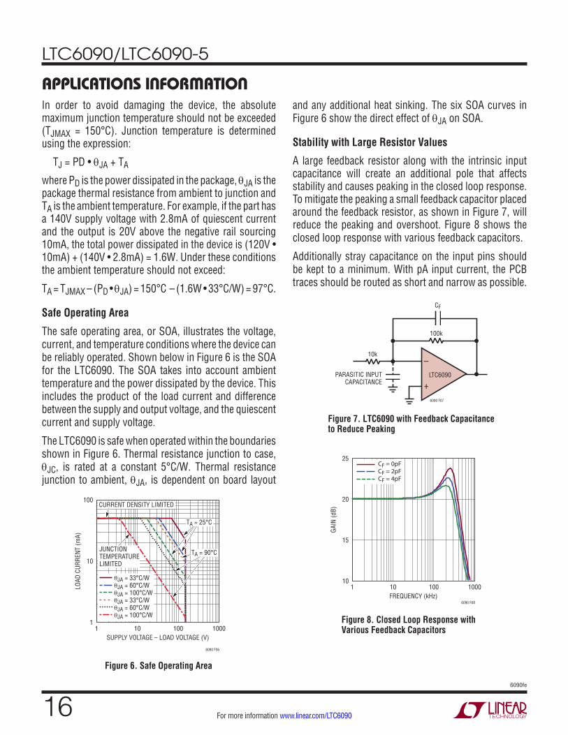
Safe Operating Area
The safe operating area, or SOA, illustrates the voltage, current, and temperature conditions where the device can be reliably operated. Shown below in Figure 6 is the SOA for the LTC6090. The SOA takes into account ambient temperature and the power dissipated by the device. This includes the product of the load current and difference between the supply and output voltage, and the quiescent current and supply voltage.
The LTC6090 is safe when operated within the boundaries shown in Figure 6. Thermal resistance junction to case, θJC, is rated at a constant 5°C/W. Thermal resistance junction to ambient, θJA, is dependent on board layout
Figure 8. Closed Loop Response with Various Feedback Capacitors
Figure 7. LTC6090 with Feedback Capacitance to Reduce Peaking
Figure 6. Safe Operating Area
6090 F07
–
+LTC6090
100k
CF
10k
PARASITIC INPUTCAPACITANCE
JUNCTION TEMPERATURE LIMITED
SUPPLY VOLTAGE – LOAD VOLTAGE (V)
LOAD
CUR
RENT
(mA)
6090 F06
100
10
1101 1000100
CURRENT DENSITY LIMITED
θJA = 33°C/WθJA = 60°C/WθJA = 100°C/WθJA = 33°C/WθJA = 60°C/WθJA = 100°C/W
TA = 25°C
TA = 90°C
FREQUENCY (kHz)
GAIN
(dB)
6090 F08
25
20
15
101 100010010
CF = 4pFCF = 2pFCF = 0pF
and any additional heat sinking. The six SOA curves in Figure 6 show the direct effect of θJA on SOA.
Stability with Large Resistor Values
A large feedback resistor along with the intrinsic input capacitance will create an additional pole that affects stability and causes peaking in the closed loop response. To mitigate the peaking a small feedback capacitor placed around the feedback resistor, as shown in Figure 7, will reduce the peaking and overshoot. Figure 8 shows the closed loop response with various feedback capacitors.
Additionally stray capacitance on the input pins should be kept to a minimum. With pA input current, the PCB traces should be routed as short and narrow as possible.
LTC6090/LTC6090-5
176090fe
For more information www.linear.com/LTC6090
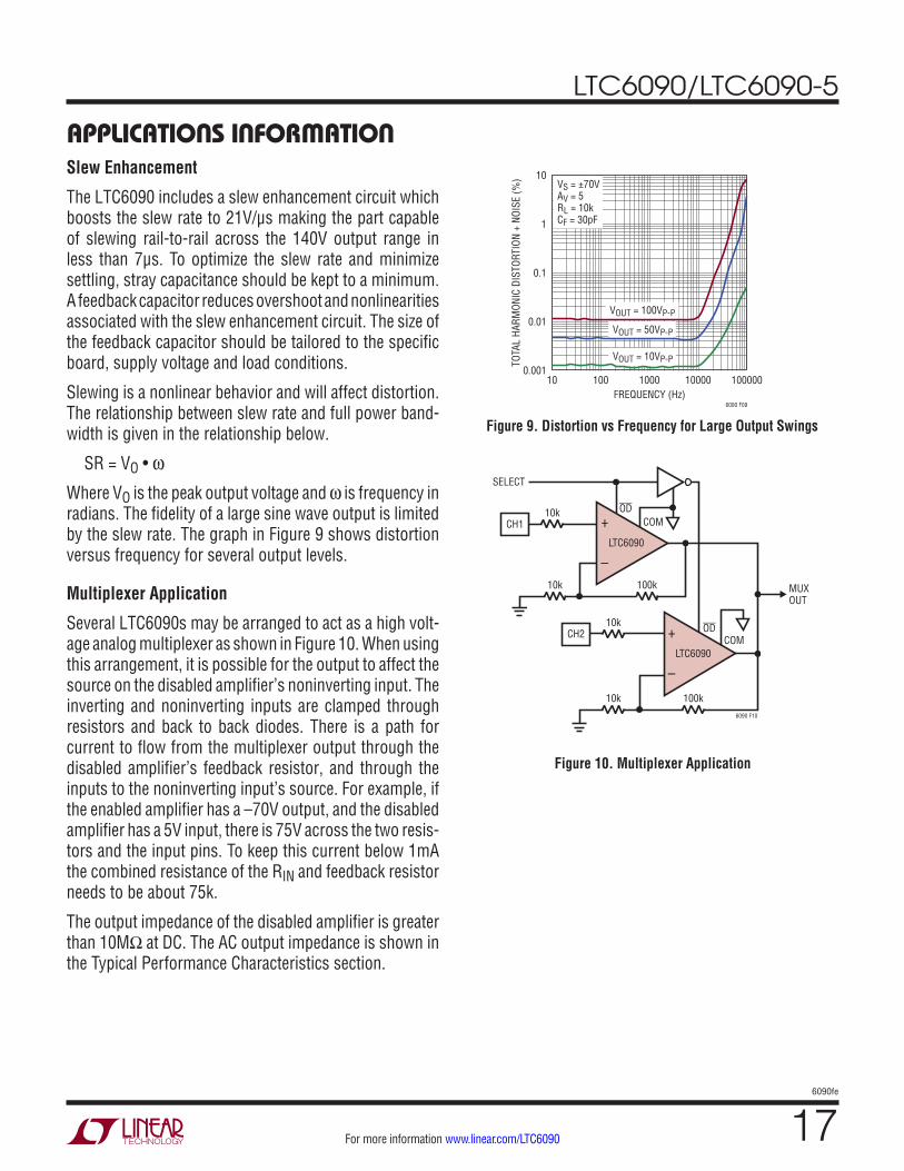
APPLICATIONS INFORMATIONSlew Enhancement
The LTC6090 includes a slew enhancement circuit which boosts the slew rate to 21V/μs making the part capable of slewing rail-to-rail across the 140V output range in less than 7μs. To optimize the slew rate and minimize settling, stray capacitance should be kept to a minimum. A feedback capacitor reduces overshoot and nonlinearities associated with the slew enhancement circuit. The size of the feedback capacitor should be tailored to the specific board, supply voltage and load conditions.
Slewing is a nonlinear behavior and will affect distortion. The relationship between slew rate and full power band-width is given in the relationship below.
SR = VO • ω
Where VO is the peak output voltage and ω is frequency in radians. The fidelity of a large sine wave output is limited by the slew rate. The graph in Figure 9 shows distortion versus frequency for several output levels.
Multiplexer Application
Several LTC6090s may be arranged to act as a high volt-age analog multiplexer as shown in Figure 10. When using this arrangement, it is possible for the output to affect the source on the disabled amplifier’s noninverting input. The inverting and noninverting inputs are clamped through resistors and back to back diodes. There is a path for current to flow from the multiplexer output through the disabled amplifier’s feedback resistor, and through the inputs to the noninverting input’s source. For example, if the enabled amplifier has a –70V output, and the disabled amplifier has a 5V input, there is 75V across the two resis-tors and the input pins. To keep this current below 1mA the combined resistance of the RIN and feedback resistor needs to be about 75k.
The output impedance of the disabled amplifier is greater than 10MΩ at DC. The AC output impedance is shown in the Typical Performance Characteristics section.
Figure 10. Multiplexer Application
Figure 9. Distortion vs Frequency for Large Output Swings
FREQUENCY (Hz)
TOTA
L HA
RMON
IC D
ISTO
RTIO
N +
NOIS
E (%
)
6090 F09
10
0.1
1
0.01
0.00110 100000100 1000 10000
VS = ±70VAV = 5RL = 10kCF = 30pF
VOUT = 100VP-P
VOUT = 50VP-P
VOUT = 10VP-P
6090 F10
CH110k OD
OD10k
10k 100k
10k 100k
CH2
SELECT
–
+
–
+LTC6090
LTC6090
COM
MUXOUT
COM
LTC6090/LTC6090-5
186090fe
For more information www.linear.com/LTC6090
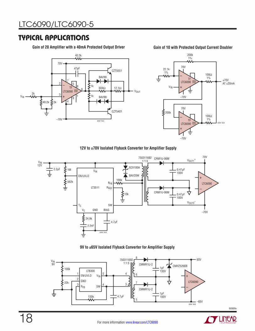
TYPICAL APPLICATIONSGain of 20 Amplifier with a 40mA Protected Output Driver Gain of 10 with Protected Output Current Doubler
12V to ±70V Isolated Flyback Converter for Amplifier Supply
6090 TA04
LT3511
VIN
VIN12V
VC GND BIAS
RFB
RREF
SWTC
2.2nF
24.9k
10k
BAV20W
BZX100A
EN/UVLO
4.7µF
100k
1M
562k
• CRM1U-06M
CRM1U-06M
0.47µF100V
0.47µF100V
2.2µF
VOUT1+
VOUT2–
+
–LTC6090
70V
–70V
•
•
7503116921:1:5
6090 TA05
VIN9V
100k
22k
• CMMR1U-2
7503116921:1:5 CMMR1U-2 CMHZ5266B
1µF100V
1µF130V
+
–LTC6090
65V
–65V
•
•
5
4
1
2
3
4.7µF
4
3
130k
EN/UVLO
GND
RFB
VIN
SW
LT8300
8
6
7
5
9V to ±65V Isolated Flyback Converter for Amplifier Supply
6090 TA03
–
+LTC6090
70V
–70V
200k1%
200k
TFOD
22.1k1%
VIN
100Ω1%
–
+LTC6090
70V
–70V
TFOD
100Ω1%
±70VAT ±20mA
6090 TA02
–
+
604Ω68
1
57
4
2
39
47pF
BAV99
BAV99
LTC6090
70V
–70V
12.1Ω
40.2k
TFOD VOUT
CZT5401
1k
1k
CZT5551
2k
2k40.2k
VIN
LTC6090/LTC6090-5
196090fe
For more information www.linear.com/LTC6090
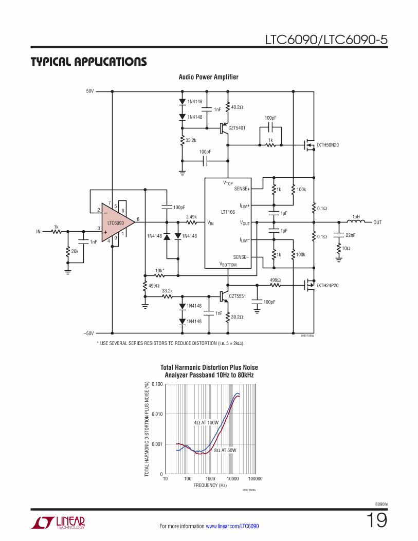
TYPICAL APPLICATIONSAudio Power Amplifier
FREQUENCY (Hz)
TOTA
L HA
RMON
IC D
ISTO
RTIO
N PL
US N
OISE
(%)
6090 TA06b
0.100
0
0.001
0.010
10 100 100000100001000
8Ω AT 50W
4Ω AT 100W
Total Harmonic Distortion Plus NoiseAnalyzer Passband 10Hz to 80kHz
LT1166
VTOPSENSE+
VBOTTOM
SENSE–
VIN VOUT
ILIM+
100k
1k
100pF
ILIM–
–
+LTC6090
100pF
100k10Ω
1k
0.1Ω
IXTH50N20
IXTH24P20
6090 TA06a
OUT
0.1Ω
33.2k
40.2Ω1nF
2.49k
1k
CZT5551
1N4148
CZT5401
1N4148
* USE SEVERAL SERIES RESISTORS TO REDUCE DISTORTION (i.e. 5 × 2kΩ).
33.2k
10k*
1nF
100pF
1N41481N4148
39.2Ω
20k
IN
499Ω
4
499Ω
1nF9
1
75
8
6
2
3
–50V
50V
100pF
1k
1µF
1µF
1N4148
1N4148
22nF
1µH
LTC6090/LTC6090-5
206090fe
For more information www.linear.com/LTC6090
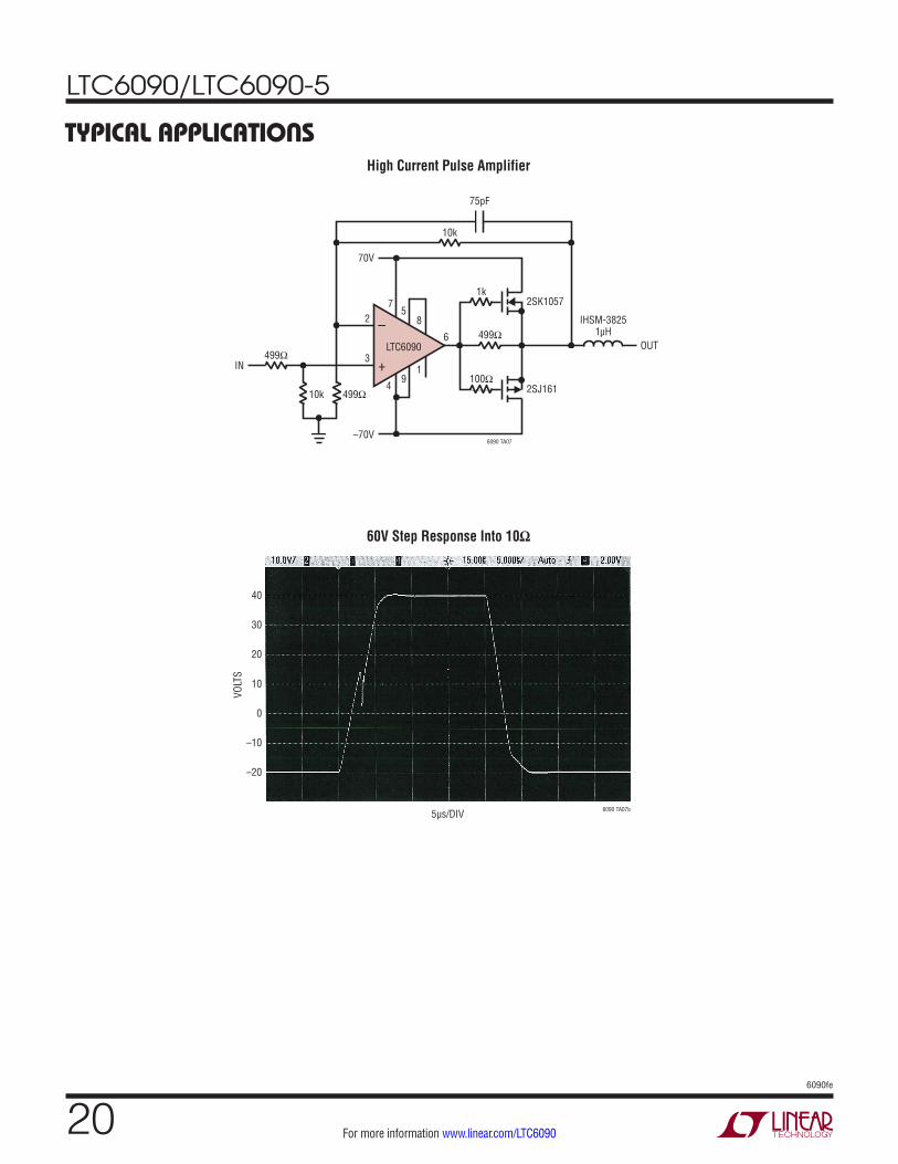
TYPICAL APPLICATIONSHigh Current Pulse Amplifier
60V Step Response Into 10Ω
5µs/DIV
VOLT
S
6090 TA07b
10
20
30
–20
–10
0
40
–
+LTC6090
6090 TA07
OUT499Ω
499Ω
10k
IN
49
1
75
6
82
3
499Ω
–70V
70V
2SK1057
2SJ161
10k
75pF
1k
100Ω
IHSM-38251µH
LTC6090/LTC6090-5
216090fe
For more information www.linear.com/LTC6090
–
+LTC6090
6090 TA08a
OUT499Ω
10k
IN
49
6
1
75
82
3
100Ω
100nF
100nF
499Ω
–50V
50V
2SK1057
2SJ1612SJ161
2k 2k 2k
50pF
2k 2k
IHSM-38251µH
2SK1057
100Ω
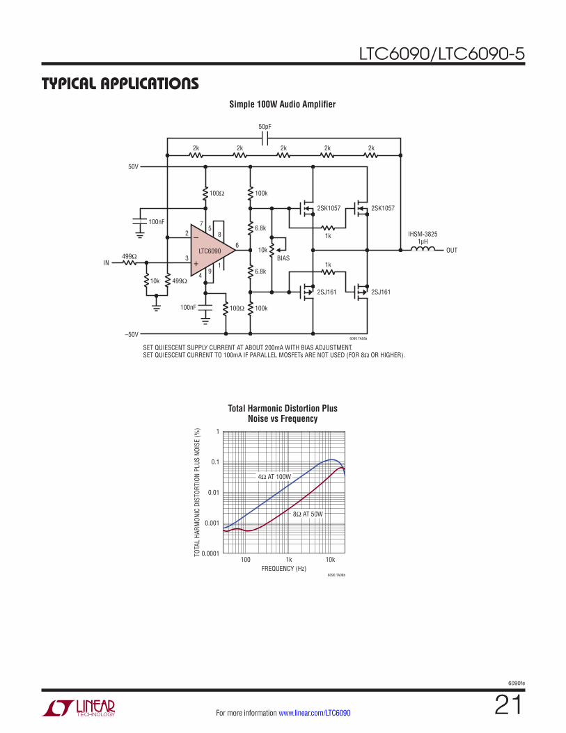
SET QUIESCENT SUPPLY CURRENT AT ABOUT 200mA WITH BIAS ADJUSTMENT.SET QUIESCENT CURRENT TO 100mA IF PARALLEL MOSFETs ARE NOT USED (FOR 8Ω OR HIGHER).
100k
100k
6.8k
BIAS10k
6.8k
1k
1k
FREQUENCY (Hz)
TOTA
L HA
RMON
IC D
ISTO
RTIO
N PL
US N
OISE
(%)
6090 TA08b
1
0.0001
0.001
0.01
0.1
10k1k100
8Ω AT 50W
4Ω AT 100W
TYPICAL APPLICATIONSSimple 100W Audio Amplifier
Total Harmonic Distortion PlusNoise vs Frequency
LTC6090/LTC6090-5
226090fe
For more information www.linear.com/LTC6090
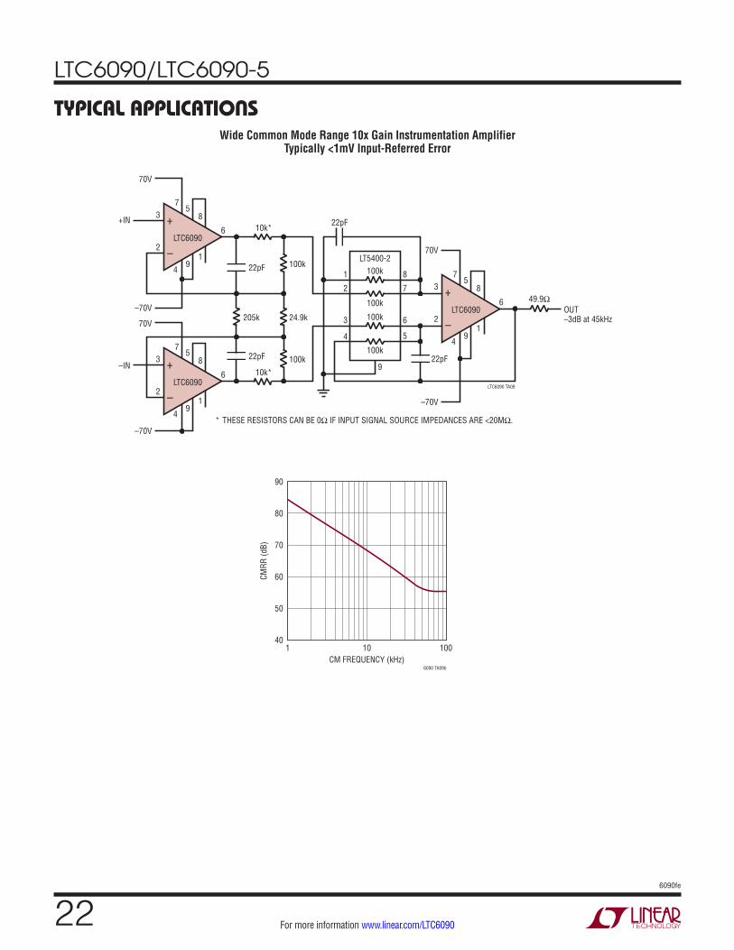
TYPICAL APPLICATIONSWide Common Mode Range 10x Gain Instrumentation Amplifier
Typically <1mV Input-Referred Error
+
–LTC6090
205k
10k*
22pF49
6
1
75
83
2
+
–LTC6090
49
6
1
75
83
2
24.9k
100k
100k
–70V
70V
–70V
70V
* THESE RESISTORS CAN BE 0Ω IF INPUT SIGNAL SOURCE IMPEDANCES ARE <20MΩ.
22pF
10k*
+
–LTC6090
100kLT5400-2
100k
100k
100k4
9
6
1
75
83
2
1
2
3
4
8
7
6
5
922pF
22pF+IN
–IN
70V
–70V
LTC6090 TA09
49.9ΩOUT–3dB at 45kHz
CM FREQUENCY (kHz)
CMRR
(dB)
6090 TA09b
90
40
50
60
70
80
1 10 100
LTC6090/LTC6090-5
236090fe
For more information www.linear.com/LTC6090
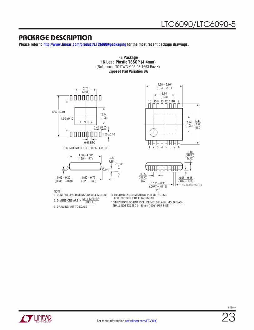
PACKAGE DESCRIPTIONPlease refer to http://www.linear.com/product/LTC6090#packaging for the most recent package drawings.
FE16 (BA) TSSOP REV K 0913
0.09 – 0.20(.0035 – .0079)
0° – 8°
0.25REF
0.50 – 0.75(.020 – .030)
4.30 – 4.50*(.169 – .177)
1 3 4 5 6 7 8
10 9
4.90 – 5.10*(.193 – .201)
16 1514 13 12 11
1.10(.0433)
MAX
0.05 – 0.15(.002 – .006)
0.65(.0256)
BSC
2.74(.108)
2.74(.108)
0.195 – 0.30(.0077 – .0118)
TYP
2
MILLIMETERS(INCHES) *DIMENSIONS DO NOT INCLUDE MOLD FLASH. MOLD FLASH
SHALL NOT EXCEED 0.150mm (.006") PER SIDE
NOTE:1. CONTROLLING DIMENSION: MILLIMETERS
2. DIMENSIONS ARE IN
RECOMMENDED SOLDER PAD LAYOUT
3. DRAWING NOT TO SCALE
0.45 ±0.05
0.65 BSC
4.50 ±0.10
6.60 ±0.10
1.05 ±0.10
2.74(.108)
2.74(.108)
SEE NOTE 4
4. RECOMMENDED MINIMUM PCB METAL SIZE FOR EXPOSED PAD ATTACHMENT
6.40(.252)BSC
FE Package16-Lead Plastic TSSOP (4.4mm)
(Reference LTC DWG # 05-08-1663 Rev K)Exposed Pad Variation BA
LTC6090/LTC6090-5
246090fe
For more information www.linear.com/LTC6090
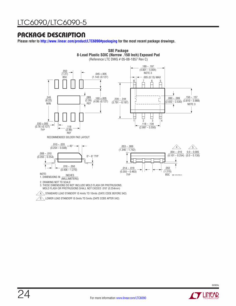
PACKAGE DESCRIPTIONPlease refer to http://www.linear.com/product/LTC6090#packaging for the most recent package drawings.
.016 – .050(0.406 – 1.270)
.010 – .020(0.254 – 0.508)
× 45°
0°– 8° TYP.008 – .010
(0.203 – 0.254)
S8E 1015 REV C
.053 – .069(1.346 – 1.752)
.014 – .019(0.355 – 0.483)
TYP
.004 – .010(0.101 – 0.254)
0.0 – 0.005(0.0 – 0.130)
.080 – .099(2.032 – 2.530)
.118 – .139(2.997 – 3.550)
.050(1.270)
BSC
1 2 3 4
.150 – .157(3.810 – 3.988)
NOTE 3
8 7.005 (0.13) MAX
6 5
.189 – .197(4.801 – 5.004)
NOTE 3
.228 – .244(5.791 – 6.197)
.160 ±.005(4.06 ±0.127)
.118(2.99)REF
RECOMMENDED SOLDER PAD LAYOUT
.045 ±.005(1.143 ±0.127)
.050(1.27)BSC
INCHES(MILLIMETERS)
NOTE:1. DIMENSIONS IN
2. DRAWING NOT TO SCALE3. THESE DIMENSIONS DO NOT INCLUDE MOLD FLASH OR PROTRUSIONS. MOLD FLASH OR PROTRUSIONS SHALL NOT EXCEED .010" (0.254mm)
4. STANDARD LEAD STANDOFF IS 4mils TO 10mils (DATE CODE BEFORE 542)
5. LOWER LEAD STANDOFF IS 0mils TO 5mils (DATE CODE AFTER 542)
S8E Package8-Lead Plastic SOIC (Narrow .150 Inch) Exposed Pad
(Reference LTC DWG # 05-08-1857 Rev C)
.089(2.26) REF
.030 ±.005(0.76 ±0.127)
TYP
.245(6.22)MIN
4 5
LTC6090/LTC6090-5
256090fe
For more information www.linear.com/LTC6090
Information furnished by Linear Technology Corporation is believed to be accurate and reliable. However, no responsibility is assumed for its use. Linear Technology Corporation makes no representa-tion that the interconnection of its circuits as described herein will not infringe on existing patent rights.
REVISION HISTORYREV DATE DESCRIPTION PAGE NUMBER
A 11/12 Added ESD Statement. 2
B 9/13 Corrected schematics 16, 17, 18
C 6/14 Added LTC6090-5, Improved specs. All
D 5/15 Removed ESD statement to reflect improved ESD performance.Changed internal TFLAG circuit resistor values.Updated Thermal Shutdown description.Corrected application circuit resistor value.
211, 12
1319, 20, 21
E 11/15 Corrected resistor values 20, 21
LTC6090/LTC6090-5
266090fe
For more information www.linear.com/LTC6090
Linear Technology Corporation1630 McCarthy Blvd., Milpitas, CA 95035-7417
LINEAR TECHNOLOGY CORPORATION 2012
LT 1115 REV E • PRINTED IN USA
(408) 432-1900 FAX: (408) 434-0507 www.linear.com/LTC6090
RELATED PARTS
TYPICAL APPLICATION
PART NUMBER DESCRIPTION COMMENTS
Amplifiers
LT1990 ±250V Input Range G = 1, 10, Micropower, Difference Amplifier
Pin Selectable Gain of 1 or 10
LT1991 Precision, 100µA Gain Selectable Amplifier Pin Configurable as a Difference Amplifier, Inverting and Noninverting Amplifier
Matched Resistors
LT5400 Quad Matched Resistor Network Excellent Matching Specifications Over the Entire Temperature Range
Digital to Analog Converters
LTC2641/LTC2642 16-Bit VOUT DACs in 3mm × 3mm DFN Guaranteed Monotonic Over Temperature
LTC2756 Serial 18-Bit SoftSpan IOUT DAC 18-Bit Settling Time: 2.1µs Maximum 18-Bit INL Error: ±1 LSB Over Temperature
Flyback Controllers
LT3511 Monolithic High Voltage Isolated Flyback Converter 4.5V to 100V Input Voltage Range, No Opto-Coupler Required
LT8300 100VIN Micropower Isolated Flyback Converter with 150V/260mA Switch
6V to 100V Input Voltage Range. VOUT Set with a Single External Resistor
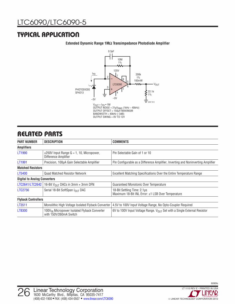
Extended Dynamic Range 1MΩ Transimpedance Photodiode Amplifier
6090 TA10
–
+
200k1%
100mW
22.1k1%
14
2
3LTC6090
PHOTODIODESFH213
125V
0.3pF
–3V–3V
10M1%
VOUT
VOUT = IPD • 1MOUTPUT NOISE = 21µVRMS (1kHz – 40kHz)OUTPUT OFFSET = 150µV MAXIMUMBANDWIDTH = 40kHz (–3dB)OUTPUT SWING = 0V TO 12V
IPD7
85
6