LTC4015 - Multichemistry Buck Battery Charger … · NTC NTCBIAS SYS SYSM5 OUTFET INTVCC DRVCC BG...
76
LTC4015 1 4015fb For more information www.linear.com/LTC4015 APPLICATIONS TYPICAL APPLICATION FEATURES DESCRIPTION Multichemistry Buck Battery Charger Controller with Digital Telemetry System 12V IN 2-Cell Li-Ion 8A Step-Down Battery Charger Controller Step-Down Charger Efficiency and Coulomb Counter Error vs Battery Charge Current L, LT, LTC, LTM, Linear Technology and the Linear logo are registered trademarks and PowerPath is a trademark of Linear Technology Corporation. All other trademarks are the property of their respective owners. n Multichemistry Li-Ion/Polymer, LiFePO 4 , or Lead- Acid Battery Charger with Termination n High Efficiency Synchronous Buck Battery Charger n Digital Telemetry System Monitors V BAT , I BAT , R BAT ,NTC Ratio (Battery Temperature), V IN , I IN , V SYSTEM , Die Temperature n Coulomb Counter and Integrated 14-Bit ADC n Wide Charging Input Voltage Range: 4.5V to 35V n Wide Battery Voltage Range: Up to 35V n Input Undervoltage Charge Current Limit Loop n Maximum Power Point Tracking n Optional I 2 C Serial Port Control n Input Current Limit Prioritizes System Load Output n Input and Output Ideal Diodes Provide Low Loss PowerPath™ Operation n Instant-On Operation with Discharged Battery n Portable Medical Instruments/Military Equipment n Industrial Handhelds/Lighting n Ruggedized Notebook/Tablet Computers The LTC ® 4015 is a complete synchronous buck controller/ charger with pin-selectable, chemistry specific charging and termination algorithms. The LTC4015 can charge Li-Ion/Polymer, LiFePO 4 , or lead- acid batteries. Battery charge voltage is pin selectable and I 2 C adjustable. Input current limit and charge current can be accurately programmed with sense resistors and can be individually adjusted via the I 2 C serial port. A digital telemetry system monitors all system power parameters. Safety timer and current termination algorithms are sup- ported for lithium chemistry batteries. The LTC4015 also includes automatic recharge, precharge (Li-Ion) and NTC thermistor protection. The LTC4015's I 2 C port allows user customization of charger algorithms, reading of charger status information, configuration of the maskable and programmable alerts, plus use and configuration of the Coulomb counter. Available in a 38-Lead 5mm × 7mm QFN package. CHARGE CURRENT (A) EFFICIENCY (%) COULOMB COUNTER ERROR (%) 4015 TA01b 100 90 95 80 85 70 75 60 55 65 50 0.5 0.0 –0.5 –1.0 –1.5 –2.0 0.1 10 1 EFFICIENCY QC ERROR LTC4015 V IN UVCLFB μCONTROLLER V IN 12V SMBALERT DV CC SCL SDA CELLS0 INTV CC CELLS1 CELLS2 CHEM0 CHEM1 RT V C CCREFP CCREFM EQ INFET CLP R SNSI CLN SYS SYSM5 4015 TA01a OUTFET SYS INTV CC DRV CC BOOST TG SW BG CSPM5 CSP CSN R NTCBIAS R SNSB BATSENS NTCBIAS NTC LEAD-ACID EQUALIZE CHARGE (PADDLE) GND SGND 2P5V CC MPPT R NTC 2-CELL Li-Ion BATTERY PACK T
-
Upload
trinhkhanh -
Category
Documents
-
view
233 -
download
0
Transcript of LTC4015 - Multichemistry Buck Battery Charger … · NTC NTCBIAS SYS SYSM5 OUTFET INTVCC DRVCC BG...

LTC4015
14015fb
For more information www.linear.com/LTC4015
APPLICATIONS
TYPICAL APPLICATION
FEATURES DESCRIPTION
Multichemistry Buck Battery Charger Controller with Digital Telemetry System
12VIN 2-Cell Li-Ion 8A Step-Down Battery Charger Controller Step-Down Charger Efficiency and Coulomb Counter Error vs
Battery Charge Current
L, LT, LTC, LTM, Linear Technology and the Linear logo are registered trademarks and PowerPath is a trademark of Linear Technology Corporation. All other trademarks are the property of their respective owners.
n Multichemistry Li-Ion/Polymer, LiFePO4, or Lead-Acid Battery Charger with Termination
n High Efficiency Synchronous Buck Battery Chargern Digital Telemetry System Monitors VBAT, IBAT,
RBAT,NTC Ratio (Battery Temperature), VIN, IIN, VSYSTEM, Die Temperature
n Coulomb Counter and Integrated 14-Bit ADCn Wide Charging Input Voltage Range: 4.5V to 35Vn Wide Battery Voltage Range: Up to 35Vn Input Undervoltage Charge Current Limit Loop n Maximum Power Point Trackingn Optional I2C Serial Port Controln Input Current Limit Prioritizes System Load Outputn Input and Output Ideal Diodes Provide Low Loss
PowerPath™ Operationn Instant-On Operation with Discharged Battery
n Portable Medical Instruments/Military Equipmentn Industrial Handhelds/Lightingn Ruggedized Notebook/Tablet Computers
The LTC®4015 is a complete synchronous buck controller/charger with pin-selectable, chemistry specific charging and termination algorithms.
The LTC4015 can charge Li-Ion/Polymer, LiFePO4, or lead-acid batteries. Battery charge voltage is pin selectable and I2C adjustable. Input current limit and charge current can be accurately programmed with sense resistors and can be individually adjusted via the I2C serial port. A digital telemetry system monitors all system power parameters.
Safety timer and current termination algorithms are sup-ported for lithium chemistry batteries. The LTC4015 also includes automatic recharge, precharge (Li-Ion) and NTC thermistor protection. The LTC4015's I2C port allows user customization of charger algorithms, reading of charger status information, configuration of the maskable and programmable alerts, plus use and configuration of the Coulomb counter.
Available in a 38-Lead 5mm × 7mm QFN package.
CHARGE CURRENT (A)
EFFI
CIEN
CY (%
)
COULOMB COUNTER ERROR (%
)
4015 TA01b
100
90
95
80
85
70
75
60
55
65
50
0.5
0.0
–0.5
–1.0
–1.5
–2.00.1 101
EFFICIENCYQC ERROR
LTC4015
VIN
UVCLFB
µCONTROLLER
VIN12V
SMBALERT
DVCC
SCL
SDA
CELLS0
INTVCC CELLS1
CELLS2
CHEM0
CHEM1
RT
VC
CCREFP
CCREFMEQ
INFET CLP
RSNSI
CLN SYS SYSM5
4015 TA01a
OUTFET
SYS
INTVCC
DRVCC
BOOST
TG
SW
BG
CSPM5
CSP
CSN
RNTCBIAS
RSNSB
BATSENS
NTCBIAS
NTC
LEAD-ACIDEQUALIZE
CHARGE
(PADDLE)GNDSGND 2P5VCCMPPT
RNTC
2-CELL Li-IonBATTERY
PACK
T

LTC4015
24015fb
For more information www.linear.com/LTC4015
TABLE OF CONTENTS Features ............................................................................................................................ 1Applications ....................................................................................................................... 1Typical Application ............................................................................................................... 1Description......................................................................................................................... 1Absolute Maximum Ratings ..................................................................................................... 3Order Information ................................................................................................................. 3Data Sheet Conventions ......................................................................................................... 3Pin Configuration ................................................................................................................. 3Electrical Characteristics ........................................................................................................ 4Typical Performance Characteristics .........................................................................................10Pin Functions .....................................................................................................................13Block Diagram ....................................................................................................................15I2C Timing Diagram .............................................................................................................16Operation..........................................................................................................................17Applications Information .......................................................................................................42Register Description ............................................................................................................49DETAILED Register Descriptions ..............................................................................................55Typical Applications .............................................................................................................72Package Description ............................................................................................................74Revision History .................................................................................................................75Typical Application ..............................................................................................................76Related Parts .....................................................................................................................76

LTC4015
34015fb
For more information www.linear.com/LTC4015
PIN CONFIGURATIONABSOLUTE MAXIMUM RATINGS(Notes 1, 5)
13 14 15 16
TOP VIEW
39GND
UHF PACKAGE38-LEAD (5mm × 7mm) PLASTIC QFN
17 18 19
38 37 36 35 34 33 32
24
25
26
27
28
29
30
31
8
7
6
5
4
3
2
1CELLS1
CELLS2
DVCC
SCL
SDA
SMBALERT
SGND
UVCLFB
VC
RT
NTC
NTCBIAS
SYS
SYSM5
OUTFET
INTVCC
DRVCC
BG
BOOST
TG
SW
2P5VCC
MPPT
CSP
CELL
S0
CHEM
1
CHEM
0
V IN
INFE
T
CLP
CLN
EQ
GND
CSPM
5
CCRE
FM
CCRE
FP
BATS
ENS
CSN
23
22
21
20
9
10
11
12
TJMAX = 125°C, θJA = 34°C/W (NOTE 1)
EXPOSED PAD (PIN 39) IS GND, MUST BE SOLDERED TO PCB GND
ORDER INFORMATIONLEAD FREE FINISH TAPE AND REEL PART MARKING* PACKAGE DESCRIPTION TEMPERATURE RANGE
LTC4015EUHF#PBF LTC4015EUHF#TRPBF 4015 38-Lead (5mm × 7mm) Plastic QFN –40°C to 125°C
LTC4015IUHF#PBF LTC4015IUHF#TRPBF 4015 38-Lead (5mm × 7mm) Plastic QFN –40°C to 125°C
Consult LTC Marketing for parts specified with wider operating temperature ranges. *The temperature grade is identified by a label on the shipping container.For more information on lead free part marking, go to: http://www.linear.com/leadfree/ For more information on tape and reel specifications, go to: http://www.linear.com/tapeandreel/. Some packages are available in 500 unit reels through designated sales channels with #TRMPBF suffix.
VIN, CSN ..................................................... –0.3V to 40VBOOST to SW.............................................. –0.3 to 5.5VBATSENS to CSN, CSP to CSN, CLP to CLN, CLP, CLN
to SYS ................................................................±0.3VDVCC, DRVCC ............................................. –0.3V to 5.5V CELLSO, CELLS1, CELLS2, CHEM0, CHEM1,
MPPT, EQ ..........................................–0.3V to INTVCCSDA, SCL, SMBALERT .............................. –0.3V to DVCCIUVCLFB (Note 4) ..................................................±200µAINTVCC Peak Output Current ................................100mAOperating Junction Temperature Range (Notes 2,3) ............................................. –40 to 125°CStorage Temperature Range ......................–65 to 150°C
DATA SHEET CONVENTIONS• VPINNAME and IPINNAME represents the voltage on a pin
or the pin current; VEQ = EQ Pin Voltage.
• Hexadecimal numbers are prefixed with 0x; 0x10 is a hexadecimal 10
• Register symbol names will be capitalized. Symbols within a register will be lower case;
en_meas_sys_valid_alert is bit 15 in register EN_LIMIT_ALERTS (0x0D)
• LiFePO4 is lithium iron phosphate, Li-Ion is used for both lithium-ion and lithium-ion polymer
• Lithium chemistries refers to LiFePO4 , lithium-ion, and lithium-ion polymer as a group.
• When a register name is used in square brackets, this means the 16 bit value associated with that register; For example [VBAT] is the 16 bit ADC measurement value of the per cell battery voltage.
http://www.linear.com/product/LTC4015#orderinfo

LTC4015
44015fb
For more information www.linear.com/LTC4015
ELECTRICAL CHARACTERISTICS
SYMBOL PARAMETER CONDITIONS MIN TYP MAX UNITS
VIN Input Supply Voltage Range Note 8 l 3.1 35 V
VBAT Battery Voltage Range Note 8 l 35 V
VCHARGE(TOL) Charge Voltage, Regulated Battery per Cell Tolerance, All Chemistries
Li-Ion ,4.2V per Cell; LiFePO4 3.6V per Cell; Lead-Acid 2.2V per Cell
l –1.25 1.25 %
Regulated Battery Charge Current Tolerance
Full-Scale VCSP–CSN/RSNSB l –2.0 2.0 %
VSYS SYS Pin Voltage Note 8 l 3.05 35 V
Quiescent Current IQ = IVIN + ICLP + ICLN + ISYS + ISW + ICSP + ICSN + IBATSENS
Battery Discharge Current (No Input Supply, Coulomb Counter Disabled)
Battery Only, Telemetry Inactive l 112 325 µA
Battery Only, Telemetry Active 1% Duty Cycle
l 140 364 µA
Battery Only, Telemetry Active Continuously
2.84 mA
IQ, Charging Charging, Switcher Suspended 3.00 mA
Charging, VBAT > VCHARGE (Note 7) 4.10 mA
IQ, Ship Mode Ship Mode (VIN = 0) l 5 40 µA
IVin VIN Pin Current Battery Only (No Input Supply) –200 200 nA
Charging <140 µA
ISYS SYS Pin Current Battery Only, Telemetry Off 100 µA
Battery Only, Telemetry On 2.75 mA
Charging, VBAT > VCHARGE (Note 7) 3.65 mA
VIN_DUVLO VIN to VBATSENS Differential Undervoltage (Must Be Satisfied for Charging)
Rising Threshold Hysteresis
l 140 200 100
250 mV mV
VIN_OVLO Input Overvoltage Lockout (Inhibits Charger)
Rising Threshold Hysteresis
l 37.7 38.6 1.4
39.5 V V
Input Undervoltage Current Limit
VUVCLFB UVCLFB Pin Regulation Range (8-Bit DAC)
VUVCLFB Maximum Code 0xFF VUVCLFB Minimum Code 0x00
l 1188 1200 4.6875
1212 mV mV
UVCLFB Pin Regulation DAC LSB 4.6875 mV
UVCLFB Pin Leakage Current VUVCLFB = 1.2V l –100 100 nA
Input Current Limit
Regulated Input Current Limit Tolerance Full-Scale VCLP–CLN/RSNSI l –2.0 2.0 %
ICL Input Current Limit Range ICL = (VCLP – CLN)/RSNSI 0.5 – 32 mV/RSNSI
Input Current Limit LSB Step Size 0.5 mV/RSNSI
CLP Input Current VCLP = 12V, VCLP–CLN = 32mV 45 µA
CLN Input Current VCLP = 12V, VCLP–CLN = 32mV –100 100 nA
CLP, CLN Common Mode Range Note 8 4 35 V
The l denotes the specifications which apply over the specified operating junction temperature range, otherwise specifications are at TA = 25°C. (Note 2), DVCC = 3.3V, UVCLFB = 1.5; CELLS1 = INTVCC; EQ, MPPT, CELLS0, CELLS2, CHEM0, CHEM1 = 0; RT = 95.3k; RCCREF = 301k, RNTCBIAS = RNTC = 10k; BATSENS = CSN = CSP; DRVCC = INTVCC; SYS = CLP = CLN. Conditions: Charging; VIN = 12V, SYS = 12V, BATSENS = 7.4V …..Battery Only; VIN = 0V, SYS = 8.4V, BATSENS = 8.4V

LTC4015
54015fb
For more information www.linear.com/LTC4015
SYMBOL PARAMETER CONDITIONS MIN TYP MAX UNITS
INTVCC Regulator (SYS is Supply Pin for This Regulator)
VINTVCC Internal Regulator Output Voltage No Load 5 V
Load Regulation IINTVCC = 50 mA 1.5 2.5 %
VINTVCC_CUVLO INTVCC Undervoltage Charger Lockout Rising Threshold Hysteresis
l 4.2 4.3 0.3
4.4 V V
VINTVCC_TUVLO INTVCC Undervoltage Telemetry System Lockout
Rising Threshold Hysteresis
l 2.75 2.85 0.12
2.95 V V
DRVCC INPUT (External Supply or Supplied by INTVCC)
VDRVCC DRVCC Supply Voltage 4.3 5.5 V
DRVCC Undervoltage Lockout Rising Threshold Hysteresis
l 4.1 4.2 0.3
4.3 V V
Battery Charger (All Chemistries)
ICHARGE Battery Charge Current Range, Battery Charge Current Resolution
VCSP > 2.6V (Note 10) 1 – 32 1
mV/RSNSB mV/RSNSB
Peak Low VCSP Charge Current VCSP < 2.4V 7.0 mV/RSNSB
IBATSENS + ICSP + ICSN Charger Suspended (Telemetry Active) VIN, VSYS = 12V, VBATSENS = 7.4V VIN, VSYS = 35V, VBATSENS = 34V (9 Cells)
110 200
µA µA
Lithium-Ion/Lithium Polymer Battery Charger
Lithium-Ion/Lithium Polymer Programmable, CHEM1, CHEM0 = [LL] (Note 9)
Li-Ion Charge Voltage Max DAC Setting Code 11111 (Note 11) 4.2 V/Cell
Li-Ion Charge Voltage Min DAC Setting Code 00000 (Note 11) 3.8125 V/Cell
Li-Ion Charge Voltage DAC LSB 12.5 mV
Li-Ion Recharge Voltage Percent of Charge Voltage 97.5 %
Charge C/x Termination Setting VCSP–CSN (I2C Termination Option) 3.2 mV
Lithium-Ion/Lithium Polymer Fixed 4.2, 4.1, 4.0 Charge Voltage, CHEM1, CHEM0 = [HH,LZ,ZL] (Note 9)
4.2V Fixed Li-Ion Charge Voltage CHEM1,0 = [H,H] (Note 11) 4.200 V/Cell
4.2V Fixed Li-Ion Recharge Voltage CHEM1,0 = [H,H] 4.095 V/Cell
4.1V Fixed Li-Ion Charge Voltage CHEM1,0 = [L,Z] (Note 11) 4.100 V/Cell
4.1V Fixed Li-Ion Recharge Voltage CHEM1,0 = [L,Z] 4.000 V/Cell
4.0V Fixed Li-Ion Charge Voltage CHEM1,0 = [Z,L] (Note 11) 4.000 V/Cell
4.0V Fixed Li-Ion Recharge Voltage CHEM1,0 = [Z,L] 3.900 V/Cell
Lithium-Ion/Lithium Polymer, CHEM1, CHEM0 = [LL, HH, LZ, ZL] (Note 9)
Low Battery Precharge Threshold Charge Voltage = 4.2V 2.85 V/Cell
Low Battery Precharge Hysteresis Charge Voltage = 4.2V 50 mV/Cell
Low Battery Precharge Current ICHARGE Set to 32 mV/RSNSB 3 mV/RSNSB
Max Charge Time 18.2 hrs
Charge Termination Timer (Default Termination) 4 hrs
ELECTRICAL CHARACTERISTICS The l denotes the specifications which apply over the specified operating junction temperature range, otherwise specifications are at TA = 25°C. (Note 2), DVCC = 3.3V, UVCLFB = 1.5; CELLS1 = INTVCC; EQ, MPPT, CELLS0, CELLS2, CHEM0, CHEM1 = 0; RT = 95.3k; RCCREF = 301k, RNTCBIAS = RNTC = 10k; BATSENS = CSN = CSP; DRVCC = INTVCC; SYS = CLP = CLN. Conditions: Charging; VIN = 12V, SYS = 12V, BATSENS = 7.4V …..Battery Only; VIN = 0V, SYS = 8.4V, BATSENS = 8.4V

LTC4015
64015fb
For more information www.linear.com/LTC4015
SYMBOL PARAMETER CONDITIONS MIN TYP MAX UNITS
LiFePO4 Battery ChargerLiFePO4, Programmable, CHEM1,CHEM0 = [LH] (Note 9)
LiFePO4 Charge Voltage Max DAC setting Code 11111 (Note 11) 3.8 V/Cell
LiFePO4 Charge Voltage Min DAC setting Code 00000 (Note 11) 3.4125 V/Cell
LiFePO4 Charge Voltage DAC LSB 12.5 mV
LiFePO4 Recharge Voltage POR Value I2C Programmable 3.35 V/Cell
VLiFePO4-C/x Charge Termination C/x Threshold VCSP-CSN (I2C Programmable) 3.2 mV
LiFePO4 Fixed Standard Charge, Fixed Fast Charge, CHEM1, CHEM0 = [ZH,HZ] (Note 9)LiFePO4 Fixed Fast Charge Absorb Voltage CHEM1, CHEM0 = [HZ] Only (Note 11) 3.8 V/Cell
LiFePO4 Charge Voltage CHEM1, CHEM0 = [ZH,HZ] (Note 11) 3.6 V/Cell
LiFePO4 Recharge Voltage CHEM1, CHEM0 = [ZH,HZ] (Note 11) 3.35 V/Cell
LiFePO4, CHEM1, CHEM0 = [LH,HZ,ZH] (Note 9)Max Charge Time 18.2 hrs
VLiFePO4-T(CV) Charge Termination Time 1 hrs
Lead-Acid Battery ChargerLead-Acid Fixed, CHEM1, CHEM0 = [ZZ] (Note 9)VLead_Acid_Vcharge Lead-Acid VCHARGE, Equalization
Lead-Acid VCHARGE, Absorption Lead-Acid VCHARGE, CV Lead-Acid Temperature Compensation
(Note 11) (Note 11) (Note 11)
2.6 2.4 2.2
–3.65
V/Cell V/Cell V/Cell
mV/Cell/°C
Lead-Acid Programmable, CHEM1, CHEM0 = [HL] (Note 9)VLead_Acid_Vcharge Lead-Acid VCHARGE DAC Maximum
Lead-Acid VCHARGE DAC Minimum Lead-Acid VCHARGE DAC Resolution Lead-Acid Temperature Comp
Code 111111 (Note 11) Code 000000 (Note 11) Temperature Comp Enabled
2.6 2.0 9.5
–3.65
V/Cell V/Cell
mV mV/Cell/°C
Thermistor (NTC) BIASVNTCBIAS Applied NTC Bias Voltage Internally Switched to 1.2V 1.2 V
INTC NTC Leakage Current –50 50 nA
SYSM5, CSPM5 Regulators–5VVINM5 VSYS – VSYSM5, VCSP – VCSPM5 No Load 4.8 V
Power Path/Ideal Diode ControllersVFTO Forward Turn-On Voltage 50 mV
VFR Forward Regulation 15 mV
VRTO Reverse Turn-Off –30 mV
tIF(ON) INFET Turn-On Time INFET – VIN > 3V, CINFET = 3.3nF 550 µs
tIF(OFF) INFET Turn-Off Time INFET – VIN < 1V, CINFET = 3.3nF 2 µs
tOF(ON) OUTFET Turn-On Time VBAT – OUTFET > 3V, COUTFET = 3.3nF 2.3 µs
tOF(OFF) OUTFET Turn-Off Time VBAT – OUTFET < 1V, COUTFET = 3.3nF 1.9 µs
Inductor Current Regulation
ILIM Cycle by Cycle Max Charge Current Note 5 l 47 52 57 mV/RSNSB
IREV Reverse Inductor Current l 3.8 7.0 10 mV/RSNSB
ELECTRICAL CHARACTERISTICS The l denotes the specifications which apply over the specified operating junction temperature range, otherwise specifications are at TA = 25°C. (Note 2), DVCC = 3.3V, UVCLFB = 1.5; CELLS1 = INTVCC; EQ, MPPT, CELLS0, CELLS2, CHEM0, CHEM1 = 0; RT = 95.3k; RCCREF = 301k, RNTCBIAS = RNTC = 10k; BATSENS = CSN = CSP; DRVCC = INTVCC; SYS = CLP = CLN. Conditions: Charging; VIN = 12V, SYS = 12V, BATSENS = 7.4V …..Battery Only; VIN = 0V, SYS = 8.4V, BATSENS = 8.4V

LTC4015
74015fb
For more information www.linear.com/LTC4015
SYMBOL PARAMETER CONDITIONS MIN TYP MAX UNITS
Oscillator
fOSC Switching Frequency RT = 95.3k l 475 500 525 kHz
fMAX Maximum Programmable Frequency RT = 47.5k 1 MHz
fMIN Minimum Programmable Frequency RT = 237k 200 kHz
Gate Drivers
RUP-TG TG Pull-Up On-Resistance 2.0 Ω
RDOWN-TG TG Pull-Down On-Resistance 0.5 Ω
RUP-BG BG Pull-Up On-Resistance 2.0 Ω
RDOWN-BG TG Pull-Down On-Resistance 0.5 Ω
tR-TG TG 10% to 90% Rise Time CLOAD = 3.3nF 20 ns
tF-TG TG 90% to 10% Fall Time CLOAD = 3.3nF 10 ns
tR-BG BG 10% to 90% Rise Time CLOAD = 3.3nF 20 ns
tF-BG BG 90% to 10% Fall Time CLOAD = 3.3nF 10 ns
tNO Non-Overlap Time 60 ns
tON(MIN) Minimum On-Time 140 ns
DCMAX Maximum Duty Cycle 98.4 %
VC Error Amplifier
gm Transconductance to VC pin gm (VCSP–CSM) (Constant-Current) gm (VBATSENS) (Constant-Voltage Lithium) gm (VBATSENS) (Constant-Voltage LA) gm (VUVCLFB) (Input Voltage Regulation) gm (VCLP–CLM) (Input Current Limiting)
2 Cell; (gm = 1.06 –3 • 2/(7 • Cell Count) 6 Cell; (gm = 1.06 –3 • 3/(7 • Cell Count)
4.10 0.15 0.08 1.06 4.10
mmho mmho mmho mmho mmho
Telemetry A/D Measurement Subsystem, Battery Only Mode
VERR Measurement Error (Note 6) VIN = 1V VIN = 35V
±100 ±1.5
mV %
VSYS = 2.5V VSYS = 35V
±100 ±1.5
mV %
VBAT = 1.75V, 1 Cell Li-Ion VBAT = 35V, 9 Cell Li-Ion
±50 ±1.5
mV %
VCLP–CLN = 0mV VCLP–CLN = 32mV
±200 ±2.5
µV %
VCSP–CSN = 0mV VCSP–CSN = 32mV
±200 ±2.5
µV %
NTC/NTCBIAS = 50%, 75% NTC/NTCBIAS = 5%
±2 ±3.5
% %
ELECTRICAL CHARACTERISTICS The l denotes the specifications which apply over the specified operating junction temperature range, otherwise specifications are at TA = 25°C. (Note 2), DVCC = 3.3V, UVCLFB = 1.5; CELLS1 = INTVCC; EQ, MPPT, CELLS0, CELLS2, CHEM0, CHEM1 = 0; RT = 95.3k; RCCREF = 301k, RNTCBIAS = RNTC = 10k; BATSENS = CSN = CSP; DRVCC = INTVCC; SYS = CLP = CLN. Conditions: Charging; VIN = 12V, SYS = 12V, BATSENS = 7.4V …..Battery Only; VIN = 0V, SYS = 8.4V, BATSENS = 8.4V

LTC4015
84015fb
For more information www.linear.com/LTC4015
SYMBOL PARAMETER CONDITIONS MIN TYP MAX UNITS
Coulomb Counter
VSENSE Sense Voltage Differential Input Range VCSP–CSN ±50 mV
qLSB Charge Measurement Resolution Prescaler M = 512 (Default) 0.017 mVhr
TCE Total Charge Error 10mV ≤ |VSENSE| ≤ 50mV ±1.5 %
10mV ≤ |VSENSE| ≤ 50mV l ±2.5 %
VSENSE = 1mV <1.0 %
IQC_CSP IQ– Coulomb Counter VSENSE = 30mV, Battery Only 78 μA
CELLS0, CELLS1, CELLS2, CHEM0, CHEM1 Programming Input Pins (Note 9)
VIHPP Input High Threshold INTVCC – VPIN l 0.3 V
VILPP Input Low Threshold VPIN l 0.3 V
RIZPP Input High-Z Test Resistance Internal 50k/50k Resistor Divider Applied to Inputs During Chemistry/Cell Read
25 kΩ
MPPT, EQ Input Pins
MPPT, EQ Input High Threshold l 1.1 V
MPPT, EQ Input Low Threshold l 0.2 V
MPPT, EQ Pin Leakage Current VEQ, VMPPT = 5V 0 1 µA
SMBALERT Pin Characteristics
ISMBALERT SMBALERT Pin Leakage Current VSMBALERT = 5V 0 1 µA
VSMBALERT SMBALERT Pin Output Low Voltage ISMBALERT = 1mA 65 100 mV
I2C Port, SDA, SCL
DVCC I2C Logic Reference Level 1.6 5.5 V
IDVCCQ DVCC Current SCL/SDA = 0kHz 0 µA
ADDRESS I2C Address 1101_000[R/W]b
VIHI2C Input High Threshold 70 % DVCC
VILI2C Input Low Threshold 30 % DVCC
IIHI2C Input Leakage High –1 1 µA
IILI2C Input Leakage Low –1 1 µA
VOLI2C Digital Output Low (SDA) ISDA = 3mA 0.4 V
FSCL SCL Clock Frequency 400 kHz
tLOW LOW Period of SCL Clock 1.3 µS
tHIGH HIGH Period of SCL Clock 0.6 µS
tBUF Bus Free Time Between Start and Stop Conditions
1.3 µs
tHD(STA) Hold Time, After (Repeated) Start Condition
0.6 µs
tSU(STA) Setup Time After a Repeated Start Condition
0.6 µs
tSU(STO) Stop Condition Set-Up Time 0.6 µs
ELECTRICAL CHARACTERISTICS The l denotes the specifications which apply over the specified operating junction temperature range, otherwise specifications are at TA = 25°C. (Note 2), DVCC = 3.3V, UVCLFB = 1.5; CELLS1 = INTVCC; EQ, MPPT, CELLS0, CELLS2, CHEM0, CHEM1 = 0; RT = 95.3k; RCCREF = 301k, RNTCBIAS = RNTC = 10k; BATSENS = CSN = CSP; DRVCC = INTVCC; SYS = CLP = CLN. Conditions: Charging; VIN = 12V, SYS = 12V, BATSENS = 7.4V …..Battery Only; VIN = 0V, SYS = 8.4V, BATSENS = 8.4V

LTC4015
94015fb
For more information www.linear.com/LTC4015
SYMBOL PARAMETER CONDITIONS MIN TYP MAX UNITS
tHD(DAT(OUT)) Output Data Hold Time 0 900 ns
tHD)DAT(IN)) Input Data Hold Time 0 ns
tSU(DAT) Data Set-Up Time 100 ns
tSP Input Spike Suppression Pulse Width 50 ns
Note 1: Stresses beyond those listed under Absolute Maximum Ratings may cause permanent damage to the device. Exposure to any Absolute Maximum Rating condition for extended periods may affect device reliability and lifetime.Note 2: The LTC4015 is tested under pulsed load conditions such that TJ ≈ TA. The LTC4015E is guaranteed to meet specifications from 0°C to 85°C junction temperature. Specifications over the –40°C to 125°C operating junction temperature range are assured by design, characterization and correlation with statistical process controls. The LTC4015I is guaranteed over the –40°C to 125°C operating junction temperature range. Note that the maximum ambient temperature consistent with these specifications is determined by specific operating conditions in conjunction with board layout, the rated package thermal impedance and other environmental factors. The junction temperature (TJ, in °C) is calculated from the ambient temperature (TA, in °C) and power dissipation (PD, in Watts) according to the formula:
TJ = TA + (PD • θJA) where θJA = 34°C/W for the UHF package.Note 3: The LTC4015 includes overtemperature protection that is intended to protect the device during momentary overload conditions. The maximum rated junction temperature will be exceeded when this protection is active. Continuous operation above the specified absolute maximum operating junction temperature may impair device reliability or permanently damage the device.Note 4: UVCLFB is internally clamped above the maximum UVCLFB regulation point (2.5V at 200µA nominally). Maximum input current must be limited to 200µA when this clamp is reached.
Note 5: The current limit features of this part are intended to protect the IC from short term or intermittent fault conditions. Continuous operation above the maximum specified pin current may result in device degradation or failure.Note 6: Measurement error is the magnitude of the difference between the actual measured value and the ideal value. Error for VCLP-CLN and VCSP-CSN is expressed in μV, a conversion to an equivalent current may be made by dividing by the sense resistors, RSNSI and RSNSB, respectively.Note 7: VCHARGE is the battery charge voltage (or CV, constant-voltage) target. VBAT is the battery voltage. Dynamic supply current is higher due to the gate charge being delivered at the switching frequency. See the Applications Information section.Note 8: VIN, or VBAT for battery only operation, may be connected to any suitable DC power source from 2.8V to 35V such that the voltage at VSYS is high enough to allow INTVCC to support the desired mode of operation. In order for the telemetry system to operate, INTVCC must exceed the telemetry undervoltage lockout (VINTVCC_TUVLO). In order for the battery charger to operate, INTVCC must exceed the charger undervoltage lockout (VINTVCC_CUVLO). Allowing for 0.3V of drop from VIN to INTVCC, these modes require a minimum input voltage of 3.1V and 4.35V, respectively. Additionally the VIN to VBATSENS (VIN_DULVO) differential must also be satisfied for charging.Note 9: Chemistry selection is made using the CHEM1 and CHEM0 pins. These are three-state pins used by the LTC4015 to select of one of nine chemistry specific charging algorithms. These pins should be hard wired to GND(L), INTVCC(H), or left open (Z > 1000kΩ).Note 10: ICHARGE is the battery charge current (or CC, constant-current) target. ICHG is the charge current when charging.Note 11: Charge voltage tolerance is VCHARGE(TOL) which is specified at the beginning of the electrical table. The LTC4015 is not a substitute for pack protection! The 4015 does not monitor or balance individual cells – the full stack voltage is divided by number of cells for simplicity only.
ELECTRICAL CHARACTERISTICS The l denotes the specifications which apply over the specified operating junction temperature range, otherwise specifications are at TA = 25°C. (Note 2), DVCC = 3.3V, UVCLFB = 1.5; CELLS1 = INTVCC; EQ, MPPT, CELLS0, CELLS2, CHEM0, CHEM1 = 0; RT = 95.3k; RCCREF = 301k, RNTCBIAS = RNTC = 10k; BATSENS = CSN = CSP; DRVCC = INTVCC; SYS = CLP = CLN. Conditions: Charging; VIN = 12V, SYS = 12V, BATSENS = 7.4V …..Battery Only; VIN = 0V, SYS = 8.4V, BATSENS = 8.4V

LTC4015
104015fb
For more information www.linear.com/LTC4015
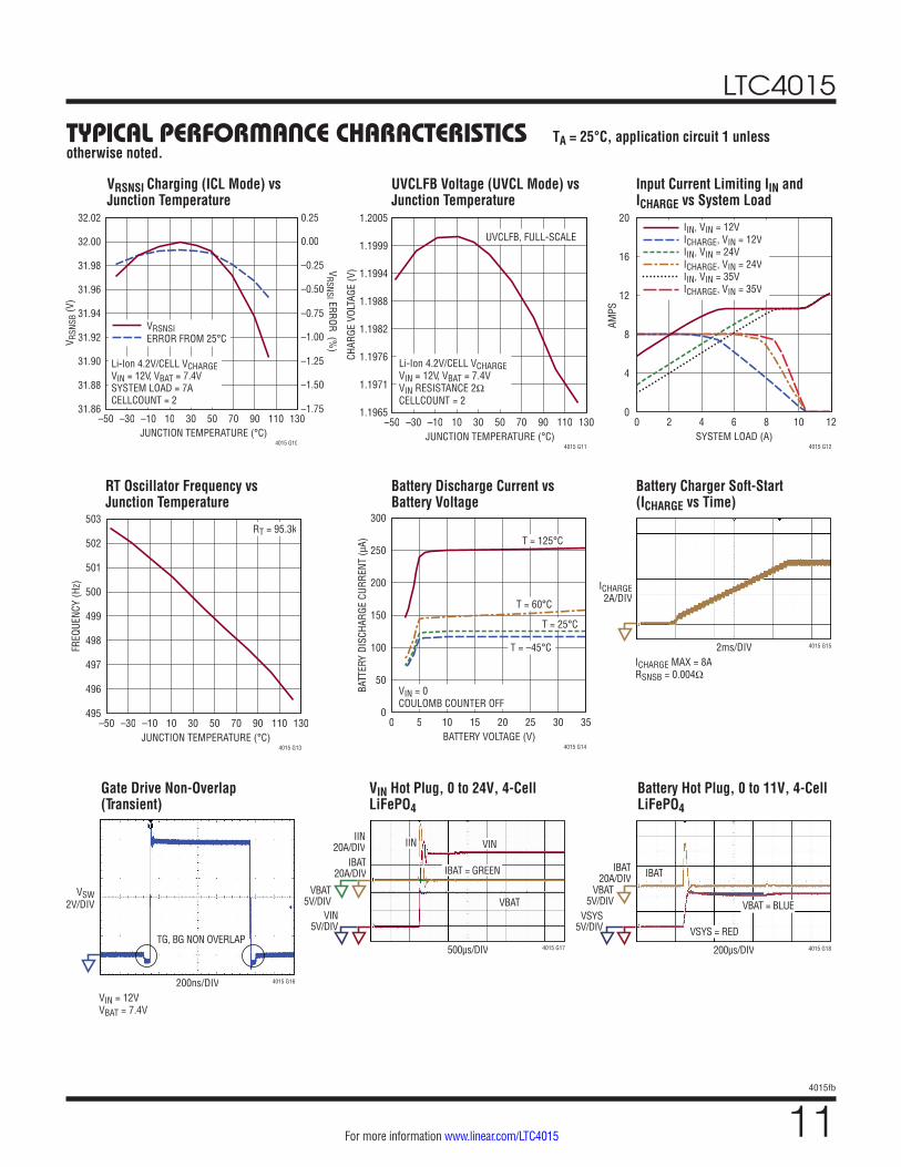
TYPICAL PERFORMANCE CHARACTERISTICS
VIN (Resistive), MPPT Enabled Charger On/Off Li-Ion Charging Efficiency vs VIN
Lead-Acid Charging Efficiency vs ICHARGE
LiFePO4 Charging Efficiency vs ICHARGE
Charge Voltage (CV Mode) vs Junction Temperature
VRSNSB Current (CC Mode) vs Junction Temperature
Lead-Acid Charging ProfileVoltage, Current vs Time
Li-Ion Charging ProfileVoltage, Current vs Time
LiFePO4 Charging ProfileVoltage, Current vs Time
TA = 25°C, application circuit 1 unless otherwise noted.
TIME (MINUTES)0 50 100 150 200 250
11.0
11.5
12.0
12.5
13.0
13.5
14.0
14.5
15.0
0
0.5
1.0
1.5
2.0
2.5
3.0
3.5
BATT
ERY
VOLT
AGE
(V) BATTERY CURRENT (A)
4015 G01
CHARGE VOLTAGECHARGE CURRENT
VABSORB = 2.4V/CELLVCHARGE = 2.2V/CELL
CELLCOUNT = 6RSNSI = 0.007ΩRSNSB = 0.010Ω
TIME (MINUTES)0 15 30 45 60 75 90 105 120 135
7.2
7.4
7.6
7.8
8.0
8.2
8.4
8.6
0
1
2
3
4
5
6
7
8
BATT
ERY
VOLT
AGE
(V) BATTERY CURRENT (A)
4015 G02
CHARGE VOLTAGECHARGE CURRENT
VCHARGE = 4.2V/CELL
CELLCOUNT = 2
TIME (MINUTES)0 15 30 45 60 75 90 105 120 135
11.0
11.5
12.0
12.5
13.0
13.5
14.0
14.5
15.0
0
1
2
3
4
5
6
7
8
BATT
ERY
VOLT
AGE
(V) BATTERY CURRENT (A)
4015 G03
CHARGE VOLTAGECHARGE CURRENT
VCHARGE = 3.6V/CELLCELLCOUNT = 4
VIN, CHARGER OFF (V)10 15 20 25 30 35
0
5
10
15
20
25
30
V IN
CHAR
GER
ON (V
)
4015 G04
VIN, MPPT ENABLEDVIN/2, CHARGER OFFVBAT + 1V
VIN RESISTANCE 4.5Ω
VCHARGE = 4.2V/CELLVBAT HELD AT 6.6V
VIN (V)10 15 20 25 30
80
82
84
86
88
90
92
94
96
EFFI
CIEN
CY (%
)
4015 G05
ICHARGE = 0.75AICHARGE = 4AICHARGE = 8A
VBAT HELD AT 7.4VCELLCOUNT = 2
ICHARGE (A)0 1 2 3 4 5 6 87
70
75
80
85
90
95
100
EFFI
CIEN
CY (%
)
4015 G06
ICHARGE
VIN = 24VVBAT HELD AT 12.2VCELLCOUNT = 6
ICHARGE (A)0 1 2 3 4 5 6 7 8
84
86
88
90
92
94
96
98
EFFI
CIEN
CY (%
)
4015 G07
ICHARGE
VIN = 30VVBAT HELD AT 23.5VCELLCOUNT = 7
JUNCTION TEMPERATURE (°C)–50 –30 –10 10 30 50 70 90 110 130
8.370
8.375
8.380
8.385
8.390
8.395
8.400
8.405
CHAR
GE V
OLTA
GE (V
)
4015 G08
ICHARGE = 0ICHARGE = 100mA
Li-Ion 4.2V/CELL CHARGE VOLTAGEVIN = 12VCELLCOUNT = 2
JUNCTION TEMPERATURE (°C)–50 –30 –10 10 30 50 70 90 110 130
31.86
31.88
31.90
31.92
31.94
31.96
31.98
32.00
32.02
–1.75
–1.50
–1.25
–1.00
–0.75
–0.50
–0.25
0.00
0.25
V RSN
SB (V
)
VRSNSB ERROR (%
)
4015 G09
Li-Ion 4.2V/CELL CHARGE VOLTAGEVIN = 12.V, VBAT = 8VCELLCOUNT = 2
FULL-SCALE VRSNSBERROR FROM 25°C
LTC4015
114015fb
For more information www.linear.com/LTC4015
TYPICAL PERFORMANCE CHARACTERISTICS
RT Oscillator Frequency vs Junction Temperature
Battery Discharge Current vs Battery Voltage
Battery Charger Soft-Start (ICHARGE vs Time)
Gate Drive Non-Overlap (Transient)
VIN Hot Plug, 0 to 24V, 4-Cell LiFePO4
Battery Hot Plug, 0 to 11V, 4-Cell LiFePO4
VRSNSI Charging (ICL Mode) vs Junction Temperature
UVCLFB Voltage (UVCL Mode) vs Junction Temperature
Input Current Limiting IIN and ICHARGE vs System Load
TA = 25°C, application circuit 1 unless otherwise noted.
JUNCTION TEMPERATURE (°C)–50 –30 –10 10 30 50 70 90 110 130
1.1965
1.1971
1.1976
1.1982
1.1988
1.1994
1.1999
1.2005
CHAR
GE V
OLTA
GE (V
)
4015 G11
UVCLFB, FULL-SCALE
Li-Ion 4.2V/CELL VCHARGEVIN = 12V, VBAT = 7.4VVIN RESISTANCE 2ΩCELLCOUNT = 2
SYSTEM LOAD (A)0 2 4 6 8 10 12
0
4
8
12
16
20
AMPS
4015 G12
IIN, VIN = 12VICHARGE, VIN = 12VIIN, VIN = 24VICHARGE, VIN = 24VIIN, VIN = 35VICHARGE, VIN = 35V
JUNCTION TEMPERATURE (°C)–50 –30 –10 10 30 50 70 90 110 130
495
496
497
498
499
500
501
502
503
FREQ
UENC
Y (H
z)
4015 G13
RT = 95.3k
JUNCTION TEMPERATURE (°C)–50 –30 –10 10 30 50 70 90 110 130
31.86
31.88
31.90
31.92
31.94
31.96
31.98
32.00
32.02
–1.75
–1.00
–1.25
–1.50
–0.75
–0.50
–0.25
0.00
0.25
V RSN
SB (V
)
VRSNSI ERROR (%
)
4015 G10
VRSNSIERROR FROM 25°C
Li-Ion 4.2V/CELL VCHARGEVIN = 12V, VBAT = 7.4VSYSTEM LOAD = 7ACELLCOUNT = 2
BATTERY VOLTAGE (V)0 5 10 15 20 25 30 35
0
50
100
150
200
250
300
BATT
ERY
DISC
HARG
E CU
RREN
T (µ
A)
4015 G14
T = –45°C
T = 25°C
T = 60°C
T = 125°C
VIN = 0COULOMB COUNTER OFF
ICHARGE MAX = 8ARSNSB = 0.004Ω
2ms/DIV 4015 G15
ICHARGE2A/DIV
VIN = 12VVBAT = 7.4V
VSW2V/DIV
200ns/DIV 4015 G16
TG, BG NON OVERLAP4015 G17
IIN VIN
VBAT
IIN20A/DIV
IBAT20A/DIV
VIN5V/DIV
VBAT5V/DIV
500µs/DIV
IBAT = GREEN
4015 G18
IBATIBAT20A/DIV
VBAT5V/DIV
VSYS5V/DIV
VBAT = BLUE
VSYS = RED
200µs/DIV

LTC4015
124015fb
For more information www.linear.com/LTC4015
TYPICAL PERFORMANCE CHARACTERISTICS
Coulomb Counter Accuracy vs VCSP–CSN
Start-Up from 24V VIN Hot Plug, ICHARGE = 8A (RSNSB = 0.004Ω)
Ship Mode Battery Discharge Current vs Battery Voltage
MPPT Algorithm Using UVCL DAC Sweep to Find MPP
VCSP – VCSN (mV)
ERRO
R (%
)
4015 G24
0.5%
0.0%
–0.5%
–1.0%
–1.5%
–2.0%
–2.5%
3.0%
3.5%0 15 20 25 30 35105
QC ERROR
BATTERY VOLTAGE (V)0 5 10 15 20 25 30 35
0
5
10
15
20
25
30
35
BATT
ERY
DISC
HARG
E CU
RREN
T (µ
A)
4015 G20
T = 125°CT = 60°CT = 25°CT = –45°C
VIN SOURCE IMPEDANCE = 4.4Ω
4015 G21
MAXIMUM ICHARGE FOUNDDURING UVCL DAC SWEEP
VBAT
VIN , AT MAX ICHARGEFOUND DURING UVCLDAC SWEEP
VIN, NOLOAD = 25V
UVCL DACSWEEP
VIN5V/DIV
VBAT5V/DIV
ICHARGE2A/DIV
400ms/DIV
4015 G19
IBAT
IIN
VBAT
VINVIN5V/DIV
VBAT5V/DIV
IIN5A/DIV
IBAT5A/DIV
200µs/DIV

LTC4015
134015fb
For more information www.linear.com/LTC4015
PIN FUNCTIONSCELLS1 (Pin 1): Number of Cells Select Pin. Three-state pin used in combination with CELLS0 and CELLS2 to set the total number of battery cells.
CELLS2 (Pin 2): Number of Cells Select Pin. Three-state pin used in combination with CELLS0 and CELLS1 to set the total number of battery cells.
DVCC (Pin 3): Logic Supply for the I2C Serial Port. DVCC sets the reference level of the SDA and SCL pins for I2C compliance. It must be connected to the same power supply used to power the I2C pull up resistors. If the I2C port is unused connect this pin to INTVCC, do not float.
SCL (Pin 4): Clock Input for the I2C Serial Port. The I2C input levels are scaled with respect to DVCC for I2C compliance. If the I2C port is unused connect this pin to INTVCC, do not float.
SDA (Pin 5): Data Input/Output for the I2C serial port. The I2C input levels are scaled with respect to DVCC for I2C compliance. If the I2C port is unused connect this pin to INTVCC, do not float.
SMBALERT (Pin 6): Open-Drain Interrupt Request. Pulls low when something important needs to be reported back to the system.
SGND (Pin 7): Signal Ground. All small signal components and compensation should connect to this ground, which should be connected to PGND at a single point.
UVCLFB (Pin 8): Undervoltage Current Limit Feedback Pin. UVCLFB can be used to reduce charge current when the VIN pin reaches a level programmed by the user sup-plied resistor divider. This feature can be used for power sources with higher source impedance such as a solar panel. Maximum charge current is tapered off when this pin is below 1.2V, at 1.15V the charge current is zero. UVCLFB is internally clamped to about 2.5V with 200µA in this pin. Limit the current into this pin to 200µA at maximum VIN using the thevenin resistance of the input divider. If the input undervoltage current limit feature is not desired, connect UVCLFB to 2P5VCC through a 10k resistor or to VIN through an appropriately sized resistor.
VC (Pin 9): Current Control Threshold and Error Amplifier Compensation Point. The current comparator threshold increases with this control voltage. The voltage normally ranges from 900mV to 2.4V.
RT (Pin 10): Connect a resistor from RT to GND to set frequency of the switching power supply.
NTC (Pin 11): Thermistor Input. The NTC pin connects to a negative temperature coefficient thermistor (Type_2) to monitor the temperature of the battery. The voltage on this pin is digitized by the analog to digital converter and is available via the I2C port. The thermistor value is also used to qualify battery charging. Connect a low drift bias resistor from NTCBIAS to NTC and a thermistor from NTC to ground. If NTC functions are unwanted, use a resistor equal in value to RNTCBIAS instead of a thermistor.
NTCBIAS (Pin 12): NTC Thermistor Bias Output. Connect a bias resistor between NTCBIAS and NTC, and a thermis-tor between NTC and GND. The bias resistor should be equal in value to the nominal value of the thermistor. The LTC4015 applies 1.2V to this pin during NTC measurement.
EQ (Pin 13): Equalize. Apply a logic signal between 1.5V and INTVCC (5V) to this pin to allow the 4015 to trigger lead-acid equalize mode. GND this pin if unused, do not float.
GND (Pin 14, Exposed Pad Pin 39): Ground. The exposed pad should be connected by multiple vias directly under the LTC4015 to a continuous ground plane on the second layer of the printed circuit board.
CSPM5 (Pin 15): Internal Supply Pin. The VCSPM5 pin regulates at the higher of ground or approximately VCSP – 5V. A low impedance multilayer ceramic capacitor should be connected from VCSP to VCSPM5.
CCREFM (Pin 16): Coulomb Counter Reference Resis-tor Pin. Leakage on this pin will affect Coulomb counter accuracy. Connect a 301k, 0.1%, 25ppm resistor from CCREFM to CCREP.
CCREFP (Pin 17): Coulomb Counter Reference Resis-tor Pin. CCREFP in conjunction with CCREFM provide a reference for the Coulomb counter to make an accurate measure of charge into and out of the battery. CCREFP is connected internally to CSP with 50Ω. Connect a 301k, 0.1%, 25ppm resistor from CCREFP to CCREM.

LTC4015
144015fb
For more information www.linear.com/LTC4015
PIN FUNCTIONSBATSENS (Pin 18): Battery Voltage Sense Input. For proper operation, this pin must be connected physically close to the positive input terminal of the battery.
CSN (Pin 19): Connection Point for the Negative Terminal of the Charge Current Sense Resistor.
CSP (Pin 20): Connection Point for the Positive Terminal of the Charge Current Sense Resistor.
MPPT (Pin 21): MPPT Enable Pin. Apply a logic signal between 1.5V and INTVCC (5V) to this pin to allow the 4015 to enter MPPT mode. MPPT mode can also be entered via the I2C port. GND this pin if unused, do not float.
2P5VCC (Pin 22): Bypass Pin for the Internal 2.5V Regu-lator. This regulator provides power to the internal logic circuitry. Bypass 2P5VCC with a 2.2μF multilayer ceramic capacitor to GND.
SW (Pin 23): Switch Node. SW pin swings from a diode drop below ground up to VSYS.
TG (Pin 24): Top Gate Drive. Drives the top N-channel MOSFET with a voltage swing equal to DRVCC superim-posed on the switch node voltage VSW.
BOOST (Pin 25): Boosted Floating Top Gate Drive Supply. The BOOST pin swings from a diode voltage below DRVCC up to VSYS + DRVCC.
BG (Pin 26): Bottom Gate Drive. Drives the bottom N-channel MOSFET between DRVCC and ground.
DRVCC (Pin 27): External Supply for Gate Driver. Do not exceed 5.5V on this pin. If DRVCC is not connected to INTVCC, INTVCC must be greater than 3V before DRVCC is applied. If not connected to INTVCC bypass this pin to ground with a low ESR ceramic capacitor.
INTVCC (Pin 28): Internal 5V Regulator Output. The control circuits and optionally the gate drivers are powered from this pin. Bypass this pin to ground with a minimum 4.7µF low ESR tantalum or ceramic capacitor.
OUTFET (Pin 29): Output Ideal Diode Gate Control Pin for External P-channel MOSFET.
SYSM5 (Pin 30): Internal Supply Pin. The VSYSM5 pin regulates at the higher of ground or approximately VSYS – 5V. A low impedance multilayer ceramic capacitor should be connected from VSYS to VSYSM5.
SYS (Pin 31): System Input Voltage. Primary power input to the 4015. This pin powers the internal INTVCC LDO. SYS is the max of VBAT or VIN. VSYS should be bypassed with a low impedance multilayer ceramic capacitor, along with large bulk capacitors.
CLN (Pin 32): Connection Point for the Negative Terminal of the Input Current Sense Resistor.
CLP (Pin 33): Connection Point for the Positive Terminal of the Input Current Sense Resistor.
INFET (Pin 34): Input Ideal Diode Gate Control Pin for External N-channel MOSFET.
VIN (Pin 35): Supply Voltage for the PowerPath Step-down Switching Charger. VIN may be connected to any suitable DC power source from 2.8V to 35V such that the voltage at VSYS is high enough to allow INTVCC to support the desired mode of operation. In order for the telemetry system to operate INTVCC must exceed the telemetry undervoltage lockout. VIN should be bypassed with a low impedance multilayer ceramic capacitor.
CHEM0 (Pin 36): Chemistry Select Pin. Three-state pin used in combination with CHEM1 to set the battery chemistry and charge algorithm.
CHEM1 (Pin 37): Chemistry Select Pin. Three-state pin used in combination with CHEM0 to set the battery chemistry and charge algorithm.
CELLS0 (Pin 38): Number of Cells Select Pin. Three-state pin used in combination with CELLS1 and CELLS2 to set the total number of battery cells.

LTC4015
154015fb
For more information www.linear.com/LTC4015
BLOCK DIAGRAM
CLP
15mV D/A6-BIT
1.2V FULL-SCALE
D/A5b LITHIUM CHEMISTRIES6b LEAD-ACID
37.5
VIN INFET SYSM5 SYS OUTFET
CLN
BATSENS
UVCLFB
VC
DVCC
SCL
SDA
SMBALERT
CHEM1
CHEM0
CELLS2
CELLS1
CELLS0
MPPT
EQ
+–
–
+
D/A5-BIT
1.2V FULL-SCALE
–
+
–+
–
+
–
+
–
+
D/A8-BIT
1.2V FULL-SCALE
RT
LOGIC
±1.8V RANGE, SIGNED 16BITS LSB(1 COUNT) = 3.6V/65535 = 54.9325µV
STEP-DOWNSWITCHING
CONTROLLER
I2C
–5V LDO
COULOMBCOUNTER
OSCILLATOR
–
+CCREFP
CSP
CSPM5
CCREFM
CSN
BOOST
TG
SW
DRVCC
BG
VSYS
NTC
GND4015 BD
GND
GND (PADDLE)GND
–5V LDO
A/D
VBATSENS /[CELLCOUNT • (7/2)] Li CHEMISTRIESVBATSENS /[CELLCOUNT • (7/3)] LEAD-ACIDVIN/30
VSYS/30
IBAT (37.5 • (VCSP – VCSN))
IIN (37.5 • (VCLP – VCLN))
T_DIE
INTVCC
2P5VCC
NTCBIAS
1.2V
INTVCCLDO
2.5V LDO
15mV
+–
37.5 37.5
IIN
IBAT
NTC
T_DIE
VSYS
VIN
VBAT
11
12
22
28
26
27
23
24
25
19
16
17
20
15
2931303435
33
32
18
8
9
10
3
4
5
6
37
36
2
1
38
21
13
3914
SGND
SGND
7
–+

LTC4015
164015fb
For more information www.linear.com/LTC4015
I2C TIMING DIAGRAM
SDA
SCL
tHD(STA)tHIGH
tf tf
tSU(STO)tHD(DAT)tLOWtSU(STA)
tHD(STA)
tBUF
STARTCONDITION
STOPCONDITION
REPEATED STARTCONDITION
STARTCONDITION
tSU(DAT)
4015 TD
tSP
I2C SMBus LegendS START CONDITIONSr REPEATED START CONDITIONRd READ (BIT VALUE OF 1)Wr WRITE (BIT VALUE OF 0)A ACKNOWLEDGEN NACKP STOP CONDITIONPEC* PACKET ERROR CODE
MASTER TO SLAVE
SLAVE TO MASTER
SMBus WRITE WORD PROTOCOLS SLAVE ADDRESS Wr A COMMAND CODE A DATA BYTE LOW A DATA BYTE HIGH A P
SMBus WRITE WORD WITH PEC PROTOCOLS SLAVE ADDRESS Wr A COMMAND CODE A DATA BYTE LOW A DATA BYTE HIGH A PEC* A P
SMBus READ WORD PROTOCOLS SLAVE ADDRESS Wr A COMMAND CODE A Sr SLAVE ADDRESS Rd A DATA BYTE LOW A DATA BYTE HIGH N P
SMBus READ WORD WITH PEC PROTOCOLS SLAVE ADDRESS Wr A COMMAND CODE A Sr SLAVE ADDRESS Rd A DATA BYTE LOW A DATA BYTE HIGH A PEC* N P
SMBus ALERT RESPONSE ADDRESS PROTOCOLS ALERT RESPONSE ADDRESS Rd A DEVICE ADDRESS Rd N P
SMBus ALERT RESPONSE ADDRESS PROTOCOL WITH PECS ALERT RESPONSE ADDRESS Rd A DEVICE ADDRESS Rd A PEC* N P
*USE OF PACKET ERROR CHECKING IS OPTIONAL

LTC4015
174015fb
For more information www.linear.com/LTC4015
OPERATIONIntroduction
The LTC4015 is a Li-Ion/LiFePO4/lead-acid battery charger utilizing a step-down switching controller. It is designed to efficiently transfer power from a variety of possible sources, such as wall adapters and solar panels, to a battery and system load while minimizing power dissi-pation and easing thermal budgeting constraints. Since a switching regulator conserves power, the LTC4015 allows the charge current to exceed the source's output current, making maximum use of the allowable power for battery charging without exceeding the source's delivery specifications. By incorporating input voltage and current measurement and control systems, the switching charger interfaces seamlessly to these sources without requiring application software to monitor and adjust system loads.
By decoupling the system load from the battery and pri-oritizing power to the system, the instant-on PowerPath architecture ensures that the system is powered immediately after VIN is applied, even with a completely dead battery.
Two ideal diode controllers drive external MOSFETs to provide low loss power paths from VIN and VBAT to the system. Two ideal diodes work with the charger to provide power from VBAT to the system without back driving VIN. The ideal diode from VBAT to the system load guarantees that power is available to the system even if there is insuf-ficient or absent power from VIN. The ideal diode from VIN to the system load guarantees neither VBAT or the system will back drive VIN.
A wide range of input current settings as well as battery charge current settings are available by software control and the values of sense resistors RSNSI and RSNSB. A measurement subsystem periodically monitors and re-ports system parameters via the I2C serial port. Included in this subsystem is a Coulomb counter to allow battery gas gauging.
An interrupt subsystem can be enabled to alert the host microprocessor of various status change events so that system parameters can be varied as needed by the system. Many status change events are maskable for maximum flexibility.
To eliminate battery drain between manufacture and sale, a ship-and-store feature reduces the already low battery
drain and optionally disconnects power from downstream circuitry.
The input undervoltage current loop (UVCL) can be engaged to help keep the input voltage from decreasing beyond a minimum voltage when a resistive cable or power limited supply such as a solar panel is providing input power to the LTC4015. A maximum power point algorithm using this control loop has been preprogrammed into the LTC4015 to maximize power extraction from solar panels and other resistive sources.
Finally, the LTC4015 has a digital subsystem that provides substantial adjustability so that power levels and status information can be controlled and monitored via the simple 2-wire I2C serial port.
LTC4015 Digital System Overview
The LTC4015 contains an advanced digital system which can be optionally accessed using the I2C serial port. The LTC4015 digital system can be used extensively in the application or not at all, as dictated by the application requirements. This data sheet provides extensive details of the digital functions of the LTC4015, though much of this detail is not required for simpler applications.
Use of the serial port is completely optional. Even without use of the serial port, the LTC4015 is a fully functioning high performance battery charger which is highly configurable using external components and pin connections. Chem-istry/algorithm, cell count, charge current, input current regulation (ICL), VIN undervoltage regulation (UVCL), maximum power point tracking (MPPT), and switching charger frequency and compensation are all externally configurable without using the serial port.
For applications requiring the LTC4015’s advanced digital features, the serial port provides a means to use the Cou-lomb counter, read status and ADC telemetry data from the measurement system, monitor charger operation, configure charger settings (e.g. charge voltage, charge current, temperature response, etc), enable/disable/read/clear alerts, activate low power ship mode, and enable/ disable the battery charger.
Detailed information about the digital system and the serial port registers, as well as digital system usage examples, can be found in the section LTC4015 Digital System.

LTC4015
184015fb
For more information www.linear.com/LTC4015
OPERATIONPower Path Ideal Diode Controllers
The LTC4015 features input and output ideal diode control-lers. These controllers make up a power path that allows power to be delivered to the system (VSYS) by either VIN or VBAT, whichever is greater. The input ideal diode provides a one way path from VIN to VSYS. The output ideal diode provides a one way path from VBAT to VSYS.
The ideal diode controllers consist of a precision ampli-fier that drives the gate of a MOS transistor whenever the voltage at VSYS is approximately 15mV (VFWD) below the voltage at VIN or VBAT. Within the amplifier’s linear range, the small signal resistance of the ideal diode will be quite low, keeping the forward drop near 15mV. At higher cur-rent levels, the MOS transistors will be in full conduction.
The input ideal diode controller assumes control of an external NMOS transistor by modulating the gate voltage of the NMOS transistor to allow current to flow from VIN to VSYS while blocking current in the opposite direction to prevent back driving VIN. Additionally a fastoff comparator shuts off the NMOS if VIN falls 25mV below VSYS.
The output ideal diode provides a path for VBAT to power VSYS when VIN is unavailable, while blocking current in the opposite direction to prevent overcharging of the battery. The output ideal diode controller controls an external PMOS transistor by modulating the gate voltage of the PMOS transistor. In addition to a fast-off comparator the output ideal diode also has a fast-on comparator that turns on the external MOSFET when VSYS drops 45mV below VBAT.
When limited power is available to the switching charger because either the programmed input current limit or input undervoltage limit is active, charge current will automati-cally be reduced to prioritize power delivery to the system load. Note that the LTC4015 only limits charge current, but does not limit current from the input to the system load—if the system load alone requires more power than is available from the input after charge current has been reduced to zero, VSYS must fall to the battery voltage in order for the battery to provide supplemental power. Note that a system load fault can dissipate very large amounts of power, as the system load current will not be limited by the ideal diode controllers.
Input Current Regulation (ICL)
The LTC4015 contains a control loop, ICL (input current limit), that automatically reduces charge current when the overall average input current reaches a maximum level.
The input current regulation function can only reduce charge current to zero, it cannot limit the overall input current which is a function of the load on VSYS.
This level is set by the combination of the current sense resistor RSNSI from CLP to CLN and either the default 32mV servo voltage or a value programmed into IIN_LIMIT_SETTING via the serial port. The maximum servo voltage that can be programmed is 32mV. The voltage across the sense resistor divided by its value determines the target maximum possible input current. A 2mΩ resistor, for example, would have an upper limit of input current of 16A using a 32mV servo voltage.
Input Undervoltage Regulation (UVCL) and Solar Panel Maximum Power Point Tracking (MPPT)
The LTC4015 contains a control loop, UVCL (under voltage current limit) that allows it to tolerate a resistive connection to the input power source by automatically reducing charge current as VIN (as observed at the UVCLFB pin using a VIN voltage divider ) drops to a programmable level (VIN_UVCL_SETTING). This circuit helps prevent UVLO oscillations by regulating the input voltage above the LTC4015’s undervoltage lockout level. The UVCL function can only reduce charge current to zero, it cannot limit the overall input current which is also a function of the load on VSYS.
Optionally, the LTC4015 includes a maximum power point tracking (MPPT) algorithm to find and track the VIN_UVCL_SETTING that delivers the maximum charge current to the battery. If enabled by the MPPT pin or by the mppt_en_i2c bit via the serial port, the MPPT algorithm performs a sweep of VIN_UVCL_SETTING values, measuring battery charge current at each setting. When the sweep is completed, the LTC4015 applies the VIN_UVCL_SETTING value corresponding to the maximum battery charge current (i.e. the maximum power point). The LTC4015 then tracks small changes in the maximum power point by slowly dithering the VIN_UVCL_SETTING. The LTC4015 periodically performs a new sweep of

LTC4015
194015fb
For more information www.linear.com/LTC4015
OPERATIONVIN_UVCL_SETTING values, applies the new maximum power point, and resumes dithering at that point. With the automatic MPPT algorithm enabled, a solar panel can be used as a suitable power source for charging a battery and powering a load. The MPPT feature can be enabled either via the serial port or by connecting the MPPT pin to the 2P5VCC pin or a suitable GPIO from a microcontroller.
The MPPT algorithm may not work for all solar panel applications and does not have to be used, alternatively a solar panel can be used without the MPPT algorithm by setting the UVCL VIN minimum value to match the optimum loaded solar panel voltage by selecting the appropriate VIN_UVCL_SETTING and UVCLFB pin resistor divider.
Serial Port, SMBus and I2C Protocol Compatibility
The LTC4015 uses an SMBus/I2C style 2-wire serial port for programming and monitoring functions. Using the serial port, the user may program alerts, set control pa-rameters and read status data. The timing diagram shows the relationship of the signals on the bus. The two bus lines, SDA and SCL, must be HIGH when the bus is not in use. External pull-up resistors or active loads, such as the LTC1694 SMBus accelerator, are required on these lines. The LTC4015 is both a slave receiver and slave transmitter. It is never a master. The control signals, SDA and SCL, are scaled internally to the DVCC supply in compliance with the I2C specification. DVCC must be connected to the same power supply as the bus pull-up resistors.
Aside from electrical levels and bus speed, the SMBus specification is generally compatible with the I2C bus specification, but extends beyond I2C to define and stan-dardize specific protocol formats for various types of transactions. The LTC4015 serial port is compatible with the 400kHz speed and ratiometric input thresholds of the I2C specification and supports the read word and write word protocols of the SMBus specification. It has built-in timing delays to ensure correct operation when addressed from an I2C compliant master device. It also contains input filters designed to suppress glitches.
Programmable Alerts and Interrupt Controller
The serial port supports the SMBus SMBALERT proto-col. An alert can optionally be generated if a monitored parameter exceeds a programmed limit or if selected bat-
tery charger states or status events occur. This offloads much of the continuous monitoring from the system’s microcontroller and onto the LTC4015; reducing bus traffic and microprocessor load.
The SMBALERT pin is asserted (pulled low) whenever an enabled alert occurs (see the following tables and register descriptions). The LTC4015 will de-assert (release) the SMBALERT pin only after successfully responding to an SMB alert response address (ARA). The alert response is an SMB protocol used to respond to an SMBALERT. The host reads from the alert response address 0001_1001b (0x19) and each part asserting SMBALERT begins to respond with its address. The responding parts arbitrate in such a way that only the part with the lowest address responds. Only when a part has responded with its address does it release the SMBALERT signal. If multiple parts are asserting the SMBALERT signal then multiple reads from the ARA are needed. Therefore, only a response of 1101_0001b (0xD1) will clear the LTC4015/SMBALERT signal. Any other response indicates a device with a lower I2C address also requests attention from the host. For more information refer to the SMBus specification.
Table 1. Shows a Summary of LTC4015 Limit Alerts. Each Alert Has an Associated Enable (Mask), Limit, and Bit That Is Set to 1 to Indicate the Enabled Alert Has Occurred.
LIMIT ALERTS
ALERT ENABLE BITS (0x0D)
ALERT LIMIT SET POINT REGISTER
ALERT REPORTING BITS (0x36)
Measurement System Valid Alert (ADC Ready)
15 N/A 15
Reserved 14 N/A N/A
Coulomb Counter Accumulator Low and High Alert
13, 12 0x10, 0x11 13, 12
Battery Voltage Low and High Alert 11, 10 0x01, 0x02 11, 10
Input Voltage Low and High Alert 9, 8 0x03, 0x04 9, 8
System Voltage Low and High Alert 7, 6 0x05, 0x06 7, 6
Input Current High Alert 5 0x07 5
Battery Current Low Alert 4 0x08 4
Die Temperature High Alert 3 0x09 3
Battery Series Resistance High Alert 2 0x0A 2
NTC Ratio High and Low Alert 1, 0 0x0B, 0x0C 1, 0

LTC4015
204015fb
For more information www.linear.com/LTC4015
OPERATIONTable 2. Shows a Summary of LTC4015 Charger State Alerts. Each Alert Has an Associated Enable (or Mask), and Bit That Is Set to 1 to Indicate the Alert Has Occurred.
CHARGER STATE ALERTSALERT ENABLE BITS (0x0E)
ALERT REPORTING BITS (0x37)
Equalize 10 10
Absorb 9 9
Charger Suspended 8 8
Precharge 7 7
CC_CV 6 6
NTC Pause 5 5
Timer Termination 4 4
C/x Termination 3 3
Max Charge Time Fault 2 2
Battery Missing Fault 1 1
Battery Short Fault 0 0
Table 3. Shows a Summary of LTC4015 Charger Status Alerts. These Alerts Indicate Which Control Loop Is in Control During Charging. Each Alert Has an Associated Enable (or Mask), and Bit That Is Set to 1 to Indicate the Alert Has Occurred.
CHARGER STATUS ALERTS
ALERT ENABLE BITS (0x0F)
ALERT REPORTING BITS (0x38)
UVCL (VIN Undervoltage Charge Current Limiting)
3 3
ICL (IIN Charge Current Limiting) 2 2
CC (Constant-Current Mode) 1 1
CV (Constant-Voltage Mode) 0 0
Measurement Subsystem
The LTC4015 includes a 14-bit analog-to-digital converter (ADC) and signal channel multiplexer to monitor several analog parameters. It can measure the voltages at VIN, SYS and BATSENS, the current into the SYS node (voltage across RSNSI), the battery charge current (voltage across RSNSB), the voltage across the battery pack thermistor, and its own internal die temperature. After a charge cycle begins the LTC4015 uses the appropriate analog parameters to calculate the series resistance of the battery. To save battery power the measurement system will not run if the battery is the only source of power, unless the force_meas_sys_on bit is set.
The converter is automatically multiplexed between all of the measured channels and its results are stored in registers accessible via the I2C port.
The seven channels measured by the ADC each take ap-proximately 1.6ms to measure. The result of the analog-to-digital conversion is stored in a 16-bit register as a signed, two’s complement number. The lower two bits of this number are sub-bits. These bits are ADC outputs which are too noisy to be reliably used on any single conversion, however, they may be included if multiple samples are averaged. The maximum range of the ADC is ±1.8V, which gives a LSB size of 3.6V/65535 (216 – 1).
Table 4 summarizes the LSB scaling and resultant LSB size for these ADC measurements.
Table 4. Measurement Subsystem Scaling and LSB SizeADC LSB (3.6V/65535) = 54.932479 µV
MEASUREMENTREGISTER SYMBOL
REGISTER NUMBER LSB SCALING LSB SIZE UNITS
VBATSENS/Cellcount (Lithium Chemistries) VBAT 0x3A *7/2 192.264 µV
VBATSENS/Cellcount (Lead-Acid) VBAT 0x3A *7/3 128.176 µV
VIN VIN 0x3B *30 1.648 mV
VSYS VSYS 0x3C *30 1.648 mV
VRSNSB (VCSP – VCSN) IBAT 0x3D /37.5 1.465 µV
VRSNSI (VCLP – VCLN) IIN 0x3E /37.5 1.465 µV
Die Temperature (Note 1) DIE_TEMP 0x3F 1 54.932 µV
Note 1: DIE_TEMP is the ADC conversion of a internal PTAT (proportional to absolute temperature) voltage. DIE temperature = (DIE_TEMP – 12010)/45.6 in °C.

LTC4015
214015fb
For more information www.linear.com/LTC4015
Figure 1. NTC Bias Configuration
4015 F01
RNTCBIAS
NTCBIAS
NTC
T RNTCTHERMISTOR
OPERATIONWhen input power is absent, the measurement system can be sampled periodically at reduced battery load using the following procedure as an example:
a. Write en_meas_sys_valid_alert = 1
b. Write force_meas_sys_on = 1
c. Wait for SMBALERT to go low (typically 20ms from force_meas_sys_on = 1)
d. Upon SMBALERT going low, perform ARA command. If there are multiple slave devices, verify that the LTC4015 is asserting the alert.
e. Verify meas_sys_valid_alert = 1
f. Write en_meas_sys_valid_alert = 0
g. Write force_meas_sys_on = 0
h. Read updated measurement system data from the LTC4015
This procedure can be repeated at desired intervals (for example, once per second) in order to periodically moni-tor the system.
Thermistor/NTC Measurement
chosen thermistor at 25°C (r25). NTC_RATIO (0x40) is available via the serial port, except when the ship mode feature has been activated.
The LTC4015 measurement system is configured to directly calculate NTC_RATIO, where:
NTC_RATIO=21845 •RNTC
RNTCBIAS+RNTC
RNTC =RNTCBIAS •NTC_RATIO
21845–NTC_RATIO
NTC_RATIO has a bit weight of 1/21845 = 4.5777–5/LSB. For a NTC_RATIO of 0.5, where RNTC = RNTCBIAS, the value of NTC_RATIO reported by the serial port would be approximately 10922.
The data in the first two columns in the following table are from a Vishay NTC thermistor with a R25 of 10k and β value of 3490k, such as provided by a Vishay NTCS0402E3103FLT or NTHS0402N02N1002JE. The NTC_RATIO value is 21845 • [RNTC/( RNTC + RNTCBIAS )], where RNTCBIAS = R25 = 10k.
TEMPERATURE RNTC NTC_RATIO
10.0 18290 14122
15.0 14867 13059
20.0 12157 11985
25.0 10000 10922
30.0 8272 9889
35.0 6879 8902
40.0 5751 7975
Steps to find NTC resistor temperature given a NTC_RATIO value;1. Retrieve value for the NTC_RATIO from the LTC4015 via the I2C port
2. Calculate RNTC;
3. Using the calculated RNTC, use NTC resistor manufacturers data to determine temperature.
Battery temperature is sensed by using an external NTC (negative temperature coefficient) thermistor, RNTC. RNTC is normally located in the battery pack. Connect RNTC between the NTC pin and ground. A bias resistor, RNTCBIAS, is connected between NTCBIAS and NTC. RNTCBIAS should be a 1% resistor with a value equal to the value of the
RNTC =RNTCBIAS
NTC_RATIO21845–NTC_RATIO
LTC4015
224015fb
For more information www.linear.com/LTC4015
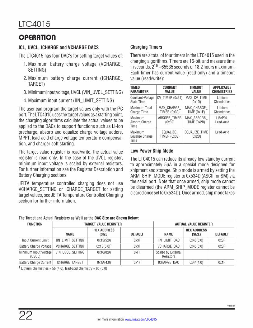
OPERATIONICL, UVCL, ICHARGE and VCHARGE DACS
The LTC4015 has four DAC’s for setting target values of:
1. Maximum battery charge voltage (VCHARGE_ SETTING)
2. Maximum battery charge current (ICHARGE_ TARGET)
3. Minimum input voltage, UVCL (VIN_UVCL_SETTING)
4. Maximum input current (IIN_LIMIT_SETTING)
The user can program the target values only with the I2C port. The LTC4015 uses the target values as a starting point, the charging algorithms calculate the actual values to be applied to the DACs to support functions such as Li-Ion precharge, absorb and equalize charge voltage adders, MPPT, lead-acid charge voltage temperature compensa-tion, and charger soft starting.
The target value register is read/write, the actual value register is read only. In the case of the UVCL register, minimum input voltage is scaled by external resistors. For further information see the Register Description and Battery Charging sections.
JEITA temperature controlled charging does not use VCHARGE_SETTING or ICHARGE_TARGET for setting target values, see JEITA Temperature Controlled Charging section for further information.
Charging Timers
There are a total of four timers in the LTC4015 used in the charging algorithms. Timers are 16-bit, and measure time in seconds. 216 = 65535 seconds or 18.2 hours maximum. Each timer has current value (read only) and a timeout value (read/write):
TIMED PARAMETER
CURRENT VALUE
TIMEOUT VALUE
APPLICABLE CHEMISTRIES
Constant-Voltage State Time
CV_TIMER (0x31) MAX_CV_TIME (0x1D)
Lithium Chemistries
Maximum Total Charge Time
MAX_CHARGE_TIMER (0x30)
MAX_CHARGE_TIME (0x1E)
Lithium Chemistries
Maximum Absorb Charge Time
ABSORB_TIMER (0x32)
MAX_ABSORB_TIME (0x2B)
LiFeP04, Lead-Acid
Maximum Equalize Charge Time
EQUALIZE_TIMER (0x33)
EQUALIZE_TIME (0x2D)
Lead-Acid
Low Power Ship Mode
The LTC4015 can reduce its already low standby current to approximately 5μA in a special mode designed for shipment and storage. Ship mode is armed by setting the ARM_SHIP_MODE register to 0x534D (ASCII for SM) via the serial port. Note that once armed, ship mode cannot be disarmed (the ARM_SHIP_MODE register cannot be cleared once set to 0x534D). Once armed, ship mode takes
The Target and Actual Registers as Well as the DAC Size are Shown Below:FUNCTION TARGET VALUE REGISTER ACTUAL VALUE REGISTER
NAMEHEX ADDRESS
(SIZE) DEFAULT NAMEHEX ADDRESS
(SIZE) DEFAULT
Input Current Limit IIN_LIMIT_SETTING 0x15(5:0) 0x3F IIN_LIMIT_DAC 0x46(5:0) 0x3F
Battery Charge Voltage VCHARGE_SETTING 0x1B(5:0)1 0x3F VCHARGE_DAC 0x45(5:0) 0x3F
Minimum Input Voltage (UVCL)
VIN_UVCL_SETTING 0x16(8:0) 0xFF Scaled by External Resistors
Battery Charge Current ICHARGE_TARGET 0x1A(4:0) 0x1F ICHARGE_DAC 0x44(4:0) 0x1F1 Lithium chemistries = 5b (4:0), lead-acid chemistry = 6b (5:0)
LTC4015
234015fb
For more information www.linear.com/LTC4015
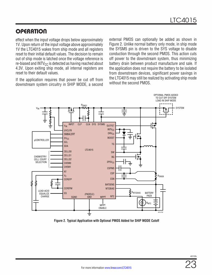
OPERATIONeffect when the input voltage drops below approximately 1V. Upon return of the input voltage above approximately 1V the LTC4015 wakes from ship mode and all registers reset to their initial default values. The decision to remain out of ship mode is latched once the voltage reference is re-biased and INTVCC is detected as having reached about 4.3V. Upon exiting ship mode, all internal registers are reset to their default values.
If the application requires that power be cut off from downstream system circuitry in SHIP MODE, a second
external PMOS can optionally be added as shown in Figure 2. Unlike normal battery only mode, in ship mode the SYSM5 pin is driven to the SYS voltage to disable conduction through the second PMOS. This action cuts off power to the downstream system, thus minimizing battery drain between product manufacture and sale. If the application does not require the battery to be isolated from downstream devices, significant power savings in the LTC4015 may still be realized by activating ship mode without the second PMOS.
Figure 2. Typical Application with Optional PMOS Added for SHIP MODE Cutoff
LTC4015
VIN
UVCLFB
µCONTROLLER
VIN
SMBALERT
DVCC
SCL
SDA
CELLS0
CELLS1
CELLS2
CHEM0
CHEM1
RT
VC
CCREFP
CCREFM
EQ
INFET CLP
RSNS1
CLN SYS SYSM5
4015 F02
OUTFET
SYSTEM
OPTIONAL PMOS ADDEDTO CUT OFF SYSTEMLOAD IN SHIP MODE
INTVCC
DRVCC
BOOST
TG
SW
BG
2P5VCC
CSPM5
CSP
CSN
RNTCBIAS
RSNSB
BATSENS
NTCBIAS
NTC
CHEMISTRY/CELL COURT
SELECTION
LEAD-ACIDEQUALIZE
CHARGE(PADDLE)
GNDSGND MPPT
MPPTENABLE
RNTC
BATTERYPACK
T

LTC4015
244015fb
For more information www.linear.com/LTC4015
OPERATIONCells Selection
Number of series cells selection is made using the CELLS2, CELLS1, and CELLS0 pins. For lithium chem-istries the LTC4015 allows charging of up to nine series cells. For lead-acid there are only three valid selections 3, 6 or 12 cells corresponding to 6, 12, and 24V batteries respectively. Note that number of cells multiplied by their expected maximum cell voltage during charging cannot exceed VIN – 200mV. With VIN/VSYS limited to 35V as an upper bound for VBAT, at nine cells the maximum V/cell would be 3.89V. In practice the 3.89V/cell will be lower, due to several factors including; input ideal diode drop (VIN – VSYS) and switcher max duty cycle. These pins should be hard wired to GND(L), INTVCC(H), or left open (Z). The LTC4015 does not monitor or balance individual cells – the full battery stack voltage is divided by number of cells (V/cell) for simplicity only. The 4015 is not a substitute for pack protection!
NUMBER OF CELLS CELLS2 CELLS1 CELLS0
Invalid L L L
1 L L H
2 L H L
3 L H H
4 L L Z
5 L Z L
6 L H Z
7 L Z H
8 L Z Z
9 H L L
Invalid H L H
Invalid H H L
12* H H H
* Lead-acid only
Chemistry Selection
Chemistry selection is made using the CHEM1 and CHEM0 pins. These are three-state pins used by the LTC4015 to select of one of nine chemistry specific charging algorithms. These pins should be hard wired to GND(L), INTVCC(H), or left open (Z).
CHEMISTRY CHEM1 CHEM0Li-Ion Programmable L L
Li-Ion 4.2V/Cell Fixed H H
Li-Ion 4.1V/Cell Fixed L Z
Li-Ion 4V/Cell Fixed Z L
LiFePO4 Programmable L H
LiFePO4 Fixed Fast Charge H Z
LiFePO4 Fixed Standard Charge Z H
Lead-Acid Fixed Z Z
Lead-Acid Programmable H L
Li-Ion/LiFePO4 Battery Charging
It is the responsibility of the user of the LTC4015 to consult with the battery manufacturer to determine the recommended charging parameters for a particular battery. Battery allowable temperature range while charging and any required charging parameter temperature coefficients also need to be considered.

LTC4015
254015fb
For more information www.linear.com/LTC4015
OPERATION
Table 5. Li-Ion Charging Parameters
CHARGING ALGORITHM
ICHARGE_TARGET
VCHARGE (PER CELL)
CV TIMER TERM ENABLE
MAX CV TIME
C/x TERM ENABLE
C/x THRESH JEITA
MAX CHARGE
TIME
LOW BAT PRECHARGE
CURRENT
LOW BAT THRESHOLD (PER CELL)
Li-Ion Programmable
32mV/RSNSB
14.201 Yes 4 Hours No 10% Y 18 Hrs ~10%2 2.9V
Li-Ion 4.2V/cell Fixed
32mV/RSNSB
14.201 Yes 4 Hours No – Y 18 Hrs ~10%2 2.9V
Li-Ion 4.1V/cell Fixed
32mV/RSNSB
14.101 Yes 4 Hours No – Y 18 Hrs ~10%2 2.9V
Li-Ion 4V/cell Fixed
32mV/RSNSB
14.001 Yes 4 Hours No – Y 18 Hrs ~10%2 2.9V
Li-Ion/Charging Parameters
Table 5 shows Li-Ion charging parameters. For Li-Ion programmable, defaults values are shown.
Bold parameters are I2C programmable in Li-Ion programmable mode only. ICHARGE_TARGET and VCHARGE_SETTING values are at 25°C if JEITA is en-abled1. Shown in Figure 3 is an example of a Li-Ion battery charging profile. Shown in Table 6 are the Li-Ion program-mable I2C configurable charging parameters.
Table 6. Li-Ion Programmable I2C Configurable ParametersPROGRAMMABLE MODE PARAMETER RANGE BITS RESOLUTION
ICHARGE_TARGET1 1mV to 32mV/RSNSB
5 1mV/RSNSB
VCHARGE_SETTING1 3.8125V to 4.2V/Cell
5 12.5mV
MAX_CV_TIME 0 to 65535 16 1 Second
en_jeita 0, 1 1 1 = Enable
en_c_over_x_term 0, 1 1 1 = Enable
C_OVER_X_THRESHOLD 0mV to 32mV/RSNSB
16 1.465µV/RSNSB
MAX_CHARGE_TIME 0 to 65535 16 1 Second
Notes1) When JEITA is enabled (en_jeita=1), ICHARGE_TARGET and
VCHARGE_SETTING are controlled by the JEITA temperature controlled charging algorithm, as described in the descriptions for ICHARGE_JEITA_n and VCHARGE_JEITA_n.
2) Precharge current is 10% of ICHARGE_TARGET, rounded down to the next LSB.
Figure 3. Li-Ion 4.2V/Cell Fixed Charging Profile
TIME (hr)
V BAT
(VCE
LL) ICHG (A)
4015 F03
4.5
4.0
3.0
2.5
2.0
1.5
1.0
0.5
3.5
0
12
9
6
3
00 1 4 5 632
VBATICHG
CC_CV/CC
CC_CV/CV
4HOUR CV TIMERTERMINATION
TEXT INDICATES VALUES REPORTED IN REGISTERS:CHARGER_STATE/CHARGE_STATUS

LTC4015
264015fb
For more information www.linear.com/LTC4015
OPERATIONLiFePO4 Charging ParametersTable 7 shows LiFePO4 charging parameters. For LiFePO4 programmable, defaults values are shown. Bold parameters are I2C programmable in LiFePO4 programmable mode only. ICHARGE_TARGET and VCHARGE_SETTING values
Table 7. LiFePO4 Charging Parameters
CHARGING ALGORITHM
ICHARGE_ TARGET
VABSORB, MAX_
ABSORB_ TIME IN
MINUTESVCHARGE
(PER CELL)
CV TIMER TERM
MAX CV TIME C/x TERM
C/x THRESH JEITA
MAX CHARGE TIME
LiFePO4 Programmable 32mV/RSNSB
1No Absorb
Phase3.601 Yes 1 Hour No 10% Y 18 Hrs
LiFePO4 Fixed Standard Charge
32mV/RSNSB
1No Absorb
Phase3.601 Yes 1 Hour No – Y 18 Hrs
LiFePO4 Fixed Fast Charge
32mV/RSNSB
13.8, 15 3.601 Yes 1 Hour No 10%
(Absorb)Y 18 Hrs
1: When JEITA is enabled ICHARGE_TARGET and VCHARGE_SETTING are overridden and controlled by the JEITA temperature qualified charging algorithm.
are at 25°C when JEITA is enabled. Shown in Table 8 are the LiFePO4 programmable I2C configurable charging parameters. Shown in Figure 4 is the LiFePO4 fixed fast charge charging profile.
Table 8. LiFePO4 Programmable I2C Configurable ParametersPROGRAMMABLE MODE PARAMETER RANGE BITS RESOLUTIONICHARGE_TARGET1 1mV to
32mV/RSNSB
5 1mV/RSNSB
VABSORB_DELTA 0V to 0.4V 5 12.5mV
MAX_ABSORB_TIME 0 to 65535 16 1 Second
VCHARGE_SETTING1 3.4125V to 3.8V/Cell
5 12.5mV
MAX_CV_TIME 0 to 65535 16 1 Second
en_jeita 0,1 1 1 = Enable
en_c_over_x_term 0,1 1 1 = Enable
C_OVER_X_THRESHOLD 0mV to 32mV/RSNSB
16 1.465µV/RSNSB
MAX_CHARGE_TIME 0 to 65535 16 1 Second
LiFePO4_RECHARGE_THRESHOLD 0 to 4.2V/Cell 16 192.26µV
Notes1: When JEITA is enabled ICHARGE_TARGET and VCHARGE_SETTING
are overridden and controlled by the JEITA temperature qualified charging algorithm.
Figure 4. LiFePO4 Fast Charge Charging Profile
TIME (min)
V BAT
(VCE
LL) ICHG (A)
4015 F04
4.5
4.0
3.0
2.5
2.0
1.5
1.0
0.5
3.5
0
12
9
6
3
00 5 20 25 301510
VBATICHG
ABSORB/CC CC_CV/CV
ABSORB/CV
TEXT INDICATES VALUES REPORTED IN REGISTERS:CHARGER_STATE/CHARGE_STATUS
CV TIMER TERMINATIONAFTER ONE HOUR IN CC_CV/CV PHASE

LTC4015
274015fb
For more information www.linear.com/LTC4015
OPERATIONLi-Ion/LiFePO4 Battery Charger Operation
The LTC4015 provides full featured, inherently safe, constant-current/constant-voltage Li-Ion/LiFePO4 battery charging. Features include battery presence detection, automatic recharge, maximum charge time safety timer, precharge (Li-Ion only), rapid absorb charge (LiFePO4 only), programmable CV timer and C/x termination, therm-istor temperature controlled charging, programmable end-of-charge indication, programmable charge voltage, programmable charge current, J.E.I.T.A. support, battery series resistance measurement, detailed status reporting, and programmable interrupt generation.
LTC4015 Charge Algorithm Overview
The LTC4015 charge algorithms are based on a constant-current constant-voltage charging (CC-CV)technique. The battery is charged at a constant-current (CC) until the battery reaches its charge voltage (VCHARGE) whereupon the delivered charge current is automatically reduced to maintain the battery at a constant VCHARGE (CV). The LTC4015 does not monitor or balance individual cells – the full battery stack voltage is divided by number of cells (V/cell) for simplicity only. The 4015 is not a substitute for pack protection!
Under voltage current limiting (UVCL) is used to automati-cally reduce charge current to help keep VIN from falling below a minimum voltage. Input current limiting (ICL) is used to automatically limit charge current to help keep Input current below a maximum level. However, UVCL and ICL can only reduce charge current. The total load current from VIN cannot be limited by the LTC4015 if the load on the system exceeds the ICL setpoint.
Li-Ion Charge Algorithm Overview
(See Figure 5A for Li-Ion battery charging state diagram)
The charge algorithm begins with a battery detection test and proceeds to constant-current constant-voltage (CC-
CV) charging. If the Li-Ion battery voltage is very low the charger will charge at a reduced (precharge) CC rate until the battery voltage reaches an acceptable level. Then it will be charged at the full CC rate. CC-CV charging continues until the charge cycle terminates based on time (default) or battery current (C/x for Li-Ion programmable option).
LiFePO4 Charge Algorithm (without Absorption Phase) Overview
(See Figure 5B for LiFePO4 battery charging state diagram)
The charge algorithm begins with a battery detection test and proceeds to constant-current constant-voltage (CC-CV) charging. CC-CV charging continues until the charge cycle terminates based on time in CV mode (default) or battery current (C/x for LiFePO4 programmable option). Remaining in constant-voltage mode without termination is also a LiFePO4 programmable option.
LiFePO4 Charge Algorithm (with Absorption Phase) Overview
(See Figure 5B for Li-FePO4 battery charging state diagram)
An absorb phase can allow accelerated charging by raising the charge voltage, which may result in a higher CC rate, for a portion of the charge cycle. The charge algorithm begins with a battery detection test and proceeds to CC-CV charging with a charge voltage of VABSORB, which is an absorb delta added to VCHARGE. CC-CV absorption charging continues until the VABSORB is reached and charge current has dropped below the C/x threshold, or the maximum absorb phase time has passed. Upon exiting the absorb phase the charge voltage is reduced from VABSORB to VCHARGE. CC-CV charging continues until the charge cycle terminates based on time in CV mode (default) or charge current (C/x) (LiFePO4 programmable option). Remaining in constant-voltage mode without termination is also a LiFePO4 programmable option.

LTC4015
284015fb
For more information www.linear.com/LTC4015
OPERATION
Figure 5A. Li-Ion Battery Charging State Diagram
CHARGER_SUSPENDED*
BATTERYDETECTION
SHORTEDBATTERY
NO BATTERY 30 SECONDTIME OUT
BAT_MISSING_FAULT
PRECHARGE
BATTERY VOLTAGE > 2.9 V/CELL
MAX_CHARGE_TIME_FAULT
MAX_CHARGE_TIMEPASSEDVBAT < 35%
OF VCHARGE
NTC_RATIOBETWEEN JEITA_T7AND JEITA_T1
* NOTE: ALL STATES RETURN TO CHARGER SUSPENDED IF ANY OF THE FOLLOWING OCCUR: A. THE INPUT VOLTAGE VIN FALLS TO WITHIN 100mV OF THE BATSENS PIN VOLTAGE. B. SUSPEND_CHARGER IS WRITTEN TO 1 VIA THE SERIAL PORT. C. A SYSTEM FAULT OCCURS (VIN OVERVOLTAGE LOCKOUT, 2P5VCC UNDERVOLTAGE LOCKOUT, INTVCC UNDERVOLTAGE LOCKOUT, DRVCC UNDERVOLTAGE LOCKOUT. THERMAL SHUTDOWN, MISSING RT RESISTOR, OR INVALID COMBINATION OF CELLS PINS).
NTC_RATIOBELOW JEITA_T7OR ABOVE JEITA_T1
TO NTCPAUSE
BATTERY VOLTAGE> 2.85V/CELL
MAX_CHARGE_TIMER STARTS
C_OVER_X_TERM
4015 F05a
MAX_CV_TIME PASSEDWITH BATTERY ATVCHARGE (CV)
BATTERY AT VCHARGE (CV)—AND—ICHG < C_OVER_X_THRESHOLD—AND—EN_C_OVER_X_TERM = 1
RECHARGE THRESHOLDREACHED
RECHARGE THRESHOLDREACHED
BATTERYVOLTAGE STABLE
BATTERY VOLTAGE < 2.85 VCELL
CC_CV_CHARGE
BAT_SHORT_FAULT
NTC_PAUSE
NTC_RATIOOUT OF RANGE
TO BAT_MISSING_FAULT
RETURN TO PREVIOUSCHARGE STATE
NTC_RATIOBELOW JEITA_T7OR ABOVE JEITA_T1
TO NTCPAUSE
TIMER_TERM

LTC4015
294015fb
For more information www.linear.com/LTC4015
OPERATION
Figure 5B. LiFePO4 Battery Charging State Diagram
CHARGER_SUSPENDED*
BATTERYDETECTION
SHORTEDBATTERY
NO BATTERY 30 SECONDTIME OUT
BAT_MISSING_FAULT
ABSORBCHARGE
ABSORB_TIME PASSED—OR—(ABSORB VOLTAGE REACHED AND ICHG < C_OVER_X_THRESHOLD)
MAX_CHARGE_TIME_FAULT
MAX_CHARGE_TIMEPASSEDVBAT < 35%
OF VCHARGE
NTC_RATIOBETWEEN JEITA_T7AND JEITA_T1
* NOTE: ALL STATES RETURN TO CHARGER SUSPENDED IF ANY OF THE FOLLOWING OCCUR: A. THE INPUT VOLTAGE VIN FALLS TO WITHIN 100mV OF THE BATSENS PIN VOLTAGE. B. SUSPEND_CHARGER IS WRITTEN TO 1 VIA THE SERIAL PORT. C. A SYSTEM FAULT OCCURS (VIN OVERVOLTAGE LOCKOUT, 2P5VCC UNDERVOLTAGE LOCKOUT, INTVCC UNDERVOLTAGE LOCKOUT, DRVCC UNDERVOLTAGE LOCKOUT. THERMAL SHUTDOWN, MISSING RT RESISTOR, OR INVALID COMBINATION OF CELLS PINS).
NTC_RATIOBELOW JEITA_T7OR ABOVE JEITA_T1
TO NTCPAUSE
C_OVER_X_TERM
4015 F05a
MAX_CV_TIME PASSEDWITH BATTERY ATVCHARGE (CV)—AND—NOT (MAX_CV_TIME = 0)
BATTERY AT VCHARGE (CV)—AND—ICHG < C_OVER_X_THRESHOLD—AND—EN_C_OVER_X_TERM = 1
RECHARGE THRESHOLDREACHED
RECHARGE THRESHOLDREACHED
BATTERYVOLTAGE STABLE
MAX_CHARGE_TIMER STARTS
VABSORB_DELTA > 0ABSORB_TIMER STARTS
CC_CV_CHARGE
BAT_SHORT_FAULT
NTC_PAUSE
NTC_RATIOOUT OF RANGE
TO BAT_MISSING_FAULT
RETURN TO PREVIOUSCHARGE STATE
NTC_RATIOBELOW JEITA_T7OR ABOVE JEITA_T1
TO NTCPAUSE
TIMER_TERM

LTC4015
304015fb
For more information www.linear.com/LTC4015
OPERATIONBattery Detection
The LTC4015 begins a charging cycle by performing a two to four second battery detection test, during which a 1mA load is drawn from the battery. If the battery volt-age remains stable during the battery detection test, the LTC4015 proceeds with battery charger soft-start. If the battery voltage does not remain stable, the LTC4015 proceeds with a battery open/short test. The battery is charged at minimum charge current for one to two seconds. If the battery voltage as a result of this brief charging is within a reasonable range the LTC4015 will proceed with a battery charger soft-start. A battery open fault will also occur if the NTC resistor is open or has a very high value. A programmable interrupt can be set to alert the system if a battery detection fault has occurred.
Battery Charger Soft-Start
The LTC4015 soft starts by ramping ICHARGE_DAC from 0 to ICHARGE_TARGET at a nominal rate of 400µs per ICHARGE_TARGET LSB. This results in a maximum soft-start time of 31 • 400µs = 12.4ms.
Maximum Charge Time
The LTC4015, for charging batteries of Lithium chemistries, provides a maximum charge time safety timer. The MAX_CHARGE_TIMER starts with the battery charger soft-start after battery detection. If the total time charging the battery exceeds MAX_CHARGE_TIME, the charger will enter the MAX_CHARGE_TIME FAULT state and cease charging. This fault state can only be exited in normal operation if the battery voltage is less than 35% of VCHARGE, where upon a new charge cycle begins and the timer reset. The timer is reset upon timer or C/x termination. The MAX_CHARGE_TIME fault state can also be exited as a result of the input voltage VIN falling to within 100mV of the BATSENS pin voltage, SUSPEND_CHARGER is written to a 1 via the serial port or a system fault occurs.
Low Battery/Pre-Charge; Li-Ion
When a Li-Ion battery charge cycle begins, the LTC4015 first determines if the battery is deeply discharged. If the battery voltage is below 2.85V per cell (VBAT_FILT below 14822) and BATSENS pin is above 2.6V then the LTC4015 begins charging by applying a preconditioning charge equal to ICHARGE_TARGET/10 (rounded down to the next LSB), and reporting precharge = 1. When the battery voltage exceeds 2.9V per cell (VBAT_FILT above 15082), the LTC4015 proceeds to the constant-current/constant-voltage charging phase (cc_cv_charge = 1).
Should the BATSENS pin voltage be lower than 2.4V, the switching charger operates in constant peak current mode, where the peak current is 7mV/RSNSB. Exact average cur-rent value depends on a number of factors including input voltage, battery voltage and inductance value. When the BATSENS pin voltage is higher than 2.6V, normal charg-ing proceeds.
Low Battery; LiFePO4
Low battery for LiFePO4 chemistry is the same as Li-Ion with the exception that there is no precon-ditioning charge phase; charge current is set by ICHARGE_TARGET.
However, if the BATSENS pin voltage is lower than 2.4V, the switching charger operates in constant peak current mode, where the peak current is 7mV/RSNSB. Exact average current value depends on a number of factors including input voltage, battery voltage and inductance value. When the BATSENS pin voltage is higher than 2.6V, normal charging proceeds.
LiFePO4 Absorb Charge
The LTC4015 can optionally perform an accelerated absorb charge cycle on LiFePO4 batteries. If VABSORB_DELTA is greater than zero, the LTC4015 begins charging with an absorb charge phase, and reports absorb_charge = 1

LTC4015
314015fb
For more information www.linear.com/LTC4015
OPERATIONvia the serial port. During absorb charging, the LTC4015 charges at a constant-current ICHG, with a target set by ICHARGE_TARGET and RSNSB, unless one of the following conditions occurs:
a) The battery voltage reaches the absorb target voltage (determined by VCHARGE_SETTING + VABSORB_DELTA, limited to a maximum of 3.8V/cell), indicated by constant_voltage=1
b) Input current limit (IIN_LIMIT_SETTING) is reached, indicated by iin_limit_active=1
c) The UVCLFB pin voltage falls to the undervoltage current limit (VIN_UVCL_SETTING) ), indicated by vin_uvcl_ac-tive=1
If either the input current limit or the undervoltage current limit is activated, the LTC4015 will limit charge current and will attempt to regulate at the input current or input voltage limit level, as permitted by the input source and system load.
LiFePO4 Absorb Phase Ends After Either:
a) MAX_ABSORB_TIME has passed
b) The battery voltage reaches absorb target voltage (as determined by VCHARGE_SETTING+VABSORB_DELTA, limited to a maximum of 3.8V/cell), indicated by constant_voltage=1, and IBAT falls below C_OVER_X_THRESHOLD. When the absorb phase ends, the LTC4015 proceeds to the CC-CV charging phase.
Constant-Current/Constant-Voltage (CC-CV) Charging Constant-Current
When the battery voltage is above 2.9V per cell, the charger will attempt to deliver the programmed charge current ICHG, as set by ICHARGE_TARGET and RSNSB, in constant-current mode. Depending on available input power and external load conditions, the battery charger may not be able to charge at the full programmed rate. If input current limit is reached, the system load will always be prioritized over the battery charge current. Likewise, the
input undervoltage control loop will always be observed and may limit the power available to charge the battery. When system loads permit, battery charge current will be maximized.
The upper limit of charge current ICHG is programmed by the combination of the current sense resistor (RSNSB) from CSP to CSN and a servo voltage of 32mV or a value programmed via the serial port (see register descriptions for ICHARGE_TARGET and icharge_jeita_n). The voltage across RSNSB divided by its value determines the maximum possible charge current. The maximum servo voltage that can be programmed is 32mV. A 4mΩ resistor, for example, would have an upper limit charge current of 8A.
Independent of whether or not the charge current loop is controlling the switching charger, the voltage across the RSNSB will represent the actual charge current delivered to the battery. The voltage across RSNSB is measured by the LTC4015’s onboard measurement system and is available via the serial port in register IBAT.
RSNSB should be set based on the maximum charge current of the battery without regard to source or load limitations from any other control loop. The multiple control loop architecture of the LTC4015 will correct for any discrepancies, always sorting out the optimal transfer of power to the battery.
Battery Series Resistance (BSR) Measurement
The LTC4015 can optionally measure the series resistance of the battery. If run_bsr is set to 1 the LTC4015 momentarily suspends the battery charger and calculates the battery series resistance by dividing the change (charging vs charger suspended) in battery voltage by the change in charge current (ICHARGE_BSR). The per cell resistance value is reported in the BSR register and the change in charge current is reported in the ICHARGE_BSR register via the serial port. The LTC4015 resets run_bsr to 0 after the BSR measurement is complete. The battery series resistance value is proportional to the charge current

LTC4015
324015fb
For more information www.linear.com/LTC4015
OPERATIONsense resistor, RSNSB, and can be computed in Ω from BSR • RSNSB/500. Note that the resistance reported in the BSR register must be multiplied by the total number of cells to calculate total battery series resistance. The higher ICHARGE_BSR (charge current) when a BSR measurement is requested, the more accurate the BSR measurement will be. Very low values of ICHARGE_BSR may significantly impact the accuracy of the BSR measurement. Setting run_bsr to a 1 will not turn the charger on, if the charger is suspended or in a termination state, setting run_bsr = 1 results in the BSR measurement request being queued and run after the soft-start of the next charge cycle.
Battery Charge Voltage Regulation, Constant-Voltage
Once the BATSENS voltage reaches the preset charge volt-age, the switching charger will reduce its output power, holding the battery voltage steady. The charge current will decrease naturally toward zero providing inherently safe operation by preventing the battery from being over-charged. Multiple charge voltage settings are available for final charge voltage selection via the serial port. While charge voltage trade-offs can be made to preserve battery life or maximize capacity, it is not possible for the LTC4015 to be set to a charge voltage that is dangerously high or inconsistent with the battery’s chemistry.
Li-Ion LiFePO4 Full Capacity Charge Indication (C/x) and Charger Termination
The battery charge cycle will terminate at the expiration of a built-in programmable CV termination safety timer (CV_TIMER). When the voltage on the battery reaches the programmed charge voltage, the safety timer is started. After the safety timer expires, charging of the battery will discontinue and no more current will be delivered. The safety timer’s default expiration time may be altered via the serial port. For Li-Ion cells the timer termination feature cannot be disabled. For LiFePO4 cells, timer termination can be disabled by setting MAX_CV_TIME to zero, in this case, if C/x termination is not enabled, charging will not terminate. C/x termination cannot be enabled in fixed chemistry algorithms.
In addition, by monitoring the charge current and other states of the system, the LTC4015 determines when the battery has reached a given state of charge. Specifically, programmable C/x detection in constant-voltage mode determines when the charge current has naturally dropped to a given fraction of its full-scale current. If C/x termination is enabled the charge cycle will end when C/x is reached, or when then safety timer expires, whichever occurs first. C/x termination is disabled by default. The LTC4015 can optionally be configured via the serial port to generate an interrupt and terminate charging when the C/x threshold is reached.
The LTC4015 terminates charging by disabling the switch-ing controller, when this occurs the SW node goes HI Z.
Li-Ion LiFePO4 Automatic Recharge
After the battery charger terminates, it will remain off, drawing only a small amount of current from the battery. If the portable product remains in this state long enough, the battery will eventually self discharge. To ensure that the battery is always topped off, a new charge cycle will automatically begin when the battery voltage falls below approximately 97.5% of the programmed charge voltage for Li-Ion and 3.35V/cell for LiFePO4(3.35V/cell is the default for LiFePO4_RECHARGE_THRESHOLD in LiFePO4 programmable mode). The termination safety timer will also reset back to zero. A new charge cycle will also be initiated if input power is cycled or if the charger is momentarily disabled using the serial port (suspend_charger set to 1, then set to 0).
J.E.I.T.A. Temperature Controlled Charging
For lithium chemistries, a measurement and control system has been included to enable compliance with the Japan Electronics and Information Technology Industries Association guidelines on battery charging. Specifically a very flexible multi-point temperature-voltage-current

LTC4015
334015fb
For more information www.linear.com/LTC4015
OPERATIONprofile can be programmed into the LTC4015 to ensure that optimum charging parameters as a function of temperature are always used. Figure 6 illustrates an example of the JEITA system available in the LTC4015. There are seven distinct temperature regions programmed by the six temperature set points JEITA_T1-JEITA_T6. For each of the temperature regions, the charge current and charge voltage can be programmed within the limits set by VCSP–CSN/RSNSB (ICHARGE) and battery charge voltage (VCHARGE) for a selected chemistry code.
When JEITA is enabled, charge current is controlled by ICHARGE_DAC, which in turn is set by icharge_jeita_n of the applicable JEITA region. Writing ICHARGE_TARGET has no effect, as it will be overwritten by JEITA. Likewise VCHARGE is controlled by VCHARGE_DAC which in turn is set by vcharge_jeita_n of the applicable JEITA region.
The LTC4015 provides temperature controlled charging if a grounded thermistor and a bias resistor are connected to the NTCBIAS and NTC pins. Charging is paused if the temperature rises above a programmable upper limit or falls below a programmable lower limit.
If the application does not require temperature controlled charging then the thermistor should be replaced with a resistor of equal value to bias resistor RNTCBIAS, for example, 10kΩ.
Figure 6. Default JEITA Temperature Profile, Showing Values for Li-Ion Fixed 4.2V
TEMPERATURE (°C)
V BAT
(VCE
LL)
CHARGE CURRENT (mV/R
SENSE )
4015 F06
4.5
T1 T2 T3 T5T4 T6
4.0
3.0
2.5
2.0
1.5
1.0
0.5
3.5
0
45
40
30
25
20
15
10
05
35
00 10 40 50 603020
CHARGE VOLTAGECHARGE CURRENT
The values for the JEITA registers are shown in the tables below. The bold values in the tables are programmable when using Li-Ion programmable or LiFePO4 program-mable chemistry selections.
The JEITA_Tn registers determine the NTC_RATIO values for the breakpoints between regions. The corresponding temperature values assume a thermistor β value of 3490k, such as provided by a Vishay NTCS0402E3103FLT or NTHS0402N02N1002JE. For other thermistors, one or two inexpensive low temperature coefficient resistors can generally be added to the circuit to adjust the thermistor’s biasing (see the section NTC Resistor in Applications Information for details).
Table Illustrates the JEITA Values That Can Be Programmed Via the Serial Port.REGION 1 REGION 2 REGION 3 REGION 4 REGION 5 REGION 6 REGION 7
JEITA_T1 JEITA_T2 JEITA_T3 JEITA_T4 JEITA_T5 JEITA_T6
CHARGER OFF
icharge_jeita_2 icharge_jeita_3 icharge_jeita_4 icharge_jeita_5 icharge_jeita_6 CHARGER OFFvcharge_jeita_2 vcharge_jeita_3 vcharge_jeita_4 vcharge_jeita_5 vcharge_jeita_6

LTC4015
344015fb
For more information www.linear.com/LTC4015
Table Default Values for JEITA ParametersREGION 1 REGION 2 REGION 3 REGION 4 REGION 5 REGION 6 REGION 7
JEITA_T1 = JEITA_T2 = JEITA_T3 = JEITA_T4 = JEITA_T5 = JEITA_T6 = 0x3F00 (0°C) 0x372A (10°C) 0x1F27 (40°C) 0x1BCC (45°C) 0x18B9 (50°C) 0x136D (60°C)
CHARGER OFF
icharge_jeita_2 icharge_jeita_3 icharge_jeita_4 icharge_jeita_5 icharge_jeita_6 CHARGER OFFvcharge_jeita_2 vcharge_jeita_3 vcharge_jeita_4 vcharge_jeita_5 vcharge_jeita_6
Li-Ion Programmable
CHARGER OFF
16mV/RSNSB 32mV/RSNSB 32mV/RSNSB 16mV/RSNSB 16mV/RSNSB CHARGER OFF4.20V 4.20V 4.10V 4.10V 4.05V
Li-Ion Fixed 4.2V
CHARGER OFF
16mV/RSNSB 32mV/RSNSB 32mV/RSNSB 16mV/RSNSB 16mV/RSNSB CHARGER OFF4.20V 4.20V 4.10V 4.10V 4.05V
Li-Ion Fixed 4.1V
CHARGER OFF
16mV/RSNSB 32mV/RSNSB 32mV/RSNSB 16mV/RSNSB 16mV/RSNSB CHARGER OFF4.10V 4.10V 4.00V 4.00V 3.95V
Li-Ion Fixed 4.0V
CHARGER OFF
16mV/RSNSB 32mV/RSNSB 32mV/RSNSB 16mV/RSNSB 16mV/RSNSB CHARGER OFF4.00V 4.00V 3.90V 3.90V 3.85V
LiFePO4 Programmable
CHARGER OFF
16mV/RSNSB 32mV/RSNSB 32mV/RSNSB 16mV/RSNSB 16mV/RSNSB CHARGER OFF3.60V 3.60V 3.50V 3.50V 3.45V
LiFePO4 Fixed Fast and Fixed Standard Charge
CHARGER OFF
16mV/RSNSB 32mV/RSNSB 32mV/RSNSB 16mV/RSNSB 16mV/RSNSB CHARGER OFF3.60V 3.60V 3.50V 3.50V 3.45V
OPERATION
Lead-Acid Battery Charging
It is the responsibility of the user of the LTC4015 to consult with the battery manufacturer to determine the recommended charging parameters for a particular battery. Battery allowable temperature range while charging and any required charging parameter temperature coefficients also need to be considered.
An example of charging profile (battery voltage and cur-rent vs. time) for a lead-acid battery is shown in Figure 7.
Lead-Acid Charging Parameters
Following is a table of lead-acid charging parameters. For lead-acid programmable, default values are shown. Bold parameters are programmable via the serial port in lead-acid programmable mode only. All voltages are per cell at 25°C.
Figure 7. Example Charging Profile for a Lead-Acid Battery
TIME (hrs)
CC-CV/CV
ABSORB/CV
ABSORB/CC(ALSO CALLED
BULK CHARGING)TEXT INDICATES VALUES REPORTED IN REGISTERS:CHARGER_STATE/CHARGE_STATUS
EQUALIZE/CC
EQUALIZE/CV
V BAT
(VCE
LL) ICHG (A)
4015 F07
3.0
2.5
2.0
1.5
1.0
0.5
0
12
8
6
4
2
10
00 1 32 TEQ+2TEQ TEQ+4
VBATICHG
CC-CV/CV

LTC4015
354015fb
For more information www.linear.com/LTC4015
OPERATIONUndervoltage current limiting (UVCL) is used to automati-cally reduce charge current to help keep VIN from falling below a minimum voltage. Input current limiting (ICL) is used to automatically limit charge current to help keep input current below a maximum level. However, UVCL and ICL can only reduce charge current. The total load current from VIN cannot be limited by the LTC4015 if the load on SYS exceeds the ICL setpoint.
Figure 8. Lead-Acid Battery Charging State Diagram
Lead-Acid Charging Parameters
CHARGING ALGORITHM
ICHARGE_ TARGET
ABSORB C_OVER_X_THRESHOLD
VEQUALIZE, EQUALIZE TIME
(MINUTES)
VABSORB, MAX ABSORB TIME
(MINUTES)
END ABSORB ON C/x
VCHARGE (PER CELL)
mV/C TEMPCO
TEMPCO ENABLED
Lead-Acid Fixed 32mV/RSNSB 3.2mV/RSNSB 2.60, 60 2.40, 90 Yes 2.20 –3.65 Yes
Lead-Acid Programmable
32mV/RSNSB 3.2mV/RSNSB 2.60,60 2.40, 90 Yes 2.20 –3.65 Yes
PROGRAMMABLE MODE PARAMETER RANGE BITS RESOLUTION
ICHARGE_TARGET 1mV to 32mV/RSNSB
5 1mV/RSNSB
VCHARGE_SETTING 2V to 2.6V/Cell 6 9.523mV
VABSORB_DELTA 0V to 0.6V/Cell 6 9.523mV
VEQUALIZE_DELTA 0V to 0.6V/Cell 6 9.523mV
MAX_ABSORB_TIME 0 to 65535 16 1 Second
EQUALIZE_TIME 0 to 65535 16 1 Second
en_lead_acid_temp_comp 0, 1 1 1 = Enable
C_OVER_X_THRESHOLD1 0mV to 32mV/RSNSB
16 1.465µV/RSNSB
Notes1: In lead-acid mode C_OVER_XTHRESHOLD is used only to terminate
the absorb charge phase.
Lead-Acid Battery Charger Operation
The LTC4015 provides full featured, inherently safe, constant-current/constant-voltage lead-acid battery charging with battery presence detection, equalization, absorb, bad battery detection, thermistor based charge voltage temperature compensation, programmable charge voltage, programmable charge current, battery series resistance measurement, detailed status reporting, and programmable interrupt generation.
LTC4015 Charge Algorithm Overview
The LTC4015 charge algorithms are based on a constant-current constant-voltage charging (CC-CV) technique. The battery is charged at a constant-current (CC) until the battery reaches its charge voltage (VCHARGE) whereupon the delivered charge current is automatically reduced to maintain the battery at a constant VCHARGE (CV).The LTC4015 does not monitor or balance individual cells – the full battery stack voltage is divided by number of cells (V/cell) for simplicity only. The 4015 is not a substitute for pack protection!
Lead Acid Charge Algorithm Overview
(See Figure 8 for lead-acid battery charging state diagram)
The charge algorithm begins with a battery detection test, then proceeds to CC-CV charging with a charge voltage
CHARGER_SUSPENDED*
BATTERYDETECTION
NO BATTERY
SHORTEDBATTERY
BAT_SHORT_FAULT
* NOTE: ALL STATES RETURN TO CHARGER SUSPENDED IF ANY OF THE FOLLOWING OCCUR: A. THE INPUT VOLTAGE VIN FALLS TO WITHIN 100mV OF THE BATSENS PIN VOLTAGE. B. SUSPEND_CHARGER IS WRITTEN TO 1 VIA THE SERIAL PORT. C. A SYSTEM FAULT OCCURS (VIN OVERVOLTAGE LOCKOUT, 2P5VCC UNDERVOLTAGE LOCKOUT, INTVCC UNDERVOLTAGE LOCKOUT, DRVCC UNDERVOLTAGE LOCKOUT. THERMAL SHUTDOWN, MISSING RT RESISTOR, OR INVALID COMBINATION OF CELLS PINS).
ABSORB_TIME PASSEDWITH BATTERY ATABSORB VOLTAGE—OR—(BATTERY AT ABSORB VOLTAGEAND ICHG < C_OVER_X_THRESHOLD)
4015 F08
BATTERYVOLTAGE STABLE
EQ PIN RISINGEDGE DETECTED
EQUALIZE_TIMEPASSED—OR—EQ PIN FALLINGEDGE DETECTED
ABSORB_CHARGE
CC_CV_CHARGE EQUALIZE_CHARGE
BAT_MISSING_FAULT 30 SECOND
TIMEOUT

LTC4015
364015fb
For more information www.linear.com/LTC4015
OPERATIONof VABSORB, which is an absorb delta added to VCHARGE. Following constant-current bulk charging, constant-voltage absorption charging continues until VABSORB is reached and charge current has dropped below the C/x threshold, or the battery absorb charge voltage is reached and the maximum absorb phase time has passed. If neither of the criteria for exiting the absorb charge phase is met then CC-CV charging with VABSORB charge voltage can continue indefinitely. Upon exiting the absorb phase the charge voltage absorb delta is set to zero and CC-CV float charging continues indefinitely.
Upon exiting the absorb phase an equalization charge can be performed upon user request.
Lead Acid Equalization Charge
The equalization charge voltage, VEQUALIZE, can be signifi-cantly higher than the absorption voltage. This aggressive overcharging of the battery can equalize acid concentrations throughout the battery and remove electrode sulfation that may have formed during low charge conditions. Equal-ization can restore battery capacity, but it can also result in battery heating, overcharging of some or all cells and the loss of electrolyte which can lead to battery damage. Equalization is typically not performed with sealed batter-ies because they are usually not re-wettable in the event of electrolyte loss. Due to its aggressive nature, specific equalization frequency, voltage and time duration should be obtained from the battery manufacturer.
Battery Detection
The LTC4015 begins a charging cycle by performing a two to four second battery detection test, during which a 1mA load is drawn from the battery. If the battery volt-age remains stable during the battery detection test, the LTC4015 proceeds with battery charger soft-start. If the battery voltage does not remain stable, the LTC4015 proceeds with a battery open/short test. The battery is charged at minimum charge current for one to two seconds. If the battery voltage as a result of this brief charging is within a reasonable range the LTC4015 will proceed with a battery charger soft-start. A battery open fault will also occur if the NTC resistor is open or has a very high value. A programmable interrupt can be set to alert the system if a battery detection fault has occurred.
Battery Charger Soft-Start
The LTC4015 softs starts by ramping ICHARGE_DAC from minimum to ICHARGE_TARGET at a nominal rate of 400µS per ICHARGE_TARGET LSB. This results in a maximum soft-start time of 31 • 400µS = 12.4mS.
Low Battery
If the BATSENS pin voltage is lower than 2.4V, the switching charger operates in constant peak current mode, where the peak current is 7mV/RSNSB. Exact average current value depends on a number of factors including input voltage, battery voltage and inductance value. When the BATSENS pin voltage is higher than 2.6V, normal charging proceeds.
Absorb Charge
The LTC4015 begins lead-acid battery charging with an absorb charge phase, and reports absorb_charge = 1 via the serial port. During absorb charging, the LTC4015 charges at a constant-current ICHG, with a target set by ICHARGE_TARGET and RSNSB, unless one of the following conditions occurs:
a) The battery voltage reaches the absorb target voltage (VABSORB)(determined by VCHARGE_SETTING+VABSORB_DELTA, limited to a maximum of 2.6V/cell), indicated by constant_voltage=1
b) Input current limit (IIN_LIMIT_SETTING) is reached, indicated by iin_limit_active=1
c) The UVCLFB pin voltage falls to the undervoltage current limit (VIN_UVCL_SETTING), indicated by vin_uvcl_ac-tive=1
If either the input current limit or the input undervoltage current limit is activated, the LTC4015 will limit charge current and will attempt to regulate at the input current limit or input undervoltage limit, as permitted by the input source and system load.
Absorb phase ends after the battery voltage reaches VABSORB and either ABSORB_TIMER reaches MAX_ABSORB_TIME or IBAT falls below C_OVER_X_THRESHOLD. When the absorb phase ends, the LTC4015 proceeds to constant-current/constant-voltage (CC-CV) charge phase.
Constant-Current/Constant-Voltage (CC-CV) Charge:
In CC-CV charging phase, the LTC4015 prevents the

LTC4015
374015fb
For more information www.linear.com/LTC4015
OPERATIONbattery voltage from falling below the charge voltage level, as determined by VCHARGE_SETTING, unless one of the following conditions occurs:
a) The battery charge current ICHG reaches the target set by ICHARGE_TARGET, indicated by constant_current=1
b) Input current limit (IIN_LIMIT_SETTING) is reached, indicated by iin_limit_active=1
c) The UVCLFB pin voltage falls to the undervoltage current limit (VIN_UVCL_SETTING), indicated by vin_uvcl_ac-tive = 1
If either the input current limit or the input undervoltage current limit is activated, the LTC4015 will limit charge current and will attempt to regulate at the input current limit or input undervoltage limit, as permitted by the input source and system load. There is no termination in the charging algorithm for lead-acid; the charger will remain in CV mode as long as input power is available.
Equalization Charge:
If a rising edge is detected on the EQ pin (as reported by the equalize_req bit), the LTC4015 will perform an equalization charge when the charge voltage is reached (constant-voltage = 1) in constant-current/constant-voltage (CC-CV) charge phase. In equalization charging phase, the LTC4015 charges the battery at a constant-current ICHG, with a target set by ICHARGE_TARGET and RSNSB, unless one of the following conditions occurs:
(a) The battery voltage reaches the equalization target voltage (as determined by VCHARGE_SETTING+VEQUALIZE_DELTA, limited to a maximum of 2.6V/cell), indicated by constant_voltage=1,
(b) Input current limit (IIN_LIMIT_SETTING) is reached, indicated by iin_limit_active=1,or
(c) The UVCLFB pin voltage falls to the undervoltage current limit (VIN_UVCL_SETTING), indicated by vin_uvcl_ac-tive=1.
If either the input current limit or the input undervoltage current limit is activated, the LTC4015 will limit charge current and will attempt to regulate at the input current limit or input undervoltage limit, as permitted by the input source and system load. Equalize charge phase runs until EQUALIZE_TIMER reaches EQUALIZE_TIME, at which time
the LTC4015 returns to constant-current/constant-voltage (CC-CV) charge phase.
The EQ pin is rising edge triggered, it must remain high through the duration of the equalize phase. The EQ pin must be de-asserted and re-asserted to begin another equalization charge.
VIN Input Power Removal/SUSPEND_CHARGER/System Fault Response
If, at any time, the input voltage on the VIN pin falls to within 100mV of the BATSENS pin voltage, or suspend_charger is written to 1 via the serial port, or if a system fault condition occurs (VIN overvoltage, low 2P5VCC voltage, low INTVCC voltage, low DRVCC voltage, thermal shutdown, missing RT resistor, or invalid combination of CELLS pins), the LTC4015 suspends charging and reports charger_suspended = 1.
Battery Series Resistance (BSR) Measurement
The LTC4015 can optionally measure the series resistance of the battery. If run_bsr is set to 1 the LTC4015 momentarily suspends the battery charger and calculates the battery series resistance. The per cell resistance value is reported in the BSR register and the change in charge current is reported in the ICHARGE_BSR register via the serial port. The battery series resistance value is proportional to the charge current sense resistor, RSNSB, and can be computed in Ω from BSR x RSNSB/750. Note that the resistance reported in the BSR register must be multiplied by the total number of cells to calculate total battery series resistance. The higher ICHARGE_BSR (charge current) when a BSR measurement is requested, the more accurate the BSR measurement will be. Very low values of ICHARGE_BSR may significantly impact the accuracy of the BSR measurement. Setting run_bsr to a 1 will not turn the charger on, if the charger is suspended or in a termination state. Setting run_bsr = 1 results in the BSR measurement request being queued and run after the soft-start of the next charge cycle.
Lead-Acid Temperature Compensated Charging (en_lead_acid_temp_comp=1)
The LTC4015 uses a –3.65 mV/°C per cell VCHARGE temperature compensation when using a thermistor with a β value of 3490K similar to a Vishay NTCS0402E3103FLT or NTHS0402N02N1002JE thermistor. When en_lead_

LTC4015
384015fb
For more information www.linear.com/LTC4015
Figure 9. Lead-Acid Temperature Profile
TEMPERATURE (°C)
CHAR
GE V
OLTA
GE (V
CELL
)
4015 F09
2.7
2.6
2.5
2.4
2.3
2.2
1.9
2.1
2.0
–50 1007550250–25 150125
CC–CV EQUALIZE
ABSORB
OPERATIONacid_temp_comp=1, the registers VCHARGE_SETTING, VABSORB_DELTA, and VEQUALIZE_DELTA control the 25°C value of VCHARGE_DAC. At other temperatures, the value of VCHARGE_DAC is adjusted based on NTC_RATIO, to produce the temperature profile shown in Figure 9. In effect, the temperature profile is shifted up or down by increasing or decreasing the values of VCHARGE_SETTING, VABSORB_DELTA, and VEQUALIZE_DELTA, but the slope of the temperature compensation response is not directly programmable.
Table Default Lead-Acid Temperature Compensation
PARAMETER:REGISTERS THAT DETERMINE 25°C
VALUE:
DEFAULT VALUE AT
25°C (VOLTS/CELL)
VEQUALIZE VCHARGE_SETTING+VEQUALIZE_DELTA 2.6
VABSORB VCHARGE_SETTING+VABSORB_DELTA 2.4
VCHARGE VCHARGE_SETTING 2.2
Coulomb Counter
The LTC4015 features an integrated Coulomb counter for battery state of charge monitoring. Charge is the time integral of current. The Coulomb counter is disabled by default, and can be enabled only via the I2C port (en_qcount).
There are several I2C accessible registers associated with the Coulomb counter. The LO and HI alerts listed below can be disabled. See register map and detailed register descriptions for details.
en_qcount 1-Bit Enable Coulomb Counter (0x14, Bit 2)
en_qcount_lo_alert 1-Bit Enable Coulomb Counter Low Alert. (0xOD Bit 13)
en_qcount_hi_alert 1-Bit Enable Coulomb Counter High Alert. (0xOD Bit 12)
QCOUNT 16-Bits Coulomb Counter Accumulator Value (0x13)
QCOUNT_LO_ALERT_LIMIT
16-Bits Coulomb Counter Accumulator Low Alert Limit. (0x10)
QCOUNT_HI_ALERT_LIMIT
16-Bits Coulomb Counter Accumulator High Alert Limit. (0x11)
QCOUNT_PRESCALE_FACTOR
16-Bits Coulomb Counter Prescale Factor. (0x12)
The LTC4015 does not directly sense battery current, but instead senses VCSP–CSN developed across RSNSB. This voltage is divided by the value of RSNSB to calculate cur-rent. The Coulomb counter integrates VCSP–CSN to infer charge. The differential voltage across RSNSB is applied to a voltage to the frequency converter (V-to-F). When the integrator portion of the V-to-F output ramps to the CCREFP or CCREFM level, switches S1, S2, S3 and S4 toggle to reverse the ramp direction. By observing the state of the switches and the ramp direction, polarity is determined. The frequency of this ticking is directly proportional to VCSP-CSN. The coulomb counter V-to-F transfer function is:
fTICK = KQC • VCSP – CSN
The LTC4015 limits lead-acid charge voltage to 2V to 2.6V/cell regardless of battery temperature in CC-CV, Absorb and equalize modes. VABSORB_DELTA is an adder to VCHARGE_SETTING in absorb mode. VEQUALIZE_DELTA is an adder to VCHARGE_SETTING in equalize mode.
At 25°C the default charge voltage is 2.2 V/cell. Using –3.65 mV/°C per cell, VCHARGE will reach its minimum of 2.0V/cell at a temperature of 80°C. Similarly, VCHARGE reaches its maximum of 2.6V/cell at a temperature of –85°C.
The default VABSORB_DELTA value is 0x15 (21 decimal). This translates to an absorb voltage of 2.4V/cell at 25°C.
The default VEQUALIZE_DELTA value is 0x2A (42 decimal). This translates to an equalize voltage of 2.6V/cell at 25°C.
Temperature compensation is active over a NTC_RATIO range of 21437 to 912, which corresponds to an ap-proximate temperature range of –55°C to 135°C using a thermistor with a β value of 3490K such as the Vishay NTCS0402E3103FLT or NTHS0402N02N1002JE. See Figure 9.

LTC4015
394015fb
For more information www.linear.com/LTC4015
OPERATION Where KQC = 8333.33Hz/V
fTICK is then divided by a prescaler (QCOUNT_PRESCALE_FACTOR) that is programmable from 1 to 65535 (default of 512). The prescaler effectively increases integration time by a factor equal to QCOUNT_PRESCALE_FACTOR. At each under or overflow of the prescaler, the accumulated voltage register (QCOUNT) is incremented or decremented one count. The value of accumulated voltage is read via the I2C interface.
To achieve the specified precision of the Coulomb counter the differential voltage VCSP–CSN must stay within ±50mV. For differential input signals up to ±300mV the Coulomb counter will remain functional but the precision of the Coulomb counter is not guaranteed.
The value of external sense resistor, RSNSB, influences the gain of the Coulomb counter. A larger sense resistor gives a larger differential voltage for the same current which results in more precise Coulomb counting. Thus the amount of charge represented by the least significant bit (qLSB) of the accumulated charge is given by:
qLSB =QCOUNT_PRESCALE_FACTOR
KQC•RSNSBqLSB units are in coulombs (Amp-seconds)
where:
KQC = 8333.33Hz/V
QCOUNT_PRESCAL_FACTOR = value of theprescalerRSNSB is in Ω
If the value of QCOUNT reaches 0 or 65535, the value saturates. QCOUNT does not wrap.
As long as input power is applied and the battery charger is enabled, the LTC4015 will allow lead-acid batteries to remain in a CV state indefinitely. As the battery slowly discharges itself internally, the LTC4015 replenishes the lost charge, and this charge is accumulated by the Coulomb counter. After a long period of time, the Coulomb counter accumulated charge due to battery self discharge current while the charger is in CV mode could cause significant errors relative to the actual SOC of the battery.
Coulomb Counter Applications
The following examples demonstrate simple applications of the LTC4015 Coulomb counter function. For more advanced applications, including calibration of state-of-charge based on temperature, please contact Linear Technology Applica-tions Engineering for more information.
EXAMPLE: Setting QCOUNT_PRESCALE_FACTOR and initializing and calibrating QCOUNT: Charging two Li-Ion 3.5Ah batteries in parallel at 6.4A total
Total capacity = 7.0 Ah = 7.0A • 3600sec = 25200C
Constant-current charging at 6.4A requires RSNSB = 32mV/6.4A = 5mΩ
The maximum value of the QCOUNT register is 65535. To prevent over ranging QCOUNT, the highest allowed value of qLSB is 25200C/65535 = 0.385C
Using:
qLSB =
QCOUNT_PRESCALE_FACTORKQC•RSNSB
RSNSB
CSP S1
CCREFM
4015 F10
CCREFP
CONTROLLOGIC
POLARITYDETECTION
S2
S3
S4
CHARGER
BATTERY
CSN
GND
IBAT
–
+
–
+
–
+
+
PRESCALARM
TOLTC4015LOGIC/
SERIAL PORT
Figure 10. Coulomb Counter Section of the LTC4015

LTC4015
404015fb
For more information www.linear.com/LTC4015
OPERATIONIn order to achieve a qLSB of at least 0.385C, QCOUNT_PRESCALE_FACTOR must be at least qLSB • (KQC • RSNSB) = 0.385 • (8333.33 • 0.005). Doubling (to allow for margin) and rounding to the nearest integer gives QCOUNT_PRESCALE_FACTOR = 32.
The initial state of charge (SOC) of the battery is known to be approximately 25%. Given that the QCOUNT_PRESCALE_FACTOR = 32 has now been set for ap-proximately twice the capacity of the battery, the desired valid range of QCOUNT is from 16384 (to represent 0% SOC) to 49152 (to represent 100% SOC). The value of QCOUNT is thus initialized to (32768 • 0.25) + 16384 = 24576 to represent the approximate 25% initial SOC. In this case, the SOC of the battery at any time can be calculated as 100% • (QCOUNT–16384)/32768.
Upon the first termination (c_over_x_term=1 or timer_term=1), the battery is known to be very near 100% SOC, so the value of QCOUNT can be calibrated accordingly. For example, if the initial state of charge was actually 23% instead of the expected 25%, termina-tion will occur when QCOUNT is approximately 49806. Upon the first termination, the value of QCOUNT is over written to 49152 to calibrate QCOUNT to the true SOC of the battery.
EXAMPLE: Coulomb Counter Charge Termination
The Coulomb counter alert limits can be used to imple-ment a maximum state of charge termination algorithm. The following example demonstrates such a procedure:
1) Set the Coulomb counter register (QCOUNT) to the battery's initial state of charge, and set QCOUNT_PRESCALE_FACTOR based on the battery capacity, as indicated in the example above.
2) Set QCOUNT_HI_ALERT_LIMIT to the desired maximum state of charge of the battery (e.g. QCOUNT_HI_ALERT_LIMIT = 49152)
3) Set en_qcount_hi_alert=1
4) If the battery charges enough that QCOUNT exceeds QCOUNT_HI_ALERT_LIMIT, the LTC4015 will issue an SMBALERT and set qcount_hi_alert=1. After completing the alert response algorithm and verifying that the LTC4015 is issuing qcount_hi_alert=1, set
suspend_charger=1 to stop the battery from charging. At this time, write QCOUNT_LO_ALERT_LIMIT to a lower level corresponding to a recharge threshold (e.g. QCOUNT_LO_ALERT_LIMIT = 0.95 • QCOUNT_HI_ALERT_LIMIT) and set en_qcount_lo_alert=1 and en_qcount_hi_alert=0.
5) When the battery discharges enough that QCOUNT falls below QCOUNT_LO_ALERT_LIMIT, the LTC4015 will issue an SMBALERT and set qcount_lo_alert=1. After completing the alert response algorithm and verifying that the LTC4015 is issuing qcount_lo_alert=1, set en_qcount_lo_alert=0, en_qcount_hi_alert=1, and suspend_charger=0 to allow the battery to charge again.
Step Down Switching Charger Controller
The LTC4015’s primary power path is a fully synchronous step down switching charger controller. Due to its all NMOS design, a diode and capacitor are required to provide high side boosted drive. Taking error signals from four control loops simultaneously, the feedback paths are externally compensated with a RC network connected to the VC pin.
The switching controller is designed to charge single or multiple batteries. Normal charging proceeds at a constant-current until the batteries reach their target voltage. The maximum charge current is determined by the value of the sense resistor, RSNSB, used in series with the inductor. The charge current loop servos the voltage across RSNSB to the value determined by ICHARGE_DAC.
When charging is enabled an internal soft-start will ramp up the charge current from zero to ICHARGE_TARGET. Both the battery voltage and charge current can be read back over I2C. The LTC4015 provides constant power charging by limiting input current drawn by the switching controller. The input current limit will reduce charge current to limit the voltage across the input sense resistor, RSNSI, to IIN_LIMIT_SETTING. If the combined system load plus battery charge current is large enough to cause the switching controller to reach the programmed input current limit, the input current limit loop will reduce the charge current. Even if the charge current is programmed to exceed the allowable input current, the input current will not be violated; the charger will reduce its current as needed. The input current can be read back over I2C.

LTC4015
414015fb
For more information www.linear.com/LTC4015
DRVCC
The bottom gate driver is powered from the DRVCC pin. DRVCC is normally connected to the INTVCC pin. An external LDO or DC/DC converter can also be used to power the top and bottom gate driver to minimize power dissipa-tion inside the IC. The use of a DC/DC for DRVCC can also minimize power dissipation in general.
INTVCC/DRVCC and IC Power Dissipation
The LTC4015 features an internal PMOS low dropout linear regulator (LDO) that supplies power to INTVCC from VSYS. INTVCC powers the gate drivers (when DRVCC is connected to INTVCC) and much of the LTC4015’s internal circuitry. The INTVCC LDO regulates the voltage at the INTVCC pin to 5V. The LDO can supply a maximum current of 50mA and must be bypassed to ground with a ceramic capacitor with a minimum value of 4.7μF. If DRVCC is not connected to INTVCC, it should have at least a 2.2μF ceramic or low ESR electrolytic capacitor. No matter what type of bulk capacitor is used on DRVCC, an additional 0.1μF ceramic capacitor placed directly adjacent to the DRVCC pin and GND is highly recommended. Good bypassing is needed to supply the high transient currents required by the MOSFET gate drivers. High input voltage applications in which large MOSFETs are being driven at high frequencies may cause the maximum junction temperature rating for the LTC4015 to be exceeded. The DRVCC current, which is dominated by the gate charge current, is supplied by the INTVCC LDO. Power dissipation for the IC in this case is highest and is approximately equal to (VSYS) • (IQ + IG), where IQ is the non-switching quiescent current of ~4mA and IG is gate charge current. The junction temperature can be estimated by using the equations given in Note 2 of the Electrical Characteristics. For example, the IG supplied by the INTVCC LDO is limited to less than 42mA from a 35V supply in the QFN package at a 70°C ambient temperature:
TJ = 70°C + (35V)(4mA + 42mA)(34°C/W) = 125°C
To prevent the maximum junction temperature from being exceeded, the DRVCC current must be checked while oper-ating in continuous conduction mode at maximum VSYS.
The power dissipation in the IC is significantly reduced if DRVCC is powered from an external LDO. In this case the power dissipation in the IC is equal to power dissipation due to IQ and the power dissipated in the gate drivers, (VDRVCC) • (IG). Assuming the external DRVCC LDO out-put is 5V and is supplying 42mA to the gate drivers, the junction temperature rises to only 82°C:
TJ = 70°C + [(35V)(4mA)+(5V)(42mA)](34°C/W) = 82°C
If DRVCC is powered from an external LDO, the LDO should be powered from VSYS and its output must be less than 5.5V. In this case, DRVCC should not be tied to INTVCC. Sequencing is also important, if DRVCC is not tied to INTVCC, DRVCC should not be applied until INTVCC has reached 3V to ensure the gate drivers are held off.
Die Temperature Sensor
The LTC4015 has an integrated die temperature sensor. It is monitored by the ADC and is digitized to the DIE_TEMP register. An alarm may be set on die temperature by setting the DIE_TEMP_LO_ALERT_LIMIT and/or DIE_TEMP_HI_ALERT_LIMIT registers and enabling the alarms in the EN_LIMIT_ALERTS register.
INTVCC and DRVCC UVLO
Internal undervoltage lockout circuits monitor both the INTVCC and DRVCC pins. The switching controller is kept off until INTVCC rises above 4.3V and DRVCC is above 4.2V. Hysteresis on the UVLOs turn off the controller if either INTVCC falls below 4V or DRVCC falls below 3.9V. Charging is not enabled until VIN is 200mV above the bat-tery voltage. Charging is disabled when VIN falls to within 100mV of the battery voltage.
Input Overvoltage Protection
The LTC4015 has overvoltage detection on its input. If VIN exceeds 38.6V, the switching controller will hold both switches off. The controller will resume switching if VIN falls below 37.2V.
OPERATION

LTC4015
424015fb
For more information www.linear.com/LTC4015
NTC Resistor Selection
APPLICATIONS INFORMATIONmately mimic the profile of a thermistor β value of 3490k over the range –40 to 125°C, resulting in less than 5°C of error (typical) for the lead-acid temperature charging profile (see Lead-Acid Temperature Compensated Charg-ing), which in turn results in a battery voltage error of less than 20mV/cell over temperature.
Setting the RT Resistor
A resistor on the RT pin sets the LTC4015’s step down regulator switching frequency. To keep the inductor size down and ensure optimum efficiency and stability the LTC4015 switching frequency can be optimized (see In-ductor Selection section). An RT value of 95.3k resistor sets the frequency to 500kHz:
fOSC(MHz) =
47.65RT(kΩ)
Setting Input and Charge Currents
As mentioned previously, maximum average charge current is determined by the value of the sense resistor RSNSB, connected between CSP and CSN, which is in series with the inductor. The maximum average input current is de-termined by the resistance RSNSI, connected between the CLP and CLN pins. The input and charge current loops servo the voltages across their respective sense resistors to a maximum of 32mV. Therefore the maximum input and charge average currents are:
IIN(MAX)=
32mVRSNSI
ICHG(MAX)=32mVRSNSB
Compensation
The input current, charge current, VBAT voltage and UVCL voltage loops all require a 6.8nF to 14.7nF capacitor from the VC node to ground.
When using the MPPT feature with resistive sources in excess of 0.5Ω, the required VC capacitor (CVC) may be in the 100's of nF, with an additional series resistor in the 100Ω to 1000Ω range. If a series R is used, a smaller cap, CVC/10, should be placed directly from VC to ground.
With minor modifications to the thermistor bias network, it is possible to adjust the effective temperature profile of the thermistor. Note that this technique can generally only reduce the slope of the temperature profile—it is not possible to increase the sensitivity of the thermistor.
The temperature based charging characteristics of the LTC4015 are based on the ADC reading NTC_RATIO. For the alternate thermistor bias network shown in Figure 11, the value of NTC_RATIO is determined by:
NTC_RATIO=21845•
RNTCEFFRNTCBIAS +RNTCEFF
The values of RNTCBIAS, RPARALLEL, and RSERIES can be selected in order to achieve a desired temperature profile for NTC_RATIO. Note that thermistor temperature profiles are highly nonlinear; consult manufacturers’ documenta-tion for data on a specific thermistor. Two examples are included here as a demonstration
Example 1: For a lithium chemistry battery with a 100kΩ Vishay NTHS0402N01N1003J NTC thermistor, using RNTCBIAS =100kΩ, RPARALLEL = 2MΩ, and RSERIES = 5kΩ will approximately mimic the profile of a thermistor β value of 3490k over the range 0°C to 60°C, resulting in less than 1°C of error (typical) for the default JEITA temperature thresholds (defined by JEITA_Tn, see JEITA Temperature Controlled Charging). This error is significantly less than the error tolerance of most thermistors.
Example 2: For a lead-acid battery with a 100kΩ Vishay NTHS0402N01N1003J NTC thermistor, using RNTCBIAS = 95kΩ, RPARALLEL = 5MΩ, and RSERIES = 2kΩ will approxi-
Figure. 11
4015 F11
RNTCBIAS
RSERIESRPARALLEL
NTCBIAS
NTC
T RNTCTHERMISTOR
RNTCEFF =1
1RPARALLEL
+ 1RNTC +RSERIES

LTC4015
434015fb
For more information www.linear.com/LTC4015
APPLICATIONS INFORMATIONIf testing is to be done with a electronic load in constant-current mode, care must be taken if using CC mode that instability may occur. A few milli Farads on VBAT, with enough series R (e.g. ESR) to give a zero around 1kHz range can help in this situation.
Inductor Selection
The operating frequency and inductor selection are interre-lated. Higher operating frequencies allow the use of smaller inductor and capacitor values but generally also results in lower efficiency because of MOSFET switching and gate charge losses. In addition, the effect of inductor value on ripple current must also be considered. The inductor ripple current decreases with higher inductance or higher frequency and increases with higher VIN. Accepting larger values of ripple current allows the use of low inductances, but results in higher output voltage ripple and greater core losses. For the LTC4015, the best overall performance will be attained if the inductor is chosen to be:
L =
VBAT • 1– VBAT / VIN(MAX)( )0.25• f •ICHG(MAX)
Where VBAT is the highest BATSENS voltage, VIN(MAX) is the maximum input voltage, ICHG(MAX) is the maximum regulated charge current and fSW is the switching fre-quency. Using these equations, the inductor ripple will be at most 25% of ICHG(MAX). Once the value for L is known, the type of inductor core must be selected. Ferrite cores are recommended for their very low core loss. Selection criteria should concentrate on minimizing copper loss and preventing saturation. Ferrite core material saturates hard, which means that inductance collapses abruptly when the peak design current is exceeded. This causes an abrupt increase in inductor ripple current and consequent out-put voltage ripple. Do not allow the core to saturate! The saturation current for the inductor should be at least 60% higher than the maximum regulated current, ICHG(MAX).
CSYS and CBAT Capacitance
The specification for CSYS will be determined by the desired ripple voltage:
∆VSYS =VBATVSYS
1–VBATVSYS
ICHG(MAX)
CSYS • fSW+ICHG(MAX) •ESRCSYS
In continuous mode, the source current of the top MOSFET is a square wave of duty cycle (VBAT/VSYS). To prevent large voltage transients, a low ESR capacitor sized for the maximum RMS current must be used. The maximum RMS capacitor current is given by:
IRMS =ICHG(MAX)
VBATVSYS
VSYSVBAT
–1
This formula has a maximum at VSYS = 2 VBAT, where IRMS = ICHG(MAX)/2. This simple worst-case condition is commonly used for design because even significant deviations do not offer much relief. Medium voltage (20V to 35V) ceramic, tantalum, OS-CON and switcher rated electrolytic capacitors can be used as input capacitors. Sanyo OS-CON SVP, SVPD series; Sanyo POSCAP TQC series or aluminum electrolytic capacitors from Panasonic WA series or Cornel Dublilier SPV series, in parallel with a couple of high performance ceramic capacitors, can be used as an effective means of achieving low ESR and high bulk capacitance.
The purpose of the VBAT capacitor is to filter the induc-tor current ripple as well as to stabilize the charger if the battery is not present or has high BSR. The VBAT ripple (ΔVBAT) is approximated by:
ΔVBAT = ΔIP-P
18 •CBAT • fSW
+ESRCBAT
Where fSW is the operating frequency, CBAT is the ca-pacitance on VBAT and ΔIP-P is the ripple current in the inductor. The output ripple is highest at maximum input voltage since ΔIP-P increases with input voltage.
Power MOSFET Selection
Two external power MOSFETs must be selected for the LTC4015’s synchronous controller: one N-channel MOS-FET for the top switch and one N-channel MOSFET for the bottom switch. The selection criteria of the external N-channel power MOSFETs include maximum drain-source voltage (VDSS), threshold voltage, on-resistance (RDS(ON)), reverse transfer capacitance (CRSS), total gate charge (QG) and maximum continuous drain current. VDSS should be selected to be higher than the maxi-

LTC4015
444015fb
For more information www.linear.com/LTC4015
mum input supply voltage (including transient) for both MOSFETs. The peak-to-peak drive levels are set by the DRVCC voltage. Logic-level threshold MOSFETs must be used because DRVCC is powered from either INTVCC (5V) or an external LDO whose output voltage must be less than 5.5V. MOSFET power losses are determined by RDS(ON) and CRSS and QG.
The conduction loss at maximum charge current for the top MOSFET switches are:
PCOND(TOP) =
VBATVSYS
•ICHG(MAX)2 •RDS(ON)
1+δΔT( )
PCOND(BOT) = 1– VBAT
VSYS
ICHG(MAX)
2 •RDS(ON)
1+δΔT( )
The term (1+ δΔT) is generally given for a MOSFET in the form of a normalized RDS(ON) vs Temperature curve, but δ = 0.005/°C can be used as an approximation for low voltage MOSFETs. Both MOSFET switches have conduction loss . However, transition loss occurs only in the top MOSFET in step-down converter. This loss is proportional to VSYS
2 and can be considerably larger in high voltage applications (VSYS > 20V). The maximum transition loss is:
PTRAN = k/2 • (VSYS)2 • ICHG(MAX) • CRSS • fSW
where k is related to the drive current during the Miller plateau and is approximately equal to one.
Choosing a high side MOSFET that has a higher RDS(ON) and lower CRSS can minimize overall losses; by reducing transition losses more than the corresponding conduction loss increase.
Another power loss related to switching MOSFET selection is the power lost to driving the gates. The total gate charge, QG, must be charged and discharged each switching cycle. The power is lost to the internal LDO and gate drivers within the LTC4015. The power lost due to charging the gates is:
PG = (QGTOP + QGBOT) • fSW • VSYS
Schottky Diode Selection
Optional Schottky diodes can be placed in parallel with the top and bottom MOSFET switches. These diodes clamp
SW during the non-overlap times between conduction of the top and bottom MOSFET switches. This prevents the body diodes of the MOSFET switches from turning on, storing charge during the non-overlap time and requir-ing a reverse recovery period that could cost as much as 3% in efficiency at high VIN. One or both diodes can be omitted if the efficiency loss can be tolerated. The diode can be rated for about one-half to one-fifth of the full load current since it is on for only a fraction of the duty cycle. Larger diodes result in additional switching losses due to their larger junction capacitance. In order for the diodes to be effective, the inductance between them and the top and bottom MOSFETs must be as small as possible. This mandates that these components be placed next to each other on the same layer of the PC board.
Top MOSFET Driver Supply (CB, DB)
An external bootstrap capacitor, CB, connected to the BOOST pin supplies the gate drive voltage for the top MOSFET. Capacitor CB in Figure 12 is charged though external diode, DB, from DRVCC when the SW pin is low. The value of the bootstrap capacitor, CB, needs to be 20 times that of the total input capacitance of the top MOSFET. The bypass capacitor on DRVCC should be at least 10 times the value of CB.
APPLICATIONS INFORMATION
Figure 12. Bootstrap Capacitor/Diode and DRVCC Connections
4015 F12
BOOST
SW
DRVCC0.1µF > 2.2µF
DB
CB
INTVCC
LTC4015
1µF
With the top MOSFET on, the boost voltage is above the system supply rail: VBOOST = VSYS + VDRVCC.
The reverse break down of the external diode, DB, must be greater than VSYS(MAX) + VDRVCC(MAX).
DB can be either a Schottky diode or a fast switching PN diode. Care must be taken to not exceed the maximum

LTC4015
454015fb
For more information www.linear.com/LTC4015
BOOST-SW voltage of 5.5V which may be possible with a Schottky under certain conditions, particularly if the step down charger is operating asynchronously. Fast switching PN diodes are recommended due to their low leakage and junction capacitance.
Minimum On-Time Considerations
Minimum on-time, tON(MIN), is the smallest time dura-tion that the LTC4015 is capable of turning on the top MOSFET. It is determined by internal timing delays and the gate charge required to turn on the top MOSFET. The minimum on-time for the LTC4015 is approximately 85ns. Low duty cycle applications may approach this minimum on-time limit. If the duty cycle falls below what can be accommodated by the minimum on-time, the controller will begin to skip cycles. The VBAT voltage will continue to be regulated, but the ripple voltage and current will increase. If cycling skipping is undesirable care should be taken to ensure that:
VBATVSYS • fSW
> tON(MIN) = 85ns
Ideal Diode MOSFET Selection
An external N-channel MOSFET is required for the input ideal diode and a P-channel MOSFET for output ideal diode. Important parameters for the selection of these MOSFETs are the maximum drain-source voltage, VDSS, gate thresh-old voltage and on-resistance (RDS(ON)). When the input is grounded the battery stack voltage is applied across the input ideal diode MOSFET. When VBAT is at 0V, the input voltage is applied across the output ideal diode MOSFET. Therefore, the VDSS of the input ideal diode MOSFET must withstand the maximum voltage on VBAT while the VDSS of output ideal diode MOSFET must withstand the highest voltage on VIN. The gate drive for both ideal diodes is 5V. This requires the use of logic-level threshold P and N-channel MOSFETs. As a general rule, select MOSFETs with a low enough RDS(ON) to obtain the desired VDS while operating at full load current. The LTC4015 will regulate the forward voltage drop across the input and output ideal diode MOSFETs at 15mV if RDS(ON) is low enough. The required RDS(ON) can be calculated by dividing 15mV by the load current in amps.
Achieving forward regulation will minimize power loss and heat dissipation, but it is not a necessity. If a forward volt-age drop of more than 15mV is acceptable then a smaller MOSFET can be used, but must be sized compatible with the higher power dissipation. Care should be taken to ensure that the power dissipated is never allowed to rise above the manufacturer’s recommended maximum level.
UVCLFB Resistor Divider Selection
The LTC4015 input undervoltage current limit (UVCL) function regulates voltage at the UVCLFB pin based on the value programmed in the VIN_UVCL_SETTING register. Do not write to the VIN_UVCL_SETTING register when MPPT is enabled.
If MPPT is enabled, the UVCLFB input voltage resistor divider must be set to 10k and 294k for the bottom and top resistors, respectively. Resistor tolerance should be ±1% or better.
These resistor values result in a gain of 30.4 from the UVCLB pin to VIN. The 1.2V maximum servo level at UVCLFB would require the minimum VIN at the maximum servo voltage to be greater than 1.2V • 30.4 = 36.48V, which is above the LTC4015’s maximum VIN. This is necessary to allow the MPPT algorithm to search across the entire VIN range.
If maximum power point tracking (MPPT) is not enabled, the default undervoltage setting of VIN_UVCL_SETTING = 0xFF sets the UVCLFB undervoltage servo level to 1.2V. In this case, the input voltage resistor divider should be chosen such that UVCLFB = 1.2V when VIN is slightly above the higher of 4.3V or VBAT(MAX), to prevent undervoltage lockout (UVLO). For example, for a two cell Li-Ion application, the bottom and top resistors in the UVCLFB divider could be chosen as 75k and 470k, respectively, which sets the input undervoltage regulation limit at 8.72V. Note that when MPPT is disabled, and the MPPT UVCLFB 10k and 294k resistor divider values are used, the default VIN_UVCL_SETTING of 1.2V will result in the LTC4015 not charging the battery.
The undervoltage regulation feature can be disabled. The UVCLFB pin is clamped, the clamp begins to engage at 2V nominally. Care must be taken to keep switching noise from coupling on to the UVCLFB pin, a capacitor to signal GND may be required.
APPLICATIONS INFORMATION

LTC4015
464015fb
For more information www.linear.com/LTC4015
1. Connect UVCLFB to 2P5VCC through a 10k resistor. This method results in an additional 25µA to 50µA battery current drain when VIN < VBAT as the 2P5VCC LDO is powered by VBAT is this condition.
2. Alternatively, the UVCLFB pin can be tied to VIN through an appropriately sized resistor which keeps the pin cur-rent below 200µA. This method results in zero battery current draw when VIN < VBAT. The 294k MPPT UVCLFB divider top resistor would meet this requirement.
When a UVCLFB input voltage resistor divider is present, if maximum power point tracking is disabled, input undervoltage regulation can be prevented by setting VIN_UVCL_SETTING to its lowest value (0x00).
UVCL and MPPT When Available Input Power is Low
The LTC4015 battery charger function requires a minimum amount of current to operate, which varies depending on the application (switching MOSFET selection, compensation, etc). If the maximum input current available from the VIN supply is above 2mA to 3mA but below the minimum level required to operate the charger (generally approximately in the range 5mA to 20mA) then the battery may actually be discharged slightly by the charger. Under these conditions—for example, a very dimly lit (but not completely dark) solar panel—the worst-case battery drain current is generally less than 10mA, and persists only as long as the available input current from the VIN source remains in this range. If the available input current falls to below 2mA to 3mA, then the battery discharge returns to near normal battery only mode levels. As such, if the input source is a solar panel, this battery drain will generally be short-lived and infrequent enough (for example, for a brief period shortly before sunrise and after sunset) as to be insignificant. However, if this drain is a concern, it can be mitigated by disabling the charger (setting suspend_charger=1) whenever ICHG falls below 1% of full-scale (IBAT <= 218), and retrying (writing suspend_charger=0) periodically (e.g. every 60 seconds). Optionally, this retry can be limited to only occur when VIN is above a known good threshold.
PCB Layout Considerations
When laying out the printed circuit board, the following guidelines should be used to ensure proper operation of the IC. Check the following in your layout:
1. Keep M1, M2, D1, D2 and CSYS close together. The high dI/dt loop formed by the MOSFETs, Schottky diodes and CSYS shown in Figure 13 should have short wide traces to minimize high frequency noise and voltage stress from inductive ringing. Surface mount components are preferred to reduce parasitic inductances from component leads. Connect the drain of the top MOSFET and cathode of the top diode directly to the positive terminal of CSYS. Connect the source of the bottom MOSFET and anode of the bottom diode directly to the negative terminal of CSYS. This capacitor provides the AC current to the MOSFETs.
2. GND is referenced to the negative terminal of the VBAT decoupling capacitor. The negative terminal of CSYS should be as close as possible to negative terminal of CBAT by placing the capacitors next to each other and away from the switching loop described above. The combined IC ground pin/paddle and the ground return of CINTVCC and CDRVCC must return to the combined negative terminals of CSYS and CBAT.
3. Effective grounding techniques are critical for success-ful DC/DC converter layouts. Orient power components such that switching current paths in the ground plane do not cross through the GND pin and exposed pad on the backside of the LTC4015. Switch path currents can be controlled by orienting the MOSFET switches, Schottky diodes, the inductor, and VSYS and VBAT decoupling capacitors in close proximity to each other.
4. Route CSP and CSN sense lines together, keep them short. Place a 1nF ceramic capacitor across CSP-CSN as close as possible to the LTC4015. Filter components should be placed near the part and not near sense resistor. Ensure accurate current sensing with Kelvin connections at the sense resistors. See Figure 14.
5. Route CLP and CLN sense lines together, keep them short. Filter components should be placed near the part and not near sense resistor. Ensure accurate current sensing with Kelvin connections at the sense resistors. See Figure 15.
APPLICATIONS INFORMATION

LTC4015
474015fb
For more information www.linear.com/LTC4015
6. Locate the DRVCC and BOOST decoupling capacitors in close proximity to the IC. These capacitors carry the MOSFET drivers’ high peak currents. An additional 0.1μF ceramic capacitor placed immediately next to the DRVCC pin can help improve noise performance substantially.
7. Locate the small signal components away from high frequency switching nodes (BOOST, SW, TG, and BG). All of these nodes have very large and fast moving signals and therefore should be kept on the output side of the LTC4015.
APPLICATIONS INFORMATION8. The input ideal diode senses the voltage between VIN
and VCLP. VIN should be connected near the source of the input ideal diode MOSFET. VCLP is used for Kelvin sensing the input current. Place the input current sense resistor, RSNSI, near the input ideal diode MOSFET with a short, wide trace to minimize resistance between the drain of the ideal diode MOSFET and RSNSI.
9. The output ideal diode senses the voltage between VSYS and VCSP. VSYS should be connected near the source of the output ideal diode MOSFET. VCSP is used for Kelvin sensing the charge current. Place the output ideal diode near the charge current sense resistor, RSNSB, with a short, wide trace to minimize resistance between the drain of the ideal diode MOSFET and RSNSB.
LTC4015 Digital System
This section provides a detailed explanation of the func-tions of the LTC4015 digital system available via the serial port registers.
LTC4015 Digital System Usage Examples 1, 2
The following usage examples describe applications which demonstrate a range of functionality available with the LTC4015 system. Note that these examples represent only a small fraction of the LTC4015’s full digital functionality.
LTC4015 Digital System Usage Example 1: Coulomb counter and Low Limit Alert Only
Upon initial power up with an embedded battery in a known state of charge, the serial port master writes the LTC4015 bit en_qcount=1, enabling the Coulomb counter. Register QCOUNT is initialized to reflect the known state of charge, QCOUNT_PRESCALE_FACTOR is written for optimum range and resolution, QCOUNT_LO_ALERT_LIMIT is written to a value known to correspond to a critical low state of charge, and en_qcount_lo_alert is written to 1.
If the state of charge falls below the level defined by QCOUNT_LO_ALERT_LIMIT, the LTC4015 pulls down the SMBALERT pin. The serial port master performs an alert response algorithm (ARA) which confirms that the LTC4015 is the source of the alert and causes the LTC4015 to release the SMBALERT pin. The master then reads the
VSYS VBAT
CSYS
D1
D2
L1 RSNSCMN1
MN2
4015 F13
CBAT
BAT1
BAT2
HIGHFREQUENCY
CIRCULATINGPATH
RSNSCOR
RSNSI
TO CSPOR
CLP
TO CSNORCLN 4015 F15
RSNSCOR
RSNSI
TO CSPORCLP
TO CSNORCLN 4015 F14
Figure 13. High Speed Switching Path
Figure 14. Kelvin Current Sensing
Figure 15. Kelvin Current Sensing

LTC4015
484015fb
For more information www.linear.com/LTC4015
LIMIT_ALERTS register to confirm that qcount_lo_alert is true. The master then initiates appropriate system action (e.g. emergency power down, user warning, etc).
See the sections Coulomb Counter, Programmable Inter-rupt Controller, and Detailed Register Descriptions for more details.
LTC4015 Digital System Usage Example 2: Custom Bat-tery Charger Settings for a Lead-Acid Battery Pack with Battery Overtemperature Alert.
The LTC4015 CHEM1 and CHEM0 pins are strapped to select the chemistry algorithm. Upon initial power-up, the serial port master writes suspend_charger=1, then writes VCHARGE_SETTING, VABSORB_DELTA, MAX_ABSORB_TIME, VEQUALIZE_DELTA, and EQUALIZE_TIME based on the battery manufacturer’s recommendation for charge voltage and time. The master writes NTC_RATIO_LO_ALERT_LIMIT to the value of NTC_RATIO which corresponds to the maximum safe charging temperature for the battery pack and NTC thermistor, and writes en_ntc_ratio_lo_alert = 1. The master then re-enables the battery charger by writing suspend_charger=0. At regular long intervals (for example, every 30 days) the master optionally initiates an equalization charge by as-serting the EQ pin.
If the thermistor temperature ever exceeds the level corresponding to NTC_RATIO_LO_ALERT_LIMIT, the LTC4015 pulls down the SMBALERT pin. The serial port master then performs an ARA which confirms that the LTC4015 is the source of the alert and causes the LTC4015
APPLICATIONS INFORMATIONto release the SMBALERT pin. The master reads the LIMIT_ALERTS register to confirm that ntc_ratio_lo_alert is true. The master then writes suspend_charger=1 to disable the battery charger.
Optionally, in order to detect when the battery temperature has returned to a safe level for charging, the master writes NTC_RATIO_HI_ALERT_LIMIT to a value corresponding to 5°C below the maximum safe charging temperature of the battery, and writes en_ntc_ratio_hi_alert=1. When the thermistor temperature falls below this level, the LTC4015 generates a new SMBALERT for ntc_ratio_hi_alert=1, which is again confirmed by the master. The master then disables the alert by writing en_ntc_ratio_hi_alert=0, clears ntc_ratio_lo_alert (by writing a 0 to that bit), then re-enables the charger by writing suspend_charger=0.
See the sections Lead-Acid Battery Charge Algorithm, Programmable Interrupt Controller, and Detailed Register Descriptions for more details.
LTC4015 Digital System Usage Example 3: Battery Charger State Monitoring
The serial port master writes en_charger_suspended_alert=1 to generate an alert if the battery charger is ever disabled (e.g. due to the removal of VIN input power). If VIN input power is removed, the LTC4015 pulls down the SMBALERT pin and sets the charger_suspended bit to 1. After performing an ARA, the serial port master directs the system to minimize battery drain (e.g. dimming displays, powering down unnecessary functions, etc).

LTC4015
494015fb
For more information www.linear.com/LTC4015
REGISTER DESCRIPTIONSerial Port Register Map. All bits are active high. Registers are unsigned except where noted. All registers contain 16 bits. Unused register bits as well as registers 0x17, 0x18, 0x49 are reserved and should not be written.
SYMBOLSUB
ADDR R/WACTIVE
BITS DESCRIPTION DEFAULT PAGE
VBAT_LO_ALERT_LIMIT 0x01 R/W 15:0 Battery voltage low alert limit, signed, same format as VBAT (0x3A) 0x0000 55
VBAT_HI_ALERT_LIMIT 0x02 R/W 15:0 Battery voltage high alert limit, signed, same format as VBAT (0x3A) 0x0000 55
VIN_LO_ALERT_LIMIT 0x03 R/W 15:0 Input voltage low alert limit, signed, same format as VIN (0x3B) 0x0000 55
VIN_HI_ALERT_LIMIT 0x04 R/W 15:0 Input voltage high alert limit, signed, same format as VIN (0x3B) 0x0000 55
VSYS_LO_ALERT_LIMIT 0x05 R/W 15:0 Output voltage low alert limit, signed, same format as VSYS (0x3C) 0x0000 55
VSYS_HI_ALERT_LIMIT 0x06 R/W 15:0 Output voltage high alert limit, signed, same format as VSYS (0x3C) 0x0000 55
IIN_HI_ALERT_LIMIT 0x07 R/W 15:0 Input current high alert limit, signed, same format as IIN (0x3D) 0x0000 55
IBAT_LO_ALERT_LIMIT 0x08 R/W 15:0 Charge current low alert limit, signed, same format as IBAT (0x3E) 0x0000 55
DIE_TEMP_HI_ALERT_LIMIT 0x09 R/W 15:0 Die temperature high alert limit, signed, same format as DIE_TEMP (0x3F) 0x0000 55
BSR_HI_ALERT_LIMIT 0x0A R/W 15:0 Battery series resistance high alert limit, signed, same format as BSR (0x41) 0x0000 55
NTC_RATIO_HI_ALERT_LIMIT 0x0B R/W 15:0 Thermistor ratio high (cold battery) alert limit, signed, same format as NTC_RATIO (0x40) 0x0000 55
NTC_RATIO_LO_ALERT_LIMIT 0x0C R/W 15:0 Thermistor ratio low (hot battery) alert limit, signed, same format as NTC_RATIO (0x40)
0x0000 55
EN_LIMIT_ALERTS 0x0D R/W 15:0 Enable limit monitoring and alert notification via SMBALERT 0x0000 56
en_meas_sys_valid_alert 0x0D R/W 15 enable meas_sys_valid_alert (0x36) 0 56
0x0D R/W 14 RESERVED 0
en_qcount_low_alert 0x0D R/W 13 enable qcount_low_alert (0x36) 0 56
en_qcount_high_alert 0x0D R/W 12 enable qcount_high_alert (0x36) 0 56
en_vbat_lo_alert 0x0D R/W 11 enable vbat_lo_alert (0x36) 0 56
en_vbat_hi_alert 0x0D R/W 10 enable vbat_hi_alert (0x36) 0 56
en_vin_lo_alert 0x0D R/W 9 enable vin_lo_alert (0x36) 0 56
en_vin_hi_alert 0x0D R/W 8 enable vin_hi_alert (0x36) 0 56
en_vsys_lo_alert 0x0D R/W 7 enable vsys_lo_alert (0x36) 0 56
en_vsys_hi_alert 0x0D R/W 6 enable vsys_hi_alert (0x36) 0 56
en_iin_hi_alert 0x0D R/W 5 enable iin_hi_alert (0x36) 0 56
en_ibat_lo_alert 0x0D R/W 4 enable ibat_lo_alert (0x36) 0 57
en_die_temp_hi_alert 0x0D R/W 3 enable_die_temp_hi_alert (0x36) 0 57
en_bsr_hi_alert 0x0D R/W 2 enable bsr_hi_alert (0x36) 0 57
en_ntc_ratio_hi_alert 0x0D R/W 1 enable ntc_ratio_hi alert (cold battery; 0x36) 0 57
en_ntc_ratio_lo_alert 0x0D R/W 0 enable ntc_ratio_lo_alert (hot battery; 0x36) 0 57
EN_CHARGER_STATE_ALERTS 0x0E R/W 15:0 Enable charger state alert notification via SMBALERT 0x0000 57
en_equalize_charge_alert 0x0E R/W 10 enable lead-acid equalize_charge_ alert (0x37) 0 57
en_absorb_charge_alert 0x0E R/W 9 enable absorb_charge_alert (0x37) 0 57
en_charger_suspended_alert 0x0E R/W 8 enable charger_suspended_alert (0x37) 0 57
en_precharge_alert 0x0E R/W 7 enable precharge_alert (0x37) 0 57
en_cc_cv_charge_alert 0x0E R/W 6 enable cc_cv_charge_alert (0x37) 0 57

LTC4015
504015fb
For more information www.linear.com/LTC4015
REGISTER DESCRIPTION
SYMBOLSUB
ADDR R/WACTIVE
BITS DESCRIPTION DEFAULT PAGE
en_ntc_pause_alert 0x0E R/W 5 enable ntc_pause_alert (0x37) 0 58
en_timer_term_alert 0x0E R/W 4 enable timer_term_alert (0x37) 0 58
en_c_over_x_term_alert 0x0E R/W 3 enable c_over_x_term alert (0x37) 0 58
en_max_charge_time_fault_alert 0x0E R/W 2 enable max_charge_time_fault alert (0x37) 0 58
en_bat_missing_fault_alert 0x0E R/W 1 enable bat_missing_fault alert (0x37) 0 58
en_bat_short_fault_alert 0x0E R/W 0 enable bat_short_fault alert (0x37) 0 58
EN_CHARGE_STATUS_ALERTS 0x0F R/W 15:0 Enable charge status alert notification via SMBALERT 0x0000 58
en_vin_uvcl_active_alert 0x0F R/W 3 enable vin_uvcl_active_alert (VIN undervoltage current limit; 0x38) 0 58
en_iin_limit_active_alert 0x0F R/W 2 enable iin_limit_active_alert (IIN current limit; 0x38) 0 58
en_constant_current_alert 0x0F R/W 1 enable constant_current_alert (0x38) 0 58
en_constant_voltage_alert 0x0F R/W 0 enable constant_voltage_alert (0x38) 0 58
QCOUNT_LO_ALERT_LIMIT 0x10 R/W 15:0 Coulomb counter QCOUNT low alert limit, same format as QCOUNT (0x13) 0x0000 59
QCOUNT_HI_ALERT_LIMIT 0x11 R/W 15:0 Coulomb counter QCOUNT high alert limit, same format as QCOUNT (0x13) 0x0000 59
QCOUNT_PRESCALE_FACTOR 0x12 R/W 15:0 Coulomb counter prescale factor 0x0200 59
QCOUNT 0x13 R/W 15:0 Coulomb counter value 0x8000 59
CONFIG_BITS 0x14 R/W 15:0 Configuration Settings 0x0000 59
suspend_charger 0x14 R/W 8 suspend battery charger operation 0 59
run_bsr 0x14 R/W 5 perform a battery series resistance measurement 0 59
force_meas_sys_on 0x14 R/W 4 force measurement system to operate 0 59
mppt_en_i2c 0x14 R/W 3 enable maximum power point tracking 0 59
en_qcount 0x14 R/W 2 enable coulomb counter 0 59
IIN_LIMIT_SETTING 0x15 R/W 5:0 Input current limit setting = (IIN_LIMIT_SETTING + 1) • 500µV / RSNSI 0x3F 60
VIN_UVCL_SETTING 0x16 R/W 7:0 UVCLFB input undervoltage limit = (VIN_UVCL_SETTING + 1) • 4.6875mV 0xFF 60
RESERVED 0x17
RESERVED 0x18
ARM_SHIP_MODE 0x19 R/W 15:0 Write 0x534D to arm ship mode. Once armed, ship mode cannot be disarmed. 0x0000 60
ICHARGE_TARGET 0x1A R/W2 4:0 Maximum charge current target = (ICHARGE_TARGET + 1) • 1mV/RSNSB See Note 1 60
VCHARGE_SETTING 0x1B R/W2 5:0 Charge voltage target. See detailed description for equations. See Note 1 60
C_OVER_X_THRESHOLD 0x1C R/W2 15:0 Two’s complement Low IBAT threshold for C/x termination See Note 1 61
MAX_CV_TIME 0x1D R/W2 15:0 Time in seconds with battery charger in the CV state before timer termination occurs (lithium chemistries only)
See Note 1 62
MAX_CHARGE_TIME 0x1E R/W2 15:0 Time in seconds before a max_charge_time fault is declared. Set to zero to disable max_charge_time fault
See Note 1 62
JEITA_T1 0x1F R/W2 15:0 Value of NTC_RATIO for transition between JEITA regions 2 and 1 (off) 0x3F00 62

LTC4015
514015fb
For more information www.linear.com/LTC4015
REGISTER DESCRIPTION
SYMBOLSUB
ADDR R/WACTIVE
BITS DESCRIPTION DEFAULT PAGE
JEITA_T2 0x20 R/W2 15:0 Value of NTC_RATIO for transition between JEITA regions 3 and 2 0x372A 62
JEITA_T3 0x21 R/W2 15:0 Value of NTC_RATIO for transition between JEITA regions 4 and 3 0x1F27 62
JEITA_T4 0x22 R/W2 15:0 Value of NTC_RATIO for transition between JEITA regions 5 and 4 0x1BCC 62
JEITA_T5 0x23 R/W2 15:0 Value of NTC_RATIO for transition between JEITA regions 6 and 5 0x18B9 62
JEITA_T6 0x24 R/W2 15:0 Value of NTC_RATIO for transition between JEITA regions 7 (off) and 6 0x136D 62
VCHARGE_JEITA_6_5 0x25 R/W2 9:0 VCHARGE values for JEITA temperature regions 6 and 5 See Note 1 62
vcharge_jeita_6 9:5 63
vcharge_jeita_5 4:0 63
VCHARGE_JEITA_4_3_2 0x26 R/W2 14:0 VCHARGE values for JEITA temperature regions 4, 3, and 2 See Note 1 62
vcharge_jeita_4 14:10 63
vcharge_jeita_3 9:5 63
vcharge_jeita_2 4:0 63
ICHARGE_JEITA_6_5 0x27 R/W2 9:0 ICHARGE_TARGET values for JEITA temperature regions 6 and 5 0x01EF 63
icharge_jeita_6 9:5 0x0F 63
icharge_jeita_5 4:0 0x0F 63
ICHARGE_JEITA_4_3_2 0x28 R/W2 14:0 ICHARGE_TARGET value for JEITA temperature regions 4, 3, and 2 0x7FEF 63
icharge_jeita_4 14:10 0x1F 63
icharge_jeita_3 9:5 0x1F 63
icharge_jeita_2 4:0 0x0F 63
CHARGER_CONFIG_BITS 0x29 R/W2 2:0 Battery charger configuration settings, bits 15:3 are reserved. See Note 1 63
en_c_over_x_term 2 enable C/x termination See Note 1 63
en_lead_acid_temp_comp 1 enable lead-acid charge voltage temperature compensation See Note 1 63
en_jeita 0 enable jeita temperature profile See Note 1 63
VABSORB_DELTA 0x2A R/W2 5:0 LiFePO4/lead-acid absorb voltage adder, bits 15:6 are reserved. See Note 1 61
MAX_ABSORB_TIME 0x2B R/W2 15:0 Maximum time for LiFePO4/lead-acid absorb charge See Note 1 62
VEQUALIZE_DELTA 0x2C R/W2 5:0 Lead-acid equalize charge voltage adder, bits 15:6 are reserved. 0x002A 61
EQUALIZE_TIME 0x2D R/W2 15:0 Lead-acid equalization time 0x0E10 62
LIFEP04_RECHARGE_THRESHOLD 0x2E R/W 15:0 LiFeP04 recharge threshold 0x4410 62
RESERVED 0x2F
MAX_CHARGE_TIMER 0x30 R 15:0 For lithium chemistries, indicates the time (in sec) that the battery has been charging 64
CV_TIMER 0x31 R 15:0 For lithium chemistries, indicates the time (in sec) that the battery has been in constant-voltage regulation 64
ABSORB_TIMER 0x32 R 15:0 For LiFePO4 and lead-acid batteries, indicates the time (in sec) that the battery has been in absorb phase 64
EQUALIZE_TIMER 0x33 R 15:0 For lead-acid batteries, indicates the time (in sec) that the battery has been in EQUALIZE phase 64

LTC4015
524015fb
For more information www.linear.com/LTC4015
REGISTER DESCRIPTIONS
SYMBOLSUB
ADDR R/WACTIVE
BITS DESCRIPTION DEFAULT PAGE
CHARGER_STATE 0x34 R 15:0 Real time battery charger state indicator. Individual bits are mutually exclusive. Bits 15:11 are reserved. 64
equalize_charge 10 indicates battery charger is in lead-acid equalization charge state 64
absorb_charge 9 indicates battery charger is in absorb charge state 64
charger_suspended 8 indicates battery charger is in charger suspended state 64
precharge 7 indicates battery charger is in precondition charge state 64
cc_cv_charge 6 indicates battery charger is in constant-current constant-voltage state 64
ntc_pause 5 indicates battery charger is in thermistor pause state 65
timer_term 4 indicates battery charger is in timer termination state 65
c_over_x_term 3 indicates battery charger is in C/x termination state 65
max_charge_time_fault 2 indicates battery charger is in max_charge_time_fault state 65
bat_missing_fault 1 indicates battery charger is in missing battery fault state 65
bat_short_fault 0 indicates battery charger is in shorted battery fault state 65
CHARGE_STATUS 0x35 R 15:0 Charge status indicator. Individual bits are mutually exclusive. Only active in charging states. 65
vin_uvcl_active 3 indicates the input undervoltage control loop is actively controlling power delivery based on VIN_UVCL_SETTING (0x16) 65
iin_limit_active 2 indicates the input current limit control loop is actively controlling power delivery based on IIN_LIMIT_DAC (0x46) 65
constant_current 1 indicates the charge current control loop is actively controlling power delivery based on ICHARGE_DAC (0x44) 65
constant_voltage 0 indicates the battery voltage control loop is actively controlling power delivery based on VCHARGE_DAC (0x45) 65
LIMIT_ALERTS 0x36 R 15:0 Limit alert register. Individual bits are enabled by EN_LIMIT_ALERTS (0x0D). Writing 0 to any bit clears that alert. Once set, alert bits remain high until cleared or disabled.
65
meas_sys_valid_alert 15 indicates that measurement system results have become valid. 66
qcount_lo_alert 13 indicates QCOUNT has fallen below QCOUNT_LO_ALERT_LIMIT (0x10) 66
qcount_hi_alert 12 indicates QCOUNT has exceeded QCOUNT_HI_ALERT_LIMIT (0x11) 66
vbat_lo_alert 11 indicates VBAT has fallen below VBAT_LO_ALERT_LIMIT (0x01) 66
vbat_hi_alert 10 indicates VBAT has exceeded VBAT_HI_ALERT_LIMIT (0x02) 66
vin_lo_alert 9 indicates VIN has fallen below VIN_LO_ALERT_LIMIT (0x03) 66
vin_hi_alert 8 indicates VIN has exceeded VIN_HI_ALERT_LIMIT (0x04) 66
vsys_lo_alert 7 indicates VSYS has fallen below VSYS_LO_ALERT_LIMIT (0x05) 66
vsys_hi_alert 6 indicates VSYS has exceeded VIN_HI_ALERT_LIMIT (0x06) 66
iin_hi_alert 5 indicates IIN has exceeded IIN_HI_ALERT_LIMIT (0x07) 66
ibat_lo_alert 4 indicates IBAT has fallen below IBAT_LO_ALERT_LIMIT (0x08) 66
die_temp_hi_alert 3 indicates DIE_TEMP has exceeded DIE_TEMP_HI_ALERT_LIMIT (0x09) 67
bsr_hi_alert 2 indicates BSR has exceeded BSR_HI_ALERT_LIMIT (0x0A) 67

LTC4015
534015fb
For more information www.linear.com/LTC4015
REGISTER DESCRIPTIONS
SYMBOLSUB
ADDR R/WACTIVE
BITS DESCRIPTION DEFAULT PAGE
ntc_ratio_hi_alert 1 indicates NTC_RATIO has exceeded NTC_RATIO_HI_ALERT_LIMIT (cold battery; 0x0B) 67
ntc_ratio_lo_alert 0 indicates NTC_RATIO has exceeded NTC_RATIO_LO_ALERT_LIMIT (hot battery; 0x0C) 67
CHARGER_STATE_ALERTS 0x37 R 15:0 Charger state alert register. Individual bits are enabled by EN_CHARGER_STATE_ALERTS (0x0E). Writing 0 to any bit clears that alert. Once set, alert bits remain high until cleared or disabled.
67
equalize_charge_alert 10 alert indicates charger has entered lead-acid equalize_charge state (0x34) 67
absorb_charge_alert 9 alert indicates charger has entered absorb_charge state (0x34) 67
charger_suspended_alert 8 alert indicates charger has entered charger_suspended(off) state (0x34) 67
precharge_alert 7 alert indicates charger has entered precharge charge state (0x34) 67
cc_cv_charge_alert 6 alert indicates charger has entered cc_cv_charge state (constant-current constant-voltage; 0x34) 67
ntc_pause_alert 5 alert indicates charger has entered ntc_pause state (0x34) 67
timer_term_alert 4 alert indicates charger has entered timer_term state (0x34) 67
c_over_x_term_alert 3 alert indicates charger has entered c_over_x term state (C/x termination; 0x34) 67
max_charge_time_fault_alert 2 alert indicates charger has entered max_charge_time_fault state (0x34) 68
bat_missing_fault_alert 1 alert indicates charger has entered bat_missing_fault state (0x34) 68
bat_short_fault_alert 0 alert indicates charger has entered bat_short_fault state (0x34) 68
CHARGE_STATUS_ALERTS 0x38 R 5:0 Alerts that CHARGE_STATUS indicators have occurred Individual bits are enabled by EN_CHARGE_STATUS_ALERTS (0x0F) Writing 0 to any bit clears that alert. Once set, alert bits remain high until cleared or disabled.
68
vin_uvcl_active_alert 3 alert indicates vin_uvcl_active state entered (VIN undervoltage current limit, 0x35) 68
iin_limit_active_alert 2 alert indicates iin_limit_active state entered (VIN current limit; 0x35) 68
constant_current_alert 1 alert indicates constant_current state entered (0x35) 68
constant_voltage_alert 0 alert indicates constant_voltage state entered (0x35) 68
SYSTEM_STATUS 0x39 R 15:0 Real time system status indicator bits 68
charger_enabled 13 indicates that the battery charger is active 68
mppt_en_pin 11 indicates the mppt_en pin is set to enable maximum power point tracking 68
equalize_req 10 indicates a rising edge has been detected at the EQ pin, and an lead-acid equalize charge is queued 68
drvcc_good 9 indicates DRVCC voltage is above switching charger undervoltage lockout level (4.3V typical) 69
cell_count_error 8 indicates an invalid combination of CELLS pin settings 69
ok_to_charge 6 indicates all system conditions are met to allow battery charger operation 69
no_rt 5 indicates no resistor has been detected at the rt pin 69
thermal_shutdown 4 indicates die temperature is greater than thermal shutdown level (160°C typical) 69
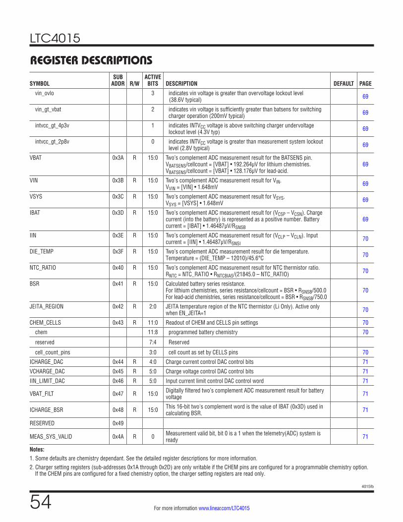
LTC4015
544015fb
For more information www.linear.com/LTC4015
SYMBOLSUB
ADDR R/WACTIVE
BITS DESCRIPTION DEFAULT PAGE
vin_ovlo 3 indicates vin voltage is greater than overvoltage lockout level (38.6V typical) 69
vin_gt_vbat 2 indicates vin voltage is sufficiently greater than batsens for switching charger operation (200mV typical) 69
intvcc_gt_4p3v 1 indicates INTVCC voltage is above switching charger undervoltage lockout level (4.3V typ) 69
intvcc_gt_2p8v 0 indicates INTVCC voltage is greater than measurement system lockout level (2.8V typical) 69
VBAT 0x3A R 15:0 Two’s complement ADC measurement result for the BATSENS pin. VBATSENS/cellcount = [VBAT] • 192.264µV for lithium chemistries. VBATSENS/cellcount = [VBAT] • 128.176µV for lead-acid.
69
VIN 0x3B R 15:0 Two’s complement ADC measurement result for VIN. VVIN = [VIN] • 1.648mV 69
VSYS 0x3C R 15:0 Two’s complement ADC measurement result for VSYS. VSYS = [VSYS] • 1.648mV 69
IBAT 0x3D R 15:0 Two’s complement ADC measurement result for (VCSP – VCSN). Charge current (into the battery) is represented as a positive number. Battery current = [IBAT] • 1.46487µV/RSNSB
69
IIN 0x3E R 15:0 Two’s complement ADC measurement result for (VCLP – VCLN). Input current = [IIN] • 1.46487µV/RSNSI
70
DIE_TEMP 0x3F R 15:0 Two’s complement ADC measurement result for die temperature. Temperature = (DIE_TEMP – 12010)/45.6°C 70
NTC_RATIO 0x40 R 15:0 Two’s complement ADC measurement result for NTC thermistor ratio. RNTC = NTC_RATIO • RNTCBIAS/(21845.0 – NTC_RATIO) 70
BSR 0x41 R 15:0 Calculated battery series resistance. For lithium chemistries, series resistance/cellcount = BSR • RSNSB/500.0 For lead-acid chemistries, series resistance/cellcount = BSR • RSNSB/750.0
70
JEITA_REGION 0x42 R 2:0 JEITA temperature region of the NTC thermistor (Li Only). Active only when EN_JEITA=1 70
CHEM_CELLS 0x43 R 11:0 Readout of CHEM and CELLS pin settings 70
chem 11:8 programmed battery chemistry 70
reserved 7:4 Reserved
cell_count_pins 3:0 cell count as set by CELLS pins 70
ICHARGE_DAC 0x44 R 4:0 Charge current control DAC control bits 71
VCHARGE_DAC 0x45 R 5:0 Charge voltage control DAC control bits 71
IIN_LIMIT_DAC 0x46 R 5:0 Input current limit control DAC control word 71
VBAT_FILT 0x47 R 15:0 Digitally filtered two’s complement ADC measurement result for battery voltage 71
ICHARGE_BSR 0x48 R 15:0 This 16-bit two's complement word is the value of IBAT (0x3D) used in calculating BSR. 71
RESERVED 0x49
MEAS_SYS_VALID 0x4A R 0 Measurement valid bit, bit 0 is a 1 when the telemetry(ADC) system is ready 71
Notes:1. Some defaults are chemistry dependant. See the detailed register descriptions for more information.2. Charger setting registers (sub-addresses 0x1A through 0x2D) are only writable if the CHEM pins are configured for a programmable chemistry option.
If the CHEM pins are configured for a fixed chemistry option, the charger setting registers are read only.
REGISTER DESCRIPTIONS

LTC4015
554015fb
For more information www.linear.com/LTC4015
DETAILED REGISTER DESCRIPTIONSVBAT_LO_ALERT_LIMIT (Sub-Address 0x01, Bits 15:0, R/W), VBAT_HI_ALERT_LIMIT (Sub-Address 0x02, Bits 15:0, R/W) These 16-bit words set upper and lower limits that can be used to trigger an SMBALERT based on the BATSENS pin voltage out of range. The values use the same two’s complement format as VBAT. For lithium chemistries, BATSENS/cellcount voltage HI/LO alert limit = [VBAT_xx_ALERT_LIMIT] • 192.264µV. For lead-acid batteries, BATSENS/cellcount voltage HI/LO alert limit = [VBAT_xx_ALERT_LIMIT] • 128.176µV
VIN_LO_ALERT_LIMIT (Sub-Address 0x03, Bits 15:0, R/W), VIN_HI_ALERT_LIMIT (Sub-Address 0x04, Bits 15:0, R/W) These 16-bit words set upper and lower limits that can be used to trigger an SMBALERT based on input voltage at the VIN pin out of range. The values use the same two’s complement format as VIN. Input voltage HI/LO alert limit = [VIN_xx_ALERT_LIMIT] • 1.648mV.
VSYS_LO_ALERT_LIMIT (Sub-Address 0x05, Bits 15:0, R/W), VSYS_HI_ALERT_LIMIT (Sub-Address 0x06, Bits 15:0, R/W) These 16-bit words set upper and lower limits that can be used to trigger an SMBALERT based on system voltage at the SYS pin out of range. The values use the same two’s complement format as VSYS. System voltage HI/LO alert limit = [VSYS_xx_ALERT_LIMIT] • 1.648mV.
IIN_HI_ALERT_LIMIT (Sub-Address 0x07, Bits 15:0, R/W) This 16-bit word sets an upper limit that can be used to trigger an SMBALERT based on input current above a certain value. IIN_HI_ALERT_LIMIT uses the same two’s complement format as IIN. Input current high alert limit = [IIN_HI_ALERT_LIMIT] • 1.46487µV/RSNSI.
IBAT_LO_ALERT_LIMIT (Sub-Address 0x08, Bits 15:0, R/W) This 16-bit word sets an upper limit that can be used to trigger an SMBALERT based on charge current below a certain value. IBAT_LO_ALERT_LIMIT uses the same two’s complement format as IBAT with battery discharge current being negative. Battery current low alert limit = [IBAT_LO_ALERT_LIMIT] • 1.46487µV/RSNSB.
DIE_TEMP_HI_ALERT_LIMIT (Sub-Address 0x09, Bits 15:0, R/W) This 16-bit word sets an upper limit that can be used to trigger an SMBALERT based on high die temperature. DIE_TEMP_HI_ALERT_LIMIT uses the same two’s complement format as DIE_TEMP. LTC4015 temperature = (DIE_TEMP – 12010)/45.6°C
BSR_HI_ALERT_LIMIT (Sub-Address 0x0A, Bits 15:0, R/W) This 16-bit word sets an upper limit that can be used to trigger an SMBALERT based on high battery series resistance. BSR_HI_ALERT_LIMIT uses the same format as BSR. The battery series resistance is a function of RSNSB, and can be computed as Ω/cellcount = [BSR/500] • RSNSB (lithium chemistries), or Ω/cellcount = [BSR/750] • RSNSB (lead-acid).
NTC_RATIO_HI_ALERT_LIMIT (Sub-Address 0x0B, Bits 15:0,R/W), NTC_RATIO_LO_ALERT_LIMIT (Sub-Address 0x0C, Bits 15:0, R/W) These 16-bit words set upper and lower limits that can be used to trigger an SMBALERT based on thermistor value out of range. The values use the same two’s complement format as NTC_RATIO. The thermistor value can be determined by the expression RNTC = RNTCBIAS • NTC_RATIO/(21,845 – NTC_RATIO). Recall that the thermistor has a negative temperature coefficient so higher temperatures correspond to lower NTC_RATIO readings and vice-versa. Thus, NTC_RATIO_HI_ALERT_LIMIT sets an upper alert limit for the value of NTC_RATIO which corresponds to a low (cold) temperature for the thermistor, and NTC_RATIO_LO_ALERT_LIMIT sets a lower alert limit for the value of NTC_RATIO which corresponds to a high (hot) temperature for the thermistor.

LTC4015
564015fb
For more information www.linear.com/LTC4015
DETAILED REGISTER DESCRIPTIONSEN_LIMIT_ALERTS (Sub-Address 0x0D, Bits 15:0, R/W) This register consists of individual limit alert enable bits. These bits enable monitoring and notification of limit excursions via SMBALERT and the LIMIT_ALERTS (0x36) register. See the section Programmable Alerts and Interrupt Controller for more information.
en_meas_sys_valid_alert (Sub-Address 0x0D, Bit 15, R/W) To achieve high measurement accuracy, the measurement system in the LTC4015 has a nominal warm up time of approximately 12ms. Setting this alert enable bit causes an SMBALERT when the measurement system indicates its results are valid. Note that the LTC4015 switching charger will not operate until the measurement system warm up period has passed, regardless of the state of en_meas_sys_valid_alert.
en_qcount_lo_alert (Sub-Address 0x0D, Bit 13, R/W) Setting this enable bit causes an SMBALERT when QCOUNT has fallen below QCOUNT_LO_ALERT_LIMIT. qcount_lo_alert is set to 1 by the LTC4015 if the alert occurs.
en_qcount_hi_alert (Sub-Address 0x0D, Bit 12, R/W) Setting this enable bit causes an SMBALERT when QCOUNT has exceeded QCOUNT_HI_ALERT_LIMIT. qcount_hi_alert is set to 1 by the LTC4015 if the alert occurs.
en_vbat_lo_alert (Sub-Address 0x0D, Bit 11, R/W) Setting this enable bit causes an SMBALERT when VBAT has fallen below VBAT_LO_ALERT_LIMIT. vbat_lo_alert is set to 1 by the LTC4015 if the alert occurs.
en_vbat_hi_alert (Sub-Address 0x0D, Bit 10, R/W) Setting this enable bit causes an SMBALERT when VBAT has exceeded VBAT_HI_ALERT_LIMIT. vbat_hi_alert is set to 1 by the LTC4015 if the alert occurs.
en_vin_lo_alert (Sub-Address 0x0D, Bit 9, R/W) Setting this enable bit causes an SMBALERT when VIN has fallen below VIN_LO_ALERT_LIMIT. vin_lo_alert is set to 1 by the LTC4015 if the alert occurs.
en_vin_hi_alert (Sub-Address 0x0D, Bit 8, R/W) Setting this enable bit causes an SMBALERT when VIN has exceeded VIN_HI_ALERT_LIMIT. vin_hi_alert is set to 1 by the LTC4015 if the alert occurs.
en_vsys_lo_alert (Sub-Address 0x0D, Bit 7, R/W) Setting this enable bit causes an SMBALERT when VSYS has fallen below VSYS_LO_ALERT_LIMIT. vsys_lo_alert is set to 1 by the LTC4015 if the alert occurs.
en_vsys_hi_alert (Sub-Address 0x0D, Bit 6, R/W) Setting this enable bit causes an SMBALERT when VSYS has exceeded VSYS_HI_ALERT_LIMIT. vsys_hi_alert is set to 1 by the LTC4015 if the alert occurs.
en_iin_hi_alert (Sub-Address 0x0D, Bit 5, R/W) Setting this enable bit causes an SMBALERT when IIN has exceeded IIN_HI_ALERT_LIMIT. iin_hi_alert is set to 1 by the LTC4015 if the alert occurs.

LTC4015
574015fb
For more information www.linear.com/LTC4015
DETAILED REGISTER DESCRIPTIONSen_ibat_lo_alert (Sub-Address 0x0D, Bit 4, R/W) Setting this enable bit causes an SMBALERT when IBAT has fallen below IBAT_LO_ALERT_LIMIT. ibat_lo_alert is set to 1 by the LTC4015 if the alert occurs.
en_die_temp_hi_alert (Sub-Address 0x0D, Bit 3, R/W) Setting this enable bit causes an SMBALERT when DIE_TEMP has exceeded DIE_TEMP_HI_ALERT_LIMIT. die_temp_hi_alert is set to 1 by the LTC4015 if the alert occurs.
en_bsr_hi_alert (Sub-Address 0x0D, Bit 2, R/W) Setting this enable bit causes an SMBALERT when BSR has exceeded BSR_HI_ALERT_LIMIT. bsr_hi_alert is set to 1 by the LTC4015 if the alert occurs.
en_ntc_ratio_hi_alert (Sub-Address 0x0D, Bit 1, R/W) Setting this enable bit causes an SMBALERT when NTC_RATIO has exceeded NTC_RATIO_HI_ALERT_LIMIT (cold battery). Recall that the thermistor has a negative temperature coefficient so higher temperatures correspond to lower NTC_RATIO readings and vice-versa. ntc_ratio_hi_alert is set to 1 by the LTC4015 if the alert occurs.
en_ntc_ratio_lo_alert (Sub-Address 0x0D, Bit 0, R/W) Setting this enable bit causes an SMBALERT when NTC_RATIO has fallen below NTC_RATIO_LO_ALERT_LIMIT (hot battery). Recall that the thermistor has a negative temperature coefficient so higher temperatures correspond to lower NTC_RATIO readings and vice-versa. ntc_ratio_lo_alert is set to 1 by the LTC4015 if the alert occurs.
EN_CHARGER_STATE_ALERTS (Sub-Address 0x0E, Bits 10:0, R/W) This register consists of individual charger state alert enable bits, which enable notification via SMBALERT based on the phase of a battery charge cycle. See the CHARGER_STATE (0x37) register details and the sections Battery Charger Algorithms and Programmable Alerts and Interrupt Controller for more information.
en_equalize_charge_alert (Sub-Address 0x0E, Bit 10, R/W) Setting this enable bit causes an SMBALERT when the LTC4015 is in the equalize phase of a battery charge cycle (equalize_charge=1, applies to lead-acid chemistries only).
en_absorb_charge_alert (Sub-Address 0x0E, Bit 9, R/W) Setting this enable bit causes an SMBALERT when the LTC4015 is in the absorb phase of a battery charge cycle (absorb_charge=1, applies to LiFePO4 and lead-acid chemistries only).
en_charger_suspended_alert (Sub-Address 0x0E, Bit 8, R/W) Setting this enable bit causes an SMBALERT when the LTC4015 charger is suspended (charger_suspended=1).
en_precharge_alert (Sub-Address 0x0E, Bit 7, R/W) Setting this enable bit causes an SMBALERT when the LTC4015 is in precondition charge phase of a battery charge cycle (precharge=1) due to the battery being below the low battery threshold of 2.9V/cell (applies to Li-Ion chem-istries only).
en_cc_cv_charge_alert (Sub-Address 0x0E, Bit 6, R/W) Setting this enable bit causes an SMBALERT when the LTC4015 is in the CC-CV phase of a battery charge cycle (cc_cv_charge=1).

LTC4015
584015fb
For more information www.linear.com/LTC4015
DETAILED REGISTER DESCRIPTIONSen_ntc_pause_alert (Sub-Address 0x0E, Bit 5, R/W) Setting this enable bit causes an SMBALERT when the LTC4015 is in thermistor pause state (ntc_pause=1) due to NTC_RATIO out of range as set by the JEITA_T1 and JEITA_T6 values. See the section J.E.I.T.A. Temperature Qualified Charging (applies to lithium chemistries only).
en_timer_term_alert (Sub-Address 0x0E, Bit 4, R/W) Setting this enable bit causes an SMBALERT when the LTC4015 is in timer termination state (timer_term=1) due to battery being at VCHARGE for more than MAX_CHARGE_TIME (applies to lithium chemistries only).
en_c_over_x_term_alert (Sub-Address 0x0E, Bit 3, R/W) Setting this enable bit causes an SMBALERT when the LTC4015 is in C/x termination state (c_over_x_term=1) due to IBAT dropping below C_OVER_X_THRESHOLD (applies to lithium chemistries only).
en_max_charge_time_fault_alert (Sub-Address 0x0E, Bit 2, R/W) Setting this enable bit causes an SMBALERT when the LTC4015 is in max charge time fault (max_charge_time_fault = 1) due to MAX_CHARGE_TIMER exceeding MAX_CHARGE_TIME during a charge cycle (applies to lithium chemistries only).
en_bat_missing_fault_alert (Sub-Address 0x0E, Bit 1, R/W) Setting this enable bit causes an SMBALERT if the LTC4015 is in battery missing fault state (bat_missing_fault=1) due to no battery detected.
en_bat_short_fault_alert (Sub-Address 0x0E, Bit 0, R/W) Setting this enable bit causes an SMBALERT if the LTC4015 is in shorted battery fault state (bat_short_fault=1) be-cause the battery was determined to be shorted during the battery detection phase at the beginning of a charge cycle.
EN_CHARGE_STATUS_ALERTS (Sub-Address 0x0F, Bits 3:0, R/W) This register consists of individual charge status alert enable bits, which enable notification via SMBALERT based on the status of the battery charge current control circuitry. See the CHARGE_STATUS register details and the section Programmable Alerts and Interrupt Controller for more information.
en_vin_uvcl_active_alert (Sub-Address 0x0F, Bit 3, R/W) Setting this enable bit causes an SMBALERT when the UVCL undervoltage current limit regulation loop of the LTC4015 is in control of the switching CHARGER current delivery (vin_uvcl_active=1).
en_iin_limit_active_alert (Sub-Address 0x0F, Bit 2, R/W) Setting this enable bit causes an SMBALERT when the input current regulation loop of the LTC4015 is in control of the switching CHARGER current delivery (iin_limit_active=1).
en_constant_current_alert (Sub-Address 0x0F, Bit 1, R/W) Setting this enable bit causes an SMBALERT when the battery charge current regulation loop of the LTC4015 is in control of the switching CHARGER current delivery (constant_current=1).
en_constant_voltage_alert (Sub-Address 0x0F, Bit 0, R/W) Setting this enable bit causes an SMBALERT when the battery voltage regulation loop of the LTC4015 is in control of the switching CHARGER current delivery (constant_voltage=1).

LTC4015
594015fb
For more information www.linear.com/LTC4015
DETAILED REGISTER DESCRIPTIONSQCOUNT_LO_ALERT_LIMIT (Sub-Address 0x10, Bits 15:0, R/W) QCOUNT_HI_ALERT_LIMIT (Sub-Address 0x11, Bits 15:0, R/W) These 16-bit words set and lower and upper limits on QCOUNT that can be used to trigger an SMBALERT when QCOUNT falls below QCOUNT_LO_ALERT_LIMIT, or QCOUNT exceeds QCOUNT_HI_ALERT_LIMIT. The values use the same format as QCOUNT.
QCOUNT_PRESCALE_FACTOR (Sub-Address 0x12, Bits 15:0, R/W) This 16-bit word along with RSNSB is used to set the qLSB value of Coulomb counter accumulator, QCOUNT.
qLSB =
QCOUNT_PRESCALE_FACTOR8333.33•RSNSB
A •s(COULOMBS)
QCOUNT (Sub-Address 0x13, Bits 15:0, R/W) This 16-bit word reports the current value of Coulomb counter accumulator, QCOUNT. This register can be written to represent a known state of charge of the battery.
qLSB =
QCOUNT_PRESCALE_FACTOR8333.33•RSNSB
A •s(COULOMBS)
CONFIG_BITS (Sub-Address 0x14, Bits 8:0, R/W)
This register consists of individual system configuration bits which control various features of the LTC4015.
suspend_charger (Sub-Address 0x14, Bit 8, R/W) Setting this bit causes battery charging to be suspended, and forces charger_suspended=1. A new battery charge cycle can be forced by setting and then resetting suspend_charger.
run_bsr (Sub-Address 0x14, Bit 5, R/W) Setting this bit causes a single battery series resistance (BSR) measurement to be made by the LTC4015. Once the series resistance measurement is complete, the LTC4015 resets the run_bsr bit to 0, and the result is reported as BSR. ICHARGE_BSR is the value of IBAT that was used in the BSR calculation. See the section Battery Series Resistance Measurement.
force_meas_sys_on (Sub-Address 0x14, Bit 4, R/W) Setting this bit causes the A/D measurement system to operate at all times, including when input power is unavailable (vin_gt_vbat=0). This feature is disabled by default in order to reduce battery-only load current. Setting this bit has the advantage of maintaining up-to-date system data, but will increase battery drain.
When input power is absent, the measurement system can be sampled periodically to reduce quiescent current. See the Measurement Subsystem description for details.
mppt_en_i2c (Sub-Address 0x14, Bit 3, R/W) Setting this bit causes the maximum power point tracking algorithm to run when the switching charger is active. The maximum power point algorithm uses the UVCL regulation loop to seek the optimum power point for resistive sources such as a solar panel. See the section maximum power point tracking for more information. The maximum power point algorithm can also be enabled by connecting the MPPT pin to the 2P5VCC pin. The mppt_en_i2c bit is logically ORed with the MPPT pin. To disable MPPT both the mppt_en_i2c bit and the MPPT pin must be low.
en_qcount (Sub-Address 0x14, Bit 2, R/W) Setting this bit enables the LTC4015 Coulomb counter. This feature is disabled by default to reduce quiescent current.

LTC4015
604015fb
For more information www.linear.com/LTC4015
DETAILED REGISTER DESCRIPTIONSIIN_LIMIT_SETTING (Sub-Address 0x15, Bits 5:0, R/W) These 6 bits control the target input current limit setting. The input current will be regulated to a maximum value given by (IIN_LIMIT_SETTING + 1) • 500µV/RSNSI.
VIN_UVCL_SETTING (Sub-Address 0x16, Bits 7:0, R/W) These 8 bits control the UVCLFB regulation loop servo voltage. The UVCLFB regulation voltage is given by (VIN_UVCL_SETTING + 1) • 4.6875mV. By default, this register is set to full-scale (0xFF), corresponding to 1.2V at UVCLFB pin. If enabled, the maximum power point tracking (MPPT) algorithm directly manipulates VIN_UVCL_SETTING.
ARM_SHIP_MODE (Sub-Address 0x19, Bits 15:0, R/W) Setting this register to 0x534D (ASCII for SM) arms LTC4015’s low power ship mode. The only allowed values for this register are 0x0000 and 0x534D, and once armed, ship mode cannot be disarmed (writing ARM_SHIP_MODE=0 does not disarm ship mode). Ship mode does not take effect until VIN drops below approximately 1V. See the section Low Power Ship Mode.
CHARGER SETTING REGISTER DESCRIPTIONS (Sub-Addresses 0x1A through 0x2E)
Registers which control the primary charging parameters, such as charge voltage and charge current are only writ-able when the CHEMn pins are configured for a programmable chemistry algorithm (Li-Ion-Prog, LiFePO4-Prog, or Lead-Acid-Prog). If the CHEMn pins are configured for a fixed chemistry algorithm (Li-Ion-Fixed-4.2, Li-Ion-Fixed-4.1, Li-Ion-fixed-4.0, LiFePO4-Fixed-3.6, LiFePO4-Fixed-3.8/3.6, or Lead-Acid-Fixed) the LTC4015 ignores writes to these registers. See the section Chemistry Selection for more information about configuring the CHEMn pins.
ICHARGE_TARGET (Sub-Address 0x1A, bits 4:0, Fixed: R, Programmable: R/W) This register controls the target charge current regulation servo level for lead-acid batteries or if en_jeita=0 for lithium chemistries. For lithium chemistries, if en_jeita=1 (default) ICHARGE_TARGET is controlled by ICHARGE_JEITA_n (see the section JEITA Temperature Controlled Charging). The charge current regulation servo level is generally given by (ICHARGE_TARGET + 1) × 1mV/RSNSB, except during Li-Ion precondition charge phase when the charge current regulation servo level is reduced by approximately a factor of 10 (rounded down to an increment of 1mV/RSNSB).
VCHARGE_SETTING (Sub-Address 0x1B, bits 5:0, Fixed: R, Programmable: R/W) This register controls the charge voltage regulation servo level. The LTC4015 does not monitor or balance individual cells – the full battery stack voltage is divided by number of cells (V/cell) for simplicity only. The 4015 is not a substitute for pack protection!
For Li-Ion batteries, only the lower five bits (4:0) are active, and the charge voltage level is given by (VCHARGE_SETTING/80.0 + 3.8125)V/cell. If en_jeita=1, VCHARGE_SETTING is controlled by vcharge_jeita_n (see the section JEITA Temperature Qualified Charging). To maintain inherent over charge protection, the maximum Li-Ion charge voltage level is 4.2V/cell.
For LiFePO4 batteries, only the lower five bits (4:0) are active, and the charge voltage level is given by (VCHARGE_SETTING/80.0 + 3.4125)V/cell. If en_jeita=1, VCHARGE_SETTING is controlled by vcharge_jeita_n (see the section JEITA Temperature Qualified Charging). To maintain inherent over-charge protection, the maximum LiFePO4 charge voltage level is 3.8V/cell.
For lead-acid batteries, if en_lead_acid_temp_comp=1, the charge voltage level is given by (VCHARGE_SETTING/105.0 + 2.0)V/cell at 25°C when a thermistor with a β value of 3490k is used. See the section Lead-Acid Temperature Compensated Charging for more information. If en_lead_acid_temp_comp=1, the value of VCHARGE_SETTING is limited to a maximum setting of 35, which corresponds to 2.333V/cell. If en_lead_acid_temp_comp=0, the charge

LTC4015
614015fb
For more information www.linear.com/LTC4015
DETAILED REGISTER DESCRIPTIONSvoltage level is given by (VCHARGE_SETTING/105.0 + 2.0)V/cell, regardless of temperature. To maintain inherent over charge protection, the maximum lead-acid charge voltage level is 2.6 V/cell.
VABSORB_DELTA (Sub-Address 0x2A, bits 5:0, Fixed: R, Programmable: R/W) This register controls the absorb adder voltage for LiFePO4 and lead-acid batteries in absorb charge phase. The absorb charge phase battery voltage servo level is based on the sum of the absorb adder voltage and the charge voltage level.
For Li-Ion batteries, VABSORB_DELTA is ignored.
For LiFePO4 batteries, only the lower five bits (4:0) are active, and the absorb voltage level is given by (VABSORB_DELTA + VCHARGE_SETTING)/80 + 3.4125 V/cell, limited to a maximum of 3.8 V/cell. Setting VABSORB_DELTA=0 disables the absorb phase. See the section LiFePO4 Absorb Charge for more information.
For lead-acid batteries, if en_lead_acid_temp_comp=1, the absorb voltage level is given by (VABSORB_DELTA + VCHARGE_SETTING)/105.0 + 2.0V/cell at 25°C when a thermistor with a β value of 3490k is used. See the section Lead-Acid Temperature Compensated Charging for more information. If en_lead_acid_temp_comp=0, the absorb voltage level is given by (VABSORB_DELTA + VCHARGE_SETTING)/105.0 + 2.0V/cell, regardless of temperature. To maintain inherent over charge protection, the maximum lead-acid absorb voltage level is 2.6 V/cell.
VEQUALIZE_DELTA (Sub-Address 0x2C, Bits 5:0, Fixed: R, Programmable: R/W) These six bits control the equalize adder voltage for lead-acid batteries in equalize charge phase. The equalize charge phase battery voltage servo level is based on the sum of the equalize adder voltage and the vcharge level.
For lead-acid batteries, if en_lead_acid_temp_comp=1, the equalize voltage level is given by (VEQUALIZE_DELTA + VCHARGE_SETTING) / 105.0 + 2.0 V/cell at 25°C when a typical curve two thermistor is used. See the section Lead-Acid Temperature Compensated Charging for more information. If en_lead_acid_temp_comp=0, the equalize voltage level is given by ((VEQUALIZE_DELTA + VCHARGE_SETTING)/105.0 + 2.0)V/cell, regardless of temperature. To maintain inherent over charge protection, the maximum lead-acid equalize voltage level is 2.6V/cell.
For lithium chemistries, VEQUALIZE_DELTA is ignored.
C_OVER_X_THRESHOLD (Sub-Address 0x1C, Bits 15:0, Fixed: R, Programmable: R/W) This 16-bit word sets the IBAT value used to qualify C/x detection for charge phase termination/transition. C_OVER_X_THRESHOLD uses the same format as IBAT, and the C/x current level is given by C_OVER_X_THRESHOLD/(RSNSB • 21845.0/0.032V). The default value for C_OVER_X_THRESHOLD is 2184, which corresponds to 10% (3.2mV) of a 32mV/ RSNSB full-scale charge current. C/x detection is disabled if C_OVER_X_THRESHOLD is set to zero.
For Li-Ion batteries, if en_c_over_x_term=1 (0 by default), C/x charge termination occurs after the battery reaches the charge voltage level and IBAT drops below C_OVER_X_THRESHOLD. See the section C/x Termination.
For LiFePO4 batteries, if en_c_over_x_term=1 (0 by default), C/x charge termination occurs after the battery reaches vcharge level and IBAT drops below C_OVER_X_THRESHOLD during CC-CV charge phase. See the section C/x Termination. If the optional LiFePO4 absorb charge phase is employed and if C_OVER_X_THRESHOLD is set to a non-zero value, the absorb phase ends if the battery voltage reaches absorb level and IBAT drops below C_OVER_X_THRESHOLD, and CC-CV phase begins. See the section LiFePO4 Absorb Charge.
For lead-acid batteries, if C_OVER_X_THRESHOLD is non-zero, absorb charge phase ends after the battery voltage reaches absorb level and IBAT drops below C_OVER_X_THRESHOLD, and the CC-CV charge phase continues indefinitely.

LTC4015
624015fb
For more information www.linear.com/LTC4015
DETAILED REGISTER DESCRIPTIONSMAX_CV_TIME (Sub-Address 0x1D, Bits 15:0, Fixed: R, Programmable: R/W) For lithium chemistries, this 16-bit word sets the termination time limit at one second per count. If the charger is in the CV state for MAX_CV_TIME seconds, timer termination occurs. The actual timer value is reported in CV_TIMER. See the section Timer Termination for more information. The default setting is four hours (14,400) for Li- Ion batteries and one hour (3,600) for LiFePO4 batteries. For lead-acid batteries, MAX_CV_TIME is ignored.
MAX_ABSORB_TIME (Sub-Address 0x2B, Bits 15:0, Fixed: R, Programmable: R/W) For LiFePO4 and lead-acid batteries, this 16-bit word sets an upper limit on the time (at one second per count) that the battery can be in the absorb charge phase. The actual timer value is reported in ABSORB_TIMER. See the sections LiFePO4 Absorb Charge and Lead-Acid Absorb Charge. For Li-Ion batteries, MAX_ABSORB_TIME is ignored.
EQUALIZE_TIME (Sub-Address 0x2D, Bits 15:0, Fixed: R, Programmable: R/W) For lead-acid batteries, this 16-bit word sets the time (at one second per count) for the equalization charge phase. For lead-acid batteries, the default setting is 3600 seconds. See the section Lead-Acid Equalization Charge. For lithium chemistries, EQUALIZE_TIME is ignored.
MAX_CHARGE_TIME (Sub-Address 0x1E, Bits 15:0, Fixed: R, Programmable: R/W) For lithium chemistries, this 16-bit word sets the max_charge_time fault detection time at one second per count. The default setting is 18.2 hours (65535). If the MAX_CHARGE_TIMER exceeds MAX_CHARGE_TIME during charging, a max charge time fault occurs. See the section Max Charge Time Fault for more information. For lead-acid batteries, MAX_CHARGE_TIME is ignored.
LIFEP04_RECHARGE_THRESHOLD (Sub-Address 0x2E, Bits 15:0, Fixed: R, Programmable: R/W) In LiFePO4 programmable mode only, this 16 bit two's complement word sets the recharge threshold, where the recharge threshold/cell = [LiFePO4_RECHARGE_THRESHOLD] • 192.264µV. Default is 0x4410 which is 3.35V/cell.
JEITA_Tn (Sub-Address 0x1F Through 0x24, Bits 15:0, Fixed: R, Programmable: R/W) (n = 1,2,3,4,5,6) For lithium chemistries, these six 16-bit words set the JEITA temperature region break points T1 – T6, and have the same format as NTC_RATIO. The temperatures are based on the thermistor reading from the measurement system. Recall that the thermistor has a negative temperature coefficient so JEITA_T1, representing colder temperatures, will have the highest value and JEITA_T6, representing warmer temperatures, will have the lowest value. See the section JEITA Temperature Qualified Charging. JEITA_Tn are ignored for lead-acid batteries or if en_jeita=0.
Programming of JEITA ValuesREGION 1 REGION 2 REGION 3 REGION 4 REGION 5 REGION 6 REGION 7
[JEITA_T1] [JEITA_T2] [JEITA_T3 ] [JEITA_T4] [JEITA_T5] [JEITA_T6]
CHARGER OFF
icharge_jeita_2 icharge_jeita_3 icharge_jeita_4 icharge_jeita_5 icharge_jeita_6 CHARGER OFFvcharge_jeita_2 vcharge_jeita_3 vcharge_jeita_4 vcharge_jeita_5 vcharge_jeita_6
VCHARGE_JEITA_6_5 (Sub-Address 0x25, Bits 9:0, Fixed: R, Programmable: R/W), VCHARGE_JEITA_4_3_2 (Sub-Address 0x26, Bits 14:0, Fixed: R, Programmable: R/W) For lithium chemistries, these two registers contain the charge voltage settings to be used in the JEITA voltage vs temperature profile. VCHARGE_JEITA_6_5 contains two bit packed values, vcharge_jeita_6 (bits 9:5) and vcharge_jeita_5

LTC4015
634015fb
For more information www.linear.com/LTC4015
DETAILED REGISTER DESCRIPTIONS(bits 4:0). VCHARGE_JEITA_4_3_2 contains three bit packed values, vcharge_jeita_4 (bits 14:10), vcharge_jeita_3 (bits 9:5), and vcharge_jeita_2 (bits 4:0). These registers are ignored for lead-acid batteries or if en_jeita=0.
vcharge_jeita_n (n = 2,3,4,5,6) These five 5-bit values set the VCHARGE_SETTING values to be used in each of the JEITA voltage vs temperature regions. There are no defined charge voltages for regions 1 and 7 because battery charging is paused in these regions. See the JEITA Temperature Qualified Charging section.
Programming of JEITA ValuesREGION 1 REGION 2 REGION 3 REGION 4 REGION 5 REGION 6 REGION 7
[JEITA_T1] [JEITA_T2] [JEITA_T3 ] [JEITA_T4] [JEITA_T5] [JEITA_T6]
CHARGER OFF
icharge_jeita_2 icharge_jeita_3 icharge_jeita_4 icharge_jeita_5 icharge_jeita_6 CHARGER OFFvcharge_jeita_2 vcharge_jeita_3 vcharge_jeita_4 vcharge_jeita_5 vcharge_jeita_6
ICHARGE_JEITA_6_5 (Sub-Address 0x27, Bits 9:0, Fixed: R, Programmable: R/W), ICHARGE_JEITA_4_3_2 (Sub-Address 0x28, Bits 14:0, Fixed: R, Programmable: R/W) For lithium chemistries, these two registers contain the charge current settings to be used in the JEITA current vs temperature profile. ICHARGE_JEITA_6_5 contains two bit packed values, icharge_jeita_6 (bits 9:5) and icharge_jeita_5 (bits 4:0). ICHARGE_JEITA_4_3_2 contains three bit packed values, icharge_jeita_4 (bits 14:10), icharge_jeita_3 (bits 9:5), and icharge_jeita_2 (bits 4:0). These registers are ignored for lead-acid batteries or if en_jeita=0.
icharge_jeita_n (n = 2,3,4,5,6) These five 5-bit values set the ICHARGE_TARGET values to be used in each of the JEITA current vs temperature regions. There are no defined charge currents for regions 1 and 7 because battery charging is paused in these regions. See the JEITA Temperature Qualified Charging section.
Programming of JEITA ValuesREGION 1 REGION 2 REGION 3 REGION 4 REGION 5 REGION 6 REGION 7
[JEITA_T1] [JEITA_T2] [JEITA_T3 ] [JEITA_T4] [JEITA_T5] [JEITA_T6]
CHARGER OFF
icharge_jeita_2 icharge_jeita_3 icharge_jeita_4 icharge_jeita_5 icharge_jeita_6 CHARGER OFFvcharge_jeita_2 vcharge_jeita_3 vcharge_jeita_4 vcharge_jeita_5 vcharge_jeita_6
CHARGER_CONFIG_BITS (Sub-Address 0x29, Bits 2:0, Fixed: R, Programmable: R/W)
This register consists of individual battery charger configuration bits which enable specific battery charger functions.
en_c_over_x_term (Sub-Address 0x29, Bit 2, Fixed: R, Programmable: R/W) For lithium chemistries, setting this bit enables C/x charge termination, in conjunction with C_OVER_X_THRESHOLD. For lead-acid batteries, en_c_over_x_term is ignored. Default is 0.
en_lead_acid_temp_comp (Sub-Address 0x29, Bit 1, Fixed: R, Programmable: R/W) For lead-acid batteries, setting this bit enables temperature compensated charge voltage levels as detailed in the Lead-Acid Temperature Compensated Charging section. Default is 1 for lead-acid batteries. For lithium chemistries, en_lead_acid_temp_comp is ignored.
en_jeita (Sub-Address 0x29, Bit 0, Fixed: R, Programmable: R/W) For lithium chemistries, setting this bit enables the JEITA temperature qualified algorithm as detailed in the JEITA Temperature Qualified Charging section. The charging parameters are set by JEITA_Tn, vcharge_jeita_n, and icharge_jeita _n. Default is 1 for lithium chemistries. For lead-acid batteries, en_jeita is ignored.

LTC4015
644015fb
For more information www.linear.com/LTC4015
DETAILED REGISTER DESCRIPTIONSREADOUTS, STATUS, AND ALERTS (Sub-Addresses 0x34 through 0x46)
MAX_CHARGE_TIMER (Sub-Address 0x30, Bits 15:0, R) For lithium chemistries, this 16-bit word indicates the time (in seconds) that the battery has been charging. See the MAX_CHARGE_TIME register description and the section Maximum Charge Time for more information. For lead-acid batteries, MAX_CHARGE_TIMER is not used.
CV_TIMER (Sub-Address 0x31, Bits 10:0, R) For lithium chemistries, this 16-bit word indicates the time (in seconds) that the battery has been in constant-voltage regulation. See the MAX_CV_TIME register description and the section Timer Termination for more information. For lead-acid batteries, CV_TIMER is not used.
ABSORB_TIMER (Sub-Address 0x32, Bits 10:0, R) For LiFePO4 and lead-acid batteries, this 16-bit word indicates the time (in seconds) that the battery has been in absorb phase. See the MAX_ABSORB_TIME register description and the sections LiFePO4 Absorb Charge and Lead-Acid Absorb Charge for more information. For Li-Ion batteries, ABSORB_TIMER is not used.
EQUALIZE_TIMER (Sub-Address 0x33, Bits 15:0, Fixed: R, Programmable: R/W) For lead-acid batteries, this 16-bit word indicates the time (in seconds) that the battery has been in equalization charge phase. See the EQUALIZE_TIME register description and the section Lead-Acid Equalization Charge. For lithium chemistries, EQUALIZE_TIMER is not used.
CHARGER_STATE (Sub-Address 0x34, Bits 10:0, R) This register consists of individual battery charger state indicator bits. Individual bits are mutually exclusive (a maximum of one bit is asserted at any given time). See the section Battery Charger Algorithms for more information regarding the charger states.
equalize_charge (Sub-Address 0x34, Bit 10, R) This bit indicates that the LTC4015 is in the equalize phase of a battery charge cycle (applies to lead-acid chemis-tries only).
absorb_charge (Sub-Address 0x34, Bit 9, R) This bit indicates that the LTC4015 is in the absorb phase of a battery charge cycle (applies to LiFePO4 and lead-acid chemistries only).
charger_suspended (Sub-Address 0x34, Bit 8, R) This bit indicates that the LTC4015 charger is suspended, due to any of the following conditions occurring: (a) the input voltage on the VIN pin falls below or within 100mV of the BATSENS pin voltage, (b) suspend_charger is writ-ten to 1 via the serial port, or (c) a system fault condition occurs (VIN overvoltage, 2P5VCC undervoltage, INTVCC undervoltage, DRVCC undervoltage, thermal shutdown, missing RT resistor, or invalid combination of CELLS pins).
precharge (Sub-Address 0x34, Bit 7, R) This bit indicates that the LTC4015 is in the precondition charge phase of a battery charge cycle due to the battery being below the low battery threshold of 2.9V/cell (applies to Li-Ion chemistries only).
cc_cv_charge (Sub-Address 0x34, Bit 6, R) This bit indicates that the LTC4015 is in the CC-CV phase of a battery charge cycle.

LTC4015
654015fb
For more information www.linear.com/LTC4015
DETAILED REGISTER DESCRIPTIONSntc_pause (Sub-Address 0x34, Bit 5, R) This bit indicates that the LTC4015 is in thermistor pause state due to NTC_RATIO out of range as set by the JEITA_Tn values. See the section JEITA Temperature Qualified Charging (applies to lithium chemistries only).
timer_term (Sub-Address 0x34, Bit 4, R) This bit indicates that the LTC4015 is in timer termination state due to battery being at the vcharge voltage for more than MAX_CV_TIME (applies to lithium chemistries only).
c_over_x_term (Sub-Address 0x34, Bit 3, R) This bit indicates that the LTC4015 is in C/x termination state due to IBAT dropping below C_OVER_X_THRESHOLD (applies to lithium chemistries only).
max_charge_time_fault (Sub-Address 0x34, Bit 2, R) This bit indicates that the LTC4015 is in max charge time fault state due to MAX_CHARGE_TIMER exceeding MAX_CHARGE_TIME during a charge cycle (applies to lithium chemistries only).
bat_missing_fault (Sub-Address 0x34, Bit 1, R) This bit indicates that the LTC4015 is in battery missing fault state due to no battery detected.
bat_short_fault (Sub-Address 0x34, Bit 0, R) This bit indicates that the LTC4015 is in battery short fault state due to a shorted battery detected.
CHARGE_STATUS (Sub-Address 0x35, Bits 3:0, R) This register consists of individual status bits which indicate status of the battery charge current control circuitry. Individual bits are mutually exclusive (a maximum of one bit is asserted at any given time).
vin_uvcl_active (Sub-Address 0x35, Bit 3, R) This bit indicates that the UVCLFB pin of the undervoltage current limit loop of the LTC4015 is in control of the switching charger current delivery based on VIN_UVCL_SETTING.
iin_limit_active (Sub-Address 0x35, Bit 2, R) This bit indicates that the input current regulation loop of the LTC4015 is in control of the switching charger current delivery based on IIN_LIMIT_SETTING.
constant_current (Sub-Address 0x35, Bit 1, R) This bit indicates that the battery charge current regulation loop of the LTC4015 is in control of the switching charger current delivery based on ICHARGE_DAC.
constant_voltage (Sub-Address 0x35, Bit 0, R) This bit indicates that the battery voltage regulation loop of the LTC4015 is in control of the switching charger current delivery based on VCHARGE_DAC.
LIMIT_ALERTS (Sub-Address 0x36, Bits 15:0, R/Clear) This register consists of individual alert bits which can optionally indicate that limit excursions have caused an SMBALERT to occur. The LTC4015 checks for new limits excursions at the end of every A/D measurement system cycle (approximately 6.5ms), and LIMIT_ALERTS is updated accordingly. Individual alert bits are enabled by EN_LIMIT_ALERTS.
Once asserted, alert bits remain high until disabled or cleared. Writing a 0 to any bit clears that alert. If an enabled alert is cleared and the alerting condition remains, a new alert is triggered immediately. When a new alert occurs, the LTC4015 pulls down the SMBALERT pin and holds it low until it completes a response to an alert response algorithm

LTC4015
664015fb
For more information www.linear.com/LTC4015
DETAILED REGISTER DESCRIPTIONS(ARA). See the section Programmable Alerts and Interrupt Controller for more information regarding the SMBALERT and ARA functions.
meas_sys_valid_alert (Sub-Address 0x36, Bit 15, R/Clear) To achieve high measurement accuracy, the measurement system in the LTC4015 has a typical warm up time of approximately 12ms. If en_meas_sys_valid_alert=1, the meas_sys_valid_alert bit indicates that an SMBALERT has occurred because the warm-up period has passed and the A/D measurement system results are valid. This can be particularly useful in battery only mode for periodic sampling of the measurement system; see force_meas_sys_on for more information.
qcount_lo_alert (Sub-Address 0x36, Bit 13, R/Clear) If en_qcount_lo_alert=1, this bit indicates that an SMBALERT has occurred because QCOUNT has fallen below QCOUNT_LO_ALERT_LIMIT.
qcount_hi_alert (Sub-Address 0x36, Bit 12, R/Clear) If en_qcount_hi_alert=1, this bit indicates that an SMBALERT has occurred because QCOUNT has exceeded QCOUNT_HI_ALERT_LIMIT.
vbat_lo_alert (Sub-Address 0x36, Bit 11, R/Clear) If en_vbat_lo_alert =1, this bit indicates that an SMBALERT has occurred because VBAT has fallen below VBAT_LO_ALERT_LIMIT.
vbat_hi_alert (Sub-Address 0x36, Bit 10, R/Clear) If en_vbat_hi_alert =1, this bit indicates that an SMBALERT has occurred because VBAT has exceeded VBAT_HI_ALERT_LIMIT.
vin_lo_alert (Sub-Address 0x36, Bit 9, R/Clear) If en_vin_lo_alert =1, this bit indicates that an SMBALERT has occurred because VIN has fallen below VIN_LO_ALERT_LIMIT.
vin_hi_alert (Sub-Address 0x36, Bit 8, R/Clear) If en_vin_hi_alert =1, this bit indicates that an SMBALERT has occurred because VIN has exceeded VIN_HI_ALERT_LIMIT.
vsys_lo_alert (Sub-Address 0x36, Bit 7, R/Clear) If en_vsys_lo_alert =1, this bit indicates that an SMBALERT has occurred because VSYS has fallen below VSYS_LO_ALERT_LIMIT.
vsys_hi_alert (Sub-Address 0x36, Bit 6, R/Clear) If en_vsys_hi_alert =1, this bit indicates that an SMBALERT has occurred because VSYS has exceeded VSYS_HI_ALERT_LIMIT.
iin_hi_alert (Sub-Address 0x36, Bit 5, R/Clear) If en_iin_hi_alert =1, this bit indicates that an SMBALERT has occurred because IIN has exceeded IIN_HI_ALERT_LIMIT.
ibat_lo_alert (Sub-Address 0x36, Bit 4, R/Clear) If en_ibat_lo_alert =1, this bit indicates that an SMBALERT has occurred because IBAT has fallen below IBAT_LO_ALERT_LIMIT.

LTC4015
674015fb
For more information www.linear.com/LTC4015
DETAILED REGISTER DESCRIPTIONSdie_temp_hi_alert (Sub-Address 0x36, Bit 3, R/Clear) If en_die_temp_hi_alert =1, this bit indicates that an SMBALERT has occurred because DIE_TEMP has exceeded DIE_TEMP_HI_ALERT_LIMIT.
bsr_hi_alert (Sub-Address 0x36, Bit 2, R/Clear) If en_bsr_hi_alert =1, this bit indicates that an SMBALERT has occurred because BSR has exceeded BSR_HI_ALERT_LIMIT.
ntc_ratio_hi_alert (Sub-Address 0x36, Bit 1, R/Clear) If en_ntc_ratio_hi_alert =1, this bit indicates that an SMBALERT has occurred because NTC_RATIO has exceeded NTC_RATIO_HI_ALERT_LIMIT (cold battery).
ntc_ratio_lo_alert (Sub-Address 0x36, Bit 0, R/Clear) If en_ntc_ratio_hi_alert =1, this bit indicates that an SMBALERT has occurred because NTC_RATIO has fallen below NTC_RATIO_LO_ALERT_LIMIT (hot battery)
CHARGER_STATE_ALERTS (Sub-Address 0x37, Bits 10:0, R/Clear) This register consists of individual battery charger state alert bits. Individual alert bits will be asserted if the individual alert has been enabled and the transition into that state occurs.
Once asserted, alert bits remain high until disabled or cleared. Writing a 0 to any bit clears that alert. If an enabled alert is cleared and the alerting condition remains, a new alert is triggered immediately. When a new alert occurs, the LTC4015 pulls down the SMBALERT pin and holds it low until an alert response algorithm (ARA) is completed. See the section Programmable Alerts and Interrupt Controller for more information regarding the SMBALERT and ARA functions.
equalize_charge_alert (Sub-Address 0x37, Bit 10, R/Clear) If en_equalize_charge_alert=1, this bit indicates that an SMBALERT has occurred due to the occurrence of equalize_charge (applies to lead-acid chemistries only).
absorb_charge_alert (Sub-Address 0x37, Bit 9, R/Clear) If en_absorb_charge_alert=1, this bit indicates that an SMBALERT has occurred due to the occurrence of absorb_charge (applies to LiFePO4 and lead-acid chemistries only).
charger_suspended_alert (Sub-Address 0x37, Bit 8, R/Clear) If en_charger_suspended_alert=1, this bit indicates that an SMBALERT has occurred due to the occurrence of charger_suspended.
precharge_alert (Sub-Address 0x37, Bit 7, R/Clear) If en_precharge _alert=1, this bit indicates that an SMBALERT has occurred due to the occurrence of precharge.
cc_cv_charge_alert (Sub-Address 0x37, Bit 6, R/Clear) If en_cc_cv_charge _alert=1, this bit indicates that an SMBALERT has occurred due to the occurrence of cc_cv_charge.
ntc_pause_alert (Sub-Address 0x37, Bit 5, R/Clear) If en_ntc_pause_alert=1, this bit indicates that an SMBALERT has occurred due to the occurrence of ntc_pause.
timer_term_alert (Sub-Address 0x37, Bit 4, R/Clear) If en_timer_term_alert=1, this bit indicates that an SMBALERT has occurred due to the occurrence of timer_term.
c_over_x_term_alert (Sub-Address 0x37, Bit 3, R/Clear) If en_c_over_x_term_alert=1, this bit indicates that an SMBALERT has occurred due to the occurrence of c_over_x_term.

LTC4015
684015fb
For more information www.linear.com/LTC4015
DETAILED REGISTER DESCRIPTIONSmax_charge_time_fault_alert (Sub-Address 0x37, Bit 2, R/Clear) If en_max_charge_time_fault_alert=1, this bit indicates that an SMBALERT has occurred due to the occurrence of a max_charge_time_fault.
bat_missing_fault_alert (Sub-Address 0x37, Bit 1, R/Clear) If en_bat_missing_fault_alert=1, this bit indicates that an SMBALERT has occurred due to the occurrence of bat_missing_fault.
bat_short_fault_alert (Sub-Address 0x37, Bit 0, R/Clear) If en_bat_short_fault_alert=1, this bit indicates that an SMBALERT has occurred due to the occurrence of bat_short_fault.
CHARGE_STATUS_ALERTS (Sub-Address 0x38, Bits 3:0, R/Clear) This register consists of individual battery charger charge status alert bits. Individual alert bits will be asserted if the individual alert has been enabled and the transition into that state occurs.
Once asserted, alert bits remain high until disabled or cleared. Writing a 0 to any bit clears that alert. If an enabled alert is cleared and the alerting condition remains, a new alert is triggered immediately. When a new alert occurs, the LTC4015 pulls down the SMBALERT pin and holds it low until an alert response algorithm (ARA) is completed. See the section Programmable Alerts and Interrupt Controller for more information regarding the SMBALERT and ARA functions.
vin_uvcl_active_alert (Sub-Address 0x38, Bit 3, R/Clear) If en_vin_uvcl_active_alert=1, this bit indicates that an SMBALERT has occurred because the UVCL undervolt-age current limit regulation loop of the LTC4015 has taken control of the switching regulator charger delivery (vin_uvcl_active=1).
iin_limit_active_alert (Sub-Address 0x38, Bit 2, R/Clear) If en_iin_limit_active_alert=1, this bit indicates that an SMBALERT has occurred because the input current regulation loop of the LTC4015 has taken control of the switching regulator charger delivery (iin_limit_active=1).
constant_current_alert (Sub-Address 0x38, Bit 1, R/Clear) If en_constant_current_alert=1, this bit indicates that an SMBALERT has occurred because the battery charge current regulation loop of the LTC4015 has taken control of the switching charger current delivery (constant_current=1).
constant_voltage_alert (Sub-Address 0x38, Bit 0, R/Clear) If en_constant_voltage_alert=1, this bit indicates that an SMBALERT has occurred because the battery voltage regulation loop of the LTC4015 has taken control of the switching charger current delivery (constant_voltage=1).
SYSTEM_STATUS (Sub-Address 0x39, Bits 13:0, R)
This register consists of individual real-time status bits which indicate various system conditions.
charger_enabled (Sub-Address 0x39, Bit 13, R) This bit indicates that the LTC4015 is actively charging a battery.
mppt_en_pin (Sub-Address 0x39, Bit 11, R) This bit indicates that the external MPPT pin is detected as being high and maximum power point tracking is enabled.
equalize_req (Sub-Address 0x39, Bit 10, R) This bit indicates that a rising edge has been detected at the EQ pin and a lead-acid equalization charge is running or is queued to run. See Lead-Acid Equalization Charge.

LTC4015
694015fb
For more information www.linear.com/LTC4015
DETAILED REGISTER DESCRIPTIONSdrvcc_good (Sub-Address 0x39, Bit 9, R) This bit indicates that the DRVCC pin voltage is above the DRVCC undervoltage lockout level (4.3V typical).
cell_count_error (Sub-Address 0x39, Bit 8, R) This bit indicates that an invalid combination of CELLS pin settings have been detected.
ok_to_charge (Sub-Address 0x39, Bit 6, R) This bit indicates that all system conditions are met to allow battery charging operation.
no_rt (Sub-Address 0x39, Bit 5, R) This bit indicates that no frequency setting resistor is detected on the RT pin. The RT pin impedance detection circuit will typically indicate a missing RT resistor for values above 1.4MΩ.
thermal_shutdown (Sub-address 0x39, Bit 4, R) This bit indicates that the LTC4015 is in thermal shutdown protection due to an excessively high die temperature (typically 160°C and above).
vin_ovlo (Sub-address 0x39, Bit 3, R) This bit indicates that the LTC4015 is in input voltage shutdown protection due to an input voltage above its protec-tion shutdown threshold of approximately 38.6V (typical).
vin_gt_vbat (Sub-Address 0x39, Bit 2, R) This bit indicates that the VIN pin input voltage is sufficiently above the BATSENS battery voltage to allow charging operation (typically +200mV).
intvcc_gt_4p3v (Sub-Address 0x39, Bit 1, R) This bit indicates that the INTVCC voltage is above the switching charger undervoltage lockout threshold value of 4.3V (typical).
intvcc_gt2p8v (Sub-Address 0x39, Bit 0, R) This bit indicates that the INTVCC pin voltage is above the measurement system undervoltage lockout threshold value of 2.8V (typical).
VBAT (Sub-Address 0x3A, Bits 15:0, R) This 16-bit two’s complement word indicates the A/D measurement result for the BATSENS pin. VBATSENS/cellcount = [VBAT] • 192.264µV for lithium chemistries. VBATSENS/cellcount = [VBAT] • 128.176µV for lead-acid.
VIN (Sub-Address 0x3B, Bits 15:0, R) This 16-bit two’s complement word indicates the A/D measurement result for the VIN pin voltage divided by 30. Input voltage, VVIN = [VIN] • 1.648mV
VSYS (Sub-Address 0x3C, Bits 15:0, R) This 16-bit two’s complement word indicates the A/D measurement result for the SYS pin voltage divided by 30. System voltage, VSYS = [VSYS] • 1.648mV
IBAT (Sub-Address 0x3D, Bits 15:0, R) This 16-bit word indicates the A/D measurement of 37.5 • (VCSP – VCSN) at the CSP, CSN pins. Negative values are represented in two’s complement notation and indicate current flowing out of (discharging) the battery. Battery current = [IBAT] • 1.46487µV/RSNSB

LTC4015
704015fb
For more information www.linear.com/LTC4015
DETAILED REGISTER DESCRIPTIONSIIN (Sub-Address 0x3E, Bits 15:0, R) This 16-bit word indicates the A/D measurement of 37.5 • (VCLP – VCLN) at the CLP, CLN pins. Input current = [IIN] • 1.46487µV/RSNSI
DIE_TEMP (Sub-Address 0x3F, Bits 15:0, R) This 16-bit two’s complement word indicates the A/D measurement result for LTC4015 die temperature. LTC4015 temperature = (DIE_TEMP – 12010)/45.6°C
NTC_RATIO (Sub-Address 0x40, Bits 15:0, R) This 16-bit two’s complement word indicates the A/D measurement result for RNTC/(RNTC + RNTCBIAS). The thermistor value can be determined by the expression RNTC = RNTCBIAS • NTC_RATIO/(21,845.0 – NTC_RATIO). Recall that the thermistor has a negative temperature coefficient so higher temperatures correspond to lower NTC_RATIO readings and vice-versa.
BSR (Sub-Address 0x41, Bits 15:0, R) This 16-bit word indicates the calculated per cell battery series resistance. The battery series resistance is proportional to the battery charge current setting resistor, RSNSB, and can be computed in Ω from [BSR/500] • RSNSB for lithium chemistries, or [BSR/750] • RSNSB for lead-acid chemistries. Multiply this value by the total number of cells to calculate total battery series resistance. ICHARGE_BSR is the value of IBAT used in the BSR calculation.
JEITA_ REGION (Sub-Address 0x42, Bits 2:0, R) For lithium chemistries, this register indicates the JEITA battery temperature region as determined by the A/D measurement result NTC_RATIO and the values of the JEITA_Tn registers. Recall that the thermistor has a negative temperature coefficient so higher temperatures make lower NTC_RATIO readings and vice-versa. See the section JEITA Temperature Qualified Charging for a diagram of the temperature regions.
CHEM_AND_CELLS (Sub-Address 0x43, Bits 11:0, R) This register indicates the state of the CHEMn and CELLSn pins. See the sections Chemistry Selection and Cells Selec-tion for more information on defining the pin states.
chem (Sub-Address 0x43, Bits 11:8, R) These four bits indicate the chemistry algorithm set by the CHEMn pins, as shown in the following table. For ad-ditional safety, these bits can be checked during test and/or by the application software to ensure that LTC4015 is connected properly on the circuit board.
chem: CHEM1,CHEM0: Chemistry Algorithm:0x0 L, L Li-Ion Programmable
0x1 H, H Li-Ion Fixed 4.2V/cell
0x2 L, Z Li-Ion Fixed 4.1V/cell
0x3 Z, L Li-Ion Fixed 4.0V/cell
0x4 L, H LiFePO4 Programmable
0x5 H, Z LiFePO4 Fixed Fast Charge
0x6 Z, H LiFePO4 Fixed 3.6V/cell
0x7 Z, Z Lead-Acid Fixed
0x8 H, L Lead-Acid Programmable
cells (Sub-Address 0x43, Bits 3:0, R) These four bits indicate the battery cell count set by the CELLSn pins. For additional safety, these bits can be checked during test and/or by the application software to ensure that LTC4015 is connected properly on the circuit board.

LTC4015
714015fb
For more information www.linear.com/LTC4015
ICHARGE_DAC (Sub-Address 0x44, Bits 4:0, R) This register represents the actual charge current setting applied to the charge current reference DAC. ICHARGE_DAC is ramped up/down to implement digital soft-start/stop. The LTC4015 sets the value of ICHARGE_DAC based on battery chemistry, charger state (CHARGER_STATE), thermistor reading (NTC_RATIO), and charger settings including ICHARGE_TARGET, ijeita_n, and TJEITA_n. Recall that the charge current is regulated by controlling the voltage across an external current sense resistor RSNSB. The servo voltage is given by (ICHARGE_DAC + 1) • 1mV. The charge current servo level is thus given by (ICHARGE_DAC + 1) • 1mV/RSNSB.
VCHARGE_DAC (Sub-Address 0x45, Bits 5:0, R) This register represents the actual target battery voltage setting applied to the charge voltage reference DAC. The LTC4015 sets the value of VCHARGE_DAC based on battery chemistry, charger state (CHARGER_STATE), thermistor reading (NTC_RATIO), and charger settings including VCHARGE_SETTING, vjeita_n, TJEITA_n, VABSORB_DELTA, VEQUALIZE_DELTA,en_jeita, and en_lead_acid_temp_comp. See also JEITA Temperature Qualified Charging and Lead-Acid Temperature Compensated Charging.
IIN_LIMIT_DAC (Sub-Address 0x46, Bits 5:0, R) This register represents the actual input current limit setting applied to the input current limit reference DAC. This register follows IIN_LIMIT_SETTING.
VBAT_FILT (Sub-Address 0x47, Bits 15:0, R) Digitally filtered two’s complement ADC measurement result for battery voltage.
ICHARGE_BSR (Sub-Address 0x48, Bits 15:0, R) This 16-bit two's complement word is the value of IBAT (0x3D) used in calculating BSR.
TELEMETRY_VALID (Sub-Address 0x4A, Bit 0, R) This bit being set to 1 indicates the output of the LTC4015's telemetry system is valid.
DETAILED REGISTER DESCRIPTIONSNUMBER OF
CELLS CELLS2 CELLS1 CELLS0
Invalid L L L
1 L L H
2 L H L
3 L H H
4 L L Z
5 L Z L
6 L H Z
7 L Z H
8 L Z Z
9 H L L
Invalid H L H
Invalid H H L
12* H H H
*Lead-acid only

LTC4015
724015fb
For more information www.linear.com/LTC4015
TYPICAL APPLICATIONSApplication Circuit 1: Li-Ion Battery Charger, 2 = Cell, 8A (Typical Performance Characteristics)
LTC4015
VIN
UVCLFB
µCONTROLLER
INTVCC
VIN4.5V TO 35V
SMBALERT
DVCC
SCL
SDA
10µF
10k±1%
64.9k±1% 10k
CELLS0
CELLS1
CELLS2
CHEM0
CHEM1
CCREFP
CCREFM
SGND
100nFRCCREF
RT
VC
INFET CLP
RSNSIM3
1nF
CLN SYS SYSM5
4015 TA02
OUTFET
SYSTEM
INTVCC
D1
M2
M4
M1
L1
10µH
DRVCC
BOOST
TG
SW
BG
CSPM5
CSP
CSNRSNSB
RNTCBIAS
BATSENS
NTCBIAS
NTC
EQ
MPPT
1µF330nF 100nF 10µF
10µF
10µF C1
0.47µF
330nF
1nF
RT
10nF
(PADDLE)GND
RT: 95.3k ±1%RCCREF: 301kΩ, 0.1%, 25ppm/C°, SUSUMU, RG1608P-3013-B-TSRSNSI: 3mΩ, SUSUMU, KRL3216T4-M-R003-FRSNSB: 4mΩ, SUSUMU, KRL3216T4-M-R004-FRNTCBIAS: 10k ±1%RNTC: VISHAY NTCS0402E3103FLTL1: 10µH, COIL CRAFT XAL8080_103ME OR WÜRTH ELEKTRONIK 7443321000M1, M2: FAIRCHILD FDMC8030 (DUAL)M3: FAIRCHILD FDMC8327LM4: VISHAY Si7611DND1: DIODES INC 1N4448HLPC1: 120µF 40V, 40HVH120M
2P5VCC10µF
RNTC
BATTERYPACK
T
10µF
100pF
2.2nF
200Ω
220nF 2.2µF

LTC4015
734015fb
For more information www.linear.com/LTC4015
TYPICAL APPLICATIONSSolar Lead-Acid Battery Charger, 6-Cell 10.7A
LTC4015
VIN
UVCLFB
µCONTROLLER
INTVCC
VIN
SOLARPANEL
SMBALERT
DVCC
SCL
SDA
10µF10k2.2nF294k
±1%
10k±1%
CELLS0
CELLS1
CELLS2
CHEM0
CHEM1
CCREFP
CCREFM
100nFRCCREF
RT
VC
INFET CLP
RSNSIM3
1nF
CLN SYS SYSM5
4015 TA03
OUTFET
SYSTEM
INTVCC
D1
L1, 10µH
DRVCC
BOOST
TG
SW
BG
2P5VCC
CSPM5
CSP
CSNRSNSB
RNTCBIAS
BATSENS
NTCBIAS
NTC
EQ
MPPT
1µF330nF 100nF 10µF
10µF
M4
M2
M1
10µF C1
CB0.47µF
2.2µF
330nF
1nF
RT
10nF
(PADDLE)GND
RT: 95.3k ±1%RCCREF: 301kΩ, ±0.1%, 25ppm/C°, SUSUMU RG1608P-3013-B-T5RSNSI: 3mΩ, VISHAY WSK06123L000FEA (10.7A INPUT CURRENT LIMIT)RSNSB: 3mΩ, VISHAY WSK06123L000FEARNTCBIAS: 10k ±1%RNTC: VISHAY NTCS0402E3103FLT
L1: 10µH, COIL CRAFT XAL1010_103ME OR WÜRTH ELEKTRONIK 7443321000M1, M2: FAIRCHILD FDMC8030 (DUAL)M3: FAIRCHILD FDMC8327LM4: VISHAY Si7611DND1: DIODES INC 1N4448HLPC1: 120µF 40V, 40HVH120M
10µF
10µFRNTC
BATTERYPACK
T
100pF
200Ω
220nF
SGND

LTC4015
744015fb
For more information www.linear.com/LTC4015
PACKAGE DESCRIPTIONPlease refer to http://www.linear.com/product/LTC4015#packaging for the most recent package drawings.
5.00 ±0.10
NOTE:1. DRAWING CONFORMS TO JEDEC PACKAGE OUTLINE M0-220 VARIATION WHKD2. DRAWING NOT TO SCALE3. ALL DIMENSIONS ARE IN MILLIMETERS
PIN 1TOP MARK(SEE NOTE 6)
37
1
2
38
BOTTOM VIEW—EXPOSED PAD
5.50 REF5.15 ±0.10
7.00 ±0.10
0.75 ±0.05
R = 0.125TYP
R = 0.10TYP
0.25 ±0.05
(UH) QFN REF C 1107
0.50 BSC
0.200 REF
0.00 – 0.05
RECOMMENDED SOLDER PAD LAYOUTAPPLY SOLDER MASK TO AREAS THAT ARE NOT SOLDERED
3.00 REF
3.15 ±0.10
0.40 ±0.10
0.70 ±0.05
0.50 BSC5.5 REF
3.00 REF 3.15 ±0.05
4.10 ±0.05
5.50 ±0.05 5.15 ±0.05
6.10 ±0.05
7.50 ±0.05
0.25 ±0.05
PACKAGEOUTLINE
4. DIMENSIONS OF EXPOSED PAD ON BOTTOM OF PACKAGE DO NOT INCLUDE MOLD FLASH. MOLD FLASH, IF PRESENT, SHALL NOT EXCEED 0.20mm ON ANY SIDE5. EXPOSED PAD SHALL BE SOLDER PLATED6. SHADED AREA IS ONLY A REFERENCE FOR PIN 1 LOCATION ON THE TOP AND BOTTOM OF PACKAGE
PIN 1 NOTCHR = 0.30 TYP OR0.35 × 45° CHAMFER
UHF Package38-Lead Plastic QFN (5mm × 7mm)
(Reference LTC DWG # 05-08-1701 Rev C)

LTC4015
754015fb
For more information www.linear.com/LTC4015
Information furnished by Linear Technology Corporation is believed to be accurate and reliable. However, no responsibility is assumed for its use. Linear Technology Corporation makes no representa-tion that the interconnection of its circuits as described herein will not infringe on existing patent rights.
REVISION HISTORYREV DATE DESCRIPTION PAGE NUMBER
A 02/16 Add a bullet in the Data Sheet Conventions section.Add Range to VIN and VBAT in the Parameter section.Add text to Note 11.Add text to NTC (Pin 11).Add text to Cells Selection section.Add text to end of 2nd paragraph on the left.Edit last paragraph on the left.Add text to the 1st paragraph in the LTC4015 Charge Algorithm Overview section. Add (per cell) to the bottom table.Edit IRMS equation.Add text to 4th and 5th paragraph on the right.Add text to the mppt_en_i2c section.Add text to 1st paragraph of VCHARGE_SETTING section.Edit schematic in Typical Applications section. Add LTC3300-1, LTC3305 and delete LT3651 and LTC4012 in Related Parts section.
349
13242734354446616276
B 04/17 Update Typical Application schematic.Change VSYS = 35V.Modify Note 4.Modify UVCLFB (Pin 8) section.Correct Chemo to (Pin 36).Update Block Diagram.Update I2C Timing DiagramUpdate Table 7.Modify Maximum Charge Time section.Update Li-Ion LiFePo4 section.Update Table under Operation section.Update Figure 8 and Lead-Acid Charging Parameters table.Update Figure 9.Modify equation KQC = 8333.33Hz/V.Modify Coulomb Counter Applications section.Modify UVCLFB Resistor Divider Selection section.Update Typical Applications schematics.
179
131415162630323435383939
45, 4672, 73

LTC4015
764015fb
For more information www.linear.com/LTC4015 LINEAR TECHNOLOGY CORPORATION 2015
LT 0417 REV B • PRINTED IN USAwww.linear.com/LTC4015
RELATED PARTS
TYPICAL APPLICATION
PART NUMBER DESCRIPTION COMMENTS
LT3652/LT3652HV Power Tracking 2A Buck Battery Charger
Input Supply Voltage Regulation Loop for Peak Power Tracking in (MPPT) Solar Applications, Standalone, 4.95V ≤VIN ≤ 32V (40V Abs Max), 1MHz Timer or C/10 Termination, 3mm × 3mm DFN-12 Package and MSOP-12 Packages, LT3652HV Version Up to VIN = 34V
LTC4020 55V Buck-Boost Multi-Chemistry Battery Charger
Constant-Current/Constant-Voltage Buck-Boost Switching Controller Regulator Charger, 5mm × 7mm QFN-38 Package
LTC4121/ LTC4121-4.2
Multi-Chemistry Buck Battery Charger Constant-Current/Constant-Voltage 400mA Monolithic Buck Switching Regulator Charger, 4.4V ≤ VIN ≤ 40V, 3mm × 3mm QFN-16 Package
LTC4155 Dual Input Power Manager/3.5A Li-Ion Battery Charger
High Efficiency, Monolithic Switching Regulator, 4mm × 5mm QFN-28 Package
LTC3300-1 High Efficiency Bidirectional Multicell Battery Balancer
Bidirectional Synchronous Flyback Balancing of Up to Six Li-Ion or LiFePO4 Cells in Series. Up to 10A Balancing Current (Set by External Components). Bidirectional Architecture Minimizes Balancing Time and Power Dissipation. Up to 92% Charge Transfer Efficiency. 7mm × 7mm QFN-48 and 7mm × 7mm LQFP-48 Packages
LTC3305 Lead-Acid Battery Balancer Single IC Balances Up to Four 12V Lead-Acid Batteries in Series. Stand Alone Operation Requires No External µP or Control Circuitry. Thermally Enhanced TSSOP-36 Package
Solar Lead-Acid Battery Charger, 6-Cell 10.7A, System Fed from Battery
LTC4015
VIN
UVCLFB
µCONTROLLER
INTVCC
VIN
SOLARPANEL
SMBALERT
DVCC
SCL
SDA
10µF10k2.2nF294k
±1%
10k±1%
CELLS0
CELLS1
CELLS2
CHEM0
CHEM1
CCREFP
CCREFM
100nFRCCREF
RT
VC
INFET CLP
RSNSIM3
1nF
CLN SYS SYSM5
4015 TA04
OUTFET
SYSTEM
INTVCC
D1
L1, 10µH
DRVCC
BOOST
TG
SW
BG
2P5VCC
CSPM5
CSP
CSNRSNSB
RNTCBIAS
BATSENS
NTCBIAS
NTC
EQ
MPPT
1µF330nF 100nF 10µF
10µF
M4
M2
M1
10µF C1
CB0.47µF
2.2µF
330nF
1nF
RT
10nF
(PADDLE)GND
RT: 95.3k ±1%RCCREF: 301kΩ, ±0.1%, 25ppm/C°, SUSUMU RG1608P-3013-B-T5RSNSI: 3mΩ, VISHAY WSK06123L000FEA (10.7A INPUT CURRENT LIMIT)RSNSB: 3mΩ, VISHAY WSK06123L000FEARNTCBIAS: 10k ±1%RNTC: VISHAY NTCS0402E3103FLT
L1: 10µH, COIL CRAFT XAL1010_103ME OR WÜRTH ELEKTRONIK 7443321000M1, M2: FAIRCHILD FDMC8030 (DUAL)M3: FAIRCHILD FDMC8327LM4: VISHAY Si7611DND1: DIODES INC 1N4448HLPC1: 120µF 40V, 40HVH120M
10µF
10µFRNTC
BATTERYPACK
T
100pF
200Ω
220nF
SGND