LTC2992 Dual Wide Range Power Monitor FEATURES … · LTC2992 3 Rev A For more information ORDER...
46
Transcript of LTC2992 Dual Wide Range Power Monitor FEATURES … · LTC2992 3 Rev A For more information ORDER...

LTC2992
1Rev A
For more information www.analog.comDocument Feedback
TYPICAL APPLICATION
FEATURES DESCRIPTION
Dual Wide Range Power Monitor
The LTC®2992 is a rail-to-rail system monitor that mea-sures current, voltage, and power of two supplies. It features an operating range of 2.7V to 100V and includes a shunt regulator for supplies above 100V. The voltage measurement range of 0V to 100V is independent of the input supply. Two ADCs simultaneously measure each supply’s current. A third ADC monitors the input voltages and four auxiliary external voltages. Each supply’s current and power is added for total system consumption. Mini-mum and maximum values are stored and an overrange alert with programmable thresholds minimizes the need for software polling. Data is reported via a standard I2C interface. Shutdown mode reduces current consumption to 25μA typically.
The LTC2992 I2C interface includes separate data input and output pins for use with standard or opto-isolated I2C connections. The LTC2992-1 has an inverted data output for use with inverting opto-isolator configurations.
Dual Wide Range Power MonitorADC Error (GPIO)
APPLICATIONS
n Rail-to-Rail Input Range: 0V to 100V n Wide Input Supply Range: 2.7V to 100V n Measures Current, Voltage, and Power n Shunt Regulator for Supplies >100V n 8-/12-Bit ADCs with Less Than ±0.3% Total Unad-
justed Error n Four General Purpose Inputs/Outputs Configurable
as ADC Inputs n Continuous Scan and Snapshot Modes n Stores Minimum and Maximum Measurements n Alerts When Alarm Thresholds Exceeded n Shutdown Mode with IQ < 50μA n Split SDA Pin Eases Opto-Isolation n Available in 16-Lead 4mm × 3mm DFN and MSOP
Packages
n Telecom Infrastructure n Industrial Equipment n Automotive n Computer Systems and Servers
All registered trademarks and trademarks are the property of their respective owners.
VDD
LTC2992SDAI
SDAO
SCLGPIO4
GPIO1
GPIO2
VIN13V TO 100V
I2CINTERFACE
VIN20V TO 100V
0.01Ω
ALERT
2992 TA01a
SENSE2+ SENSE2–SENSE1+ SENSE1–
0.01Ω
0.1μF
ADR0 ADR1GNDINTVCC
GPIO3 DATAREADY
MEASUREDVOLTAGE 2
MEASUREDVOLTAGE 1
VOUT1
VOUT2 12-BIT MODE
TYPICAL
CODE0 1024 2048 3072 4096
–0.50
–0.25
0
0.25
0.50
ADC
ERRO
R (%
)
2992 TA01b
MAX ERROR

LTC2992
2Rev A
For more information www.analog.com
PIN CONFIGURATION
ABSOLUTE MAXIMUM RATINGS
Supply VoltagesVDD ...................................................... –0.3V to 100V
INTVCC (Note 3) ..... –0.3V to Lesser of 5.8V, VDD + 0.3VAnalog Input Voltages SENSEn+, SENSEn– .................................–1V to 100V SENSEn+ to SENSEn– ..................................–1V to 1V ADR0, ADR1 ............................................ –0.3V to 7V GPIO1-4 ................................................... –0.3V to 7VDigital Input/Output Voltages SCL, SDAI (Note 4) ............................... –0.3V to 5.9V SDAO, SDAO, GPIO1-4 ............................. –0.3V to 7V
(Notes 1, 2)
LTC2992 LTC2992
161514131211109
17
12345678
SENSE2–
SENSE2+
GPIO2GPIO4GNDSDAOSDAISCL
SENSE1–
SENSE1+
GPIO1GPIO3ADR1ADR0
INTVCCVDD
TOP VIEW
DE PACKAGE16-LEAD (4mm × 3mm) PLASTIC DFN
TJMAX = 150°C, θJA = 43°C/W, θJC = 5.5°C/WEXPOSED PAD (PIN 17) PCB GND CONNECTION IS OPTIONAL
12345678
SENSE1–
SENSE1+
GPIO1GPIO3ADR1ADR0
INTVCCVDD
161514131211109
SENSE2–
SENSE2+
GPIO2GPIO4GNDSDAOSDAISCL
TOP VIEW
MS PACKAGE16-LEAD PLASTIC MSOP
TJMAX = 150°C, θJA = 120°C/W, θJC = 21°C/W
LTC2992-1 LTC2992-1
161514131211109
17
12345678
SENSE2–
SENSE2+
GPIO2GPIO4GNDSDAOSDAISCL
SENSE1–
SENSE1+
GPIO1GPIO3ADR1ADR0
INTVCCVDD
TOP VIEW
DE PACKAGE16-LEAD (4mm × 3mm) PLASTIC DFN
TJMAX = 150°C, θJA = 43°C/W, θJC = 5.5°C/WEXPOSED PAD (PIN 17) PCB GND CONNECTION IS OPTIONAL
12345678
SENSE1–
SENSE1+
GPIO1GPIO3ADR1ADR0
INTVCCVDD
161514131211109
SENSE2–
SENSE2+
GPIO2GPIO4GNDSDAOSDAISCL
TOP VIEW
MS PACKAGE16-LEAD PLASTIC MSOP
TJMAX = 150°C, θJA = 120°C/W, θJC = 21°C/W
Average Pin CurrentsINTVCC .............................................. –10mA to 35mA
SCL, SDAI ............................................................5mA SDAO, SDAO, GPIO1-4 .......................................20mAOperating Junction Temperature Range LTC2992C ................................................ 0°C to 70°C LTC2992I .............................................–40°C to 85°C LTC2992H .......................................... –40°C to 125°CStorage Temperature Range .................. –65°C to 150°CLead Temperature (Soldering, 10sec) MS Package Only .............................................. 300°C

LTC2992
3Rev A
For more information www.analog.com
ORDER INFORMATION
ELECTRICAL CHARACTERISTICS
SYMBOL PARAMETER CONDITIONS MIN TYP MAX UNITS
Supplies
VDD VDD Input Supply Voltage l 3 100 V
VCC INTVCC Input Supply Voltage l 2.7 5.8 V
IDD VDD Supply Current VDD = 48V, INTVCC Open Shutdown
l
l
1.2 25
1.6 50
mA µA
ICC INTVCC Supply Current INTVCC = VDD = 5V Shutdown
l
l
1.0 25
1.4 50
mA µA
VCC(LDO) INTVCC Linear Regulator Voltage 8V < VDD < 100V ILOAD = 0mA
l 4.6 5 5.4 V
∆VCC(LDO) INTVCC Linear Regulator Load Regulation 8V < VDD < 100V ILOAD = 0mA to 10mA
l 100 250 mV
VCCZ Shunt Regulator Voltage at INTVCC VDD = 48V, ICC = 1.5mA l 5.8 6.2 6.7 V
∆VCCZ Shunt Regulator Load Regulation VDD = 48V, ICC = 1.5mA to 35mA l 250 mV
VCC(UVL) INTVCC Supply Undervoltage Lockout INTVCC Rising, VDD = INTVCC l 2.2 2.5 2.69 V
VDD(UVL) VDD Supply Undervoltage Lockout VDD Rising, INTVCC Open l 2.4 2.7 3 V
VCCI2C(RST) INTVCC I2C Logic Reset INTVCC Falling, VDD = INTVCC l 1.7 2.1 V
VDDI2C(RST) VDD I2C Logic Reset VDD Falling, INTVCC Open l 1.7 2.1 V
SENSE Inputs
ISENSE+(HI) 48V SENSE+ Input Current SENSE+, SENSE−, VDD = 48V Shutdown
l
l
120 170 2
µA µA
ISENSE−(HI) 48V SENSE− Input Current SENSE+, SENSE−, VDD = 48V Shutdown
l
l
20 1
µA µA
The l denotes the specifications which apply over the full operating junction temperature range, otherwise specifications are at TA = 25°C. VDD is from 3V to 100V unless otherwise noted. (Note 2)
TUBE TAPE AND REEL PART MARKING* PACKAGE DESCRIPTION TEMPERATURE RANGE
LTC2992CDE#PBF LTC2992CDE#TRPBF 2992 16-Lead (4mm × 3mm) Plastic DFN 0°C to 70°C
LTC2992IDE#PBF LTC2992IDE#TRPBF 2992 16-Lead (4mm × 3mm) Plastic DFN –40°C to 85°C
LTC2992HDE#PBF LTC2992HDE#TRPBF 2992 16-Lead (4mm × 3mm) Plastic DFN –40°C to 125°C
LTC2992CDE-1#PBF LTC2992CDE-1#TRPBF 29921 16-Lead (4mm × 3mm) Plastic DFN 0°C to 70°C
LTC2992IDE-1#PBF LTC2992IDE-1#TRPBF 29921 16-Lead (4mm × 3mm) Plastic DFN –40°C to 85°C
LTC2992HDE-1#PBF LTC2992HDE-1#TRPBF 29921 16-Lead (4mm × 3mm) Plastic DFN –40°C to 125°C
LTC2992CMS#PBF LTC2992CMS#TRPBF 2992 16-Lead Plastic MSOP 0°C to 70°C
LTC2992IMS#PBF LTC2992IMS#TRPBF 2992 16-Lead Plastic MSOP –40°C to 85°C
LTC2992HMS#PBF LTC2992HMS#TRPBF 2992 16-Lead Plastic MSOP –40°C to 125°C
LTC2992CMS-1#PBF LTC2992CMS-1#TRPBF 29921 16-Lead Plastic MSOP 0°C to 70°C
LTC2992IMS-1#PBF LTC2992IMS-1#TRPBF 29921 16-Lead Plastic MSOP –40°C to 85°C
LTC2992HMS-1#PBF LTC2992HMS-1#TRPBF 29921 16-Lead Plastic MSOP –40°C to 125°C
Consult ADI Marketing for parts specified with wider operating temperature ranges. *The temperature grade is identified by a label on the shipping container.For more information on lead free part marking, go to: http://www.linear.com/leadfree/ For more information on tape and reel specifications, go to: http://www.linear.com/tapeandreel/. Some packages are available in 500 unit reels through designated sales channels with #TRMPBF suffix.
http://www.linear.com/product/LTC2992#orderinfo

LTC2992
4Rev A
For more information www.analog.com
SYMBOL PARAMETER CONDITIONS MIN TYP MAX UNITS
ISENSE+(LO) 0V SENSE+ Source Current SENSE+, SENSE− = 0V, VDD = 48V Shutdown
l
l
–10 –1
µA µA
ISENSE−(LO) 0V SENSE− Source Current SENSE+, SENSE− = 0V, VDD = 48V Shutdown
l
l
–5 –1
µA µA
ADC
RES Resolution (No Missing Codes) (Note 5)
NADC[7] = 1 NADC[7] = 0
l
l
8 12
Bits Bits
VFS Full-Scale Voltage ∆SENSE (Note 6) SENSE+ GPIO
l
l
l
50.9 102
2.042
51.2 102.4 2.048
51.5 102.8 2.054
mV V V
LSB LSB Step Size 8-Bit Mode
∆SENSE SENSE+ GPIO
200 400 8
µV mV mV
LSB Step Size 12-Bit Mode
∆SENSE SENSE+ GPIO
12.5 25 0.5
µV mV mV
TUE Total Unadjusted Error (Note 7) 8-Bit Mode
∆SENSE SENSE+ GPIO
l
l
l
±0.8 ±0.8 ±0.8
% % %
Total Unadjusted Error 12-Bit Mode
∆SENSE SENSE+ GPIO
l
l
l
±0.6 ±0.4 ±0.3
% % %
VOS Offset Error 8-Bit Mode
∆SENSE, SENSE+, GPIO l ±1 LSB
Offset Error 12-Bit Mode
∆SENSE (C-, I-Grade) ∆SENSE (H-Grade) SENSE+
GPIO
l
l
l
l
±2.1 ±3.1 ±1.5 ±1.1
LSB LSB LSB LSB
INL Integral Nonlinearity 8-Bit Mode
∆SENSE, SENSE+, GPIO l ±1 LSB
Integral Nonlinearity 12-Bit Mode
∆SENSE SENSE+, GPIO
l
l
±3.5 ±2
LSB LSB
σT Transition Noise ∆SENSE SENSE+ GPIO
0.5 0.3 5
µVRMS mVRMS µVRMS
tCONV Conversion Time (Snapshot Mode) 8-Bit Mode
∆SENSE SENSE+, GPIO
l
l
3.9 0.97
4.1 1.02
4.3 1.08
ms ms
Conversion Time (Snapshot Mode) 12-Bit Mode
∆SENSE SENSE+, GPIO
l
l
62.4 15.6
65.6 16.4
68.8 17.2
ms ms
GPIO
VGPIO(TH) GPIO Pin Input Threshold VGPIO Rising l 1.13 1.23 1.33 V
VGPIO(OL) GPIO Pin Output Low Voltage IGPIO = 8mA l 0.15 0.4 V
IGPIO GPIO Pin Input Current VDD = 48V, GPIO = 3V l 0 ±1 μA
I2C Interface (VDD = 48V)
VADR(H) ADR0, ADR1 Input High Threshold l 1.8 2.4 2.7 V
VADR(L) ADR0, ADR1 Input Low Threshold l 0.3 0.6 0.9 V
IADR(IN) ADR0, ADR1 Input Current ADR0, ADR1 = 0V, 3V l ±13 μA
IADR(IN,Z) Allowable Leakage When Open l ±7 μA
ELECTRICAL CHARACTERISTICS The l denotes the specifications which apply over the full operating junction temperature range, otherwise specifications are at TA = 25°C. VDD is from 3V to 100V unless otherwise noted. (Note 2)

LTC2992
5Rev A
For more information www.analog.com
Note 1: Stresses beyond those listed under Absolute Maximum Ratings may cause permanent damage to the device. Exposure to any Absolute Maximum Rating condition for extended periods may affect device reliability and lifetime.Note 2: All currents into pins are positive. All voltages are referenced to ground, unless otherwise noted.Note 3: An internal shunt regulator limits the INTVCC pin to a minimum of 5.8V. Driving this pin to voltages beyond 5.8V may damage the part. This pin can be safely tied to higher voltages through a resistor that limits the current below 35mA.
SYMBOL PARAMETER CONDITIONS MIN TYP MAX UNITS
VOD(OL) SDAO, SDAO, Output Low Voltage ISDAO, ISDAO = 8mA l 0.15 0.4 V
ISDA,SCL(IN) SDAI, SDAO, SDAO, SCL Leakage Current SDAI, SDAO, SDAO, SCL = 5V l 0 ±1 μA
VSDA,SCL(TH) SDAI, SCL Input Threshold l 1.5 1.8 2.1 V
VSDA,SCL(CL) SDAI, SCL Clamp Voltage ISDAI, ISCL = 0.5mA, 5mA l 5.9 6.9 V
I2C Interface Timing
fSCL(MAX) Maximum SCL Clock Frequency l 400 kHz
tLOW SCL Low Period l 0.65 1.3 μs
tHIGH SCL High Period l 50 600 ns
tBUF(MIN) Bus Free Time Between STOP/START Condition
l 0.12 1.3 μs
tHD, STA(MIN) Hold Time after (Repeated) START Condition l 140 600 ns
tSU, STA(MIN) Repeated START Condition Setup Time l 30 600 ns
tSU, STO(MIN) STOP Condition Setup Time l 30 600 ns
tHD, DATI(MIN) Data Hold Time Input l −100 0 ns
tHD, DATO(MIN) Data Hold Time Output l 300 600 900 ns
tSU, DAT(MIN) Data Setup Time l 30 100 ns
tSP(MAX) Maximum Suppressed Spike Pulse Width l 50 110 250 ns
tRST Stuck Bus Reset Time SCL or SDAI Held Low l 25 33 ms
CX SCL, SDAI Input Capacitance (Note 5) 5 10 pF
Note 4: Internal clamps limit the SCL and SDAI pins to a minimum of 5.9V. Driving these pins to voltages beyond the clamp may damage the part. The pins can be safely tied to higher voltages through resistors that limit the current below 5mA.Note 5: Guaranteed by design and not subjected to test.Note 6: ∆SENSE is defined as VSENSE
+ – VSENSE–
Note 7: TUE is the maximum ADC error for any code expressed as a percentage of full-scale.
ELECTRICAL CHARACTERISTICS The l denotes the specifications which apply over the full operating junction temperature range, otherwise specifications are at TA = 25°C. VDD is from 3V to 100V unless otherwise noted. (Note 2)
LTC2992
6Rev A
For more information www.analog.com
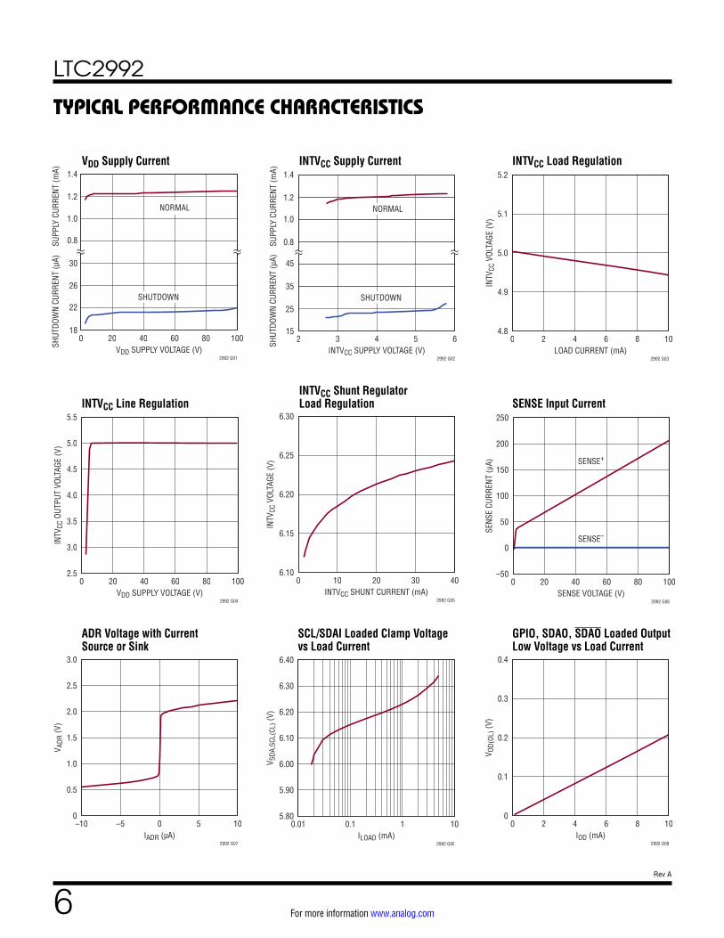
TYPICAL PERFORMANCE CHARACTERISTICS
VDD Supply Current INTVCC Supply Current INTVCC Load Regulation
INTVCC Line RegulationINTVCC Shunt Regulator Load Regulation SENSE Input Current
ADR Voltage with Current Source or Sink
SCL/SDAI Loaded Clamp Voltage vs Load Current
GPIO, SDAO, SDAO Loaded Output Low Voltage vs Load Current
VDD SUPPLY VOLTAGE (V)0 20 40 60 80 100
2.5
3.0
3.5
4.0
4.5
5.0
5.5
INTV
CC O
UTPU
T VO
LTAG
E (V
)
2992 G04
IADR (µA)–10 –5 0 5 10
0
0.5
1.0
1.5
2.0
2.5
3.0
V ADR
(V)
2992 G07ILOAD (mA)
0.01 0.1 1 105.80
5.90
6.00
6.10
6.20
6.30
6.40
V SDA
,SCL
(CL)
(V)
2992 G08IOD (mA)
0 2 4 6 8 100
0.1
0.2
0.3
0.4
V OD(
OL) (
V)
2992 G09
LOAD CURRENT (mA)0 2 4 6 8 10
4.8
4.9
5.0
5.1
5.2
INTV
CC V
OLTA
GE (V
)
2992 G03
NORMAL
SHUTDOWN
VDD SUPPLY VOLTAGE (V)0 20 40 60 80 100
0.8
1.0
1.2
1.4
18
22
26
30
SUPP
LY C
URRE
NT (m
A)SH
UTDO
WN
CURR
ENT
(µA)
2992 G01
NORMAL
SHUTDOWN
INTVCC SUPPLY VOLTAGE (V)2 3 4 5 6
0.8
1.0
1.2
1.4
15
25
35
45SU
PPLY
CUR
RENT
(mA)
SHUT
DOW
N CU
RREN
T (µ
A)
2992 G02
INTVCC SHUNT CURRENT (mA)0 10 20 30 40
6.10
6.15
6.20
6.25
6.30
INTV
CC V
OLTA
GE (V
)
2992 G05
SENSE+
SENSE–
SENSE VOLTAGE (V)0 20 40 60 80 100
–50
0
50
100
150
200
250
SENS
E CU
RREN
T (µ
A)
2992 G06

LTC2992
7Rev A
For more information www.analog.com
TYPICAL PERFORMANCE CHARACTERISTICS
ADC Error (GPIO) ADC Integral Nonlinearity (GPIO)ADC Differential Nonlinearity (GPIO)
ADC Error (∆SENSE)ADC Integral Nonlinearity (∆SENSE)
ADC Differential Nonlinearity (∆SENSE)
ADC Input Signal Attenuation (GPIO)
ADC Input Signal Attenuation(GPIO, Low Frequencies)
ADC Input Signal Attenuation(∆SENSE)
FREQUENCY (Hz)0 60 120 180 240
–80
–60
–40
–20
0
REJE
CTIO
N (d
B)
2992 G17
MAX ERROR
TYPICAL
12–BIT MODE
CODE0 1024 2048 3072 4096
–0.50
–0.25
0
0.25
0.50
ADC
ERRO
R (%
)
2992 G10CODE
0 1024 2048 3072 4096–0.3
–0.2
–0.1
0.0
0.1
0.2
0.3
ADC
INL
(LSB
)
2992 G11
12–BIT MODE
CODE0 1024 2048 3072 4096
–0.3
–0.2
–0.1
0.0
0.1
0.2
0.3
ADC
DNL
(LSB
)
2992 G12
12–BIT MODE
MAX ERROR
12–BIT MODE
TYPICAL
CODE0 1024 2048 3072 4096
–0.75
–0.50
–0.25
0
0.25
0.50
0.75
ADC
ERRO
R (%
)
2992 G13CODE
0 1024 2048 3072 4096–2.0
–1.0
0
1.0
2.0
ADC
INL
(LSB
)
2992 G14
12–BIT MODE
CODE0 1024 2048 3072 4096
–1.0
–0.5
0
0.5
1.0
ADC
DNL
(LSB
)
2992 G15
12–BIT MODE
FREQUENCY (kHz)
–100
–80
–60
–40
–20
0
REJE
CTIO
N (d
B)
2992 G16
0 62.5 125 187.5 250FREQUENCY (kHz)
–100
–80
–60
–40
–20
0
REJE
CTIO
N (d
B)
2992 G18
0 62.5 125 187.5 250

LTC2992
8Rev A
For more information www.analog.com
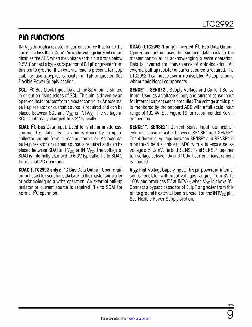
PIN FUNCTIONSADR1, ADR0: I2C Device Address Inputs. Connecting these pins to INTVCC, GND or leaving the pins open configures one of nine possible addresses. See Table 3 in Applications Information section for details.
EXPOSED PAD: Exposed Pad may be left open or connected to device ground. For best thermal performance, connect to a copper plane with an array of vias.
GND: Device Ground.
GPIO1, GPIO2: General Purpose Input/Output (Open Drain). Configurable to general purpose output, logic in-put, or data converter input. Tie to ground if unused. See Table 18 in Applications Information section for details.
GPIO3: General Purpose Input/Output (Open Drain). Configurable to general purpose output, logic input, data converter input or data ready signal (DATAREADY). As DATAREADY, it is latched low or pulses low for 16µs or 128µs when any of the ADC’s data becomes available. Tie to ground if unused. See Table 18 in Applications Informa-tion section for details.
GPIO4: General Purpose Input/Output (Open Drain). Configurable to general purpose output, logic input, data converter input or SMBus alert (ALERT). As ALERT, it is pulled to ground when a fault occurs to alert the host con-troller. A fault alert is enabled by setting the corresponding bit in the ALERT registers as shown in Tables 7, 11, 13 and 15. Tie to ground if unused. See Tables 18 and 19 in Applications Information section for details.
INTVCC: Internal Low Voltage Supply Input/Output. This pin is used to power internal circuitry. It can be configured as a direct input for a low voltage supply, as linear regula-tor from a higher voltage supply connected to VDD, or as a shunt regulator. Connect this pin directly to a 2.7V to 5.8V supply if available. When INTVCC is powered from an external supply, connect the VDD pin to INTVCC. If VDD is connected to a 8V to 100V supply, INTVCC becomes the 5V output of an internal series regulator that can supply up to 10mA to external circuitry. For even higher supply voltages or if a floating topology is desired, INTVCC can be used as a 6.2V shunt regulator. Connect the supply to
TYPICAL PERFORMANCE CHARACTERISTICS
ADC Input Signal Attenuation(∆SENSE, Low Frequencies)
Current Sense Amplifier Offset Drift Over Temperature
Current Sense Amplifier Offset Drift Over Input Common Mode
FREQUENCY (Hz)0 60 120 180 240
–80
–60
–40
–20
0
REJE
CTIO
N (d
B)
2992 G19
CALIBRATIONON
CALIBRATIONOFF
INITIAL CALIBRATION DONE AT VCM = 48V NO CALIBRATION THEREAFTER 12–BIT MODE
COMMON MODE VOLTAGE (V)0 25 50 75 100
–2
0
2
4
6
8
10
OFFS
ET D
RIFT
(LSB
)
2992 G21
CALIBRATIONON
CALIBRATIONOFF
INITIAL CALIBRATION DONE AT 25°CNO CALIBRATION THEREAFTER12–BIT MODE
TEMPERATURE (°C)–50 –25 0 25 50 75 100 125
–25
–15
–5
5
15
25
OFFS
ET D
RIFT
(LSB
)
2992 G20
LTC2992
9Rev A
For more information www.analog.com
PIN FUNCTIONSINTVCC through a resistor or current source that limits the current to less than 35mA. An undervoltage lockout circuit disables the ADC when the voltage at this pin drops below 2.5V. Connect a bypass capacitor of 0.1µF or greater from this pin to ground. If an external load is present, for loop stability, use a bypass capacitor of 1µF or greater. See Flexible Power Supply section.
SCL: I2C Bus Clock Input. Data at the SDAI pin is shifted in or out on rising edges of SCL. This pin is driven by an open-collector output from a master controller. An external pull-up resistor or current source is required and can be placed between SCL and VDD or INTVCC. The voltage at SCL is internally clamped to 6.3V typically.
SDAI: I2C Bus Data Input. Used for shifting in address, command or data bits. This pin is driven by an open-collector output from a master controller. An external pull-up resistor or current source is required and can be placed between SDAI and VDD or INTVCC. The voltage at SDAI is internally clamped to 6.3V typically. Tie to SDAO for normal I2C operation.
SDAO (LTC2992 only): I2C Bus Data Output. Open-drain output used for sending data back to the master controller or acknowledging a write operation. An external pull-up resistor or current source is required. Tie to SDAI for normal I2C operation.
SDAO (LTC2992-1 only): Inverted I2C Bus Data Output. Open-drain output used for sending data back to the master controller or acknowledging a write operation. Data is inverted for convenience of opto-isolation. An external pull-up resistor or current source is required. The LTC2992-1 cannot be used in nonisolated I2C applications without additional components.
SENSE1+, SENSE2+: Supply Voltage and Current Sense Input. Used as a voltage supply and current sense input for internal current sense amplifier. The voltage at this pin is monitored by the onboard ADC with a full-scale input range of 102.4V. See Figure 19 for recommended Kelvin connection.
SENSE1–, SENSE2–: Current Sense Input. Connect an external sense resistor between SENSE+ and SENSE–. The differential voltage between SENSE+ and SENSE– is monitored by the onboard ADC with a full-scale sense voltage of 51.2mV. Tie both SENSE– and SENSE+ together to a voltage between 0V and 100V if current measurement is unused.
VDD: High Voltage Supply Input. This pin powers an internal series regulator with input voltages ranging from 3V to 100V and produces 5V at INTVCC when VDD is above 8V. Connect a bypass capacitor of 0.1µF or greater from this pin to ground if external load is present on the INTVCC pin. See Flexible Power Supply section.

LTC2992
10Rev A
For more information www.analog.com
FUNCTIONAL DIAGRAM
TIMING DIAGRAM
tSU, DATtSU, STO
tSU, STA tBUFtHD, STA
tSP
tSPtHD, DATO,tHD, DATI
tHD, STA
STARTCONDITION
STOPCONDITION
REPEATED STARTCONDITION
REPEATED STARTCONDITION
2992 TD
SDA
SCL
SENSE1+
SENSE1–
VREF2.048V
6.3V
SENSE2–
SENSE2+
735kVDD
GND
IADC1
IADC2
2992 FD
VADCINTVCC
6.2V
5VLDO
–
+40X
–
+40X
1
2
16
15
8
7
12
3
14
4
13
735k
15k 15k
DECODER
ADR1 SDAO (LTC2992)SDAO (LTC2992-1)
ADR0SCLSDAI
S1
S2
G1
G2
G3
G4
I1 + I2
P1 + P2
I2
P2
I1
P1
12
12
12
I2C
1.23V
GPIO1
GPIO2
GPIO3
GPIO4
6.3V
–
+
10 9 6 5 11
4

LTC2992
11Rev A
For more information www.analog.com
OPERATIONThe LTC2992 accurately monitors current, voltage and power of two 0V to 100V supplies. An internal linear regulator allows the LTC2992 to operate directly from a 3V to 100V rail, or from an external supply voltage between 2.7V and 5.8V. Quiescent current is less than 1.6mA in normal operation. Enabling shutdown mode via the I2C interface reduces the quiescent current to below 50µA.
There are three onboard 8-/12-bit ADCs as shown in the Functional Diagram. Each supply’s load current is mea-sured with an external current sense resistor connected between SENSE+ and SENSE–. Internal amplifiers gain up the voltage drop across the sense resistor for monitoring by the IADCs (full-scale 51.2mV). VADC is used for voltage measurements and its input is selectively connected to SENSE1+, SENSE2+ (full-scale 102.4V) or any of the four GPIO pins (full-scale 2.048V). Each conversion takes 33ms for the IADCs and 16ms for the VADC in 12-bit mode. The conversion time can be shortened by a factor of 16 when 8-bit mode is selected.
The ADCs can be configured to run continuously (continu-ous scan) or on demand (snapshot mode). In continuous scan mode, the VADC measures selected voltages of the six inputs in round robin fashion. See the Applications Information section for more details. Status bits in the ADC STATUS register signal new conversion results from the ADCs have been written into onboard registers.
The GPIO1 to GPIO4 pins are also general purpose inputs or general purpose open-drain outputs. In addition, GPIO3 may be configured as DATAREADY output while GPIO4 is also an SMBus alert (ALERT) output. DATAREADY in-dicates availability of the most recent conversion results from any of the ADCs while ALERT indicates one or more faults have occurred.
Onboard memory stores the minimum and maximum values for each ADC measurement and calculates power data by digitally multiplying the stored current and voltage data. When the ADC measured value falls outside its pro-grammed window thresholds, a fault event is logged and the ALERT (GPIO4) may optionally pull low. The LTC2992 also calculates the total current and power consumption of the two monitored supplies.
The LTC2992 includes an I2C interface to access the onboard data registers and to program the alert thresh-old, configuration and control registers. Two three-state pins, ADR1 and ADR0, are decoded to allow nine device addresses (see Table 3). The SDA pin is split into SDAI (input) and SDAO (output, LTC2992) or SDAO (output, LTC2992-1) to facilitate opto-isolation. Tie SDAI and SDAO together for normal, nonisolated I2C operation.
LTC2992
12Rev A
For more information www.analog.com
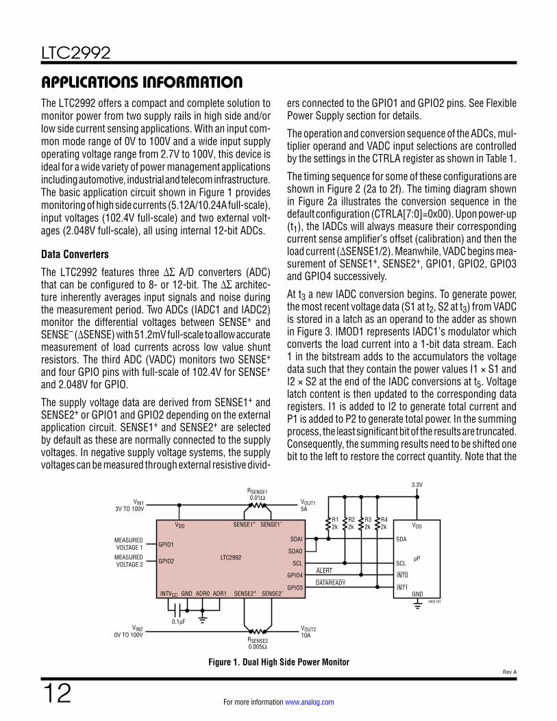
The LTC2992 offers a compact and complete solution to monitor power from two supply rails in high side and/or low side current sensing applications. With an input com-mon mode range of 0V to 100V and a wide input supply operating voltage range from 2.7V to 100V, this device is ideal for a wide variety of power management applications including automotive, industrial and telecom infrastructure. The basic application circuit shown in Figure 1 provides monitoring of high side currents (5.12A/10.24A full-scale), input voltages (102.4V full-scale) and two external volt-ages (2.048V full-scale), all using internal 12-bit ADCs.
Data Converters
The LTC2992 features three ∆∑ A/D converters (ADC) that can be configured to 8- or 12-bit. The ∆∑ architec-ture inherently averages input signals and noise during the measurement period. Two ADCs (IADC1 and IADC2) monitor the differential voltages between SENSE+ and SENSE– (∆SENSE) with 51.2mV full-scale to allow accurate measurement of load currents across low value shunt resistors. The third ADC (VADC) monitors two SENSE+
and four GPIO pins with full-scale of 102.4V for SENSE+ and 2.048V for GPIO.
The supply voltage data are derived from SENSE1+ and SENSE2+ or GPIO1 and GPIO2 depending on the external application circuit. SENSE1+ and SENSE2+ are selected by default as these are normally connected to the supply voltages. In negative supply voltage systems, the supply voltages can be measured through external resistive divid-
APPLICATIONS INFORMATIONers connected to the GPIO1 and GPIO2 pins. See Flexible Power Supply section for details.
The operation and conversion sequence of the ADCs, mul-tiplier operand and VADC input selections are controlled by the settings in the CTRLA register as shown in Table 1.
The timing sequence for some of these configurations are shown in Figure 2 (2a to 2f). The timing diagram shown in Figure 2a illustrates the conversion sequence in the default configuration (CTRLA[7:0]=0x00). Upon power-up (t1), the IADCs will always measure their corresponding current sense amplifier’s offset (calibration) and then the load current (∆SENSE1/2). Meanwhile, VADC begins mea-surement of SENSE1+, SENSE2+, GPIO1, GPIO2, GPIO3 and GPIO4 successively.
At t3 a new IADC conversion begins. To generate power, the most recent voltage data (S1 at t2, S2 at t3) from VADC is stored in a latch as an operand to the adder as shown in Figure 3. IMOD1 represents IADC1’s modulator which converts the load current into a 1-bit data stream. Each 1 in the bitstream adds to the accumulators the voltage data such that they contain the power values I1 × S1 and I2 × S2 at the end of the IADC conversions at t5. Voltage latch content is then updated to the corresponding data registers. I1 is added to I2 to generate total current and P1 is added to P2 to generate total power. In the summing process, the least significant bit of the results are truncated. Consequently, the summing results need to be shifted one bit to the left to restore the correct quantity. Note that the
Figure 1. Dual High Side Power Monitor
VDD
LTC2992
SDAI
SDAO
SCL
SDA
SCL
GPIO3
GPIO1
GPIO2
VIN13V TO 100V
VIN20V TO 100V
ALERT
VOUT15A
3.3V
VDD
µP
GND
R12k
R22k
R32k
R42k
VOUT210A
2992 F01
SENSE2+ SENSE2–
SENSE1+ SENSE1–
RSENSE10.01Ω
RSENSE20.005Ω
0.1μF
ADR0 ADR1GNDINTVCC
GPIO4
INT1
INT0DATAREADY
MEASUREDVOLTAGE 2
MEASUREDVOLTAGE 1

LTC2992
13Rev A
For more information www.analog.com
calculated LSB (see Design Example section) for current and power of both supplies have to match. Otherwise, external µP can be used to first compute physical amount of current and power for each supply and then perform the summing.
The LTC2992 measures the current sense amplifier’s input offset to calibrate subsequent IADC measurements. During offset measurement, IADC cannot capture load current information. By default, such calibration is done for every IADC conversion as shown in Figure 2a. In most applications, the calibration frequency can be reduced by writing to CTRLA register with its CTRLA[7] bit set to 1. A one-off calibration is then performed immediately after the I2C write operation as shown in Figure 2b.
VADC by default monitors six input voltages sequentially as shown in Figure 2a with an update rate of 10Hz for each
APPLICATIONS INFORMATIONinput. Therefore, input signals such as supply rail voltages with average value that varies at less than 5Hz can be ac-curately monitored. Otherwise, the input update rate can be increased by reducing the number of inputs monitored via CTRLA[4:3]. Figure 2c shows only the SENSE+ pins being monitored in continuous scan mode with an effec-tive update rate of 30Hz. The remaining inputs may be monitored by switching to snapshot mode when needed.
A snapshot mode is available to make on-demand mea-surement of a single selected voltage without power data update (SENSE1+, SENSE2+, GPIO1, GPIO2, GPIO3 or GPIO4) or two selected voltages (either SENSE1+ and SENSE2+, or GPIO1 and GPIO2). To make a snapshot mea-surement, write the 3-bit code of the desired voltage input to CTRLA[2:0] and 01 to CTRLA[6:5]. After completion of the conversion, the ADCs will halt and the corresponding
Table 1. ADC Configuration Via CTRLA RegisterBIT NAME OPERATION
CTRLA[7] Offset Calibration Offset Calibration for Current Measurements [1] = Calibrate on Demand [0] = Every Conversion (Default)
CTRLA[6:5] Measurement Mode
[11] = Shutdown [10] = Single Cycle mode The VADC converts SENSE1+, SENSE2+, GPIO1, GPIO2, GPIO3, GPIO4 once and stops. The IADCs stop after one conversion. P1 = SENSE1+ × ∆SENSE1; P2 = SENSE2+ × ∆SENSE2 [01] = Snapshot Mode Snapshot Initializes Conversion on All 3 ADCs Simultaneously. VADC Converts the Channel(s) per CTRLA[2:0] [00] = Continuous Scan Mode (Default) The Selected Channels for VADC are Defined by CTRLA[4:3]
CTRLA[4:3] Voltage Selection for Continuous Scan Mode
CTRLA[4:3] VADC P1 P211 GPIO1, GPIO2,
GPIO3, GPIO4GPIO1 × ∆SENSE1 GPIO2 × ∆SENSE2
10 GPIO1, GPIO2 GPIO1 × ∆SENSE1 GPIO2 × ∆SENSE201 SENSE1+, SENSE2+ SENSE1+ × ∆SENSE1 SENSE2+ × ∆SENSE200 (Default) SENSE1+, SENSE2+,
GPIO1, GPIO2, GPIO3, GPIO4
SENSE1+ × ∆SENSE1 SENSE2+ × ∆SENSE2
CTRLA[2:0] Voltage Selection for Snapshot Mode
CTRLA[2:0] VADC P1 P2111 GPIO1, GPIO2 GPIO1 × ∆SENSE1 GPIO2 × ∆SENSE2110 SENSE1+, SENSE2+ SENSE1+ × ∆SENSE1 SENSE2+ × ∆SENSE2101 GPIO4 ∆SENSE1/2 without P1/P2 updates100 GPIO3011 GPIO2010 GPIO1001 SENSE2+
000 (Default) SENSE1+

LTC2992
14Rev A
For more information www.analog.com
APPLICATIONS INFORMATION
Figure 2
2992 F02
POWER UP
S1 S2 G1 G2 G3 G4 S1 S2 G1 G2VADC
t1 t2 t3 t4 t5 t6 t7 t8 t9 t1016.4ms 16.4ms 16.4ms 16.4ms 16.4ms 16.4ms 16.4ms 16.4ms 16.4ms
CAL I1 AND P1 CAL I1 AND P1 CALIADC1
CAL
(2a) Continuous Scan Mode with Calibration Every Cycle (Default) S1, S2, G1, G2, G3, G4: SENSE1+, SENSE2+, GPIO1, GPIO2, GPIO3, and GPIO4 CAL: Calibration of Current Sense Amplifier I1, I2: ∆SENSE1, ∆SENSE2 P1, P2: POWER1, POWER2
I2 AND P2 CAL I2 AND P2 CALIADC2
S1 S2 G1 G2 G3 G4 S1 S2 S2 G1 G2S1VADC
CAL I1 AND P1 I1 AND P1 I1 AND P1 CALIADC1
CAL
(2b) Continuous Scan Mode with On-Demand Calibration. CTRLA[7:0] = 0x80
I2 AND P2 I2 AND P2 I2 AND P2 CAL
WRITE 0x80 TOCTRLA REGISTER
WRITE 0x80 TOCTRLA REGISTER
IADC2
I1 AND P1
I2 AND P2
S1 S2 S1 S2 S1 S2VADC
CAL I1 AND P1 I1 AND P1IADC1
CAL
(2c) Continuous Scan Mode with On-Demand Calibration. CTRLA[7:0] = 0x88
I2 AND P2 I2 AND P2
WRITE 0x88 TOCTRLA REGISTER
IADC2
S1 S2 G1 G2 G3 G4VADC
CAL I1 AND P1 IDLEIADC1
CAL I2 AND P2 IDLE
WRITE 0x40 TOCTRLA REGISTER
IADC2
S1 IDLEVADC
CAL I1 IDLEIADC1
CAL
(2d) Snapshot Mode for Single Voltage. CTRLA[7:0] = 0x20
I2 IDLE
WRITE 0x20 TOCTRLA REGISTER
IADC2
G1 G2VADC
CAL I1 AND P1 IDLE
IDLE
IADC1
CAL
(2e) Snapshot Mode for Two Voltages. CTRLA[7:0] = 0x27
I2 AND P2 IDLE
WRITE 0x27 TOCTRLA REGISTER
IADC2
(2f) Single Cycle Mode. CTRLA[7:0] = 0x40
IDLE
t1 t2 t3 t4 t5 t6 t7

LTC2992
15Rev A
For more information www.analog.com
bits in ADC STATUS register (Table 10) are set to indicate the availability of new data. An alert may be generated at the end of a snapshot conversion by setting bit AL4[7:6] in the ALERT4 register (Table 15). To make another snap-shot measurement, rewrite the CTRLA register. Figure 2d shows a snapshot operation of SENSE1+ with no updates to power data since only single voltage is selected while Figure 2e shows combo snapshot operation of GPIO1 and GPIO2 with new power data.
A single cycle mode allows all six voltages to be measured once with a single I2C command. To initiate such mode, write 10 to CTRLA[6:5] as shown in Figure 2f. SENSE1+, SENSE2+ are updated together with current and power values at t5. At t7 the conversions are done and the ADCs are halted.
If there is an extended period of I2C communication between the LTC2992 and the controller, some of the ADC result may be lost. This is because during the I2C communica-tion, the ADCs are prevented from updating the internal registers to avoid corrupting the data. This problem can be overcome by breaking the I2C communication into blocks of less than one conversion period (16.4ms for 12-bit mode and 1ms for 8-bit mode).
Flexible Power Supply
The LTC2992 can be externally configured to derive power from a wide range of supplies. The LTC2992 includes an onboard linear regulator to power the low voltage inter-nal circuitry connected to the INTVCC pin from high VDD voltages. The linear regulator operates with VDD voltages from 3V to 100V, and a shunt regulator is available for voltages above 100V. The linear regulator produces a 5V output capable of supplying 10mA at the INTVCC pin when VDD is greater than 8V. The regulator is disabled when the
APPLICATIONS INFORMATIONjunction temperature rises above 150°C, and the output is protected against accidental shorts. Bypass capacitors of 0.1μF, or greater, at both the VDD and INTVCC pins are recommended for optimal transient performance. Note that operation with high VDD voltages can result in significant power dissipation, and care is required to ensure that the maximum operating junction temperature stays below 125°C. For improved thermal resistance, use the DFN package and solder the exposed pad to a large copper region on the PCB.
Figure 4a shows the LTC2992 being used to monitor input supplies that range from 4V to 100V. No separate supply is needed since VDD can be connected to either of the input supplies. To prevent loss of operation from either supply’s failure, VDD is connected to VIN1 and VIN2 via diodes. If the LTC2992 is used to monitor input supplies of 0V to 100V, it can derive power from a wide range separate sup-ply connected to the VDD pin as shown in Figure 4b. The
(4b) Derives Power from a Separate Wide Range Supply
(4a) Derives Power from the Supplies Being Monitored
Figure 3. POWER1 Generator Blocks
VDD
GND
LTC2992
VIN10V TO 100V
3V TO 100V
VIN20V TO 100V
VOUT1
VOUT2
INTVCC
2992 F04b
SENSE2+ SENSE2–
SENSE1+ SENSE1–
RSENSE10.01Ω
RSENSE20.005Ω
C2
VDD
GND
BAV23CLT1G
LTC2992
VIN14V TO 100V
VIN24V TO 100V
VOUT1
VOUT2
INTVCC
2992 F04a
SENSE2+ SENSE2–
SENSE1+ SENSE1–
RSENSE10.01Ω
RSENSE20.005Ω
C2
VOLTAGELATCH
ACCUMULATORLATCH
POWER1
IMOD1
VADCDATA
2992 F03
+
LTC2992
16Rev A
For more information www.analog.com
APPLICATIONS INFORMATION
(5a) Derives Power Through a Low Side Shunt Regulator in a High Side Current Sense Topology
(5c) Recommended Layout for Figure 5b’s SENSE Pins Connection
(5b) Derives Power from the Supply Monitored in a Low Side Current Sense Topology
(4c) Derives Power from a Separate Low Voltage Supply
SENSE+/– pins can be biased independently of the part’s supply voltage. Alternatively, if a low voltage supply is present it can be connected to the INTVCC pin, as shown in Figure 4c, to minimize on-chip power dissipation. When INTVCC is powered from a separate supply, connect VDD to INTVCC.
VDD
GND
LTC2992
VIN10V TO 100V
2.7V TO 5.8V
VIN20V TO 100V
VOUT1
VOUT2
INTVCC
2992 F04c
SENSE2+ SENSE2–
SENSE1+ SENSE1–
RSENSE10.01Ω
RSENSE20.005Ω
VDD
GND
LTC2992
VIN10V TO 100V
> 100V
VIN20V TO 100V
VOUT1
VOUT2
INTVCC
RSHUNT
2992 F05a
SENSE2+ SENSE2–
SENSE1+ SENSE1–
RSENSE10.01Ω
RSENSE20.005Ω
C2
(VOUT) close to the SENSE+ terminal of the sense resistors with a wide track to prevent excessive potential difference between the SENSE+ pins when load current is supplied entirely by VIN1 or VIN2.
Supply Undervoltage Lockout
During power-up, the internal I2C logic and the ADCs are enabled when either VDD or INTVCC rises above its under-voltage lockout threshold (2.7V for VDD and 2.5V for INTVCC typically). During power-down, the ADCs are disabled when VDD and INTVCC fall below their respective
RSENSE2
VOUT
VIN2
VIN1
RSENSE1MBR10100
MBR10100
2992 F05c
17
16 15 14 13 12 11 10 9
1 2 3 4 5 6 7 8
BOTTOM LAYER
TOP LAYER
GPIO2 GNDC2
INTVCC
LTC2992
VDD
VOUT5A
GPIO1
R1120k
2992 F05b
SENSE2– SENSE2+SENSE1– SENSE1+
RSENSE20.01Ω
RSENSE10.01Ω
VIN2–5V TO –100V
RTN1 RTN
RTN2
VIN1–5V TO –100V
MBR10100
MBR10100
R91M
R1020k
R81M
MBR10100
MBR10100
Figure 5a shows a high side rail-to-rail power monitor which derives power from a separate supply greater than 100V. The voltage at INTVCC is clamped at 6.3V above ground in a low side shunt regulator configuration to power the part.
In dual feed, low side power monitor applications, the device ground and the current sense inputs are connected to the diode-ORed output of the input supplies’ negative terminal as shown in Figure 5b. Note that the SENSE– pins operate at a voltage more negative than the device ground. It is highly recommended that the SENSE+ pins be operating at as close to device ground potential as possible so that at full-scale the SENSE– pins are limited to 80mV below device ground for accurate measurements. A recom-mended layout for Figure 5b’s SENSE pins connection is shown in Figure 5c. Layout the common connection

LTC2992
17Rev A
For more information www.analog.com
APPLICATIONS INFORMATIONundervoltage lockout thresholds. If VDD or INTVCC remains above their typical 2.1V I2C reset threshold, the internal I2C logic retains the state before power-down. If VDD or INTVCCis then increased as in a normal power-up, the ADCs will run according to CTRLA register’s setting at that point in time. The internal I2C logic is reset when VDD and INTVCC fall below their respective I2C reset thresholds.
Shutdown Mode
The LTC2992 includes a low quiescent current shutdown mode, controlled by bits CTRLA[6:5] in the CTRLA register (Table 1). Setting CTRLA[6:5]=11 puts the part in shutdown mode, powering down the ADC, internal reference and on-board linear regulator. The internal I2C bus remains active, and although the ADR1 and ADR0 pins are disabled, the device will retain the most recently programmed I2C bus address. All onboard registers retain their contents and can be accessed through the I2C interface. To re-enable ADC conversions, reset bit CTRLA[6:5] in the CTRLA register. The analog circuitry will power up and all registers will retain their contents.
The onboard linear regulator is disabled in shutdown mode to conserve power. If the onboard linear regulator is used to power external I2C bus related circuitry such as opto-couplers or pull-ups, I2C communication will be lost when the part is shut down. The LTC2992 would then have to be reset by cycling its power to come out of shutdown. If low IQ mode is not required, ensure 11 cannot be written to CTRLA[6:5] in the CTRLA register during software de-velopment. It is recommended that external regulators be used in such applications if powering down the LTC2992 is desirable. As an added layer of protection against this scenario, bit CTRLB[4] in the CTRLB register can be set during system configuration to enable the LTC2992 to automatically exit shutdown mode when the I2C lines are low for more than 33ms (which can be a result of accidental shutdown of the LTC2992’s linear regulator powering the I2C). The user can elect to be alerted of this event by setting bit AL4[4] in the ALERT4 register (Table 15). Quiescent current drops below 50μA in shutdown mode with the internal regulator disabled.
Configuring the GPIO Pins
The LTC2992 has four GPIO pins configurable through the GPIO IO CONTROL register (Table 18) to be used as general purpose input/output pins. By configuring the CTRLA register, the voltage at the four GPIO pins can be measured by the VADC. GPIO1 through GPIO4 have comparators monitoring the voltage on these pins with a threshold of 1.23V typically, the results of which may be read from bits GS[3:0] in the GPIO STATUS register, as shown in Table 17. An alert may be generated, when GPIO1, GPIO2 or GPIO3 cross the comparator threshold voltage (1.23V typical), by setting bits AL4[3:1], respectively, in the ALERT4 register.
GPIO1, GPIO2, GPIO3 and GPIO4 can be pulled low as general purpose outputs, which are otherwise high im-pedance. GPIO3 can also be used as a data ready output (DATAREADY) to indicate new data from any of the three ADCs by configuring GIO[5:4] in the GPIO IO CONTROL register. The output can be in the form of a low pulse with duration of 16µs or 128µs or a latched low state. The ADC STATUS register (Table 10) indicates which of the moni-tored voltages has been recently updated. This register is cleared-on-read, which will also release the GPIO3 from its latched low state.
GPIO4 is by default an SMBus alert (ALERT) output that pulls low when an alert event is present. To pull GPIO4 (ALERT) low in the absence of an alert event, set GC[7] of the GPIO4 CONTROL register (Table 19). Clearing this bit will release the GPIO4 (ALERT). GC[7] is set whenever an alert event occurs. Setting GC[6] will similarly pull GPIO4 low.
I2C Reset
To avoid the need of power-cycling the part for a reset, LTC2992 features a software reset which is enabled by setting CTRLB[0] of CTRLB register (Table 6). This bit is self-cleared. All internal registers except the present value data registers are reset to their default states. The ADCs will sample continuously after reset without any reconfiguration since this is the default behavior.

LTC2992
18Rev A
For more information www.analog.com
APPLICATIONS INFORMATIONStoring Minimum and Maximum Values
The LTC2992 compares each measurement including the calculated power with the stored values in the respective MIN and MAX registers for each parameter (Table 4). If the new conversion is beyond the stored minimum or maximum values, the MIN or MAX registers are updated with the new values. The MIN and MAX registers are refreshed only when ADCs update the internal registers. Writing via I2C to the ADC registers does not affect the MIN and MAX registers. To initiate a new peak hold cycle for all measurements, set CTRLB[3] of CTRLB register (Table 6). This bit is self-cleared. For new peak hold cycle of selective measurement, write all 1’s to its MIN regis-ter and all 0’s to its MAX register via the I2C bus. These registers will be updated when the next respective ADC conversion is done.
The LTC2992 also includes MIN and MAX threshold reg-isters (Table 4) for the measured parameters including the calculated power. At power-up or reset by I2C command, the MAX threshold registers are set to all 1’s, and MIN threshold registers are set to all 0’s, effectively disabling them. The MIN and MAX threshold registers can be repro-grammed to any desired value via the I2C bus.
Fault Alert and Resetting Faults
As soon as a measured quantity falls below the minimum threshold or exceeds the maximum threshold, the LTC2992 sets the corresponding flag in the FAULT1 (Table 8), FAULT2 (Table 12) and FAULT3 registers (Table 14). Other events such as GPIO state change have their present status in the GPIO STATUS (Table 17) register and any fault is latched in the FAULT4 (Table 16) register. The GPIO4 pin is pulled low if the appropriate bit in the ALERT1 (Table 7), ALERT2 (Table 11), ALERT3 (Table 13) and ALERT4 (Table 15) registers is set when the fault occurs. More details on the alert behavior can be found in the Alert Response Protocol section.
An active fault indication can be reset by writing zeros to the corresponding FAULT register bits or setting bit CTRLB[5] in the CTRLB register. If bit CTRLB[5] is set, reading the fault register will cause the corresponding register to reset. All FAULT register bits are also cleared
if the VDD and INTVCC fall below their respective I2C logic reset threshold.
ADC Resolution and Conversion Rate
The resolution of the ADCs can be configured to 8-bit by setting bit NADC[7] of NADC register (Table 9) through an I2C write command to speed up ADC conversions.
Table 2. ADC Resolution and Conversion RateRESOLUTION 12-BIT 8-BITNADC[7] 0 1Conversion Time SENSE+, GPIO 16.4ms 1.02ms
∆SENSE* 65.6ms 4.1msLSB Step Size SENSE+ 25mV 400mV
GPIO 0.5mV 8mV∆SENSE 12.5μV 200μV
*Snapshot mode
If the resolution is changed while an ADC conversion is in progress, that conversion will be aborted. In continu-ous scan mode, a new conversion of the same quantity will be started with the new resolution and continues in the original sequence. Otherwise, a new snapshot of one, two or multiple quantities (single cycle) will take place. Resetting the peak hold registers by setting CTRLB[3] in the CTRLB register via I2C bus prior to changing the ADC resolution is recommended to ensure integrity of the peak hold values.
The data format in 8-bit mode for voltage/current is left justified by four bits and power is left justified by eight bits with respect to the 12-bit’s format as shown in Figure 6.
POWER REGISTER VALUE
MODE BIT
23:20 19:16 15:12 11:8 7:4 3:0
12-bit Data Data Data Data Data Data
8-bit Data Data Data Data 0x0 0x0
VOLTAGE/CURRENT REGISTER VALUE
MODE BIT
15:12 11:8 7:4 3:0
12-bit Data Data Data 0x0
8-bit Data Data 0x0 0x0
Figure 6. Data Format in 12-Bit and 8-Bit Mode

LTC2992
19Rev A
For more information www.analog.com
Figure 7. Configuring GPIO3 as DATAREADY
ADC Status and Data Ready Signal
ADC STATUS register (Table 10) indicates availability of new measurement results in the internal registers and is reset after it is read via I2C bus. Details on configuring GPIO3 as DATAREADY can be found in Configuring the GPIO Pins section. To illustrate the behavior of DATAREADY as new data becomes available, an example in which the ADCs are continuously converting is shown in Figure 7. GPIO3 is initially configured to output a 16µs low pulse with new data as is seen at t4 and t5. As S1 and S2 data are updated together with I1 and I2 at t5, no GPIO3 pulse is seen at t2 and t3. GPIO3 is then reconfigured to latch low with new data—this happens at t6. GPIO3 is released from its latched state when an I2C read command to ADC STATUS register is done.
Crosstalk Mitigation
The GPIO pins are general purpose pins that can be used to monitor digital or analog signals. Even with an averaging architecture of the ∆∑ ADCs, crosstalk may still be prob-lematic if an application requires monitoring of precision analog signals and noisy digital signals with the GPIO pins.
To preserve measurement accuracy of the analog signals, a few measures can be taken:
1. Physically separate the clean and noisy signals. For ex-ample, the clean signal may be monitored with GPIO1/3 while the noisy signal is monitored with GPIO2/4 on the other side of the part.
2. If adjacent GPIO pins have to be used, then decouple the analog signal to device ground near the GPIO pin with an external capacitor. Typically, a capacitance of 0.1µF should suffice.
3. Shield the sensitive signal with ground.
4. In a multi-layer PCB, the sensitive signal should be routed mostly sandwiched between two ground layers and exit next to the part for connection to the pin.
A layout example is given in Layout Considerations section for two-layered board design.
I2C Interface
The LTC2992 includes an I2C/SMBus-compatible interface to provide access to the onboard registers. Figure 8 shows a general data transfer format using the I2C bus.
The LTC2992 is a read/write slave device and supports the SMBus read byte, write byte, read word and write word protocols. The LTC2992 also supports extended read and write commands that allow reading or writing more than two bytes of data. When using the read/write word or extended read and write commands, the bus master issues an initial register address and the internal register address pointer automatically increments by 1 after each byte of data is read or written. After the register address reaches 0x97, it will roll over to 0x00 and continue incre-menting. A STOP condition resets the register address pointer to 0x00. The data formats for the above commands are shown in Figure 8 through Figure 14. Note that only
APPLICATIONS INFORMATION
2992 F07
POWER UPt1 t2 t3 t4 t5 t6 t7 t8
16µs PULSE
S2S1 G2G1 G4G3 S2S1VADC
CAL I1 AND P1 CAL I1 AND P1IADC1
CAL I2 AND P2 CAL I2 AND P2IADC2
GPIO3
I2C BUSESWRITEREG: 0x96DATA: 0x12
READREG: 0x32DATA: 0x00
READREG: 0x32DATA: 0x00
WRITEREG: 0x96DATA: 0x32
READREG: 0x32DATA: 0xFF
IDLE IDLE IDLE IDLE IDLE

LTC2992
20Rev A
For more information www.analog.com
APPLICATIONS INFORMATIONthe read byte command is available to the 0xE7 and 0xE8 (MFR_SPECIAL_ID) registers (Table 4).
I2C Device Addressing
Nine distinct I2C bus addresses are configurable using the three-state pins ADR0 and ADR1, as shown in Table 3. ADR0 and ADR1 should be tied to INTVCC, to GND, or left floating (NC) to configure the lower four address bits. During low power shutdown, the address select state is latched into memory powered from standby supply. Address bits a6, a5 and a4 are permanently set to 110 and the least significant bit is the R/W bit. In addition, all LTC2992 devices will respond to a common mass write address (1100110)b; this allows the bus master to write
to several LTC2992s simultaneously, regardless of their individual address settings. The LTC2992 will also respond to the standard SMBus ARA address (0001100)b if the GPIO4 (ALERT) pin is asserted. See the Alert Response Protocol section for more details. The LTC2992 will not respond to the ARA address if no alerts are pending.
Start and Stop Conditions
When the I2C bus is idle, both SCL and SDA are in the high state. A bus master signals the beginning of a transmis-sion with a START condition by transitioning SDA from high to low while SCL stays high. When the master has finished communicating with the slave, it issues a STOP
Figure 8. General Data Transfer Over I2C
Figure 9. Serial Bus SDA Write Byte Protocol
Figure 10. Serial Bus SDA Write Word Protocol
Figure 11. Serial Bus SDA Write Page Protocol Figure 12. Serial Bus SDA Read Byte Protocol
Figure 14. Serial Bus SDA Read Page Protocol
Figure 13. Serial Bus SDA Read Word Protocol
SDA
SCL
S P
a6 - a0 b7 - b0 b7 - b0
1 - 7 1 - 7 1 - 78 8 89 9 9
STARTCONDITION
STOPCONDITION
ADDRESS ACK DATA DATAACK ACKR/W
2992 F08
S ADDRESS
1 1 0 a3:a0
FROM MASTER TO SLAVE
FROM SLAVE TO MASTER
A: ACKNOWLEDGE (LOW)A: NOT ACKNOWLEDGE (HIGH)R: READ BIT (HIGH)
COMMAND DATA
b7:b00
W
0 0 0b7:b0
A A A P
2992 F09
W: WRITE BIT (LOW)S: START CONDITIONP: STOP CONDITION
S ADDRESS1 1 0 a3:a0
COMMAND DATA DATAb7:b00
W0 0 0 0
2992 F10
b7:b0b7:b0
A A A A P
S ADDRESS1 1 0 a3:a0
COMMAND0b7:b00
W0 0
2992 F11
A A A Pb7:b0DATA
0A
b7:b0DATA
0A
......
b7:b0DATA S ADDRESS
1 1 0 a3:a0 1 1 0 a3:a0 1 0COMMAND S ADDRESS R A
b7:b0 1DATA
b7:b00W
0 02992 F12
A A A P
S ADDRESS1 1 0 a3:a0 1 1 0 a3:a0 1 0
COMMAND S ADDRESS R Ab7:b0 1
DATAb7:b00
W0 0
2992 F13
A0
Ab7:b0
DATAA A P
S ADDRESS1 1 0 a3:a0 1 1 0 a3:a0 1 0
COMMAND S ADDRESS R Ab7:b0 1
DATAb7:b00
W0 0
2992 F14
A0
Ab7:b0
DATAA A P...
...b7:b0
DATA
LTC2992
21Rev A
For more information www.analog.com
APPLICATIONS INFORMATIONcondition by transitioning SDA from low to high while SCL stays high. The bus is then free for another transmission.
Stuck-Bus Reset
The LTC2992 I2C interface features a stuck-bus reset timer to prevent it from holding the bus lines low indefinitely if the SCL signal is interrupted during a transfer. The timer starts when either SCL or SDAI is low, and resets when both SCL and SDAI are pulled high. If either SCL or SDAI are low for over 33ms, the stuck-bus timer will expire, and the internal I2C interface and the SDAO pin pull-down logic will be reset to release the bus. Normal communication will resume at the next START command.
Acknowledge
The acknowledge signal is used for handshaking between the master and the slave to indicate that the last byte of data was received. The master always releases the SDA line during the acknowledge clock pulse. The LTC2992 will pull the SDA line low on the 9th clock cycle to acknowledge receipt of the data. If the slave fails to acknowledge by leaving SDA high, then the master can abort the transmis-sion by generating a STOP condition. When the master is receiving data from the slave, the master must acknowledge the slave by pulling down the SDA line during the 9th clock pulse to indicate receipt of a data byte. After the last byte has been received by the master, it will leave the SDA line high (not acknowledge) and issue a STOP condition to terminate the transmission.
Write Protocol
The master begins a write operation with a START condi-tion followed by the 7-bit slave address and the R/W bit set to zero. After the addressed LTC2992 acknowledges the address byte, the master then sends a command byte that indicates which internal register the master wishes to write. The LTC2992 acknowledges this and then latches the command byte into its internal register address pointer. The master then delivers the data byte and the LTC2992 acknowledges once more and writes the data into the in-ternal register pointed to by the register address pointer. If the master continues sending additional data bytes with a write word or extended write command, the additional data
bytes will be acknowledged by the LTC2992, the register address pointer will automatically increment by one, and data will be written as previously stated. The write opera-tion terminates and the register address pointer resets to 0x00 when the master sends a STOP condition.
Read Protocol
The master begins a read operation with a START condi-tion followed by the 7-bit slave address and the R/W bit set to zero. After the addressed LTC2992 acknowledges the address byte, the master then sends a command byte that indicates which internal register the master wishes to read. The LTC2992 acknowledges this and then latches the command byte into its internal register address pointer. The master then sends a repeated START condition fol-lowed by the same 7-bit address with the R/W bit now set to 1. The LTC2992 acknowledges and sends the contents of the requested register. The transmission terminates when the master sends a STOP condition. If the master acknowledges the transmitted data byte, as in a read word command, the LTC2992 will send the contents of the next register. If the master keeps acknowledging, the LTC2992 will keep incrementing the register address pointer and sending out data bytes. The read operation terminates and the register address pointer resets to 0x00 when the master sends a STOP condition.
Alert Response Protocol
When any of the fault bits in the fault registers (FAULT1, FAULT2, FAULT3 and FAULT4) are set, a bus alert is gener-ated if the appropriate bit in the ALERT1, ALERT2, ALERT3 or ALERT4 registers has been set. This allows the bus master to select which faults will generate alerts. At power-up, all ALERT registers are cleared (no alerts enabled) and the GPIO4 (ALERT) pin is high. If an alert is enabled, the corresponding fault causes the GPIO4 (ALERT) pin to pull low. The bus master responds to the alert in accordance with the SMBus alert response protocol by broadcasting the alert response address (0001100)b, and the LTC2992 replies with its own address and releases its GPIO4 (ALERT) pin, as shown in Figure 15. The GPIO4 (ALERT) line is also released if CTRLB[7] is set and the LTC2992 is addressed (see Table 6) by any message. The GPIO4 (ALERT) signal

LTC2992
22Rev A
For more information www.analog.com
is not pulled low again until the fault registers indicate a different fault has occurred or the original fault is cleared and it occurs again. Note that this means repeated or continuing faults will not generate additional alerts until the associated fault register bits have been cleared.
Figure 15. Serial Bus SDA Alert Response Protocol
open-drain opto-isolators can use the LTC2992 with the SDAI and SDAO pins separated, as shown in Figure 16. Connect SDAI to the output of the incoming opto-isolator with a pull-up resistor to INTVCC or a local 5V supply; con-nect SDAO to the cathode of the outgoing opto-isolator with a current-limiting resistor in series with the anode. The input and output must be connected together on the isolated side of the bus to allow the LTC2992 to participate in I2C arbitration. Note that maximum I2C bus speed will generally be limited by the speed of the opto-couplers used in this application.
Figure 17 shows an alternate connection for use with low speed opto-couplers and the LTC2992-1. This circuit uses a limited-current pull-up on the internally clamped SDAI pin and clamps the SDAO pin with the input diode of the outgoing opto-isolator, removing the need to use INTVCC for biasing in the absence of a separate low voltage sup-ply. For proper clamping:
VIN(MAX) – VSDA,SCL(MIN)
ISDA,SCL(MAX)≤R4≤
VIN(MIN) – VSDA,SCL(MAX)
ISDA,SCL(MIN)
VIN(MAX) – 5.9V
5mA≤R4≤
VIN(MIN) – 6.9V
0.5mA
(1)
As an example, a supply that operates from 36V to 72V would require the value of R4 to be between 13k and 58k. The LTC2992-1 must be used in this application to ensure that SDAO signal polarity is correct. R4 may
APPLICATIONS INFORMATION
SCL
5V
SDAI
SDAO
GND
LTC2992SCL
3.3V
VDD
SDAGND
µP
1/2 MOCD207M
MOCD207M
2992 F16
R44.7k
R54.7k
R70.47k
R80.47k
R102k
R60.82k
Figure 16. Opto-Isolation of a 10kHz I2C Interface Between LTC2992 and Microcontroller
Figure 17. Opto-Isolation of a 1.5kHz I2C Interface Between LTC2992-1 and Microcontroller (SCL Omitted for Clarity)
VIN48V
SDAI
SDAOGND
LTC2992-1
3.3V
VDD
SDAGND
µP
1/2 MOCD207M
1/2 MOCD207M
2992 F17
R420k R6
0.51kR72k
R55.1k
SALERT
RESPONSEADDRESS
R A
10 0 0 1 1 0 0 1 2992 F150
A P
a7:a0
DEVICEADDRESS
If two or more LTC2992s on the same bus are generat-ing alerts when the ARA is broadcast, the bus master will repeat the alert response protocol until the GPIO4 (ALERT) line is released. Standard I2C arbitration causes the device with the highest priority (lowest address) to reply first and the device with the lowest priority (highest address) to reply last.
Opto-Isolating the I2C Bus
Opto-isolating a standard I2C device is complicated by the bidirectional SDA pin. The LTC2992/LTC2992-1 minimize this problem by splitting the standard I2C SDA line into SDAI (input) and SDAO (output, LTC2992) or SDAO (inverted output, LTC2992-1). The SCL is an input-only pin and does not require special circuitry to isolate. For conventional nonisolated I2C applications, use the LTC2992 and tie the SDAI and SDAO pins together to form a standard I2C SDA pin. Low speed isolated interfaces that use standard

LTC2992
23Rev A
For more information www.analog.com
be split into two or more series connected units to meet thermal requirements.
The LTC2992 can also be used with high speed optocou-plers with push-pull outputs and inverted logic as shown in Figure 18. The incoming opto-isolator draws power from INTVCC, and the data output is connected directly to the SDAI pin with no pull-up required. Ensure current drawn does not exceed the 10mA maximum capability of the INTVCC pin. The SDAO pin is connected to the cathode of the outgoing opto-coupler with a current limiting resistor connected back to INTVCC. An additional discrete diode is required at the output of the outgoing opto-coupler to provide the open-drain pull-down that the I2C requires. Finally, the input of the incoming opto-isolator is connected back to the output as in the low speed case.
Layout Considerations
A Kelvin connection between the sense resistor RSNS and the LTC2992 is recommended to achieve accurate current sensing (Figure 19). The recommended minimum trace width for 1oz copper foil is 0.02˝ per amp to ensure the trace stays at a reasonable temperature. Using 0.03˝ per amp or wider is preferred. Note that 1oz copper exhibits a sheet resistance of about 530μΩ per square. In very high current applications where the sense resistor can dissipate significant power, the PCB layout should include good thermal management techniques such as extra vias and wide metal area. 2oz or thicker copper should be considered for such applications. The trace from sense resistors to SENSE+ pins should be as short as possible to minimize IR drop due to pin current.
APPLICATIONS INFORMATION
Figure 19. Recommended PCB Layout
Figure 18. Opto-Isolation of a I2C Interface with Low Power, High Speed Opto-Couplers (SCL Omitted for Clarity)
VIN48V
SDAI
GND
INTVCCVDD
VCC
1/2 ACPL-064L*
BAT54
ISO_SDA
VCC
*:CMOS OUTPUT
SDAO
GND
LTC2992
3.3V
VDD
SDA
GND
µP
2992 F18
GND
R52k
C21µF
R62k
R72k
C11µF
1/2 ACPL-064L*
VIN2VIN1
TO LOAD2
VIA
GND
TO LOAD1
RSNS1 RSNS2
2992 F19
BOTTOM LAYER
TOP LAYER
17
16
15
14
13
12
11
10
9
1
2
3
4
5
6
7
8

LTC2992
24Rev A
For more information www.analog.com
APPLICATIONS INFORMATIONDesign Example
As a design example, consider a –36V to –72V Advanced TCA system with I2C current, voltage and power monitors (See Figure 20).
The load current is either supplied by VIN1 or VIN2 or both depending on their voltages. Choose similar values for RSENSE1 and RSENSE2 in accordance to the following equation:
RSENSE1,2 <VFS(∆SENSE1,2)
ILOAD(MAX)
RSENSE1,2 <51.2mV
5A= 10.24mΩ
RSENSE1 and RSENSE2 are chosen to be 10mΩ.
Current of VIN1 or VIN2 =
12.5µVRSENSE
= 1.25mA / LSB
Total Current = 2.5mA/LSB
We also have to consider the power dissipated in the sense resistors which can be calculated with the follow-ing equation:
P = (ILOAD)2 • RSENSE
P = (5A)2 • 10mΩ = 0.25W
Use at least 0.5W rated sense resistors to ensure thermal compliance.
Next, select the resistive dividers that measure the supply voltages VIN1 and VIN2. Note that the voltage drop across the N-channel MOSFET and sense resistor is not included in the derivation for the following equations.
R12R10 + R12
<VFS(GPIO2)
VIN2,
R13R11+ R13
<VFS(GPIO1)
VIN1
R12R10 + R12
<2.048V
72V= 0.028
R13R11+ R13
<2.048V
72V= 0.028
Choose R10,11 = 1MΩ, and R12,13 = 20kΩ to allow a input voltage measurement range from 0V to 104.4V.
Voltage of VIN1=R11+ R13
R13• VGPIO1=
25.5mVLSB
Voltage of VIN2 =R10 + R12
R12• VGPIO2 =
25.5mVLSB
An error term can be added to the voltage results above to account for the voltage drop across the N-channel MOSFET and sense resistor:
VERROR = ∆VDS of FDS3672 + ∆SENSE
The maximum error occurs when the load current is at its maximum of 5A. Using the above equation, this works out to be 160mV with 110mV contribution (see below for calculation) from the FDS3672. Without compensation, this would cause measurement error of 0.45% for VIN = 36V.
LTC4354 and LTC4355 low side and high side ideal diode-OR controllers drive N-channel MOSFETs to minimize the diode power consumption. The 100V, N-channel MOSFET FDS3672 in the SO-8 package with RDS(ON) = 22mΩ (max) is chosen as switches. The maximum voltage drop across it is:
∆VDS = 5A × 22mΩ = 110mV
Since external resistive dividers are used for supply volt-age measurement, CTRLA register 0x00 is set to 0x10 to continuously monitor GPIO1 and GPIO2.
POWER1 = VIN1 • Current of VIN1
POWER1 = 25.5mV • 1.25mA/LSB = 31.875µW/LSB
POWER2 = 31.875µW/LSB
Total Power = 63.75µW/LSB

LTC2992
25Rev A
For more information www.analog.com
APPLICATIONS INFORMATION
Figu
re 2
0. D
esig
n Ex
ampl
e: A
dvan
ced
TCA
Syst
em w
ith I2 C
Curr
ent,
Volta
ge a
nd P
ower
Mon
itors
GPIO
2
GPIO
4
GND
SDAO
ADR0
ADR1
DATA
READ
Y
SDAI
SCL
C4 0.1µ
F
LTC2
992V D
DIN
TVCC
GPIO
1
GPIO
3
C3 1µF
DBDA
GAGB
V SS
V SS
LTC4
354
V CC
GATE
1IN
1IN
2
Q3FD
S367
2
Q4FD
S367
2
GATE
2OU
T
LTC4
355
GND
MON
2
MON
1
SENS
E2–
SENS
E2+
SENS
E1–
SENS
E1+
R SEN
SE2
0.01
Ω
R SEN
SE1
0.01
Ω
GNDGN
D
V CC
3.3V
ACPL
-064
L
ACPL
-064
L
2992
F20
V OUT
5A
ALER
T
V CC
R1 1kR2 1k
R5 0.51
k
C1 0.1µ
F
R4 51k
R6 0.51
kR7 1k
R8 1kV D
D
3.3V
INT
SDA
SCL GN
D
µP
R13
2kR1
42k
Q5FD
S367
2
Q6FD
S367
2
V IN2
–36V
TO
–72V
V IN1
–36V
TO
–72V
R9 12k
0.5W
R3 91Ω
Z1SM
BT70
AC2 22
nF
Q1 PZTA
42
RTN(
OUT)
Q2M
MBT
5401
R12
20k
R13
20k
R10
1M
RTN1
RTN2
R11
1M

LTC2992
26Rev A
For more information www.analog.com
APPLICATIONS INFORMATIONTable 3. Device Addressing
ADDRESS DESCRIPTION
HEX DEVICE ADDRESS* BINARY DEVICE ADDRESSING ADDRESS PINS
7-BIT 8-BIT a6 a5 a4 a3 a2 a1 a0 R/W ADR1 ADR0
Mass Write 66 CC 1 1 0 0 1 1 0 0 X X
Alert Response 0C 19 0 0 0 1 1 0 0 1 X X
0 67 CE 1 1 0 0 1 1 1 0 H L
1 68 D0 1 1 0 1 0 0 0 0 NC H
2 69 D2 1 1 0 1 0 0 1 0 H H
3 6A D4 1 1 0 1 0 1 0 0 NC NC
4 6B D6 1 1 0 1 0 1 1 0 NC L
5 6C D8 1 1 0 1 1 0 0 0 L H
6 6D DA 1 1 0 1 1 0 1 0 H NC
7 6E DC 1 1 0 1 1 1 0 0 L NC
8 6F DE 1 1 0 1 1 1 1 0 L L
H = Tie to INTVCC, NC = No Connect = Open, L = Tie to GND, X = Don’t Care *8-Bit hexadecimal address with LSB R/W bit = 0
7-Bit hexadecimal address with MSB a7 = 0
Table 4. Register Addresses and Contents
REGISTER NAMEREGISTER ADDRESS DESCRIPTION
READ/WRITE
NUMBER OF BYTES* DEFAULT
CTRLA 0x00 Operation Control Register A R/W 1 0x00
CTRLB 0x01 Operation Control Register B R/W 1 0x00
ALERT1 0x02 Selects Which CHANNEL 1 Faults Generate Alerts R/W 1 0x00
FAULT1 0x03 CHANNEL 1 Fault Log R/W 1 0x00
NADC 0x04 ADC Resolution R/W 1 0x00
P1 0x05-0x07 POWER1 Data R/W 3 NA
MAX P1 0x08-0x0A Maximum POWER1 Data R/W 3 NA
MIN P1 0x0B-0x0D Minimum POWER1 Data R/W 3 NA
MAX P1 THRESHOLD
0x0E-0x10 Maximum POWER1 Threshold to Generate Alert R/W 3 0xFFFFFF
MIN P1 THRESHOLD
0x11-0x13 Minimum POWER1 Threshold to Generate Alert R/W 3 0x000000
I1 0x14-0x15 ∆SENSE1 Data R/W 2 NA
MAX I1 0x16-0x17 Maximum ∆SENSE1 Data R/W 2 NA
MIN I1 0x18-0x19 Minimum ∆SENSE1 Data R/W 2 NA
MAX I1 THRESHOLD
0x1A-0x1B Maximum ∆SENSE1 Threshold to Generate Alert R/W 2 0xFFF0
MIN I1 THRESHOLD
0x1C-0x1D Minimum ∆SENSE1 Threshold to Generate Alert R/W 2 0x0000
S1 0x1E-0x1F SENSE1+ Data R/W 2 NA
MAX S1 0x20-0x21 Maximum SENSE1+ Data R/W 2 NA
MIN S1 0x22-0x23 Minimum SENSE1+ Data R/W 2 NA
LTC2992
27Rev A
For more information www.analog.com
APPLICATIONS INFORMATIONTable 4. Register Addresses and Contents
REGISTER NAMEREGISTER ADDRESS DESCRIPTION
READ/WRITE
NUMBER OF BYTES DEFAULT
MAX S1 THRESHOLD
0x24-0x25 Maximum SENSE1+ Threshold to Generate Alert R/W 2 0xFFF0
MIN S1 THRESHOLD
0x26-0x27 Minimum SENSE1+ Threshold to Generate Alert R/W 2 0x0000
G1 0x28-0x29 GPIO1 Data R/W 2 NA
MAX G1 0x2A-0x2B Maximum GPIO1 Data R/W 2 NA
MIN G1 0x2C-0x2D Minimum GPIO1 Data R/W 2 NA
MAX G1 THRESHOLD
0x2E-0x2F Maximum GPIO1 Threshold to Generate Alert R/W 2 0xFFF0
MIN G1 THRESHOLD
0x30-0x31 Minimum GPIO1 Threshold to Generate Alert R/W 2 0x0000
ADC STATUS 0x32 ADC Status Information R 1 NA
RESERVED 0x33 Manufacturer Reserved R 1 0x00
ALERT2 0x34 Selects Which CHANNEL 2 Faults Generate Alerts R/W 1 0x00
FAULT2 0x35 CHANNEL 2 Fault Log R/W 1 0x00
RESERVED 0x36 Manufacturer Reserved R 1 0x00
P2 0x37-0x39 POWER2 Data R/W 3 NA
MAX P2 0x3A-0x3C Maximum POWER2 Data R/W 3 NA
MIN P2 0x3D-0x3F Minimum POWER2 Data R/W 3 NA
MAX P2 THRESHOLD
0x40-0x42 Maximum POWER2 Threshold to Generate Alert R/W 3 0xFFFFFF
MIN P2 THRESHOLD
0x43-0x45 Minimum POWER2 Threshold to Generate Alert R/W 3 0x000000
I2 0x46-0x47 ∆SENSE2 Data R/W 2 NA
MAX I2 0x48-0x49 Maximum ∆SENSE2 Data R/W 2 NA
MIN I2 0x4A-0x4B Minimum ∆SENSE2 Data R/W 2 NA
MAX I2 THRESHOLD
0x4C-0x4D Maximum ∆SENSE2 Threshold to Generate Alert R/W 2 0xFFF0
MIN I2 THRESHOLD
0x4E-0x4F Minimum ∆SENSE2 Threshold to Generate Alert R/W 2 0x0000
S2 0x50-0x51 SENSE2+ Data R/W 2 NA
MAX S2 0x52-0x53 Maximum SENSE2+ Data R/W 2 NA
MIN S2 0x54-0x55 Minimum SENSE2+ Data R/W 2 NA
MAX S2 THRESHOLD
0x56-0x57 Maximum SENSE2+ Threshold to Generate Alert R/W 2 0xFFF0
MIN S2 THRESHOLD
0x58-0x59 Minimum SENSE2+ Threshold to Generate Alert R/W 2 0x0000
G2 0x5A-0x5B GPIO2 Data R/W 2 NA
MAX G2 0x5C-0x5D Maximum GPIO2 Data R/W 2 NA
MIN G2 0x5E-0x5F Minimum GPIO2 Data R/W 2 NA
MAX G2 THRESHOLD
0x60-0x61 Maximum GPIO2 Threshold to Generate Alert R/W 2 0xFFF0
(continued)

LTC2992
28Rev A
For more information www.analog.com
APPLICATIONS INFORMATIONTable 4. Register Addresses and Contents
REGISTER NAMEREGISTER ADDRESS DESCRIPTION
READ/WRITE
NUMBER OF BYTES DEFAULT
MIN G2 THRESHOLD
0x62-0x63 Minimum GPIO2 Threshold to Generate Alert R/W 2 0x0000
G3 0x64-0x65 GPIO3 Data R/W 2 NA
MAX G3 0x66-0x67 Maximum GPIO3 Data R/W 2 NA
MIN G3 0x68-0x69 Minimum GPIO3 Data R/W 2 NA
MAX G3 THRESHOLD
0x6A-0x6B Maximum GPIO3 Threshold to Generate Alert R/W 2 0xFFF0
MIN G3 THRESHOLD
0x6C-0x6D Minimum GPIO3 Threshold to Generate Alert R/W 2 0x0000
G4 0x6E-0x6F GPIO4 Data R/W 2 NA
MAX G4 0x70-0x71 Maximum GPIO4 Data R/W 2 NA
MIN G4 0x72-0x73 Minimum GPIO4 Data R/W 2 NA
MAX G4 THRESHOLD
0x74-0x75 Maximum GPIO4 Threshold to Generate Alert R/W 2 0xFFF0
MIN G4 THRESHOLD
0x76-0x77 Minimum GPIO4 Threshold to Generate Alert R/W 2 0x0000
ISUM 0x78-0x79 (∆SENSE1 + ∆SENSE2) Data R/W 2 NA
MAX ISUM 0x7A-0x7B Maximum (∆SENSE1 + ∆SENSE2) Data R/W 2 NA
MIN ISUM 0x7C-0x7D Minimum (∆SENSE1 + ∆SENSE2) Data R/W 2 NA
MAX ISUM THRESHOLD
0x7E-0x7F Maximum (∆SENSE1 + ∆SENSE2) Threshold to Generate Alert R/W 2 0xFFF0
MIN ISUM THRESHOLD
0x80-0x81 Minimum (∆SENSE1 + ∆SENSE2) Threshold to Generate Alert R/W 2 0x0000
PSUM 0x82-0x84 (POWER1 + POWER2) Data R/W 3 NA
MAX PSUM 0x85-0x87 Maximum (POWER1 + POWER2) Data R/W 3 NA
MIN PSUM 0x88-0x8A Minimum (POWER1 + POWER2) Data R/W 3 NA
MAX PSUM THRESHOLD
0x8B-0x8D Maximum (POWER1 + POWER2) Threshold to Generate Alert R/W 3 0xFFFFFF
MIN PSUM THRESHOLD
0x8E-0x90 Minimum (POWER1 + POWER2) Threshold to Generate Alert R/W 3 0x000000
ALERT3 0x91 Selects Which GPIO or Total Current/Power Faults Generate Alerts
R/W 1 0x00
FAULT3 0x92 GPIO and Total Current/Power Fault Log R/W 1 0x00
ALERT4 0x93 Selects Which Additional Faults Generate Alerts R/W 1 0x00
FAULT4 0x94 Additional Fault Log R/W 1 0x00
GPIO STATUS 0x95 GPIO Status Information R 1 NA
GPIO IO CONTROL
0x96 GPIO1,2,3 Input/Output Control Command R/W 1 0x03
GPIO4 CONTROL 0x97 GPIO4 Control Command R/W 1 0x00
MFR_SPECIAL_ID MSB
0xE7 Manufacturer Special ID MSB Data R 1 0x00
MFR_SPECIAL_ID LSB
0xE8 Manufacturer Special ID LSB Data R 1 0x62
* For the 2-/3-byte data registers, the MSB value is at the lowest address
(continued)

LTC2992
29Rev A
For more information www.analog.com
APPLICATIONS INFORMATIONTable 5. CTRLA Register (0x00) – Read/WriteBIT NAME OPERATION
CTRLA[7] Offset Calibration Offset Calibration for Current Measurements [1] = Calibrate on Demand [0] = Every Conversion (Default)
CTRLA[6:5] Measurement Mode
[11] = Shutdown [10] = Single Cycle mode The VADC converts SENSE1+, SENSE2+, GPIO1, GPIO2, GPIO3, GPIO4 once and stops. The IADCs stop after one conversion. P1 = SENSE1+ × ∆SENSE1; P2 = SENSE2+ × ∆SENSE2 [01] = Snapshot Mode Snapshot Initializes Conversion on All 3 ADCs Simultaneously. VADC Converts the Channel(s) per CTRLA[2:0] [00] = Continuous Scan Mode (Default) The Selected Channels for VADC are Defined by CTRLA[4:3]
CTRLA[4:3] Voltage Selection for Continuous Scan Mode
CTRLA[4:3] VADC P1 P2
11 GPIO1, GPIO2, GPIO3, GPIO4
GPIO1 × ∆SENSE1 GPIO2 × ∆SENSE2
10 GPIO1, GPIO2 GPIO1 × ∆SENSE1 GPIO2 × ∆SENSE2
01 SENSE1+, SENSE2+ SENSE1+ × ∆SENSE1 SENSE2+ × ∆SENSE2
00 (Default) SENSE1+, SENSE2+, GPIO1, GPIO2, GPIO3, GPIO4
SENSE1+ × ∆SENSE1 SENSE2+ × ∆SENSE2
CTRLA[2:0] Voltage Selection for Snapshot Mode
CTRLA[2:0] VADC P1 P2
111 GPIO1, GPIO2 GPIO1 × ∆SENSE1 GPIO2 × ∆SENSE2
110 SENSE1+, SENSE2+ SENSE1+ × ∆SENSE1 SENSE2+ × ∆SENSE2
101 GPIO4 ∆SENSE1/2 without P1/P2 updates
100 GPIO3
011 GPIO2
010 GPIO1
001 SENSE2+
000 (Default) SENSE1+
Table 6. CTRLB Register (0x01) – Read/WriteBIT NAME OPERATION
CTRLB[7] ALERT Clear Enable Clear ALERT if Device is Addressed by the Master [1] = Enable [0] = Disable (Default)
CTRLB[6] Reserved Always Returns 0, Not Writable
CTRLB[5] Cleared on Read Control FAULT Registers Cleared on Read [1] = Cleared on Read [0] = Registers Not Affected by Reading (Default)
CTRLB[4] Stuck Bus Timeout Auto Wake Up Allows Part to Exit Shutdown Mode when Stuck Bus Timer is Reached [1] = Enable [0] = Disable (Default)
CTRLB[3] Peak Hold Values Reset Reset of Min and Max Registers [1] = Reset All Min and Max Registers [0] = Disable Reset of Min and Max Registers (Default)
CTRLB[2:1] Reserved Always Returns 00, Not Writable
CTRLB[0] Reset [1] = Reset All Registers [0] = Disable Reset (Default)

LTC2992
30Rev A
For more information www.analog.com
APPLICATIONS INFORMATIONTable 7. ALERT1 Register (0x02) – Read/WriteBIT NAME OPERATION
AL1[7] Maximum POWER1 Alert Enables Alert When POWER1 > Maximum POWER1 Threshold [1] = Enable Alert [0] = Disable Alert (Default)
AL1[6] Minimum POWER1 Alert Enables Alert When POWER1 < Minimum POWER1 Threshold [1] = Enable Alert [0] = Disable Alert (Default)
AL1[5] Maximum ∆SENSE1 Alert Enables Alert When ∆SENSE1 > Maximum ∆SENSE1 Threshold [1] = Enable Alert [0] = Disable Alert (Default)
AL1[4] Minimum ∆SENSE1 Alert Enables Alert When ∆SENSE1 < Minimum ∆SENSE1 Threshold [1] = Enable Alert [0] = Disable Alert (Default)
AL1[3] Maximum SENSE1+ Alert Enables Alert When SENSE1+ > Maximum SENSE1+ Threshold [1] = Enable Alert [0] = Disable Alert(Default)
AL1[2] Minimum SENSE1+ Alert Enables Alert When SENSE1+ < Minimum SENSE1+ Threshold [1] = Enable Alert [0] = Disable Alert (Default)
AL1[1] Maximum GPIO1 Alert Enables Alert When GPIO1 > Maximum GPIO1 Threshold [1] = Enable Alert [0] = Disable Alert (Default)
AL1[0] Minimum GPIO1 Alert Enables Alert When GPIO1 < Minimum GPIO1 Threshold [1] = Enable Alert [0] = Disable Alert (Default)
Table 8. FAULT1 Register (0x03) – Read/WriteBIT NAME OPERATION
F1[7] POWER1 Overvalue Fault POWER1 > Maximum POWER1 Threshold [1] = POWER1 Overvalue Fault Occurred [0] = No POWER1 Overvalue Fault Occurred (Default)
F1[6] POWER1 Undervalue Fault POWER1 < Minimum POWER1 Threshold [1] = POWER1 Undervalue Fault Occurred [0] = No POWER1 Undervalue Fault Occurred (Default)
F1[5] ∆SENSE1 Overvalue Fault ∆SENSE1 > Maximum ∆SENSE1 Threshold [1] = ∆SENSE1 Overvalue Fault Occurred [0] = No ∆SENSE1 Overvalue Fault Occurred (Default)
F1[4] ∆SENSE1 Undervalue Fault ∆SENSE1 < Minimum ∆SENSE1 Threshold [1] = ∆SENSE1 Undervalue Fault Occurred [0] = No ∆SENSE1 Undervalue Fault Occurred (Default)
F1[3] SENSE1+ Overvalue Fault SENSE1+ > Maximum SENSE1+ Threshold [1] = SENSE1+ Overvalue Fault Occurred [0] = No SENSE1+ Overvalue Fault Occurred (Default)
F1[2] SENSE1+ Undervalue Fault SENSE1+ < Minimum SENSE1+ Threshold [1] = SENSE1+ Undervalue Fault Occurred [0] = No SENSE1+ Undervalue Fault Occurred (Default)
F1[1] GPIO1 Overvalue Fault GPIO1 > Maximum GPIO1 Threshold [1] = GPIO1 Overvalue Fault Occurred [0] = No GPIO1 Overvalue Fault Occurred (Default)
F1[0] GPIO1 Undervalue Fault GPIO1 < Minimum GPIO1 Threshold [1] = GPIO1 Undervalue Fault Occurred [0] = No GPIO1 Undervalue Fault Occurred (Default)
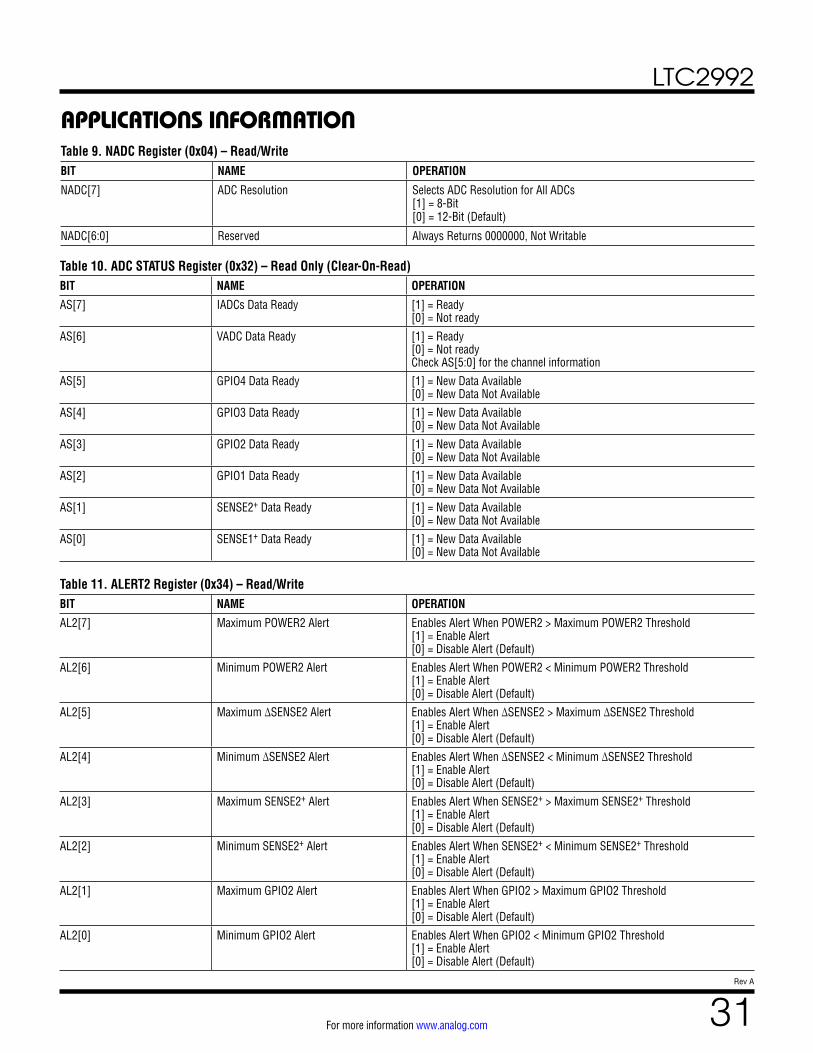
LTC2992
31Rev A
For more information www.analog.com
APPLICATIONS INFORMATIONTable 9. NADC Register (0x04) – Read/WriteBIT NAME OPERATION
NADC[7] ADC Resolution Selects ADC Resolution for All ADCs [1] = 8-Bit [0] = 12-Bit (Default)
NADC[6:0] Reserved Always Returns 0000000, Not Writable
Table 10. ADC STATUS Register (0x32) – Read Only (Clear-On-Read)BIT NAME OPERATION
AS[7] IADCs Data Ready [1] = Ready [0] = Not ready
AS[6] VADC Data Ready [1] = Ready [0] = Not ready Check AS[5:0] for the channel information
AS[5] GPIO4 Data Ready [1] = New Data Available [0] = New Data Not Available
AS[4] GPIO3 Data Ready [1] = New Data Available [0] = New Data Not Available
AS[3] GPIO2 Data Ready [1] = New Data Available [0] = New Data Not Available
AS[2] GPIO1 Data Ready [1] = New Data Available [0] = New Data Not Available
AS[1] SENSE2+ Data Ready [1] = New Data Available [0] = New Data Not Available
AS[0] SENSE1+ Data Ready [1] = New Data Available [0] = New Data Not Available
Table 11. ALERT2 Register (0x34) – Read/WriteBIT NAME OPERATION
AL2[7] Maximum POWER2 Alert Enables Alert When POWER2 > Maximum POWER2 Threshold [1] = Enable Alert [0] = Disable Alert (Default)
AL2[6] Minimum POWER2 Alert Enables Alert When POWER2 < Minimum POWER2 Threshold [1] = Enable Alert [0] = Disable Alert (Default)
AL2[5] Maximum ∆SENSE2 Alert Enables Alert When ∆SENSE2 > Maximum ∆SENSE2 Threshold [1] = Enable Alert [0] = Disable Alert (Default)
AL2[4] Minimum ∆SENSE2 Alert Enables Alert When ∆SENSE2 < Minimum ∆SENSE2 Threshold [1] = Enable Alert [0] = Disable Alert (Default)
AL2[3] Maximum SENSE2+ Alert Enables Alert When SENSE2+ > Maximum SENSE2+ Threshold [1] = Enable Alert [0] = Disable Alert (Default)
AL2[2] Minimum SENSE2+ Alert Enables Alert When SENSE2+ < Minimum SENSE2+ Threshold [1] = Enable Alert [0] = Disable Alert (Default)
AL2[1] Maximum GPIO2 Alert Enables Alert When GPIO2 > Maximum GPIO2 Threshold [1] = Enable Alert [0] = Disable Alert (Default)
AL2[0] Minimum GPIO2 Alert Enables Alert When GPIO2 < Minimum GPIO2 Threshold [1] = Enable Alert [0] = Disable Alert (Default)

LTC2992
32Rev A
For more information www.analog.com
APPLICATIONS INFORMATIONTable 12. FAULT2 Register (0x35) – Read/WriteBIT NAME OPERATIONF2[7] POWER2 Overvalue Fault POWER2 > Maximum POWER2 Threshold
[1] = POWER2 Overvalue Fault Occurred [0] = No POWER2 Overvalue Fault Occurred (Default)
F2[6] POWER2 Undervalue Fault POWER2 < Minimum POWER2 Threshold [1] = POWER2 Undervalue Fault Occurred [0] = No POWER2 Undervalue Fault Occurred (Default)
F2[5] ∆SENSE2 Overvalue Fault ∆SENSE2 > Maximum ∆SENSE2 Threshold [1] = ∆SENSE2 Overvalue Fault Occurred [0] = No ∆SENSE2 Overvalue Fault Occurred (Default)
F2[4] ∆SENSE2 Undervalue Fault ∆SENSE2 < Minimum ∆SENSE2 Threshold [1] = ∆SENSE2 Undervalue Fault Occurred [0] = No ∆SENSE2 Undervalue Fault Occurred (Default)
F2[3] SENSE2+ Overvalue Fault SENSE2+ > Maximum SENSE2+ Threshold [1] = SENSE2+ Overvalue Fault Occurred [0] = No SENSE2+ Overvalue Fault Occurred (Default)
F2[2] SENSE2+ Undervalue Fault SENSE2+ < Minimum SENSE2+ Threshold [1] = SENSE2+ Undervalue Fault Occurred [0] = No SENSE2+ Undervalue Fault Occurred (Default)
F2[1] GPIO2 Overvalue Fault GPIO2 > Maximum GPIO2 Threshold [1] = GPIO2 Overvalue Fault Occurred [0] = No GPIO2 Overvalue Fault Occurred (Default)
F2[0] GPIO2 Undervalue Fault GPIO2 < Minimum GPIO2 Threshold [1] = GPIO2 Undervalue Fault Occurred [0] = No GPIO2 Undervalue Fault Occurred (Default)
Table 13. ALERT3 Register (0x91) – Read/WriteBIT NAME OPERATIONAL3[7] Maximum GPIO3 Alert Enables Alert When GPIO3 > Maximum GPIO3 Threshold
[1] = Enable Alert [0] = Disable Alert (Default)
AL3[6] Minimum GPIO3 Alert Enables Alert When GPIO3 < Minimum GPIO3 Threshold [1] = Enable Alert [0] = Disable Alert (Default)
AL3[5] Maximum GPIO4 Alert Enables Alert When GPIO4 > Maximum GPIO4 Threshold [1] = Enable Alert [0] = Disable Alert (Default)
AL3[4] Minimum GPIO4 Alert Enables Alert When GPIO4 < Minimum GPIO4 Threshold [1] = Enable Alert [0] = Disable Alert (Default)
AL3[3] Maximum (∆SENSE1 + ∆SENSE2) Alert Enables Alert When (∆SENSE1 + ∆SENSE2) > Maximum (∆SENSE1 + ∆SENSE2) Threshold [1] = Enable Alert [0] = Disable Alert (Default)
AL3[2] Minimum (∆SENSE1 + ∆SENSE2) Alert Enables Alert When (∆SENSE1 + ∆SENSE2) < Minimum (∆SENSE1 + ∆SENSE2) Threshold [1] = Enable Alert [0] = Disable Alert (Default)
AL3[1] Maximum (POWER1 + POWER2) Alert Enables Alert When (POWER1 + POWER2) > Maximum (POWER1 + POWER2) Threshold [1] = Enable Alert [0] = Disable Alert (Default)
AL3[0] Minimum (POWER1 + POWER2) Alert Enables Alert When (POWER1 + POWER2) < Minimum (POWER1 + POWER2) Threshold [1] = Enable Alert [0] = Disable Alert (Default)
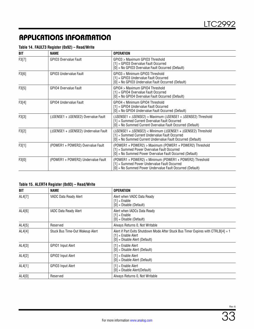
LTC2992
33Rev A
For more information www.analog.com
APPLICATIONS INFORMATIONTable 14. FAULT3 Register (0x92) – Read/WriteBIT NAME OPERATION
F3[7] GPIO3 Overvalue Fault GPIO3 > Maximum GPIO3 Threshold [1] = GPIO3 Overvalue Fault Occurred [0] = No GPIO3 Overvalue Fault Occurred (Default)
F3[6] GPIO3 Undervalue Fault GPIO3 < Minimum GPIO3 Threshold [1] = GPIO3 Undervalue Fault Occurred [0] = No GPIO3 Undervalue Fault Occurred (Default)
F3[5] GPIO4 Overvalue Fault GPIO4 > Maximum GPIO4 Threshold [1] = GPIO4 Overvalue Fault Occurred [0] = No GPIO4 Overvalue Fault Occurred (Default)
F3[4] GPIO4 Undervalue Fault GPIO4 < Minimum GPIO4 Threshold [1] = GPIO4 Undervalue Fault Occurred [0] = No GPIO4 Undervalue Fault Occurred (Default)
F3[3] (∆SENSE1 + ∆SENSE2) Overvalue Fault (∆SENSE1 + ∆SENSE2) > Maximum (∆SENSE1 + ∆SENSE2) Threshold [1] = Summed Current Overvalue Fault Occurred [0] = No Summed Current Overvalue Fault Occurred (Default)
F3[2] (∆SENSE1 + ∆SENSE2) Undervalue Fault (∆SENSE1 + ∆SENSE2) < Minimum (∆SENSE1 + ∆SENSE2) Threshold [1] = Summed Current Undervalue Fault Occurred [0] = No Summed Current Undervalue Fault Occurred (Default)
F3[1] (POWER1 + POWER2) Overvalue Fault (POWER1 + POWER2) > Maximum (POWER1 + POWER2) Threshold [1] = Summed Power Overvalue Fault Occurred [0] = No Summed Power Overvalue Fault Occurred (Default)
F3[0] (POWER1 + POWER2) Undervalue Fault (POWER1 + POWER2) < Minimum (POWER1 + POWER2) Threshold [1] = Summed Power Undervalue Fault Occurred [0] = No Summed Power Undervalue Fault Occurred (Default)
Table 15. ALERT4 Register (0x93) – Read/WriteBIT NAME OPERATION
AL4[7] VADC Data Ready Alert Alert when VADC Data Ready [1] = Enable [0] = Disable (Default)
AL4[6] IADC Data Ready Alert Alert when IADCs Data Ready [1] = Enable [0] = Disable (Default)
AL4[5] Reserved Always Returns 0, Not Writable
AL4[4] Stuck Bus Time-Out Wakeup Alert Alert if Part Exits Shutdown Mode After Stuck Bus Timer Expires with CTRLB[4] = 1 [1] = Enable Alert [0] = Disable Alert (Default)
AL4[3] GPIO1 Input Alert [1] = Enable Alert [0] = Disable Alert (Default)
AL4[2] GPIO2 Input Alert [1] = Enable Alert [0] = Disable Alert (Default)
AL4[1] GPIO3 Input Alert [1] = Enable Alert [0] = Disable Alert(Default)
AL4[0] Reserved Always Returns 0, Not Writable

LTC2992
34Rev A
For more information www.analog.com
APPLICATIONS INFORMATIONTable 16. FAULT4 Register (0x94) – Read/WriteBIT NAME OPERATION
F2[7:5] Reserved Always Returns 000, Not Writable
F4[4] Stuck Bus Time-Out Wakeup Fault With CTRLB[4] = 1 [1] = Part Exited Shutdown Mode After Stuck Bus Timer Expired [0] = No Stuck Bus Time-Out Wakeup Fault Occurred (Default)
F4[3] GPIO1 Input Fault [1] = GPIO1 Input was at Alert Level [0] = GPIO1 Input was not at Alert Level (Default) Alert Polarity is set in GIO[3] (Table 18)
F4[2] GPIO2 Input Fault [1] = GPIO2 Input was at Alert Level [0] = GPIO2 Input was not at Alert Level (Default) Alert Polarity is set in GIO[2] (Table 18)
F4[1] GPIO3 Input Fault [1] = GPIO3 Input was at Alert Level [0] = GPIO3 Input was not at Alert Level (Default) Alert Polarity is set in GIO[1] (Table 18)
F4[0] Reserved Always Returns 0, Not Writable
Table 17. GPIO STATUS Register (0x95) – Read OnlyBIT NAME OPERATION
GS[7:4] Reserved Always Returns 0000, Not Writable
GS[3] GPIO1 State [1] = GPIO1 High [0] = GPIO1 Low
GS[2] GPIO2 State [1] = GPIO2 High [0] = GPIO2 Low
GS[1] GPIO3 State [1] = GPIO3 High [0] = GPIO3 Low
GS[0] GPIO4 State [1] = GPIO4 High [0] = GPIO4 Low
Table 18. GPIO IO CONTROL Register (0x96) – Read/WriteBIT NAME OPERATION
GIO[7] GPIO1 Output [1] = Pulls Low [0] = Hi-Z (Default)
GIO[6] GPIO2 Output [1] = Pulls Low [0] = Hi-Z (Default)
GIO[5:4] GPIO3 Configuration [11] = Pulls Low when Any of the ADCs Data Becomes Ready, Resets to High by Reading ADC STATUS Register 0x32 [10] = 128µs Low Pulse when Any of the ADCs Data Becomes Available [01] = 16µs Low Pulse when Any of the ADCs Data Becomes Available [00] = General Purpose Input/Output (Default)
GIO[3] GPIO1 Alert Polarity Configuration [1] = Alert on GPIO1 Input High [0] = Alert on GPIO1 Input Low (Default)
GIO[2] GPIO2 Alert Polarity Configuration [1] = Alert on GPIO2 Input High [0] = Alert on GPIO2 Input Low (Default)
GIO[1] GPIO3 Alert Polarity Configuration [1] = Alert on GPIO3 Input High (Default) [0] = Alert on GPIO3 Input Low
GIO[0] GPIO3 Output [1] = Pulls Low (Default) [0] = Hi-Z

LTC2992
35Rev A
For more information www.analog.com
APPLICATIONS INFORMATIONTable 19. GPIO4 CONTROL Register (0x97) – Read/WriteBIT NAME OPERATION
GC[7] Alert Generated [1] = Alert Generated [0] = No Alert Generated Latched to 1 when an Alert is generated and can be cleared via I2C by writing a 0 to it or setting CTRLB[7] (Table 6) to 1
GC[6] GPIO4 Output [1] = Pulls Low [0] = Hi-Z (Default)
GC[5:0] Reserved Always Returns 000000, Not Writable
Table 20. Register Data Format – Read/Write: ADC, Min/Max ADC, Min/Max ADC Threshold, ISUM, Min/Max ISUM, Min/Max ISUM Threshold12-Bit Mode:
BIT(7) BIT(6) BIT(5) BIT(4) BIT(3) BIT(2) BIT(1) BIT(0)
MSB Register Data(11) Data(10) Data(9) Data(8) Data(7) Data(6) Data(5) Data(4)
LSB Register Data(3) Data(2) Data(1) Data(0) 0 0 0 0
8-Bit Mode:
BIT(7) BIT(6) BIT(5) BIT(4) BIT(3) BIT(2) BIT(1) BIT(0)
MSB2 Register Data(15) Data(14) Data(13) Data(12) Data(11) Data(10) Data(9) Data(8)
MSB1 Register Data(7) Data(6) Data(5) Data(4) Data(3) Data(2) Data(1) Data(0)
LSB Register 0 0 0 0 0 0 0 0
Table 21. Register Data Format – Read/Write: Power, Min/Max Power, Min/Max Power Threshold, PSUM, Min/Max PSUM, Min/Max PSUM Threshold12-Bit Mode:
BIT(7) BIT(6) BIT(5) BIT(4) BIT(3) BIT(2) BIT(1) BIT(0)
MSB2 Register Data(23) Data(22) Data(21) Data(20) Data(19) Data(18) Data(17) Data(16)
MSB1 Register Data(15) Data(14) Data(13) Data(12) Data(11) Data(10) Data(9) Data(8)
LSB Register Data(7) Data(6) Data(5) Data(4) Data(3) Data(2) Data(1) Data(0)
8-Bit Mode:
BIT(7) BIT(6) BIT(5) BIT(4) BIT(3) BIT(2) BIT(1) BIT(0)
MSB Register Data(7) Data(6) Data(5) Data(4) Data(3) Data(2) Data(1) Data(0)
LSB Register 0 0 0 0 0 0 0 0

LTC2992
36Rev A
For more information www.analog.com
TYPICAL APPLICATIONS
–48V Redundant Feed with Transient Protection to 200V (1.5kHz I2C Interface)
High Side and Low Side Current Sensing on a Wide Range Supply
RSENSE10.01Ω
RSENSE20.01Ω
2992 TA03
ADR1
GND
LTC2992
VDD
INTVCC
ADR0
SDAO
SCL
SDAI
C11µF
R140.2k1%
GPIO1
GPIO2
GPIO4
GPIO3
ALERT
GP OUTPUT
I2CINTERFACEVIN
7V TO100V
SENSE2– SENSE2+
SENSE1+ SENSE1–
R319.1k1%
VISHAYNTCS0402E3104*HT
100k AT 25°C1%
R210k1%
R420k1%
+
–LOAD
5A
T(°C) = 41.51 • ( – 0.1233), 20°C < T < 60°CE PE ECODEGPIOCODEGPIO2
GPIO2
GNDGPIO4
SDAO
ADR0
ADR1
SDAI
SCL
LTC2992-1
VDD INTVCC
GPIO1
GPIO3TEMPERATURESENSOR
SENSE1– SENSE1+SENSE2– SENSE2+
RSENSE10.01Ω
RSENSE20.01Ω
MBR20200*
MBR20200*
MOCD207M
MOCD207M
VOUT5A
2992 TA02
ALERT
R31k
R40.51k
R12k
R90.51k
R100.51k
R112k
R122k
R1310k VDD
3.3V
INT
SDA
SCL
GND
µP
C11µF
VIN1–48V
VIN2–48V
R820k
R720k
R61M
RTN1
RTN2
R51M
*APPROPRIATELY SIZED HEAT SINK IS REQUIRED
RSHUNT29.1k1W
RSHUNT19.1k1W
R22k
MBR20200*
MBR20200*
R14100Ω
Q1, PZTA42
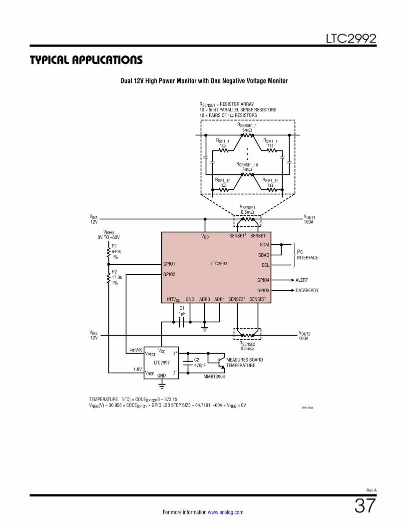
LTC2992
37Rev A
For more information www.analog.com
TYPICAL APPLICATIONS
Dual 12V High Power Monitor with One Negative Voltage Monitor
RSENSE10.5mΩ
RSENSE20.5mΩ
2992 TA04
1.8V
4mV/K
LTC2992
VDD
INTVCC
SDAO
SCL
SDAI
C11µF
GPIO1
GPIO2GPIO4
GPIO3
ADR0 ADR1GND
ALERT
DATAREADY
I2CINTERFACE
SENSE2+ SENSE2–
SENSE1+ SENSE1–VNEG0V TO –60V
VIN212V
VOUT2100A
VIN112V
VOUT1100A
C2470pF
MMBT3904
MEASURES BOARDTEMPERATURE
D+
D–
VPTATVCC
VREF GND
TEMPERATURE
LTC2997
R1640k1%
R217.8k1%
RSENSE1_105mΩ
RSP1_101Ω
RSM1_101Ω
RSENSE1_15mΩ
RSP1_11Ω
RSM1_11Ω
• •
•
T(°C) = CODEGPIO2/8 – 273.15VNEG(V) = 36.955 × CODEGPIO1 × GPIO LSB STEP SIZE – 64.7191, –60V < VNEG < 0V
RSENSE1 = RESISTOR ARRAY10 × 5mΩ PARALLEL SENSE RESISTORS10 × PAIRS OF 1Ω RESISTORS
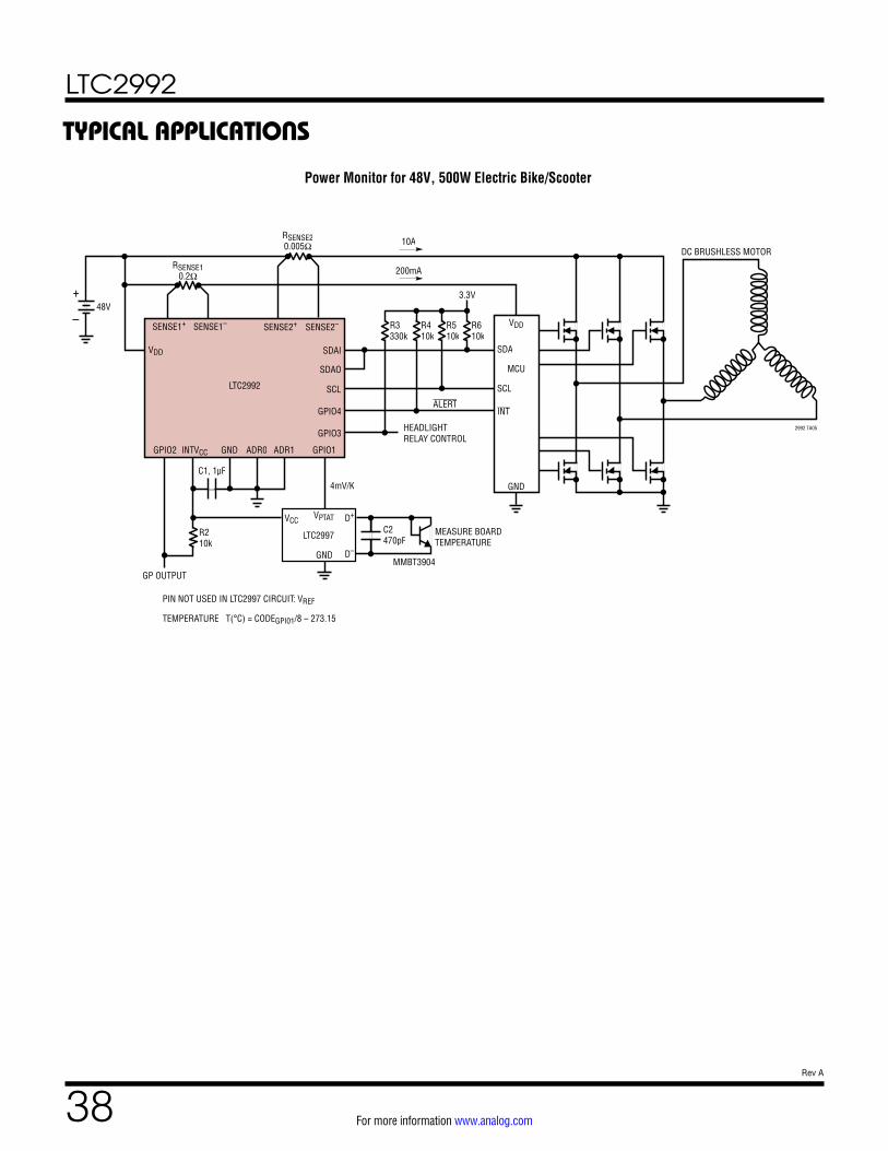
LTC2992
38Rev A
For more information www.analog.com
TYPICAL APPLICATIONS
Power Monitor for 48V, 500W Electric Bike/Scooter
GPIO1GPIO2 ADR1ADR0GNDINTVCC
GP OUTPUT
GPIO4
GPIO3
SCL
SDAO
SDAI
LTC2992
VDD
48V
SENSE2+ SENSE2–SENSE1+
RSENSE10.2Ω
RSENSE20.005Ω
SENSE1– R3330k
R410k
R510k
VDD
MCU
GND
3.3V
10A
INTALERT
SCL
HEADLIGHTRELAY CONTROL
SDA
PIN NOT USED IN LTC2997 CIRCUIT: VREF
TEMPERATURE T(°C) = CODEGPI01/8 – 273.15
2992 TA05
4mV/K
MEASURE BOARDTEMPERATURE
DC BRUSHLESS MOTOR
MMBT3904
R610k
C1, 1µF
GND
LTC2997
D+
D–
VCCVPTAT
R210k
C2470pF
200mA
+
–

LTC2992
39Rev A
For more information www.analog.com
TYPICAL APPLICATIONS
Four Quadrant Power Monitor (10kHz I2C Interface)
GPIO2
GPIO4
ADR1
ADR0
GND
SDAO
SDAI
SCL
LTC2992-1
VDD
NC
NC
INTVCC
GPIO1
GPIO3
VIN–95V TO
100V
ORGND(GND PIN
OF LTC2992-1)
SENSE2– SENSE1+SENSE1– SENSE2+
MOCD207M
MOCD207M
2992 TA06
ALERT
R633k
R70.82k
R84.7k
R100.47k
R110.47k
R122k
R132k
R1410k VDD
3.3V
INT
SDA
SCL
GND
µP
R17100k
R16100k
R41M
SEPARATE5V SUPPLY
TEMPERATURESENSOR
R94.7k
PIN NOT USED IN LTC4371 CIRCUIT: FAULTB
NC: NO CONNECT
IF CODEGPIO1 > CODEGPIO2, MEASURED VIN = –[CODEGPIO1 × GPIO LSB STEP SIZE × 51]IF CODEGPIO1 < CODEGPIO2, MEASURED VIN = CODEGPIO2 × GPIO LSB STEP SIZE × 51VDS,Q2, VDS,Q3 ARE DRAIN TO SOURCE VOLTAGE OF Q2 AND Q3VRSENSE IS VOLTAGE ACROSS RSENSE
*MAX EMITTER-BASE BREAKDOWN VOLTAGE OF Q4, Q5 SHOULD BE LESS THAN 7V
C11µF ORGND
Q4*MMBT2222L
Q1PZTA42
SB
LTC4371
SA
GA
DA
GB
VOUT5A
DB
VSS VZ VDD
C31nF
R15, 10k
C21nF
Q3BSP297
Q2BSP297
RSENSE0.01Ω
Q5*MMBT2222L
+
–
R11M
R320k
R220k
|VIN| – |VRSENSE|–|VDS,Q2|×
51
1
GPIO LSB STEP SIZE
|VIN| – |VDS,Q3|×
51
1
GPIO LSB STEP SIZE
CODEGPIO1 =
CODEGPIO2 =

LTC2992
40Rev A
For more information www.analog.com
TYPICAL APPLICATIONS
Power Efficiency Meter
CA0.1µF
LTC2992
SDAI
SDAO
SCL
SENSE2–
SENSE2+
INTVCC
ADR1
ADR0
GND
GPIO1
GPIO4
GPIO2 GPIO3
VDD
SENSE1+
SENSE1–
RPU4100k
ALERT
LTC3895
VINRUN
MODE
ILIM
TG
BOOST
SW
BG
SENSE+
SENSE–
VFB
ITHDRVCC
2992 TA07
DRVSET
DRVUV
RPU3100k
RB, 140k
RPU2100k
OVLO
PINS NOT USED IN LTC3895 CIRCUIT:CLKOUT, PLLIN, PHASMD, PGOOD, VPRG
MTOP, MBOT: BSC520N15NS3GDEXT: DIODES INC. SMAZ12-13-FL1: WURTH 7443633300COUTA: SUNCON 35CE68LX
NDRV
INTVCC
CRUMP_EN
SS
EXTVCC
CB0.1µF L1, 33µH
FREQ
GND
GND
GND
GND
CSNS1nF
MBOT
MTOP×2
CITHB100pF
CITHA4.7nF
RFREQ30.1k
RDRV80.6k
RITH10k
RA10k
CEXT1µF
RPU1100k
CINA100µF
RSENSE110mΩ
RSENSE26mΩ
VIN14V TO 100V
I2CINTERFACE
+ CINB0.47µF×4
CINTVCC0.1µF
CDRVCC4.7µF
CSS0.1µF
COUTA150µF×2
VOUT12V5A
+COUTB22µF

LTC2992
41Rev A
For more information www.analog.com
TYPICAL APPLICATIONS
Bidirectional 30V to 300V High Side Power Monitor
GPIO2
NST30010MXV6
GPIO4
GPIO3GND
LTC2992GPIO1
SENSE1– SENSE2+SENSE2– SENSE1+
2992 TA08
ADR0
ADR1
SDAO
SDAI
SCL
INTVCC
VDD
ADUM1251
VDD2
SDA2
SCL2
GND2
VDD1
SDA1
SCL1
GND1
USE GPIO TO MEASURE INPUT VOLTAGESEE TABLE 5*DDZ9689, DIODES INC.
RSENSE0.01Ω
VIN
R11100Ω
Q2MMBT6520L
Q12N3904
M3BSP135
R12374k
R13374k
R610k
R510k
M1BSP135
Q32N3904
FAN ONOUTPUT
ALERT
R35k
C20.1µF
VOUT5A
R42k
R72k
R81k
R91k
R1010k VDD
µP
3.3V
C10.1µF
R12k
Z1*5.1V
R112k
R25.1k
SDA
SCL
INT
GND
FODM217C
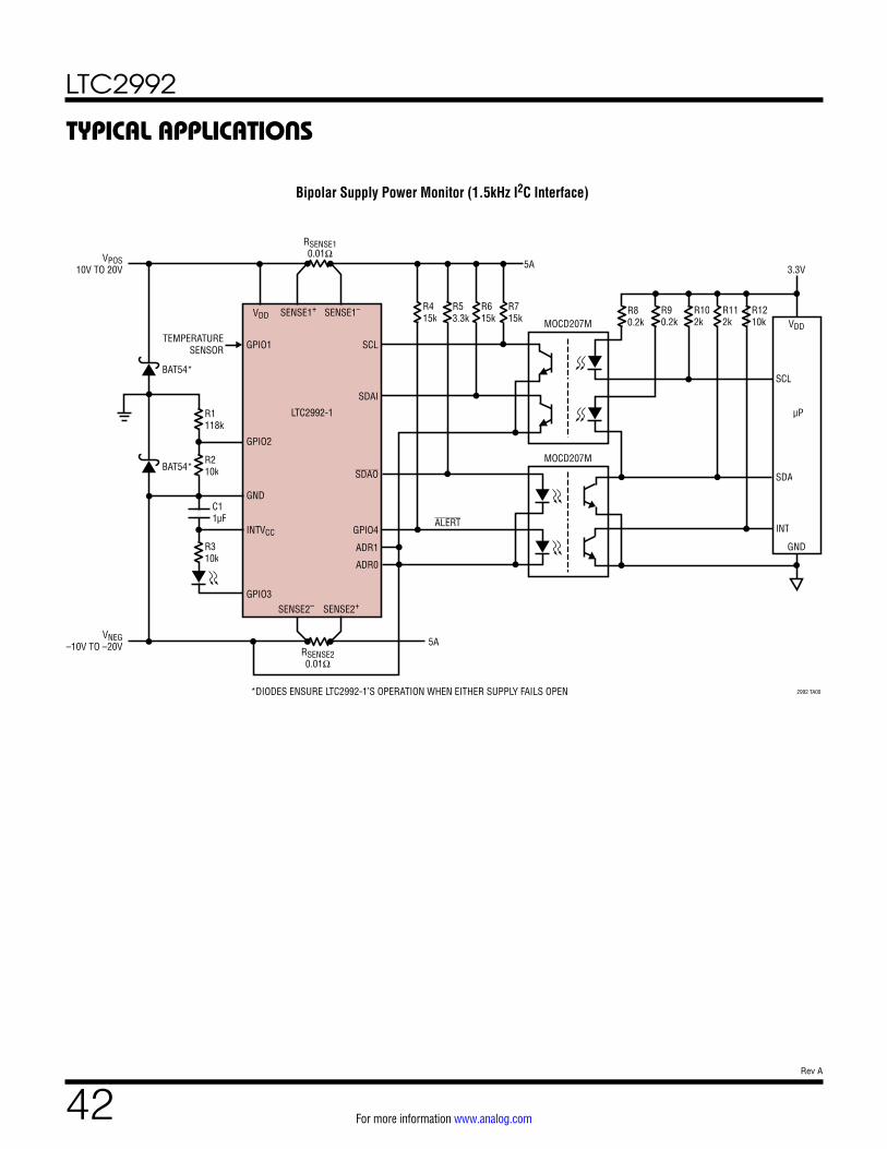
LTC2992
42Rev A
For more information www.analog.com
TYPICAL APPLICATIONS
Bipolar Supply Power Monitor (1.5kHz I2C Interface)
GPIO2
GND
INTVCC
GPIO3
GPIO4
ADR0
ADR1
SDAO
SDAI
SCL
LTC2992-1
VDD
GPIO1
SENSE2– SENSE2+
SENSE1+ SENSE1–
MOCD207M
MOCD207M
2992 TA09
ALERT
R415k
R53.3k
R615k
R80.2k
R90.2k
R102k
R112k
R1210k VDD
3.3V
INT
SDA
SCL
GND
µP
VNEG–10V TO –20V
VPOS10V TO 20V
5A
TEMPERATURESENSOR
*DIODES ENSURE LTC2992-1’S OPERATION WHEN EITHER SUPPLY FAILS OPEN
R715k
5A
BAT54*
BAT54*
RSENSE20.01Ω
RSENSE10.01Ω
C11µF
R1118k
R210k
R310k

LTC2992
43Rev A
For more information www.analog.com
PACKAGE DESCRIPTIONPlease refer to http://www.linear.com/product/LTC2992#packaging for the most recent package drawings.
3.00 ±0.10(2 SIDES)
4.00 ±0.10(2 SIDES)
NOTE:1. DRAWING PROPOSED TO BE MADE VARIATION OF VERSION (WGED-3) IN JEDEC PACKAGE OUTLINE MO-2292. DRAWING NOT TO SCALE 3. ALL DIMENSIONS ARE IN MILLIMETERS4. DIMENSIONS OF EXPOSED PAD ON BOTTOM OF PACKAGE DO NOT INCLUDE MOLD FLASH. MOLD FLASH, IF PRESENT, SHALL NOT EXCEED 0.15mm ON ANY SIDE5. EXPOSED PAD SHALL BE SOLDER PLATED6. SHADED AREA IS ONLY A REFERENCE FOR PIN 1 LOCATION ON THE TOP AND BOTTOM OF PACKAGE
0.40 ±0.10
BOTTOM VIEW—EXPOSED PAD
1.70 ±0.10
0.75 ±0.05
R = 0.115TYP
R = 0.05TYP
3.15 REF
1.70 ±0.05
18
169
PIN 1TOP MARK
(SEE NOTE 6)
0.200 REF
0.00 – 0.05
(DE16) DFN 0806 REV Ø
PIN 1 NOTCHR = 0.20 OR0.35 × 45°CHAMFER
3.15 REF
RECOMMENDED SOLDER PAD PITCH AND DIMENSIONSAPPLY SOLDER MASK TO AREAS THAT ARE NOT SOLDERED
2.20 ±0.05
0.70 ±0.05
3.60 ±0.05
PACKAGEOUTLINE
0.25 ±0.05
3.30 ±0.05
3.30 ±0.10
0.45 BSC
0.23 ±0.050.45 BSC
DE Package16-Lead Plastic DFN (4mm × 3mm)
(Reference LTC DWG # 05-08-1732 Rev Ø)

LTC2992
44Rev A
For more information www.analog.com
PACKAGE DESCRIPTIONPlease refer to http://www.linear.com/product/LTC2992#packaging for the most recent package drawings.
MSOP (MS16) 0213 REV A
0.53 0.152(.021 .006)
SEATINGPLANE
0.18(.007)
1.10(.043)MAX
0.17 – 0.27(.007 – .011)
TYP
0.86(.034)REF
0.50(.0197)
BSC
16151413121110
1 2 3 4 5 6 7 8
9
NOTE:1. DIMENSIONS IN MILLIMETER/(INCH)2. DRAWING NOT TO SCALE3. DIMENSION DOES NOT INCLUDE MOLD FLASH, PROTRUSIONS OR GATE BURRS. MOLD FLASH, PROTRUSIONS OR GATE BURRS SHALL NOT EXCEED 0.152mm (.006") PER SIDE4. DIMENSION DOES NOT INCLUDE INTERLEAD FLASH OR PROTRUSIONS. INTERLEAD FLASH OR PROTRUSIONS SHALL NOT EXCEED 0.152mm (.006") PER SIDE5. LEAD COPLANARITY (BOTTOM OF LEADS AFTER FORMING) SHALL BE 0.102mm (.004") MAX
0.254(.010) 0 – 6 TYP
DETAIL “A”
DETAIL “A”
GAUGE PLANE
5.10(.201)MIN
3.20 – 3.45(.126 – .136)
0.889 0.127(.035 .005)
RECOMMENDED SOLDER PAD LAYOUT
0.305 0.038(.0120 .0015)
TYP
0.50(.0197)
BSC
4.039 0.102(.159 .004)
(NOTE 3)
0.1016 0.0508(.004 .002)
3.00 0.102(.118 .004)
(NOTE 4)
0.280 0.076(.011 .003)
REF
4.90 0.152(.193 .006)
MS Package16-Lead Plastic MSOP
(Reference LTC DWG # 05-08-1669 Rev A)

LTC2992
45Rev A
For more information www.analog.com
Information furnished by Analog Devices is believed to be accurate and reliable. However, no responsibility is assumed by Analog Devices for its use, nor for any infringements of patents or other rights of third parties that may result from its use. Specifications subject to change without notice. No license is granted by implication or otherwise under any patent or patent rights of Analog Devices.
REVISION HISTORYREV DATE DESCRIPTION PAGE NUMBER
A 04/18 Corrected DATA Pointers in Figure 7 19

LTC2992
46Rev A
For more information www.analog.com
D16849-0-4/18(A)www.analog.com
ANALOG DEVICES, INC. 2017-2018
RELATED PARTS
TYPICAL APPLICATION
PART NUMBER DESCRIPTION COMMENTS
LT®2940 Power and Current Monitor 4-Quadrant Multiplication, ±5% Power Accuracy, 4V to 80V Operation
LTC2941 I2C Battery Gas Gauge 2.7V to 5.5V Operation, 1% Charge Accuracy
LTC2942 I2C Battery Gas Gauge 2.7V to 5.5V Operation, 1% Charge, Voltage and Temperature
LTC2943 High Voltage Battery Gas Gauge 3.6V to 20V Operation, 1% Charge, Voltage, Current and Temperature
LTC2945 Wide Range I2C Power Monitor 0V to 80V Operation, 12-Bit ADC with ±0.75% TUE
LTC2947 Power/Energy Monitor with Integrated Sense Resistor ±30A Current Range with 9mA Offset
LTC2990 Quad I2C Temperature, Voltage and Current Monitor 3V to 5.5V Operation, 14-Bit ADC
LTC4150 Coulomb Counter/Battery Gas Gauge 2.7V to 8.5V Operation, Voltage-to-Frequency Converter
LTC4151 High Voltage I2C Current and Voltage Monitor 7V to 80V Operation, 12-Bit Resolution with ±1.25% TUE
LTC4215 Single Channel, Hot Swap Controller with I2C Monitoring
8-Bit ADC, Adjustable Current Limit and Inrush, 2.9V to 15V Operation
LTC4222 Dual Channel, Hot Swap Controller with I2C Monitoring
10-Bit ADC, Adjustable Current Limit and Inrush, 2.9V to 29V Operation
LTC4260 Positive High Voltage Hot Swap Controller with I2C Monitoring
8-Bit ADC, Adjustable Current Limit and Inrush, 8.5V to 80V Operation
LTC4261 Negative High Voltage Hot Swap Controller with I2C Monitoring
10-Bit ADC, Floating Topology, Adjustable Inrush
Bidirectional Wide Range Power Monitor
VDD
LTC2992
SDAI
SDAO
SCL
GPIO1
GPIO2
GPIO3
VIN3V TO 100V
I2CINTERFACE
ALERT
2992 TA10
SENSE1– SENSE2+SENSE2– SENSE1+
RSENSE0.01Ω
0.1μF
ADR0 ADR1GNDINTVCC
GPIO4
BOARDTEMPERATURE
µPTEMPERATURE
DATAREADY
VOUT


![A Reinforcement Learning Based QAM/PSK Symbol Synchronizer · M. Matta et al.: A Reinforcement Learning Based QAM/PSK Symbol Synchronizer parameter spaces [25]. Moreover, the inference](https://static.fdocuments.us/doc/165x107/5f574e39556bdd57e05851bb/a-reinforcement-learning-based-qampsk-symbol-synchronizer-m-matta-et-al-a-reinforcement.jpg)