
LTC2635 (Rev D) - analog.com · D D RR RR RR RR D D VD R VCC VR VOUTC R SWITCH RR I2 RACE DD I2C...
32
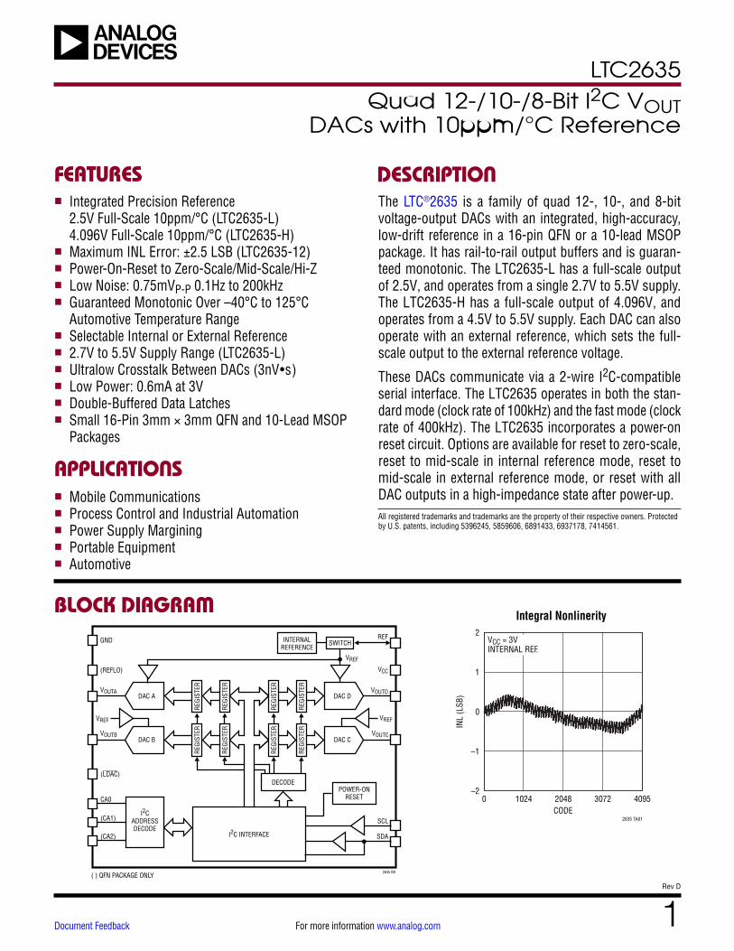
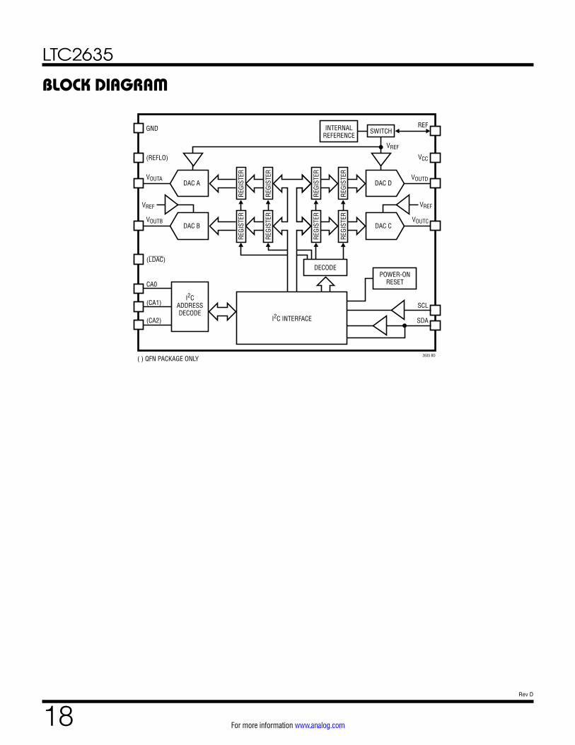
LTC2635 1 Rev D For more information www.analog.com Document Feedback BLOCK DIAGRAM DESCRIPTION Quad 12-/10-/8-Bit I 2 C V OUT DACs with 10ppm/°C Reference The LTC ® 2635 is a family of quad 12-, 10-, and 8-bit voltage-output DACs with an integrated, high-accuracy, low-drift reference in a 16-pin QFN or a 10-lead MSOP package. It has rail-to-rail output buffers and is guaran- teed monotonic. The LTC2635-L has a full-scale output of 2.5V, and operates from a single 2.7V to 5.5V supply. The LTC2635-H has a full-scale output of 4.096V, and operates from a 4.5V to 5.5V supply. Each DAC can also operate with an external reference, which sets the full- scale output to the external reference voltage. These DACs communicate via a 2-wire I 2 C-compatible serial interface. The LTC2635 operates in both the stan- dard mode (clock rate of 100kHz) and the fast mode (clock rate of 400kHz). The LTC2635 incorporates a power-on reset circuit. Options are available for reset to zero-scale, reset to mid-scale in internal reference mode, reset to mid-scale in external reference mode, or reset with all DAC outputs in a high-impedance state after power-up. Integral Nonlinerity FEATURES APPLICATIONS n Integrated Precision Reference 2.5V Full-Scale 10ppm/°C (LTC2635-L) 4.096V Full-Scale 10ppm/°C (LTC2635-H) n Maximum INL Error: ±2.5 LSB (LTC2635-12) n Power-On-Reset to Zero-Scale/Mid-Scale/Hi-Z n Low Noise: 0.75mV P-P 0.1Hz to 200kHz n Guaranteed Monotonic Over –40°C to 125°C Automotive Temperature Range n Selectable Internal or External Reference n 2.7V to 5.5V Supply Range (LTC2635-L) n Ultralow Crosstalk Between DACs (3nV•s) n Low Power: 0.6mA at 3V n Double-Buffered Data Latches n Small 16-Pin 3mm × 3mm QFN and 10-Lead MSOP Packages n Mobile Communications n Process Control and Industrial Automation n Power Supply Margining n Portable Equipment n Automotive REGISTER REGISTER REGISTER REGISTER DAC A V OUTA (REFLO) (LDAC) CA0 (CA1) (CA2) ( ) QFN PACKAGE ONLY GND V OUTB V REF DAC D REGISTER REGISTER REGISTER REGISTER DAC B DAC C V REF V OUTD REF V CC V REF V OUTC SWITCH INTERNAL REFERENCE I 2 C INTERFACE DECODE I 2 C ADDRESS DECODE POWER-ON RESET SCL SDA 2635 BD All registered trademarks and trademarks are the property of their respective owners. Protected by U.S. patents, including 5396245, 5859606, 6891433, 6937178, 7414561. CODE 0 INL (LSB) 2 1 0 –1 –2 1024 3072 2635 TA01 4095 2048 V CC = 3V INTERNAL REF.
-
Upload
truongliem -
Category
Documents
-
view
223 -
download
0
Transcript of LTC2635 (Rev D) - analog.com · D D RR RR RR RR D D VD R VCC VR VOUTC R SWITCH RR I2 RACE DD I2C...
LTC2635
1Rev D
For more information www.analog.comDocument Feedback
BLOCK DIAGRAM
DESCRIPTION
Quad 12-/10-/8-Bit I2C VOUT DACs with 10ppm/°C Reference
The LTC®2635 is a family of quad 12-, 10-, and 8-bit voltage-output DACs with an integrated, high-accuracy, low-drift reference in a 16-pin QFN or a 10-lead MSOP package. It has rail-to-rail output buffers and is guaran-teed monotonic. The LTC2635-L has a full-scale output of 2.5V, and operates from a single 2.7V to 5.5V supply. The LTC2635-H has a full-scale output of 4.096V, and operates from a 4.5V to 5.5V supply. Each DAC can also operate with an external reference, which sets the full-scale output to the external reference voltage.
These DACs communicate via a 2-wire I2C-compatible serial interface. The LTC2635 operates in both the stan-dard mode (clock rate of 100kHz) and the fast mode (clock rate of 400kHz). The LTC2635 incorporates a power-on reset circuit. Options are available for reset to zero-scale, reset to mid-scale in internal reference mode, reset to mid-scale in external reference mode, or reset with all DAC outputs in a high-impedance state after power-up.
Integral Nonlinerity
FEATURES
APPLICATIONS
n Integrated Precision Reference 2.5V Full-Scale 10ppm/°C (LTC2635-L) 4.096V Full-Scale 10ppm/°C (LTC2635-H)n Maximum INL Error: ±2.5 LSB (LTC2635-12)n Power-On-Reset to Zero-Scale/Mid-Scale/Hi-Zn Low Noise: 0.75mVP-P 0.1Hz to 200kHzn Guaranteed Monotonic Over –40°C to 125°C
Automotive Temperature Rangen Selectable Internal or External Referencen 2.7V to 5.5V Supply Range (LTC2635-L)n Ultralow Crosstalk Between DACs (3nV•s)n Low Power: 0.6mA at 3Vn Double-Buffered Data Latchesn Small 16-Pin 3mm × 3mm QFN and 10-Lead MSOP
Packages
n Mobile Communicationsn Process Control and Industrial Automationn Power Supply Marginingn Portable Equipmentn Automotive
REGI
STER
REGI
STER
REGI
STER
REGI
STER
DAC AVOUTA
(REFLO)
(LDAC)
CA0
(CA1)
(CA2)
( ) QFN PACKAGE ONLY
GND
VOUTB
VREF
DAC D
REGI
STER
REGI
STER
REGI
STER
REGI
STER
DAC B DAC C
VREF
VOUTD
REF
VCC
VREF
VOUTC
SWITCHINTERNALREFERENCE
I2C INTERFACE
DECODE
I2CADDRESSDECODE
POWER-ONRESET
SCL
SDA
2635 BD
All registered trademarks and trademarks are the property of their respective owners. Protected by U.S. patents, including 5396245, 5859606, 6891433, 6937178, 7414561.
CODE0
INL
(LSB
)
2
1
0
–1
–21024 3072
2635 TA01
40952048
VCC = 3VINTERNAL REF.
LTC2635
2Rev D
For more information www.analog.com
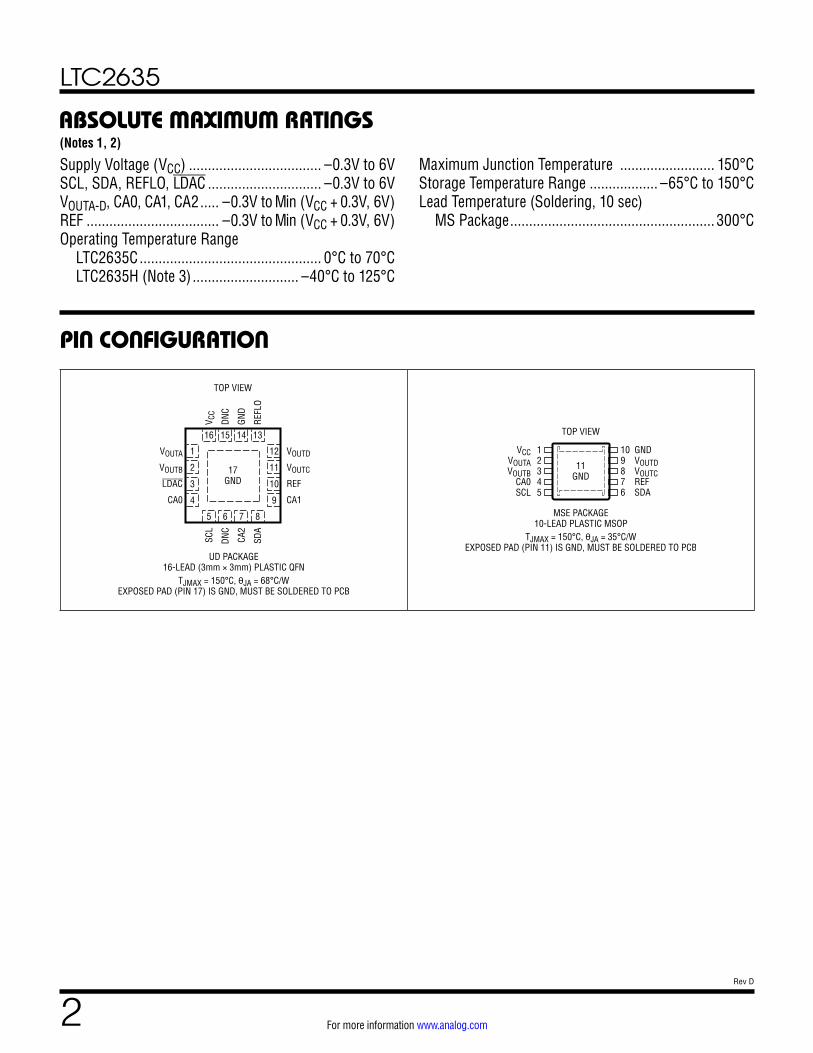
PIN CONFIGURATION
ABSOLUTE MAXIMUM RATINGS
Supply Voltage (VCC) ................................... –0.3V to 6VSCL, SDA, REFLO, LDAC .............................. –0.3V to 6VVOUTA-D, CA0, CA1, CA2 ..... –0.3V to Min (VCC + 0.3V, 6V)REF ................................... –0.3V to Min (VCC + 0.3V, 6V)Operating Temperature Range LTC2635C ................................................ 0°C to 70°C LTC2635H (Note 3) ............................ –40°C to 125°C
(Notes 1, 2)
Maximum Junction Temperature ......................... 150°CStorage Temperature Range .................. –65°C to 150°CLead Temperature (Soldering, 10 sec) MS Package ...................................................... 300°C
16 15 14 13
5 6 7 8
TOP VIEW
17GND
UD PACKAGE16-LEAD (3mm × 3mm) PLASTIC QFN
TJMAX = 150°C, θJA = 68°C/WEXPOSED PAD (PIN 17) IS GND, MUST BE SOLDERED TO PCB
9
10
11
12
4
3
2
1VOUTA
VOUTB
LDAC
CA0
VOUTD
VOUTC
REF
CA1
V CC
DNC
GND
REFL
O
SCL
DNC
CA2
SDA
12345
VCCVOUTAVOUTB
CA0SCL
109876
GNDVOUTDVOUTCREFSDA
TOP VIEW
11GND
MSE PACKAGE10-LEAD PLASTIC MSOP
TJMAX = 150°C, θJA = 35°C/WEXPOSED PAD (PIN 11) IS GND, MUST BE SOLDERED TO PCB
LTC2635
3Rev D
For more information www.analog.com
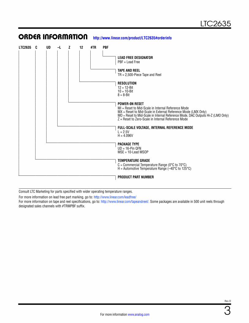
http://www.linear.com/product/LTC2635#orderinfoORDER INFORMATIONLTC2635 C UD –L Z 12 #TR PBF
LEAD FREE DESIGNATORPBF = Lead Free
TAPE AND REELTR = 2,500-Piece Tape and Reel
RESOLUTION12 = 12-Bit 10 = 10-Bit 8 = 8-Bit
POWER-0N RESETMI = Reset to Mid-Scale in Internal Reference Mode MX = Reset to Mid-Scale in External Reference Mode (LMX Only) MO = Reset to Mid-Scale in Internal Reference Mode, DAC Outputs Hi-Z (LMO Only) Z = Reset to Zero-Scale in Internal Reference Mode
FULL-SCALE VOLTAGE, INTERNAL REFERENCE MODEL = 2.5V H = 4.096V
PACKAGE TYPEUD = 16-Pin QFN MSE = 10-Lead MSOP
TEMPERATURE GRADEC = Commercial Temperature Range (0°C to 70°C) H = Automotive Temperature Range (–40°C to 125°C)
PRODUCT PART NUMBER
Consult LTC Marketing for parts specified with wider operating temperature ranges.For more information on lead free part marking, go to: http://www.linear.com/leadfree/ For more information on tape and reel specifications, go to: http://www.linear.com/tapeandreel/. Some packages are available in 500 unit reels through designated sales channels with #TRMPBF suffix.
LTC2635
4Rev D
For more information www.analog.com
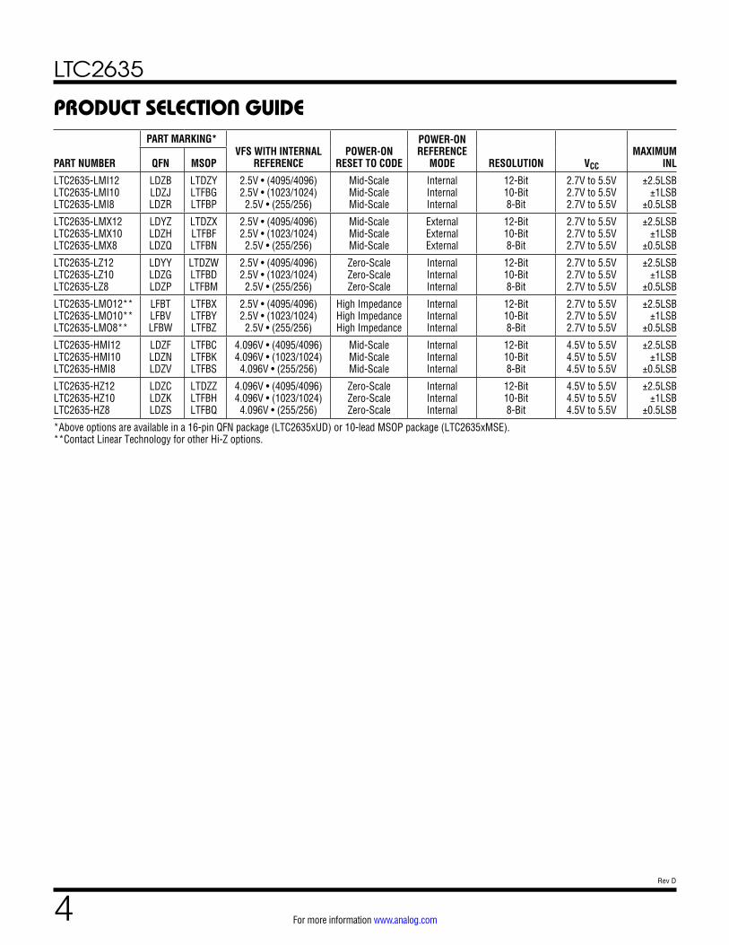
PRODUCT SELECTION GUIDE
PART NUMBER
PART MARKING*VFS WITH INTERNAL
REFERENCEPOWER-ON
RESET TO CODE
POWER-ON REFERENCE
MODE RESOLUTION VCC
MAXIMUM INLQFN MSOP
LTC2635-LMI12 LTC2635-LMI10 LTC2635-LMI8
LDZB LDZJ LDZR
LTDZY LTFBG LTFBP
2.5V • (4095/4096) 2.5V • (1023/1024)
2.5V • (255/256)
Mid-Scale Mid-Scale Mid-Scale
Internal Internal Internal
12-Bit 10-Bit 8-Bit
2.7V to 5.5V 2.7V to 5.5V 2.7V to 5.5V
±2.5LSB ±1LSB
±0.5LSB
LTC2635-LMX12 LTC2635-LMX10 LTC2635-LMX8
LDYZ LDZH LDZQ
LTDZX LTFBF LTFBN
2.5V • (4095/4096) 2.5V • (1023/1024)
2.5V • (255/256)
Mid-Scale Mid-Scale Mid-Scale
External External External
12-Bit 10-Bit 8-Bit
2.7V to 5.5V 2.7V to 5.5V 2.7V to 5.5V
±2.5LSB ±1LSB
±0.5LSB
LTC2635-LZ12 LTC2635-LZ10 LTC2635-LZ8
LDYY LDZG LDZP
LTDZW LTFBD LTFBM
2.5V • (4095/4096) 2.5V • (1023/1024)
2.5V • (255/256)
Zero-Scale Zero-Scale Zero-Scale
Internal Internal Internal
12-Bit 10-Bit 8-Bit
2.7V to 5.5V 2.7V to 5.5V 2.7V to 5.5V
±2.5LSB ±1LSB
±0.5LSB
LTC2635-LMO12** LTC2635-LMO10** LTC2635-LMO8**
LFBT LFBV LFBW
LTFBX LTFBY LTFBZ
2.5V • (4095/4096) 2.5V • (1023/1024)
2.5V • (255/256)
High Impedance High Impedance High Impedance
Internal Internal Internal
12-Bit 10-Bit 8-Bit
2.7V to 5.5V 2.7V to 5.5V 2.7V to 5.5V
±2.5LSB ±1LSB
±0.5LSB
LTC2635-HMI12 LTC2635-HMI10 LTC2635-HMI8
LDZF LDZN LDZV
LTFBC LTFBK LTFBS
4.096V • (4095/4096) 4.096V • (1023/1024) 4.096V • (255/256)
Mid-Scale Mid-Scale Mid-Scale
Internal Internal Internal
12-Bit 10-Bit 8-Bit
4.5V to 5.5V 4.5V to 5.5V 4.5V to 5.5V
±2.5LSB ±1LSB
±0.5LSB
LTC2635-HZ12 LTC2635-HZ10 LTC2635-HZ8
LDZC LDZK LDZS
LTDZZ LTFBH LTFBQ
4.096V • (4095/4096) 4.096V • (1023/1024) 4.096V • (255/256)
Zero-Scale Zero-Scale Zero-Scale
Internal Internal Internal
12-Bit 10-Bit 8-Bit
4.5V to 5.5V 4.5V to 5.5V 4.5V to 5.5V
±2.5LSB ±1LSB
±0.5LSB
*Above options are available in a 16-pin QFN package (LTC2635xUD) or 10-lead MSOP package (LTC2635xMSE). **Contact Linear Technology for other Hi-Z options.
LTC2635
5Rev D
For more information www.analog.com
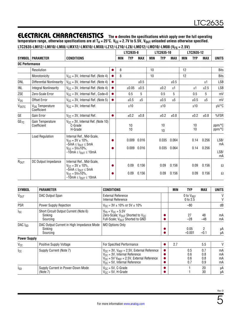
ELECTRICAL CHARACTERISTICS The l denotes the specifications which apply over the full operating temperature range, otherwise specifications are at TA = 25°C. VCC = 2.7V to 5.5V, VOUT unloaded unless otherwise specified.LTC2635-LMI12/-LMI10/-LMI8/-LMX12/-LMX10/-LMX8/-LZ12/-LZ10/-LZ8/-LMO12/-LMO10/-LM08 (VFS = 2.5V)
SYMBOL PARAMETER CONDITIONS
LTC2635-8 LTC2635-10 LTC2635-12
UNITSMIN TYP MAX MIN TYP MAX MIN TYP MAX
DC Performance
Resolution l 8 10 12 Bits
Monotonicity VCC = 3V, Internal Ref. (Note 4) l 8 10 12 Bits
DNL Differential Nonlinearity VCC = 3V, Internal Ref. (Note 4) l ±0.5 ±0.5 ±1 LSB
INL Integral Nonlinearity VCC = 3V, Internal Ref. (Note 4) l ±0.05 ±0.5 ±0.2 ±1 ±1 ±2.5 LSB
ZSE Zero-Scale Error VCC = 3V, Internal Ref., Code=0 l 0.5 5 0.5 5 0.5 5 mV
VOS Offset Error VCC = 3V, Internal Ref. (Note 5) l ±0.5 ±5 ±0.5 ±5 ±0.5 ±5 mV
VOSTC VOS Temperature Coefficient
VCC = 3V, Internal Ref. ±10 ±10 ±10 µV/°C
GE Gain Error VCC = 3V, Internal Ref. l ±0.2 ±0.8 ±0.2 ±0.8 ±0.2 ±0.8 %FSR
GETC Gain Temperature Coefficient
VCC = 3V, Internal Ref. (Note 10) C-Grade H-Grade
10 10
1010
10 10
ppm/°C ppm/°C
Load Regulation Internal Ref., Mid-Scale, VCC = 3V ± 10%, –5mA ≤ IOUT ≤ 5mA VCC = 5V±10%, –10mA ≤ IOUT ≤ 10mA
l
l
0.009
0.009
0.016
0.016
0.035
0.035
0.064
0.064
0.14
0.14
0.256
0.256
LSB/mA
LSB/mA
ROUT DC Output Impedance Internal Ref., Mid-Scale, VCC = 3V ± 10%, –5mA ≤ IOUT ≤ 5mA VCC = 5V±10%, –10mA ≤ IOUT ≤ 10mA
l
l
0.09
0.09
0.156
0.156
0.09
0.09
0.156
0.156
0.09
0.09
0.156
0.156
Ω
Ω
SYMBOL PARAMETER CONDITIONS MIN TYP MAX UNITS
VOUT DAC Output Span External Reference Internal Reference
0 to VREF 0 to 2.5
V V
PSR Power Supply Rejection VCC = 3V ± 10% or 5V ± 10% –80 dB
ISC Short Circuit Output Current (Note 6) Sinking Sourcing
VFS = VCC = 5.5V Zero-Scale; VOUT Shorted to VCC Full-Scale; VOUT Shorted to GND
l
l
27
–28
48 –48
mA mA
DAC ISD DAC Output Current in High Impedance Mode Sinking Sourcing
MO Options Only
l
l
0.05
–0.001
2
–0.1
µA µA
Power Supply
VCC Positive Supply Voltage For Specified Performance l 2.7 5.5 V
ICC Supply Current (Note 7) VCC = 3V, VREF = 2.5V, External Reference VCC = 3V, Internal Reference VCC = 5V VREF = 2.5V, External Reference VCC = 5V, Internal Reference
l
l
l
l
0.5 0.6 0.6 0.7
0.7 0.8 0.8 0.9
mA mA mA mA
ISD Supply Current in Power-Down Mode (Note 7)
VCC = 5V, C-Grade VCC = 5V, H-Grade
l
l
1 1
20 30
µA µA
LTC2635
6Rev D
For more information www.analog.com
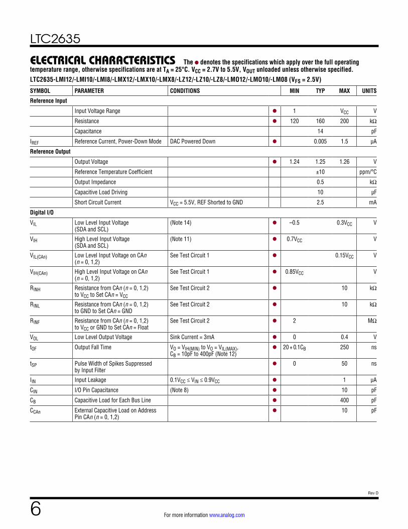
ELECTRICAL CHARACTERISTICS The l denotes the specifications which apply over the full operating temperature range, otherwise specifications are at TA = 25°C. VCC = 2.7V to 5.5V, VOUT unloaded unless otherwise specified.LTC2635-LMI12/-LMI10/-LMI8/-LMX12/-LMX10/-LMX8/-LZ12/-LZ10/-LZ8/-LMO12/-LMO10/-LM08 (VFS = 2.5V)
SYMBOL PARAMETER CONDITIONS MIN TYP MAX UNITS
Reference Input
Input Voltage Range l 1 VCC V
Resistance l 120 160 200 kΩ
Capacitance 14 pF
IREF Reference Current, Power-Down Mode DAC Powered Down l 0.005 1.5 µA
Reference Output
Output Voltage l 1.24 1.25 1.26 V
Reference Temperature Coefficient ±10 ppm/°C
Output Impedance 0.5 kΩ
Capacitive Load Driving 10 µF
Short Circuit Current VCC = 5.5V, REF Shorted to GND 2.5 mA
Digital I/O
VIL Low Level Input Voltage (SDA and SCL)
(Note 14) l –0.5 0.3VCC V
VIH High Level Input Voltage (SDA and SCL)
(Note 11) l 0.7VCC V
VIL(CAn) Low Level Input Voltage on CAn (n = 0, 1,2)
See Test Circuit 1 l 0.15VCC V
VIH(CAn) High Level Input Voltage on CAn (n = 0, 1,2)
See Test Circuit 1 l 0.85VCC V
RINH Resistance from CAn (n = 0, 1,2) to VCC to Set CAn = VCC
See Test Circuit 2 l 10 kΩ
RINL Resistance from CAn (n = 0, 1,2) to GND to Set CAn = GND
See Test Circuit 2 l 10 kΩ
RINF Resistance from CAn (n = 0, 1,2) to VCC or GND to Set CAn = Float
See Test Circuit 2 l 2 MΩ
VOL Low Level Output Voltage Sink Current = 3mA l 0 0.4 V
tOF Output Fall Time VO = VIH(MIN) to VO = VIL(MAX), CB = 10pF to 400pF (Note 12)
l 20 + 0.1CB 250 ns
tSP Pulse Width of Spikes Suppressed by Input Filter
l 0 50 ns
IIN Input Leakage 0.1VCC ≤ VIN ≤ 0.9VCC l 1 µA
CIN I/O Pin Capacitance (Note 8) l 10 pF
CB Capacitive Load for Each Bus Line l 400 pF
CCAn External Capacitive Load on Address Pin CAn (n = 0, 1,2)
l 10 pF
LTC2635
7Rev D
For more information www.analog.com
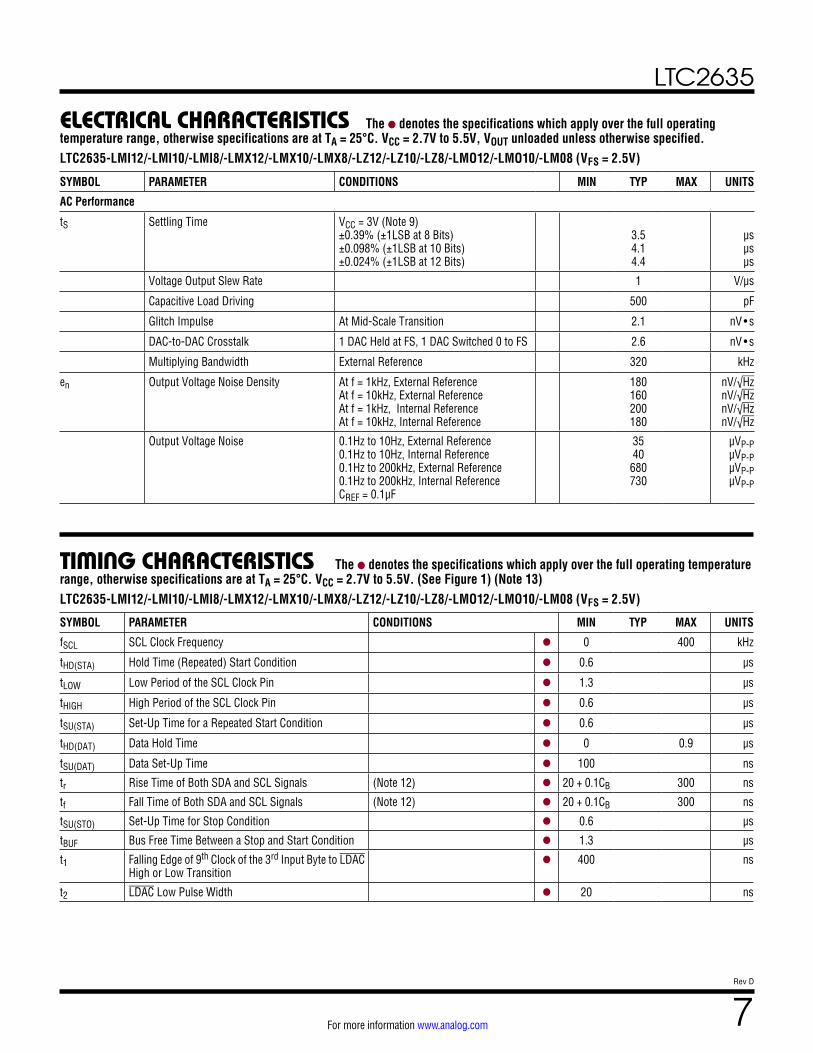
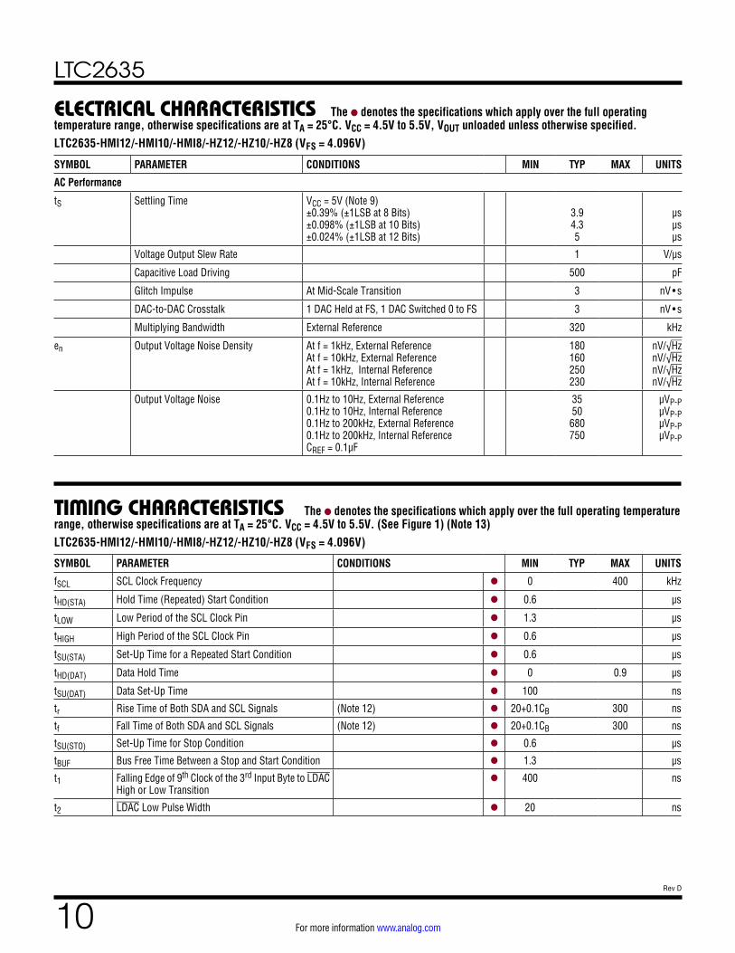
ELECTRICAL CHARACTERISTICS The l denotes the specifications which apply over the full operating temperature range, otherwise specifications are at TA = 25°C. VCC = 2.7V to 5.5V, VOUT unloaded unless otherwise specified.LTC2635-LMI12/-LMI10/-LMI8/-LMX12/-LMX10/-LMX8/-LZ12/-LZ10/-LZ8/-LMO12/-LMO10/-LM08 (VFS = 2.5V)
SYMBOL PARAMETER CONDITIONS MIN TYP MAX UNITS
AC Performance
tS Settling Time VCC = 3V (Note 9) ±0.39% (±1LSB at 8 Bits) ±0.098% (±1LSB at 10 Bits) ±0.024% (±1LSB at 12 Bits)
3.5 4.1 4.4
µs µs µs
Voltage Output Slew Rate 1 V/µs
Capacitive Load Driving 500 pF
Glitch Impulse At Mid-Scale Transition 2.1 nV • s
DAC-to-DAC Crosstalk 1 DAC Held at FS, 1 DAC Switched 0 to FS 2.6 nV • s
Multiplying Bandwidth External Reference 320 kHz
en Output Voltage Noise Density
At f = 1kHz, External Reference At f = 10kHz, External Reference At f = 1kHz, Internal Reference At f = 10kHz, Internal Reference
180 160 200 180
nV/√Hz nV/√Hz nV/√Hz nV/√Hz
Output Voltage Noise
0.1Hz to 10Hz, External Reference 0.1Hz to 10Hz, Internal Reference 0.1Hz to 200kHz, External Reference 0.1Hz to 200kHz, Internal Reference CREF = 0.1µF
35 40 680 730
µVP-P µVP-P µVP-P µVP-P
TIMING CHARACTERISTICS The l denotes the specifications which apply over the full operating temperature range, otherwise specifications are at TA = 25°C. VCC = 2.7V to 5.5V. (See Figure 1) (Note 13)LTC2635-LMI12/-LMI10/-LMI8/-LMX12/-LMX10/-LMX8/-LZ12/-LZ10/-LZ8/-LMO12/-LMO10/-LM08 (VFS = 2.5V)
SYMBOL PARAMETER CONDITIONS MIN TYP MAX UNITS
fSCL SCL Clock Frequency l 0 400 kHz
tHD(STA) Hold Time (Repeated) Start Condition l 0.6 µs
tLOW Low Period of the SCL Clock Pin l 1.3 µs
tHIGH High Period of the SCL Clock Pin l 0.6 µs
tSU(STA) Set-Up Time for a Repeated Start Condition l 0.6 µs
tHD(DAT) Data Hold Time l 0 0.9 µs
tSU(DAT) Data Set-Up Time l 100 ns
tr Rise Time of Both SDA and SCL Signals (Note 12) l 20 + 0.1CB 300 ns
tf Fall Time of Both SDA and SCL Signals (Note 12) l 20 + 0.1CB 300 ns
tSU(STO) Set-Up Time for Stop Condition l 0.6 µs
tBUF Bus Free Time Between a Stop and Start Condition l 1.3 µs
t1 Falling Edge of 9th Clock of the 3rd Input Byte to LDAC High or Low Transition
l 400 ns
t2 LDAC Low Pulse Width l 20 ns
LTC2635
8Rev D
For more information www.analog.com
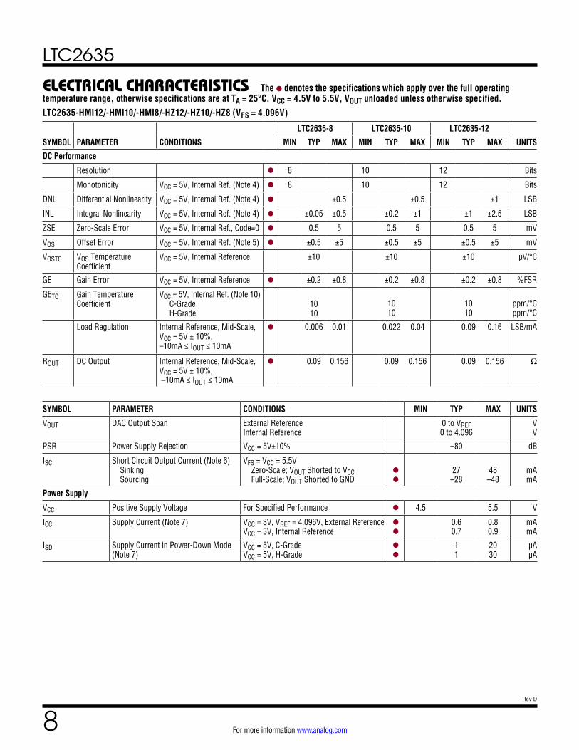
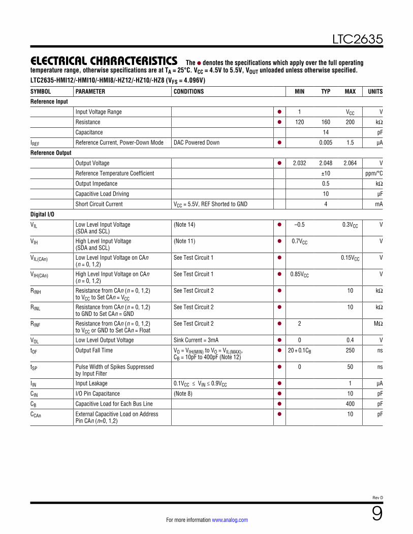
ELECTRICAL CHARACTERISTICS The l denotes the specifications which apply over the full operating temperature range, otherwise specifications are at TA = 25°C. VCC = 4.5V to 5.5V, VOUT unloaded unless otherwise specified.LTC2635-HMI12/-HMI10/-HMI8/-HZ12/-HZ10/-HZ8 (VFS = 4.096V)
SYMBOL PARAMETER CONDITIONS
LTC2635-8 LTC2635-10 LTC2635-12
UNITSMIN TYP MAX MIN TYP MAX MIN TYP MAX
DC Performance
Resolution l 8 10 12 Bits
Monotonicity VCC = 5V, Internal Ref. (Note 4) l 8 10 12 Bits
DNL Differential Nonlinearity VCC = 5V, Internal Ref. (Note 4) l ±0.5 ±0.5 ±1 LSB
INL Integral Nonlinearity VCC = 5V, Internal Ref. (Note 4) l ±0.05 ±0.5 ±0.2 ±1 ±1 ±2.5 LSB
ZSE Zero-Scale Error VCC = 5V, Internal Ref., Code=0 l 0.5 5 0.5 5 0.5 5 mV
VOS Offset Error VCC = 5V, Internal Ref. (Note 5) l ±0.5 ±5 ±0.5 ±5 ±0.5 ±5 mV
VOSTC VOS Temperature Coefficient
VCC = 5V, Internal Reference ±10 ±10 ±10 µV/°C
GE Gain Error VCC = 5V, Internal Reference l ±0.2 ±0.8 ±0.2 ±0.8 ±0.2 ±0.8 %FSR
GETC Gain Temperature Coefficient
VCC = 5V, Internal Ref. (Note 10) C-Grade H-Grade
10 10
10 10
10 10
ppm/°C ppm/°C
Load Regulation Internal Reference, Mid-Scale, VCC = 5V ± 10%, –10mA ≤ IOUT ≤ 10mA
l 0.006 0.01 0.022 0.04 0.09 0.16 LSB/mA
ROUT DC Output Internal Reference, Mid-Scale, VCC = 5V ± 10%, –10mA ≤ IOUT ≤ 10mA
l 0.09 0.156 0.09 0.156 0.09 0.156 Ω
SYMBOL PARAMETER CONDITIONS MIN TYP MAX UNITS
VOUT DAC Output Span External Reference Internal Reference
0 to VREF 0 to 4.096
V V
PSR Power Supply Rejection VCC = 5V±10% –80 dB
ISC Short Circuit Output Current (Note 6) Sinking Sourcing
VFS = VCC = 5.5V Zero-Scale; VOUT Shorted to VCC Full-Scale; VOUT Shorted to GND
l
l
27
–28
48 –48
mA mA
Power Supply
VCC Positive Supply Voltage For Specified Performance l 4.5 5.5 V
ICC Supply Current (Note 7) VCC = 3V, VREF = 4.096V, External Reference VCC = 3V, Internal Reference
l
l
0.6 0.7
0.8 0.9
mA mA
ISD Supply Current in Power-Down Mode (Note 7)
VCC = 5V, C-Grade VCC = 5V, H-Grade
l
l
1 1
20 30
µA µA
LTC2635
9Rev D
For more information www.analog.com
SYMBOL PARAMETER CONDITIONS MIN TYP MAX UNITS
Reference Input
Input Voltage Range l 1 VCC V
Resistance l 120 160 200 kΩ
Capacitance 14 pF
IREF Reference Current, Power-Down Mode DAC Powered Down l 0.005 1.5 µA
Reference Output
Output Voltage l 2.032 2.048 2.064 V
Reference Temperature Coefficient ±10 ppm/°C
Output Impedance 0.5 kΩ
Capacitive Load Driving 10 µF
Short Circuit Current VCC = 5.5V, REF Shorted to GND 4 mA
Digital I/O
VIL Low Level Input Voltage (SDA and SCL)
(Note 14) l –0.5 0.3VCC V
VIH High Level Input Voltage (SDA and SCL)
(Note 11) l 0.7VCC V
VIL(CAn) Low Level Input Voltage on CAn (n = 0, 1,2)
See Test Circuit 1 l 0.15VCC V
VIH(CAn) High Level Input Voltage on CAn (n = 0, 1,2)
See Test Circuit 1 l 0.85VCC V
RINH Resistance from CAn (n = 0, 1,2) to VCC to Set CAn = VCC
See Test Circuit 2 l 10 kΩ
RINL Resistance from CAn (n = 0, 1,2) to GND to Set CAn = GND
See Test Circuit 2 l 10 kΩ
RINF Resistance from CAn (n = 0, 1,2) to VCC or GND to Set CAn = Float
See Test Circuit 2 l 2 MΩ
VOL Low Level Output Voltage Sink Current = 3mA l 0 0.4 V
tOF Output Fall Time VO = VIH(MIN) to VO = VIL(MAX), CB = 10pF to 400pF (Note 12)
l 20 + 0.1CB 250 ns
tSP Pulse Width of Spikes Suppressed by Input Filter
l 0 50 ns
IIN Input Leakage 0.1VCC ≤ VIN ≤ 0.9VCC l 1 µA
CIN I/O Pin Capacitance (Note 8) l 10 pF
CB Capacitive Load for Each Bus Line l 400 pF
CCAn External Capacitive Load on Address Pin CAn (n=0, 1,2)
l 10 pF
ELECTRICAL CHARACTERISTICS The l denotes the specifications which apply over the full operating temperature range, otherwise specifications are at TA = 25°C. VCC = 4.5V to 5.5V, VOUT unloaded unless otherwise specified.LTC2635-HMI12/-HMI10/-HMI8/-HZ12/-HZ10/-HZ8 (VFS = 4.096V)
LTC2635
10Rev D
For more information www.analog.com
ELECTRICAL CHARACTERISTICS The l denotes the specifications which apply over the full operating temperature range, otherwise specifications are at TA = 25°C. VCC = 4.5V to 5.5V, VOUT unloaded unless otherwise specified.LTC2635-HMI12/-HMI10/-HMI8/-HZ12/-HZ10/-HZ8 (VFS = 4.096V)
SYMBOL PARAMETER CONDITIONS MIN TYP MAX UNITS
AC Performance
tS Settling Time VCC = 5V (Note 9) ±0.39% (±1LSB at 8 Bits) ±0.098% (±1LSB at 10 Bits) ±0.024% (±1LSB at 12 Bits)
3.9 4.3 5
µs µs µs
Voltage Output Slew Rate 1 V/µs
Capacitive Load Driving 500 pF
Glitch Impulse At Mid-Scale Transition 3 nV • s
DAC-to-DAC Crosstalk 1 DAC Held at FS, 1 DAC Switched 0 to FS 3 nV • s
Multiplying Bandwidth External Reference 320 kHz
en Output Voltage Noise Density
At f = 1kHz, External Reference At f = 10kHz, External Reference At f = 1kHz, Internal Reference At f = 10kHz, Internal Reference
180 160 250 230
nV/√Hz nV/√Hz nV/√Hz nV/√Hz
Output Voltage Noise
0.1Hz to 10Hz, External Reference 0.1Hz to 10Hz, Internal Reference 0.1Hz to 200kHz, External Reference 0.1Hz to 200kHz, Internal Reference CREF = 0.1µF
35 50 680 750
µVP-P µVP-P µVP-P µVP-P
TIMING CHARACTERISTICS The l denotes the specifications which apply over the full operating temperature range, otherwise specifications are at TA = 25°C. VCC = 4.5V to 5.5V. (See Figure 1) (Note 13)LTC2635-HMI12/-HMI10/-HMI8/-HZ12/-HZ10/-HZ8 (VFS = 4.096V)
SYMBOL PARAMETER CONDITIONS MIN TYP MAX UNITS
fSCL SCL Clock Frequency l 0 400 kHz
tHD(STA) Hold Time (Repeated) Start Condition l 0.6 µs
tLOW Low Period of the SCL Clock Pin l 1.3 µs
tHIGH High Period of the SCL Clock Pin l 0.6 µs
tSU(STA) Set-Up Time for a Repeated Start Condition l 0.6 µs
tHD(DAT) Data Hold Time l 0 0.9 µs
tSU(DAT) Data Set-Up Time l 100 ns
tr Rise Time of Both SDA and SCL Signals (Note 12) l 20+0.1CB 300 ns
tf Fall Time of Both SDA and SCL Signals (Note 12) l 20+0.1CB 300 ns
tSU(STO) Set-Up Time for Stop Condition l 0.6 µs
tBUF Bus Free Time Between a Stop and Start Condition l 1.3 µs
t1 Falling Edge of 9th Clock of the 3rd Input Byte to LDAC High or Low Transition
l 400 ns
t2 LDAC Low Pulse Width l 20 ns
LTC2635
11Rev D
For more information www.analog.com
Note 1: Stresses beyond those listed under Absolute Maximum Ratings may cause permanent damage to the device. Exposure to any Absolute Maximum Rating condition for extended periods may affect device reliability and lifetime.
Note 2: All voltages are with respect to GND.
Note 3: Operating at temperatures above 90°C and with VCC > 4V requires VCC slew rates to be no greater than 73mV/us.
Note 4: Linearity and monotonicity are defined from code kL to code 2N – 1, where N is the resolution and kL is given by kL = 0.016 • (2N/ VFS), rounded to the nearest whole code. For VFS = 2.5V and N = 12, kL = 26 and linearity is defined from code 26 to code 4,095. For VFS = 4.096V and N = 12, kL = 16 and linearity is defined from code 16 to code 4,095.
Note 5: Inferred from measurement at code 16 (LTC2635-12), code 4 (LTC2635-10) or code 1 (LTC2635-8), and at full-scale.
Note 6: This IC includes current limiting that is intended to protect the device during momentary overload conditions. Junction temperature can exceed the rated maximum during current limiting. Continuous operation above
the specified maximum operating junction temperature may impair device reliability.
Note 7: Digital inputs at 0V or VCC.
Note 8: Guaranteed by design and not production tested.
Note 9: Internal Reference mode. DAC is stepped 1/4 scale to 3/4 scale and 3/4 scale to 1/4 scale. Load is 2kΩ in parallel with 100pF to GND.
Note 10: Temperature coefficient is calculated by dividing the maximum change in output voltage by the specified temperature range.
Note 11: Maximum VIH = VCC(MAX) + 0.5V.
Note 12: CB = capacitance of one bus line in pF.
Note 13: All values refer to VIH = VIH(MIN) and VIL = VIL(MAX) levels.
Note 14: Minimum VIL exceeds the Absolute Maximum rating. This condition won’t damage the IC, but could degrade performance.
ELECTRICAL CHARACTERISTICS
LTC2635
12Rev D
For more information www.analog.com
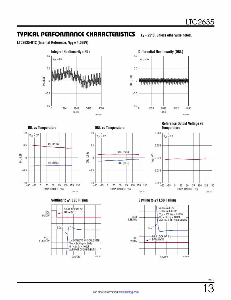
TYPICAL PERFORMANCE CHARACTERISTICS
Integral Nonlinearity (INL) Differential Nonlinearity (DNL)
INL vs Temperature DNL vs TemperatureReference Output Voltage vs Temperature
Settling to ±1 LSB Rising Settling to ±1 LSB Falling
TA = 25°C, unless otherwise noted.
CODE0
INL
(LSB
)
1.0
0.5
0
–0.5
–1.01024 3072
2635 G01
40952048
VCC = 3V
CODE0
DNL
(LSB
)
1.0
0.5
0
–0.5
–1.01024 3072
2635 G02
40952048
VCC = 3V
TEMPERATURE (°C)–50
INL
(LSB
)
1.0
0.5
0
–0.5
–1.0–25 125100755025
2635 G03
1500
VCC = 3V
INL (POS)
INL (NEG)
TEMPERATURE (°C)–50
DNL
(LSB
)
1.0
0.5
0
–0.5
–1.0–25 125100755025
2635 G04
1500
VCC = 3V
DNL (POS)
DNL (NEG)
TEMPERATURE (°C)–50
V REF
(V)
1.260
1.255
1.250
1.245
1.240–25 125100755025
2635 G05
1500
VCC = 3V
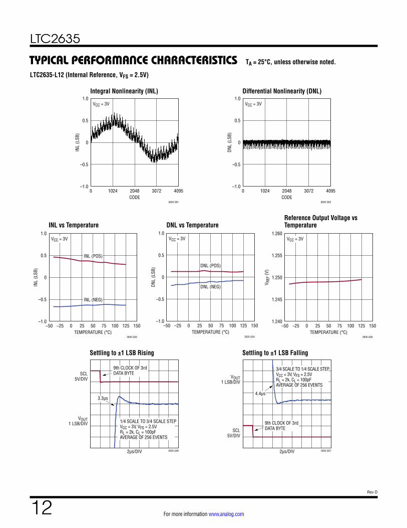
LTC2635-L12 (Internal Reference, VFS = 2.5V)
2µs/DIV
VOUT1 LSB/DIV
SCL5V/DIV
2635 G06
3.3µs
9th CLOCK OF 3rdDATA BYTE
1/4 SCALE TO 3/4 SCALE STEPVCC = 3V, VFS = 2.5VRL = 2k, CL = 100pFAVERAGE OF 256 EVENTS
2µs/DIV
VOUT1 LSB/DIV
SCL5V/DIV
2635 G07
3/4 SCALE TO 1/4 SCALE STEPVCC = 3V, VFS = 2.5VRL = 2k, CL = 100pFAVERAGE OF 256 EVENTS
4.4µs
9th CLOCK OF 3rdDATA BYTE
LTC2635
13Rev D
For more information www.analog.com
TYPICAL PERFORMANCE CHARACTERISTICS
Integral Nonlinearity (INL) Differential Nonlinearity (DNL)
INL vs Temperature DNL vs TemperatureReference Output Voltage vs Temperature
Settling to ±1 LSB Rising Settling to ±1 LSB Falling
LTC2635-H12 (Internal Reference, VFS = 4.096V)
CODE0
INL
(LSB
)
1.0
0.5
0
–0.5
–1.01024 3072
2635 G08
40952048
VCC = 5V
CODE0
DNL
(LSB
)
1.0
0.5
0
–0.5
–1.01024 3072
2635 G09
40952048
VCC = 5V
TEMPERATURE (°C)–50
INL
(LSB
)
1.0
0.5
0
–0.5
–1.0–25 125100755025
2635 G10
1500
VCC = 5V
INL (POS)
INL (NEG)
TEMPERATURE (°C)–50
DNL
(LSB
)
1.0
0.5
0
–0.5
–1.0–25 125100755025
2635 G11
1500
VCC = 5V
DNL (POS)
DNL (NEG)
TEMPERATURE (°C)–50
V REF
(V)
2.068
2.058
2.048
2.038
2.028–25 125100755025
2635 G12
1500
VCC = 5V
TA = 25°C, unless otherwise noted.
2µs/DIV
VOUT1 LSB/DIV
SCL5V/DIV
2635 G13
1/4 SCALE TO 3/4 SCALE STEPVCC = 5V, VFS = 4.095VRL = 2k, CL = 100pFAVERAGE OF 256 EVENTS
3.9µs
9th CLOCK OF 3rdDATA BYTE
2µs/DIV
VOUT1 LSB/DIV
SCL5V/DIV
2635 G14
3/4 SCALE TO 1/4 SCALE STEPVCC = 5V, VFS = 4.095VRL = 2k, CL = 100pFAVERAGE OF 256 EVENTS
5µs
9th CLOCK OF 3rdDATA BYTE
LTC2635
14Rev D
For more information www.analog.com
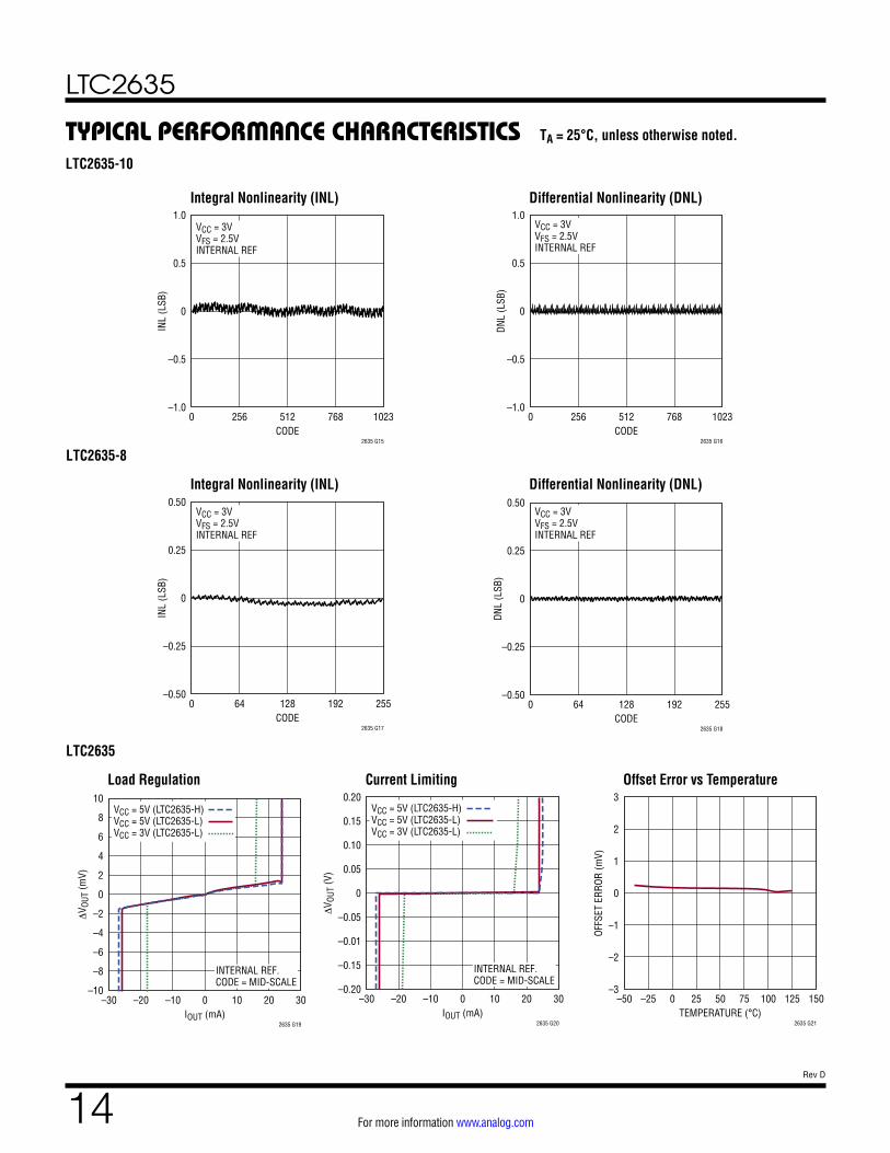
TYPICAL PERFORMANCE CHARACTERISTICS
Integral Nonlinearity (INL) Differential Nonlinearity (DNL)
LTC2635-10
Integral Nonlinearity (INL) Differential Nonlinearity (DNL)
LTC2635-8
Load Regulation Current Limiting
LTC2635
Offset Error vs Temperature
TA = 25°C, unless otherwise noted.
CODE0
INL
(LSB
)
1.0
0.5
0
–0.5
–1.0256 768
2635 G15
1023512
VCC = 3VVFS = 2.5VINTERNAL REF
CODE0
DNL
(LSB
)
1.0
0.5
0
–0.5
–1.0256 768
2635 G16
1023512
VCC = 3VVFS = 2.5VINTERNAL REF
CODE0
INL
(LSB
)
0.50
0.25
0
–0.25
–0.5064 192
2635 G17
255128
VCC = 3VVFS = 2.5VINTERNAL REF
CODE0
DNL
(LSB
)0.50
0.25
0
–0.25
–0.5064 192
2635 G18
255128
VCC = 3VVFS = 2.5VINTERNAL REF
IOUT (mA)–30
ΔV O
UT (m
V)
10
8
6
4
2
–6
–4
–2
0
–8
–10–20 20100
2635 G19
30–10
VCC = 5V (LTC2635-H)VCC = 5V (LTC2635-L)VCC = 3V (LTC2635-L)
INTERNAL REF.CODE = MID-SCALE
IOUT (mA)–30
ΔV O
UT (V
)
0.20
0.15
0.10
0.05
–0.15
–0.01
–0.05
0
–0.20–20 20100
2635 G20
30–10
VCC = 5V (LTC2635-H)VCC = 5V (LTC2635-L)VCC = 3V (LTC2635-L)
INTERNAL REF.CODE = MID-SCALE
TEMPERATURE (°C)–50
OFFS
ET E
RROR
(mV)
3
2
1
0
–1
–2
–3–25 125100755025
2635 G21
1500
LTC2635
15Rev D
For more information www.analog.com
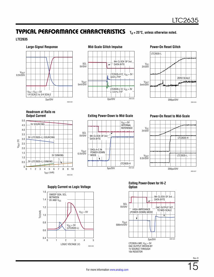
TYPICAL PERFORMANCE CHARACTERISTICS
Large-Signal Response Mid-Scale Glitch Impulse Power-On Reset Glitch
Headroom at Rails vs Output Current Exiting Power-Down to Mid-Scale Power-On Reset to Mid-Scale
Supply Current vs Logic Voltage
LTC2635
TA = 25°C, unless otherwise noted.
2µs/DIV
VOUT0.5V/DIV
2635 G22
VFS = VCC = 5V1/4 SCALE to 3/4 SCALE
200µs/DIV
VOUT5mV/DIV
VCC2V/DIV
2635 G24
LTC2635-L
ZERO SCALE
IOUT (mA)0
V OUT
(V)
5.0
4.5
1.0
1.5
2.0
2.5
3.0
3.5
4.0
0.5
01 7 8 96543
2635 G25
102
5V SOURCING
3V (LTC2635-L) SOURCING
3V (LTC2635-L) SINKING
5V SINKING
200µs/DIV
VCC2V/DIV
VOUT0.5V/DIV
2635 G27
LTC2635-H
LTC2635-L
Exiting Power-Down for Hi-Z Option
5µs/DIV
VOUT0.5V/DIV
SCL5V/DIV
2635 G26
9th CLOCK OF 3rdDATA BYTE
LTC2635-H
DACs A-C INPOWER-DOWN MODE
VCC = 5VINTERNALREFERENCE
LOGIC VOLTAGE (V)
00.4
0.6
0.8
1.0
1.2
1.4
1.6
1 2 3 4 5
I CC(
mA)
2635 G28
SWEEP SDA, SCLBETWEEN0V AND VCC
VCC = 5V
VCC = 3V(LTC2635-L)
2µs/DIV
LTC2635-LMO, VCC = 3V DAC OUTPUT DRIVEN BY1V SOURCE THROUGH15k RESISTOR
VOUT500mV/DIV
SCL5V/DIV
2635 G29
HIGH-IMPEDANCE(POWER-DOWN) MODE
DAC OUTPUT SETTO MID-SCALE
9th CLOCK OF 3rdDATA BYTE
2µs/DIV
VOUT5mV/DIV
SCL5V/DIV
2635 G23
9th CLOCK OF 3rdDATA BYTE
LTC2635-H12, VCC = 5V3nV • s TYP
LTC2635-L12, VCC = 3V2.1nV • s TYP
LTC2635
16Rev D
For more information www.analog.com
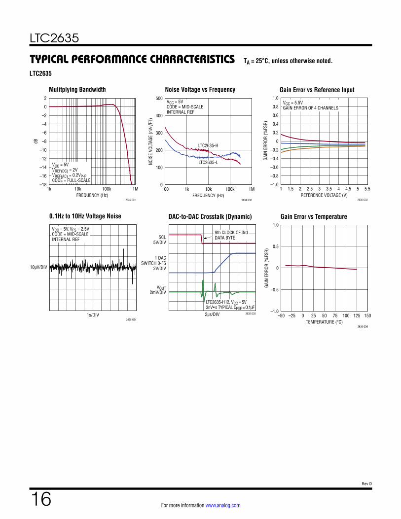
TYPICAL PERFORMANCE CHARACTERISTICS
Mulitplying Bandwidth Noise Voltage vs Frequency Gain Error vs Reference Input
0.1Hz to 10Hz Voltage Noise DAC-to-DAC Crosstalk (Dynamic) Gain Error vs Temperature
LTC2635
TA = 25°C, unless otherwise noted.
FREQUENCY (Hz)
dB
2635 G31
2
0
–16
–14
–12
–10
–8
–6
–4
–2
–181k 100k 1M10k
VCC = 5VVREF(DC) = 2VVREF(AC) = 0.2VP-PCODE = FULL-SCALE
FREQUENCY (Hz)100
NOIS
E VO
LTAG
E (n
V/√H
z)
500
400
300
200
100
01k 100k
2634 G32
1M10k
VCC = 5VCODE = MID-SCALEINTERNAL REF
LTC2635-H
LTC2635-L
REFERENCE VOLTAGE (V)1
GAI
N ER
ROR
(%FS
R)
1.0
0.8
0.6
0.4
–0.6
–0.8
–0.4
–0.2
0.2
0
–1.01.5 54.54
2635 G33
5.52 2.5 3 3.5
VCC = 5.5VGAIN ERROR OF 4 CHANNELS
1s/DIV
10µV/DIV
2635 G34
VCC = 5V, VFS = 2.5VCODE = MID-SCALEINTERNAL REF
TEMPERATURE (°C)–50
GAIN
ERR
OR (%
FSR)
1.0
0.5
0
–0.5
–1.0–25 125100755025
2635 G36
15002µs/DIV
1 DACSWITCH 0-FS
2V/DIV
VOUT2mV/DIV
SCL5V/DIV
2635 G35
9th CLOCK OF 3rdDATA BYTE
LTC2635-H12, VCC = 5V3nV • s TYPICAL CREF = 0.1µF
LTC2635
17Rev D
For more information www.analog.com
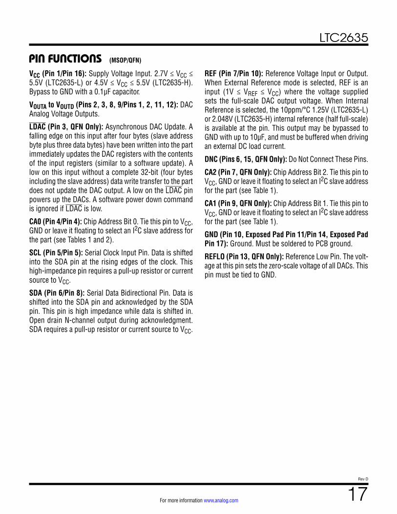
PIN FUNCTIONSVCC (Pin 1/Pin 16): Supply Voltage Input. 2.7V ≤ VCC ≤ 5.5V (LTC2635-L) or 4.5V ≤ VCC ≤ 5.5V (LTC2635-H). Bypass to GND with a 0.1µF capacitor.
VOUTA to VOUTD (Pins 2, 3, 8, 9/Pins 1, 2, 11, 12): DAC Analog Voltage Outputs.
LDAC (Pin 3, QFN Only): Asynchronous DAC Update. A falling edge on this input after four bytes (slave address byte plus three data bytes) have been written into the part immediately updates the DAC registers with the contents of the input registers (similar to a software update). A low on this input without a complete 32-bit (four bytes including the slave address) data write transfer to the part does not update the DAC output. A low on the LDAC pin powers up the DACs. A software power down command is ignored if LDAC is low.
CA0 (Pin 4/Pin 4): Chip Address Bit 0. Tie this pin to VCC, GND or leave it floating to select an I2C slave address for the part (see Tables 1 and 2).
SCL (Pin 5/Pin 5): Serial Clock Input Pin. Data is shifted into the SDA pin at the rising edges of the clock. This high-impedance pin requires a pull-up resistor or current source to VCC.
SDA (Pin 6/Pin 8): Serial Data Bidirectional Pin. Data is shifted into the SDA pin and acknowledged by the SDA pin. This pin is high impedance while data is shifted in. Open drain N-channel output during acknowledgment. SDA requires a pull-up resistor or current source to VCC.
REF (Pin 7/Pin 10): Reference Voltage Input or Output. When External Reference mode is selected, REF is an input (1V ≤ VREF ≤ VCC) where the voltage supplied sets the full-scale DAC output voltage. When Internal Reference is selected, the 10ppm/°C 1.25V (LTC2635-L) or 2.048V (LTC2635-H) internal reference (half full-scale) is available at the pin. This output may be bypassed to GND with up to 10µF, and must be buffered when driving an external DC load current.
DNC (Pins 6, 15, QFN Only): Do Not Connect These Pins.
CA2 (Pin 7, QFN Only): Chip Address Bit 2. Tie this pin to VCC, GND or leave it floating to select an I2C slave address for the part (see Table 1).
CA1 (Pin 9, QFN Only): Chip Address Bit 1. Tie this pin to VCC, GND or leave it floating to select an I2C slave address for the part (see Table 1).
GND (Pin 10, Exposed Pad Pin 11/Pin 14, Exposed Pad Pin 17): Ground. Must be soldered to PCB ground.
REFLO (Pin 13, QFN Only): Reference Low Pin. The volt-age at this pin sets the zero-scale voltage of all DACs. This pin must be tied to GND.
(MSOP/QFN)
LTC2635
18Rev D
For more information www.analog.com
BLOCK DIAGRAM
REGI
STER
REGI
STER
REGI
STER
REGI
STER
DAC AVOUTA
(REFLO)
(LDAC)
CA0
(CA1)
(CA2)
( ) QFN PACKAGE ONLY
GND
VOUTB
VREF
DAC D
REGI
STER
REGI
STER
REGI
STER
REGI
STER
DAC B DAC C
VREF
VOUTD
REF
VCC
VREF
VOUTC
SWITCHINTERNALREFERENCE
I2C INTERFACE
DECODE
I2CADDRESSDECODE
POWER-ONRESET
SCL
SDA
2635 BD
LTC2635
19Rev D
For more information www.analog.com
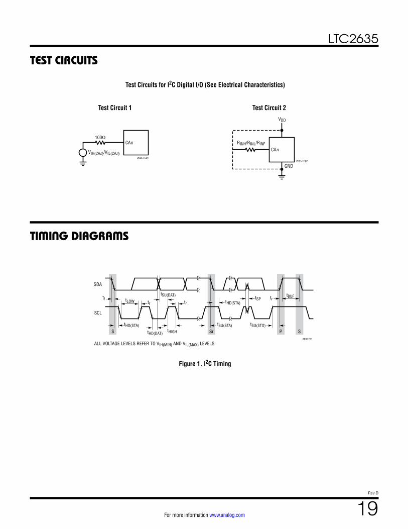
TEST CIRCUITS
TIMING DIAGRAMS
2635 TC01
100Ω
VIH(CAn)/VIL(CAn)
CAn
2635 TC02
RINH/RINL/RINF
VDD
GND
CAn
ALL VOLTAGE LEVELS REFER TO VIH(MIN) AND VIL(MAX) LEVELS
SDA
tLOW
tHD(STA) tSU(STA)
2635 F01
tSU(STO)
tHD(DAT)
tSU(DAT)
tHIGH
tftr tr tHD(STA)
tSPtBUFtr
SCL
S Sr P S
Test Circuit 1 Test Circuit 2
Figure 1. I2C Timing
Test Circuits for I2C Digital I/O (See Electrical Characteristics)
LTC2635
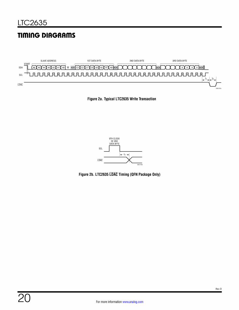
20Rev D
For more information www.analog.com
9TH CLOCKOF 3RD
DATA BYTE
2635 F02b
t1
SCL
LDAC
Figure 2a. Typical LTC2635 Write Transaction
Figure 2b. LTC2635 LDAC Timing (QFN Package Only)
TIMING DIAGRAMS
C3 C2 C1 C0 A3 A2 A1 A0 ACKACKACKACKA0 WA1A2A3A4A5
1 2 3 4 5 6 7 8 9 1 2 3 4 5 6 7 8 9 1 2 3 4 5 6 7 8 9 1 2 3 4 5 6 7 8 9
A6
STARTSLAVE ADDRESS 1ST DATA BYTE 2ND DATA BYTE 3RD DATA BYTE
SDA
SCL
LDAC2635 F02a
X X X X
t1 t2
LTC2635
21Rev D
For more information www.analog.com
OPERATIONThe LTC2635 is a family of quad voltage output DACs in 16-pin QFN and 10-lead MSOP packages. Each DAC can operate rail-to-rail using an external reference, or with its full-scale voltage set by an integrated reference. Eighteen combinations of accuracy (12-, 10-, and 8-bit), power-on reset value (zero-scale, mid-scale in internal reference mode, or mid-scale in external reference mode), DAC power-down output load (high impedance or 200kΩ), and full-scale voltage (2.5V or 4.096V) are available. The LTC2635 is controlled using a 2-wire I2C interface.
Power-On Reset
The LTC2635-HZ/-LZ clear the output to zero-scale when power is first applied, making system initialization con-sistent and repeatable.
For some applications, downstream circuits are active during DAC power-up, and may be sensitive to nonzero outputs from the DAC during this time. The LTC2635 contains circuitry to reduce the power-on glitch: the analog output typically rises less than 5mV above zero-scale during power on. In general, the glitch amplitude decreases as the power supply ramp time is increased. See “Power-On Reset Glitch” in the Typical Performance Characteristics section.
The LTC2635-HMI/-LMI/-LMX provide an alternative reset, setting the output to mid-scale when power is first applied. The LTC2635-LMI and LTC2635-HMI power up in internal reference mode, with the output set to a mid-scale voltage of 1.25V and 2.048V, respectively. The LTC2635-LMX power-up in external reference mode, with the output set to mid-scale of the external reference. The LTC2635-LMO powers up in internal reference mode with all the DAC channels placed in the high-impedance state (powered-down). Input and DAC registers are set to the mid-scale code, and only the internal reference is powered up, causing supply current to be typically 100µA upon power up. Default reference mode selection is described in the Reference Modes section.
Power Supply Sequencing
The voltage at REF (Pin 10 – QFN, Pin 7 – MSOP) must be kept within the range –0.3V ≤ VREF ≤ VCC + 0.3V (see Absolute Maximum Ratings). Particular care should be
taken to observe these limits during power supply turn-on and turn-off sequences, when the voltage at VCC is in transition.
Transfer Function
The digital-to-analog transfer function is
VOUT(IDEAL) =
k
2N
⎛
⎝⎜
⎞
⎠⎟ VREF – VREFLO( ) + VREFLO
where k is the decimal equivalent of the binary DAC input code, N is the resolution, and VREF is either 2.5V (LTC2635-LMI/-LMX/-LMO/-LZ) or 4.096V (LTC2635-HMI/-HZ) when in Internal Reference mode, and the volt-age at REF when in External Reference mode.
I2C Serial Interface
The LTC2635 communicates with a host using the stan-dard 2-wire I2C interface. The timing diagrams (Figures 1 and 2) show the timing relationship of the signals on the bus. The two bus lines, SDA and SCL, must be high when the bus is not in use. External pull-up resistors or current sources are required on these lines. The value of these pull-up resistors is dependent on the power supply and can be obtained from the I2C specifications. For an I2C bus operating in the fast mode, an active pull-up will be necessary if the bus capacitance is greater than 200pF.
The LTC2635 is a receive-only (slave) device. The master can write to the LTC2635. The LTC2635 will not acknowl-edge (NAK) a read request from the master.
START (S) and STOP (P) Conditions
When the bus is not in use, both SCL and SDA must be high. A bus master signals the beginning of a communica-tion to a slave device by transmitting a START condition. A START condition is generated by transitioning SDA from high to low while SCL is high.
When the master has finished communicating with the slave, it issues a STOP condition. A STOP condition is generated by transitioning SDA from low to high while SCL is high. The bus is then free for communication with another I2C device.
LTC2635
22Rev D
For more information www.analog.com
Acknowledge
The Acknowledge (ACK) signal is used for handshaking between the master and the slave. An ACK (active LOW) generated by the slave lets the master know that the lat-est byte of information was properly received. The ACK related clock pulse is generated by the master. The mas-ter releases the SDA line (HIGH) during the ACK clock pulse. The slave-receiver must pull down the SDA bus line during the ACK clock pulse so that it remains a sta-ble LOW during the HIGH period of this clock pulse. The LTC2635 responds to a write by a master in this manner but does not acknowledge a read operation; in that case, SDA is retained HIGH during the period of the ACK clock pulse.
Chip Address
The state of pins CA0, CA1 and CA2 (CA1 and CA2 are only available on the QFN package) determines the slave address of the part. These pins can be each set to any one of three states: VCC, GND or float. This results in 27 (QFN Package) or 3 (MSOP Package) selectable addresses for the part. The slave address assignments are shown in Tables 1 and 2.
In addition to the address selected by the address pins, the part also responds to a global address. This address allows a common write to all LTC2635 parts to be ac-com-plished using one 3-byte write transaction on the I2C bus. The global address, listed at the end of Tables 1 and 2, is a 7-bit hardwired address not selectable by CA0, CA1 or CA2. If another address is required, please consult the factory.
The maximum capacitive load allowed on the address pins (CA0, CA1 and CA2) is 10pF, as these pins are driven during address detection to determine if they are floating.
Table 1. Slave Address Map (QFN Package)CA2 CA1 CA0 A6 A5 A4 A3 A2 A1 A0
GND GND GND 0 0 1 0 0 0 0
GND GND FLOAT 0 0 1 0 0 0 1
GND GND VCC 0 0 1 0 0 1 0
GND FLOAT GND 0 0 1 0 0 1 1
GND FLOAT FLOAT 0 1 0 0 0 0 0
GND FLOAT VCC 0 1 0 0 0 0 1
GND VCC GND 0 1 0 0 0 1 0
GND VCC FLOAT 0 1 0 0 0 1 1
GND VCC VCC 0 1 1 0 0 0 0
FLOAT GND GND 0 1 1 0 0 0 1
FLOAT GND FLOAT 0 1 1 0 0 1 0
FLOAT GND VCC 0 1 1 0 0 1 1
FLOAT FLOAT GND 1 0 0 0 0 0 0
FLOAT FLOAT FLOAT 1 0 0 0 0 0 1
FLOAT FLOAT VCC 1 0 0 0 0 1 0
FLOAT VCC GND 1 0 0 0 0 1 1
FLOAT VCC FLOAT 1 0 1 0 0 0 0
FLOAT VCC VCC 1 0 1 0 0 0 1
VCC GND GND 1 0 1 0 0 1 0
VCC GND FLOAT 1 0 1 0 0 1 1
VCC GND VCC 1 1 0 0 0 0 0
VCC FLOAT GND 1 1 0 0 0 0 1
VCC FLOAT FLOAT 1 1 0 0 0 1 0
VCC FLOAT VCC 1 1 0 0 0 1 1
VCC VCC GND 1 1 1 0 0 0 0
VCC VCC FLOAT 1 1 1 0 0 0 1
VCC VCC VCC 1 1 1 0 0 1 0
GLOBAL ADDRESS 1 1 1 0 0 1 1
Table 2. Slave Address Map (MSOP Package)CA0 A6 A5 A4 A3 A2 A1 A0
GND 0 0 1 0 0 0 0
FLOAT 0 0 1 0 0 0 1
VCC 0 0 1 0 0 1 0
GLOBAL ADDRESS 1 1 1 0 0 1 1
OPERATION
LTC2635
23Rev D
For more information www.analog.com
Write Word Protocol
The master initiates communication with the LTC2635 with a START condition and a 7-bit slave address followed by the Write bit (W) = 0. The LTC2635 acknowledges by pulling the SDA pin low at the 9th clock if the 7-bit slave address matches the address of the part (set by CA0, CA1 or CA2) or the global address. The master then transmits three bytes of data. The LTC2635 acknowledges each byte of data by pulling the SDA line low at the 9th clock of each data byte transmission. After receiving three complete bytes of data, the LTC2635 executes the command spec-ified in the 24-bit input word.
If more than three data bytes are transmitted after a valid 7-bit slave address, the LTC2635 does not acknowledge (NAK) the extra bytes of data (SDA is high during the 9th clock).
The format of the three data bytes is shown in Figure 3. The first byte of the input word consists of the 4-bit com-mand, followed by the 4-bit DAC address. The next two bytes contain the 16-bit data word, which consists of the 12-, 10- or 8-bit input code, MSB to LSB, followed by 4, 6 or 8 don’t-care bits (LTC2635-12, -10 and -8, respec-tively). A typical LTC2635 write transaction is shown in Figure 4.
The command bit assignments (C3-C0) and address (A3-A0) assignments are shown in Tables 3 and 4. The first four commands in the table consist of write and update operations. A write operation loads a 16-bit data word from the 32-bit shift register into the input register. In an update operation, the data word is copied from the input register to the DAC register. Once copied into the DAC register, the data word becomes the active 12-, 10-, or 8-bit input code, and is converted to an analog voltage at the DAC output. Write to and Update combines the first two commands. The Update operation also powers up the
DAC if it had been in power-down mode. The data path and registers are shown in the Block Diagram.
Table 3. Command CodesCOMMAND*
C3 C2 C1 C0
0 0 0 0 Write to Input Register n
0 0 0 1 Update (Power Up) DAC Register n
0 0 1 0 Write to Input Register n, Update (Power Up) All
0 0 1 1 Write to and Update (Power Up) DAC Register n
0 1 0 0 Power Down n
0 1 0 1 Power Down Chip (All DAC’s and Reference)
0 1 1 0 Select Internal Reference (Power Up Reference)
0 1 1 1 Select External Reference (Power Down Internal Reference)
1 1 1 1 No Operation
*Command codes not shown are reserved and should not be used.
Table 4. Address CodesADDRESS (n)*
A3 A2 A1 A0
0 0 0 0 DAC A
0 0 0 1 DAC B
0 0 1 0 DAC C
0 0 1 1 DAC D
1 1 1 1 ALL DACs
* Address codes not shown are reserved and should not be used.
Reference Modes
For applications where an accurate external reference is either not available, or not desirable due to limited space, the LTC2635 has a user-selectable, integrated reference. The integrated reference voltage is internally amplified by 2x to provide the full-scale DAC output voltage range. The LTC2635-LMI/-LMX/-LMO/-LZ provides a full-scale output of 2.5V. The LTC2635-HMI/-HZ provides a full-scale output of 4.096V. The internal reference can be useful in applications where the supply voltage is poorly regulated. Internal Reference mode can be selected by
OPERATION
LTC2635
24Rev D
For more information www.analog.com
using command 0110b, and is the power-on default for LTC2635-HZ/-LZ, as well as for LTC2635-HMI/-LMI/-LMO.
The 10ppm/°C, 1.25V (LTC2635-LMI/-LMX/-LMO/-LZ) or 2.048V (LTC2635-HMI/-HZ) internal reference is available at the REF pin. Adding bypass capacitance to the REF pin will improve noise performance; and up to 10µF can be driven without oscillation. This output must be buffered when driving an external DC load current.
Alternatively, the DAC can operate in External Reference mode using command 0111b. In this mode, an input voltage supplied externally to the REF pin provides the reference (1V ≤ VREF ≤ VCC) and the supply current is reduced. The external reference voltage supplied sets the full-scale DAC output voltage. External Reference mode is the power-on default for LTC2635-LMX.
The reference mode of LTC2635-HZ/-LZ/-HMI/-LMI/-LMO (Internal Reference power-on default), can be changed
by software command after power up. The same is true for LTC2635-LMX (External Reference power-on default).
Power-Down Mode
For power-constrained applications, power-down mode can be used to reduce the supply current whenever less than four DAC outputs are needed. When in power-down, the buffer amplifiers, bias circuits, and integrated reference circuits are disabled, and draw essentially zero current. The DAC amplifier outputs are put into a high-impedance state, and the output pins are passively pulled to ground through individual 200k resistors (LTC2635-LMI/-LMX/ -LZ/-HMI/-HZ). For the LTC2635-LMO options, the out-put pins are not passively pulled to ground, but are also placed in a high-impedance state (open-circuited state) during power-down, typically drawing less than 0.1µA. The LTC2635-LMO options power-up with all DAC outputs in this high-impedance state. They remain that way until
C3
Input Word (LTC2635-12)
1ST DATA BYTE 2ND DATA BYTE 3RD DATA BYTE
C2 C1 C0 A3 A2 A1 A0 D9D10D11 D8 D7 D6 D5 D4 D3 D2 D1 D0 X X X X
1ST DATA BYTE 2ND DATA BYTE 3RD DATA BYTE
1ST DATA BYTE 2ND DATA BYTE 3RD DATA BYTE
S
Write Word Protocol for LTC2635
INPUT WORD
SLAVE ADDRESS ACK ACK ACKW 1ST DATA BYTE 2ND DATA BYTE 3RD DATA BYTE ACK P
C3
Input Word (LTC2635-10)
C2 C1 C0 A3 A2 A1 A0 D7D8D9 D6 D5 D4 D3 D2 D1 D0 X X X X X X
C3
Input Word (LTC2635-8)
C2 C1 C0 A3 A2 A1 A0 D5D6D7 D4 D3 D2 D1 D0 X X X X X X X X
2635 F03
Figure 3. Command and Data Input Format
OPERATION
LTC2635
25Rev D
For more information www.analog.com
given a software or hardware update command. For all LTC2635 options, input- and DAC-register contents are not disturbed during power-down.
Any channel or combination of channels can be put into power-down mode by using command 0100b in com-bi-nation with the appropriate DAC address, (n). The sup-ply current is reduced approximately 20% for each DAC powered down. The integrated reference is automatically powered down when external reference is selected using command 0111b. In addition, all the DAC channels and the integrated reference together can be put into pow-er-down mode using Power Down Chip command 0101b. When the integrated reference is in power-down mode, the REF pin becomes high impedance (typically > 1GΩ). For all power-down commands the 16-bit data word is ignored.
Normal operation resumes after executing any command that includes a DAC update, (as shown in Table 1) or pull-ing the asynchronous LDAC pin low (QFN package only). The selected DAC is powered up as its voltage output is updated. When a DAC which is in a powered-down state is powered up and updated, normal settling is delayed. If less than four DACs are in a powered-down state prior to the update command, the power-up delay time is 10µs. However, if all four DACs and the integrated reference are powered down, then the main bias generation circuit block has been automatically shut down in addition to the DAC amplifiers and reference buffers. In this case, the power up delay time is 12µs. The power-up of the integrated reference depends on the command that powered it down. If the reference is powered down using the Select External Reference Command (0111b), then it can only be pow-ered back up using Select Internal Reference Command (0110b). However, if the reference was powered down using Power Down Chip Command (0101b), then in addi-tion to Select Internal Reference Command (0110b), any command (in software or using the LDAC pin) that powers up the DACs will also power up the integrated reference.
Voltage Output
The LTC2635’s integrated rail-to-rail amplifier has guar-anteed load regulation when sourcing or sinking up to 10mA at 5V, and 5mA at 3V.
Load regulation is a measure of the amplifier’s ability to maintain the rated voltage accuracy over a wide range of load current. The measured change in output voltage per change in forced load current is expressed in LSB/mA.
DC output impedance is equivalent to load regulation, and may be derived from it by simply calculating a change in units from LSB/mA to Ω. The amplifier’s DC output impedance is 0.1Ω when driving a load well away from the rails.
When drawing a load current from either rail, the output voltage headroom with respect to that rail is limited by the 50Ω typical channel resistance of the output devices (e.g., when sinking 1mA, the minimum output voltage is 50Ω • 1mA, or 50mV). See the graph Headroom at Rails vs. Output Current in the Typical Performance Characteristics section.
The amplifier is stable driving capacitive loads of up to 500pF.
Rail-to-Rail Output Considerations
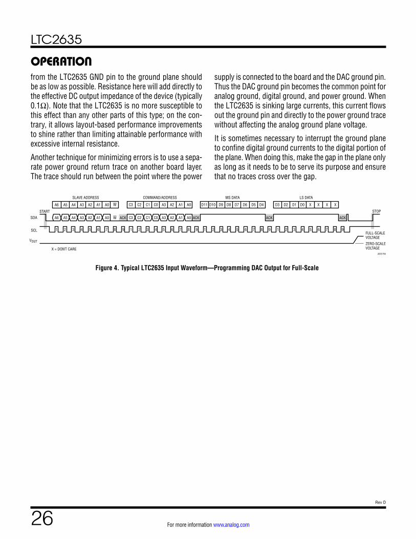
In any rail-to-rail voltage output device, the output is lim-ited to voltages within the supply range.
Since the analog output of the DAC cannot go below ground, it may limit for the lowest codes as shown in Figure 5b. Similarly, limiting can occur near full-scale when the REF pin is tied to VCC. If VREF = VCC and the DAC full-scale error (FSE) is positive, the output for the highest codes limits at VCC, as shown in Figure 5c. No full-scale limiting can occur if VREF is less than VCC – FSE.
Offset and linearity are defined and tested over the region of the DAC transfer function where no output limiting can occur.
Board Layout
The PC board should have separate areas for the analog and digital sections of the circuit. A single, solid ground plane should be used, with analog and digital signals care-fully routed over separate areas of the plane. This keeps digital signals away from sensitive analog signals and minimizes the interaction between digital ground currents and the analog section of the ground plane. The resistance
OPERATION
LTC2635
26Rev D
For more information www.analog.com
OPERATIONfrom the LTC2635 GND pin to the ground plane should be as low as possible. Resistance here will add directly to the effective DC output impedance of the device (typically 0.1Ω). Note that the LTC2635 is no more susceptible to this effect than any other parts of this type; on the con-trary, it allows layout-based performance improvements to shine rather than limiting attainable performance with excessive internal resistance.
Another technique for minimizing errors is to use a sepa-rate power ground return trace on another board layer. The trace should run between the point where the power
supply is connected to the board and the DAC ground pin. Thus the DAC ground pin becomes the common point for analog ground, digital ground, and power ground. When the LTC2635 is sinking large currents, this current flows out the ground pin and directly to the power ground trace without affecting the analog ground plane voltage.
It is sometimes necessary to interrupt the ground plane to confine digital ground currents to the digital portion of the plane. When doing this, make the gap in the plane only as long as it needs to be to serve its purpose and ensure that no traces cross over the gap.
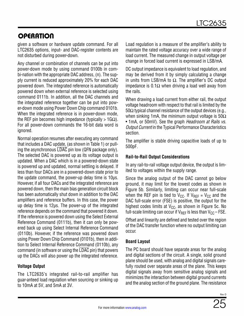
C3 C2 C1 C0 A3 A2 A1 A0
C3W
W
C2
COMMAND/ADDRESSSLAVE ADDRESS MS DATA LS DATA
C1 C0 A3 A2 A1 A0 D11 D10 D9 D8 D7 D6 D5 D4 D3
ACKACKACKACK
D2 D1 D0 X X X X
A0A1A2A3A4A5
1 2 3 4 5 6 7 8 9 1 2 3 4 5 6 7 8 9 1 2 3 4 5 6 7 8 9 1 2 3 4 5 6 7 8 9
A6
A0A1A2A3A4A5A6
START STOP
FULL-SCALEVOLTAGE
ZERO-SCALEVOLTAGE
SDA
SCL
VOUT
X = DON’T CARE2635 F04
Figure 4. Typical LTC2635 Input Waveform—Programming DAC Output for Full-Scale
LTC2635
27Rev D
For more information www.analog.com
Figure 5. Effects of Rail-to-Rail On a DAC Transfer Curve (Shown for 12 Bits). (a) Overall Transfer Function (b) Effect of Negative Offset for Codes Near Zero (c) Effect of Positive Full-Scale Error for Codes Near Full-Scale
2635 F05
INPUT CODE
(b)
(a)
(c)OUTPUTVOLTAGE
NEGATIVEOFFSET
0V
2,04800V
4,095INPUT CODE
OUTPUTVOLTAGE
VREF = VCC
VREF = VCC
INPUT CODE
OUTPUTVOLTAGE
POSITIVEFSE
OPERATION
LTC2635
28Rev D
For more information www.analog.com
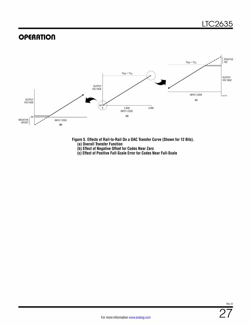
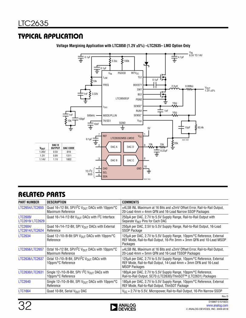
Voltage Margining Application with LTC3850 (1.2V ±5%) –LTC2635– LMO Option Only
APPLICATION INFORMATION
2635 TA02
0.1µF
5V
REF7
2
3
45TO I2C
BUS
2635 TA02
6
VCC
CAOSCLSDA
GND
LTC2635CMSE-LMOI2
DAC A
DAC B
DAC D
DAC C
1
9 10k 15k
0.22µF
10
8
BOOST1
TG1
SW1
BG1
PGND
SENSE+
RUN1
SENSE–
VFB1
PGOOD INTVCC
10Ω
10Ω
1nF
2.2µH 0.008Ω
VIN6.5V TO 14V
VOUT1.2V ±5%
MODE/PLLIN500kHz
FREQ
TK/SS1
ILIM
VIN
2.2Ω 100k
ITH1
10k
LTC3850EUF1nF 3.32k
1nF100pF
10k10nF
0.1µF
0.1µF
0.1µF
SGND
20k
4.7µF
15pF 63.4k
DAC D VOUT OUTPUT DAC CODE 1.26V 0.5V 819 1.2V 0.8V 1311 1.14V 1.1V 1802
LTC2635
29Rev D
For more information www.analog.com
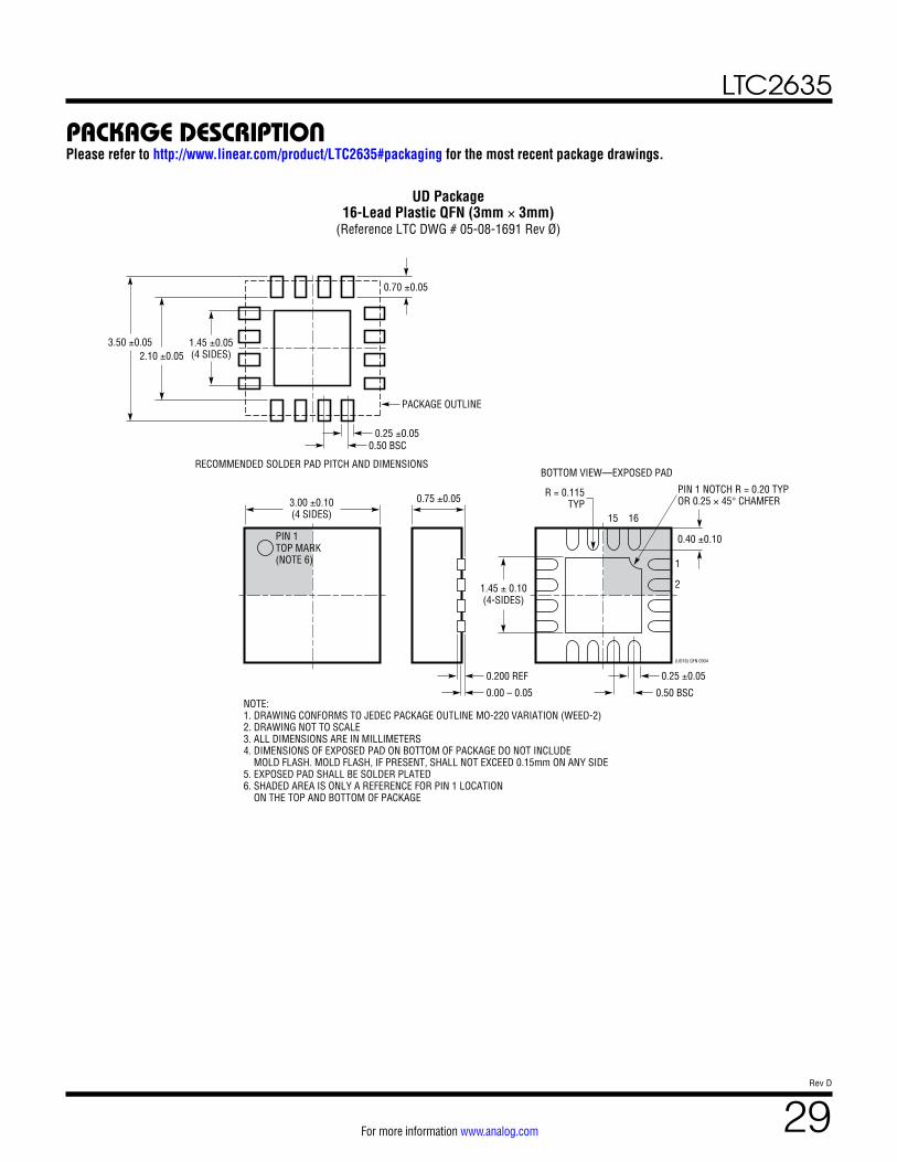
PACKAGE DESCRIPTION
3.00 ±0.10(4 SIDES)
RECOMMENDED SOLDER PAD PITCH AND DIMENSIONS
1.45 ±0.05(4 SIDES)
NOTE:1. DRAWING CONFORMS TO JEDEC PACKAGE OUTLINE MO-220 VARIATION (WEED-2)2. DRAWING NOT TO SCALE3. ALL DIMENSIONS ARE IN MILLIMETERS4. DIMENSIONS OF EXPOSED PAD ON BOTTOM OF PACKAGE DO NOT INCLUDE MOLD FLASH. MOLD FLASH, IF PRESENT, SHALL NOT EXCEED 0.15mm ON ANY SIDE5. EXPOSED PAD SHALL BE SOLDER PLATED6. SHADED AREA IS ONLY A REFERENCE FOR PIN 1 LOCATION ON THE TOP AND BOTTOM OF PACKAGE
PIN 1TOP MARK(NOTE 6)
0.40 ±0.10
BOTTOM VIEW—EXPOSED PAD
1.45 ± 0.10(4-SIDES)
0.75 ±0.05 R = 0.115TYP
0.25 ±0.05
1
PIN 1 NOTCH R = 0.20 TYPOR 0.25 × 45° CHAMFER
15 16
2
0.50 BSC
0.200 REF
2.10 ±0.053.50 ±0.05
0.70 ±0.05
0.00 – 0.05
(UD16) QFN 0904
0.25 ±0.050.50 BSC
PACKAGE OUTLINE
UD Package16-Lead Plastic QFN (3mm × 3mm)
(Reference LTC DWG # 05-08-1691 Rev Ø)
Please refer to http://www.linear.com/product/LTC2635#packaging for the most recent package drawings.
LTC2635
30Rev D
For more information www.analog.com
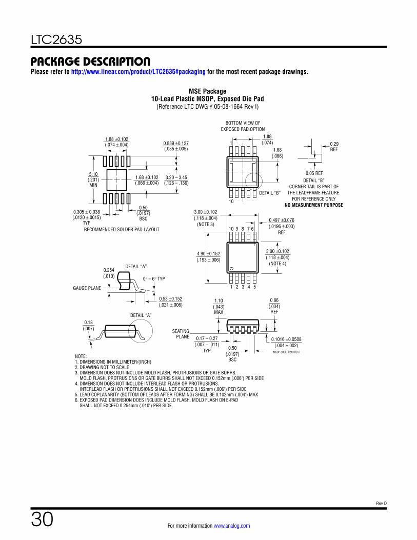
PACKAGE DESCRIPTION
MSOP (MSE) 0213 REV I
0.53 ±0.152(.021 ±.006)
SEATINGPLANE
0.18(.007)
1.10(.043)MAX
0.17 – 0.27(.007 – .011)
TYP
0.86(.034)REF
0.50(.0197)
BSC
1 2 3 4 5
4.90 ±0.152(.193 ±.006)
0.497 ±0.076(.0196 ±.003)
REF8910
10
1
7 6
3.00 ±0.102(.118 ±.004)
(NOTE 3)
3.00 ±0.102(.118 ±.004)
(NOTE 4)
NOTE:1. DIMENSIONS IN MILLIMETER/(INCH)2. DRAWING NOT TO SCALE3. DIMENSION DOES NOT INCLUDE MOLD FLASH, PROTRUSIONS OR GATE BURRS. MOLD FLASH, PROTRUSIONS OR GATE BURRS SHALL NOT EXCEED 0.152mm (.006") PER SIDE4. DIMENSION DOES NOT INCLUDE INTERLEAD FLASH OR PROTRUSIONS. INTERLEAD FLASH OR PROTRUSIONS SHALL NOT EXCEED 0.152mm (.006") PER SIDE5. LEAD COPLANARITY (BOTTOM OF LEADS AFTER FORMING) SHALL BE 0.102mm (.004") MAX6. EXPOSED PAD DIMENSION DOES INCLUDE MOLD FLASH. MOLD FLASH ON E-PAD SHALL NOT EXCEED 0.254mm (.010") PER SIDE.
0.254(.010) 0° – 6° TYP
DETAIL “A”
DETAIL “A”
GAUGE PLANE
5.10(.201)MIN
3.20 – 3.45(.126 – .136)
0.889 ±0.127(.035 ±.005)
RECOMMENDED SOLDER PAD LAYOUT
1.68 ±0.102(.066 ±.004)
1.88 ±0.102(.074 ±.004)
0.50(.0197)
BSC0.305 ± 0.038(.0120 ±.0015)
TYP
BOTTOM VIEW OFEXPOSED PAD OPTION
1.68(.066)
1.88(.074)
0.1016 ±0.0508(.004 ±.002)
DETAIL “B”
DETAIL “B”CORNER TAIL IS PART OF
THE LEADFRAME FEATURE.FOR REFERENCE ONLY
NO MEASUREMENT PURPOSE
0.05 REF
0.29REF
MSE Package10-Lead Plastic MSOP, Exposed Die Pad
(Reference LTC DWG # 05-08-1664 Rev I)
Please refer to http://www.linear.com/product/LTC2635#packaging for the most recent package drawings.
LTC2635
31Rev D
For more information www.analog.com
Information furnished by Analog Devices is believed to be accurate and reliable. However, no responsibility is assumed by Analog Devices for its use, nor for any infringements of patents or other rights of third parties that may result from its use. Specifications subject to change without notice. No license is granted by implication or otherwise under any patent or patent rights of Analog Devices.
REV DATE DESCRIPTION PAGE NUMBER
A 12/09 Revise QFN pin names.Minor text edit in Operations section.
2, 1721, 24
B 06/10 Revised Note 3 in the Electrical Characteristics section.Added Typical Application drawing and revised Related Parts List.
1132
C 05/17 Corrected VCC slew rate requirement when operating above 90°C and with VCC > 4V. 11
D 04/18 Edits to Note 3. 11
REVISION HISTORY
LTC2635
32Rev D
For more information www.analog.com ANALOG DEVICES, INC. 2009-2018
D16867-0-5/18(D)www.analog.com
RELATED PARTS
Voltage Margining Application with LTC3850 (1.2V ±5%) –LTC2635– LMO Option Only
TYPICAL APPLICATION
2635 TA020.1µF
5V
REF7
2
3
45TO I2C
BUS
2635 TA03
6
VCC
CAOSCLSDA
GND
LTC2635CMSE-LMOI2
DAC A
DAC B
DAC D
DAC C
1
9 10k 15k
0.22µF
10
8
BOOST1
TG1
SW1
BG1
PGND
SENSE+
RUN1
SENSE–
VFB1
PGOOD INTVCC
10Ω
10Ω1nF
2.2µH 0.008Ω
VIN6.5V TO 14V
VOUT1.2V ±5%
MODE/PLLIN500kHz
FREQ
TK/SS1
ILIM
VIN
2.2Ω 100k
ITH1
10k
LTC3850EUF
1nF 3.32k
1nF100pF
10k10nF
0.1µF
0.1µF
0.1µF
SGND
20k
4.7µF
15pF 63.4k
DAC D VOUT OUTPUT DAC CODE 1.26V 0.5V 819 1.2V 0.8V 1311 1.14V 1.1V 1802
PART NUMBER DESCRIPTION COMMENTSLTC2654/LTC2655 Quad 16-/12 Bit, SPI/I2C VOUT DACs with 10ppm/°C
Maximum Reference±4LSB INL Maximum at 16 Bits and ±2mV Offset Error, Rail-to-Rail Output, 20-Lead 4mm × 4mm QFN and 16-Lead Narrow SSOP Packages
LTC2609/LTC2619/ LTC2629
Quad 16-/14-/12-Bit VOUT DACs with I2C Interface 250µA per DAC, 2.7V to 5.5V Supply Range, Rail-to-Rail Output with Separate VREF Pins for Each DAC
LTC2604/LTC2614/LTC2624
Quad 16-/14-/12-Bit, SPI VOUT DACs with External Reference
250µA per DAC, 2.5V to 5.5V Supply Range, Rail-to-Rail Output, 16-Lead SSOP Package
LTC2634 Quad 12-/10-/8-Bit SPI VOUT DACs with 10ppm/°C Reference
125µA per DAC, 2.7V to 5.5V Supply Range, 10ppm/°C Reference, External REF Mode, Rail-to-Rail Output, 16-Pin 3mm × 3mm QFN and 10-Lead MSOP Packages
LTC2656/LTC2657 Octal 16-/12 Bit, SPI/I2C VOUT DACs with 10ppm/°C Maximum Reference
±4LSB INL Maximum at 16 Bits and ±2mV Offset Error, Rail-to-Rail Output, 20-Lead 4mm × 5mm QFN and 16-Lead TSSOP Packages
LTC2636/LTC2637 Octal 12-/10-/8-Bit, SPI/I2C VOUT DACs with 10ppm/°C Reference
125µA per DAC, 2.7V to 5.5V Supply Range, 10ppm/°C Reference, External REF Mode, Rail-to-Rail Output, 14-Lead 4mm × 3mm DFN and 16-Lead MSOP Packages
LTC2630/LTC2631 Single 12-/10-/8-Bit, SPI/ I2C VOUT DACs with 10ppm/°C Reference
180µA per DAC, 2.7V to 5.5V Supply Range, 10ppm/°C Reference, Rail-to-Rail Output, SC70 (LTC2630)/ThinSOT™ (LTC2631) Packages
LTC2640 Single 12-/10-/8-Bit, SPI VOUT DACs with 10ppm/°C Reference
180µA per DAC, 2.7V to 5.5V Supply Range, 10ppm/°C Reference, External REF Mode, Rail-to-Rail Output, ThinSOT Package
LTC1664 Quad 10-Bit, Serial VOUT DAC VCC = 2.7V to 5.5V, Micropower, Rail-to-Rail Output, 16-Pin Narrow SSOP


![- -r · rB UP q; //0 LA,' /-\ by P /P( 1 r--X. 7< rD =••q• > T)a g IF\$ \r V\ r a A) rb P > \V (FJ \n (IP. J J rr–b) I rx-I VJ r-b)]D (''](https://static.fdocuments.us/doc/165x107/6003daa0c13a8819f8274e30/-r-rb-up-q-0-la-by-p-p-1-r-x-7-rd-aaqa-ta-g-if-r.jpg)