
LT3845A
26
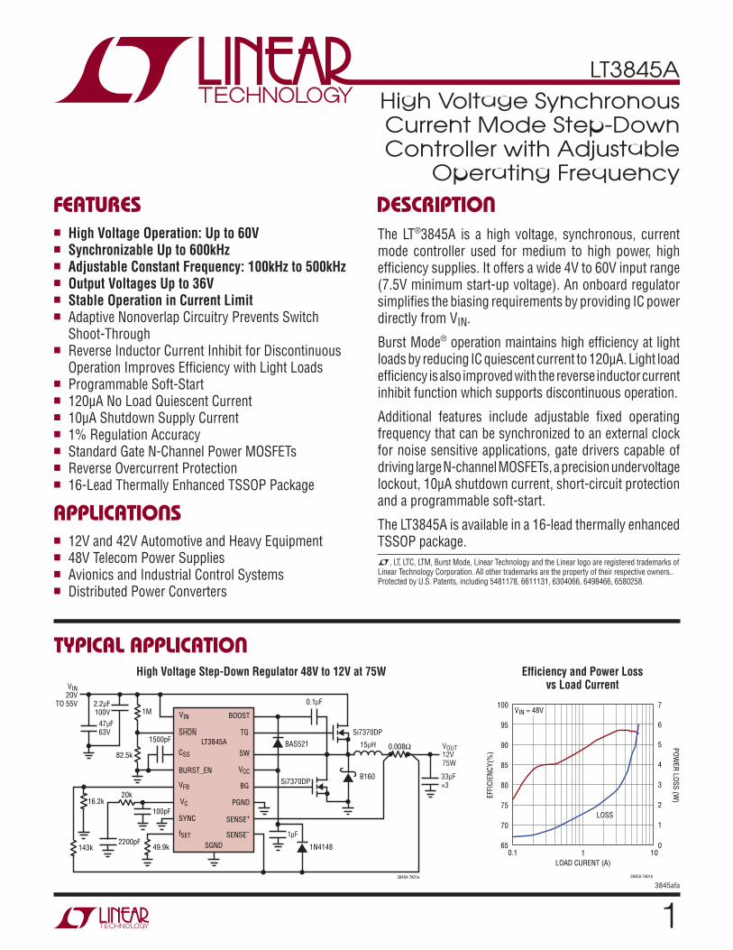
LT3845A 1 3845afa TYPICAL APPLICATION FEATURES APPLICATIONS DESCRIPTION High Voltage Synchronous Current Mode Step-Down Controller with Adjustable Operating Frequency The LT ® 3845A is a high voltage, synchronous, current mode controller used for medium to high power, high efficiency supplies. It offers a wide 4V to 60V input range (7.5V minimum start-up voltage). An onboard regulator simplifies the biasing requirements by providing IC power directly from V IN . Burst Mode ® operation maintains high efficiency at light loads by reducing IC quiescent current to 120µA. Light load efficiency is also improved with the reverse inductor current inhibit function which supports discontinuous operation. Additional features include adjustable fixed operating frequency that can be synchronized to an external clock for noise sensitive applications, gate drivers capable of driving large N-channel MOSFETs, a precision undervoltage lockout, 10µA shutdown current, short-circuit protection and a programmable soft-start. The LT3845A is available in a 16-lead thermally enhanced TSSOP package. n High Voltage Operation: Up to 60V n Synchronizable Up to 600kHz n Adjustable Constant Frequency: 100kHz to 500kHz n Output Voltages Up to 36V n Stable Operation in Current Limit n Adaptive Nonoverlap Circuitry Prevents Switch Shoot-Through n Reverse Inductor Current Inhibit for Discontinuous Operation Improves Efficiency with Light Loads n Programmable Soft-Start n 120µA No Load Quiescent Current n 10µA Shutdown Supply Current n 1% Regulation Accuracy n Standard Gate N-Channel Power MOSFETs n Reverse Overcurrent Protection n 16-Lead Thermally Enhanced TSSOP Package n 12V and 42V Automotive and Heavy Equipment n 48V Telecom Power Supplies n Avionics and Industrial Control Systems n Distributed Power Converters High Voltage Step-Down Regulator 48V to 12V at 75W L, LT, LTC, LTM, Burst Mode, Linear Technology and the Linear logo are registered trademarks of Linear Technology Corporation. All other trademarks are the property of their respective owners.. Protected by U.S. Patents, including 5481178, 6611131, 6304066, 6498466, 6580258. SGND BAS521 1N4148 3845A TA01a 0.1μF 1500pF Si7370DP Si7370DP B160 15μH 0.008Ω LT3845A 1μF 33μF ×3 V OUT 12V 75W 1M 82.5k 16.2k V IN 20V TO 55V 2.2μF 100V 49.9k 20k 100pF 2200pF 143k 47μF 63V BOOST TG SW V CC BG PGND SENSE + SENSE – V IN SHDN C SS BURST_EN V FB V C SYNC f SET Efficiency and Power Loss vs Load Current LOAD CURENT (A) 65 80 75 70 100 95 90 85 0 3 2 1 7 6 5 4 3845A TA01b EFFICIENCY(%) POWER LOSS (W) 0.1 10 1 V IN = 48V LOSS
Transcript of LT3845A
LT3845A
13845afa
TYPICAL APPLICATION
FEATURES
APPLICATIONS
DESCRIPTION
High Voltage SynchronousCurrent Mode Step-Down Controller with Adjustable
Operating Frequency
The LT®3845A is a high voltage, synchronous, current mode controller used for medium to high power, high efficiency supplies. It offers a wide 4V to 60V input range (7.5V minimum start-up voltage). An onboard regulator simplifies the biasing requirements by providing IC power directly from VIN.
Burst Mode® operation maintains high efficiency at light loads by reducing IC quiescent current to 120µA. Light load efficiency is also improved with the reverse inductor current inhibit function which supports discontinuous operation.
Additional features include adjustable fixed operating frequency that can be synchronized to an external clock for noise sensitive applications, gate drivers capable of driving large N-channel MOSFETs, a precision undervoltage lockout, 10µA shutdown current, short-circuit protection and a programmable soft-start.
The LT3845A is available in a 16-lead thermally enhanced TSSOP package.
n High Voltage Operation: Up to 60Vn Synchronizable Up to 600kHzn Adjustable Constant Frequency: 100kHz to 500kHzn Output Voltages Up to 36Vn Stable Operation in Current Limitn Adaptive Nonoverlap Circuitry Prevents Switch
Shoot-Throughn Reverse Inductor Current Inhibit for Discontinuous
Operation Improves Efficiency with Light Loadsn Programmable Soft-Startn 120µA No Load Quiescent Currentn 10µA Shutdown Supply Currentn 1% Regulation Accuracyn Standard Gate N-Channel Power MOSFETsn Reverse Overcurrent Protectionn 16-Lead Thermally Enhanced TSSOP Package
n 12V and 42V Automotive and Heavy Equipmentn 48V Telecom Power Suppliesn Avionics and Industrial Control Systemsn Distributed Power Converters
High Voltage Step-Down Regulator 48V to 12V at 75W
L, LT, LTC, LTM, Burst Mode, Linear Technology and the Linear logo are registered trademarks of Linear Technology Corporation. All other trademarks are the property of their respective owners.. Protected by U.S. Patents, including 5481178, 6611131, 6304066, 6498466, 6580258.
SGND
BAS521
1N4148
3845A TA01a
0.1µF
1500pFSi7370DP
Si7370DPB160
15µH 0.008ΩLT3845A
1µF
33µF×3
VOUT12V75W
1M
82.5k
16.2k
VIN20V
TO 55V 2.2µF100V
49.9k
20k
100pF
2200pF143k
47µF63V
BOOST
TG
SW
VCC
BG
PGND
SENSE+
SENSE–
VIN
SHDN
CSS
BURST_EN
VFB
VC
SYNC
fSET
Efficiency and Power Loss vs Load Current
LOAD CURENT (A)
65
80
75
70
100
95
90
85
0
3
2
1
7
6
5
4
3845A TA01b
EFFI
CIEN
CY(%
)
POWER LOSS (W
)
0.1 101
VIN = 48V
LOSS
LT3845A
23845afa
ORDER INFORMATION
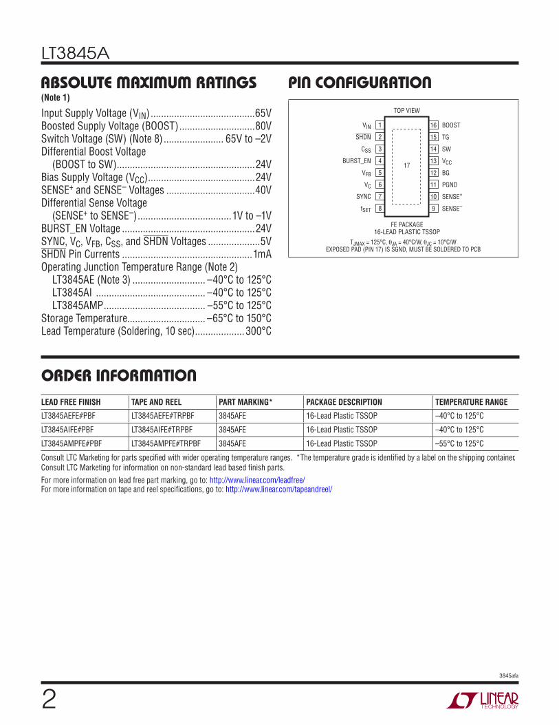
ABSOLUTE MAXIMUM RATINGS(Note 1)
Input Supply Voltage (VIN) ........................................65V Boosted Supply Voltage (BOOST) .............................80VSwitch Voltage (SW) (Note 8) ....................... 65V to –2V Differential Boost Voltage (BOOST to SW) .....................................................24VBias Supply Voltage (VCC) .........................................24VSENSE+ and SENSE– Voltages ..................................40VDifferential Sense Voltage (SENSE+ to SENSE–) ....................................1V to –1V BURST_EN Voltage ...................................................24VSYNC, VC, VFB, CSS, and SHDN Voltages ....................5VSHDN Pin Currents ..................................................1mAOperating Junction Temperature Range (Note 2) LT3845AE (Note 3) ............................ –40°C to 125°C LT3845AI .......................................... –40°C to 125°C LT3845AMP ....................................... –55°C to 125°CStorage Temperature.............................. –65°C to 150°CLead Temperature (Soldering, 10 sec) ................... 300°C
LEAD FREE FINISH TAPE AND REEL PART MARKING* PACKAGE DESCRIPTION TEMPERATURE RANGE
LT3845AEFE#PBF LT3845AEFE#TRPBF 3845AFE 16-Lead Plastic TSSOP –40°C to 125°C
LT3845AIFE#PBF LT3845AIFE#TRPBF 3845AFE 16-Lead Plastic TSSOP –40°C to 125°C
LT3845AMPFE#PBF LT3845AMPFE#TRPBF 3845AFE 16-Lead Plastic TSSOP –55°C to 125°C
Consult LTC Marketing for parts specified with wider operating temperature ranges. *The temperature grade is identified by a label on the shipping container.Consult LTC Marketing for information on non-standard lead based finish parts.For more information on lead free part marking, go to: http://www.linear.com/leadfree/ For more information on tape and reel specifications, go to: http://www.linear.com/tapeandreel/
FE PACKAGE16-LEAD PLASTIC TSSOP
1
2
3
4
5
6
7
8
TOP VIEW
16
15
14
13
12
11
10
9
VIN
SHDN
CSS
BURST_EN
VFB
VC
SYNC
fSET
BOOST
TG
SW
VCC
BG
PGND
SENSE+
SENSE–
17
TJMAX = 125°C, qJA = 40°C/W, qJC = 10°C/W
EXPOSED PAD (PIN 17) IS SGND, MUST BE SOLDERED TO PCB
PIN CONFIGURATION
LT3845A
33845afa
PARAMETER CONDITIONS MIN TYP MAX UNITS
VIN Operating Voltage Range (Note 4) VIN Minimum Start Voltage VIN UVLO Threshold (Falling) VIN UVLO Threshold Hysteresis
l
l
l
4
3.6
3.8 670
60 7.5 4
V V V
mV
VIN Supply Current VIN Burst Mode Current VIN Shutdown Current
VCC > 9V VBURST_EN = 0V, VFB = 1.35V VSHDN = 0V
l
20 20 9
15
µA µA µA
BOOST Operating Voltage Range BOOST Operating Voltage Range (Note 5) BOOST UVLO Threshold (Rising) BOOST UVLO Threshold Hysteresis
VBOOST – VSW VBOOST – VSW VBOOST – VSW
l
l
5
400
75 20
V V V
mV
BOOST Supply Current (Note 6) BOOST Burst Mode Current BOOST Shutdown Current
VBURST_EN = 0V VSHDN = 0V
1.4 0.1 0.1
mA µA µA
VCC Operating Voltage Range (Note 5) VCC Output Voltage VCC UVLO Threshold (Rising) VCC UVLO Threshold Hysteresis
Over Full Line and Load Range
l
l
8
6.25 500
20 8.3
V V V
mV
VCC Supply Current (Note 6) VCC Burst Mode Current VCC Shutdown Current VCC Current Limit
VBURST_EN = 0V VSHDN = 0V
l
l
–40
3 100 20
–150
3.7 mA µA µA
mA
Error Amp Reference Voltage Measured at VFB Pin
l
1.224 1.215
1.231 1.238 1.245
V V
VFB Pin Input Current VFB = 1.231V 25 nA
SHDN Enable Threshold (Rising) SHDN Threshold Hysteresis
l 1.3 1.35 120
1.4 V mV
Sense Pins Common Mode Range Current Limit Sense Voltage Reverse Protect Sense Voltage Reverse Current Inhibit Offset
VSENSE
+ – VSENSE–
VSENSE+ – VSENSE
–, VBURST_EN = VCC VBURST_EN = 0V or VBURST_EN = VFB
l
l
0 90
100
–100 10
36 115
V mV mV mV
Input Current (ISENSE+ + ISENSE
–) VSENSE(CM) = 0V VSENSE(CM) = 2V VSENSE(CM) > 4V
800 –20
–300
µA µA µA
Operating Frequency l 270 300 330 kHz
Minimum Programmable Frequency Maximum Programmable Frequency
l
l
500
100 kHz kHz
External Sync Frequency Range l 100 600 kHz
SYNC Input Resistance 40 kΩ
SYNC Voltage Threshold l 1.4 2 V
Soft-Start Capacitor Control Current 2 µA
Error Amp Transconductance l 270 340 410 µS
Error Amp DC Voltage Gain 62 dB
Error Amp Sink/Source Current ±30 µA
ELECTRICAL CHARACTERISTICS The l denotes the specifications which apply over the full operating temperature range, otherwise specifications are at TA = 25°C. VIN = 20V, VCC = BOOST = BURST_EN = 10V, SHDN = 2V, RSET = 49.9kΩ, SENSE– = SENSE+ = 10V, SGND = PGND = SW = SYNC = 0V, unless otherwise noted.
LT3845A
43845afa
Note 1: Stresses beyond those listed under Absolute Maximum Ratings may cause permanent damage to the device. Exposure to any Absolute Maximum Rating condition for extended periods may affect device reliability and lifetime.Note 2: The LT3845A includes overtemperature protection that is intended to protect the device during momentary overload conditions. Junction temperature will exceed 125°C when overtemperature protection is active. Continuous operation above the specified maximum operating junction temperature may impair device reliability.Note 3: The LT3845AE is guaranteed to meet performance specifications from 0°C to 125°C junction temperature. Specifications over the –40°C to 125°C operating junction temperature range are assured by design, characterization and correlation with statistical process controls. The LT3845AI is guaranteed over the full –40°C to 125°C operating junction temperature range. The LT3845AMP is 100% tested and guaranteed over the –55°C to 125°C temperature range.
Note 4: VIN voltages below the start-up threshold (7.5V) are only supported when the VCC is externally driven above 6.5V.Note 5: Operating range is dictated by MOSFET absolute maximum VGS.Note 6: Supply current specification does not include switch drive currents. Actual supply currents will be higher.Note 7: DC measurement of gate drive output “ON” voltage is typically 8.6V. Internal dynamic bootstrap operation yields typical gate “ON” voltages of 9.8V during standard switching operation. Standard operation gate “ON” voltage is not tested but guaranteed by design.Note 8: The –2V absolute maximum on the SW pin is a transient condition. It is guaranteed by design and not subject to test.
ELECTRICAL CHARACTERISTICS The l denotes the specifications which apply over the full operating temperature range, otherwise specifications are at TA = 25°C. VIN = 20V, VCC = BOOST = BURST_EN = 10V, SHDN = 2V, RSET = 49.9kΩ, SENSE– = SENSE+ = 10V, SGND = PGND = SW = SYNC = 0V, unless otherwise noted.
PARAMETER CONDITIONS MIN TYP MAX UNITS
TG, BG Drive On Voltage (Note 7) TG, BG Drive Off Voltage
CLOAD = 3300pF CLOAD = 3300pF
9.8 0.1
V V
TG, BG Drive Rise/Fall Time 10% to 90% or 90% to 10%, CLOAD = 3300pF 50 ns
Minimum TG Off Time l 350 650 ns
Minimum TG On Time l 250 400 ns
Gate Drive Nonoverlap Time TG Fall to BG Rise BG Fall to TG Rise
200 150
ns ns
LT3845A
53845afa
Shutdown Threshold (Rising) vs Temperature VCC vs Temperature
VCC vs ICC(LOAD) ICC Current Limit vs Temperature
VCC UVLO Threshold (Rising) vs Temperature ICC vs VCC (SHDN = 0V)
Error Amp Transconductance vs Temperature
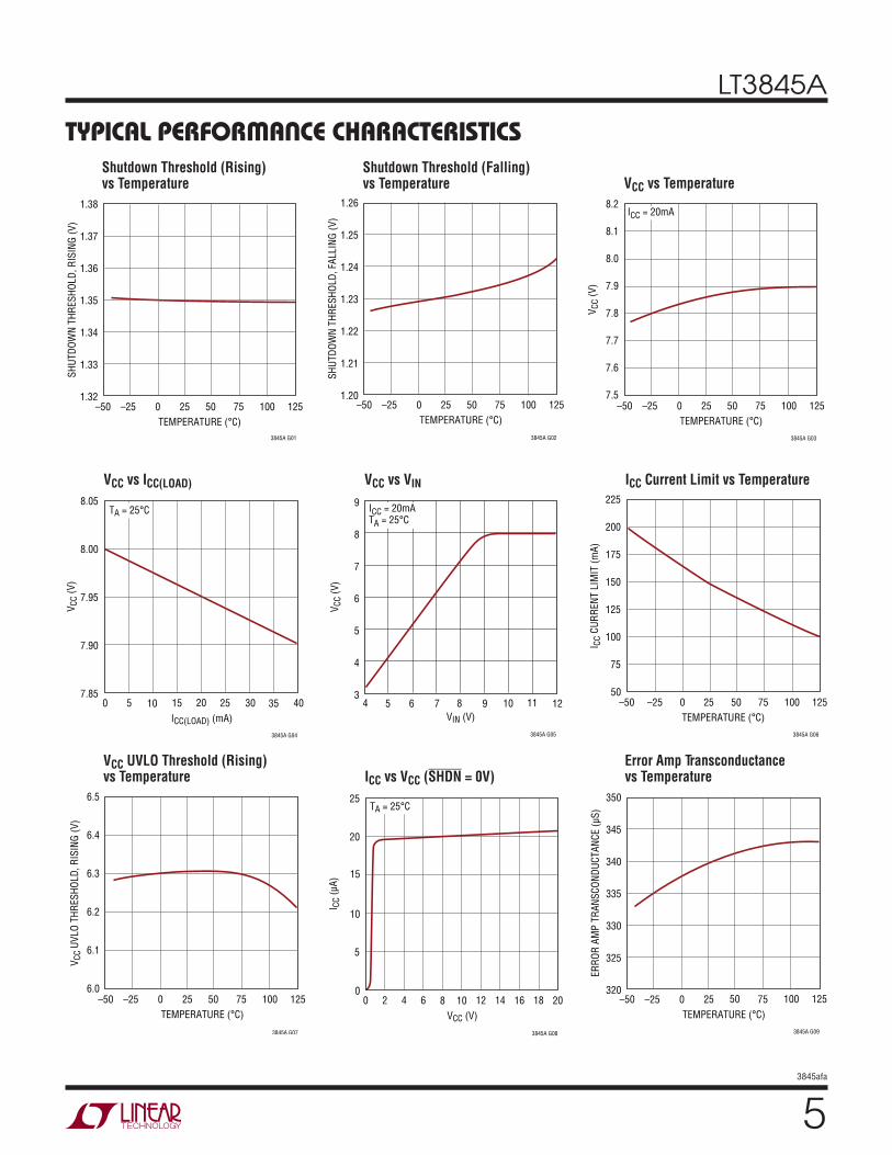
TYPICAL PERFORMANCE CHARACTERISTICS
3845A G01
SHUT
DOW
N TH
RESH
OLD,
RIS
ING
(V)
1.38
1.37
1.36
1.35
1.34
1.33
1.32
TEMPERATURE (°C)–50 25 75–25 0 50 100 125
Shutdown Threshold (Falling) vs Temperature
3845A G02
TEMPERATURE (°C)–50
SHUT
DOW
N TH
RESH
OLD,
FAL
LING
(V)
1.26
1.25
1.24
1.23
1.22
1.21
1.2025 75–25 0 50 100 125
TEMPERATURE (°C)–50 25 75–25 0 50 100 125
3845A G03
8.2
8.1
8.0
7.9
7.8
7.7
7.6
7.5
V CC
(V)
ICC = 20mA
ICC(LOAD) (mA)0
V CC
(V)
40
3845A G04
10 20 30
8.05
8.00
7.95
7.90
7.855 15 25 35
TA = 25°C
VCC vs VIN
3845A G05
VIN (V)
V CC
(V)
9
8
7
6
5
4
34 6 8 95 7 10 11 12
ICC = 20mATA = 25°C
–50 –25 1000 50 12525 75TEMPERATURE (°C)
225
200
175
150
125
100
75
50
3845A G06
I CC
CURR
ENT
LIM
IT (m
A)
3845A G07
TEMPERATURE (°C)–50 25 75–25 0 50 100 125
V CC
UVLO
THR
ESHO
LD, R
ISIN
G (V
)
6.5
6.4
6.3
6.2
6.1
6.0
3845A G08
VCC (V)0
I CC
(µA)
15
20
25
16
10
5
02 4 6 8 10 12 14 18 20
TA = 25°C
TEMPERATURE (°C)–50
ERRO
R AM
P TR
ANSC
ONDU
CTAN
CE (µ
S)
350
345
340
335
330
325
32025 75
3845A G09
–25 0 50 100 125
LT3845A
63845afa
Maximum Current Sense Threshold vs Temperature
TEMPERATURE (°C)–50
CURR
ENT
SENS
E TH
RESH
OLD
(mV)
102
104
106
25 75
3845A G13
100
98
–25 0 50 100 125
96
94
VIN UVLO Threshold (Rising) vs Temperature
TEMPERATURE (°C)–50 25 75–25 0 50 100 125
3845A G14
4.54
4.52
4.50
4.48
4.46
4.44
4.42
4.40
V IN
UVLO
THR
ESHO
LD, R
ISIN
G (V
)
VIN UVLO Threshold (Falling) vs Temperature
TEMPERATURE (°C)–50 25 75–25 0 50 100 125
3845A G15
V IN
UVLO
THR
ESHO
LD, F
ALLI
NG (V
)
3.86
3.84
3.82
3.80
3.78
3.76
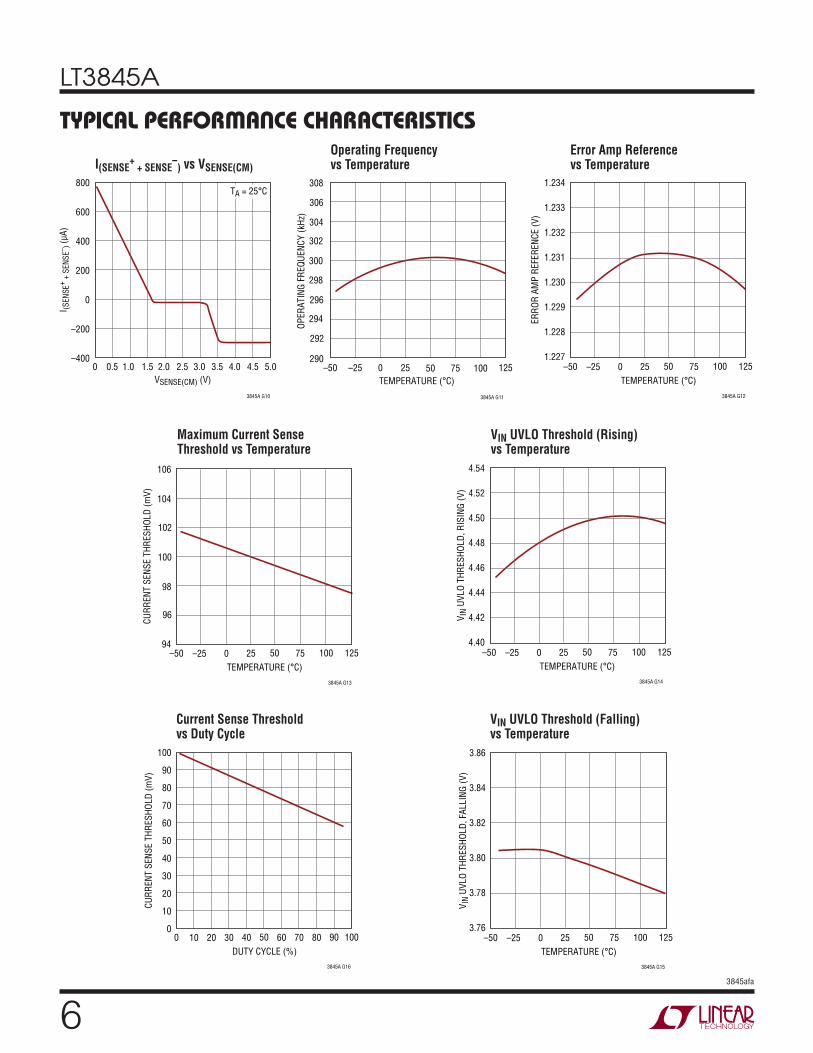
TYPICAL PERFORMANCE CHARACTERISTICS
I(SENSE+
+ SENSE–
) vs VSENSE(CM)
Operating Frequency vs Temperature
VSENSE(CM) (V)0 0.5 1.5 2.5 3.5 4.5
I (SEN
SE+ +
SEN
SE– ) (
µA)
800
600
400
200
0
–200
–4001.0 2.0 3.0 4.0
3845A G10
5.0
TA = 25°C
TEMPERATURE (°C)–50
290
OPER
ATIN
G FR
EQUE
NCY
(kHz
)
292
296
298
300
50
308
3845A G11
294
0–25 75 10025 125
302
304
306
TEMPERATURE (°C)–50 25 75
3845A G12
–25 0 50 100 125
1.234
1.233
1.232
1.231
1.230
1.229
1.228
1.227
ERRO
R AM
P RE
FERE
NCE
(V)
Error Amp Reference vs Temperature
DUTY CYCLE (%)0 40 60 70 8010 20 30 50 90 100
3845A G16
CURR
ENT
SENS
E TH
RESH
OLD
(mV)
0
10
20
30
40
50
60
70
80
90
100
Current Sense Threshold vs Duty Cycle
LT3845A
73845afa
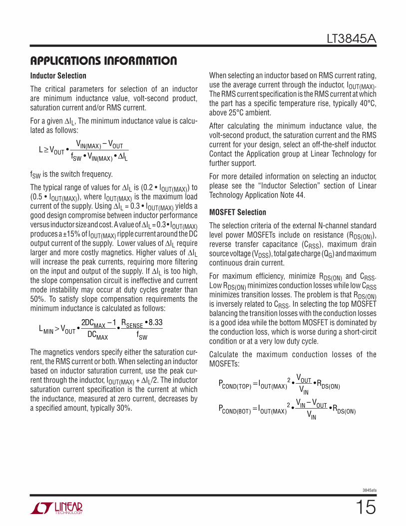
BG: The BG pin is the gate drive for the bottom N-channel MOSFET. Since very fast high currents are driven from this pin, connect it to the gate of the power MOSFET with a short and wide, typically 0.02" width, PCB trace to minimize inductance.
BOOST: The BOOST pin is the supply for the bootstrapped gate drive and is externally connected to a low ESR ceramic boost capacitor referenced to SW pin. The recommended value of the BOOST capacitor, CBOOST, is at least 50 times greater than the total gate capacitance of the topside MOSFET. In most applications 0.1µF is adequate. The maximum voltage that this pin sees is VIN + VCC, ground referred.
BURST_EN: Burst Mode Operation Enable Pin. This pin also controls reverse-current inhibit mode of operation. When the pin voltage is below 0.5V, Burst Mode operation and reverse-current inhibit functions are enabled. When the pin voltage is above 0.5V, Burst Mode operation is disabled, but reverse-current inhibit operation is maintained. In this mode of operation (BURST_EN = VFB) there is a 1mA minimum load requirement. Reverse-current inhibit is disabled when the pin voltage is above 2.5V. This pin is typically shorted to ground to enable Burst Mode operation and reverse-current inhibit, shorted to VFB to disable Burst Mode operation while enabling reverse-current inhibit, and connected to VCC pin to disable both functions. See Applications Information section.
CSS: The soft-start pin is used to program the supply soft-start function. Use the following formula to calculate CSS for a given output voltage slew rate:
CSS = 2µA(tSS/1.231V)
The pin should be left unconnected when not using the soft-start function.
fSET: The fSET pin programs the oscillator frequency with an external resistor, RSET. The resistor is required even when supplying external sync clock signal. See the Applications Information section for resistor value selection details.
PGND: The PGND pin is the high-current ground reference for internal low side switch driver and the VCC regulator circuit. Connect the pin directly to the negative terminal of the VCC decoupling capacitor. See the Application Information section for helpful hints on PCB layout of grounds.
SENSE–: The SENSE– pin is the negative input for the current sense amplifier and is connected to the VOUT side of the sense resistor for step-down applications.
SENSE+: The SENSE+ pin is the positive input for the current sense amplifier and is connected to the inductor side of the sense resistor for step-down applications.
SGND: The SGND pin is the low noise ground reference. It should be connected to the –VOUT side of the output capacitors. Careful layout of the PCB is necessary to keep high currents away from this SGND connection. See the Application Information section for helpful hints on PCB layout of grounds.
SHDN: The SHDN pin has a precision IC enable threshold of 1.35V (rising) with 120mV of hysteresis. It is used to implement an undervoltage lockout (UVLO) circuit. See Application Information section for implementing a UVLO function. When the SHDN pin is pulled below a transistor VBE (0.7V), a low current shutdown mode is entered, all internal circuitry is disabled and the VIN supply current is reduced to approximately 9µA. Typical pin input bias current is <10nA and the pin is internally clamped to 6V. If the function is not used, this pin may be tied to VIN through a high value resistor.
SW: Reference for VBOOST Supply and High Current Return for Bootstrapped Switch.
SYNC: The Sync pin provides an external clock input for synchronization of the internal oscillator. RSET is set such that the internal oscillator frequency is 10% to 25% below the external clock frequency. If unused the Sync pin is connected to SGND. For more information see “Oscillator Sync” in the Application Information section of this data sheet. Sync pin not available in PDIP package.
PIN FUNCTIONS
LT3845A
83845afa
TG: The TG pin is the bootstrapped gate drive for the top N-Channel MOSFET. Since very fast high currents are driven from this pin, connect it to the gate of the power MOSFET with a short and wide, typically 0.02” width, PCB trace to minimize inductance.
VC: The VC pin is the output of the error amplifier whose voltage corresponds to the maximum (peak) switch current per oscillator cycle. The error amplifier is typically configured as an integrator by connecting an RC network from the VC pin to SGND. This circuit creates the dominant pole for the converter regulation control loop. Specific integrator characteristics can be configured to optimize transient response. When Burst Mode operation is enabled (see Pin 4 description), an internal low impedance clamp on the VC pin is set at 100mV below the burst threshold, which limits the negative excursion of the pin voltage. Therefore, this pin cannot be pulled low with a low impedance source. If the VC pin must be externally manipulated, do so through a 1kΩ series resistance.
VCC: The VCC pin is the internal bias supply decoupling node. Use a low ESR, 1µF or greater ceramic capacitor to decouple this node to PGND. Most internal IC functions are
PIN FUNCTIONSpowered from this bias supply. An external diode connected from VCC to the BOOST pin charges the bootstrapped capacitor during the off-time of the main power switch. Back driving the VCC pin from an external DC voltage source, such as the VOUT output of the regulator supply, increases overall efficiency and reduces power dissipation in the IC. In shutdown mode this pin sinks 20µA until the pin voltage is discharged to 0V.
VFB: The output voltage feedback pin, VFB, is externally connected to the supply output voltage via a resistive divider. The VFB pin is internally connected to the inverting input of the error amplifier. In regulation, VFB is 1.231V.
VIN: The VIN pin is the main supply pin and should be decoupled to SGND with a low ESR capacitor (at least 0.1µF) located close to the pin.
Exposed Pad (SGND) (TSSOP Only): The exposed leadframe is internally connected to the SGND pin. Solder the exposed pad to the PCB ground for electrical contact and optimal thermal performance.
LT3845A
93845afa
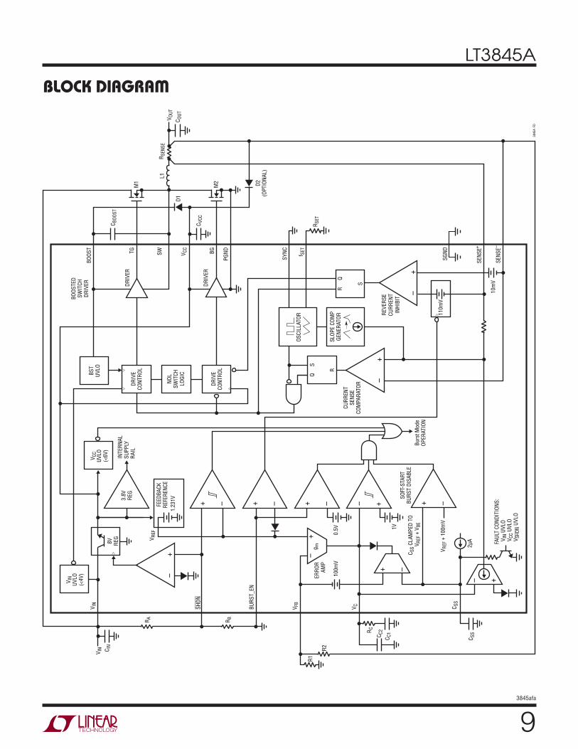
BLOCK DIAGRAM
–+
–+
–+ –+–+
V IN
UVLO
(<4V
)
BST
UVLO
8V REG
FEED
BACK
REFE
RENC
E
– +
1.23
1V3.8V
REG
INTE
RNAL
SUPP
LYRA
IL
V IN
V CC
UVLO
(<6V
)
SHDN
V REF
DRIV
ECO
NTRO
L
NOL
SWIT
CHLO
GIC
DRIV
ECO
NTRO
L
BURS
T_EN
R B
V C C SS
SENS
E–
V FB
–+
V REF
+ 1
00m
V
FAUL
T CO
NDIT
IONS
: V
IN U
VLO
VCC
UVL
O V
SHDN
UVL
O
2µA
1V
0.5V
100m
V
ERRO
RAM
P
Burs
t Mod
eOP
ERAT
ION
SOFT
-STA
RTBU
RST
DISA
BLE
C SS
CLAM
PED
TO
V REF
+ V
BE
R
SQ
OSCI
LLAT
OR
SLOP
E CO
MP
GENE
RATO
R
BOOS
T
C BOO
ST
M1
TGDR
IVER
DRIV
ER
SW V CC
BG
PGND
SYNC f SET
R SET
SENS
E+
3845
A F
D
BOOS
TED
SWIT
CHDR
IVER
CURR
ENT
SENS
ECO
MPA
RATO
R
g m–
+
–+
R
S
Q
–+
110m
V
REVE
RSE
CURR
ENT
INHI
BIT
10m
V
– +
SGND
M2
C OUT
V OUT
R SEN
SE
D2(O
PTIO
NAL)
L1
D1
C VCC
C IN
V IN
R C
C C1
R2
R1
R A
C SSC C
2
LT3845A
103845afa
APPLICATIONS INFORMATIONOverview
The LT3845A is a high input voltage range step-down synchronous DC/DC converter controller IC that uses a programmable constant frequency, current mode architecture with external N-channel MOSFET switches.
The LT3845A has provisions for high efficiency, low load operation for battery-powered applications. Burst Mode operation reduces total average input quiescent currents to 120µA during no load conditions. A low current shutdown mode can also be activated, reducing quiescent current to 10µA. Burst Mode operation can be disabled if desired.
A reverse-current inhibit feature allows increased efficiencies during light loads through nonsynchronous operation. This feature disables the synchronous switch if inductor current approaches zero. If full time synchronous operation is desired, this feature can be disabled.
Much of the IC’s internal circuitry is biased from an internal linear regulator. The output of this regulator is the VCC pin, allowing bypassing of the internal regulator. The associated internal circuitry can be powered from the output of the converter, increasing overall converter efficiency. Using externally derived power also eliminates the IC’s power dissipation associated with the internal VIN to VCC regulator.
Theory of Operation (See Block Diagram)
The LT3845A senses converter output voltage via the VFB pin. The difference between the voltage on this pin and an internal 1.231V reference is amplified to generate an error voltage on the VC pin which is used as a threshold for the current sense comparator.
During normal operation, the LT3845A internal oscillator runs at the programmed frequency. At the beginning of each oscillator cycle, the switch drive is enabled. The switch drive stays enabled until the sensed switch current
exceeds the VC derived threshold for the current sense comparator and, in turn, disables the switch driver. If the current comparator threshold is not obtained for the entire oscillator cycle, the switch driver is disabled at the end of the cycle for 350ns, typical. This minimum off-time mode of operation assures regeneration of the BOOST bootstrapped supply.
Power Requirements
The LT3845A is biased using an internal linear regulator to generate operational voltages from the VIN pin. Virtually all of the circuitry in the LT3845A is biased via this internal linear regulator output (VCC). This pin is decoupled with a low ESR, 1µF capacitor to PGND.
The VCC regulator generates an 8V output provided there is ample voltage on the VIN pin. The VCC regulator has approximately 1V of dropout, and will follow the VIN pin with voltages below the dropout threshold.
The LT3845A has a start-up requirement of VIN > 7.5V. This assures that the onboard regulator has ample headroom to bring the VCC pin above its UVLO threshold. The VCC regulator can only source current, so forcing the VCC pin above its 8V regulated voltage allows use of externally derived power for the IC, minimizing power dissipation in the IC. Using the onboard regulator for start-up, then deriving power for VCC from the converter output maximizes conversion efficiencies and is common practice. If VCC is maintained above 6.5V using an external source, the LT3845A can continue to operate with VIN as low as 4V.
The LT3845A operates with 3mA quiescent current from the VCC supply. This current is a fraction of the actual VCC quiescent currents during normal operation. Additional current is produced from the MOSFET switching currents for both the boosted and synchronous switches and are typically derived from the VCC supply.

LT3845A
113845afa
Because the LT3845A uses a linear regulator to generate VCC, power dissipation can become a concern with high VIN voltages. Gate drive currents are typically in the range of 5mA to 15mA per MOSFET, so gate drive currents can create substantial power dissipation. It is advisable to derive VCC and VBOOST power from an external source whenever possible.
The onboard VCC regulator will provide gate drive power for start-up under all conditions with total MOSFET gate charge loads up to 180nC. The regulator can operate the LT3845A continuously, provided the power dissipation of the regulator does not exceed 250mW. The power dissipation of the regulator is calculated as follows:
PD(REG) = (VIN – 8V) • (fSW • QG(TOTAL) + 3mA)
where QG(TOTAL) is the total MOSFET gate charge of the TG and BG.
In applications where these conditions are exceeded, VCC must be derived from an external source after start-up. Maximum continuous regulator power dissipation may be exceeded for short duration VIN transients.
In LT3845A converter applications with output voltages in the 9V to 20V range, back-feeding VCC and VBOOST from the converter output is trivial, accomplished by connecting diodes from the output to these supply pins. Deriving these supplies from output voltages greater than 20V will require additional regulation to reduce the feedback voltage. Outputs lower than 9V will require step-up techniques to increase the feedback voltage to something greater than the 8V VCC regulated output. Low power boost switchers are sometimes used to provide the step-up function, but a simple charge-pump can perform this function in many instances.
Burst Mode Operation
The LT3845A employs low current Burst Mode functionality to maximize efficiency during no load and low load conditions. Burst Mode operation is enabled by shorting the BURST_EN pin to SGND. Burst Mode operation can be disabled by shorting BURST_EN to either VFB or VCC.
When the required switch current, sensed via the VC pin voltage, is below 15% of maximum, the Burst Mode operation is employed and that level of sense current is
APPLICATIONS INFORMATION
VOUT
1µF
B0520 B0520
1µF
Si1555DL
LT3845A
Charge Pump Doubler
Charge Pump Tripler
VCC
BG
VOUT
1µF
B0520
B0520
1µF
1µF
Si1555DLSi1555DLLT3845A
VCC
BG
B0520
3845A AI01
TG
VOUT
3845A AI04
VCC
SW
BG
N
•
•LT3845A
Inductor Auxiliary Winding
LT3845A
123845afa
APPLICATIONS INFORMATIONlatched onto the IC control path. If the output load requires less than this latched current level, the converter will overdrive the output slightly during each switch cycle. This overdrive condition is sensed internally and forces the voltage on the VC pin to continue to drop. When the voltage on VC drops 150mV below the 15% load level, switching is disabled and the LT3845A shuts down most of its internal circuitry, reducing total quiescent current to 120µA. When the converter output begins to fall, the VC pin voltage begins to climb. When the voltage on the VC pin climbs back to the 15% load level, the IC returns to normal operation and switching resumes. An internal clamp on the VC pin is set at 100mV below the switch disable threshold, which limits the negative excursion of the pin voltage, minimizing the converter output ripple during Burst Mode operation.
During Burst Mode operation, VIN pin current is 20µA and VCC current is reduced to 100µA. If no external drive is provided for VCC, all VCC bias currents originate from the VIN pin, giving a total VIN current of 120µA. Burst current can be reduced further when VCC is driven using an output derived source, as the VCC component of VIN current is then reduced by the converter buck ratio.
Reverse-Current Inhibit
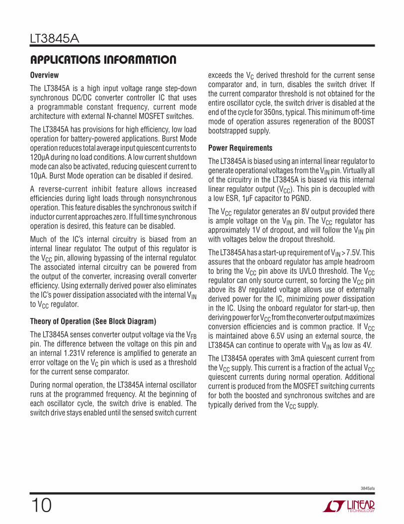
The LT3845A contains a reverse-current inhibit feature to maximize efficiency during light load conditions. This mode of operation allows discontinuous operation and pulse-skipping mode at light loads. Refer to Figure 1.
This feature is enabled with Burst Mode operation, and can also be enabled while Burst Mode operation is disabled by shorting the BURST_EN pin to VFB.
When reverse-current inhibit is enabled, the LT3845A sense amplifier detects inductor currents approaching zero and disables the synchronous switch for the remainder of the switch cycle. If the inductor current is allowed to go negative before the synchronous switch is disabled, the switch node could inductively kick positive with a high dv/dt. The LT3845A prevents this by incorporating a 10mV positive offset at the sense inputs.
With the reverse-current inhibit feature enabled, an LT3845A converter will operate much like a nonsynchronous converter during light loads. Reverse-current inhibit reduces resistive losses associated with inductor ripple currents, which improves operating efficiencies during light-load conditions.
An LT3845A DC/DC converter that is operating in reverse-current inhibit mode has a minimum load requirement of 1mA (BURST_EN = VFB). Since most applications use output-generated power for the LT3845A, this requirement is met by the bias currents of the IC, however, for applications that do not derive power from the output, this requirement is easily accomplished by using a 1.2k resistor connected from VFB to ground as one of the converter output voltage programming resistors (R1). There are no minimum load restrictions when in Burst Mode operation (BURST_EN < 0.5V) or continuous conduction mode (BURST_EN > 2.5V).
Figure 1. Inductor Current vs Mode
PULSE SKIP MODEIL IL
FORCED CONTINUOUS
DECREASINGLOAD
CURRENT
3845A F01

LT3845A
133845afa
Soft-Start
The soft-start function controls the slew rate of the power supply output voltage during start-up. A controlled output voltage ramp minimizes output voltage overshoot, reduces inrush current from the VIN supply, and facilitates supply sequencing. A capacitor, CSS, connected from the CSS pin to SGND, programs the slew rate. The capacitor is charged from an internal 2µA current source producing a ramped voltage. The capacitor voltage overrides the internal reference to the error amplifier. If the VFB pin voltage exceeds the CSS pin voltage then the current threshold set by the DC control voltage, VC, is decreased and the inductor current is lowered. This in turn decreases the output voltage slew rate allowing the CSS pin voltage ramp to catch up to the VFB pin voltage. An internal 100mV offset is added to the VFB pin voltage relative to the CSS pin voltage so that at start-up the soft-start circuit will discharge the VC pin voltage below the DC control voltage equivalent to zero inductor current. This will reduce the input supply inrush current. The soft-start circuit is disabled once the CSS pin voltage has been charged to 200mV above the internal reference of 1.231V.
During a VIN UVLO, VCC UVLO or SHDN UVLO event, the CSS pin voltage is discharged with a 50µA current source. In normal operation the CSS pin voltage is clamped to a diode above the VFB pin voltage. Therefore, the value of the CSS capacitor is relevant to how long of a fault event will retrigger a soft-start. If any of the above UVLO conditions occur, the CSS pin voltage will be discharged with a 50µA current source. There is a diode worth of voltage headroom to ride through the fault before the CSS pin voltage enters its active region and the soft-start function is enabled.
Also, since the CSS pin voltage is clamped to a diode above the VFB pin voltage, during a short circuit the CSS pin voltage is pulled low because the VFB pin voltage is low. Once the short has been removed the VFB pin voltage starts to recover. The soft-start circuit takes control of the output voltage slew rate once the VFB pin voltage has exceeded the slowly ramping CSS pin voltage, reducing the output voltage overshoot during a short circuit recovery.
APPLICATIONS INFORMATIONAdaptive Nonoverlap (NOL) Output Stage
The FET driver output stages implement adaptive nonoverlap control. This feature maintains a constant dead time, preventing shoot-through switch currents, independent of the type, size or operating conditions of the external switch elements.
Each of the two switch drivers contains a NOL control circuit, which monitors the output gate drive signal of the other switch driver. The NOL control circuits interrupt the “turn on” command to their associated switch driver until the other switch gate is fully discharged.
Shutdown
The LT3845A SHDN pin uses a bandgap generated reference threshold of 1.35V. This precision threshold allows use of the SHDN pin for both logic-level controlled applications and analog monitoring applications such as power supply sequencing.
The LT3845A operational status is primarily controlled by a UVLO circuit on the VCC regulator pin. When the IC is enabled via the SHDN pin, only the VCC regulator is enabled. Switching remains disabled until the UVLO threshold is achieved at the VCC pin, when the remainder of the IC is enabled and switching commences.
Because an LT3845A controlled converter is a power transfer device, a voltage that is lower than expected on the input supply could require currents that exceed the sourcing capabilities of that supply, causing the system to lock up in an undervoltage state. Input supply start-up protection can be achieved by enabling the SHDN pin using a resistive divider from the VIN supply to ground. Setting the divider output to 1.35V when that supply is at an adequate voltage prevents an LT3845A converter from drawing large currents until the input supply is able to provide the required power. 120mV of input hysteresis on the SHDN pin allows for almost 10% of input supply droop before disabling the converter.
LT3845A
143845afa
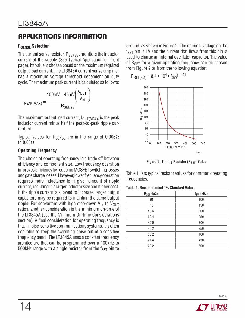
APPLICATIONS INFORMATIONground, as shown in Figure 2. The nominal voltage on the fSET pin is 1V and the current that flows from this pin is used to charge an internal oscillator capacitor. The value of RSET for a given operating frequency can be chosen from Figure 2 or from the following equation:
RSET(kΩ) = 8.4 • 104 • fSW(–1.31)
FREQUENCY (kHz)0
20R S
ET (k
Ω)
40
80
100
120
400
200
3845A F2
60
200100 500300 600
140
160
180
Figure 2. Timing Resistor (RSET) Value
RSENSE Selection
The current sense resistor, RSENSE, monitors the inductor current of the supply (See Typical Application on front page). Its value is chosen based on the maximum required output load current. The LT3845A current sense amplifier has a maximum voltage threshold dependent on duty cycle. The maximum peak current is calculated as follows:
IPEAK(MAX) =
100mV – 45mVVOUTVIN
RSENSE
The maximum output load current, IOUT(MAX), is the peak inductor current minus half the peak-to-peak ripple cur-rent, DI.
Typical values for RSENSE are in the range of 0.005Ω to 0.05Ω.
Operating Frequency
The choice of operating frequency is a trade off between efficiency and component size. Low frequency operation improves efficiency by reducing MOSFET switching losses and gate charge losses. However, lower frequency operation requires more inductance for a given amount of ripple current, resulting in a larger inductor size and higher cost. If the ripple current is allowed to increase, larger output capacitors may be required to maintain the same output ripple. For converters with high step-down VIN to VOUT ratios, another consideration is the minimum on-time of the LT3845A (see the Minimum On-time Considerations section). A final consideration for operating frequency is that in noise-sensitive communications systems, it is often desirable to keep the switching noise out of a sensitive frequency band. The LT3845A uses a constant frequency architecture that can be programmed over a 100kHz to 500kHz range with a single resistor from the fSET pin to
Table 1 lists typical resistor values for common operating frequencies.
Table 1. Recommended 1% Standard Values
RSET (kΩ) fSW (kHz)
191 100
118 150
80.6 200
63.4 250
49.9 300
40.2 350
33.2 400
27.4 450
23.2 500
LT3845A
153845afa
APPLICATIONS INFORMATIONInductor Selection
The critical parameters for selection of an inductor are minimum inductance value, volt-second product, saturation current and/or RMS current.
For a given DIL, The minimum inductance value is calcu-lated as follows:
L ≥ VOUT •
VIN(MAX) – VOUT
fSW • VIN(MAX) • DIL
fSW is the switch frequency.
The typical range of values for DIL is (0.2 • IOUT(MAX)) to (0.5 • IOUT(MAX)), where IOUT(MAX) is the maximum load current of the supply. Using DIL = 0.3 • IOUT(MAX) yields a good design compromise between inductor performance versus inductor size and cost. A value of DIL = 0.3 • IOUT(MAX) produces a ±15% of IOUT(MAX) ripple current around the DC output current of the supply. Lower values of DIL require larger and more costly magnetics. Higher values of DIL will increase the peak currents, requiring more filtering on the input and output of the supply. If DIL is too high, the slope compensation circuit is ineffective and current mode instability may occur at duty cycles greater than 50%. To satisfy slope compensation requirements the minimum inductance is calculated as follows:
LMIN > VOUT •
2DCMAX –1DCMAX
•RSENSE •8.33
fSW
The magnetics vendors specify either the saturation cur-rent, the RMS current or both. When selecting an inductor based on inductor saturation current, use the peak cur-rent through the inductor, IOUT(MAX) + DIL/2. The inductor saturation current specification is the current at which the inductance, measured at zero current, decreases by a specified amount, typically 30%.
When selecting an inductor based on RMS current rating, use the average current through the inductor, IOUT(MAX). The RMS current specification is the RMS current at which the part has a specific temperature rise, typically 40°C, above 25°C ambient.
After calculating the minimum inductance value, the volt-second product, the saturation current and the RMS current for your design, select an off-the-shelf inductor. Contact the Application group at Linear Technology for further support.
For more detailed information on selecting an inductor, please see the “Inductor Selection” section of Linear Technology Application Note 44.
MOSFET Selection
The selection criteria of the external N-channel standard level power MOSFETs include on resistance (RDS(ON)), reverse transfer capacitance (CRSS), maximum drain source voltage (VDSS), total gate charge (QG) and maximum continuous drain current.
For maximum efficiency, minimize RDS(ON) and CRSS. Low RDS(ON) minimizes conduction losses while low CRSS minimizes transition losses. The problem is that RDS(ON) is inversely related to CRSS. In selecting the top MOSFET balancing the transition losses with the conduction losses is a good idea while the bottom MOSFET is dominated by the conduction loss, which is worse during a short-circit condition or at a very low duty cycle.
Calculate the maximum conduction losses of the MOSFETs:
PCOND(TOP) = IOUT(MAX)2 •
VOUTVIN
•RDS(ON)
PCOND(BOT) = IOUT(MAX)2 •
VIN – VOUTVIN
•RDS(ON)
LT3845A
163845afa
APPLICATIONS INFORMATIONNote that RDS(ON) has a large positive temperature dependence. The MOSFET manufacturer’s data sheet contains a curve, RDS(ON) vs Temperature.
In the main MOSFET, transition losses are proportional to VIN
2 and can be considerably large in high voltage applications (VIN > 20V). Calculate the maximum transition losses:
PTRAN(TOP) = k • VIN2 • IOUT(MAX) • CRSS • fSW
where k is a constant inversely related to the gate driver current, approximated by k = 2 for LT3845A applications.
The total maximum power dissipations of the MOSFET are:
PTOP(TOTAL) = PCOND(MAIN) + PTRAN(MAIN)
PBOT(TOTAL) = PCOND(SYNC)
To achieve high supply efficiency, keep the total power dissipation in each switch to less than 3% of the total output power. Also, complete a thermal analysis to ensure that the MOSFET junction temperature is not exceeded.
TJ = TA + P(TOTAL) • qJA
where qJA is the package thermal resistance and TA is the ambient temperature. Keep the calculated TJ below the maximum specified junction temperature, typically 150°C.
Note that when VIN is high and fSW is high, the transition losses may dominate. A MOSFET with higher RDS(ON) and lower CRSS may provide higher efficiency. MOSFETs with higher voltage VDSS specification usually have higher RDS(ON) and lower CRSS.
Choose the MOSFET VDSS specification to exceed the maximum voltage across the drain to the source of the MOSFET, which is VIN(MAX) plus any additional ringing on the switch node. Ringing on the switch node can be greatly reduced with good PCB layout and, if necessary, an RC snubber.
In some applications, parasitic FET capacitances couple the negative going switch node transient onto the bottom gate drive pin of the LT3845A, causing a negative voltage
in excess of the Absolute Maximum Rating to be imposed on that pin. Connection of a catch Schottky diode from this pin to ground will eliminate this effect. A 1A current rating is typically sufficient of the diode.
The internal VCC regulator is capable of sourcing up to 40mA limiting the maximum total MOSFET gate charge, QG, to 35mA/fSW. The QG vs VGS specification is typically provided in the MOSFET data sheet. Use QG at VGS of 8V. If VCC is back driven from an external supply, the MOSFET drive current is not sourced from the internal regulator of the LT3845A and the QG of the MOSFET is not limited by the IC. However, note that the MOSFET drive current is supplied by the internal regulator when the external supply back driving VCC is not available such as during start-up or short circuit.
The manufacturer’s maximum continuous drain current specification should exceed the peak switch current, IOUT(MAX) + DIL/2.
During the supply start-up, the gate drive levels are set by the VCC voltage regulator, which is approximately 8V. Once the supply is up and running, the VCC can be back driven by an auxiliary supply such as VOUT. It is important not to exceed the manufacturer’s maximum VGS specification. A standard level threshold MOSFET typically has a VGS maximum of 20V.
Input Capacitor Selection
A local input bypass capacitor is required for buck converters because the input current is pulsed with fast rise and fall times. The input capacitor selection criteria are based on the bulk capacitance and RMS current capability. The bulk capacitance will determine the supply input ripple voltage. The RMS current capability is used to prevent overheating the capacitor.
The bulk capacitance is calculated based on maximum input ripple, DVIN:
CIN(BULK) =
IOUT(MAX) • VOUT
DVIN • fSW • VIN(MIN)
LT3845A
173845afa
DVIN is typically chosen at a level acceptable to the user. 100mV to 200mV is a good starting point. Aluminum elec-trolytic capacitors are a good choice for high voltage, bulk capacitance due to their high capacitance per unit area.
The capacitor’s RMS current is:
ICIN(RMS) = IOUTVOUT(VIN – VOUT)
(VIN)2
If applicable, calculate it at the worst case condition, VIN = 2VOUT. The RMS current rating of the capacitor is specified by the manufacturer and should exceed the calculated ICIN(RMS). Due to their low ESR (Equivalent Series Resistance), ceramic capacitors are a good choice for high voltage, high RMS current handling. Note that the ripple current ratings from aluminum electrolytic capacitor manufacturers are based on 2000 hours of life. This makes it advisable to further derate the capacitor or to choose a capacitor rated at a higher temperature than required.
The combination of aluminum electrolytic capacitors and ceramic capacitors is an economical approach to meeting the input capacitor requirements. The capacitor voltage rating must be rated greater than VIN(MAX). Multiple capacitors may also be paralleled to meet size or height requirements in the design. Locate the capacitor very close to the MOSFET switch and use short, wide PCB traces to minimize parasitic inductance.
Output Capacitor Selection
The output capacitance, COUT, selection is based on the design’s output voltage ripple, DVOUT and transient load requirements. DVOUT is a function of DIL and the COUT ESR. It is calculated by:
DVOUT = DIL • ESR + 1
(8 • fSW •COUT )
APPLICATIONS INFORMATIONThe maximum ESR required to meet a DVOUT design requirement can be calculated by:
ESR(MAX)= (DVOUT )(L)(fSW)
VOUT • 1–VOUT
VIN(MAX)
Worst-case DVOUT occurs at highest input voltage. Use paralleled multiple capacitors to meet the ESR requirements. Increasing the inductance is an option to lower the ESR require-ments. For extremely low DVOUT, an additional LC filter stage can be added to the output of the supply. Application Note 44 has some good tips on sizing an additional output filter.
Output Voltage Programming
A resistive divider sets the DC output voltage according to the following formula:
R2 = R1
VOUT1.231V
–1
The external resistor divider is connected to the output of the converter as shown in Figure 3. Tolerance of the feedback resistors will add additional error to the output voltage.
Example: VOUT = 12V; R1 = 10k
R2 = 10k 12V
1.231V− 1
= 87.48kΩ −use 86.6k 1%
The VFB pin input bias current is typically 25nA, so use of extremely high value feedback resistors could cause a converter output that is slightly higher than expected. Bias current error at the output can be estimated as:
DVOUT(BIAS) = 25nA • R2
LT3845A
183845afa
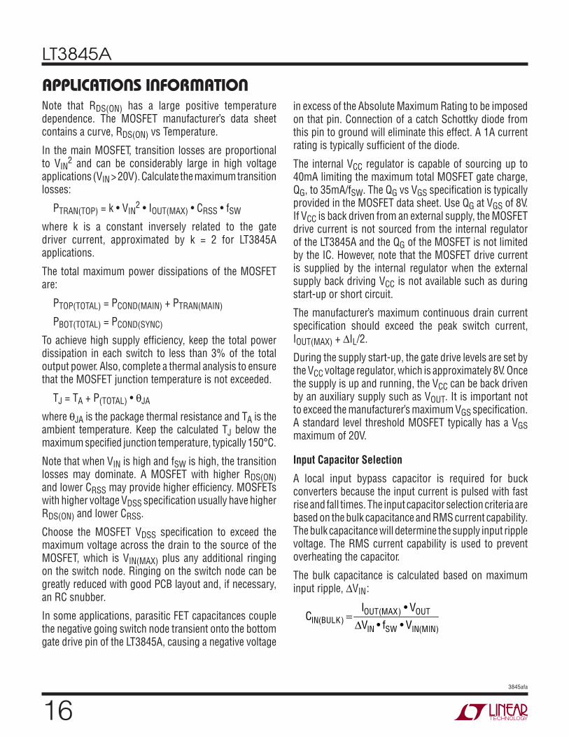
Supply UVLO and Shutdown
The SHDN pin has a precision voltage threshold with hysteresis which can be used as an undervoltage lockout threshold (UVLO) for the power supply. Undervoltage lockout keeps the LT3845A in shutdown until the supply input voltage is above a certain voltage programmed by the user. The hysteresis voltage prevents noise from falsely tripping UVLO.
Resistors are chosen by first selecting RB. Then
RA =RB •
VSUPPLY(ON)
1.35V–1
VSUPPLY(ON) is the input voltage at which the undervoltage lockout is disabled and the supply turns on.
Example: Select RB = 49.9k, VSUPPLY(ON) = 14.5V (based on a 15V minimum input voltage)
RA = 49.9k • 14.5V1.35V
– 1
= 486.1k (499k resistor is selected)
If low supply current in standby mode is required, select a higher value of RB.
The supply turn off voltage is 9% below turn on. In the example the VSUPPLY(OFF) would be 13.2V.
If additional hysteresis is desired for the enable function, an external positive feedback resistor can be used from the LT3845A regulator output.
The shutdown function can be disabled by connecting the SHDN pin to the VIN through a large value pull-up resistor. This pin contains a low impedance clamp at 6V, so the SHDN pin will sink current from the pull-up resistor(RPU):
ISHDN
=VIN – 6V
RPU
Because this arrangement will clamp the SHDN pin to the 6V, it will violate the 5V absolute maximum voltage rating of the pin. This is permitted, however, as long as the absolute maximum input current rating of 1mA is not exceeded. Input SHDN pin currents of <100µA are recommended: a 1MΩ or greater pull-up resistor is typically used for this configuration.
Soft-Start
The desired soft-start time (tSS) is programmed via the CSS capacitor as follows:
CSS =
2µA • tSS1.231V
The amount of time in which the power supply can withstand a VIN, VCC or VSHDN UVLO fault condition (tFAULT) before the CSS pin voltage enters its active region is approximated by the following formula:
tFAULT =
CSS •0.65V50µA
APPLICATIONS INFORMATIONL1
VFB PIN
R2
R1
VOUT
COUT
3845A F03
SHDN PIN
RA
RB
VSUPPLY
3845A F04
Figure 3. Output Voltage Feedback Divider
Figure 4. Undervoltage Feedback Divider
LT3845A
193845afa
Oscillator SYNC
The oscillator can be synchronized to an external clock. Set the RSET resistor at least 10% below the desired sync frequency.
It is recommended that the SYNC pin be driven with a square wave that has amplitude greater than 2V, pulse width greater than 1µs and rise time less than 500ns. The rising edge of the sync wave form triggers the discharge of the internal oscillator capacitor. The SYNC pin is not available in the N-Package.
Minimum On-Time Considerations (Buck Mode)
Minimum on-time tON(MIN) is the smallest amount of time that the LT3845A is capable of turning the top MOSFET on and off again. It is determined by internal timing delays and the amount of gate charge required turning on the top MOSFET. Low duty cycle applications may approach this minimum on-time limit and care should be taken to ensure that:
tON =
VOUTVIN • fSW
> tON(MIN)
where tON(MIN) is 400ns worst case.
If the duty cycle falls below what can be accommodated by the minimum on-time, the LT3845A will begin to skip cycles. The output will be regulated, but the ripple current and ripple voltage will increase. If lower frequency operation is acceptable, the on-time can be increased above tON(MIN) for the same step-down ratio.
Layout Considerations
The LT3845A is typically used in DC/DC converter designs that involve substantial switching transients. The switch drivers on the IC are designed to drive large capacitances and, as such, generate significant transient currents themselves. Careful consideration must be made regarding supply bypass capacitor locations to avoid corrupting the ground reference used by IC.
Typically, high current paths and transients from the input supply and any local drive supplies must be kept
isolated from SGND, to which sensitive circuits such as the error amp reference and the current sense circuits are referred.
Effective grounding can be achieved by considering switch current in the ground plane, and the return current paths of each respective bypass capacitor. The VIN bypass return, VCC bypass return, and the source of the synchronous FET carry PGND currents. SGND originates at the negative terminal of the VOUT bypass capacitor, and is the small signal reference for the LT3845A.
Don’t be tempted to run small traces to separate ground paths. A good ground plane is important as always, but PGND referred bypass elements must be oriented such that transient currents in these return paths do not corrupt the SGND reference.
During the dead-time between switch conduction, the body diode of the synchronous FET conducts inductor current. Commutating this diode requires a significant charge contribution from the main switch. At the instant the body diode commutates, a current discontinuity is created and parasitic inductance causes the switch node to fly up in response to this discontinuity. High currents and excessive parasitic inductance can generate extremely fast dV/dt rise times. This phenomenon can cause avalanche breakdown in the synchronous FET body diode, significant inductive overshoot on the switch node, and shoot-through currents via parasitic turn-on of the synchronous FET. Layout practices and component orientations that minimize parasitic inductance on this node is critical for reducing these effects.
Ringing waveforms in a converter circuit can lead to device failure, excessive EMI, or instability. In many cases, you can damp a ringing waveform with a series RC network across the offending device. In LT3845A applications, any ringing will typically occur on the switch node, which can usually be reduced by placing a snubber across the synchronous FET. Use of a snubber network, however, should be considered a last resort. Effective layout practices typically reduce ringing and overshoot, and will eliminate the need for such solutions.
APPLICATIONS INFORMATION
LT3845A
203845afa
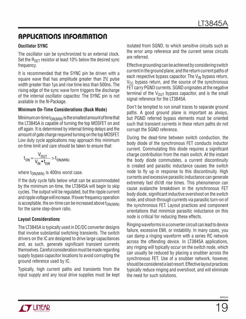
APPLICATIONS INFORMATIONEffective grounding techniques are critical for successful DC/DC converter layouts. Orient power path components such that current paths in the ground plane do not cross through signal ground areas. Signal ground refers to the Exposed Pad on the backside of the LT3845A IC in the TSSOP package. SGND is referenced to the (–) terminal of the VOUT decoupling capacitor and is used as the converter voltage feedback reference. Power ground currents are controlled on the LT3845A via the PGND pin, and this ground references the high current synchronous switch drive components, as well as the local VCC supply. It is important to keep PGND and SGND voltages consistent with each other, so separating these grounds with thin traces is not recommended. When the synchronous FET is turned on, gate drive surge currents return to the LT3845A PGND pin from the FET source. The BOOST supply refresh surge currents also return through this same path. The synchronous FET must be oriented such that these PGND return currents do not corrupt the SGND reference. Problems caused by the PGND return path are generally recognized during heavy load conditions, and are typically evidenced as multiple switch pulses occurring during a single switch cycle. This behavior indicates that SGND is being corrupted and grounding should be improved. SGND corruption can often be eliminated, however, by adding a small capacitor (100pF to 200pF) across the synchronous switch FET from drain to source.
The high di/dt loop formed by the switch MOSFETs and the input capacitor (CIN) should have short wide traces to minimize high frequency noise and voltage stress from inductive ringing. Surface mount components are preferred to reduce parasitic inductances from component leads. Connect the drain of the main switch MOSFET directly to the (+) plate of CIN, and connect the source of the syn-chronous switch MOSFET directly to the (–) terminal of CIN. This capacitor provides the AC current to the switch MOSFETs. Switch path currents can be controlled by orienting switch FETs, the switched inductor, and input and output decoupling capacitors in close proximity to each other.
Locate the VCC and BOOST decoupling capacitors in close proximity to the IC. These capacitors carry the MOSFET drivers’ high peak currents. Locate the small-signal components away from high frequency switching nodes (BOOST, SW, TG, VCC and BG). Small-signal nodes are oriented on the left side of the LT3845A, while high current switching nodes are oriented on the right side of the IC to simplify layout. This also helps prevent corruption of the SGND reference.
Connect the VFB pin directly to the feedback resistors independent of any other nodes, such as the SENSE– pin. The feedback resistors should be connected between the (+) and (–) terminals of the output capacitor (COUT). Locate the feedback resistors in close proximity to the LT3845A to minimize the length of the high impedance VFB node.
The SENSE– and SENSE+ traces should be routed together and kept as short as possible.
The LT3845A TSSOP package has been designed to efficiently remove heat from the IC via the Exposed Pad on the backside of the package. The Exposed Pad is soldered to a copper footprint on the PCB. This footprint should be made as large as possible to reduce the thermal resistance of the IC case to ambient air. See Figure 5 for placement of power path components.
Figure 5. Orientation of Components Isolates Power Path and PGND Currents, Preventing Corruption of SGND Reference
BOOST
VCC
SW
PGNDSGND
LT3845ASGNDREFERRED
COMPONENTS
+
+ BG
TG
VOUT
3845A AI03
VIN
ISENSE
SW
LT3845A
213845afa
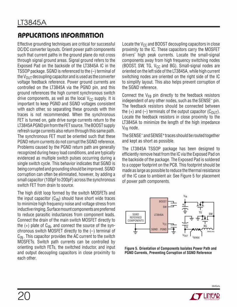
TYPICAL APPLICATIONS9V-16V to 3.3V at 10A DC/DC Converter Capable of Withstanding 60V Transients,
All Ceramic Capacitors and Soft-Start Enabled
VIN
SHDN
CSS
BURST_EN
VFB
VC
SYNC
fSET
BOOST
TG
SW
VCC
BG
PGND
SENSE+
SENSE–
SGND
D2A BAV99
C51µF16V
C38200pF
M1Si7370DP
M2Si7370DP
D1
L13.3µH
RSENSE0.006ΩLT3845A
C42.2µF16V
3845A TA02
C26800pF
COUT100µF6.3V×5
VOUT3.3V10A
R31.1M
VIN9V TO 16V
60V TRANSIENTS CIN20.1µF100V
R649.9k
VIN
R5100k
SYNC
R74.99k
D312V
R425k
R110k
R216.9k
CIN2.2µF100V×4
CIN: TDK C4532X7R2A225KCOUT: MURATA GRM32ER60J107ME20D1: DIODES INC. B3100L1: WURTH 7443551370
D2BBAV99
Q160V
LOAD CURRENT (A)0.1
65
EFFI
CIEN
CY(%
)POW
ER LOSS (W)
70
75
80
85
95
1 10
3845A TA02b
90
0
1
2
3
4
6
5VIN = 9V
VIN = 14VVIN = 16V
POWER LOSSVIN = 14V
Efficiency and Power Loss
LT3845A
223845afa
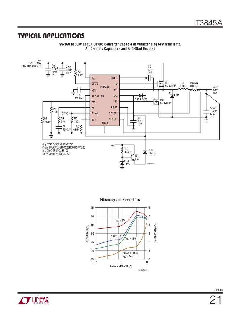
TYPICAL APPLICATIONS9V-16V to 5V at 10A DC/DC Converter, 500kHz Frequency Operation,
Capable of Withstanding 36V Transients, All Ceramic Capacitors, Soft-Start and Burst Mode Enabled
VIN
SHDN
CSS
BURST_EN
VFB
VC
SYNC
fSET
BOOST
TG
SW
VCC
BG
PGND
SENSE+
SENSE–
SGND
D2 BAS19
C51µF16V
C38200pF M1
Si7884DP
M2Si7884DP
Si1555DL
D1
L12.7µH
RSENSE0.005ΩLT3845A
C42.2µF16V
C61µF
D3BBAV99
D3ABAV99
3845A TA03
C25600pF
C1100pF
COUT100µF6.3V×4
VOUT5V10A
R31.1M
VIN9V TO 16V
36V TRANSIENTS CIN20.1µF50V
R623.2k
R410k
R149.9k
R2154k
CIN6.8µF50V×4
CIN: TDK C4532X7R1H685KCOUT: MURATA GRM32ER60J107ME20D1: DIODES INC. B170L1: WURTH 744318270LF
Efficiency and Power Loss
LOAD CURRENT (A)0.1
70
EFFI
CIEN
CY (%
)POW
ER LOSS (W)
75
80
85
90
100
1 10
3845A TA03b
95
0
1
2
3
4
6
5
VIN = 9V
VIN = 14V
VIN = 16V
POWER LOSSVIN = 14V
LT3845A
233845afa
TYPICAL APPLICATIONS9V-24V to 3.3V, 2-Phase at 10A per Phase, DC/DC Converter with Spread Spectrum Operation
VIN
SHDN
CSS
BURST_EN
VFB
VC
SYNC
fSET
BOOST
TG
SW
VCC
BG
PGND
SENSE+
SENSE–
SGND
C51µF16V
D2 BAS19
C3 8200pF
C1147pF
M1Si7850DP
M2Si7850DP
D1B160
L14.7µH
RSENSE0.005ΩLT3845A
C42.2µF16V
R31.21M
R41.21M
VIN24V
R6130k
SYNC
CIN6.8µF50V×2
CIN: TDK C4532X7R1H685KCOUT: MURATA GRM32ER60J107ME20D1, D3: DIODES, INC. B160L1, L2: VISHAY IHLP-5050FD-01
VIN
SHDN
CSS
BURST_EN
VFB
VC
SYNC
fSET
BOOST
TG
SW
VCC
BG
PGND
SENSE+
SENSE–
SGND
C101µF16V
C8 8200pF
M3Si7850DP
M4Si7850DP
D3B160
L24.7µH
RSENSE20.005ΩLT3845A
C92.2µF16V
3845A TA05
R10130k
R94.99k
C75600pF
C647pF
CIN30.1µF100V
SYNC1
SYNC2
SYNC
R110k
R11500k
R1225k
D55.7V
C110.1µF
Q1
R216.8k
LTC6908-1V+
GND
SET3
6
5
4
1
2
3
OUT1
OUT2
MOD
COUT100µF6.3V×6
VOUT3.3V20A
D4 BAS19
LT3845A
243845afa
FE Package16-Lead Plastic TSSOP (4.4mm)(Reference LTC DWG # 05-08-1663)
Exposed Pad Variation BC
FE16 (BC) TSSOP 0204
0.09 – 0.20(.0035 – .0079)
0° – 8°
0.25REF
0.50 – 0.75(.020 – .030)
4.30 – 4.50*(.169 – .177)
1 3 4 5 6 7 8
10 9
4.90 – 5.10*(.193 – .201)
16 1514 13 12 11
1.10(.0433)
MAX
0.05 – 0.15(.002 – .006)
0.65(.0256)
BSC
2.94(.116)
0.195 – 0.30(.0077 – .0118)
TYP
2RECOMMENDED SOLDER PAD LAYOUT
0.45 ± 0.05
0.65 BSC
4.50 ± 0.10
6.60 ± 0.10
1.05 ± 0.10
2.94(.116)
3.58(.141)
3.58(.141)
MILLIMETERS(INCHES) *DIMENSIONS DO NOT INCLUDE MOLD FLASH. MOLD FLASH
SHALL NOT EXCEED 0.150mm (.006") PER SIDE
NOTE:1. CONTROLLING DIMENSION: MILLIMETERS
2. DIMENSIONS ARE IN
3. DRAWING NOT TO SCALE
SEE NOTE 4
4. RECOMMENDED MINIMUM PCB METAL SIZE FOR EXPOSED PAD ATTACHMENT
6.40(.252)BSC
PACKAGE DESCRIPTION

LT3845A
253845afa
Information furnished by Linear Technology Corporation is believed to be accurate and reliable. However, no responsibility is assumed for its use. Linear Technology Corporation makes no representation that the interconnection of its circuits as described herein will not infringe on existing patent rights.
REVISION HISTORYREV DATE DESCRIPTION PAGE NUMBER
A 11/10 Added Military grade to Absolute Maximum Ratings and Order Information.Added Military grade to Note 3 in the Electrical Characteristics
24
LT3845A
263845afa
Linear Technology Corporation1630 McCarthy Blvd., Milpitas, CA 95035-7417 (408) 432-1900 FAX: (408) 434-0507 www.linear.com ” LINEAR TECHNOLOGY CORPORATION 2010
LT 1110 • PRINTED IN USA
RELATED PARTS
TYPICAL APPLICATION
PART NUMBER DESCRIPTION COMMENTS
LT3800 60V, Low IQ, Single Output Synchronous Step-Down DC/DC Controller
Fixed 200kHz Operating Frequency 4V≤ VIN ≤ 60V, 1.23V ≤ VOUT ≤ 36V, IQ = 120µA, TSSOP-16
LTC3844 60V, Low IQ, Single Output Step-Down DC/DC Controller Synchronizable Fixed Frequency 50kHz to 600kHz, 4V ≤ VIN ≤ 60V, 1.23V ≤ VOUT ≤ 36V, IQ = 120µA, TSSOP-16
LT3724 60V, Low IQ, DC/DC Controller Multi Topology Fixed 200kHz Operating Frequency 4V ≤ VIN ≤ 60V, 1.23 ≤ VOUT ≤ 36V, IQ = 100µA, TSSOP-16
LT3741 High Power, Constant Current, Constant Voltage, Synchronous, Step Down Controller
Adjustable Fixed Frequency 200kHz to 1MHz 6V ≤ VIN ≤ 36V, VOUT Up to (VIN –2)
LTC3824 60V, Low IQ, Step-Down DC/DC Controller, 100% Duty Cycle
Selectable Fixed Frequency 200kHz to 600kHz 4V≤ VIN ≤ 60V, 0.8V ≤ VOUT ≤ VIN, IQ = 40µA, MSOP-10E
LTC3834/LTC3834-1 LTC3835/LTC3835-1
Low IQ, Single Output Synchronous Step-Down DC/DC Controller with 99% Duty Cycle
Phase-Lockable Fixed Frequency 140kHz to 650kHz, 4V≤ VIN ≤ 36V, 0.8V ≤ VOUT ≤ 10V, IQ = 30µA/80µA
LTC3890 60V, Low IQ, Dual 2-Phase Synchronous Step-Down DC/DC Controller
Phase-Lockable Fixed Frequency 50kHz to 900kHz 4V ≤ VIN ≤ 60V, 0.8V ≤ VOUT ≤ 24V, IQ = 50µA
LTC3857/LTC3857-1 LTC3858/LTC3858-1
Low IQ, Dual Output 2-Phase Synchronous Step-Down DC/DC Controllers with 99% Duty Cycle
Phase-Lockable Fixed Frequency 50kHz to 900kHz, 4V≤ VIN ≤ 38V, 0.8V ≤ VOUT ≤ 24V, IQ = 50µA/170µA
LTC3859 Low IQ, Triple Output Buck/Buck/Boost Synchronous DC/DC Controller
All Outputs Remain in Regulation Through Cold Crank 2.5V≤ VIN ≤ 38V, VOUT(BUCKS) Up to 24V, VOUT(BOOST) Up to 60V, IQ = 55µA
9V-16V to 3.3V at 5A DC/DC Converter, Frequency Synchronization Range 150kHz to 300kHz, Capable of Withstanding 60V Transients, All Ceramic Capacitors, Soft-Start and Burst Mode Enabled
VIN
SHDN
CSS
BURST_EN
VFB
VC
SYNC
fSET
BOOST
TG
SW
VCC
BG
PGND
SENSE+
SENSE–
SGND
D2 BAS521
C51µF16V
C38200pF M1
Si7850DP
M2Si7850DP
D1B160
L110µH
RSENSE0.01ΩLT3845A
C42.2µF16V
3845A TA04
C25600pF
C1100pF
COUT100µF6.3V×4
VOUT3.3V5A
R31.1M
VIN9V TO 16V
60V TRANSIENTS CIN20.1µF100V
R6130k
SYNC
R410k
R5100k
R110k
R216.8k
CIN2.2µF100V×4
CIN: TDK C4532X7R2A225KCOUT: MURATA GRM32ER60J107ME20L1: VISHAY IHLP-5050FD-01M1, M2: VISHAY Si7850DP


