15V to 60V, Three-Phase Brushless DC Motor Pre-Driver The ...

LT3763
13763fa
For more information www.linear.com/LT3763
PWM Dimming
PWM10V/DIV
VSW50V/DIV
IL5A/DIV
5µs/DIV 3763 TA01b
Typical applicaTion
FeaTures DescripTion
60V High Current Step-Down LED Driver Controller
The LT®3763 is a fixed frequency, synchronous, step-down DC/DC controller designed to accurately regulate output currents up to 20A. The average current mode control-ler will maintain inductor current regulation over a wide output voltage range from 0V to 55V. Output current is set by analog voltages on the CTRL pins and an external sense resistor. Voltage regulation and overvoltage protec-tion are set with a voltage divider from the output to the FB pin. The switching frequency is programmable from 200kHz to 1MHz through an external resistor on the RT pin or with the SYNC pin and an external clock signal. Input and output current sensing provides input current limiting and an accurate measurement of these currents. The FBIN pin is provided for applications requiring a peak power tracking function.
Additional features include an accurate external reference voltage for use with the CTRL pins, an accurate UVLO/EN pin that allows for programmable UVLO hysteresis, a PWM driver for LED applications, output voltage fault detection, and thermal shutdown.
20A, Pulse Width Modulated, Single LED Driver
applicaTions
n Accurately Control Input and Output Currentn 3000:1 True Color PWM™ Dimmingn ±1.5% Voltage Regulation Accuracyn ±6% Current Regulation Accuracyn 6V to 60V Input Voltage Rangen Wide Output Range Up to 55Vn <2µA Shutdown Currentn Control Pin for Thermal Control of Load Currentn Input and Output Current Monitor and Limitn Open, Short, and C/10 Fault Detectionn PWM Driver Output for LED Applicationsn Thermally Enhanced 28-Lead FE Package
n High Power Architectural Lightingn Automotive Lightingn Aviation and Marine Strobe Lightsn Solar-Powered Chargers, Laser Diodes
100µF
VIN10V TO 30V
2.5mΩ
1k 1k
82.5k
EN/UVLO
FBIN
TG
VIN
BOOST
VREF
CTRL1
CTRL2LT3763
SW
BG
GND
VC
SENSE+
SENSE–
INTVCC
220nF
1.5µH
22µF
2.5mΩ
FB
FAULT
59k
4.7nF
47.5k
3763 TA01
12.1k
2.2µF
470k
PWMOUT
VOUT6V, 20A MAXIMUM
220µF×2
PWMSYNC
SS
10nF
RT
45.3k
84.5k
15.4k
33nF
10Ω 10Ω47.5kΩ
1µF
50k
4.7µF
IVINNIVINP
IVINMON
ISMON1nF
1nF
50Ω
50Ω
L, LT, LTC, LTM, Linear Technology and the Linear logo are registered trademarks and True Color PWM is a trademark of Linear Technology Corporation. All other trademarks are the property of their respective owners. Protected by U.S. Patents including 7199560, 7321203 and others pending.
LT3763
23763fa
For more information www.linear.com/LT3763
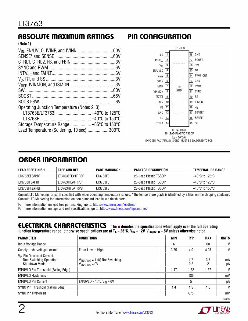
pin conFiguraTionabsoluTe MaxiMuM raTings
VIN, EN/UVLO, IVINP, and IVINN ...............................60VSENSE+ and SENSE– .................................................60VCTRL1, CTRL2, FB, and FBIN ......................................3VSYNC and PWM ..........................................................6VINTVCC and FAULT.......................................................6VVC, RT, and SS ............................................................3VVREF, IVINMON, and ISMON ........................................3VSW ............................................................................60VBOOST ......................................................................66VBOOST-SW ..................................................................6VOperating Junction Temperature (Notes 2, 3)
LT3763E/LT3763I .............................. –40°C to 125°C LT3763H ............................................ –40°C to 150°C
Storage Temperature Range .................. –65°C to 150°CLead Temperature (Soldering, 10 sec) ................... 300°C
(Note 1)
1
2
3
4
5
6
7
8
9
10
11
12
13
14
TOP VIEW
FE PACKAGE28-LEAD PLASTIC TSSOP
28
27
26
25
24
23
22
21
20
19
18
17
16
15
BG
INTVCC
VIN
EN/UVLO
VREF
IVINN
IVINP
IVINMON
FAULT
FBIN
FB
GND
CTRL2
CTRL1
GND
BOOST
SW
TG
PWM_OUT
GND
PWM
SYNC
RT
ISMON
VC
SENSE+
SENSE–
SS
29GND
θJA = 30°C/W
EXPOSED PAD (PIN 29) IS GND, MUST BE SOLDERED TO PCB
orDer inForMaTionLEAD FREE FINISH TAPE AND REEL PART MARKING* PACKAGE DESCRIPTION TEMPERATURE RANGE
LT3763EFE#PBF LT3763EFE#TRPBF LT3763FE 28-Lead Plastic TSSOP –40°C to 125°C
LT3763IFE#PBF LT3763IFE#TRPBF LT3763FE 28-Lead Plastic TSSOP –40°C to 125°C
LT3763HFE#PBF LT3763HFE#TRPBF LT3763FE 28-Lead Plastic TSSOP –40°C to 150°C
Consult LTC Marketing for parts specified with wider operating temperature ranges. *The temperature grade is identified by a label on the shipping container. Consult LTC Marketing for information on non-standard lead based finish parts.For more information on lead free part marking, go to: http://www.linear.com/leadfree/ For more information on tape and reel specifications, go to: http://www.linear.com/tapeandreel/
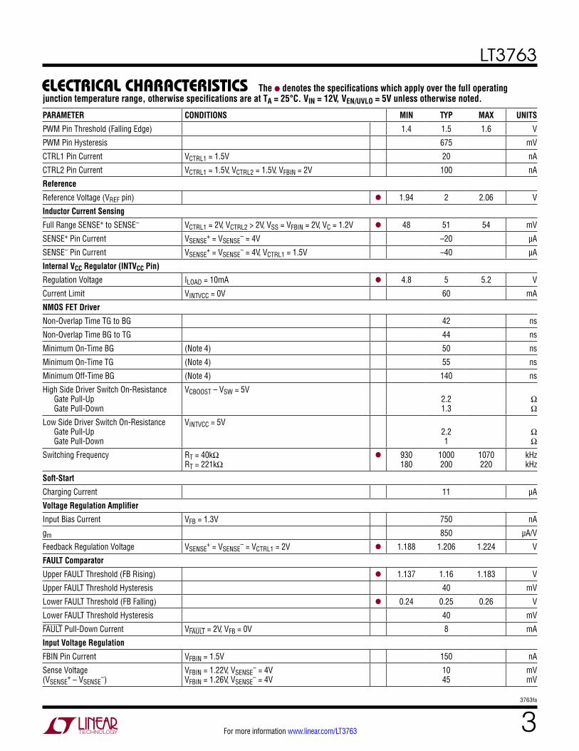
elecTrical characTerisTics The l denotes the specifications which apply over the full operating junction temperature range, otherwise specifications are at TA = 25°C. VIN = 12V, VEN/UVLO = 5V unless otherwise noted.
PARAMETER CONDITIONS MIN TYP MAX UNITS
Input Voltage Range 6 60 V
Supply Undervoltage Lockout From Low to High 3.75 4.0 4.25 V
VIN Pin Quiescent Current Non-Switching Operation Shutdown Mode
VEN/UVLO = 1.4V, Not Switching VEN/UVLO = 0V
1.7 0.2
3.5 2
mA µA
EN/UVLO Pin Threshold (Falling Edge) 1.47 1.52 1.57 V
EN/UVLO Hysteresis 185 mV
EN/UVLO Pin Current EN/UVLO = 1.4V, VIN = 6V 5 µA
SYNC Pin Threshold (Falling Edge) 1.4 1.5 1.6 V
SYNC Pin Hysteresis 675 mV
LT3763
33763fa
For more information www.linear.com/LT3763
elecTrical characTerisTics The l denotes the specifications which apply over the full operating junction temperature range, otherwise specifications are at TA = 25°C. VIN = 12V, VEN/UVLO = 5V unless otherwise noted.
PARAMETER CONDITIONS MIN TYP MAX UNITS
PWM Pin Threshold (Falling Edge) 1.4 1.5 1.6 V
PWM Pin Hysteresis 675 mV
CTRL1 Pin Current VCTRL1 = 1.5V 20 nA
CTRL2 Pin Current VCTRL1 = 1.5V, VCTRL2 = 1.5V, VFBIN = 2V 100 nA
Reference
Reference Voltage (VREF pin) l 1.94 2 2.06 V
Inductor Current Sensing
Full Range SENSE+ to SENSE– VCTRL1 = 2V, VCTRL2 > 2V, VSS = VFBIN = 2V, VC = 1.2V l 48 51 54 mV
SENSE+ Pin Current VSENSE+ = VSENSE
– = 4V –20 µA
SENSE– Pin Current VSENSE+ = VSENSE
– = 4V, VCTRL1 = 1.5V –40 µA
Internal VCC Regulator (INTVCC Pin)
Regulation Voltage ILOAD = 10mA l 4.8 5 5.2 V
Current Limit VINTVCC = 0V 60 mA
NMOS FET Driver
Non-Overlap Time TG to BG 42 ns
Non-Overlap Time BG to TG 44 ns
Minimum On-Time BG (Note 4) 50 ns
Minimum On-Time TG (Note 4) 55 ns
Minimum Off-Time BG (Note 4) 140 ns
High Side Driver Switch On-Resistance Gate Pull-Up Gate Pull-Down
VCBOOST – VSW = 5V 2.2 1.3
Ω Ω
Low Side Driver Switch On-Resistance Gate Pull-Up Gate Pull-Down
VINTVCC = 5V 2.2 1
Ω Ω
Switching Frequency RT = 40kΩ RT = 221kΩ
l 930 180
1000 200
1070 220
kHz kHz
Soft-Start
Charging Current 11 µA
Voltage Regulation Amplifier
Input Bias Current VFB = 1.3V 750 nA
gm 850 µA/V
Feedback Regulation Voltage VSENSE+ = VSENSE
– = VCTRL1 = 2V l 1.188 1.206 1.224 V
FAULT Comparator
Upper FAULT Threshold (FB Rising) l 1.137 1.16 1.183 V
Upper FAULT Threshold Hysteresis 40 mV
Lower FAULT Threshold (FB Falling) l 0.24 0.25 0.26 V
Lower FAULT Threshold Hysteresis 40 mV
FAULT Pull-Down Current VFAULT = 2V, VFB = 0V 8 mA
Input Voltage Regulation
FBIN Pin Current VFBIN = 1.5V 150 nA
Sense Voltage (VSENSE
+ – VSENSE–)
VFBIN = 1.22V, VSENSE– = 4V
VFBIN = 1.26V, VSENSE– = 4V
10 45
mV mV
LT3763
43763fa
For more information www.linear.com/LT3763
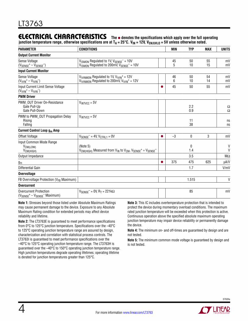
elecTrical characTerisTics
Note 1: Stresses beyond those listed under Absolute Maximum Ratings may cause permanent damage to the device. Exposure to any Absolute Maximum Rating condition for extended periods may affect device reliability and lifetime.Note 2: The LT3763E is guaranteed to meet performance specifications from 0°C to 125°C junction temperature. Specifications over the –40°C to 125°C operating junction temperature range are assured by design, characterization and correlation with statistical process controls. The LT3763I is guaranteed to meet performance specifications over the –40°C to 125°C operating junction temperature range. The LT3763H is guaranteed over the –40°C to 150°C operating junction temperature range. High junction temperatures degrade operating lifetimes; operating lifetime is derated for junction temperatures greater than 125°C.
PARAMETER CONDITIONS MIN TYP MAX UNITS
Output Current Monitor
Sense Voltage (VSENSE
+ – VSENSE–)
VISMON Regulated to 1V, VSENSE– = 10V
VISMON Regulated to 200mV, VSENSE– = 10V
45 5
50 10
55 15
mV mV
Input Current Monitor
Sense Voltage (VIVIN
+ – VIVIN–)
VIVINMON Regulated to 1V, VIVIN+ = 12V
VIVINMON Regulated to 200mV, VIVIN+ = 12V
46 6
50 10
54 14
mV mV
Input Current Limit Sense Voltage (VIVIN
+ – VIVIN–)
l 45 50 55 mV
PWM Driver
PWM_OUT Driver On-Resistance Gate Pull-Up Gate Pull-Down
VINTVCC = 5V 2.2 0.9
Ω Ω
PWM to PWM_OUT Propagation Delay Rising Falling
VINTVCC = 5V 11 38
ns ns
Current Control Loop gm Amp
Offset Voltage VSENSE– = 4V, VCTRL1 = 0V l –3 0 3 mV
Input Common Mode Range VCM(LOW) VCM(HIGH)
(Note 5) VCM(HIGH) Measured from VIN to VCM, VSENSE
+ = VSENSE–
0
1.4
V V
Output Impedance 3.5 MΩ
gm l 375 475 625 µA/V
Differential Gain 1.7 V/mV
Overvoltage
FB Overvoltage Protection (VFB Maximum) 1.515 V
Overcurrent
Overcurrent Protection (VSENSE
+ – VSENSE– Maximum)
VSENSE– = 0V, RT = 221kΩ 85 mV
The l denotes the specifications which apply over the full operating junction temperature range, otherwise specifications are at TA = 25°C. VIN = 12V, VEN/UVLO = 5V unless otherwise noted.
Note 3: This IC includes overtemperature protection that is intended to protect the device during momentary overload conditions. The maximum rated junction temperature will be exceeded when this protection is active. Continuous operation above the specified absolute maximum operating junction temperature may impair device reliability or permanently damage the device.Note 4: The minimum on- and off-times are guaranteed by design and are not tested.Note 5: The minimum common mode voltage is guaranteed by design and is not tested.
LT3763
53763fa
For more information www.linear.com/LT3763
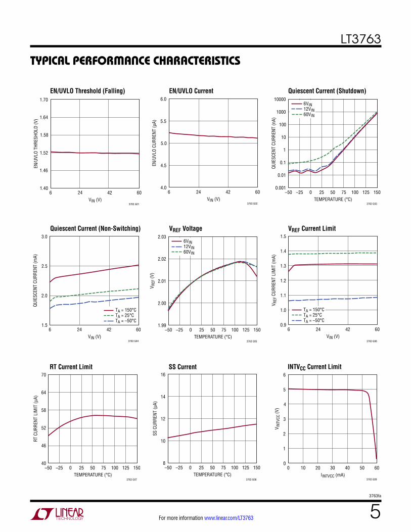
Typical perForMance characTerisTics
EN/UVLO Threshold (Falling) EN/UVLO Current Quiescent Current (Shutdown)
VIN (V)6
EN/U
VLO
THRE
SHOL
D (V
)
1.58
1.64
1.70
3763 G01
1.52
1.46
1.404224 60
VIN (V)6
EN/U
VLO
CURR
ENT
(µA)
5.0
5.5
6.0
42
3763 G02
4.5
4.024 60
TEMPERATURE (°C)–50
QUIE
SCEN
T CU
RREN
T (n
A)
100
1000
10000
75
3763 G03
10
1
0.001
0.01
0.1
–25 25 50 1501251000
6VIN12VIN60VIN
Quiescent Current (Non-Switching) VREF Voltage VREF Current Limit
VIN (V)
QUIE
SCEN
T CU
RREN
T (m
A)
3.0
2.0
3763 G04
2.5
1.5
TA = 150°CTA = 25°CTA = –50°C
6 4224 60TEMPERATURE (°C)
V REF
(V)
2.00
2.01
2.03
2.02
3763 G05
1.99–50 75–25 25 50 1501251000
6VIN12VIN60VIN
6 4224 60VIN (V)
V REF
CUR
RENT
LIM
IT (m
A)
1.2
1.4
1.5
3763 G06
1.0
1.3
1.1
0.9
TA = 150°CTA = 25°CTA = –50°C
RT Current Limit SS Current
TEMPERATURE (°C)
RT C
URRE
NT L
IMIT
(µA)
58
46
70
3763 G07
64
52
40–50 75–25 25 50 1501251000
TEMPERATURE (°C)
SS C
URRE
NT (µ
A)
16
14
12
10
3763 G08
8–50 75–25 25 50 1501251000
INTVCC Current Limit
IINTVCC (mA)0
V INT
VCC
(V)
4
5
6
50
3763 G09
3
1
2
010 20 4030 60

LT3763
63763fa
For more information www.linear.com/LT3763
Typical perForMance characTerisTics
INTVCC Load Regulation
Regulated Current vs VFB
Overvoltage Threshold Overvoltage Timeout
Maximum Output Voltage
VBOOST – VSW UVLO Thresholds INTVCC UVLO
TEMPERATURE (°C)
3.7
V BOO
ST –
VSW
(V)
3.8
3.9
4.0
4.1
4.2
3763 G11
–50 75–25 25 50 1501251000
RISING
FALLING
4.0
4.5
3.5
2.5
3.0
–50 75–25 25 50 1501251000TEMPERATURE (°C)
V INT
VCC
(V)
3763 G12
6VIN12VIN60VIN
IINTVCC (mA)0
V INT
VCC
(V)
5.00
5.05
5.10
40
3763 G13
4.95
4.9010 20 30 6050
VFB (V)1.16
–50
OUTP
UT C
URRE
NT (%
)
0
50
100
150
1.17 1.191.18 1.20
3763 G18
1.21
TEMPERATURE (°C)
V FB
(V)
1.47
1.49
1.55
1.53
1.51
3763 G14
1.45–50 75–25 25 50 1501251000
TEMPERATURE (°C)
TIM
EOUT
(µs)
12
13
14
3763 G15
11
10–50 75–25 25 50 1501251000
VIN – VOUT (V)0
OUTP
UT C
URRE
NT (%
)
75
100
125
2.0
3763 G17
50
25
00.5 1.0 1.5 2.5
VIN UVLO
TEMPERATURE (°C)
V IN
(V)
4.0
6.0
5.0
3763 G10
3.0–50 75–25 25 50 1501251000
Overcurrent Threshold
0
V SEN
SE+ –
VSE
NSE– (m
V)
20
40
60
100
80
3763 G16
–50 75–25 25 50 1501251000TEMPERATURE (°C)

LT3763
73763fa
For more information www.linear.com/LT3763
Typical perForMance characTerisTics
Regulated Sense Voltage
VCTRL1 (V)0
0
V SEN
SE+ –
VSE
NSE– (m
V)
10
20
30
40
50
60
0.5 1.0 1.5
3763 G25
2.0
Nonoverlap Time
Minimum On-TimeMinimum Off-Time
Current Regulation Accuracy
Current Regulation Accuracy
TG Driver RDS(ON) BG Driver RDS(ON)
TEMPERATURE (°C)
R DS(
ON) (
Ω)
3
4
3763 G19
2
1
0
PULL-UP
PULL-DOWN
–50 75–25 25 50 1501251000TEMPERATURE (°C)
R DS(
ON) (
Ω)
3
4
3763 G20
2
1
0
PULL-UP
PULL-DOWN
–50 75–25 25 50 1501251000 –50 75–25 25 50 1501251000TEMPERATURE (°C)
NONO
VERL
AP T
IME
(ns) 60
80
3763 G21
40
20
0
BG TO TG
TG TO BG
–50 75–25 25 50 1501251000TEMPERATURE (°C)
MIN
IMUM
ON-
TIM
E (n
s)
40
60
80
3763 G23
20
0
HG
LG
TEMPERATURE (°C)
MIN
IMUM
OFF
-TIM
E (n
s)
120
160
200
3763 G22
80
40
0
HG
LG
–50 75–25 25 50 1501251000
VOUT (V)0
–1.0
ACCU
RACY
(%)
–0.5
0
0.5
1.0
2 4 6 8 10
3763 G26
VCTRL1 = 1.5VVIN = 12V
VOUT (V)0
–1.0
ACCU
RACY
(%)
–0.5
0
0.5
1.0
2 4 6 8 10
3763 G27
VCTRL1 = 0.75VVIN = 12V
TEMPERATURE (°C)
FREQ
UENC
Y (M
Hz)
0.9
1.2
3763 G24
0.6
0.3
0
1MHz
500kHz
200kHz
–50 75–25 25 50 1501251000
Oscillator Frequency
LT3763
83763fa
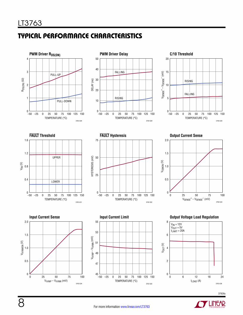
For more information www.linear.com/LT3763
FAULT Threshold Output Current SenseFAULT Hysteresis
Input Current Sense Output Voltage Load RegulationInput Current Limit
PWM Driver RDS(ON) C/10 ThresholdPWM Driver Delay
Typical perForMance characTerisTics
TEMPERATURE (°C)
R DS(
ON) (
Ω)
3
4
3763 G28
2
1
0
PULL-UP
PULL-DOWN
–50 75–25 25 50 1501251000TEMPERATURE (°C)
DELA
Y (n
s)
3763 G29
RISING
FALLING
–50 75–25 25 50 15012510000
10
20
30
40
50
TEMPERATURE (°C)
V SEN
SE+ –
VSE
NSE– (m
V) 15
20
3763 G30
10
5
0–50 75–25 25 50 1501251000
RISING
FALLING
TEMPERATURE (°C)
V FB
(V)
1.2
1.6
3763 G31
0.8
0.4
0–50 75–25 25 50 1501251000
UPPER
LOWER
TEMPERATURE (°C)
HYST
ERES
IS (m
V)
3763 G32
–50 75–25 25 50 15012510000
25
50
75
VSENSE+ – VSENSE
– (mV)0
0
V ISM
ON (V
)
0.5
1.0
1.5
2.0
25 50 75
3763 G33
100
VIVINP – VIVINN (mV)0
0
V IVI
NMON
(V)
0.5
1.0
1.5
2.0
25 50 75
3763 G34
100ILOAD (A)
00
V OUT
(V)
2
4
6
8
6 12 18
3763 G36
24
VIN = 12VVOUT = 5VILIMIT = 20A
TEMPERATURE (°C)
V IVI
NP –
VIV
INN
(mV)
3763 G35
–50 75–25 25 50 150125100045
47
49
51
53
55

LT3763
93763fa
For more information www.linear.com/LT3763
Shutdown and Recovery
PWM Dimming
15A Load Step
Output Voltage Load Regulation Efficiency vs Load CurrentEfficiency vs Load Current
Typical perForMance characTerisTics
ILOAD (A)0
0
V OUT
(V)
8
16
24
32
3 6 9
3763 G37
12
VIN = 48VVOUT = 24VILIMIT = 10A
ILOAD (A)0
EFFI
CIEN
CY (%
)
100
90
80
95
85
18
3763 G38
24126
VIN = 12VVOUT = 5V
ILOAD (A)0
EFFI
CIEN
CY (%
)
100
90
80
95
85
9
3763 G39
1263
VIN = 48VVOUT = 24V
SS2V/DIV
EN/UVLO5V/DIV
VOUT5V/DIV
IL5A/DIV
1ms/DIV 3763 G40
VOUT20mV/DIV
AC-COUPLED
IL10A/DIV
500µs/DIV 3763 G41
PWM10V/DIV
VSW50V/DIV
IL500mA/DIV
10µs/DIV 3763 G42
Solar Powered SLA Battery Charging
FAULT10V/DIV
VIN500mV/DIV
AC-COUPLED
VOUT50mV/DIV
AC-COUPLED
IL2A/DIV
50s/DIV 3763 G43
LT3763
103763fa
For more information www.linear.com/LT3763
BG (Pin 1): BG is the bottom FET gate drive signal that controls the state of the external low side power FET. The driver pull-up impedance is 2.2Ω, and pull-down imped-ance is 1Ω. Do not force any voltage on this pin.
INTVCC (Pin 2): The INTVCC pin provides a regulated 5V output for charging the BOOST capacitor. INTVCC also pro-vides the power for the digital and switching subcircuits. Do not force any voltage on this pin. Bypass with at least a 22µF capacitor to ground. INTVCC is current-limited to 50mA. Shutdown operation disables the output voltage drive.
VIN (Pin 3): Input Supply Pin. Must be locally bypassed with at least a 4.7µF low ESR capacitor to ground as close as possible to the exposed pad of the package.
EN/UVLO (Pin 4): Enable Pin. The EN/UVLO pin acts as an enable pin and turns on the internal current bias core and sub-regulators at 1.705V and turns off at 1.52V. The pin does not have any pull-up or pull-down, requiring a voltage bias for normal operation. Full shutdown occurs at approximately 0.5V. If unused, the Enable pin may be tied to VIN.
VREF (Pin 5): Buffered 2V Reference Capable of 0.5mA Drive. Bypass with at least 1µF capacitor to ground.
IVINN (Pin 6): IVINN is the inverting input of the input current sense amplifier. This pin connects to the drain of the high side N-channel power FET and the input current sense resistor.
IVINP (Pin 7): IVINP is the noninverting input of the input current sense amplifier. This pin connects to the input supply VIN and the input current sense resistor.
IVINMON (Pin 8): IVINMON is the buffered output of the input current sense amplifier. This pin enables monitoring of the averaged supply current with an output voltage of 20 • (VIVINP – VIVINN). The capacitive loading to this pin should be less than 1nF.
FAULT (Pin 9): Output Voltage Fault Detection Pin for Shorted or Open LEDs. Internal comparators pull down this pin when the FB pin voltage is lower than 0.25V or higher than 1.16V and when the inductor current is less than ten percent of the maximum value. This pin should be pulled up to INTVCC with a resistance higher than 10k.
FBIN (Pin 10): The FBIN pin enables peak power tracking for solar powered chargers and other similar applications by controlling the output current of the system based on the input voltage. This pin should be tied to VREF if this feature is not used.
FB (Pin 11): The feedback pin is used for voltage regula-tion and overvoltage protection. The feedback voltage is regulated to 1.206V. When the feedback voltage exceeds 1.515V, the overvoltage lockout prevents switching.
pin FuncTions
LT3763
113763fa
For more information www.linear.com/LT3763
pin FuncTionsGND (Pin 12, Pin 23, Pin 28, Exposed Pad Pin 29): Ground. The exposed pad must be soldered to the PCB.
CTRL2 (Pin 13): Thermal Control Input to Reduce the Regulated Output Current.
CTRL1 (Pin 14): The CTRL1 pin sets the regulated output current. The maximum control voltage is 1.5V. Above 1.5V, there is no change in the regulated current.
SS (Pin 15): The Soft-Start Pin. Place an external capacitor to ground to limit the regulated current during start-up conditions. The soft-start pin has an 11µA charging cur-rent. When the voltage at this pin is lower than voltages at CTRL1 and CTRL2, it overrides both signals and determines the regulated current.
SENSE– (Pin 16): SENSE– is the noninverting input of the error amplifier for the current regulation loop. The reference current, based on CTRL1, CTRL2, SS or FBIN determines the regulated voltage between SENSE+ and SENSE–.
SENSE+ (Pin 17): SENSE+ is the inverting input of the error amplifier for the current regulation loop. This pin is connected to an external current sense resistor. The voltage drop between SENSE+ and SENSE– is measured against the voltage drop across an internal resistor at the input to the current regulation loop.
VC (Pin 18): A resistor and capacitor connected in series to the VC pin provide the necessary compensation for the stability of the average current loop. Typical values are 5k to 60k for the resistor and 2.2nF to 10nF for the capacitor.
ISMON (Pin 19): ISMON is the buffered output of the output current sense amplifier. This voltage output enables monitoring the averaged output current of the LED driver with a voltage of 20 • (VSENSE
+ – VSENSE–). The capacitive
loading to this pin should be less than 1nF.
RT (Pin 20): A resistor from the RT pin to ground sets the switching frequency between 200kHz and 1MHz. When using the SYNC function, set the frequency to be at least 20% lower than the SYNC pulse frequency. This pin is current-limited to 55µA. Do not leave this pin open.
SYNC (Pin 21): Frequency Synchronization Pin. This pin allows the switching frequency to be synchronized to an external clock. The RT resistor should be chosen to oper-ate the internal clock at 20% slower than the SYNC pulse frequency. This pin should be grounded when not in use.
PWM (Pin 22): The input pin for PWM dimming of LEDs. When low, all switching is terminated and the PWM_OUT pin is low. This pin should be connected to INTVCC when not in use.
PWM_OUT (Pin 24): This pin can drive an external FET for PWM dimming of LEDs. The pull-up and pull-down impedances of the driver are 2.2Ω and 0.9Ω, respectively. Do not force any voltage on this pin.
TG (Pin 25): TG is the top FET gate drive pin that controls the state of the external high side power FET. The driver pull-up impedance is 2.2Ω, and pull-down impedance is 1.3Ω. Do not force any voltage on this pin.
SW (Pin 26): The SW pin is used internally as the lower rail for the floating top FET gate driver. Externally, this node connects the two power FETs and the inductor.
BOOST (Pin 27): The BOOST pin provides a floating 5V regulated supply for the top FET gate driver. An external schottky diode is required from the INTVCC pin to the BOOST pin to charge the BOOST capacitor when the SW pin is near ground.

LT3763
123763fa
For more information www.linear.com/LT3763
block DiagraM
–
+
8IVINMON
15SS
13CTRL2
+ –
+–
10FBIN
GND (12, 23, 28, 29)
1.206V
–
++14
CTRL1
–
+–
1.5V
1.5V
90k
11µA
3763 BD
CSS10nF
5VREF
VIN
CREF2.2µF
CFILT1µF
4EN/UVLO
VOUT
RFB212.1k
RFAULT47.5k
RFB147.5k
RFILTA1k
RFILTB1k
CURRENTMIRROR
INPUTCURRENT
MONITORINGgm = 400µA/V2V REFERENCE
OSCILLATOR
INTERNALREGULATORAND UVLO
50k
RS2.5mΩ
VOLTAGEREGULATOR AMP
gm = 850µA/V
CONTROLBUFFER
CIN14.7µF
CIN247µF
CVCC22µF
CBOOST200nF
L11µH
7
IVINP
6
IVINN
3
VIN
2
INTVCC BOOST
25TG
26SW
1BG
21SYNC
20RT
24PWM_OUT
22PWM
27
SYNCHRONOUSCONTROLLER
HIGH SIDEDRIVER
LOW SIDEDRIVER
R QS
+
–
RT82.5k
18VC
RC47.5k
CC4.7nF
–+
1.5V
1.206V
1.16V0.25V
+
–
19ISMON
+
–
0.1V
+–
17SENSE+
16SENSE–
11FB
9FAULT
OUTPUTMONITORING
C/10COMPARATOR
FAULTDETECTION
COMPARATORS
+ – + –
COUT200µF×2
INTVCC
3k
RSENSE_IN2.5mΩ
gm AMP gm = 475µA/VRO = 3.5MVCM(HIGH) = VIN – 1.4V
Figure 1. Block Diagram
LT3763
133763fa
For more information www.linear.com/LT3763
operaTionThe LT3763 utilizes fixed frequency, average current mode control to accurately regulate the inductor current inde-pendently from the output voltage. This is an ideal solution for applications requiring a regulated current source. The control loop will regulate the current in the inductor at an accuracy of ±6%. If the output reaches the regulation voltage determined by the resistor divider from the output to the FB pin, the inductor current will be reduced by the voltage regulation loop. In voltage regulation, the output voltage has an accuracy of ±1.5%. For additional opera-tion information, refer to the Block Diagram in Figure 1.
The current control loop has two main inputs, determined by the voltages at the analog control pins, CTRL1 and CTRL2. The lower voltage between CTRL1 and CTRL2 determines the regulated output current. The voltages at CTRL1 and CTRL2 are buffered to produce a reference current set by the voltage across an internal 90k resistor. This reference current produces a reference voltage that the average current mode control loop uses to regulate the inductor current as a voltage drop across the external sense resistor, RS. The outputs of the internal buffers are clamped at 1.5V, limiting the control range of the CTRL1 and CTRL2 pins from 0V to 1.5V—corresponding to a 0mV to 51mV range on RS.
The FBIN pin provides a third input to the current control loop. This input is dedicated to regulating the input volt-age by controlling the inductor current. Inductor current regulation commences when the voltage at the FBIN pin rises higher than 1.206V. Above 1.206V, the inductor current is linearly increased, providing the maximum current, as determined by the voltages at the CTRL pins, when FBIN is at and above 1.26V. When input voltage regulation is not needed, FBIN should be tied to VREF to allow the CTRL pins to control the inductor current.
The 2V reference provided on the VREF pin allows the use of a resistor voltage divider to the CTRL1 and CTRL2 pins. The current supplied by the VREF pin should be less than 0.5mA.
The error amplifier for the average current mode control loop has a common mode lockout that regulates the induc-tor current so that the error amplifier is never operated out of the common mode range. The common mode range is from ground to 1.4V below the VIN supply rail.
The LT3763 prevents excessive inductor current by trigger-ing overcurrent limit when the inductor current produces a voltage greater than 85mV across the SENSE+ and SENSE– pins. The current is limited on a cycle-by-cycle basis; switching shuts down as soon as the overcurrent level is reached. Overcurrent is not soft-started.
The regulated output voltage is set with a resistor divider from the output to the FB pin. The reference for the FB pin is 1.206V. If the output voltage level is high enough to engage the voltage loop, the regulated inductor current will be reduced. If the voltage at the FB pin reaches 1.515V, an internal overvoltage flag is set, shutting down switching for a brief period.
The EN/UVLO pin functions as a precision shutdown pin. When the voltage at the EN/UVLO pin is lower than 1.52V, the internal reset flag is asserted and switching is terminated. Full shutdown is guaranteed below 0.5V with a quiescent current of less than 2µA. The EN/UVLO pin has 185mV of hysteresis built in, and a 5µA current source is connected to this pin that allows any amount of hysteresis to be added with a series resistor or resistor divider from VIN. Alternatively, this pin can be tied directly to VIN to reduce the number of off-chip components.
During start-up, the SS pin is held low until the internal reset goes low and PWM goes high the first time after a reset event. Once the reset is cleared, the capacitor connected to the soft-start pin is charged with an 11μA current source. Initially, the internal buffers for the CTRL1, CTRL2, and FBIN voltages are limited by the voltage at the soft-start pin, and the inductor current reference slowly increases to the level determined by the lowest voltage of those three pins.
The rising threshold for thermal shutdown is set at 165°C with –5°C hysteresis. During thermal shutdown, all switch-ing is terminated, and the part is in reset mode (forcing the SS pin low).
The switching frequency is determined by a resistor at the RT pin. This pin is limited to 55µA, which limits the switching frequency to approximately 2MHz when the RT pin is shorted to ground. The LT3763 may also be synchronized to an external clock through the use of the

LT3763
143763fa
For more information www.linear.com/LT3763
operaTionSYNC pin which has precise thresholds at 2.175V and 1.5V for rising and falling edges, respectively.
LT3763 also features a PWM driver for LED dimming. PWM_OUT is high when the PWM pin voltage is higher than 2.175V, and low when PWM is lower than 1.5V. Switching is terminated when PWM is lower than 1.5V. PWM should be tied to INTVCC when the PWM function is not needed.
The FAULT pin is pulled down to ground when the voltage at FB becomes less than 0.25V which indicates a short-circuit condition. It is also pulled down to indicate an open-circuit condition when the voltage becomes greater than 1.16V and the inductor current is less than ten percent of the maximum (C/10), or equivalently, when the volt-age between SENSE+ and SENSE– is less than 5mV. To avoid jitter when recovering from a fault condition, 50mV hysteresis is employed in the comparators. Additionally, when the inductor current is lower than C/10, the C/10 comparator disables the low side MOSFET regardless of the voltage at FB.
The integrated input current and output current monitor-ing functions of the LT3763 allow users to acquire system
information such as the input power and output power. The outputs of the current monitors, IVINMON and ISMON, range from 0V to 1V when the inputs vary from 0V to 50mV. When using 2.5mΩ sense resistors, for example, these current monitoring amplifiers sense from 0A to 20A. To filter out the switching portion of the currents and measure the average current information, the input pins of the input current monitor, IVINP and IVINN, should connect to the sense resistor through two 1k resistors and a capacitor directly between the IVINP and IVINN pins. The capacitance value can be adjusted according to the switching frequency and the ripple magnitude. The output current monitor employs an internal filter to reduce ripple, and it does not require an external filter, but if one is added, the corner frequency should be higher than the switching frequency.
The LT3763 also includes an input current limiting func-tion to regulate the input current to a value determined by the RSENSE_IN resistor. When the voltage drop across the RSENSE_IN resistor approaches 50mV, the inductor current is reduced and regulated so that 50mV is maintained across the IVINP and IVINN pins.
applicaTions inForMaTionProgramming Inductor Current
The analog voltage at the CTRL1 pin is buffered and pro-duces a reference voltage, VCTRL, across an internal resistor. The regulated average inductor current is determined by:
IO = VCTRL
30 •RS
where RS is the external sense resistor and IO is the aver-age inductor current, which is equal to the output current. Figure 2 shows the maximum output current versus RS. The maximum power dissipation in the resistor will be:
PRS =
0.05V( )2RS
Figure 3 plots the power dissipation in RS, and Table 1 lists several resistance values and the corresponding
Figure 2. RS Value Selection for Regulated Output Current
maximum inductor current and sense-resistor power dis-sipation. Susumu, Panasonic and Vishay offer accurate sense resistors.
RS (mΩ)
0
MAX
IMUM
OUT
PUT
CURR
ENT
(A)
10
20
30
5
15
25
4 8 12 16
3763 F02
2020 6 10 14 18

LT3763
153763fa
For more information www.linear.com/LT3763
applicaTions inForMaTion
Table 1. Sense Resistor ValuesMAXIMUM OUTPUT
CURRENT (A) RESISTOR, RS (mΩ) POWER DISSIPATION (W)
1 50 0.05
5 10 0.25
10 5 0.50
25 2 1.25
Inductor Selection
Size the inductor so that the peak-to-peak ripple current is approximately 30% of the output current.
The following equation sizes the inductor for best per-formance:
L = VIN • VO – VO
2
0.3 • fSW •IO • VIN
⎛
⎝⎜
⎞
⎠⎟
where VO is the output voltage, VIN is the input voltage, IO is the maximum regulated current in the inductor and fSW is the switching frequency.
The overcurrent comparator terminates switching when the voltage between the SENSE+ and SENSE– pins exceeds 85mV. The saturation current for the inductor should be at least 20% higher than the maximum regulated current. Recommended inductor manufacturers are listed in Table 2.
Figure 3. Power Dissipation in RS
Table 2. Recommended Inductor ManufacturersVENDOR WEBSITE
Coilcraft www.coilcraft.com
Sumida www.sumida.com
Vishay www.vishay.com
Würth Electronics www.we-online.com
NEC-Tokin www.nec-tokin.com
Switching MOSFET Selection
The following parameters are critical in determining the best switching MOSFETs for a given application: total gate charge (QG), on-resistance (RDS(ON)), gate to drain charge (QGD), gate-to-source charge (QGS), gate resistance (RG), breakdown voltages (maximum VGS and VDS) and drain current (maximum ID). The following guidelines provide information to make the selection process easier, and Table 3 lists some recommended parts and manufacturers.
For both switching MOSFETs the rated drain current should be greater than the maximum inductor current. Use the following equation to calculate the peak inductor current:
IMAX = IO +
VIN • VO – VO2
2 • fSW •L • VIN
⎛
⎝⎜
⎞
⎠⎟
The rated drain current is temperature dependent, and most data sheets include a table or graph of the rated drain current versus temperature.
The rated VDS should be higher than the maximum input voltage (including transients) for both MOSFETs. As for the rated VGS, the signals driving the gates of the switching MOSFETs have a maximum voltage of 5V with respect to the source. However, during start-up and recovery conditions, the gate-drive signals may be as low as 3V. Therefore, to ensure that the LT3763 recovers properly, the maximum threshold voltage should be less than 2V, and for a robust design, ensure that the rated VGS is greater than 7V.
Power losses in the switching MOSFETs are related to the on-resistance, RDS(ON); gate resistance, RG; gate-to-drain charge, QGD and gate-to-source charge, QGS. Power lost to the on-resistance is an Ohmic loss, I2RDS(ON), and usually dominates for input voltages less than 15V. Power lost while charging the gate capacitance dominates for voltages
RS (mΩ)0
0
POW
ER D
ISSI
PATI
ON (W
)
0.2
0.6
0.8
1.0
1.4
2 10 14
3763 F03
0.4
1.2
8 18 204 6 12 16

LT3763
163763fa
For more information www.linear.com/LT3763
INPUT VOLTAGE (V)0
4
5
7
30
3763 F04a
3
2
10 20 40
1
0
6
MOS
FET
POW
ER L
OSS
(W)
TOTAL
OHMIC
TRANSITIONAL
INPUT VOLTAGE (V)0
MOS
FET
POW
ER L
OSS
(W)
1.0
1.5
40
3763 F04b
0.5
010 20 30
2.5
2.0
TOTAL
OHMIC
TRANSITIONAL
applicaTions inForMaTiongreater than 15V. When operating at higher input voltages, efficiency can be optimized by selecting a high side MOSFET with higher RDS(ON) and lower QG. The total power loss in the high side MOSFET can be approximated by:
PLOSS = ohmic loss + transition loss
PLOSS ≈VOVIN
•IO2RDS(ON) •ρT
⎛⎝⎜
⎞⎠⎟+
VIN •IOUT5V
⎛⎝⎜
⎞⎠⎟ •
QGD +QGS( ) •
2 •RG +RPU+RPD( )⎛
⎝⎜
⎞
⎠⎟ • fSW
⎛
⎝⎜⎜
⎞
⎠⎟⎟
where rT is a dimensionless temperature dependent factor in the MOSFET’s on-resistance. Using 70°C as the maximum ambient operating temperature, rT is roughly equal to 1.3. RPD and RPU are the LT3763 high side gate driver output impedances: 1.3Ω and 2.2Ω, respectively.
A good approach to MOSFET sizing is to select a high side MOSFET, then select the low side MOSFET. The trade-off between RDS(ON), QG, and QGS for the high side MOSFET is evident in the following example. VO is equal to 4V. These two N-channel MOSFETs are rated for a VDS of 40V and mounted in the same package, but with 8× different RDS(ON) and 4.5× different QG and QGD:
M1: RDS(ON) = 2.3mΩ, QG = 45.5nC,
QGS = 13.8nC, QGD = 14.4nC, RG = 1Ω
M2: RDS(ON) = 18mΩ, QG = 10nC,
QGS = 4.5nC, QGD = 3.1nC, RG = 3.5Ω
Power loss for both MOSFETs is shown in Figure 4. Observe that whereas the RDS(ON) of M1 is eight times lower, the power loss at low input voltages is about equal to that of M2, and at high voltages, it is four times higher.
Power loss within the low side MOSFET is almost entirely from the RDS(ON) of the FET. Select the low side FET with the lowest RDS(ON) while keeping the total gate charge QG to 30nC or less.
Another power loss related to switching MOSFET selection is the power lost driving the gates. The total gate charge,
QG, must be charged and discharged each switching cycle, so the power lost to the charging of the gates is:
PGATE = VIN • (QGLG + QGHG) • fSW
where QGLG is the low side gate charge and QGHG is the high side gate charge.
The majority of this loss occurs in the internal LDO within the LT3763:
PLOSS_LDO ≈ (VIN – 5V) • (QGLG + QGHG) • fSW
Whenever possible, utilize a switching MOSFET that minimizes the total gate charge to limit the internal power dissipation of the LT3763. Some recommended MOSFETs are listed in Table 3.
Figure 4a. Power Loss Example for M1
Figure 4b. Power Loss Example for M2

LT3763
173763fa
For more information www.linear.com/LT3763
Table 3. Recommended Switching FETsVIN (V)
VOUT (V)
IOUT (A) TOP FET BOTTOM FET MANUFACTURER
60 4 20 RJK0853DPB RJK0853DPB Renesas www.renesas.com24 4 5 RJK0368DPA RJK0332DPB
48 10 to 35 10 RJK0851DPB RJK0851DPB
12 2 to 4 10 FDMS8680 FDMS8672AS Fairchild www.fairchildsemi.com
26 4 20 Si7884BDP SiR470DP Vishay www.vishay.com
24 4 40 PSMN4R0-30YL RJK0346DPA NXP/Philips www.nxp.com
36 12 10 BSC100N06LS3 BSC100N06LS3 www.infineon.com
Input Capacitor Selection
The input capacitor should be sized at least 2µF for every 1A of output current and placed very close to the high side MOSFET. The loop created by the input capacitor, high side MOSFET, low side MOSFET should be minimized. It should have a ripple current rating equal to half of the maximum output current. Additionally, a small 4.7µF ceramic capaci-tor should be placed between VIN and ground as close as possible to the VIN pin and the exposed pad of the package for optimal noise immunity.
It is recommended that several low ESR (equivalent se-ries resistance) ceramic capacitors be used as the input capacitance, although other capacitors with higher density may be required to reduce board area. Only X5R or X7R capacitors maintain their capacitance over a wide range of operating voltages and temperatures.
Output Capacitor Selection
The output capacitors need to have very low ESR to reduce output ripple. A minimum of 20µF/A of load current should be used in most designs. The capacitors also need to be surge rated to the maximum output current. To achieve the lowest possible ESR, several low ESR ceramic capaci-tors should be used in parallel. Many lower output voltage applications benefit from the use of high density POSCAP capacitors, which are easily destroyed when exposed to overvoltage conditions. To prevent this, select POSCAP capacitors that have a voltage rating that is at least 50% higher than the regulated voltage.
Note that when dimming, the output voltage increases at the
applicaTions inForMaTionend of every pulse as the decreasing inductor current flows into the output capacitor. Use of a small output capacitor may trigger overvoltage protection through the FB pin.
CBOOST Capacitor Selection
The CBOOST capacitor must be sized no bigger than 220nF and more than 50nF to ensure proper operation of the LT3763. Use 220nF for high current switching MOSFETs with high gate charge.
INTVCC Capacitor Selection
The bypass capacitor for the INTVCC pin should be larger than 22µF to ensure stability, and it should be connected as close as possible to the exposed pad underneath the package. It is recommended that the ESR be lower than 50mΩ to reduce noise within the LT3763. For driv-ing MOSFETs with gate charges larger than 44nC, use 0.5µF/nC of total gate charge.
Soft-Start
Unlike conventional voltage regulators, the LT3763 utilizes the soft-start function to control the regulated inductor current instead of the output voltage. The charging current is 11µA and reduces the set current as long as the SS pin voltage is lower than CTRL1 and CTRL2.
Output Current Regulation
To adjust the regulated load current, an analog voltage is applied to the CTRL1 pin. Figure 5 shows the regulated voltage across the sense resistor for control voltages up to
VCTRL1 (V)0
0
V SEN
SE+ –
VSE
NSE– (m
V)
10
20
30
40
50
60
0.5 1.0 1.5
3763 F05
2.0
Figure 5. Sense Voltage vs CTRL Voltage

LT3763
183763fa
For more information www.linear.com/LT3763
applicaTions inForMaTion
Figure 6. Analog Control of Inductor Current
Figure 7. Input Current Monitoring Voltage vs Input Current Sense Voltage
Figure 8. Output Current Monitoring Voltage vs Output Current Sense Voltage
Figure 9. Output Voltage Regulation and Overvoltage Protection Feedback Connections
2V. Figure 6 shows the CTRL1 voltage created by a voltage divider from VREF to ground. When sizing the resistor divider, please be aware that the VREF pin should have a total load current less than 0.5mA, and that above 1.5V, the control voltage has no effect on the regulated inductor current. Setting CTRL1 to 0V does not automatically stop switch-ing. To disable switching, set PWM pin voltage below 1.5V.
Input Current Monitoring
Users can monitor the input current at the IVINMON pin, which produces 0V to 1V as the voltage between IVINP and IVINN varies from 0mV to 50mV, as shown in Figure 7. Due to the switching of the high side FET, the input current is noisy and monitoring the average input current requires an external filter with 1k resistors connecting IVINP and IVINN to the input current sense resistor RSENSE_IN. Choose the capacitor for this filter according to the switching frequency so that the noise is reduced by at least a factor of 100. If the frequency is 500kHz, for example, 1µF is sufficient, and higher switching frequencies will require a smaller capacitor. A resistor and capacitor may be connected to IVINMON to further filter the noise. With both input and
LT3763
VREF
R2
R1
3763 F06
CTRL1
output current monitoring, the LT3763 enables users to calculate the overall efficiency of the circuit including the losses in the external components.
Output Current Monitoring
The LT3763 provides users the capability to monitor the output current as a voltage provided at the ISMON pin. The voltage will linearly increase from 0V to 1V as the voltage between SENSE+ and SENSE– increases from 0mV to 50mV as shown in Figure 8. If, for example, a 2.5mΩ resistor is chosen for RS, then a 1V output at ISMON will indicate a 20A output current. A resistor and capacitor may be connected to ISMON to filter noise.
Voltage Regulation and Overvoltage Protection
The LT3763 uses the FB pin to regulate the output volt-age and to provide an overvoltage lockout to avoid high voltage conditions. The regulated output voltage is pro-grammed using a resistor divider from the output to the FB pin (Figure 9). When the output voltage approaches
VIVINP – VIVINN (mV)0
0
V IVI
NMON
(V)
0.5
1.0
1.5
2.0
25 50 75
3763 F07
100
VSENSE+ – VSENSE
– (mV)0
0
V ISM
ON (V
)
0.5
1.0
1.5
2.0
25 50 75
3763 F08
100
LT3763 R2
VOUT
R1
3763 F09
FB

LT3763
193763fa
For more information www.linear.com/LT3763
applicaTions inForMaTionthe programmed level (1.206V at the FB pin), the voltage error amplifier overrides CTRL1 to set the inductor cur-rent and regulate VOUT. When the output voltage exceeds 125% of the regulated voltage level (1.515V at the FB pin), the internal overvoltage flag is set, terminating switching. The regulated output voltage must be greater than 1.5V and is set by the equation:
VOUT =1.206V 1+R2
R1⎛⎝⎜
⎞⎠⎟
Fault Detection
The LT3763 detects that the load has had an open-circuit or short-circuit event indicated by pulling the FAULT pin to ground. These conditions are detected by comparing the voltage at the FB pin to two internal reference voltages. A short-circuit is defined as VFB lower than 0.25V. In an open-circuit condition, the regulated inductor current will charge the output capacitor, the voltage at FB will begin to increase, and the voltage error amplifier will begin to reduce the inductor current. The open-circuit condition will be indicated at FAULT when FB is higher than 1.16V and the inductor current is less than ten percent (C/10) of the maximum value set by the sense resistor RS. The output voltage will be regulated as determined by the resistor divider to the FB pin.
Low Current Detection
When the inductor current decreases to ten percent of the maximum current, the C/10 comparator will also disable the low side gate driver, so the converter will become non-synchronous and automatically transition into dis-continuous conduction mode when the inductor current is low enough relative to the ripple.
The low current condition is an essential part of battery charging applications. The LT3763 works well in this ap-plication delivering a constant current to the battery as it charges and then automatically reducing the current to a trickle charge as the battery voltage approaches its fully charged value. In this application, the signal at FAULT triggered by the low current detection comparator serves as an indicator that the trickle charge phase of charging the battery has begun.
Programming Switching Frequency
The LT3763 has an operational switching frequency range between 200kHz and 1MHz. This frequency is programmed with an external resistor from the RT pin to ground. Do not leave this pin open under any condition. The RT pin is also current-limited to 55µA. See Table 4 and Figure 10 for resis-tor values and the corresponding switching frequencies.
Table 4. Switching FrequencySWITCHING FREQUENCY (MHz) RT (kΩ)
1.00 40.2
0.75 53.6
0.50 82.5
0.30 143
0.20 221
Switching Frequency Synchronization
The nominal switching frequency of the LT3763 is deter-mined by the resistor from the RT pin to ground and may be set from 200kHz to 1MHz. The internal oscillator may also be synchronized to an external clock through the SYNC pin. The external clock applied to the SYNC pin must have a logic low below 1.5V and a logic high above 2.175V. The input frequency must be 20% higher than the frequency that would otherwise be determined by the resistor at the RT pin. Input signals outside of these specified parameters will cause erratic switching behavior and subharmonic oscillations. Synchronization is tested at 500kHz with a 221k RT resistor. Operation under other conditions is guaranteed by design. When synchronizing to an external
RT (kΩ)
0.0
FREQ
UENC
Y (M
Hz)
0.4
0.8
1.2
0.2
0.6
1.0
100 150 200
3763 F10
250500
Figure 10. Frequency vs RT Resistance
LT3763
203763fa
For more information www.linear.com/LT3763
applicaTions inForMaTion
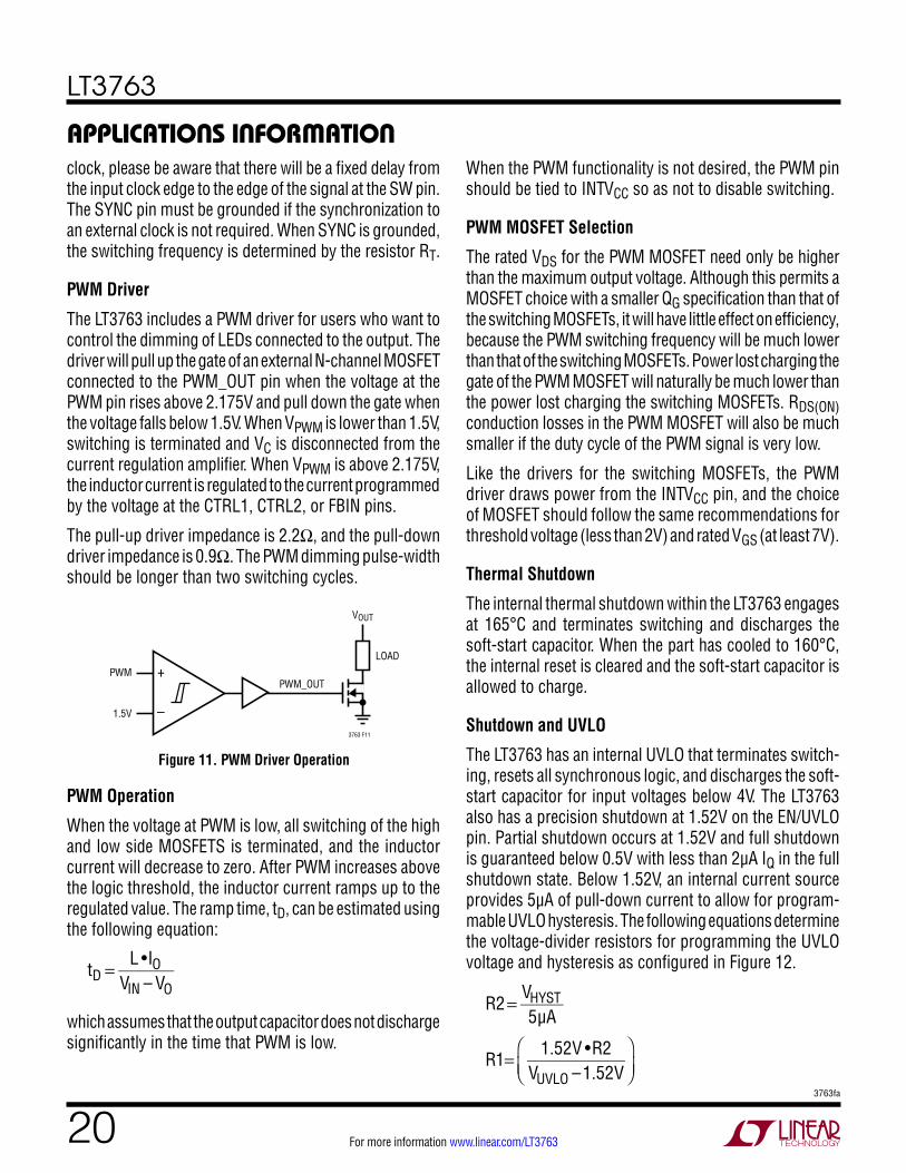
Figure 11. PWM Driver Operation
clock, please be aware that there will be a fixed delay from the input clock edge to the edge of the signal at the SW pin. The SYNC pin must be grounded if the synchronization to an external clock is not required. When SYNC is grounded, the switching frequency is determined by the resistor RT.
PWM Driver
The LT3763 includes a PWM driver for users who want to control the dimming of LEDs connected to the output. The driver will pull up the gate of an external N-channel MOSFET connected to the PWM_OUT pin when the voltage at the PWM pin rises above 2.175V and pull down the gate when the voltage falls below 1.5V. When VPWM is lower than 1.5V, switching is terminated and VC is disconnected from the current regulation amplifier. When VPWM is above 2.175V, the inductor current is regulated to the current programmed by the voltage at the CTRL1, CTRL2, or FBIN pins.
The pull-up driver impedance is 2.2Ω, and the pull-down driver impedance is 0.9Ω. The PWM dimming pulse-width should be longer than two switching cycles.
When the PWM functionality is not desired, the PWM pin should be tied to INTVCC so as not to disable switching.
PWM MOSFET Selection
The rated VDS for the PWM MOSFET need only be higher than the maximum output voltage. Although this permits a MOSFET choice with a smaller QG specification than that of the switching MOSFETs, it will have little effect on efficiency, because the PWM switching frequency will be much lower than that of the switching MOSFETs. Power lost charging the gate of the PWM MOSFET will naturally be much lower than the power lost charging the switching MOSFETs. RDS(ON) conduction losses in the PWM MOSFET will also be much smaller if the duty cycle of the PWM signal is very low.
Like the drivers for the switching MOSFETs, the PWM driver draws power from the INTVCC pin, and the choice of MOSFET should follow the same recommendations for threshold voltage (less than 2V) and rated VGS (at least 7V).
Thermal Shutdown
The internal thermal shutdown within the LT3763 engages at 165°C and terminates switching and discharges the soft-start capacitor. When the part has cooled to 160°C, the internal reset is cleared and the soft-start capacitor is allowed to charge.
Shutdown and UVLO
The LT3763 has an internal UVLO that terminates switch-ing, resets all synchronous logic, and discharges the soft-start capacitor for input voltages below 4V. The LT3763 also has a precision shutdown at 1.52V on the EN/UVLO pin. Partial shutdown occurs at 1.52V and full shutdown is guaranteed below 0.5V with less than 2µA IQ in the full shutdown state. Below 1.52V, an internal current source provides 5µA of pull-down current to allow for program-mable UVLO hysteresis. The following equations determine the voltage-divider resistors for programming the UVLO voltage and hysteresis as configured in Figure 12.
R2= VHYST5µA
�
R1= 1.52V •R2VUVLO –1.52V
⎛⎝⎜
⎞⎠⎟
PWM Operation
When the voltage at PWM is low, all switching of the high and low side MOSFETS is terminated, and the inductor current will decrease to zero. After PWM increases above the logic threshold, the inductor current ramps up to the regulated value. The ramp time, tD, can be estimated using the following equation:
tD = L •IO
VIN – VO
which assumes that the output capacitor does not discharge significantly in the time that PWM is low.
3763 F11
–
+
VOUT
PWM_OUT
LOAD
PWM
1.5V

LT3763
213763fa
For more information www.linear.com/LT3763
applicaTions inForMaTion
Figure 12. UVLO Configuration
Figure 13. Load Current Derating vs Temperature Using NTC Resistor
Figure 14. LT3763 Average Current Mode Control Scheme
LT3763
VIN
R2
VIN
R1
3763 F12
EN/UVLO
Load Current Derating Using the CTRL2 Pin
The LT3763 is designed specifically for driving high power loads. In high current applications, derating the maxi-mum current based on operating temperature prevents damage to the load. In addition, many applications have thermal limitations that will require the regulated current to be reduced based on load temperature and/or board temperature. To achieve this, the LT3763 uses the CTRL2 pin to reduce the effective regulated current in the load, which is otherwise programmed by the analog voltage at the CTRL1 pin. The load/board temperature derating is programmed using a resistor divider with a temperature dependant resistance (Figure 13). When the load/board temperature rises, the CTRL2 voltage will decrease. When the CTRL2 voltage is lower than voltage at the CTRL1 pin, the regulated current is reduced.
LT3763
VREF
RNTC RX
RV RV
R2
R1(OPTION A TO D)
3763 F13CTRL2
B
RNTC
A
RNTC RX
D
RNTC
C
Average Current Mode Control Compensation
The use of average current mode control allows for pre-cise regulation of the inductor current and load current. Figure 14 shows the average current mode control loop used in the LT3763, where the regulation current is pro-grammed by a current source and a 3k resistor.
To design the compensation network, the maximum com-pensation resistor needs to be calculated. In current mode controllers, the ratio of the sensed inductor current ramp
–
+gm
ERROR AMP
MODULATOR
LOAD
RC
L RS
3kVCTRL • 11µA/V
CC
3763 F14
to the slope compensation ramp determines the stability of the current regulation loop above 50% duty cycle. In the same way, average current mode controllers require the slope of the error voltage to not exceed the PWM ramp slope during the switch off time.
Since the closed loop gain at the switching frequency produces the error signal slope, the output impedance of the error amplifier will be the compensation resistor, RC. Use the following equation as a good starting point for compensation component sizing:
RC =
1kΩ •1V •LVO •RS • TSW
,�CC =2nFµs
• TSW
LT3763
223763fa
For more information www.linear.com/LT3763
applicaTions inForMaTionwhere TSW is the switching period, L is the inductance value, VO is the output voltage and RS is the sense resistor. For most applications, a 4.7nF compensation capacitor is adequate and provides excellent phase margin with optimized bandwidth. Please refer to Table 6 for recom-mended compensation values.
Board Layout Considerations
Average current mode control is relatively immune to the switching noise associated with other types of control schemes. Nevertheless, the high di/dt loop formed by input
Table 6. Recommended Compensation Component Values (VCTRL2 = 2V)VIN (V) VO (V) VCTRL1 (V) IL (A) fSW (kHz) L (µH) RS (mΩ) RC (kΩ) CC (nF)
12 4 0.75 5 500 2.2 5 54.9 4.7
12 4 1.50 10 500 2.2 5 54.9 4.7
12 5 1.50 20 250 2.2 2.5 44.2 8.2
60 30 0.15 1 500 10 5 15.4 4.7
60 30 1.20 8 500 10 5 15.4 4.7
capacitors and switching MOSFETS should be minimized. Placing the sense resistor as close as possible to the SENSE+ and SENSE– pins also helps avoid noise issues. Due to sense resistor ESL (equivalent series inductance), 10Ω resistors in series with the SENSE+ and SENSE– pins with a 33nF ca-pacitor placed between the SENSE pins are recommended. Utilizing a good ground plane underneath the switching components will minimize interplane noise coupling. To dissipate the heat from the switching components, use a large area for the switching node while keeping in mind that this negatively affects the radiated noise.
LT3763
233763fa
For more information www.linear.com/LT3763
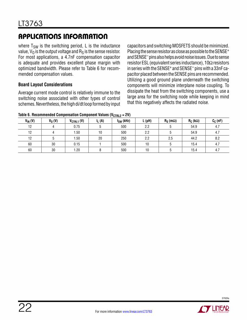
Typical applicaTions20A, Pulse Width Modulated, Single LED Driver
CIN2100µF
VIN10V TO 30V
RSENSE_IN2.5mΩ
RFILTA1k
RFILTB1k
RT82.5k
EN/UVLO
FBIN
TG
VIN
BOOST
VREF
CTRL1
CTRL2LT3763
SW
BG
GND
VC
SENSE+
SENSE–
INTVCC
CBOOST220nF L1
1.5µH
CVCC22µF
RS2.5mΩ
FB
FAULT
RC59k
CC4.7nF
RFB147.5k
L1: COILCRAFT XAL1010-152M1: RENESAS RJK0365M2: RENESAS RJK0453M3: IR IRFH6200RS: VISHAY WSL25122L500FEA
3763 TA02
RFB212.1k
CREF2.2µF
RNTC470k
M1
M2
PWMOUT M3
VOUT6V, 20A MAXIMUM
COUT220µF×2
D1
PWMSYNC
SS
CSS10nF
RT
RHOT45.3k
REN184.5k
REN215.4k
CS33nF
RSA10Ω
RSB10Ω
RFAULT47.5kΩ
CFILT1µF
50k
CIN14.7µF
IVINNIVINP
IVINMON
ISMON1nF
1nF
50Ω
50Ω
PWM Dimming
PWM10V/DIV
VSW50V/DIV
IL5A/DIV
5µs/DIV 3763 TA02b

LT3763
243763fa
For more information www.linear.com/LT3763
Typical applicaTions1A, Five LED Driver
CIN24.7µF
VIN32V TO 60V
RSENSE_IN50mΩ
RFILTA1k
RFILTB1k
RT82.5k
EN/UVLO
FBIN
TG
VIN
BOOSTVREF
CTRL1
CTRL2
LT3763SW
BG
GND
VC
SENSE+
SENSE–
INTVCC
INTVCC
ENABLECBOOST
50nF L1100µH
CVCC22µF
RS50mΩ
FB
FAULT
RC59k
CC4.7nF
RFB1287k
L1: COILCRAFT MSS1278-104M1, M2: RENESAS RJK1054RS: VISHAY WSL2512R0500FEA 3763 TA03
RFB212.1k
CREF2.2µF
RNTC470k
M1
M2
PWMOUT
VOUT30V, 1A MAXIMUM
COUT10µF×2D1
D2
D3
D4
D5
PWMSYNC
SS
CSS10nF
RT
RHOT45.3k
CS33nF
RSA10Ω
RSB10Ω
RFAULT47.5kΩ
CFILT1µF
50k
CIN11µF
IVINNIVINP
IVINMON
ISMON

LT3763
253763fa
For more information www.linear.com/LT3763
3.3A, Six-Cell (36V) SLA Battery Charger
CIN247µF
VIN48V
RSENSE_IN15mΩ
RFILTA1k
RFILTB1k
RT82.5k
EN/UVLOENABLE
FBIN
TG
VIN
BOOSTVREF
CTRL1
CTRL2
LT3763SW
BG
GND
VC
SENSE+
SENSE–
INTVCC
INTVCC
CBOOST220nF L1
12µH
CVCC22µF
COUT10µF
RS15mΩ
FB
FAULT
RC8.06k
CC4.7nF
RFB1402k
RFB3178k
12V
L1: WÜRTH 74471112M1, M2: INFINEON BSC100N06LS3M3: VISHAY VN2222LLRS: VISHAY WSL2512R0150
3763 TA04
RFB212.1k
CREF2.2µF
M1
M2
M3
PWMOUT
VOUT45V, 3.3A MAXIMUM
PWMSYNC
SS
CSS10nF
RT
CS33nF
RSA10Ω
RSB10Ω
RFAULT47.5kΩ
CFILT1µF
+
12V+
12V+
CIN11µF
IVINNIVINP
IVINMON
ISMON
Typical applicaTions
36V SLA Battery Charging
FAULT10V/DIV
VOUT50mV/DIV
AC-COUPLED
IL2A/DIV
50s/DIV 3763 TA04b

LT3763
263763fa
For more information www.linear.com/LT3763
Typical applicaTions
20A, Synchronized, 5V Regulator
CIN2100µF
VIN7V TO 30V
RSENSE_IN2.5mΩ
RFILTA1k
RFILTB1k
RT121k
EN/UVLO
FBIN
TG
VIN
BOOSTVREF
CTRL1
CTRL2
LT3763SW
BG
GND
VC
SENSE+
SENSE–
INTVCC
INTVCC
CBOOST220nF L1
1.5µH
CVCC22µF
RS2.5mΩ
FB
FAULT
RC59k
CC4.7nF
RFB138.3k
L1: COILCRAFT XAL1010-152M1: RENESAS RJK0365M2: RENESAS RJK0453RS: VISHAY WSL25122L500FEA
3763 TA05
RFB212.1k
CREF2.2µF
RNTC470k
M1
M2
PWMOUT
VOUT5V, 20A MAXIMUM
COUT220µF×2
PWMSYNC
SS
CSS10nF
RT
RHOT45.3k
CS33nF
RSA10Ω
RSB10Ω
RFAULT47.5kΩ
CFILT1µF
3V0V
500kHz
CIN14.7µF
IVINNIVINP
IVINMON
ISMON
REN144.2k
REN215.4k
Output Voltage Load Regulation Efficiency vs Load Current
ILOAD (A)0
EFFI
CIEN
CY (%
)
100
90
80
95
85
18
3763 TA05c
24126
VIN = 12VVOUT = 5V
ILOAD (A)0
0
V OUT
(V)
2
4
6
8
6 12 18
3763 TA05b
24
VIN = 12VVOUT = 5VILIMIT = 20A

LT3763
273763fa
For more information www.linear.com/LT3763
Typical applicaTions
350W White LED Driver
CIN2100µF
VIN48V
RT200k
EN/UVLO
FBIN
TG
VIN
BOOSTVREF
CTRL1
CTRL2
LT3763SW
BG
GND
VC
SENSE+
SENSE–
INTVCC
INTVCC
CBOOST220nF L1
6µH
50k
CVCC22µF
RS5mΩ
FB
FAULT
RC5k
CC5nF
RFB1931k
L1: COILTRONICS HC2-6R0M1, M2: RENESAS RJK0851RS: VISHAY WSL25125L000
LUMINUSPT-121
3763 TA06
RFB230.9k
CREF2.2µF
M1×2
M2×2
PWMOUT
VOUT37V, 10A MAXIMUM
COUT10µF×6
PWMSYNC
SS
CSS10nF
RT
CS1nF
RFAULT100k
3V0V
400kHz
CIN14.7µF
IVINNIVINP
IVINMON
ISMON
REN1374k
REN2124k
Maximum Output Voltage Efficiency vs LED Current
ILED (A)0
EFFI
CIEN
CY (%
)
100
90
80
95
85
9
3763 TA06c
1263
VIN = 48VVOUT = 35V
ILED (A)0
0
V OUT
(V)
10
20
30
40
3 6 9
3763 TA06b
12
VIN = 48VILIMIT = 10A

LT3763
283763fa
For more information www.linear.com/LT3763
package DescripTionPlease refer to http://www.linear.com/designtools/packaging/ for the most recent package drawings.
FE28 (EB) TSSOP REV I 0211
0.09 – 0.20(.0035 – .0079)
0° – 8°
0.25REF
0.50 – 0.75(.020 – .030)
4.30 – 4.50*(.169 – .177)
1 3 4 5 6 7 8 9 10 11 12 13 14
192022 21 151618 17
9.60 – 9.80*(.378 – .386)
4.75(.187)
2.74(.108)
28 27 26 2524 23
1.20(.047)MAX
0.05 – 0.15(.002 – .006)
0.65(.0256)
BSC0.195 – 0.30
(.0077 – .0118)TYP
2RECOMMENDED SOLDER PAD LAYOUT
EXPOSEDPAD HEAT SINKON BOTTOM OF
PACKAGE0.45 ±0.05
0.65 BSC
4.50 ±0.10
6.60 ±0.10
1.05 ±0.10
4.75(.187)
2.74(.108)
MILLIMETERS(INCHES) *DIMENSIONS DO NOT INCLUDE MOLD FLASH. MOLD FLASH
SHALL NOT EXCEED 0.150mm (.006") PER SIDE
NOTE:1. CONTROLLING DIMENSION: MILLIMETERS2. DIMENSIONS ARE IN
3. DRAWING NOT TO SCALE
SEE NOTE 4
4. RECOMMENDED MINIMUM PCB METAL SIZE FOR EXPOSED PAD ATTACHMENT
6.40(.252)BSC
FE Package28-Lead Plastic TSSOP (4.4mm)
(Reference LTC DWG # 05-08-1663 Rev I)Exposed Pad Variation EB
LT3763
293763fa
For more information www.linear.com/LT3763
revision hisToryREV DATE DESCRIPTION PAGE NUMBER
A 05/13 Clarified switching frequency resistor valuesClarified offset voltage conditionsClarified programming resistor valueClarified end of 7th paragraphClarified CBOOST capacitorClarified programming resistor value and Figure 10Clarified schematic
344
131719
25, 27, 30
Information furnished by Linear Technology Corporation is believed to be accurate and reliable. However, no responsibility is assumed for its use. Linear Technology Corporation makes no representa-tion that the interconnection of its circuits as described herein will not infringe on existing patent rights.
LT3763
303763fa
For more information www.linear.com/LT3763
relaTeD parTs
Typical applicaTion
PART NUMBER DESCRIPTION COMMENTS
LT3743 Synchronous Step-Down LED Driver Controller 92% Efficiency, IOUT to 20A, VIN: 5.5V to 36V, IQ = 2mA, ISD < 1µA, 4mm × 5mm QFN-28, TSSOP-28E
LT3741 Synchronous Step-Down LED Driver Controller 94% Efficiency, IOUT to 20A, VIN: 6V to 36V, IQ = 1.8mA, ISD < 1µA, 4mm × 4mm QFN-20, TSSOP-20E
LT3791 Synchronous Buck-Boost LED Driver Controller 98.5% Efficiency, IOUT to 25A, VIN: 4.7V to 60V, TSSOP-38E
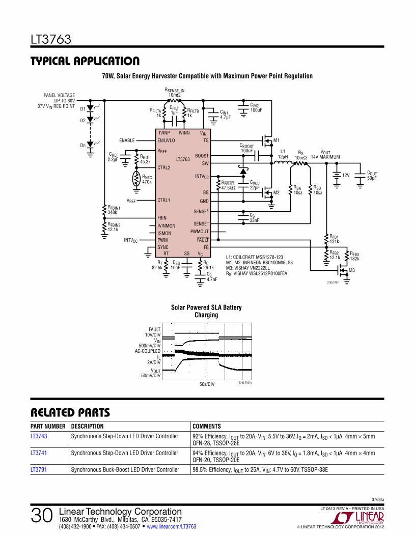
70W, Solar Energy Harvester Compatible with Maximum Power Point Regulation
RFB3182k
M3
ENABLE
CIN2100µF
PANEL VOLTAGEUP TO 60V
37V VIN REG POINT
RSENSE_IN10mΩ
RFILTA1k
RFILTB1k
RT82.5k
EN/UVLO
FBIN
TG
VINIVINNIVINP
BOOSTVREF
CTRL1VREF
CTRL2
LT3763
IVINMON
ISMON
SW
BG
GND
VC
SENSE+
SENSE–
INTVCC
INTVCC
CBOOST100nF L1
12µH
CVCC22µF
RS10mΩ
FB
FAULT
RC26.1k
CC4.7nF
RFB1121k
L1: COILCRAFT MSS1278-123M1, M2: INFINEON BSC100N06LS3M3: VISHAY VN2222LLRS: VISHAY WSL2512R0100FEA
3763 TA07
RFB212.1k
CREF2.2µF
RNTC470k
M1
M2
PWMOUT
VOUT14V MAXIMUM
12V
PWMSYNC
SS
CSS10nF
RT
RHOT45.3k
CS33nF
RSA10Ω
RSB10Ω
COUT50µF
RFAULT47.5kΩ
CFILT1µF
RFBIN1348k
RFBIN212.1k
D1
D2
Dn
CIN14.7µF
Solar Powered SLA Battery Charging
FAULT10V/DIV
VIN500mV/DIV
AC-COUPLED
VOUT50mV/DIV
IL2A/DIV
50s/DIV 3763 TA07b
LT 0513 REV A • PRINTED IN USA
LINEAR TECHNOLOGY CORPORATION 2012
Linear Technology Corporation1630 McCarthy Blvd., Milpitas, CA 95035-7417(408) 432-1900 ● FAX: (408) 434-0507 ● www.linear.com/LT3763