µC/OS-II, The Real-Time Kernels and the ARM7 / ARM9 Jean J. Labrosse
1. Introduction
1.1 About this documentThis document lists detailed information about the LPC2917/19 device. It focuses onfactual information like pinning, characteristics etc. Short descriptions are used to outlinethe concept of the features and functions. More details and background on developingapplications for this device are given in the LPC2917/19 User manual (see Ref. 1). Noexplicit references are made to the User manual.
1.2 Intended audienceThis document is written for engineers evaluating and/or developing systems, hard- and/orsoftware for the LPC2917/19. Some basic knowledge of ARM processors and architectureand ARM968E-S in particular is assumed (see Ref. 2).
2. General description
2.1 Architectural overviewThe LPC2917/19 consists of:
• An ARM968E-S processor with real-time emulation support
• An AMBA Advanced High-performance Bus (AHB) for interfacing to the on-chipmemory controllers
• Two DTL buses (a universal NXP interface) for interfacing to the interrupt controllerand the Power, Clock and Reset Control cluster (also called subsystem)
• Three ARM Peripheral Buses (APB - a compatible superset of ARM's AMBAadvanced peripheral bus) for connection to on-chip peripherals clustered insubsystems.
• One ARM Peripheral Bus for event router and system control.
The LPC2917/19 configures the ARM968E-S processor in little-endian byte order. Allperipherals run at their own clock frequency to optimize the total system powerconsumption. The AHB2APB bridge used in the subsystems contains a write-ahead bufferone transaction deep. This implies that when the ARM968E-S issues a buffered writeaction to a register located on the APB side of the bridge, it continues even though theactual write may not yet have taken place. Completion of a second write to the samesubsystem will not be executed until the first write is finished.
LPC2917/19ARM9 microcontroller with CAN and LINRev. 01 — 31 July 2008 Product data sheet
NXP Semiconductors LPC2917/19ARM9 microcontroller with CAN and LIN
2.2 ARM968E-S processorThe ARM968E-S is a general purpose 32-bit RISC processor, which offers highperformance and very low power consumption. The ARM architecture is based on RISCprinciples, and the instruction set and related decode mechanism are much simpler thanthose of microprogrammed CISC. This simplicity results in a high instruction throughputand impressive real-time interrupt response from a small and cost-effective controllercore.
Amongst the most compelling features of the ARM968E-S are:
• Separate directly connected instruction and data Tightly Coupled Memory (TCM)interfaces
• Write buffers for the AHB and TCM buses
• Enhanced 16 × 32 multiplier capable of single-cycle MAC operations and 16-bit fixed-point DSP instructions to accelerate signal-processing algorithms and applications.
Pipeline techniques are employed so that all parts of the processing and memory systemscan operate continuously. The ARM968E-S is based on the ARMv5TE five-stage pipelinearchitecture. Typically, in a three-stage pipeline architecture, while one instruction is beingexecuted its successor is being decoded and a third instruction is being fetched frommemory. In the five-stage pipeline additional stages are added for memory access andwrite-back cycles.
The ARM968E-S processor also employs a unique architectural strategy known asThumb, which makes it ideally suited to high-volume applications with memory restrictionsor to applications where code density is an issue.
The key idea behind Thumb is that of a super-reduced instruction set. Essentially, theARM968E-S processor has two instruction sets:
• Standard 32-bit ARMv5TE set
• 16-bit Thumb set
The Thumb set's 16-bit instruction length allows it to approach twice the density ofstandard ARM code while retaining most of the ARM's performance advantage over atraditional 16-bit controller using 16-bit registers. This is possible because Thumb codeoperates on the same 32-bit register set as ARM code.
Thumb code can provide up to 65 % of the code size of ARM, and 160 % of theperformance of an equivalent ARM controller connected to a 16-bit memory system.
The ARM968E-S processor is described in detail in the ARM968E-S data sheet Ref. 2.
2.3 On-chip flash memory systemThe LPC2917/19 includes a 512 kB or 768 kB flash memory system. This memory can beused for both code and data storage. Programming of the flash memory can beaccomplished in several ways. It may be programmed in-system via a serial port (e.g.,CAN).
LPC2917_19_1 © NXP B.V. 2008. All rights reserved.
Product data sheet Rev. 01 — 31 July 2008 2 of 67
NXP Semiconductors LPC2917/19ARM9 microcontroller with CAN and LIN
2.4 On-chip static RAMIn addition to the two 16 kB TCMs the LPC2917/19 includes two static RAM memories:one of 32 kB and one of 16 kB. Both may be used for code and/or data storage.
3. Features
3.1 Generaln ARM968E-S processor at 80 MHz maximum.
n AHB system bus at 80 MHz.
n On-chip memory:
u Two Tightly Coupled Memories (TCM), 16 kB Instruction TCM (ITCM), 16 kB DataTCM (DTCM).
u Two separate internal SRAM instances; 32 kB and 16 kB.
u Up to 768 kB flash program memory.
n Two-channel CAN controller supporting Full-CAN and extensive message filtering.
n Two LIN master controllers with full hardware support for LIN communication.
n Two 550 UARTs with 16-byte TX and RX FIFO depths.
n Three full-duplex queued SPIs with four slave-select lines; 16 bits wide; 8 locationsdeep; TX FIFO and RX FIFO.
n Four 32-bit timers each containing four capture-and-compare registers linked to I/Os.
n Four 6-channel PWMs with capture and trap functionality.
n 32-bit watchdog with timer change protection, running on safe clock.
n Up to 108 general-purpose I/O pins with programmable pull-up, pull-down or buskeeper.
n Vectored Interrupt Controller (VIC) with 16 priority levels.
n Two 8-channel 10-bit ADCs provide a total of up to 16 analog inputs, with conversiontimes as low as 2.44 µs per channel. Each channel provides a compare function tominimize interrupts.
n Up to 24 level-sensitive external interrupt pins, including CAN and LIN wake-upfeatures.
n External Static Memory Controller (SMC) with eight memory banks; up to 32-bit databus; up to 24-bit address bus.
n Processor wake-up from power-down via external interrupt pins; CAN or LIN activity.
n Flexible Reset Generation Unit (RGU) able to control resets of individual modules.
n Flexible Clock Generation Unit (CGU) able to control clock frequency of individualmodules:
u On-chip very low-power ring oscillator; fixed frequency of 0.4 MHz; always on toprovide a Safe_Clock source for system monitoring.
u On-chip crystal oscillator with a recommended operating range from 10 MHz to25 MHz - maximum PLL input 15 MHz.
u On-chip PLL allows CPU operation up to a maximum CPU rate of 80 MHz.
u Generation of up to 10 base clocks.
u Seven fractional dividers.
n Highly configurable system Power Management Unit (PMU):
u Clock control of individual modules.
LPC2917_19_1 © NXP B.V. 2008. All rights reserved.
Product data sheet Rev. 01 — 31 July 2008 3 of 67
NXP Semiconductors LPC2917/19ARM9 microcontroller with CAN and LIN
u Allows minimization of system operating power consumption in any configuration.
n Standard ARM test and debug interface with real-time in-circuit emulator.
n Boundary-scan test supported.
n Dual power supply:
u CPU operating voltage: 1.8 V ± 5 %.
u I/O operating voltage: 2.7 V to 3.6 V; inputs tolerant up to 5.5 V.
n 144-pin LQFP package.
n −40 °C to 85 °C ambient operating temperature range.
4. Ordering information
4.1 Ordering options
Table 1. Ordering information
Type number Package
Name Description Version
LPC2917FBD144 LQFP144 plastic low profile quad flat package; 144 leads; body 20 × 20 × 1.4 mm SOT486-1
LPC2919FBD144 LQFP144 plastic low profile quad flat package; 144 leads; body 20 × 20 × 1.4 mm SOT486-1
Table 2. Part options
Type number Flash memory RAM SMC LIN 2.0 Package
LPC2917FBD144 512 kB 80 kB (including TCMs) 32-bit 2 LQFP144
LPC2919FBD144 768 kB 80 kB (including TCMs) 32-bit 2 LQFP144
LPC2917_19_1 © NXP B.V. 2008. All rights reserved.
Product data sheet Rev. 01 — 31 July 2008 4 of 67

NXP Semiconductors LPC2917/19ARM9 microcontroller with CAN and LIN
5. Block diagram
Fig 1. LPC2917/19 block diagram
002aad840
ARM968E-S
DTCM16 kB
ITCM16 kB
TEST/DEBUGINTERFACE
EXTERNAL STATICMEMORY CONTROLLER
EMBEDDED FLASH 512/768 kB
EMBEDDED SRAM 32 kB
SYSTEM CONTROL
TIMER0/1 MTMR
CAN0/1
GLOBALACCEPTANCE
FILTER
LIN0/1
PWM0/1/2/3
ADC1/2
EVENT ROUTER
EMBEDDED SRAM 16 kB
GENERAL PURPOSE I/OPORTS 0/1/2/3
TIMER 0/1/2/3
SPI0/1/2
UART0/1
WDT
AHB TO APBBRIDGE
AHB TO DTLBRIDGE
VECTOREDINTERRUPT
CONTROLLER
AHB TO DTLBRIDGE
AHB TO APBBRIDGE
AHB TO APBBRIDGE
AHB TO APBBRIDGE
CLOCK GENERATION
UNIT
POWER MANAGEMENT
UNIT
RESET GENERATION
UNIT
LPC2917/2919
JTAGinterface
AHB bus
LPC2917_19_1 © NXP B.V. 2008. All rights reserved.
Product data sheet Rev. 01 — 31 July 2008 5 of 67
NXP Semiconductors LPC2917/19ARM9 microcontroller with CAN and LIN
6. Pinning information
6.1 Pinning
6.2 Pin description
6.2.1 General description
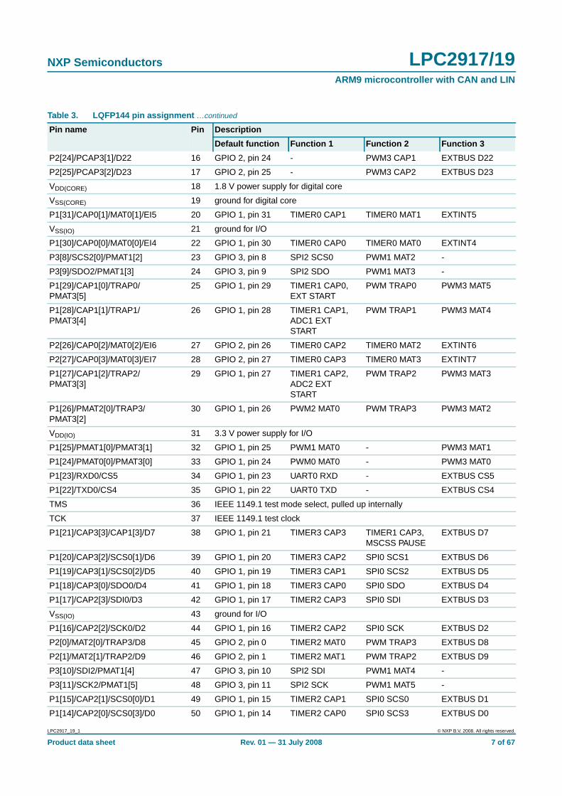
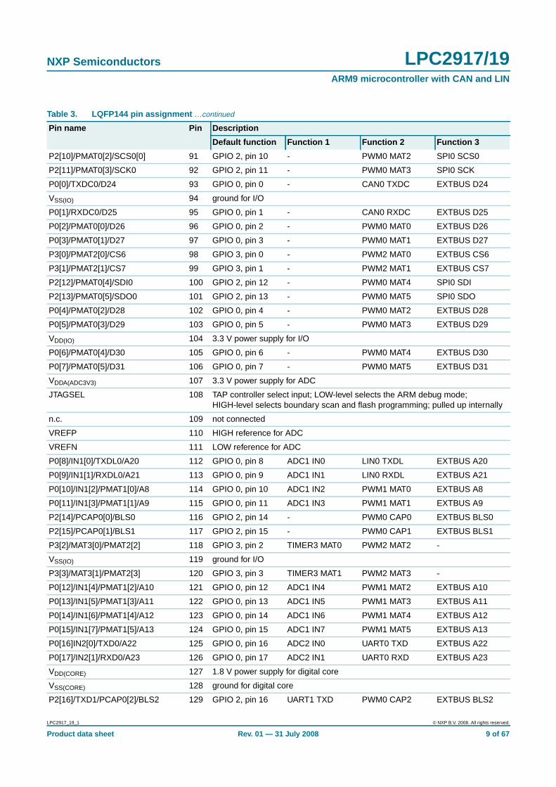
The LPC2917/19 has up to four ports: two of 32 pins each, one of 28 pins and one of 16pins. The pin to which each function is assigned is controlled by the SFSP registers in theSCU. The functions combined on each port pin are shown in the pin description tables inthis section.
6.2.2 LQFP144 pin assignment
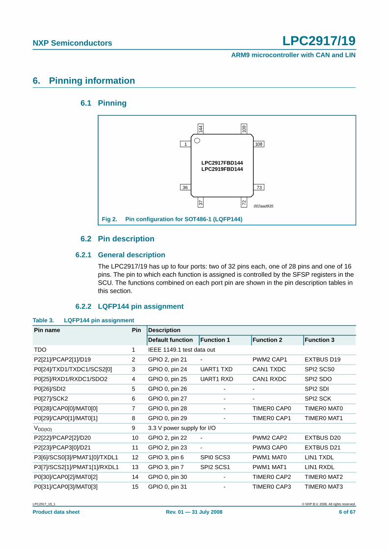
Fig 2. Pin configuration for SOT486-1 (LQFP144)
LPC2917FBD144LPC2919FBD144
108
37 72
144
109
73
1
36
002aad935
Table 3. LQFP144 pin assignment
Pin name Pin Description
Default function Function 1 Function 2 Function 3
TDO 1 IEEE 1149.1 test data out
P2[21]/PCAP2[1]/D19 2 GPIO 2, pin 21 - PWM2 CAP1 EXTBUS D19
P0[24]/TXD1/TXDC1/SCS2[0] 3 GPIO 0, pin 24 UART1 TXD CAN1 TXDC SPI2 SCS0
P0[25]/RXD1/RXDC1/SDO2 4 GPIO 0, pin 25 UART1 RXD CAN1 RXDC SPI2 SDO
P0[26]/SDI2 5 GPIO 0, pin 26 - - SPI2 SDI
P0[27]/SCK2 6 GPIO 0, pin 27 - - SPI2 SCK
P0[28]/CAP0[0]/MAT0[0] 7 GPIO 0, pin 28 - TIMER0 CAP0 TIMER0 MAT0
P0[29]/CAP0[1]/MAT0[1] 8 GPIO 0, pin 29 - TIMER0 CAP1 TIMER0 MAT1
VDD(IO) 9 3.3 V power supply for I/O
P2[22]/PCAP2[2]/D20 10 GPIO 2, pin 22 - PWM2 CAP2 EXTBUS D20
P2[23]/PCAP3[0]/D21 11 GPIO 2, pin 23 - PWM3 CAP0 EXTBUS D21
P3[6]/SCS0[3]/PMAT1[0]/TXDL1 12 GPIO 3, pin 6 SPI0 SCS3 PWM1 MAT0 LIN1 TXDL
P3[7]/SCS2[1]/PMAT1[1]/RXDL1 13 GPIO 3, pin 7 SPI2 SCS1 PWM1 MAT1 LIN1 RXDL
P0[30]/CAP0[2]/MAT0[2] 14 GPIO 0, pin 30 - TIMER0 CAP2 TIMER0 MAT2
P0[31]/CAP0[3]/MAT0[3] 15 GPIO 0, pin 31 - TIMER0 CAP3 TIMER0 MAT3
LPC2917_19_1 © NXP B.V. 2008. All rights reserved.
Product data sheet Rev. 01 — 31 July 2008 6 of 67
NXP Semiconductors LPC2917/19ARM9 microcontroller with CAN and LIN
P2[24]/PCAP3[1]/D22 16 GPIO 2, pin 24 - PWM3 CAP1 EXTBUS D22
P2[25]/PCAP3[2]/D23 17 GPIO 2, pin 25 - PWM3 CAP2 EXTBUS D23
VDD(CORE) 18 1.8 V power supply for digital core
VSS(CORE) 19 ground for digital core
P1[31]/CAP0[1]/MAT0[1]/EI5 20 GPIO 1, pin 31 TIMER0 CAP1 TIMER0 MAT1 EXTINT5
VSS(IO) 21 ground for I/O
P1[30]/CAP0[0]/MAT0[0]/EI4 22 GPIO 1, pin 30 TIMER0 CAP0 TIMER0 MAT0 EXTINT4
P3[8]/SCS2[0]/PMAT1[2] 23 GPIO 3, pin 8 SPI2 SCS0 PWM1 MAT2 -
P3[9]/SDO2/PMAT1[3] 24 GPIO 3, pin 9 SPI2 SDO PWM1 MAT3 -
P1[29]/CAP1[0]/TRAP0/PMAT3[5]
25 GPIO 1, pin 29 TIMER1 CAP0,EXT START
PWM TRAP0 PWM3 MAT5
P1[28]/CAP1[1]/TRAP1/PMAT3[4]
26 GPIO 1, pin 28 TIMER1 CAP1,ADC1 EXTSTART
PWM TRAP1 PWM3 MAT4
P2[26]/CAP0[2]/MAT0[2]/EI6 27 GPIO 2, pin 26 TIMER0 CAP2 TIMER0 MAT2 EXTINT6
P2[27]/CAP0[3]/MAT0[3]/EI7 28 GPIO 2, pin 27 TIMER0 CAP3 TIMER0 MAT3 EXTINT7
P1[27]/CAP1[2]/TRAP2/PMAT3[3]
29 GPIO 1, pin 27 TIMER1 CAP2,ADC2 EXTSTART
PWM TRAP2 PWM3 MAT3
P1[26]/PMAT2[0]/TRAP3/PMAT3[2]
30 GPIO 1, pin 26 PWM2 MAT0 PWM TRAP3 PWM3 MAT2
VDD(IO) 31 3.3 V power supply for I/O
P1[25]/PMAT1[0]/PMAT3[1] 32 GPIO 1, pin 25 PWM1 MAT0 - PWM3 MAT1
P1[24]/PMAT0[0]/PMAT3[0] 33 GPIO 1, pin 24 PWM0 MAT0 - PWM3 MAT0
P1[23]/RXD0/CS5 34 GPIO 1, pin 23 UART0 RXD - EXTBUS CS5
P1[22]/TXD0/CS4 35 GPIO 1, pin 22 UART0 TXD - EXTBUS CS4
TMS 36 IEEE 1149.1 test mode select, pulled up internally
TCK 37 IEEE 1149.1 test clock
P1[21]/CAP3[3]/CAP1[3]/D7 38 GPIO 1, pin 21 TIMER3 CAP3 TIMER1 CAP3,MSCSS PAUSE
EXTBUS D7
P1[20]/CAP3[2]/SCS0[1]/D6 39 GPIO 1, pin 20 TIMER3 CAP2 SPI0 SCS1 EXTBUS D6
P1[19]/CAP3[1]/SCS0[2]/D5 40 GPIO 1, pin 19 TIMER3 CAP1 SPI0 SCS2 EXTBUS D5
P1[18]/CAP3[0]/SDO0/D4 41 GPIO 1, pin 18 TIMER3 CAP0 SPI0 SDO EXTBUS D4
P1[17]/CAP2[3]/SDI0/D3 42 GPIO 1, pin 17 TIMER2 CAP3 SPI0 SDI EXTBUS D3
VSS(IO) 43 ground for I/O
P1[16]/CAP2[2]/SCK0/D2 44 GPIO 1, pin 16 TIMER2 CAP2 SPI0 SCK EXTBUS D2
P2[0]/MAT2[0]/TRAP3/D8 45 GPIO 2, pin 0 TIMER2 MAT0 PWM TRAP3 EXTBUS D8
P2[1]/MAT2[1]/TRAP2/D9 46 GPIO 2, pin 1 TIMER2 MAT1 PWM TRAP2 EXTBUS D9
P3[10]/SDI2/PMAT1[4] 47 GPIO 3, pin 10 SPI2 SDI PWM1 MAT4 -
P3[11]/SCK2/PMAT1[5] 48 GPIO 3, pin 11 SPI2 SCK PWM1 MAT5 -
P1[15]/CAP2[1]/SCS0[0]/D1 49 GPIO 1, pin 15 TIMER2 CAP1 SPI0 SCS0 EXTBUS D1
P1[14]/CAP2[0]/SCS0[3]/D0 50 GPIO 1, pin 14 TIMER2 CAP0 SPI0 SCS3 EXTBUS D0
Table 3. LQFP144 pin assignment …continued
Pin name Pin Description
Default function Function 1 Function 2 Function 3
LPC2917_19_1 © NXP B.V. 2008. All rights reserved.
Product data sheet Rev. 01 — 31 July 2008 7 of 67

NXP Semiconductors LPC2917/19ARM9 microcontroller with CAN and LIN
P1[13]/EI3/WE_N 51 GPIO 1, pin 13 EXTINT3 - EXTBUS WE_N
P1[12]/EI2/OE_N 52 GPIO 1, pin 12 EXTINT2 - EXTBUS OE_N
VDD(IO) 53 3.3 V power supply for I/O
P2[2]/MAT2[2]/TRAP1/D10 54 GPIO 2, pin 2 TIMER2 MAT2 PWM TRAP1 EXTBUS D10
P2[3]/MAT2[3]/TRAP0/D11 55 GPIO 2, pin 3 TIMER2 MAT3 PWM TRAP0 EXTBUS D11
P1[11]/SCK1/CS3 56 GPIO 1, pin 11 SPI1 SCK - EXTBUS CS3
P1[10]/SDI1/CS2 57 GPIO 1, pin 10 SPI1 SDI - EXTBUS CS2
P3[12]/SCS1[0]/EI4 58 GPIO 3, pin 12 SPI1 SCS0 EXTINT4 -
VSS(CORE) 59 ground for digital core
VDD(CORE) 60 1.8 V power supply for digital core
P3[13]/SDO1/EI5 61 GPIO 3, pin 13 SPI1 SDO EXTINT5 -
P2[4]/MAT1[0]/EI0/D12 62 GPIO 2, pin 4 TIMER1 MAT0 EXTINT0 EXTBUS D12
P2[5]/MAT1[1]/EI1/D13 63 GPIO 2, pin 5 TIMER1 MAT1 EXTINT1 EXTBUS D13
P1[9]/SDO1/RXDL1/CS1 64 GPIO 1, pin 9 SPI1 SDO LIN1 RXDL EXTBUS CS1
VSS(IO) 65 ground for I/O
P1[8]/SCS1[0]/TXDL1/CS0 66 GPIO 1, pin 8 SPI1 SCS0 LIN1 TXDL EXTBUS CS0
P1[7]/SCS1[3]/RXD1/A7 67 GPIO 1, pin 7 SPI1 SCS3 UART1 RXD EXTBUS A7
P1[6]/SCS1[2]/TXD1/A6 68 GPIO 1, pin 6 SPI1 SCS2 UART1 TXD EXTBUS A6
P2[6]/MAT1[2]/EI2/D14 69 GPIO 2, pin 6 TIMER1 MAT2 EXTINT2 EXTBUS D14
P1[5]/SCS1[1]/PMAT3[5]/A5 70 GPIO 1, pin 5 SPI1 SCS1 PWM3 MAT5 EXTBUS A5
P1[4]/SCS2[2]/PMAT3[4]/A4 71 GPIO 1, pin 4 SPI2 SCS2 PWM3 MAT4 EXTBUS A4
TRST_N 72 IEEE 1149.1 test reset NOT; active LOW; pulled up internally
RST_N 73 asynchronous device reset; active LOW; pulled up internally
VSS(OSC) 74 ground for oscillator
XOUT_OSC 75 crystal out for oscillator
XIN_OSC 76 crystal in for oscillator
VDD(OSC) 77 1.8 V supply for oscillator
VSS(PLL) 78 ground for PLL
P2[7]/MAT1[3]/EI3/D15 79 GPIO 2, pin 7 TIMER1 MAT3 EXTINT3 EXTBUS D15
P3[14]/SDI1/EI6/TXDC0 80 GPIO 3, pin 14 SPI1 SDI EXTINT6 CAN0 TXDC
P3[15]/SCK1/EI7/RXDC0 81 GPIO 3, pin 15 SPI1 SCK EXTINT7 CAN0 RXDC
VDD(IO) 82 3.3 V power supply for I/O
P2[8]/PMAT0[0]/SCS0[2] 83 GPIO 2, pin 8 - PWM0 MAT0 SPI0 SCS2
P2[9]/PMAT0[1]/SCS0[1] 84 GPIO 2, pin 9 - PWM0 MAT1 SPI0 SCS1
P1[3]/SCS2[1]/PMAT3[3]/A3 85 GPIO 1, pin 3 SPI2 SCS1 PWM3 MAT3 EXTBUS A3
P1[2]/SCS2[3]/PMAT3[2]/A2 86 GPIO 1, pin 2 SPI2 SCS3 PWM3 MAT2 EXTBUS A2
P1[1]/EI1/PMAT3[1]/A1 87 GPIO 1, pin 1 EXTINT1 PWM3 MAT1 EXTBUS A1
VSS(CORE) 88 ground for digital core
VDD(CORE) 89 1.8 V power supply for digital core
P1[0]/EI0/PMAT3[0]/A0 90 GPIO 1, pin 0 EXTINT0 PWM3 MAT0 EXTBUS A0
Table 3. LQFP144 pin assignment …continued
Pin name Pin Description
Default function Function 1 Function 2 Function 3
LPC2917_19_1 © NXP B.V. 2008. All rights reserved.
Product data sheet Rev. 01 — 31 July 2008 8 of 67
NXP Semiconductors LPC2917/19ARM9 microcontroller with CAN and LIN
P2[10]/PMAT0[2]/SCS0[0] 91 GPIO 2, pin 10 - PWM0 MAT2 SPI0 SCS0
P2[11]/PMAT0[3]/SCK0 92 GPIO 2, pin 11 - PWM0 MAT3 SPI0 SCK
P0[0]/TXDC0/D24 93 GPIO 0, pin 0 - CAN0 TXDC EXTBUS D24
VSS(IO) 94 ground for I/O
P0[1]/RXDC0/D25 95 GPIO 0, pin 1 - CAN0 RXDC EXTBUS D25
P0[2]/PMAT0[0]/D26 96 GPIO 0, pin 2 - PWM0 MAT0 EXTBUS D26
P0[3]/PMAT0[1]/D27 97 GPIO 0, pin 3 - PWM0 MAT1 EXTBUS D27
P3[0]/PMAT2[0]/CS6 98 GPIO 3, pin 0 - PWM2 MAT0 EXTBUS CS6
P3[1]/PMAT2[1]/CS7 99 GPIO 3, pin 1 - PWM2 MAT1 EXTBUS CS7
P2[12]/PMAT0[4]/SDI0 100 GPIO 2, pin 12 - PWM0 MAT4 SPI0 SDI
P2[13]/PMAT0[5]/SDO0 101 GPIO 2, pin 13 - PWM0 MAT5 SPI0 SDO
P0[4]/PMAT0[2]/D28 102 GPIO 0, pin 4 - PWM0 MAT2 EXTBUS D28
P0[5]/PMAT0[3]/D29 103 GPIO 0, pin 5 - PWM0 MAT3 EXTBUS D29
VDD(IO) 104 3.3 V power supply for I/O
P0[6]/PMAT0[4]/D30 105 GPIO 0, pin 6 - PWM0 MAT4 EXTBUS D30
P0[7]/PMAT0[5]/D31 106 GPIO 0, pin 7 - PWM0 MAT5 EXTBUS D31
VDDA(ADC3V3) 107 3.3 V power supply for ADC
JTAGSEL 108 TAP controller select input; LOW-level selects the ARM debug mode;HIGH-level selects boundary scan and flash programming; pulled up internally
n.c. 109 not connected
VREFP 110 HIGH reference for ADC
VREFN 111 LOW reference for ADC
P0[8]/IN1[0]/TXDL0/A20 112 GPIO 0, pin 8 ADC1 IN0 LIN0 TXDL EXTBUS A20
P0[9]/IN1[1]/RXDL0/A21 113 GPIO 0, pin 9 ADC1 IN1 LIN0 RXDL EXTBUS A21
P0[10]/IN1[2]/PMAT1[0]/A8 114 GPIO 0, pin 10 ADC1 IN2 PWM1 MAT0 EXTBUS A8
P0[11]/IN1[3]/PMAT1[1]/A9 115 GPIO 0, pin 11 ADC1 IN3 PWM1 MAT1 EXTBUS A9
P2[14]/PCAP0[0]/BLS0 116 GPIO 2, pin 14 - PWM0 CAP0 EXTBUS BLS0
P2[15]/PCAP0[1]/BLS1 117 GPIO 2, pin 15 - PWM0 CAP1 EXTBUS BLS1
P3[2]/MAT3[0]/PMAT2[2] 118 GPIO 3, pin 2 TIMER3 MAT0 PWM2 MAT2 -
VSS(IO) 119 ground for I/O
P3[3]/MAT3[1]/PMAT2[3] 120 GPIO 3, pin 3 TIMER3 MAT1 PWM2 MAT3 -
P0[12]/IN1[4]/PMAT1[2]/A10 121 GPIO 0, pin 12 ADC1 IN4 PWM1 MAT2 EXTBUS A10
P0[13]/IN1[5]/PMAT1[3]/A11 122 GPIO 0, pin 13 ADC1 IN5 PWM1 MAT3 EXTBUS A11
P0[14]/IN1[6]/PMAT1[4]/A12 123 GPIO 0, pin 14 ADC1 IN6 PWM1 MAT4 EXTBUS A12
P0[15]/IN1[7]/PMAT1[5]/A13 124 GPIO 0, pin 15 ADC1 IN7 PWM1 MAT5 EXTBUS A13
P0[16]IN2[0]/TXD0/A22 125 GPIO 0, pin 16 ADC2 IN0 UART0 TXD EXTBUS A22
P0[17]/IN2[1]/RXD0/A23 126 GPIO 0, pin 17 ADC2 IN1 UART0 RXD EXTBUS A23
VDD(CORE) 127 1.8 V power supply for digital core
VSS(CORE) 128 ground for digital core
P2[16]/TXD1/PCAP0[2]/BLS2 129 GPIO 2, pin 16 UART1 TXD PWM0 CAP2 EXTBUS BLS2
Table 3. LQFP144 pin assignment …continued
Pin name Pin Description
Default function Function 1 Function 2 Function 3
LPC2917_19_1 © NXP B.V. 2008. All rights reserved.
Product data sheet Rev. 01 — 31 July 2008 9 of 67

NXP Semiconductors LPC2917/19ARM9 microcontroller with CAN and LIN
7. Functional description
7.1 Reset, debug, test and power description
7.1.1 Reset and power-up behavior
The LPC2917/19 contains external reset input and internal power-up reset circuits. Thisensures that a reset is extended internally until the oscillators and flash have reached astable state. See Section 11 for trip levels of the internal power-up reset circuit1. SeeSection 12 for characteristics of the several start-up and initialization times. Table 4 showsthe reset pin.
At activation of the RST_N pin the JTAGSEL pin is sensed as logic LOW. If this is the casethe LPC2917/19 is assumed to be connected to debug hardware, and internal circuitsreprogram the source for the BASE_SYS_CLK to be the crystal oscillator instead of theLow-Power Ring Oscillator (LP_OSC). This is required because the clock rate whenrunning at LP_OSC speed is too low for the external debugging environment.
7.1.2 Reset strategy
The LPC2917/19 contains a central module, the Reset Generation Unit (RGU) in thePower, Clock and Reset SubSystem (PCRSS), which controls all internal reset signalstowards the peripheral modules. The RGU provides individual reset control as well as themonitoring functions needed for tracing a reset back to source.
P2[17]/RXD1/PCAP1[0]/BLS3 130 GPIO 2, pin 17 UART1 RXD PWM1 CAP0 EXTBUS BLS3
VDD(IO) 131 3.3 V power supply for I/O
P0[18]/IN2[2]/PMAT2[0]/A14 132 GPIO 0, pin 18 ADC2 IN2 PWM2 MAT0 EXTBUS A14
P0[19]/IN2[3]/PMAT2[1]/A15 133 GPIO 0, pin 19 ADC2 IN3 PWM2 MAT1 EXTBUS A15
P3[4]/MAT3[2]/PMAT2[4]/TXDC1 134 GPIO 3, pin 4 TIMER3 MAT2 PWM2 MAT4 CAN1 TXDC
P3[5]/MAT3[3]/PMAT2[5]/RXDC1 135 GPIO 3, pin 5 TIMER3 MAT3 PWM2 MAT5 CAN1 RXDC
P2[18]/PCAP1[1]/D16 136 GPIO 2, pin 18 - PWM1 CAP1 EXTBUS D16
P2[19]/PCAP1[2]/D17 137 GPIO 2, pin 19 - PWM1 CAP2 EXTBUS D17
P0[20]/IN2[4]/PMAT2[2]/A16 138 GPIO 0, pin 20 ADC2 IN4 PWM2 MAT2 EXTBUS A16
P0[21]/IN2[5]/PMAT2[3]/A17 139 GPIO 0, pin 21 ADC2 IN5 PWM2 MAT3 EXTBUS A17
P0[22]/IN2[6]/PMAT2[4]/A18 140 GPIO 0, pin 22 ADC2 IN6 PWM2 MAT4 EXTBUS A18
VSS(IO) 141 ground for I/O
P0[23]/IN2[7]/PMAT2[5]/A19 142 GPIO 0, pin 23 ADC2 IN7 PWM2 MAT5 EXTBUS A19
P2[20]/PCAP2[0]/D18 143 GPIO 2, pin 20 - PWM2 CAP0 EXTBUS D18
TDI 144 IEEE 1149.1 data in, pulled up internally
Table 3. LQFP144 pin assignment …continued
Pin name Pin Description
Default function Function 1 Function 2 Function 3
1. Only for 1.8 V power sources
Table 4. Reset pin
Symbol Direction Description
RST_N IN external reset input, active LOW; pulled up internally
LPC2917_19_1 © NXP B.V. 2008. All rights reserved.
Product data sheet Rev. 01 — 31 July 2008 10 of 67

NXP Semiconductors LPC2917/19ARM9 microcontroller with CAN and LIN
7.1.3 IEEE 1149.1 interface pins (JTAG boundary-scan test)
The LPC2917/19 contains boundary-scan test logic according to IEEE 1149.1, alsoreferred to in this document as JTAG. The boundary-scan test pins can be used toconnect a debugger probe for the embedded ARM processor. Pin JTAGSEL selectsbetween boundary-scan mode and debug mode. Table 5 shows the boundary- scan testpins.
7.1.4 Power supply pins description
Table 6 shows the power supply pins.
7.2 Clocking strategy
7.2.1 Clock architecture
The LPC2917/19 contains several different internal clock areas. Peripherals like Timers,SPI, UART, CAN and LIN have their own individual clock sources called Base Clocks. Allbase clocks are generated by the Clock Generation Unit (CGU). They may be unrelated infrequency and phase and can have different clock sources within the CGU.
The system clock for the CPU and AHB Bus infrastructure has its own base clock. Thismeans most peripherals are clocked independently from the system clock. See Figure 3for an overview of the clock areas within the device.
Within each clock area there may be multiple branch clocks, which offers very flexiblecontrol for power-management purposes. All branch clocks are outputs of the PowerManagement Unit (PMU) and can be controlled independently. Branch clocks derivedfrom the same base clock are synchronous in frequency and phase. See Section 8.8 formore details of clock and power control within the device.
Table 5. IEEE 1149.1 boundary-scan test and debug interface
Symbol Description
JTAGSEL TAP controller select input. LOW-level selects ARM debug mode and HIGH-levelselects boundary scan and flash programming; pulled up internally
TRST_N test reset input; pulled up internally (active LOW)
TMS test mode select input; pulled up internally
TDI test data input, pulled up internally
TDO test data output
TCK test clock input
Table 6. Power supplies
Symbol Description
VDD(CORE) digital core supply 1.8 V
VSS(CORE) digital core ground (digital core, ADC1/2)
VDD(IO) I/O pins supply 3.3 V
VSS(IO) I/O pins ground
VDD(OSC) oscillator and PLL supply
VSS(OSC) oscillator ground
VDDA(ADC3V3) ADC1/2 3.3 V supply
VSS(PLL) PLL ground
LPC2917_19_1 © NXP B.V. 2008. All rights reserved.
Product data sheet Rev. 01 — 31 July 2008 11 of 67

NXP Semiconductors LPC2917/19ARM9 microcontroller with CAN and LIN
7.2.2 Base clock and branch clock relationship
The next table contains an overview of all the base blocks in the LPC2917/19 and theirderived branch clocks. A short description is given of the hardware parts that are clockedwith the individual branch clocks. In relevant cases more detailed information can be
Fig 3. LPC2917/19 block diagram, overview of clock areas
002aad839
ARM968E-S
DTCM16 kB
ITCM16 kB
TEST/DEBUGINTERFACE
MEMORYSUBSYSTEM
SYSTEM CONTROL
TIMER0/1 MTMR
CAN0/1
GLOBALACCEPTANCE
FILTER
LIN0/1
PWM0/1/2/3
ADC1/2
EVENT ROUTER
GENERAL PURPOSE I/O
TIMER 0/1/2/3
SPI0/1/2
UART0/1
WDT
AHB TO APBBRIDGE
AHB TO DTLBRIDGE
VECTOREDINTERRUPT
CONTROLLER
AHB TO DTLBRIDGE
AHB TO APBBRIDGE
AHB TO APBBRIDGE
AHB TO APBBRIDGE
RESET/CLOCK GENERATION
POWERMANAGEMENT
LPC2917/2919
JTAGinterface
TMR_CLK
SPI_CLK
UART_CLK
SAFE_CLK
IVNSS_CLK
PCR_CLK
SYS_CLK
MSCSS_CLK
ADC_CLK
AHB bus
LPC2917_19_1 © NXP B.V. 2008. All rights reserved.
Product data sheet Rev. 01 — 31 July 2008 12 of 67

NXP Semiconductors LPC2917/19ARM9 microcontroller with CAN and LIN
found in the specific subsystem description. Some branch clocks have special protectionsince they clock vital system parts of the device and should (for example) not be switchedoff. See Section 8.8.6 for more details of how to control the individual branch clocks.
Table 7. Base clock and branch clock overview
Base clock Branch clock name Parts of the device clocked bythis branch clock
Remark
BASE_SAFE_CLK CLK_SAFE watchdog timer [1]
BASE_SYS_CLK CLK_SYS_CPU ARM968E-S and TCMs
CLK_SYS_SYS AHB bus infrastructure
CLK_SYS_PCRSS AHB side of bridge in PCRSS
CLK_SYS_FMC Flash Memory Controller
CLK_SYS_RAM0 Embedded SRAM Controller 0(32 kB)
CLK_SYS_RAM1 Embedded SRAM Controller 1(16 kB)
CLK_SYS_SMC External Static MemoryController
CLK_SYS_GESS General Subsystem
CLK_SYS_VIC Vectored Interrupt Controller
CLK_SYS_PESS Peripheral Subsystem [2] [4]
CLK_SYS_GPIO0 GPIO bank 0
CLK_SYS_GPIO1 GPIO bank 1
CLK_SYS_GPIO2 GPIO bank 2
CLK_SYS_GPIO3 GPIO bank 3
CLK_SYS_IVNSS_A AHB side of bridge of IVNSS
BASE_PCR_CLK CLK_PCR_SLOW PCRSS, CGU, RGU and PMUlogic clock
[1], [3]
BASE_IVNSS_CLK CLK_IVNSS_APB APB side of the IVNSS
CLK_IVNSS_CANCA CAN controller Acceptance Filter
CLK_IVNSS_CANC0 CAN channel 0
CLK_IVNSS_CANC1 CAN channel 1
CLK_IVNSS_LIN0 LIN channel 0
CLK_IVNSS_LIN1 LIN channel 1
BASE_MSCSS_CLK CLK_MSCSS_APB APB side of the MSCSS
CLK_MSCSS_MTMR0 Timer 0 in the MSCSS
CLK_MSCSS_MTMR1 Timer 1 in the MSCSS
CLK_MSCSS_PWM0 PWM 0
CLK_MSCSS_PWM1 PWM 0
CLK_MSCSS_PWM2 PWM 0
CLK_MSCSS_PWM3 PWM 0
CLK_MSCSS_ADC1_APB
APB side of ADC 1
CLK_MSCSS_ADC2_APB
APB side of ADC 2
LPC2917_19_1 © NXP B.V. 2008. All rights reserved.
Product data sheet Rev. 01 — 31 July 2008 13 of 67

NXP Semiconductors LPC2917/19ARM9 microcontroller with CAN and LIN
[1] This clock is always on (cannot be switched off for system safety reasons)
[2] In the peripheral subsystem parts of the Timers, watchdog timer, SPI and UART have their own clocksource. See Section 8.4 for details.
[3] In the Power Clock and Reset Control subsystem parts of the CGU, RGU PMU have their own clock source.See Section 8.8 for details.
[4] The clock should remain activated when system wake-up on timer or UART is required.
8. Block description
8.1 Flash memory controller
8.1.1 Overview
The Flash Memory Controller (FMC) interfaces to the embedded flash memory for twotasks:
• Providing memory data transfer
• Memory configuration via triggering, programming and erasing
The flash memory has a 128-bit wide data interface and the flash controller offers two128-bit buffer lines to improve system performance. The flash has to be programmedinitially via JTAG. In-system programming must be supported by the bootloader.In-application programming is possible. Flash memory contents can be protected bydisabling JTAG access. Suspension of burning or erasing is not supported.
The key features are:
• Programming by CPU via AHB
• Programming by external programmer via JTAG
• JTAG access protection
• Burn-finished and erase-finished interrupt
BASE_UART_CLK CLK_UART0 UART 0 interface clock
CLK_UART1 UART 1 interface clock
BASE_SPI_CLK CLK_SPI0 SPI 0 interface clock
CLK_SPI1 SPI 1 interface clock
CLK_SPI2 SPI 2 interface clock
BASE_TMR_CLK CLK_TMR0 Timer 0 clock for counter part
CLK_TMR1 Timer 1 clock for counter part
CLK_TMR2 Timer 2 clock for counter part
CLK_TMR3 Timer 3 clock for counter part
BASE_ADC_CLK CLK_ADC1 Control of ADC 1, capture sampleresult
CLK_ADC2 Control of ADC 2, capture sampleresult
BASE_CLK_TESTSHELL CLK_TESTSHELL_IP
Table 7. Base clock and branch clock overview …continued
Base clock Branch clock name Parts of the device clocked bythis branch clock
Remark
LPC2917_19_1 © NXP B.V. 2008. All rights reserved.
Product data sheet Rev. 01 — 31 July 2008 14 of 67
NXP Semiconductors LPC2917/19ARM9 microcontroller with CAN and LIN
8.1.2 Description
After reset flash initialization is started, which takes tinit time, see Section 12. During thisinitialization flash access is not possible and AHB transfers to flash are stalled, blockingthe AHB bus.
During flash initialization the index sector is read to identify the status of the JTAG accessprotection and sector security. If JTAG access protection is active the flash is notaccessible via JTAG. ARM debug facilities are disabled to protect the flash memorycontents against unwanted reading out externally. If sector security is active only theconcerned sections are read.
Flash can be read synchronously or asynchronously to the system clock. In synchronousoperation the flash goes into standby after returning the read data. Started reads cannotbe stopped, and speculative reading and dual buffering are therefore not supported.
With asynchronous reading, transfer of the address to the flash and of read data from theflash is done asynchronously, giving the fastest possible response time. Started reads canbe stopped, so speculative reading and dual buffering are supported.
Buffering is offered because the flash has a 128-bit wide data interface while the AHBinterface has only 32 bits. With buffering a buffer line holds the complete 128-bit flashword, from which four words can be read. Without buffering every AHB data port readstarts a flash read. A flash read is a slow process compared to the minimum AHB cycletime, so with buffering the average read time is reduced. This can improve systemperformance.
With single buffering the most recently read flash word remains available until the nextflash read. When an AHB data-port read transfer requires data from the same flash wordas the previous read transfer, no new flash read is done and the read data is given withoutwait cycles.
When an AHB data-port read transfer requires data from a different flash word to thatinvolved in the previous read transfer, a new flash read is done and wait states are givenuntil the new read data is available.
With dual buffering a secondary buffer line is used, the output of the flash beingconsidered as the primary buffer. On a primary buffer hit data can be copied to thesecondary buffer line, which allows the flash to start a speculative read of the next flashword.
Both buffer lines are invalidated after:
• Initialization
• Configuration-register access
• Data-latch reading
• Index-sector reading
The modes of operation are listed in Table 8.
LPC2917_19_1 © NXP B.V. 2008. All rights reserved.
Product data sheet Rev. 01 — 31 July 2008 15 of 67
NXP Semiconductors LPC2917/19ARM9 microcontroller with CAN and LIN
8.1.3 Flash memory controller pin description
The flash memory controller has no external pins. However, the flash can be programmedvia the JTAG pins, see Section 7.1.3.
8.1.4 Flash memory controller clock description
The flash memory controller is clocked by CLK_SYS_FMC, see Section 7.2.2.
8.1.5 Flash layout
The ARM processor can program the flash for ISP (In-System Programming) and IAP (In-Application Programming). Note that the flash always has to be programmed by ‘flashwords’ of 128 bits (four 32-bit AHB bus words, hence 16 bytes).
The flash memory is organized into eight ‘small’ sectors of 8 kB each and up to 11 ‘large’sectors of 64 kB each. The number of large sectors depends on the device type. A sectormust be erased before data can be written to it. The flash memory also has sector-wiseprotection. Writing occurs per page which consists of 4096 bits (32 flash words). A smallsector contains 16 pages; a large sector contains 128 pages.
Table 9 gives an overview of the flash sector base addresses.
Table 8. Flash read modes
Synchronous timing
No buffer line for single (non-linear) reads; one flash word read per word read
Single buffer line default mode of operation; most recently read flash word is kept untilanother flash word is required
Asynchronous timing
No buffer line one flash word read per word read
Single buffer line most recently read flash word is kept until another flash word isrequired
Dual buffer line, singlespeculative
on a buffer miss a flash read is done, followed by at most onespeculative read; optimized for execution of code with small loops(less than eight words) from flash
Dual buffer line, alwaysspeculative
most recently used flash word is copied into second buffer line; nextflash word read is started; highest performance for linear reads
Table 9. Flash sector overview
Sector number Sector size (kB) Sector base address
0 8 0000 0000h
1 8 0000 2000h
2 8 0000 4000h
3 8 0000 6000h
4 8 0000 8000h
5 8 0000 A000h
6 8 0000 C000h
7 8 0000 E000h
8 64 0001 0000h
9 64 0002 0000h
10 64 0003 0000h
LPC2917_19_1 © NXP B.V. 2008. All rights reserved.
Product data sheet Rev. 01 — 31 July 2008 16 of 67

NXP Semiconductors LPC2917/19ARM9 microcontroller with CAN and LIN
[1] Availability of sector 15 to sector 18 depends on device type, see Section 4 “Ordering information”.
The index sector is a special sector in which the JTAG access protection and sectorsecurity are located. The address space becomes visible by setting the FS_ISS bit andoverlaps the regular flash sector’s address space.
Note that the index sector cannot be erased, and that access to it has to be performed viacode outside the flash.
8.1.6 Flash bridge wait-states
To eliminate the delay associated with synchronizing flash read data, a predefined numberof wait-states must be programmed. These depend on flash memory response time andsystem clock period. The minimum wait-states value can be calculated with the followingformulas:
Synchronous reading:
(1)
Asynchronous reading:
(2)
Remark: If the programmed number of wait-states is more than three, flash data readingcannot be performed at full speed (i.e., with zero wait-states at the AHB bus) if speculativereading is active.
8.2 External static memory controller
8.2.1 Overview
The LPC2917/19 contains an external Static Memory Controller (SMC) which provides aninterface for external (off-chip) memory devices.
Key features are:
• Supports static memory-mapped devices including RAM, ROM, flash, burst ROM andexternal I/O devices
11 64 0004 0000h
12 64 0005 0000h
13 64 0006 0000h
14 64 0007 0000h
15[1] 64 0008 0000h
16[1] 64 0009 0000h
17[1] 64 000A 0000h
18[1] 64 000B 0000h
Table 9. Flash sector overview …continued
Sector number Sector size (kB) Sector base address
WSTtacc clk( )tttclk sys( )
------------------> 1–
WSTtacc addr( )ttclk sys( )----------------------> 1–
LPC2917_19_1 © NXP B.V. 2008. All rights reserved.
Product data sheet Rev. 01 — 31 July 2008 17 of 67
NXP Semiconductors LPC2917/19ARM9 microcontroller with CAN and LIN
• Asynchronous page-mode read operation in non-clocked memory subsystems
• Asynchronous burst-mode read access to burst-mode ROM devices
• Independent configuration for up to eight banks, each up to 16 MB
• Programmable bus-turnaround (idle) cycles (one to 16)
• Programmable read and write wait states (up to 32), for static RAM devices
• Programmable initial and subsequent burst-read wait state for burst-ROM devices
• Programmable write protection
• Programmable burst-mode operation
• Programmable external data width: 8 bits, 16 bits or 32 bits
• Programmable read-byte lane enable control
8.2.2 Description
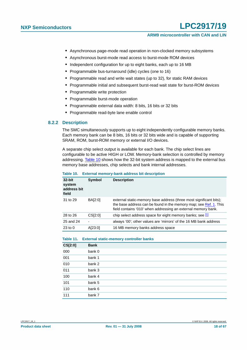
The SMC simultaneously supports up to eight independently configurable memory banks.Each memory bank can be 8 bits, 16 bits or 32 bits wide and is capable of supportingSRAM, ROM, burst-ROM memory or external I/O devices.
A separate chip select output is available for each bank. The chip select lines areconfigurable to be active HIGH or LOW. Memory-bank selection is controlled by memoryaddressing. Table 10 shows how the 32-bit system address is mapped to the external busmemory base addresses, chip selects and bank internal addresses.
Table 10. External memory-bank address bit description
32-bitsystemaddress bitfield
Symbol Description
31 to 29 BA[2:0] external static-memory base address (three most significant bits);the base address can be found in the memory map; see Ref. 1. Thisfield contains ‘010’ when addressing an external memory bank.
28 to 26 CS[2:0] chip select address space for eight memory banks; see [1]
25 and 24 - always ‘00’; other values are ‘mirrors’ of the 16 MB bank address
23 to 0 A[23:0] 16 MB memory banks address space
Table 11. External static-memory controller banks
CS[2:0] Bank
000 bank 0
001 bank 1
010 bank 2
011 bank 3
100 bank 4
101 bank 5
110 bank 6
111 bank 7
LPC2917_19_1 © NXP B.V. 2008. All rights reserved.
Product data sheet Rev. 01 — 31 July 2008 18 of 67

NXP Semiconductors LPC2917/19ARM9 microcontroller with CAN and LIN
8.2.3 External static-memory controller pin description
The external static-memory controller module in the LPC2917/19 has the following pins,which are combined with other functions on the port pins of the LPC2917/19. Table 12shows the external memory controller pins.
8.2.4 External static-memory controller clock description
The External Static-Memory Controller is clocked by CLK_SYS_SMC, see Section 7.2.2.
8.2.5 External memory timing diagrams
A timing diagram for reading from external memory is shown in Figure 4. The relationshipbetween the wait-state settings is indicated with arrows.
A timing diagram for writing to external memory is shown In Figure 5. The relationshipbetween wait-state settings is indicated with arrows.
Table 12. External memory controller pins
Symbol Direction Description
EXTBUS CSx OUT memory-bank x select, x runs from 0 to 7
EXTBUS BLSy OUT byte-lane select input y, y runs from 0 to 3
EXTBUS WE_N OUT write enable (active LOW)
EXTBUS OE_N OUT output enable (active LOW)
EXTBUS A[23:0] OUT address bus
EXTBUS D[31:0] IN/OUT data bus
WSTOEN = 3, WST1 = 7
Fig 4. Reading from external memory
OE_N
CLK(SYS)
CS
ADDR
DATA
WSTOEN
WST1 002aad936
LPC2917_19_1 © NXP B.V. 2008. All rights reserved.
Product data sheet Rev. 01 — 31 July 2008 19 of 67
NXP Semiconductors LPC2917/19ARM9 microcontroller with CAN and LIN
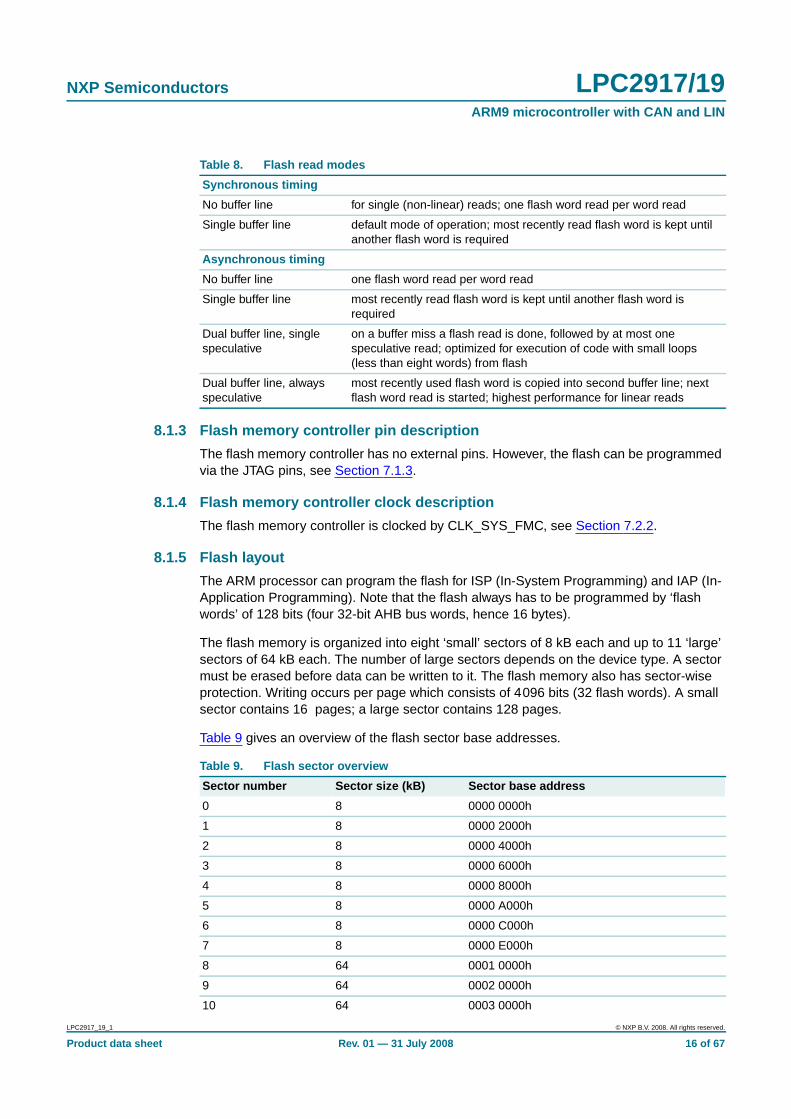
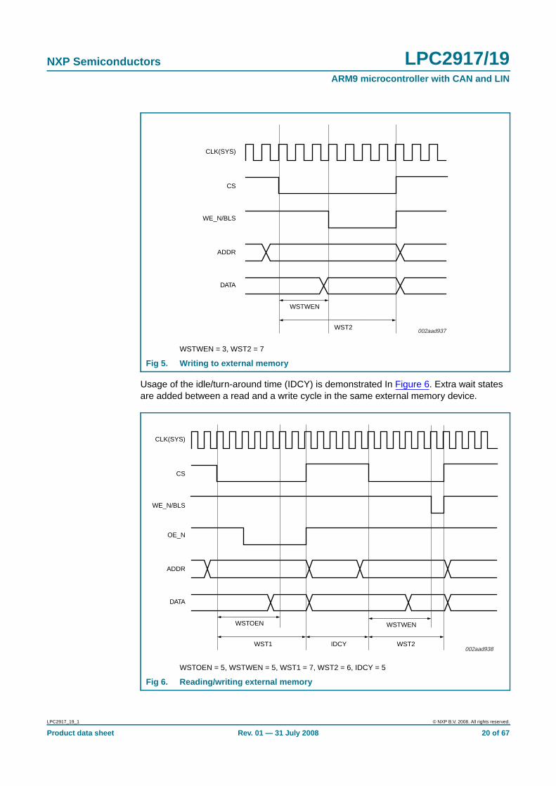
Usage of the idle/turn-around time (IDCY) is demonstrated In Figure 6. Extra wait statesare added between a read and a write cycle in the same external memory device.
WSTWEN = 3, WST2 = 7
Fig 5. Writing to external memory
WSTOEN = 5, WSTWEN = 5, WST1 = 7, WST2 = 6, IDCY = 5
Fig 6. Reading/writing external memory
WE_N/BLS
CLK(SYS)
CS
ADDR
DATA
WSTWEN
WST2 002aad937
OE_N
CLK(SYS)
CS
ADDR
DATA
WSTOEN
WST1
WSTWEN
WST2IDCY002aad938
WE_N/BLS
LPC2917_19_1 © NXP B.V. 2008. All rights reserved.
Product data sheet Rev. 01 — 31 July 2008 20 of 67
NXP Semiconductors LPC2917/19ARM9 microcontroller with CAN and LIN
Address pins on the device are shared with other functions. When connecting externalmemories, check that the I/O pin is programmed for the correct function. Control of thesesettings is handled by the SCU.
8.3 General subsystem
8.3.1 General subsystem clock description
The general subsystem is clocked by CLK_SYS_GESS, see Section 7.2.2.
8.3.2 Chip and feature identification
8.3.2.1 Overview
The key features are:
• Identification of product
• Identification of features enabled
8.3.2.2 Description
The Chip/Feature ID (CFID) module contains registers which show and control thefunctionality of the chip. It contains an ID to identify the silicon, and also registerscontaining information about the features enabled or disabled on the chip.
8.3.2.3 CFID pin description
The CFID has no external pins.
8.3.3 System control unit
8.3.3.1 Overview
The SCU takes care of system-related functions.The key feature is configuration of the I/Oport-pins multiplexer.
8.3.3.2 Description
The SCU defines the function of each I/O pin of the LPC2917/19. The I/O pinconfiguration should be consistent with peripheral function usage.
8.3.3.3 SCU pin description
The SCU has no external pins.
8.3.4 Event router
8.3.4.1 Overview
The event router provides bus-controlled routing of input events to the vectored interruptcontroller for use as interrupt or wake-up signals.
Key features:
• Up to 24 level-sensitive external interrupt pins, including CAN, LIN and RXD wake-upfeatures plus three internal event sources
• Input events can be used as interrupt source either directly or latched (edge-detected)
• Direct events disappear when the event becomes inactive
LPC2917_19_1 © NXP B.V. 2008. All rights reserved.
Product data sheet Rev. 01 — 31 July 2008 21 of 67

NXP Semiconductors LPC2917/19ARM9 microcontroller with CAN and LIN
• Latched events remain active until they are explicitly cleared
• Programmable input level and edge polarity
• Event detection maskable
• Event detection is fully asynchronous, so no clock is required
8.3.4.2 Description
The event router allows the event source to be defined, its polarity and activation type tobe selected and the interrupt to be masked or enabled. The event router can be used tostart a clock on an external event.
The vectored interrupt-controller inputs are active HIGH.
8.3.4.3 Event-router pin description and mapping to register bit positions
The event router module in the LPC2917/19 is connected to the pins listed below. Thepins are combined with other functions on the port pins of the LPC2917/19. Table 13shows the pins connected to the event router, and also the corresponding bit position inthe event-router registers and the default polarity.
8.4 Peripheral subsystem
8.4.1 Peripheral subsystem clock description
The peripheral subsystem is clocked by a number of different clocks:
• CLK_SYS_PESS
Table 13. Event-router pin connections
Symbol Direction Bit position Description Defaultpolarity
EXTINT0 IN 0 external interrupt input 0 1
EXTINT1 IN 1 external interrupt input 1 1
EXTINT2 IN 2 external interrupt input 2 1
EXTINT3 IN 3 external interrupt input 3 1
EXTINT4 IN 4 external interrupt input 4 1
EXTINT5 IN 5 external interrupt input 5 1
EXTINT6 IN 6 external interrupt input 6 1
EXTINT7 IN 7 external interrupt input 7 1
CAN0 RXDC IN 8 CAN0 receive data input wake-up 0
CAN1 RXDC IN 9 CAN1 receive data input wake-up 0
- - 13 to 10 reserved -
LIN0 RXDL IN 14 LIN0 receive data input wake-up 0
LIN1 RXDL IN 15 LIN1 receive data input wake-up 0
- - 21 to 16 reserved -
- na 22 CAN interrupt (internal) 1
- na 23 VIC FIQ (internal) 1
- na 24 VIC IRQ (internal) 1
- - 26 to 25 reserved -
LPC2917_19_1 © NXP B.V. 2008. All rights reserved.
Product data sheet Rev. 01 — 31 July 2008 22 of 67
NXP Semiconductors LPC2917/19ARM9 microcontroller with CAN and LIN
• CLK_UART0/1
• CLK_SPI0/1/2
• CLK_TMR0/1/2/3
• CLK_SAFE see Section 7.2.2
8.4.2 Watchdog timer
8.4.2.1 Overview
The purpose of the watchdog timer is to reset the ARM9 processor within a reasonableamount of time if the processor enters an error state. The watchdog generates a systemreset if the user program fails to trigger it correctly within a predetermined amount of time.
Key features:
• Internal chip reset if not periodically triggered
• Timer counter register runs on always-on safe clock
• Optional interrupt generation on watchdog time-out
• Debug mode with disabling of reset
• Watchdog control register change-protected with key
• Programmable 32-bit watchdog timer period with programmable 32-bit prescaler.
8.4.2.2 Description
The watchdog timer consists of a 32-bit counter with a 32-bit prescaler.
The watchdog should be programmed with a time-out value and then periodicallyrestarted. When the watchdog times out it generates a reset through the RGU.
To generate watchdog interrupts in watchdog debug mode the interrupt has to be enabledvia the interrupt enable register. A watchdog-overflow interrupt can be cleared by writingto the clear-interrupt register.
Another way to prevent resets during debug mode is via the Pause feature of thewatchdog timer. The watchdog is stalled when the ARM9 is in debug mode and thePAUSE_ENABLE bit in the watchdog timer control register is set.
The Watchdog Reset output is fed to the Reset Generation Unit (RGU). The RGUcontains a reset source register to identify the reset source when the device has gonethrough a reset. See Section 8.8.5.
8.4.2.3 Pin description
The watchdog has no external pins.
8.4.2.4 Watchdog timer clock description
The watchdog timer is clocked by two different clocks; CLK_SYS_PESS and CLK_SAFE,see Section 7.2.2. The register interface towards the system bus is clocked byCLK_SYS_PESS. The timer and prescale counters are clocked by CLK_SAFE which isalways on.
LPC2917_19_1 © NXP B.V. 2008. All rights reserved.
Product data sheet Rev. 01 — 31 July 2008 23 of 67

NXP Semiconductors LPC2917/19ARM9 microcontroller with CAN and LIN
8.4.3 Timer
8.4.3.1 Overview
The LPC2917/19 contains six identical timers: four in the peripheral subsystem and two inthe Modulation and Sampling Control SubSystem (MSCSS) located at different peripheralbase addresses. This section describes the four timers in the peripheral subsystem. Eachtimer has four capture inputs and/or match outputs. Connection to device pins depends onthe configuration programmed into the port function-select registers. The two timerslocated in the MSCSS have no external capture or match pins, but the memory map isidentical, see Section 8.7.7. One of these timers has an external input for a pausefunction.
The key features are:
• 32-bit timer/counter with programmable 32-bit prescaler
• Up to four 32-bit capture channels per timer. These take a snapshot of the timer valuewhen an external signal connected to the TIMERx CAPn input changes state. Acapture event may also optionally generate an interrupt
• Four 32-bit match registers per timer that allow:
– Continuous operation with optional interrupt generation on match
– Stop timer on match with optional interrupt generation
– Reset timer on match with optional interrupt generation
• Up to four external outputs per timer corresponding to match registers, with thefollowing capabilities:
– Set LOW on match
– Set HIGH on match
– Toggle on match
– Do nothing on match
• Pause input pin (MSCSS timers only)
8.4.3.2 Description
The timers are designed to count cycles of the clock and optionally generate interrupts orperform other actions at specified timer values, based on four match registers. They alsoinclude capture inputs to trap the timer value when an input signal changes state,optionally generating an interrupt. The core function of the timers consists of a 32 bit‘prescale counter’ triggering the 32 bit ‘timer counter’. Both counters run on clockCLK_TMRx (x runs from 0 to 3) and all time references are related to the period of thisclock. Note that each timer has its individual clock source within the PeripheralSubSystem. In the Modulation and Sampling SubSystem each timer also has its ownindividual clock source. See section Section 8.8.6 for information on generation of theseclocks.
8.4.3.3 Pin description
The four timers in the peripheral subsystem of the LPC2917/19 have the pins describedbelow. The two timers in the modulation and sampling subsystem have no external pinsexcept for the pause pin on MSCSS timer 1. See Section 8.7.7 for a description of these
LPC2917_19_1 © NXP B.V. 2008. All rights reserved.
Product data sheet Rev. 01 — 31 July 2008 24 of 67

NXP Semiconductors LPC2917/19ARM9 microcontroller with CAN and LIN
timers and their associated pins. The timer pins are combined with other functions on theport pins of the LPC2917/19, see Section 8.3.3. Table Table 14 shows the timer pins (xruns from 0 to 3).
8.4.3.4 Timer clock description
The timer modules are clocked by two different clocks; CLK_SYS_PESS and CLK_TMRx(x = 0-3), see Section 7.2.2. Note that each timer has its own CLK_TMRx branch clock forpower management. The frequency of all these clocks is identical as they are derived fromthe same base clock BASE_CLK_TMR. The register interface towards the system bus isclocked by CLK_SYS_PESS. The timer and prescale counters are clocked byCLK_TMRx.
8.4.4 UARTs
8.4.4.1 Overview
The LPC2917/19 contains two identical UARTs located at different peripheral baseaddresses. The key features are:
• 16-byte receive and transmit FIFOs
• Register locations conform to 550 industry standard
• Receiver FIFO trigger points at 1 byte, 4 bytes, 8 bytes and 14 bytes
• Built-in baud rate generator
8.4.4.2 Description
The UART is commonly used to implement a serial interface such as RS232. TheLPC2917/19 contains two industry-standard 550 UARTs with 16-byte transmit and receiveFIFOs, but they can also be put into 450 mode without FIFOs.
8.4.4.3 UART pin description
The two UARTs in the LPC2917/19 have the following pins. The UART pins are combinedwith other functions on the port pins of the LPC2917/19. Table 15 shows the UART pins (xruns from 0 to 1).
Table 14. Timer pins
Symbol Direction Description
TIMERx CAP[0] IN TIMER x capture input 0
TIMERx CAP[1] IN TIMER x capture input 1
TIMERx CAP[2] IN TIMER x capture input 2
TIMERx CAP[3] IN TIMER x capture input 3
TIMERx MAT[0] OUT TIMER x match output 0
TIMERx MAT[1] OUT TIMER x match output 1
TIMERx MAT[2] OUT TIMER x match output 2
TIMERx MAT[3] OUT TIMER x match output 3
Table 15. UART pins
Symbol Direction Description
UARTx TXD OUT UART channel x transmit data output
UARTx RXD IN UART channel x receive data input
LPC2917_19_1 © NXP B.V. 2008. All rights reserved.
Product data sheet Rev. 01 — 31 July 2008 25 of 67
NXP Semiconductors LPC2917/19ARM9 microcontroller with CAN and LIN
8.4.4.4 UART clock description
The UART modules are clocked by two different clocks; CLK_SYS_PESS andCLK_UARTx (x = 0-1), see Section 7.2.2. Note that each UART has its own CLK_UARTxbranch clock for power management. The frequency of all CLK_UARTx clocks is identicalsince they are derived from the same base clock BASE_CLK_UART. The registerinterface towards the system bus is clocked by CLK_SYS_PESS. The baud generator isclocked by the CLK_UARTx.
8.4.5 Serial peripheral interface
8.4.5.1 Overview
The LPC2917/19 contains three SPI modules to allow synchronous serial communicationwith slave or master peripherals.
The key features are:
• Master or slave operation
• Supports up to four slaves in sequential multi-slave operation
• Supports timer-triggered operation
• Programmable clock bit rate and prescale based on SPI source clock(BASE_SPI_CLK), independent of system clock
• Separate transmit and receive FIFO memory buffers; 16 bits wide, 32 locations deep
• Programmable choice of interface operation: Motorola SPI or Texas InstrumentsSynchronous Serial Interfaces
• Programmable data-frame size from 4 to 16 bits
• Independent masking of transmit FIFO, receive FIFO and receive overrun interrupts
• Serial clock-rate master mode: fserial_clk ≤ fCLK(SPI)*/2
• Serial clock-rate slave mode: fserial_clk = fCLK(SPI)*/4
• Internal loopback test mode
8.4.5.2 Functional description
The SPI module is a master or slave interface for synchronous serial communication withperipheral devices that have either Motorola SPI or Texas Instruments Synchronous SerialInterfaces.
The SPI module performs serial-to-parallel conversion on data received from a peripheraldevice. The transmit and receive paths are buffered with FIFO memories (16 bits wide ×32 words deep). Serial data is transmitted on SPI_TXD and received on SPI_RXD.
The SPI module includes a programmable bit-rate clock divider and prescaler to generatethe SPI serial clock from the input clock CLK_SPIx.
The SPI module’s operating mode, frame format, and word size are programmed throughthe SLVn_SETTINGS registers.
A single combined interrupt request SPI_INTREQ output is asserted if any of theinterrupts are asserted and unmasked.
LPC2917_19_1 © NXP B.V. 2008. All rights reserved.
Product data sheet Rev. 01 — 31 July 2008 26 of 67
NXP Semiconductors LPC2917/19ARM9 microcontroller with CAN and LIN
Depending on the operating mode selected, the SPI_CS_OUT outputs operate as anactive-HIGH frame synchronization output for Texas Instruments synchronous serialframe format or an active-LOW chip select for SPI.
Each data frame is between four and 16 bits long, depending on the size of wordsprogrammed, and is transmitted starting with the MSB.
There are two basic frame types that can be selected:
• Texas Instruments synchronous serial
• Motorola Serial Peripheral Interface
8.4.5.3 Modes of operation
The SPI module can operate in:
• Master mode:
– Normal transmission mode
– Sequential slave mode
• Slave mode
8.4.5.4 SPI pin description
The three SPI modules in the LPC2917/19 have the pins listed below. The pins arecombined with other functions on the port pins of the LPC2917/19, see Section 8.3.3.Table 16 shows the SPI pins (x runs from 0 to 2; y runs from 0 to 3).
[1] Direction of SPIx SCS and SPIx SCK pins depends on master or slave mode. These pins are output inmaster mode, input in slave mode.
[2] In slave mode there is only one chip select input pin, SPIx SCS0. The other chip selects have no function inslave mode.
8.4.5.5 SPI clock description
The SPI modules are clocked by two different clocks; CLK_SYS_PESS and CLK_SPIx(x = 0-2), see Section 7.2.2. Note that each SPI has its own CLK_SPIx branch clock forpower management. The frequency of all clocks CLK_SPIx is identical as they are derivedfrom the same base clock BASE_CLK_SPI. The register interface towards the system busis clocked by CLK_SYS_PESS. The serial-clock rate divisor is clocked by CLK_SPIx.
The SPI clock frequency can be controlled by the CGU. In master mode the SPI clockfrequency (CLK_SPIx) must be set to at least twice the SPI serial clock rate on theinterface. In slave mode CLK_SPIx must be set to four times the SPI serial clock rate onthe interface.
Table 16. SPI pins
Symbol Direction Description
SPIx SCSy IN/OUT SPIx chip select[1][2]
SPIx SCK IN/OUT SPIx clock[1]
SPIx SDI IN SPIx data input
SPIx SDO OUT SPIx data output
LPC2917_19_1 © NXP B.V. 2008. All rights reserved.
Product data sheet Rev. 01 — 31 July 2008 27 of 67
NXP Semiconductors LPC2917/19ARM9 microcontroller with CAN and LIN
8.4.6 General-purpose I/O
8.4.6.1 Overview
The LPC2917/19 contains four general-purpose I/O ports located at different peripheralbase addresses. In the 144-pin package all four ports are available. All I/O pins arebidirectional, and the direction can be programmed individually. The I/O pad behaviordepends on the configuration programmed in the port function-select registers.
The key features are:
• General-purpose parallel inputs and outputs
• Direction control of individual bits
• Synchronized input sampling for stable input-data values
• All I/O defaults to input at reset to avoid any possible bus conflicts
8.4.6.2 Description
The general-purpose I/O provides individual control over each bidirectional port pin. Thereare two registers to control I/O direction and output level. The inputs are synchronized toachieve stable read-levels.
To generate an open-drain output, set the bit in the output register to the desired value.Use the direction register to control the signal. When set to output, the output driveractively drives the value on the output: when set to input the signal floats and can bepulled up internally or externally.
8.4.6.3 GPIO pin description
The five GPIO ports in the LPC2917/19 have the pins listed below. The GPIO pins arecombined with other functions on the port pins of the LPC2917/19. Table 17 shows theGPIO pins.
8.4.6.4 GPIO clock description
The GPIO modules are clocked by several clocks, all of which are derived fromBASE_SYS_CLK; CLK_SYS_PESS and CLK_SYS_GPIOx (x = 0-3), see Section 7.2.2.Note that each GPIO has its own CLK__SYS_GPIOx branch clock for powermanagement. The frequency of all clocks CLK_SYS_GPIOx is identical toCLK_SYS_PESS since they are derived from the same base clock BASE_SYS_CLK.
Table 17. GPIO pins
Symbol Direction Description
GPIO0 pin[31:0] IN/OUT GPIO port x pins 31 to 0
GPIO1 pin[31:0] IN/OUT GPIO port x pins 31 to 0
GPIO2 pin[27:0] IN/OUT GPIO port x pins 27 to 0
GPIO3 pin[15:0] IN/OUT GPIO port x pins 15 to 0
LPC2917_19_1 © NXP B.V. 2008. All rights reserved.
Product data sheet Rev. 01 — 31 July 2008 28 of 67
NXP Semiconductors LPC2917/19ARM9 microcontroller with CAN and LIN
8.5 CAN gateway
8.5.1 Overview
Controller Area Network (CAN) is the definition of a high-performance communicationprotocol for serial data communication. The two CAN controllers in the LPC2917/19provide a full implementation of the CAN protocol according to the CAN specificationversion 2.0B. The gateway concept is fully scalable with the number of CAN controllers,and always operates together with a separate powerful and flexible hardware acceptancefilter.
The key features are:
• Supports 11-bit as well as 29-bit identifiers
• Double receive buffer and triple transmit buffer
• Programmable error-warning limit and error counters with read/write access
• Arbitration-lost capture and error-code capture with detailed bit position
• Single-shot transmission (i.e., no re-transmission)
• Listen-only mode (no acknowledge; no active error flags)
• Reception of ‘own’ messages (self-reception request)
• Full CAN mode for message reception
8.5.2 Global acceptance filter
The global acceptance filter provides look-up of received identifiers - called acceptancefiltering in CAN terminology - for all the CAN controllers. It includes a CAN ID look-up tablememory, in which software maintains one to five sections of identifiers. The CAN IDlook-up table memory is 2 kB large (512 words, each of 32 bits). It can contain up to 1024standard frame identifiers or 512 extended frame identifiers or a mixture of both types. It isalso possible to define identifier groups for standard and extended message formats.
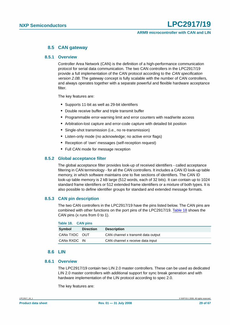
8.5.3 CAN pin description
The two CAN controllers in the LPC2917/19 have the pins listed below. The CAN pins arecombined with other functions on the port pins of the LPC2917/19. Table 18 shows theCAN pins (x runs from 0 to 1).
8.6 LIN
8.6.1 Overview
The LPC2917/19 contain two LIN 2.0 master controllers. These can be used as dedicatedLIN 2.0 master controllers with additional support for sync break generation and withhardware implementation of the LIN protocol according to spec 2.0.
The key features are:
Table 18. CAN pins
Symbol Direction Description
CANx TXDC OUT CAN channel x transmit data output
CANx RXDC IN CAN channel x receive data input
LPC2917_19_1 © NXP B.V. 2008. All rights reserved.
Product data sheet Rev. 01 — 31 July 2008 29 of 67

NXP Semiconductors LPC2917/19ARM9 microcontroller with CAN and LIN
• Complete LIN 2.0 message handling and transfer
• One interrupt per LIN message
• Slave response time-out detection
• Programmable sync-break length
• Automatic sync-field and sync-break generation
• Programmable inter-byte space
• Hardware or software parity generation
• Automatic checksum generation
• Fault confinement
• Fractional baud rate generator
8.6.2 LIN pin description
The two LIN 2.0 master controllers in the LPC2917/19 have the pins listed below. The LINpins are combined with other functions on the port pins of the LPC2917/19. Table 19shows the LIN pins. For more information see Ref. 1 subsection 3.43, LIN mastercontroller.
8.7 Modulation and sampling control subsystem
8.7.1 Overview
The Modulation and Sampling Control Subsystem (MSCSS) in the LPC2917/19 includesfour Pulse-Width Modulators (PWMs), two 10-bit successive approximationAnalog-to-Digital Converters (ADCs) and two timers.
The key features of the MSCSS are:
• Two 10-bit, 400 ksample/s, 8-channel ADCs with 3.3 V inputs and various trigger-start options
• Four 6-channel PWMs (Pulse-Width Modulators) with capture and trap functionality
• Two dedicated timers to schedule and synchronize the PWMs and ADCs
8.7.2 Description
The MSCSS contains Pulse-Width Modulators (PWMs), Analog-to-Digital Converters(ADCs) and timers.
Figure 7 provides an overview of the MSCSS. An AHB-to-APB bus bridge takes care ofcommunication with the AHB system bus. Two internal timers are dedicated to thissubsystem. MSCSS timer 0 can be used to generate start pulses for the ADCs and thefirst PWM. The second timer (MSCSS timer 1) is used to generate ‘carrier’ signals for thePWMs. These carrier patterns can be used, for example, in applications requiring current
Table 19. LIN controller pins
Symbol Direction Description
LIN0/1 TXDL OUT LIN channel 0/1 transmit data output
LIN0/1 RXDL IN LIN channel 0/1 receive data input
LPC2917_19_1 © NXP B.V. 2008. All rights reserved.
Product data sheet Rev. 01 — 31 July 2008 30 of 67

NXP Semiconductors LPC2917/19ARM9 microcontroller with CAN and LIN
control. Several other trigger possibilities are provided for the ADCs (external, cascadedor following a PWM). The capture inputs of both timers can also be used to capture thestart pulse of the ADCs.
The PWMs can be used to generate waveforms in which the frequency, duty cycle andrising and falling edges can be controlled very precisely. Capture inputs are provided tomeasure event phases compared to the main counter. Depending on the applications,these inputs can be connected to digital sensor motor outputs or digital external signals.Interrupt signals are generated on several events to closely interact with the CPU.
The ADCs can be used for any application needing accurate digitized data from analogsources. To support applications like motor control, a mechanism to synchronize severalPWMs and ADCs is available (sync_in and sync_out).
Note that the PWMs run on the PWM clock and the ADCs on the ADC clock, seeSection 8.8.4.
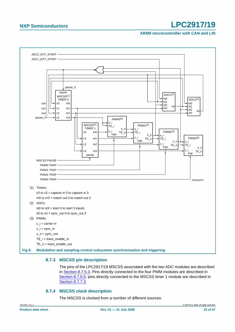
8.7.2.1 Synchronization and trigger features of the MSCSS
The MSCSS contains two internal timers to generate synchronization and carrier pulsesfor the ADCs and PWMs. Figure 8 shows how the timers are connected to the ADC andPWM modules.
Fig 7. Modulation and sampling control subsystem block diagram
002aad348
PWM0 MAT[5:0]
PWM1 MAT[5:0]
PWM2 MAT[5:0]
PWM3 MAT[5:0]
ADC1
3.3 VADC
2
3.3 V
PWM0
MSCSSTIMER 1
PWMCONTROL
CARRIERS
MSCSSTIMER 0
ADCCONTROL
SYNCS
AHB2APBBRIDGE
PWM1
PWM2
PWM3
AHBsystem bus
APB sub system bus(to all sub blocks)
ADC2 IN[7:0]ADC2_EXT_START
ADC1 IN[7:0]ADC1_EXT_START
ADC clock
PWM0 TRAPPWM0 CAP[2:0]
PWM1 TRAPPWM1 CAP[2:0]
PWM2 TRAPPWM2 CAP[2:0]
PWM3 TRAPPWM3 CAP[2:0]
LPC2917_19_1 © NXP B.V. 2008. All rights reserved.
Product data sheet Rev. 01 — 31 July 2008 31 of 67

NXP Semiconductors LPC2917/19ARM9 microcontroller with CAN and LIN
Each ADC module has four start inputs. An ADC conversion is started when one of thestart ADC conditions is valid:
• Start 0: ADC external start input pin; can be triggered at a positive or negative edge.Note that this signal is captured in the ADC clock domain
• Start 1: If the ‘preceding’ ADC conversion is ended, the sync_out signal starts an ADCconversion. This signal is captured in the MSCSS subsystem clock domain, seeSection 8.7.5.2. As can be seen in Figure 8, the sync_out of ADC1 is connected to thestart 1 input of ADC2 and the sync_out of ADC2 is connected to the start 1 input ofADC1.
• Start 2: The PWM sync_out can start an ADC conversion. The sync_out signal issynchronized to the ADC clock in the ADC module. This signal is captured in theMSCSS subsystem clock domain.
• Start 3: The match outputs from MSCSS timer 0 are connected to the start 3 inputs ofthe ADCs. This signal is captured in the ADC clock domain.
The PWM_sync and trans_enable_in of PWM 0 are connected to the 4th match output ofMSCSS timer 0 to start the PWM after a pre-programmed delay. This sync signal iscascaded through all PWMs, allowing a programmable delay offset between subsequentPWMs. The sync delay of each PWM can be programmed synchronously or with adifferent phase for spreading the power load.
The match outputs of MSCSS timer 1 (PWM control) are connected to the correspondingcarrier inputs of the PWM modules. The carrier signal is modulated with the PWM-generated waveforms.
The pause input of MSCSS timer 1 (PWM Control) is connected to an external input pin.Generation of the carrier signal is stopped by asserting the pause of this timer.
The pause input of MSCSS timer 0 (ADC Control) is connected to a ‘NOR’ of thePWM_sync outputs (start 2 input on the ADCs). If the pause feature of this timer isenabled the timer only counts when one of the PWM_sync outputs is active HIGH. Thisfeature can be used to start the ADC once every x PWM cycles, where x corresponds tothe value in the match register of the timer. In this case the start 3 input of the ADC shouldbe enabled (start on match output of MSCSS timer 0).
The signals connected to the capture inputs of the timers (both MSCSS timer 0 andMSCSS timer 1) are intended for debugging.
LPC2917_19_1 © NXP B.V. 2008. All rights reserved.
Product data sheet Rev. 01 — 31 July 2008 32 of 67
NXP Semiconductors LPC2917/19ARM9 microcontroller with CAN and LIN
8.7.3 MSCSS pin description
The pins of the LPC2917/19 MSCSS associated with the two ADC modules are describedin Section 8.7.5.3. Pins directly connected to the four PWM modules are described inSection 8.7.6.5: pins directly connected to the MSCSS timer 1 module are described inSection 8.7.7.3.
8.7.4 MSCSS clock description
The MSCSS is clocked from a number of different sources:
(1) Timers:
c0 to c3 = capture in 0 to capture in 3
m0 to m3 = match out 0 to match out 3
(2) ADCs:
st0 to st3 = start 0 to start 3 inputs
s0 to s3 = sync_out 0 to sync_out 3
(3) PWMs:
c_i = carrier in
s_i = sync_in
s_o = sync_out
TE_i = trans_enable_in
TE_o = trans_enable_out
Fig 8. Modulation and sampling-control subsystem synchronization and triggering
002aad347
MSCSS PAUSE
PWM0 TRAP
PWM1 TRAP
PWM2 TRAP
PWM3 TRAP
ADC2_EXT_START
pause_0
pause_0
so2
so1
so0
MSCSS(1)
TIMER 0
MSCSS(1)
TIMER 1
ADC1_EXT_START
c0
c1
c2
c3
m0
pause
m1
m2
m3
c0
c1
c2
c3
m0
pause
m1
m2
m3
st0
so
ADC1(2)
st1st2st3
st0
so
ADC2(2)
st1st2st3
s_i
s_oTE_o
PWM0(3)
TE_i
c_itrap
s_i
s_oTE_o
PWM1(3)
TE_i
c_itrap
s_i
s_oTE_o
PWM2(3)
TE_i
c_itrap
s_i
s_oTE_o
PWM3(3)
TE_i
c_itrap
LPC2917_19_1 © NXP B.V. 2008. All rights reserved.
Product data sheet Rev. 01 — 31 July 2008 33 of 67
NXP Semiconductors LPC2917/19ARM9 microcontroller with CAN and LIN
• CLK_SYS_MSCSS_A clocks the AHB side of the AHB-to-APB bus bridge
• CLK_MSCSS_APB clocks the subsystem APB bus
• CLK_MSCSS_MTMR0/1 clocks the timers
• CLK_MSCSS_PWM0..3 clocks the PWMs.
Each ADC has two clock areas; a APB part clocked by CLK_MSCSS_ADCx_APB (x = 1or 2) and a control part for the analog section clocked by CLK_ADCx = 1 or 2), seeSection 7.2.2.
All clocks are derived from the BASE_MSCSS_CLK, except for CLK_SYS_MSCSS_Awhich is derived form BASE_SYS_CLK, and the CLK_ADCx clocks which are derivedfrom BASE_CLK_ADC. If specific PWM or ADC modules are not used their correspondingclocks can be switched off.
8.7.5 Analog-to-digital converter
8.7.5.1 Overview
The MSCSS in the LPC2917/19 includes two 10-bit successive-approximationanalog-to-digital converters.
The key features of the ADC interface module are:
• ADC1 and ADC2: Eight analog inputs; time-multiplexed; measurement range up to3.3 V
• External reference-level inputs
• 400 ksample/s at 10-bit resolution up to 1500 ksample/s at 2-bit resolution
• Programmable resolution from 2-bit to 10-bit
• Single analog-to-digital conversion scan mode and continuous analog-to-digitalconversion scan mode
• Optional conversion on transition on external start input, timer capture/match signal,PWM_sync or ‘previous’ ADC
• Converted digital values are stored in a register for each channel
• Optional compare condition to generate a ‘less than’ or an ‘equal to or greater than’compare-value indication for each channel
• Power-down mode
8.7.5.2 Description
The ADC block diagram, Figure 9, shows the basic architecture of each ADC. The ADCfunctionality is divided into two major parts; one part running on the MSCSS Subsystemclock, the other on the ADC clock. This split into two clock domains affects the behaviorfrom a system-level perspective. The actual analog-to-digital conversions take place in theADC clock domain, but system control takes place in the system clock domain.
A mechanism is provided to modify configuration of the ADC and control the moment atwhich the updated configuration is transferred to the ADC domain.
The ADC clock is limited to 4.5 MHz maximum frequency and should always be lower thanor equal to the system clock frequency. To meet this constraint or to select the desiredlower sampling frequency the clock generation unit provides a programmable fractional
LPC2917_19_1 © NXP B.V. 2008. All rights reserved.
Product data sheet Rev. 01 — 31 July 2008 34 of 67
NXP Semiconductors LPC2917/19ARM9 microcontroller with CAN and LIN
system-clock divider dedicated to the ADC clock. Conversion rate is determined by theADC clock frequency divided by the number of resolution bits plus one. Accessing ADCregisters requires an enabled ADC clock, which is controllable via the clock generationunit, see Section 8.8.4.
Each ADC has four start inputs. Note that start 0 and start 2 are captured in the systemclock domain while start 1 and start 3 are captured in the ADC domain. The start inputsare connected at MSCSS level, see Section 8.7.2.1 for details.
8.7.5.3 ADC pin description
The two ADC modules in the MSCSS have the pins described below. The ADCx input pinsare combined with other functions on the port pins of the LPC2917/19. The VREFN andVREFP pins are common for both ADCs. Table 20 shows the ADC pins.
8.7.5.4 ADC clock description
The ADC modules are clocked from two different sources; CLK_MSCSS_ADCx_APB andCLK_ADCx (x = 1 or 2), see Section 7.2.2. Note that each ADC has its own CLK_ADCxand CLK_MSCSS_ADCx_APB branch clocks for power management. If an ADC isunused both its CLK_MSCSS_ADCx_APB and CLK_ADCx can be switched off.
Fig 9. ADC block diagram
002aad838start 2start 0
CLK_ADCx_APB(MSCSS sub-system clock)
CLK_ADCx(ADC clock
up to 4.5 MHz)
APB system bus
ADC IRQ
analog inputs
start 1 start 3sync_out
ADC DOMAINAPB SUB-SYSTEMDOMAIN
ADCCONTROL
ANDREGISTERS
ADCCONTROL
ANDREGISTERS
3.3 VADC
ANALOGMUX
conversion data
update
configuration data
IRQ
ADC1 IN[0:7]
ADC2 IN[0:7]
Table 20. Analog to digital converter pins
Symbol Direction Description
ADCn IN[7:0] IN analog input for ADCn, channel 7 to channel 0 (n is 1 or 2)
ADCn_EXT_START IN ADC external start-trigger input (n is 1 or 2)
VREFN IN ADC LOW reference level
VREFP IN ADC HIGH reference level
LPC2917_19_1 © NXP B.V. 2008. All rights reserved.
Product data sheet Rev. 01 — 31 July 2008 35 of 67

NXP Semiconductors LPC2917/19ARM9 microcontroller with CAN and LIN
The frequency of all the CLK_MSCSS_ADCx_APB clocks is identical toCLK_MSCSS_APB since they are derived from the same base clockBASE_MSCSS_CLK. Likewise the frequency of all the CLK_ADCx clocks is identicalsince they are derived from the same base clock BASE_ADC_CLK.
The register interface towards the system bus is clocked by CLK_MSCSS_ADCx_APB.Control logic for the analog section of the ADC is clocked by CLK_ADCx, see alsoFigure 9.
8.7.6 PWM
8.7.6.1 Overview
The MSCSS in the LPC2917/19 includes four PWM modules with the following features.
• Six pulse-width modulated output signals
• Double edge features (rising and falling edges programmed individually)
• Optional interrupt generation on match (each edge)
• Different operation modes: continuous or run-once
• 16-bit PWM counter and 16-bit prescale counter allow a large range of PWM periods
• A protective mode (TRAP) holding the output in a software-controllable state and withoptional interrupt generation on a trap event
• Three capture registers and capture trigger pins with optional interrupt generation ona capture event
• Interrupt generation on match event, capture event, PWM counter overflow or trapevent
• A burst mode mixing the external carrier signal with internally generated PWM
• Programmable sync-delay output to trigger other PWM modules (master/slavebehavior)
8.7.6.2 Description
The ability to provide flexible waveforms allows PWM blocks to be used in multipleapplications; e.g. automotive dimmer/lamp control and fan control. Pulse-width modulationis the preferred method for regulating power since no additional heat is generated and it isenergy-efficient when compared with linear-regulating voltage control networks.
The PWM delivers the waveforms/pulses of the desired duty cycles and cycle periods. Avery basic application of these pulses can be in controlling the amount of powertransferred to a load. Since the duty cycle of the pulses can be controlled, the desiredamount of power can be transferred for a controlled duration. Two examples of suchapplications are:
• Automotive dimmer controller: The flexibility of providing waves of a desired duty cycleand cycle period allows the PWM to control the amount of power to be transferred tothe load. The PWM functions as a dimmer controller in this application
• Motor controller: The PWM provides multi-phase outputs, and these outputs can becontrolled to have a certain pattern sequence. In this way the force/torque of themotor can be adjusted as desired. This makes the PWM function as a motor drive.
LPC2917_19_1 © NXP B.V. 2008. All rights reserved.
Product data sheet Rev. 01 — 31 July 2008 36 of 67
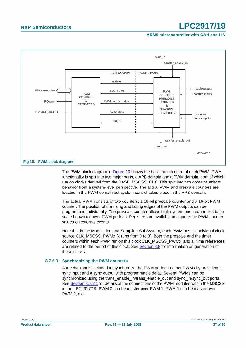
NXP Semiconductors LPC2917/19ARM9 microcontroller with CAN and LIN
The PWM block diagram in Figure 10 shows the basic architecture of each PWM. PWMfunctionality is split into two major parts, a APB domain and a PWM domain, both of whichrun on clocks derived from the BASE_MSCSS_CLK. This split into two domains affectsbehavior from a system-level perspective. The actual PWM and prescale counters arelocated in the PWM domain but system control takes place in the APB domain.
The actual PWM consists of two counters; a 16-bit prescale counter and a 16-bit PWMcounter. The position of the rising and falling edges of the PWM outputs can beprogrammed individually. The prescale counter allows high system bus frequencies to bescaled down to lower PWM periods. Registers are available to capture the PWM countervalues on external events.
Note that in the Modulation and Sampling SubSystem, each PWM has its individual clocksource CLK_MSCSS_PWMx (x runs from 0 to 3). Both the prescale and the timercounters within each PWM run on this clock CLK_MSCSS_PWMx, and all time referencesare related to the period of this clock. See Section 8.8 for information on generation ofthese clocks.
8.7.6.3 Synchronizing the PWM counters
A mechanism is included to synchronize the PWM period to other PWMs by providing async input and a sync output with programmable delay. Several PWMs can besynchronized using the trans_enable_in/trans_enable_out and sync_in/sync_out ports.See Section 8.7.2.1 for details of the connections of the PWM modules within the MSCSSin the LPC2917/19. PWM 0 can be master over PWM 1; PWM 1 can be master overPWM 2, etc.
Fig 10. PWM block diagram
002aad837
APB system bus
IRQ pwm
IRQ capt_match
PWMCONTROL
®ISTERS
update
capture data
PWM counter value
config data
IRQ's
PWM,COUNTER,PRESCALECOUNTER
&SHADOW
REGISTERS
match outputs
capture inputs
trap inputcarrier inputs
sync_in
sync_out
transfer_enable_in
transfer_enable_out
APB DOMAIN PWM DOMAIN
LPC2917_19_1 © NXP B.V. 2008. All rights reserved.
Product data sheet Rev. 01 — 31 July 2008 37 of 67
NXP Semiconductors LPC2917/19ARM9 microcontroller with CAN and LIN
8.7.6.4 Master and slave mode
A PWM module can provide synchronization signals to other modules (also called Mastermode). The signal sync_out is a pulse of one clock cycle generated when the internalPWM counter (re)starts. The signal trans_enable_out is a pulse synchronous to sync_out,generated if a transfer from system registers to PWM shadow registers occurred when thePWM counter restarted. A delay may be inserted between the counter start andgeneration of trans_enable_out and sync_out.
A PWM module can use input signals trans_enable_in and sync_in to synchronize itsinternal PWM counter and the transfer of shadow registers (Slave mode).
8.7.6.5 PWM pin description
Each of the four PWM modules in the MSCSS has the following pins. These are combinedwith other functions on the port pins of the LPC2917/19. Table 21 shows the PWM0 toPWM3 pins.
8.7.6.6 PWM clock description
The PWM modules are clocked by CLK_MSCSS_PWMx (x = 0-3), see Section 7.2.2.Note that each PWM has its own CLK_MSCSS_PWMx branch clock for powermanagement. The frequency of all these clocks is identical to CLK_MSCSS_APB sincethey are derived from the same base clock BASE_MSCSS_CLK.
Also note that unlike the timer modules in the Peripheral SubSystem, the actual timercounter registers of the PWM modules run at the same clock as the APB system interfaceCLK_MSCSS_APB. This clock is independent of the AHB system clock.
If a PWM module is not used its CLK_MSCSS_PWMx branch clock can be switched off.
8.7.7 Timers in the MSCSS
8.7.7.1 Overview
The two timers in the MSCSS are functionally identical to the timers in the peripheralsubsystem, see Section 8.4.3. The features of the timers in the MSCSS are the same asthe timers in the peripheral subsystem, but the capture inputs and match outputs are notavailable on the device pins. These signals are instead connected to the ADC and PWMmodules as outlined in the description of the MSCSS, see Section 8.7.2.
Table 21. PWM pins
Symbol Direction Description
PWMn CAP[0] IN PWM n capture input 0
PWMn CAP[1] IN PWM n capture input 1
PWMn CAP[2] IN PWM n capture input 2
PWMn MAT[0] OUT PWM n match output 0
PWMn MAT[1] OUT PWM n match output 1
PWMn MAT[2] OUT PWM n match output 2
PWMn MAT[3] OUT PWM n match output 3
PWMn MAT[4] OUT PWM n match output 4
PWMn MAT[5] OUT PWM n match output 5
PWMn TRAP IN PWM n trap input
LPC2917_19_1 © NXP B.V. 2008. All rights reserved.
Product data sheet Rev. 01 — 31 July 2008 38 of 67
NXP Semiconductors LPC2917/19ARM9 microcontroller with CAN and LIN
8.7.7.2 Description
See section Section 8.4.3.2 for a description of the timers.
8.7.7.3 MSCSS timer-pin description
MSCSS timer 0 has no external pins.
MSCSS timer 1 has a PAUSE pin available as external pin. The PAUSE pin is combinedwith other functions on the port pins of the LPC2917/19. Table 22 shows the MSCSStimer 1 external pin.
8.7.7.4 MSCSS timer-clock description
The Timer modules in the MSCSS are clocked by CLK_MSCSS_MTMRx (x = 0-1), seeSection 7.2.2. Note that each timer has its own CLK_MSCSS_MTMRx branch clock forpower management. The frequency of all these clocks is identical to CLK_MSCSS_APBsince they are derived from the same base clock BASE_MSCSS_CLK.
Note that, unlike the timer modules in the Peripheral SubSystem, the actual timer counterregisters run at the same clock as the APB system interface CLK_MSCSS_APB. Thisclock is independent of the AHB system clock.
If a timer module is not used its CLK_MSCSS_MTMRx branch clock can be switched off.
8.8 Power, clock and reset control subsystem
8.8.1 Overview
The Power, Clock and Reset Control Subsystem (PCRSS) in the LPC2917/19 includes aClock Generation Unit (CGU), a Reset Generation Unit (RGU) and a Power ManagementUnit (PMU).
8.8.2 Description
Figure 11 provides an overview of the PCRSS. An AHB-to-DTL bridge takes care ofcommunication with the AHB system bus.
Table 22. MSCSS timer 1 pin
Symbol Direction Description
MSCSS PAUSE IN pause pin for MSCSS timer 1
LPC2917_19_1 © NXP B.V. 2008. All rights reserved.
Product data sheet Rev. 01 — 31 July 2008 39 of 67

NXP Semiconductors LPC2917/19ARM9 microcontroller with CAN and LIN
Fig 11. PCRSS block diagram
002aad836
AHB2DTLBRIDGE
RESET OUTPUTDELAY LOGIC
INPUT DEGLITCH/
SYNC
branch clocks
AHB master disable grant
AHB master disable request
wakeup_a
AHB_RST
SCU_RST
WARM_RST
COLD_RSTPCR_RSTRGU_RSTPOR_RST
RST_N (device pin)
reset from watchdog counter
EXTERNALOSCILLATOR
PMUREGISTERS
CLOCKENABLE
CONTROL
CLOCKGATES
LOW POWERRING
OSCILLATOR
CGUREGISTERS
RGUREGISTERS
POR
OUT0OUT1
0UT9
PLL
FDIV[6:0]
CGU
PMU
RGU
LPC2917_19_1 © NXP B.V. 2008. All rights reserved.
Product data sheet Rev. 01 — 31 July 2008 40 of 67
NXP Semiconductors LPC2917/19ARM9 microcontroller with CAN and LIN
8.8.3 PCR subsystem clock description
The PCRSS is clocked by a number of different clocks. CLK_SYS_PCRSS clocks theAHB side of the AHB to DTL bus bridge and CLK_PCR_SLOW clocks the CGU, RGU andPMU internal logic, see Section 7.2.2. CLK_SYS_PCRSS is derived fromBASE_SYS_CLK, which can be switched off in low-power modes. CLK_PCR_SLOW isderived from BASE_PCR_CLK and is always on in order to be able to wake up fromlow-power modes.
8.8.4 Clock Generation Unit (CGU)
8.8.4.1 Overview
The key features are:
• Generation of 10 and 2 test-base clocks, selectable from several embedded clocksources
• Crystal oscillator with power-down
• Control PLL with power-down
• Very low-power ring oscillator, always on to provide a ‘safe clock’
• Seven fractional clock dividers with L/D division
• Individual source selector for each base clock, with glitch-free switching
• Autonomous clock-activity detection on every clock source
• Protection against switching to invalid or inactive clock sources
• Embedded frequency counter
• Register write-protection mechanism to prevent unintentional alteration of clocks
Remark: Any clock-frequency adjustment has a direct impact on the timing of on-boardperipherals such as the UARTs, SPI, watchdog, timers, CAN controller, LIN mastercontroller, ADCs or flash memory interface.
8.8.4.2 Description
The clock generation unit provides 10 internal clock sources as described in Table 23.
[1] Maximum frequency that guarantees stable operation of the LPC2917/19.
[2] Fixed to low-power oscillator.
Table 23. CGU base clocks
Number
Name Frequency(MHz) [1]
Description
0 BASE_SAFE_CLK 0.4 base safe clock (always on)
1 BASE_SYS_CLK 80 base system clock
2 BASE_PCR_CLK 0.4 [2] base PCR subsystem clock
3 BASE_IVNSS_CLK 80 base IVNSS subsystem clock
4 BASE_MSCSS_CLK 80 base MSCSS subsystem clock
5 BASE_UART_CLK 80 base UART clock
6 BASE_SPI_CLK 40 base SPI clock
7 BASE_TMR_CLK 80 base timers clock
8 BASE_ADC_CLK 4.5 base ADCs clock
LPC2917_19_1 © NXP B.V. 2008. All rights reserved.
Product data sheet Rev. 01 — 31 July 2008 41 of 67

NXP Semiconductors LPC2917/19ARM9 microcontroller with CAN and LIN
For generation of these base clocks, the CGU consists of primary and secondary clockgenerators and one output generator for each base clock.
There are two primary clock generators: a low-power ring oscillator (LP_OSC) and acrystal oscillator. See Figure 12.
LP_OSC is the source for the BASE_PCR_CLK that clocks the CGU itself and forBASE_SAFE_CLK that clocks a minimum of other logic in the device (like the watchdogtimer). To prevent the device from losing its clock source LP_OSC cannot be put intopower-down. The crystal oscillator can be used as source for high-frequency clocks or asan external clock input if a crystal is not connected.
Secondary clock generators are a PLL and seven fractional dividers (FDIV0..6). The PLLhas three clock outputs: normal, 120° phase-shifted and 240° phase-shifted.
Configuration of the CGU: For every output generator - generating the base clocks - achoice can be made from the primary and secondary clock generators according toFigure 13.
Fig 12. Block diagram of the CGU
LP_OSC
PLL
FDIV0
EXTERNALOSCLLLATOR
FDIV1
FDIV6
OUT 0
OUT 1
OUT 9
002aad835
clkoutclkout120clkout240
CLOCK GENERATION UNIT (CGU)
FREQUENCYMONITOR
CLOCKDETECTION
AHB TO DTL BRIDGE
LPC2917_19_1 © NXP B.V. 2008. All rights reserved.
Product data sheet Rev. 01 — 31 July 2008 42 of 67

NXP Semiconductors LPC2917/19ARM9 microcontroller with CAN and LIN
Any output generator (except for BASE_SAFE_CLK and BASE_PCR_CLK) can beconnected to either a fractional divider (FDIV0..6) or to one of the outputs of the PLL or toLP_OSC/crystal oscillator directly. BASE_SAFE_CLK and BASE_PCR_CLK can use onlyLP_OSC as source.
The fractional dividers can be connected to one of the outputs of the PLL or directly toLP_OSC/crystal Oscillator.
The PLL can be connected to the crystal oscillator.
In this way every output generating the base clocks can be configured to get the requiredclock. Multiple output generators can be connected to the same primary or secondaryclock source, and multiple secondary clock sources can be connected to the same PLLoutput or primary clock source.
Invalid selections/programming - connecting the PLL to an FDIV or to one of the PLLoutputs itself for example - will be blocked by hardware. The control register will not bewritten, the previous value will be kept, although all other fields will be written with newdata. This prevents clocks being blocked by incorrect programming.
Default Clock Sources: Every secondary clock generator or output generator isconnected to LP_OSC at reset. In this way the device runs at a low frequency after reset.It is recommended to switch BASE_SYS_CLK to a high-frequency clock generator as(one of) the first step(s) in the boot code after verifying that the high-frequency clockgenerator is running.
Clock Activity Detection: Clocks that are inactive are automatically regarded as invalid,and values of ‘CLK_SEL’ that would select those clocks are masked and not written to thecontrol registers. This is accomplished by adding a clock detector to every clockgenerator. The RDET register keeps track of which clocks are active and inactive, and the
Fig 13. Structure of the clock generation scheme
LP_OSC
PLL
FDIV0..6
EXTERNALOSCILLATOR
002aad834
clkoutclkout120clkout240
OUTPUTCONTROL
clockoutputs
LPC2917_19_1 © NXP B.V. 2008. All rights reserved.
Product data sheet Rev. 01 — 31 July 2008 43 of 67

NXP Semiconductors LPC2917/19ARM9 microcontroller with CAN and LIN
appropriate ‘CLK_SEL’ values are masked and unmasked accordingly. Each clockdetector can also generate interrupts at clock activation and deactivation so that thesystem can be notified of a change in internal clock status.
Clock detection is done using a counter running at the BASE_PCR_CLK frequency. If nopositive clock edge occurs before the counter has 32 cycles of BASE_PCR_CLK the clockis assumed to be inactive. As BASE_PCR_CLK is slower than any of the clocks to bedetected, normally only one BASE_PCR_CLK cycle is needed to detect activity. Afterreset all clocks are assumed to be ‘non-present’, so the RDET status register will becorrect only after 32 BASE_PCR_CLK cycles.
Note that this mechanism cannot protect against a currently-selected clock going fromactive to inactive state. Therefore an inactive clock may still be sent to the system underspecial circumstances, although an interrupt can still be generated to notify the system.
Glitch-Free Switching: Provisions are included in the CGU to allow clocks to be switchedglitch-free, both at the output generator stage and also at secondary source generators.
In the case of the PLL the clock will be stopped and held low for long enough to allow thePLL to stabilize and lock before being re-enabled. For all non-PLL Generators the switchwill occur as quickly as possible, although there will always be a period when the clock isheld low due to synchronization requirements.
If the current clock is high and does not go low within 32 cycles of BASE_PCR_CLK it isassumed to be inactive and is asynchronously forced low. This prevents deadlocks on theinterface.
8.8.4.3 PLL functional description
A block diagram of the PLL is shown in Figure 14. The input clock is fed directly to theanalog section. This block compares the phase and frequency of the inputs and generatesthe main clock2. These clocks are either divided by 2*P by the programmable post dividerto create the output clock, or sent directly to the output. The main output clock is thendivided by M by the programmable feedback divider to generate the feedback clock. Theoutput signal of the analog section is also monitored by the lock detector to signal whenthe PLL has locked onto the input clock.
2. Generation of the main clock is restricted by the frequency range of the PLL clock input. See Table 31, Dynamic characteristics.
Fig 14. PLL block diagram
CCO/ 2PDIV
P23
/ MDIV
002aad833
bypassdirect
clkout120clkout240clkout
clkout
input clock
PSEL bitsP23EN bit
MSEL bits
LPC2917_19_1 © NXP B.V. 2008. All rights reserved.
Product data sheet Rev. 01 — 31 July 2008 44 of 67

NXP Semiconductors LPC2917/19ARM9 microcontroller with CAN and LIN
Triple output phases: For applications that require multiple clock phases two additionalclock outputs can be enabled by setting register P23EN to logic 1, thus giving three clockswith a 120° phase difference. In this mode all three clocks generated by the analogsection are sent to the output dividers. When the PLL has not yet achieved lock thesecond and third phase output dividers run unsynchronized, which means that the phaserelation of the output clocks is unknown. When the PLL LOCK register is set the secondand third phase of the output dividers are synchronized to the main output clock CLKOUTPLL, thus giving three clocks with a 120° phase difference.
Direct output mode: In normal operating mode (with DIRECT set to logic 0) the CCOclock is divided by 2, 4, 8 or 16 depending on the value on the PSEL[1:0] input, giving anoutput clock with a 50 % duty cycle. If a higher output frequency is needed the CCO clockcan be sent directly to the output by setting DIRECT to logic 1. Since the CCO does notdirectly generate a 50 % duty cycle clock, the output clock duty cycle in this mode candeviate from 50 %.
Power-down control: A Power-down mode has been incorporated to reduce powerconsumption when the PLL clock is not needed. This is enabled by setting the PD controlregister bit. In this mode the analog section of the PLL is turned off, the oscillator and thephase-frequency detector are stopped and the dividers enter a reset state. While inPower-down mode the LOCK output is low, indicating that the PLL is not in lock. WhenPower-down mode is terminated by clearing the PD control-register bit the PLL resumesnormal operation, and makes the LOCK signal high once it has regained lock on the inputclock.
8.8.4.4 CGU pin description
The CGU module in the LPC2917/19 has the pins listed in Table 24 below.
8.8.5 Reset Generation Unit (RGU)
8.8.5.1 Overview
The key features of the Reset Generation Unit (RGU) are:
• Reset controlled individually per subsystem
• Automatic reset stretching and release
• Monitor function to trace resets back to source
• Register write-protection mechanism to prevent unintentional resets
8.8.5.2 Description
The RGU controls all internal resets.
Each reset output is defined as a (combination of) reset input sources including theexternal reset input pins and internal power-on reset, see Table 25. The first five resetslisted in this table form a sort of cascade to provide the multiple levels of impact that areset may have. The combined input sources are logically OR-ed together so thatactivating any of the listed reset sources causes the output to go active.
Table 24. CGU pins
Symbol Direction Description
XOUT_OSC OUT oscillator crystal output
XIN_OSC IN oscillator crystal input or external clock input
LPC2917_19_1 © NXP B.V. 2008. All rights reserved.
Product data sheet Rev. 01 — 31 July 2008 45 of 67

NXP Semiconductors LPC2917/19ARM9 microcontroller with CAN and LIN
8.8.5.3 RGU pin description
The RGU module in the LPC2917/19 has the following pins. Table 26 shows the RGUpins.
8.8.6 Power Management Unit (PMU)
8.8.6.1 Overview
This module enables software to actively control the system’s power consumption bydisabling clocks not required in a particular operating mode.
Using the base clocks from the CGU as input, the PMU generates branch clocks to therest of the LPC2917/19. Output clocks branched from the same base clock are phase-and frequency-related. These branch clocks can be individually controlled by softwareprogramming.
Table 25. Reset output configuration
Reset output Reset source Parts of the device reset when activated
POR_RST power-on reset module LP_OSC; is source for RGU_RST
RGU_RST POR_RST, RST_N pin RGU internal; is source for PCR_RST
PCR_RST RGU_RST, WATCHDOG PCR internal; is source for COLD_RST
COLD_RST PCR_RST parts with COLD_RST as reset source below
WARM_RST COLD_RST parts with WARM_RST as reset source below
SCU_RST COLD_RST SCU
CFID_RST COLD_RST CFID
FMC_RST COLD_RST embedded Flash Memory Controller (FMC)
EMC_RST COLD_RST embedded SRAM Memory Controller
SMC_RST COLD_RST external Static Memory Controller (SMC)
GESS_A2V_RST WARM_RST GeSS AHB-to-APB bridge
PESS_A2V_RST WARM_RST PeSS AHB-to-APB bridge
GPIO_RST WARM_RST all GPIO modules
UART_RST WARM_RST all UART modules
TMR_RST WARM_RST all Timer modules in PeSS
SPI_RST WARM_RST all SPI modules
IVNSS_A2V_RST WARM_RST IVNSS AHB-to-APB bridge
IVNSS_CAN_RST WARM_RST all CAN modules including Acceptance filter
IVNSS_LIN_RST WARM_RST all LIN modules
MSCSS_A2V_RST WARM_RST MSCSS AHB to APB bridge
MSCSS_PWM_RST WARM_RST all PWM modules
MSCSS_ADC_RST WARM_RST all ADC modules
MSCSS_TMR_RST WARM_RST all Timer modules in MSCSS
VIC_RST WARM_RST Vectored Interrupt Controller (VIC)
AHB_RST WARM_RST CPU and AHB Bus infrastructure
Table 26. RGU pins
Symbol Direction Description
RST_N IN external reset input, active LOW; pulled up internally
LPC2917_19_1 © NXP B.V. 2008. All rights reserved.
Product data sheet Rev. 01 — 31 July 2008 46 of 67
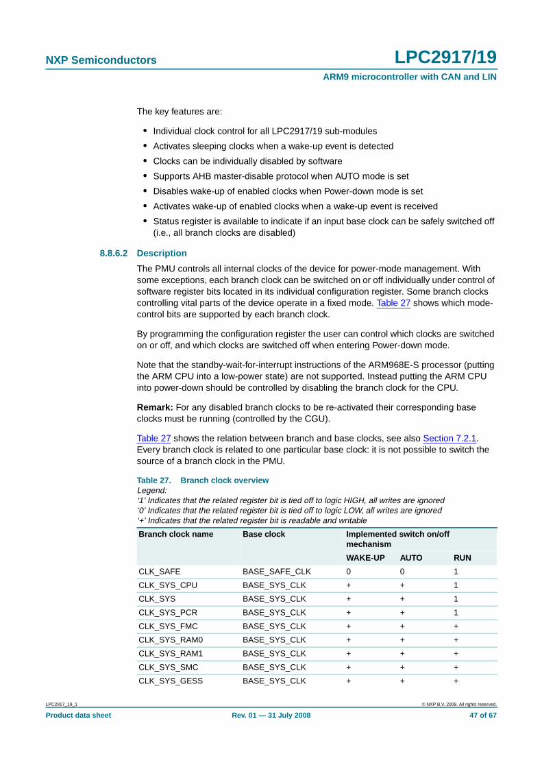
NXP Semiconductors LPC2917/19ARM9 microcontroller with CAN and LIN
The key features are:
• Individual clock control for all LPC2917/19 sub-modules
• Activates sleeping clocks when a wake-up event is detected
• Clocks can be individually disabled by software
• Supports AHB master-disable protocol when AUTO mode is set
• Disables wake-up of enabled clocks when Power-down mode is set
• Activates wake-up of enabled clocks when a wake-up event is received
• Status register is available to indicate if an input base clock can be safely switched off(i.e., all branch clocks are disabled)
8.8.6.2 Description
The PMU controls all internal clocks of the device for power-mode management. Withsome exceptions, each branch clock can be switched on or off individually under control ofsoftware register bits located in its individual configuration register. Some branch clockscontrolling vital parts of the device operate in a fixed mode. Table 27 shows which mode-control bits are supported by each branch clock.
By programming the configuration register the user can control which clocks are switchedon or off, and which clocks are switched off when entering Power-down mode.
Note that the standby-wait-for-interrupt instructions of the ARM968E-S processor (puttingthe ARM CPU into a low-power state) are not supported. Instead putting the ARM CPUinto power-down should be controlled by disabling the branch clock for the CPU.
Remark: For any disabled branch clocks to be re-activated their corresponding baseclocks must be running (controlled by the CGU).
Table 27 shows the relation between branch and base clocks, see also Section 7.2.1.Every branch clock is related to one particular base clock: it is not possible to switch thesource of a branch clock in the PMU.
Table 27. Branch clock overviewLegend:‘1’ Indicates that the related register bit is tied off to logic HIGH, all writes are ignored‘0’ Indicates that the related register bit is tied off to logic LOW, all writes are ignored‘+’ Indicates that the related register bit is readable and writable
Branch clock name Base clock Implemented switch on/offmechanism
WAKE-UP AUTO RUN
CLK_SAFE BASE_SAFE_CLK 0 0 1
CLK_SYS_CPU BASE_SYS_CLK + + 1
CLK_SYS BASE_SYS_CLK + + 1
CLK_SYS_PCR BASE_SYS_CLK + + 1
CLK_SYS_FMC BASE_SYS_CLK + + +
CLK_SYS_RAM0 BASE_SYS_CLK + + +
CLK_SYS_RAM1 BASE_SYS_CLK + + +
CLK_SYS_SMC BASE_SYS_CLK + + +
CLK_SYS_GESS BASE_SYS_CLK + + +
LPC2917_19_1 © NXP B.V. 2008. All rights reserved.
Product data sheet Rev. 01 — 31 July 2008 47 of 67

NXP Semiconductors LPC2917/19ARM9 microcontroller with CAN and LIN
CLK_SYS_VIC BASE_SYS_CLK + + +
CLK_SYS_PESS BASE_SYS_CLK + + +
CLK_SYS_GPIO0 BASE_SYS_CLK + + +
CLK_SYS_GPIO1 BASE_SYS_CLK + + +
CLK_SYS_GPIO2 BASE_SYS_CLK + + +
CLK_SYS_GPIO3 BASE_SYS_CLK + + +
CLK_SYS_IVNSS_A BASE_SYS_CLK + + +
CLK_SYS_MSCSS_A BASE_SYS_CLK + + +
CLK_SYS_CHCA BASE_SYS_CLK + + +
CLK_SYS_CHCB BASE_SYS_CLK + + +
CLK_PCR_SLOW BASE_PCR_CLK + + 1
CLK_IVNSS_APB BASE_IVNSS_CLK + + +
CLK_IVNSS_CANC0 BASE_IVNSS_CLK + + +
CLK_IVNSS_CANC1 BASE_IVNSS_CLK + + +
CLK_IVNSS_LIN0 BASE_IVNSS_CLK + + +
CLK_IVNSS_LIN1 BASE_IVNSS_CLK + + +
CLK_MSCSS_APB BASE_MSCSS_CLK + + +
CLK_MSCSS_MTMR0 BASE_MSCSS_CLK + + +
CLK_MSCSS_MTMR1 BASE_MSCSS_CLK + + +
CLK_MSCSS_PWM0 BASE_MSCSS_CLK + + +
CLK_MSCSS_PWM1 BASE_MSCSS_CLK + + +
CLK_MSCSS_PWM2 BASE_MSCSS_CLK + + +
CLK_MSCSS_PWM3 BASE_MSCSS_CLK + + +
CLK_MSCSS_ADC1_APB BASE_MSCSS_CLK + + +
CLK_MSCSS_ADC2_APB BASE_MSCSS_CLK + + +
CLK_UART0 BASE_UART_CLK + + +
CLK_UART1 BASE_UART_CLK + + +
CLK_SPI0 BASE_SPI_CLK + + +
CLK_SPI1 BASE_SPI_CLK + + +
CLK_SPI2 BASE_SPI_CLK + + +
CLK_TMR0 BASE_TMR_CLK + + +
CLK_TMR1 BASE_TMR_CLK + + +
CLK_TMR2 BASE_TMR_CLK + + +
CLK_TMR3 BASE_TMR_CLK + + +
Table 27. Branch clock overview …continuedLegend:‘1’ Indicates that the related register bit is tied off to logic HIGH, all writes are ignored‘0’ Indicates that the related register bit is tied off to logic LOW, all writes are ignored‘+’ Indicates that the related register bit is readable and writable
Branch clock name Base clock Implemented switch on/offmechanism
WAKE-UP AUTO RUN
LPC2917_19_1 © NXP B.V. 2008. All rights reserved.
Product data sheet Rev. 01 — 31 July 2008 48 of 67

NXP Semiconductors LPC2917/19ARM9 microcontroller with CAN and LIN
8.8.6.3 PMU pin description
The PMU has no external pins.
8.9 Vectored interrupt controller
8.9.1 Overview
The LPC2917/19 contains a very flexible and powerful Vectored Interrupt Controller (VIC)to interrupt the ARM processor on request.
The key features are:
• Level-active interrupt request with programmable polarity
• 56 interrupt-request inputs
• Software-interrupt request capability associated with each request input
• Observability of interrupt-request state before masking
• Software-programmable priority assignments to interrupt requests up to 15 levels
• Software-programmable routing of interrupt requests towards the ARM-processorinputs IRQ and FIQ
• Fast identification of interrupt requests through vector
• Support for nesting of interrupt service routines
8.9.2 Description
The Vectored Interrupt Controller routes incoming interrupt requests to the ARMprocessor. The interrupt target is configured for each interrupt request input of the VIC.The targets are defined as follows:
• Target 0 is ARM processor FIQ (fast interrupt service)
• Target 1 is ARM processor IRQ (standard interrupt service)
Interrupt-request masking is performed individually per interrupt target by comparing thepriority level assigned to a specific interrupt request with a target-specific prioritythreshold. The priority levels are defined as follows:
• Priority level 0 corresponds to ‘masked’ (i.e., interrupt requests with priority 0 neverlead to an interrupt)
• Priority 1 corresponds to the lowest priority
CLK_ADC1 BASE_ADC_CLK + + +
CLK_ADC2 BASE_ADC_CLK + + +
CLK_TESTSHELL_IP BASE_CLK_TESTSHELL 0 0 1
Table 27. Branch clock overview …continuedLegend:‘1’ Indicates that the related register bit is tied off to logic HIGH, all writes are ignored‘0’ Indicates that the related register bit is tied off to logic LOW, all writes are ignored‘+’ Indicates that the related register bit is readable and writable
Branch clock name Base clock Implemented switch on/offmechanism
WAKE-UP AUTO RUN
LPC2917_19_1 © NXP B.V. 2008. All rights reserved.
Product data sheet Rev. 01 — 31 July 2008 49 of 67

NXP Semiconductors LPC2917/19ARM9 microcontroller with CAN and LIN
• Priority 15 corresponds to the highest priority
Software interrupt support is provided and can be supplied for:
• Testing Real-Time Operating System (RTOS) interrupt handling without usingdevice-specific interrupt service routines
• Software emulation of an interrupt-requesting device, including interrupts
8.9.3 VIC pin description
The VIC module in the LPC2917/19 has no external pins.
8.9.4 VIC clock description
The VIC is clocked by CLK_SYS_VIC, see Section 7.2.2.
LPC2917_19_1 © NXP B.V. 2008. All rights reserved.
Product data sheet Rev. 01 — 31 July 2008 50 of 67

NXP Semiconductors LPC2917/19ARM9 microcontroller with CAN and LIN
9. Limiting values
Table 28. Limiting valuesIn accordance with the Absolute Maximum Rating System (IEC 60134).
Symbol Parameter Conditions Min Max Unit
Supply pins
Ptot total power dissipation [1] - 1 W
VDD(CORE) core supply voltage −0.5 +2.0 V
VDD(OSC_PLL) oscillator and PLL supplyvoltage
−0.5 +2.0 V
VDDA(ADC3V3) 3.3 V ADC analog supplyvoltage
−0.5 +4.6 V
VDD(IO) I/O supply voltage −0.5 +4.6 V
IDD supply current average value per supplypin
[2] - 98 mA
ISS ground current average value per groundpin
[2] - 98 mA
Input pins and I/O pins
VXIN_OSC voltage on pin XIN_OSC −0.5 +2.0 V
VI(IO) I/O input voltage [3][4][5] −0.5 VDD(IO) + 3.0 V
VI(ADC) ADC input voltage I/O port 0. [4][5] −0.5 VDDA(ADC3V3)+ 0.5
V
VVREFP voltage on pin VREFP −0.5 +3.6 V
VVREFN voltage on pin VREFN −0.5 +3.6 V
II(ADC) ADC input current average value per input pin [2] - 35 mA
Output pins and I/O pins configured as output
IOHS HIGH-level short-circuitoutput current
drive HIGH, output shortedto VSS(IO)
[9] - −33 mA
IOLS LOW-level short-circuitoutput current
drive LOW, output shortedto VDD(IO)
[9] - +38 mA
General
Tstg storage temperature −40 +150 °C
Tamb ambient temperature −40 +85 °C
Tvj virtual junction temperature [6] −40 +125 °C
Memory
nendu(fl) endurance of flash memory - 100 000 cycle
tret(fl) flash memory retention time - 20 year
LPC2917_19_1 © NXP B.V. 2008. All rights reserved.
Product data sheet Rev. 01 — 31 July 2008 51 of 67
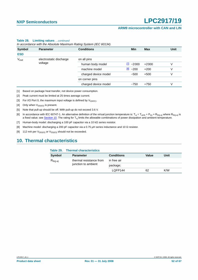
NXP Semiconductors LPC2917/19ARM9 microcontroller with CAN and LIN
[1] Based on package heat transfer, not device power consumption.
[2] Peak current must be limited at 25 times average current.
[3] For I/O Port 0, the maximum input voltage is defined by VI(ADC).
[4] Only when VDD(IO) is present.
[5] Note that pull-up should be off. With pull-up do not exceed 3.6 V.
[6] In accordance with IEC 60747-1. An alternative definition of the virtual junction temperature is: Tvj = Tamb + Ptot × Rth(j-a) where Rth(j-a) isa fixed value; see Section 10. The rating for Tvj limits the allowable combinations of power dissipation and ambient temperature.
[7] Human-body model: discharging a 100 pF capacitor via a 10 kΩ series resistor.
[8] Machine model: discharging a 200 pF capacitor via a 0.75 µH series inductance and 10 Ω resistor.
[9] 112 mA per VDD(IO) or VSS(IO) should not be exceeded.
10. Thermal characteristics
ESD
Vesd electrostatic dischargevoltage
on all pins
human body model [7] −2000 +2000 V
machine model [8] −200 +200 V
charged device model −500 +500 V
on corner pins
charged device model −750 +750 V
Table 28. Limiting values …continuedIn accordance with the Absolute Maximum Rating System (IEC 60134).
Symbol Parameter Conditions Min Max Unit
Table 29. Thermal characteristics
Symbol Parameter Conditions Value Unit
Rth(j-a) thermal resistance fromjunction to ambient
in free air
package;
LQFP144 62 K/W
LPC2917_19_1 © NXP B.V. 2008. All rights reserved.
Product data sheet Rev. 01 — 31 July 2008 52 of 67
NXP Semiconductors LPC2917/19ARM9 microcontroller with CAN and LIN
11. Static characteristics
Table 30. Static characteristicsVDD(CORE) = VDD(OSC_PLL) ; VDD(IO) = 2.7 V to 3.6 V; VDDA(ADC3V3) = 3.0 V to 3.6 V; Tvj = -40 °C to +125 °C; all voltages aremeasured with respect to ground; positive currents flow into the IC; unless otherwise specified.[1]
Symbol Parameter Conditions Min Typ Max Unit
Supplies
Core supply
VDD(CORE) core supply voltage 1.71 1.80 1.89 V
IDD(CORE) core supply current ARM9 and allperipherals active atmax clock speeds
- 1.1 2.5 mA/MHz
all clocks off [2] - 30 450 µA
I/O supply
VDD(IO) I/O supply voltage 2.7 - 3.6 V
Oscillator supply
VDD(OSC_PLL) oscillator and PLL supplyvoltage
1.71 1.80 1.89 V
IDD(OSC_PLL) oscillator and PLL supplycurrent
start-up 3 - 4.5 mA
normal mode - - 1 mA
Power-down mode - - 2 µA
Analog-to-digital converter supply
VDDA(ADC3V3) 3.3 V ADC analog supplyvoltage
3.0 3.3 3.6 V
IDDA(ADC3V3) 3.3 V ADC analog supplycurrent
normal mode - - 1.9 mA
Power-down mode - - 4 µA
Input pins and I/O pins configured as input
VI input voltage all port pins and VDD(IO)applied except port 0pins 16 to 31
see Section 9
[7][8] −0.5 - + 5.5 V
port 0 pins 16 to 31 [8] VVREFP
all port pins and VDD(IO)not applied
−0.5 - +3.6 V
all other I/O pins,RESET_N, TRST_N,TDI, JTAGSEL, TMS,TCK
−0.5 - VDD(IO) V
VIH HIGH-level input voltage all port pins, RESET_N,TRST_N, TDI,JTAGSEL, TMS, TCK
2.0 - - V
VIL LOW-level input voltage all port pins, RESET_N,TRST_N, TDI,JTAGSEL, TMS, TCK
- - 0.8 V
Vhys hysteresis voltage 0.4 - - V
ILIH HIGH-level input leakagecurrent
- - 1 µA
LPC2917_19_1 © NXP B.V. 2008. All rights reserved.
Product data sheet Rev. 01 — 31 July 2008 53 of 67
NXP Semiconductors LPC2917/19ARM9 microcontroller with CAN and LIN
ILIL LOW-level input leakagecurrent
- - 1 µA
II(pd) pull-down input current all port pins, VI = 3.3 V;VI = 5.5 V
25 50 100 µA
II(pu) pull-up input current all port pins, RESET_N,TRST_N, TDI,JTAGSEL, TMS:VI = 0 V; VI > 3.6 V is notallowed
−25 −50 −100 µA
Ci input capacitance [3] - 3 8 pF
Output pins and I/O pins configured as output
VO output voltage 0 - VDD(IO) V
VOH HIGH-level output voltage IOH = −4 mA VDD(IO) – 0.4 - - V
VOL LOW-level output voltage IOL = 4 mA - - 0.4 V
CL load capacitance - - 25 pF
Analog-to-digital converter supply
VVREFN voltage on pin VREFN 0 - VVREFP − 2 V
VVREFP voltage on pin VREFP VVREFN + 2 - VDDA(ADC3V3) V
VI(ADC) ADC input voltage on port 0 pins VVREFN - VVREFP V
Zi input impedance between VVREFN andVVREFP
4.4 - - kΩ
FSR full scale range 2 - 10 bit
INL integral non-linearity −2 - +2 LSB
DNL differential non-linearity −1 - +1 LSB
Verr(offset) offset error voltage −20 - +20 mV
Verr(FS) full-scale error voltage −20 - +20 mV
Oscillator
Rs(xtal) crystal series resistance fosc = 10 MHz to 15 MHz [5]
Cxtal = 10 pF;Cext = 18 pF
- - 160 Ω
Cxtal = 20 pF;Cext = 39 pF
- - 60 Ω
fosc = 15 MHz to 20 MHz [5]
Cxtal = 10 pF;Cext = 18 pF
- - 80 Ω
Ci input capacitance of XIN_OSC [9] - 2 pF
Table 30. Static characteristics …continuedVDD(CORE) = VDD(OSC_PLL) ; VDD(IO) = 2.7 V to 3.6 V; VDDA(ADC3V3) = 3.0 V to 3.6 V; Tvj = -40 °C to +125 °C; all voltages aremeasured with respect to ground; positive currents flow into the IC; unless otherwise specified.[1]
Symbol Parameter Conditions Min Typ Max Unit
LPC2917_19_1 © NXP B.V. 2008. All rights reserved.
Product data sheet Rev. 01 — 31 July 2008 54 of 67

NXP Semiconductors LPC2917/19ARM9 microcontroller with CAN and LIN
[1] All parameters are guaranteed over the virtual junction temperature range by design. Pre-testing is performed at Tamb = 125 °C on waferlevel. Cased products are tested at Tamb = 25 °C (final testing). Both pre-testing and final testing use correlated test conditions to coverthe specified temperature and power-supply voltage range.
[2] Leakage current is exponential to temperature; worst-case value is at 125 °C Tvj. All clocks off. Analog modules and flash powereddown.
[3] For Port 0, pin 0 to pin 15 add maximum 1.5 pF for input capacitance to ADC. For Port 0, pin 16 to pin 31 add maximum 1.0 pF for inputcapacitance to ADC.
[4] This value is the minimum drive capability. Maximum short-circuit output current is 33 mA (drive HIGH-level, shorted to ground) or−38 mA. (drive LOW-level, shorted to VDD(IO)). The device will be damaged if multiple outputs are shorted.
[5] Cxtal is crystal load capacitance and Cext are the two external load capacitors.
[6] The power-up reset has a time filter: VDD(CORE) must be above Vtrip(high) for 2 µs before reset is de-asserted; VDD(CORE) must be belowVtrip(low) for 11 µs before internal reset is asserted.
[7] Not 5 V-tolerant when pull-up is on.
[8] For I/O Port 0, the maximum input voltage is defined by VI(ADC).
[9] This parameter is not part of production testing or final testing, hence only a typical value is stated. Maximum and minimum values arebased on simulation results.
Power-up reset
Vtrip(high) high trip level voltage [6] 1.1 1.4 1.6 V
Vtrip(low) low trip level voltage [6] 1.0 1.3 1.5 V
Vtrip(dif) difference between highand low trip level voltage
[6] 50 120 180 mV
Table 30. Static characteristics …continuedVDD(CORE) = VDD(OSC_PLL) ; VDD(IO) = 2.7 V to 3.6 V; VDDA(ADC3V3) = 3.0 V to 3.6 V; Tvj = -40 °C to +125 °C; all voltages aremeasured with respect to ground; positive currents flow into the IC; unless otherwise specified.[1]
Symbol Parameter Conditions Min Typ Max Unit
LPC2917_19_1 © NXP B.V. 2008. All rights reserved.
Product data sheet Rev. 01 — 31 July 2008 55 of 67
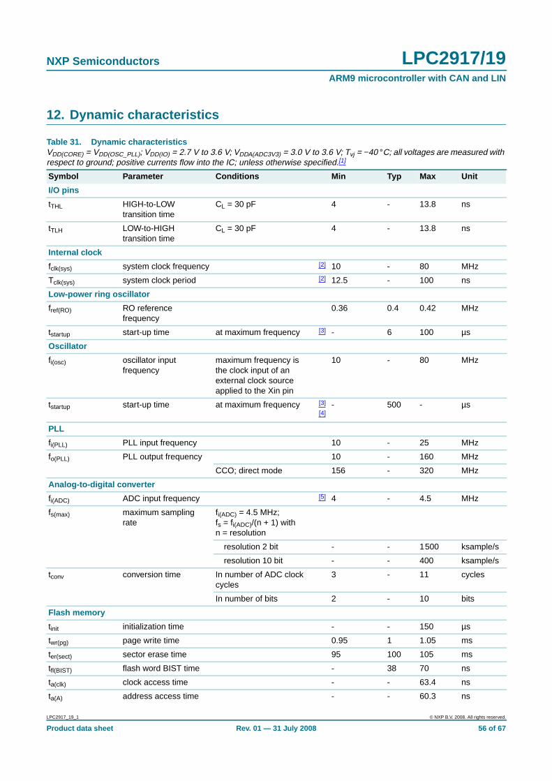
NXP Semiconductors LPC2917/19ARM9 microcontroller with CAN and LIN
12. Dynamic characteristics
Table 31. Dynamic characteristicsVDD(CORE) = VDD(OSC_PLL); VDD(IO) = 2.7 V to 3.6 V; VDDA(ADC3V3) = 3.0 V to 3.6 V; Tvj = −40 °C; all voltages are measured withrespect to ground; positive currents flow into the IC; unless otherwise specified.[1]
Symbol Parameter Conditions Min Typ Max Unit
I/O pins
tTHL HIGH-to-LOWtransition time
CL = 30 pF 4 - 13.8 ns
tTLH LOW-to-HIGHtransition time
CL = 30 pF 4 - 13.8 ns
Internal clock
fclk(sys) system clock frequency [2] 10 - 80 MHz
Tclk(sys) system clock period [2] 12.5 - 100 ns
Low-power ring oscillator
fref(RO) RO referencefrequency
0.36 0.4 0.42 MHz
tstartup start-up time at maximum frequency [3] - 6 100 µs
Oscillator
fi(osc) oscillator inputfrequency
maximum frequency isthe clock input of anexternal clock sourceapplied to the Xin pin
10 - 80 MHz
tstartup start-up time at maximum frequency [3]
[4]- 500 - µs
PLL
fi(PLL) PLL input frequency 10 - 25 MHz
fo(PLL) PLL output frequency 10 - 160 MHz
CCO; direct mode 156 - 320 MHz
Analog-to-digital converter
fi(ADC) ADC input frequency [5] 4 - 4.5 MHz
fs(max) maximum samplingrate
fi(ADC) = 4.5 MHz;fs = fi(ADC)/(n + 1) withn = resolution
resolution 2 bit - - 1500 ksample/s
resolution 10 bit - - 400 ksample/s
tconv conversion time In number of ADC clockcycles
3 - 11 cycles
In number of bits 2 - 10 bits
Flash memory
tinit initialization time - - 150 µs
twr(pg) page write time 0.95 1 1.05 ms
ter(sect) sector erase time 95 100 105 ms
tfl(BIST) flash word BIST time - 38 70 ns
ta(clk) clock access time - - 63.4 ns
ta(A) address access time - - 60.3 ns
LPC2917_19_1 © NXP B.V. 2008. All rights reserved.
Product data sheet Rev. 01 — 31 July 2008 56 of 67
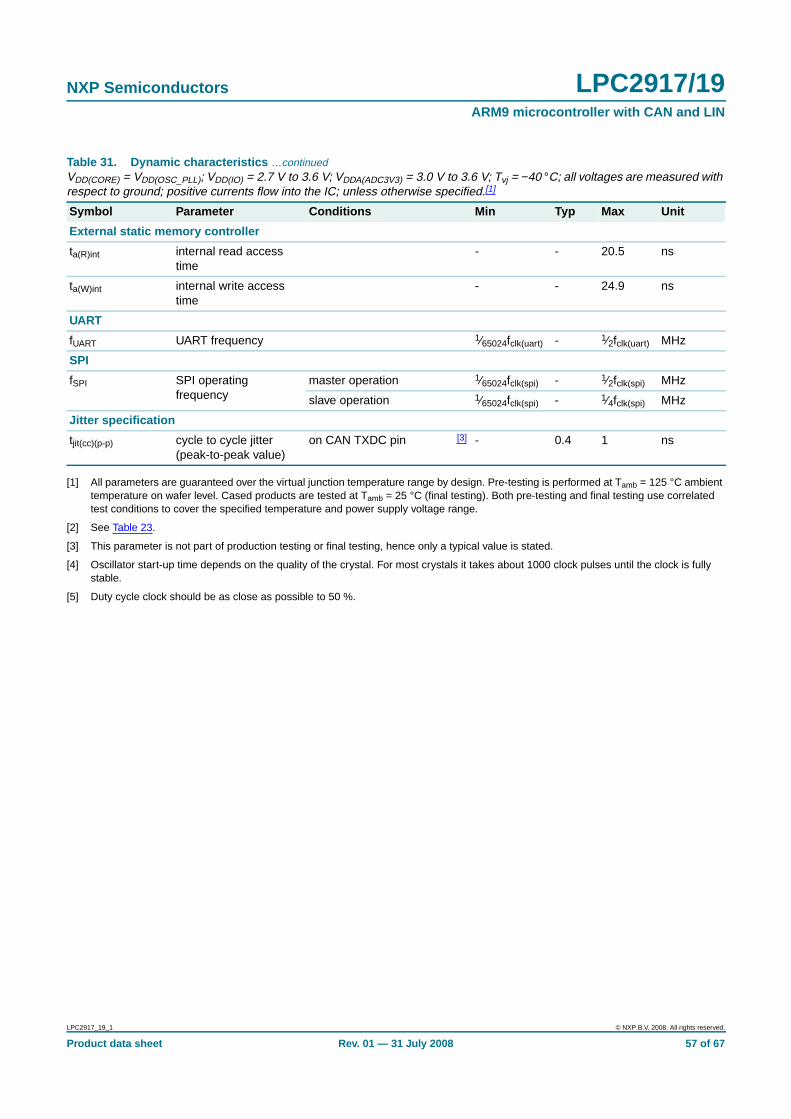
NXP Semiconductors LPC2917/19ARM9 microcontroller with CAN and LIN
[1] All parameters are guaranteed over the virtual junction temperature range by design. Pre-testing is performed at Tamb = 125 °C ambienttemperature on wafer level. Cased products are tested at Tamb = 25 °C (final testing). Both pre-testing and final testing use correlatedtest conditions to cover the specified temperature and power supply voltage range.
[2] See Table 23.
[3] This parameter is not part of production testing or final testing, hence only a typical value is stated.
[4] Oscillator start-up time depends on the quality of the crystal. For most crystals it takes about 1000 clock pulses until the clock is fullystable.
[5] Duty cycle clock should be as close as possible to 50 %.
External static memory controller
ta(R)int internal read accesstime
- - 20.5 ns
ta(W)int internal write accesstime
- - 24.9 ns
UART
fUART UART frequency 1⁄65024fclk(uart) - 1⁄2fclk(uart) MHz
SPI
fSPI SPI operatingfrequency
master operation 1⁄65024fclk(spi) - 1⁄2fclk(spi) MHz
slave operation 1⁄65024fclk(spi) - 1⁄4fclk(spi) MHz
Jitter specification
tjit(cc)(p-p) cycle to cycle jitter(peak-to-peak value)
on CAN TXDC pin [3] - 0.4 1 ns
Table 31. Dynamic characteristics …continuedVDD(CORE) = VDD(OSC_PLL); VDD(IO) = 2.7 V to 3.6 V; VDDA(ADC3V3) = 3.0 V to 3.6 V; Tvj = −40 °C; all voltages are measured withrespect to ground; positive currents flow into the IC; unless otherwise specified.[1]
Symbol Parameter Conditions Min Typ Max Unit
LPC2917_19_1 © NXP B.V. 2008. All rights reserved.
Product data sheet Rev. 01 — 31 July 2008 57 of 67

NXP Semiconductors LPC2917/19ARM9 microcontroller with CAN and LIN
13. Package outline
Fig 15. Package outline SOT486-1 (LQFP144)
UNIT A1 A2 A3 bp c E(1) e HE L L p Zywv θ
REFERENCESOUTLINEVERSION
EUROPEANPROJECTION ISSUE DATE
IEC JEDEC JEITA
mm 0.150.05
1.451.35
0.250.270.17
0.200.09
20.119.9 0.5
22.1521.85
1.41.1
70
o
o0.080.2 0.081
DIMENSIONS (mm are the original dimensions)
Note
1. Plastic or metal protrusions of 0.25 mm maximum per side are not included.
0.750.45
SOT486-1 136E23 MS-02600-03-1403-02-20
D(1) (1)(1)
20.119.9
HD
22.1521.85
EZ
1.41.1
D
0 5 10 mm
scale
bpe
θ
EA1
A
Lp
detail X
L
(A )3
B
c
bp
EH A2
DH v M B
D
ZD
A
ZE
e
v M A
Xy
w M
w M
Amax.
1.6
LQFP144: plastic low profile quad flat package; 144 leads; body 20 x 20 x 1.4 mm SOT486-1
108
109
pin 1 index
7372
371
14436
LPC2917_19_1 © NXP B.V. 2008. All rights reserved.
Product data sheet Rev. 01 — 31 July 2008 58 of 67
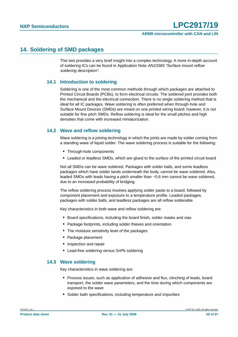
NXP Semiconductors LPC2917/19ARM9 microcontroller with CAN and LIN
14. Soldering of SMD packages
This text provides a very brief insight into a complex technology. A more in-depth accountof soldering ICs can be found in Application Note AN10365 “Surface mount reflowsoldering description”.
14.1 Introduction to solderingSoldering is one of the most common methods through which packages are attached toPrinted Circuit Boards (PCBs), to form electrical circuits. The soldered joint provides boththe mechanical and the electrical connection. There is no single soldering method that isideal for all IC packages. Wave soldering is often preferred when through-hole andSurface Mount Devices (SMDs) are mixed on one printed wiring board; however, it is notsuitable for fine pitch SMDs. Reflow soldering is ideal for the small pitches and highdensities that come with increased miniaturization.
14.2 Wave and reflow solderingWave soldering is a joining technology in which the joints are made by solder coming froma standing wave of liquid solder. The wave soldering process is suitable for the following:
• Through-hole components
• Leaded or leadless SMDs, which are glued to the surface of the printed circuit board
Not all SMDs can be wave soldered. Packages with solder balls, and some leadlesspackages which have solder lands underneath the body, cannot be wave soldered. Also,leaded SMDs with leads having a pitch smaller than ~0.6 mm cannot be wave soldered,due to an increased probability of bridging.
The reflow soldering process involves applying solder paste to a board, followed bycomponent placement and exposure to a temperature profile. Leaded packages,packages with solder balls, and leadless packages are all reflow solderable.
Key characteristics in both wave and reflow soldering are:
• Board specifications, including the board finish, solder masks and vias
• Package footprints, including solder thieves and orientation
• The moisture sensitivity level of the packages
• Package placement
• Inspection and repair
• Lead-free soldering versus SnPb soldering
14.3 Wave solderingKey characteristics in wave soldering are:
• Process issues, such as application of adhesive and flux, clinching of leads, boardtransport, the solder wave parameters, and the time during which components areexposed to the wave
• Solder bath specifications, including temperature and impurities
LPC2917_19_1 © NXP B.V. 2008. All rights reserved.
Product data sheet Rev. 01 — 31 July 2008 59 of 67
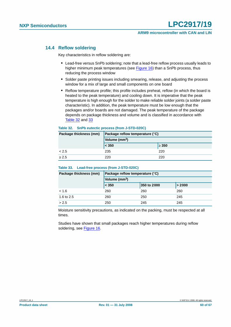
NXP Semiconductors LPC2917/19ARM9 microcontroller with CAN and LIN
14.4 Reflow solderingKey characteristics in reflow soldering are:
• Lead-free versus SnPb soldering; note that a lead-free reflow process usually leads tohigher minimum peak temperatures (see Figure 16) than a SnPb process, thusreducing the process window
• Solder paste printing issues including smearing, release, and adjusting the processwindow for a mix of large and small components on one board
• Reflow temperature profile; this profile includes preheat, reflow (in which the board isheated to the peak temperature) and cooling down. It is imperative that the peaktemperature is high enough for the solder to make reliable solder joints (a solder pastecharacteristic). In addition, the peak temperature must be low enough that thepackages and/or boards are not damaged. The peak temperature of the packagedepends on package thickness and volume and is classified in accordance withTable 32 and 33
Moisture sensitivity precautions, as indicated on the packing, must be respected at alltimes.
Studies have shown that small packages reach higher temperatures during reflowsoldering, see Figure 16.
Table 32. SnPb eutectic process (from J-STD-020C)
Package thickness (mm) Package reflow temperature ( °C)
Volume (mm 3)
< 350 ≥ 350
< 2.5 235 220
≥ 2.5 220 220
Table 33. Lead-free process (from J-STD-020C)
Package thickness (mm) Package reflow temperature ( °C)
Volume (mm 3)
< 350 350 to 2000 > 2000
< 1.6 260 260 260
1.6 to 2.5 260 250 245
> 2.5 250 245 245
LPC2917_19_1 © NXP B.V. 2008. All rights reserved.
Product data sheet Rev. 01 — 31 July 2008 60 of 67
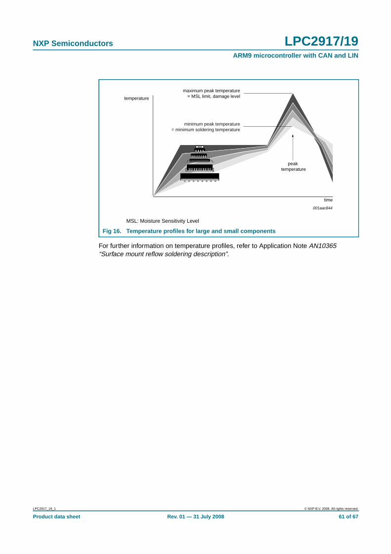
NXP Semiconductors LPC2917/19ARM9 microcontroller with CAN and LIN
For further information on temperature profiles, refer to Application Note AN10365“Surface mount reflow soldering description”.
MSL: Moisture Sensitivity Level
Fig 16. Temperature profiles for large and small components
001aac844
temperature
time
minimum peak temperature= minimum soldering temperature
maximum peak temperature= MSL limit, damage level
peak temperature
LPC2917_19_1 © NXP B.V. 2008. All rights reserved.
Product data sheet Rev. 01 — 31 July 2008 61 of 67

NXP Semiconductors LPC2917/19ARM9 microcontroller with CAN and LIN
15. Abbreviations
Table 34. Abbreviations list
Abbreviation Description
ADC Analog-to-Digital Converter
AHB Advanced High-performance Bus
AMBA Advanced Microcontroller Bus Architecture
APB ARM Peripheral Bus
BCL Buffer Control List
BDL Buffer Descriptor List
BEL Buffer Entry List
BIST Built-In Self Test
CAN Controller Area Network
CCO Current Controlled Oscillator
CISC Complex Instruction Set Computers
DAC Digital-to-Analog Converter
DTL Device Transaction Level
FIFO First In, First Out
FIQ Fast Interrupt reQuest
GPIO General Purpose Input/Output
I/O Input/Output
IAP In-Application Programming
IRQ Interrupt ReQuest
ISP In-System Programming
JTAG Joint Test Action Group
LIN Local Interconnect Network
MAC Multiply-Accumulate
PLL Phase-Locked Loop
PCRSS Power, Clock and Reset SubSystem
PWM Pulse Width Modulator
RISC Reduced Instruction Set Computer
RTOS Real-Time Operating System
RX Receive
SFSP SCU Function Select Port x,y (use without the P if there are no x,y)
SCL Slot Control List
SCU System Control Unit
SPI Serial Peripheral Interface
SSP Synchronous Serial Port
TAP Test Access Port
TCM Tightly Coupled Memory
TX Transmit
UART Universal Asynchronous Receiver Transmitter
VIC Vectored Interrupt Controller
LPC2917_19_1 © NXP B.V. 2008. All rights reserved.
Product data sheet Rev. 01 — 31 July 2008 62 of 67

NXP Semiconductors LPC2917/19ARM9 microcontroller with CAN and LIN
16. References
[1] UM — LPC2917/19 user manual
[2] ARM — ARM web site
[3] ARM-SSP — ARM primecell synchronous serial port (PL022) technical referencemanual
[4] CAN — ISO 11898-1: 2002 road vehicles - Controller Area Network (CAN) - part 1:data link layer and physical signalling
[5] LIN — LIN specification package, revision 2.0
LPC2917_19_1 © NXP B.V. 2008. All rights reserved.
Product data sheet Rev. 01 — 31 July 2008 63 of 67
NXP Semiconductors LPC2917/19ARM9 microcontroller with CAN and LIN
17. Revision history
Table 35. Revision history
Document ID Release date Data sheet status Change notice Supersedes
LPC2917_19_1 20080731 Product data sheet - -
LPC2917_19_1 © NXP B.V. 2008. All rights reserved.
Product data sheet Rev. 01 — 31 July 2008 64 of 67
NXP Semiconductors LPC2917/19ARM9 microcontroller with CAN and LIN
18. Legal information
18.1 Data sheet status
[1] Please consult the most recently issued document before initiating or completing a design.
[2] The term ‘short data sheet’ is explained in section “Definitions”.
[3] The product status of device(s) described in this document may have changed since this document was published and may differ in case of multiple devices. The latest product statusinformation is available on the Internet at URL http://www.nxp.com.
18.2 Definitions
Draft — The document is a draft version only. The content is still underinternal review and subject to formal approval, which may result inmodifications or additions. NXP Semiconductors does not give anyrepresentations or warranties as to the accuracy or completeness ofinformation included herein and shall have no liability for the consequences ofuse of such information.
Short data sheet — A short data sheet is an extract from a full data sheetwith the same product type number(s) and title. A short data sheet is intendedfor quick reference only and should not be relied upon to contain detailed andfull information. For detailed and full information see the relevant full datasheet, which is available on request via the local NXP Semiconductors salesoffice. In case of any inconsistency or conflict with the short data sheet, thefull data sheet shall prevail.
18.3 Disclaimers
General — Information in this document is believed to be accurate andreliable. However, NXP Semiconductors does not give any representations orwarranties, expressed or implied, as to the accuracy or completeness of suchinformation and shall have no liability for the consequences of use of suchinformation.
Right to make changes — NXP Semiconductors reserves the right to makechanges to information published in this document, including withoutlimitation specifications and product descriptions, at any time and withoutnotice. This document supersedes and replaces all information supplied priorto the publication hereof.
Suitability for use — NXP Semiconductors products are not designed,authorized or warranted to be suitable for use in medical, military, aircraft,space or life support equipment, nor in applications where failure ormalfunction of an NXP Semiconductors product can reasonably be expected
to result in personal injury, death or severe property or environmentaldamage. NXP Semiconductors accepts no liability for inclusion and/or use ofNXP Semiconductors products in such equipment or applications andtherefore such inclusion and/or use is at the customer’s own risk.
Applications — Applications that are described herein for any of theseproducts are for illustrative purposes only. NXP Semiconductors makes norepresentation or warranty that such applications will be suitable for thespecified use without further testing or modification.
Limiting values — Stress above one or more limiting values (as defined inthe Absolute Maximum Ratings System of IEC 60134) may cause permanentdamage to the device. Limiting values are stress ratings only and operation ofthe device at these or any other conditions above those given in theCharacteristics sections of this document is not implied. Exposure to limitingvalues for extended periods may affect device reliability.
Terms and conditions of sale — NXP Semiconductors products are soldsubject to the general terms and conditions of commercial sale, as publishedat http://www.nxp.com/profile/terms, including those pertaining to warranty,intellectual property rights infringement and limitation of liability, unlessexplicitly otherwise agreed to in writing by NXP Semiconductors. In case ofany inconsistency or conflict between information in this document and suchterms and conditions, the latter will prevail.
No offer to sell or license — Nothing in this document may be interpretedor construed as an offer to sell products that is open for acceptance or thegrant, conveyance or implication of any license under any copyrights, patentsor other industrial or intellectual property rights.
18.4 TrademarksNotice: All referenced brands, product names, service names and trademarksare the property of their respective owners.
I2C-bus — logo is a trademark of NXP B.V.
19. Contact information
For more information, please visit: http://www .nxp.com
For sales office addresses, please send an email to: salesad [email protected]
Document status [1] [2] Product status [3] Definition
Objective [short] data sheet Development This document contains data from the objective specification for product development.
Preliminary [short] data sheet Qualification This document contains data from the preliminary specification.
Product [short] data sheet Production This document contains the product specification.
LPC2917_19_1 © NXP B.V. 2008. All rights reserved.
Product data sheet Rev. 01 — 31 July 2008 65 of 67

NXP Semiconductors LPC2917/19ARM9 microcontroller with CAN and LIN
20. Contents
1 Introduction . . . . . . . . . . . . . . . . . . . . . . . . . . . . 11.1 About this document . . . . . . . . . . . . . . . . . . . . . 11.2 Intended audience . . . . . . . . . . . . . . . . . . . . . . 12 General description . . . . . . . . . . . . . . . . . . . . . . 12.1 Architectural overview. . . . . . . . . . . . . . . . . . . . 12.2 ARM968E-S processor . . . . . . . . . . . . . . . . . . . 22.3 On-chip flash memory system . . . . . . . . . . . . . 22.4 On-chip static RAM. . . . . . . . . . . . . . . . . . . . . . 33 Features . . . . . . . . . . . . . . . . . . . . . . . . . . . . . . . 33.1 General . . . . . . . . . . . . . . . . . . . . . . . . . . . . . . . 34 Ordering information . . . . . . . . . . . . . . . . . . . . . 44.1 Ordering options . . . . . . . . . . . . . . . . . . . . . . . . 45 Block diagram . . . . . . . . . . . . . . . . . . . . . . . . . . 56 Pinning information . . . . . . . . . . . . . . . . . . . . . . 66.1 Pinning . . . . . . . . . . . . . . . . . . . . . . . . . . . . . . . 66.2 Pin description . . . . . . . . . . . . . . . . . . . . . . . . . 66.2.1 General description. . . . . . . . . . . . . . . . . . . . . . 66.2.2 LQFP144 pin assignment . . . . . . . . . . . . . . . . . 67 Functional description . . . . . . . . . . . . . . . . . . 107.1 Reset, debug, test and power description . . . 107.1.1 Reset and power-up behavior. . . . . . . . . . . . . 107.1.2 Reset strategy. . . . . . . . . . . . . . . . . . . . . . . . . 107.1.3 IEEE 1149.1 interface pins (JTAG
boundary-scan test) . . . . . . . . . . . . . . . . . . . . 117.1.4 Power supply pins description . . . . . . . . . . . . 117.2 Clocking strategy . . . . . . . . . . . . . . . . . . . . . . 117.2.1 Clock architecture . . . . . . . . . . . . . . . . . . . . . . 117.2.2 Base clock and branch clock relationship . . . . 128 Block description. . . . . . . . . . . . . . . . . . . . . . . 148.1 Flash memory controller . . . . . . . . . . . . . . . . . 148.1.1 Overview. . . . . . . . . . . . . . . . . . . . . . . . . . . . . 148.1.2 Description . . . . . . . . . . . . . . . . . . . . . . . . . . . 158.1.3 Flash memory controller pin description. . . . . 168.1.4 Flash memory controller clock description . . . 168.1.5 Flash layout. . . . . . . . . . . . . . . . . . . . . . . . . . . 168.1.6 Flash bridge wait-states . . . . . . . . . . . . . . . . . 178.2 External static memory controller . . . . . . . . . . 178.2.1 Overview. . . . . . . . . . . . . . . . . . . . . . . . . . . . . 178.2.2 Description . . . . . . . . . . . . . . . . . . . . . . . . . . . 188.2.3 External static-memory controller pin
description . . . . . . . . . . . . . . . . . . . . . . . . . . . 198.2.4 External static-memory controller clock
description . . . . . . . . . . . . . . . . . . . . . . . . . . . 198.2.5 External memory timing diagrams . . . . . . . . . 198.3 General subsystem. . . . . . . . . . . . . . . . . . . . . 218.3.1 General subsystem clock description . . . . . . . 21
8.3.2 Chip and feature identification . . . . . . . . . . . . 218.3.2.1 Overview . . . . . . . . . . . . . . . . . . . . . . . . . . . . 218.3.2.2 Description . . . . . . . . . . . . . . . . . . . . . . . . . . . 218.3.2.3 CFID pin description. . . . . . . . . . . . . . . . . . . . 218.3.3 System control unit. . . . . . . . . . . . . . . . . . . . . 218.3.3.1 Overview . . . . . . . . . . . . . . . . . . . . . . . . . . . . 218.3.3.2 Description . . . . . . . . . . . . . . . . . . . . . . . . . . . 218.3.3.3 SCU pin description . . . . . . . . . . . . . . . . . . . 218.3.4 Event router . . . . . . . . . . . . . . . . . . . . . . . . . . 218.3.4.1 Overview . . . . . . . . . . . . . . . . . . . . . . . . . . . . 218.3.4.2 Description . . . . . . . . . . . . . . . . . . . . . . . . . . . 228.3.4.3 Event-router pin description and mapping
to register bit positions . . . . . . . . . . . . . . . . . . 228.4 Peripheral subsystem. . . . . . . . . . . . . . . . . . . 228.4.1 Peripheral subsystem clock description . . . . . 228.4.2 Watchdog timer . . . . . . . . . . . . . . . . . . . . . . . 238.4.2.1 Overview . . . . . . . . . . . . . . . . . . . . . . . . . . . . 238.4.2.2 Description . . . . . . . . . . . . . . . . . . . . . . . . . . . 238.4.2.3 Pin description . . . . . . . . . . . . . . . . . . . . . . . . 238.4.2.4 Watchdog timer clock description. . . . . . . . . . 238.4.3 Timer . . . . . . . . . . . . . . . . . . . . . . . . . . . . . . . 248.4.3.1 Overview . . . . . . . . . . . . . . . . . . . . . . . . . . . . 248.4.3.2 Description . . . . . . . . . . . . . . . . . . . . . . . . . . . 248.4.3.3 Pin description . . . . . . . . . . . . . . . . . . . . . . . . 248.4.3.4 Timer clock description . . . . . . . . . . . . . . . . . 258.4.4 UARTs . . . . . . . . . . . . . . . . . . . . . . . . . . . . . . 258.4.4.1 Overview . . . . . . . . . . . . . . . . . . . . . . . . . . . . 258.4.4.2 Description . . . . . . . . . . . . . . . . . . . . . . . . . . . 258.4.4.3 UART pin description . . . . . . . . . . . . . . . . . . . 258.4.4.4 UART clock description . . . . . . . . . . . . . . . . . 268.4.5 Serial peripheral interface . . . . . . . . . . . . . . . 268.4.5.1 Overview . . . . . . . . . . . . . . . . . . . . . . . . . . . . 268.4.5.2 Functional description . . . . . . . . . . . . . . . . . . 268.4.5.3 Modes of operation . . . . . . . . . . . . . . . . . . . . 278.4.5.4 SPI pin description . . . . . . . . . . . . . . . . . . . . . 278.4.5.5 SPI clock description . . . . . . . . . . . . . . . . . . . 278.4.6 General-purpose I/O . . . . . . . . . . . . . . . . . . . 288.4.6.1 Overview . . . . . . . . . . . . . . . . . . . . . . . . . . . . 288.4.6.2 Description . . . . . . . . . . . . . . . . . . . . . . . . . . . 288.4.6.3 GPIO pin description . . . . . . . . . . . . . . . . . . . 288.4.6.4 GPIO clock description. . . . . . . . . . . . . . . . . . 288.5 CAN gateway . . . . . . . . . . . . . . . . . . . . . . . . . 298.5.1 Overview . . . . . . . . . . . . . . . . . . . . . . . . . . . . 298.5.2 Global acceptance filter . . . . . . . . . . . . . . . . . 298.5.3 CAN pin description . . . . . . . . . . . . . . . . . . . . 298.6 LIN . . . . . . . . . . . . . . . . . . . . . . . . . . . . . . . . . 298.6.1 Overview . . . . . . . . . . . . . . . . . . . . . . . . . . . . 298.6.2 LIN pin description . . . . . . . . . . . . . . . . . . . . . 30
LPC2917_19_1 © NXP B.V. 2008. All rights reserved.
Product data sheet Rev. 01 — 31 July 2008 66 of 67
continued >>

NXP Semiconductors LPC2917/19ARM9 microcontroller with CAN and LIN
8.7 Modulation and sampling control subsystem . 308.7.1 Overview. . . . . . . . . . . . . . . . . . . . . . . . . . . . . 308.7.2 Description . . . . . . . . . . . . . . . . . . . . . . . . . . . 308.7.2.1 Synchronization and trigger features of
the MSCSS. . . . . . . . . . . . . . . . . . . . . . . . . . . 318.7.3 MSCSS pin description. . . . . . . . . . . . . . . . . . 338.7.4 MSCSS clock description . . . . . . . . . . . . . . . . 338.7.5 Analog-to-digital converter . . . . . . . . . . . . . . . 348.7.5.1 Overview. . . . . . . . . . . . . . . . . . . . . . . . . . . . . 348.7.5.2 Description . . . . . . . . . . . . . . . . . . . . . . . . . . . 348.7.5.3 ADC pin description . . . . . . . . . . . . . . . . . . . . 358.7.5.4 ADC clock description. . . . . . . . . . . . . . . . . . . 358.7.6 PWM. . . . . . . . . . . . . . . . . . . . . . . . . . . . . . . . 368.7.6.1 Overview. . . . . . . . . . . . . . . . . . . . . . . . . . . . . 368.7.6.2 Description . . . . . . . . . . . . . . . . . . . . . . . . . . . 368.7.6.3 Synchronizing the PWM counters. . . . . . . . . . 378.7.6.4 Master and slave mode. . . . . . . . . . . . . . . . . . 388.7.6.5 PWM pin description. . . . . . . . . . . . . . . . . . . . 388.7.6.6 PWM clock description . . . . . . . . . . . . . . . . . . 388.7.7 Timers in the MSCSS . . . . . . . . . . . . . . . . . . . 388.7.7.1 Overview. . . . . . . . . . . . . . . . . . . . . . . . . . . . . 388.7.7.2 Description . . . . . . . . . . . . . . . . . . . . . . . . . . . 398.7.7.3 MSCSS timer-pin description . . . . . . . . . . . . . 398.7.7.4 MSCSS timer-clock description . . . . . . . . . . . 398.8 Power, clock and reset control subsystem . . . 398.8.1 Overview. . . . . . . . . . . . . . . . . . . . . . . . . . . . . 398.8.2 Description . . . . . . . . . . . . . . . . . . . . . . . . . . . 398.8.3 PCR subsystem clock description . . . . . . . . . 418.8.4 Clock Generation Unit (CGU) . . . . . . . . . . . . . 418.8.4.1 Overview. . . . . . . . . . . . . . . . . . . . . . . . . . . . . 418.8.4.2 Description . . . . . . . . . . . . . . . . . . . . . . . . . . . 418.8.4.3 PLL functional description . . . . . . . . . . . . . . . 448.8.4.4 CGU pin description . . . . . . . . . . . . . . . . . . . . 458.8.5 Reset Generation Unit (RGU). . . . . . . . . . . . . 458.8.5.1 Overview. . . . . . . . . . . . . . . . . . . . . . . . . . . . . 458.8.5.2 Description . . . . . . . . . . . . . . . . . . . . . . . . . . . 458.8.5.3 RGU pin description . . . . . . . . . . . . . . . . . . . . 468.8.6 Power Management Unit (PMU) . . . . . . . . . . . 468.8.6.1 Overview. . . . . . . . . . . . . . . . . . . . . . . . . . . . . 468.8.6.2 Description . . . . . . . . . . . . . . . . . . . . . . . . . . . 478.8.6.3 PMU pin description . . . . . . . . . . . . . . . . . . . . 498.9 Vectored interrupt controller . . . . . . . . . . . . . . 498.9.1 Overview. . . . . . . . . . . . . . . . . . . . . . . . . . . . . 498.9.2 Description . . . . . . . . . . . . . . . . . . . . . . . . . . . 498.9.3 VIC pin description . . . . . . . . . . . . . . . . . . . . . 508.9.4 VIC clock description . . . . . . . . . . . . . . . . . . . 509 Limiting values. . . . . . . . . . . . . . . . . . . . . . . . . 5110 Thermal characteristics. . . . . . . . . . . . . . . . . . 5211 Static characteristics. . . . . . . . . . . . . . . . . . . . 5312 Dynamic characteristics . . . . . . . . . . . . . . . . . 56
13 Package outline . . . . . . . . . . . . . . . . . . . . . . . . 5814 Soldering of SMD packages . . . . . . . . . . . . . . 5914.1 Introduction to soldering. . . . . . . . . . . . . . . . . 5914.2 Wave and reflow soldering . . . . . . . . . . . . . . . 5914.3 Wave soldering. . . . . . . . . . . . . . . . . . . . . . . . 5914.4 Reflow soldering. . . . . . . . . . . . . . . . . . . . . . . 6015 Abbreviations . . . . . . . . . . . . . . . . . . . . . . . . . 6216 References . . . . . . . . . . . . . . . . . . . . . . . . . . . . 6317 Revision history . . . . . . . . . . . . . . . . . . . . . . . 6418 Legal information . . . . . . . . . . . . . . . . . . . . . . 6518.1 Data sheet status . . . . . . . . . . . . . . . . . . . . . . 6518.2 Definitions . . . . . . . . . . . . . . . . . . . . . . . . . . . 6518.3 Disclaimers. . . . . . . . . . . . . . . . . . . . . . . . . . . 6518.4 Trademarks . . . . . . . . . . . . . . . . . . . . . . . . . . 6519 Contact information . . . . . . . . . . . . . . . . . . . . 6520 Contents. . . . . . . . . . . . . . . . . . . . . . . . . . . . . . 66
© NXP B.V. 2008. All rights reserved.For more information, please visit: http://www.nxp.comFor sales office addresses, please send an email to: [email protected]
Date of release: 31 July 2008
Document identifier: LPC2917_19_1
Please be aware that important notices concerning this document and the product(s)described herein, have been included in section ‘Legal information’.


![LPC2921/2923/2925 ARM9 microcontroller with CAN, LIN, and …31[1] gpio1, pin 17 timer2 cap3 spi0 sdi - vss(io) 32 ground for i/o p1[16]/cap2[2]/ sck0 33[1] gpio1, pin 16 timer2 cap2](https://static.fdocuments.us/doc/165x107/60572ed1859468501a18364b/lpc292129232925-arm9-microcontroller-with-can-lin-and-311-gpio1-pin-17-timer2.jpg)


![LPC2921/2923/2925 ARM9 microcontroller with CAN, LIN, and … · p1[21]/cap3[3]/ cap1[3] 27[1] gpio1, pin 21 timer3 cap3 timer1 cap3, mscss pause-p1[20]/cap3[2]/ scs0[1] 28[1] gpio1,](https://static.fdocuments.us/doc/165x107/6054f4e7c13b2d3f9f75c9fd/lpc292129232925-arm9-microcontroller-with-can-lin-and-p121cap33-cap13.jpg)