LPC-P11C24 - Olimex 2012 LPC-P11C24 user's manual Table of Contents DISCLAIMER CHAPTER 1: OVERVIEW...
26
LPC-P11C24 CORTEX-M0 Development board USER’S MANUAL Revision C, March 2013 Designed by OLIMEX Ltd, 2012 All boards produced by Olimex LTD are ROHS compliant
Transcript of LPC-P11C24 - Olimex 2012 LPC-P11C24 user's manual Table of Contents DISCLAIMER CHAPTER 1: OVERVIEW...
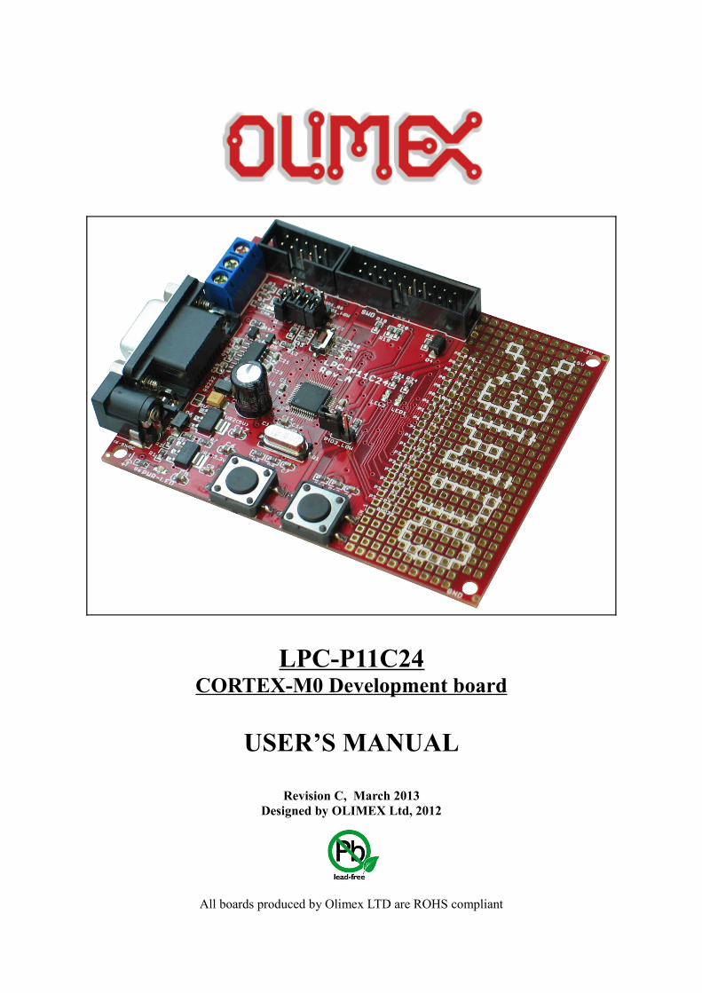
LPC-P11C24CORTEX-M0 Development board
USER’S MANUAL
Revision C, March 2013Designed by OLIMEX Ltd, 2012
All boards produced by Olimex LTD are ROHS compliant
OLIMEX© 2012 LPC-P11C24 user's manual
DISCLAIMER
© 2013 Olimex Ltd. Olimex®, logo and combinations thereof, are registered trademarks of Olimex Ltd. Other product names may be trademarks of others and the rights belong to their respective owners.
The information in this document is provided in connection with Olimex products. No license, express or implied or otherwise, to any intellectual property right is granted by this document or in connection with the sale of Olimex products.
It is possible that the pictures in this manual differ from the latest revision of the board.
The product described in this document is subject to continuous development and improvements. All particulars of the product and its use contained in this document are given by OLIMEX in good faith. However all warranties implied or expressed including but not limited to implied warranties of merchantability or fitness for purpose are excluded. This document is intended only to assist the reader in the use of the product. OLIMEX Ltd. shall not be liable for any loss or damage arising from the use of any information in this document or any error or omission in such information or any incorrect use of the product.
This evaluation board/kit is intended for use for engineering development, demonstration, or evaluation purposes only and is not considered by OLIMEX to be a finished end-product fit for general consumer use. Persons handling the product must have electronics training and observe good engineering practice standards. As such, the goods being provided are not intended to be complete in terms of required design-, marketing-, and/or manufacturing-related protective considerations, including product safety and environmental measures typically found in end products that incorporate such semiconductor components or circuit boards.
Olimex currently deals with a variety of customers for products, and therefore our arrangement with the user is not exclusive. Olimex assumes no liability for applications assistance, customer product design, software performance, or infringement of patents or services described herein.
THERE IS NO WARRANTY FOR THE DESIGN MATERIALS AND THE COMPONENTS USED TO CREATE LPC-P11C24. THEY ARE CONSIDERED SUITABLE ONLY FOR LPC-11C24.
Page 2 of 26
OLIMEX© 2012 LPC-P11C24 user's manual
Table of ContentsDISCLAIMER ............................................................................................................... CHAPTER 1: OVERVIEW ..........................................................................................
1. Introduction to the chapter ......................................................................................................... 1.1 Features .......................................................................................................................................
1.2 Target market and purpose of the board ................................................................................. 1.3 Organization ...............................................................................................................................
CHAPTER 2: SETTING UP THE LPC-P11C24 BOARD ........................................ 2. Introduction to the chapter .........................................................................................................
2.1 Electrostatic warning ................................................................................................................. 2.2 Requirements .............................................................................................................................
2.3 Powering the board .................................................................................................................... 2.4 Prebuilt software and bootloader .............................................................................................
CHAPTER 3: LPC-P11C24 BOARD DESCRIPTION .............................................. 3. Introduction to the chapter .........................................................................................................
3.1 Layout (top view) .......................................................................................................................
CHAPTER 4: THE LPC11C24 MICROCONTROLLER ......................................... 4. Introduction to the chapter ......................................................................................................... 4.1 The microcontroller ...................................................................................................................
CHAPTER 5: CONTROL CIRCUITY ....................................................................... 5. Introduction to the chapter .........................................................................................................
5.1 Reset ............................................................................................................................................ 5.2 Clocks ..........................................................................................................................................
5.3 Power supply circuit ..................................................................................................................
CHAPTER 6: CONNECTORS AND PINOUT .......................................................... 6. Introduction to the chapter ......................................................................................................... 6.1 SWD debug connector ...............................................................................................................
6.2 UEXT connector ......................................................................................................................... 6.3 Proto area pads ..........................................................................................................................
6.4 RS232 .......................................................................................................................................... 6.5 PWR Jack ...................................................................................................................................
6.8 CAN interface ............................................................................................................................. 6.12 Jumper description ..................................................................................................................
6.12.1 PIO1_LOW ............................................................................................................................ 6.12.2 PIO3_LOW ............................................................................................................................
6.12.3 PIO1_RS and RST_E ........................................................................................................... 6.12.4 SILENT/NORMAL ..............................................................................................................
6.12.5 5V_DIS ...................................................................................................................................
Page 3 of 26
OLIMEX© 2012 LPC-P11C24 user's manual
6.12.6 CAN_T ...................................................................................................................................
6.13 Additional hardware components ..........................................................................................
CHAPTER 7: BLOCK DIAGRAM AND MEMORY ............................................... 7. Introduction to the chapter ......................................................................................................... 7.2 Processor block diagram ...........................................................................................................
7.3 Physical memory map ...............................................................................................................
CHAPTER 8: SCHEMATICS ...................................................................................... 8. Introduction to the chapter ......................................................................................................... 8.1 Eagle schematic ..........................................................................................................................
8.2 Physical dimensions ...................................................................................................................
CHAPTER 9: REVISION HISTORY AND SUPPORT ............................................ 9. Introduction to the chapter ......................................................................................................... 9.1 Document revision .....................................................................................................................
9.2 Board revision ............................................................................................................................ 9.3 Useful web links and purchase codes .......................................................................................
9.3 Product support .........................................................................................................................
Page 4 of 26
OLIMEX© 2012 LPC-P11C24 user's manual
CHAPTER 1: OVERVIEW
1. Introduction to the chapter
Thank you for choosing the LPC-P11C24 development board from Olimex! This document provides a user’s guide for the Olimex LPC-P11C24 board. As an overview, this chapter gives the scope of this document and lists the board’s features. The document’s organization is then detailed.
The LPC-P11C24 development board enables code development of applications running on the microcontroller LPC11C24, manufactured by NXP Semiconductors.
1.1 Features
MCU: LPC11C24 Cortex-M0, up to 50 Mhz, 32 kB Flash, 8kB SRAM, CAN,UART RS-485, two SSP, I2C/Fast+, ADC
Power supply circuit
Power-on led
CAN interface
RS232 interface
Debug interface – SWD (Serial Wire Debug)
UEXT connector
Two user leds
Two user buttons
Reset button
Prototype area
Variable input voltage
FR-4, 1.5 mm, soldermask, component print
Dimensions: 92x72mm (3.6 x 2.8")
1.2 Target market and purpose of the board
The LPC-P11C24 is a development board with prototyping area. It is suitable for hobbyists in the fields of ARM development.
The strong points of the board are the CAN interface, the built-in bootloader, the proto area and the low price.
The software for the boards is released under General Purpose License.
Page 5 of 26
OLIMEX© 2012 LPC-P11C24 user's manual
1.3 Organization
Each section in this document covers a separate topic, organized as follows:
– Chapter 1 is an overview of the board usage and features
– Chapter 2 provides a guide for quickly setting up the board and software notes
– Chapter 3 contains the general board diagram and layout
– Chapter 4 describes the component that is the heart of the board: the LPC11C14 microcontroller
– Chapter 5 is an explanation of the control circuitry associated with the microcontroller to reset. Also shows the clocks on the board
– Chapter 6 covers the connector pinout, peripherals and jumper description
– Chapter 7 shows the memory map
– Chapter 8 provides the schematics
– Chapter 9 contains the revision history, useful links and support information
Page 6 of 26
OLIMEX© 2012 LPC-P11C24 user's manual
CHAPTER 2: SETTING UP THE LPC-P11C24 BOARD
2. Introduction to the chapter
This section helps you set up the LPC-P11C24 development board for the first time. Please consider first the electrostatic warning to avoid damaging the board, then discover the hardware and software required to operate the board.
The procedure to power up the board is given, and a description of the default board behavior is detailed.
2.1 Electrostatic warning
LPC-P11C24 is shipped in a protective anti-static package. The board must not be exposed to high electrostatic potentials. A grounding strap or similar protective device should be worn when handling the board. Avoid touching the component pins or any other metallic element.
2.2 Requirements
In order to set up the LPC-P11C24 optimally, the following items are required:
- 7V to 9V source of power with 1A maximum amperage.
- Personal Computer with RS232 port
- RS232-RS232 cable
- TRACE/SWD interface programmer for custom code
Code can be loaded via the RS232-RS232 interface and the bootloader, however it is highly recommended to have a SWD/TRACE programmer at your disposal.
Note that OpenOCD OLIMEX programmers + SWD adapter at the moment of writing are supported only in Rowleys Crossworks for ARM.
Page 7 of 26
OLIMEX© 2012 LPC-P11C24 user's manual
2.3 Powering the board
The board is powered via the PWR jack by 7 to 9 volts (preferably closer to the upper limit if you use all peripherals and GPIOs).
When powered by 9V the current measured is around 40mA. The red, green and yellow leds (PWR LED, LED1 and LED2) turn on.
2.4 Prebuilt software and bootloader
The prebuilt software is a bootloader and a simple LEDs and buttons test. When you power the board initially all LEDs will be on. If you press and hold the B1 button LED2 should start blinking. If you press and hold WAKE_UP button LED1 should start blinking. Upon releasing the buttons the LEDs should return to their initial “always on” state.
In order to connect with the bootloader you should close PIO1_RS and RST_E jumpers. You will also need RS232 cable and RS232 computer port. After that you can use NXP's FlashMagic software to check if the board is connected successfully. You can also load binary files via the RS232 using the FlashMagic.
Page 8 of 26
OLIMEX© 2012 LPC-P11C24 user's manual
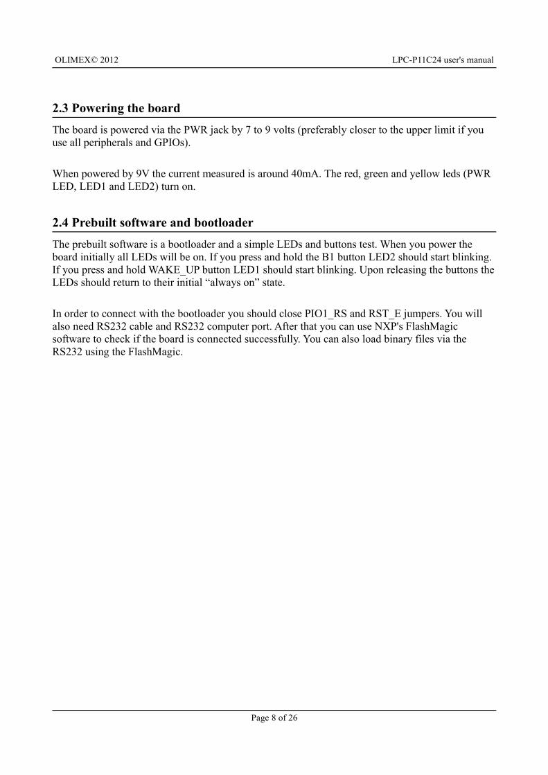
CHAPTER 3: LPC-P11C24 BOARD DESCRIPTION
3. Introduction to the chapter
Here you get acquainted with the main parts of the board. Note the names used on the board might differ from the names used below to describe them. For the actual names check the LPC-P11C24 board itself.
3.1 Layout (top view)
Page 9 of 26
OLIMEX© 2012 LPC-P11C24 user's manual
CHAPTER 4: THE LPC11C24 MICROCONTROLLER
4. Introduction to the chapter
In this chapter is located the information about the heart of LPC-P11C24 – its microcontroller. The information is a modified version of the datasheet provided by its manufacturers.
4.1 The microcontroller
System:
✔ ARM Cortex-M0 processor, running at frequencies of up to 50 MHz.
✔ ARM Cortex-M0 built-in Nested Vectored Interrupt Controller (NVIC).
✔ Serial Wire Debug.
✔ System tick timer.
Memory:
✔ 32 kB on-chip flash program memory.
✔ 8 kB SRAM data memory.
✔ In-System Programming (ISP) and In-Application Programming (IAP) via on-chip
bootloader software.Flash ISP commands can be issued via UART or C_CAN.
Digital peripherals:
✔ General Purpose I/O (GPIO) pins with configurable pull-up/pull-down resistors.
✔ 36 GPIO pins on the LPC11C24 parts.
✔ GPIO pins can be used as edge and level sensitive interrupt sources.
✔ High-current output driver (20 mA) on one pin.
✔ High-current sink drivers (20 mA) on two I2C-bus pins in Fast-mode Plus.
Four general purpose counter/timers with a total of four capture inputs 12 match outputs.
Programmable WatchDog Timer (WDT).
✔ Analog peripherals:
✔ 10-bit ADC with input multiplexing among 8 pins.
Serial interfaces:
✔ UART with fractional baud rate generation, internal FIFO, and RS-485 support.
✔ Two SPI controllers with SSP features and with FIFO and multi-protocol capabilities.
✔ I2C-bus interface supporting full I2C-bus specification and Fast-mode Plus with a data rate of 1 Mbit/s with multiple address recognition and monitor mode.
✔ C_CAN controller. On-chip C_CAN and CANopen drivers included.
✔ On-chip, high-speed CAN transceiver.
Clock generation:
Page 10 of 26

OLIMEX© 2012 LPC-P11C24 user's manual
✔ 12 MHz internal RC oscillator trimmed to 1 % accuracy that can optionally be used as a system clock.
✔ Crystal oscillator with an operating range of 1 MHz to 25 MHz.
✔ Programmable watchdog oscillator with a frequency range of 7.8 kHz to 1.8 MHz.
✔ PLL allows CPU operation up to the maximum CPU rate without the need for a high-frequency crystal. May be run from the system oscillator or the internal RC oscillator.
✔ Clock output function with divider that can reflect the system oscillator, IRC, CPU clock, or the Watchdog clock.
Power control:
✔ Integrated PMU (Power Management Unit) to minimize power consumption during Sleep, Deep-sleep, and Deep power-down modes.
✔ Three reduced power modes: Sleep, Deep-sleep, and Deep power-down.
✔ Processor wake-up from Deep-sleep mode via a dedicated start logic using 13 of the GPIO pins.
✔ Power-On Reset (POR).
✔ Brownout detect with four separate thresholds for interrupt and forced reset.
Unique device serial number for identification.
Single 3.3 V power supply (1.8 V to 3.6 V).
Available as 48-pin LQFP package.
For comprehensive information on the microcontroller visit the Freescale’s web page for a datasheet.
At the moment of writing the microcontroller datasheet can be found at the following link:
http://www.nxp.com/documents/data_sheet/LPC11CX2_CX4.pdf
Page 11 of 26
OLIMEX© 2012 LPC-P11C24 user's manual
CHAPTER 5: CONTROL CIRCUITY
5. Introduction to the chapter
Here you can find information about reset circuit and quartz crystals locations, the power supply circuit is discussed.
5.1 Reset
LPC-P11C24's reset circuit includes R49 (33Ω), R48 (10kΩ), and a RESET button.
5.2 Clocks
12 MHz quartz crystal Q1 is connected to pins 6 and 7 of the LPC11C24 processor.
5.3 Power supply circuit
The power supply circuit of LPC-P11C24 allows flexible input supply from 7V to 9V. This means a wider range of power supplies, adapters, converters are applicable. The maximum amperage recommended is 1A by default.
After initial power-up the board consumes 40mA @ 9V.
Page 12 of 26
OLIMEX© 2012 LPC-P11C24 user's manual
CHAPTER 6: CONNECTORS AND PINOUT
6. Introduction to the chapter
In this chapter are presented the connectors that can be found on the board all together with their pinout and notes about them. Jumpers functions are described. Notes and info on specific peripherals are presented. Notes regarding the interfaces are given.
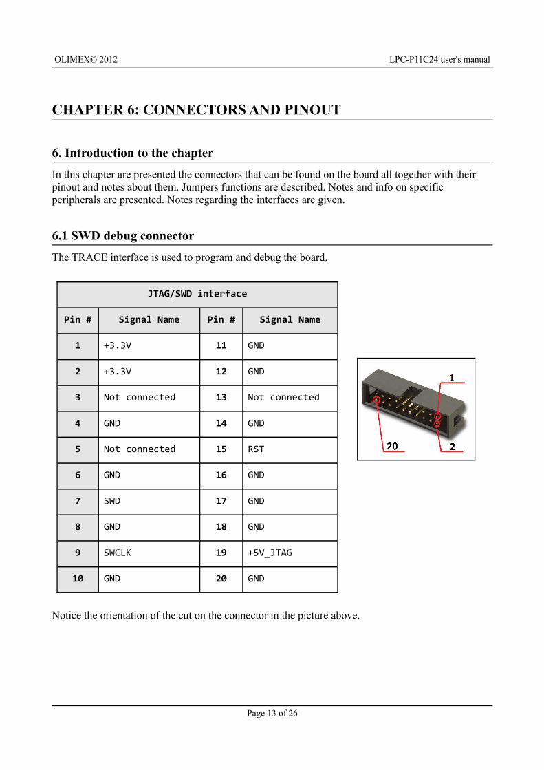
6.1 SWD debug connector
The TRACE interface is used to program and debug the board.
JTAG/SWD interface
Pin # Signal Name Pin # Signal Name
1 +3.3V 11 GND
2 +3.3V 12 GND
3 Not connected 13 Not connected
4 GND 14 GND
5 Not connected 15 RST
6 GND 16 GND
7 SWD 17 GND
8 GND 18 GND
9 SWCLK 19 +5V_JTAG
10 GND 20 GND
Notice the orientation of the cut on the connector in the picture above.
Page 13 of 26
OLIMEX© 2012 LPC-P11C24 user's manual
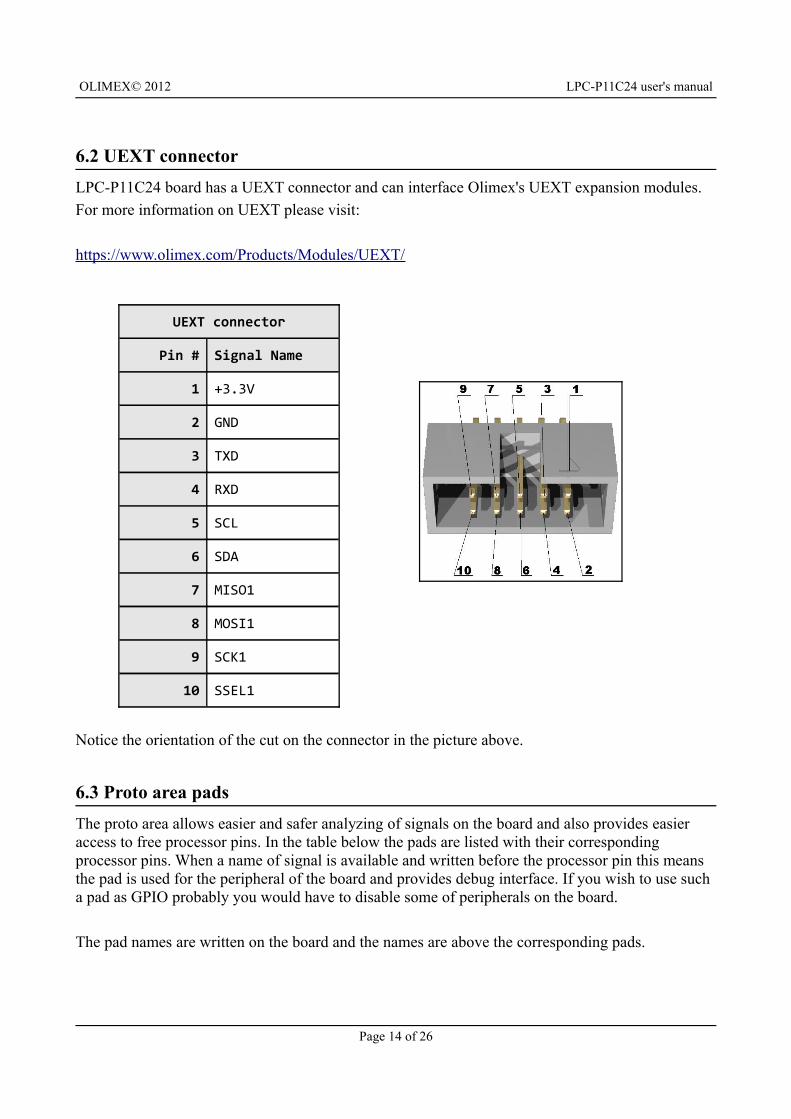
6.2 UEXT connector
LPC-P11C24 board has a UEXT connector and can interface Olimex's UEXT expansion modules.
For more information on UEXT please visit:
https://www.olimex.com/Products/Modules/UEXT/
UEXT connector
Pin # Signal Name
1 +3.3V
2 GND
3 TXD
4 RXD
5 SCL
6 SDA
7 MISO1
8 MOSI1
9 SCK1
10 SSEL1
Notice the orientation of the cut on the connector in the picture above.
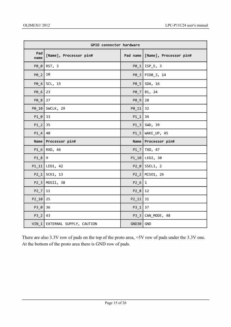
6.3 Proto area pads
The proto area allows easier and safer analyzing of signals on the board and also provides easier access to free processor pins. In the table below the pads are listed with their corresponding processor pins. When a name of signal is available and written before the processor pin this means the pad is used for the peripheral of the board and provides debug interface. If you wish to use such a pad as GPIO probably you would have to disable some of peripherals on the board.
The pad names are written on the board and the names are above the corresponding pads.
Page 14 of 26
OLIMEX© 2012 LPC-P11C24 user's manual
GPIO connector hardware
Pad name
[Name], Processor pin# Pad name [Name], Processor pin#
P0_0 RST, 3 P0_1 ISP_E, 3
P0_2 10 P0_3 PIO0_3, 14
P0_4 SCL, 15 P0_5 SDA, 16
P0_6 23 P0_7 B1, 24
P0_8 27 P0_9 28
P0_10 SWCLK, 29 P0_11 32
P1_0 33 P1_1 34
P1_2 35 P1_3 SWD, 39
P1_4 40 P1_5 WAKE_UP, 45
Name Processor pin# Name Processor pin#
P1_6 RXD, 46 P1_7 TXD, 47
P1_8 9 P1_10 LED2, 30
P1_11 LED1, 42 P2_0 SSEL1, 2
P2_1 SCK1, 13 P2_2 MISO1, 26
P2_3 MOSI1, 38 P2_6 1
P2_7 11 P2_8 12
P2_10 25 P2_11 31
P3_0 36 P3_1 37
P3_2 43 P3_3 CAN_MODE, 48
VIN_1 EXTERNAL SUPPLY, CAUTION GND30 GND
There are also 3.3V row of pads on the top of the proto area, +5V row of pads under the 3.3V one.
At the bottom of the proto area there is GND row of pads.
Page 15 of 26
OLIMEX© 2012 LPC-P11C24 user's manual
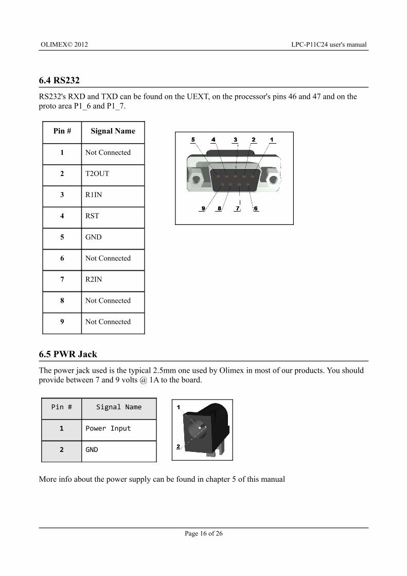
6.4 RS232
RS232's RXD and TXD can be found on the UEXT, on the processor's pins 46 and 47 and on the proto area P1_6 and P1_7.
Pin # Signal Name
1 Not Connected
2 T2OUT
3 R1IN
4 RST
5 GND
6 Not Connected
7 R2IN
8 Not Connected
9 Not Connected
6.5 PWR Jack
The power jack used is the typical 2.5mm one used by Olimex in most of our products. You should provide between 7 and 9 volts @ 1A to the board.
Pin # Signal Name
1 Power Input
2 GND
More info about the power supply can be found in chapter 5 of this manual
Page 16 of 26
OLIMEX© 2012 LPC-P11C24 user's manual
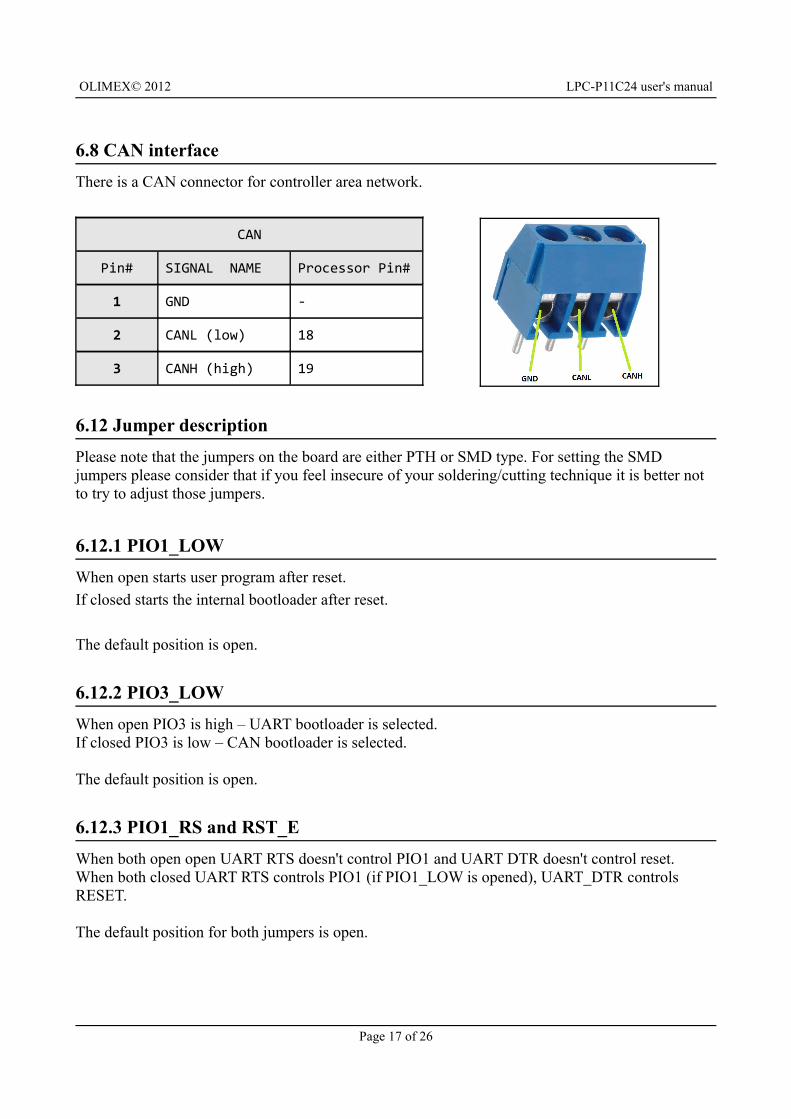
6.8 CAN interface
There is a CAN connector for controller area network.
CAN
Pin# SIGNAL NAME Processor Pin#
1 GND -
2 CANL (low) 18
3 CANH (high) 19
6.12 Jumper description
Please note that the jumpers on the board are either PTH or SMD type. For setting the SMD jumpers please consider that if you feel insecure of your soldering/cutting technique it is better not to try to adjust those jumpers.
6.12.1 PIO1_LOW
When open starts user program after reset.
If closed starts the internal bootloader after reset.
The default position is open.
6.12.2 PIO3_LOW
When open PIO3 is high – UART bootloader is selected.If closed PIO3 is low – CAN bootloader is selected.
The default position is open.
6.12.3 PIO1_RS and RST_E
When both open open UART RTS doesn't control PIO1 and UART DTR doesn't control reset.When both closed UART RTS controls PIO1 (if PIO1_LOW is opened), UART_DTR controls RESET.
The default position for both jumpers is open.
Page 17 of 26
OLIMEX© 2012 LPC-P11C24 user's manual
6.12.4 SILENT/NORMAL
Silent/Normal jumper alternatively switches the CAN operation mode. Either Silent T or Normal T, you need CAN enabled.
The default position is jumper open.
6.12.5 5V_DIS
When open VR2(5V) is enabled.If closed disables VR2(5V).
The default position is open.
6.12.6 CAN_T
When closed CAN terminator (2x62 Ohm) is connected.When open CAN terminator (2x62 Ohm) is disconnected.
The default position is closed.
6.13 Additional hardware components
The components below are mounted on LPC-P11C24 but are not discussed above. They are listed here for completeness:
Reset button - used for hardware reset of the board
B1 and WAKE_UP - buttons
LED1 (Green) + LED2 (Yelow) + Power LED (Red)
Page 18 of 26
OLIMEX© 2012 LPC-P11C24 user's manual
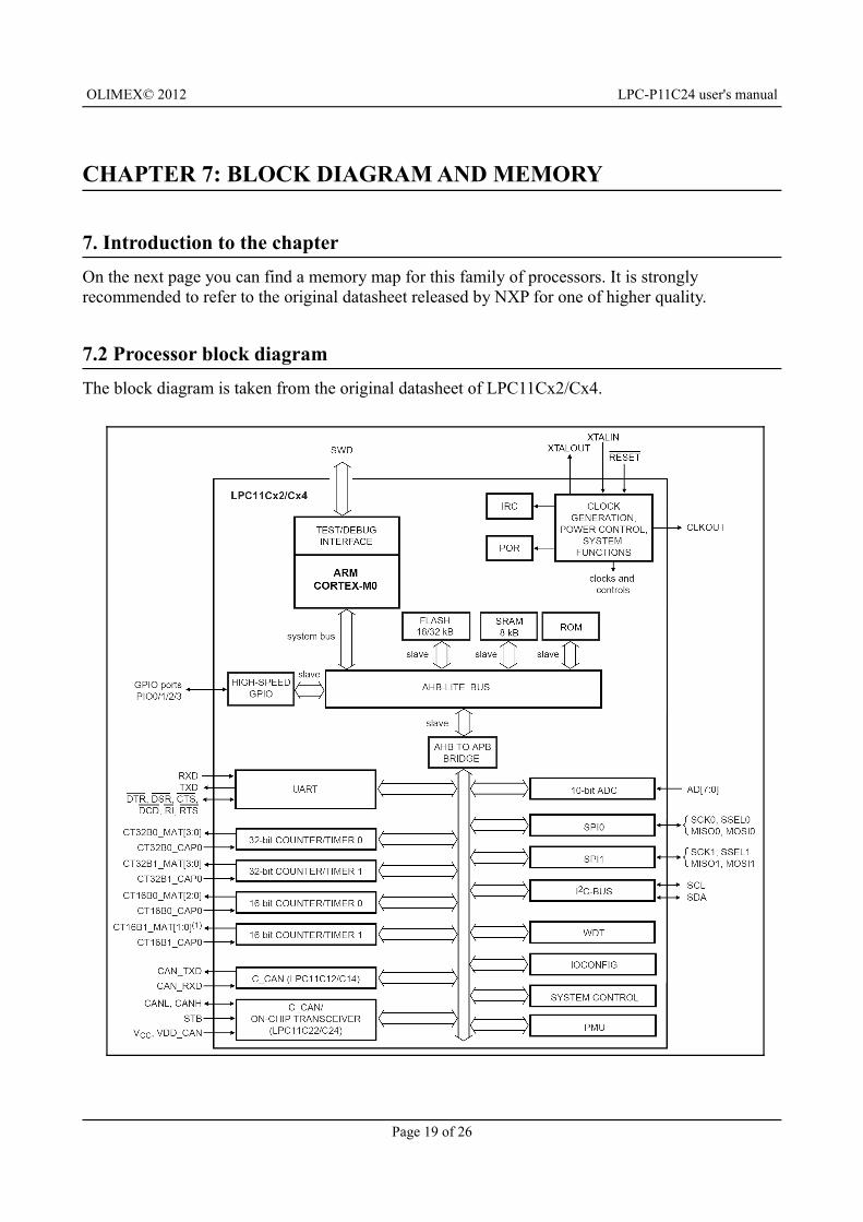
CHAPTER 7: BLOCK DIAGRAM AND MEMORY
7. Introduction to the chapter
On the next page you can find a memory map for this family of processors. It is strongly recommended to refer to the original datasheet released by NXP for one of higher quality.
7.2 Processor block diagram
The block diagram is taken from the original datasheet of LPC11Cx2/Cx4.
Page 19 of 26
OLIMEX© 2012 LPC-P11C24 user's manual
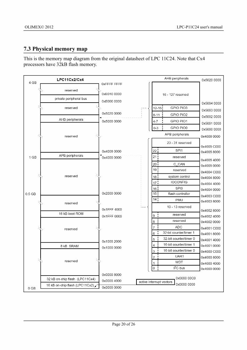
7.3 Physical memory map
This is the memory map diagram from the original datasheet of LPC 11C24. Note that Cx4 processors have 32kB flash memory.
Page 20 of 26
OLIMEX© 2012 LPC-P11C24 user's manual
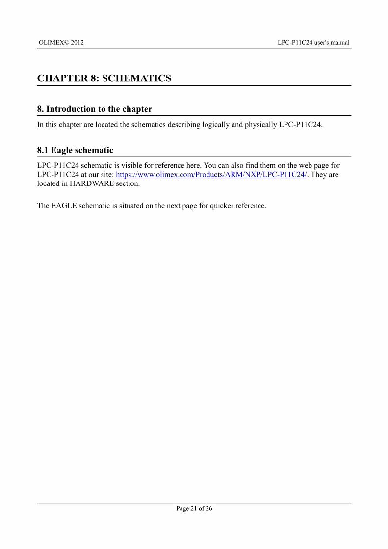
CHAPTER 8: SCHEMATICS
8. Introduction to the chapter
In this chapter are located the schematics describing logically and physically LPC-P11C24.
8.1 Eagle schematic
LPC-P11C24 schematic is visible for reference here. You can also find them on the web page for LPC-P11C24 at our site: https://www.olimex.com/Products/ARM/NXP/LPC-P11C24/. They are located in HARDWARE section.
The EAGLE schematic is situated on the next page for quicker reference.
Page 21 of 26
OLIMEX© 2012 LPC-P11C24 user's manual
Page 22 of 26
T1103NE12x12x4,3
100nF
1nF
10uF/6.3V
10
uF
/6.3
V
100nF 100nF
100nF
10
uF
/16
V/t
an
t
47
0u
F/1
6V
100nF
100nF
18pF
18pF
10uF/6.3V
100nF
100nF
100nF
100nF
100nF
NA
TB3/5MM
clo
se
1N5819S
1N5819S
BAT54A
1N5819S
LED0603/GREENLED0603/YELLOW
VIN
+5V
+5V
+5V
HN1x2
HN1x2
HN1x2
YDJ1136
LED0603/RED
12MHz/20pF
390/1%
240/1%
62R
62R
33k
1K220/1%
22k
1K
22k
1K
680/1%
2K
10k
10k10k10k
22k
2K
2K 2K
1K 1K
22k
1K
1K
1K10k
33
390/1%
T1
10
7A
(6x
3.8
x2
.5m
m)
DB9-female
HN1x2
HN1x3
BH20S
DTC114YKA
LPC11C24FBD48/301
ST3232CDR(SO16)
BH10S
3.3V
3.3V 3.3V
3.3V3.3V
3.3V
3.3V
3.3V
3.3V
3.3V
3.3V
3.3V
3.3V
3.3V
3.3V
LM1117IMPX-ADJLM1117IMPX-ADJ
T1103NE12x12x4,3
BZV55C6V2(NA)
RS
T,S
WC
LK
,SW
O,S
WD
SSEL1,SCK1,MISO1,MOSI1,SCL,SDA,RXD,TXD
+5V
+5V_JTAG
+5V_JTAG
B1
B1
CANH CANHCANL CANL
CAN_MODE
CAN_MODE
ISP_E
ISP_E
LED1
LED1
LED2
LED2MISO1MISO1
MISO1
MOSI1MOSI1
MOSI1
PIO3
RST RST
RST
RST
RST RST
RXD RXD
RXD RXD RXD
SCK1SCK1
SCK1
SCL SCL
SCL
SDA SDA
SDA
SSEL1SSEL1
SSEL1
SWCLK SWCLK
SWCLK SWCLK
SWD SWD
SWDSWD
TXD TXD
TXD TXD
TXD
WAKE_UP
WAKE_UP
+5V
3.3V_1
1 25V_DIS
B1
C1
C4
C5 C6
C7 C8
C9
C11C12
C13
C14
C15
C16
C17
C19
C20
C21
C22
C23
C24
CAN-1
CAN-2
CAN-3
1
2
3
CA
N_
T
D3
D4
D5
D6
GND18GND30
LED1LED2
P0_0P0_1P0_2P0_3P0_4P0_5P0_6P0_7P0_8P0_9P0_10P0_11
P1_0P1_1P1_2P1_3P1_4P1_5P1_6P1_7P1_8P1_10P1_11
P2_0P2_1P2_2P2_3P2_6P2_7P2_8
P2_10P2_11
P3_0P3_1P3_2P3_3
12
PIO1_LOW
12
PIO1_RS
12
PIO3_LOW
PWR
PWR-LED
Q1
R1
R2
R3
R4
R5
R6R7
R8
R9
R10
R11
R12
R13
R18
R19R20R21
R25
R26
R27 R28
R31R34
R43
R44
R45
R47R48
R49
R50
RESET
12345
6789
G1
G2
RS232
1 2
RST_E
1 2 3
SILENT/NORMAL
1234567891011121314151617181920
SWD
T3
#RESET/PIO0_03
CANH19CANL18
GND21
PIO0_1/CLKOUT/CT32B0_MAT24
PIO0_2/SSEL0/CT16B0_CAP010
PIO0_314
PIO0_4/SCL15
PIO0_5/SDA16
PIO0_6/SCK023
PIO0_7/#CTS24
PIO0_8/MISO0/CT16B0_MAT027
PIO0_9/MOSI0/CT16B0_MAT128
PIO1_4/AD5/CT32B1_MAT3/WAKEUP40
PIO1_5/#RTS/CT32B0_CAP045
PIO1_6/RXD/CT32B0_MAT046
PIO1_7/TXD/CT32B0_MAT147
PIO1_8/CT16B1_CAP09
PIO1_10/AD6/CT16B1_MAT130
PIO1_11/AD742
PIO2_0/#DTR/SSEL12
PIO2_1/#DSR/SCK113
PIO2_2/#DCD/MISO126
PIO2_3/#RI/MOSI138
PIO2_61
PIO2_711
PIO2_812
PIO2_1025
PIO2_11/SCK031
PIO3_0/#DTR36
PIO3_1/#DSR37
PIO3_2/#DCD43
PIO3_3/#RI48
R/PIO0_11/AD0/CT32B0_MAT332
R/PIO1_0/AD1/CT32B1_CAP033
R/PIO1_1/AD2/CT32B1_MAT034
R/PIO1_2/AD3/CT32B1_MAT135
STB22
SWCLK/PIO0_10/SCK0/CT16B0_MAT229
SWDIO/PIO1_3/AD4/CT32B1_MAT239
VCC20
VDD8
VDD44
VDD_CAN17
VSS5
VSS41
XTALIN6
XTALOUT7
U2
C1+ 1
C1- 3
C2+ 4
C2- 5
R1IN13 R1OUT 12
R2IN8 R2OUT 9
T1IN 11T1OUT
14
T2IN 10T2OUT
7
V+2
V-6
U3
15 16GND VCC
U3PWR
1 23 45 67 89 10
UEXT
VIN_1
ADJ/GND
IN OUT
VR1(3.3V)
ADJ/GND
IN OUT
VR2(5V)
WAKE_UPZ1
7-9 VDC
LPC-P11C24_rev_A
OLIMEX LTD BULGARIA
http://www.olimex.com/dev
+
10 k
47
k
TRACEDEBUG INTERFACE: BUTTONS
RS232UEXT
LEDS
POWER SUPPLY
+-
OLIMEX© 2012 LPC-P11C24 user's manual
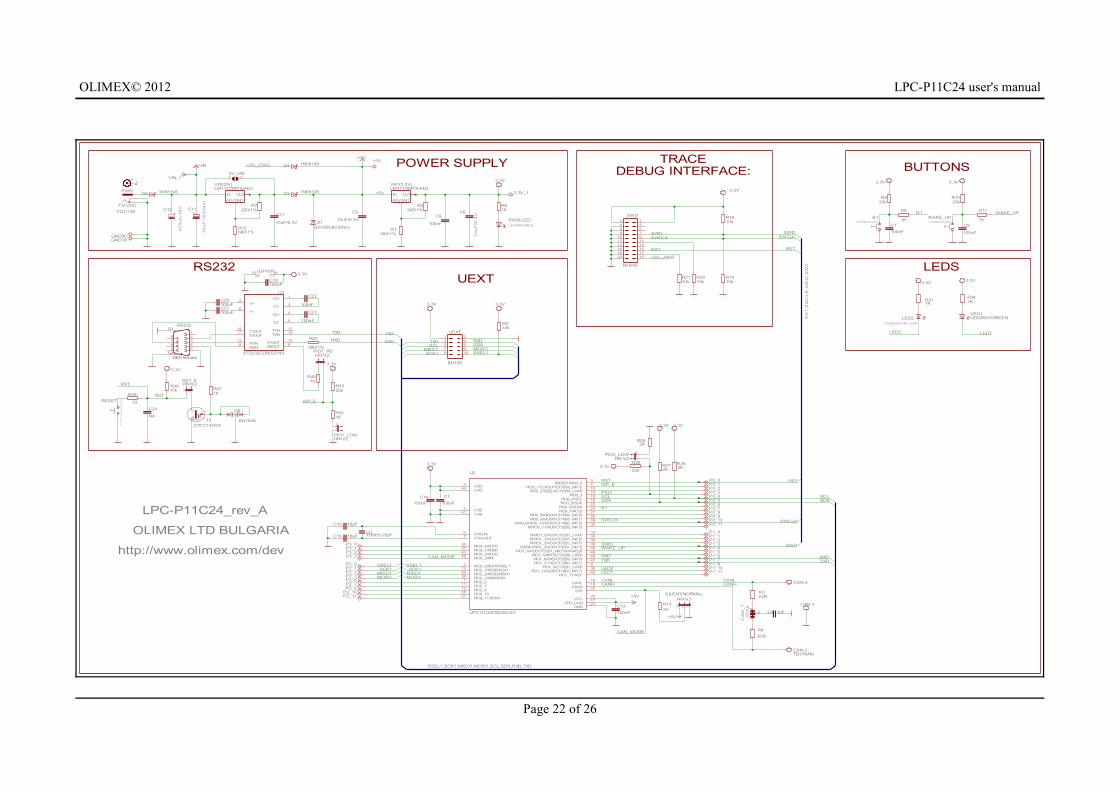
8.2 Physical dimensions
Note that all dimensions are in inches.
The three highest elements on the board in order from the tallest to the shortest are: RS232 connector – 480mil; capacitor C12 – 460mil; Power jack – 420mil.
Page 23 of 26
OLIMEX© 2012 LPC-P11C24 user's manual
CHAPTER 9: REVISION HISTORY AND SUPPORT
9. Introduction to the chapter
In this chapter you will find the current and the previous version of the document you are reading. Also the web-page for your device is listed. Be sure to check it after a purchase for the latest available updates and examples.
9.1 Document revision
Revision Changes Modified Page#
A, 10.07.12 Initial Creation All
B,18.10.12
Added links to each entry in the index table; Fixed and updated various links
4, 21, 25
C,25.03.13
Fixed an error that indicates 6V as sufficient supply voltage; Adjusted formatting; Fixed various links;
7, 8, 12
9.2 Board revision
Revision Notable Changes
A Initial release of the board
Page 24 of 26
OLIMEX© 2012 LPC-P11C24 user's manual
9.3 Useful web links and purchase codes
The web page you can visit for more info on your device is https://www.olimex.com/Products/ARM/NXP/LPC-P11C24/.
ORDER CODES:
LPC-P11C24 – LPC-P11C24 featuring LPC11C24 Cortex-M0 processor
The latest price list can be found at https://www.olimex.com/prices.
How to order?
You can order from our e-shop or via any of our distributors.
Check https://www.olimex.com/ for more info.
Page 25 of 26
OLIMEX© 2012 LPC-P11C24 user's manual
9.3 Product support
For product support, hardware information and error reports mail to: [email protected]. Note that we are primarily a hardware company and our software support is limited.
Please consider reading the paragraph below about the warranty of Olimex products.
Warranty and returns:
Our boards have lifetime warranty against manufacturing defects and components.
During development work it is not unlikely that you can burn your programmer or development board. This is normal, we also do development work and we have damaged A LOT of programmers and boards during our daily job so we know how it works. If our board/programmer has worked fine then stopped, please check if you didn't apply over voltage by mistake, or shorted something in your target board where the programmer was connected etc. Sometimes boards might get damaged by ESD shock voltage or if you spill coffee on them during your work when they are powered.
Please note that warrany do not cover problems caused by unproper use, shorts, over-voltages, ESD shock etc.
If the board has warranty label it should be not broken. Broken labels void the warranty, same applies for boards modified by the customer, for instance soldering additional components or removing components - such boards will be not be a subject of our warranty.
If you are positive that the problem is due to manufacturing defect or component you can return the board back to us for inspection.
When we receive the board we will check and if the problem is caused due to our fault and we will repair/replace the faulty hardware free of charge, otherwise we can quote price of the repair.
Note that all shippings back and forth have to be covered by the customer. Before you ship anything back you need to ask for RMA. When you ship back please attach to it your shipping address, phone, e-mail, RMA# and brief description of the problem. All boards should be sent back in antistatic package and well packed to prevent damages during the transport.
Page 26 of 26


![Chapter 1 · Linear Prediction Coding (LPC)[10], LPC-derived Cepstrum (LPCC)[11], Mel Frequency Cepstrum Coefficient (MFCC)[12], and Perceptual Linear Predictive analysis (PLP)[13],](https://static.fdocuments.us/doc/165x107/5ebf8e7c34062f242163c649/chapter-1-linear-prediction-coding-lpc10-lpc-derived-cepstrum-lpcc11-mel.jpg)