LP8752xQ1EVM Evaluation Module (Rev. A) - Texas … Evaluation Module 2.1 Installing/Opening the...
45
1 SNVU508A – October 2016 – Revised February 2017 Submit Documentation Feedback Copyright © 2016–2017, Texas Instruments Incorporated LP8752xQ1EVM Evaluation Module User's Guide SNVU508A – October 2016 – Revised February 2017 LP8752xQ1EVM Evaluation Module This user’s guide describes the operation of the evaluation module for the LP8752xQ1 multi-phase 4-core step-down converter from Texas Instruments (TI). The LP8752xQ1 can be used in five different output configurations, and this user’s guide includes all these five variants (see Table 1). The user’s guide also provides design information, including the schematic and bill of materials (BOM). Contents 1 Overview ...................................................................................................................... 3 2 Quick Setup Guide........................................................................................................... 3 2.1 Installing/Opening the Software .................................................................................. 4 2.2 Power Supply Setup ................................................................................................ 8 2.3 Notes on Efficiency Measurement Procedure ................................................................. 11 3 GUI Overview ............................................................................................................... 11 3.1 Main Tab ........................................................................................................... 11 3.2 Other Tabs and Menus ........................................................................................... 12 3.3 Console ............................................................................................................. 18 4 Bill of Materials ............................................................................................................. 20 5 Board Layout ................................................................................................................ 22 6 LP8752xQ1EVM Schematics ............................................................................................. 29 List of Figures 1 LP8752xQ1EVM ............................................................................................................. 3 2 LP8752 Installer License Agreement...................................................................................... 4 3 Features of LP8752 Installation............................................................................................ 5 4 LP8752 Destination Folder ................................................................................................. 5 5 LP8752 Installation Complete .............................................................................................. 6 6 Evaluation Software Graphical User Interface (GUI) When Board Connected ...................................... 7 7 Assert nRST .................................................................................................................. 9 8 Read Registers -buttons. ................................................................................................... 9 9 BUCK0, BUCK1, BUCK2 and BUCK3 Enabled ........................................................................ 10 10 Assert EN1 .................................................................................................................. 10 11 Accessing Direct Register Write.......................................................................................... 13 12 Direct Register Access View.............................................................................................. 14 13 Selecting Register Values................................................................................................. 15 14 Register Update Mode..................................................................................................... 16 15 Config Tab of the LP8752xQ1 GUI ...................................................................................... 17 16 Advanced Tab of LP8752 GUI ........................................................................................... 17 17 Opening Console ........................................................................................................... 18
Transcript of LP8752xQ1EVM Evaluation Module (Rev. A) - Texas … Evaluation Module 2.1 Installing/Opening the...
1SNVU508A–October 2016–Revised February 2017Submit Documentation Feedback
Copyright © 2016–2017, Texas Instruments Incorporated
LP8752xQ1EVM Evaluation Module
User's GuideSNVU508A–October 2016–Revised February 2017
LP8752xQ1EVM Evaluation Module
This user’s guide describes the operation of the evaluation module for the LP8752xQ1 multi-phase 4-corestep-down converter from Texas Instruments (TI). The LP8752xQ1 can be used in five different outputconfigurations, and this user’s guide includes all these five variants (see Table 1). The user’s guide alsoprovides design information, including the schematic and bill of materials (BOM).
Contents1 Overview ...................................................................................................................... 32 Quick Setup Guide........................................................................................................... 3
2.1 Installing/Opening the Software .................................................................................. 42.2 Power Supply Setup................................................................................................ 82.3 Notes on Efficiency Measurement Procedure ................................................................. 11
3 GUI Overview ............................................................................................................... 113.1 Main Tab ........................................................................................................... 113.2 Other Tabs and Menus ........................................................................................... 123.3 Console ............................................................................................................. 18
4 Bill of Materials ............................................................................................................. 205 Board Layout................................................................................................................ 226 LP8752xQ1EVM Schematics ............................................................................................. 29
List of Figures
1 LP8752xQ1EVM ............................................................................................................. 32 LP8752 Installer License Agreement...................................................................................... 43 Features of LP8752 Installation............................................................................................ 54 LP8752 Destination Folder ................................................................................................. 55 LP8752 Installation Complete .............................................................................................. 66 Evaluation Software Graphical User Interface (GUI) When Board Connected ...................................... 77 Assert nRST .................................................................................................................. 98 Read Registers -buttons. ................................................................................................... 99 BUCK0, BUCK1, BUCK2 and BUCK3 Enabled........................................................................ 1010 Assert EN1 .................................................................................................................. 1011 Accessing Direct Register Write.......................................................................................... 1312 Direct Register Access View.............................................................................................. 1413 Selecting Register Values................................................................................................. 1514 Register Update Mode..................................................................................................... 1615 Config Tab of the LP8752xQ1 GUI ...................................................................................... 1716 Advanced Tab of LP8752 GUI ........................................................................................... 1717 Opening Console........................................................................................................... 18
www.ti.com
2 SNVU508A–October 2016–Revised February 2017Submit Documentation Feedback
Copyright © 2016–2017, Texas Instruments Incorporated
LP8752xQ1EVM Evaluation Module
18 Example of Command Use in Console.................................................................................. 1919 Board Stack-Up............................................................................................................. 2220 Top View of the LP8752xQ1EVM ........................................................................................ 2321 Component Placement on Top Layer ................................................................................... 2322 Component Placement on Bottom Layer ............................................................................... 2423 Top Layer ................................................................................................................... 2524 Mid-Layer1 ................................................................................................................. 2525 Mid-Layer2 .................................................................................................................. 2626 Mid-Layer3 .................................................................................................................. 2627 Mid-Layer4, GND Plane ................................................................................................... 2728 Bottom Layer (note mirror view).......................................................................................... 2729 LP87521Q1EVM Schematic .............................................................................................. 2930 LP87522Q1EVM Schematic .............................................................................................. 3031 LP87523Q1EVM Schematic .............................................................................................. 3132 LP87524Q1EVM Schematic .............................................................................................. 3233 LP87525Q1EVM Schematic .............................................................................................. 3334 EVM Connectors ........................................................................................................... 3435 EVM I2C Interface .......................................................................................................... 35
List of Tables
1 LP8752xQ1 Configurations................................................................................................. 32 Mode Information........................................................................................................... 123 I2C-Compatible Bus Support .............................................................................................. 124 Console Macros ............................................................................................................ 195 Bill of Materials or LP8752xQ1EVM ..................................................................................... 20
TrademarksAll trademarks are the property of their respective owners.
www.ti.com Overview
3SNVU508A–October 2016–Revised February 2017Submit Documentation Feedback
Copyright © 2016–2017, Texas Instruments Incorporated
LP8752xQ1EVM Evaluation Module
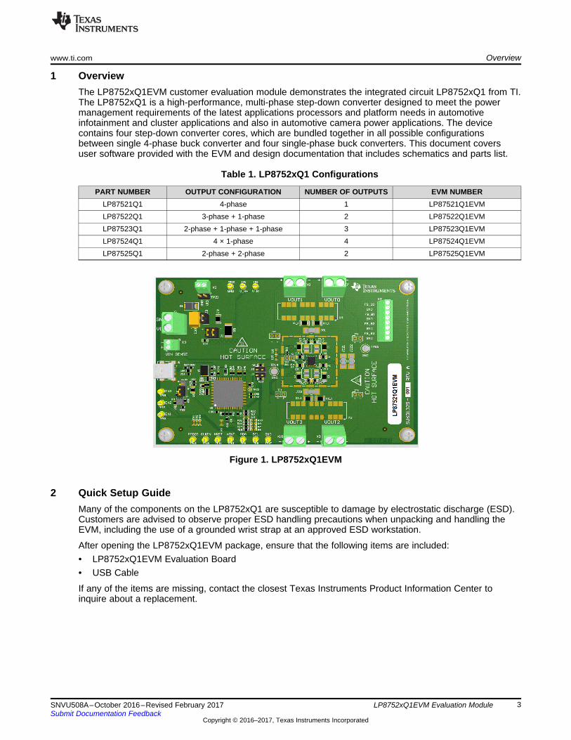
1 OverviewThe LP8752xQ1EVM customer evaluation module demonstrates the integrated circuit LP8752xQ1 from TI.The LP8752xQ1 is a high-performance, multi-phase step-down converter designed to meet the powermanagement requirements of the latest applications processors and platform needs in automotiveinfotainment and cluster applications and also in automotive camera power applications. The devicecontains four step-down converter cores, which are bundled together in all possible configurationsbetween single 4-phase buck converter and four single-phase buck converters. This document coversuser software provided with the EVM and design documentation that includes schematics and parts list.
Table 1. LP8752xQ1 Configurations
PART NUMBER OUTPUT CONFIGURATION NUMBER OF OUTPUTS EVM NUMBERLP87521Q1 4-phase 1 LP87521Q1EVMLP87522Q1 3-phase + 1-phase 2 LP87522Q1EVMLP87523Q1 2-phase + 1-phase + 1-phase 3 LP87523Q1EVMLP87524Q1 4 × 1-phase 4 LP87524Q1EVMLP87525Q1 2-phase + 2-phase 2 LP87525Q1EVM
Figure 1. LP8752xQ1EVM
2 Quick Setup GuideMany of the components on the LP8752xQ1 are susceptible to damage by electrostatic discharge (ESD).Customers are advised to observe proper ESD handling precautions when unpacking and handling theEVM, including the use of a grounded wrist strap at an approved ESD workstation.
After opening the LP8752xQ1EVM package, ensure that the following items are included:• LP8752xQ1EVM Evaluation Board• USB Cable
If any of the items are missing, contact the closest Texas Instruments Product Information Center toinquire about a replacement.
Quick Setup Guide www.ti.com
4 SNVU508A–October 2016–Revised February 2017Submit Documentation Feedback
Copyright © 2016–2017, Texas Instruments Incorporated
LP8752xQ1EVM Evaluation Module
2.1 Installing/Opening the SoftwareThe EVM software is controlled through a graphical user interface (GUI). The software communicates withthe EVM through an available USB port. The minimum hardware requirements for the EVM software are:• IBM PC-compatible computer running a Microsoft Windows® XP or newer operating system• Available USB port• Mouse
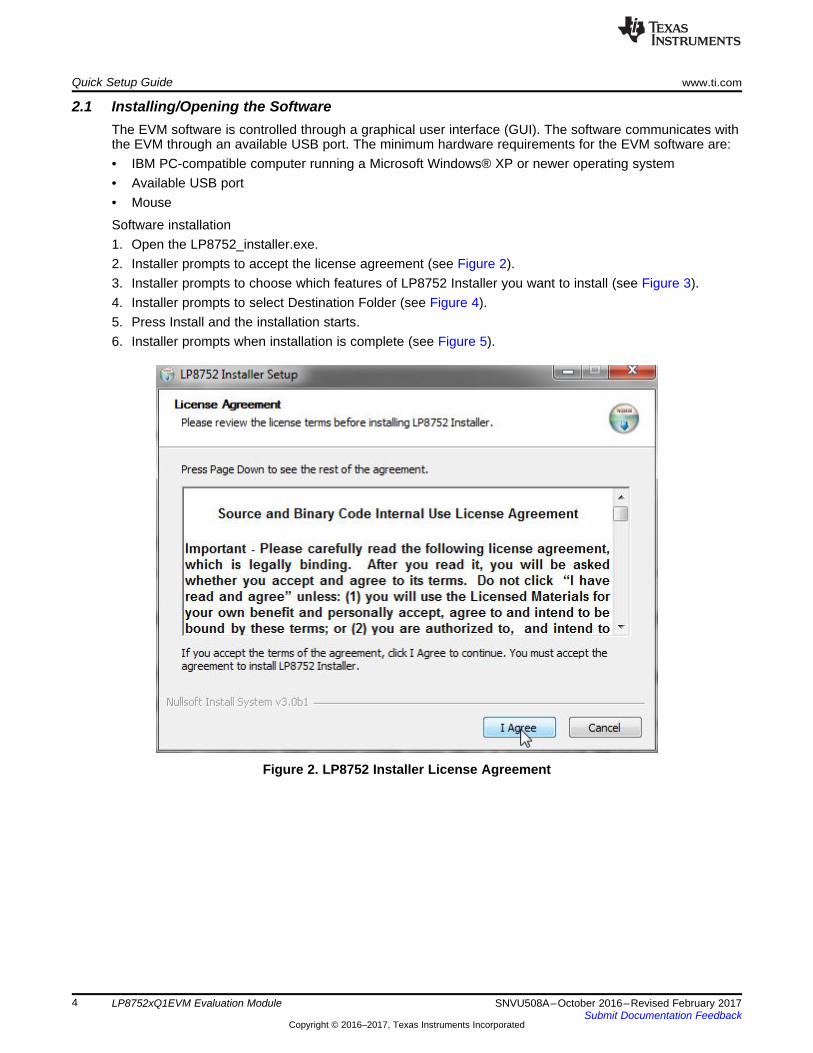
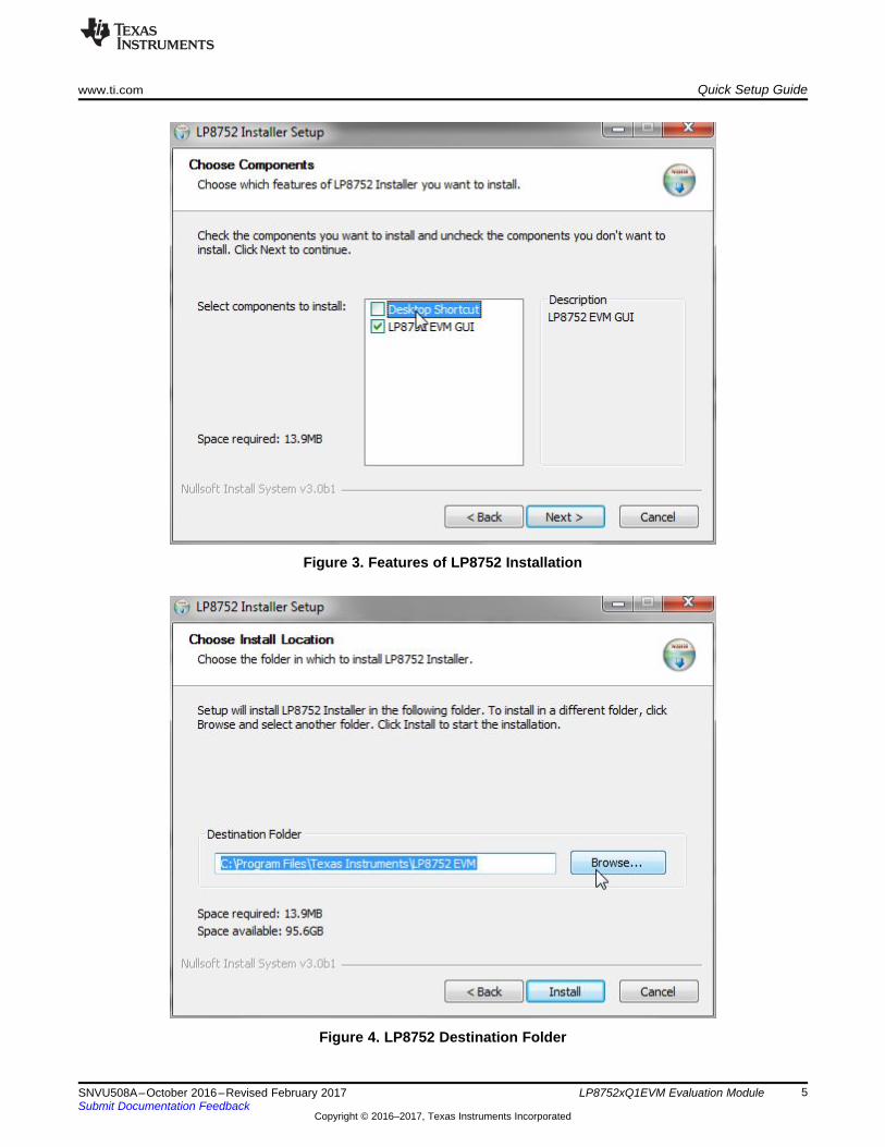
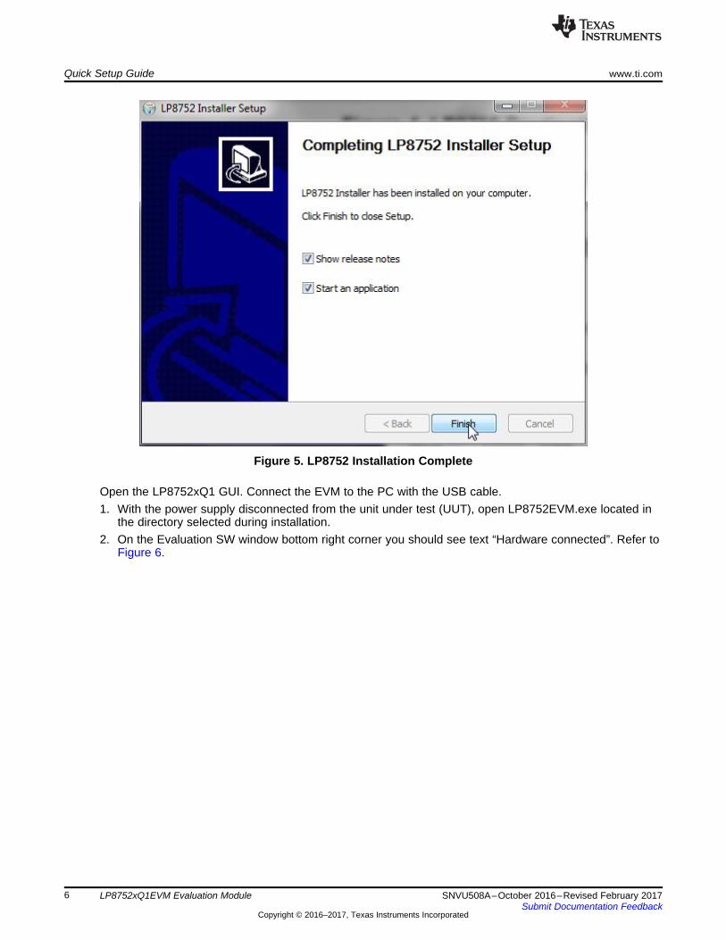
Software installation1. Open the LP8752_installer.exe.2. Installer prompts to accept the license agreement (see Figure 2).3. Installer prompts to choose which features of LP8752 Installer you want to install (see Figure 3).4. Installer prompts to select Destination Folder (see Figure 4).5. Press Install and the installation starts.6. Installer prompts when installation is complete (see Figure 5).
Figure 2. LP8752 Installer License Agreement
www.ti.com Quick Setup Guide
5SNVU508A–October 2016–Revised February 2017Submit Documentation Feedback
Copyright © 2016–2017, Texas Instruments Incorporated
LP8752xQ1EVM Evaluation Module
Figure 3. Features of LP8752 Installation
Figure 4. LP8752 Destination Folder
Quick Setup Guide www.ti.com
6 SNVU508A–October 2016–Revised February 2017Submit Documentation Feedback
Copyright © 2016–2017, Texas Instruments Incorporated
LP8752xQ1EVM Evaluation Module
Figure 5. LP8752 Installation Complete
Open the LP8752xQ1 GUI. Connect the EVM to the PC with the USB cable.1. With the power supply disconnected from the unit under test (UUT), open LP8752EVM.exe located in
the directory selected during installation.2. On the Evaluation SW window bottom right corner you should see text “Hardware connected”. Refer to
Figure 6.
www.ti.com Quick Setup Guide
7SNVU508A–October 2016–Revised February 2017Submit Documentation Feedback
Copyright © 2016–2017, Texas Instruments Incorporated
LP8752xQ1EVM Evaluation Module
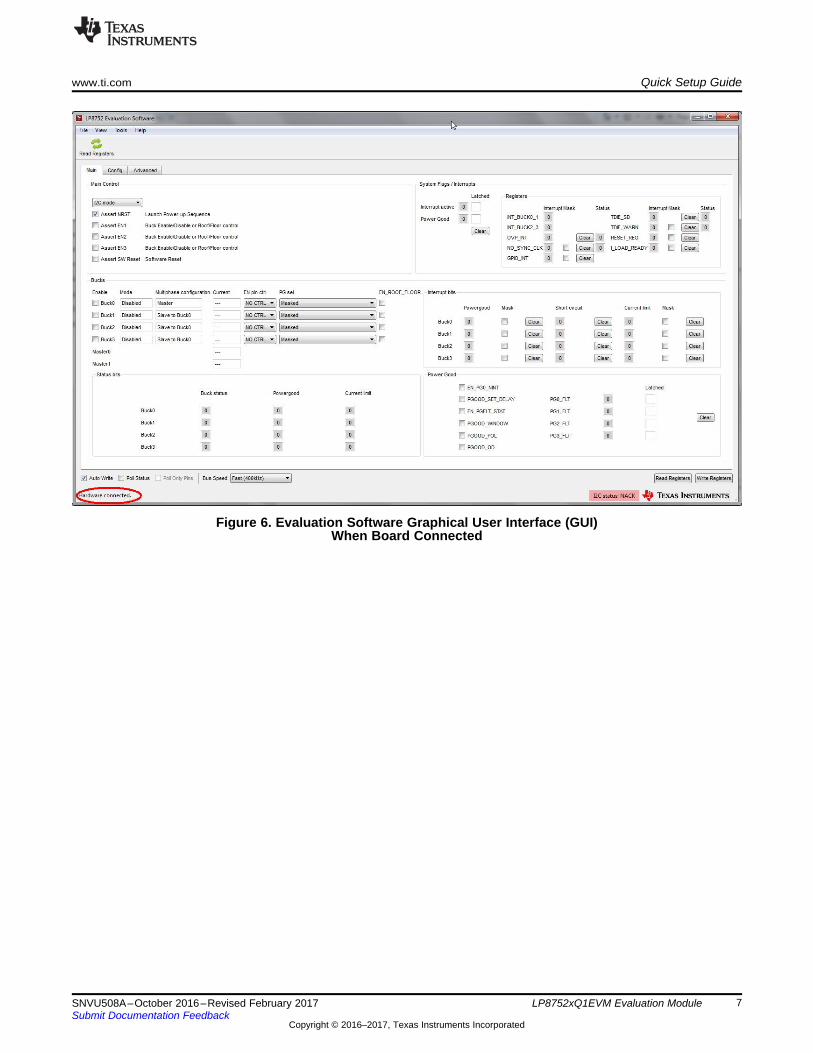
Figure 6. Evaluation Software Graphical User Interface (GUI)When Board Connected
Quick Setup Guide www.ti.com
8 SNVU508A–October 2016–Revised February 2017Submit Documentation Feedback
Copyright © 2016–2017, Texas Instruments Incorporated
LP8752xQ1EVM Evaluation Module
2.2 Power Supply SetupTo power up the EVM, one power supply is needed. For full-load testing of the LP8752xQ1EVM, a DC-power supply capable of at least 5 A and 4 V is required. The power supply is connected to the EVMusing connector X1. The power supply and cabling must present low impedance to the UUT; the length ofpower supply cables must be minimized. Remote sense, using connector X3, can be used to compensatefor voltage drops in the cabling.
With the power supply disconnected from the UUT, set the supply to 3.7 V DC and the current limit to 5 Aminimum. Set the power supply output OFF. Connect the power supply's positive terminal (+) to VIN andnegative terminal (–) to GND on UUT (X1 power-in terminal block). Check that jumpers on the boards areset as shown in Figure 1 (factory default jumper configuration).
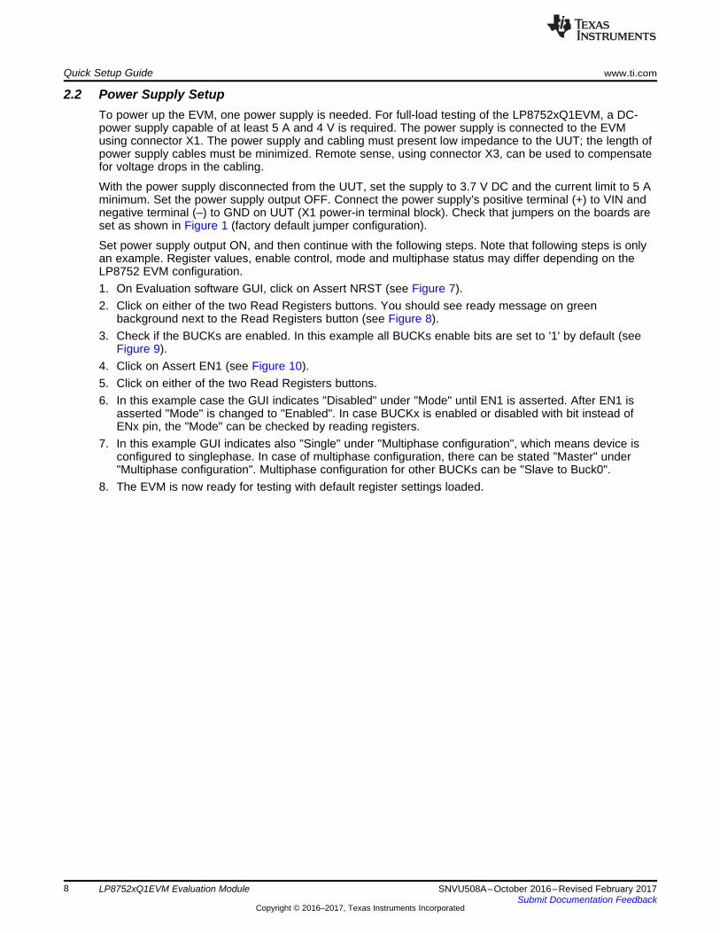
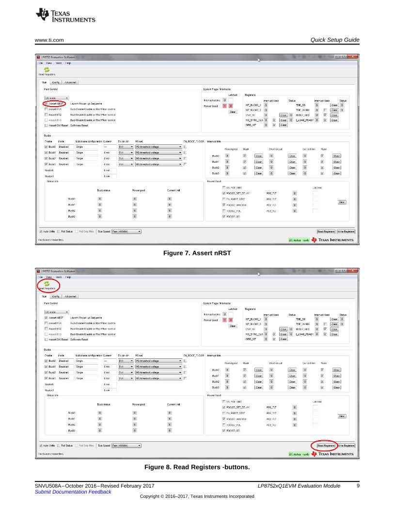
Set power supply output ON, and then continue with the following steps. Note that following steps is onlyan example. Register values, enable control, mode and multiphase status may differ depending on theLP8752 EVM configuration.1. On Evaluation software GUI, click on Assert NRST (see Figure 7).2. Click on either of the two Read Registers buttons. You should see ready message on green
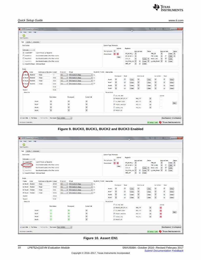
background next to the Read Registers button (see Figure 8).3. Check if the BUCKs are enabled. In this example all BUCKs enable bits are set to '1' by default (see
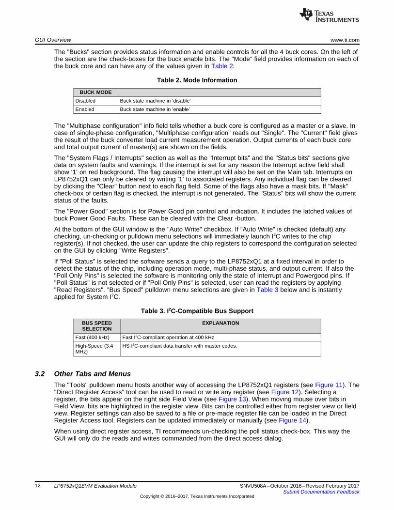
Figure 9).4. Click on Assert EN1 (see Figure 10).5. Click on either of the two Read Registers buttons.6. In this example case the GUI indicates "Disabled" under "Mode" until EN1 is asserted. After EN1 is
asserted "Mode" is changed to "Enabled". In case BUCKx is enabled or disabled with bit instead ofENx pin, the "Mode" can be checked by reading registers.
7. In this example GUI indicates also "Single" under "Multiphase configuration", which means device isconfigured to singlephase. In case of multiphase configuration, there can be stated "Master" under"Multiphase configuration". Multiphase configuration for other BUCKs can be "Slave to Buck0".
8. The EVM is now ready for testing with default register settings loaded.
www.ti.com Quick Setup Guide
9SNVU508A–October 2016–Revised February 2017Submit Documentation Feedback
Copyright © 2016–2017, Texas Instruments Incorporated
LP8752xQ1EVM Evaluation Module
Figure 7. Assert nRST
Figure 8. Read Registers -buttons.
Quick Setup Guide www.ti.com
10 SNVU508A–October 2016–Revised February 2017Submit Documentation Feedback
Copyright © 2016–2017, Texas Instruments Incorporated
LP8752xQ1EVM Evaluation Module
Figure 9. BUCK0, BUCK1, BUCK2 and BUCK3 Enabled
Figure 10. Assert EN1

www.ti.com Quick Setup Guide
11SNVU508A–October 2016–Revised February 2017Submit Documentation Feedback
Copyright © 2016–2017, Texas Instruments Incorporated
LP8752xQ1EVM Evaluation Module
2.3 Notes on Efficiency Measurement ProcedureOutput Connections: An appropriate electronic load or high-power system source meter instrument,specified for operation down to 500 mV, is desirable for loading the UUT. The maximum load current isspecified as 10 A for all phases. Be sure to choose the correct wire size when attaching the electronicload. A wire resistance that is too high will cause a voltage drop in the power distribution path whichbecomes significant compared to the absolute value of the output voltage. Connect an electric load to X7,X8, X9 and/or X10. It is advised that, prior to connecting the load, it be set to sink 0 A to avoid powersurges or possible shocks.
Voltage drop across the PCB traces will yield inaccurate efficiency measurements. For the most accuratevoltage measurement at the EVM, use TP7 to measure the input voltage and X2 to measure the outputvoltage.
To measure the current flowing to/from the UUT, use the current meter of the DC power supply/electricload as long as it is accurate. Some power source ammeters may show offset of several milliamps, andthus will yield inaccurate efficiency measurements. In order to perform very accurate IQ measurements onthe UUT, disconnect input protective Zener diode D1 by removing the shunt J3 from the board. Whenconnected, this diode will cause some leakage, especially on high VIN voltages.
3 GUI OverviewThe evaluation software has the following tabs: Main, Config, and Advanced. The three tabs togetherprovide the user access to the whole register map of LP8752xQ1. Additional register control can beobtained from Tools --> Direct Register Access.
3.1 Main TabThe Main tab (see for example Figure 10) has the elemental controls for the EVM and provides a view tothe chip status. Starting from top, the main controls are:• I2C mode or 4 Enable mode. If this states I2C mode, device is controlled with I2C. When this states
4EN mode, bucks are controlled with ENx pins.• Assert NRST: This checkbox will assert high level to LP8752xQ1 NRST pin. This pin enables the chip
internal voltage reference and bias circuitry.• Assert EN1: This checkbox will assert high level to LP8752xQ1 EN1 pin. Asserting EN1 may enable
the buck regulator(s) or switch to different output voltage level, depending on the register settings.• Assert EN2: This checkbox will assert high level to LP8752xQ1 EN2 pin. Asserting EN2 may enable
the buck regulator(s) or switch to different output voltage level, depending on the register settings.• Assert EN3: This checkbox will assert high level to LP8752xQ1 EN3 pin. Asserting EN3 may enable
the buck regulator(s) or switch to different output voltage level, depending on the register settings.• Assert EN4: In 4 Enable mode, this checkbox will assert high level to LP8752xQ1 SCL pin (alternative
function is EN4). Asserting EN4 may enable the buck regulator(s), depending on the register settings.This checkbox is visible only when device is configured to 4 Enable signal mode.
• Assert SW Reset: To perform a complete SW reset to the chip, assert this checkbox. See the LP8752data sheet for explanation of LP8752xQ1 reset scenarios.
NOTE: The recommended start-up sequence for LP8752xQ1 is to first assert NRST, then write allneeded configuration bits by using the GUI, and then enable buck regulator(s) by ENx pin orEN_BUCKx bit.
GUI Overview www.ti.com
12 SNVU508A–October 2016–Revised February 2017Submit Documentation Feedback
Copyright © 2016–2017, Texas Instruments Incorporated
LP8752xQ1EVM Evaluation Module
The "Bucks" section provides status information and enable controls for all the 4 buck cores. On the left ofthe section are the check-boxes for the buck enable bits. The "Mode" field provides information on each ofthe buck core and can have any of the values given in Table 2:
Table 2. Mode Information
BUCK MODEDisabled Buck state machine in 'disable'Enabled Buck state machine in 'enable'
The "Multiphase configuration" info field tells whether a buck core is configured as a master or a slave. Incase of single-phase configuration, "Multiphase configuration" reads out "Single". The "Current" field givesthe result of the buck converter load current measurement operation. Output currents of each buck coreand total output current of master(s) are shown on the fields.
The "System Flags / Interrupts" section as well as the "Interrupt bits" and the "Status bits" sections givedata on system faults and warnings. If the interrupt is set for any reason the Interrupt active field shallshow ‘1’ on red background. The flag causing the interrupt will also be set on the Main tab. Interrupts onLP8752xQ1 can only be cleared by writing '1’ to associated registers. Any individual flag can be clearedby clicking the "Clear" button next to each flag field. Some of the flags also have a mask bits. If "Mask"check-box of certain flag is checked, the interrupt is not generated. The "Status" bits will show the currentstatus of the faults.
The "Power Good" section is for Power Good pin control and indication. It includes the latched values ofbuck Power Good Faults. These can be cleared with the Clear -button.
At the bottom of the GUI window is the "Auto Write" checkbox. If "Auto Write" is checked (default) anychecking, un-checking or pulldown menu selections will immediately launch I2C writes to the chipregister(s). If not checked, the user can update the chip registers to correspond the configuration selectedon the GUI by clicking "Write Registers".
If "Poll Status" is selected the software sends a query to the LP8752xQ1 at a fixed interval in order todetect the status of the chip, including operation mode, multi-phase status, and output current. If also the"Poll Only Pins" is selected the software is monitoring only the state of Interrupt and Powergood pins. If"Poll Status" is not selected or if "Poll Only Pins" is selected, user can read the registers by applying"Read Registers". "Bus Speed" pulldown menu selections are given in Table 3 below and is instantlyapplied for System I2C.
Table 3. I2C-Compatible Bus Support
BUS SPEEDSELECTION
EXPLANATION
Fast (400 kHz) Fast I2C-compliant operation at 400 kHzHigh-Speed (3.4MHz)
HS I2C-compliant data transfer with master codes.
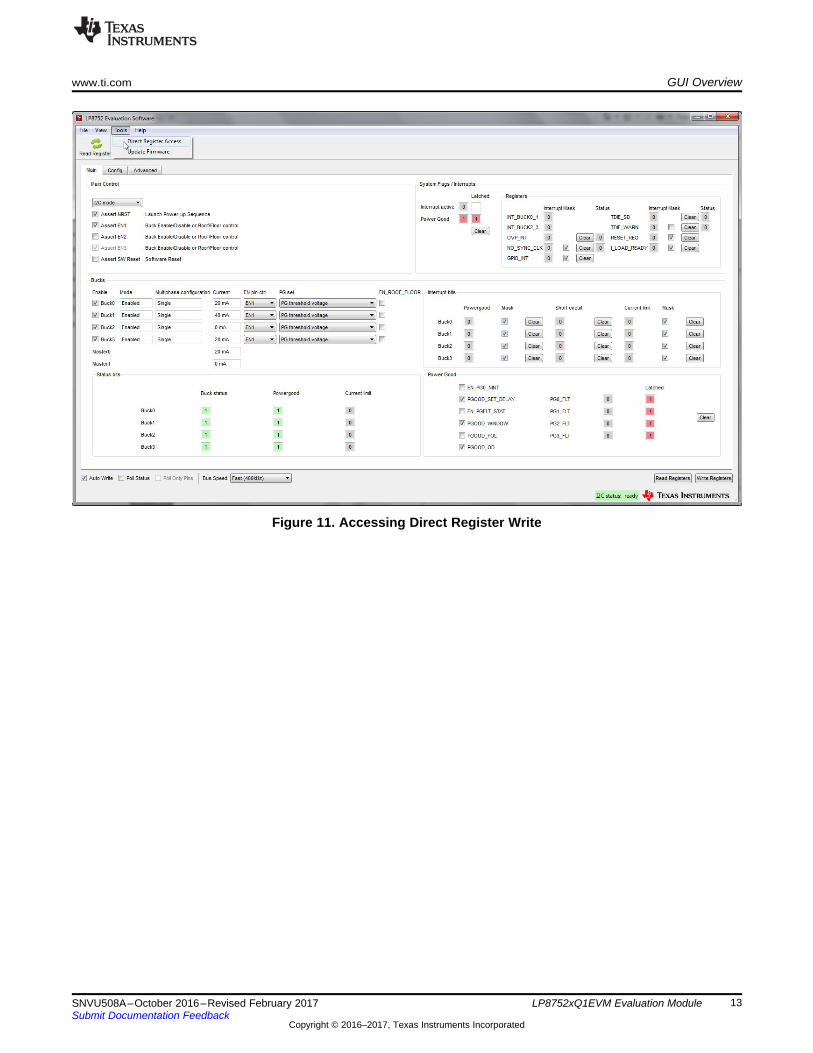
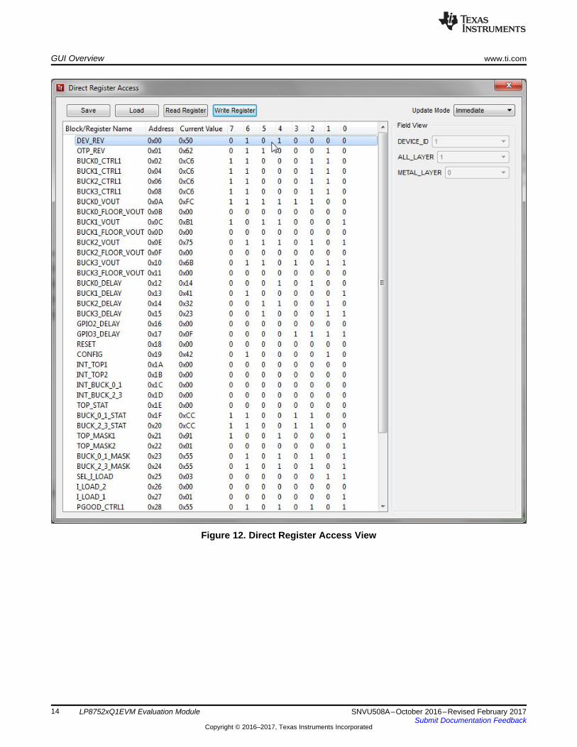
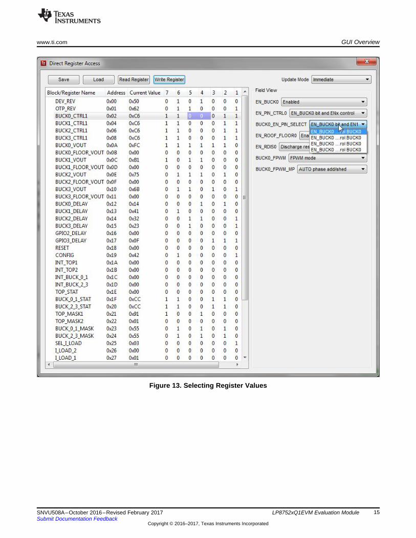
3.2 Other Tabs and MenusThe "Tools" pulldown menu hosts another way of accessing the LP8752xQ1 registers (see Figure 11). The"Direct Register Access" tool can be used to read or write any register (see Figure 12). Selecting aregister, the bits appear on the right side Field View (see Figure 13). When moving mouse over bits inField View, bits are highlighted in the register view. Bits can be controlled either from register view or fieldview. Register settings can also be saved to a file or pre-made register file can be loaded in the DirectRegister Access tool. Registers can be updated immediately or manually (see Figure 14).
When using direct register access, TI recommends un-checking the poll status check-box. This way theGUI will only do the reads and writes commanded from the direct access dialog.
www.ti.com GUI Overview
13SNVU508A–October 2016–Revised February 2017Submit Documentation Feedback
Copyright © 2016–2017, Texas Instruments Incorporated
LP8752xQ1EVM Evaluation Module
Figure 11. Accessing Direct Register Write
GUI Overview www.ti.com
14 SNVU508A–October 2016–Revised February 2017Submit Documentation Feedback
Copyright © 2016–2017, Texas Instruments Incorporated
LP8752xQ1EVM Evaluation Module
Figure 12. Direct Register Access View
www.ti.com GUI Overview
15SNVU508A–October 2016–Revised February 2017Submit Documentation Feedback
Copyright © 2016–2017, Texas Instruments Incorporated
LP8752xQ1EVM Evaluation Module
Figure 13. Selecting Register Values

GUI Overview www.ti.com
16 SNVU508A–October 2016–Revised February 2017Submit Documentation Feedback
Copyright © 2016–2017, Texas Instruments Incorporated
LP8752xQ1EVM Evaluation Module
Figure 14. Register Update Mode
The "Config" and "Advanced" tabs provide the user with pulldown menus and check-boxes for the part ofthe register space that is not covered by the Main tab, such as output voltage control. These controls areself-explanatory. Please refer to the LP8752xQ1 data sheet for explanation of the functions. See followingimages for reference of the Config and Advanced tabs.

www.ti.com GUI Overview
17SNVU508A–October 2016–Revised February 2017Submit Documentation Feedback
Copyright © 2016–2017, Texas Instruments Incorporated
LP8752xQ1EVM Evaluation Module
Figure 15. Config Tab of the LP8752xQ1 GUI
Figure 16. Advanced Tab of LP8752 GUI
GUI Overview www.ti.com
18 SNVU508A–October 2016–Revised February 2017Submit Documentation Feedback
Copyright © 2016–2017, Texas Instruments Incorporated
LP8752xQ1EVM Evaluation Module
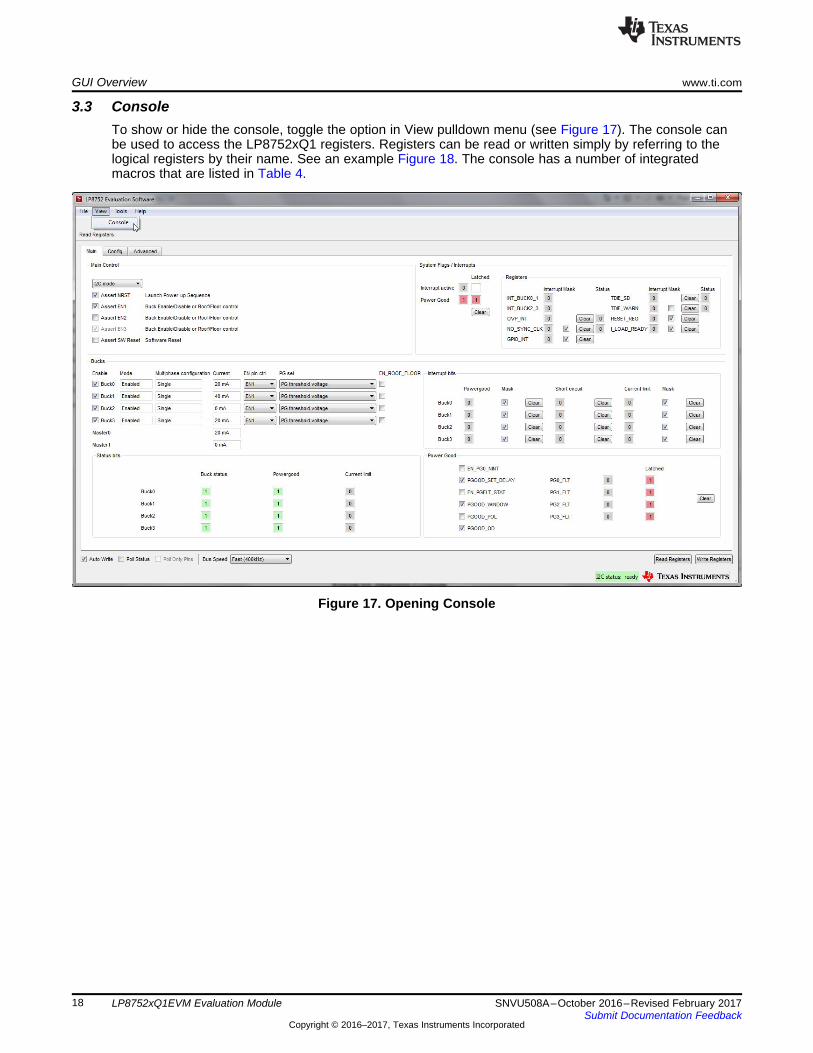
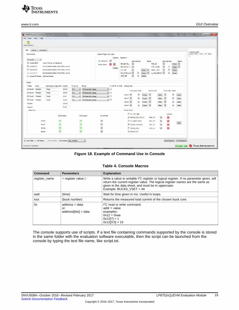
3.3 ConsoleTo show or hide the console, toggle the option in View pulldown menu (see Figure 17). The console canbe used to access the LP8752xQ1 registers. Registers can be read or written simply by referring to thelogical registers by their name. See an example Figure 18. The console has a number of integratedmacros that are listed in Table 4.
Figure 17. Opening Console
www.ti.com GUI Overview
19SNVU508A–October 2016–Revised February 2017Submit Documentation Feedback
Copyright © 2016–2017, Texas Instruments Incorporated
LP8752xQ1EVM Evaluation Module
Figure 18. Example of Command Use in Console
Table 4. Console Macros
Command Parameters Explanationregister_name = register value | - Write a value to writable I2C register or logical register. If no parameter given, will
return the current register value. The logical register names are the same asgiven in the data sheet, and must be in uppercase.Example: BUCK0_VSET = 40
wait (time) Wait for time given in ms. Useful in loops.iout (buck number) Returns the measured load current of the chosen buck core.0x address = data
oraddress[bits] = data
I2C read or write command.addr = valueexamples:0x12 = 0xaa0x12[7] = 10x12[3:0] = 15
The console supports use of scripts. If a text file containing commands supported by the console is storedin the same folder with the evaluation software executable, then the script can be launched from theconsole by typing the text file name, like script.txt.
Bill of Materials www.ti.com
20 SNVU508A–October 2016–Revised February 2017Submit Documentation Feedback
Copyright © 2016–2017, Texas Instruments Incorporated
LP8752xQ1EVM Evaluation Module
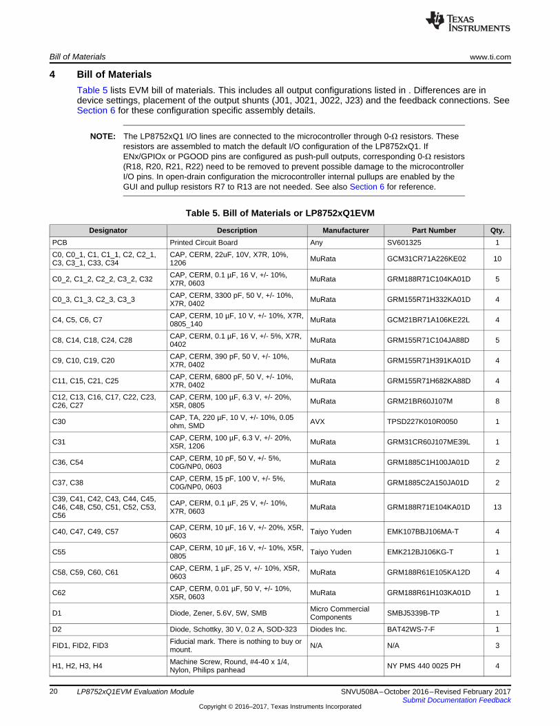
4 Bill of MaterialsTable 5 lists EVM bill of materials. This includes all output configurations listed in . Differences are indevice settings, placement of the output shunts (J01, J021, J022, J23) and the feedback connections. SeeSection 6 for these configuration specific assembly details.
NOTE: The LP8752xQ1 I/O lines are connected to the microcontroller through 0-Ω resistors. Theseresistors are assembled to match the default I/O configuration of the LP8752xQ1. IfENx/GPIOx or PGOOD pins are configured as push-pull outputs, corresponding 0-Ω resistors(R18, R20, R21, R22) need to be removed to prevent possible damage to the microcontrollerI/O pins. In open-drain configuration the microcontroller internal pullups are enabled by theGUI and pullup resistors R7 to R13 are not needed. See also Section 6 for reference.
Table 5. Bill of Materials or LP8752xQ1EVM
Designator Description Manufacturer Part Number Qty.PCB Printed Circuit Board Any SV601325 1C0, C0_1, C1, C1_1, C2, C2_1,C3, C3_1, C33, C34
CAP, CERM, 22uF, 10V, X7R, 10%,1206 MuRata GCM31CR71A226KE02 10
C0_2, C1_2, C2_2, C3_2, C32 CAP, CERM, 0.1 µF, 16 V, +/- 10%,X7R, 0603 MuRata GRM188R71C104KA01D 5
C0_3, C1_3, C2_3, C3_3 CAP, CERM, 3300 pF, 50 V, +/- 10%,X7R, 0402 MuRata GRM155R71H332KA01D 4
C4, C5, C6, C7 CAP, CERM, 10 µF, 10 V, +/- 10%, X7R,0805_140 MuRata GCM21BR71A106KE22L 4
C8, C14, C18, C24, C28 CAP, CERM, 0.1 µF, 16 V, +/- 5%, X7R,0402 MuRata GRM155R71C104JA88D 5
C9, C10, C19, C20 CAP, CERM, 390 pF, 50 V, +/- 10%,X7R, 0402 MuRata GRM155R71H391KA01D 4
C11, C15, C21, C25 CAP, CERM, 6800 pF, 50 V, +/- 10%,X7R, 0402 MuRata GRM155R71H682KA88D 4
C12, C13, C16, C17, C22, C23,C26, C27
CAP, CERM, 100 µF, 6.3 V, +/- 20%,X5R, 0805 MuRata GRM21BR60J107M 8
C30 CAP, TA, 220 µF, 10 V, +/- 10%, 0.05ohm, SMD AVX TPSD227K010R0050 1
C31 CAP, CERM, 100 µF, 6.3 V, +/- 20%,X5R, 1206 MuRata GRM31CR60J107ME39L 1
C36, C54 CAP, CERM, 10 pF, 50 V, +/- 5%,C0G/NP0, 0603 MuRata GRM1885C1H100JA01D 2
C37, C38 CAP, CERM, 15 pF, 100 V, +/- 5%,C0G/NP0, 0603 MuRata GRM1885C2A150JA01D 2
C39, C41, C42, C43, C44, C45,C46, C48, C50, C51, C52, C53,C56
CAP, CERM, 0.1 µF, 25 V, +/- 10%,X7R, 0603 MuRata GRM188R71E104KA01D 13
C40, C47, C49, C57 CAP, CERM, 10 µF, 16 V, +/- 20%, X5R,0603 Taiyo Yuden EMK107BBJ106MA-T 4
C55 CAP, CERM, 10 µF, 16 V, +/- 10%, X5R,0805 Taiyo Yuden EMK212BJ106KG-T 1
C58, C59, C60, C61 CAP, CERM, 1 µF, 25 V, +/- 10%, X5R,0603 MuRata GRM188R61E105KA12D 4
C62 CAP, CERM, 0.01 µF, 50 V, +/- 10%,X5R, 0603 MuRata GRM188R61H103KA01D 1
D1 Diode, Zener, 5.6V, 5W, SMB Micro CommercialComponents SMBJ5339B-TP 1
D2 Diode, Schottky, 30 V, 0.2 A, SOD-323 Diodes Inc. BAT42WS-7-F 1
FID1, FID2, FID3 Fiducial mark. There is nothing to buy ormount. N/A N/A 3
H1, H2, H3, H4 Machine Screw, Round, #4-40 x 1/4,Nylon, Philips panhead NY PMS 440 0025 PH 4
www.ti.com Bill of Materials
21SNVU508A–October 2016–Revised February 2017Submit Documentation Feedback
Copyright © 2016–2017, Texas Instruments Incorporated
LP8752xQ1EVM Evaluation Module
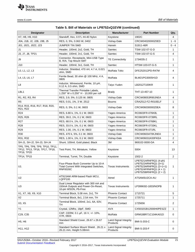
Table 5. Bill of Materials or LP8752xQ1EVM (continued)Designator Description Manufacturer Part Number Qty.
H7, H8, H9, H10 Standoff, Hex, 0.5"L #4-40 Nylon Keystone 1902C 4J0A, J1B, J2, J2B, J3B, J5 RES, 0, 5%, 0.063 W, 0402 Vishay-Dale CRCW04020000Z0ED 1 - 6J01, J021, J022, J23 JUMPER TIN SMD Harwin S1911-46R 0 - 4J1 Header, 100mil, 2x2, Gold, TH Samtec TSW-102-07-G-D 1J3, J7, J8, TP21 Header, 100mil, 2x1, Gold, TH Samtec TSW-102-07-G-S 4
J9 Connector, Receptacle, Mini-USB TypeB, R/A, Top Mount SMT TE Connectivity 1734035-2 1
J10 Header, 100mil, 3x1, Gold, TH Samtec HTSW-103-07-G-S 1
L0, L1, L2, L3 Inductor, Shielded, 470 nH, 4.7 A, 0.021ohm, SMD MuRata Toko DFE252012PD-R47M 4
L4, L5, L6, L7 Ferrite Bead, 30 ohm @ 100 MHz, 4 A,0805 MuRata BLM21PG300SH1D 4
L8 Inductor, Wirewound, Ferrite, 10 µH,0.12 A, 0.5 ohm, SMD Taiyo Yuden LB2012T100KR 1
LBL1 Thermal Transfer Printable Labels,1.250" W x 0.250" H - 10,000 per roll Brady THT-13-457-10 1
R1, R2, R3, R4 RES, 3.9, 5%, 0.125 W, 0805 Vishay-Dale CRCW08053R90JNEA 4R5 RES, 0.01, 1%, 3 W, 2512 Bourns CRA2512-FZ-R010ELF 1R14, R15, R16, R17, R18, R20,R21, R22 RES, 0, 5%, 0.1 W, 0603 Vishay-Dale CRCW06030000Z0EA 8
R24 RES, 6.80 k, 1%, 0.1 W, 0603 Yageo America RC0603FR-076K8L 1R25, R26 RES, 39.0, 1%, 0.1 W, 0603 Yageo America RC0603FR-0739RL 2R27 RES, 68.0 k, 1%, 0.1 W, 0603 Yageo America RC0603FR-0768KL 1R28 RES, 33.0 k, 1%, 0.1 W, 0603 Yageo America RC0603FR-0733KL 1R29 RES, 1.00, 1%, 0.1 W, 0603 Yageo America RC0603FR-071RL 1R30 RES, 470 k, 5%, 0.1 W, 0603 Vishay-Dale CRCW0603470KJNEA 1R31, R32 RES, 1.00 k, 1%, 0.1 W, 0603 Vishay-Dale CRCW06031K00FKEA 2SH-J1, SH-J2, SH-J3, SH-J4 Shunt, 100mil, Gold plated, Black 3M 969102-0000-DA 4TP5, TP6, TP8, TP9, TP10, TP11,TP12, TP13, TP16, TP17, TP18,TP19, TP20
Test Point, TH, Miniature, Yellow Keystone 5004 13
TP14, TP15 Terminal, Turret, TH, Double Keystone 1502-2 2
U1Four-Phase Buck Converter Up to 10-ATotal Current With Integrated Switches,RNF0026C
Texas Instruments
LP87521ARNFRQ1 (4-ph)LP87522ARNFRQ1 (3+1)LP87523ARNFRQ1 (2+1+1)LP87524FRNFRQ1 (4 × 1)LP87525BRNFRQ1 (2 + 2)
1
U2 AT91SAM ARM-based Flash MCU,LQFP100 Atmel ATSAM3U2CA-AU 1
U3Dual Linear Regulator with 300 mA and150mA Outputs and Power-On-Reset,10-pin WSON, Pb-Free
Texas Instruments LP3996SD-1833/NOPB 1
X1, X7, X8, X9, X10 Terminal Block, 5.08 mm, 2x1, TH Phoenix Contact 1715721 5X2 Terminal Block, 8x1, 2.54 mm, TH Phoenix Contact 1725711 1
X3, X5 Terminal Block, 100mil, 2x1, 6A, 63V,TH Phoenix Contact 1725656 2
Y1 Crystal, 12Mhz, 18pF, SMD AVX CX5032GB12000H0PESZZ 1
C29, C35 CAP, CERM, 0.1 µF, 16 V, +/- 10%,X7R, 0603 MuRata GRM188R71C104KA01D 0
H5, H6 Standard Shield Cover, 26.67 x 26.67mm
Laird-Signal IntegrityProducts BMI-S-203-C 0
H11, H12 Standard Surface Mount Shield , 26.21 x26.21 mm, Height 5.08mm
Laird-Signal IntegrityProducts BMI-S-203-F 0

Board Layout www.ti.com
22 SNVU508A–October 2016–Revised February 2017Submit Documentation Feedback
Copyright © 2016–2017, Texas Instruments Incorporated
LP8752xQ1EVM Evaluation Module
Table 5. Bill of Materials or LP8752xQ1EVM (continued)Designator Description Manufacturer Part Number Qty.
J1A, J2A, J3A, J4 RES, 0, 5%, 0.063 W, 0402 Vishay-Dale CRCW04020000Z0ED 0 - 4R6, R19 RES, 0, 5%, 0.1 W, 0603 Vishay-Dale CRCW06030000Z0EA 0R7, R8, R9, R10, R11, R12, R13 RES, 1.8 k, 5%, 0.1 W, 0603 Vishay-Dale CRCW06031K80JNEA 0R23 RES, 50, 1%, 0.1 W, 0603 Vishay-Dale CRCW060350R0FKEA 0TP1, TP2, TP3, TP4, TP7 Header, 100mil, 2x1, Gold, TH Samtec TSW-102-07-G-S 0X4, X6 Receptacle, 2.5mm, 3x2, Gold, SMT TE Connectivity 6651712-1 0
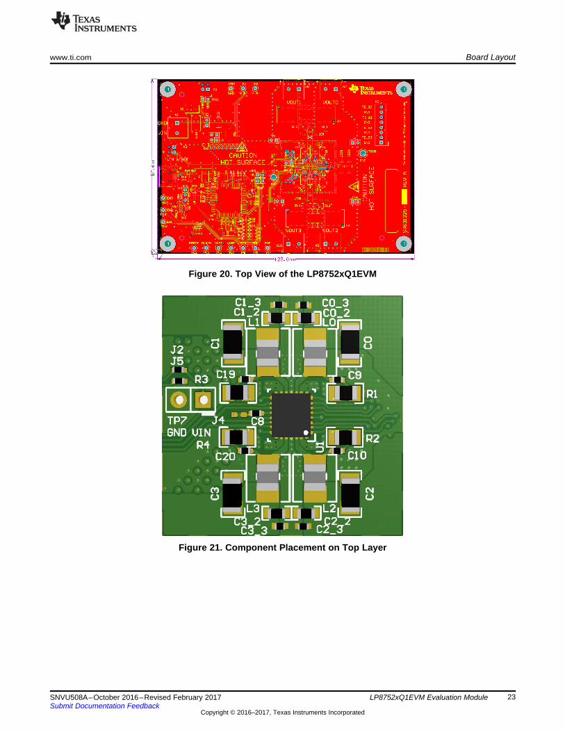
5 Board LayoutThis section describes the board layout of the LP8752xQ1EVM. See the LP8752 data sheet for specificPCB layout recommendations. The board is constructed on a 6-layer PCB using 60-µm copper on top andbottom layers to reduce resistance and improve heat transfer. Similar layout can be done as 4-layer boardbut 6 layers were chosen to improve grounding and reduce DC resistances.
Board stack-up is shown in Figure 19. shows the top view of the entire board and Figure 21 throughFigure 28 show the component placement, layout, and 3D view close to the LP8752xQ1 device.
Figure 19. Board Stack-Up
The design utilizes dual side placement of the components. This allows placement of the inductors next tothe LP8752xQ1 device for reducing SW node area for improved efficiency and reduced EMI. SW netshave also snubber components to reduce SW pin spiking and EMI. The input capacitors can be placedvery close to the LP8752xQ1 device, to bottom side, to keep parasitic inductances low, and there is alsospace for input filters for further EMI reduction. With these modifications, the EVMs can pass CISPR25radiated and conducted EMI test without (optional) EMI shields H5 and H6.
www.ti.com Board Layout
23SNVU508A–October 2016–Revised February 2017Submit Documentation Feedback
Copyright © 2016–2017, Texas Instruments Incorporated
LP8752xQ1EVM Evaluation Module
Figure 20. Top View of the LP8752xQ1EVM
Figure 21. Component Placement on Top Layer
Board Layout www.ti.com
24 SNVU508A–October 2016–Revised February 2017Submit Documentation Feedback
Copyright © 2016–2017, Texas Instruments Incorporated
LP8752xQ1EVM Evaluation Module
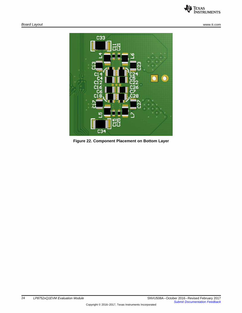
Figure 22. Component Placement on Bottom Layer

LP8752_EVM_mid3_layer
www.ti.com Board Layout
25SNVU508A–October 2016–Revised February 2017Submit Documentation Feedback
Copyright © 2016–2017, Texas Instruments Incorporated
LP8752xQ1EVM Evaluation Module
VIN nets are connected to bottom layer with multiple vias. This allows closer placement of the inductors, thusreducing SW node size and EMI. Also snubber circuits are placed next to SW nets for EMI reduction. Multiple GNDvias are used to provide solid ground around the LP8752xQ1 device.
Figure 23. Top Layer
Board Layout www.ti.com
26 SNVU508A–October 2016–Revised February 2017Submit Documentation Feedback
Copyright © 2016–2017, Texas Instruments Incorporated
LP8752xQ1EVM Evaluation Module
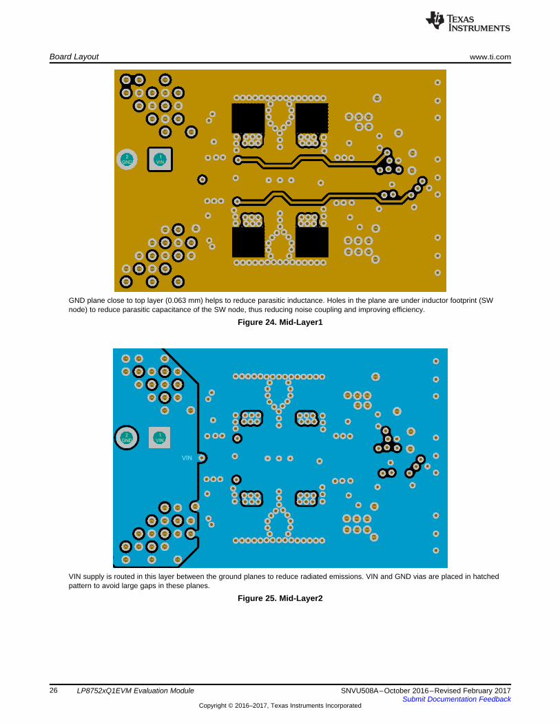
GND plane close to top layer (0.063 mm) helps to reduce parasitic inductance. Holes in the plane are under inductor footprint (SWnode) to reduce parasitic capacitance of the SW node, thus reducing noise coupling and improving efficiency.
Figure 24. Mid-Layer1
VIN supply is routed in this layer between the ground planes to reduce radiated emissions. VIN and GND vias are placed in hatchedpattern to avoid large gaps in these planes.
Figure 25. Mid-Layer2
www.ti.com Board Layout
27SNVU508A–October 2016–Revised February 2017Submit Documentation Feedback
Copyright © 2016–2017, Texas Instruments Incorporated
LP8752xQ1EVM Evaluation Module
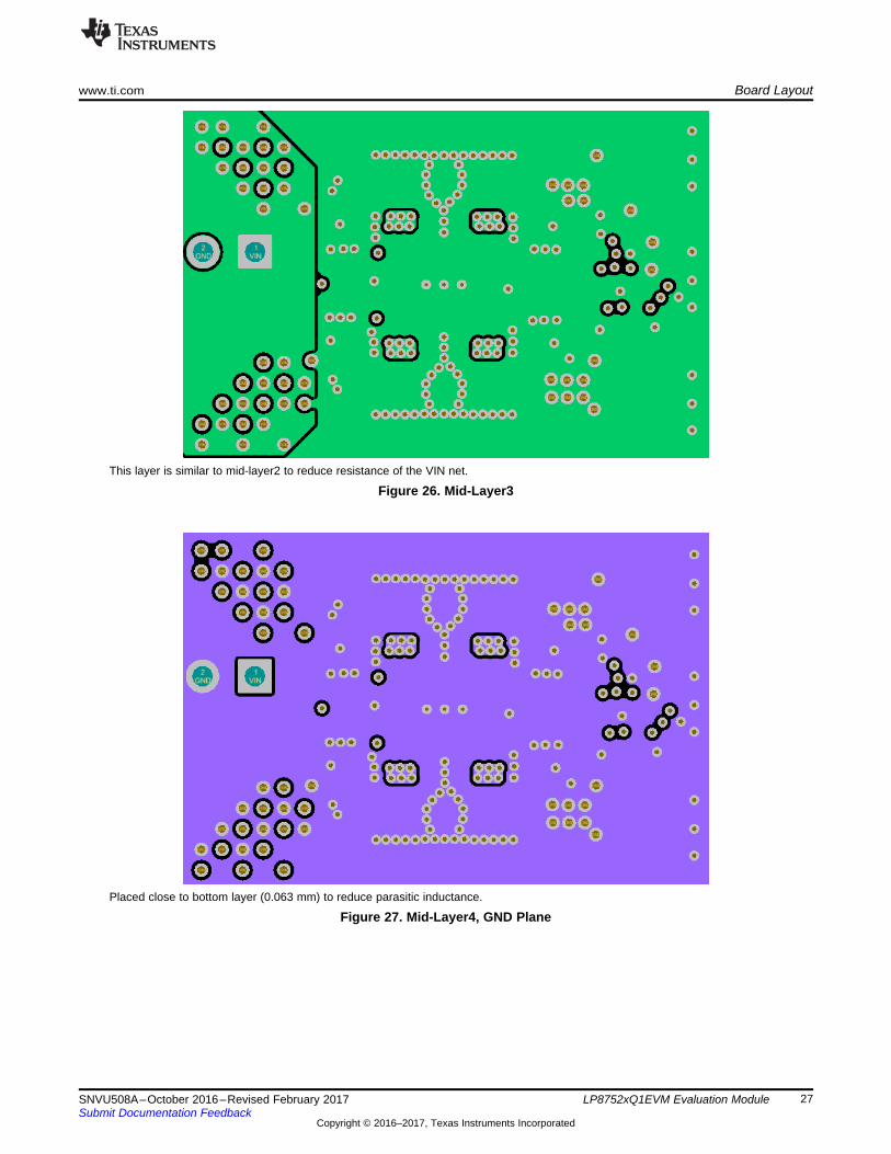
This layer is similar to mid-layer2 to reduce resistance of the VIN net.
Figure 26. Mid-Layer3
Placed close to bottom layer (0.063 mm) to reduce parasitic inductance.
Figure 27. Mid-Layer4, GND Plane
Board Layout www.ti.com
28 SNVU508A–October 2016–Revised February 2017Submit Documentation Feedback
Copyright © 2016–2017, Texas Instruments Incorporated
LP8752xQ1EVM Evaluation Module
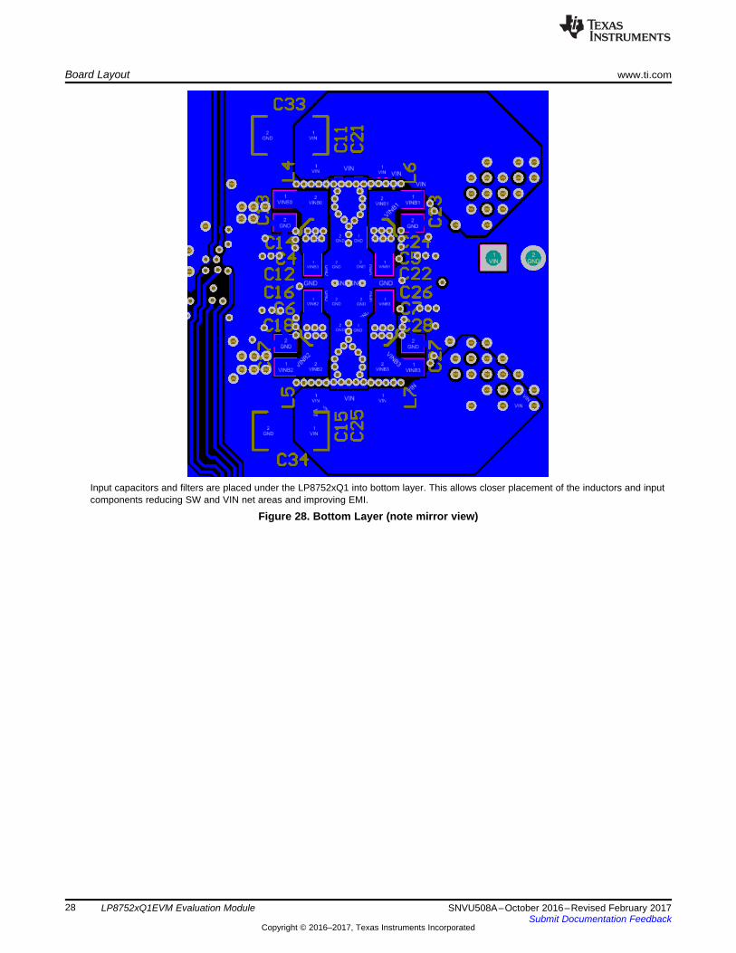
Input capacitors and filters are placed under the LP8752xQ1 into bottom layer. This allows closer placement of the inductors and inputcomponents reducing SW and VIN net areas and improving EMI.
Figure 28. Bottom Layer (note mirror view)

GND
GND
10µFC4
10µFC5
10µFC6
10µFC7
VINB0
VINB1
VINB2
VINB3
VINB0
VINB1
VINB2
VINB3
6800pF
C11100µFC12
VIN
GND GNDGND
6800pF
C21100µFC22
VIN
GND GNDGND
6800pF
C15100µFC16
VIN
GND GNDGND
6800pF
C25100µFC26
VIN
GND GNDGND
SW0
SW1
SW2
SW3
100µFC13
GND
100µFC23
GND
100µFC17
GND
100µFC27
GND
GND
GND
GND
GND
GND
GND
0J3B0J3A
DNP
GND
GND
1
2
TP1
DNP
1
2
TP2
DNP
1
2
TP3
DNP
1
2
TP4
DNP
GND
GND
GND
GND
0J0A
GND
GND
GND
GND
0J1B0J1A
DNP
FB0
FB1
FB2
FB3
FB1
FB0
FB2
FB3
0J2B0J2A
DNP
VOUT0
VOUT1
VOUT2
VOUT3
0.1µFC0_2
0.1µFC1_2
0.1µFC2_2
0.1µFC3_2
SW0
SW1
SW2
SW3
22µFC0
22µFC0_1
22µFC1
22µFC1_1
22µFC2
22µFC2_1
22µFC3
22µFC3_1
GND
SDASYS
SCLSYS
INT
NRST
PGOOD
CLKIN
EN1
EN2
EN3
3.9R1 390pF
C9
3.9R3 390pF
C19
3.9R2 390pF
C10
3.9R4 390pF
C20
3300pFC0_3
3300pFC1_3
3300pFC2_3
3300pFC3_3
Input filters for reducing EMISnubbers
VDDA
30 ohm
L4
BLM21PG300SH1D
30 ohm
L6
BLM21PG300SH1D
30 ohm
L5
BLM21PG300SH1D
30 ohm
L7
BLM21PG300SH1D
470nH
L0
470nH
L1
470nH
L2
470nH
L3
J01
S1911-46R
J021
S1911-46R
J23
S1911-46R
VOUT0
VOUT2
VOUT2
VOUT1
VOUT3
VOUT0
J022
S1911-46R
VOUT2VOUT0
Shunts for Connecting Phases Together
0.1µFC8
0.1µFC14
0.1µFC24
0.1µFC18
0.1µFC28
FB_B21
EN32
CLKIN3
AGND4
SCL5
SDA6
EN17
FB_B08
VIN_B09
SW_B010
PGND_B0111
SW_B112
VIN_B113
FB_B114
EN215
PGOOD16
AGND17
VANA18
INT19
NRST20
FB_B321
VIN_B322
SW_B323
PGND_B2324
SW_B225
VIN_B226
AGND27
U1
LP87521ARNFRQ1Copyright © 2016, Texas Instruments Incorporated
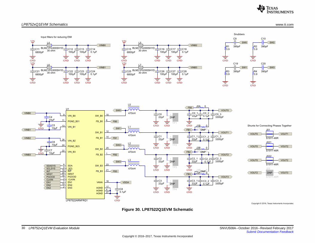
www.ti.com LP8752xQ1EVM Schematics
29SNVU508A–October 2016–Revised February 2017Submit Documentation Feedback
Copyright © 2016–2017, Texas Instruments Incorporated
LP8752xQ1EVM Evaluation Module
6 LP8752xQ1EVM Schematics
Figure 29. LP87521Q1EVM Schematic
GND
GND
10µFC4
10µFC5
10µFC6
10µFC7
VINB0
VINB1
VINB2
VINB3
VINB0
VINB1
VINB2
VINB3
6800pF
C11100µFC12
VIN
GND GNDGND
6800pF
C21100µFC22
VIN
GND GNDGND
6800pF
C15100µFC16
VIN
GND GNDGND
6800pF
C25100µFC26
VIN
GND GNDGND
SW0
SW1
SW2
SW3
100µFC13
GND
100µFC23
GND
100µFC17
GND
100µFC27
GND
GND
GND
GND
GND
GND
GND
0J3BDNP
0J3A
GND
GND
1
2
TP1
DNP
1
2
TP2
DNP
1
2
TP3
DNP
1
2
TP4
DNP
GND
GND
GND
GND
0J0A
GND
GND
GND
GND
0J1B0J1A
DNP
FB0
FB1
FB2
FB3
FB1
FB0
FB2
FB3
0J2B0J2A
DNP
VOUT0
VOUT1
VOUT2
VOUT3
0.1µFC0_2
0.1µFC1_2
0.1µFC2_2
0.1µFC3_2
SW0
SW1
SW2
SW3
22µFC0
22µFC0_1
22µFC1
22µFC1_1
22µFC2
22µFC2_1
22µFC3
22µFC3_1
GND
SDASYS
SCLSYS
INT
NRST
PGOOD
CLKIN
EN1
EN2
EN3
3.9R1 390pF
C9
3.9R3 390pF
C19
3.9R2 390pF
C10
3.9R4 390pF
C20
3300pFC0_3
3300pFC1_3
3300pFC2_3
3300pFC3_3
Input filters for reducing EMISnubbers
VDDA
30 ohm
L4
BLM21PG300SH1D
30 ohm
L6
BLM21PG300SH1D
30 ohm
L5
BLM21PG300SH1D
30 ohm
L7
BLM21PG300SH1D
470nH
L0
470nH
L1
470nH
L2
470nH
L3
J01
S1911-46R
J021
S1911-46R
J23
S1911-46R
DNP
VOUT0
VOUT2
VOUT2
VOUT1
VOUT3
VOUT0
J022
S1911-46R
VOUT2VOUT0
Shunts for Connecting Phases Together
0.1µFC8
0.1µFC14
0.1µFC24
0.1µFC18
0.1µFC28
FB_B21
EN32
CLKIN3
AGND4
SCL5
SDA6
EN17
FB_B08
VIN_B09
SW_B010
PGND_B0111
SW_B112
VIN_B113
FB_B114
EN215
PGOOD16
AGND17
VANA18
INT19
NRST20
FB_B321
VIN_B322
SW_B323
PGND_B2324
SW_B225
VIN_B226
AGND27
U1
LP87522ARNFRQ1Copyright © 2016, Texas Instruments Incorporated
LP8752xQ1EVM Schematics www.ti.com
30 SNVU508A–October 2016–Revised February 2017Submit Documentation Feedback
Copyright © 2016–2017, Texas Instruments Incorporated
LP8752xQ1EVM Evaluation Module
Figure 30. LP87522Q1EVM Schematic
GND
GND
10µFC4
10µFC5
10µFC6
10µFC7
VINB0
VINB1
VINB2
VINB3
VINB0
VINB1
VINB2
VINB3
6800pF
C11100µFC12
VIN
GND GNDGND
6800pF
C21100µFC22
VIN
GND GNDGND
6800pF
C15100µFC16
VIN
GND GNDGND
6800pF
C25100µFC26
VIN
GND GNDGND
SW0
SW1
SW2
SW3
100µFC13
GND
100µFC23
GND
100µFC17
GND
100µFC27
GND
GND
GND
GND
GND
GND
GND
0J3BDNP
0J3A
GND
GND
1
2
TP1
DNP
1
2
TP2
DNP
1
2
TP3
DNP
1
2
TP4
DNP
GND
GND
GND
GND
0J0A
GND
GND
GND
GND
0J1B0J1A
DNP
FB0
FB1
FB2
FB3
FB1
FB0
FB2
FB3
0J2BDNP
0J2A
VOUT0
VOUT1
VOUT2
VOUT3
0.1µFC0_2
0.1µFC1_2
0.1µFC2_2
0.1µFC3_2
SW0
SW1
SW2
SW3
22µFC0
22µFC0_1
22µFC1
22µFC1_1
22µFC2
22µFC2_1
22µFC3
22µFC3_1
GND
SDASYS
SCLSYS
INT
NRST
PGOOD
CLKIN
EN1
EN2
EN3
3.9R1 390pF
C9
3.9R3 390pF
C19
3.9R2 390pF
C10
3.9R4 390pF
C20
3300pFC0_3
3300pFC1_3
3300pFC2_3
3300pFC3_3
Input filters for reducing EMISnubbers
VDDA
30 ohm
L4
BLM21PG300SH1D
30 ohm
L6
BLM21PG300SH1D
30 ohm
L5
BLM21PG300SH1D
30 ohm
L7
BLM21PG300SH1D
470nH
L0
470nH
L1
470nH
L2
470nH
L3
J01
S1911-46R
J021
S1911-46R
DNP
J23
S1911-46R
DNP
VOUT0
VOUT2
VOUT2
VOUT1
VOUT3
VOUT0
J022
S1911-46R
DNP VOUT2VOUT0
Shunts for Connecting Phases Together
0.1µFC8
0.1µFC14
0.1µFC24
0.1µFC18
0.1µFC28
FB_B21
EN32
CLKIN3
AGND4
SCL5
SDA6
EN17
FB_B08
VIN_B09
SW_B010
PGND_B0111
SW_B112
VIN_B113
FB_B114
EN215
PGOOD16
AGND17
VANA18
INT19
NRST20
FB_B321
VIN_B322
SW_B323
PGND_B2324
SW_B225
VIN_B226
AGND27
U1
LP87523ARNFRQ1Copyright © 2016, Texas Instruments Incorporated
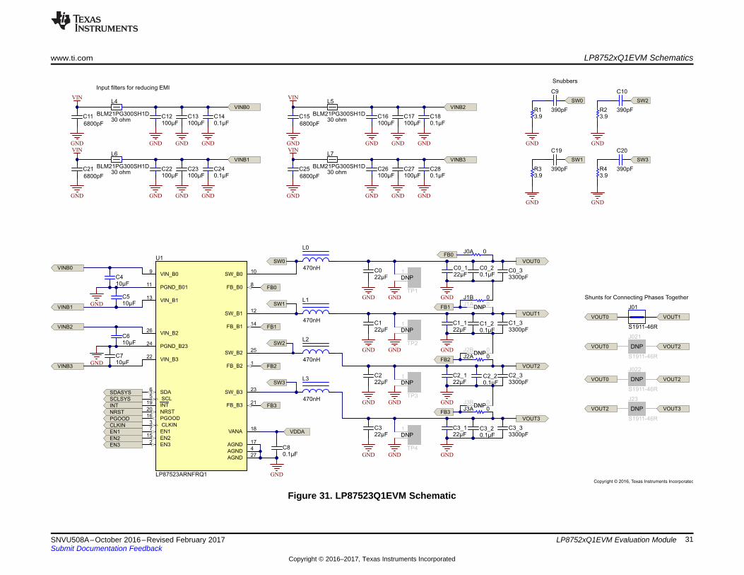
www.ti.com LP8752xQ1EVM Schematics
31SNVU508A–October 2016–Revised February 2017Submit Documentation Feedback
Copyright © 2016–2017, Texas Instruments Incorporated
LP8752xQ1EVM Evaluation Module
Figure 31. LP87523Q1EVM Schematic
GND
GND
10µFC4
10µFC5
10µFC6
10µFC7
VINB0
VINB1
VINB2
VINB3
VINB0
VINB1
VINB2
VINB3
6800pF
C11100µFC12
VIN
GND GNDGND
6800pF
C21100µFC22
VIN
GND GNDGND
6800pF
C15100µFC16
VIN
GND GNDGND
6800pF
C25100µFC26
VIN
GND GNDGND
SW0
SW1
SW2
SW3
100µFC13
GND
100µFC23
GND
100µFC17
GND
100µFC27
GND
GND
GND
GND
GND
GND
GND
0J3BDNP
0J3A
GND
GND
1
2
TP1
DNP
1
2
TP2
DNP
1
2
TP3
DNP
1
2
TP4
DNP
GND
GND
GND
GND
0J0A
GND
GND
GND
GND
0J1BDNP
0J1A
FB0
FB1
FB2
FB3
FB1
FB0
FB2
FB3
0J2BDNP
0J2A
VOUT0
VOUT1
VOUT2
VOUT3
0.1µFC0_2
0.1µFC1_2
0.1µFC2_2
0.1µFC3_2
SW0
SW1
SW2
SW3
22µFC0
22µFC0_1
22µFC1
22µFC1_1
22µFC2
22µFC2_1
22µFC3
22µFC3_1
GND
SDASYS
SCLSYS
INT
NRST
PGOOD
CLKIN
EN1
EN2
EN3
3.9R1 390pF
C9
3.9R3 390pF
C19
3.9R2 390pF
C10
3.9R4 390pF
C20
3300pFC0_3
3300pFC1_3
3300pFC2_3
3300pFC3_3
Input filters for reducing EMISnubbers
VDDA
30 ohm
L4
BLM21PG300SH1D
30 ohm
L6
BLM21PG300SH1D
30 ohm
L5
BLM21PG300SH1D
30 ohm
L7
BLM21PG300SH1D
470nH
L0
470nH
L1
470nH
L2
470nH
L3
J01
S1911-46R
DNP
J021
S1911-46R
DNP
J23
S1911-46R
DNP
VOUT0
VOUT2
VOUT2
VOUT1
VOUT3
VOUT0
J022
S1911-46R
DNP VOUT2VOUT0
Shunts for Connecting Phases Together
0.1µFC8
0.1µFC14
0.1µFC24
0.1µFC18
0.1µFC28
FB_B21
EN32
CLKIN3
AGND4
SCL5
SDA6
EN17
FB_B08
VIN_B09
SW_B010
PGND_B0111
SW_B112
VIN_B113
FB_B114
EN215
PGOOD16
AGND17
VANA18
INT19
NRST20
FB_B321
VIN_B322
SW_B323
PGND_B2324
SW_B225
VIN_B226
AGND27
U1
LP87524FRNFRQ1Copyright © 2016, Texas Instruments Incorporated
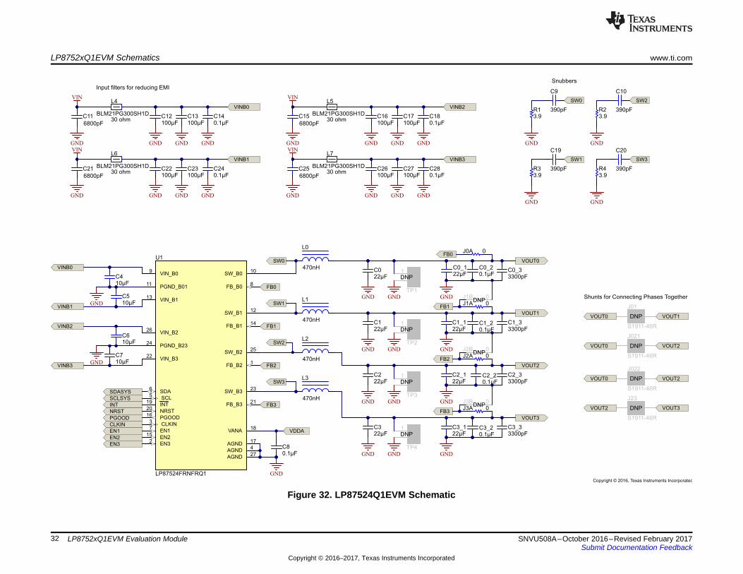
LP8752xQ1EVM Schematics www.ti.com
32 SNVU508A–October 2016–Revised February 2017Submit Documentation Feedback
Copyright © 2016–2017, Texas Instruments Incorporated
LP8752xQ1EVM Evaluation Module
Figure 32. LP87524Q1EVM Schematic
GND
GND
10µFC4
10µFC5
10µFC6
10µFC7
VINB0
VINB1
VINB2
VINB3
VINB0
VINB1
VINB2
VINB3
6800pF
C11100µFC12
VIN
GND GNDGND
6800pF
C21100µFC22
VIN
GND GNDGND
6800pF
C15100µFC16
VIN
GND GNDGND
6800pF
C25100µFC26
VIN
GND GNDGND
SW0
SW1
SW2
SW3
100µFC13
GND
100µFC23
GND
100µFC17
GND
100µFC27
GND
GND
GND
GND
GND
GND
GND
0J3B0J3A
DNP
GND
GND
1
2
TP1
DNP
1
2
TP2
DNP
1
2
TP3
DNP
1
2
TP4
DNP
GND
GND
GND
GND
0J0A
GND
GND
GND
GND
0J1B0J1A
DNP
FB0
FB1
FB2
FB3
FB1
FB0
FB2
FB3
0J2BDNP
0J2A
VOUT0
VOUT1
VOUT2
VOUT3
0.1µFC0_2
0.1µFC1_2
0.1µFC2_2
0.1µFC3_2
SW0
SW1
SW2
SW3
22µFC0
22µFC0_1
22µFC1
22µFC1_1
22µFC2
22µFC2_1
22µFC3
22µFC3_1
GND
SDASYS
SCLSYS
INT
NRST
PGOOD
CLKIN
EN1
EN2
EN3
3.9R1 390pF
C9
3.9R3 390pF
C19
3.9R2 390pF
C10
3.9R4 390pF
C20
3300pFC0_3
3300pFC1_3
3300pFC2_3
3300pFC3_3
Input filters for reducing EMISnubbers
VDDA
30 ohm
L4
BLM21PG300SH1D
30 ohm
L6
BLM21PG300SH1D
30 ohm
L5
BLM21PG300SH1D
30 ohm
L7
BLM21PG300SH1D
470nH
L0
470nH
L1
470nH
L2
470nH
L3
J01
S1911-46R
J021
S1911-46R
DNP
J23
S1911-46R
VOUT0
VOUT2
VOUT2
VOUT1
VOUT3
VOUT0
J022
S1911-46R
DNP VOUT2VOUT0
Shunts for Connecting Phases Together
0.1µFC8
0.1µFC14
0.1µFC24
0.1µFC18
0.1µFC28
FB_B21
EN32
CLKIN3
AGND4
SCL5
SDA6
EN17
FB_B08
VIN_B09
SW_B010
PGND_B0111
SW_B112
VIN_B113
FB_B114
EN215
PGOOD16
AGND17
VANA18
INT19
NRST20
FB_B321
VIN_B322
SW_B323
PGND_B2324
SW_B225
VIN_B226
AGND27
U1
LP87525BRNFRQ1Copyright © 2016, Texas Instruments Incorporated
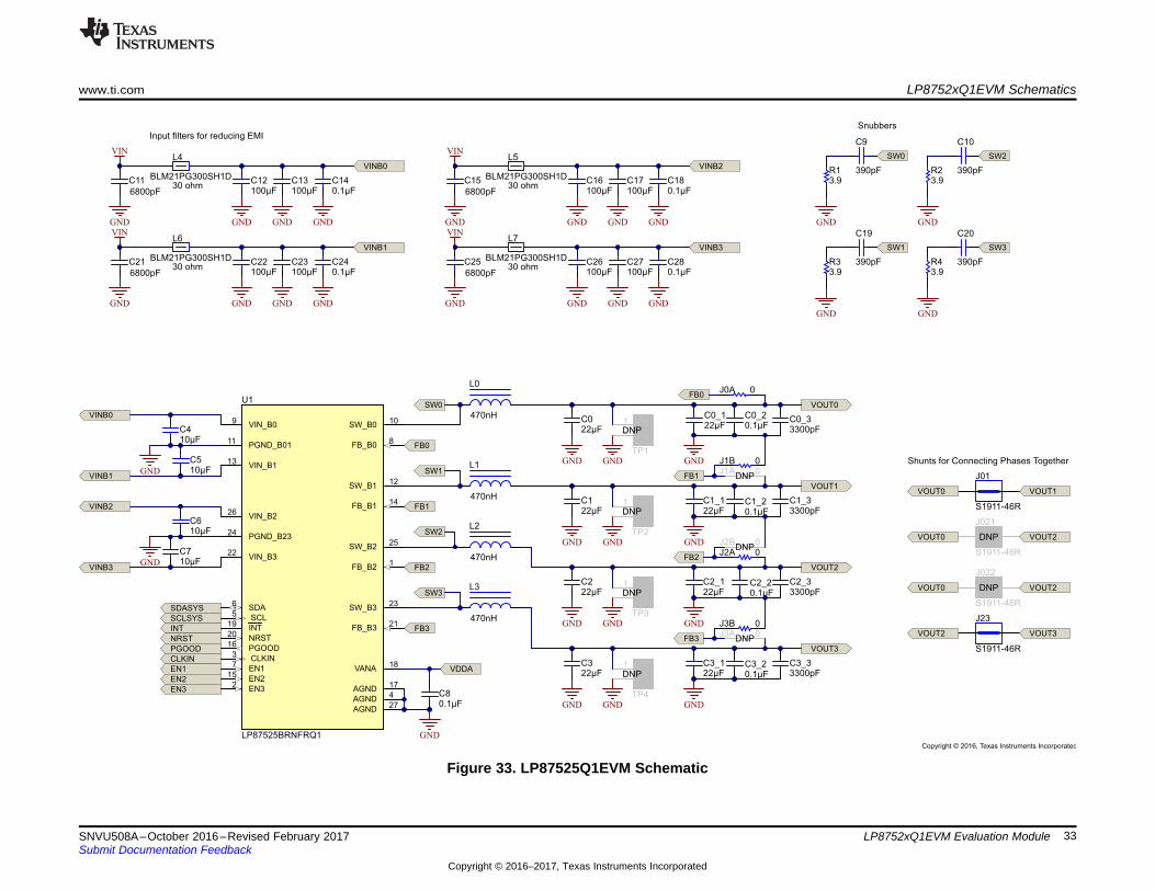
www.ti.com LP8752xQ1EVM Schematics
33SNVU508A–October 2016–Revised February 2017Submit Documentation Feedback
Copyright © 2016–2017, Texas Instruments Incorporated
LP8752xQ1EVM Evaluation Module
Figure 33. LP87525Q1EVM Schematic
TP20
GND
1
2
X3
1725656
GND
1
2
TP21
1
2
X5
1725656
Vin_sense+
Vin_sense-
SDASYS
SCLSYS
INT
NRST
PGOOD
CLKIN
EN1
EN2
EN3
VIOSYS
TP8
TP9
TP10
TP11
TP12
TP13
TP16
TP19
TP18
GND
220µFC30
GND
TP5 TP6
GND
Vin11
2
X1
1715721
0
J50
J4DNP
NT1
Net-Tie
1
2 J3
GND
D1
100µFC31
1 2
3 4
J1
0
J2
1
2
TP7
DNP
0.01
R5VIN
Vin_sense+
Vin_sense-
GND GND GND
GND
0.1µFC32
0.1µFC29DNP
0.1µFC35DNP
GND
GND
22µFC33
22µFC34
High dI/dt Power Connectors
Output Power Connectors
1
2
X7
1715721
1
2
X8
1715721
1
2
X9
1715721
1
2
X10
1715721
VOUT0
VOUT1
VOUT3
VOUT2
VOUT2
VOUT1
VOUT0
VOUT3
GND GND
GNDGND
GNDGND
12
34
56
X4
6651712-1
DNP
12
34
56
X6
6651712-1
DNP
VOUT0
VOUT1
VOUT3
VOUT2
GNDGND
Feedback Connector
5
4
1
2
3
6
7
8
X2GND
FB0
FB1
FB2
FB3
1.8kR7
DNP 1.8kR8
DNP 1.8kR9
DNP
0R140R150R160R170R180R19
DNP
SDASCL
HSI2C_SYS
0
R6DNP
0R210R22
0R20
1.8kR10
DNP
1
2
J7
1
2
J8
50
R23DNP
VCC1V8
INTB2B
NRSTB2B
EN1B2B
EN2B2B
EN3B2B
PGOODB2B
CLKINB2B
SDASYS
SCLSYS
INT
NRST
PGOOD
CLKIN
EN1
EN2
EN3
EN1B2B
EN2B2B
EN1
EN2
CLKIN
GND
1.8kR11
DNP 1.8kR12
DNP 1.8kR13
DNP
I/O signals
Current Measurement
TP17
GND
TP14TP15
VDDA
VIOSYS
VIN
Copyright © 2016, Texas Instruments Incorporated
LP8752xQ1EVM Schematics www.ti.com
34 SNVU508A–October 2016–Revised February 2017Submit Documentation Feedback
Copyright © 2016–2017, Texas Instruments Incorporated
LP8752xQ1EVM Evaluation Module
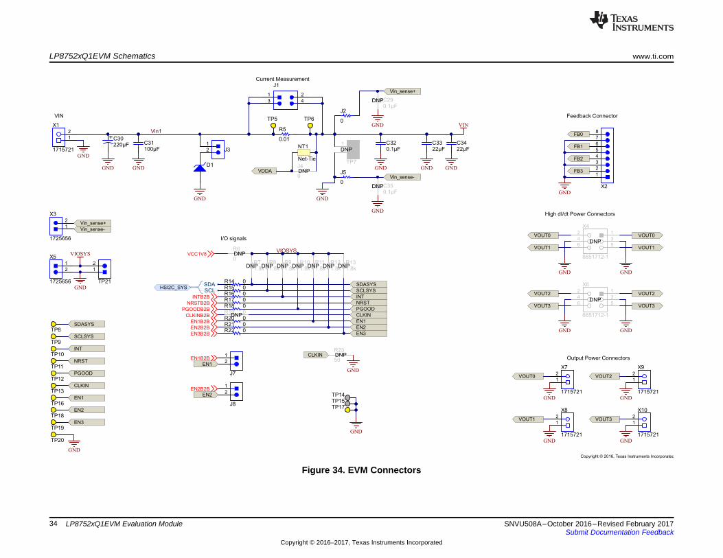
Figure 34. EVM Connectors

VUSB
15pFC37
15pFC38
GND GND
XO
UT
XIN
DHSDM
0.1µFC44
0.1µFC43
0.1µFC45
0.1µFC42
0.1µFC41
GND
10µFC40
JTAGSEL48
TCK/SWCLK56
TDI51
TDO/TRACESWO54
TMS/SWDIO55
U2C
ATSAM3U2CA-AUGNDBU
46ADVREF
2
AD12BVREF4
GNDANA3
GND35
GND61
GND89
GNDPLL72
VDDOUT52
VDDIN53
VDDIO60
VDDIO88
VDDCORE9
VDDCORE34
VDDANA1
VDDBU45
VDDPLL73
VDDCORE59
VDDCORE83
VDDCORE87
VDDIO36
VDDIO22
U2D
ATSAM3U2CA-AU
XOUT
XIN
GND
VUTMI
6.80kR24
GND
10pFC36
39.0R26
39.0R25
GND
DHSDP
DHSDM
VBG
GND
0.1µFC51
GND
10µFC49
HSI2C_SYS SCLSDA
PU_ENHS_I2C
1.00kR31
1.00kR32
1µFC61
GND
GND
10µFC57
1.00R29
0.1µFC56
+3.3V VUTMI
GND
10pFC54
10µFC55
DHSDP
VBUS_USB0.1µFC50
0.1µFC52
0.1µFC53
0.1µFC48
GND
10µFC47
TP22
PA0/PGMNCMD26
PA1/PGMRDY27
PA10/PGMD239
PA11/PGMD340
PA12/PGMD441
PA13/PGMD510
PA14/PGMD611
PA15/PGMD712
PA16/PGMD813
PA17/PGMD914
PA18/PGMD1017
PA19/PGMD1118
PA2/PGMNOE28
PA20/PGMD1219
PA21/PGMD1320
PA22/PGMD145
PA23/PGMD1521
PA2423
PA2524
PA2625
PA2796
PA2884
PA2985
PA3/PGMNVALID29
PA306
PA3186
PA4/PGMM030
PA5/PGMM131
PA6/PGMM232
PA7/PGMM333
PA8/PGMD037
PA9/PGMD138
PB090
PB191
PB1070
PB1193
PB1294
PB1395
PB1469
PB1516
PB1615
PB1768
PB1867
PB1966
PB292
PB2065
PB2164
PB2263
PB2362
PB2458
PB37
PB48
PB597
PB698
PB799
PB8100
PB971
U2A
ATSAM3U2CA-AU
DHSDP76
DHSDM77
FWUP42
NRST57
XOUT3249
TST44
ERASE43
NRSTB47
XIN3250
XOUT74
XIN75
VBG78
DFSDM80
DFSDP81
VDDUTMI79
GNDUTMI82
U2B
ATSAM3U2CA-AU
LDO1: 1.8 V (150 mA), VDDIO for SAM3ULDO2: 3.3 V (300 mA), 3.3V generic supply
IN1
NC7
EN12
OUT29
EN23
DAP11
POR8
OUT110
SET5
GND6
CBYP4
U3
LP3996SD-1833/NOPB
+3.3V
GND
GNDGND
VUSB
GND GND
0.01µFC62
1µFC60
1µFC59
1µFC58
470k
R30
GND
L8
LB2012T100KR
1
2
3
J10
HTSW-103-07-G-S
VIO +3.3V
+3.3V
VIO
VDDOUT
VDDOUT
CLKINB2B
1V8out
D2BAT42WS-7-F
68.0k
R27
VIO
0.1µFC39
+3.3V
Diode for clampingvoltage to IO level(1.8V/3.3V).
DFSDMDFSDP12MHz
12Y1
GND
0.1µFC46
GND
GND
89
VBUS1
GND5
67
D-2
D+3
ID4
J9
1734035-2
GND
33.0kR28
GND
VBUS_USB
SCLHSI2C_SYS
HSI2C_SYS SDA
HSI2C_SYS PU_EN
VCC1V8
INTB2B
NRSTB2B
EN1B2B
EN2B2B
EN3B2B
PGOODB2B
I2C Pull-up
I/O supply
Copyright © 2016, Texas Instruments Incorporated
www.ti.com LP8752xQ1EVM Schematics
35SNVU508A–October 2016–Revised February 2017Submit Documentation Feedback
Copyright © 2016–2017, Texas Instruments Incorporated
LP8752xQ1EVM Evaluation Module
Figure 35. EVM I2C Interface
Revision History www.ti.com
36 SNVU508A–October 2016–Revised February 2017Submit Documentation Feedback
Copyright © 2016–2017, Texas Instruments Incorporated
Revision History
Revision HistoryNOTE: Page numbers for previous revisions may differ from page numbers in the current version.
Changes from Original (October 2016) to A Revision .................................................................................................... Page
• Changed number of outputs for LP87525Q1 from "5" to "2"; added caution graphic ............................................ 3

STANDARD TERMS FOR EVALUATION MODULES1. Delivery: TI delivers TI evaluation boards, kits, or modules, including any accompanying demonstration software, components, and/or
documentation which may be provided together or separately (collectively, an “EVM” or “EVMs”) to the User (“User”) in accordancewith the terms set forth herein. User's acceptance of the EVM is expressly subject to the following terms.1.1 EVMs are intended solely for product or software developers for use in a research and development setting to facilitate feasibility
evaluation, experimentation, or scientific analysis of TI semiconductors products. EVMs have no direct function and are notfinished products. EVMs shall not be directly or indirectly assembled as a part or subassembly in any finished product. Forclarification, any software or software tools provided with the EVM (“Software”) shall not be subject to the terms and conditionsset forth herein but rather shall be subject to the applicable terms that accompany such Software
1.2 EVMs are not intended for consumer or household use. EVMs may not be sold, sublicensed, leased, rented, loaned, assigned,or otherwise distributed for commercial purposes by Users, in whole or in part, or used in any finished product or productionsystem.
2 Limited Warranty and Related Remedies/Disclaimers:2.1 These terms do not apply to Software. The warranty, if any, for Software is covered in the applicable Software License
Agreement.2.2 TI warrants that the TI EVM will conform to TI's published specifications for ninety (90) days after the date TI delivers such EVM
to User. Notwithstanding the foregoing, TI shall not be liable for a nonconforming EVM if (a) the nonconformity was caused byneglect, misuse or mistreatment by an entity other than TI, including improper installation or testing, or for any EVMs that havebeen altered or modified in any way by an entity other than TI, (b) the nonconformity resulted from User's design, specificationsor instructions for such EVMs or improper system design, or (c) User has not paid on time. Testing and other quality controltechniques are used to the extent TI deems necessary. TI does not test all parameters of each EVM.User's claims against TI under this Section 2 are void if User fails to notify TI of any apparent defects in the EVMs within ten (10)business days after delivery, or of any hidden defects with ten (10) business days after the defect has been detected.
2.3 TI's sole liability shall be at its option to repair or replace EVMs that fail to conform to the warranty set forth above, or creditUser's account for such EVM. TI's liability under this warranty shall be limited to EVMs that are returned during the warrantyperiod to the address designated by TI and that are determined by TI not to conform to such warranty. If TI elects to repair orreplace such EVM, TI shall have a reasonable time to repair such EVM or provide replacements. Repaired EVMs shall bewarranted for the remainder of the original warranty period. Replaced EVMs shall be warranted for a new full ninety (90) daywarranty period.
3 Regulatory Notices:3.1 United States
3.1.1 Notice applicable to EVMs not FCC-Approved:FCC NOTICE: This kit is designed to allow product developers to evaluate electronic components, circuitry, or softwareassociated with the kit to determine whether to incorporate such items in a finished product and software developers to writesoftware applications for use with the end product. This kit is not a finished product and when assembled may not be resold orotherwise marketed unless all required FCC equipment authorizations are first obtained. Operation is subject to the conditionthat this product not cause harmful interference to licensed radio stations and that this product accept harmful interference.Unless the assembled kit is designed to operate under part 15, part 18 or part 95 of this chapter, the operator of the kit mustoperate under the authority of an FCC license holder or must secure an experimental authorization under part 5 of this chapter.3.1.2 For EVMs annotated as FCC – FEDERAL COMMUNICATIONS COMMISSION Part 15 Compliant:
CAUTIONThis device complies with part 15 of the FCC Rules. Operation is subject to the following two conditions: (1) This device may notcause harmful interference, and (2) this device must accept any interference received, including interference that may causeundesired operation.Changes or modifications not expressly approved by the party responsible for compliance could void the user's authority tooperate the equipment.
FCC Interference Statement for Class A EVM devicesNOTE: This equipment has been tested and found to comply with the limits for a Class A digital device, pursuant to part 15 ofthe FCC Rules. These limits are designed to provide reasonable protection against harmful interference when the equipment isoperated in a commercial environment. This equipment generates, uses, and can radiate radio frequency energy and, if notinstalled and used in accordance with the instruction manual, may cause harmful interference to radio communications.Operation of this equipment in a residential area is likely to cause harmful interference in which case the user will be required tocorrect the interference at his own expense.
FCC Interference Statement for Class B EVM devicesNOTE: This equipment has been tested and found to comply with the limits for a Class B digital device, pursuant to part 15 ofthe FCC Rules. These limits are designed to provide reasonable protection against harmful interference in a residentialinstallation. This equipment generates, uses and can radiate radio frequency energy and, if not installed and used in accordancewith the instructions, may cause harmful interference to radio communications. However, there is no guarantee that interferencewill not occur in a particular installation. If this equipment does cause harmful interference to radio or television reception, whichcan be determined by turning the equipment off and on, the user is encouraged to try to correct the interference by one or moreof the following measures:
• Reorient or relocate the receiving antenna.• Increase the separation between the equipment and receiver.• Connect the equipment into an outlet on a circuit different from that to which the receiver is connected.• Consult the dealer or an experienced radio/TV technician for help.
3.2 Canada3.2.1 For EVMs issued with an Industry Canada Certificate of Conformance to RSS-210
Concerning EVMs Including Radio Transmitters:This device complies with Industry Canada license-exempt RSS standard(s). Operation is subject to the following two conditions:(1) this device may not cause interference, and (2) this device must accept any interference, including interference that maycause undesired operation of the device.
Concernant les EVMs avec appareils radio:Le présent appareil est conforme aux CNR d'Industrie Canada applicables aux appareils radio exempts de licence. L'exploitationest autorisée aux deux conditions suivantes: (1) l'appareil ne doit pas produire de brouillage, et (2) l'utilisateur de l'appareil doitaccepter tout brouillage radioélectrique subi, même si le brouillage est susceptible d'en compromettre le fonctionnement.
Concerning EVMs Including Detachable Antennas:Under Industry Canada regulations, this radio transmitter may only operate using an antenna of a type and maximum (or lesser)gain approved for the transmitter by Industry Canada. To reduce potential radio interference to other users, the antenna typeand its gain should be so chosen that the equivalent isotropically radiated power (e.i.r.p.) is not more than that necessary forsuccessful communication. This radio transmitter has been approved by Industry Canada to operate with the antenna typeslisted in the user guide with the maximum permissible gain and required antenna impedance for each antenna type indicated.Antenna types not included in this list, having a gain greater than the maximum gain indicated for that type, are strictly prohibitedfor use with this device.
Concernant les EVMs avec antennes détachablesConformément à la réglementation d'Industrie Canada, le présent émetteur radio peut fonctionner avec une antenne d'un type etd'un gain maximal (ou inférieur) approuvé pour l'émetteur par Industrie Canada. Dans le but de réduire les risques de brouillageradioélectrique à l'intention des autres utilisateurs, il faut choisir le type d'antenne et son gain de sorte que la puissance isotroperayonnée équivalente (p.i.r.e.) ne dépasse pas l'intensité nécessaire à l'établissement d'une communication satisfaisante. Leprésent émetteur radio a été approuvé par Industrie Canada pour fonctionner avec les types d'antenne énumérés dans lemanuel d’usage et ayant un gain admissible maximal et l'impédance requise pour chaque type d'antenne. Les types d'antennenon inclus dans cette liste, ou dont le gain est supérieur au gain maximal indiqué, sont strictement interdits pour l'exploitation del'émetteur
3.3 Japan3.3.1 Notice for EVMs delivered in Japan: Please see http://www.tij.co.jp/lsds/ti_ja/general/eStore/notice_01.page 日本国内に
輸入される評価用キット、ボードについては、次のところをご覧ください。http://www.tij.co.jp/lsds/ti_ja/general/eStore/notice_01.page
3.3.2 Notice for Users of EVMs Considered “Radio Frequency Products” in Japan: EVMs entering Japan may not be certifiedby TI as conforming to Technical Regulations of Radio Law of Japan.
If User uses EVMs in Japan, not certified to Technical Regulations of Radio Law of Japan, User is required to follow theinstructions set forth by Radio Law of Japan, which includes, but is not limited to, the instructions below with respect to EVMs(which for the avoidance of doubt are stated strictly for convenience and should be verified by User):1. Use EVMs in a shielded room or any other test facility as defined in the notification #173 issued by Ministry of Internal
Affairs and Communications on March 28, 2006, based on Sub-section 1.1 of Article 6 of the Ministry’s Rule forEnforcement of Radio Law of Japan,
2. Use EVMs only after User obtains the license of Test Radio Station as provided in Radio Law of Japan with respect toEVMs, or
3. Use of EVMs only after User obtains the Technical Regulations Conformity Certification as provided in Radio Law of Japanwith respect to EVMs. Also, do not transfer EVMs, unless User gives the same notice above to the transferee. Please notethat if User does not follow the instructions above, User will be subject to penalties of Radio Law of Japan.

【無線電波を送信する製品の開発キットをお使いになる際の注意事項】 開発キットの中には技術基準適合証明を受けていないものがあります。 技術適合証明を受けていないもののご使用に際しては、電波法遵守のため、以下のいずれかの措置を取っていただく必要がありますのでご注意ください。1. 電波法施行規則第6条第1項第1号に基づく平成18年3月28日総務省告示第173号で定められた電波暗室等の試験設備でご使用
いただく。2. 実験局の免許を取得後ご使用いただく。3. 技術基準適合証明を取得後ご使用いただく。
なお、本製品は、上記の「ご使用にあたっての注意」を譲渡先、移転先に通知しない限り、譲渡、移転できないものとします。上記を遵守頂けない場合は、電波法の罰則が適用される可能性があることをご留意ください。 日本テキサス・イ
ンスツルメンツ株式会社東京都新宿区西新宿6丁目24番1号西新宿三井ビル
3.3.3 Notice for EVMs for Power Line Communication: Please see http://www.tij.co.jp/lsds/ti_ja/general/eStore/notice_02.page電力線搬送波通信についての開発キットをお使いになる際の注意事項については、次のところをご覧ください。http://www.tij.co.jp/lsds/ti_ja/general/eStore/notice_02.page
3.4 European Union3.4.1 For EVMs subject to EU Directive 2014/30/EU (Electromagnetic Compatibility Directive):
This is a class A product intended for use in environments other than domestic environments that are connected to alow-voltage power-supply network that supplies buildings used for domestic purposes. In a domestic environment thisproduct may cause radio interference in which case the user may be required to take adequate measures.
4 EVM Use Restrictions and Warnings:4.1 EVMS ARE NOT FOR USE IN FUNCTIONAL SAFETY AND/OR SAFETY CRITICAL EVALUATIONS, INCLUDING BUT NOT
LIMITED TO EVALUATIONS OF LIFE SUPPORT APPLICATIONS.4.2 User must read and apply the user guide and other available documentation provided by TI regarding the EVM prior to handling
or using the EVM, including without limitation any warning or restriction notices. The notices contain important safety informationrelated to, for example, temperatures and voltages.
4.3 Safety-Related Warnings and Restrictions:4.3.1 User shall operate the EVM within TI’s recommended specifications and environmental considerations stated in the user
guide, other available documentation provided by TI, and any other applicable requirements and employ reasonable andcustomary safeguards. Exceeding the specified performance ratings and specifications (including but not limited to inputand output voltage, current, power, and environmental ranges) for the EVM may cause personal injury or death, orproperty damage. If there are questions concerning performance ratings and specifications, User should contact a TIfield representative prior to connecting interface electronics including input power and intended loads. Any loads appliedoutside of the specified output range may also result in unintended and/or inaccurate operation and/or possiblepermanent damage to the EVM and/or interface electronics. Please consult the EVM user guide prior to connecting anyload to the EVM output. If there is uncertainty as to the load specification, please contact a TI field representative.During normal operation, even with the inputs and outputs kept within the specified allowable ranges, some circuitcomponents may have elevated case temperatures. These components include but are not limited to linear regulators,switching transistors, pass transistors, current sense resistors, and heat sinks, which can be identified using theinformation in the associated documentation. When working with the EVM, please be aware that the EVM may becomevery warm.
4.3.2 EVMs are intended solely for use by technically qualified, professional electronics experts who are familiar with thedangers and application risks associated with handling electrical mechanical components, systems, and subsystems.User assumes all responsibility and liability for proper and safe handling and use of the EVM by User or its employees,affiliates, contractors or designees. User assumes all responsibility and liability to ensure that any interfaces (electronicand/or mechanical) between the EVM and any human body are designed with suitable isolation and means to safelylimit accessible leakage currents to minimize the risk of electrical shock hazard. User assumes all responsibility andliability for any improper or unsafe handling or use of the EVM by User or its employees, affiliates, contractors ordesignees.
4.4 User assumes all responsibility and liability to determine whether the EVM is subject to any applicable international, federal,state, or local laws and regulations related to User’s handling and use of the EVM and, if applicable, User assumes allresponsibility and liability for compliance in all respects with such laws and regulations. User assumes all responsibility andliability for proper disposal and recycling of the EVM consistent with all applicable international, federal, state, and localrequirements.
5. Accuracy of Information: To the extent TI provides information on the availability and function of EVMs, TI attempts to be as accurateas possible. However, TI does not warrant the accuracy of EVM descriptions, EVM availability or other information on its websites asaccurate, complete, reliable, current, or error-free.

6. Disclaimers:6.1 EXCEPT AS SET FORTH ABOVE, EVMS AND ANY MATERIALS PROVIDED WITH THE EVM (INCLUDING, BUT NOT
LIMITED TO, REFERENCE DESIGNS AND THE DESIGN OF THE EVM ITSELF) ARE PROVIDED "AS IS" AND "WITH ALLFAULTS." TI DISCLAIMS ALL OTHER WARRANTIES, EXPRESS OR IMPLIED, REGARDING SUCH ITEMS, INCLUDING BUTNOT LIMITED TO ANY EPIDEMIC FAILURE WARRANTY OR IMPLIED WARRANTIES OF MERCHANTABILITY OR FITNESSFOR A PARTICULAR PURPOSE OR NON-INFRINGEMENT OF ANY THIRD PARTY PATENTS, COPYRIGHTS, TRADESECRETS OR OTHER INTELLECTUAL PROPERTY RIGHTS.
6.2 EXCEPT FOR THE LIMITED RIGHT TO USE THE EVM SET FORTH HEREIN, NOTHING IN THESE TERMS SHALL BECONSTRUED AS GRANTING OR CONFERRING ANY RIGHTS BY LICENSE, PATENT, OR ANY OTHER INDUSTRIAL ORINTELLECTUAL PROPERTY RIGHT OF TI, ITS SUPPLIERS/LICENSORS OR ANY OTHER THIRD PARTY, TO USE THEEVM IN ANY FINISHED END-USER OR READY-TO-USE FINAL PRODUCT, OR FOR ANY INVENTION, DISCOVERY ORIMPROVEMENT, REGARDLESS OF WHEN MADE, CONCEIVED OR ACQUIRED.
7. USER'S INDEMNITY OBLIGATIONS AND REPRESENTATIONS. USER WILL DEFEND, INDEMNIFY AND HOLD TI, ITSLICENSORS AND THEIR REPRESENTATIVES HARMLESS FROM AND AGAINST ANY AND ALL CLAIMS, DAMAGES, LOSSES,EXPENSES, COSTS AND LIABILITIES (COLLECTIVELY, "CLAIMS") ARISING OUT OF OR IN CONNECTION WITH ANYHANDLING OR USE OF THE EVM THAT IS NOT IN ACCORDANCE WITH THESE TERMS. THIS OBLIGATION SHALL APPLYWHETHER CLAIMS ARISE UNDER STATUTE, REGULATION, OR THE LAW OF TORT, CONTRACT OR ANY OTHER LEGALTHEORY, AND EVEN IF THE EVM FAILS TO PERFORM AS DESCRIBED OR EXPECTED.
8. Limitations on Damages and Liability:8.1 General Limitations. IN NO EVENT SHALL TI BE LIABLE FOR ANY SPECIAL, COLLATERAL, INDIRECT, PUNITIVE,
INCIDENTAL, CONSEQUENTIAL, OR EXEMPLARY DAMAGES IN CONNECTION WITH OR ARISING OUT OF THESETERMS OR THE USE OF THE EVMS , REGARDLESS OF WHETHER TI HAS BEEN ADVISED OF THE POSSIBILITY OFSUCH DAMAGES. EXCLUDED DAMAGES INCLUDE, BUT ARE NOT LIMITED TO, COST OF REMOVAL ORREINSTALLATION, ANCILLARY COSTS TO THE PROCUREMENT OF SUBSTITUTE GOODS OR SERVICES, RETESTING,OUTSIDE COMPUTER TIME, LABOR COSTS, LOSS OF GOODWILL, LOSS OF PROFITS, LOSS OF SAVINGS, LOSS OFUSE, LOSS OF DATA, OR BUSINESS INTERRUPTION. NO CLAIM, SUIT OR ACTION SHALL BE BROUGHT AGAINST TIMORE THAN TWELVE (12) MONTHS AFTER THE EVENT THAT GAVE RISE TO THE CAUSE OF ACTION HASOCCURRED.
8.2 Specific Limitations. IN NO EVENT SHALL TI'S AGGREGATE LIABILITY FROM ANY USE OF AN EVM PROVIDEDHEREUNDER, INCLUDING FROM ANY WARRANTY, INDEMITY OR OTHER OBLIGATION ARISING OUT OF OR INCONNECTION WITH THESE TERMS, , EXCEED THE TOTAL AMOUNT PAID TO TI BY USER FOR THE PARTICULAREVM(S) AT ISSUE DURING THE PRIOR TWELVE (12) MONTHS WITH RESPECT TO WHICH LOSSES OR DAMAGES ARECLAIMED. THE EXISTENCE OF MORE THAN ONE CLAIM SHALL NOT ENLARGE OR EXTEND THIS LIMIT.
9. Return Policy. Except as otherwise provided, TI does not offer any refunds, returns, or exchanges. Furthermore, no return of EVM(s)will be accepted if the package has been opened and no return of the EVM(s) will be accepted if they are damaged or otherwise not ina resalable condition. If User feels it has been incorrectly charged for the EVM(s) it ordered or that delivery violates the applicableorder, User should contact TI. All refunds will be made in full within thirty (30) working days from the return of the components(s),excluding any postage or packaging costs.
10. Governing Law: These terms and conditions shall be governed by and interpreted in accordance with the laws of the State of Texas,without reference to conflict-of-laws principles. User agrees that non-exclusive jurisdiction for any dispute arising out of or relating tothese terms and conditions lies within courts located in the State of Texas and consents to venue in Dallas County, Texas.Notwithstanding the foregoing, any judgment may be enforced in any United States or foreign court, and TI may seek injunctive reliefin any United States or foreign court.
Mailing Address: Texas Instruments, Post Office Box 655303, Dallas, Texas 75265Copyright © 2017, Texas Instruments Incorporated
STANDARD TERMS FOR EVALUATION MODULES1. Delivery: TI delivers TI evaluation boards, kits, or modules, including any accompanying demonstration software, components, and/or
documentation which may be provided together or separately (collectively, an “EVM” or “EVMs”) to the User (“User”) in accordancewith the terms set forth herein. User's acceptance of the EVM is expressly subject to the following terms.1.1 EVMs are intended solely for product or software developers for use in a research and development setting to facilitate feasibility
evaluation, experimentation, or scientific analysis of TI semiconductors products. EVMs have no direct function and are notfinished products. EVMs shall not be directly or indirectly assembled as a part or subassembly in any finished product. Forclarification, any software or software tools provided with the EVM (“Software”) shall not be subject to the terms and conditionsset forth herein but rather shall be subject to the applicable terms that accompany such Software
1.2 EVMs are not intended for consumer or household use. EVMs may not be sold, sublicensed, leased, rented, loaned, assigned,or otherwise distributed for commercial purposes by Users, in whole or in part, or used in any finished product or productionsystem.
2 Limited Warranty and Related Remedies/Disclaimers:2.1 These terms do not apply to Software. The warranty, if any, for Software is covered in the applicable Software License
Agreement.2.2 TI warrants that the TI EVM will conform to TI's published specifications for ninety (90) days after the date TI delivers such EVM
to User. Notwithstanding the foregoing, TI shall not be liable for a nonconforming EVM if (a) the nonconformity was caused byneglect, misuse or mistreatment by an entity other than TI, including improper installation or testing, or for any EVMs that havebeen altered or modified in any way by an entity other than TI, (b) the nonconformity resulted from User's design, specificationsor instructions for such EVMs or improper system design, or (c) User has not paid on time. Testing and other quality controltechniques are used to the extent TI deems necessary. TI does not test all parameters of each EVM.User's claims against TI under this Section 2 are void if User fails to notify TI of any apparent defects in the EVMs within ten (10)business days after delivery, or of any hidden defects with ten (10) business days after the defect has been detected.
2.3 TI's sole liability shall be at its option to repair or replace EVMs that fail to conform to the warranty set forth above, or creditUser's account for such EVM. TI's liability under this warranty shall be limited to EVMs that are returned during the warrantyperiod to the address designated by TI and that are determined by TI not to conform to such warranty. If TI elects to repair orreplace such EVM, TI shall have a reasonable time to repair such EVM or provide replacements. Repaired EVMs shall bewarranted for the remainder of the original warranty period. Replaced EVMs shall be warranted for a new full ninety (90) daywarranty period.
3 Regulatory Notices:3.1 United States
3.1.1 Notice applicable to EVMs not FCC-Approved:FCC NOTICE: This kit is designed to allow product developers to evaluate electronic components, circuitry, or softwareassociated with the kit to determine whether to incorporate such items in a finished product and software developers to writesoftware applications for use with the end product. This kit is not a finished product and when assembled may not be resold orotherwise marketed unless all required FCC equipment authorizations are first obtained. Operation is subject to the conditionthat this product not cause harmful interference to licensed radio stations and that this product accept harmful interference.Unless the assembled kit is designed to operate under part 15, part 18 or part 95 of this chapter, the operator of the kit mustoperate under the authority of an FCC license holder or must secure an experimental authorization under part 5 of this chapter.3.1.2 For EVMs annotated as FCC – FEDERAL COMMUNICATIONS COMMISSION Part 15 Compliant:
CAUTIONThis device complies with part 15 of the FCC Rules. Operation is subject to the following two conditions: (1) This device may notcause harmful interference, and (2) this device must accept any interference received, including interference that may causeundesired operation.Changes or modifications not expressly approved by the party responsible for compliance could void the user's authority tooperate the equipment.
FCC Interference Statement for Class A EVM devicesNOTE: This equipment has been tested and found to comply with the limits for a Class A digital device, pursuant to part 15 ofthe FCC Rules. These limits are designed to provide reasonable protection against harmful interference when the equipment isoperated in a commercial environment. This equipment generates, uses, and can radiate radio frequency energy and, if notinstalled and used in accordance with the instruction manual, may cause harmful interference to radio communications.Operation of this equipment in a residential area is likely to cause harmful interference in which case the user will be required tocorrect the interference at his own expense.

FCC Interference Statement for Class B EVM devicesNOTE: This equipment has been tested and found to comply with the limits for a Class B digital device, pursuant to part 15 ofthe FCC Rules. These limits are designed to provide reasonable protection against harmful interference in a residentialinstallation. This equipment generates, uses and can radiate radio frequency energy and, if not installed and used in accordancewith the instructions, may cause harmful interference to radio communications. However, there is no guarantee that interferencewill not occur in a particular installation. If this equipment does cause harmful interference to radio or television reception, whichcan be determined by turning the equipment off and on, the user is encouraged to try to correct the interference by one or moreof the following measures:
• Reorient or relocate the receiving antenna.• Increase the separation between the equipment and receiver.• Connect the equipment into an outlet on a circuit different from that to which the receiver is connected.• Consult the dealer or an experienced radio/TV technician for help.
3.2 Canada3.2.1 For EVMs issued with an Industry Canada Certificate of Conformance to RSS-210
Concerning EVMs Including Radio Transmitters:This device complies with Industry Canada license-exempt RSS standard(s). Operation is subject to the following two conditions:(1) this device may not cause interference, and (2) this device must accept any interference, including interference that maycause undesired operation of the device.
Concernant les EVMs avec appareils radio:Le présent appareil est conforme aux CNR d'Industrie Canada applicables aux appareils radio exempts de licence. L'exploitationest autorisée aux deux conditions suivantes: (1) l'appareil ne doit pas produire de brouillage, et (2) l'utilisateur de l'appareil doitaccepter tout brouillage radioélectrique subi, même si le brouillage est susceptible d'en compromettre le fonctionnement.
Concerning EVMs Including Detachable Antennas:Under Industry Canada regulations, this radio transmitter may only operate using an antenna of a type and maximum (or lesser)gain approved for the transmitter by Industry Canada. To reduce potential radio interference to other users, the antenna typeand its gain should be so chosen that the equivalent isotropically radiated power (e.i.r.p.) is not more than that necessary forsuccessful communication. This radio transmitter has been approved by Industry Canada to operate with the antenna typeslisted in the user guide with the maximum permissible gain and required antenna impedance for each antenna type indicated.Antenna types not included in this list, having a gain greater than the maximum gain indicated for that type, are strictly prohibitedfor use with this device.
Concernant les EVMs avec antennes détachablesConformément à la réglementation d'Industrie Canada, le présent émetteur radio peut fonctionner avec une antenne d'un type etd'un gain maximal (ou inférieur) approuvé pour l'émetteur par Industrie Canada. Dans le but de réduire les risques de brouillageradioélectrique à l'intention des autres utilisateurs, il faut choisir le type d'antenne et son gain de sorte que la puissance isotroperayonnée équivalente (p.i.r.e.) ne dépasse pas l'intensité nécessaire à l'établissement d'une communication satisfaisante. Leprésent émetteur radio a été approuvé par Industrie Canada pour fonctionner avec les types d'antenne énumérés dans lemanuel d’usage et ayant un gain admissible maximal et l'impédance requise pour chaque type d'antenne. Les types d'antennenon inclus dans cette liste, ou dont le gain est supérieur au gain maximal indiqué, sont strictement interdits pour l'exploitation del'émetteur
3.3 Japan3.3.1 Notice for EVMs delivered in Japan: Please see http://www.tij.co.jp/lsds/ti_ja/general/eStore/notice_01.page 日本国内に
輸入される評価用キット、ボードについては、次のところをご覧ください。http://www.tij.co.jp/lsds/ti_ja/general/eStore/notice_01.page
3.3.2 Notice for Users of EVMs Considered “Radio Frequency Products” in Japan: EVMs entering Japan may not be certifiedby TI as conforming to Technical Regulations of Radio Law of Japan.
If User uses EVMs in Japan, not certified to Technical Regulations of Radio Law of Japan, User is required to follow theinstructions set forth by Radio Law of Japan, which includes, but is not limited to, the instructions below with respect to EVMs(which for the avoidance of doubt are stated strictly for convenience and should be verified by User):1. Use EVMs in a shielded room or any other test facility as defined in the notification #173 issued by Ministry of Internal
Affairs and Communications on March 28, 2006, based on Sub-section 1.1 of Article 6 of the Ministry’s Rule forEnforcement of Radio Law of Japan,
2. Use EVMs only after User obtains the license of Test Radio Station as provided in Radio Law of Japan with respect toEVMs, or
3. Use of EVMs only after User obtains the Technical Regulations Conformity Certification as provided in Radio Law of Japanwith respect to EVMs. Also, do not transfer EVMs, unless User gives the same notice above to the transferee. Please notethat if User does not follow the instructions above, User will be subject to penalties of Radio Law of Japan.
【無線電波を送信する製品の開発キットをお使いになる際の注意事項】 開発キットの中には技術基準適合証明を受けていないものがあります。 技術適合証明を受けていないもののご使用に際しては、電波法遵守のため、以下のいずれかの措置を取っていただく必要がありますのでご注意ください。1. 電波法施行規則第6条第1項第1号に基づく平成18年3月28日総務省告示第173号で定められた電波暗室等の試験設備でご使用
いただく。2. 実験局の免許を取得後ご使用いただく。3. 技術基準適合証明を取得後ご使用いただく。
なお、本製品は、上記の「ご使用にあたっての注意」を譲渡先、移転先に通知しない限り、譲渡、移転できないものとします。上記を遵守頂けない場合は、電波法の罰則が適用される可能性があることをご留意ください。 日本テキサス・イ
ンスツルメンツ株式会社東京都新宿区西新宿6丁目24番1号西新宿三井ビル
3.3.3 Notice for EVMs for Power Line Communication: Please see http://www.tij.co.jp/lsds/ti_ja/general/eStore/notice_02.page電力線搬送波通信についての開発キットをお使いになる際の注意事項については、次のところをご覧ください。http://www.tij.co.jp/lsds/ti_ja/general/eStore/notice_02.page
3.4 European Union3.4.1 For EVMs subject to EU Directive 2014/30/EU (Electromagnetic Compatibility Directive):
This is a class A product intended for use in environments other than domestic environments that are connected to alow-voltage power-supply network that supplies buildings used for domestic purposes. In a domestic environment thisproduct may cause radio interference in which case the user may be required to take adequate measures.
4 EVM Use Restrictions and Warnings:4.1 EVMS ARE NOT FOR USE IN FUNCTIONAL SAFETY AND/OR SAFETY CRITICAL EVALUATIONS, INCLUDING BUT NOT
LIMITED TO EVALUATIONS OF LIFE SUPPORT APPLICATIONS.4.2 User must read and apply the user guide and other available documentation provided by TI regarding the EVM prior to handling
or using the EVM, including without limitation any warning or restriction notices. The notices contain important safety informationrelated to, for example, temperatures and voltages.
4.3 Safety-Related Warnings and Restrictions:4.3.1 User shall operate the EVM within TI’s recommended specifications and environmental considerations stated in the user
guide, other available documentation provided by TI, and any other applicable requirements and employ reasonable andcustomary safeguards. Exceeding the specified performance ratings and specifications (including but not limited to inputand output voltage, current, power, and environmental ranges) for the EVM may cause personal injury or death, orproperty damage. If there are questions concerning performance ratings and specifications, User should contact a TIfield representative prior to connecting interface electronics including input power and intended loads. Any loads appliedoutside of the specified output range may also result in unintended and/or inaccurate operation and/or possiblepermanent damage to the EVM and/or interface electronics. Please consult the EVM user guide prior to connecting anyload to the EVM output. If there is uncertainty as to the load specification, please contact a TI field representative.During normal operation, even with the inputs and outputs kept within the specified allowable ranges, some circuitcomponents may have elevated case temperatures. These components include but are not limited to linear regulators,switching transistors, pass transistors, current sense resistors, and heat sinks, which can be identified using theinformation in the associated documentation. When working with the EVM, please be aware that the EVM may becomevery warm.
4.3.2 EVMs are intended solely for use by technically qualified, professional electronics experts who are familiar with thedangers and application risks associated with handling electrical mechanical components, systems, and subsystems.User assumes all responsibility and liability for proper and safe handling and use of the EVM by User or its employees,affiliates, contractors or designees. User assumes all responsibility and liability to ensure that any interfaces (electronicand/or mechanical) between the EVM and any human body are designed with suitable isolation and means to safelylimit accessible leakage currents to minimize the risk of electrical shock hazard. User assumes all responsibility andliability for any improper or unsafe handling or use of the EVM by User or its employees, affiliates, contractors ordesignees.
4.4 User assumes all responsibility and liability to determine whether the EVM is subject to any applicable international, federal,state, or local laws and regulations related to User’s handling and use of the EVM and, if applicable, User assumes allresponsibility and liability for compliance in all respects with such laws and regulations. User assumes all responsibility andliability for proper disposal and recycling of the EVM consistent with all applicable international, federal, state, and localrequirements.
5. Accuracy of Information: To the extent TI provides information on the availability and function of EVMs, TI attempts to be as accurateas possible. However, TI does not warrant the accuracy of EVM descriptions, EVM availability or other information on its websites asaccurate, complete, reliable, current, or error-free.

6. Disclaimers:6.1 EXCEPT AS SET FORTH ABOVE, EVMS AND ANY MATERIALS PROVIDED WITH THE EVM (INCLUDING, BUT NOT
LIMITED TO, REFERENCE DESIGNS AND THE DESIGN OF THE EVM ITSELF) ARE PROVIDED "AS IS" AND "WITH ALLFAULTS." TI DISCLAIMS ALL OTHER WARRANTIES, EXPRESS OR IMPLIED, REGARDING SUCH ITEMS, INCLUDING BUTNOT LIMITED TO ANY EPIDEMIC FAILURE WARRANTY OR IMPLIED WARRANTIES OF MERCHANTABILITY OR FITNESSFOR A PARTICULAR PURPOSE OR NON-INFRINGEMENT OF ANY THIRD PARTY PATENTS, COPYRIGHTS, TRADESECRETS OR OTHER INTELLECTUAL PROPERTY RIGHTS.
6.2 EXCEPT FOR THE LIMITED RIGHT TO USE THE EVM SET FORTH HEREIN, NOTHING IN THESE TERMS SHALL BECONSTRUED AS GRANTING OR CONFERRING ANY RIGHTS BY LICENSE, PATENT, OR ANY OTHER INDUSTRIAL ORINTELLECTUAL PROPERTY RIGHT OF TI, ITS SUPPLIERS/LICENSORS OR ANY OTHER THIRD PARTY, TO USE THEEVM IN ANY FINISHED END-USER OR READY-TO-USE FINAL PRODUCT, OR FOR ANY INVENTION, DISCOVERY ORIMPROVEMENT, REGARDLESS OF WHEN MADE, CONCEIVED OR ACQUIRED.
7. USER'S INDEMNITY OBLIGATIONS AND REPRESENTATIONS. USER WILL DEFEND, INDEMNIFY AND HOLD TI, ITSLICENSORS AND THEIR REPRESENTATIVES HARMLESS FROM AND AGAINST ANY AND ALL CLAIMS, DAMAGES, LOSSES,EXPENSES, COSTS AND LIABILITIES (COLLECTIVELY, "CLAIMS") ARISING OUT OF OR IN CONNECTION WITH ANYHANDLING OR USE OF THE EVM THAT IS NOT IN ACCORDANCE WITH THESE TERMS. THIS OBLIGATION SHALL APPLYWHETHER CLAIMS ARISE UNDER STATUTE, REGULATION, OR THE LAW OF TORT, CONTRACT OR ANY OTHER LEGALTHEORY, AND EVEN IF THE EVM FAILS TO PERFORM AS DESCRIBED OR EXPECTED.
8. Limitations on Damages and Liability:8.1 General Limitations. IN NO EVENT SHALL TI BE LIABLE FOR ANY SPECIAL, COLLATERAL, INDIRECT, PUNITIVE,
INCIDENTAL, CONSEQUENTIAL, OR EXEMPLARY DAMAGES IN CONNECTION WITH OR ARISING OUT OF THESETERMS OR THE USE OF THE EVMS , REGARDLESS OF WHETHER TI HAS BEEN ADVISED OF THE POSSIBILITY OFSUCH DAMAGES. EXCLUDED DAMAGES INCLUDE, BUT ARE NOT LIMITED TO, COST OF REMOVAL ORREINSTALLATION, ANCILLARY COSTS TO THE PROCUREMENT OF SUBSTITUTE GOODS OR SERVICES, RETESTING,OUTSIDE COMPUTER TIME, LABOR COSTS, LOSS OF GOODWILL, LOSS OF PROFITS, LOSS OF SAVINGS, LOSS OFUSE, LOSS OF DATA, OR BUSINESS INTERRUPTION. NO CLAIM, SUIT OR ACTION SHALL BE BROUGHT AGAINST TIMORE THAN TWELVE (12) MONTHS AFTER THE EVENT THAT GAVE RISE TO THE CAUSE OF ACTION HASOCCURRED.
8.2 Specific Limitations. IN NO EVENT SHALL TI'S AGGREGATE LIABILITY FROM ANY USE OF AN EVM PROVIDEDHEREUNDER, INCLUDING FROM ANY WARRANTY, INDEMITY OR OTHER OBLIGATION ARISING OUT OF OR INCONNECTION WITH THESE TERMS, , EXCEED THE TOTAL AMOUNT PAID TO TI BY USER FOR THE PARTICULAREVM(S) AT ISSUE DURING THE PRIOR TWELVE (12) MONTHS WITH RESPECT TO WHICH LOSSES OR DAMAGES ARECLAIMED. THE EXISTENCE OF MORE THAN ONE CLAIM SHALL NOT ENLARGE OR EXTEND THIS LIMIT.
9. Return Policy. Except as otherwise provided, TI does not offer any refunds, returns, or exchanges. Furthermore, no return of EVM(s)will be accepted if the package has been opened and no return of the EVM(s) will be accepted if they are damaged or otherwise not ina resalable condition. If User feels it has been incorrectly charged for the EVM(s) it ordered or that delivery violates the applicableorder, User should contact TI. All refunds will be made in full within thirty (30) working days from the return of the components(s),excluding any postage or packaging costs.
10. Governing Law: These terms and conditions shall be governed by and interpreted in accordance with the laws of the State of Texas,without reference to conflict-of-laws principles. User agrees that non-exclusive jurisdiction for any dispute arising out of or relating tothese terms and conditions lies within courts located in the State of Texas and consents to venue in Dallas County, Texas.Notwithstanding the foregoing, any judgment may be enforced in any United States or foreign court, and TI may seek injunctive reliefin any United States or foreign court.
Mailing Address: Texas Instruments, Post Office Box 655303, Dallas, Texas 75265Copyright © 2017, Texas Instruments Incorporated

IMPORTANT NOTICE FOR TI DESIGN INFORMATION AND RESOURCES
Texas Instruments Incorporated (‘TI”) technical, application or other design advice, services or information, including, but not limited to,reference designs and materials relating to evaluation modules, (collectively, “TI Resources”) are intended to assist designers who aredeveloping applications that incorporate TI products; by downloading, accessing or using any particular TI Resource in any way, you(individually or, if you are acting on behalf of a company, your company) agree to use it solely for this purpose and subject to the terms ofthis Notice.TI’s provision of TI Resources does not expand or otherwise alter TI’s applicable published warranties or warranty disclaimers for TIproducts, and no additional obligations or liabilities arise from TI providing such TI Resources. TI reserves the right to make corrections,enhancements, improvements and other changes to its TI Resources.You understand and agree that you remain responsible for using your independent analysis, evaluation and judgment in designing yourapplications and that you have full and exclusive responsibility to assure the safety of your applications and compliance of your applications(and of all TI products used in or for your applications) with all applicable regulations, laws and other applicable requirements. Yourepresent that, with respect to your applications, you have all the necessary expertise to create and implement safeguards that (1)anticipate dangerous consequences of failures, (2) monitor failures and their consequences, and (3) lessen the likelihood of failures thatmight cause harm and take appropriate actions. You agree that prior to using or distributing any applications that include TI products, youwill thoroughly test such applications and the functionality of such TI products as used in such applications. TI has not conducted anytesting other than that specifically described in the published documentation for a particular TI Resource.You are authorized to use, copy and modify any individual TI Resource only in connection with the development of applications that includethe TI product(s) identified in such TI Resource. NO OTHER LICENSE, EXPRESS OR IMPLIED, BY ESTOPPEL OR OTHERWISE TOANY OTHER TI INTELLECTUAL PROPERTY RIGHT, AND NO LICENSE TO ANY TECHNOLOGY OR INTELLECTUAL PROPERTYRIGHT OF TI OR ANY THIRD PARTY IS GRANTED HEREIN, including but not limited to any patent right, copyright, mask work right, orother intellectual property right relating to any combination, machine, or process in which TI products or services are used. Informationregarding or referencing third-party products or services does not constitute a license to use such products or services, or a warranty orendorsement thereof. Use of TI Resources may require a license from a third party under the patents or other intellectual property of thethird party, or a license from TI under the patents or other intellectual property of TI.TI RESOURCES ARE PROVIDED “AS IS” AND WITH ALL FAULTS. TI DISCLAIMS ALL OTHER WARRANTIES ORREPRESENTATIONS, EXPRESS OR IMPLIED, REGARDING TI RESOURCES OR USE THEREOF, INCLUDING BUT NOT LIMITED TOACCURACY OR COMPLETENESS, TITLE, ANY EPIDEMIC FAILURE WARRANTY AND ANY IMPLIED WARRANTIES OFMERCHANTABILITY, FITNESS FOR A PARTICULAR PURPOSE, AND NON-INFRINGEMENT OF ANY THIRD PARTY INTELLECTUALPROPERTY RIGHTS.TI SHALL NOT BE LIABLE FOR AND SHALL NOT DEFEND OR INDEMNIFY YOU AGAINST ANY CLAIM, INCLUDING BUT NOTLIMITED TO ANY INFRINGEMENT CLAIM THAT RELATES TO OR IS BASED ON ANY COMBINATION OF PRODUCTS EVEN IFDESCRIBED IN TI RESOURCES OR OTHERWISE. IN NO EVENT SHALL TI BE LIABLE FOR ANY ACTUAL, DIRECT, SPECIAL,COLLATERAL, INDIRECT, PUNITIVE, INCIDENTAL, CONSEQUENTIAL OR EXEMPLARY DAMAGES IN CONNECTION WITH ORARISING OUT OF TI RESOURCES OR USE THEREOF, AND REGARDLESS OF WHETHER TI HAS BEEN ADVISED OF THEPOSSIBILITY OF SUCH DAMAGES.You agree to fully indemnify TI and its representatives against any damages, costs, losses, and/or liabilities arising out of your non-compliance with the terms and provisions of this Notice.This Notice applies to TI Resources. Additional terms apply to the use and purchase of certain types of materials, TI products and services.These include; without limitation, TI’s standard terms for semiconductor products http://www.ti.com/sc/docs/stdterms.htm), evaluationmodules, and samples (http://www.ti.com/sc/docs/sampterms.htm).
Mailing Address: Texas Instruments, Post Office Box 655303, Dallas, Texas 75265Copyright © 2017, Texas Instruments Incorporated