A Zero-Voltage-Switching, Physically Flexible Multilevel ...

Flexible Low-Voltage
Organic Transistors and Circuits
Hagen Klauk
Max-Planck-Institut für Festkörperforschung
Max Planck Institute for Solid State Research
Stuttgart, Germany

Organic Electronics Group at the Max Planck Institute, Stuttgart
Ute Zschieschang Mirsada Sejfić Reinhold Rödel Ulrike Kraft
Frederik Ante Daniel Kälblein
now at:
Hyeyeon Ryu
now at: now at:
Robert Hofmockel
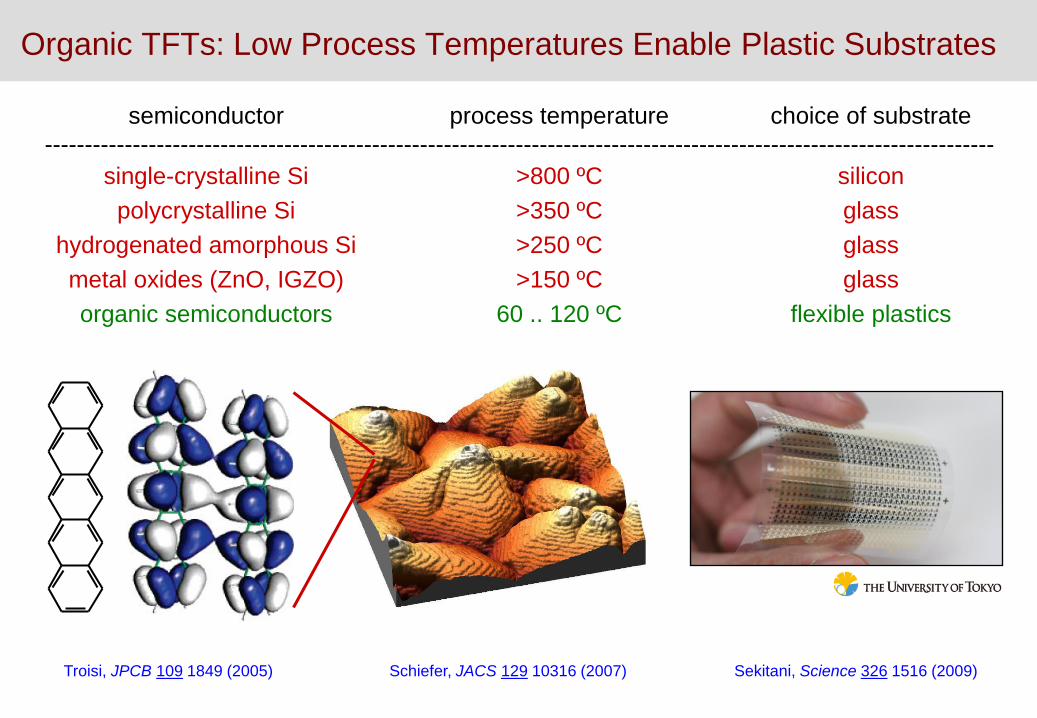
Organic TFTs: Low Process Temperatures Enable Plastic Substrates
semiconductor process temperature choice of substrate
-----------------------------------------------------------------------------------------------------------------------
single-crystalline Si >800 ºC silicon
polycrystalline Si >350 ºC glass
hydrogenated amorphous Si >250 ºC glass
metal oxides (ZnO, IGZO) >150 ºC glass
organic semiconductors 60 .. 120 ºC flexible plastics
Troisi, JPCB 109 1849 (2005) Schiefer, JACS 129 10316 (2007) Sekitani, Science 326 1516 (2009)

Active-Matrix Organic Light-Emitting Diode (AMOLED) Display Layout
~300 µm AMOLED displays require the integration of
organic LEDs with thin-film transistors (TFTs).

Active-Matrix Display Requirements: Dynamic TFT Performance
display # of rows frame row access TFT
resolution (M) rate time cutoff frequency
------------------------------------------------------------------------------------------------------
VGA 480 100 Hz 20 µsec >100 kHz
HD 1080 400 Hz 2 µsec >1 MHz
row
access
time
frame
time
row
= access x # of rows
time
1 2 3
1
N
2
M
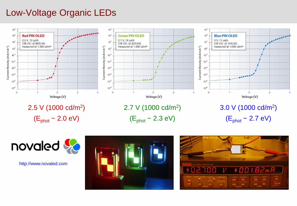
Low-Voltage Organic LEDs
2.5 V (1000 cd/m2)
(Ephot ~ 2.0 eV)
2.7 V (1000 cd/m2)
(Ephot ~ 2.3 eV)
3.0 V (1000 cd/m2)
(Ephot ~ 2.7 eV)
http://www.novaled.com
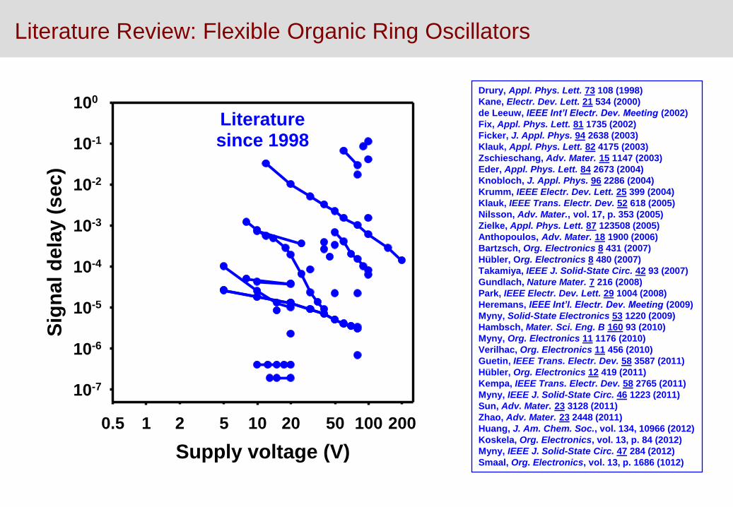
Literature Review: Flexible Organic Ring Oscillators
Drury, Appl. Phys. Lett. 73 108 (1998)
Kane, Electr. Dev. Lett. 21 534 (2000)
de Leeuw, IEEE Int’l Electr. Dev. Meeting (2002)
Fix, Appl. Phys. Lett. 81 1735 (2002)
Ficker, J. Appl. Phys. 94 2638 (2003)
Klauk, Appl. Phys. Lett. 82 4175 (2003)
Zschieschang, Adv. Mater. 15 1147 (2003)
Eder, Appl. Phys. Lett. 84 2673 (2004)
Knobloch, J. Appl. Phys. 96 2286 (2004)
Krumm, IEEE Electr. Dev. Lett. 25 399 (2004)
Klauk, IEEE Trans. Electr. Dev. 52 618 (2005)
Nilsson, Adv. Mater., vol. 17, p. 353 (2005)
Zielke, Appl. Phys. Lett. 87 123508 (2005)
Anthopoulos, Adv. Mater. 18 1900 (2006)
Bartzsch, Org. Electronics 8 431 (2007)
Hübler, Org. Electronics 8 480 (2007)
Takamiya, IEEE J. Solid-State Circ. 42 93 (2007)
Gundlach, Nature Mater. 7 216 (2008)
Park, IEEE Electr. Dev. Lett. 29 1004 (2008)
Heremans, IEEE Int’l. Electr. Dev. Meeting (2009)
Myny, Solid-State Electronics 53 1220 (2009)
Hambsch, Mater. Sci. Eng. B 160 93 (2010)
Myny, Org. Electronics 11 1176 (2010)
Verilhac, Org. Electronics 11 456 (2010)
Guetin, IEEE Trans. Electr. Dev. 58 3587 (2011)
Hübler, Org. Electronics 12 419 (2011)
Kempa, IEEE Trans. Electr. Dev. 58 2765 (2011)
Myny, IEEE J. Solid-State Circ. 46 1223 (2011)
Sun, Adv. Mater. 23 3128 (2011)
Zhao, Adv. Mater. 23 2448 (2011)
Huang, J. Am. Chem. Soc., vol. 134, 10966 (2012)
Koskela, Org. Electronics, vol. 13, p. 84 (2012)
Myny, IEEE J. Solid-State Circ. 47 284 (2012)
Smaal, Org. Electronics, vol. 13, p. 1686 (1012)
Literature summary:Organic ring oscillators
(signal delay vs. supply voltage)flexible
Supply voltage (V)
0.5 2 5 20 50 2001 10 100
Sig
na
l d
ela
y (
se
c)
10-7
10-6
10-5
10-4
10-3
10-2
10-1
100
Literaturesince 1998

Gate Dielectrics: Permittivity, Thickness, Capacitance, Voltage Range
Q V C
(e/cm2) (V) (nF/cm2)
-------------------------------------------
1x10¹³ 20 100
1x10¹³ 3 700
materials ε t C
choice (nm) (nF/cm2)
--------------------------------------------------------------
high-e oxides 16 20 700
thin polymers 3 4 700
Q = V C ε ε0
t C =
Semiconductor
Gate electrode
Gate dielectric
Source Drain
VDS ID
VGS
t
Q ... carrier density in the channel
(target: ~1013 cm-2)
V ... overdrive voltage (VGS-Vth)
C ... gate dielectric capacitance
ε ... gate dielectric permittivity
t ... gate dielectric thickness
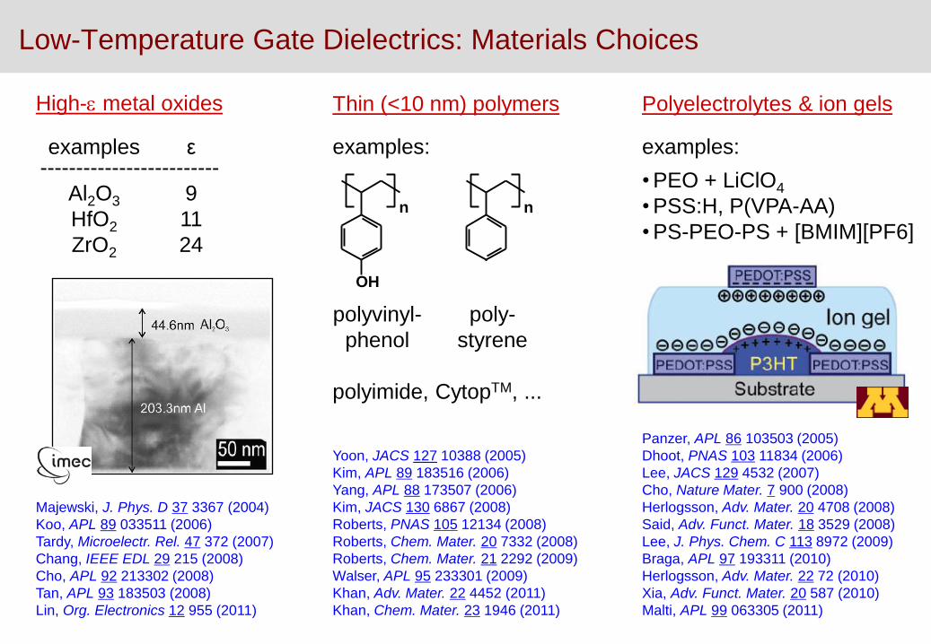
Low-Temperature Gate Dielectrics: Materials Choices
Yoon, JACS 127 10388 (2005)
Kim, APL 89 183516 (2006)
Yang, APL 88 173507 (2006)
Kim, JACS 130 6867 (2008)
Roberts, PNAS 105 12134 (2008)
Roberts, Chem. Mater. 20 7332 (2008)
Roberts, Chem. Mater. 21 2292 (2009)
Walser, APL 95 233301 (2009)
Khan, Adv. Mater. 22 4452 (2011)
Khan, Chem. Mater. 23 1946 (2011)
examples ε -------------------------
Al2O3 9
HfO2 11
ZrO2 24
Majewski, J. Phys. D 37 3367 (2004)
Koo, APL 89 033511 (2006)
Tardy, Microelectr. Rel. 47 372 (2007)
Chang, IEEE EDL 29 215 (2008)
Cho, APL 92 213302 (2008)
Tan, APL 93 183503 (2008)
Lin, Org. Electronics 12 955 (2011)
Thin (<10 nm) polymers
OH
n
polyvinyl-
phenol
poly-
styrene
OH
n
examples:
polyimide, CytopTM, ...
High-e metal oxides Polyelectrolytes & ion gels
Panzer, APL 86 103503 (2005)
Dhoot, PNAS 103 11834 (2006)
Lee, JACS 129 4532 (2007)
Cho, Nature Mater. 7 900 (2008)
Herlogsson, Adv. Mater. 20 4708 (2008)
Said, Adv. Funct. Mater. 18 3529 (2008)
Lee, J. Phys. Chem. C 113 8972 (2009)
Braga, APL 97 193311 (2010)
Herlogsson, Adv. Mater. 22 72 (2010)
Xia, Adv. Funct. Mater. 20 587 (2010)
Malti, APL 99 063305 (2011)
examples:
•PEO + LiClO4
•PSS:H, P(VPA-AA)
•PS-PEO-PS + [BMIM][PF6]

Aluminum Oxide / Self-Assembled Monolayer (SAM) Gate Dielectrics
phosphonic acid
anchor group
aliphatic unit
(6~18 C-atoms)
PO OH
OH
Substrates 22, 28, 31
A = 0.0001 cm2 or 0.0003 cm
2
10 devices each
Bias (V)
-3 -2 -1 0 1 2 3
Cu
rre
nt
de
ns
ity (
A/c
m2)
10-11
10-10
10-9
10-8
10-7
10-6
10-5
10-4
10-3
AlOx + SAM
AlOx only
(4.6 x 10¹⁴ molecules / cm2)
Substrate
Source Drain
Al gate
Organic semiconductor
AlOx (3~4 nm)
SAM (1~2 nm)
Substrate 16
A = 0.126 ... 1.131 cm2
Frequency (Hz)
100 101 102 103 104
Cap
acit
an
ce (
µF
/cm
2)
0.0
0.2
0.4
0.6
0.8
1.0
0.28 cm2
0.50 cm2
0.78 cm2
1.13 cm2
Sekitani et al., Nature Mater. 9 1015 (2010)

Manufacturing Process: Organic TFTs with AlOx/SAM Gate Dielectric
vacuum deposition
of Al gates, Au S/D,
org. semiconductor
plasma oxidation
of Al gate electrodes,
producing 3~4 nm AlOx
Substrate
Source Drain
Al gate electrode
Substrate
Al gate electrode
Substrate
Al gate electrode
Organic semiconductor
SAM
AlOx
Substrate
Al gate electrode
Substrate
Al gate electrode
maximum process temperature: 80 °C

Manufacturing Process: Patterning Using Shadow or Stencil Masks
Source
Drain
1 µm
polyimide
shadow masks
• inexpensive
• easy to use
• poor resolution
silicon
stencil masks
• high resolution
• expensive
• fragile
Source
Drain
Gate
30 µm
30 µm
30 µm

Flexible Pentacene TFTs: Current-Voltage Characteristics
Substrate MPI-32
W = 100 m, L = 50 m
Gate-source voltage (V)
-3 -2 -1 0
Ga
te c
urr
en
t (A
)
10-12
10-11
10-10
10-9
10-8
10-7
10-6
Dra
in c
urr
en
t (A
)
10-12
10-11
10-10
10-9
10-8
10-7
10-6
Drain-source voltage = -1.5 V
Substrate MPI-32
W = 100 m, L = 50 m
Gate-source voltage (V)
-2 -1 0
Ho
le m
ob
ilit
y (
cm
2/V
s)
0.0
0.1
0.2
0.3
0.4Drain-source voltage = -1.5 V
carrier mobility = 0.3 cm2/Vs
on/off current ratio = 105
subthreshold slope = 140 mV/dec
L = 50 µm
W = 100 µm
pentacene
pentacene
Flexible polymeric substrate
Source Drain
Al gate electrode
AlOx/SAM gate dielectric Organic semiconductor
Substrate MPI-32
W = 100 m, L = 50 m
Drain-source voltage (V)
-3 -2 -1 0
Dra
in c
urr
en
t (
A)
-0.4
-0.3
-0.2
-0.1
0.0
Gate-source voltage = -3.0 V
-1.8 V
-2.1 V
-2.4 V
-2.7 V
G
D
S

Pentacene: Rapid Air-Induced Oxidation and Loss of Conjugation
de Angelis, Chem. Phys. Lett. 468 193 (2009)
pentacene
O
O
air
Substrates MPI-122, MPI-144, MPI-285 (pentacene)
Exposure to air (days)
0 30 60 90 120
Ho
le m
ob
ilit
y (
cm
2/V
s)
0.0
0.1
0.2
0.3
0.4
0.5stored andtested in air
pentacene
Qiu, Appl. Phys. Lett. 83 1644 (2003)
Lee, Synth. Metals 143 21 (2004)
Kim, J. Vac. Sci. Technol. B 23 2357 (2005)
Han, Appl. Phys. Lett. 88 073519 (2006)
Sekitani, Jpn. J. Appl. Phys. 46 4300 (2007)
Ashimine, Jpn. J. Appl. Phys. 47 1760 (2008)
Jeon, Appl. Phys. Lett. 93 163304 (2008)
Jung, Appl. Phys. Lett. 92 163504 (2008)
Yang, J. Phys. Chem. C 112 16161 (2008)
after 240 days
in air
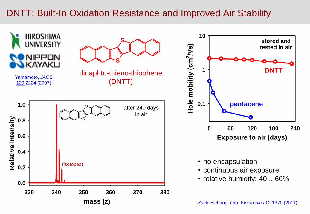
DNTT: Built-In Oxidation Resistance and Improved Air Stability
DNTT mass spectrogram(after 240 days in air)
mass (z)
330 340 350 360 370 380
Re
lati
ve
in
ten
sit
y
0.0
0.2
0.4
0.6
0.8
1.0
S
S
dinaphto-thieno-thiophene
(DNTT) Yamamoto, JACS
129 2224 (2007)
Substrate MPI-479 (DNTT, W = 100 m, L = 50 m)Substrates MPI-122, MPI-144, MPI-285 (pentacene)
Exposure to air (days)
0 60 120 180 240
Ho
le m
ob
ilit
y (
cm
2/V
s)
0.1
1
10stored andtested in air
pentacene
DNTT
S
S
(isotopes)
after 240 days
in air
• no encapsulation
• continuous air exposure
• relative humidity: 40 .. 60%
Zschieschang, Org. Electronics 12 1370 (2011)

Flexible DNTT TFTs: Current-Voltage Characteristics
Flexible polymeric substrate
Source Drain
Al gate electrode
AlOx/SAM gate dielectric Organic semiconductor
G
D
S
Substrate MPI-479
W = 100 m, L = 30 m
Gate-source voltage (V)
-2 -1 0
Ho
le m
ob
ilit
y (
cm
2/V
s)
0
1
2
3Drain-source voltage = -1.5 V
L = 30 µm
W = 100 µm
Substrate MPI-479
W = 100 m, L = 30 m
Drain-source voltage (V)
-3 -2 -1 0
Dra
in c
urr
en
t (
A)
-10
-8
-6
-4
-2
0
Gate-source voltage = -3.0 V
-1.8 V
-2.1 V
-2.4 V
-2.7 V
Substrate MPI-479
W = 100 m, L = 30 m
Gate-source voltage (V)
-3 -2 -1 0
Ga
te c
urr
en
t (A
)
10-13
10-12
10-11
10-10
10-9
10-8
10-7
10-6
10-5
Dra
in c
urr
en
t (A
)
10-13
10-12
10-11
10-10
10-9
10-8
10-7
10-6
10-5
Drain-sourcevoltage = -1.5 V
S
S
DNTT
carrier mobility = 2.4 cm2/Vs
on/off current ratio = 107
subthreshold slope = 110 mV/dec
Zschieschang, Org. Electronics 12 1370 (2011)

Low-Voltage Organic TFTs: Controlling Large-Area Organic LEDs
VGS = -3.5 V
ILED = 67 µA
VGS = -2.5 V
ILED = 25 µA
VGS = -2.0 V
ILED = 10 µA
-5 V
IOLED
Substrate MPI-654
W = 200 m, L = 10 m
Gate-source voltage (V)
-3 -2 -1 0
OL
ED
dri
ve
cu
rre
nt
(A)
10-11
10-10
10-9
10-8
10-7
10-6
10-5
10-4
0 V
-3.5 V
L = 10 µm
W = 200 µm
2.6 mm
2.6
mm
Zschieschang, Org. Electronics
12 1370 (2011)
VGS = -3.0 V
ILED = 46 µA
S
S

Low-Voltage Organic TFTs and Circuits on Banknotes
Zschieschang, Adv. Mater. 23 654 (2011)
Substrate MPI-307 (5-Euro bill)DNTT TFTs
W = 100 m, L = 30 m
Gate-source voltage (V)
-3 -2 -1 0
Gate
cu
rren
t (A
)
10-12
10-11
10-10
10-9
10-8
10-7
10-6
Dra
in c
urr
en
t (A
)
10-12
10-11
10-10
10-9
10-8
10-7
10-6
92 TFTs
L = 30 m
W = 100 m
Substrate MPI-253 (5-Euro bill)
W = 100 m, L = 15 m
Drain-source voltage (V)
-3 -2 -1 0
Dra
in c
urr
en
t (
A)
-1.2
-0.9
-0.6
-0.3
0.0
Gate-source voltage = -3.0 V
-1.8 V
-2.1 V
-2.4 V
-2.7 V

Relationship Between Intermolecular Distance and Carrier Mobility
Troisi,
J. Phys. Chem. B
109 1849 (2005)
SS
SS
SS
SS
distance
Bredas,
Proc. Nat’l. Acad. Sci.
99 5804 (2002)
d ~ 0.7 nm
Kang,
Adv. Mater.
23 1222 (2011)
increased van-der-Waals interactions
smaller intermolecular distance
improved orbital overlap
larger carrier mobility
dialkyl-DNTT DNTT
Yamamoto,
J. Am. Chem. Soc.
129 2224 (2007)
orbital
overlap

Flexible C10-DNTT TFTs: Current-Voltage Characteristics
carrier mobility = 4.3 cm2/Vs
on/off current ratio = 108
subthreshold slope = 68 mV/dec L = 30 µm
W = 100 µm
Substrate MPI-1120
W = 100 m, L = 30 m
Drain-source voltage (V)
-3 -2 -1 0
Dra
in c
urr
en
t (
A)
-15
-12
-9
-6
-3
0
Gate-source voltage = -2.0 V
-1.2 V
-1.4 V
-1.6 V
-1.8 V
Substrate MPI-1120
W = 100 m, L = 30 m
Gate-source voltage (V)
-2 -1 0
Gate
cu
rren
t (A
)
10-14
10-13
10-12
10-11
10-10
10-9
10-8
10-7
10-6
10-5
Dra
in c
urr
en
t (A
)
10-14
10-13
10-12
10-11
10-10
10-9
10-8
10-7
10-6
10-5Drain-sourcevoltage = -2.0 V
C10-DNTT
S
S C10H21
H21C10
Flexible polymeric substrate
Source Drain
Al gate electrode
AlOx/SAM gate dielectric Organic semiconductor
Substrate MPI-1120
W = 100 m, L = 30 m
Gate-source voltage (V)
-2 -1 0
Ho
le m
ob
ilit
y (
cm
2/V
s)
0
1
2
3
4
5Drain-source voltage = -2.0 V
Zschieschang, J. Mater. Chem. 22 4273 (2012)
G
D
S

S
S C10H21
H21C10
Dynamic TFT Performance: Theoretical Prediction
fT ~ µ VDS
2π L (L + 2L)
µ ~ 4 cm2/Vs
VDS ~ 2 V
Source
Drain
Gate
polyimide shadow masks:
L ~ 30 µm
L ~ 30 µm
fT ~ 50 kHz
(2fT)-1 ~ 10 µsec
30 µm
30 µm
30 µm
display # of rows frame row access TFT
resolution (M) rate time cutoff frequency
------------------------------------------------------------------------------------------------------
VGA 480 100 Hz 20 µsec >100 kHz
HD 1080 400 Hz 2 µsec >1 MHz
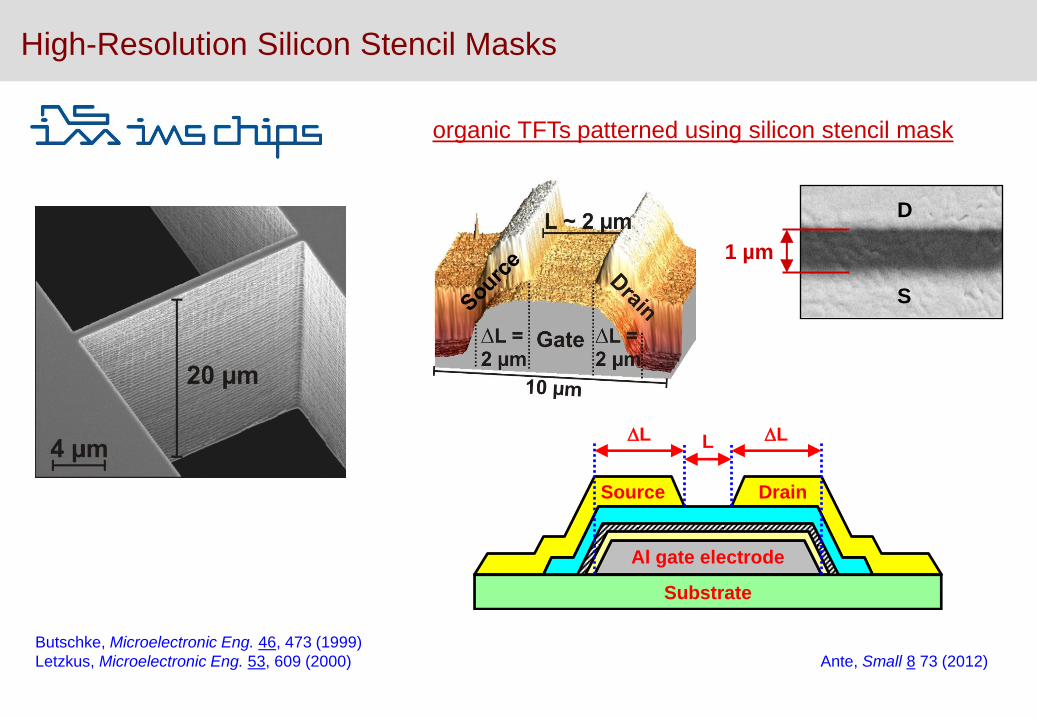
High-Resolution Silicon Stencil Masks
organic TFTs patterned using silicon stencil mask
Butschke, Microelectronic Eng. 46, 473 (1999)
Letzkus, Microelectronic Eng. 53, 609 (2000) Ante, Small 8 73 (2012)
S
D
1 µm
Substrate
Source Drain
Al gate electrode
L L L
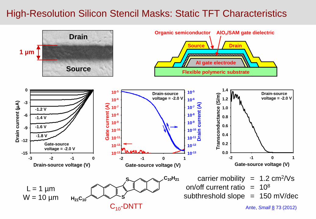
High-Resolution Silicon Stencil Masks: Static TFT Characteristics
L = 1 µm
W = 10 µm
Source
Drain
1 µm
carrier mobility = 1.2 cm2/Vs
on/off current ratio = 108
subthreshold slope = 150 mV/dec
Ante, Small 8 73 (2012)
Substrate MPI-1294C10-DNTT/DNTT TFT on PEN
W = 10 m, L = 1 m
Gate-source voltage (V)
-2 -1 0 1
Gate
cu
rren
t (A
)
10-13
10-12
10-11
10-10
10-9
10-8
10-7
10-6
10-5
Dra
in c
urr
en
t (A
)
10-13
10-12
10-11
10-10
10-9
10-8
10-7
10-6
10-5Drain-sourcevoltage = -2.0 V
Substrate MPI-1294C10-DNTT/DNTT TFT on PEN
W = 10 m, L = 1 m
Drain-source voltage (V)
-3 -2 -1 0
Dra
in c
urr
en
t (
A)
-15
-12
-9
-6
-3
0
Gate-source voltage = -2.0 V
-1.2 V
-1.4 V
-1.6 V
-1.8 V
C10-DNTT
S
S C10H21
H21C10
Flexible polymeric substrate
Source Drain
Al gate electrode
AlOx/SAM gate dielectric Organic semiconductor
Substrate MPI-1294C10-DNTT/DNTT TFT on PEN
W = 10 m, L = 1 m
Gate-source voltage (V)
-2 -1 0 1
Tra
nsc
on
du
cta
nc
e (
S/m
)
0.0
0.2
0.4
0.6
0.8
1.0
1.2
1.4Drain-source voltage = -2.0 V

High-Resolution Silicon Stencil Masks: TFT Parameter Uniformity
carrier mobility = 1.2 cm2/Vs
on/off current ratio = 107
subthreshold slope = 150 mV/dec
Ante, Small 8 73 (2012)
Substrate MPI-1294
W = 10 m, L = 1 m16 C10-DNTT TFTs on PEN, fresh
Transconductance (S/m)
0.0 0.5 1.0 1.5 2.0
Co
un
ts
0
1
2
3
4
5
6
7
8
9mean = 1.2 S/m
= 0.078 S/m (6%)
L = 1 µm
W = 10 µm
C10-DNTT
S
S C10H21
H21C10
Substrate MPI-1294
W = 10 m, L = 1 m16 C10-DNTT TFTs on PEN, fresh
Gate-source voltage (V)
-2 -1 0
Dra
in c
urr
en
t (A
)
10-13
10-12
10-11
10-10
10-9
10-8
10-7
10-6
10-5Drain-source voltage = -2.0 V
16 TFTs
L = 1 m
W = 10 m

S
S C10H21
H21C10
Dynamic TFT Performance: Theoretical Prediction
fT ~ µ VDS
2π L (L + 2L)
µ ~ 4 cm2/Vs
VDS ~ 2 V
Source
Drain
Gate
polyimide shadow masks:
L ~ 30 µm
L ~ 30 µm
fT ~ 50 kHz
(2fT)-1 ~ 10 µsec
30 µm
30 µm
30 µm
silicon stencil masks:
L ~ 1 µm
L ~ 5 µm
fT ~ 5 MHz
(2fT)-1 ~ 100 nsec Source
Drain
1 µm

Dynamic TFT Performance: Experimental Ring Oscillator Delay
fT ~ µ VDS
2π L (L + 2L)
µ ~ 4 cm2/Vs
VDS ~ 2 V
Zschieschang, J. Mater. Chem. 22 4273 (2012)
Ante, Small 8 73 (2012)
S
S C10H21
H21C10
polyimide shadow masks:
L ~ 30 µm
L ~ 30 µm
fT ~ 50 kHz
(2fT)-1 ~ 10 µsec
silicon stencil masks:
L ~ 1 µm
L ~ 5 µm
fT ~ 5 MHz
(2fT)-1 ~ 100 nsec
MPI-1120 (C10-DNTT, flexible PEN, L = 30 µm)MPI-1150 (C10-DNTT, flexible PEN, L = 1 µm)
Supply voltage (V)
1 2 3 4
Sig
nal d
ela
y p
er
sta
ge (
sec)
10-7
10-6
10-5
10-4
L = 1 m, L = 5 m(420 ns @ 3 V)
L = L = 30 m
(25 s @ 3 V)

Literature Comparison: Flexible Organic Ring Oscillators
Drury, Appl. Phys. Lett. 73 108 (1998)
Kane, Electr. Dev. Lett. 21 534 (2000)
de Leeuw, IEEE Int’l Electr. Dev. Meeting (2002)
Fix, Appl. Phys. Lett. 81 1735 (2002)
Ficker, J. Appl. Phys. 94 2638 (2003)
Klauk, Appl. Phys. Lett. 82 4175 (2003)
Zschieschang, Adv. Mater. 15 1147 (2003)
Eder, Appl. Phys. Lett. 84 2673 (2004)
Knobloch, J. Appl. Phys. 96 2286 (2004)
Krumm, IEEE Electr. Dev. Lett. 25 399 (2004)
Klauk, IEEE Trans. Electr. Dev. 52 618 (2005)
Nilsson, Adv. Mater., vol. 17, p. 353 (2005)
Zielke, Appl. Phys. Lett. 87 123508 (2005)
Anthopoulos, Adv. Mater. 18 1900 (2006)
Bartzsch, Org. Electronics 8 431 (2007)
Hübler, Org. Electronics 8 480 (2007)
Takamiya, IEEE J. Solid-State Circ. 42 93 (2007)
Gundlach, Nature Mater. 7 216 (2008)
Park, IEEE Electr. Dev. Lett. 29 1004 (2008)
Heremans, IEEE Int’l. Electr. Dev. Meeting (2009)
Myny, Solid-State Electronics 53 1220 (2009)
Hambsch, Mater. Sci. Eng. B 160 93 (2010)
Myny, Org. Electronics 11 1176 (2010)
Verilhac, Org. Electronics 11 456 (2010)
Guetin, IEEE Trans. Electr. Dev. 58 3587 (2011)
Hübler, Org. Electronics 12 419 (2011)
Kempa, IEEE Trans. Electr. Dev. 58 2765 (2011)
Myny, IEEE J. Solid-State Circ. 46 1223 (2011)
Sun, Adv. Mater. 23 3128 (2011)
Zhao, Adv. Mater. 23 2448 (2011)
Huang, J. Am. Chem. Soc., vol. 134, 10966 (2012)
Koskela, Org. Electronics, vol. 13, p. 84 (2012)
Myny, IEEE J. Solid-State Circ. 47 284 (2012)
Smaal, Org. Electronics, vol. 13, p. 1686 (1012)
Literature summary:Organic ring oscillators
(signal delay vs. supply voltage)flexible
Supply voltage (V)
0.5 2 5 20 50 2001 10 100
Sig
na
l d
ela
y (
se
c)
10-7
10-6
10-5
10-4
10-3
10-2
10-1
100
Literaturesince 1998
L = 1 m
L = 10 m

Active-Matrix Displays: External Row and Column Drivers
Ro
w S
hif
t R
eg
iste
r
Digital/Analog Converter
Latch
Column Shift Register
data
clock
clock

Rollable Active-Matrix Displays with Integrated Row Drivers
http://www.sony.net/SonyInfo/News/Press/201005/10-070E/index.html
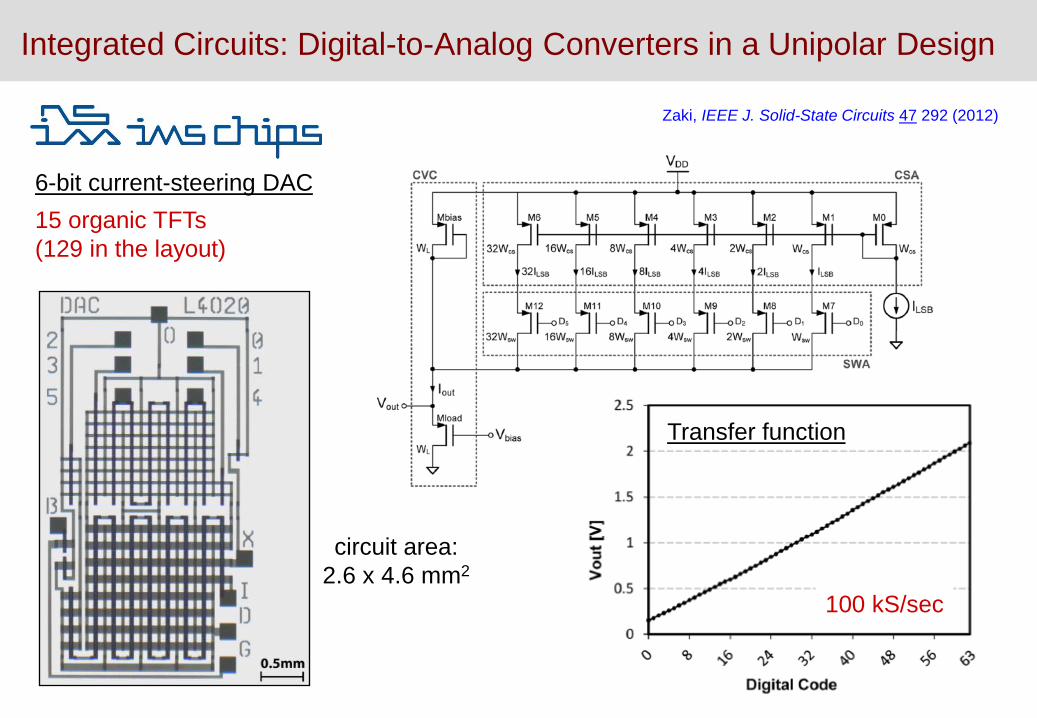
Integrated Circuits: Digital-to-Analog Converters in a Unipolar Design
6-bit current-steering DAC
15 organic TFTs
(129 in the layout)
circuit area:
2.6 x 4.6 mm2
Transfer function
Zaki, IEEE J. Solid-State Circuits 47 292 (2012)
100 kS/sec

Comparison: Unipolar vs. Complementary Logic
complementary
p-channel TFT
VDD
input
output
n-channel TFT
VDD
input
output
p-channel TFT
p-channel TFT
unipolar
Substrate MPI-248Inverter with saturated load
Wdrive
= 100 µm, Ldrive
= 10 µm, Wload
= 50 µm, Lload
= 100 µm
Ou
tpu
t vo
ltag
e (
V)
-3
-2
-1
0
Cu
rren
t (A
)
10-10
10-9
10-8
10-7
10-6
10-5
10-4
10-3
10-2
Input voltage (V)
-3 -2 -1 0
Gain
0
1
2
VDD
= -3 V
Substrate MPI-28850% C18H37-PA, 50% C18H22F15-PA
Complementary inverterW
p = 100 µm, L
p = 30 µm, W
n = 1000 µm, L
n = 30 µm
Ou
tpu
t vo
ltag
e (
V)
0
1
2
Cu
rren
t (A
)
10-13
10-12
10-11
10-10
10-9
10-8
10-7
10-6
10-5
10-4
10-3
Input voltage (V)
0 1 2
Gain
0
200
400
VDD
= 2 V

Semiconductors for n-Channel TFTs: Orbital Energy Considerations
Au
p-channel TFT
(air-stable)
HOMO ~ 5 eV
Au
n-channel TFT
(air-stable)
LUMO ~ 4.5 eV
NN
N
N
Cu
NN
N N
F F
FF
F
F
F
F
F
FF
F
F
F
F
F
F16CuPc
S
S C10H21
H21C10
S
S
HOMO ~ 6.3 eV
LUMO ~ 2 eV
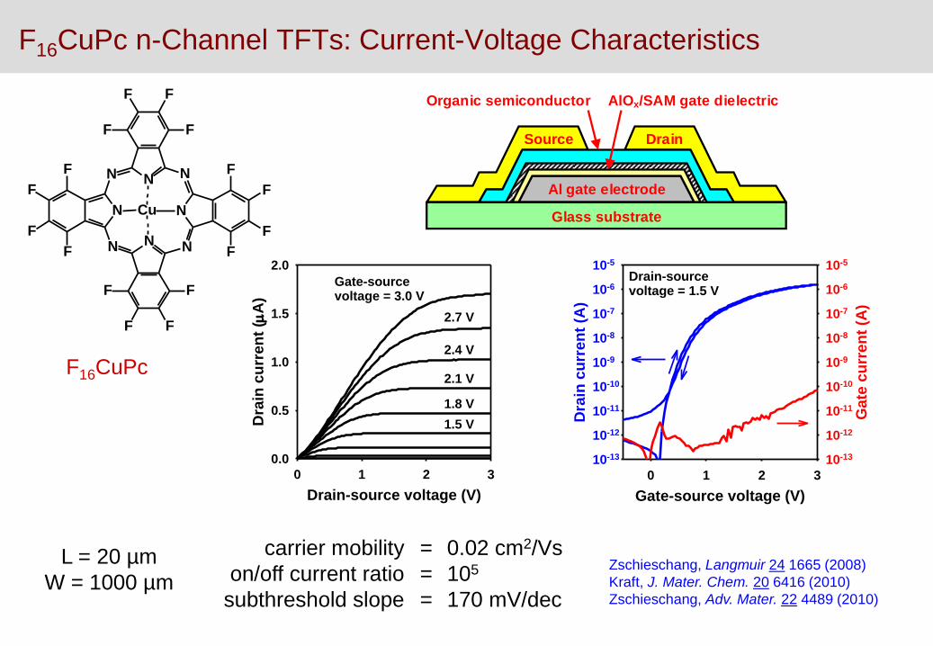
F16CuPc n-Channel TFTs: Current-Voltage Characteristics
Substrate MPI-411
W = 1000 m, L = 20 m
Drain-source voltage (V)
0 1 2 3
Dra
in c
urr
en
t (
A)
0.0
0.5
1.0
1.5
2.0
Gate-source voltage = 3.0 V
2.1 V
1.5 V
2.4 V
1.8 V
2.7 V
Substrate MPI-411
W = 1000 m, L = 20 m
Gate-source voltage (V)
0 1 2 3
Dra
in c
urr
en
t (A
)
10-13
10-12
10-11
10-10
10-9
10-8
10-7
10-6
10-5
Ga
te c
urr
en
t (A
)
10-13
10-12
10-11
10-10
10-9
10-8
10-7
10-6
10-5
Drain-source voltage = 1.5 V
N
N N N
N
NNN
Cu
F
F
F
F
F
F F
F
F
F
F
F
F
F
F
F
F16CuPc
Glass substrate
Source Drain
Al gate electrode
AlOx/SAM gate dielectric Organic semiconductor
L = 20 µm
W = 1000 µm
carrier mobility = 0.02 cm2/Vs
on/off current ratio = 105
subthreshold slope = 170 mV/dec
Zschieschang, Langmuir 24 1665 (2008)
Kraft, J. Mater. Chem. 20 6416 (2010)
Zschieschang, Adv. Mater. 22 4489 (2010)

Organic Complementary Inverters: Static Performance
p-channel TFT
VDD
input
output
n-channel TFT
Substrate MPI-28850% C18H37-PA, 50% C18H22F15-PA
Complementary inverterW
p = 100 µm, L
p = 30 µm, W
n = 1000 µm, L
n = 30 µm
Ou
tpu
t v
olt
ag
e (
V)
0
1
2
Cu
rre
nt
(A)
10-13
10-12
10-11
10-10
10-9
10-8
10-7
10-6
10-5
10-4
10-3
Input voltage (V)
0 1 2
Ga
in
0
200
400
VDD
= 2 V
N
N N N
N
NNN
Cu
F
F
F
F
F
F F
F
F
F
F
F
F
F
F
F
pentacene
F16CuPc
• large output swing (= VDD)
• small static currents (<10 pA)
• large gain (>200)
Substrate
Gate (Al) Gate (Al)
S D D S
Semiconductor for p-channel TFT
Semiconductor for n-channel TFT
AlOx/SAM gate dielectric
Zschieschang, Adv. Mater. 22 4489 (2010)

Organic Complementary Ring Oscillators: Dynamic Performance
VDD
silicon stencil masks (L = 1 µm)
polyimide shadow masks (L = 20 µm)
Zschieschang, Adv. Mater. 22 4489 (2010)
Ante, Int’l Electron Devices Meeting (2010)
MPI-288 (complementary, 20 µm, mixed C18-PA SAM)Stencil-9 (complementary, 20 µm, 5 µm, 1 µm)
Supply voltage (V)
1 2 3
Sig
na
l d
ela
y p
er
sta
ge
(s
ec
)
10-5
10-4
10-3
10-2
10-1
100
L = 1 m, L = 2 m
(63 s @ 3 V)
L = L = 20 m(3.3 ms @ 3 V)

F16CuPc n-Channel TFTs: Current-Voltage Characteristics
Substrate MPI-411
W = 1000 m, L = 20 m
Drain-source voltage (V)
0 1 2 3
Dra
in c
urr
en
t (
A)
0.0
0.5
1.0
1.5
2.0
Gate-source voltage = 3.0 V
2.1 V
1.5 V
2.4 V
1.8 V
2.7 V
Substrate MPI-411
W = 1000 m, L = 20 m
Gate-source voltage (V)
0 1 2 3
Dra
in c
urr
en
t (A
)
10-13
10-12
10-11
10-10
10-9
10-8
10-7
10-6
10-5
Ga
te c
urr
en
t (A
)
10-13
10-12
10-11
10-10
10-9
10-8
10-7
10-6
10-5
Drain-source voltage = 1.5 V
N
N N N
N
NNN
Cu
F
F
F
F
F
F F
F
F
F
F
F
F
F
F
F
F16CuPc
Glass substrate
Source Drain
Al gate electrode
AlOx/SAM gate dielectric Organic semiconductor
L = 20 µm
W = 1000 µm
carrier mobility = 0.02 cm2/Vs
on/off current ratio = 105
subthreshold slope = 170 mV/dec
Zschieschang, Langmuir 24 1665 (2008)
Kraft, J. Mater. Chem. 20 6416 (2010)
Zschieschang, Adv. Mater. 22 4489 (2010)
Semiconductors for High-Mobility Air-Stable Organic n-Channel TFTs
N
N
OO
OO
F2C
CF2
F3C
CF2
F2CCF3
0.12 cm2/Vs 1.2 cm2/Vs
N
N
OO
O O
Cl
Cl
F2C
CF2
F3C
CF2
F2CCF3
1.3 cm2/Vs
N
N
OO
OO
CN
NC
F2C
CF2
F3C
CF2
F2CCF3
0.64 cm2/Vs
Katz, J. Am. Chem. Soc.
122 7787 (2000)
N OO
F2C
CF2
F3C
N OO
CF2
F2CCF3
Jones, Angew. Chem. Int. Ed.
43 6363 (2004)
Schmidt, J. Am. Chem. Soc.
131 6215 (2009)
Oh, Adv. Funct. Mater.
20 2148 (2010)

Air-Stable Organic n-Channel TFTs: Current-Voltage Characteristics
N
N
OO
O O
Cl
Cl
F2C
CF2
F3C
CF2
F2CCF3
L = 100 µm
W = 200 µm
ALD AlOx/SAM
Au source Au drain
Gate dielectric (100 nm thermal SiO2)
Heavily doped silicon wafer
Organic semiconductor
carrier mobility = 1.4 cm2/Vs
on/off current ratio = 107
subthreshold slope = 1.1 V/dec
Substrate MPI-780
W = 200 m, L = 100 mfresh
Drain-source voltage (V)
0 10 20 30 40
Dra
in c
urr
en
t (
A)
0
5
10
15
20Gate-source voltage = 35 V
25 V
30 V
20 V
Substrate MPI-780
W = 200 m, L = 100 mfresh
Gate-source voltage (V)
-10 0 10 20 30 40
Dra
in c
urr
en
t (A
)
10-13
10-12
10-11
10-10
10-9
10-8
10-7
10-6
10-5
Gate
cu
rren
t (A
)
10-13
10-12
10-11
10-10
10-9
10-8
10-7
10-6
10-5Drain-source voltage = 50 V
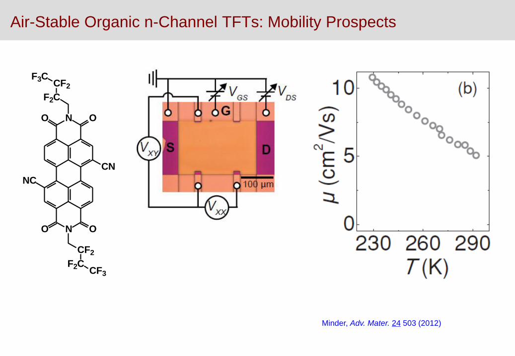
Air-Stable Organic n-Channel TFTs: Mobility Prospects
Minder, Adv. Mater. 24 503 (2012)
N
N
OO
OO
CN
NC
F2C
CF2
F3C
CF2
F2CCF3

Summary
• Organic thin-film transistors that can be fabricated at
low temperatures (<100 ºC) and can be operated with
low voltages (~3 V) are useful for flexible displays.
• Low-temperature processing and low-voltage operation
are enabled by hybrid gate dielectrics based on
a plasma-grown metal oxide (~4 nm AlOx) and
a molecular self-assembled monolayer (~2 nm).
• Improved air stability is enabled by organic
semiconductors with greater oxidation resistance.
• Low-voltage organic TFTs have cutoff frequencies
between 10 kHz and 4 MHz, depending on the
lateral dimensions (~1 to 20 µm).
• Complementary circuits based on organic TFTs
are useful to integrate the row and column drivers
on the flexible display backplane.
PO OH
OH
S
S