
Low-Voltage Analog CMOS Architectures and Design Methods
161
Brigham Young University Brigham Young University BYU ScholarsArchive BYU ScholarsArchive Theses and Dissertations 2007-11-16 Low-Voltage Analog CMOS Architectures and Design Methods Low-Voltage Analog CMOS Architectures and Design Methods Kent Downing Layton Brigham Young University - Provo Follow this and additional works at: https://scholarsarchive.byu.edu/etd Part of the Electrical and Computer Engineering Commons BYU ScholarsArchive Citation BYU ScholarsArchive Citation Layton, Kent Downing, "Low-Voltage Analog CMOS Architectures and Design Methods" (2007). Theses and Dissertations. 1218. https://scholarsarchive.byu.edu/etd/1218 This Dissertation is brought to you for free and open access by BYU ScholarsArchive. It has been accepted for inclusion in Theses and Dissertations by an authorized administrator of BYU ScholarsArchive. For more information, please contact [email protected], [email protected].
Transcript of Low-Voltage Analog CMOS Architectures and Design Methods

Brigham Young University Brigham Young University
BYU ScholarsArchive BYU ScholarsArchive
Theses and Dissertations
2007-11-16
Low-Voltage Analog CMOS Architectures and Design Methods Low-Voltage Analog CMOS Architectures and Design Methods
Kent Downing Layton Brigham Young University - Provo
Follow this and additional works at: https://scholarsarchive.byu.edu/etd
Part of the Electrical and Computer Engineering Commons
BYU ScholarsArchive Citation BYU ScholarsArchive Citation Layton, Kent Downing, "Low-Voltage Analog CMOS Architectures and Design Methods" (2007). Theses and Dissertations. 1218. https://scholarsarchive.byu.edu/etd/1218
This Dissertation is brought to you for free and open access by BYU ScholarsArchive. It has been accepted for inclusion in Theses and Dissertations by an authorized administrator of BYU ScholarsArchive. For more information, please contact [email protected], [email protected].

LOW-VOLTAGE ANALOG CMOS ARCHITECTURES
AND DESIGN METHODS
by
Kent D. Layton
A dissertation submitted to the faculty of
Brigham Young University
in partial fulfillment of the requirements for the degree of
Doctor of Philosophy
Department of Electrical and Computer Engineering
Brigham Young University
December 2007


Copyright c© 2007 Kent D. Layton
All Rights Reserved


BRIGHAM YOUNG UNIVERSITY
GRADUATE COMMITTEE APPROVAL
of a dissertation submitted by
Kent D. Layton
This dissertation has been read by each member of the following graduate committeeand by majority vote has been found to be satisfactory.
Date Donald T. Comer, Chair
Date David J. Comer
Date Richard H. Selfridge
Date Michael A. Jensen
Date Doran K. Wilde


BRIGHAM YOUNG UNIVERSITY
As chair of the candidate’s graduate committee, I have read the dissertation of KentD. Layton in its final form and have found that (1) its format, citations, and bibli-ographical style are consistent and acceptable and fulfill university and departmentstyle requirements; (2) its illustrative materials including figures, tables, and chartsare in place; and (3) the final manuscript is satisfactory to the graduate committeeand is ready for submission to the university library.
Date Donald T. ComerChair, Graduate Committee
Accepted for the Department
Michael J. WirthlinGraduate Coordinator
Accepted for the College
Alan R. ParkinsonDean, Ira A. Fulton College ofEngineering and Technology


ABSTRACT
LOW-VOLTAGE ANALOG CMOS ARCHITECTURES
AND DESIGN METHODS
Kent D. Layton
Department of Electrical and Computer Engineering
Doctor of Philosophy
This dissertation develops design methods and architectures which allow ana-
log circuits to operate at VT + 2Vds,sat, the minimum supply for CMOS circuits with
all transistors in the active region where Vds,sat is the drain to source saturation volt-
age of a MOS transistor. Techniques which meet this criteria for rail-to-rail input
stages, gain enhancement stages, and output stages are discussed and developed.
These techniques are used to design four fully-differential rail-to-rail amplifiers. The
highest gain is shown to be attained using a drain voltage equalization (DVE) or
active-bootstrapping technique which produces more than 100dB of gain in a two
stage amplifier with a bulk-driven input pair while showing no bandwidth degrada-
tion when compared to amplifier architectures with similar biasing. The low voltage
design techniques are extended to switching and sampling circuits. A 10-bit digi-
tal to analog converter (DAC) and a 10-bit analog to digital converter (ADC) are
designed and fabricated in a 0.35µm dual-well CMOS process to prove the devel-
oped design methods, architectures, and techniques. The 10-bit DAC operates at

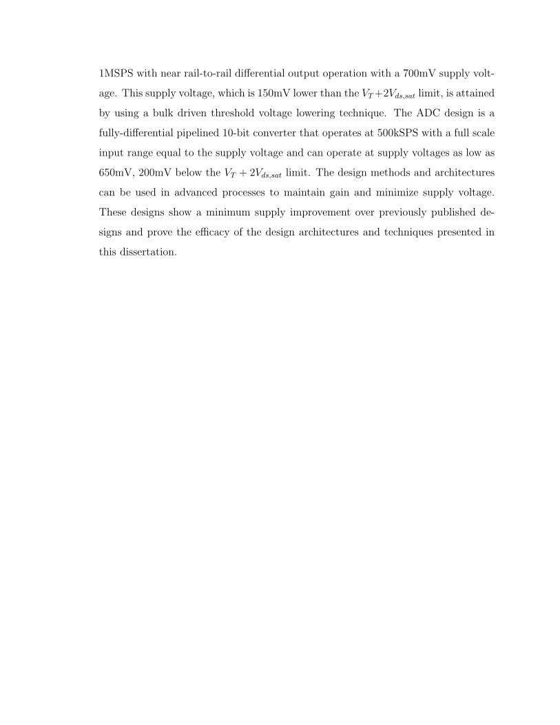
1MSPS with near rail-to-rail differential output operation with a 700mV supply volt-
age. This supply voltage, which is 150mV lower than the VT +2Vds,sat limit, is attained
by using a bulk driven threshold voltage lowering technique. The ADC design is a
fully-differential pipelined 10-bit converter that operates at 500kSPS with a full scale
input range equal to the supply voltage and can operate at supply voltages as low as
650mV, 200mV below the VT + 2Vds,sat limit. The design methods and architectures
can be used in advanced processes to maintain gain and minimize supply voltage.
These designs show a minimum supply improvement over previously published de-
signs and prove the efficacy of the design architectures and techniques presented in
this dissertation.


ACKNOWLEDGMENTS
I would like to acknowledge the efforts of the many other people who made
this dissertation a reality. I thank Dr. Don Comer for his efforts as my instructor,
mentor, and committee chairman. I am grateful to Dr. David Comer for his timely
and informative feedback on my papers and research. I would also like to thank Dr.
Michael Jensen, Dr. Richard Selfridge, and Dr. Doran Wilde for their support and
input on this dissertation. I am grateful for the time and support that my co-workers
gave in reading many versions of my research papers and helping to test the silicon
results.
Most importantly, I would like to thank my wife, Heidi, for her support and
drive in completing this dissertation. I am indebted to my parents for raising me with
a high regard for education and prodding me to continue my studies. Finally, I must
acknowledge the efforts of my son, Luke, who added many keystrokes to this work
even though the majority of them were modified.


Table of Contents
Acknowledgements xiii
List of Tables xix
List of Figures xxv
1 Introduction 1
1.1 Low Voltage Amplifiers . . . . . . . . . . . . . . . . . . . . . . . . . . 3
1.2 Analog Systems . . . . . . . . . . . . . . . . . . . . . . . . . . . . . . 5
1.3 Contributions of this Work . . . . . . . . . . . . . . . . . . . . . . . . 6
2 Threshold Voltage and Input Architectures 9
2.1 MOS Differential Input Pair . . . . . . . . . . . . . . . . . . . . . . . 9
2.2 Supply Voltage Boosting . . . . . . . . . . . . . . . . . . . . . . . . . 10
2.3 Threshold Shifting . . . . . . . . . . . . . . . . . . . . . . . . . . . . 11
2.3.1 Depletion Mode Transistors . . . . . . . . . . . . . . . . . . . 12
2.3.2 Floating-Gate Transistors . . . . . . . . . . . . . . . . . . . . 12
2.3.3 Bulk Driven Theshold Reduction . . . . . . . . . . . . . . . . 14
2.4 Signal Shifting . . . . . . . . . . . . . . . . . . . . . . . . . . . . . . . 16
2.4.1 Capacitive Signal Shifting . . . . . . . . . . . . . . . . . . . . 16
2.4.2 Resistive Level Shifting . . . . . . . . . . . . . . . . . . . . . . 17
2.5 Bulk-Driven Transistors . . . . . . . . . . . . . . . . . . . . . . . . . 19
xv

2.6 Pseudo-Differential Inputs . . . . . . . . . . . . . . . . . . . . . . . . 21
2.7 Summary . . . . . . . . . . . . . . . . . . . . . . . . . . . . . . . . . 21
3 Gain Enhancement 23
3.1 Transconductance Enhancement . . . . . . . . . . . . . . . . . . . . . 25
3.2 Output Impedance Enhancement . . . . . . . . . . . . . . . . . . . . 26
3.2.1 Cascode . . . . . . . . . . . . . . . . . . . . . . . . . . . . . . 26
3.2.2 Cascode Architectures in Low Voltage Design . . . . . . . . . 28
3.2.3 Current Stealing . . . . . . . . . . . . . . . . . . . . . . . . . 30
3.2.4 Positive Feedback . . . . . . . . . . . . . . . . . . . . . . . . . 32
3.2.5 Partial Positive Feedback . . . . . . . . . . . . . . . . . . . . . 34
3.2.6 Drain Voltage Equalization and Active Bootstrapping . . . . . 36
3.3 Conclusion . . . . . . . . . . . . . . . . . . . . . . . . . . . . . . . . . 43
4 Output Stages 45
4.1 Class-AB Output Stages . . . . . . . . . . . . . . . . . . . . . . . . . 46
4.1.1 Capacitive Biasing . . . . . . . . . . . . . . . . . . . . . . . . 47
4.1.2 Two Stage Biasing . . . . . . . . . . . . . . . . . . . . . . . . 47
4.1.3 Resistive Level Shifting . . . . . . . . . . . . . . . . . . . . . . 49
4.2 Summary . . . . . . . . . . . . . . . . . . . . . . . . . . . . . . . . . 49
5 Rail-to-Rail Amplifiers 51
5.1 Current Source Based Gain Stage . . . . . . . . . . . . . . . . . . . . 52
5.2 Current Stealing Gain Stage . . . . . . . . . . . . . . . . . . . . . . . 52
5.3 Partial Positve Feedback Gain Stage . . . . . . . . . . . . . . . . . . 54
5.4 Drain Voltage Equalization Gain Stage . . . . . . . . . . . . . . . . . 55
5.4.1 Error Amplifier . . . . . . . . . . . . . . . . . . . . . . . . . . 57
xvi

5.5 Stability Compensation . . . . . . . . . . . . . . . . . . . . . . . . . . 59
5.6 Design Results and Summary . . . . . . . . . . . . . . . . . . . . . . 59
6 Analog Rail-to-Rail Switching and Sampling 67
6.1 Signal Switching . . . . . . . . . . . . . . . . . . . . . . . . . . . . . 68
6.2 Signal Sampling . . . . . . . . . . . . . . . . . . . . . . . . . . . . . . 70
6.3 Conclusion . . . . . . . . . . . . . . . . . . . . . . . . . . . . . . . . . 73
7 Design Example: Digital to Analog Converter 75
7.1 DAC Architecture . . . . . . . . . . . . . . . . . . . . . . . . . . . . . 75
7.1.1 Current Steering Architectures . . . . . . . . . . . . . . . . . . 77
7.1.2 Current to Voltage Converter . . . . . . . . . . . . . . . . . . 81
7.2 Voltage DAC Design . . . . . . . . . . . . . . . . . . . . . . . . . . . 82
7.2.1 Glitch Reduction . . . . . . . . . . . . . . . . . . . . . . . . . 84
7.2.2 Bias Circuitry . . . . . . . . . . . . . . . . . . . . . . . . . . . 86
7.3 DAC Design Results . . . . . . . . . . . . . . . . . . . . . . . . . . . 87
7.4 Conclusion . . . . . . . . . . . . . . . . . . . . . . . . . . . . . . . . . 93
8 Design Example: Pipelined Analog to Digital Converter 95
8.1 Pipeline Stage . . . . . . . . . . . . . . . . . . . . . . . . . . . . . . . 96
8.2 Ultra-Low Voltage MDAC Implementation . . . . . . . . . . . . . . . 98
8.2.1 Sampling and Switching . . . . . . . . . . . . . . . . . . . . . 99
8.2.2 Amplifier Implementation and Switching Implications . . . . . 100
8.2.3 DAC Implementation . . . . . . . . . . . . . . . . . . . . . . . 104
8.2.4 Common Mode Restore . . . . . . . . . . . . . . . . . . . . . 105
8.2.5 1.5-bit ADC . . . . . . . . . . . . . . . . . . . . . . . . . . . . 110
8.3 Ultra-Low Voltage Pipeline ADC Implementation and Results . . . . 111
xvii

8.4 Conclusion . . . . . . . . . . . . . . . . . . . . . . . . . . . . . . . . . 119
9 Conclusion 121
9.1 Suggested Future Research . . . . . . . . . . . . . . . . . . . . . . . . 123
Bibliography 125
A DVE Amplifier Gain Derivation 129
B Derivation of Mismatch Effects on DVE Amplifier Gain 131
C Derivation of Error Amplifier Offset on ABA Offset 133
xviii

List of Tables
5.1 Comparison of Simulated Amplifier Designs at VT + 2Vds,sat SupplyVoltage Operation. . . . . . . . . . . . . . . . . . . . . . . . . . . . . 62
5.2 Comparison of Differential Amplifier Characteristics . . . . . . . . . . 64
7.1 Binary to Thermometer Code Mapping . . . . . . . . . . . . . . . . . 78
7.2 Switch Control Decode for a Segmented DAC Architecture. . . . . . . 79
7.3 10-bit DAC Perfomance Summary and Comparison . . . . . . . . . . 93
8.1 10-bit ADC Specifications . . . . . . . . . . . . . . . . . . . . . . . . 119
xix

xx

List of Figures
1.1 CMOS operating voltage trends in advanced silicon processes. . . . . 2
1.2 The minimum supply voltage for active region operation of a CMOScircuit. . . . . . . . . . . . . . . . . . . . . . . . . . . . . . . . . . . . 2
1.3 Input range of n-channel and p-channel differential input stages. . . . 4
1.4 Operational input range for a complementary analog switch as a func-tion of supply voltage. . . . . . . . . . . . . . . . . . . . . . . . . . . 5
2.1 MOS n-channel differential input pair. . . . . . . . . . . . . . . . . . 9
2.2 MOS p-channel differential input pair with boosted local supply toallow rail-to-rail input. . . . . . . . . . . . . . . . . . . . . . . . . . . 10
2.3 Cross section of a MOS n-channel depletion mode transistor. . . . . . 12
2.4 Cross section and circuit representation of a MOS n-channel floatinggate transistor. . . . . . . . . . . . . . . . . . . . . . . . . . . . . . . 13
2.5 Depletion regions of an n-channel transistor with (a) the bulk to sourcevoltage reverse biased and (b) the bulk to source voltage greater than0V. . . . . . . . . . . . . . . . . . . . . . . . . . . . . . . . . . . . . . 15
2.6 Parasitic bipolar junction transistors of an n-channel transistor in ap-type substrate and in a p-well process. . . . . . . . . . . . . . . . . 16
2.7 Capacitive input level shifting with (a) intermediate level biasing and(b) supply level biasing. . . . . . . . . . . . . . . . . . . . . . . . . . 17
2.8 Resistor based voltage level shifting. . . . . . . . . . . . . . . . . . . . 18
2.9 Resistor based dynamic level shifting with a complementary differentialinput pair. . . . . . . . . . . . . . . . . . . . . . . . . . . . . . . . . . 18
2.10 Bulk driven p-channel differential input pair. . . . . . . . . . . . . . . 20
xxi

2.11 Differential input topologies: a) differential input pair, b) pseudo-differential input pair. . . . . . . . . . . . . . . . . . . . . . . . . . . 21
3.1 DTMOS configured (a) schematic and (b) small signal model. . . . . 25
3.2 Three common cascode architectures, a) simple cascode, b) active cas-code, and c) folded cascode. . . . . . . . . . . . . . . . . . . . . . . . 27
3.3 A full active cascode architecture. . . . . . . . . . . . . . . . . . . . . 28
3.4 Output headroom limitations of a fully cascoded stage. . . . . . . . . 29
3.5 Differential pair input stage with (a) a current mirror load and (b)cascoded current mirror. . . . . . . . . . . . . . . . . . . . . . . . . . 29
3.6 A common source gain stage (a) and two current stealing gain config-urations (b) and (c). . . . . . . . . . . . . . . . . . . . . . . . . . . . 30
3.7 Single pole positive feedback system. . . . . . . . . . . . . . . . . . . 32
3.8 Latching positive feedback comparator. . . . . . . . . . . . . . . . . . 33
3.9 Partial postive feedback system. . . . . . . . . . . . . . . . . . . . . . 34
3.10 Circuit implementation of a partial postive feedback system. . . . . . 35
3.11 Current mirror (a) circuit and (b) small signal equivalent using a drainvoltage equalization technique. . . . . . . . . . . . . . . . . . . . . . . 36
3.12 Pseudo-differential DVE amplifier (a) circuit implementation and (b)small signal model. . . . . . . . . . . . . . . . . . . . . . . . . . . . . 38
3.13 Differential DVE amplifier schematic. . . . . . . . . . . . . . . . . . . 39
3.14 Poles of the DVE amplifier. . . . . . . . . . . . . . . . . . . . . . . . 42
4.1 Schematic of class A(a) and class AB(b) output stages. . . . . . . . . 45
4.2 Capacitive coupling based class AB stage. . . . . . . . . . . . . . . . 47
4.3 Two stage level shifting class AB biasing circuit. . . . . . . . . . . . . 48
4.4 Class AB biasing stage with differential inputs and p-channel minimumcurrent limit. . . . . . . . . . . . . . . . . . . . . . . . . . . . . . . . 49
4.5 Resistive level shifting master circuit, (a), and slave/class AB outputcircuit, (b). . . . . . . . . . . . . . . . . . . . . . . . . . . . . . . . . 50
xxii

5.1 Differential class AB output stage used for amplifier comparisons. . . 52
5.2 Differential input pair with differential current source load. . . . . . . 53
5.3 Differential input pair with a folded cascode differential current sourceload. . . . . . . . . . . . . . . . . . . . . . . . . . . . . . . . . . . . . 53
5.4 Differential input pair with a folded cascode differential current sourceload and reduced output bias current. . . . . . . . . . . . . . . . . . . 54
5.5 Fully-differential input stage with partial positive feedback gain en-hancement. . . . . . . . . . . . . . . . . . . . . . . . . . . . . . . . . 55
5.6 Differential DVE Amplifier. . . . . . . . . . . . . . . . . . . . . . . . 56
5.7 Error amplifier implementation of the DVE amplifier. . . . . . . . . . 58
5.8 Magnitude and phase response of the four amplifier designs. . . . . . 60
5.9 Monte Carlo simulations showing gain distribution. . . . . . . . . . . 61
5.10 Input referred noise performance of the amplifiers. . . . . . . . . . . . 62
5.11 Unity gain transient response to a 400mVpp square wave, (a), and mag-nified final values, (b). . . . . . . . . . . . . . . . . . . . . . . . . . . 63
5.12 Measurements of the fabricated differential DVE amplifier: (a) gainas a function of supply voltage and input common mode voltage, (b)THD and SNDR as a function of the normalized input level, and (c)normalized output range as a function of supply voltage. . . . . . . . 65
6.1 Operational input range for a complementary analog switch as a func-tion of supply voltage. . . . . . . . . . . . . . . . . . . . . . . . . . . 67
6.2 Schematics for analog signal muxing; (a) complementary switch mux,(b) and (c) resistor shorted muxes. . . . . . . . . . . . . . . . . . . . 69
6.3 Switched amplifier symbol and output stage implementation. . . . . . 69
6.4 Circuit implementation of a voltage-to-current-to-voltage converterbased switch. . . . . . . . . . . . . . . . . . . . . . . . . . . . . . . . 70
6.5 Simple sample and hold circuit. . . . . . . . . . . . . . . . . . . . . . 71
6.6 Low voltage sample and hold circuit. . . . . . . . . . . . . . . . . . . 72
6.7 Offset and 1/f noise compensated low-voltage sample and hold archi-tecture. . . . . . . . . . . . . . . . . . . . . . . . . . . . . . . . . . . 72
xxiii

7.1 Resistor string DAC architecture. . . . . . . . . . . . . . . . . . . . . 76
7.2 Resistor string DAC architecture. . . . . . . . . . . . . . . . . . . . . 76
7.3 Thermometer and Binary coded segmented DAC architecture. . . . . 80
7.4 Thermometer, binary, and passive division based segmented DAC ar-chitecture. . . . . . . . . . . . . . . . . . . . . . . . . . . . . . . . . . 80
7.5 Current to voltage converter circuit. . . . . . . . . . . . . . . . . . . . 81
7.6 Voltage DAC with embedded offset current. . . . . . . . . . . . . . . 82
7.7 Simplified schematic of the 10-bit fully-differential voltage DAC. . . . 84
7.8 Glitch energy causes: (a) inter-element, (b) intra-element. . . . . . . . 85
7.9 High cross circuit for an NMOS break before make switch control. . . 86
7.10 DAC bias circuit. . . . . . . . . . . . . . . . . . . . . . . . . . . . . . 87
7.11 Voltage DAC layout. . . . . . . . . . . . . . . . . . . . . . . . . . . . 88
7.12 Segmented voltage DAC with bias circuitry. . . . . . . . . . . . . . . 89
7.13 Circuit for self biasing n-well, p-well, nbias, and pbias nodes. . . . . . 90
7.14 Silicon measurements of DAC (a) DNL and (b) INL. . . . . . . . . . 91
7.15 Silicon measurements showing (a) DAC normalized output range and(b) SNDR and ENOB vs. supply voltage. . . . . . . . . . . . . . . . . 92
8.1 General Summary of ADC architectures [1]. . . . . . . . . . . . . . . 95
8.2 10-bit pipeline ADC architecture. . . . . . . . . . . . . . . . . . . . . 96
8.3 Ideal 1.5-bit MDAC stage. . . . . . . . . . . . . . . . . . . . . . . . . 97
8.4 Switched capacitor MDAC stage. . . . . . . . . . . . . . . . . . . . . 98
8.5 Low voltage sample and hold circuit implementations: (a) ground ref-erenced, (b) ground referenced with input and output ground switches,and (c) Vds,sat referenced . . . . . . . . . . . . . . . . . . . . . . . . . 99
8.6 Cascaded sample and hold stage architecture for offset and 1/f noisecompensation. . . . . . . . . . . . . . . . . . . . . . . . . . . . . . . . 101
8.7 Single stage telescopic cascode MDAC amplifier. . . . . . . . . . . . . 101
xxiv

8.8 Single stage low voltage folded cascode MDAC amplifier. . . . . . . . 102
8.9 Single stage low voltage folded cascode DVE MDAC amplifier. . . . . 103
8.10 Differential MDAC sample and amplify circuit. . . . . . . . . . . . . . 104
8.11 Switched capacitor amplifier with 1.5-bit DAC. . . . . . . . . . . . . 105
8.12 Signal content for (a) common mode reset amplifiers and (b) supplyreset differential amplifiers. . . . . . . . . . . . . . . . . . . . . . . . . 106
8.13 Signal content for a differential amplifier with the output reset to sup-ply and input reset to ground with an output common mode restorecircuit. . . . . . . . . . . . . . . . . . . . . . . . . . . . . . . . . . . . 107
8.14 Capacitor model for determining the effects of excess common modeinput voltage. . . . . . . . . . . . . . . . . . . . . . . . . . . . . . . . 107
8.15 DAC control voltages and differential and input common mode resultsfor each DAC code. . . . . . . . . . . . . . . . . . . . . . . . . . . . . 109
8.16 MDAC ADC positive feedback latched comparator. . . . . . . . . . . 110
8.17 MDAC ADC comparators with capacitor based trip points. . . . . . . 111
8.18 Top level schematic of the 10-bit pipelined ADC with input samplingresistor-switch network. . . . . . . . . . . . . . . . . . . . . . . . . . . 112
8.19 Switched capacitor MDAC schematic. . . . . . . . . . . . . . . . . . . 113
8.20 MDAC amplifier with output common mode feedback circuit. . . . . 114
8.21 10-bit Pipelined ADC layout. . . . . . . . . . . . . . . . . . . . . . . 115
8.22 SNDR as a function of normalized input voltage at fin=10kHz,fs=250kHz, Vsupply=8.75V. . . . . . . . . . . . . . . . . . . . . . . . . 116
8.23 Maximum SNDR as a function of supply voltage at fin=10kHz,fs=250kSPS. . . . . . . . . . . . . . . . . . . . . . . . . . . . . . . . 117
8.24 ADC output frequency content with fin=10kHz and fs=250kHz. . . . 117
8.25 Typical ADC INL. . . . . . . . . . . . . . . . . . . . . . . . . . . . . 118
8.26 Typical ADC DNL. . . . . . . . . . . . . . . . . . . . . . . . . . . . . 118
A.1 Small signal equivalent of the ABA input stage. . . . . . . . . . . . . 129
xxv

xxvi

Chapter 1
Introduction
The trend in integrated circuit fabrication since its inception has been a move
toward decreased geometry sizes to increase circuit capacity and speed and reduce
power consumption. As transistor sizes decrease, the circuit functionality of a given
area of substrate can be increased. Smaller device sizes also yield lower parasitic
capacitance which increases speed and decreases power consumption. As process
geometries decrease, operating voltages must be scaled down due to increased electric
fields and reduced breakdown voltages caused by higher doping profiles. Decreased
operating voltages facilitate lower power consumption which is increasingly important
as circuit complexity increases. However, analog circuit design becomes more difficult
as supply voltages decrease.
Advanced CMOS processes show a nearly linear correlation between line width
and maximum supply voltage. However, the threshold voltage, VT , of transistors
decreases at a much lower rate as shown in Figure 1.1. The difference between the
supply voltage and the VT determines the input voltage range of a transistor or
the operational input headroom of the process. This also defines the voltage range
available for signals and biasing architectures. The maximum input headroom value
has dropped from 4.2V with 0.5µm processes to less than 0.7V with 0.09µm processes,
and will continue to decrease with advanced processes. As supply voltages lower
than the process maximum are chosen to reduce system power the operational input
headroom is decreased further.
The push toward more complex integrated systems requires lower power and
thus lower supply voltages. The minimum supply limit for analog circuits which
operate in the active region can be determined by the analysis of a simple circuit
1

Figure 1.1: CMOS operating voltage trends in advanced silicon processes.
Figure 1.2: The minimum supply voltage for active region operation of a CMOScircuit.
with a single p–channel and n–channel transistor as shown in Figure 1.2. The p-
channel transistor must be able to drive the gate of the n-channel transistor while
remaining in the active region to propagate a bias current. This requires the drain
to source voltage of the p-channel transistor to be greater than Vds,sat, the drain to
source saturation voltage. The gate to source voltage of the n-channel transistor must
2

be VT + Vds,sat pushing the minimum supply voltage limit to VT + 2Vds,sat [2]. Design
techniques which allow accurate analog system operation with supplies approaching
this ultra-low voltage level are needed to yield the lowest overall system power.
In addition to reduced supply voltages, MOS transistors in advanced silicon
processes suffer from reduced intrinsic gain, gmrds [3], where gm is the transistor gate
transconductance and rds is the drain to source resistance. While MOS transistor
gm increases as gate length decreases rds is reduced by short channel effects and
decreases faster than gm increases in advanced processes lowering the intrinsic gain.
This implies that it is more difficult to design high-gain circuits which are needed to
produce accurate feedback systems.
The ability to design high-accuracy analog systems in advanced processes is
hampered by reduced operating headroom and intrinsic transistor gain. However,
these systems are needed even as supply voltages reach VT + 2Vds,sat. To meet this
requirement, techniques for designing high performance analog blocks under these
conditions must be developed. These techniques will be addressed in this dissertation
first for operational amplifiers, a fundamental building block of analog systems, and
then expanded to cover more complex systems including data converters.
1.1 Low Voltage Amplifiers
The basis for many analog circuits is the operational amplifier. These ampli-
fiers are used in references, bias generation, data converters, filters, regulators, and
more. The accuracy and utility of amplifiers is based on their gain, speed, input and
output range, and output drive capability.
High-accuracy analog systems use high-gain circuits in feedback to maintain
gain accuracy which has wide variation as an open loop parameter. The generalized
equation for gain error of a feedback system is
Error =1
1 + βA, (1.1)
3

where β is the feedback factor and A is the open loop gain. According to this equation,
a unity gain system, β = 1, with 10-bit accuracy (0.097% error) requires an open loop
gain of 1023 or 60.2dB. Maintaining the system accuracy while increasing the closed-
loop gain to 10, β = 0.1, requires an open loop gain of 80.2dB. Thus the open
loop gain of amplifiers must be maintained even as the intrinsic gain of transistors is
decreasing [3].
Amplifier gain may be increased by using cascode architectures in systems
and processes with high operational headroom. These architectures, however, are not
viable as supply voltages approach VT + 2Vds,sat. Gain enhancement architectures
which produce high gain at these low voltages must be developed.
The analysis of Equation 1.1 implies a direct relationship between the input
signal amplitude and gain requirements of a system. Assuming a constant output
signal magnitude, the open-loop and closed-loop gains of the system must increase as
the system input signal decreases. The noise of the system will also increase as the
closed-loop gain of the system increases. To minimize noise and gain requirements
the system input signal range should be as large as possible. However, traditional
differential input architectures, shown in Figure 1.3, have limited input range as
supply voltages approach VT + 2Vds,sat. Techniques which maximize the input range
of amplifiers must be implemented to minimize noise and gain requirements for high-
accuracy systems.
Figure 1.3: Input range of n-channel and p-channel differential input stages.
4

The output range of analog circuitry must be designed to complement the
input range of the system to maximize the use of the supply range. Off-chip loads
generally have high capacitance or low resistance which are difficult to drive quickly
and accurately. This issue becomes even more problematic as supply voltages reduce
the gate overdrive of output transistors. Output stages which maximize the gate
overdrive of output transistors must be implemented to maintain the ability of analog
circuits to drive real-world loads.
1.2 Analog Systems
While the main concepts of optimizing input range, output range, and gain at
low voltages can be well covered by analyzing amplifier architectures alone, it is also
important to investigate more complex analog blocks and systems. Circuits which
are simple to implement with high operational input headroom can become complex
as supply voltages decrease. For example, an analog switch can be implemented with
parallel n-channel and p-channel transistors to achieve a rail to rail input and output
range at supply voltages above 2VT as shown in Figure 1.4. Below 2VT , however, a
void appears in the center of the input and output range. Likewise, many common
interfaces between analog cells require new techniques or architectures to operate at
the VT + 2Vds,sat supply level.
Figure 1.4: Operational input range for a complementary analog switch as a functionof supply voltage.
5

Circuits which operate at VT + 2Vds,sat must follow these generalized rules:
1. Any transistor whose source is not connected to a supply rail must have its gate
connected to the opposite rail: a cascode transistor gate must be connected to
a supply rail.
2. A maximum of 2 n-channel and 2 p-channel transistor transistors may be stacked
drain to source between the supply rails for a total of 4 stacked transistors.
3. The gate of a transistor may be driven by only one transistor of the opposite
type: an n-channel transistor gate cannot be driven by a stack of two p-channel
transistors.
4. Transistors can be used as switches only for voltages that are within Vds,sat of
either supply rail.
While some leeway may be obtained by transistor sizing and biasing, these rules must
be observed to achieve minimum supply voltage operation.
As integrated systems interface with complex or nonlinear sensors or systems,
the majority of signal processing is moved to the digital domain. Analog signals are
translated to and from the digital domain by data converters. The design of data con-
verters illustrates the interaction between the low voltage methods and architectures
developed in this dissertation.
The integration of complex analog and digital systems in advanced CMOS
processes is pushing analog design to operate at lower supply voltages with reduced
intrinsic gain and headroom. Ultra-low voltage design techniques must be developed
to allow analog circuitry to meet accuracy requirements under these conditions. This
dissertation will discuss and develop techniques which will allow full analog systems
to be designed at supply voltages as low as VT + 2Vds,sat.
1.3 Contributions of this Work
This dissertation provides a set of architectures and design methods which al-
low high-accuracy analog systems to be designed for VT +2Vds,sat operation in standard
6

CMOS processes. These architectures and methods cover circuit implementations for
input stages, class AB output stages, and impedance enhancement for maximum gain.
The concept of the active bootstrapped [4, 5] or drain voltage equalization
(DVE) technique for gain enhancement is examined including stability and mismatch
considerations. The development of a fully-differential DVE amplifier architecture
is introduced. General stability criteria are discussed for the DVE technique and
an optimal implementation for maximum speed is presented. Mismatch analyses
including the offset effects of the error amplifier are introduced and related to offset
and gain limitations of the DVE architecture.
The use of a bulk-driven threshold reduction technique is discussed [6]. This
technique is shown to work with the DVE and class AB output stage architectures
developed in this work to allow the proposed architectures to operate below the
intrinsic VT + 2Vds,sat supply level.
This work shows the design and fabrication results of three circuits based on
VT + 2Vds,sat design methods. The first circuit is a fully-differential rail-to-rail input
and output DVE enhanced amplifier. The second circuit is a 10-bit differential digital
to analog converter (DAC). The DAC design requires additional design considerations
to account for aggravated mismatch effects due to low voltage limitations. The fi-
nal circuit is a 10-bit differential pipelined analog to digital converter (ADC). This
dissertation develops methods for achieving the ADC pipeline sampling function at
VT + 2Vds,sat. These sampling methods include architectures for achieving offset and
low frequency noise cancellation.
The methods and architectures presented in this dissertation are proven in
0.35µm CMOS. The presented architectures and methods can also be used in more
advanced CMOS processes with reduced intrinsic gain to maintain gain and accuracy
at supply voltages as low as VT + 2Vds,sat.
7

8

Chapter 2
Threshold Voltage and Input Architectures
Perhaps the most restrictive obstacle to low voltage design is the MOS tran-
sistor threshold voltage. The VT represents a headroom requirement which is roughly
70% of the target VT + 2Vds,sat supply voltage. To bias any transistor in the active
region, VT + Vds,sat is required which approaches 85% of the target supply. A conven-
tional differential pair architecture as shown in Figure 2.1 demonstrates the worst case
headroom acceptable at VT + 2Vds,sat. The differential pair requires input biasing at
or above VT +2Vds,sat leaving no room for an input signal at the target supply voltage.
Techniques for allowing rail-to-rail input operation of a differential pair demonstrate
a complete set of solutions for dealing with VT limitations since this is a worst–case
condition at low supply voltages.
Figure 2.1: MOS n-channel differential input pair.
2.1 MOS Differential Input Pair
Conventional MOS differential input stages use a current source connected to
the sources of two transistors as shown in Figure 2.1. These two transistors constitute
9

a differential pair with the gates of the transistors connected to the input signals, V+
and V−. The drain currents of the differential pair transistors are the outputs of the
stage and reflect the input voltage difference. A slight increase of ∆V in V+ will
cause an increase of ∆I in I+. Since the total output current is limited by the current
source, I− must decrease by ∆I.
As noted in the Introduction, maintaining a wide input range is important in
minimizing noise and reducing the gain requirements of feedback systems. However,
standard differential input stages are not operable with signals below VT + 2Vds,sat,
the supply voltage goal of this dissertation. Methods for maximizing the common
mode input range (CMIR) of differential pairs include increasing the differential pair
supply voltage, VT shifting, input level shifting, and using bulk-driven inputs.
2.2 Supply Voltage Boosting
Conceptually, the simplest approach to overcoming low supply voltages is to
create a boosted supply voltage for a small portion of the circuitry which is most
affected by reduced supply. This is most appropriate for differential input stages due
to the benefits of a wide common mode input range. The current requirements of the
differential pair can be kept low to reduce the loading of the supply boost circuitry.
This minimizes the noise introduced by the boost circuitry and simplifies its design.
The input signal may use the entire supply range by increasing the local voltage of a
p-channel input pair to VT +2Vds,sat above the supply voltage as shown in Figure 2.2.
Figure 2.2: MOS p-channel differential input pair with boosted local supply to allowrail-to-rail input.
10

While boosting the supply voltage for small circuit groupings can be effective,
the voltage boost circuitry must be designed to avoid exceeding process breakdown
voltages and to minimize added noise. In advanced processes, breakdown voltages
can be as low as 1V while the p-channel VT + 2Vds,sat level may be 0.6V. With a
1V supply the charge pump must be designed to supply 1.6V. Since this supply
level would exceed the individual transistor breakdown voltage, the supply boosting
circuitry becomes more complex to design and less efficient. Even when this can
be accomplished, lifetime reliability issues arise in sub-0.25µm processes due to hot
carrier injection when boosting local supplies [7].
Noise and power efficiency are additional limiting factors for supply boosted
circuits. Reduced headroom leads to reduced power efficiency of voltage boosting
circuits. As the power efficiency decreases, more boost current is required to maintain
a given boosted supply current. The boost circuitry current is dominated by switching
current which adds high frequency supply and substrate noise to the system. Boost
circuitry noise increases as the power efficiency decreases while suppressing this noise
becomes more difficult.
Local voltage boosting is a valuable low voltage technique for allowing rail-to-
rail input operation when the breakdown, lifetime, noise, and efficiency issues can be
overcome or justified.
2.3 Threshold Shifting
The ideal solution to the VT obstacle is a depletion mode transistor, an n-
channel transistor with a negative VT or p-channel transistor with a positive VT .
Unfortunately, depletion mode transistors are not available in most advanced CMOS
processes. The equation for the threshold voltage of enhancement mode transistors
is
Vt = Vfb + 2φB +
√4εsiqNxφB
Cox
, (2.1)
where Vfb is the flatband voltage, φB = kTq
lnNx
ni, εsi is the silicon permitivity, Cox
is the oxide capacitance (per unit area), and Nx is the doping density [8]. This
11

equation shows that the threshold voltage is based on process parameters such as
oxide thickness, gate material, and doping levels and cannot be easily changed. The
effective VT reduction in standard processes is limited to the use of floating-gate
structures or bulk voltage induced lowering.
2.3.1 Depletion Mode Transistors
Depletion mode transistors are produced by lightly doping the transistor chan-
nel during processing as shown in Figure 2.3 for an n-channel transistor. The channel
dopant creates a conduction path which exists when the gate voltage is lower than
the source voltage. If the dopant induced VT is less than −2Vds,sat a single differential
pair will operate with rail-to-rail input voltages without any modifications.
Figure 2.3: Cross section of a MOS n-channel depletion mode transistor.
Depletion mode transistors are not commonly available in advanced CMOS
processes due to the additional cost of the channel dopant masks and processing
steps. However, when they are available these transistors should be used in low-
voltage design due to the inherent simplicity of depletion mode design.
2.3.2 Floating-Gate Transistors
Floating-gate transistors can be used to mimic the operation of depletion mode
transistors. A floating-gate transistor is a standard MOS transistor with an uncon-
nected or “floating” gate and a control gate as shown in figure 2.4. The control
gate is placed over the floating gate to allow signal coupling and to control charge
transfer to the floating gate. Charge is transfered to the floating gate through Fowler-
Nordheim tunneling from the control gate or source/drain or through hot-carrier in-
12

jection through the gate oxide. Positive charge on the floating gate can induce a
channel depletion region or even an inversion channel if the charge is sufficient. As
the control gate is modulated with an input signal, additional charge is capacitively
coupled to the floating-gate and the channel. Unlike depletion mode transistors, the
VT of floating gate transistors may be programmed to a specific value after fabrica-
tion. This programming capability allows the VT to be set very accurately and used
as a voltage reference [9]. Since the channel modulation of the floating-gate is based
on capacitively coupled charges, the floating-gate node can also be implemented with
multiple control gates for summing signals with reduced circuitry.
Figure 2.4: Cross section and circuit representation of a MOS n-channel floating gatetransistor.
The benefits of floating-gate transistors also cause a few drawbacks. All gates
must be programmed since the charge trapped on the gate during fabrication is un-
known. This can be a complex and time consuming process requiring additional
circuitry. The reliability of the stored charge is also a concern especially in advanced
processes. The thickness of the insulating oxides, control gate voltages, and silicon
temperature dictate the probability of charge loss based on tunneling. Concerns of
radiation altering the trapped charge have also been expressed [10]. Despite these
possible issues floating gate transistors are used extensively as digital memories, and
are available in analog voltage references in commercial applications. The need to
13

capacitively couple the input signal decreases the effective gain of floating gate tran-
sistors which causes an increase in input refered noise. This can be overcome with
appropriate design techniques.
The floating gate transistor, however, is not an option with advanced CMOS
processes. As gate oxides become thinner with sub-100nm processes gate current
through the oxide becomes measurable. These gates cannot store charge and therefore
cannot produce a reduced threshold voltage.
2.3.3 Bulk Driven Theshold Reduction
The MOS threshold voltage is defined with the bulk and source at a common
potential. However, when the bulk and source voltages are at different potentials, the
threshold is changed by a factor
∆VT = γ(√
Vsb + 2ΦF −√
2ΦF ), (2.2)
where ΦF is the Fermi potential, γ is based on process parameters, and Vsb is the
source to bulk voltage. This change in VT is commonly known as the “body effect”
and is normally noted for the increase in VT caused when the source to bulk junction
of a transistor reverse biased. However, this effect can also be used to decrease VT by
forward biasing the source to bulk junction.
The inversion channel in an n-channel transistor is composed of free electrons
which are brought to the surface of the p-type bulk by positive charge on the gate. The
channel surface acts like n-doped silicon due to the free electrons. This implies that
there must be a depletion region between the channel and the bulk of the transistor
as shown in Figure 2.5a. The charge on the gate must be sufficient to create this
depletion region as well as the inversion channel. Since the source side of the channel
is at the same voltage as the source, the depletion region of the channel at the source
will be equal to that of the source to bulk junction. The VT is the gate to source
voltage needed to accumulate enough gate charge to create the channel depletion
region. If the bulk voltage is lower than the source voltage the bulk-source junction
14

is reverse biased and the depletion region charge and width is increased. In this case
the channel depletion region charge is also increased. The additional charge required
to maintain the channel appears as an increase in VT at the gate. If the bulk to
source voltage is positive, however, the depletion region charge is reduced, as shown
in Figure 2.5b, lowering the transistor VT .
Figure 2.5: Depletion regions of an n-channel transistor with (a) the bulk to sourcevoltage reverse biased and (b) the bulk to source voltage greater than 0V.
By increasing the bulk-source voltage less charge is needed on the transistor
gate to induce an inversion channel. This method has been shown to reduce the
VT of transistors by as much as 200mV [11]. However, since the source to bulk
voltage is positive, the p-n junction is forward biased activating the parasitic n-p-n
transistor formed by the n-type source and drain regions and the p-type bulk shown
in Figure 2.6. As the bulk-source voltage is increased to further reduce the threshold
voltage, the n-p-n conducts current from the drain to the source. This current path
appears as leakage on the drain and can reduce the output impedance of the transistor.
Transistors which sit in a well have an additional parasitic bipolar transistor to the
substrate as shown in Figure 2.6 which must be guarded to reduce the possibility of
latch-up.
Bulk-driven threshold reduction can produce significant VT improvements for
low voltage topologies. Transistor parasitics must be managed to make this design
change feasible, but the effort can decrease the minimum supply voltage by more than
15

Figure 2.6: Parasitic bipolar junction transistors of an n-channel transistor in a p-typesubstrate and in a p-well process.
20%. Despite these improvements bulk based VT reduction alone is not sufficient to
allow a differential input pair to operate over the full supply voltage range.
2.4 Signal Shifting
While threshold voltage shifting allows transistors to operate at low to zero
signal to source voltages to increase input range, another approach to increasing the
CMIR is to shift the voltage level of the input signal to an acceptable range with
capacitor- or resistor-based circuits.
2.4.1 Capacitive Signal Shifting
Capacitors are nearly perfect level shifting components since no power is dis-
sipated as a signal is shifted. The charge stored on the capacitor determines the
voltage shift, V = Q/C. However, the transistor side of the capacitor must be bi-
ased, as shown in Figure 2.7(a), to maintain an inversion channel in M1. The gate
biasing circuitry, R1 and R2, dissipates quiescent power but more importantly gives
an impedance to ground which causes high pass filtering of the input signal. The gate
biasing may be improved to eliminate quiescent current as shown in Figure 2.7(b) but
the circuit still yields high pass filtering. Capacitive signal shifting is, therefore, not
appropriate when low frequency signals are of interest. Perhaps the best use of capac-
itive level shifting is in switched capacitor or sampling circuits which allow dynamic
16

gate biasing and process DC level signals. Low voltage capacitive sampling techniques
are addressed in Chapter 6.
Figure 2.7: Capacitive input level shifting with (a) intermediate level biasing and (b)supply level biasing.
2.4.2 Resistive Level Shifting
Input signal level shifting may also be accomplished by forcing current through
a resistor to create a voltage shift. Current may be both supplied to and sunk from
an input node, Vin, as shown in Figure 2.8. Resistors placed in the current paths
create a ∆V = IR which can be controlled by the values of I and R. The outputs
of the shifting circuit are Vin ± ∆V . Since the same current that is added to Vin is
subtracted from the same node there is no net current out of the input node and even
a high impedance input signal is unaffected. In actual implementation, mismatches
between the current sources will cause small input currents which can cause error to
high impedance signals. Thus, the input signal impedance must be considered when
choosing this architecture.
Resistor based level shifting allows rail-to-rail input operation with the use of a
complementary differential pair as shown in Figure 2.9. This type of level shifting has
been shown to allow rail-to-rail input operation at supply voltages below 1V [12] [13].
The input voltages, Vin+ and Vin−, of Figure 2.9, are shifted up by I ·R to the inputs of
the n-channel differential pair, M1 and M2. Likewise, the input voltages to the gates
17

Figure 2.8: Resistor based voltage level shifting.
of the p-channel differential pair transistors, M3 and M4, are shifted lower than the
input voltages by I ·R. The differential pairs’ common mode voltages are monitored
and I is adjusted dynamically to keep the gates of at least one differential pair in its
active region. This allows the input stage to remain operational as the input voltage
changes from rail-to-rail.
Figure 2.9: Resistor based dynamic level shifting with a complementary differentialinput pair.
As with a standard differential pair, the n-channel and p-channel differential
pairs of Figure 2.9 require an input bias voltage of VT + 2Vds,sat to remain in the
18

active region. The drain to source voltage of the level shifting current sources is Vds,sat
making the minimum supply voltage for resistive level shifting input stages equal to
VT + 3Vds,sat. This is Vds,sat greater than the desired supply minimum. However,
this architecture is compatible with the bulk-driven theshold reduction technique
discussed in section 2.3.3. Using these techniques together allows rail-to-rail input
operation at supply voltages as low as VT [11].
As shown above, resistor based level shifting requires complementary differ-
ential pair inputs to achieve rail-to-rail operation with minimal input current. This
requires additional power consumption and complexity to maintain constant gain
across the input range. The large signal common mode rejection ratio (CMRR) will
also be degraded due to offset variations between the n-channel and p-channel differ-
ential pairs. Silicon measurements of a level shifted complementary differential pair
architecture show CMRR on the order of 45dB [14]. A single level shifted differential
pair with reduced input range has been shown to achieve 62dB of CMRR [13].
2.5 Bulk-Driven Transistors
Another approach to low voltage differential inputs is to drive the bulk nodes
of the input transistors rather than the gates. This requires independent control
of the bulk node which implies a well-based transistor. For example, in an n-well
process a p-channel input pair is used with the transistor gates connected to ground
as shown in Figure 2.10 to maintain an inversion channel. As the bulk voltages of the
transistors vary the inversion channels are modulated. The bulk-driven input allows
a very wide input range which can include the entire supply range at low voltages.
A first order analysis of a bulk-driven input pair indicates that it is operational
with supply voltages as low as VT + 2Vds,sat with the gates connected to ground.
However, when the bulk inputs are near the supply voltage, the body effect causes an
increase in the VT of the bulk driven transistors since the source node is not at the
supply. The minimum supply voltage for full rail-to-rail input operation is
Vddmin = VT + 2Vds,sat + γ(√
Vds,sat + 2ΦF −√
2ΦF ), (2.3)
19

Figure 2.10: Bulk driven p-channel differential input pair.
where the final term is due to the body effect. As long as the source to bulk voltage,
Vds,sat, is less than ΦF the body-effect term will be small relative to Vds,sat and the
bulk driven input will provide rail-to-rail operation at supplies just over VT +2Vds,sat.
If Vds,sat is kept small, the operational voltage of the bulk-driven input approaches
the minimum supply limit.
The transconductance of a bulk driven transistor, gb, is about one tenth that
of a gate driven transistor in 0.35µm to 1µm processes. This is a serious drawback
in low voltage design and advanced processes due to the shrinking intrinsic transistor
gain and headroom. This gain difference also causes the input referred noise and
offset of a bulk driven transistor to be ten times that of a similarly sized gate driven
transistor. Advanced processes show improved bulk trancsonductance with values as
high as one third that of the gate transconductance due to increased doping levels.
This reduces the input referred offset and noise while increasing gain making bulk
driven input structures more appealing with these processes. The total capacitance
of the bulk driven node is much higher than the gate capacitance due to depletion
capacitance to the substrate, as well as the source, drain, and channel.
The bulk-driven input architecture requires no support circuitry and is nearly
rail-to-rail operational at VT + 2Vds,sat but suffers from lower transconductance and
increased input referred noise, offset, and input capacitance [15]. The improved bulk
transconductance performance of advanced processes makes bulk driven architectures
more appealing in advanced CMOS processes.
20

2.6 Pseudo-Differential Inputs
One final option to increase the input range of a MOS differential pair is to
remove the current source used to limit the current. This immediately reduces the
input voltage requirement by Vds,sat to VT +Vds,sat. The result is a pseudo-differential
input stage. In a fully differential stage, both output currents are based on the
difference between the input voltages as shown in Figure 2.11a. Each output of a
pseudo-differential pair is based only on the associated input voltage, Figure 2.11b.
However, the small signal output difference is preserved and the output differential is
directly proportional to the input differential. The fixed source voltage of this type of
pseudo-differential input causes a wide output current variation based on the input
voltage. The input common mode voltage must be controlled with feedback to limit
the source current to an acceptable level for subsequent circuit stages.
Figure 2.11: Differential input topologies: a) differential input pair, b) pseudo-differential input pair.
2.7 Summary
Overcoming the VT limitation of standard MOS transistors is a major obstacle
for low voltage circuit design. The options discussed were tailored toward the worst-
case differential pair design but are applicable through all design aspects of low voltage
analog circuits.
21

Differential input pairs must take advantage of at least one of the design tech-
niques discussed above to meet the supply voltage target of VT +2Vds,sat . None of the
architectures listed is ideal for all cases so the merits of each option must be weighed
to optimize each design. Continuous time rail–to–rail input architectures require the
use of local supply boosting, depletion mode transistors, bulk driven transistors, or
resistive level shifting. Capacitive level shifting can be used with sampled systems to
achieve rail to rail operation as well. Depletion mode transistors are a preferred choice
but are generally not available in advanced processes. Supply boosting is an option
when the boost circuitry noise can be sufficiently filtered and the power and overhead
of the boost circuitry is acceptable, but can cause reliability issues due to hot carrier
injection and breakdown mechanisms in advanced processes. Resistive level shifting
allows standard gate driven input pairs to be used but requires moderate support
circuitry and increases matching issues. Bulk driven inputs reduce gain and increase
thermal and 1/f noise by a factor of 10, but yield a wide input range with no support
circuitry. The higher doping profiles of advanced processes reduce these limitations
making bulk-driven input architectures very attractive for low voltage design.
22

Chapter 3
Gain Enhancement
CMOS gain stages suffer from two effects of low-voltage and advanced pro-
cesses: reduced intrinsic transistor gain and limited operational headroom. Histor-
ically, the intrinsic gain of MOS transistors has been sufficient to allow simple gain
stages to achieve 20-40dB of gain [16]. However, in advanced processes the intrinsic
gain is 15dB to 20dB [1]. Cascaded gain stages or gain enhancement techniques must
be used to produce high gain circuits with this reduced intrinsic gain. Cascaded gain
stage architectures dissipate increased power and introduce additional poles which
complicate feedback system stability. To simplify stability and reduce power, gain
should first be maximized as much as possible within each stage through gain en-
hancement techniques.
Intrinsic transistor gain is based on process parameters and the sizing and
biasing of the transistor. Transconductance and output impedance can be expressed
as
gm =√
2µnCox(W/L)ID (3.1)
and
rds = K1
L√
Vds − Veff + Φ0
ID
(3.2)
respectively. While process parameters generally cannot be changed for a given pro-
cess, the size and biasing of transistors can be used to manipulate the intrinsic gain
of a given transistor. According to equation 3.1, gm may be improved by increasing
drain current, ID, or width, W , or decreasing the transistor length, L. However, rds
is proportional to ID and inversely proportional to L. It should be noted that rds is
also affected by W if the drain to source current density is held constant. Combining
23

equations 3.1 and 3.2 yields the proportionality
gmrds ∝√
WL
ID
, (3.3)
which describes intrinsic gain based W , L, and ID, and indicates how to increase it.
The proportionality of equation 3.3 indicates that the intrinsic gain of a tran-
sistor may be improved by increasing W or L or decreasing ID. This yields trade-offs
in power, speed, and noise. The power of a MOS stage is directly proportional to ID.
The small signal speed of a stage is related to the gain-bandwidth product (GBW),
which is equal to gm/C. The input referred mean squared noise voltage is based on
two parts. At low frequencies 1/f, flicker, noise is dominant and is inversely propor-
tional to WL/Cox which implies degraded noise performance in advanced processes
due to reduced Cox. At moderate to high frequencies the thermal noise of the channel
dominates and the input referred noise is proportional to 1/gm.
An increase in W will boost the intrinsic gain and gm. This reduces input
referred noise without increasing power. However, widening W increases gate, drain,
and source capacitances, which can affect the GBW of the present or previous stage.
If the capacitive load of the stage is not much larger than the parasitic capacitance
of the drain, the increase in parasitics can degrade the GBW noticeably. This GBW
loss is tempered by the improved gm.
Increasing L boosts the intrinsic gain while reducing the gm of a transistor.
This degrades the moderate to high frequency input referred noise while improving
flicker noise. Increases in L affect only the input capacitance of the stage and not the
output capacitance. However, the GBW is still decreased due to the reduction in gm.
Biasing the circuit with lower ID has a similar effect to increasing L. The
moderate to high frequency input referred noise is increased and the GBW is decreased
due to a reduction in gm. The 1/f noise, however, is not improved. Power is decreased
at the same rate that ID is reduced.
This analysis shows that the intrinsic gain of a transistor can be altered to a de-
gree through sizing or biasing at the expense of GBW and possibly noise performance.
24

However, since gain is proportional to the square root of sizing and current it is also
limited by practical limitations of area and speed. Gain enhancement techniques may
be used to improve gain beyond these limits.
Gain enhancement is the method of increasing the gain of a single stage be-
yond the intrinsic gain, gmrds, of a transistor. This can be accomplished through
transconductance enhancement, or output impedance enhancement.
3.1 Transconductance Enhancement
The simplest way to increase the input transconductance of a transistor in an
isolated bulk (well) is to connect the bulk and gate nodes. The bulk voltage can be
used to manipulate the VT as shown in Chapter 2. This effect also appears as a small
signal bulk transconductance, gb, when analyzing the gain of the circuit. The bulk
can be viewed as a second gate of the transistor where the insulator of the second
gate is the depletion region between the inversion channel and the bulk. Typically,
this depletion region is much wider than the gate oxide of the transistor and gb is
approximately ten times smaller than gm. A ten percent increase in gm can be achieved
by connecting the gate to the bulk, as shown in Figure 3.1, in what has been called a
DTMOS configuration [17]. This gm increase is achieved while decreasing the VT of
the transistor but causes a significant increase in input capacitance due to the bulk
capacitance.
Figure 3.1: DTMOS configured (a) schematic and (b) small signal model.
25

Positive feedback systems have also been suggested for transconductance en-
hancement by Chaloenlarp et. al. [18]. While this method appears valid with a small
signal analysis, it has not been proven in silicon due to the large signal latching and
instabilities of the proposed circuits.
3.2 Output Impedance Enhancement
Gain enhancement is most commonly achieved through output impedance en-
hancement techniques which include cascoding, positive and partial positive feedback,
and boostrapping.
3.2.1 Cascode
Cascode architectures are the most commonly used output impedance en-
hancement technique due to their simple design and impressive gain enhancement
results. Three types of cascode architectures are shown in Figure 3.2. In all three
examples, transistor M2 is used as a cascode which acts as a source follower which
regulates the drain voltage of M1. The gain of M2 determines how well the drain
of M1 is regulated. As the output voltage at ro changes, the voltage at the source
of M2 and drain of M1 remains relatively unchanged. The drain current remains
constant since there is no change in the gate, source, or drain voltages of M1 . The
output impedance of the simple cascode or folded cascode shown Figure 3.2(a),(c) is
ro = rds2(1 + gm2rds1), (3.4)
where gm2 is the transconductance of M2 and rds1 and rds2 are the output impedances
of M1 and M2 respectively. This output impedance is equal to the intrinsic gain
of the cascode transistor multiplied by the output impedance of the upper transis-
tor. Assuming a similar cascode architecture and impedance to ground, the output
impedance of a fully cascoded stage is approximately gm2rds2rds1/2, and a signal ap-
26

plied to the gate of M1 will be amplified by
Acascode =gm1rds1gm2rds2
2, (3.5)
or 1/2 the intrinsic gain squared. This squared gain is achieved without the power
or pole of an additional gain stage. Cascode architectures allow effective and efficient
gain enhancement with minimal power, support circuitry, and poles.
Figure 3.2: Three common cascode architectures, a) simple cascode, b) active cascode,and c) folded cascode.
The enhancement factor of the cascode can be increased by adding an amplifier,
Afb, in feedback from the source to gate of M2. This is the active cascode architecture
shown in Figure 3.2(b). The feedback amplifier tightens the voltage regulation at the
drain of M1 increasing the output impedance by a factor of Afb to
ro = rds2(1 + Afbgm2rds1). (3.6)
Assuming that Afb is equal to the intrinsic gain, gmrds, a gain stage using a full active
cascode as shown in Figure 3.3 has a gain of
A =(gmrds)
3
2, (3.7)
27

the cube of the intrinsic gain. A full active cascode stage does require the additional
power and circuitry of two feedback amplifiers, but maintains a single pole phase
response which is important when considering closed loop stability.
Figure 3.3: A full active cascode architecture.
3.2.2 Cascode Architectures in Low Voltage Design
While cascode architectures are very effective for gain enhancement, their use
is problematic as the supply voltage approaches VT + 2Vds,sat. The minimum voltage
drop across the two transistors in a cascode pair is 2Vds,sat. The output of a fully
cascoded stage, which is necessary to realize the enhanced gain of the cascode, can
only drive to within 2Vds,sat of either supply rail as shown in Figure 3.4. This implies
that the cascode output cannot drive more than VT from either rail at VT + 2Vds,st
operation. Any gate connected to the cascode output would have no overdrive and
would operate in the subthreshold region. Due to this limitation it is not practical to
use fully cascoded stages at the target supply voltage.
Despite the limitations in using cascode architectures for impedance enhance-
ment at low supply voltages, the folded cascode configuration is useful for low voltage
biasing techniques. At VT +2Vds,sat supply voltages a transistor with a floating source
28

Figure 3.4: Output headroom limitations of a fully cascoded stage.
node cannot be used to drive the gate of an opposite polarity transistor. This can be
analyzed by examining a traditional differential input pair with a current mirror load
as shown in Figure 3.5(a). The minimum limit on the voltage at V 1 is 2Vds,sat due
to the drain to source voltages of M1 and M3. This limits the gates of M4 and M5
to VT from the supply. To allow M4 and M5 to conduct current in the active region
M1 and M3 would need to operate in the linear region.
Figure 3.5: Differential pair input stage with (a) a current mirror load and (b) cas-coded current mirror.
29

The current mirror load can be modified to allow all transistors to operate in
the active region by using a folded cascode architecture as shown in Figure 3.5(b).
The cascode transistors, M6 and M7, bias the differential pair drain nodes at Vds,sat
below the supply. This is sufficient headroom for the differential pair and the load
transistors. Current sources, M8 and M9, are needed to bias the cascode transistors.
The gate connection, V 1, is made at the drain of M7 which can pull as low as
VT +Vds,sat which is sufficient to drive M4 and M5. While the folded cascode requires
additional bias current for the cascode legs, it is an indispensable biasing technique
at low voltages.
3.2.3 Current Stealing
As shown in Equations 3.2 and 3.1, output impedance is inversely proportional
to drain current, ID, while gm is directly proportional to the square root of ID. By
these relationships, gain is shown to be inversely proportional to the square root of
the drain current in Equation 3.3. However, this relationship between gain and drain
current can be altered by separating the bias currents of input and output transistors
through current stealing architectures.
Figure 3.6: A common source gain stage (a) and two current stealing gain configura-tions (b) and (c).
30

The current stealing technique is illustrated by the circuits in Figure 3.6. A
common source gain stage, shown in Figure 3.6(a), uses a p-channel active transistor,
M1, and an n-channel current source transistor, M2. Both transistors have the same
drain current, ID. The gain of this stage is gm1rds/2 if rds1 = rds2. Since the gm
producing (input) transistor and the load transistors share a common drain current,
the gain relationships to W , L, and ID of Equation 3.3 apply. However, the common
source gain stage can be modified with a folded cascode to decouple the bias currents
of the input and output transistors as shown in Figure 3.6(b). In this circuit M1 is
biased to source 0.9ID while M2 sinks ID. The remaining 0.1ID is supplied through
the cascode and load transistors, M4 and M3 respectively. In this configuration
the gm of the input transistor is decreased by√
0.9 while the rds of M3 and M4 is
increased by a factor of 10 over that of M2. Additionally, the high output impedance
of the cascode, M4, causes the output impedance of the stage to be almost entirely
dependent on the rds of M3. The resultant increase in gain from the original common
source configuration isA(b)
A(a)
=0.81gm1rds1 · 10
gm1rds1/2≈ 16, (3.8)
if all sizing is kept consistent between the two stages. This method of gain enhance-
ment gives more than 23dB of gain improvement without increasing power consump-
tion. Since gm has decreased 20% the gain bandwidth product of the stage will
decrease by the same factor, but can be recovered by increasing the current through
M1 by 10%. Due to the reduced current in the output stage, however, the slewing
capability of the output node will be decreased and cannot be recovered without
sacrificing gain or increasing power consumption.
A second possible configuration for current stealing based gain enhancement
is shown in Figure 3.6(c). While the concept of decoupling the gm bias current from
the output transistor bias described above remains consistent, the output of this
configuration is biased to drive the gate of a p-channel transistor while the output
of Figure 3.6(b) is biased to drive an n-channel gate. Both of these gain enhancing
31

architectures reduce the output swing by Vds,sat which may make them unsuitable as
output stages.
3.2.4 Positive Feedback
Another commonly used method of gain enhancement is positive feedback.
The effects of positive feedback can shown by analyzing the system shown in Figure
3.7.
Figure 3.7: Single pole positive feedback system.
The gain of this feedback system is
Vout
Vin
=G · P
s + P (1−G), (3.9)
where G is the DC gain and P is the pole of the stage. Equation 3.9 shows that if
G is greater than unity, the system has a pole on the right side of the s-plane. This
pole causes an instability which can be useful for producing gain. The time domain
transformation of Equation 3.9 is
Vout(t) = VinG · PeP (G−1)tu(t). (3.10)
If G is greater than unity Equation 3.10 is an exponentially increasing function. Given
any input signal, the output will increase (or decrease) exponentially with time. In a
circuit implementation, this exponential increase is limited only by the supply rails or
by the gain, G, which can saturate and drop below unity. This feedback mechanism
can be used to produce very high gain, but since Vout quickly becomes much larger
32

than Vin the output becomes insensitive to changes in Vin. The system output is
only based on the input signal at times very close to t = 0 which implies a sampling
function at t = 0. Thus, the system must be reset each time a new signal is to be
amplified. The infinite gain and effective sampling of the positive feedback system
makes it ideal for sampled or clocked comparators which are used extensively in data
converter architectures.
Figure 3.8 shows an example of a latched or positive feedback comparator. The
input uses a standard differential pair input architecture with transistors M1-M3.
The gates of M4 and M5 are coupled to the drain nodes of M5 and M4 respectively.
This cross coupling forms the positive feedback loop. As the gate voltage of M4
increases the current through M4 decreases and the gate voltage of M5 drops. This
causes an increase in the drain current of M5 which raises the gate voltage of M4
completing the positive feedback loop. Transistors M6 and M7 are used to reset the
comparator. When latch is low V 1 and V 2 are shorted to power through M6 and
M7. As latch is brought high, V 1 and V 2 charge down until they reach a VT from
the supply. The signal difference on the comparator inputs will cause a slew rate
difference between V 1 or V 2. When one of these nodes reaches VT from the supply
the loop gain will exceed unity and the positive feedback mechanism will begin.
Figure 3.8: Latching positive feedback comparator.
33

3.2.5 Partial Positive Feedback
Due to the sampling nature of positive feedback systems, they cannot be used
in circuits which require controlled and continuous time gain. However, the concept
of positive feedback can be applied along with negative feedback to obtain increased
gain. Figure 3.9 shows a positive feedback system with only a portion, F , of the
output fed back to the input.
Figure 3.9: Partial postive feedback system.
Analysis of this partial feedback system shows a transfer function similar to
that of a postive feedback loop:
Vout
Vin
=G · P
s + P (1−G · F ). (3.11)
The DC gain of this system will be bounded and greater than the inherent gain, G, if
F is chosen to make GF less than unity. The time domain transformation of Equation
3.11 when excited by a step function, Vinu(t), is
Vout(t) = VinG
1−G · F (1− e−P (1−G·F )t)u(t). (3.12)
This equation readily shows that the DC gain of the loop is G/(1 − G · F ). As
G ·F approaches unity the gain of the system increases exponentially. In practice the
feedback factor, F , is often combined with a negative feedback loop to eliminate the
possibility of G · F exceeding one and causing instability.
34

Further examination of Equation 3.11 shows that while the natural pole of the
gain stage is at P the system pole is at P (1− G · F ). As G · F approaches one, the
system pole becomes smaller. The gain bandwidth of the system remains unchanged
at G · P which is expected for any stable system.
A common implementation of partial positive feedback is shown in Figure
3.10. This circuit closely resembles the positive feedback circuit of Figure 3.8 and
the positive feedback mechanism is the same. Transistors M6 and M7 which were
previously used to reset the positive feedback system are now diode connected. This
connection introduces a negative feedback loop which limits the gain of the stage. The
sizing ratio of the diode connected transistors, M6 and M7, to the positive feedback
transistors, M4 and M5, determines the feedback factor, F , of Equations 3.11 and
3.12.
Figure 3.10: Circuit implementation of a partial postive feedback system.
Partial positive feedback architectures have been shown to help produce 41−78dB of gain in low voltage amplifiers [19, 20]. In actual designs, mismatch effects
limit the amount of positive feedback that can be safely implemented.
35

3.2.6 Drain Voltage Equalization and Active Bootstrapping
A final method of output impedance enhancement uses a combination of pos-
tive and negative feedback to produce gains on the order of (gmrds)3. The basis of this
gain enhancement technique is the equalization of output impedance errors between
two balanced stages by drain voltage equalization (DVE).
DVE Current Mirror
Figure 3.11(a) shows a current mirror which uses a drain voltage equalization
technique [21]. The gate nodes and source nodes of the mirror transistors, M1 and
M2, are connected in common. An error amplifier, AEA, is placed in feedback with
its inputs connected to the drains of the mirror transistors, Vd1 and Vd2. The error
amplifier output is connected to the gate node of the transistors. Due to the feedback
configuration Vd1 and Vd2 are forced to the same potential.
Figure 3.11: Current mirror (a) circuit and (b) small signal equivalent using a drainvoltage equalization technique.
With equal drain voltages M1 and M2 have equal potential drain, gate, source,
and bulk nodes. This forces the drain currents of the two transistors to be equal. Any
36

current due to output impedance on one side of the mirror is matched by the output
impedance current on the opposite side. The gain of AEA determines the accuracy of
the drain voltages and the accuracy of mirrored current.
If the gain of AEA is sufficiently large, the output impedance of the DVE
current mirror is not determined by the physical characteristics of M2. The small
signal model of the mirror, Figure 3.11(b), shows that a positive voltage at Vd2 causes
a positive Iin equal to Vd2/rsrc since Vd1 and Vd2 are equal. The output impedance is
Vd2/−Iout since the current is drawn out of the output node. The output impedance
is then
rout =Vd2
−Iout
= −Vd2
Vd2
rsrc
= −rsrc, (3.13)
which is the negative output impedance of the circuitry that supplies the mirror [21].
This attribute becomes very useful when the DVE mirror is used as the load of a gain
stage.
DVE Based Amplifier
The output characteristics of the DVE mirror can be utilized in gain stages to
obtain high gain with low headroom requirements [4,5]. Figure 3.12 shows a pseudo-
differential input amplifier using the DVE mirror as a load. This configuration has
also been called an Active Boostrapped Amplifier [4, 5].
The output impedance of the amplifier looking into the drain of M2 is −rds4
as shown in Equation 3.13. The output impedance looking into the drain of M3 is
rds3. The parallel combination of these impedances is
rout = −rds4 ‖ rds3 =−rds3rds4
rds3 − rds4
. (3.14)
If rds3 is perfectly matched to rds4 and the gain of the feedback amplifier is sufficiently
large the output impedance becomes infinite. This would imply infinite gain for the
DVE amplifier. An impedance mismatch between rds3 and rds4 of one percent still
boosts the output impedance by a factor of 200 over a similar gain stage with a
37

Figure 3.12: Pseudo-differential DVE amplifier (a) circuit implementation and (b)small signal model.
standard current mirror load. This shows the inherent advantage of the DVE based
gain stage.
A more detailed analysis of the pseudo-differential DVE amplifier which ac-
counts for the finite gain of the feedback amplifier shows a small-signal gain of
Vout
Vin
≈ AEAgm2gm3r2o, (3.15)
where ro is rds2 ‖ rds3 and gm1 = gm2 (see Appendix A). This gain is equal to (gmrds)3,
the gain of an full active cascode architecture as shown in Figure 3.3. However, it
uses only one feedback amplifier and requires only Vds,sat of output headroom to either
supply rail. These characteristics make the DVE amplifier architecture ideal for low
voltage amplifier architectures. It is also interesting to note that if AEA = 1 the DVE
amplifier gain is approximately equal to a full simple cascode gain stage.
The DVE mirror can also be used with a standard differential input pair by
simply adding a current source transistor, M5, below the differential input pair as
shown in Figure 3.13. The small signal gain of this implementation is the same as
38

Equation 3.15 with
ro ≈ rds2 ‖ (rds3 + rds5 ‖ rds1). (3.16)
The gain still matches the gain of a full active cascode stage while limiting the stage
current with M5. This implementation is only suitable for driving an n-channel
transistor when the supply voltage is VT +2Vds,sat since it requires an output headroom
of 2Vds,sat to ground but only Vds,sat to the supply.
Figure 3.13: Differential DVE amplifier schematic.
Mismatch Effects on the DVE Amplifier
Systems which employ partial positive feedback, as with the DVE amplifier,
can be very sensitive to transistor matching. As shown in Equation 3.11, infinite gain
is achieved if the gain times feedback, G · F , is equal to one. A one percent change
in G · F yields a gain of 100G which is much less than infinity. Small changes in the
G · F factor can yield large gain variations, especially when G · F is close to unity.
39

A more detailed analysis of the pseudo-differential DVE amplifier shows that
the complete gain of the stage is
ADV E =(−1 + AEAgm1r1)rogm3
1− AEA(gm1r1 − gm2ro)(3.17)
where ro = rds2 ‖ rds3, and r1 = rds1 ‖ rds4 (see Appendix B). If gm1 = gm2 and
r1 = ro the AEA term in the denominator reduces to zero. This gives the original
gain shown in Equation 3.15. The effects of mismatch can be seen by analyzing the
full gain equation, 3.17, which shows that if the transistor pairs M1/M2 and M3/M4
do not match perfectly, the AEA term in the denominator will not cancel out. This
cancellation is the source of the high output impedance and gain of the stage.
The analysis of mismatch effects can be shown by assigning mismatch con-
stants K1 and K2 to the matched parameters, gm1/2 and r1/0 such that
gm2 = K1gm1 (3.18)
and
r1 = K2ro. (3.19)
Equation 3.17 then becomes
ADV E =(−gm3ro + K2AEAgm1gm3r
2o)
1− AEAgm1ro(K2 −K1). (3.20)
If the magnitude of AEAgm1ro(K2−K1) is equal to unity the gain of the stage reduces
to
ADV E =K2AEAgm1gm3r
2o
2(3.21)
or
ADV E = ∞, (3.22)
depending on the sign of (K2 − K1). Transistor mismatches can simply degrade
the stage gain or cause full positive feedback if AEAgm1ro(K2 − K1) is allowed to
40

approach unity. Proper transistor sizing will avoid these wide gain variations since
K1,2 are statistically bounded based on transistor sizing and process variations.
The magnitude of the AEA term of the denominator of Equation 3.17 must
be kept much smaller than unity to minimize the gain degradation due to mismatch.
This requirement can be expressed as
AEAgm1ro(K2 −K1) ¿ 1. (3.23)
This equation can be simplified to show that
(K2 −K1) ¿ 1
AEAgm1ro
. (3.24)
The mismatch factor between matching transistor pairs must be less than 1/AEAgmrds
to avoid gain degradation. This limit is the inverse of the gain improvement seen by
using the DVE amplifier architecture over a simple current mirror load input stage.
This indicates that the gain improvement realized by this architecture may be directly
limited by mismatch. For example, a gain improvement of 40dB will only be realized
if the transistors are sized to limit mismatch to one percent.
DVE Error Amplifier
In addition to transistor matching, the performance of the DVE gain stage is
dependent on the error amplifier. The gain effects of the error amplifier are readily
apparent from Equation 3.15 which shows ADV E directly proportional to AEA. How-
ever, the offset and bandwidth of the error amplifier must also be considered in the
DVE design.
The effects of the error amplifier offset, VEAos, on gain and input offset volt-
age, Vos, may be examined by analyzing the DVE small signal model with a forced
offset (see Appendix C). A simplified expression for the output voltage when VEAos
is introduced on AEA is
Vout = VinAEAgm1gm3r2o + VEAosAEAgm1ro. (3.25)
41

This can be simplified to show that the input referred offset voltage of the DVE
amplifier is
Vos ≈ VEAos
gm3ro
, (3.26)
which is the offset of the error amplifier divided by the gain of a simple gain stage.
This is similar to the offset effects of a cascaded gain stage. Thus, the offset of the
error amplifier has no effect on the gain of the DVE stage and limited effect on the
input offset voltage.
Figure 3.14: Poles of the DVE amplifier.
A final consideration for the DVE amplifier is the stability effects of the error
amplifier. The DVE amplifier can be modeled as a third order system due to poles
at Vout, Vd1, and the AEA output as shown in Figure 3.14. It is preferable to have the
amplifier act as a single pole system to ensure stability in feedback configurations.
To accomplish this, the poles and zeros due to the error amplifier feedback must be
placed beyond the GBW of Vout [5]. The pole at Vout must be the narrow band pole
because it is the only pole unique to the positive feedback loop caused by the error
amplifier. This is convenient since this node is generally used for narrow-banding
42

when an output stage is added to the amplifier. The remaining poles must also be
placed beyond the output stage pole [5]. Finally, the negative feedback loop from
Vd1 through AEAgm1 must also approximate a single pole system in order to keep the
negative feedback loop of the error amplifier stable [4].
3.3 Conclusion
Amplifier gain must be carefully considered as the intrinsic gain and headroom
of transistors decreases with advanced CMOS processes. Commonly used cascode gain
enhancement techniques are not valid as supply voltages approach VT + 2Vds,sat. To
achieve high gain at low voltages partial positive feedback or current stealing can
be used. The DVE amplifier, which implements a tightly controlled level of partial
positive feedback, can be used to achieve gain enhancement on the order of transistor
matching. One percent transistor matching can be used to improve gain by 100x or
40dB. The DVE architecture requires one biasing gain stage to improve gain by as
much as (gmrds)3. These gain architectures will be compared more fully in Chapter
5.
43

44

Chapter 4
Output Stages
Analog circuits are often required to drive large loads with wide signal swing.
This creates a need for output stages with wide signal swing capability and sufficient
transconductance relative to the load capacitance to meet bandwidth requirements.
Outputs which drive resistive loads require additional current drive strength.
Figure 4.1: Schematic of class A(a) and class AB(b) output stages.
Output stages, especially at low supply voltages, are limited to a single n-
channel and p-channel transistor as shown in Figure 4.1(a) to maximize signal swing.
This allows the output to range from Vds,sat to Vsupply−Vds,sat. Class-A output stages,
as shown in Figure 4.1(a), are simple to implement and have low distortion but are
relatively inefficient since the quiescent current of the stage must be greater than the
maximum current required by the stage. The transconductance of the class A stage
45

is the transconductance of the active device, M2 of Figure 4.1. The output stage
transconductance is largely determined by transistor sizing since biasing variations
are limited by headroom at low supply voltages. The output transconductance can
be increased for a given transistor sizing by utilizing a class-AB architecture stage
as shown in Figure 4.1(b). Class-AB stages allow faster and more symmetric output
slewing and increased bandwidth with lower quiescent current than a similarly sized
class-A stage [2]. However, this architecture requires additional circuitry to create the
biasing voltage,Vbat of Figure 4.1(b), needed to maintain a constant quiescent current
over process and temperature. The complexity of the class-AB stage is in the design
of this biasing circuitry.
4.1 Class-AB Output Stages
Class-AB output stages represent the best compromise between power and
distortion for low voltage analog designs. An optimal class-AB stage biasing block
minimizes crossover distortion by maintaining a minimum current in both output
transistors. This minimum current reduces the turn-on delay of the “off” transistor
to avoid distortion at the crossover point, when the output switches from sourcing
to sinking current. However, to maintain efficiency the quiescent current, IQ, of the
output stage must be minimized. The quiescent current must be tightly controlled
to optimize both efficiency and distortion since they have conflicting requirements in
terms of IQ.
In addition to distortion and efficiency, class AB output stages can be designed
to drive high or low output impedances [22]. High output impedance driving archi-
tectures allow capacitive loads to be slewed quickly, but may not sufficiently drive
high DC currents. Low output impedance architectures allow fast slewing as well as
the ability to drive DC currents. The bias circuit complexity is generally increased
in the latter of the two designs and lower gain is expected due to the resistive load.
The bias circuitry for class AB output stages creates one version of the input
signal biased for the n-channel output transistor and a second version biased for the
46

p-channel output transistor. Low voltage class-AB biasing methods include capacitive
coupling [2], current mirroring [6, 17], and resistive level shifting [23].
4.1.1 Capacitive Biasing
The simplest method of creating a class AB output is the use of a capacitor to
couple the input signal to the gate of one of the output transistors as shown in Figure
4.2. The DC level of M1 is set by the current source, IQ/k and the diode connected
transistor, M3. Vin is coupled to the gate of M1 through C0. The input signal is
attenuated at the gate of M1 by the parasitic capacitances of the gate node and by
R0 at low frequencies.
Figure 4.2: Capacitive coupling based class AB stage.
Capacitive coupling of the input signal requires little additional circuitry and
power, but is only useful for high impedance outputs since the DC pull up current is
fixed [2]. Additionally, this approach does not maintain minimum currents in either
M1 or M2 which can cause crossover distortion.
4.1.2 Two Stage Biasing
The biasing for M1 can also be accomplished through a two stage level shifter
as shown in Figure 4.3 [6, 17]. The bias current for M1 is set by the current source,
2IQ/k. If Vin causes a drain current of IQ in M2, the drain current of M6 will be
47

IQ/k. This current is mirrored to M4. The current through M3 is 2IQ/k − IQ/k
which forces the drain current through M1 to equal IQ.
Figure 4.3: Two stage level shifting class AB biasing circuit.
This architecture limits the maximum drain current of M1 to 2IQ and does
not ensure minimum drain currents to reduce distortion. The maximum current
limitation can be eliminated by removing M3 and reducing the current source to
IQ/k. However, this causes the gate node of M1 to have high impedence and high
gain. The gain of the stage will reduce the frequency of the pole for M1 and could
degrade the stability of the amplifier when in feedback.
An alternative to the two stage bias circuit of Figure 4.3 that may be used
with differential gain stages is shown in Figure 4.4. This circuit falls under the two
stage biasing category due to the requirement of an inverted input signal, Vin−.
In this configuration the current source, IQ/k, limits the minimum current of
M1 to IQ/2 while the quiescent current of the output stage is IQ at equilibrium. The
circuit attenuates the signal from Vin− to the gate of M1 by a factor of 2 to allow the
minimum current circuitry. This attenuation may be reduced by increasing the ratio
of M3 to the current source which is shown as a 1:1 ratio. While this architecture
does force a minimum current in M1, M2 is controlled by Vin+ and may turn off
completely. The two stage level shifting bias and differential current mirroring bias
are appropriate for low impedance loads due to their DC level operation.
48

Figure 4.4: Class AB biasing stage with differential inputs and p-channel minimumcurrent limit.
4.1.3 Resistive Level Shifting
A third method for class AB output biasing is shown in Figure 4.5(b). This
architecture uses resistive level shifting, as discussed in section 2.4.2, to set a constant
voltage bias, Vb, between Vin and the gate of M1 [14,23]. A master/slave architecture
[14], shown in Figure 4.5, is used to determine the value of Vb needed to maintain a
constant quiescent current at the output. The bias circuit of Figure 4.5(a) shows an
implementation of a VT + 2Vds,sat compliant master circuit that has been verified in
silicon [14]. While this method may be used for low impedance outputs it does not
limit the minimum current through the output transistors [14] and is susceptible to
crossover distortion.
4.2 Summary
Output stages that operate at VT + 2Vds,sat can be designed with class-A or
class-AB architectures. Class-A outputs have limited gm based on sizing and suffer
from non-symmetric slewing. In designs where this is not acceptable, class-AB stages
may be used. Class-AB architectures can double the gm for given transistor sizes
while giving symmetric output slewing. To accommodate low impedance outputs,
resistive level shifting and two stage biasing must be considered. Resistor based
shifting uses a master/slave approach which introduces no gain and therefore no
49

Figure 4.5: Resistive level shifting master circuit, (a), and slave/class AB outputcircuit, (b).
additional stability concerns due to the output stage. The two stage biasing approach
may require stability compensation due to the additional poles it introduces.
50

Chapter 5
Rail-to-Rail Amplifiers
The merits of the various gain stages of chapter 3 as well as their implementa-
tion with the input and output stages of chapters 2 and 4 are best shown through a
comparative analysis of rail–to–rail amplifiers. This chapter shows the development
of four differential amplifiers which operate at a supply voltage of VT + 2Vds,sat using
current source, current stealing, partial positive feedback, and drain voltage equaliza-
tion gain techniques. The differential design is important for minimizing the effects
of noise at low supply voltages. The input stage for all amplifiers is a p-channel bulk
driven differential pair, as shown in Figure 2.5, to allow near rail-to-rail operation in
n–well processes. The output stage is a current mirror biased class AB stage as shown
in Figure 4.4. This comparison is conducted in a 0.35µm dual–well CMOS process.
The bulk-driven input stage immediately introduces a 20dB reduction in gain
relative to a gate-driven approach due to reduced transconductance [20]. To reduce
noise and improve the transconductance, the input stage is biased with 40µA of
current and the input transistors are sized at 200µm/0.5µm.
All amplifiers discussed in this section are designed to provide a differential
signal, Vab+/Vab−, biased at VT + Vds,sat to the class AB output stage. The output
stage, shown in Figure 5.1, is biased with 20µA of quiescent current. The class AB
biasing maintains a minimum of 5µA through the p-channel output transistors, M1
and M7. The output stage is designed to drive a 5pF load with a 0.1% output
settling time of 1µs. This makes it capable of driving small loads off–chip as well
as large capacitive loads for on–chip switching and sampling circuits. The amplifiers
are provided with two bias voltages, nbias and pbias, which are set to provide 10µA
currents from 40µm/1µm n-channel and p-channel transistors respectively.
51

Figure 5.1: Differential class AB output stage used for amplifier comparisons.
5.1 Current Source Based Gain Stage
Current source biased transistors, as shown by M3 and M4 of Figure 5.2,
are a common input pair load for differential amplifiers. The gate bias for the load
transistors, Vcmbias, may be used to control the common mode output level of the
input stage which determines that of the entire amplifier. The gain of the stage
shown in Figure 5.2 is determined by the bulk transconductance of M1/M2 and the
output impedance of the stage, gbro. Since the input pair transistors have a short
length for improved mismatch and gm the output impedance and gain of the stage is
not optimal. The input pair may be isolated from the output nodes of the stage to
improve the gain by using a folded cascode architecture. As mentioned previously,
the target supply voltage does not allow fully cascoded gain stages. However, a
folded cascode, shown in Figure 5.3, can be used to reduce the effects of the output
impedance of the input pair. The output impedance looking into the drain of M5/6
is gm5/6rds5/6 larger than the original output impedance of the circuit of Figure 5.2.
The gain of the stage is now limited by the output impedance of M7/8 which is at
least twice the original output impedance.
5.2 Current Stealing Gain Stage
The gain of the circuit of Figure 5.3 can be readily increased by an order
of magnitude by implementing the current stealing technique discussed in Chapter
52

Figure 5.2: Differential input pair with differential current source load.
Figure 5.3: Differential input pair with a folded cascode differential current sourceload.
3. This is done by decreasing the bias current through M5-M8 which increases the
output impedance while leaving the gm of the stage unchanged. Figure 5.4 shows the
current stealing implementation. The output transistor bias current can be reduced
by resizing M3/4, M5/6 and M7/8 since the output nodes are already isolated from
the input pair. The new current through M7/8 is one-tenth the original current. This
should increase the overall gain by a factor of 16 according to the analysis shown in
53

Chapter3.3.2.3. While this technique improves gain by more than 20dB, it can reduce
the maximum slew rate of the output nodes.
Figure 5.4: Differential input pair with a folded cascode differential current sourceload and reduced output bias current.
5.3 Partial Positve Feedback Gain Stage
Partial positive feedback at sub–1V supply voltages has been demonstrated
previously by Carillo et. al. [19] using the circuit architecture shown in Figure
5.5. This implementation is based on the impedance of diode connected transistors,
M9/10. The positive feedback transistors, M3/4, enhance the output impedance
based on the W/L ratio of M9/10 to M3/4. In this design, the ratio is 78/82 and
the gain enhancement factor is 1/(1 − 78/82) or approximately 20 [19]. The output
impedance of a diode connected transistor with the biasing and sizes in this example
is approximately 1/50 that of the rds. The gain of the partial positive feedback stage
with this ratio results in a gain decrease of 2.5 or 8dB compared to a current mirror
gain stage. The gain enhancement factor can be increased by making the transistor
54

ratio closer to unity, but transistor mismatch will cause greater variability in gain
and can lead to positive feedback.
Figure 5.5: Fully-differential input stage with partial positive feedback gain enhance-ment.
5.4 Drain Voltage Equalization Gain Stage
The final stage developed for comparison is the DVE based gain stage. This
stage has been discussed previously as a single ended gain stage by Seevinck et. al.
with additional derivation and simulation reported by Oliaei [4, 5]. It has also been
proven in silicon by Layton et. al. [11, 14]. The original implementation of the DVE
input stage was developed as an active bootstrapping method [4, 5]. This method
requires a differential to single ended conversion since both inputs are driven to the
same voltage. Differential architectures, however, must maintain the differential signal
throughout the amplifier.
The fully differential implementation of the active bootstrapped or DVE am-
plifier is best understood by analyzing the effects of equalizing the drain voltages
of matched load transistors. The impact of these effects is the reason the amplifier
55

technique and its differential derivative have been called DVE architectures. As dis-
cussed in Chapter 3, drain voltage equalization eliminates the effects of finite output
impedance by matching output impedance errors. This is also evident in Equation
3.13 which shows that the output impedance of the DVE mirror is equal in magnitude
to the output impedance of the input current source but opposite in sign.
Figure 5.4 shows a differential gain stage using a folded cascode and current
stealing. The gain of this circuit is limited by the output impedance of M7/8. The
gain can be increased if the output impedance of M7/8 is increased. It can be
increased dramatically if a negative output impedance can be developed looking into
the drain of M7/8. Furthermore, the gain can be made infinite if the negative output
impedance of M7/8 is made to completely cancel the impedance looking into M5/6.
Figure 5.6: Differential DVE Amplifier.
The DVE technique allows the correct negative impedance to be applied at
the drain of M7/8 to obtain maximum gain. The differential DVE amplifier imple-
mentation is shown in Figure 5.6. The input stage load transistors, M7/8, are the
outputs of DVE current mirrors. The DVE mirrors are fed by M11/12 and M13/14
which mimic the output impedance looking into the drains of M5/6. Ideally, the
56

negative impedance looking into M7/8 will cancel the impedance looking into M5/6.
Due to finite error amplifier gain, AEA, and the mismatch between the impedance
looking into M13/14 versus M5/6, the output impedance of the stage will be finite
but significantly larger than the original current stealing load configuration.
The analyses of the single ended DVE amplifier apply to the differential archi-
tecture as well. This includes the effects of mismatch. To limit these effects the sizes
of M7/9, M8/10, M5/13, and M6/14 are increased while the W/L ratios are held
constant.
5.4.1 Error Amplifier
The error amplifier used in the DVE amplifier of Figure 5.6 is shown in Figure
5.7. While the offset of the error amplifier was shown to be negligible in Chapter 3,
its speed is critical to the stable operation of the DVE amplifier. The error amplifier
is implemented with the low voltage cascode current mirror load shown in Figure
3.5(b). The gain of the amplifier as shown in Figure 3.5(b) is gmrds which improves
the DVE amplifier gain, but limits the DVE amplifier bandwidth.
As discussed in Chapter 3, the DVE amplifier output node must be the dom-
inant pole of the amplifier and the negative feedback loop of the DVE amplifier
must be stable to ensure the overall stability. The feedback loop may be stabilized
by narrow–banding the error amplifier output, node Vd1, as shown in Figure 3.14.
Narrow–banding one of these nodes sets the maximum bandwidth limit for the DVE
amplifier since the output pole must be much lower than the narrow–banded pole. To
maximize the DVE amplifier bandwidth, the bandwidth of the error amplifier should
be increased.
The bandwidth of the error amplifier shown in Figure 5.7 is maximized by
reducing the gain. Transistor M9 is diode connected through M6 to limit the gain
to gm1/gm9. The error amplifier bandwidth increases by a factor of rds8/gm9 with
the gain reduced to near unity. Transistors M8 and M6 are sized to supply the bias
current needed for M9. The bandwidth of the DVE negative feedback loop is now
57

Figure 5.7: Error amplifier implementation of the DVE amplifier.
limited by the pole of Vd1 and the output pole of the DVE amplifier can easily be set
as the dominant pole.
While simpler implementations of the error amplifier exist, the design of Figure
5.7 is important from the perspective of startup and overdrive. If a DVE output is
railed, the inputs to the error amplifier can approach either supply rail. A railed input
can cause the error amplifier to be inoperable. With out the feedback of the error
amplifier the DVE stage can remain in an “off” state indefinitely regardless of the
input signal. The error amplifier of Figure 5.7 uses two techniques to eliminate this
risk. Transistors M0 −M7 and 1/3 of M8 constitute a differential to single ended
OTA. Transistor M9 and the remaining 2/3 of M8 are simply a current source with
a diode connected load. The current source and diode are sized to produce the bias
voltage that will balance the DVE output as if the load were a simple current mirror.
The OTA output is a current that will shift the bias point to provide the feedback
required for the DVE operation. If the error amplifier inputs, M1/2, are shut off due
to low DVE outputs, the output current from the OTA is zero and the DVE amplifier
performs like a current mirror load gain stage.
58

5.5 Stability Compensation
The differential amplifiers described above and shown in Figures 5.3, 5.4, 5.5
and 5.6 are designed to drive a 5pF load with an internal dominant pole. With
identical input transistor sizing and output stages, all amplifiers have a similar unity
gain bandwidth of gm/Cc where Cc is a miller compensation capacitor placed from
the output of the first stage to the output of the amplifier. A compensation zero is
also introduced by placing a resistor, Rc, in series with the compensation capacitor.
5.6 Design Results and Summary
Simulations of the amplifiers described above were run on an AMIS 0.35µm
dual–well process. The VT + 2Vds,sat for a 10µA current through a 40µm/1µm p-
channel transistor is 850mV. The nwell and pwell nodes of all transistors are shifted
approximately 200mV from the respective rail to reduce the threshold voltages. All
simulations were run with a supply voltage of 738mV which is the VT + 2Vds,sat limit
with reduced thresholds. The intrinsic gain, gmrds, of an n-channel transistor under
these conditions is approximately 35dB while the bulk driven intrinsic gain, gbrds, is
approxmiately 14dB.
AC simulations results, shown in Figure 5.8, show the relative gain and phase
of the four amplifier designs. As expected, the partial positive feedback design shows
limited gain of 42dB due to the diode connected load of the input stage. The cascoded
current mirror load amplifier has 60dB gain while the current stealing technique
improves the gain to 80dB. The current stealing DVE amplifier shows the highest
gain at 100dB.
The phase plots indicate the relative differences in the amplifier poles. The
current stealing amplifier and the DVE amplifier, which also employs current stealing,
show a slightly lower second pole. This pole is caused by the cascoded node of
the input stage and is limited by the gm of the cascode transistor. The current
stealing architectures have smaller cascode transistors with smaller drain currents
which reduces this gm and pole compared to the other designs. The difference in the
second pole results in a phase margin difference of 20 deg from the partial positive
59

feedback architecture to the current stealing architectures. For comparable phase
margin the gain bandwidth of the positive feedback amplifier could be increased to
over 10MHz which is a 25% improvement in gain bandwidth.
Figure 5.8: Magnitude and phase response of the four amplifier designs.
As derived in section 3.2.6 the gain of the DVE amplifier is dependent on
transistor matching. Figure 5.9 shows the expected gain variation of each amplifier
design based on Monte Carlo simulations. While its gain is the highest, the DVE
amplifier’s gain variance is slightly higher than that of the current stealing architecture
with σDV E = 3.43dB compared to σCS = 2.32dB. The partial positive feedback
60

Figure 5.9: Monte Carlo simulations showing gain distribution.
design also shows moderate variation relative to its low gain with σppf = 1.9dB. The
standard current source design has a standard deviation of 2.86dB.
The dominant noise source for these amplifiers is the bulk driven input tran-
sistor pair. The input referred noise performance of the amplifiers closely match each
other as shown in Figure 5.10 since the input pair sizing and bias current is consistent
for all amplifiers.
Transient simulations, shown in Figure 5.11 confirm the results of the AC
simulations. The slightly poorer phase response of the current stealing and DVE
amplifiers causes a slightly underdamped condition when the amplifiers are placed in
unity feedback. The gain error of the amplifiers can also be readily seen by the final
value of the amplifier outputs shown in Figure 5.11(b). This shows the importance
of high gain on amplifier accuracy.
Table 5.1 summarizes the simulation results of the amplifier architectures. A
comparison of these results shows the value of the DVE stage. The reduced load
61

Figure 5.10: Input referred noise performance of the amplifiers.
Table 5.1: Comparison of Simulated Amplifier Designs at VT +2Vds,sat Supply VoltageOperation.Architecture Gain (dB) GBW Phase Margin 1σ Gain Dev. CurrentCurrent Source 60 8.8MHz 55 deg 2.6dB 150µACurrent Stealing 80 8.2MHz 45 deg 2.6dB 110µAPartial Positive 42 9MHz 60 deg 2.9dB 167µAFeedbackDVE 100 8.2MHz 45 deg 3.43dB 155µA
current in the DVE amplifier boosts its gain while allowing it to operate with supply
currents similar to the partial positive feedback and current source load architec-
tures. This implementation of the DVE amplifier shows a 20dB improvement over
the current stealing architecture while sharing its slightly reduced second pole.
62

Figure 5.11: Unity gain transient response to a 400mVpp square wave, (a), and mag-nified final values, (b).
63

The two most effective gain enhancement methods for low voltage amplifier
design are current stealing and drain voltage equalization. Using these methods the
gain of standard amplifier stages can be improved by 20 to 40dB while maintaining
GBW and power consumption. These methods are increasingly important as the
intrinsic gain and headroom of processes decrease.
The DVE amplifier architecture shown in Figure 5.6 was fabricated in the
0.35µm CMOS process used for the design simulations. Silicon measurements of the
amplifier closely match the simulated results. The amplifier shows full rail-to-rail
input and output operation at supply voltages as low as 0.75V. The amplifier also
continues to operate with high gain and reduced input range, as shown in Figure 5.12
(a) and (c), with a 0.65V supply. Figure 5.12(b) shows the total harmonic distortion
(THD) and signal to noise and distortion ratio (SNDR) of the amplifier in unity
feedback as a function of the normalized input signal. The amplifier shows better
than 90dB of peak THD and 74dB of peak SNDR. The peak SNDR value shows that
the amplifier is accurate enough for 12-bit systems.
Table 5.2 shows a comparison of fully-differential low voltage amplifiers. The
DVE amplifier shows a large gain improvement over previously published amplifiers
with comparable gain and bandwidth and lower supply voltage requirements.
Table 5.2: Comparison of Differential Amplifier Characteristics[24] [25] DVE Amplifier
Process 0.35µm 0.35µm 0.35µmSupply voltage 0.8V 1V 0.7VGain (dB) 66 70 105GBW (MHz) 3.4 10 8.8Power (µW) 194 213 109Input Range (V) ±0.8 ±0.67 ±0.7Output Range (V) ±0.5 ±0.67 ±0.56
64

Figure 5.12: Measurements of the fabricated differential DVE amplifier: (a) gain asa function of supply voltage and input common mode voltage, (b) THD and SNDR asa function of the normalized input level, and (c) normalized output range as a functionof supply voltage.
65

66

Chapter 6
Analog Rail-to-Rail Switching and Sampling
The interaction between amplifier stages at a system level is often controlled
by signal switching or muxing. Additionally, signal switching is often used in sam-
pling circuits and systems. Rail to rail signal switching can be easily implemented at
supply voltages above 2VT using complementary transistor switches as shown in Fig-
ure 6.1. As supply voltages approach VT +2Vds,sat common methods of signal muxing,
sampling, or switching cannot be used without limiting the signal range to a small
area near the supplies. However, rail to rail signal ranges are needed to minimize gain
and the effects of noise. This requires switching architectures which are rail-to-rail
compliant at minimum supply voltages.
Figure 6.1: Operational input range for a complementary analog switch as a functionof supply voltage.
67

6.1 Signal Switching
When supply voltages are above 2VT + 2Vds,sat muxing and switching can be
accomplished with switches made of parallel complementary transistors as shown in
Figure 6.2(a). The muxing operation is achieved by closing one switch while opening
the other. The signal connected to the closed switch is passed to the output node.
This same function can be implemented at low supply voltages with the circuit of
Figure 6.2(b). Instead of obstructing the unwanted signal with a high impedance
switch as shown in Figure 6.2(a), an n-channel transistor is used to short the signal
to ground. The transistor connected to the passed signal is left open and the output
sees an attenuated version of the input signal with Vout = VaR1/(R1 + R0) or Vout =
VbR0/(R1 + R0).
The switching method of Figure 6.2(b) has a number of disadvantages. The
mux inputs always have a resistive path to ground making this unsuitable for high
impedance inputs. The “off” signal is also shorted to ground which results in high
current for low impedance inputs. The resistors attenuate the input signal and the
transient speed of the mux is dependent on the resistors and the load capacitance.
This switching solution can be improved by introducing two more resistors as shown
in the circuit of Figure 6.2(c). The additional resistors, R2 and R3, limit the short
current from the “off” input but further attenuate the passed signal. If all resistors
are equal, the passed signal is attenuated by a factor of 3. Again, the settling time
of the mux is determined by the resistor sizes and capacitive load.
Another option for signal switching, introduced by Crols et. al. [26], employs
switched amplifiers. This technique uses an amplifier with a high output impedance
output mode, as shown in Figure 6.3, in place of each switch. If S is high and S is low
in the circuit of Figure 6.3 the amplifier output behaves normally with a relatively
low output impedance. When the switching signals are inverted M3 and M4 short
the gate nodes of M1 and M2 to their sources causing the output transistors to turn
off completely giving high output impedance. Two of these “switches” in parallel
can be used to perform a muxing function without the impedance limitations of the
circuits of Figure 6.2(b,c). This switch implementation requires more area and power
68

Figure 6.2: Schematics for analog signal muxing; (a) complementary switch mux, (b)and (c) resistor shorted muxes.
compared to a traditional switch but can be designed to allow rail to rail operation
for high impedance input signals without signal attenuation. This approach also
introduces additional errors due to amplifier offset, non-linearity, and shift circuitry
errors.
Figure 6.3: Switched amplifier symbol and output stage implementation.
69

The switched amplifier concept can be simplified by using a voltage-to-current-
to-voltage (V-I-V) technique as illustrated in Figure 6.4. In this implementation Rin,
M3, M4, and M5 constitute a voltage to current converter. The current through Rin
is mirrored by M6 and converted back to a voltage through M7, M8, Rout, M1, and
M2. The mirrored current can be shut off by turning on M9 allowing other currents
introduced at the drain of M6 to be converted to a voltage. This method requires a
low impedance input due to the input resistance current and introduces mismatch and
gain based errors but is simpler and requires less power than the switched amplifier
approach. It also maintains the signal amplitude which is lost in the original switch
alternatives of Figure 6.2.
Figure 6.4: Circuit implementation of a voltage-to-current-to-voltage converter basedswitch.
6.2 Signal Sampling
A step beyond signal switching is signal sampling which is used in many analog
to digital converter architectures. Signal sampling is generally accomplished by using
switches and capacitive coupling. A simple sample and hold circuit is shown in
Figure 6.5. During phase S, S3 is shorted and Vin is passed to the left side of C1
while the right side of C1 is forced to the input offset voltage of the amplfiier due
70

to the unity feedback configuration caused by S2. The voltage across C1 is Vin − Vos
and the terminals of C2 are shorted. In phase S the amplifier is taken out of unity
feedback and the left side of C1 is forced to ground. The voltage across C1 is Vos
and the remaining charge from C1 is transfered to C2 giving an output voltage of
VinC1/C2 + Vos. Since the capacitor is referenced to Vos at the amplifier inverting
input the output voltage is referenced from the same voltage.
Figure 6.5: Simple sample and hold circuit.
More complicated sample and hold architectures exist which eliminate the
effects of Vos, but this example illustrates the low voltage limitations that all sample
and hold circuits have. The circuit of Figure 6.5 requires the input switch to operates
over the full input range. The input switch can be replaced by a resistor and grounding
switch similar to the switches of Figure 6.2(b,c) as shown in Figure 6.6. The input RC
combination of this implementation limits the sampling rate and input bandwidth of
the sample and hold circuit. The input switch can also be replaced by a switched op-
amp or V-I-V circuit to limit the input current during the sampling phase. However,
these active circuits introduce additional noise and signal error.
The circuit and power overhead and error of sampling circuits increases with
each wide swing switch required for a given architecture. Sampling circuits which
compensate for input offset voltage and 1/f noise are necessary for high accuracy
71

Figure 6.6: Low voltage sample and hold circuit.
circuits, but these architectures generally require at least two wide swing switches
and often more. The errors caused by wide range switches can eliminate the benefits
gain by these architectures. An alternative architecture which compensates for Vos
and 1/f noise with only one wide swing switch is shown in Figure 6.7.
Figure 6.7: Offset and 1/f noise compensated low-voltage sample and hold architec-ture.
The sample and hold circuit of Figure 6.7 closely resembles the circuit of Figure
6.6 with the addition of four switches which operate near ground and a capacitor, C3.
72

During phase S, the amplifier is placed in unity feedback. The output and negative
input voltages of the amplifier settle to Vos and no charge is stored on C2. The left
side of C1 is charged to Vin giving Vin−Vos across C1. C3 is charged to Vos through S3
and S6. During phase S, the left side of C1 is shorted to ground dumping −C1Vin of
charge onto the inverting input of the amplifier. The polarity of C3 is flipped forcing
2C3Vos onto the inverting node of the amplifier. The total charge dumped onto this
node and therefore onto C2 is −C1Vin +2C3Vos. The output of the circuit during this
phase becomes
Vout = Vos − ∆Q
C2
(6.1)
= Vos − −C1Vin + 2C3Vos
C2
(6.2)
= Vos +VinC1
C2
− 2VosC3
C2
. (6.3)
If C1 = C2 and C3 = C2/2 the output becomes
Vout = Vos + Vin − Vos = Vin. (6.4)
This architecture maintains the minimum number of wide swing switches required for
full input range sample and hold circuits while removing input offset voltage and low
frequency noise (which resembles offset at high sampling rates). This architecture
requires 25% more capacitance than the simple sample and hold circuit but allows
high accuracy signal sampling.
6.3 Conclusion
Implementing rail-to-rail or wide swing switches for muxing or sampling opera-
tions at ultra-low voltages can be very challenging due to the limited voltage passing
range of MOS transistors at these voltages. Simple resistive switching techniques
allow signal muxing but require a low impedance input signal and cause signal atten-
uation and increased current consumption. Switched op-amp and V-I-V architectures
are necessary for muxing high impedance inputs but introduce errors due to offset and
73

noise and increase power and circuit overhead. High accuracy sampling architectures
must be modified for low voltage operation to minimize the number of wide range
switches and their associated errors.
74

Chapter 7
Design Example: Digital to Analog Converter
The basic building blocks of low voltage circuits discussed to this point allow
more complex analog systems to be designed at VT +2Vds,sat. Data converters, which
are an essential link between the physical world (analog) and the processing power
of the digital world, comprise a group of these complex analog systems. Digital to
analog converters (DACs) allow digitally synthesized waveforms to be transfered to
the analog domain for audio, video and sensor applications. This chapter discusses
the design of a voltage mode 1MSPS 10-bit fully-differential DAC that operates at
VT + 2Vds,sat.
7.1 DAC Architecture
The majority of DAC architectures that have been proven at high supply volt-
ages are no longer viable as the supply approaches VT + 2Vds,sat. Traditional voltage
DAC architectures fall into one of three categories: resistor string, current/charge
summation with subsequent current/charge to voltage conversion, and oversampled
or Delta-Sigma.
Resistor string architectures, as shown in Figure 7.1, require switches which
operate over the entire output range and present a high output impedance to the
input. As discussed in Chapter 6 this type of switch adds complexity and errors
to the system. Resistor string based converters are impractical for ultra-low voltage
designs due to switch limitations.
Delta Sigma based DACs rely heavily on signal processing in the digital domain
and filtering in the analog domain. Since low level filtering can be accomplished with
75

Figure 7.1: Resistor string DAC architecture.
passive devices, the design of a Delta Sigma converter falls outside the scope of this
dissertation.
The most common voltage DAC architectures are based on a current DAC
(IDAC) output converted to a voltage. In the simplest case this can be accomplished
by driving an IDAC output through a resistor to a voltage reference. A more common
approach for high-speed, low-power converters utilizes an amplifier in feedback to
create the output voltage, as shown in Figure 7.2. The amplifier feedback of this
architecture maintains a constant voltage on the output of the IDAC which can be
used to improve the IDAC speed and linearity.
Figure 7.2: Resistor string DAC architecture.
76

The IDAC used in the circuit of Figure 7.2 can be constructed with resistor or
transistor based currents. Transistor based architectures include thermometer coded,
binary scaled, and passive division architectures. Resistor based current architectures
also include R-2R structures. The transistor based techniques can be combined and
adapted for ultra-low supply voltage operation in the design of a 10-bit voltage DAC.
7.1.1 Current Steering Architectures
High resolution (10-12bits) data converters rely on device matching to ensure
monotonicity and linearity. However, reasonably sized devices are generally limited
to less than 0.1% or 10-bit matching when good layout practices are observed. This
presents problems for both linearity and monotonicity which must be solved through
architectures and design.
The basis of many DAC architectures is binary element scaling. This archi-
tecture reduces the number of DAC switches to N , the number of bits of resolution.
The switch control logic is also simplified since each switch is directly control by one
bit of the input code. While the simplicity of binary scaling is attractive it implies
that at certain code transitions some DAC elements are switched “off” while others
are switched “on.” For example, the code transition from “0111” to ‘1000” involves
turning off three switches while turning on one. The scaling of the DAC elements
causes the net effect to be an increase in element size, but element mismatches can
cause the output to decrease rather than increase resulting in a non-monotonic out-
put. The DAC elements must be designed based on statistical matching data to
minimize the probability of non-monotonic steps. In the example above, the initial 7
DAC elements (controlled by 3 switches) must match the final 8 elements (controlled
by one switch) to within a single DAC code or least significant bit (LSB) to ensure
monotonicity. This requires 7/8 matching accuracy. While this level is relatively easy
to achieve, the required accuracy of the DAC is directly proportional to its resolu-
tion to ensure monotonicity. This becomes increasingly difficult to achieve as DAC
resolutions exceed 10 bits.
77

Table 7.1: Binary to Thermometer Code MappingBinary Code Thermometer Codeb1 b0 T2 T1 T0
1 1 1 1 11 0 1 1 00 1 1 0 00 0 0 0 0
Montonicity issues can be resolved by eliminating large code transitions at the
DAC element level by adopting a thermometer coded architecture [27]. Thermometer
coding translates each incremental change in the binary input code to an incremen-
tal change in DAC elements. This mapping from binary to thermometer coding is
shown in Table 7.1. The thermometer code transition from “0111” to “1000” en-
sures monotonicity by adding one DAC element to the seven that are already in use.
The tradeoffs for inherent montonicity are significant bit decoding logic and 2N − 1
switches which add complexity compared to binary scaled architectures and making
it impractical for high resolution DACs.
Both binary scaling and thermometer coding can be used together in a seg-
mented architecture, shown in Figure 7.3, to achieve the benefits of both architectures.
A segmented approach uses thermometer coding for the most significant bits (MSB)
where matching requirements are the highest and binary scaling for the LSBs to
reduce the number of switches and decode logic. In the segmented architecture of
Figure 7.3 the upper two bits are controlled by thermometer coding while the lower
three bits use binary scaling. The coding for this DAC is shown in Table 7.2.
Segmented architectures offer a compromise between the simplicity of binary
scaling and inherent monotonicity of thermometer coding [27–29]. However, as the
circuit of Figure 7.3 shows segmented architectures require 2N − 1 DAC elements.
This becomes cumbersome with DAC resolutions above 8-bits (255 elements), but
can be reduced by adding a passive division segment to the architecture as shown in
Figure 7.4. Passive division uses a single DAC element to produce sub-element output
increments. The circuit of Figure 7.4 adds two bits of resolution to the original 5-bit
78

Table 7.2: Switch Control Decode for a Segmented DAC Architecture.Input Switch CodingD4−0 T2 T1 T0 B2 B1 B0
11111 1 1 1 1 1 111110 1 1 1 1 1 011101 1 1 1 1 0 111100 1 1 1 1 0 011011 1 1 1 0 1 111010 1 1 1 0 1 011001 1 1 1 0 0 111000 1 1 1 0 0 010111 0 1 1 1 1 110110 0 1 1 1 1 010101 0 1 1 1 0 110100 0 1 1 1 0 010011 0 1 1 0 1 110010 0 1 1 0 1 010001 0 1 1 0 0 110000 0 1 1 0 0 001111 0 0 1 1 1 101110 0 0 1 1 1 001101 0 0 1 1 0 101100 0 0 1 1 0 001011 0 0 1 0 1 101010 0 0 1 0 1 001001 0 0 1 0 0 101000 0 0 1 0 0 000111 0 0 0 1 1 100110 0 0 0 1 1 000101 0 0 0 1 0 100100 0 0 0 1 0 000011 0 0 0 0 1 100010 0 0 0 0 1 000001 0 0 0 0 0 100000 0 0 0 0 0 0
79

Figure 7.3: Thermometer and Binary coded segmented DAC architecture.
DAC using only 32 DAC elements while a 7-bit converter without passive division
would require 127 DAC elements. The passive division switches and biasing add
additional complexity but only need to match to the bit level of the passive division.
The passive division switches of Figure 7.4 must be sized for 2-bit accuracy which is
not difficult to achieve.
Figure 7.4: Thermometer, binary, and passive division based segmented DAC archi-tecture.
80

7.1.2 Current to Voltage Converter
The IDAC design above can be used to create a voltage DAC by adding a
current to voltage (I-V) converter as shown in Figure 7.5. The input current, Iin,
flows through the feedback impedance, Z1, to create a voltage change of IinZ1 from
Vref to Vout. The output voltage is
Vout = Vref + IinZ1. (7.1)
If Iin is supplied by a MOS transistor, Vref must be in the active region limits of
the source transistor. For example, Vref must be above Vds,sat for an NMOS supplied
input current. This allows the output of the I-V converter to vary between Vref and
Vsupply−Vref (the upper output limit of the amplifier), but leaves no voltage headroom
for DAC switches on the current source.
Figure 7.5: Current to voltage converter circuit.
The output range of the DAC will be decreased by Vds,sat if Vref is increased
to 2Vds,sat to allow for the DAC switch headroom. The lower limit of the DAC can
then be shifted back to Vds,sat by adding a bias current source from the supply to
Iin where Ibias = Vds,sat/Z1, as shown in Figure 7.6. This I-V conversion architecture
allows more flexibility in the reference voltage and output range. To simplify the
creation of Vref , Ibias, and the reference current for the DAC elements, Vref can be
set to Vsupply/2. This gives maximum voltage headroom for both the IDAC and Ibias
81

currents and causes Ibias to be equal to IDACmax/2 which is easily derived from the
IDAC element reference current.
Figure 7.6: Voltage DAC with embedded offset current.
7.2 Voltage DAC Design
The design of a 10-bit voltage DAC (VDAC) requires high accuracy in the
IDAC elements to ensure monotonicity and high gain in the amplifier of the I-V
converter to maintain linearity. As with all low voltage designs, noise is an important
factor and its effects can be reduced by implementing a fully differential architecture.
Finally, the parasitic capacitances of the IDAC must be minimized to achieve the
1MSPS design target.
The thermometer coding, binary scaling, and passive division architectures
described above can be combined into a segmented architecture that can achieve
10-bit resolution while reducing the DAC element and switch requirements. The 3
MSBs of the converter are thermometer coded, the next 3 bits use binary scaling and
the remaining 4 bits utilize passive division. This segmentation breakdown allows
10-bit resolution with 64 DAC elements. The three bit binary scaled segment forces
82

a requirement of 7/8 or 12.5% DAC element matching to ensure monotonicity. This
relaxed matching requirement is essential at low supply voltages due to the reduced
headroom for gate overdrive.
IDAC element matching is based on transistor threshold mismatches, Vos, and
the overdrive voltage, Vds,sat. The equation for drain current as a function of these
two parameters can be expressed as
ID = K ′(Vds,sat + Vos)2. (7.2)
This can be rewritten to derive the relationship required between Vds,sat and
Vos to achieve 10-bit matching(99.9% accuracy):
0.999(Vds,sat)2 = (Vds,sat + Vos)
2, (7.3)√
0.999(Vds,sat) = Vds,sat + Vos, (7.4)
0.9995 = 1 +Vos
Vds,sat
, and (7.5)
Vos = 0.0005Vds,sat. (7.6)
Equation 7.6 shows that the threshold offset must be less than 0.05% of Vds,sat. When
higher supply voltages are available Vds,sat can be maximized to achieve this level of
matching. Unfortunately, the variation in Vds,sat is limited when the supply voltage
is VT + 2Vds,sat. Threshold mismatches must be within 50µV if Vds,sat is limited to
100mV . That target is unrealistic for MOS threshold matching especially with a large
number of DAC elements. The 3-3-4 thermometer coding binary scaling and passive
division architecture allows the DAC element matching requirements to be reduced
by a factor of 100 to 12.5%. The Vos must now be 6.5% of Vds,sat or 6.5mV which is
much easier to achieve for MOS transistors.
A simplified version of the DAC schematic is shown in Figure 7.7. The amplifier
is a fully-differential, DVE enhanced, bulk-driven input amplifier as described in
Chapter 5. The rail-to-rail input range allows the amplifier inputs to operate at mid-
supply. The common mode feedback voltage, Vcm, is set to Vsupply/2 to force the
83

amplifier input voltages to Vsupply/2 if Iin+ and Iin−, the currents into each side of
the amplifier feedback, sum to zero. The reference currents supplied by M1 and M2
are set to half of the maximum IDAC current. When the DAC input is set to mid
scale, the positive and negative outputs of the IDAC are both half of the maximum
current. The reference currents cancel the DAC outputs at this point resulting in a
zero volt differential signal.
Figure 7.7: Simplified schematic of the 10-bit fully-differential voltage DAC.
7.2.1 Glitch Reduction
Transient performance of VDACs is determined not only by sampling rate,
settling time, and accuracy but also by transition noise or “glitches.” Glitches are
caused by inter-element and intra-element timing variations. Inter-element glitches
occur primarily in binary scaled DAC segments as elements are turned “on” and
“off” during a single transition as shown in Figure 7.8(a). If elements turn “on”
more quickly than “off” all transistioning elements can be “on” for a short duration
causing the output to drive high before transitioning to the new output level. If the
84

opposite is true a negative “glitch” can occur. Inter-element glitches can be avoided
by aligning all switching signals at the switch interface (after thermometer coding)
with a register bank.
Figure 7.8: Glitch energy causes: (a) inter-element, (b) intra-element.
Intra-element “glitches” occur if the switches for a given DAC element are
both off at any time as shown in Figure 7.8(b). When both switches are off the DAC
element current discharges the parasitic capaicance, Cp. When one of the switches
turns on excess current flows through the switch to re-charge Cp. Intra-element
glitches can be eliminated by ensuring that both element switches are never off at
the same time by using a “make before break” or “high-cross” (for NMOS switches)
control circuit as shown in Figure 7.9. As the input on the high-cross circuit changes
from high to low, M0 turns off and M1 turns on. The voltage of N1 remains low until
M2 is turned on when N2 pulls low. This interaction creates a time when both N1
85

and N2 are low and Sout and Sout are both high during the switch transition which
eliminates intra-element glitches.
Figure 7.9: High cross circuit for an NMOS break before make switch control.
7.2.2 Bias Circuitry
The DAC element currents are controlled by the Vbias line of Figure 7.7. This
bias voltage is generated by the circuit of Figure 7.10. The bias circuit replicates
the current needed to produce a voltage drop of Vsupply/2 across R1 which matches
the feedback resistors of the VDAC circuit of Figure 7.7. This current becomes the
maximum Iin current for the I-V converter of the DAC and allows the DAC output
to drive to both supply rails. The actual output limit is determined by the drive
capability of the DAC amplifier.
The design methods discussed above are based on a target supply voltage of
VT + 2Vds,sat but the DAC must continue to operate as the supply varies above this
limit. This requirement is not an issue for the majority of the design but can affect the
passive division switches which must remain in the active region to maintain accurate
current division. Since the output of the IDAC is referenced to Vsupply/2 the passive
86

Figure 7.10: DAC bias circuit.
division gates must be limited to Vsupply/2+VT which implies that Vsupply < 2VT . The
voltage level for the DAC control switches can be set to a controlled VT +2Vds,sat bias
level to remove this limit. A VT + 2Vds,sat bias level can be created by forcing a bias
current through a diode connected transistor which is sized for 1/4 the given current.
This bias generator is shown by M7 of Figure 7.12.
7.3 DAC Design Results
The layout of the VDAC design described above is shown in Figure 7.11 with
the schematic shown in Figure 7.12. The design uses the differential amplifier devel-
oped in Chapter 5 with a 100kΩ ‖ 1pF feedback impedance. The DAC switch control
circuitry uses the make before break circuit of Figure 7.9 and a bias voltage limit
produced by M7 of Figure 7.12. The differential voltage output range is ±Vsupply
with a 1.66mV LSB at a 0.85V supply.
87

Figure 7.11: Voltage DAC layout.
88

Figure 7.12: Segmented voltage DAC with bias circuitry.
89

Figure 7.13: Circuit for self biasing n-well, p-well, nbias, and pbias nodes.
The DAC design was fabricated in a 0.35µm dual-well CMOS process. The
inherent VT + 2Vds,sat voltage based on the p-channel characteristics is 850mV with
the Vds,sat set by a 10µA current through a 40/1 sized transistor. This design uses
the bulk-driven threshold reduction technique discussed in Chapter 2.3.3 to allow the
supply voltage to be reduced below the inherent VT + 2Vds,sat. The bias circuit for
self regulating the n-well and p-well levels is shown in Figure 7.13. This circuit allows
the DAC to operate at supply voltages as low as 700mV .
Linearity measurements of the DAC are shown in Figure 7.14. The differential
non-linearity (DNL) of the DAC, shown in Figure 7.14(a), shows worst case limits
of +0.82LSB, -0.78LSB. The largest DNL spikes appear every 16 codes which lines
up with the boundary between the binary scaled and passive division DAC segments.
The integral non-linearity (INL) is shown in Figure 7.14(b). The limits for INL are
+1.2LSB, and -1.3LSB. The INL and DNL measurements show greater than 9-bit
accurcay.
The DNL and INL measurements correlate with the SNDR/ENOB measure-
ments of the DAC shown in Figure 7.15(a). These measurements were taken with
a sampling frequency, fs, of 100kHz and input frequency, fin, of 10kHz. The DAC
shows 9.2 ENOB at supply voltages as low as 800mV. However, the ENOB drops to
8.75 with a 700mV supply.
90

Figure 7.14: Silicon measurements of DAC (a) DNL and (b) INL.
91

The DAC was designed with a differential output to maximize the output
signal range. The output range was measured while monitoring the SNDR of the DAC
output. The output range based on maximum SNDR was measured as a function of
supply voltage and is shown in Figure 7.15(b). The total DAC output swing is nearly
1.75 times the supply voltage at a 900mV supply. The DAC maintains an output
swing equal to 1.2 times the supply voltage with a 700mV supply.
Figure 7.15: Silicon measurements showing (a) DAC normalized output range and(b) SNDR and ENOB vs. supply voltage.
92

Table 7.3: 10-bit DAC Perfomance Summary and ComparisonParameter This Work [29]Resolution 10-Bit 10-BitArchitecture 3/3/4-Therm./Binary/Pass. Division 2/8-Thermometer/R2RProcess 0.35µm CMOS 1.2µm CMOSVTN/VTP 0.6V/0.6V 0.6V/0.8VArea 0.16mm2 0.66mm2
Output Mode Differential Voltage Differential VoltageLoad 50kΩ ‖ 5pF 10kΩ ‖ 20pFSampling Rate 1MSPS 1MSPSSupply Voltage 0.8V 0.7V 1.0VPower 230µW 190µW 450µWDNL (LSB) ±0.85 ±1.1 1.7INL (LSB) ±1.3 ±1.6 3.0SNDR (dB) 57.2 54.4 48.3
A summary of the DAC results are shown in Table 7.3 and compared with a
10-bit VT +3Vds,sat operational DAC published by Karthikeyan et. al. [29]. The DAC
architecture developed above shows improved INL, DNL, and SNDR over [29] with
identical sampling rates, 1/4 the die area, and a lower supply limit.
7.4 Conclusion
The techniques discussed in this dissertation allow the design of high accuracy
digital to analog converters at supply voltages below VT + 2Vds,sat. Low-voltage DAC
architectures can be based on R2R, binary scaling, thermometer coding, passive ele-
ment division and other proven current DAC topologies with appropriate low-voltage
modifications. DAC element matching becomes a greater concern at low voltages due
to the limited gate overdrive available for matching transistor drain currents. The
most efficient DAC designs use a combination of architectures to achieve high accu-
racy while minimizing area and power. This chapter developed a 10-bit voltage DAC
using thermometer coding, binary scaling, and passive element division to achieve
9.2 and 8.75 effective number of bits at 0.8V and 0.7V supply voltages respectively.
The DAC uses the bulk-driven DVE amplifier developed in Chapter 5 to produce a
fully differential signal path to maximize the output swing and minimize the effects
93

of common mode noise. Bulk-driven threshold lowering was also implemented on all
transistors to push the operational range of the DAC below the inherent VT +2Vds,sat
limit of 0.85V. The resultant fully differential voltage DAC operates at 1MSPS with
a 0.7V supply dissipating less than 200µW . The design approach used for the differ-
ential voltage mode DAC can be applied to other DAC and system architectures to
achieve high-accuracy analog systems at minimum supply voltages.
94

Chapter 8
Design Example: Pipelined Analog to Digital Converter
Digital systems which use real-world signals such as temperature, pressure,
magnetic or electrical flux, or light as inputs require a conversion from the “real” ana-
log domain to the the digital domain. This conversion is achieved through an Analog-
to-Digital Converter (ADC). The specifications for these converters vary widely based
on the accuracy and bandwidth requirements of the system. This wide variation has
led to a large number of circuit topologies for ADCs which are summarized in Figure
8.1.
Figure 8.1: General Summary of ADC architectures [1].
95

The ultra-low voltage circuit techniques and methods discussed in this dis-
sertation can be applied to all of ADC architectures shown in Figure 8.1 to achieve
VT + 2Vds,sat operation. This chapter demonstrates a design approach using these
techniques to design a fully-differential 10-bit pipeline ADC. The pipeline architec-
ture illustrates the application and implementation of high-gain amplifier techniques
and signal sampling at VT + 2Vds,sat.
8.1 Pipeline Stage
A generic 10-bit pipeline ADC architecture with 1.5 bit stages is shown in
Figure 8.2. The architecture uses 1 stage per bit while each stage resolves 1.5 bits.
The additional half bit from the first 9 stages is used for digital error correction
which relaxes the comparison accuracy for each stage. The final stage is a simple
comparator.
Figure 8.2: 10-bit pipeline ADC architecture.
Each 1.5-bit stage consists of a sample and hold (S/H) circuit, 1.5-bit ADC,
1.5-bit DAC, and summing and signal amplification circuitry as shown in Figure 8.3.
This stage architecture is typically called a multiplying DAC or MDAC. The MDAC
samples the input voltages, Vp and Vn, at the beginning of the clock period. The
sampled input is converted to a three level (1.5-bit) digital code which is passed to
96

the digital block for processing and passed back through a three level (1.5-bit) DAC.
The DAC output is subtracted from the sampled signal and the result is amplified by
2 to produce the output signals, Vop and Von. The analog output of the MDAC stage
is two times the difference between the input and the 1.5 bit digital output:
Vout = 2(Vin − Vref [D1 : D0]), (8.1)
where Vin = Vp − Vn, Vout = Vop − Von, Vref is a reference voltage, and the value of
[D1,D0] can be 1, 0, -1.
Figure 8.3: Ideal 1.5-bit MDAC stage.
The accuracy of the converter is dominated by the accuracy of the first pipeline
stage. To achieve 10-bit accuracy the MDAC S/H, DAC and 2x amplifier must be
more than 10-bit accurate. This implies that the S/H amplifier has at least 60.2dB
of open loop gain while that of the 2x amplifier must be greater than 66.2dB. Even
though the DAC has only 1.5-bit resolution the output levels must be sized for 10-bit
accuracy. The accuracy of the MDAC ADC, however, can be as low as 1.5-bits due
to the digital error correction of the system. The accuracy and gain requirements of
each subsequent stage is reduced by a factor of 2 due to the gain of each stage.
The MDAC schematic shown in Figure 8.3 can be simplified using a switched
capacitor architecture to eliminate the S/H circuitry as shown in Figure 8.4. This
97

topology is based on charge sharing at the summation nodes which simplifies signal
addition and allows the 1.5-bit DAC to be based on capacitors.
Figure 8.4: Switched capacitor MDAC stage.
8.2 Ultra-Low Voltage MDAC Implementation
The design of a VT + 2Vds,sat supply compliant pipeline ADC must begin with
the MDAC stage which determines the speed and accuracy of the converter. The
switched capacitor based MDAC of Figure 8.4 is not an ultra-low voltage compliant
circuit due to the wide range switches used for the sample and hold functionality of
the stage. These switches cannot be easily or accurately implemented at ultra-low
supply voltages and should be avoided. The switched capacitor implementation also
increases the gain requirements of the amplifier, A, as the DAC capacitance attenuates
the amplifier’s closed loop feedback factor. This topology must be modified using the
techniques of the low-voltage sampled circuit examples of Chapter 6.
98

8.2.1 Sampling and Switching
The removal of all wide-range switches is the first modification to the circuit
of Figure 8.4 to allow low voltage operation. A possible example of this change was
shown in Figure 6.6 and is shown again in Figure 8.5(a). This implementation allows
the gain to be set by the ratio of C1 to C2 but requires the amplifier to be referenced
to ground.
Figure 8.5: Low voltage sample and hold circuit implementations: (a) ground refer-enced, (b) ground referenced with input and output ground switches, and (c) Vds,sat
referenced
If the amplifier is referenced to ground, as shown in Figure 8.5(a), the output
is required to drive to ground during the reset phase, S1 = 1. Since the amplifier
output is limited to Vds,sat from either rail the feedback switch can be replaced with
99

two switches to ground as shown in Figure 8.5(b). This configuration does not allow
the amplifier Vos or 1/f noise to be stored or cancelled, but allows the stage to enter
the “reset” phase quickly.
The sample and hold amplifier can also be configured with the positive ref-
erence at Vds,sat as shown in Figure 8.5(c). This allows the Vos and 1/f noise to be
sampled on C1 during the “reset” phase. In the sampling phase Vout becomes
Vout =C1
C2
Vin + Vds,sat + Vos + V1/f . (8.2)
The output contains an offset due to Vds,sat, Vos, and the noise of the amplifier which
cannot be easiliy removed from Vout. It can, however, be removed from the following
stage. This is done by connecting the following sampling stage as shown in Figure
8.6 without an input resistor and grounding switch. During the input stage sampling
phase and second stage reset phase, Vouta is equal to C1a
C2aVin + Vds,sat + Vos + V1/f
as shown previously. When the input stage is in the reset phase, Vouta is equal to
Vds,sat + Vos + V1/f . The ∆V seen by the second stage input is C1a
C2aVin and ∆Voutb
is C1aC1b
C2aC2bVin. The offsets of each stage are removed by allowing the stage inputs to
return to the reset value of the previous stage.
While this technique removes Vos and low frequency noise, it introduces a
requirement that the amplifier must completely settle to its reset value before the
output of the following stage is valid. In most sampling conditions this condition is
readily met since the amplifier is in unity feedback during the reset phase. However,
as will be shown later, while the MDAC ADC can be relatively inaccurate, it is
sensitive to the amplifier settling time making this architecture less appropriate for a
high speed pipeline design.
8.2.2 Amplifier Implementation and Switching Implications
MDAC amplifiers are typically designed with a single stage to maximize speed.
In switched capacitor architectures the amplifier speed is based on the load capaci-
tance, which is determined by matching requirements, and the transconductance of
100

Figure 8.6: Cascaded sample and hold stage architecture for offset and 1/f noisecompensation.
the amplifier. A telescopic cascode amplifier, as shown in Figure 8.7, is commonly
used in MDAC designs to optimize gain, speed, and power consumption in a single
stage. The input cascode, M7 and M8, is necessary to reduce the effects of the input
transistors’ gate to drain capacitance. Without the cascode this capacitance would
add to the external feedback capacitance (C2 of Figure 8.5) and cause gain error.
Figure 8.7: Single stage telescopic cascode MDAC amplifier.
101

The telescopic cascode of Figure 8.7 will not operate at low supply voltages
due to the use of 5 stacked transistors. Again, a low voltage topology must be
developed to achieve high gain in a single stage while maximizing output range.
The low voltage amplifier must use a cascode structure to minimize the effects of
the input gate to drain capacitance. These criteria match the differential amplifier
design introduced in Figure 5.4 and redrawn with a gate driven input in Figure 8.8.
This circuit uses a folded cascode, M5 and M6, to minimize the effects of parasitic
capacitances. The folded cascode can also be used to increase gain by maximizing
both output impedance and input transconductance as discussed in Chapters 3 and
5. The output range of this amplifier is 2Vds,sat to Vsupply − Vds,sat which is Vds,sat less
than theoretically possible. However, this is the maximum achievable output range
in a single stage amplifier which requires a cascode.
Figure 8.8: Single stage low voltage folded cascode MDAC amplifier.
The circuit of Figure 8.8 may produce enough gain for medium to high accuracy
circuits based on the intrinsic gain of the process. However, the amplifier gain is
limited by the output impedance which is dominated by the rds of M7 and M8.
102

If higher gain is required, as is the case in this design, a DVE architecture can be
implemented as shown in Figure 8.9.
Figure 8.9: Single stage low voltage folded cascode DVE MDAC amplifier.
The main difficulty in this DVE design is the implementation of the error
amplifiers, AEA. The input range of the error amplifier must be equal to the output
range of the first amplifier stage. In a two stage amplifier this output range is typically
limited to the Vgs of the second stage active transistor allowing the error amplifier
to be implemented with a gate-driven input pair. The single stage requirement of
the MDAC amplifier causes the input of the error amplifier to vary over the entire
output range necessitating a bulk-driven error amplifier input stage. This limits the
gain of the error amplifier and the extent of the DVE enhancement. However, even
a unity gain error amplifier will yield a cascode level output impedance which is an
improvement over the non-DVE design.
The folded cascode transistors, M5 and M6, of Figure 8.9 must remain active
during the sampling and reset phases of the MDAC to reduce parasitic capacitance
effects. However, the output of the amplifier is shorted to ground during the reset
phase of the proposed sampling circuit, shown in Figure 8.5(b), which forces the
103

cascoded nodes to ground through M5 and M6. The voltage change at the cascode
node between phases introduces a parasitic charge injection when the MDAC enters
the sampling phase. This injected charge appears on the output as an additional
input offset voltage and must avoided. To eliminate this effect the sampling stage
can be modified to short the outputs to the supply during the reset mode. This
change is illustrated for a differential system in Figure 8.10. A secondary effect of
this change is a reduction in slew distance for the outputs between the sample and
reset modes since the amplifier output range is skewed toward the supply voltage due
to the folded cascode architecture.
Figure 8.10: Differential MDAC sample and amplify circuit.
8.2.3 DAC Implementation
The discussion above gave two criteria for the MDAC DAC. First, the DAC of
the first stage must be more accurate than the overall accuracy of the entire converter.
The DAC accuracy requirement is successively reduced by a factor of 2 in subsequent
stages. Second, since the MDAC is based on a switched capacitor circuit the DAC
should use a capacitor element architecture. The 1.5-bit DAC has three output values
based on the full scale input of the converter: +12Vfs, 0, −1
2Vfs, where Vfs is the full
104

scale input voltage. The DAC capacitor sizes are determined by the voltage change
on the DAC control side of the capacitor elements and the size of the MDAC amplifier
feedback capacitor, C2. If the DAC control ∆V is equal to Vfs the DAC capacitor
must be 12C2 to produce ±1
2Vfs. The DAC may be implemented with the MDAC gain
circuitry as shown in Figure 8.11 with two capacitors, CD+ and CD−, controlled by
DAC signals D+ and D−. Vfs/2 is added to the output signal by driving D+ from
Vfs to ground at the begining of the sampling phase. −Vfs/2 is added to the output
by driving D− from Vfs to ground.
Figure 8.11: Switched capacitor amplifier with 1.5-bit DAC.
8.2.4 Common Mode Restore
The fully differential switched capacitor implementation of the MDAC as
shown in Figure 8.11 has one remaining issue for low voltage implementation, com-
mon mode restoration. Differential MDAC implementations at higher supply voltages
105

allow the amplifiers of each stage to be reset to mid-supply or to the common mode
output voltage. The input signal for these stages contains only differential signal
content as shown in Figure 8.12(a). However, the low voltage MDAC modifications
require each stage to be reset to within Vds,sat of the supply or ground. This yields
the output waveforms of Figure 8.12(b). The signal from each stage contains a differ-
ential signal as well as a changing common mode signal. The common mode signal is
amplified by 2 through each stage along with the differential signal causing the signal
to quickly leave the output range of the amplifier.
Figure 8.12: Signal content for (a) common mode reset amplifiers and (b) supplyreset differential amplifiers.
The output common mode voltage can be corrected by implementing a com-
mon mode restore circuit for each differential amplifier. All fully-differential amplifiers
require a common mode restore circuit regardless of their application. The common
mode restore circuit will maintain a constant common mode voltage during the sam-
pling phase for each MDAC, however, the common mode signal of the previous stage
is still amplified by a factor of two. Since the output common mode voltage is fixed,
the additional common mode signal appears as an input common mode voltage shift
as shown in Figure 8.13.
106

Figure 8.13: Signal content for a differential amplifier with the output reset to supplyand input reset to ground with an output common mode restore circuit.
The magnitude of the input common mode shift can be calculated based on the
capacitor ratios and the output common mode voltage of the amplifier stage. The
output common mode level is produced by half of the input common mode signal
change due to the gain of 2. The effects of the other half of the input Vcm can be
determined by analyzing the simplified circuit shown in Figure 8.14
Figure 8.14: Capacitor model for determining the effects of excess common modeinput voltage.
107

The circuit shown in Figure 8.14 can be analyzed using charge conservation.
The charge due to the additional Vcm/2 of the input is
∆q = C∆V = 2Cu · 1
2Vcm = CuVcm, (8.3)
where Cu is the unit sized capacitor for the switched capacitor stage. The total ca-
pacitance on the amplifier input node is 3.5Cu from C1, C2, and the DAC capacitance
CDx. The amplifier input transistor adds additional capacitance which is assumed to
be small compared to Cu for this analysis. The change in voltage at the amplifier
input is
∆Vamp in =CuVcm
3.5Cu
=Vcm
3.5. (8.4)
Assuming that the worst case value for Vcm is Vsupply/2 the amplifier input common
mode voltage can shift up by as much as Vsupply/7. This equates to 71mV to 143mV
for supply voltages from 0.5V to 1V . An input common mode restore circuit must
be added if the shift is sufficient to drive the amplifier input pair out of the active
region.
The DAC of the MDAC stage can be used as a first order input common mode
restore circuit. If the DAC capacitors on each input are driven from Vsupply to ground
at the beginning of each sample phase the input node voltage can be shifted down
without introducing a net signal on the amplifier inputs (within the limits of the DAC
capacitor matching). The new amplifier input level shift is
∆Vamp in =CuVcm − Vsupply · 0.5Cu
3.5Cu
. (8.5)
If Vcm = Vsupply/2 the input shift is eliminated. However, this technique uses the
DAC capacitors which are needed to add ±Vfs/2 to the signal. The DAC capacitor
control signals can be altered to share the input common mode restore and reference
adding functions by driving the DAC control signals, D+ and D− to Vfs during the
reset phase. During the sample phase the control signals are based on the DAC
input codes as shown in Figure 8.15. Sharing the DAC capacitors with the input
108

common mode restore function reduces the input common mode shift by a factor of
2 if Vfs = Vsupply. Additional capacitors can be added to shift the common mode
voltage lower if the DAC reduction method is not sufficient.
Figure 8.15: DAC control voltages and differential and input common mode resultsfor each DAC code.
The addition of capacitance on the amplifier input nodes for the DAC or input
common mode shifting causes the closed loop feedback factor of the amplifier to be
altered. The feedback factor determines the open loop gain required to achieve a
given output accuracy. The feedback factor of the circuit of Figure 8.10 is 1/2 with a
closed loop gain of 2. Ten-bit accuracy can only be achieved with greater than 66.2dB
of gain with this feedback factor. The gain requirement is increased as the feedback
factor decreases due to additional non-signal coupled capacitances on the input node.
Adding an additional C2 of “parasitic” capacitance to the input node for the DAC
and input common mode restore functionality decreases the feedback factor to 1/3
and increases the amplifier gain requirement to 69.75dB.
The parasitic reduction of the feedback factor also amplifies the effects of the
amplfier Vos. The amplifier inputs are forced to ground during the reset phase while
the input node difference becomes Vos during the sampling phase. This input node
109

difference is amplified to the output during the sampling phase as
∆Vout = Vos(1 + 1/β), (8.6)
where β is the feedback factor. The output offset increases as the feedback factor
decreases. The offsets of the MDAC stage do not cause linearity issues in the ADC
output but do affect the DC offset of the conversion and must be considered during
the design of the MDAC 1.5-bit ADC.
8.2.5 1.5-bit ADC
The digital code for each pipeline stage is determined by a 1.5-bit ADC with
the extra half-bit providing data for digital error correction. The three level detection
required for 1.5 bits is achieved with two comparators. A single MDAC sample cycle
consists of an ADC conversion, DAC addition/subtraction, and signal amplification.
The amplifier output is based on the DAC output which relies on the ADC code.
Thus, the conversion time of the ADC comparators adds directly to the sampling and
settling time of the stage. A positive feedback latched comparator, shown in Figure
8.16, is used to minimize this conversion time.
Figure 8.16: MDAC ADC positive feedback latched comparator.
110

The comparator inputs use switched capacitor sampled signals with clock
driven reference capacitors to create the comparator trip points as shown in Fig-
ure 8.17. The comparator trip points are determined by the capacitor ratio CA2/CA1
and the voltage level of the Clk signals. The Clk signals can be referenced to Vfs to
keep the comparator trip points referenced to the full scale input. The trip points
then become
Vtrip = ±2CA2
CA1
Vfs. (8.7)
The maximum value for Vtrip is ±Vfs/4 which gives a maximum ratio of CA2/CA1 =
1/8 if Vfs = Vsupply. The actual capacitor ratio should be decreased further to meet
the maximum Vtrip limit while accounting for capacitor mismatches and comparator
and MDAC offsets. The ADC will be sufficiently accurate if this limit is met and the
comparator trip points are monotonic.
Figure 8.17: MDAC ADC comparators with capacitor based trip points.
8.3 Ultra-Low Voltage Pipeline ADC Implementation and Results
A 10-bit pipeline ADC was designed using the techniques described above in
a 0.35µm dual-well CMOS process. The top level schematic of the design is shown
in Figure 8.18 and the layout is shown in Figure 8.21. The ADC inputs, Vin+ and
111

Vin−, are connected to the first MDAC stage through resistor pairs R1, R2, and
R3. P-channel transistors M1-M6 are used to ensure that the input signal to the first
MDAC can be driven to within an LSB of the supply during the first MDAC sampling
phase [30]. The maximum resistance between the ADC input and the first MDAC is
determined by the bandwidth of the input signal and the size of the MDAC sampling
capacitors. The resistors and input sample capacitor of the MDAC form a low pass
filter which attenuates any input signal near or above the RC corner frequency. The
total MDAC sampling capacitance is based on matching parameters and set to 2.6pF
for 10-bit accuracy. The input resistors, R1-R3, total 15kΩ making the input corner
frequency 4MHz which correlates to a 39nsec time constant. The input signal must
recharge the sampling cap after each sample phase which requires 5τ or 195ns limiting
the sampling rate to less than 2.56MSPS.
Figure 8.18: Top level schematic of the 10-bit pipelined ADC with input samplingresistor-switch network.
The schematic common to all MDACs is shown with capacitor and transistor
sizing in Figure 8.19. The capacitors are sized to meed 10 bit accuracy based on
mismatch data. The DAC and input common mode restore capacitors, CDx and
CSx, add parasitic capacitance to the amplifier input that reduces the closed loop
feedback factor from 1/2 from 1/3. This increases the required open loop amplifier
112

Figure 8.19: Switched capacitor MDAC schematic.
gain from 66.2dB (2 · 10-bit accuracy) to 69.75dB (3 · 10-bit accuracy). The amplifier
implementation uses the architecture from Figure 8.9 to meet high gain in a single
stage. The final amplifier with transistor sizes and output common mode feedback
circuit is shown in Figure 8.20. Monte Carlo simulations of the amplifier indicate an
average open loop gain of 72.3dB with a standard deviation of 2.3dB.
The ADC described above was fabricated in a dual well CMOS process. The
measured VT + 2Vds,sat value for a 10µA current through a 40µm/1µm p-channel
transistor is 850mV. The ADC design also uses the self-biasing nwell/pwell circuit
113

Figure 8.20: MDAC amplifier with output common mode feedback circuit.
from the DAC of chapter 7, shown in Figure 7.13, to allow reduced supply voltage
operation.
The signal to noise and distortion ratio (SNDR) of the converter was mea-
sured with a 10kHz sine wave input and 250kSPS sampling rate. Figure 8.22 shows
the measured SNDR as a function of the input signal magnitude. The converter
shows a maximum SNDR of 58.3dB which correlates to 9.4 effective number of bits
(ENOB). These measurements were taken with an 875mV supply voltage which is
the mininum operational supply voltage of the ADC without using the bulk driven
114

Figure 8.21: 10-bit Pipelined ADC layout.
115

threshold reduction technique. The ADC operates with fully accuracy and speed at
25mV from the theoretical minimum supply voltage. The maximum sampling rate of
the ADC with full accuracy is 500kSPS at this supply level.
Figure 8.22: SNDR as a function of normalized input voltage at fin=10kHz,fs=250kHz, Vsupply=8.75V.
The self-biasing nwell/pwell threshold reduction circuit allows the ADC to
operate at even lower supply voltages. Figure 8.23 shows SNDR levels as a function
of the supply voltage. The measurements show that the converter demonstrates 56dB
of SNDR or 9 bit accuracy at Vsupply=0.64V. This is 200mV lower than the process
VT +2Vds,sat. The converter operates at 500kSPS with greater than 9.3 bits of accuracy
at supply voltages as low as 700mV with the threshold reduction circuit.
Plots of the integral non-linearity (INL) and differential non-linearity (DNL)
of the converter are shown in Figures 8.25 and 8.26. The DNL is typically less than
±0.4LSB while the INL is ±1.5LSB.
The measured silicon performance of the ADC is summarized and compared
to a sub 1-V ADC published by Chang et. al. [31] in Table 8.1. The ADC by Chang
et. al. requires a supply voltage of 2VT . Even with the additional supply headroom
it has poorer SNDR and DNL compared to the VT + 2Vds,sat of this dissertation. The
116

Figure 8.23: Maximum SNDR as a function of supply voltage at fin=10kHz,fs=250kSPS.
Figure 8.24: ADC output frequency content with fin=10kHz and fs=250kHz.
117

Figure 8.25: Typical ADC INL.
Figure 8.26: Typical ADC DNL.
Chang ADC has twice the sampling rate but uses more than 6 times the power of
this work. The ADC using techniques from this dissertation shows higher accuracy
at lower supply voltages and with less power than previously published low voltage
approaches.
118

Table 8.1: 10-bit ADC SpecificationsParameter This Work [31]Input Range (Vpp) Vsupply 0.9VProcess 0.35µm dual well CMOS 0.18µm CMOSVT 0.6V 0.45VVT + 2Vds,sat 850mV -Supply voltage 875mV 700mV 640mV 900mVMax. Sampling Rate (MSPS) 0.5 0.5 0.25 1SNDR (dB) 58.3 58 56 55ENOB 9.4 9.34 9.0 8.84Power (mW) 1.426 1.141 1.043 9INL (LSB) 1.5 - - 1.05DNL (LSB) 0.4 - - 0.8
8.4 Conclusion
High accuracy analog to digital converters can be designed at supply volt-
ages below VT + 2Vds,sat using the low voltage sampling methods from Chapter 6
and amplifier architectures from the previous chapters. The DVE gain enhancement
architecture was used to develop a single stage single cascode amplifier with 72dB
of gain for the MDAC stage. Low-voltage differential pipeline based sampling in-
troduces additional design considerations including input common mode regulation.
The input common mode regulation can be partially controlled by the MDAC DAC
capacitors to limit the amplifier feedback reduction. Using these techniques a 10-bit
pipelined ADC was designed and fabricated. The design allows for greater than 9
bits of accuracy at a sampling rate of 250kSPS and supply voltages as low as 640mV
in a process with VT + 2Vds,sat=850mV. The converter shows improved accuray and
up to 500kSPS operation at supply voltages above 700mV.
119

120

Chapter 9
Conclusion
Electronic circuits and systems are continually moving toward higher levels of
integration facilitated by advanced CMOS processes. Supply voltages and inherent
transistor gain, gmrds, of these processes are decreasing with each process generation.
Reduced inherent gain degrades analog circuit accuracy due to decreased open loop
gain and closed loop gain accuracy. Lower supply voltages limit transistor opera-
tional headroom and make traditional analog circuit architectures inoperable. As
high accuracy (10+ bits) analog systems are integrated in advanced processes new
methods for maintaining signal range and gain with minimal headroom requirements
must be utilized. The minimum supply limit for analog circuitry in the active region
is VT + 2Vds,sat. Developing high accuracy circuit architectures that operate at this
limit ensures that analog systems will continue to be able to be integrated as process
technologies evolve.
Low-voltage input architectures have been developed using depletion mode
transistors, floating gate architectures, signal shifting architectures and bulk-driven
techniques. While depletion mode transistors and floating gate architectures can be
used to achieve rail-to-rail input operation at low voltages by eliminating VT they are
process dependent and are generally not supported by advanced processes. Resistor
based signal shifting architectures do not meet the VT +2Vds,sat supply target but have
been shown to work with bulk driven threshold reduction techniques to achieve low
voltage operation [11, 14, 29]. Capacitive level shifting eliminates DC signals but is
very useful for sampling systems. Bulk-driven input architectures have been shown to
be easily implemented to allow near rail-to-rail operation at the target supply limit.
While limited bulk transconductance degrades noise, offset, and gain performance
121

compared to gate-driven architectures, the higher doping profiles of advanced pro-
cesses limit this degradation. Bulk-driven input architectures are becoming a good
option for wide input-range amplifiers especially in advanced CMOS processes.
The decreased inherent gain of advanced processes limits the gain that can be
achieved in a single amplifier stage while operational headroom reductions limit gain
enhancement architectures. Traditional high gain architectures, including cascodes,
are not valid at the target supply voltage. The active bootstrapping [4, 5] or drain
voltage equalization technique which does not require cascodes has been shown to
produce gains on the order of (gmrds)3 at VT + 2Vds,sat [11]. Additional techniques
used for gain enhancement at low voltages include current stealing, positive feedback,
and partial positive feedback.
These techniques were used to develop four VT + 2Vds,sat compliant two-stage
fully-differential amplifiers. All amplifiers used a bulk-driven input pair and class AB
output stage biasing. The four gain stages were: current mirror, partial postive feed-
back, current stealing, and current stealing/DVE based architectures. The current
stealing DVE based amplifier gave 105dB of gain while current stealing alone pro-
duced 80dB. The partial positive feedback implementation yielded only 42dB while
the current mirror load gave 60dB. The amplifiers were designed in a 0.35µm process
with an inherent transistor gain of approximately 30dB. The intrinsic gain of advanced
processes is as low as 15dB [1] which would imply that the two-stage current stealing
DVE architecture would achieve only 50dB. The improved bulk transconductance of
advanced processes would increase the gain level to approximately 60dB which is the
minimum gain required for high-accuracy analog systems. The 2-stage current steal-
ing DVE gain enhancement architecture produces sufficient gain for high-accuracy
systems in advanced processes.
The low-voltage gain and input techniques can be expanded to more com-
plex analog systems including sampling circuits and data converters. A 10-bit fully-
differential voltage mode DAC was designed using VT +2Vds,sat compliant techniques.
The DAC architecture uses thermometer coding, binary scaling, and passive element
division segmentation to maintain DNL and INL performance with a minimum num-
122

ber of DAC elements and reduced element size. The resultant DAC shows 9.2 bit
dynamic accuracy at VT +2Vds,sat or 850mV . Using a bulk driven threshold reduction
technique the DAC achieves 8.75 bits of dynamic accuracy over 80% of its output
range at supplies as low as 700mV .
A 10-bit differential pipelined ADC was also developed to demonstrate the low
voltage techniques and considerations required for high accuracy sampling systems.
The ADC MDAC uses a DVE enhanced amplifier to achieve the required 70dB of gain
in a single stage at VT +2Vds,sat. The MDAC stage is based on a low voltage switched
capacitor architecture which requires input and output common mode regulation. An
optimal DAC and input common mode regulation implementation was developed for
the MDAC stage. The 10-bit pipelined ADC shows as high as 9.4 bits of accuracy at
500kSPS and 0.7V when the inherent VT + 2Vds,sat is 0.85V. The converter continues
to operate with 9 bits of accuracy at supply voltages as low as 640mV.
The ultra low-voltage techniques developed in this dissertation allow high gain,
high accuracy analog circuits and systems to be developed in advanced processes at
supply voltages below VT +2Vds,sat. These techniques will become more important as
CMOS process technologies continue to limit operational headroom and yield lower
inherent gain.
9.1 Suggested Future Research
The design methods and architectures developed in this work have been proven
using transistor models and fabricated circuits from a 0.35µm CMOS process. While
the DVE gain-enhancement technique operates regardless of process technologies,
research should be performed to verify the extent to which this technique is applicable
in advanced silicon processes. This future research should include simulations and
small-signal analysis of the DVE architecture with models based on the extreme
short-channel effects of sub 100nm processes.
This dissertation includes design methods and architectures for amplifiers and
complex analog systems including DACs and ADCs. Additional architectures can
be developed for producing low voltage compliant circuits for constant gm circuits,
123

gm-C filters, multipliers, and reference circuits to provide a more complete set of
low voltage design methods. The self-biasing circuitry used for bulk-driven threshold
voltage reduction can also be improved to minimize the effects of mismatch on that
circuit.
124

Bibliography
[1] G. Temes, R. Schreier, J. Steensgaard, I. Galton, R. Adams, and W. Sansen,“Practical approach to delta-sigma design,” Meed Microelectronics, 2007.
[2] J. Ramirez-Angulo, R. G. Carvajal, J. A. Galan, and A. Lopez-Martin, “A freebut efficient low-voltage class-ab two-stage operational amlifier,” IEEE Transac-tions on Circuits and Systems II: Express Briefs, vol. 53, no. 7, July 2006.
[3] E. Soenen, “Analog circuit design in deep submicron cmos processes,” 2004.
[4] E. Seevinck, M. ud Plessis, T.-H. Joubert, and A. E. Theron, “Active-bootstrapped gain-enhancement technique for low-voltage circuits,” IEEE Trans-actions on Circuits and Systems II, vol. 45, no. 9, 1998.
[5] O. Oliaei, “A design methodology for active-bootstrapped miller-amplifiers,”IEEE International Symposium on Circuits and Systems, pp. II–701–704, 2000.
[6] B. Blalock, H. Li, P. Allen, and S. Jackson, “Body-driving as a low-voltage analogdesign technique for cmos technology,” Southwest Symposium on Mixed-SignalDesign, pp. 113–118, 2000.
[7] C. Xu, S. Chao, and M. Chan, “A new correlated double sampling (cds) techniquefor low voltage design environment in advanced cmos technology,” Proceedingsof the 28th European Solid-State Circuits Conference, pp. 117–120, 2002.
[8] Y. Taur and T. H. Ning, Fundamentals of Modern VLSI Devices. CambridgeUniversity Press, 1999.
[9] S. A. Cook, K. D. Layton, D. T. Comer, D. J. Comer, and C. Petrie, “A pro-grammable floating–gate voltage reference in 0.5µm cmos,” IEEE CICC, 2004.
[10] M. Kucic, P. Hasler, and P. Smith, “Design and use based on long-term mea-surements of analog floating-gate array circuits,” Midwest Symposium on Circuitsand Systems, vol. 1, 2002.
[11] K. D. Layton, D. T. Comer, and D. J. Comer, “Analog circuit design at andbelow vt + 2vds,sat,” IEEE PRIME, 2007.
[12] S. Mitra and A. N. Chadorkar, “Design of amplifier with rail-to-rail cmr with 1vpower supply,” VLSID, 1998.
125

[13] J. F. Duque-Carrillo, J. L. Ausin, G. Torelli, J. M. Valverde, and M. A.Dominguez, “1-v rail-to-rail operational amplifiers in standard cmos technolog,”IEEE JSSC, vol. 35, no. 1, 2000.
[14] K. D. Layton, D. T. Comer, and D. J. Comer, “A gain-enhanced 0.9v class abamplifier in 0.5µm cmos,” AMIS Forum, 2007.
[15] B. J. Blalock, P. E. Allen, and G. A. Rincon-Mora, “Designing 1-v op amps usingstandard digital cmos technology,” IEEE Transactions on Circuits and SystemsII, vol. 45, no. 7, 1998.
[16] K. Bult and G. Geelen, “A fast-settling cmos op amp for sc circuits with 90-dbdc gain,” IEEE Journal of Solid-State Circuits, vol. 25, no. 6, 1990.
[17] H. F. Achigui, C. J. B. Fayomi, and M. Sawan, “1-v dtmos-based class-ab oper-ational amplifier: Implementation and experimental results,” IEEE Journal ofSolid-State Circuits, vol. 41, no. 11, November 2006.
[18] W. Chaloenlarp and A. Thanachayanont, “Low-voltage gm-enhanced class-abpseudo-differential ota for switched-capacitor circuits,” Midwest Symposium onCircuits and Systems, vol. 1, pp. 53–56, 2004.
[19] J. M. Carrillo, G. Torelli, R. Perez-Aloe, and J. F. Duque-Carrillo, “1-v rail-to-rail bulk-driven cmos ota with enhanced gain and gain-bandwidth product,”Proceedings of the 2005 European Conference on Circuit Theory and Design,vol. 1, pp. 261–264, 2005.
[20] ——, “1-v rail-to-rail cmos opamp with improved bulk-driven input stage,” IEEEJournal of Solid-State Circuits, vol. 42, no. 3, pp. 508–517, March 2007.
[21] F. You, S. H. K. Embabi, J. F. Duque-Carrillo, and E. Sanchez-Sinencio, “Animproved tail current source for low voltage applications,” IEEE Journal of Solid-State Circuits, vol. 32, no. 8, 1997.
[22] C. Fiocchi and U. Gatti, “1.1v class ab output stage in standard 0.8 µm cmostechnology,” IEEE–Circuits and Systems Region 8 Workshop on Analog andMixed IC Design, pp. 28–31, 1997.
[23] R. Carvajal, J. R.-A. A. Torralba, J. Tombs, and F. Munoz, “Low voltage class-ab output stages for cmos op-amps,” European Solid-State Circuits Conference,pp. 739–742, 2002.
[24] Y. Hga, H. Zare-Hoseini, L. Berkovi, and I. Kale, “Design of a 0.8 volt fullydifferential cmos ota using the bulk-driven technique,” IEEE ISCAS, pp. 220–223, May 2005.
[25] M. Dessouky and A. Kaiser, “Very low-voltage fully differential amplifier forswitched-capacitor applications,” IEEE ISCAS, pp. 441–444, May 2000.
126

[26] J. Crols and M. Steyaert, “Full cmos switched-capacitor circuits at very lowpower supply voltages,” IEEE Journal of Solid-State Circuits, vol. 29, no. 8,August 1994.
[27] D. A. Johns and K. Martin, Analog Integrated Circuit Design. John Wiley &Sons, Inc., 1997.
[28] B. R. Greenley, R. L. Veith, D.-Y. Chang, and U.-K. Moon, “A low-voltage 10-bit cmos dac in 0.01mm2 die area,” IEEE Transactions on Circuits and Systems-II: Express Briefs, vol. 52, no. 5, May 2005.
[29] S. Karthikeyan, S. Mortezapour, A. Tammineedi, and E. K. F. Lee, “Low-voltageanalog circuit design based on biased inverting opamp configuration,” IEEETransactions on Circuits and Systems- II: Analog and Digital Signal Process-ing, vol. 47, no. 3, March 2000.
[30] U.-K. Moon, “Low-voltage sc circuits,” in Advanced Analog Design Techniques.San Diego, California: Mead Microelectronics, November 2005.
[31] D.-Y. Chang, G.-C. Ahn, and U.-K. Moon, “Sub-1-v design techniques for high-linearity multistage/pipelined analog-to-digital converters,” IEEE Transactionson Circuits and Systems-I, vol. 52, no. 1, 2005.
127

128

Appendix A
DVE Amplifier Gain Derivation
Figure A.1: Small signal equivalent of the ABA input stage.
The small signal gain of the ABA amplifier can be found by analyzing theequivalent circuit shown in Figure A.1. The voltage at V1 is
V1 = (V1 − Vo)AEAgm1r1 (A.1)
=−VoAEAgm1r1
1− AEAgm1r1
. (A.2)
The output voltage of the error amplifier or gate voltage of M1 and M2 is derived asa function of Vo and expressed as
Vg = (V1 − Vo)AEA (A.3)
=
(−VoAEAgm1r1
1− AEAgm1r1
− Vo
)AEA (A.4)
=
(−VoAEAgm1r1 − Vo + VoAEAgm1r1
1− AEAgm1r1
)AEA (A.5)
=−Vo
1− AEAgm1r1
AEA. (A.6)
129

The current from M2 is
i2 = Vggm2 (A.7)
=−Vo
1− AEAgm1r1
AEAgm2. (A.8)
The output current due to a test voltage, Vo, is
io =Vo
ro
− i2 (A.9)
=Vo
ro
+Vo
1− AEAgm1r1
AEAgm2 (A.10)
=Vo(1− AEAgm1r1) + VoAEAgm2ro
(1− AEAgm1r1)ro
. (A.11)
If gm1 = gm2 and ro = r1 this equation simplifies to
io =Vo(1− AEAgm1ro) + VoAEAgm1ro
(1− AEAgm1ro)ro
(A.12)
=Vo
ro − AEAgm1r2o
. (A.13)
The output impedance of the ABA stage is
Zo =Vo
io(A.14)
=Vo(ro − AEAgm1r
2o)
Vo
(A.15)
= ro − AEAgm1r2o. (A.16)
The gain of the ABA stage is
AABA = −gm3Zo (A.17)
= −gm3(ro − AEAgm1r2o) (A.18)
≈ AEAgm1gm3r2o. (A.19)
130

Appendix B
Derivation of Mismatch Effects on DVE Amplifier Gain
The effects of mismatch may be derived by starting from equation A.11,
io =Vo(1− AEAgm1r1) + VoAEAgm2ro
(1− AEAgm1r1)ro
. (B.1)
Assigning mismatch constants K1 and K2 to gm2 and r2 so that
gm2 = K1gm1 and (B.2)
r1 = K2ro (B.3)
Equation A.11 becomes
io =Vo(1− AEAgm1K2ro) + VoAEAK1gm1ro
(1− AEAgm1K2ro)ro
(B.4)
=Vo(1 + (K1 −K2)(AEAgm1ro))
(1−K2AEAgm1ro)ro
. (B.5)
The output impedance can be written as
Zo =(1−K2AEAgm1ro)ro
(1 + (K1 −K2)(AEAgm1ro)), (B.6)
and the gain is
AABA =−gm3ro + K2AEAgm1r
2o
1 + (K1 −K2)AEAgm1ro
. (B.7)
131

132

Appendix C
Derivation of Error Amplifier Offset on ABA Offset
The effects of the error amplifier offset, VEAos, on the ABA offset, Vos, can bederived in the same way that gain is derived in appendix A. The small signal gain ofthe ABA amplifier can be found by analyzing the equivalent circuit shown in FigureA.1 with an input offset in the amplifier. The voltage at V1 is
V1 = (V1 − Vo + VEAos)AEAgm1r1 (C.1)
=(−Vo + VEAos)AEAgm1r1
1− AEAgm1r1
. (C.2)
The output voltage of the error amplifier or gate voltage of M1 and M2 is derived asa function of Vo and VEAos
Vg = (V1 − Vo + VEAos)AEA (C.3)
=
((VEAos − Vo)AEAgm1r1
1− AEAgm1r1
− Vo + VEAos
)AEA (C.4)
=−Vo + VEAos
1− AEAgm1r1
AEA. (C.5)
The current from M2 is
i2 =−Vo + VEAos
1− AEAgm1r1
AEAgm2. (C.6)
The total current out of Vo is
io =Vo
ro
− i2 (C.7)
=Vo
ro
+Vo − VEAos
1− AEAgm1r1
AEAgm2 (C.8)
=Vo(1− AEAgm1r1) + (Vo − VEAos)AEAgm2ro
(1− AEAgm1r1)ro
. (C.9)
133

If gm1 = gm2 and ro = r1 this equation simplifies to
io =Vo(1− AEAgm1ro) + (Vo − VEAos)AEAgm1ro
(1− AEAgm1ro)ro
(C.10)
=Vo − VEAosAEAgm1ro
ro − AEAgm1r2o
. (C.11)
The output impedance of the ABA stage is
Zo =Vo
io(C.12)
=Vo(ro − AEAgm1r
2o)
Vo − VEAosAEAgm1ro
(C.13)
=ro − AEAgm1r
2o
1− VEAos
VoAEAgm1ro
. (C.14)
The ABA output voltage is
Vo = −Vingm3Zo (C.15)
= −Vingm3
(ro − AEAgm1r
2o
1− VEAos
VoAEAgm1ro
)(C.16)
= −Vingm3(ro − AEAgm1r2o) + VEAosAEAgm1ro (C.17)
≈ VinAEAgm1gm3r2o + VEAosAEAgm1ro. (C.18)
Dividing the output voltage by the gain shown in equation A.19 shows the offseteffects of the error amplifier on Vos.
Vos =Vo
AABA
− Vin (C.19)
=VinAEAgm1gm3r
2o + VEAosAEAgm1ro
AEAgm1gm3r2o
− Vin (C.20)
=VEAos
gm3ro
. (C.21)
134