Low-Power VLSI Circuits and Systems - Springer978-81-322-1937-8/1.pdf · Low-Power VLSI Circuits...
33
Low-Power VLSI Circuits and Systems
-
Upload
duongkhanh -
Category
Documents
-
view
233 -
download
1
Transcript of Low-Power VLSI Circuits and Systems - Springer978-81-322-1937-8/1.pdf · Low-Power VLSI Circuits...
Low-Power VLSI Circuits and Systems
Ajit Pal
Low-Power VLSI Circuits and Systems
1 3

ISBN 978-81-322-1936-1 ISBN 978-81-322-1937-8 (eBook)DOI 10.1007/978-81-322-1937-8Springer New Delhi Heidelberg New York Dordrecht London
Library of Congress Control Number: 2014950352
© Springer India 2015This work is subject to copyright. All rights are reserved by the Publisher, whether the whole or part of the material is concerned, specifically the rights of translation, reprinting, reuse of illustrations, recitation, broadcasting, reproduction on microfilms or in any other physical way, and transmission or information storage and retrieval, electronic adaptation, computer software, or by similar or dissimilar methodology now known or hereafter developed. Exempted from this legal reservation are brief excerpts in connection with reviews or scholarly analysis or material supplied specifically for the purpose of being entered and executed on a computer system, for exclusive use by the purchaser of the work. Du-plication of this publication or parts thereof is permitted only under the provisions of the Copyright Law of the Publisher’s location, in its current version, and permission for use must always be obtained from Springer. Permissions for use may be obtained through RightsLink at the Copyright Clearance Center. Violations are liable to prosecution under the respective Copyright Law. The use of general descriptive names, registered names, trademarks, service marks, etc. in this publica-tion does not imply, even in the absence of a specific statement, that such names are exempt from the relevant protective laws and regulations and therefore free for general use.While the advice and information in this book are believed to be true and accurate at the date of publica-tion, neither the authors nor the editors nor the publisher can accept any legal responsibility for any errors or omissions that may be made. The publisher makes no warranty, express or implied, with respect to the material contained herein.
Printed on acid-free paper
Springer is part of Springer Science+Business Media (www.springer.com)
Ajit PalComputer Science and EngineeringIndian Institute of Technology KharagpurKharagpur West BengalIndia
v
Preface
Several years ago, I introduced a graduate course entitled “Low Power VLSI Cir-cuits and Systems” (CS60054) to our students at IIT Kharagpur. Although the course became very popular among students, the lack of a suitable textbook was sorely felt. To overcome this problem, I began to hand out lecture notes, which was highly appreciated by the students. Over the years, those lecture notes have gradually evolved into this book. The book is intended as a first-level course on VLSI circuits for graduate and senior undergraduate students. While a basic course on digital circuits is a prerequisite, no background in the area of VLSI circuits is necessary to use this book. Each chapter is provided with an abstract and keywords in the beginning and a chapter summary, review questions and references at the end to meet pedagogical requirements of a textbook. This will help the students in understanding the topics covered and also help the instructors while teaching the subject. The book comprises the following 12 chapters covering different aspects of the digital VLSI circuit design with particular emphasis on low-power aspects. A chapter-wise summary of coverage is given below.
Chapter 1: Introduction
This chapter begins with the historical background that led to the development of present-day VLSI circuits. In the next section, Sect. 1.2, the importance of low-power in high-performance and battery-operated embedded systems is highlighted. Various sources of power dissipation are identified in Sect. 1.3. Low-power design methodologies are introduced in Sect. 1.4.
vi Preface
Chapter 2: MOS Fabrication Technology
The basic metal–oxide–semiconductor (MOS) fabrication processes such as diffu-sion, photolithography, etc. are introduced in Sect. 2.1. Then, n-type metal–oxide–semiconductor (nMOS) fabrication steps are highlighted in Sect. 2.2 followed by an overview of complementary metal–oxide–semiconductor (CMOS) fabrication steps in Sect. 2.3. The latch-up problem, which is an inherent problem of CMOS circuits, is introduced and two approaches to overcome the latch-up problem are explained in Sect. 2.4. Short channel effects arising out of smaller dimension of MOS devices are highlighted. The chapter ends with Sect. 2.5 with a brief introduction of emerg-ing MOS technologies such as high-K and Fin field-effect transistor (FinFET) to overcome short channel and other effects.
Chapter 3: MOS Transistors
The structure of various types of MOS transistors that can be obtained after fabri-cation is presented in Sect. 3.1. In Sect. 3.2, characteristics of MOS transistors are explained with the help of fluid model, which helps to understand the operation of a MOS transistor without going into the details of device physics. Three different modes of operation such as accumulation, depletion, and inversion are discussed in Sect. 3.3. Electrical characteristics of MOS transistors are explained in detail in Sect. 3.4. Use of MOS transistors as a switch is explored in Sect. 3.5.
Chapter 4: MOS Inverters
Basic characteristics of an inverter followed by its noise margin are explained in Sect. 4.1. The advantages and disadvantages of different inverter configurations are explored along with their transfer characteristics and noise margin in Sect. 4.2. Section 4.3 considers the inverter ratio in different situations. Switching character-istics of MOS inverters are discussed in Sect. 4.4. Different configurations of MOS inverters on MOS inverters are presented in Sect. 4.4. Various delay parameters have been estimated in Sect. 4.5. Section 4.6 presents different circuit configura-tions such as super buffers, bipolar CMOS (BiCMOS) inverters, and buffer sizing to drive a large capacitive load.

viiPreface
Chapter 5: MOS Combinational Circuits
The operation of pass transistor logic circuits is introduced in Sect. 5.1. Advantages and limitations of pass transistor logic circuits have been highlighted. Different members of the pass transistor logic family have been introduced. Logic circuits based on gate logic are considered in Sect. 5.2 by considering the realization of NAND and NOR gates. Differences between gate logic and pass transistor logic circuits are highlighted. The operation of MOS dynamic circuits is discussed in Sect. 5.3. The charge sharing and charge leakage problems of MOS dynamic cir-cuits are explained. The clock skew problem of MOS dynamic circuits is intro-duced. To overcome the clock skew problem, the operation of the domino-CMOS and NORA-CMOS circuits is presented. In Sect. 5.4, realization of several example functions such as full-adder, parity generator, and priority encoder and using differ-ent logic styles are considered and compared.
Chapter 6: Sources of Power Dissipation
Various sources of power dissipation in MOS circuits are presented in this chapter. It begins with the explanation of the difference between power and energy. How short circuit power dissipation takes place in CMOS circuits is explained and the expres-sion for short circuit power dissipation is derived in Sect. 6.1. Switching power dissipation in CMOS circuits has been considered in Sect. 6.2 and an expression for switching power dissipation is derived. Switching activity for different types of gates is calculated and that for dynamic CMOS circuits is highlighted. Expression for power dissipation due to charge sharing is derived. Section 6.3 presents glitch-ing power dissipation along with techniques to reduce it. Sources of leakage power dissipation such as subthreshold leakage and gate leakage have been introduced and techniques to reduce them are presented in Sect. 6.4. Various mechanisms which affect the subthreshold leakage current are also highlighted.
Chapter 7: Supply Voltage Scaling for Low Power
In this chapter various voltage scaling techniques starting with static voltage scal-ing are discussed. The challenges involved in supply voltage scaling for low power are highlighted. The distinction between constant field and constant voltage scal-ing are explained in detail. First, the physical level-based approach, device feature size scaling, to overcome the loss in performance is discussed in Sect. 7.1. The short-channel effect arising out of feature size scaling is introduced. In Sect. 7.2 architecture level approaches such as parallelism and pipelining for static voltage scaling are discussed. The relevance of multi-core for low power is explained. Static
viii Preface
voltage scaling exploiting high-level transformation is discussed in Sect. 7.3. Multi-level voltage scaling (MVS) approach is explained and various challenges in MVS are highlighted. Dynamic voltage and frequency scheduling (DVFS) approach is discussed in Sect. 7.4. The adaptive voltage scaling (AVS) approach is explained in Sect. 7.5.
Chapter 8: Switched Capacitance Minimization
A system-level approach based on hardware–software co-design is presented in Sect. 8.1. Various bus-encoding techniques are presented in Sect. 8.2. The dif-ference between redundant and non-redundant bus-encoding technique to reduce switching activity is explained in detail. Non-redundant bus encoding technique such as Gray coding technique for address bus is explained. Redundant bus encod-ing techniques such as one-hot encoding, bus-inversion encoding and T0 encoding techniques are explained with examples. Various aspects of clock gating technique to reduce dynamic power dissipation are provided in Sect. 8.3. Clock gating at dif-ferent levels of granularity is highlighted. Section 8.4 presents the basic principle behind gated clock finite state machines (FSMs) to reduce switching activity in FSMs. In Sect. 8.5, FSM state encoding approach is presented to minimize switch-ing activity. Another approach for reducing the switching activity of an FSM is FSM partitioning in which a single FSM is partitioned into more than one FSM to reduce switching activity, which is presented in Sect. 8.6. The technique of operand isolation presented in Sect. 8.7 can be used to reduce the switching activity of a combinational circuit. Pre-computation is a technique in which selective computa-tion of output values is done in advance with the objective of using it to reduce switching activity in the subsequent cycles. This technique is presented in Sect. 8.8. The basic approach of minimizing glitching power is considered in Sect. 8.9. Fi-nally, various logic styles including dynamic CMOS and pass transistor logic styles are considered in Sect. 8.10 for low-power logic synthesis.
Chapter 9: Leakage Power Minimization
As multiple threshold voltages are used to minimize leakage power, various ap-proaches for the fabrication of multiple threshold voltage transistors are first pre-sented in Sect. 9.1. Variable threshold voltage CMOS (VTCMOS) approach for leakage power minimization is discussed in Sect. 9.2. Transistor stacking approach based on the stack effect to minimize standby leakage power is highlighted in Sect. 9.3. How run-time leakage power can be minimized by using multiple-thresh-old voltage (MTCMOS) approach is discussed in Sect. 9.4. Section 9.5 addresses the power-gating technique to minimize leakage power and various issues related to power-gating approaches are highlighted. How power management approach can
ixPreface
be used to reduce leakage power dissipation and how it can be combined with dy-namic voltage scaling approach are explained. Isolation strategy is highlighted in Sect. 9.6. State retention strategy is introduced in Sect. 9.7. Power gating control-lers are discussed in Sect. 9.8. Power management techniques are considered in Sect. 9.9. Dual-Vt assignment technique is introduced in detail in Sect. 9.10. De-lay-constrained dual-Vt technique is presented in Sect. 9.11 and energy constrained dual-Vt technique is considered in Sect. 9.12. Dynamic Vt scaling technique is in-troduced in Sect. 9.13.
Chapter 10: Adiabatic Logic Circuits
Section 10.1 introduces adiabatic charging which forms the basis of adiabatic cir-cuits. The difference between adiabatic charging and conventional charging of a capacitor is explained. As amplification is a fundamental operation performed by electronic circuits to increase the current or voltage drive, adiabatic amplifica-tion is presented in Sect. 10.2. The steps of realization of adiabatic logic gates are explained and illustrated with the help of an example. Adiabatic logic gates are introduced in Sect. 10.3. Realization of pulsed power supply, which is the most fundamental building block of an adiabatic logic circuit is introduced in Sect. 10.4. The realizations of both synchronous and asynchronous pulsed power supplies are explained. How stepwise charging and discharging can be used to minimize power dissipation is explainedin Sect. 10.5. Various partially adiabatic circuits such as efficient charge recovery logic (ECRL), positive feedback adiabatic logic (PFAL), and 2N-2N2Pare introduced and compared in Sect. 10.6.
Chapter 11: Battery-Aware Systems
This chapter discusses few design techniques and proposes an architectural power management method to optimize the battery lifetime and to obtain maximum num-ber of cycles per recharge. Section 11.1 introduces the so called battery gap, which depicts that ever-increasing power requirement versus the actual rate of growth of energy density of the battery technology. An overview of different battery technolo-gies is provided in Sect. 11.2. Section 11.3 introduces different characteristics of a rechargeable battery. The underlying process of battery discharge is explained in Sect. 11.4. Different approaches of battery modeling are briefly introduced in Sect. 11.5. Realizations of battery-driven systems are presented in Sect. 11.6. As an example of a battery-aware system, Sect. 11.7 presents battery-aware sensor net-works.
x Preface
Chapter 12: Software for Low Power
This chapter introduces different software optimization techniques for low pow-er. Power aware software does not require any additional hardware, but performs suitable optimization of software to minimize energy consumption for their execu-tion. The optimization techniques can be broadly classified into two categories: machine independent and machine dependent. Machine-independent optimization techniques are independent of the processor architecture and can be used for any processor. Various software optimization techniques to reduce power consumption without any change in the underlying hardware are considered in this chapter. Both types of software are discussed here. Various sources of power dissipation in the computer hardware are highlighted in Sect. 12.1. Machine-independent software optimizations approaches are discussed in Sect. 12.2. Various loop optimization techniques have been combined with DVFS to achieve larger reduction in energy dissipation; this has been discussed in detail in Sect. 12.3. Power aware software prefetching approach exploit the architectural features of the target processor and the hardware platform, which has been discussed in detail in Sect. 12.4.

xi
Acknowledgements
I am indebted to the editorial team at Springer, especially Kamiya Khatter for help-ing shape the raw manuscript of the book to the present form. I am also grateful to Ms. Zaenab Khan, Crest Premedia Solutions Private Limited, Pune, for her patience during the production work-flow of the manuscript and resolving all my queries. I am thankful to my wife Alpana, my younger daughter Amrita, her husband Shilad-itya, my elder daughter Aditi and her husband Arjun for their help and encourage-ment in going through this daunting task of writing a book.
xiii
Contents
1 Introduction ................................................................................................ 11.1 Introduction ......................................................................................... 11.2 Historical Background [1] ................................................................... 21.3 Why Low Power? [2] .......................................................................... 71.4 Sources of Power Dissipations [3] ...................................................... 9
1.4.1 Dynamic Power ....................................................................... 101.4.2 Static Power ............................................................................ 13
1.5 Low-Power Design Methodologies ..................................................... 141.6 Chapter Summary ................................................................................ 161.7 Review Questions ................................................................................ 16References .................................................................................................... 17
2 MOS Fabrication Technology ................................................................... 192.1 Introduction ......................................................................................... 192.2 Basic Fabrication Processes [1, 2] ...................................................... 20
2.2.1 Wafer Fabrication .................................................................... 202.2.2 Oxidation ................................................................................. 202.2.3 Mask Generation ..................................................................... 212.2.4 Photolithography ..................................................................... 222.2.5 Diffusion.................................................................................. 232.2.6 Deposition ............................................................................... 24
2.3 nMOS Fabrication Steps [2, 3] ............................................................ 242.4 CMOS Fabrication Steps [2, 3] ........................................................... 26
2.4.1 The n-Well Process .................................................................. 262.4.2 The p-Well Process .................................................................. 302.4.3 Twin-Tub Process .................................................................... 31
2.5 Latch-Up Problem and Its Prevention ................................................. 312.5.1 Use of Guard Rings ................................................................. 332.5.2 Use of Trenches ....................................................................... 34
2.6 Short-Channel Effects [6].................................................................... 342.6.1 Channel Length Modulation Effect ......................................... 35
xiv Contents
2.6.2 Drain-Induced Barrier Lowering ............................................. 352.6.3 Channel Punch Through .......................................................... 36
2.7 Emerging Technologies for Low Power .............................................. 372.7.1 Hi-K Gate Dielectric ............................................................... 372.7.2 Lightly Doped Drain–Source .................................................. 382.7.3 Silicon on Insulator ................................................................. 392.7.4 Advantages of SOI .................................................................. 402.7.5 FinFET .................................................................................... 40
2.8 Chapter Summary ................................................................................ 412.9 Review Questions ................................................................................ 41References .................................................................................................... 42
3 MOS Transistors ........................................................................................ 433.1 Introduction ......................................................................................... 433.2 The Structure of MOS Transistors ...................................................... 443.3 The Fluid Model .................................................................................. 45
3.3.1 The MOS Capacitor ................................................................ 463.3.2 The MOS Transistor ................................................................ 47
3.4 Modes of Operation of MOS Transistors [2] ...................................... 503.5 Electrical Characteristics of MOS Transistors .................................... 50
3.5.1 Threshold Voltage.................................................................... 543.5.2 Transistor Transconductance gm .............................................. 563.5.3 Figure of Merit ........................................................................ 573.5.4 Body Effect ............................................................................. 573.5.5 Channel-Length Modulation ................................................... 58
3.6 MOS Transistors as a Switch [3] ......................................................... 603.6.1 Transmission Gate ................................................................... 60
3.7 Chapter Summary ................................................................................ 643.8 Review Questions ................................................................................ 64References .................................................................................................... 65
4 MOS Inverters ............................................................................................ 674.1 Introduction ......................................................................................... 674.2 Inverter and Its Characteristics ............................................................ 684.3 MOS Inverter Configurations ............................................................. 70
4.3.1 Passive Resistive as Pull-up Device ........................................ 714.3.2 nMOS Depletion-Mode Transistor as Pull up ......................... 724.3.3 nMOS Enhancement-Mode Transistor as Pull up ................... 744.3.4 The pMOS Transistor as Pull Up ............................................ 754.3.5 pMOS Transistor as a Pull Up in Complementary Mode ....... 764.3.6 Comparison of the Inverters .................................................... 82
4.4 Inverter Ratio in Different Situations .................................................. 824.4.1 An nMOS Inverter Driven by Another Inverter ...................... 834.4.2 An nMOS Inverter Driven Through Pass Transistors ............. 84
xvContents
4.5 Switching Characteristics .................................................................... 864.5.1 Delay-Time Estimation ........................................................... 874.5.2 Ring Oscillator ........................................................................ 89
4.6 Delay Parameters ................................................................................ 904.6.1 Resistance Estimation ............................................................. 914.6.2 Area Capacitance of Different Layers ..................................... 924.6.3 Standard Unit of Capacitance Cg ............................................ 934.6.4 The Delay Unit ........................................................................ 94
4.7 Driving Large Capacitive Loads ......................................................... 944.7.1 Super Buffers........................................................................... 954.7.2 BiCMOS Inverters .................................................................. 974.7.3 Buffer Sizing ........................................................................... 98
4.8 Chapter Summary .............................................................................. 1004.9 Review Questions .............................................................................. 100References .................................................................................................. 102
5 MOS Combinational Circuits ................................................................. 1035.1 Introduction ....................................................................................... 1035.2 Pass-Transistor Logic ........................................................................ 104
5.2.1 Realizing Pass-Transistor Logic ............................................ 1055.2.2 Advantages and Disadvantages ............................................. 1075.2.3 Pass-Transistor Logic Families ............................................. 109
5.3 Gate Logic ......................................................................................... 1135.3.1 Fan-In and Fan-Out ............................................................... 1135.3.2 nMOS NAND and NOR Gates ............................................. 1145.3.3 CMOS Realization ................................................................ 1155.3.4 Switching Characteristics ...................................................... 1175.3.5 CMOS NOR Gate ................................................................. 1195.3.6 CMOS Complex Logic Gates ............................................... 119
5.4 MOS Dynamic Circuits ..................................................................... 1205.4.1 Single-Phase Dynamic Circuits ............................................. 1215.4.2 Two-Phase Dynamic Circuits ................................................ 1225.4.3 CMOS Dynamic Circuits ...................................................... 1235.4.4 Advantages and Disadvantages ............................................. 1255.4.5 Domino CMOS Circuits ........................................................ 1285.4.6 NORA Logic ......................................................................... 129
5.5 Some Examples ................................................................................. 1305.6 Chapter Summary .............................................................................. 1355.7 Review Questions .............................................................................. 137References .................................................................................................. 139
6 Sources of Power Dissipation .................................................................. 1416.1 Introduction ....................................................................................... 1416.2 Short-Circuit Power Dissipation [1] .................................................. 143
xvi Contents
6.3 Switching Power Dissipation [1] ...................................................... 1476.3.1 Dynamic Power for a Complex Gate .................................... 1496.3.2 Reduced Voltage Swing ........................................................ 1496.3.3 Internal Node Power ............................................................. 1506.3.4 Switching Activity [2, 3] ....................................................... 1506.3.5 Switching Activity of Static CMOS Gates ............................ 1516.3.6 Inputs Not Equiprobable ....................................................... 1526.3.7 Mutually Dependent Inputs ................................................... 1526.3.8 Transition Probability in Dynamic Gates .............................. 1556.3.9 Power Dissipation due to Charge Sharing............................. 156
6.4 Glitching Power Dissipation ............................................................. 1576.5 Leakage Power Dissipation [4] ......................................................... 158
6.5.1 p–n Junction Reverse-Biased Current ................................... 1586.5.2 Band-to-Band Tunneling Current .......................................... 1606.5.3 Subthreshold Leakage Current .............................................. 160
6.6 Conclusion......................................................................................... 1716.7 Chapter Summary .............................................................................. 1726.8 Review Questions .............................................................................. 172References .................................................................................................. 173
7 Supply Voltage Scaling for Low Power .................................................. 1757.1 Introduction ....................................................................................... 1757.2 Device Feature Size Scaling [1] ........................................................ 178
7.2.1 Constant-Field Scaling .......................................................... 1787.2.2 Constant-Voltage Scaling ...................................................... 1817.2.3 Short-Channel Effects ........................................................... 182
7.3 Architectural-Level Approaches ........................................................ 1837.3.1 Parallelism for Low Power .................................................... 1837.3.2 Multi-Core for Low Power .................................................... 1867.3.3 Pipelining for Low Power ..................................................... 1877.3.4 Combining Parallelism with Pipelining ................................ 188
7.4 Voltage Scaling Using High-Level Transformations ........................ 1897.5 Multilevel Voltage Scaling ................................................................ 1927.6 Challenges in MVS ........................................................................... 194
7.6.1 Voltage Scaling Interfaces ..................................................... 1957.6.2 Converter Placement ............................................................. 1967.6.3 Floor Planning, Routing, and Placement ............................... 1977.6.4 Static Timing Analysis .......................................................... 1977.6.5 Power-Up and Power-Down Sequencing .............................. 1977.6.6 Clock Distribution ................................................................. 1987.6.7 Low-Voltage Swing ............................................................... 198
7.7 Dynamic Voltage and Frequency Scaling ......................................... 1997.7.1 Basic Approach ..................................................................... 1997.7.2 DVFS with Varying Work Load ............................................ 2027.7.3 The Model ............................................................................. 204
xviiContents
7.7.4 Workload Prediction .............................................................. 2057.7.5 Discrete Processing Rate ....................................................... 2067.7.6 Latency Overhead ................................................................. 207
7.8 Adaptive Voltage Scaling .................................................................. 2087.9 Subthreshold Logic Circuits .............................................................. 2097.10 Chapter Summary .............................................................................. 2107.11 Review Questions .............................................................................. 211References .................................................................................................. 212
8 Switched Capacitance Minimization ...................................................... 2138.1 Introduction ....................................................................................... 2138.2 System-Level Approach: Hardware–Software Codesign .................. 2148.3 Transmeta’s Crusoe Processor ........................................................... 215
8.3.1 The Hardware ........................................................................ 2168.3.2 The Software ......................................................................... 217
8.4 Bus Encoding .................................................................................... 2208.4.1 Gray Coding .......................................................................... 2218.4.2 One-Hot Coding .................................................................... 2238.4.3 Bus-Inversion Coding ........................................................... 2248.4.4 T0 Coding .............................................................................. 224
8.5 Clock Gating ..................................................................................... 2268.5.1 CG Circuits............................................................................ 2278.5.2 CG Granularity ...................................................................... 229
8.6 Gated-Clock FSMs ............................................................................ 2318.7 FSM State Encoding ......................................................................... 2338.8 FSM Partitioning ............................................................................... 2348.9 Operand Isolation .............................................................................. 2358.10 Precomputation ................................................................................. 2368.11 Glitching Power Minimization .......................................................... 2378.12 Logic Styles for Low Power ............................................................. 238
8.12.1 Static CMOS Logic ............................................................. 2398.12.2 Dynamic CMOS Logic ....................................................... 2408.12.3 PTL ...................................................................................... 2428.12.4 Synthesis of Dynamic CMOS Circuits ............................... 2438.12.5 Synthesis of PTL Circuits ................................................... 2488.12.6 Implementation and Experimental Results ......................... 250
8.13 Some Related Techniques for Dynamic Power Reduction ............... 2548.14 Chapter Summary .............................................................................. 2568.15 Review Questions .............................................................................. 257References .................................................................................................. 258
9 Leakage Power Minimization ................................................................. 2619.1 Introduction ....................................................................................... 2619.2 Fabrication of Multiple Threshold Voltages ...................................... 263
9.2.1 Multiple Channel Doping ...................................................... 263
xviii Contents
9.2.2 Multiple Oxide CMOS ........................................................ 264 9.2.3 Multiple Channel Length .................................................... 265 9.2.4 Multiple Body Bias ............................................................. 266
9.3 VTCMOS Approach ........................................................................ 2669.4 Transistor Stacking .......................................................................... 2679.5 MTCMOS Approach ....................................................................... 2709.6 Power Gating [8] ............................................................................. 272
9.6.1 Clock Gating Versus Power Gating ..................................... 272 9.6.2 Power-Gating Issues ............................................................ 273
9.7 Isolation Strategy ............................................................................ 2789.8 State Retention Strategy .................................................................. 2819.9 Power-Gating Controller ................................................................. 2829.10 Power Management ......................................................................... 284
9.10.1 Combining DVFS and Power Management ...................... 2859.11 Dual-Vt Assignment Approach (DTCMOS) [10] ............................ 2869.12 Delay-Constrained Dual-Vt CMOS Circuits [12] ........................... 2899.13 Energy-Constrained Dual-Vt CMOS Circuits[13] .......................... 2939.14 Dynamic Vth Scaling ....................................................................... 2989.15 Chapter Summary ............................................................................ 2999.16 Review Questions ............................................................................ 300References .................................................................................................. 301
10 Adiabatic Logic Circuits .......................................................................... 30310.1 Introduction ..................................................................................... 30310.2 Adiabatic Charging .......................................................................... 30410.3 Adiabatic Amplification .................................................................. 30610.4 Adiabatic Logic Gates ..................................................................... 30710.5 Pulsed Power Supply....................................................................... 30810.6 Stepwise Charging Circuits ............................................................. 310
10.6.1 Stepwise Driver Using Tank Capacitors ........................... 31310.7 Partially Adiabatic Circuits ............................................................. 313
10.7.1 Efficient Charge Recovery Logic ...................................... 314 10.7.2 Positive Feedback Adiabatic Logic Circuits ..................... 315 10.7.3 2N−2N2P Inverter/Buffer.................................................. 316
10.8 Some Important Issues .................................................................... 31610.9 Chapter Summary ............................................................................ 32010.10 Review Questions ............................................................................ 320References .................................................................................................. 321
11 Battery-Aware Systems ............................................................................ 32311.1 Introduction ..................................................................................... 32311.2 The Widening Battery Gap [1] ........................................................ 32411.3 Overview of Battery Technologies .................................................. 326
11.3.1 Nickel Cadmium ............................................................... 326 11.3.2 Nickel–Metal Hydride ....................................................... 327
xixContents
11.3.3 Lithium Ion ........................................................................ 328 11.3.4 Rechargeable Alkaline ....................................................... 329 11.3.5 Li Polymer ......................................................................... 329
11.4 Battery Characteristics [4, 5] ........................................................... 329 11.4.1 Rate Capacity Effect .......................................................... 330 11.4.2 Recovery Effect ................................................................. 331 11.4.3 Memory Effect .................................................................. 331 11.4.4 Usage Pattern ..................................................................... 331 11.4.5 Battery Age ........................................................................ 332
11.5 Principles of Battery Discharge ....................................................... 33211.6 Battery Modeling ............................................................................. 33311.7 Battery-Driven System Design ........................................................ 335
11.7.1 Multi-battery System ......................................................... 336 11.7.2 Battery-Aware Task Scheduling ........................................ 336 11.7.3 Task Scheduling with Voltage Scaling [12] ....................... 339
11.8 Wireless Sensor Networks ............................................................... 34011.9 Energy-Aware Routing .................................................................... 34611.10 Assisted-LEACH ............................................................................. 348 11.11 Conclusion ....................................................................................... 35211.12 Chapter Summary ............................................................................ 35311.13 Review Questions ............................................................................ 353References .................................................................................................. 354
12 Low-Power Software Approaches .......................................................... 35512.1 Introduction ..................................................................................... 35512.2 The Hardware .................................................................................. 35612.3 Machine-Independent Software Optimizations ............................... 359
12.3.1 Compilation For Low Power ............................................. 35912.4 Combining Loop Optimizations with DVFS .................................. 364
12.4.1 Loop Unrolling .................................................................. 365 12.4.2 Loop Tiling ........................................................................ 366 12.4.3 Loop Permutation .............................................................. 367 12.4.4 Strength Reduction ............................................................ 367 12.4.5 Loop Fusion ...................................................................... 368 12.4.6 Loop Peeling ..................................................................... 369 12.4.7 Loop Unswitching ............................................................. 370
12.5 Power-Aware Software Prefetching ................................................ 371 12.5.1 Compilation For Low Power ............................................. 375 12.5.2 Experimental Methodology and Results ........................... 380 12.5.3 Conclusions ....................................................................... 384
12.6 Chapter Summary ............................................................................ 38412.7 Review Questions ............................................................................ 385References .................................................................................................. 385
Index ................................................................................................................ 387
xxi
About the Author
Ajit Pal is currently a Professor in the Department of Computer Science and Engineering at Indian Institute of Technology Kharagpur (IITKGP). He received his MTech and PhD degrees for the Institute of Radio Physics and Electronics from Calcutta University in 1971 and 1976, respectively. Before joining IITKGP in the year 1982, he served at Indian Statistical Institute (ISI), Calcutta; Indian Telephone Industries (ITI), Naini; and Defense Electronics Research Laboratory (DLRL), Hyderabad in various capacities. He was designated professor in 1988 and served as Head of Computer Center from 1993 to 1995 and Head of the Computer Science and Engineering Department from 1995 to 1998. His research interests include embedded systems, low-power VLSI circuits, sensor networks and optical communication. He has served as the principal investigator of several sponsored research projects including ‘Low Power circuits’ sponsored by Intel, USA and ‘formal methods for power intent verification’, sponsored by Synopsis (India) Pvt. Ltd. He has over 150 publications in reputed journals and conference proceedings and three books entitled Microprocessors: Principles and Applications, Microcontrollers: Principles and Applications, and Data Communication and Computer Networks. He is a Fellow of IETE, India and Senior Member of IEEE, USA.
xxiii
List of Figures
Fig. 1.1 Moore’s law based on his famous prediction ................................. 3Fig. 1.2 Evolution tree of microprocessor. RISC reduced instruction
set computer, DSP digital signal processor..................................... 5Fig. 1.3 Moore’s law and the Intel microprocessors .................................... 6Fig. 1.4 Power dissipation of Intel processors ............................................. 6Fig. 1.5 Increasing power density of the very-large-scale-
integration (VLSI) chip ................................................................... 8Fig. 1.6 Different failure mechanisms against temperature ......................... 8Fig. 1.7 Power versus energy ....................................................................... 9Fig. 1.8 Types of power dissipation ............................................................. 10Fig. 1.9 Dynamic (switching) power. GND ground ..................................... 11Fig. 1.10 Short-circuit current or crowbar current. GND ground .................. 12Fig. 1.11 Leakage currents in an MOS transistor.
MOS metal–oxide–semiconductor [5] ............................................ 13Fig. 1.12 Leakage currents in a CMOS inverter. CMOS complemen-
tary metal–oxide–semiconductor .................................................... 14Fig. 2.1 a Set up for forming silicon ingot. b An ingot ................................ 21Fig. 2.2 Furnace used for oxidation ............................................................. 21Fig. 2.3 nMOS fabrication steps .................................................................. 25Fig. 2.4 CMOS transistors realized using n-well process ............................ 31Fig. 2.5 CMOS transistor realized using twin-tub process .......................... 32Fig. 2.6 Latch-up problem of a CMOS transistor ........................................ 32Fig. 2.7 Guard ring to avoid latch-up problem ............................................ 34Fig. 2.8 Trench to overcome latch-up problem ............................................ 34Fig. 2.9 Threshold voltage roll-off with channel length [8] ......................... 35Fig. 2.10 DIBL effect [8] ............................................................................... 36Fig. 2.11 Punch-through effect [8] ................................................................. 37Fig. 2.12 a Conventional structure. b Lightly doped drain–structure ............ 38Fig. 2.13 MOS transistor structure to overcome short channel effects .......... 39Fig. 2.14 CMOS inverter using twin SOI approach ....................................... 39Fig. 2.15 Simple FinFET structure ................................................................. 40Fig. 3.1 Structure of an MOS transistor ....................................................... 44
xxiv List of Figures
Fig. 3.2 a nMOS enhancement-mode transistor. b nMOS depletion-mode transistor ................................................ 45
Fig. 3.3 a nMOS enhancement. b nMOS depletion. c pMOS enhancement. d pMOS depletion-mode transistors ............................................... 45
Fig. 3.4 a An MOS capacitor. b The fluid model ......................................... 46Fig. 3.5 a An MOS transistor. b The fluid model ........................................ 47Fig. 3.6 The fluid model of an MOS transistor ............................................ 48Fig. 3.7 a Variation of drain current with gate voltage.
b Voltage–current characteristics .................................................... 49Fig. 3.8 a Accumulation mode, b depletion mode, and
c inversion mode of an MOS transistor .......................................... 50Fig. 3.9 Structural view of an MOS transistor ............................................. 51Fig. 3.10 Voltage–current characteristics of nMOS
enhancement-type transistor ........................................................... 53Fig. 3.11 Voltage–current characteristics of nMOS
depletion-type transistor ................................................................. 54Fig. 3.12 Variation of drain current with gate voltage.
a n-Channel enhancement. b n-Channel depletion. c p-Channel enhancement. d p-Channel depletion ......................... 55
Fig. 3.13 Variation of the threshold voltage as a function of the source-to-substrate voltage ................................................... 58
Fig. 3.14 a Nonsaturated region. b Onset of saturation. c Deep in saturation ........................................................................ 58
Fig. 3.15 Drain-current variations due to channel-length modulation ........... 59Fig. 3.16 a nMOS pass transistor. b pMOS pass transistor.
c Transmission gate ......................................................................... 60Fig. 3.17 a and e Output node charges from low-to-high level or
high-to-low level. b and f The output voltage changing with time for different transitions. c and g The drain cur-rents through the two transistors as a function of the output voltage. d and h The equivalent resistances as a function of the output voltage ....................................................................... 62
Fig. 3.18 a Charging a small capacitor. b Variation of the output cur-rents with the input voltage. c Variation of the equivalent resistances with the input voltage ................................................... 63
Fig. 4.1 General structure of an nMOS inverter. nMOS n-type metal–oxide–semiconductor .................................... 68
Fig. 4.2 Truth table and logic symbol of the inverter ................................... 68Fig. 4.3 Ideal transfer characteristics of an inverter ..................................... 69Fig. 4.4 a Various voltage levels on the transfer characteristics;
b low- and high-level noise margins............................................... 69Fig. 4.5 a An nMOS inverter with resistive load; b voltage–current
characteristic; c transfer characteristic. nMOS n-type–metal–oxide semiconductor ............................................................ 71
xxvList of Figures
Fig. 4.6 Realization of a resistive load ....................................................... 72Fig. 4.7 a nMOS inverter with depletion-mode transistor as pull-up
device; b voltage current characteristic; c transfer charac-teristic. nMOS n-type metal–oxide–semiconductor ..................... 73
Fig. 4.8 a nMOS inverter with enhance-mode transistor as a pull-up device; b transfer characteristic. nMOS n-type metal–oxide–semiconductor .................................................................... 75
Fig. 4.9 a A pseudo-nMOS inverter; b transfer characteristic. Pseudo-nMOS pseudo-n-type metal–oxide–semiconductor ......... 75
Fig. 4.10 a CMOS inverter; b voltage–current characteristic; and c transfer characteristic ................................................................. 76
Fig. 4.11 Transfer characteristics for different inverter ratio ....................... 81Fig. 4.12 a An nMOS inverter driven by another inverter;
b inverter with Vin = Vdd; and c inverter with Vin = Vdd – Vt. nMOS n-type metal–oxide–semiconductor, Vin voltage input to the inverter, Vdd positive supply rail, Vt inverter threshold voltage ........................................................................... 83
Fig. 4.13 An inverter driven through one or more pass transistors .............. 84Fig. 4.14 a Parasitic capacitances of a CMOS inverter.
b CMOS complementary metal–oxide–semiconductor ................ 86Fig. 4.15 Internal parasitic capacitances of an MOS transistor. MOS
metal–oxide–semiconductor ......................................................... 86Fig. 4.16 a CMOS inverter; b delay-time timings; c fall-time
model; d rise-time model; e Rise time and fall times. CMOS complementary metal–oxide–semiconductor ................... 87
Fig. 4.17 Ring oscillator realized using odd number of inverters ................ 89Fig. 4.18 Output waveform of a three-stage ring oscillator ......................... 90Fig. 4.19 One slab of conducting material ................................................... 91Fig. 4.20 Two different inverter configurations with inverter ratio 4:1 ....... 93Fig. 4.21 a Inverting super buffer; b noninverting super buffer .................. 95Fig. 4.22 a A conventional BiCMOS inverter; b output characteris-
tics of static CMOS and BiCMOS. CMOS complementary metal–oxide–superconductor ........................................................ 97
Fig. 4.23 Delay of static CMOS and BiCMOS for different fan-out. CMOS complementary metal–oxide–superconductor .................. 98
Fig. 4.24 a Using a single driver with W to L ratio of 1000:1; b using drivers of increasing size with stage ratio of 10. W width; L length ............................................................... 99
Fig. 4.25 Variation of delay with stage ratio ................................................ 100Fig. 5.1 Pass-transistor output driving another pass-transistor stage ......... 104Fig. 5.2 a Relay logic to realize f a b c= + ′ . b Pass-transistor net-
work corresponding to relay logic. c Proper pass-transistor network for f a b c= + ′ ................................................................... 105
Fig. 5.3 a A 2-to-1 multiplexer. b A 4-to-1 multiplexer circuit using pass-transistor network ................................................................. 106
xxvi List of Figures
Fig. 5.4 a Multiplexer realization of f a b ab= ′ + ′. b Minimum transistor pass-transistor realization of f a b ab= ′ + ′ ................................................................................ 106
Fig. 5.5 a Pass-transistor network. b RC model for the pass-transis-tor network. RC resistance capacitance ........................................ 108
Fig. 5.6 Buffers inserted after every three stages ....................................... 109Fig. 5.7 a Basic complementary pass-transistor logic (CPL) struc-
ture; and b 2-to-1 multiplexer realization using CPL logic .......... 110Fig. 5.8 Complementary pass-transistor logic (CPL) logic circuit
for a 2-input AND/NAND, b 2-input OR/NOR, and c 2-input EX-OR ........................................................................... 110
Fig. 5.9 a Basic swing-restored pass-transistor logic (SRPL) con-figuration; and b SRPL realization of 2-input NAND gate .......... 111
Fig. 5.10 Double pass-transistor logic (DPL) realization of 2-input AND/NAND function ................................................................... 111
Fig. 5.11 Single-rail pass-transistor logic (LEAP) cells .............................. 112Fig. 5.12 a Fan-in of gates; and b fan-out of gates ...................................... 113Fig. 5.13 a n-input nMOS NAND gate; b equivalent circuits; and
c n-input nMOS NOR gate. nMOS n-type MOS .......................... 114Fig. 5.14 a General CMOS network; and b n-input CMOS NAND
gate. CMOS complementary MOS, p-type MOS, n-type MOS .................................................................................. 115
Fig. 5.15 a Equivalent circuit of n-input complementary MOS (CMOS) NAND gate; and b transfer characteristics of n-input CMOS NAND gate .......................................................... 116
Fig. 5.16 a n-input complementary MOS (CMOS) NOR gate and b the equivalent circuit ................................................................. 117
Fig. 5.17 a Pull-up transistor tied together with a load capacitance; and b equivalent circuit ................................................................ 118
Fig. 5.18 a Pull-down transistors along with load capacitance CL, and b equivalent circuit ................................................................ 118
Fig. 5.19 a Realization of a function f by complementary MOS (CMOS) gate; b realization of f A BC= ′ + ; and c realiza-tion of S A B= ⊕ ............................................................................. 120
Fig. 5.20 a Single-phase clock; and b single-phase n-type MOS (nMOS) inverter ............................................................................ 121
Fig. 5.21 a 2-input single-phase NAND; and b 2-input single-phase NOR gate ...................................................................................... 122
Fig. 5.22 a Two-phase clock; and b a two-phase clock generator circuit .... 123Fig. 5.23 Two-phase n-type MOS (nMOS) inverter .................................... 123Fig. 5.24 Realization of function f x x x= +3 1 2( ) using a static comple-
mentary MOS (CMOS), b dynamic CMOS with n-block, and c dynamic CMOS with p-block ............................................. 124
Fig. 5.25 Reverse-biased parasitic diode and subthreshold leakage ............ 125Fig. 5.26 a Charge sharing problem; and b model for charge sharing ......... 126
xxviiList of Figures
Fig. 5.27 A weak p-type MOS (pMOS) transistor to reduce the impact of charge leakage and charge sharing problem ................. 127
Fig. 5.28 a Evaluate phase of a particular stage overlapping with the pre-charge phase of the preceding stage ......................... 128
Fig. 5.29 Domino logic and low levels, respectively ................................... 128Fig. 5.30 NORA logic style .......................................................................... 130Fig. 5.31 Block diagram of the full adder .................................................... 131Fig. 5.32 Static complementary MOS (CMOS)
realization of full adder ................................................................. 131Fig. 5.33 NORA complementary MOS (CMOS)
realization of full adder ................................................................. 132Fig. 5.34 Pass-transistor realization of the full adder .................................. 132Fig. 5.35 Block diagram of 4-bit parity generator ....................................... 132Fig. 5.36 Static complementary MOS (CMOS) realization
of parity generator ......................................................................... 133Fig. 5.37 Domino complementary MOS (CMOS) realization
of 4-bit parity generator ................................................................ 134Fig. 5.38 Pass-transistor realization 4-bit parity generator .......................... 134Fig. 5.39 Block diagram of 8-input priority encoder ................................... 134Fig. 5.40 Static complementary MOS (CMOS) realization
of the priority encoder functions ................................................... 135Fig. 5.41 Domino complementary MOS (CMOS) realization
of the priority encoder functions ................................................... 136Fig. 5.42 Pass-transistor realization of the priority encoder functions ........ 136Fig. 6.1 Power versus energy ..................................................................... 142Fig. 6.2 Short-circuit power dissipation during input transition ................ 144Fig. 6.3 Model for short-circuit power dissipation .................................... 145Fig. 6.4 Short-circuit current as a function of input rise/fall time ............. 146Fig. 6.5 Variation of short-circuit current with load capacitance ............... 146Fig. 6.6 Voltage transfer characteristics for V V Vdd tn tp≥ +( ) .................... 147Fig. 6.7 Transfer characteristics for V V Vdd tn tp< +( ) ................................ 147Fig. 6.8 Dynamic power dissipation model ............................................... 148Fig. 6.9 Reduced voltage swing at the output of a gate ............................. 149Fig. 6.10 Switching nodes of a three-input NAND gate .............................. 150Fig. 6.11 Variation of switching activity with increase
in the number of inputs ................................................................. 153Fig. 6.12 a Circuit without re-convergent fan-out. b Circuit with
re-convergent fan-out .................................................................... 153Fig. 6.13 Three different realizations for the six-input OR function ........... 154Fig. 6.14 Three-input NAND dynamic gate ................................................ 156Fig. 6.15 Output waveform showing glitch at output O2 ............................. 157Fig. 6.16 Realization of A, B, C, and D, a in cascaded form,
b balanced realization ................................................................... 157Fig. 6.17 Summary of leakage current mechanisms
of deep-submicron transistors ....................................................... 158

xxviii List of Figures
Fig. 6.18 nMOS inverter and its physical structure ..................................... 159Fig. 6.19 BTBT in reverse-biased p–n junction ........................................... 160Fig. 6.20 Log( ID) versus VG at two different drain voltages for
20 × 0.4-µm n-channel transistor in a 0.35-µm CMOS process .............................................................................. 162
Fig. 6.21 Subthreshold leakage in nMOS transistors ................................... 163Fig. 6.22 Lateral energy band diagram at the surface versus distance
from the source to drain for three different situations .................. 163Fig. 6.23 n-Channel drain current versus gate voltage illustrating
various leakage components ......................................................... 164Fig. 6.24 n-Channel log( ID) versus gate voltage for different
substrate biases ............................................................................. 166Fig. 6.25 Variation of threshold voltage with gate width for different
body biases and uniform doping ................................................... 166Fig. 6.26 Threshold voltage roll-off with change in channel length ............ 167Fig. 6.27 Schematic diagram for charge-sharing model .............................. 167Fig. 6.28 Variation of drain current with temperature .................................. 167Fig. 6.29 Tunneling of electrons through nMOS capacitor.......................... 168Fig. 6.30 Injection of hot electrons from substrate to oxide ........................ 169Fig. 6.31 GIDL effect. GDIL gate-induced drain leakage ........................... 170Fig. 6.32 Contribution of various sources of power dissipation .................. 171Fig. 6.33 Change in active and standby power with
change in technology .................................................................... 171Fig. 7.1 a Variation of normalized energy with respect
to supply voltage; b variation of delay with respect to supply voltage ........................................................................... 176
Fig. 7.2 Trends in metal–oxide–semiconductor (MOS) device scaling ................................................................... 179
Fig. 7.3 Scaling of a typical metal–oxide–semiconductor field-effect transistors (MOSFET) by a scaling factor S ....................... 179
Fig. 7.4 a Conventional structure; b lightly doped drain structure ............ 183Fig. 7.5 a A 16-bit adder; b parallel architecture of the
16-bit adder. MUX multiplexer ..................................................... 184Fig. 7.6 A four-core multiplier architecture. MUX multiplexer ................. 186Fig. 7.7 Pipelined realization 16-bit adder ................................................. 187Fig. 7.8 Parallel-pipelined realization of 16-bit adder.
MUX multiplexer .......................................................................... 188Fig. 7.9 a A first-order infinite impulse response (IIR) filter;
b directed acyclic graph (DAG) corresponding to the IIR filter .............................................................................. 189
Fig. 7.10 Directed acyclic graph (DAG) after unrolling .............................. 190Fig. 7.11 Directed acyclic graph (DAG) after unrolling and
using distributivity and constant propagation ............................... 190Fig. 7.12 Directed acyclic graph (DAG) after unrolling and pipelining ...... 191Fig. 7.13 Speed optimization is different than power optimization ............. 192
xxixList of Figures
Fig. 7.14 Assignment of multiple supply voltages based on delay on the critical path ........................................................................ 192
Fig. 7.15 Clustered voltage scaling. FF flip-flop ......................................... 193Fig. 7.16 Distribution of path delays under single supply voltage
(SSV) and multiple supply voltage (MSV) .................................. 194Fig. 7.17 Macro-based voltage island approach to achieve low power ....... 194Fig. 7.18 Signal going from low-Vdd to high-Vdd domain causing a
short-circuit current ...................................................................... 195Fig. 7.19 a Logic symbol of high-to-low level converter; b high-to-
low-voltage level converter realization ........................................ 195Fig. 7.20 a Logic symbol of low-to-high level converter; b low-to-
high-voltage level converter realization ....................................... 196Fig. 7.21 a High-to-low converter placement; b low-to-high con-
verter placement ............................................................................ 197Fig. 7.22 Placement and routing in multi-Vdd design ................................... 198Fig. 7.23 Reduced voltage swing circuit using a driver and a receiver ....... 199Fig. 7.24 Energy versus workload. DVFS dynamic voltage and
frequency scaling .......................................................................... 200Fig. 7.25 Four different cases with two different workloads and with
voltage and frequency scaling ...................................................... 201Fig. 7.26 Processor-voltage versus clock frequency of Strong ARM
processor. CPU central processing unit ........................................ 203Fig. 7.27 Block diagram of a direct current (DC)-to-DC converter ............ 203Fig. 7.28 Efficiency versus load ................................................................... 204Fig. 7.29 Model for dynamic voltage scaling .............................................. 205Fig. 7.30 Prediction performance of different filters. MAW moving
average workload, EWA exponential weighted averages, LMS least mean square, RMS root mean square ........................... 206
Fig. 7.31 Effects of number of discrete processing levels L. LMS least mean square .......................................................................... 207
Fig. 7.32 Adaptive voltage scaling system. DVC dynamic voltage control, DFC dynamic frequency control, DVFM dynamic voltage and frequency management, DC direct current, DRAM dynamic random-access memory, PLL phase lock loop ..................................................................... 208
Fig. 7.33 Subthreshold region of operation .................................................. 209Fig. 8.1 a Analog-to-digital converter ( ADC) implemented by
hardware and b ADC implemented by hardware–software mix. DAC digital to analog, EOC end of conversion ................... 215
Fig. 8.2 A molecule can contain up to four atoms, which are executed in parallel. FADD floating point addition, ADD addition, LD load, BRCC branch if carry cleared, ALU arithmetic logic unit ...................................................................... 216
Fig. 8.3 Superscalar out-of-order architecture ........................................... 217
xxx List of Figures
Fig. 8.4 The code morphing software mediates between x86 soft-ware and the Crusoe processor. BIOS basic input/output system, VLIW very long instruction word .................................... 218
Fig. 8.5 Flowchart of a program with a branch .......................................... 219Fig. 8.6 Encoder and decoder blocks to reduce switching activity ............ 221Fig. 8.7 Encoder and decoder for Gray code ............................................. 222Fig. 8.8 One-hot encoding .......................................................................... 223Fig. 8.9 Bus-inversion encoding ................................................................ 224Fig. 8.10 Encoder and decoder of bus-inversion encoding. CLK
clock signal, INV invalid ............................................................... 225Fig. 8.11 T0 encoding .................................................................................. 225Fig. 8.12 T0 encoder and decoder. CLK clock signal, MUX multi-
plexer, INC increment ................................................................... 226Fig. 8.13 Power reduction using clock gating .............................................. 227Fig. 8.14 Clock-gating mechanism. EN enable, CLK global clock,
CLKG gated clock ......................................................................... 227Fig. 8.15 a Clock gating using AND gate, b clock gating using OR
gate, c glitch propagation through the AND gate, and d glitch propagation through the OR gate. EN enable, CLK global clock, CLKG gated clock .......................................... 228
Fig. 8.16 a Clock gating using a level-sensitive, low-active latch along with an AND gate and b clock gating using a level-sensitive, low-active latch along with an OR gate. EN enable, CLK global clock, CLKG gated clock .............................. 228
Fig. 8.17 Clock gating the register file of a processor. EN enable, CLK global clock, CLKG gated clock, ALU arithmetic logic unit ............................................................. 229
Fig. 8.18 a Synchronous load-enabled register bank and b clock-gated version of the register bank. EN enable, CLK global clock, CLKG gated clock, MUX multiplexer ................................ 230
Fig. 8.19 Basic structure of a finite-state machine. PI primary input, PO primary output, PS previous state, NS next state .................... 231
Fig. 8.20 Gated-clock version of the finite-state machine. PI primary input, PO primary output, PS previous state, NS next state, EN enable, CLK clock, CLKG gated clock ................................... 231
Fig. 8.21 State-transition diagram of a finite-state machine ( FSM) ............ 232Fig. 8.22 Gated-clock implementation of the finite-state
machine ( FSM) of Fig. 8.20. CLK clock, CLKG gated clock, EN enable ...................................................... 232
Fig. 8.23 State-transition diagram of a modulo-6 counter ........................... 233Fig. 8.24 State-transition diagram of the “11111” sequence detector .......... 234Fig. 8.25 a An example finite-state machine FSM and
b decomposed FSM into two FSMs ............................................. 235Fig. 8.26 a An example circuit and b operand isolation.
CLK clock signal, AS activation signal ......................................... 235
xxxiList of Figures
Fig. 8.27 Combinational circuit sandwiched between two registers ............ 236Fig. 8.28 Generalized schematic diagram to perform precomputation ........ 236Fig. 8.29 Precomputation to realize comparator function ............................ 237Fig. 8.30 a Glitch generated due to finite delay of the gates,
b cascaded realization of a circuit with high glitching activity, and c tree realization to reduce glitching activity ........... 237
Fig. 8.31 a Static complementary metal–oxide–semiconductor ( CMOS) gate and b realization of f A B C= + ⋅ with static CMOS gate ................................................................................... 239
Fig. 8.32 Dynamic complementary metal–oxide–semiconductor ( CMOS) gate with a n-block and b p-block ................................. 240
Fig. 8.33 a Domino gate and b realization of ·f A B C= + with domino gate .................................................................................. 241
Fig. 8.34 a NORA logic and b realization of ·f A B C= + with NORA logic .................................................................................. 242
Fig. 8.35 Dynamic CMOS circuits based on two-level unate decomposition: a domino CMOS circuit and b NORA CMOS circuit ................................................................ 244
Fig. 8.36 Realization of dynamic circuits for f1 a using domino logic and b using NORA logic ............................................................... 245
Fig. 8.37 Basic steps for synthesizing dynamic CMOS circuit ................... 247Fig. 8.38 Partitioning of a circuit graph ....................................................... 247Fig. 8.39 Area (#Transistor) for static CMOS, dynamic CMOS, and
PTL circuit. CMOS complementary metal–oxide–semicon-ductor, PTL pass-transistor logic .................................................. 253
Fig. 8.40 Delay for static CMOS, dynamic CMOS, and PTL circuits. CMOS complementary metal–oxide–semiconductor, PTL pass-transistor logic ...................................................................... 253
Fig. 8.41 Power dissipation for static CMOS, dynamic CMOS, and PTL circuits. CMOS complementary metal–oxide–semiconductor, PTL pass-transistor logic ..................................... 254
Fig. 8.42 Operand isolation approach to reduce dynamic power dis-sipation .......................................................................................... 255
Fig. 8.43 Logic restructuring technique ....................................................... 256Fig. 8.44 Logic resizing technique ............................................................... 256Fig. 8.45 Transition rate buffering technique ............................................... 256Fig. 8.46 Pin-swapping technique ................................................................ 257Fig. 9.1 Gate delay time (a) and subthreshold leakage current
(b) dependence on threshold voltage ............................................ 262Fig. 9.2 Variation of threshold voltage with doping concentration ............ 264Fig. 9.3 Variation of threshold voltage with gate oxide thickness ............. 264Fig. 9.4 Variation of threshold voltage with oxide thickness for
constant AR. AR aspect ratio ........................................................ 265Fig. 9.5 Variation of threshold voltage with channel length ...................... 265
xxxii List of Figures
Fig. 9.6 Physical structure of a CMOS inverter a without body bias, b with body bias. CMOS complementary metal–oxide–semiconductor ............................................................................... 267
Fig. 9.7 Substrate bias control circuit ........................................................ 267Fig. 9.8 a Source voltages of the nMOS transistors in the stack,
b A 4-input NAND gate. nMOS n-channel metal–oxide–semiconductor ............................................................................... 268
Fig. 9.9 MTCMOS basic structure ............................................................. 270Fig. 9.10 a Delay characteristic of MTCMOS gate, b dependence
of energy on supply voltage. MTCMOS multi-threshold complementary metal–oxide–semiconductor ............................... 271
Fig. 9.11 Gate delay time and effective supply voltage dependence on the normalized gate width of the sleep control transistor in simulation mode ....................................................................... 271
Fig. 9.12 a Activity profile for a subsystem with clock gating, b activity profile of the same subsystem with power gating ........ 273
Fig. 9.13 An SoC that uses internal power gating. SoC system on chip ...... 274Fig. 9.14 Example of global power gating ................................................... 276Fig. 9.15 Example of local power gating ..................................................... 276Fig. 9.16 Example of switch in cell power gating ....................................... 277Fig. 9.17 a Header switch and b footer switch ............................................ 278Fig. 9.18 Ring-style switching fabric ........................................................... 279Fig. 9.19 Grid-style switching fabric ........................................................... 279Fig. 9.20 Output of a power-gated block driving a power-up block ............ 280Fig. 9.21 AND gate to clamp the output to LOW level ............................... 280Fig. 9.22 a AND gate to clamp the output to LOW level and b OR
gate to clamp the output to HIGH level ........................................ 281Fig. 9.23 Pull-down and pull-up transistor to clamp the output to
LOW and HIGH levels, respectively ............................................ 281Fig. 9.24 Retention registers used for state retention ................................... 282Fig. 9.25 Activity profile with realistic power gating .................................. 283Fig. 9.26 Power-gating control without retention ........................................ 283Fig. 9.27 Power-gating control with retention ............................................. 284Fig. 9.28 Linear power savings of conventional power management ......... 285Fig. 9.29 Reduction in power dissipation using DVFS. DVFS
dynamic voltage and frequency scaling ........................................ 286Fig. 9.30 Combining DVFS along with conventional power manage-
ment. DVFS dynamic voltage and frequency scaling ................... 286Fig. 9.31 a Darker gates on the critical path, b high Vt = 0.25
assigned to all gates in the off-critical path, c high Vt = 0.396 assigned to some gates in the off-critical path, and d high Vt = 0.46 assigned to some gates in the off-critical path ............................................................................. 288
Fig. 9.32 Standby leakage power for different Vth2 ...................................... 289Fig. 9.33 Dual-Vt CMOS circuit................................................................... 289
xxxiiiList of Figures
Fig. 9.34 Leakage power with different high-threshold voltages .............. 292Fig. 9.35 Dual-Vt assignment to more number of gates ............................. 292Fig. 9.36 A plot of leakage energy versus delay ........................................ 293Fig. 9.37 Reduction of leakage power in active mode in delay-
constrained realization comparing leakage power for all low-Vt, dual-Vt, and all high-Vt circuits ...................................... 296
Fig. 9.38 Reduction of leakage energy in standby mode for energy-constrained realization comparing leakage energy for all low-Vt, dual-Vt, and all high-Vt circuits ...................................... 299
Fig. 9.39 A simple approach for Vth hopping for leakage power minimization ............................................................................... 300
Fig. 10.1 a Charging of a capacitor C through a resistor R using a power supply. b As charging progresses, current decreases and charge increases ................................................................... 305
Fig. 10.2 Adiabatic charging of a capacitor ............................................... 305Fig. 10.3 Output waveform of a pulsed power supply ............................... 306Fig. 10.4 Adiabatic amplification .............................................................. 307Fig. 10.5 a Static CMOS schematic diagram, b adiabatic circuit
schematic diagram ...................................................................... 308Fig. 10.6 Adiabatic realization of the AND/NAND gate ........................... 308Fig. 10.7 Asynchronous two-phase clock generator a 2N, b 2N2P ........... 309Fig. 10.8 Synchronous two-phase clock generator a 2N, b 2N2P ............. 310Fig. 10.9 CMOS inverter driven by a stepwise
supply voltage waveform ............................................................ 311Fig. 10.10 Charging a capacitor in n steps ................................................... 311Fig. 10.11 Stepwise driver circuit to charge capacitive loads ...................... 312Fig. 10.12 Stepwise driver circuit using tank capacitors ............................. 313Fig. 10.13 ECRL generalized schematic diagram ........................................ 314Fig. 10.14 ECRL inverter ............................................................................. 315Fig. 10.15 Data transfer in ECRL gates ....................................................... 315Fig. 10.16 Schematic diagram of a PFAL logic gate ................................... 316Fig. 10.17 Sum cell of a full adder realized using PFAL logic .................... 316Fig. 10.18 Schematic diagram of a 2N-2N2P logic gate .............................. 317Fig. 10.19 Energy consumption per switching operation versus fre-
quency for a CMOS inverter, an ECRL inverter, a PFAL inverter and a 2N−2N2P inverter ................................................ 319
Fig. 11.1 Advancement of VLSI technology and Moore’s law ................. 325Fig. 11.2 Power consumption of Intel processors ...................................... 325Fig. 11.3 Widening battery gap .................................................................. 326Fig. 11.4 Energy density of the commonly used batteries used in
portable devices .......................................................................... 327Fig. 11.5 Simplified schematic diagram of an electrochemical cell .......... 332Fig. 11.6 Typical discharge characteristics of a battery ............................. 333Fig. 11.7 Typical charge characteristics of different batteries ................... 334Fig. 11.8 Lifetime of the battery under constant-current discharge ........... 337Fig. 11.9 Five load profiles P1–P5 ............................................................. 338
xxxiv List of Figures
Fig. 11.10 Three approaches to task scheduling with voltage scaling......... 341Fig. 11.11 Schematic diagram of a clustered sensor network ..................... 347Fig. 11.12 Schematic diagram of a clustered sensor network
with sensor nodes ....................................................................... 349Fig. 11.13 Protocol operation of assisted-LEACH ...................................... 351Fig. 12.1 Simplified schematic diagram of a computer system ................. 356Fig. 12.2 Codes after “before inlining” and “after inlining” ..................... 360Fig. 12.3 Codes after “before code hoisting” and
“after code hoisting” ................................................................... 361Fig. 12.4 Dead-store elimination ............................................................... 362Fig. 12.5 Dead-code elimination ............................................................... 362Fig. 12.6 Loop-invariant computation ....................................................... 363Fig. 12.7 Loop unrolling ............................................................................ 364Fig. 12.8 Loop unrolling, where n = 10,000 and uf = 8.
a Original code. b Transformed code ......................................... 366Fig. 12.9 Loop tiling, where n = 10,000 and block = 32.
a Original code. b Transformed code ......................................... 367Fig. 12.10 Loop permutation, where n = 256.
a Original code. b Transformed code ......................................... 368Fig. 12.11 Strength reduction, where n = 10,000.
a Original code. b Transformed code ......................................... 368Fig. 12.12 Loop fusion, where n = 10,000. a Original code.
b Transformed code .................................................................... 369Fig. 12.13 Loop peeling, where n = 10,000. a Original code.
b Transformed code .................................................................... 370Fig. 12.14 Loop unswitching, where n = 10,000. a Original code.
b Transformed code .................................................................... 371Fig. 12.15 3D Jacobi’s kernel ...................................................................... 372Fig. 12.16 3D Jacobi’s kernel with software prefetching ............................ 373Fig. 12.17 General structure of a program with software prefetching......... 374Fig. 12.18 General structure of power-aware software prefetching
program (PASPP) ....................................................................... 374Fig. 12.19 3D Jacobi’s Kernel with power-aware software prefetching ..... 379Fig. 12.20 Detailed power dissipation at different units for three
versions of 3D Jacobi’s Kernel ................................................... 382
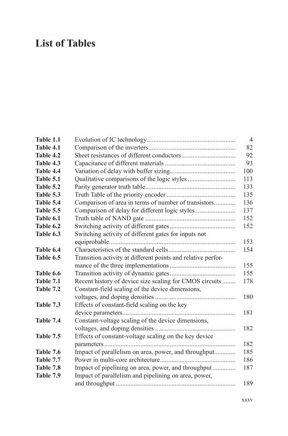
xxxv
List of Tables
Table 1.1 Evolution of IC technology ...................................................... 4Table 4.1 Comparison of the inverters ..................................................... 82Table 4.2 Sheet resistances of different conductors ................................. 92Table 4.3 Capacitance of different materials ........................................... 93Table 4.4 Variation of delay with buffer sizing........................................ 100Table 5.1 Qualitative comparisons of the logic styles ............................. 113Table 5.2 Parity generator truth table ....................................................... 133Table 5.3 Truth Table of the priority encoder .......................................... 135Table 5.4 Comparison of area in terms of number of transistors ............. 136Table 5.5 Comparison of delay for different logic styles......................... 137Table 6.1 Truth table of NAND gate ....................................................... 152Table 6.2 Switching activity of different gates ........................................ 152Table 6.3 Switching activity of different gates for inputs not
equiprobable ............................................................................. 153Table 6.4 Characteristics of the standard cells ......................................... 154Table 6.5 Transition activity at different points and relative perfor-
mance of the three implementations ........................................ 155Table 6.6 Transition activity of dynamic gates ........................................ 155Table 7.1 Recent history of device size scaling for CMOS circuits ........ 178Table 7.2 Constant-field scaling of the device dimensions,
voltages, and doping densities ................................................. 180Table 7.3 Effects of constant-field scaling on the key
device parameters ..................................................................... 181Table 7.4 Constant-voltage scaling of the device dimensions,
voltages, and doping densities ................................................. 182Table 7.5 Effects of constant-voltage scaling on the key device
parameters ................................................................................ 182Table 7.6 Impact of parallelism on area, power, and throughput............. 185Table 7.7 Power in multi-core architecture .............................................. 186Table 7.8 Impact of pipelining on area, power, and throughput .............. 187Table 7.9 Impact of parallelism and pipelining on area, power,
and throughput ......................................................................... 189

xxxvi List of Tables
Table 7.10 Relationship between voltage, frequency, and power .............. 202Table 8.1 Comparison of the die sizes ..................................................... 217Table 8.2 Binary and Gray codes for different decimal values................ 222Table 8.3 Bit transitions per second for different
benchmark programs ................................................................ 223Table 8.4 State assignments using Gray code and binary
code for modulo 6 counter ....................................................... 233Table 8.5 State assignments using Gray code and binary
code for sequence detector ....................................................... 234Table 8.6 Ratio parameter table of f3 ....................................................... 248Table 8.7 Area, delay, and switching power in static
CMOS, dynamic CMOS, and PTL circuits .............................. 252Table 9.1 Input vectors and corresponding leakage currents
for the three-input NAND gate ................................................ 269Table 9.2 Traditional power management states ...................................... 285Table 9.3 Leakage power dissipation in delay-constrained
dual-Vt CMOS circuits ............................................................. 295Table 9.4 Total power dissipation during active mode ............................ 296Table 9.5 Leakage energy dissipation in energy-constrained
dual-Vt CMOS circuits ............................................................. 297Table 9.6 Total energy requirement during active mode ......................... 297Table 9.7 Energy reduction in delay-constrained and energy-con-
strained dual-Vt CMOS circuits ............................................... 298Table 11.1 Measured lifetimes and the delivered charges
for different profiles ................................................................. 339Table 11.2 A table showing the tasks to be scheduled ............................... 343Table 11.3 Energy consumption in three different situations .................... 344Table 11.4 Variation in energy consumption with the change
in duty cycle for 180 nm .......................................................... 344Table 11.5 Variation in energy consumption with the change
in duty cycle for 70 nm ............................................................ 344Table 11.6 States of processor, radio, and the sensor for four
different tasks ........................................................................... 345Table 11.7 Current requirement of different resources used
in realizing the sensor node ...................................................... 345Table 11.8 Energy consumption in three different situations .................... 346Table 11.9 Simulation parameters used in Assisted-LEACH .................... 353Table 11.10 Round versus node death: for the death
of half the network ................................................................... 353Table 11.11 Energy versus round: for intermediate round .......................... 353Table 12.1 Voltage–frequency pairs supported by the
XEEMU simulator ................................................................... 365Table 12.2 Loop unrolling experimental results ........................................ 366Table 12.3 Loop tiling experimental results .............................................. 367Table 12.4 Loop permutation experimental results ................................... 368
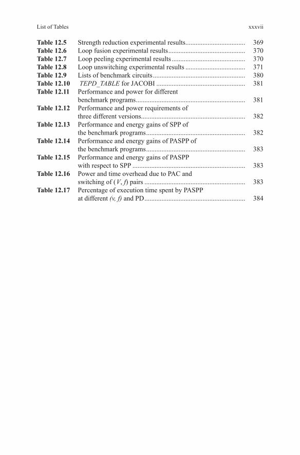
xxxviiList of Tables
Table 12.5 Strength reduction experimental results ................................... 369Table 12.6 Loop fusion experimental results ............................................. 370Table 12.7 Loop peeling experimental results ........................................... 370Table 12.8 Loop unswitching experimental results ................................... 371Table 12.9 Lists of benchmark circuits ...................................................... 380Table 12.10 TEPD_TABLE for JACOBI .................................................... 381Table 12.11 Performance and power for different
benchmark programs ................................................................ 381Table 12.12 Performance and power requirements of
three different versions............................................................. 382Table 12.13 Performance and energy gains of SPP of
the benchmark programs .......................................................... 382Table 12.14 Performance and energy gains of PASPP of
the benchmark programs .......................................................... 383Table 12.15 Performance and energy gains of PASPP
with respect to SPP .................................................................. 383Table 12.16 Power and time overhead due to PAC and
switching of ( V, f) pairs ........................................................... 383Table 12.17 Percentage of execution time spent by PASPP
at different (v, f) and PD ........................................................... 384