Low-power Temperature Sensing System for Biomedical ...
106
Low-power Temperature Sensing System for Biomedical Applications by Hasan Afkhami Ardakani B. Sc., Isfahan University of Technology, 2014 A THESIS SUBMITTED IN PARTIAL FULFILLMENT OF THE REQUIREMENTS FOR THE DEGREE OF MASTER OF APPLIED SCIENCE in THE FACULTY OF GRADUATE AND POSTDOCTORAL STUDIES (ELECTRICAL AND COMPUTER ENGINEERING) THE UNIVERSITY OF BRITISH COLUMBIA (Vancouver) August 2017 © Hasan Afkhami Ardakani, 2017
Transcript of Low-power Temperature Sensing System for Biomedical ...
Low-power Temperature Sensing System for
Biomedical Applications
by
Hasan Afkhami Ardakani
B. Sc., Isfahan University of Technology, 2014
A THESIS SUBMITTED IN PARTIAL FULFILLMENT OF
THE REQUIREMENTS FOR THE DEGREE OF
MASTER OF APPLIED SCIENCE
in
THE FACULTY OF GRADUATE AND POSTDOCTORAL STUDIES
(ELECTRICAL AND COMPUTER ENGINEERING)
THE UNIVERSITY OF BRITISH COLUMBIA
(Vancouver)
August 2017
© Hasan Afkhami Ardakani, 2017

ii
Abstract
Implantable sensors have been used to improve monitoring and diagnosis of health-related
parameters while allowing patients to lead a relatively normal life. Using data from such sensors,
one can detect abnormal conditions at early stages and facilitate the prevention of potentially
serious consequences. Recent technological advances in integrated circuits, wireless
communications, and physiological sensing allow miniature, lightweight, ultra-low-power,
intelligent monitoring devices.
In this thesis, we focus on an electro-thermally active stent technology for management of in-stent
restenosis (i.e., re-narrowing of artery at the stented site). Various studies reporting hyperthermia
treatments of restenosis through stent heating have shown promising results, i.e., moderate local
heating prevents restenosis by limiting cell proliferation. To remotely warm up the stent, we intend
to harvest power from a dedicated source outside of the patient’s body and convert it to heat.
However, if there is no control over temperature, the stent temperature may increase unboundedly,
which would have adverse effects.
The main objective of this thesis is to design a low-power, accurate temperature sensing system
with a small footprint. Further, the required power to operate the temperature sensor should be
harvested. In this work, two different temperature telemonitoring systems have been designed and
laid out in a 65-nm CMOS technology. Both systems have been fabricated and successfully
validated.

iii
The first telemonitoring system converts the sensed temperature directly to a frequency in an
unlicensed band and transmits it to an external reader. The system operates from a supply voltage
of 0.7 𝑉 and a power consumption of 100 µ𝑊. The measured sensitivity of the system is
1.1 𝑀𝐻𝑧/°𝐶 within the frequency band of 902 to 928 MHz. This system is capable of detecting
temperature change to as low as 1 °𝐶.
The sensor interface circuit of our second telemonitoring system converts the temperature to duty-
cycle and sends sensory data out using an on-off-keying modulation system. The pulse width of
the transmitted signal is proportional to e temperature. Measurement results of a proof-of-concept
prototype show that the system operates from a supply voltage of as low as 0.6 𝑉 while
consuming 115 µ𝑊.

iv
Lay Summary
The primary objective of this research is to design a low-power temperature sensing system for
biomedical implants. In particular, the focus of our work is on a smart stent, which is a tube-like
device implanted in the blocked or narrowed artery to keep the lumen open. The stent is wirelessly
heated and uses a temperature sensor for controlling its temperature. The required power for the
temperature sensor operation is harvested from outside of the patient’s body. Two approaches for
transferring the sensor information (temperature) from the implanted device to outside of the
patient’s body are investigated. We have designed and implemented the proposed integrated
temperature sensing system using complementary metal-oxide-semiconductor (CMOS)
technology and have experimentally validated the performance of the system.

v
Preface
This thesis is submitted for the degree of Master of Applied Science at the University of British
Columbia. The research described herein was conducted under the supervision of Professor
Shahriar Mirabbasi, in the Department of Electrical and Computer Engineering, the University of
British Columbia, between September 2015 and August 2017.
Professor Sudip Shekhar provided technical and editing assistance for Chapter 4. In addition, Amir
Masnadi Shirazi provided technical assistance in the design and measurements of the low power
voltage-controlled oscillator (VCO) that is presented in Chapter 4. This work, to the best of my
knowledge, is original, except for where references are made to previous works.
Part of this work has been presented in the following publication:
H. Afkhami, A. Masnadi Shirazi, S. Shekhar, S. Mirabbasi, “A Low Power Temperature Sensing
System for Implantable Biomedical Applications, ” in 2017 IEEE International New Circuits and
Systems Conference (NEWCAS), 2017, pp. 1–4 (Chapter 4).

vi
Table of Contents
Abstract .......................................................................................................................................... ii
Lay Summary ............................................................................................................................... iv
Preface .............................................................................................................................................v
Table of Contents ......................................................................................................................... vi
List of Tables ................................................................................................................................ ix
List of Figures .................................................................................................................................x
List of Abbreviation ................................................................................................................... xiii
Acknowledgements .................................................................................................................... xiv
Dedication .....................................................................................................................................xv
Chapter 1: Introduction to Implantable Biomedical devices .....................................................1
1.1 System Overview ............................................................................................................ 2
1.1.1 General Requirements ................................................................................................. 2
1.2 Wireless Communication Technologies for Implanted Devices .................................... 4
1.2.1 Modulation Methods ................................................................................................... 5
1.2.1.1 AM and ASK Modulation−Demodulation ......................................................... 6
1.2.1.2 FM and FSK Modulation − Demodulation ......................................................... 7
1.2.1.3 PSK Modulation and Demodulation ................................................................... 8
1.2.1.4 Pulse Modulation Encoding ................................................................................ 9
1.3 Conclusion .................................................................................................................... 11
Chapter 2: Temperature effects on Silicon Devices ..................................................................13
2.1 Inductors ....................................................................................................................... 13

vii
2.1.1 Parasitic Resistance ................................................................................................... 15
2.1.2 Parasitic Capacitances ............................................................................................... 17
2.2 Capacitors ..................................................................................................................... 22
2.2.1 Varactors ................................................................................................................... 22
2.3 Inductor Models with Temperature Effect .................................................................... 23
2.4 Temperature Effects on Silicon .................................................................................... 26
2.4.1 Threshold Voltage ..................................................................................................... 27
2.4.2 Mobility..................................................................................................................... 28
2.4.3 Leakage Currents ...................................................................................................... 29
2.4.4 Electrical Conductivity ............................................................................................. 30
2.5 MOSFET Temperature Dependences ........................................................................... 31
2.5.1 On-resistance of MOSFET ....................................................................................... 32
2.5.2 Transconductance (gm) of a MOSFET ...................................................................... 33
2.5.3 Parasitic Capacitances ............................................................................................... 33
2.6 Zero Temperature Coefficient ....................................................................................... 34
2.7 Conclusion .................................................................................................................... 38
Chapter 3: Low-Power VCO for Biomedical Application .......................................................39
3.1 RLC Circuit ................................................................................................................... 39
3.2 Temperature Effects on LC-VCO ................................................................................. 42
3.3 Low Power VCO/Buffer for Biomedical Application .................................................. 48
3.4 Conclusion .................................................................................................................... 54
Chapter 4: A Low-Power Temperature Sensing System for Implantable Biomedical
Applications ..................................................................................................................................55
viii
4.1 Introduction ................................................................................................................... 55
4.2 Temperature Sensor Architecture ................................................................................. 57
4.3 Low-Power FM Transmitter ......................................................................................... 61
4.4 Measurement Results .................................................................................................... 64
4.5 Conclusion .................................................................................................................... 64
Chapter 5: Conclusion .................................................................................................................67
5.1 Future Works ................................................................................................................ 68
Bibliography .................................................................................................................................70
Appendices ....................................................................................................................................78
Appendix A BJT based Temperature Sensor ............................................................................ 78
A.1 CMOS-compatible temperature sensors ................................................................... 79
A.2 BJT based temperature sensors ................................................................................. 82
A.3 Duty cycle modulation and sigma delta ADC .......................................................... 84
Appendix B Two-Stage Folded Cascode OTA ......................................................................... 91

ix
List of Tables
Table 2-1 Conductivity and temperature coefficient of various materials at 20 °C [61]. ............. 31
Table 3-1 Performance comparison of OOK transmitter. ............................................................. 52
Table 4-1 Temperature sensor performance summary and comparison. ...................................... 61
Table 4-2 Performance summary and comparison. ...................................................................... 65
Table 5-1 Performance summary of the proposed systems. ......................................................... 68

x
List of Figures
Figure 1-1 A summary of the potential power sources and the total power from various body-
centered actions [7]. ........................................................................................................................ 3
Figure 1-2 Classification of the communication links based on the physical connection between
TX and RX [3]. ............................................................................................................................... 5
Figure 1-3 AM modulation. ............................................................................................................ 7
Figure 1-4 Principle of ASK modulation. ....................................................................................... 7
Figure 1-5. FM modulation. ............................................................................................................ 8
Figure 1-6 Principle of FSK modulation. ....................................................................................... 8
Figure 1-7 PSK techniques often applied in biotelemetry. ............................................................. 9
Figure 1-8 Constellation diagrams of FSK, ASK, and PSK. .......................................................... 9
Figure 1-9 Pulse modulation encoding techniques. ...................................................................... 10
Figure 2-1 Planar spiral inductors. ................................................................................................ 14
Figure 2-2 Lumped model including magnetic coupling between the spiral and the substrate. ... 15
Figure 2-3 Current distribution in a conductor. ............................................................................ 17
Figure 2-4 Compact frequency-independent inductor model. ...................................................... 18
Figure 2-5 Patterned ground shield (PGS). ................................................................................... 19
Figure 2-6 Lumped one-port inductor model (left) and its equivalent (right). ............................. 20
Figure 2-7 Inductor model at different frequencies and corresponding Q behavior. .................... 21
Figure 2-8 CV characteristic of a MOS varactor, its Q variation and Lumped model. ................ 23
Figure 2-9 Normalized substrate resistance vs. temperature. ....................................................... 25
Figure 2-10 Quality factor vs. frequency. ..................................................................................... 25

xi
Figure 2-11 Change in the threshold voltages of N-channel and P-channel MOSFETS vs.
temperature. .................................................................................................................................. 28
Figure 2-12 Simulation results of IDS –– VGS characteristic at VDS = 0.6 V and at various
temperatures (in TSMC 65nm). .................................................................................................... 35
Figure 2-13 Simulation results of gm –– VGS characteristics at VDS=0.6 V and at various
temperatures (in TSMC 65nm). .................................................................................................... 37
Figure 3-1 Ideal LC circuit (left), Capacitor energy in an ideal LC circuit (center), Pole locations
of an LC circuit in the s-plane (right). .......................................................................................... 40
Figure 3-2 Lossy LC circuit (left), Capacitor energy in lossy LC circuit (center), Pole locations
of an RLC circuit in the s-plane (right). ........................................................................................ 40
Figure 3-3 Linear LC oscillator. ................................................................................................... 41
Figure 3-4 System pole locations on the pole-zero plot and impulse response of the linear LC
oscillator. ....................................................................................................................................... 42
Figure 3-5 Negative feedback system. .......................................................................................... 42
Figure 3-6 A simplified model of LC-tank. .................................................................................. 43
Figure 3-7 Simulation results of a VCO frequency vs. Temperature (a) large inductor (after
compensation) (b) small inductor. ................................................................................................ 47
Figure 3-8 Proposed LC-oscillator/buffer schematic. ................................................................... 49
Figure 3-9 Die photo of the proposed VCO/buffer. ...................................................................... 52
Figure 3-10 Simulation results of the proposed PWM-OOK TX. ................................................ 53
Figure 3-11 Measurement results of the proposed PWM-OOK TX. ............................................ 53
Figure 4-1 A temperature sensor and transmitter for smart-stent implants. ................................. 57
Figure 4-2 Proposed low-power CMOS-based temperature sensor. ............................................ 58

xii
Figure 4-3 Output current versus temperature for the proposed sensor........................................ 59
Figure 4-4 Proposed FM transmitter. ............................................................................................ 62
Figure 4-5 Chip micrograph. ......................................................................................................... 64
Figure 4-6 Measured TCO frequency versus temperature. ........................................................... 65
Figure 4-7 Measured TX output at 914.4 MHz (top) and 926.5 MHz (bottom). .......................... 66
Figure A-1 Structure of a basic electro thermal filter. .................................................................. 80
Figure A-2 CMOS temperature sensor based on temperature-dependent delays of CMOS
inverters......................................................................................................................................... 80
Figure A-3 Cross-section of (a) Lateral PNP BJT; (b) Vertical PNP BJT; and (c) Vertical NPN
BJT. ............................................................................................................................................... 83
Figure A-4 Basic principle of a BJT-based temperature sensor (a) Block diagram of a bandgap
temperature sensor (b) Biasing a BJT pair in a current ratio of p, the single-ended voltages are
CTAT while the differential voltage is PTAT. ............................................................................. 84
Figure A-5 Principle of duty-cycle modulation. ........................................................................... 85
Figure A-6 Principle of sigma-delta ADC. ................................................................................... 85
Figure 5-7 Kelvin-to-Celsius converter implementation. ............................................................. 86
Figure A-8 Detailed circuit diagram of the temperature sensor. .................................................. 88
Figure A-9 Two-stage folded cascode opamp. ............................................................................. 88
Figure A-10 Die photo of the temperature sensor ........................................................................ 89
Figure A-11 Simulation results (Duty Cycle vs. Temperature) .................................................... 90
Figure B-1 Small signal model for two stage folded cascode OTA. ............................................ 91
xiii
List of Abbreviations
ADC Analog-to-digital converter
BJT Bipolar junction transistor
CMOS Complementary metal-oxide-semiconductor
CTAT Complementary to absolute temperature
ISM band Industrial, scientific, and medical radio band
MOSFET Metal–oxide–semiconductor field-effect transistor
OOK On-off keying
OTA Preoperational transconductance amplifier
PTAT Proportional to absolute temperature
PSG Patterned-ground-shield
PWM Pulse width modulation
RF Radio frequency
ST Schmitt trigger
𝑉𝑇ℎ Threshold voltage
𝑔𝑚 Transconductance
VCO Voltage-controlled-oscillator
ZTC Zero temperature coefficient

xiv
Acknowledgements
First and foremost, I wish to express my special gratitude to my supervisor, Professor Shahriar
Mirabbasi, for providing me with direction and technical support. I appreciate his countless advice
on both research as well as on my career. I am grateful for his inspiration, encouragement and
continuous support, throughout my master studies. I would also like to thank Dr. Sudip Shekhar
for his scientific advice and insightful suggestions.
I would like to thank the members of the SoC group with whom I had the opportunity to work.
They provided a friendly and cooperative atmosphere in our research group and offered useful
feedback and insightful comments on my work.
I would like to thank Dr. Roberto Rosales for his technical assistance, and Roozbeh Mehrabadi for
computer-aided design (CAD) tools support. I would also like to thank Canadian Microelectronics
Corporation (CMC Microsystems) for providing CAD tools support and facilitating chip
fabrication.
I would also like to acknowledge the Natural Sciences and Engineering Research Council of
Canada (NSERC) and the Canadian Institutes of Health Research (CIHR) for funding this project.
My sincere thanks goes out to all of my friends and family who supported me in my journey and
incentivized me to strive to achieve my goals. Special thanks are owed to my parents, whose love
and guidance are with me in whatever I pursue. I appreciate their endless support and
encouragement. Dedication

xv
Dedication
To my parents

1
Chapter 1: Introduction to Implantable Biomedical devices
Recent technological advances in integrated circuits and wireless communication have changed
the concept of healthcare, and have revolutionized the realization of biomedical devices for health
monitoring, diagnosis, and wireless telemetry sensors. Significant progress has been made in the
development and improvement of implantable devices (IDs), despite numerous challenges such as
power consumption and power delivery [1]. These devices aim to provide patient safety and
comfort, and to minimize the cost and risk associated with repeated and invasive surgical
procedures [2].
Implantable devices may be powered by batteries or wireless telemetry. Rechargeable and battery-
less implantable devices are preferred, as batteries can contribute to the overall size and weight of
the device. In addition, non-rechargeable batteries must be surgically replaced. These implantable
devices usually communicate with a connection outside of the body through inductive coupling
links. Given the available power to the implantable device, choosing the proper modulation and
data transmission methods can assist in the further reduction of power consumption and can
facilitate secure and fast data transmission. We note that implantable devices should also be
biocompatible to prevent any toxic reactions or infections. In addition, longevity and reliability of
implantable devices are essential given the cost and time associated with surgical implantation
procedures and the patient's recovery [3].
In general, the design of implantable sensors and the corresponding wireless telemetry system is
driven by achieving simplicity, a small footprint, low weight, low power operation and efficient
transceiver architecture.

2
In this chapter, a discussion on the challenges of designing implantable devices and a brief
overview of the possible solutions to these challenges are presented. We discuss analog and digital
modulation techniques that can potentially be used for implantable devices.
1.1 System Overview
Implantable systems and wireless telemetry devices generally comprise of two fundamental
components; an external part located outside of the host body and an internal (implanted) part. The
internal component detects, collects and transfers the information to the external receiver via a
wireless link (typically an inductive coupling link). The external component is usually used to
supply power for the internal component, and/or to analyze and transmit the data to the internal
component [2], [4]. In this research project, we focus on the internal (implantable) block.
1.1.1 General Requirements
When designing a biomedical implantable device, several requirements should be considered.
They are listed as follows:
• Low Power Consumption: Power consumption is the main requirement for IDs, as
extensive dissipation can drain batteries quickly and may damage soft tissues. IDs can be
powered using batteries or wireless power transfer. However, replacement of batteries may
require several costly and invasive surgeries. On the other hand, frequent recharging is
inconvenient and time-consuming [2]. Wireless power can provide continuous power as an
alternative, although the low power restriction should also be applied to ensure that IEEE
human tissue exposure standards are met [5]. More recently, much research has been
3
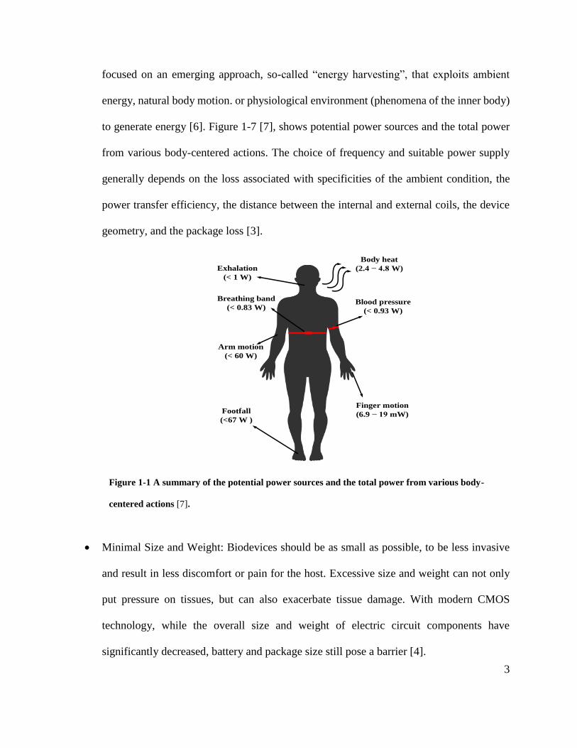
focused on an emerging approach, so-called “energy harvesting”, that exploits ambient
energy, natural body motion. or physiological environment (phenomena of the inner body)
to generate energy [6]. Figure 1-7 [7], shows potential power sources and the total power
from various body-centered actions. The choice of frequency and suitable power supply
generally depends on the loss associated with specificities of the ambient condition, the
power transfer efficiency, the distance between the internal and external coils, the device
geometry, and the package loss [3].
• Minimal Size and Weight: Biodevices should be as small as possible, to be less invasive
and result in less discomfort or pain for the host. Excessive size and weight can not only
put pressure on tissues, but can also exacerbate tissue damage. With modern CMOS
technology, while the overall size and weight of electric circuit components have
significantly decreased, battery and package size still pose a barrier [4].
`
Body heat
(2.4 W)Exhalation
(< 1 W)
Breathing band
(< 0.83 W)Blood pressure
(< 0.93 W)
Arm motion
(< 60 W)
Finger motion
(6.9 mW)Footfall
(<67 W )
Figure 1-1 A summary of the potential power sources and the total power from various body-
centered actions [7].

4
• Biocompatibility: In general, integrity and reliability of IDs can be provided by proper
packaging within all unexpected and hostile environments inside the human body. Proper
packaging can also protect host tissues from potentially harmful elements of the device,
and can offer mechanical support for the implantable device [3], [4].
• Low Voltage Signal and Low Frequencies: Natural signals inside the human body are in
the mV or µV range. Hence, low noise systems should be designed to detect small
biological signals with minimal power consumption and size. The frequency span of
biological signals is between the range of a few hertz to a few kilohertz. In addition, the
medical implant communication system (MICS) and the industrial, scientific, and medical
radio (ISM) band frequencies have been specifically designated for in vivo and in vitro
medical devices [2]. Low voltage and frequency signals demand special care during
sensing, amplifying, modulating and transferring.
• High Reliability: A failure in biomedical devices can result in pain, damage or even death
for the patient. Device maintenance is also complicated and costly, and risks the health of
the patient [2]. Therefore, long-term implantable devices with high reliability are essential.
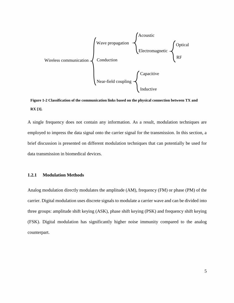
1.2 Wireless Communication Technologies for Implanted Devices
Wireless communication between the implanted device (internal) and the external component can
be divided into three classes: wave propagation, electrical conduction, and near-field coupling, as
shown in Figure 1-2. In this project, only radio-frequency wireless communication is used for data
transmission. Further discussion on wireless communication is beyond the scope of this research
project and can be found in [3].
5
A single frequency does not contain any information. As a result, modulation techniques are
employed to impress the data signal onto the carrier signal for the transmission. In this section, a
brief discussion is presented on different modulation techniques that can potentially be used for
data transmission in biomedical devices.
1.2.1 Modulation Methods
Analog modulation directly modulates the amplitude (AM), frequency (FM) or phase (PM) of the
carrier. Digital modulation uses discrete signals to modulate a carrier wave and can be divided into
three groups: amplitude shift keying (ASK), phase shift keying (PSK) and frequency shift keying
(FSK). Digital modulation has significantly higher noise immunity compared to the analog
counterpart.
Figure 1-2 Classification of the communication links based on the physical connection between TX and
RX [3].
Wireless communication
Wave propagation
Conduction
Near-field coupling
Electromagnetic
Acuostic
Inductive
Capacitive
Optical
RF
Acoustic

6
Modulation techniques can provide a high data rate, security, low power consumption, good
performance, and noise immunity. The proper modulation methods can be selected based on
available power, bandwidth, system efficiency, and considering the channel characteristics.
1.2.1.1 AM and ASK Modulation−Demodulation
In amplitude modulation the amplitude of the carrier is modulated, as depicted in Figure 1-3.
Although an AM based system is the simplest to implement, as the demodulator is only using an
envelope detector, it is rarely used in biomedical devices due to weak noise immunity. The digital
form of AM, so-called ASK, is significantly less sensitive as it has only two possible carrier
amplitudes.
Nowadays, the simplest digital modulation used in biomedical devices is ASK or on-off keying
(OOK). Figure 1-4 shows the principle of ASK modulation. ASK is the most commonly used
modulation technique for wireless telemetry devices because of its simplicity and low power
consumption. Several ASK demodulators have been proposed and developed; however, they suffer
from high power consumption and/or large area overhead. In general, ASK demodulators used in
biomedical applications consist of an envelope detector, digital shaper, and load driver.
ASK modulation is also widely used for inductive power transfer, as the tuned coupled coils can
operate in the most efficient way if they work continuously. Further, ASK modulation has strong
noise performance as its input is pulse modulated (only zero or one) [3].

7
1.2.1.2 FM and FSK Modulation − Demodulation
In frequency modulation, phase or frequency of the carrier is modulated with the source signal. In
analog modulation, it is difficult to distinguish frequency modulation from phase modulation. In
this modulation, a voltage controlled oscillator (VCO) generates a carrier and its frequency
depends on the control voltage (source signal). Since the information contains frequency, FM is
not as sensitive to amplitude noise. A phase locked-loop (PLL) can also be used to generate
modulated frequencies; however, because of power consumption, PLL is not usually
recommended for implanted devices. For instance, the center frequency can vary from a few
kilohertz to a few gigahertz. Alternatively, much research has been focused on MICS band
designated for biomedical devices. More details of a practical circuit for frequency modulation are
discussed in chapter 4.
Time
Amplitude Amplitude
Time
Baseband signal
AM
Figure 1-3 AM modulation.
1 0 1 1 0 1 1 1
Data (Baseband) ASK Signal
Time
Amplitude
Time
Amplitude0 0
Figure 1-4 Principle of ASK modulation.

8
FSK is one of the earliest digital modulation techniques used for biomedical applications. The
principle of FSK modulation is shown in Figure 1-6. In this method, a digital source modulates a
VCO input by changing the varactor between two values.
1.2.1.3 PSK Modulation and Demodulation
In the last few decades, much research has been focused on PSK modulation for low power
applications. In this modulation, the carrier phase is modulated by 180 degrees (depicted in Figure
1-7) which can be implemented by using an active/passive mixer or balun transformer. The
detected signal is compared with a reference signal generated by the carrier recovery circuit that
is synchronous to the received signal. In biomedical devices, the absolute received phase is not
known and therefore differential PSK (DPSK) is commonly used [3].
As noted previously, when comparing FSK and ASK the former is less sensitive to amplitude
noise. PSK has also been proven superior to FSK concerning noise immunity. To clarify, phase is
Baseband signal
Time
AmplitudeFM
Time
Amplitude
Figure 1-5. FM modulation.
1 0 1 1 0 1 1 1
Data (Baseband) ASK Signal
Time
Amplitude
Time
Amplitude0 0
Figure 1-6 Principle of FSK modulation.

9
the time integral of frequency, and it can be interpreted that PSK averages out noise over the
bandwidth of interest. Figure 1-8 shows the constellation diagram of ASK, PSK and FSK, from
which the concept of noise immunity can be comprehended.
1.2.1.4 Pulse Modulation Encoding
Thus far, pure analog and pure digital modulation have been discussed, which exhibit several
drawbacks such as: complex demodulators, large appetite for power, and sensitivity to noise, to
name a few. Pulse modulation is an alternative approach, which combines both pure modulations
to achieve better signal to noise ratio at the cost of larger bandwidth occupation [2].
1 0 1 1 0 1 1 1
Data (Baseband) ASK Signal
Time
Amplitude
Time
Amplitude0 0
Figure 1-7 PSK techniques often applied in biotelemetry.
Q
I
Q
I
'0' '1'
Q
I
'0' '1''0' '1'
Figure 1-8 Constellation diagrams of FSK, ASK, and PSK.

10
In this modulation, the pulse modulated signal remains analog, but the transmission takes place at
discrete times. Analog pulse modulation can be classified into four groups: pulse-amplitude
(PAM), pulse-width (PWM) or pulse duration (PDM), pulse-position (PPM) or pulse interval
modulation (PIM), and pulse-frequency modulation (PFM). For digital pulse modulation, called
pulse-code-modulation (PCM), the analog signal is first quantized and then converted to a pulse
train [3].
When a signal is sampled and held for a constant time, PAM can be achieved. Nonetheless, holding
the signal value limits PAM’s required bandwidth, causing signal distortion and increasing the
reception circuitry’s complexity. PWM is usually achieved by comparing the original signal with
a sawtooth waveform, where the duty cycle of the PWM signal is proportional to the sampled
value. A 15-channel neural recording interface using PWM time division multiplexed FM, and a
15-channel PDM-FM modulated telemeter for biomedical monitoring, were described in [8] and
[9], respectively. For PPM and PIM, a PWM signal should be generated first, followed by the
transmission of falling edges (PPM) or both edges (PPM). A blood pressure sensor, bladder
pressure telemetry system [10], and eye pressure sensor [11] were described using PPM and PIM
modulation, respectively.
Baseband
signal
Time
Amplitude PAM
Time
Amplitude PWM/PDM
Time
Amplitude PPM/PIM
Time
Amplitude PFM
Figure 1-9 Pulse modulation encoding techniques.

11
1.3 Conclusion
In general, most biomedical devices have similar agreed-upon requirements, such as exhibiting
low power consumption, a small footprint, biocompatibility, and high reliability. To minimize
invasive effects of bio-devices, the devices themselves need to be as small as possible. Researchers
have been working on various solutions to meet these requirements, such as power harvesting and
inductive coupling with the aim of eliminating batteries from implanted devices. This direction
has been chosen due to the relevant problems associated with batteries in implanted devices, such
as limited lifetime, large size, and chemical side effects. Addressing this, a package and
encapsulation layer can protect the implanted device under the body’s harsh environment.
Furthermore, upholding biocompatibility ensures that host organs, such as tissues, vessels, etc.,
will not react to the aforementioned potentially harmful elements of the device. In addition to the
safety and comfort of the patient, the economy of an implantable device is also important,
especially with the increased use of these devices.
In this chapter, different modulation techniques suitable for an implantable device’s data
communication have been discussed. The proper modulation is selected based on the available
power, the distance between transmitter and receiver, and the nature and type of the implanted
device. We see that digital modulations are less sensitive to noise compared to analog modulations.
FSK modulation can also offer a high data rate; however, it suffers from complicated
transceivers/receivers and size issues. The ASK modulation is utilized predominantly for short-
range communication because of noise sensitivity issues, while PSK can be used for long distance
transmission owing to its superior noise performance. However, PSK may not be suitable for high
data rate applications due to bandwidth limitations and demodulator power consumption.

12
Carrier frequency is also very important as it can alter power consumption and size. In general, the
human body can safely be exposed to RF electromagnetic fields between 3 kHz – 30 GHz. The
Medical Implant Communication System (MICS) band and the second ISM (Industrial, Scientific,
and Medical) band are specified between the frequencies of 402–405 MHz and 902–928 MHz,
respectively, and are commonly used for biomedical devices.
13
Chapter 2: Temperature effects on Silicon Devices
A major success of today’s integrated circuits has been the ability to incorporate numerous on-
chip elements, such as resistors, capacitors, and more importantly, inductors, with active devices.
In this chapter, on-chip inductors and capacitors used in analog design are discussed. A brief
discussion of the physical models of passive components is also presented, in addition to a more
detailed study of the temperature-related aspect of integrated circuits. We conclude this chapter by
presenting the principles and design tradeoffs of circuits less sensitive to temperature based on the
zero-temperature coefficient point.
2.1 Inductors
Circular spiral integrated inductors show relatively good performance among chip inductors, but
due to fabrication limitations, hexagonal and octagonal structures are typically used. The topmost
metal layer, which incorporates the thickest available metal, is usually employed to minimize
losses and to achieve a better quality factor (Q). In this section, a brief discussion on inductor
models is provided. We begin with the self-inductance of multi-turn spiral inductors [12],
𝐿 ≈
𝜇
2𝜋
𝑙53
[𝑙4𝑁 +𝑊 + (𝑁 − 1)(𝑊 + 𝑆)]
13 𝑊0.083 (𝑊 + 𝑆)0.25
(2.1)
where 𝑁 is the umber of turns and 𝑆 is the spacing between two adjacent legs (all units are metric).

14
The quality factor is defined as energy stored in a capacitor or inductor to the average power loss
for a sinusoidal excitation,
𝑄 = 𝜔𝑒𝑛𝑒𝑟𝑔𝑦 𝑠𝑡𝑜𝑟𝑒𝑑
𝑎𝑣𝑒𝑟𝑎𝑔𝑒 𝑝𝑜𝑤𝑒𝑟 𝑙𝑜𝑠𝑠= 2𝜋
𝑒𝑛𝑒𝑟𝑔𝑦 𝑠𝑡𝑜𝑟𝑒𝑑
𝑒𝑛𝑒𝑟𝑔𝑦 𝑙𝑜𝑠𝑡 𝑝𝑒𝑟 𝑐𝑦𝑐𝑙𝑒 (2.2)
Since only resistive components dissipate power, various resistances within or around the inductor
should be studied. These loss mechanism studies lead us to develop a model for integrated
inductors.
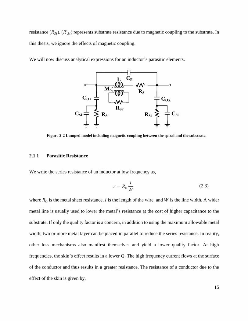
An equivalent circuit model for inductors can aid designers in developing a simple RLC circuit
that can be used in the simulation. Here, lumped Π models for spiral inductors are commonly used,
which represent the physical mechanisms taking place in the inductor. In addition, the
approximation from this method is valid over a wide range of frequencies. Figure 2-2 reviews the
single Π structure. This model consists of low-frequency series inductance (𝐿), the series ohmic
resistance (𝑅𝑆), the feedforward capacitance (𝐶𝐹) which models the capacitance between metal
lines, the oxide to substrate capacitance (𝐶𝑂𝑋), the substrate capacitance (𝐶𝑆𝑖), and substrate
Dout
S
Din
W
Figure 2-1 Planar spiral inductors.
15
resistance (𝑅𝑆𝑖). (𝑅′𝑆𝑖) represents substrate resistance due to magnetic coupling to the substrate. In
this thesis, we ignore the effects of magnetic coupling.
We will now discuss analytical expressions for an inductor’s parasitic elements.
2.1.1 Parasitic Resistance
We write the series resistance of an inductor at low frequency as,
𝑟 = 𝑅𝑙
𝑊 (2.3)
where 𝑅 is the metal sheet resistance, 𝑙 is the length of the wire, and 𝑊 is the line width. A wider
metal line is usually used to lower the metal’s resistance at the cost of higher capacitance to the
substrate. If only the quality factor is a concern, in addition to using the maximum allowable metal
width, two or more metal layer can be placed in parallel to reduce the series resistance. In reality,
other loss mechanisms also manifest themselves and yield a lower quality factor. At high
frequencies, the skin’s effect results in a lower Q. The high frequency current flows at the surface
of the conductor and thus results in a greater resistance. The resistance of a conductor due to the
effect of the skin is given by,
L
RS
COX COX
CSiCSi RSiRSi
CF
M
RSi'
Figure 2-2 Lumped model including magnetic coupling between the spiral and the substrate.

16
𝑅𝑠𝑘𝑖𝑛 =1
𝛿𝜎 (2.4)
where 𝜎 denotes conductivity and 𝛿 is the skin depth. Skin depth is given by,
𝛿 =1
√𝜋𝑓µ𝜎 (≈ 2.5 𝜇𝑚 𝑎𝑡 1 𝐺𝐻𝑧) (2.5)
where 𝑓 is the frequency and µ is the permeability. Therefore, as a first order approximation, the
series resistance expression can be modified to include the skin effect as,
𝑅𝑆 = 𝑟𝑡
𝛿 (1 − 𝑒−𝑡𝛿) (2.6)
where 𝑡 is the metal thickness.
Eddy current produced by the magnetic field of the adjacent turns also alters the current
concentration in metal, which is the so-called “proximity effect”. Considering the skin and
proximity effect, one can show that the resistance of a multi-turn spiral inductor is highly
frequency-dependent. In practice, the proximity effect can be ignored, as it is not significant
compared to the skin effect. In [13] an analytical equation is derived from fundamental
electromagnetic principles,
𝑅𝑒𝑓𝑓 = 𝑅𝑜 [1 +1
10(𝑓
𝑓𝑐𝑟𝑖𝑡)2
] (2.7)
where 𝑅𝑜 is the DC resistance and 𝑓𝑐𝑟𝑖𝑡 can be calculated from the geometrical size of the inductor.
In this project, because of the limited operational frequency range (902~928 𝑀𝐻𝑧), and a
relatively large 𝑓𝑐𝑟𝑖𝑡 (~1.7 𝐺𝐻𝑧), we can assume that the series resistance is constant and
frequency-independent over the abovementioned frequency range.

17
2.1.2 Parasitic Capacitances
Apart from the ohmic loss described above, parasitic capacitance also limits an inductor’s
performance by limiting the maximum frequency in which the inductor can be used (called the
“self-resonance frequency”). Parallel plate capacitances and fringe capacitances are connected to
the lossy substrate which can degrade the quality factor. Capacitive and magnetic coupling to the
substrate can also create displacement and eddy current in the substrate, respectively, as well as
degrading the quality factor. Both the eddy and displacement currents can be reduced using a
grounded-shield plate, although the effective inductance will fall in this case and yield a low Q.
These effects manifest themselves at a multi Gigahertz regime; however, because of the frequency
operation of our devices, we can ignore these effects and simplify the lumped model shown in
Figure 2-4.
`
`
`
`
DC Condition
Skin Effect
Proximity
Effect
Frequency
Number of parallel lines
Current Density
Figure 2-3 Current distribution in a conductor.

18
𝐶𝐹 represents fringe capacitance and the overlap capacitance between the spiral and the underpass
required to connect the inner end of the spiral inductor to external circuitry. This capacitor can be
approximated by,
𝐶𝐹 ≈𝐴𝑜𝑣𝑡𝑜𝑥𝑎𝑑
휀𝑜𝑥 (2.8)
where 𝐴𝑜𝑣 is the overlap area, 휀𝑜𝑥 is the permittivity of the oxide layer (휀𝑜𝑥 = 3.45 ∗ 10−13𝐹/𝑐𝑚)
between the spiral and the underpass, and 𝑡𝑜𝑥𝑎𝑑 is the oxide thickness between the two metal layers.
Fringe capacitance between two adjacent legs can be neglected due to its usual small size.
𝐶𝑜𝑥 is the capacitance between the spiral and the lossy substrate, which accounts for most of the
inductor’s parasitic capacitance. It is given by,
𝐶𝑜𝑥 =1
2
휀𝑜𝑥𝑑𝑜𝑥
𝑙𝑊 (2.9)
where 𝑑𝑜𝑥 is the distance between the spiral and the substrate. The substrate capacitance and
resistance can be expressed as,
𝐶𝑆𝑖 =1
2 𝐶𝑠𝑢𝑏𝑙𝑊 (2.10)
L
RS
COX COX
CSiCSi RSiRSi
CF
Figure 2-4 Compact frequency-independent inductor model.

19
𝑅𝑆𝑖 =2
𝐺𝑠𝑢𝑏𝑙𝑊 (2.11)
where 𝐶𝑠𝑢𝑏 and 𝐺𝑠𝑢𝑏 are the substrate capacitance and resistance per unit area, respectively. Both
fit the parameters and constants for a given substrate.
We can improve inductor performance using a patterned ground shield (PSG). In this approach, a
poly or metal layer is inserted beneath the spiral inductor and is connected to the ground. The
ground shield reduces the distance between the substrate and spiral metal, and thereby reduces the
effective resistance. The ground shield can then be broken to cut the eddy current loop. In other
words, the ground shield should be patterned so that flux can pass through while grounding the
electric field [14]. Such a PSG is shown in Figure 2-5. A PSG slightly affects inductance and
increases the peak Q; however, it reduces the self-resonant frequency due to increasing parasitic
capacitance since the ground shield is closer to the spiral. In general, in order to minimize PSG
resistance, a metal with lowest resistance and furthest distance away from the substrate should be
used. Parallel metal strips can be used to further reduce the resistance.
Figure 2-5 Patterned ground shield (PGS).

20
To avoid unnecessary complex calculations, we assume a single-ended configuration where one
of the terminals of the inductor is grounded, as shown in Figure 2-6 on the left side, to determine
the quality factor of the inductor. On the right side of Figure 2-6, a simplified model is depicted
where, 𝑅𝑆𝑖, 𝐶𝑆𝑖 and 𝐶𝑜𝑥 are replaced with an equivalent shunt resistance (𝑅𝑃) and capacitance (𝐶𝑃).
𝑅𝑃 and 𝐶𝑃 are expressed by,
𝑅𝑃 =1
𝜔 𝐶𝑜𝑥2 𝑅𝑆𝑖+𝑅𝑆𝑖 (𝐶𝑜𝑥 + 𝐶𝑆𝑖)
2
𝐶𝑜𝑥2 ≈
1
𝜔 𝐶𝑜𝑥2 𝑅𝑆𝑖+ 𝑅𝑆𝑖 ≈ 𝑅𝑆𝑖
(2.12)
𝐶𝑃 = 𝐶𝑜𝑥1 + 𝜔2𝑅𝑆𝑖
2 𝐶𝑆𝑖 (𝐶𝑜𝑥 + 𝐶𝑆𝑖)
1 + 𝜔2𝑅𝑆𝑖2 (𝐶𝑜𝑥 + 𝐶𝑆𝑖)2
≈𝐶𝑜𝑥𝐶𝑆𝑖𝐶𝑜𝑥 + 𝐶𝑆𝑖
= 𝐶𝑜𝑥|| 𝐶𝑆𝑖 (2.13)
𝐿𝑠 does not decrease significantly with increasing frequency because it is predominantly
determined by the magnetic flux external to the conductor [15]. Consequently, it is valid to model
𝐿𝑠 as a constant. Additionally, because of our small bandwidth of interest we can assume that the
inductance is constant.
An ideal inductor is expected to be a pure energy storage element. In reality, however, parasitic
resistances result in power dissipation and parasitic capacitances reduce the inductance. Therefore,
the definition of a quality factor includes a description of how an inductor works as a storage
element [14]. For an inductor, the quality factor is defined as [16],
COX
CSiRSi
LS
RS
CF CPRP
LS
RS
CF
Figure 2-6 Lumped one-port inductor model (left) and its equivalent (right).

21
𝑄 = 2𝜋. (𝑃𝑒𝑎𝑘 𝑀𝑎𝑔𝑛𝑒𝑡𝑖𝑐 𝐸𝑛𝑒𝑟𝑔𝑦 − 𝑃𝑒𝑎𝑘 𝐸𝑙𝑒𝑐𝑡𝑟𝑖𝑐 𝐸𝑛𝑒𝑟𝑔𝑦
𝐸𝑛𝑒𝑟𝑔𝑦 𝐿𝑜𝑠𝑠 𝑖𝑛 𝑂𝑛𝑒 𝑂𝑠𝑐𝑖𝑙𝑙𝑎𝑡𝑖𝑜𝑛 𝐶𝑦𝑐𝑙𝑒) (2.14)
𝑄𝑜𝑛−𝑐ℎ𝑖𝑝
=𝜔𝐿
𝑅𝑠.
𝑅𝑃
𝑅𝑃 + 𝑅𝑆[1 + (𝜔𝐿𝑅𝑆)2
]
. [1 − (𝐶𝐹 + 𝐶𝑃)(𝑅𝑆2
𝐿+ 𝜔2𝐿)]
(2.15)
The first term here represents the series loss in the spiral. The second term accounts for the silicon
substrate loss and the last term is the self-resonant factor representing the reduction in Q due to
the increase in peak electric energy with increasing frequency [16]. The self-resonant frequency
ωOsc is
𝜔𝑂𝑠𝑐 = √1
𝐿(𝐶𝐹 + 𝐶𝑃)[1 −
𝑅𝑆2
𝐿(𝐶𝑃 + 𝐶𝐹)]
(2.16)
Given the foregoing equation, we can sketch an approximation of Q as a function of frequency, as
shown below in Figure 2-7. At low frequencies, the series resistance (𝑟𝑆) defines Q. The quality
factor increases linearly up to a point where the skin effect becomes significant. At high
frequencies, 𝑅𝑆𝑢𝑏 shunts the inductor and limits the Q [16].
SR
L
skinS RR
L
L
Rsub
Q
ω
LRS L RS RSkin
L RS RSkin
RSub
Figure 2-7 Inductor model at different frequencies and corresponding Q behavior.
Substrate Loss
Factor
Self-Resonance Factor
22
2.2 Capacitors
The gate capacitance of MOSFET can be used to realize the nonlinear capacitors with highest
density. MOS capacitors (MOSCAP) may be utilized where linearity and power consumption is
not a concern. We note that channel resistance limits the Q of the capacitors, and gate leakage can
drain the battery. Fringe capacitors may be used if the Q or linearity of MOSCAP is not adequate.
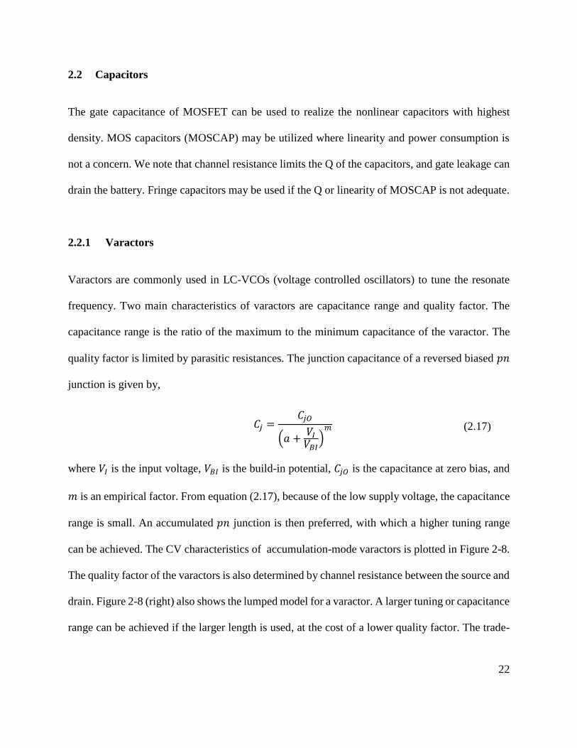
2.2.1 Varactors
Varactors are commonly used in LC-VCOs (voltage controlled oscillators) to tune the resonate
frequency. Two main characteristics of varactors are capacitance range and quality factor. The
capacitance range is the ratio of the maximum to the minimum capacitance of the varactor. The
quality factor is limited by parasitic resistances. The junction capacitance of a reversed biased 𝑝𝑛
junction is given by,
𝐶𝑗 =
𝐶𝑗𝑂
(𝑎 +𝑉𝐼𝑉𝐵𝐼)𝑚 (2.17)
where 𝑉𝐼 is the input voltage, 𝑉𝐵𝐼 is the build-in potential, 𝐶𝑗𝑂 is the capacitance at zero bias, and
𝑚 is an empirical factor. From equation (2.17), because of the low supply voltage, the capacitance
range is small. An accumulated 𝑝𝑛 junction is then preferred, with which a higher tuning range
can be achieved. The CV characteristics of accumulation-mode varactors is plotted in Figure 2-8.
The quality factor of the varactors is also determined by channel resistance between the source and
drain. Figure 2-8 (right) also shows the lumped model for a varactor. A larger tuning or capacitance
range can be achieved if the larger length is used, at the cost of a lower quality factor. The trade-

23
off between the capacitance range and Q of varactors ultimately leads to another trade-off between
the tuning range and phase noise of LC VCOs [12].
2.3 Inductor Models with Temperature Effect
In this section, the temperature dependency of on-chip, planar, spiral inductors is analyzed and
characterized. The temperature dependence of the quality factor can be explained in the context of
the temperature coefficient of the parasitic resistance. The series and shunt resistances exhibit a
strong dependence on temperature and frequency. Throughout this section, we will examine how
temperature affects on-chip inductors. We will then discuss the problem of temperature variation
in inductors and a temperature model for inductors will be presented.
As discussed previously, the inductance of a planar spiral is frequency and geometry-dependent;
however, because of our frequency and the frequency range of interest, we can assume that the
inductance is frequency-independent. The geometry of inductors varies with the number of turns,
line spacing, line width, line thickness, and the outside radius of the inductor. Therefore,
inductance behavior is well understood and is not expected to vary significantly with temperature
VGS
CGS
Cmax
Cmin
VGS
Q
00
Rvar
Cvar
S
G
Figure 2-8 CV characteristic of a MOS varactor, its Q variation and Lumped model.

24
[17]. Our simulation shows that inductance will change approximately 0.013 𝑛𝐻/°𝐶 up to the self-
resonant frequency,
𝐿 = 𝐿𝑂(𝜌𝐿(𝑡𝑒𝑚𝑝𝑟𝑒𝑎𝑡𝑢𝑟𝑒 − 25) + 1) (2.18)
where 𝐿𝑂 is the inductance at 25 °𝐶.
Parasitic resistance, as we have mentioned, defines the quality factor of the inductor. Metal series
resistance is linearly temperature-dependent. Series resistance modeling the effect of skin,
however, has a lower temperature coefficient, yet it is highly frequency-dependent. Our
simulations show that substrate resistance has a positive temperature coefficient for temperatures
below roughly 100 °𝐶, while for temperatures greater than 100 °𝐶 the substrate resistance shows
a negative temperature coefficient. Hence, Q is expected to vary with temperature as parasitic
resistances change. Further, Q decreases with increasing temperature at low frequencies because
of the positive temperature coefficient of series resistances. At high frequencies, the primary power
loss of the inductor is dominated by the substrate resistance (where the overlap capacitances shunt
out the series resistances), and the substrate resistance increases with the temperature increase.
In order to modify the inductor model, we obtained a linear equation for the parasitic resistances
[18]. It should be noted that, although the substrate and skin effect resistances are significantly
frequency-dependent, we assume that they are constant over the bandwidth of interest. The
substrate resistor shows higher order nonlinearity, as shown in Figure 2-9. This is modeled linearly
owing to the limited temperature range.
Metal series resistance is given by,
𝑟(𝑇) ≈ 𝑟𝑜(𝛼. ∆𝑇 + 1) (2.19)
The substrate resistance can be expressed as,

25
𝑅𝑆𝑖 ≈ 𝑅𝑆𝑖𝑜(𝛽1. ∆𝑇2 + 𝛽2. ∆𝑇 + 1) → 𝑅𝑆𝑖𝑜 ≈ 𝑅𝑠𝑢𝑏(𝛽3. ∆𝑇 + 1)
(2.20)
The resistance modelling the metal track’s skin effect is,
𝑅𝑆𝑘𝑖𝑛𝑛(𝑇) ≈ 𝑅𝑆𝑘𝑖𝑛𝑛𝑜 ∗ (𝜂1. ∆𝑇 + 1) (2.21)
Figure 2-9 Normalized substrate resistance vs. temperature.
SR
LskinS RR
L
L
Rsub
Q
ω
LRS
L RS RSkin L RS RSkin
RSub
L
RSub
-0.0034 °C -1
-0.0046 °C -1
-0.001 °C -1
temp < 100 °C
+0.003 °C -1
(temp < 100 °C)
Temperature
Coefficient
Figure 2-10 Quality factor vs. frequency.

26
where ∆𝑇 = 𝑇 − 𝑇𝑛𝑜𝑚𝑖𝑛𝑎𝑙(25 °𝐶), 𝑟𝑜 , 𝑅𝑆𝑖𝑜and 𝑅𝑆𝑘𝑖𝑛𝑛𝑜 are resistance at 25 °𝐶, and 𝛼, 𝛽1, 𝛽2, 𝛽3 and
𝜂1 are the temperature coefficients (𝛼 = 0.0034 °𝐶−1, 𝛽1 = −0.00003 °𝐶−1, 𝛽2 =
0.004 °𝐶−2, 𝛽3 = 0.003 °𝐶−1 and 𝜂1 = 0.0012 °𝐶
−1 ).
Simulation results show that PSG can aid in reducing inductor coupling with the substrate and
thereby decreases the effect of the parasitic substrate. We note that PSG reduces the electric
coupling, while flux still passes through the PSG to the substrate. In other words, at very high
frequencies and high temperature, the substrate’s parasitic resistance affects the quality factor. This
can be explained by the fact that the coupling of the inductor to the substrate (eddy current) is
neglected, as shown in Figure 2-2. The difference in temperature coefficients between metal layers
(inductor layer and the patterned ground shield layer) is overridden by the substrate loss at high
temperature and high frequency, as the Si substrate is more sensitive to temperature [19].
2.4 Temperature Effects on Silicon
A change in temperature can generally affect the MOSFET threshold voltage, leakage current,
mobility, carrier diffusion, interconnect resistance, velocity saturation, energy band gap, current
density, carrier density, and electromigration. In other words, temperature variation can impact the
power, speed, and reliability of a system [20]. We will examine temperature effects on the critical
parameters of MOSFETs, such as threshold voltage, leakage current, mobility, and interconnect
resistance. We will show that MOSFETs can demonstrate a positive, negative, or zero temperature
coefficient. The effects of temperature on the dynamic responses of MOSFETs are also provided.

27
2.4.1 Threshold Voltage
A precise evaluation of temperature dependence of the threshold voltage is important, not only
because of a MOSFET’s voltage-current characteristics (ie., a small change in threshold voltage
causes a large change in the output current), but also because a system should be able to operate
over a wide range of temperatures. Therefore, an accurate model for temperature changes and the
effects of such changes on threshold voltages is required for circuit design. The threshold voltage
of a MOSFET is found to be linearly increased with decreasing temperature. Accordingly, we can
model the threshold voltage by,
𝑉𝑡ℎ(𝑇) = 𝑉𝑡ℎ𝑜 − 𝛼𝑉𝑡ℎ(𝑇 − 𝑇𝑜) (2.22)
where 𝑇 is temperature, 𝑉𝑡ℎ𝑜 is the threshold voltage at nominal temperature (𝑇𝑜), and 𝛼𝑉𝑡ℎ(≈
2.9 𝑚𝑉.𝐾−1) is the empirical parameter titled as temperature coefficient of threshold voltage. It
is worthwhile to note that the threshold voltage of P-channel and N-channel MOSFETs change in
opposite directions with increasing temperature, as illustrated in Figure 2-11.
In addition to temperature, the threshold voltage also depends on the potential distribution of the
channel. It is known that the threshold voltage for submicron transistors linearly decreases with an
increase in drain voltage [21]. In this project, however, we assume that the average threshold
voltage is independent of the applied voltage and only changes by temperature. It is shown that
𝛿𝑉𝑇ℎ(𝑇)/𝛿𝑇 (the threshold voltage’s sensitivity to variations in temperature increase) decreases
when downscaling from 3.5 𝑚𝑉/ for 6 𝜇𝑚 processes to 2 𝑚𝑉/ for 2 𝜇𝑚 processes [22]. The
threshold temperature coefficient for normal transistors in 65 𝑛𝑚 process is about 0.7 𝑚𝑉/ ).

28
2.4.2 Mobility
The mobility of a MOSFET has a highly complex temperature dependence. At low temperatures
the mobility increases as temperature increases, while at high temperatures the mobility decreases
(300 – 600𝐾). There is also a region where mobility is relatively constant with increasing
temperature. Our range of operation is > 300𝐾 and thus the mobility will decrease as temperature
increases.
µ(𝑇) = µ𝑜 (𝑇
𝑇𝑜)−𝑛
(2.23)
where 1.5 < 𝑛 < 2.5, and µ𝑜 is the mobility at nominal temperature 𝑇𝑜.
Figure 2-11 Change in the threshold voltages of N-channel and P-channel MOSFETS vs. temperature.

29
2.4.3 Leakage Currents
The total off current of MOSFETs can be divided into two groups:
• Source-drain current: includes subthreshold current and punch through current.
• Bulk current: includes the impact ionization effect, gate induced drain leakage current, and
conventional pn-junction leakage [23].
In this section, we will only focus on subthreshold current, because it dominates in modern off-
state leakage currents and is significantly-increased with the scaling of technology. Other sources
of leakage currents are beyond the scope of this project, and further information can be found in
[23]. The temperature dependence of gate leakage current has been shown as minor compared to
that of subthreshold leakage current.
When the gate-source voltage of a MOSFET is lower than 𝑉𝑡ℎ, a subthreshold current occurs. In a
similar way to bipolar transistors, the carriers here distribute from areas of high concentration to
areas of lower concentration, which is called the “diffusion current”. MOSFET subthreshold
current can be expressed as,
𝐼𝑠𝑢𝑏 = µ𝐶𝑜𝑥𝑊
𝐿(𝜂 − 1)𝑉𝑇
2𝑒(𝑉𝐺𝑆−𝑉𝑡ℎ𝜂𝑉𝑇
)(1 − 𝑒
−𝑉𝐷𝑆𝑉𝑇ℎ ) ≈ µ𝐶𝑜𝑥
𝑊
𝐿(𝜂 − 1)𝑉𝑇
2𝑒(𝑉𝐺𝑆−𝑉𝑡ℎ𝜂𝑉𝑇
)
(2.24)
where µ is mobility, 𝐶𝑜𝑥 is the gate oxide capacitance, 𝑉𝑇 is the thermal voltage (=𝐾𝑇
𝑞), and 𝜂 is a
parameter representing capacitive coupling between the gate and silicon surfaces. 𝜂 is a fitting
constant and its typical values range from 1 to 2. From equation (2.24), it is evident that the
threshold voltage is considerably reduced with technology scaling and as a result the subthreshold
current exponentially increases. Furthermore, mobility, thermal voltage, and threshold voltage are
all temperature dependent parameters and can influence the temperature response of the

30
subthreshold current [23]. As a rule of thumb, leakage current doubles for every 10 degree rise in
temperature [20]. We will later discuss a practical circuit to utilize the temperature behavior of the
subthreshold current for temperature sensors.
2.4.4 Electrical Conductivity
The conductivity of a semiconductor is written as,
𝜎 = 𝑞(µ𝑛𝑛 + µ𝑝𝑝) (2.25)
where 𝑞 is the charge of the electron, 𝑛 and 𝑝 are charge densities of electrons and holes, and 𝜇𝑛
and 𝜇𝑝 stand for the mobility of the electrons and holes, respectively. Both the carrier density and
mobility are temperature-dependent. This semiconductor conductivity is complicated and thus a
brief discussion on temperature dependence of the Si conductor is provided below. Detailed
discussions of the underlying physical phenomena can be found in [24].
In general, there are undoped or intrinsic semiconductors, lightly-doped semiconductors, and
heavily-doped semiconductors. For intrinsic semiconductors, conductivity increases or resistivity
decreases with increasing temperature. For lightly-doped conductors, up to about 1021,
conductivity reduces or resistivity increases with increasing temperature. For heavily doped
semiconductors, ≫ 1021, conductivity also increases or resistivity also decreases with increasing
temperature.
We know that the conductivity of a metal decreases with increasing temperature. This is because
all charge carriers are free electrons and thus density will not alter significantly with temperature.
Since resistivity is reversely proportional to conductivity, it can be expressed as,

31
𝜌 =1
𝜎→ 𝜌(𝑇) = 𝜌𝑜(𝛼𝑅(𝑇 − 𝑇𝑜) + 1)
(2.26)
where 𝑇 is the temperature, 𝑅𝑜 is the resistance at nominal temperature 𝑇𝑜, and 𝛼𝑅 is the
temperature coefficient of resistance. The effective temperature coefficient varies with the
temperature and purity level of the metal. In consequence, 𝛼𝑅 is empirically fitted using the
measurement data.
2.5 MOSFET Temperature Dependences
As mentioned, a MOSFET can show a positive, negative or zero temperature coefficient,
depending on the bias voltage. This is mainly because the carrier concentration increases while the
carrier mobility decreases with increasing temperature. In this section, we will examine the effect
of temperature on a MOSFETs transconductance (𝑔𝑚), on-resistance, and critical parasitic
capacitances. We will then discuss the zero-temperature coefficient behavior of a MOSFET.
Material 𝜌(Ω.m)𝑎𝑡 20 𝜎 (𝑆
𝑚) 𝑎𝑡 20
Temperature coefficient
(𝐾−1)
Silver 1.59×10⁻⁸ 6.30×10⁷ 0.0038
Gold 2.44×10⁻⁸ 4.10×10⁷ 0.0034
Copper 1.68×10⁻⁸ 5.96×10⁷ 0.003862
Aluminum 2.82×10⁻⁸ 3.50×10⁷ 0.0039
Table 2-1 Conductivity and temperature coefficient of various materials at 20 °C [61].
𝐴𝑙 and 𝐶𝑢 have relatively similar values of 𝛼𝑅 (𝑎𝑡 25 ) –– 0.004308 and 0.00401, respectively.

32
2.5.1 On-resistance of MOSFET
The on-resistance of a MOSFET rises when temperature increases. The on-resistance is usually
considered by the dominant resistance (channel resistance), although the actual resistance is a
combination of many resistors in series, such as metallization resistances, wire resistances, and
substrate resistances. We can write the on-resistance operating in deep triode (𝑉𝐷𝑆 ≪ 𝑉𝐺𝑆 − 𝑉𝑡ℎ)
as,
𝑅𝑜𝑛 =1
µ𝑛𝐶𝑜𝑥 (𝑊𝐿 )(𝑉𝐺𝑆 − 𝑉𝑡ℎ)
(2.27)
In this equation, the threshold voltage and mobility are temperature-dependent, and the 𝑅𝑜𝑛(𝑇)
can be written as,
𝑅𝑜𝑛(𝑇) =1
𝜇𝑜 (𝑇𝑇𝑜)−𝑛
𝐶𝑜𝑥 (𝑊𝐿 ) (𝑉𝐺𝑆 − 𝑉𝑡ℎ𝑜 + 𝛼𝑉𝑡ℎ
(𝑇 − 𝑇𝑜))
→ 𝑅𝑜𝑛(𝑇) =1
𝜇𝑜𝐶𝑜𝑥(𝑊
𝐿)(𝑉𝐺𝑆 − 𝑉𝑡ℎ𝑜)
×(𝑇
𝑇𝑜)+𝑛
1+𝛼𝑉𝑡ℎ
(𝑇−𝑇𝑜)
𝑉𝐺𝑆 − 𝑉𝑡ℎ(𝑇)
= 𝑅𝑜𝑛𝑜×(𝑇
𝑇𝑜)+𝑛
1+𝛼𝑉𝑡ℎ
(𝑇−𝑇𝑜)
𝑉𝐺𝑆 − 𝑉𝑡ℎ𝑜
≈ 𝑅𝑜𝑛𝑜 (𝑇
𝑇𝑜)+𝑛
(2.28)
The increase in on-resistance can be used to control the leakage current. That is, the current
increases as temperature rises. However, the increased on-resistance will automatically lower the
current being carried [24]. In chapter 0, we will show that the temperature dependence of on-
resistance is the main barrier for implementation of a low power, high-performance phase
modulation system.

33
2.5.2 Transconductance (gm) of a MOSFET
Transconductance (𝑔𝑚) represents the MOSFET’s sensitivity to a small change in gate-source
voltages. In other words, 𝑔𝑚 is a figure of merit that shows how well a MOSFET can convert a
voltage (𝑉𝐺𝑆) to a current (𝐼𝐷𝑆).
𝑔𝑚 = (𝜕𝐼𝐷𝜕𝑉𝐺𝑆
)𝑉𝐷𝑆 𝑐𝑜𝑛𝑠𝑡.
= µ𝑛𝐶𝑜𝑥 (𝑊
𝐿) (𝑉𝐺𝑆 − 𝑉𝑡ℎ𝑜)
= 𝜇𝑜 (𝑇
𝑇𝑜)−𝑛
𝐶𝑜𝑥 (𝑊
𝐿) (𝑉𝐺𝑆 − 𝑉𝑡ℎ𝑜 + 𝛼𝑉𝑡ℎ(𝑇 − 𝑇𝑜))
→ 𝑔𝑚 = 𝜇𝑜𝐶𝑜𝑥 (𝑊
𝐿) (𝑉𝐺𝑆 − 𝑉𝑡ℎ𝑜) [1 +
𝛼𝑉𝑡ℎ(𝑇−𝑇𝑜)
𝑉𝐺𝑆 − 𝑉𝑡ℎ(𝑇)] (
𝑇
𝑇𝑜)−𝑛
= 𝑔𝑚𝑜 [1 +𝛼𝑉𝑡ℎ
(𝑇−𝑇𝑜)
𝑉𝐺𝑆 − 𝑉𝑡ℎ𝑜] (
𝑇
𝑇𝑜)−𝑛
(2.29)
The mobility will decrease 𝑔𝑚, while the threshold voltage will increase 𝑔𝑚 with increasing
temperature. We will discuss in section 2.6 that threshold voltage effects are counterbalanced by
threshold voltage in a manner similar to the well-known zero-temperature-coefficient (ZTC) bias
point for MOSFET currents.
2.5.3 Parasitic Capacitances
In general, MOSFET parasitic capacitances can be classified into two groups: overlap and junction
capacitances. Shoucair [25] showed that overlap capacitances have a very weak temperature
dependence (~25 𝑝𝑝𝑚/), while junction capacitances have a weak temperature dependence
(~100~150 𝑝𝑝𝑚/). Shoucair [25] also formulated the temperature dependence of junction
capacitances as,
1
𝐶.𝜕𝐶
𝜕𝑇≈ −
1
𝑉𝑏𝑖 + 𝑉𝑟
𝑘
2𝑞[ln
𝑁𝐴𝑁𝐷1.5×1033𝑇3
− 3] (2.30)
34
At 𝑇 = 300 𝐾, using 𝑉𝑏𝑖 = 0.7, 𝑉𝑟 = 0, 𝑘
𝑞= 8.62×10⁻⁵ 𝑒𝑉 𝐾−1, 𝑁𝐴 = 1×10
16𝑐𝑚−3, 𝑁𝐷 =
2×10¹⁵𝑐𝑚−3, 𝑛𝑖 = 1.45×10¹⁰𝑐𝑚−3, and 𝐸𝑔 = 1.12 𝑒𝑉, we have,
1
𝐶𝐷𝑆.𝜕𝐶𝐷𝑆(𝑇)
𝜕𝑇= 1.295×10⁻⁴ −1 (2.31)
In this project, we assume that MOSFET capacitances are temperature-independent for the first-
order approximation.
2.6 Zero Temperature Coefficient
The Zero Temperature Coefficient (ZTC) is a general condition where a particular device
parameter or circuit performance becomes temperature-independent. It can be analytically
expressed as 1
𝑥
𝜕x(𝑇)
𝜕𝑇= 0 where 𝑥 is the particular device parameter or circuit performance. For
example, MOSFET drain-source current exhibits zero or an amount with the least sensitivity to
temperature at a particular gate-source voltage.
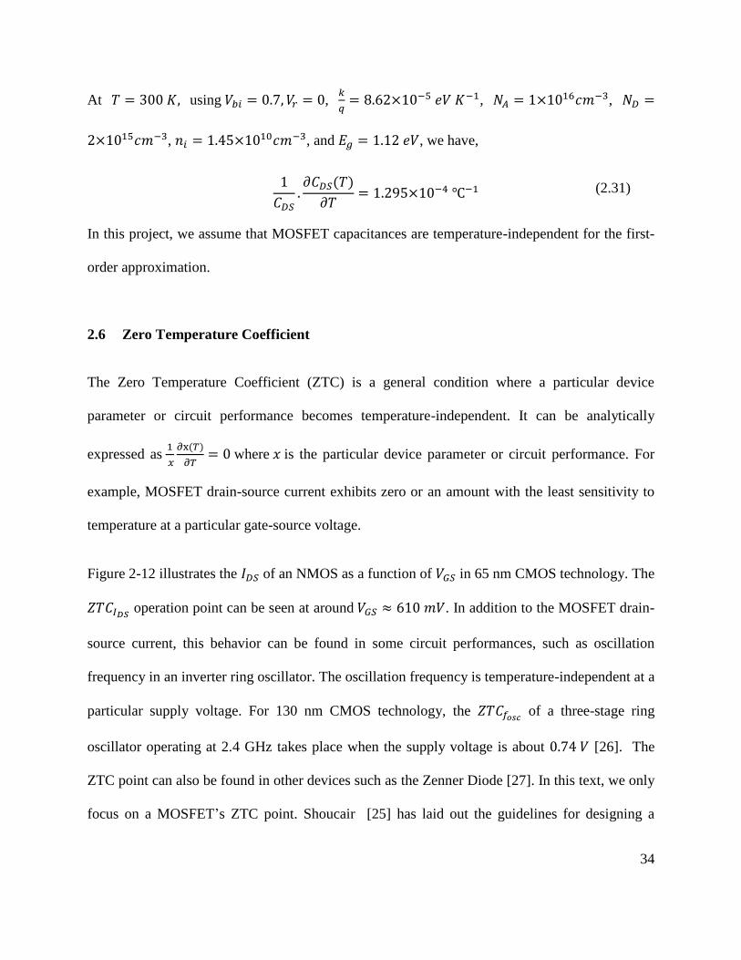
Figure 2-12 illustrates the 𝐼𝐷𝑆 of an NMOS as a function of 𝑉𝐺𝑆 in 65 nm CMOS technology. The
𝑍𝑇𝐶𝐼𝐷𝑆 operation point can be seen at around 𝑉𝐺𝑆 ≈ 610 𝑚𝑉. In addition to the MOSFET drain-
source current, this behavior can be found in some circuit performances, such as oscillation
frequency in an inverter ring oscillator. The oscillation frequency is temperature-independent at a
particular supply voltage. For 130 nm CMOS technology, the 𝑍𝑇𝐶𝑓𝑜𝑠𝑐 of a three-stage ring
oscillator operating at 2.4 GHz takes place when the supply voltage is about 0.74 𝑉 [26]. The
ZTC point can also be found in other devices such as the Zenner Diode [27]. In this text, we only
focus on a MOSFET’s ZTC point. Shoucair [25] has laid out the guidelines for designing a

35
temperature-independent two-stage topology of a CMOS op-amp. In [28] and [29], the 𝑍𝑇𝐶𝐼𝐷𝑆
bias point was reported for the first time, in both linear and saturation regimes. Analytical and
experimental results were presented to obtain the accurate 𝑍𝑇𝐶𝐼𝐷𝑆 bias point in CMOS technology.
Osman [30] also obtained a more accurate 𝑍𝑇𝐶𝐼𝐷𝑆 point considering the temperature dependency
of mobility degradation within a vertical field.
µ𝑒𝑓𝑓(𝑇) =µ𝑜
1 + 𝜃(𝑇). (𝑉𝐺𝑆 − 𝑉𝑡ℎ(𝑇)) (2.32)
where µ𝑜 denotes low-field mobility and 𝜃(𝑇) is a fitting parameter representing the applied
transverse electric field. Although remarkable efforts have been undertaken to improve the
accuracy of the 𝑍𝑇𝐶𝐼𝐷𝑆 by considering temperature dependence of all model parameters (such as
𝑉𝑡ℎ, µ, 𝜃 and contact resistances), all of the presented equations are not user friendly for analog
Figure 2-12 Simulation results of IDS –– VGS characteristic at VDS = 0.6 V and at various temperatures (in
TSMC 65nm).

36
design purposes [24]. 𝑍𝑇𝐶𝐼𝐷𝑆 can be interpreted as the bias point that compensates for the threshold
voltage shift when temperature mobility is reduced. This intuitive interpretation was made by
Filanovsky [31], who extracted a simple equation for the 𝑍𝑇𝐶𝐼𝐷𝑆 . Ignoring the higher order non-
ideality, such as velocity saturation, we perform a simplified analysis from [31] to obtain the
MOSFET drain-source current in the deep triode region as,
𝐼𝐷𝑆 ≈ 𝜇𝑛𝐶𝑜𝑥 (𝑊
𝐿) (𝑉𝐺𝑆 − 𝑉𝑡ℎ)𝑉𝐷𝑆 𝑓𝑜𝑟 𝑉𝐷𝑆 ≪ (𝑉𝐺𝑆 − 𝑉𝑡ℎ)
(2.33)
We substitute the temperature-dependent expressions for mobility and threshold voltage in the
current equation [24],
𝐼𝐷𝑆 = µ𝑜 (𝑇
𝑇𝑜)−𝑛
𝐶𝑜𝑥 (𝑊
𝐿) (𝑉𝐺𝑆 − 𝑉𝑡ℎ𝑜 + 𝛼𝑉𝑡ℎ(𝑇 − 𝑇𝑜))𝑉𝐷𝑆
(2.34)
→ 𝐼𝐷𝑆 = µ𝑜 (𝑇
𝑇𝑜)−𝑛
𝐶𝑜𝑥 (𝑊
𝐿) (𝑉𝐺𝑆 − 𝑉𝑡ℎ𝑜)𝑉𝐷𝑆 + µ𝑜 (
𝑇
𝑇𝑜)−𝑛
𝐶𝑜𝑥 (𝑊
𝐿) 𝛼𝑉𝑡ℎ𝑇𝑉𝐷𝑆 −
µ𝑜 (𝑇
𝑇𝑜)−𝑛
𝐶𝑜𝑥 (𝑊
𝐿)𝛼𝑉𝑡ℎ𝑇𝑜𝑉𝐷𝑆
(2.35)
Thus we have,
𝜕𝐼𝐷𝑆
𝜕𝑇= µ𝑜 (
1
𝑇𝑜)−𝑛(−𝑛𝑇−𝑛−1)𝐶𝑜𝑥 (
𝑊
𝐿) (𝑉𝐺𝑆 − 𝑉𝑡ℎ𝑜)𝑉𝐷𝑆 +
µ𝑜 (1
𝑇𝑜)−𝑛(−𝑛𝑇−𝑛−1) 𝐶𝑜𝑥 (
𝑊
𝐿)𝛼𝑉𝑡ℎ𝑇𝑉𝐷𝑆 + µ𝑜 (
𝑇
𝑇𝑜)−𝑛
𝐶𝑜𝑥 (𝑊
𝐿) 𝛼𝑉𝑡ℎ𝑉𝐷𝑆 −
µ𝑜 (1
𝑇𝑜)−𝑛(−𝑛𝑇−𝑛−1) 𝐶𝑜𝑥 (
𝑊
𝐿)𝛼𝑉𝑡ℎ𝑇𝑜𝑉𝐷𝑆 = µ𝑜𝐶𝑜𝑥 (
𝑊
𝐿) (
𝑇
𝑇𝑜)−𝑛
[−𝑛
𝑇(𝑉𝐺𝑆 −
𝑉𝑡ℎ𝑜) + 𝛼𝑉𝑡ℎ (1 − 𝑛 +𝑛𝑇𝑂
𝑇)] 𝑉𝐷𝑆
(2.36)
Based on the ZTC bias point definition (𝜕𝐼𝐷𝑆(𝑇)
𝜕𝑇= 0), at the bias in which the drain-source current
exhibits zero variation with temperature, we can obtain a 𝑉𝐺𝑆 value that corresponds to the ZTC
as,

37
𝑉𝐺𝑆(𝑍𝑇𝐶) = 𝑉𝑡ℎ(𝑇) +𝑇𝛼𝑉𝑡ℎ𝑛
(2.37)
𝐼𝐷𝑆 =µ𝑜𝑇𝑜
2𝐶𝑜𝑥2
(𝑊
𝐿)𝛼𝑉𝑡ℎ
2 (2.38)
As a result, for 65nm technology we can see 𝑉𝐺𝑆(𝑍𝑇𝐶) ≈ 0.55 𝑉 by taking 𝛼𝑉𝑡ℎ =
0.7𝑚𝑉 𝐾−1 and 𝑉𝑡ℎ = 0.4 𝑉. It can be shown that there exists two separate 𝑍𝑇𝐶𝐼𝐷𝑆 for a MOSFET;
one located within the saturation, and one within the linear region.
We also define the 𝑍𝑇𝐶𝑔𝑚 point, when the transconductance (𝑔𝑚 –– 𝑉𝐺𝑆) characteristics of the
MOSFET remain constant when temperature varies, as 𝜕gm(𝑇)
𝜕𝑇= 0. Figure 2-13 depicts the 𝑔𝑚 of
an NMOS as a function of 𝑉𝐺𝑆 in 65 nm CMOS technology. The 𝑍𝑇𝐶𝑔𝑚 operation point can be
seen around 𝑉𝐺𝑆 ≈ 420 𝑚𝑉 for an NMOS transistor.
Figure 2-13 Simulation results of gm –– VGS characteristics at VDS=0.6 V and at various temperatures (in
TSMC 65nm).

38
The 𝑍𝑇𝐶𝑔𝑚 and 𝑍𝑇𝐶𝐼𝐷𝑆 can be utilized in analog circuit design for high temperature applications.
For example, 𝑍𝑇𝐶𝑔𝑚can be used to achieve stable circuit parameters while 𝑍𝑇𝐶𝐼𝐷𝑆can be used to
maintain the DC bias current. We note that 𝑍𝑇𝐶𝑔𝑚 and 𝑍𝑇𝐶𝐼𝐷𝑆 are highly process-dependent and
we can not obtain both conditions together [32].
2.7 Conclusion
In this chapter we have provided a lump model for passive devices in standard CMOS technology.
The inductor can be modelled as an RLC circuit whose resistances are temperature-dependent
while the inductance and parasitic capacitances are temperature-independent. At frequencies
below 2 𝐺𝐻𝑧, the parasitic resistance increases and quality factor decreases, while at high
frequencies and high temperature the quality factor increases with increasing temperature.
Silicon is inherently temperature dependent. The threshold voltage, mobility, and substrate leakage
current are the most important temperature-dependent parameters. A MOSFET current can exhibit
positive, negative or zero-temperature-coefficients. Therefore, temperature effects can be
minimized by properly biasing a transistor around the ZTC point. Similar to Shoucair [25], we
can follow guidelines for designing temperature-independent circuits. We see that ZTC
characteristics can be employed to design a temperature-independent circuitry.

39
Chapter 3: Low-Power VCO for Biomedical Application
In this chapter, we briefly discuss basic oscillator concepts, particularly focusing on LC-VCOs
(voltage-controlled oscillators). We will also present a brief discussion of the effects of
temperature on the operation of LC-VCOs, and we propose a low power VCO/buffer that can be
used for implantable biomedical applications. We will show that the proposed circuit can be used
for OOK-pulse width modulation systems, and with circuit modification it is capable of being used
in phase modulation systems as well.
3.1 RLC Circuit
An ideal LC (lossless) circuit is shown in Figure 3-1. Assuming an impulse current is applied to
the circuit, based on the law of conservation of energy the total energy at any point of time is
constant and equal to the initial energy stored in the capacitor. That is, in an LC circuit the energy
is only exchanged between capacitor and inductor. From the circuit’s point of view, the capacitor
voltage can be obtained as,
𝜕2𝑣𝑐𝜕𝑡2
+1
𝐿𝐶𝑣𝑐 = 0
𝐿𝑎𝑝𝑙𝑎𝑐𝑒 𝑡𝑟𝑎𝑛𝑠𝑓𝑜𝑟𝑚→ 𝑠2 +
1
𝐿𝐶= 0
(3.1)
𝑠1,2 = ±𝑗
√𝐿𝐶= ±𝑗𝜔𝑜 (3.2)
𝑠1,2 = ±𝑗
√𝐿𝐶= ±𝑗𝜔𝑜 (3.3)

40
As mentioned previously, in practice both the capacitor and inductor are lossy. For simplicity, we
model the total loss as a parallel resistor as shown in Figure 3-2. In this case, the energy is
exchanged between capacitor and inductor, albeit at a lower rate 𝜔𝑑 , eventually decaying to zero.
𝜕2𝑣𝑐𝜕𝑡2
+1
𝑅𝐶
𝜕𝑣𝑐𝜕𝑡+1
𝐿𝐶𝑣𝑐 = 0
𝐿𝑎𝑝𝑙𝑎𝑐𝑒 𝑡𝑟𝑎𝑛𝑠𝑓𝑜𝑟𝑚→ 𝑠2 +
1
𝑅𝐶𝑠 +
1
𝐿𝐶= 0
(3.4)
𝑠1,2 = 𝛼 ± 𝑗𝜔𝑑 = −𝜔𝑜2𝑄± 𝑗𝜔𝑜√1 −
1
4𝑄2 (𝑤ℎ𝑒𝑟𝑒 𝑄 =
𝑅
𝐿𝜔𝑜= 𝑅𝐶𝜔𝑜 (3.5)
→ 𝑣𝑐(𝑡) = 𝑉𝑂 𝜔𝑜𝜔𝑑e−αt cos(𝜔𝑑𝑡 + cos
−1𝜔𝑑𝜔𝑜) (3.6)
LC
+
-
VC(t)
Energy
ωot
½ CVo2
π/2 π
σ
jω
Figure 3-1 Ideal LC circuit (left), Capacitor energy in an ideal LC circuit (center), Pole locations of an LC
circuit in the s-plane (right).
LC
+
-
VC(t)
Energy
ωot
½ CVo2
π/2 π
σ
jω
-α
jωd
R-jωd
e-2αt
Figure 3-2 Lossy LC circuit (left), Capacitor energy in lossy LC circuit (center), Pole locations of an RLC
circuit in the s-plane (right).
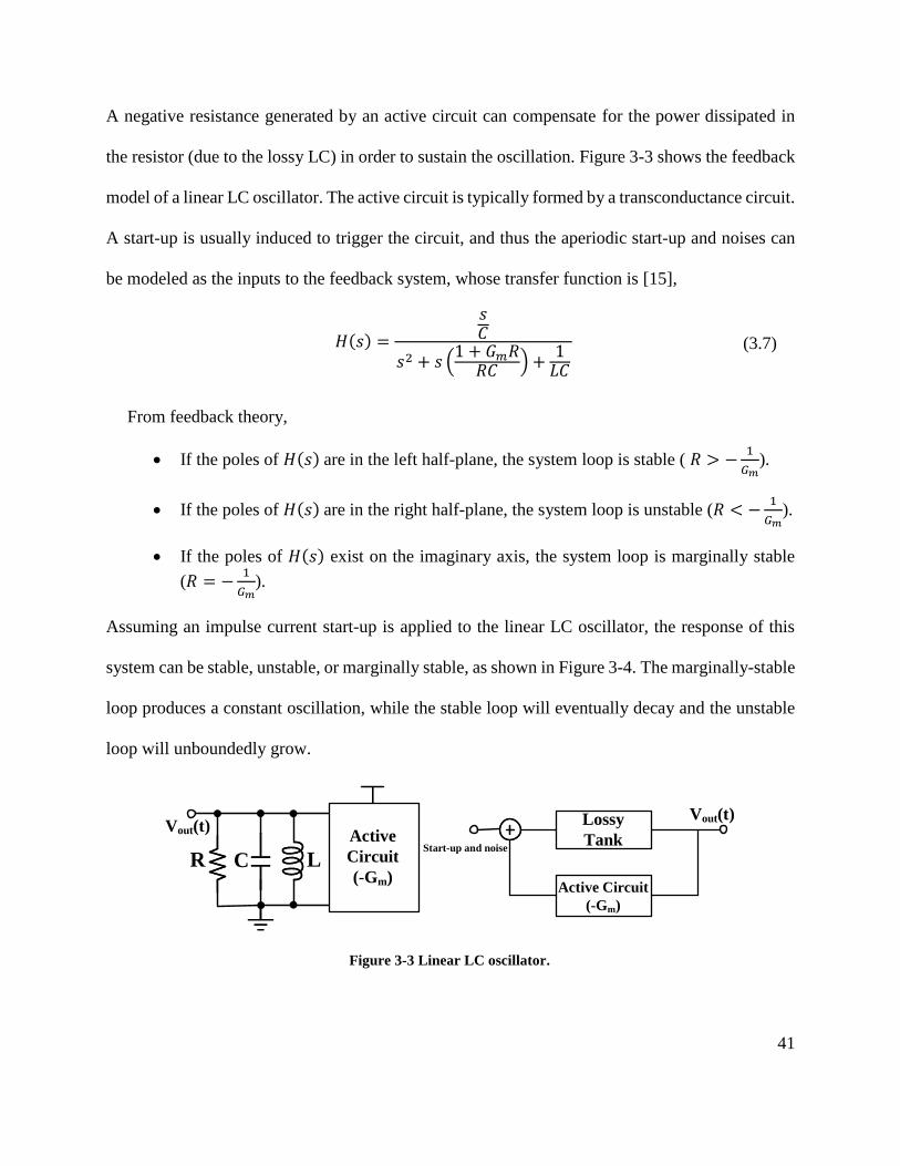
41
A negative resistance generated by an active circuit can compensate for the power dissipated in
the resistor (due to the lossy LC) in order to sustain the oscillation. Figure 3-3 shows the feedback
model of a linear LC oscillator. The active circuit is typically formed by a transconductance circuit.
A start-up is usually induced to trigger the circuit, and thus the aperiodic start-up and noises can
be modeled as the inputs to the feedback system, whose transfer function is [15],
𝐻(𝑠) =
𝑠𝐶
𝑠2 + 𝑠 (1 + 𝐺𝑚𝑅𝑅𝐶
) +1𝐿𝐶
(3.7)
From feedback theory,
• If the poles of 𝐻(𝑠) are in the left half-plane, the system loop is stable ( 𝑅 > −1
𝐺𝑚).
• If the poles of 𝐻(𝑠) are in the right half-plane, the system loop is unstable (𝑅 < −1
𝐺𝑚).
• If the poles of 𝐻(𝑠) exist on the imaginary axis, the system loop is marginally stable
(𝑅 = −1
𝐺𝑚).
Assuming an impulse current start-up is applied to the linear LC oscillator, the response of this
system can be stable, unstable, or marginally stable, as shown in Figure 3-4. The marginally-stable
loop produces a constant oscillation, while the stable loop will eventually decay and the unstable
loop will unboundedly grow.
LCR
Lossy
Tank
Active Circuit
(-Gm)
Active
Circuit
(-Gm)
Vout(t)
Start-up and noise
Vout(t)
Figure 3-3 Linear LC oscillator.

42
We can also explore the oscillator system in terms of feedback. A negative-feedback amplifier, shown
in Figure 3-5, can oscillate if the 𝐻(𝑠 = 𝑗𝜔1) = −1. That is, the circuit can sustain when the
“Barkhausen’s criteria” are satisfied,
|𝐻(𝑠 = 𝑗𝜔1)| = 1 (3.8)
∡𝐻(𝑠 = 𝑗𝜔1) = 𝜋 (3.9)
3.2 Temperature Effects on LC-VCO
The oscillation frequency of an LC-VCO is commonly assumed as the resonant frequency of the
LC-tank. In practice this is not the case. The oscillation frequency not only changes with energy
losses in the resonator inductor and capacitor, but it is also affected by temperature.
σ
jω
R > -1/Gm R < -1/Gm
R = -1/Gm
Figure 3-4 System pole locations on the pole-zero plot and impulse response of the linear LC oscillator.
H(s)X Y
Figure 3-5 Negative feedback system.

43
As already explained, if the Barkhausen criteria are satisfied then the oscillation is sustained. This
occurs when the loop has a phase shift of 180° and a magnitude of one. In practice, a loop–gain of
greater than one is needed to build up to the steady state, and the amplitude growth will eventually
cease due to the circuit’s nonlinearity. Considering the inductor model and linear LC-oscillator
discussed previously, we simplify the tank as shown in Figure 3-6, where 𝑅𝐿 and 𝑅𝐶 represent the
series resistor due to the losses of the inductor and capacitor, respectively. The effects of
temperature on the active circuit will be discussed in further detail later in this chapter. Currently,
we assume that the active circuit is temperature-independent. Therefore,
𝑍𝐿 = 𝑗𝜔𝐿 + 𝑅𝐿 (3.10)
𝑍𝐶 =1
𝑗𝜔𝐶+ 𝑅𝐶 (3.11)
𝑍𝑜 = 𝑗𝜔𝑀 −1
𝐺𝑚 (𝑃𝑢𝑟𝑒 𝑟𝑒𝑠𝑖𝑡𝑖𝑣𝑒 𝑀 = 0) (3.12)
The operation frequency can be obtained by satisfying the Barkhausen’s criteria,
𝑌𝐶 + 𝑌𝐿 + 𝑌𝑍𝑂 = 𝑌𝑡𝑜𝑡 (3.13)
𝑖𝑚𝑎𝑔 (𝑌𝑡𝑜𝑡) = 0 (3.14)
LC
RC
Act
ive
Cir
cuit
Vout(t) Zo
RL
Figure 3-6 A simplified model of LC-tank.

44
→−𝜔𝐿
𝑅𝐿2 + (𝜔𝐿)2
+
1𝜔𝐶
𝑅𝐶2 +
1(𝜔𝐶)2
= 0 (3.15)
We define the quality factor of the capacitor and inductor as,
𝑄𝐿 =𝜔𝐿
𝑅𝐿 (3.16)
𝑄𝐶 =1
𝑅𝐶𝜔𝐶 (3.17)
Therefore, we can simplify the equation as,
𝜔2𝐿𝐶 =
(1 +1𝑄𝐶2)
(1 +1𝑄𝐿2)
(3.18)
𝜔𝑜 =1
√𝐿𝐶→ 𝜔𝑂𝑆𝐶
2 = 𝜔𝑜2(
(1+1
𝑄𝐶2)
(1+1
𝑄𝐿2)
) (3.19)
This can be further simplified using first order Taylor series expansion,
𝜔𝑂𝑆𝐶2 = 𝜔𝑜
2(1 +1
𝑄𝐶2)(1 −
1
𝑄𝐿2) ≈ 𝜔𝑜
2(1 +1
𝑄𝐶2 −
1
𝑄𝐿2) (3.20)
Evidently, both capacitor and inductor losses will affect the oscillation frequency presented in
equation (3.20). In general, the former causes an increase in oscillation frequency while the latter
decreases oscillation frequency. The quality factor of available capacitors in CMOS 65nm is
usually much greater than that of the inductors at our frequency of interest. Therefore, the equation
can be rewritten as,
𝑄𝐶 ≫ 1 → 𝜔𝑂𝑆𝐶2 ≈ 𝜔𝑜
2(1 −1
𝑄𝐿2) (3.21)

45
We conclude that the oscillation frequency deviates from the resonant frequency due to losses in
the tank. Although we ignore the loss of the capacitor owing to the high Q value, the inductor’s
parasitic resistors can affect the oscillation frequency, as they are highly frequency and
temperature-dependent. As we know, the frequency dependence of the parasitic resistance can be
ignored at frequencies below 1 𝐺𝐻𝑧. From the presented inductor temperature model in the
previous chapter, we establish that as temperature increases, resistance in the spiral metal causes
the quality factor to decrease, while resistance of the substrate improves the quality factor at high
frequencies. In other words, at low frequencies the dominant resistance is a series metal resistor
which linearly increases (or reduces the quality factor) with increasing temperature. Consequently,
the frequency of operation decreases in respect to temperature. At high frequencies, however, the
substrate resistance is dominant. The substrate resistance also increases with temperature (up to a
point). In this case, the quality factor also rises (or the frequency of operation increases) with
increasing temperature. It should be noted that using a large inductor results in large substrate
capacitance and resistances. Therefore, eddy current and displacement current are significant and
cannot be ignored at low frequency. As shown in Figure 3-7 (a), the frequency of oscillation is
linearly increasing, and our simulation shows that at the ISM band, the frequency varies
approximately +/−5% over the range of [−20 140] °C.
We need to also investigate the temperature dependence of the active circuit. For simplicity, we
assume that the active circuit is memory-less, meaning that it contains no reactive or energy-
storage components. In order to sustain the oscillation frequency, the Barkhausen’s criteria should
be satisfied. From our previous discussion, the active circuit must be able to replenish the energy
lost in the tank (𝐺𝑚𝑅 > −1). If this energy conservation requirement is not satisfied, we will

46
observe a growing or decaying oscillation. We know that both the transconductance and the energy
loss (𝑅) are temperature dependent; 𝐺𝑚 reduces (1
Gm increases) while 𝑅 increases with increasing
temperature. Therefore, we can surmise that the temperature effect of an active circuit on
oscillation amplitude and frequency is counterbalanced by tank resistance, which is negligible.
From another point of view, the oscillation amplitude is equal to 𝑅×𝐼, where 𝑅 is the (parallel)
tank resistance and 𝐼 is the fundamental current provided by the active circuit. Assuming that the
current is temperature-independent using the ZTC bias point concept, we expect that the amplitude
will increase as temperature goes up. However, the transconductance decreases and because of the
compressive nature of the active circuit, the oscillation amplitude cannot arbitrarily increase,
resulting in the active circuit attempting to compensate for this increase. We note that in reality
the “large-signal” transconductance must be used instead of the small-signal conductance. In [33]
it is shown that it is practically impossible to achieve a marginally-stable state with small-signal
transconductance in a linear oscillator. Yet the large-signal transcendence does indeed balance the
tank loss in a nonlinear oscillator.
Due to stringent power constraints, large devices should be avoided for biomedical VCOs. As
discussed previously, parasitic capacitances of MOSFET are weakly temperature-dependent, thus
we ignore the temperature dependence of parasitic capacitances.

47
(a)
(b)
Figure 3-7 Simulation results of a VCO frequency vs. Temperature (a) large inductor (after
compensation) (b) small inductor.

48
3.3 Low Power VCO/Buffer for Biomedical Application
We have acknowledged that the main concern of implantable biomedical devices is the power
budget. Such stringent power requirements result in simplified approaches for handling wireless
communication. That is, only the bare necessities are left for the transmitter and receiver. It is
practically impossible to use a power amplifier in an implantable biomedical system to drive the
load. On the other hand, if the VCO is directly connected to an antenna, the hostile environment
of the body could affect oscillation frequency. Thus, a buffer could potentially help to enhance
drivability and could provide a reverse isolation for the LC-VCO. In this case we must note that a
buffer dissipates power and increases the total power consumption. Therefore, it makes sense to
employ the current re-use technique to meet the power budget. We propose a LC-oscillator/buffer
with enhanced load drivability.
Total power consumption can be reduced by sharing the current between circuits. In our circuit,
the current is shared between an NMOS-only LC-VCO and a common source buffer. Using an ac
coupling network, containing 𝑅2 and 𝐶2, the buffer can be dc-isolated from the VCO while the
signal can pass through. A decoupling capacitor (𝐶𝐷) is also used to avoid any coupling, especially
noise, between the VCO and buffer. It should be noted that the supply noise coupled to the
oscillator is lower than the conventional NMOS-only oscillator. This is due to the voltage division
between the buffer and oscillator.
The buffer is capable of driving of a 50 𝛺 load and can withstand a large capacitive load.
Additionally, it can provide an adequate output swing while isolating the LC tank and load. Figure
3-8 illustrates the schematic of this circuit.

49
Although an off-chip bias voltage 𝑉𝐵 is used to explore and improve the effect of temperature on
the LC-oscillator, one can instead use a conventional NMOS-only oscillator to decrease the area
at a cost of higher temperature decency. Simulation results show that an accurate bias voltage 𝑉𝐵
can significantly enhance the temperature and supply voltage effects on the oscillator. Simulations
show that the frequency of a conventional NMOS-only oscillator varies up to 650 𝑀𝐻𝑧/𝑉 with
an increasing supply voltage, while our circuit varies by only 80 𝑀𝐻𝑧/𝑉.
VB (Temp.)
M3M4
L1 L1
C2 C2
R2 R2
L2 L2C3 C3
M1M2
C1
R1
C1
R1
CD
C4 C4
cc
VD
SW1
CLK
SW1
CLK
CL RLCLRL
Figure 3-8 Proposed LC-oscillator/buffer schematic.

50
In Figure 3-8, transistors 𝑀3 and 𝑀4 are loaded with an inductor to maximize the output swing
and to provide the matching network. Moreover, the body-source of 𝑀3 and 𝑀4 are tied to ensure
that there is no nonlinearity caused by the body’s effect.
From our previous discussion in chapter 2, we see that 𝑉𝐷 is designed in such a way to be
approximately 0.4 𝑉 in order to minimize temperature’s effect on the transconductance of NMOS
transistors. The temperature coefficient of the oscillator frequency is about −0.3 𝑀𝐻𝑧/. If a
well-regulated supply voltage is not available, one can improve efficiency using a tail current
combined with Hegazi’s technique for noise reduction at the cost of output swing, higher supply
voltage, and higher power consumption. However, our priority here is to minimize power
consumption and maximize the output swing. In consequence, the bias current source is not being
used.
Patterned ground shield (PSG) planar spiral inductors are also employed. As discussed previously,
PSG can improve the effect of temperature on the inductor by reducing capacitive coupling to the
substrate. The quality factor and inductor values remain relatively constant at the ISM band
frequency. That said, differential inductors can be used in order to enhance the quality factor and
area efficiency.
The VCO-buffer is fabricated in CMOS 65 nm technology (Figure 3-9). The die size is
690× 670 𝜇𝑚2 and the power dissipation is approximately 115 µ𝑊 at 0.6 𝑉 (minimum supply
voltage). The buffer is connected to the load with wire bond (dashed-line). The output capacitance
(𝐶𝐿) includes the parasitics from the PCB trace and bond wire. The output signal power is
approximately −31 𝑑𝐵𝑚 at 0.6 𝑉 supply voltage. The simulation shows that the phase noise is
51
−110 𝑑𝐵𝑐/𝐻𝑧 at 1 𝑀𝐻𝑧 offset. The key performance metrics and a comparison with other low
power oscillators for biomedical applications are summarized in Table 3-1.
The proposed VCO-buffer uses an NMOS-based source-follower buffer stacked on top of an
NMOS-only oscillator. It can directly connect to a 50 Ω load. This is used for a pulse width
modulation-on/off keying (PWM-OOK) system for the implantable biomedical transmitter. In
order to bring the leakage power down, power gating can be applied to all blocks (temperature
sensor and transmitter) using thick oxide NMOS/PMOS switches. Additionally, low 𝑉𝑇ℎ
transmission-gate switches at the output of the buffer are used to implement the OOK system.
Given the low output load (50 𝛺), wide transistors should be employed to prevent degrading the
signal transmission; although, smaller switches can be used at the cost of higher ripple and
performance degradation. Charging and discharging of these wide transistors may also be
problematic, and careful consideration is required − i.e. to improve switch performance, a voltage
booster for the clock can be used.
As discussed previously, phase modulation has improved noise performance compared to
amplitude or frequency modulation. However, phase modulation requires an additional mixer or
balun. Active mixers increase power consumption, while passive mixers suffer from low gain and
degrade efficiency. In addition, a major problem associated with a passive mixer is the
temperature-dependence of MOS switches, which can considerably reduce the signal delivered to
the load.

52
Performance This work [62] [34] [63]
Supply (V) ≥ 0.6 V 0.56 0.7 1.8
Power 115 µ𝑊 150 350 840
Frequency (MHz) 965 (@0.6V) 𝑀𝐼𝐶𝑆 𝑀𝐼𝐶𝑆 𝑀𝑒𝑑𝑅𝑎𝑑𝑖𝑜
Output signal
power (𝑑𝐵𝑚) −31 −16 −16 −17.19
Modulation PWM/OOK OOK MSK/OOK 𝑂𝑂𝐾
Area (𝑚𝑚2) 0.46 − 0.5 0.55
Technology 65 nm CMOS 65 𝑛𝑚 𝐶𝑀𝑂𝑆 90 𝑛𝑚 𝐶𝑀𝑂𝑆 180 𝑛𝑚 𝐶𝑀𝑂𝑆
Table 3-1 Performance comparison of OOK transmitter.
690 µm
67
0 µ
m
PCB
Wire-bond
Figure 3-9 Die photo of the proposed VCO/buffer.

53
Figure 3-10 Simulation results of the proposed PWM-OOK TX.
8.5 mV
1.2 V
Data
Signal (single ended)
D.E.
Figure 3-11 Measurement results of the proposed PWM-OOK TX.

54
3.4 Conclusion
The principle of an oscillator from the perspective of circuit point and feedback has been discussed
in this section. We have explained that oscillation can sustain if the Barkhausen’s criteria is
satisfied, or similarly, when the active circuit counterbalances tank loss. We have shown that, in
practice, the frequency of oscillation shifts away from the resonant frequency of the LC-tank due
to inductor and capacitor losses. We also have seen that the parasitic resistors are temperature-
dependent, as well as the frequency of oscillation; the oscillation frequency will decrease with
increasing temperature. That said, at high frequencies and high temperatures, the oscillation
frequency increases as temperature increases. This occurs due to the displacement and eddy
currents in the substrate. We have proposed a practical circuit that minimizes the effect of
temperature while achieving high performance for low-power application.

55
Chapter 4: A Low-Power Temperature Sensing System for Implantable
Biomedical Applications
Chapter 5
This chapter presents a low-power system that senses ambient temperature and wirelessly
transmits the sensed information to a nearby receiver. Although intended for an implantable smart
coronary stent, it can be used for other sensory applications that require similar temperature
sensing. A thermal sensor is presented that utilizes MOSFET’s biased in sub-threshold along with
a combination of p+-poly and n+-poly resistors to generate a PTAT (proportional to absolute
temperature) source that can operate at low supply voltages. Leveraging the central limit theorem,
the output currents of several PTAT sources are combined to further reduce error. The resulting
PTAT source is then used to implement a temperature-controlled oscillator for frequency
modulation and transmission. A prototype in 65-nm CMOS can sense and transmit temperature
values in the range of 30 to 50 °𝐶, with an average resolution of 1.1 𝑀𝐻𝑧/°𝐶. The sensor-
transmitter system consumes 100 𝜇𝑊 of DC power and delivers −34 𝑑𝐵𝑚 of power to a 50 − Ω
load.
4.1 Introduction
Recent technological advances in integrated circuits (ICs) and wireless communications have
revolutionized the realization of implantable sensors for health monitoring and diagnosis, and
biomedical wireless telemetry [34]–[36]. We know that in practice, an implantable sensor should
be small and should operate robustly inside the human body with reasonable operation longevity.
Thus, the design of such a sensor and its wireless telemetry system is also driven by the

56
aforementioned traits of simplicity, having a small footprint, being lightweight, operating at low-
power, and having efficient transmitter (TX) architecture.
The work presented here is intended for an implantable smart coronary stent. To clarify, a stent is
a mesh-like tube which is inserted into a blocked or a narrowed artery site to keep the lumen open.
Conventional stents can be considered as passive elements. Recently, a class of intelligent active
stents have been proposed that can be remotely heated with wireless control of their temperature.
Such stents enable wireless endo-hyperthermia, which facilitates inhibition of in-stent restenosis
(re-narrowing of the stented location) [37], [38]. In other words, they use moderate local heating
to prevent restenosis by limiting cell proliferation [37]. To remotely warm up the stent, power is
harvested from a dedicated radio frequency (RF) source that is outside of the patient’s body and is
converted to heat. However, if there is no control over such heating, a thermal runaway may incur,
leading to adverse effects [38]. Therefore, a robust implantable temperature sensor (TS) is required
for monitoring and controlling temperature.
Although modern CMOS IC technology has made it feasible to realize small-size TSs, they are
typically power hungry, require relatively high supply voltages (𝑉𝐷𝐷), and are rather inaccurate,
preventing their widespread use. In this work, we present a low-power TS along with a low-power
915 𝑀𝐻𝑧 frequency-modulated (FM) TX (Figure 4-1). The proposed system is designed to use
the stent as an antenna for data communication. The stent is also used for energy harvesting (the
energy harvesting unit is outside the scope of this paper). Temperature data is FM-modulated using
a temperature-varying capacitor which sets the frequency of a temperature-controlled oscillator
(TCO). The proposed system is designed and fabricated in a 65-nm CMOS process. Measurement
results show that the prototype offers an average resolution of 1.1 𝑀𝐻𝑧/°𝐶 and senses temperature

57
changes in the specified range of 30 to 50 °𝐶. The TX dissipates 100 𝜇𝑊 of DC power while
delivering −34 𝑑𝐵𝑚 of power to a 50 − Ω antenna.
In this chapter, the proposed TS and FM TX circuit are described. Measurement results are
presented and concluding remarks are also provided.
4.2 Temperature Sensor Architecture
Due to the high level of integration, low cost, and digital signal processing capabilities of CMOS
technology, CMOS-compatible sensors are attractive for biomedical implants. Physical and
electrical properties of silicon, which are temperature-dependent, can be exploited to implement a
TS. For instance, MOSFET’s threshold voltage (𝑉𝑇ℎ) and mobility (𝜇) have a negative temperature
Cvar
Power Link Data Link
Stent
Temperature
Sensor
Body
T = 37oC T = 38
oCT = 36
oC
Figure 4-1 A temperature sensor and transmitter for smart-stent implants.

58
coefficient (TC). Also, parasitic PNP and NPN bipolar junction transistors (BJTs) in CMOS
technology can be used for TS. However, BJT-based TSs operate at a relatively higher 𝑉𝐷𝐷, posing
serious power limitations for a single-supply implantable system that is often powered through
energy harvesting. Low-power CMOS-based TSs on the other hand suffer from increased
nonlinearity and errors.
Figure 4-2 shows the proposed low-power CMOS TS operating at 𝑉𝐷𝐷 = 0.6 𝑉. The sensor uses
thick-oxide MOS devices (to minimize leakage) that are biased in the subthreshold region. In this
region, the drain current of a transistor can be written as;
𝐼𝐷 ≈ µ0COXW
LVT2(ζ − 1)e
VGS−Vthζ𝑉𝑇 (5.1)
Figure 4-2 Proposed low-power CMOS-based temperature sensor.
VDD
RN-Poly
RP-Poly
MN2MN1
MP1 MP2
RP-Poly
Temp.
RN-Poly
Temp.
RN-Poly+RP-Poly
Temp.
TS 1
TS 2
TS N
Temp.
SignalIOUT
IIN
IOUT α T
TS
Temperature
sensor

59
where 𝑉𝑇 is the thermal voltage (=KT
q ~ 25𝑚𝑉/°𝐶) and ζ is a parameter that represents the
capacitive coupling between the gate and silicon surface. The output current of the TS can be
written as:
𝐼𝑜𝑢𝑡 = VGSN1 − VGSN2RP,Poly + RN,Poly
=VGSN1 − VGSN2
Req (5.2)
Using (5.1) and (5.2), and assuming that all transistors use the same lengths, 𝐼𝑜𝑢𝑡 can be simplified
as:
𝐼𝑜𝑢𝑡 = ζVTReq
× ln (WP1WN2WP2WN1
) (5.3)
In (5.3), there are still two main parameters, namely, VT and Req, that are temperature
dependent. The TC of a poly-resistance can be made positive or negative depending on its doping
Figure 4-3 Output current versus temperature for the proposed sensor.

60
[39]. Thus, as shown in Figure 4-3, a series combination of p+-poly and n+-poly-resistances can,
to the first order, equalize the dependency of Req to temperature. Figure 4-3 shows the simulated
𝐼𝑜𝑢𝑡 versus temperature for the proposed TS. As can be seen from the figure, within the temperature
range of 30 to 50 °𝐶 (which exceeds that of the human body), the curve is relatively linear with a
resolution of approximately 5 𝑛𝐴/°𝐶. However, for robust operation, a higher order of temperature
dependency, along with process variations and mismatches, must be taken into account. It should
be noted that TS linearity specifications for implantable devices are not as stringent as other
thermal sensors [40]–[42] due to the relatively narrow range of operating temperatures within the
human body. Thus, as compared to one highly-linear and accurate sensor consuming large power
and area, we implement multiple TSs that are ultra-compact, operate at low 𝑉𝐷𝐷, and consume ultra
low power. According to the central limit theorem, the sum of many independent random variables
tend to be distributed according to one of a small set of attractor distributions [43]. In this design,
ten TSs are distributed on the chip to ensure that the adverse effects of the process variation will
also be averaged out and the desired accuracy will be obtained. As each TS consumes 0.2 𝜇𝑊
(worst case at about 50 °𝐶) and occupies 0.0004 𝑚𝑚2, operating all ten TSs is preferred over
choosing the best single TS, as this avoids complex calibration schemes. For the sake of
completeness, Figure 4-4 compares the performance of the proposed TS with state-of-the-art
designs, keeping in mind that the different temperature sensing requirements of this work.

61
4.3 Low-Power FM Transmitter
Figure 4-4 shows the proposed transmitter where an FM transmission is selected over amplitude-
modulated (AM) schemes due to its superior noise immunity. The aggregated TS output current
of is first amplified, integrated, and converted to a voltage. Chopping is used to improve the offset
and noise performance. Next, the resulting voltage signal is then used in the second stage to change
the value of a varactor. The combination of the TS, the integrator, and the varactor is equivalent
to a temperature-variable-capacitor (TVC), whose capacitance (𝐶𝑉𝑎𝑟) can be approximately shown
as:
𝐶𝑉𝑎𝑟 =
𝐶𝑉0
(1 +𝜅𝑇𝑇0)𝑚
(5.4)
where 𝐶𝑉0is the capacitance at room temperature, 𝑇0 = 273 °𝐾, m is an empirical fitting parameter
for the varactor, and 𝜅 is a parameter dependent on the gain of the preamplifier. Utilizing the TVC
Parameter This work [41] [40] [42]
Technology 65 nm CMOS
0.16 μm
CMOS
65nm CMOS
0.5 μm SOI
BiCMOS
VDD (V) 0.6 1.5 1.2 5
Error (oC) ±0.8 ±0.06 ≈ ± 2.8 ±0.6
Temperature (oC) 30 ~ 50 -55 ~ 125 -40 ~ 120 -70 ~ 225
Sensor Type Subthreshold BJT Ring Oscillator Thermal Diffusivity
Area (mm2) 10*0.0004 0.16 0.0013 1
Power (μW) 10*0.12 6.9 400 3.5
Table 4-1 Temperature sensor performance summary and comparison.

62
in the resonant tank of an LC oscillator results in a TCO, whose operating frequency is expressed
as:
𝑓𝑜𝑠𝑐 =1
2𝜋 √𝐿𝑇(𝐶𝑇 + 𝐶𝑉𝑎𝑟) (5.5)
As the minimum attenuation of body tissue on RF signals occurs in the frequency range of
0.8 ~ 1 𝐺𝐻𝑧 [38], the resonant tank of the TCO is tuned at a center frequency of 915 𝑀𝐻𝑧 (Figure
4-6), which is also within an unlicensed Industrial, Scientific, and Medical (ISM) band. It can be
shown that for the given oscillator, the bias current, 𝐼𝑏𝑖𝑎𝑠, is inversely proportional to the product
Cvar
LTank
Stent
M1
M2
Cd
Rf
VDD
gmp
gmn
VoutAB
A B
C
TS N
Temp.
Sensors
Push-Pull PA
ΦCh ΦCh
+
−
RST
VDD
M1 M2
M3 M4
ΦCh ΦCh ΦCh
=
LPF
Vin-
Vin+
VDD
VB1
CC RC
Vout
ΦCh
Chopper
TS 1
TS 2
CMOS
VCO
Chopper-Stabilized
Op-Amp
Data LinkT = 37
oCT = 36
oC T = 38
oC
Figure 4-4 Proposed FM transmitter.

63
of the tank quality factor (𝑄𝑇) and inductance (𝐿𝑇) [44]. As a result, in this design we have
maximized 𝑄𝑇𝐿𝑇 at 915 𝑀𝐻𝑧 to minimize the power consumption.
Through 3𝐷 electromagnetic simulations, an optimized 𝐿𝑇 of 180 𝑛𝐻 at 915 𝑀𝐻𝑧 is designed
with a 𝑄𝑇 of about 5. Using this overall power consumption, the TCO is minimized to ~120 𝜇𝐴.
To ensure that 𝑓𝑜𝑠𝑐 varies predominantly due to temperature change sensed by the TS, an on-chip
low-dropout (LDO) regulator with 30 𝑑𝐵 of supply rejection and up to 100 𝑚𝑉 of dropout is used
to generate a 𝑉𝐷𝐷 of 0.6 𝑉 (from a harvested supply of 0.7 𝑉) for the LC oscillator, and small
cross-coupled devices in the oscillator core are used to minimize their parasitic capacitance.
However, the relatively large inductor represents a resistive loss in the inductor 𝑅𝐿, which can also
introduce a positive TC to the oscillation frequency. The substrate capacitance is also temperature-
dependent, but its variations are negligible for microstrip structures operating at the frequency of
about 1 𝐺𝐻𝑧. In many industrial temperature sensors, a robust system must have the ability to
function within a broad temperature range (typically, – 40 °𝐶 to 125 °𝐶) and the effect of
temperature on the series resistance and substrate capacitance should be considered. Biomedical
sensors do need to operate within a much lower temperature range (e.g., 30 to 50 °𝐶), and thus,
adverse effects of temperature variations are less pronounced. We have co-designed the TSs and
LC oscillator over the operating temperature range of this application (30 to 50 °𝐶) to meet the
desired resolution and error requirements. The output of the TCO is connected to two current-re-
used push-pull [45] amplifiers to drive the stent. For our proof-of-concept prototype, the active
stent impedance is chosen to be 50 𝛺 at 915 𝑀𝐻𝑧. The push-pull amplifier delivers 3.8 𝜇𝑊 of RF
power to the stent, large enough to be detected with a sensitive external reader circuit.

64
4.4 Measurement Results
As a proof-of-concept, the proposed low-power sensor along with the FM-modulator is designed
and laid out in a 65-nm CMOS process. Figure 5-5 shows a die micrograph with a total area of 700
m × 350 m. Figure 4-5 demonstrates transmitted output frequency versus temperature. As can
be seen in Figure 5-6, for the temperature range of 30 to 50 °C, the TX tunes the output frequency
by 1.1 𝑀𝐻𝑧/°𝐶. shows the output frequency of the TX at 914.4 and 926.5 𝑀𝐻𝑧 with the peak
output power of – 24.48 and – 24.62 𝑑𝐵𝑚 to a 50 − 𝛺 load, respectively. The overall power
consumption of the TX is 100 𝜇𝑊. Measurement results of the TX along with a comparison with
prior-art TX designs are tabulated in Table 4-2.
4.5 Conclusion
An ultra-low-power ultra-compact low-voltage TS is implemented using a combination of
MOSFETs and p+/n+ poly resistors. The effects of mismatch, process variations, and other non-
idealities are reduced by using multiple distributed sensors. Driving a varactor in an LC oscillator,
the TSs realize a TCO; temperature variations, therefore, result in an FM TX. Further, a 65-nm
CMOS proof-of-concept prototype has been designed for a smart stent application. Measurement
results show that our proposed technique can tune the output frequency with a resolution of
1.1MHz °C⁄ , when temperature changes from 30 to 50 °C.
700 µm35
0 µ
m
Figure 4-5 Chip micrograph.

65
Figure 4-6 Measured TCO frequency versus temperature.
Parameter
This work [1] [2] [3] [15]
Technology 65 nm 90 nm 180 nm 180 65nm
Supply Voltage
0.7
(0.6 after LDO)
0.7 0.7 2.1 to 3.5 0.56
Frequency Band (MHz) 915 ISM MICS MICS 433 ISM MICS
Modulation FM MSK FSK BFSK OOK
Data Rate 10 kb/s 120 kb/s 250 kb/s 800 kb/s 250 kb/s
Output Power (dBm) –24 NA –16 –17 ~ –4 -16
PDC (μW) 100 350 400 > 10,000 150
Table 4-2 Performance summary and comparison.

66
Figure 4-7 Measured TX output at 914.4 MHz (top) and 926.5 MHz (bottom).

67
Chapter 5: Conclusion
The focus of this research is on the design of low-power temperature sensing systems that can be
wirelessly powered, and among other applications, can be used in biomedical implants. Although
intended for an implantable smart coronary stent, the techniques presented in our research can be
used in other sensory applications requiring similar temperature sensing. In [38] the optimum
frequency of operation and the maximum deliverable power for restenosis telemonitoring have
been discussed. Therefore, with a power budget estimation for the telemonitoring system, we have
designed and implemented two separate temperature-sensing systems in a 65-nm CMOS process.
The first system, which employs an analog frequency modulation technique, benefits from a simple
design and its low consumption of power. This system monitors the smart stent temperature with
a supply voltage of 0.7 𝑉 and power consumption of 100 µ𝑊. This system transmits the
temperature data at the ISM band frequency, while offering 1.1 𝑀𝐻𝑧/°𝐶. Higher resolution may
be obtained at the expense of power consumption and receiver complexity.
The focus of the second architecture is on further improving adaptability and drivability of the
proposed system to different loads. Our simulation results show that the second architecture
(PWM-OOK) can achieve higher resolution (0.2 ) while also reducing receiver complexity.
With an ultra-low-power design in mind, the configuration of this second system is based on pulse
width modulation-on/off keying (PWM-OOK) and low head-room analog and digital blocks,
which allow operation of this system with rectified supply voltages as low as 0.6 V. The total
power consumption of such a system with low supply voltage is about 115 µ𝑊. The receiver
system can be implemented by an envelope detector, low noise amplifier, and a counter. In

68
addition, despite the former (FM) system, PWM-OOK is more robust to the process spread. A
calibration may be required to align and synchronize the transmitter and receiver. Trimming the
receiver located outside of the body is much easier than adjusting the transmitter implemented
inside the patient’s body. Further, the PWM-OOK system is less sensitive to the supply voltage
and load variation. Preliminary measurements are performed for this system, and as expected, the
system can indeed provide more efficient transmission in comparison to conventional implantable
systems. Table 5.1 summarizes the performance of the designs proposed in this work.
5.1 Future Works
As the main objective of this work is to monitor temperature, conducting in-vivo tests are
envisioned as one of the main future goals. The proposed smart stent should be implanted inside
live animal test subjects, and the effects of biocompatible coating on the performance of relevant
Performance PWM-OOK FM
Supply ≥ 0.6 𝑉
0.7
(0.6 𝑎𝑓𝑡𝑒𝑟 𝐿𝐷𝑂)
Power (𝜇𝑊) 115 100
Frequency
(MHz) 965 915 𝐼𝑆𝑀
Output signal
power (𝑑𝐵𝑚) −31 – 34
Area (𝜇𝑚^2) 690× 670 700× 350
Technology 65 𝑛𝑚 𝐶𝑀𝑂𝑆 65 𝑛𝑚 𝐶𝑀𝑂𝑆
Table 5-1 Performance summary of the proposed systems.

69
systems should be explored. A reliable connection between systems and the stent is also a subject
of future work.
Design modifications are also envisioned to improve the performance of circuits. As discussed in
Section 0, a robust bias voltage can improve the supply and temperature sensitivity of the system.
Another possible improvement to such a design is to replace the single-ended inductor with a
differential one. Differential inductors lead to smaller chip area and larger power saving.
Moreover, a low dropout voltage regulator can further reduce the supply sensitivity of the PWM-
OOK system. As discussed in Chapter 1, PSK modulation can further be implemented as an
alternative to the proposed OOK system. Owing to its superior noise performance, long distances
between receiver and transmitter can be achieved.
Finally, if a higher resolution for temperate sensors is required, BJT-based TS, presented in
Appendix A can be a possible solution. In addition, all MOSFET-based temperature sensors
presented in [46] can potentially be used.

70
Bibliography
[1] W. H. Ko, “Early History and Challenges of Implantable Electronics.,” ACM J. Emerg.
Technol. Comput. Syst., vol. 8, no. 2, p. 8, Jun. 2012.
[2] M. A. Hannan, S. M. Abbas, S. A. Samad, and A. Hussain, “Modulation Techniques for
Biomedical Implanted Devices and Their Challenges,” Sensors, vol. 12, no. 12, pp. 297–
319, Dec. 2011.
[3] H.-J. Y. · C. van Hoof, Bio-Medical CMOS ICs, vol. 53, no. 9. 2013.
[4] K. Bazaka and M. Jacob, “Implantable Devices: Issues and Challenges,” Electronics, vol.
2, no. 1, pp. 1–34, Dec. 2012.
[5] “IEEE Std C95.3 TM -2002 (R2008) IEEE Recommended Practice for Measurements and
Computations of Radio Frequency Electromagnetic Fields With Respect to Human
Exposure to Such Fields, 100 kHz–300 GHz IEEE International Committee on
Electromagnetic Safety (Standards Coordinating Committee 28 on Non-Ionizing Radiation)
IEEE-SA Standards Board,” 2002.
[6] Y.-H. Joung, “Development of implantable medical devices: from an engineering
perspective.,” Int. Neurourol. J., vol. 17, no. 3, pp. 98–106, Sep. 2013.
[7] “Energy Harvesting from Human Power a roadmap to new research challenges The Energy
Harvesting Network Executive Summary,” 2011. [Online]. Available: http://eh-
network.org/files/human_power.pdf. [Accessed: 01-Jan-2011].
[8] M. Yin and M. Ghovanloo, “Using Pulse Width Modulation for Wireless Transmission of
Neural Signals in a Multichannel Neural Recording System,” in 2007 IEEE International
Symposium on Circuits and Systems, 2007, pp. 3127–3130.
71
[9] D. C. Jeutter, “Overview of Biomedical Telemetry Techniques,” Eng. Med. Biol. Mag., vol.
2, no. 1, pp. 17–24, Mar. 1983.
[10] W. Sansen, B. Puers, and R. Govaerts, “Design and realisation of an ultra-miniature hybrid
for a pressure telemetry capsule,” in Proceedings of International Conference on
Microelectronics, 1984.
[11] K. Van Schuylenbergh, E. Peeters, B. Puers, and W. Sansen, “An implantable telemetric
tonometer for direct intraocular pressure measurements,” in 1st European Conference on
Biomedical Engineering, 1991.
[12] B. Razavi, “RF MICROELECTRONICS Second Edition.”
[13] Yu Cao et al., “Frequency-independent equivalent-circuit model for on-chip spiral
inductors,” IEEE J. Solid-State Circuits, vol. 38, no. 3, pp. 419–426, Mar. 2003.
[14] J. Chen, “On-chip spiral inductor/transformer design and modeling for RF applications,”
Thesis Univ. Cent. florida, p. 124, 2006.
[15] Hooman Darabi, “Radio Frequency Integrated Circuits and Systems - Hooman Darabi -
Google Books.” .
[16] C. P. Yue and S. S. Wong, “On-chip spiral inductors with patterned ground shields for Si-
based RF ICs,” IEEE J. Solid-State Circuits, vol. 33, no. 5, pp. 743–752, May 1998.
[17] R. Groves, D. L. Harame, and D. Jadus, “Temperature dependence of Q and inductance in
spiral inductors fabricated in a silicon-germanium/BiCMOS technology,” IEEE J. Solid-
State Circuits, vol. 32, no. 9, pp. 1455–1459, 1997.
[18] D. He, Jenhao Cheng, and L. Chen, “Global scaling inductor models with temperature
effect,” in 2008 9th International Conference on Solid-State and Integrated-Circuit
Technology, 2008, pp. 520–522.

72
[19] Y. Z. Xu and J. T. Watt, “A Compact Model for Temperature and Frequency Dependence
of Spiral Inductor,” Tech. Proc. 2007 NSTI Nanotechnol. Conf. Trade Show, vol. 3, pp.
674–677, 2007.
[20] D. Wolpert and P. Ampadu, Managing temperature effects in nanoscale adaptive systems.
Springer, 2012.
[21] G. Groeseneken, J.-P. Colinge, H. E. Maes, J. C. Alderman, and S. Holt, “Temperature
dependence of threshold voltage in thin-film SOI MOSFETs,” IEEE Electron Device Lett.,
vol. 11, no. 8, pp. 329–331, Aug. 1990.
[22] F. S. Shoucair, “Scaling, subthreshold, and leakage current matching characteristics in high-
temperature (25 degrees C-250 degrees C) VLSI CMOS devices,” IEEE Trans.
Components, Hybrids, Manuf. Technol., vol. 12, no. 4, pp. 780–788, 1989.
[23] O. Semenov, A. Vassighi, and M. Sachdev, “Leakage Current in Sub-Quarter Micron
MOSFET: A Perspective on Stressed Delta IDDQ Testing,” J. Electron. Test., vol. 19, no.
3, pp. 341–352, 2003.
[24] V. K. Khanna, Morgan & Claypool Publishers, and Institute of Physics (Great Britain),
Extreme-temperature and Harsh-environment Electronics : Physics, Technology and
Applications. .
[25] F. Shoucair, “Design Consideration in High Temperature Analog CMOS Integrated
Circuits,” IEEE Trans. Components, Hybrids, Manuf. Technol., vol. 9, no. 3, pp. 242–251,
Sep. 1986.
[26] P. Toledo, “MOSFET Zero-Temperature-Coefficient (ZTC) Effect Modeling and Analysis
for Low Thermal Sensitivity Analog Applications,” no. September, 2015.
[27] D. L. Butler and R. J. Baker, “Low-voltage bandgap reference design utilizing Schottky

73
diodes,” in 48th Midwest Symposium on Circuits and Systems, 2005., 2005, p. 1794–1797
Vol. 2.
[28] F. S. Shoucair, “Analytical and experimental methods for zero-temperature-coefficient
biasing of MOS transistors,” Electron. Lett., vol. 25, no. 17, p. 1196, 1989.
[29] Z. D. Prijić, S. S. Dimitrijev, and N. D. Stojadinović, “The determination of zero
temperature coefficient point in CMOS transistors,” Microelectron. Reliab., vol. 32, no. 6,
pp. 769–773, Jun. 1992.
[30] A. A. Osman, M. A. Osman, N. S. Dogan, and M. A. Imam, “Zero-temperature-coefficient
biasing point of partially depleted SOI MOSFET’s,” IEEE Trans. Electron Devices, vol. 42,
no. 9, pp. 1709–1711, 1995.
[31] I. M. Filanovsky and A. Allam, “Mutual compensation of mobility and threshold voltage
temperature effects with applications in CMOS circuits,” IEEE Trans. Circuits Syst. I
Fundam. Theory Appl., vol. 48, no. 7, pp. 876–884, Jul. 2001.
[32] M. El Kaamouchi, G. Dambrine, M. Si Moussa, M. Emam, D. Vanhoenacker-Janvier, and
J.-P. Raskin, “Body-Biasing Control on Zero-Temperature-Coefficient in Partially Depleted
SOI MOSFET,” in 2008 IEEE Topical Meeting on Silicon Monolithic Integrated Circuits
in RF Systems, 2008, pp. 114–117.
[33] Hooman Darabi, Radio Frequency Integrated Circuits and Systems. Cambridge University
Press, 2015.
[34] J. L. Bohorquez, A. P. Chandrakasan, and J. L. Dawson, “A 350 uW CMOS MSK
Transmitter and 400 uW OOK,” IEEE J. Solid-State Circuits, vol. 44, no. 4, pp. 1248–1259,
Apr. 2009.
[35] J. Bae, N. Cho, and H.-J. Yoo, “A 490uW fully MICS compatible FSK transceiver for

74
implantable devices,” 2009 Symp. VLSI Circuits, pp. 36–37, 2009.
[36] P. D. Bradley, “An ultra low power, high performance Medical Implant Communication
System (MICS) transceiver for implantable devices,” 2006 IEEE Biomed. Circuits Syst.
Conf., pp. 158–161, Nov. 2006.
[37] C. Brasselet et al., “Effect of local heating on restenosis and in-stent neointimal hyperplasia
in the atherosclerotic rabbit model: a dose-ranging study,” Eur. Heart J., vol. 29, no. 3, pp.
402–412, Jan. 2008.
[38] Kamyar Keikhosravy, “Biomedical Telemonitoring Systems with an Emphasis on In-Stent
Restenosis Monitoring,” 2014.
[39] Hung-Ming Chuang, K.-B. Thei, Sheng-Fu Tsai, and Wen-Chau Liu, “Temperature-
dependent characteristics of polysilicon and diffused resistors,” IEEE Trans. Electron
Devices, vol. 50, no. 5, pp. 1413–1415, May 2003.
[40] K. Kim, H. Lee, S. Jung, and C. Kim, “A 366kS/s 400uW 0.0013mm2 frequency-to-digital
converter based CMOS temperature sensor utilizing multiphase clock,” in 2009 IEEE
Custom Integrated Circuits Conference, 2009, pp. 203–206.
[41] B. Yousefzadeh, S. H. Shalmany, and K. A. A. Makinwa, “A BJT-Based Temperature-to-
Digital Converter With ±60 mK ( 3σ ) Inaccuracy From −55 °C to +125 °C in 0.16-μm
CMOS,” IEEE J. Solid-State Circuits, vol. 52, no. 4, pp. 1044–1052, Apr. 2017.
[42] C. P. L. van Vroonhoven and K. A. A. Makinwa, “An SOI thermal-diffusivity-based
temperature sensor with ±0.6°C (3σ) untrimmed inaccuracy from −70°C to 225°C,” Sensors
Actuators A Phys., vol. 188, pp. 66–74, Dec. 2012.
[43] F. Hiai and D. Petz, “The Semicircle Law, Free Random Variables, and Entropy,” Am.
Math. Soc., vol. 77, pp. 1–376, 2000.

75
[44] T. Taris, H. Rashtian, A. H. Masnadi Shirazi, and S. Mirabbasi, “A low-power 2.4-GHz
combined LNA-VCO structure in 0.13-μm CMOS,” in 2013 IEEE 11th International New
Circuits and Systems Conference (NEWCAS), 2013, pp. 1–4.
[45] C. Ma, C. Hu, J. Cheng, L. Xia, and P. Y. Chiang, “A near-threshold, 0.16 nJ/b OOK-
transmitter with 0.18 nJ/b noise-cancelling super-regenerative receiver for the medical
implant communications service.,” IEEE Trans. Biomed. Circuits Syst., vol. 7, no. 6, pp.
841–50, Dec. 2013.
[46] K. Souri, Y. Chae, F. Thus, and K. Makinwa, “A 0.85V 600nW all-CMOS temperature
sensor with an inaccuracy of ±0.4°C (3σ) from −40 to 125°C,” in 2014 IEEE International
Solid-State Circuits Conference Digest of Technical Papers (ISSCC), 2014, pp. 222–223.
[47] K. A. A. Makinwa, “Smart temperature sensors in standard CMOS,” Procedia Eng., vol. 5,
pp. 930–939, 2010.
[48] Y. W. Li and H. Lakdawala, “Smart integrated temperature sensor - mixed-signal circuits
and systems in 32-nm and beyond,” in 2011 IEEE Custom Integrated Circuits Conference
(CICC), 2011, pp. 1–8.
[49] C. van Vroonhoven and K. Makinwa, “Thermal diffusivity sensors for wide-range
temperature sensing,” in 2008 IEEE Sensors, 2008, pp. 764–767.
[50] S. M. Kashmiri, S. Xia, and K. A. A. Makinwa, “A Temperature-to-Digital Converter Based
on an Optimized Electrothermal Filter,” IEEE J. Solid-State Circuits, vol. 44, no. 7, pp.
2026–2035, Jul. 2009.
[51] Poki Chen, Chun-Chi Chen, Chin-Chung Tsai, and Wen-Fu Lu, “A time-to-digital-
converter-based CMOS smart temperature sensor,” IEEE J. Solid-State Circuits, vol. 40,
no. 8, pp. 1642–1648, Aug. 2005.

76
[52] P. Chen, C.-C. Chen, Y.-H. Peng, K.-M. Wang, and Y.-S. Wang, “A Time-Domain SAR
Smart Temperature Sensor With Curvature Compensation and a 3σ Inaccuracy of −0.4°C
∼ +0.6°C Over a 0°C to 90°C Range,” IEEE J. Solid-State Circuits, vol. 45, no. 3, pp. 600–
609, Mar. 2010.
[53] Kyoungho Woo, S. Meninger, T. Xanthopoulos, E. Crain, Dongwan Ha, and Donhee Ham,
“Dual-DLL-based CMOS all-digital temperature sensor for microprocessor thermal
monitoring,” in 2009 IEEE International Solid-State Circuits Conference - Digest of
Technical Papers, 2009, p. 68–69,69a.
[54] K. Ueno, T. Asai, and Y. Amemiya, “Temperature-to-frequency converter consisting of
subthreshold mosfet circuits for smart temperature-sensor LSIs,” in TRANSDUCERS 2009
- 2009 International Solid-State Sensors, Actuators and Microsystems Conference, 2009,
pp. 2433–2436.
[55] M. A. P. Pertijs, A. Niederkorn, X. Ma, B. McKillop, A. Bakker, and J. H. Huijsing, “A
CMOS smart temperature sensor with a 3σ inaccuracy of ±0.5 °C from -50 °C to 120 °C,”
IEEE J. Solid-State Circuits, vol. 40, no. 2, pp. 454–461, Feb. 2005.
[56] K. Souri, Y. Chae, and K. A. A. Makinwa, “A CMOS Temperature Sensor With a Voltage-
Calibrated Inaccuracy of ±0.15 °C (3σ ) From -55 °C to 125 °C,” IEEE J. Solid-State
Circuits, vol. 48, no. 1, pp. 292–301, Jan. 2013.
[57] G. C. M. Meijer, R. Van Gelder, V. Nooder, J. Van Drecht, and H. Kerkvliet, “A three-
terminal intergrated temperature transducer with microcomputer interfacing,” Sensors and
Actuators, vol. 18, no. 2, pp. 195–206, 1989.
[58] A. Heidary, G. Wang, K. Makinwa, and G. Meijer, “A BJT-based CMOS temperature
sensor with a 3.6pJ·K2-resolution FoM,” in 2014 IEEE International Solid-State Circuits
77
Conference Digest of Technical Papers (ISSCC), 2014, pp. 224–225.
[59] I. M. Filanovsky and H. Baltes, “CMOS Schmitt trigger design,” IEEE Trans. Circuits Syst.
I Fundam. Theory Appl., vol. 41, no. 1, pp. 46–49, 1994.
[60] M. A. P. Pertijs and J. H. Huijsing, Precision temperature sensors in CMOS technology.
Springer, 2006.
[61] G. W. Stewart, Principles of Physics, vol. 41, no. 1061. Saunders College Pub, 1998.
[62] J. Cheng et al., “A near-threshold, multi-node, wireless body area sensor network powered
by RF energy harvesting,” in Proceedings of the Custom Integrated Circuits Conference,
2012, pp. 1–4.
[63] L. C. Liu, M. H. Ho, and C. Y. Wu, “A MedRadio-band low-energy-per-bit CMOS OOK
transceiver for implantable medical devices,” in 2011 IEEE Biomedical Circuits and
Systems Conference, BioCAS 2011, 2011, pp. 153–156.
78
Appendices
Appendix A BJT based Temperature Sensor
Temperature is one of the most commonly measured environmental quantities. A temperature
sensor can be found in various places, ranging from a heating system to the monitoring of
perishable foods, to in-vivo applications. Integrated circuits (ICs) have facilitated the realization
of low-cost, small-size temperature sensors and interface electronics on a single chip, so-called
“smart sensors”. The need for robust and accurate temperature sensors for thermal management in
laptops and personal computers has given a tremendous boost to the development of smart
temperature sensors during the last two decades. In multi-core devices, temperature needs to be
detected and adjusted to avoid overheating and irreversible damages. In addition, it can
significantly boost system performance if thermal runaway is avoided.
As discussed, most of silicon’s physical properties are temperature-dependent. Thus, standard
CMOS technology can potentially be used to detect temperature with no additional fabrication
required, such as MEMS temperature sensors. However, the design of accurate and low-cost
CMOS smart temperature sensors is challenging, as output signals are small and sensitive in order
to process spread and packaging [47]. The output signal is usually digitized using an analog to
digital converter (ADC), which can be done using ratiometric measurements. That is, the
temperature-dependent signal is compared with a reference signal to produce a digital signal. To
facilitate this, sigma-delta (𝛴𝛥) and duty cycle converters are widely used, since low speed and
high resolution is required. Necessary accuracy can be achieved by using dynamic element
matching (DEM), correlating double sampling and chopping techniques.

79
It should be noted that the most accurate temperature sensor (TS) is not always the optimal choice.
By considering information such as the required accuracy, operational range, linearity, and
calibration effort, a proper choice can be made. For example, a highly accurate sensor consumes
more power and area compared with a less accurate TS. If a narrow dynamic range needs to be
measured, a less-linear TS can be used to save power and area. As explained in the next chapter,
one can fit multiple less-accurate sensors, or an accurate counterpart, into the same power and area
budget. If the thermal gradient across the chip is large, less-accurate distributed sensors may result
in better overall accuracy compared to the accurate TS. This may, however, cause significant error
due to the temperature gradient difference between the sense point and temperature sensor [48].
In this appendix chapter, we will briefly discuss the CMOS-compatible temperature sensors and
we will present more details on BJT-based temperature sensors. We describe the design of a low
power, energy-efficient, low-cost BJT-based temperature sensor and the simulation and
measurement results are presented. A low power temperature sensing system for implantable
biomedical application is also described.
A.1 CMOS-compatible temperature sensors
A sensor should be compatible with existing CMOS technology. Temperature sensors (TSs) should
be generally small, dissipate low power, and be located close to hotspots to avoid the need for
large amounts of routing resources and accurate measurements. Supply and substrate noise should
also be minimized. In this appendix section, we will discuss the CMOS compatible sensor.

80
Thermal diffusivity (i.e. the rate of heat diffusion) of silicon can be used to sense temperature. This
can be done by measuring an Electro Thermal Filter (ETF), which consists of a heater and a
temperature sensor shown in Figure 1-1. In this structure, when driving at a constant
frequency 𝑓𝑟𝑒𝑓, the phase shift of the ETF can be expressed as,
𝜙𝐸𝑇𝐹 ∝ 𝑟√𝑟𝑟𝑒𝑓
𝐷 (A.1)
where 𝐷 is the thermal diffusivity of silicon [42]. Thermal delay is determined by the ETF’s
geometry and the thermal diffusivity of the silicon substrate. This type of temperature sensor is
not sensitive to leakage current as it is inherently a time-based TS and thus can operate up to
160 [49]. Although ETF sensors have been shown to achieve inaccuracies less than
±0.2 (3𝜎) [50] and ±0.7 (3𝜎) [51] in 0.18 𝜇𝑚 and 0.7 𝜇𝑚 CMOS technology, respectively,
with a low cost batch calibration they suffer from significant power dissipation and low speeds.
SiO2
Temp.
Sensors
Heaterr
Silicon
PHeatVETF
Figure 5-1 Structure of a basic electro thermal filter.
Counter
Out
Trigger
ClockTdelay=f (μ, VT, VDD)
Figure 5-2 CMOS temperature sensor based on temperature-dependent delays of CMOS inverters.
81
The propagation delay of a chain of inverters, or alternatively the frequency of a ring oscillator, is
temperature-dependent and can be used as a temperature sensor. As discussed previously,
depending on the supply voltage a positive or negative temperature coefficient for the frequency
of the oscillator can be obtained. The average propagation delay of a CMOS inverter, which drives
a load capacitance 𝐶𝐿, may be expressed as [51],
[𝜇𝑃 = 𝜇𝑁 = 𝜇] & [(𝑊
𝐿)𝑃= (
𝑊
𝐿)𝑁= (
𝑊
𝐿)] → 𝑇𝑃 =
(𝑊
𝐿)𝐶𝐿
𝜇𝐶𝑜𝑥(𝑉𝐷𝐷−𝑉𝑇ℎ) 𝑙𝑛(
3𝑉𝐷𝐷−4𝑉𝑇ℎ
𝑉𝐷𝐷) (A.2)
From equation (A.2), clearly the delay is sensitive to the supply voltage (about 10 𝑉/) and
process spread. Therefore, it requires two [52] or one [53] point calibration to achieve inaccuracies
of about ±0.5 and ±2.5 , respectively.
The subthreshold current is also temperature-dependent and can potentially be used for
temperature sensing. The gate-source voltage 𝑉𝐺𝑆 of a MOSFET operating in subthreshold is,
𝑉𝐺𝑆 − 𝑉𝑇ℎ = (𝜂𝐾𝑇/𝑞) 𝑙𝑛(𝐼𝐷𝐼𝑜) (A.3)
where 𝜂 is the subthreshold slope factor and 𝐼𝑜 is a process-dependent parameter. After one point
calibration, inaccuracies of about ±2 have been achieved from 10 to 80 [54].
Resistors are also temperature-sensitive. Poly-resistance can be proportional-to-absolute-
temperature (PTAT) or complementary-to-absolute-temperature (CTAT) depending on doping,
while metal resistance is solely PTAT. A resistor-based TS requires an accurate voltage that is
usually formed by a bandgap circuit. Therefore, using a BJT TS is a more direct approach than
using a resistor-based sensor relying on BJTs for biasing [48].

82
The base-emitter voltage of a BJT is temperature-dependent. BJT-based temperature sensors have
been used commonly over the past few decades. Although they suffer from requiring a high supply
voltage (𝑉𝐷𝐷 > 1.2 𝑉), an accurate, low power, and low cost temperature sensor can be designed.
We will discuss this in more details in the next section.
A.2 BJT based temperature sensors
BJT-based smart temperature sensors are one of the most often-used integrated sensors. Both NPN
and PNP BJTs can be used for temperature sensing. However, NPN based sensors are more
accurate at a lower supply voltage and can potentially be used at supply voltages below one volt
[48].
The same characteristic in the band-gap circuit can be used to generate a temperature dependent
signal. BJT temperature sensitivity is stable and linear, yet second order nonlinearity is small <
0.5 without trim. Consequently, these sensors are the predominant choice in temperature
sensing.
Figure A-3 shows both parasitic NPN and PNP BJTs available in the CMOS process. Similar to
MOSFET, the lateral BJT current is contaminated by channel doping due to surface traps and
lattice dislocations. Thus, vertical BJTs are preferred to lateral BJTs. Depending on availability,
both NPN and PNP can be used. Although an NPN BJT requires a triple well process, it can operate
with the supply voltage below one volt.
The basic principle of operation is shown in Figure A-4. The saturation current (𝐼𝑆) has a positive
temperature coefficient, while 𝑉𝐵𝐸 has a negative temperature dependence, which is almost linear
with a slope of approximately−2𝑚𝑉/. By one point calibration, the process spread of 𝐼𝑠 and

83
𝑉𝐵𝐸 can be compensated. The difference in base-emitter voltages of two BJTs 𝛥𝑉𝐵𝐸 is process-
independent. As shown in Figure A-5, with the help of a gain factor 𝛼 (about 16 for 𝑝 = 5) we
can generate a temperature-dependent 𝑉𝑃𝑇𝐴𝑇 and a temperature-independent reference
voltage 𝑉𝑅𝐸𝐹. These voltages are applied to an ADC, whose output code 𝜇 is a digital
representation of temperature.
BJT based temperature sensors can achieve inaccuracies of ±0.1 (3𝜎) in ceramic packages after
one-point calibration [55]. With no calibration, the accuracy is in the order of a few degrees
depending on the process used [56].
Oxide
EmitterBase
n-well
n+
p+ p
+
Gate
n+ p
+
Collector
(a)
Oxide
Emitter
Base
n-well
n+
p+ p
+
Gate Collector
n+ p
+
(b)
Oxide
Emitter
P-well
n+
p+
Base
n+
Collector
Deep
n-well
(c)
Figure A-3 Cross-section of (a) Lateral PNP BJT; (b) Vertical PNP BJT; and (c) Vertical NPN BJT.

84
A.3 Duty cycle modulation and sigma delta ADC
The principle of the temperature to duty cycle converter is shown in Figure A-5. The charge at the
end of each period is always the same. Therefore, the duty cycle can be calculated as follows,
ΔVBE
+-+
-
VBE2
+
-
VBE1
I pI
α
ADC µ
(a)
Temperature (K)
VREF = VBE1 + VPTAT
VBE2VBE1 VPTAT = α ΔVBE
ΔVBE = VBE1 - VBE2
Vo
lta
ge
(V)
1.2
Operating range
(b)
Figure A-4 Basic principle of a BJT-based temperature sensor (a) Block diagram of a bandgap temperature
sensor (b) Biasing a BJT pair in a current ratio of p, the single-ended voltages are CTAT while the
differential voltage is PTAT.
* 𝑽𝑩𝑬𝟏 =𝒌𝑻
𝒒𝒍𝒏 (
𝑰
𝑰𝑺), 𝑽𝑩𝑬𝟐 =
𝒌𝑻
𝒒𝒍𝒏 (
𝒑𝑰
𝑰𝑺) , 𝜟𝑽𝑩𝑬 = (
𝒌𝑻
𝒒) 𝒍𝒏 (𝒑)

85
𝐼1𝑇1 = 𝐼2(𝑇 − 𝑇1) (A.4)
µ = 𝐷𝑜𝑢𝑡 =𝑇1𝑇=
𝐼1𝐼1 + 𝐼2
(A.5)
where (𝐼1 + 𝐼2) is temperature independent and 𝐼1 is PTAT. This type of converter is also called a
charge balancer, as the total charge is constant at the end of each period. The great advantage of
this circuit is that the absolute value of resistors and capacitor are not important.
A sigma-delta analog to digital converter (ADC) can also be used to convert the temperature to the
duty cycle. The difference between 𝛴∆ ADC and the duty cycle converter is that the output of the
Schmitt-trigger in the former is sampled by the clocked DFF and is synchronized with the system
clock. With the help of oversampling, higher resolution may be obtained at the expense of power
consumption. Figure A-6 demonstrates the principle of sigma-delta 𝛴∆ ADC.
C
I1
I2
GND
VDD
t (s)
V
V2
V1
Vout
VoutVC
T1 T
Figure A-5 Principle of duty-cycle modulation.
C
GND
VDD
Vout
D Q MC
Clk
I1
I2
Figure 5-6 Principle of sigma-delta ADC.

86
It should be noted that the output signal is related to the temperature in Kelvin and it covers a wide
range of temperatures. However, we are interested in the temperature range of
[−55 (218 𝐾),+130 (403 𝐾)] and a large part of the dynamic range is not being used here.
This problem has already been solved by Meijer [57] by shifting the signal to the desired region to
maximize the dynamic range. This can be done by subtracting 𝐼𝑃𝑇𝐴𝑇 and 𝐼𝐶𝑇𝐴𝑇 instead of directly
using 𝐼𝑃𝑇𝐴𝑇. A Kelvin to Celsius converter implementation of our temperature sensor is shown in
Figure A-7. The capacitor 𝐶 is charged by a current 4𝐼𝑃𝑇𝐴𝑇 − 𝐼𝐶𝑇𝐴𝑇 and is discharged by a
current 2𝐼𝐶𝑇𝐴𝑇 − 2𝐼𝑃𝑇𝐴𝑇. Cascode current mirrors are used to ensure accuracy over a wide supply
range. Charge balancing can be applied to obtain the duty cycle as follows,
𝐼1 = 4𝐼𝑃𝑇𝐴𝑇 − 𝐼𝐶𝑇𝐴𝑇 (A.6)
𝐼2 = 2𝐼𝐶𝑇𝐴𝑇 − 2𝐼𝑃𝑇𝐴𝑇 (A.7)
𝐷 =𝐼1
𝐼1+𝐼2=4𝐼𝑃𝑇𝐴𝑇−𝐼𝐶𝑇𝐴𝑇
𝐼𝐶𝑇𝐴𝑇+2𝐼𝑃𝑇𝐴𝑇=
4𝛥𝑉𝐵𝐸𝑅𝑃𝑇𝐴𝑇
−𝑉𝐵𝐸𝑅𝐵𝐸
𝑉𝐵𝐸𝑅𝐵𝐸
+2𝛥𝑉𝐵𝐸𝑅𝑃𝑇𝐴𝑇
→ 𝐷 =
4𝑅𝐵𝐸𝑅𝑃𝑇𝐴𝑇
𝛥𝑉𝐵𝐸−𝑅𝑃𝑇𝐴𝑇𝑅𝐵𝐸
𝑉𝐵𝐸
𝑅𝑃𝑇𝐴𝑇𝑅𝐵𝐸
𝑉𝐵𝐸+2𝑅𝐵𝐸𝑅𝑃𝑇𝐴𝑇
𝛥𝑉𝐵𝐸 (A.8)
It can be established that the output bitstream is not sensitive to the resistor values as a ratio of
resistors are being used. The ratio is set by using large devices (200 𝐾𝛺) and a careful layout. The
output duty signal is a linear function of temperature and cycle, and is independent of Schmitt
trigger’s (ST) threshold voltage to the first order [58].
C
2IPTAT
ICTAT
GND
VDD
ICTAT
2IPTAT
Figure 5-7 Kelvin-to-Celsius converter implementation.

87
A binary temperature reading can be obtained from the output bitstream and by counting the
number of ones in a sequence of 𝑁 bits. The duty cycle then can be expressed as 𝐷 = 𝑁𝑇 + 𝐾 or
similarly 𝐷 = 𝐴𝑇 + 𝐵 where 𝐴 = 0.0035, 𝐵 = 0.36, where 𝑇 is the temperature in degrees
Celsius. Meijer et al. shows that the nonlinearity in a smart temperature sensor can be reduced by
making the reference current (𝐼𝐶𝑇𝐴𝑇 + 2𝐼𝑃𝑇𝐴𝑇) slightly temperature-dependent. In addition to that,
a proper choice of 𝐴 and 𝐵 ensures that the trimmed sensor has minimum curvature. Therefore,
the curvature of 𝑉𝐵𝐸 is reduced and a systematic non-linearity less than 0.1 can be achieved.
The PTAT current is derived from the voltage difference between the base-emitter of two BJTs,
while the CTAT current is derived from the base-emitter voltage of a bipolar transistor. Figure A-
8 shows the temperature sensor circuit. Substrate NPN transistors are used, as they have a better
linearity behavior compared to a PNP counterpart. A PTAT current (0.1 µ𝐴 at room temperature)
is generated by 𝑄1, 𝑄2, 𝑅𝑃𝑇𝐴𝑇 , and 𝑂𝑃1. The voltage difference between the base-emitters is in the
order of hundreds of microvolts and can be affected by the low-frequency noise of 𝑂𝑃1. Thus,
chopping is used to mitigate offset and flicker noise effects. A gain of 90 𝑑𝐵 over PVT with a
current consumption of less than 2 µ𝐴 is achieved by a two-stage folded-cascode operational
transconductance amplifier (OTA), as shown in Figure A-9. Similarly, opamp 𝑂𝑃2 and 𝑅𝐵𝐸 is
converted from the base-emitter voltage of 𝑄3 into a CTAT current. The gain of 𝑂𝑃2 should be
greater than 70 𝑑𝐵 to keep errors below 0.1 . A two stage OTA can provide the gain with a
power consumption of less than 1 µ𝐴.

88
Errors in the current mirrors are mitigated by dynamic element matching (DEM). The DEM and
chopping state machines can be self-clocked (by Schmitt-trigger), although we used an off-chip
clock in our study. The dynamic errors can be alleviated using layout techniques, such as common
centroid, interdigitating, and dummy strips. The Schmitt-trigger (ST) is designed based on two
RPTAT
Q1 Q2
OP1
Q3
CC1
CC2
IBIAS
RBE
M1 M3 M5 M7
M2 M4 M6 M8 M10 M12
M9 M11
M14 M18
M13 M17
M19 M21 M23 M25
M20 M22 M24 M26
SW2
SW1
ICTAT ICTAT
SW3
M28
M27
IPTAT µ
M33
M34
Start-up (SU)
RB1
RB2
(SU)
IPTATsu
QCal
Calibration
M29
M30
C
ϕchop
ϕchop
IPTAT ICTAT
OP
1
(SU)
ϕchopϕchop
M16
M15 M31
M32
Figure 5-8 Detailed circuit diagram of the temperature sensor.
MT1
M1 M2
M3 M4
MT2
M7
M8
M9 M10
M11 M12
Vi-
Vi+
VB2
VB4
MB2
MB1
RC CC
M13
M14
I
VB3
M5 M6
Figure 5-9 Two-stage folded cascode opamp.

89
inverters in series with positive feedback. More detail on ST can be found in [58], [59]. The
nonlinearity of the integrator capacitor is not an issue as it is followed by a comparator [60]. The
total power consumption of the circuit is around 10 µ𝐴 at continuous operation (at a nominal
supply voltage of 1.2 𝑉). Powering down the system can significantly reduce power consumption
and self-heating. For example, a system that is powered down 90% of the time has its power
consumption reduced by a factor of ten. Therefore, we aimed for the 10 sample/s (100ms).
An accurate result can be achieved by averaging out 8 periods (1.6 𝑚𝑠). Additionally, using the
simplified average can alleviate the DEM and chopping residuals. The digitization can be
completed using a microcontroller or FPGA. After one point calibration, an error of ± 0.4 can
be achieved. Figure 5-10 shows the simulation results of the output bitstream when temperature
varies from −20 to 120 .
The circuit complexity and calibration methodology are affected by temperature sensitivity and
linearity. A sensitive converter may be required for low-temperature sensitivity at the expense of
power consumption and noise performance. A repeatable nonlinear characteristic can be directly
used, but temperature dependence is usually process-dependent and not repeatable. Hence, we
need to linearize the response by calibrating at multiple points [48].
390 µm
350 µ
m
Figure 5-10 Die photo of the temperature sensor

90
A BJT-based temperature sensor implemented in standard CMOS is presented in this section. A
continuous-time duty cycle modulator is used whose output can be easily interfaced to a
microcontroller instead of the discrete-time ∆Σ modulators.
By using dynamic element matching, chopping, and a single room trimming, the sensor achieves
a spread of less than ± 0.4 (3𝜎) from −20 to 120 . The sensor occupies 350×390 µ𝑚2
and was implemented in a 65𝑛𝑚 CMOS process. The sensor outputs a rail-to-rail square-wave,
and varies from about 1 𝑘𝐻𝑧 to 5 𝑘𝐻𝑧 at a continuous time over temperature and supply voltage.
With a linear fit, the output duty cycle can be expressed as 𝐷 = 𝐴𝑇 + 𝐵 where 𝐴 = 0.0035, 𝐵 =
0.36 and 𝑇 is the temperature. We note that a one-time programmable memory requires storing
the trim data.
Figure 5-11 Simulation results (Duty Cycle vs. Temperature)

91
Appendix B Two-Stage Folded Cascode OTA
The suitable OTA configuration is selected based on requirements and boundary configurations.
We will provide more details here on the design of two stage folded cascode OTA. The small
signal model is shown in the figure below,
Av0 = gm1(R9||R7)gm13RL (B. 1)
ωp1 ≈1
(R9||R7)gm13RLCC (B. 2)
if ωp2 ≫ ωu → ωu ≈ Av0ωp1 =gm1CC
(B. 3)
ωo = √gm7gm13CLCB
(B. 4)
1
Q= 2ξ = √
gm7CB
gm13CL (1 +
CLCC) (B. 5)
z1,2 ≈ ±√gm13gm7CBCC
(B. 6)
ξωo =gm7
CL(1 +
CL
CC) → TScriterion(2%) =
4
ξωo & Slew Rate =
Itail
CC (B. 7)
gm
1v
i/2
gm
vi/2
gm7vi/2
rd5rd2 1/gm11
i10
rd6rd1 CArd8
R9RL CL
gm8vgs8
gm
13
vg
s13
i10
Cc Rc
R2 = rd1||rd6
R7
CA
Figure 5-12 Small signal model for two stage folded cascode OTA.