Earth Tape PVC Copper Tapes - Wallis TP 121BL (Black) - 12.5 x 1.5mm

Low-Power Circuits for a 2.5-V, 10.7-to-86-Gb/s Serial Transmitter in 130-nm SiGe BiCMOS
Timothy O. Dickson and Sorin P. Voinigescu
Edward S. Rogers, Sr. Department of Electrical and Computer Engineering, University of Toronto, 10 King’s College Road, Toronto, ON, Canada M5S 3G4 tel: (416)434-4527 fax: (416)434-4527 e-mail: [email protected]
Abstract — Low-power building blocks for a serial
transmitter operating up to 86 Gb/s are designed and implemented in a 130-nm SiGe BiCMOS technology with 150-GHz fT SiGe HBT. Power reduction is achieved by employing a low-voltage 2.5-V BiCMOS logic family, and by trading off bias current for inductive peaking. A serial transmitter testchip is fabricated in a 130-nm, 150-GHz fT SiGe BiCMOS technology. Operation is verified up to 86 Gb/s at room temperature (92Gb/s and 71Gb/s at 0oC and 100oC, respectively). As compared to recent state-of-the-art CMOS results, this work shows that by adding a SiGe HBT to a CMOS process one can achieve double the data rate with half the power dissipation.
Index Terms — SiGe BiCMOS, low-power, high-speed digital logic, multiplexer, inductive peaking, VCO
I. INTRODUCTION
Next-generation serial communication systems are expected to have data rates in the 80-100-Gb/s range, as evidenced by recent 100-Gb/s Ethernet (100GE) proposals [1]. Such systems can be realized through wavelength division multiplexing (WDM) of ten 10-Gb/s Ethernet (10GE) data streams, or by implementing a single 100GE transceiver. While the latter approach is favorable due to its simplicity, its power consumption remains an obstacle. To be practical, the 100GE solution should consume less than ~5X the power of a single 10GE transceiver with less than ~5X the cost per chip. State-of-the-art 130-nm CMOS 10GE transceivers consume about 800mW [2]. On the other hand, a recent SiGe HBT 100-Gb/s 4:1 MUX alone consumes about 1.4W [3], which does not bode well for the realization of a 4W 100GE SERDES. While SiGe HBTs have roughly a two-generation advantage over CMOS in terms of speed [4], clearly the power consumption of SiGe high-speed digital building blocks must be reduced.
This work demonstrates techniques for reducing building block power consumption while still achieving record-breaking performance. The supply voltage is lowered to 2.5V by employing a low-voltage BiCMOS logic family [5]. Additionally, bias current in high-speed logic blocks is reduced by trading off tail current for inductive peaking. The techniques are applied to circuits for an 86-Gb/s serial transmitter in a 130-nm SiGe
BiCMOS technology with 150-GHz fT SiGe HBT [6].
II. LOW-POWER HIGH-SPEED DESIGN METHODOLOGIES
To lower power consumption in high-speed digital building blocks, both the supply voltage and bias currents must be reduced. To illustrate how this can be accomplished, consider the BiCMOS CML latch depicted in Fig. 1. As compared with conventional bipolar CML, the supply voltage is lowered from 3.3V to 2.5V by using a BiCMOS logic family which incorporates n-MOSFETs along high-speed paths [5]. It is important to differentiate this logic family with alternative low-voltage logic topologies which rely on parallel switching to reduce device stacking [7]. Such approaches require double the number of tail current sources of conventional CML, which results in higher power consumption since the supply voltage is not halved. At the 130-nm technology node and below, the VGS of n-MOSFETs is lower than the VBE of SiGe HBTs when the devices are biased at peak-fT [8]. Therefore, unlike previous attempts at similar BiCMOS logic topologies [9], only now is it possible to achieve low-voltage operation without sacrificing speed by replacing HBTs with MOSFETs.
Additionally, bias currents are kept to a minimum to further save power. Comparing with our previous latch designs [5], the use of level-shifting followers in the feedback paths have been removed. Moreover, inductive peaking can also be employed to reduce bias current. For
Fig. 1. BiCMOS 20-mW, 43-Gb/s latch
©1-4244-0127-5/06/$20.00 2006 IEEE
a particular bandwidth requirement one can trade off higher inductance (LP) for lower bias current (IT) [8].
(1)
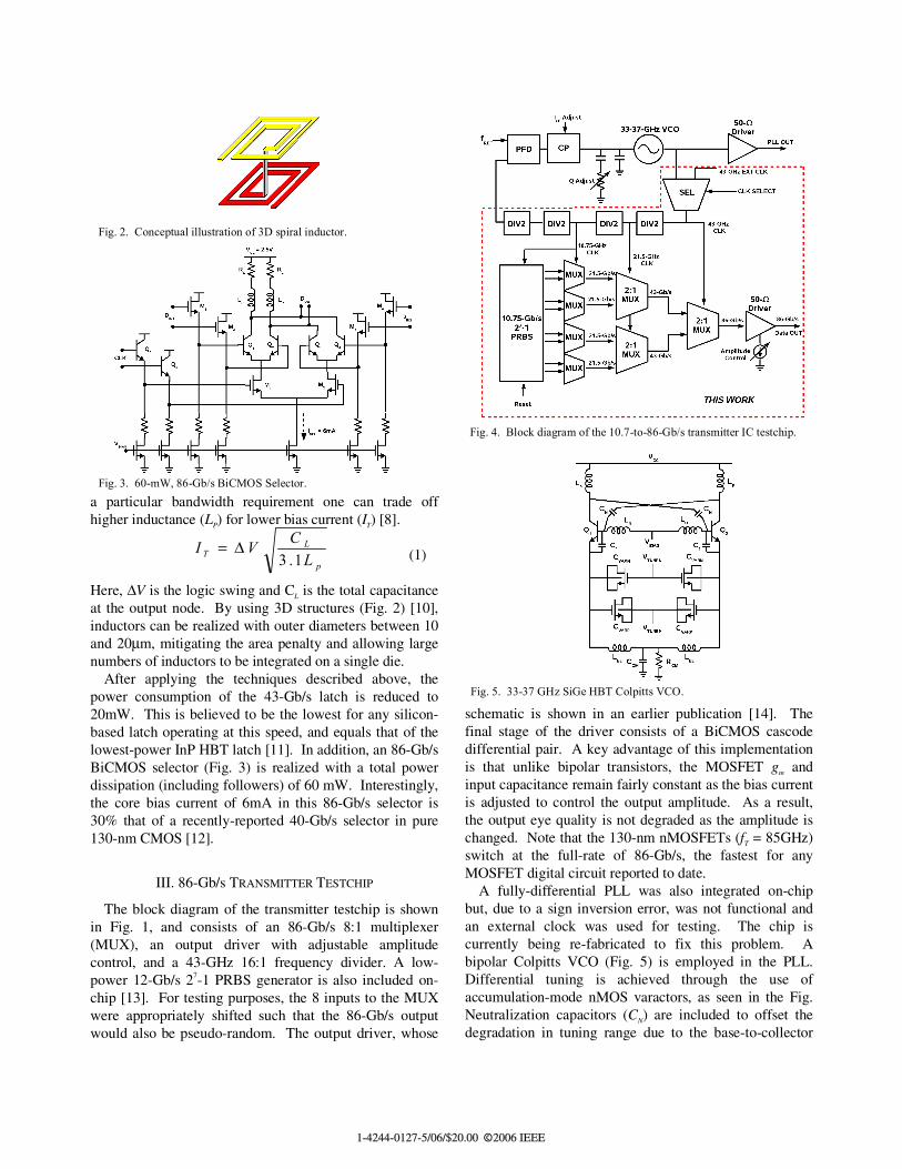
Here, ∆V is the logic swing and CL is the total capacitance at the output node. By using 3D structures (Fig. 2) [10], inductors can be realized with outer diameters between 10 and 20µm, mitigating the area penalty and allowing large numbers of inductors to be integrated on a single die.
After applying the techniques described above, the power consumption of the 43-Gb/s latch is reduced to 20mW. This is believed to be the lowest for any silicon-based latch operating at this speed, and equals that of the lowest-power InP HBT latch [11]. In addition, an 86-Gb/s BiCMOS selector (Fig. 3) is realized with a total power dissipation (including followers) of 60 mW. Interestingly, the core bias current of 6mA in this 86-Gb/s selector is 30% that of a recently-reported 40-Gb/s selector in pure 130-nm CMOS [12].
III. 86-Gb/s TRANSMITTER TESTCHIP
The block diagram of the transmitter testchip is shown in Fig. 1, and consists of an 86-Gb/s 8:1 multiplexer (MUX), an output driver with adjustable amplitude control, and a 43-GHz 16:1 frequency divider. A low-power 12-Gb/s 27-1 PRBS generator is also included on-chip [13]. For testing purposes, the 8 inputs to the MUX were appropriately shifted such that the 86-Gb/s output would also be pseudo-random. The output driver, whose
schematic is shown in an earlier publication [14]. The final stage of the driver consists of a BiCMOS cascode differential pair. A key advantage of this implementation is that unlike bipolar transistors, the MOSFET gm and input capacitance remain fairly constant as the bias current is adjusted to control the output amplitude. As a result, the output eye quality is not degraded as the amplitude is changed. Note that the 130-nm nMOSFETs (fT = 85GHz) switch at the full-rate of 86-Gb/s, the fastest for any MOSFET digital circuit reported to date.
A fully-differential PLL was also integrated on-chip but, due to a sign inversion error, was not functional and an external clock was used for testing. The chip is currently being re-fabricated to fix this problem. A bipolar Colpitts VCO (Fig. 5) is employed in the PLL. Differential tuning is achieved through the use of accumulation-mode nMOS varactors, as seen in the Fig. Neutralization capacitors (CN) are included to offset the degradation in tuning range due to the base-to-collector
Fig. 2. Conceptual illustration of 3D spiral inductor.
Fig. 4. Block diagram of the 10.7-to-86-Gb/s transmitter IC testchip.
p
LT L
CVI1.3
∆=
Fig. 3. 60-mW, 86-Gb/s BiCMOS Selector.
Fig. 5. 33-37 GHz SiGe HBT Colpitts VCO.
©1-4244-0127-5/06/$20.00 2006 IEEE
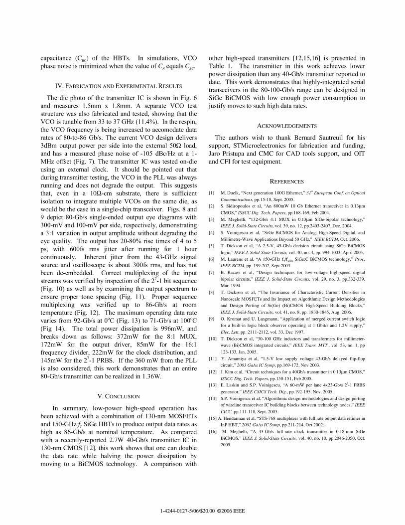
capacitance (CBC) of the HBTs. In simulations, VCO phase noise is minimized when the value of CN equals CBC.
IV. FABRICATION AND EXPERIMENTAL RESULTS
The die photo of the transmitter IC is shown in Fig. 6 and measures 1.5mm x 1.8mm. A separate VCO test structure was also fabricated and tested, showing that the VCO is tunable from 33 to 37 GHz (11.4%). In the respin, the VCO frequency is being increased to accomodate data rates of 80-to-86 Gb/s. The current VCO design delivers 3dBm output power per side into the external 50Ω load, and has a measured phase noise of -105 dBc/Hz at a 1-MHz offset (Fig. 7). The transmitter IC was tested on-die using an external clock. It should be pointed out that during transmitter testing, the VCO in the PLL was always running and does not degrade the output. This suggests that, even in a 10Ω-cm substrate, there is sufficient isolation to integrate multiple VCOs on the same die, as would be the case in a single-chip transceiver. Figs. 8 and 9 depict 80-Gb/s single-ended output eye diagrams with 300-mV and 100-mV per side, respectively, demonstrating a 3:1 variation in output amplitude without degrading the eye quality. The output has 20-80% rise times of 4 to 5 ps, with 600fs rms jitter after running for 1 hour continuously. Inherent jitter from the 43-GHz signal source and oscilloscope is about 300fs rms, and has not been de-embedded. Correct multiplexing of the input streams was verified by inspection of the 27-1 bit sequence (Fig. 10) as well as by examining the output spectrum to ensure proper tone spacing (Fig. 11). Proper sequence multiplexing was verified up to 86-Gb/s at room temperature (Fig. 12). The maximum operating data rate varies from 92-Gb/s at 0oC (Fig. 13) to 71-Gb/s at 100oC (Fig 14). The total power dissipation is 996mW, and breaks down as follows: 372mW for the 8:1 MUX, 172mW for the output driver, 85mW for the 16:1 frequency divider, 222mW for the clock distribution, and 145mW for the 27-1 PRBS. If the 360 mW from the PLL is also considered, this work demonstrates that an entire 80-Gb/s transmitter can be realized in 1.36W.
V. CONCLUSION
In summary, low-power high-speed operation has been achieved with a combination of 130-nm MOSFETs and 150-GHz fT SiGe HBTs to produce output data rates as high as 86-Gb/s at nominal temperature. As compared with a recently-reported 2.7W 40-Gb/s transmitter IC in 130-nm CMOS [12], this work shows that one can double the data rate while halving the power dissipation by moving to a BiCMOS technology. A comparison with
other high-speed transmitters [12,15,16] is presented in Table 1. The transmitter in this work achieves lower power dissipation than any 40-Gb/s transmitter reported to date. This work demonstrates that highly-integrated serial transceivers in the 80-100-Gb/s range can be designed in SiGe BiCMOS with low enough power consumption to justify moves to such high data rates.
ACKNOWLEDGEMENTS
The authors wish to thank Bernard Sautreuil for his support, STMicroelectronics for fabrication and funding, Jaro Pristupa and CMC for CAD tools support, and OIT and CFI for test equipment.
REFERENCES
[1] M. Duelk, “Next generation 100G Ethernet,” 31st European Conf. on Optical
Communications, pp.15-18, Sept. 2005.
[2] S. Sidiropoulos et al, “An 800mW 10 Gb Ethernet transceiver in 0.13µm
CMOS,” ISSCC Dig. Tech. Papers, pp.168-169, Feb 2004.
[3] M. Meghelli, “132-Gb/s 4:1 MUX in 0.13µm SiGe-bipolar technology,”
IEEE J. Solid-State Circuits, vol. 39, no. 12, pp.2403-2407, Dec. 2004.
[4] S. Voinigescu et al, “SiGe BiCMOS for Analog, High-Speed Digital, and Millimetre-Wave Applications Beyond 50 GHz,” IEEE BCTM, Oct. 2006.
[5] T. Dickson et al, “A 2.5-V, 45-Gb/s decision circuit using SiGe BiCMOS
logic,” IEEE J. Solid-State Circuits, vol. 40, no. 4, pp. 994-1003, April 2005.
[6] M. Laurens et al, “A 150-GHz fT/fMAX SiGe:C BiCMOS technology,” Proc.
IEEE BCTM, pp. 199-202, Sept 2003.
[7] B. Razavi et al, “Design techniques for low-voltage high-speed digital
bipolar circuits,” IEEE J. Solid-State Circuits, vol. 29, no. 3, pp.332-339,
Mar. 1994.
[8] T. Dickson et al, “The Invariance of Characteristic Current Densities in Nanoscale MOSFETs and Its Impact on Algorithmic Design Methodologies and Design Porting of Si(Ge) (Bi)CMOS High-Speed Building Blocks,”
IEEE J. Solid-State Circuits, vol. 41, no. 8, pp. 1830-1845, Aug. 2006.
[9] O. Kromat and U. Langmann, “Application of merged current switch logic
for a built-in logic block observer operating at 1 Gbit/s and 1.2V supply,”
Elec. Lett, pp. 2111-2112, vol. 33, Dec 1997.
[10] T. Dickson et al, “30-100 GHz inductors and transformers for millimeter-
wave (Bi)CMOS integrated circuits,” IEEE Trans. MTT., vol. 53, no. 1, pp
123-133, Jan. 2005.
[11] Y. Amamiya et al, “1.5-V low supply voltage 43-Gb/s delayed flip-flop
circuit,” 2003 GaAs IC Symp, pp.169-172, Nov 2003.
[12] J. Kim et al, “Circuit techniques for a 40Gb/s transmitter in 0.13µm CMOS,”
ISSCC Dig. Tech. Papers, pp.150-151, Feb 2005.
[13] E. Laskin and S.P. Voinigescu, “A 60-mW per lane 4x23-Gb/s 27-1 PRBS
generator,” IEEE CSICS Tech. Dig., pp.192-195, Nov. 2005.
[14] S.P. Voinigescu et al, “Algorithmic design methodologies and design porting
of wireline transceiver IC building blocks between technology nodes,” IEEE
CICC, pp.111-118, Sept. 2005.
[15] A. Hendarman et al, “STS-768 multiplexer with full rate output data retimer in
InP HBT,” 2002 GaAs IC Symp, pp.211-214, Oct 2002.
[16] M. Meghelli, “A 43-Gb/s full-rate clock transmitter in 0.18-mm SiGe
BiCMOS,” IEEE J. Solid-State Circuits, vol. 40, no. 10, pp.2046-2050, Oct.
2005.
©1-4244-0127-5/06/$20.00 2006 IEEE

Fig. 6. Die photo of 86-Gb/s transmitter IC testchip.
Fig. 7. Measured VCO spectrum showing phase noise of -105dBc/Hz @ 1-MHz offset.
Fig. 8. Measured 80-Gb/s single-ended output eye diagram with 300mV per side swing.
Fig. 9. Measured 80-Gb/s single-ended output eye diagram with 100mV per side swing.
Fig. 10. Measured 80-Gb/s 80-Gb/s output bit sequence.
Fig. 11. Measured output spectrum demonstrating correct PRBS multiplexing.
Fig. 12. Measured output eye at maximum output data rate of 86-Gb/s.
Fig. 13. Measured 71-Gb/s output eye diagram at 100oC.
Fig. 14. Measured 92-Gb/s output eye diagram at 0oC.
Technology fT/fMAX Data rate Supply Voltage
PDISS Ref.
130-nm CMOS ~85/90 GHz 40 (half-rate) 1.5 V 2.7 W [12] InP HBT 150/150 GHz 43 (full-rate) -3.6/-5.2 V 3.6 W [15] 180-nm SiGe BiCMOS HBT: 120/100 GHz 43 (half-rate) -3.6 V 1.6 W [16] 180-nm SiGe BiCMOS HBT: 120/100 GHz 43 (full-rate) -3.6 V 2.3 W [16] 130-nm SiGe BiCMOS MOS: 85/90 GHz
HBT: 150/160 GHz 86 (half-rate) 2.5 V 1.36 W This Work
Table 1. Comparison of high-speed transmitter power dissipation in various technologies.
©1-4244-0127-5/06/$20.00 2006 IEEE