Low noise, Chopper Stabilized Operational Amplifiier · load than with a 10kΩ load.) If the amp is...
16
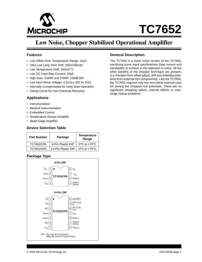
2002 Microchip Technology Inc. DS21464B-page 1 Features • Low Offset Over Temperature Range: 10µV • Ultra Low Long Term Drift: 150nV/Month • Low Temperature Drift: 100nV/°C • Low DC Input Bias Current: 15pA • High Gain, CMRR and PSRR: 110dB Min • Low Input Noise Voltage: 0.2µVp-p (DC to 1Hz) • Internally Compensated for Unity Gain Operation • Clamp Circuit for Fast Overload Recovery Applications • Instrumentation • Medical Instrumentation • Embedded Control • Temperature Sensor Amplifier • Strain Gage Amplifier Device Selection Table Package Type General Description The TC7652 is a lower noise version of the TC7650, sacrificing some input specifications (bias current and bandwidth) to achieve a 10x reduction in noise. All the other benefits of the chopper technique are present, (i.e, freedom from offset adjust, drift and reliability prob- lems from external trim components). Like the TC7650, the TC7652 requires only two noncritical external caps for storing the chopped null potentials. There are no significant chopping spikes, internal effects or over- range lockup problems. Part Number Package Temperature Range TC7652CPA 8-Pin Plastic DIP 0°C to +70°C TC7652CPD 14-Pin Plastic DIP 0°C to +70°C 1 2 3 4 8 7 6 5 C A Output TC7652CPA -Input +Input V SS V DD C B Output Clamp V SS V DD 1 2 3 4 5 6 7 14 13 12 11 10 9 8 NC NC = No Internal Connection (May Be Used As Input Guard) INT/EXT EXT CLK In INT CLK Out Output Output Clamp C RETN -Input +Input NC TC7652CPD C B C A 8-Pin DIP 14-Pin DIP TC7652 Low Noise, Chopper Stabilized Operational Amplifier
Transcript of Low noise, Chopper Stabilized Operational Amplifiier · load than with a 10kΩ load.) If the amp is...
2002 Microchip Technology Inc. DS21464B-page 1
Features
• Low Offset Over Temperature Range: 10µV
• Ultra Low Long Term Drift: 150nV/Month
• Low Temperature Drift: 100nV/°C
• Low DC Input Bias Current: 15pA
• High Gain, CMRR and PSRR: 110dB Min
• Low Input Noise Voltage: 0.2µVp-p (DC to 1Hz)
• Internally Compensated for Unity Gain Operation
• Clamp Circuit for Fast Overload Recovery
Applications
• Instrumentation
• Medical Instrumentation
• Embedded Control
• Temperature Sensor Amplifier
• Strain Gage Amplifier
Device Selection Table
Package Type
General Description
The TC7652 is a lower noise version of the TC7650,sacrificing some input specifications (bias current andbandwidth) to achieve a 10x reduction in noise. All theother benefits of the chopper technique are present,(i.e, freedom from offset adjust, drift and reliability prob-lems from external trim components). Like the TC7650,the TC7652 requires only two noncritical external capsfor storing the chopped null potentials. There are nosignificant chopping spikes, internal effects or over-range lockup problems.
Part Number PackageTemperature
Range
TC7652CPA 8-Pin Plastic DIP 0°C to +70°C
TC7652CPD 14-Pin Plastic DIP 0°C to +70°C
1
2
3
4
8
7
6
5
CA
OutputTC7652CPA
-Input
+Input
VSS
VDD
CB
Output Clamp
VSS
VDD
1
2
3
4
5
6
7
14
13
12
11
10
9
8
NC
NC = No Internal Connection (May Be Used As Input Guard)
INT/EXT
EXT CLKInINT CLKOut
Output
OutputClamp
CRETN
-Input
+Input
NC
TC7652CPD
CB
CA
8-Pin DIP
14-Pin DIP
TC7652Low Noise, Chopper Stabilized Operational Amplifier

TC7652
DS21464B-page 2 2002 Microchip Technology Inc.
Functional Block Diagram
TC7652
NULL
NULL
Output
BB
A
CA
CB
CRETN (1)
NULLAmplifier
MainAmplifier
Output ClampCircuit
IntermodComparator
Oscillator
BA
INT/EXTEXT CLK INCLK OUT
14-Pin DIP Only
B A
Inputs
Output Clamp(Not On "Z" Pinout)
NOTE 1: For 8-pin DIP connect to VSS, or to CRET on "Z" pinout.
VSS

2002 Microchip Technology Inc. DS21464B-page 3
TC7652
1.0 ELECTRICALCHARACTERISTICS
ABSOLUTE MAXIMUM RATINGS*
Total Supply Voltage (VDD to VSS) .......................+18V
Input Voltage .................... (VDD +0.3V) to (VSS – 0.3V)
Voltage on Oscillator Control Pins...............VDD to VSS
Duration of Output Short Circuit ..................... Indefinite
Current Into Any Pin............................................ 10mA
While Operating (Note 1)............................100µA
Package Power Dissipation (TA < 70°C)
8-Pin Plastic DIP....................................... 730mW
14-Pin Plastic DIP..................................... 800mW
Storage Temperature Range.............. -65°C to +150°C
Operating Temperature Range
C Device .......................................... 0°C to +70°C
I Device ......................................... -25°C to +85°C
*Stresses above those listed under “Absolute MaximumRatings” may cause permanent damage to the device.These are stress ratings only and functional operation of thedevice at these or any other conditions above those indi-cated in the operation sections of the specifications is notimplied. Exposure to Absolute Maximum Rating conditionsfor extended periods my affect device reliability.
TC7652 ELECTRICAL SPECIFICATIONS
Electrical Characteristics: VDD = +5V, VSS = -5V, TA = +25°C, unless otherwise indicated.
Symbol Parameter Min Typ Max Units Test Conditions
VOS Input Offset Voltage — ±2 ±5 µV TA = +25°C
TCVOS Average Temperature Co-efficient ofInput Offset Voltage
— 0.01 0.05 µV/°C 0°C < TA < +70°C
VOS/DT Offset Voltage vs Time — 150 — nV/mo
IBIAS Input Bias Current (CLK On) ———
30100250
100—
1000
pA TA = +25°C0°C < TA < +70°C-25°C < TA < +85°C
IBIAS Input Bias Current (CLK Off) ———
1535100
30—
1000
pA TA = +25°C0°C < TA < +70°C-25°C < TA < +85°C
IOS Input Offset Current — 25 150 pA
RIN Input Resistance — 1012 — Ω
OL Large Signal Voltage Gain 120 150 — dB RL = 10kΩ, VOUT = ±4V
VOUT Output Voltage Swing (Note 2) ±4.7—
±4.85±4.95
——
V RL = 10kΩRL = 100kΩ
CMVR Common Mode Voltage Range -4.3 — +3.5 V
MRR Common Mode Rejection Ratio 120 140 — dB CMVR = -4.3V to +3.5V
PSRR Power Supply 120 140 — dB ±3V to ±8V
eN Input Noise Voltage ——
0.20.7
1.55
µVP-PµVP-P
RS = 100Ω, DC to 1HzDC to 10Hz
IN Input Noise Current — 0.01 — pA/√Hz
f = 10Hz
GBW Unity Gain Bandwidth — 0.4 — MHz
SR Slew Rate — 1 — V/µsec CL = 50pF, RL = 10kΩ
Overshoot — 15 — %
VDD, VSS Operating Supply Range 5 — 16 V
Note 1: Limiting input current to 100µA is recommended to avoid latch-up problems. Typically 1mA is safe however, this is notguaranteed.
2: Output clamp not connected. See typical characteristics curves for output swing versus clamp current characteristics.3: See “Output Clamp” under detailed description.

TC7652
DS21464B-page 4 2002 Microchip Technology Inc.
IS Supply Current — 1 3 mA No Load
fCH Internal Chopping Frequency 100 275 — Hz Pins 12 – 14 Open (DIP)
Clamp ON Current (Note 3) 25 100 — µA RL = 100kΩ
Clamp OFF Current (Note 3) — 1 — pA -4V ≤ VOUT < +10V
TC7652 ELECTRICAL SPECIFICATIONS (CONTINUED)
Electrical Characteristics: VDD = +5V, VSS = -5V, TA = +25°C, unless otherwise indicated.
Symbol Parameter Min Typ Max Units Test Conditions
Note 1: Limiting input current to 100µA is recommended to avoid latch-up problems. Typically 1mA is safe however, this is notguaranteed.
2: Output clamp not connected. See typical characteristics curves for output swing versus clamp current characteristics.3: See “Output Clamp” under detailed description.

2002 Microchip Technology Inc. DS21464B-page 5
TC7652
2.0 PIN DESCRIPTIONS
The descriptions of the pins are listed in Table 2-1.
TABLE 2-1: PIN FUNCTION TABLE
Pin NumberSymbol Description
8-pin DIP 14-pin DIP
1,8 2,1 CA, CB Nulling capacitor pins
2 4 -INPUT Inverting Input
3 5 +INPUT Non-inverting Input
4 7 VSS Negative Power Supply
5 9 OUTPUTCLAMP
Output Voltage Clamp
6 10 OUTPUT Output
7 11 VDD Positive Power Supply
— 3,6 NC No internal connection
— 8 CRETN Capacitor current return pin
— 12 INT CLK OUT Internal Clock Output
— 13 EXT CLK IN External Clock Input
— 14 INT/EXT Select Internal or External Clock
TC7652
DS21464B-page 6 2002 Microchip Technology Inc.
3.0 DETAILED DESCRIPTION
3.1 Capacitor Connection
Connect the null storage capacitors to the CA and CBpins with a common connection to the CRET pin (14-pinTC7652) or to VSS (8-pin TC7652). When connecting toVSS, avoid injecting load current IR drops into thecapacitive circuitry by making this connection directlyvia a separate wire or PC trace.
3.2 Output Clamp
In chopper stabilized amplifiers, the output clamp pinreduces overload recovery time. When a connection ismade to the inverting input pin (summing junction), acurrent path is created between that point and the out-put pin, just before the device output saturates. Thisprevents uncontrolled differential input voltages andcharge build-up on correction storage capacitors. Out-put swing is reduced.
3.3 Clock
The TC7652 has a 550Hz internal oscillator, which isdivided by two before clocking the input chopperswitches. The 275Hz chopping frequency is availableat INT CLK OUT (Pin 12) on 14-pin devices. In normaloperation, INT/EXT (Pin 14), which has an internal pull-up, can be left open.
An external clock can also be used. To disable theinternal clock and use an external one, the INT/EXT pinmust be tied to VSS. The external clock signal is thenapplied to the EXT CLK IN input (Pin 13). An internaldivide-by-two provides a 50% switching duty cycle. Thecapacitors are only charged when EXT CLK IN is high,so a 50% to 80% positive duty cycle is recommendedfor higher clock frequencies. The external clock canswing between VDD and VSS, with the logic thresholdabout 2.5V below VDD.
The output of the internal oscillator, before the divide-by-two circuit, is available at EXT CLK IN when INT/EXT is high or unconnected. This output can serve asthe clock input for a second TC7652 (operating in amaster/slave mode), so that both op amps will clock atthe same frequency. This prevents clock intermodula-tion effects when two TC7652's are used in a differen-tial amplifier configuration.
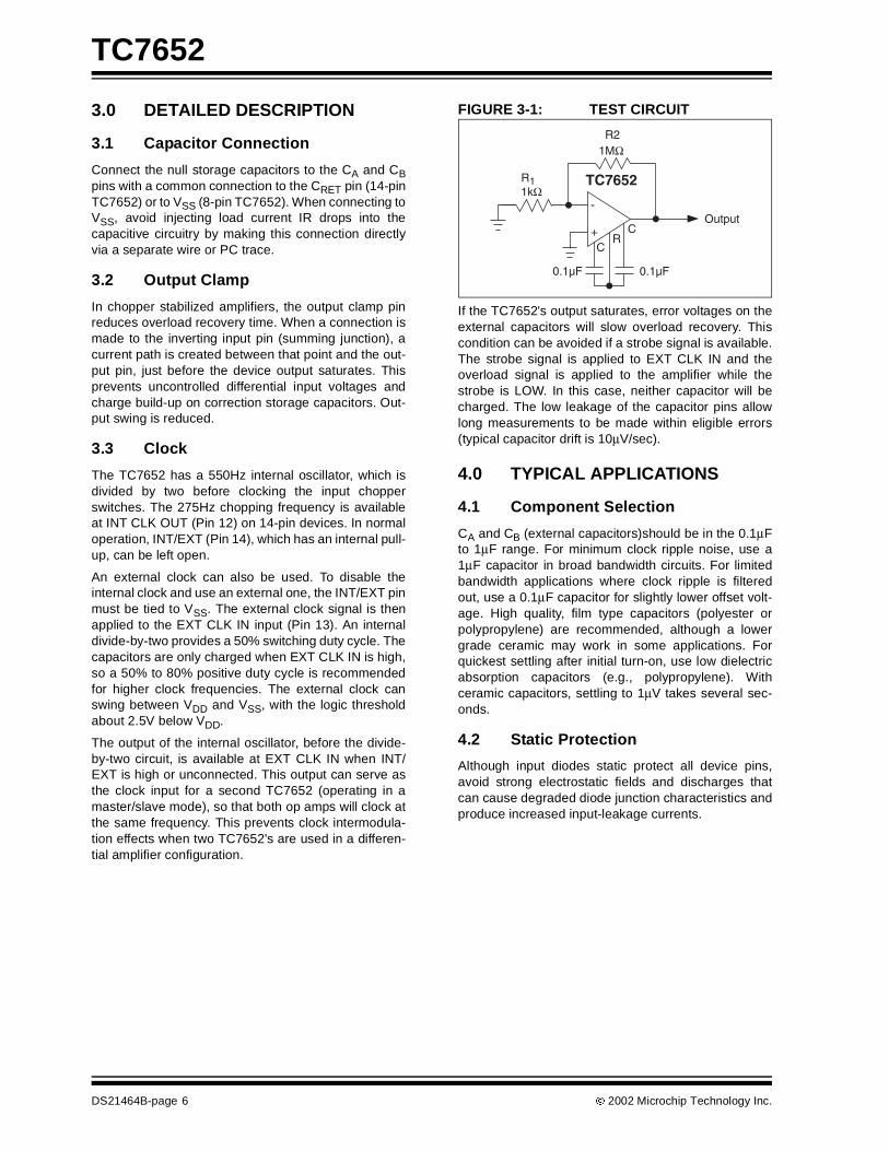
FIGURE 3-1: TEST CIRCUIT
If the TC7652's output saturates, error voltages on theexternal capacitors will slow overload recovery. Thiscondition can be avoided if a strobe signal is available.The strobe signal is applied to EXT CLK IN and theoverload signal is applied to the amplifier while thestrobe is LOW. In this case, neither capacitor will becharged. The low leakage of the capacitor pins allowlong measurements to be made within eligible errors(typical capacitor drift is 10µV/sec).
4.0 TYPICAL APPLICATIONS
4.1 Component Selection
CA and CB (external capacitors)should be in the 0.1µFto 1µF range. For minimum clock ripple noise, use a1µF capacitor in broad bandwidth circuits. For limitedbandwidth applications where clock ripple is filteredout, use a 0.1µF capacitor for slightly lower offset volt-age. High quality, film type capacitors (polyester orpolypropylene) are recommended, although a lowergrade ceramic may work in some applications. Forquickest settling after initial turn-on, use low dielectricabsorption capacitors (e.g., polypropylene). Withceramic capacitors, settling to 1µV takes several sec-onds.
4.2 Static Protection
Although input diodes static protect all device pins,avoid strong electrostatic fields and discharges thatcan cause degraded diode junction characteristics andproduce increased input-leakage currents.
+
-
Output
R2
R1
0.1µF 0.1µF
TC7652
CR
C
1kΩ
1MΩ

2002 Microchip Technology Inc. DS21464B-page 7
TC7652
4.3 Output Stage/Load Driving
The output circuit is high impedance (about 18kΩ).With lesser loads, the chopper amplifier behavessomewhat like a transconductance amplifier with anopen-loop gain proportional to load resistance. (Forexample, the open-loop gain is 17dB lower with a 1kΩ.load than with a 10kΩ load.) If the amp is used only forDC, the DC gain is typically greater than 120dB (even
with a 1kΩ load), and this lower gain is inconsequential.For wide band, the best frequency response occurswith a load resistor of at least 10kΩ. This produces a6dB/octave response from 0.1Hz to 2MHz, with phaseshifts of less than 2 degrees in the transition region,where the main amplifier takes over from the null ampli-fier.
FIGURE 4-1: CONNECTION OF INPUT GUARDS
4.4 Thermoelectric Effects
The thermoelectric (Seebeck) effects in thermocouplejunctions of dissimilar metals, alloys, silicon, etc. limitultra high precision DC amplifiers. Unless all junctionsare at the same temperature, thermoelectric voltagesaround 0.1µV/°C (up to tens of µV/°C for some materi-als) are generated. To realize the low offset voltages ofthe chopper, avoid temperature gradients. Enclosecomponents to eliminate air movement, especially frompower dissipating elements in the system. Where pos-sible, use low thermoelectric co-efficient connections.Keep power supply voltages and power dissipation to aminimum. Use high impedance loads and seek maxi-mum separation from surrounding heat disipating ele-ments.
4.5 Guarding
To benefit from TC7652 low input currents, take careassembling printed circuit boards. Clean boards withalcohol or TCE and blow dry with compressed air. Toprevent contamination, coat boards with epoxy or sili-cone rubber.
Even if boards are cleaned and coated, leakage cur-rents may occur because input pins are next to pins atsupply potentials. To reduce this leakage, use guardingto lower the voltage difference between the inputs andadjacent metal runs. The guard (a conductive ring sur-rounding inputs) is connected to a low impedance pointat about the same voltage as inputs. The guardabsorbs leakage currents from high voltage pins.
The 14-pin dual-in-line arrangement simplifies guard-ing. Like the LM108 pin configuration (but unlike the101A and 741), pins next to inputs are not used.
Input
+Output
R2R1
Inverting Amplifier
Input+
Output
Follower
Input
+Output
R2
R1
Noninverting Amplifier
TC7652 TC7652
TC7652-
--

TC7652
DS21464B-page 8 2002 Microchip Technology Inc.
4.6 Pin Compatibility
Where possible, the 8-pin device pinout conforms tosuch industry standards as the LM101 and LM741. Nullstoring external capacitors connect to Pins 1 and 8,which are usually for offset null or compensation capac-itors. Output clamp (Pin 5) is similarly used. For OP05and OP07 devices, replacement of the offset nullpotentiometer (connected between Pins 1 and 8 andVDD by two capacitors from those pins to VSS) providescompatibility. Replacing the compensation capacitorbetween Pins 1 and 8 by two capacitors to VSS isrequired. The same operation (with the removal of anyconnection to Pin 5) works for LM101, µA748 and sim-ilar parts.
Because NC pins provide guarding between input andother pins, the 14-pin device pinout conforms closely tothe LM108. Because this device does not use any extrapins and does not provide offset nulling (but requires acompensation capacitor), some layout changes arenecessary to convert to the TC7652.
4.7 Some Applications
Figures 4-2 and 4-3 show basic inverting and nonin-verting amplifier circuits using the output clamping cir-cuit to enhance overload recovery performance. Theonly limitations on replacing other op amps with theTC7652 are supply voltage (±8V maximum) and outputdrive capability (10kΩ load for full swing). Overcomethese limitations with a booster circuit (Figure 4-4) tocombine output capabilities of the LM741 (or otherstandard device) with input capabilities of the TC7652.These two form a composite device, therefore, whenadding the feedback network, the monitor loop gainsstability.
FIGURE 4-2: NONINVERTINGAMPLIFIER WITHOPTIONAL CLAMP
FIGURE 4-3: INVERTING AMPLIFIERWITH OPTIONAL CLAMP
FIGURE 4-4: USING 741 TO BOOSTOUTPUT DRIVECAPABILITY
Figure 4-5 shows the clamp circuit of a zero offset com-parator. Because the clamp circuit requires the invert-ing input to follow the input signal, problems with achopper stabilized op amp are avoided. The thresholdinput must tolerate the output clamp current ≈VIN/Rwithout disrupting other parts of the system.
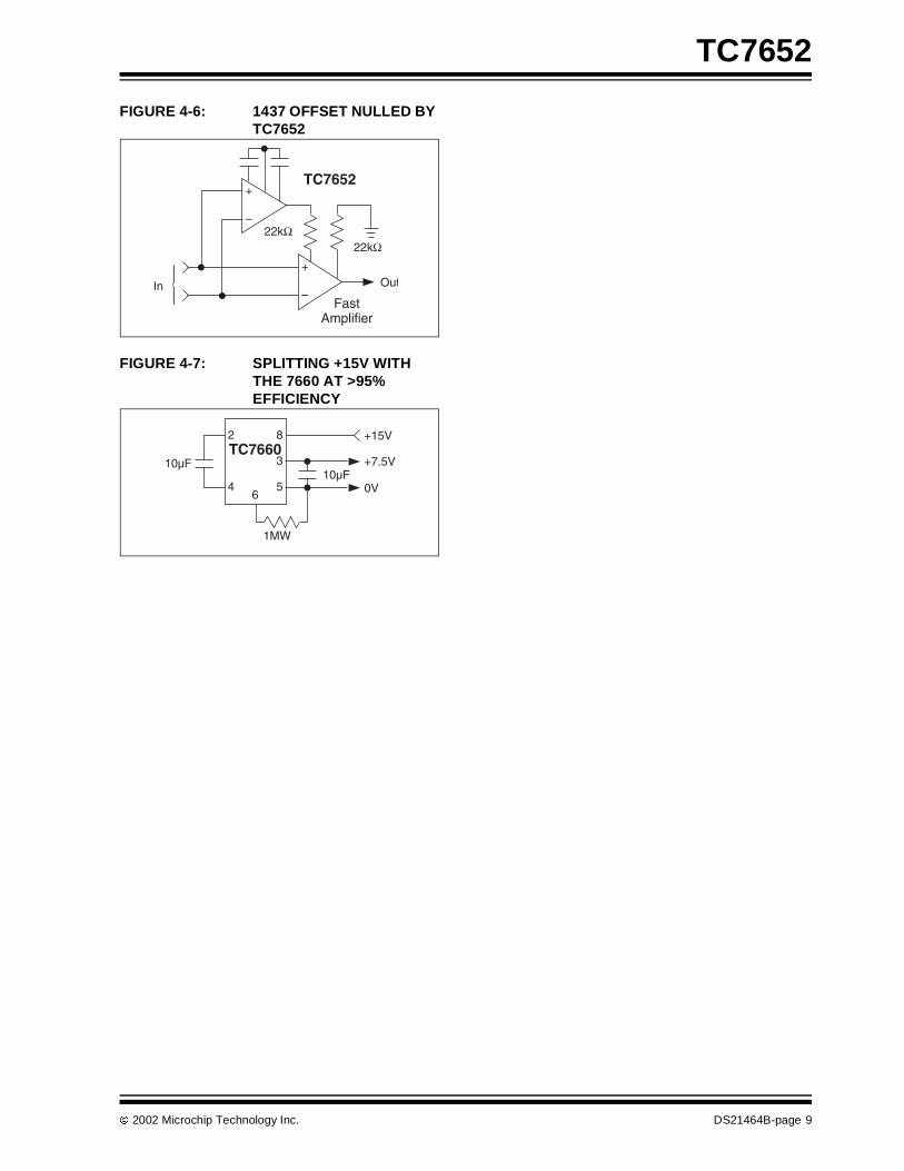
Figure 4-6 shows how the TC7652 can offset null highslew rate and wideband amplifiers.
Mixing the TC7652 with circuits operating at ±15Vrequires a lower supply voltage divider with the TC7660voltage converter circuit operated "backwards." Figure4-7 shows an approximate connection.
FIGURE 4-5: LOW OFFSETCOMPARATOR
TC7652+
–Output
Clamp
Input
0.1µF
R2
R1R3
0.1µF
+
–
OutputInput
R2
R1 Clamp
0.1µF 0.1µF
TC7652
+
–+
–
+15V
-15V
-7.5V
0.1µF
InOut
-7.5V
0.1µF
10kΩ
TC7652
741
TC7652+
–VOUT
Clamp
VIN
0.1µF 0.1µF
200kΩ to 2mΩVTH
2002 Microchip Technology Inc. DS21464B-page 9
TC7652
FIGURE 4-6: 1437 OFFSET NULLED BYTC7652
FIGURE 4-7: SPLITTING +15V WITHTHE 7660 AT >95%EFFICIENCY
+
–
TC7652
OutIn
+
–
22kΩ22kΩ
FastAmplifier
2
4 5
3
8TC7660
6
10µF
1MW
10µF
+15V
+7.5V
0V
TC7652
DS21464B-page 10 2002 Microchip Technology Inc.
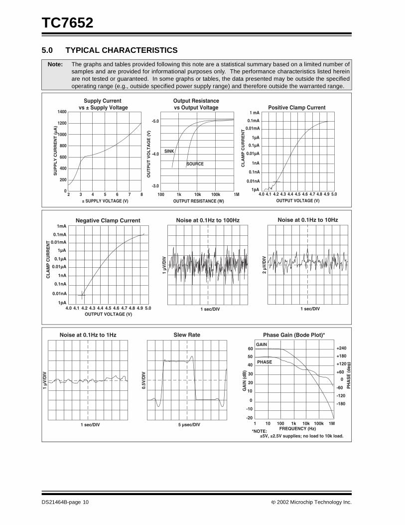
5.0 TYPICAL CHARACTERISTICS
Note: The graphs and tables provided following this note are a statistical summary based on a limited number ofsamples and are provided for informational purposes only. The performance characteristics listed hereinare not tested or guaranteed. In some graphs or tables, the data presented may be outside the specifiedoperating range (e.g., outside specified power supply range) and therefore outside the warranted range.
2 3 4 5 6 7 8± SUPPLY VOLTAGE (V)
1400
1200
1000
800
600
400
200
0
SU
PP
LY
CU
RR
EN
T (
µA
)
Supply Current vs ± Supply Voltage
OUTPUT VOLTAGE (V)4.0 4.1 4.2 4.3 4.4 4.5 4.6 4.7 4.8 4.9 5.0
1 mA
0.1mA
0.01mA
1µA
0.1µA
0.01µA
1nA
0.1nA
0.01nA
1pA
CL
AM
P C
UR
RE
NT
Positive Clamp Current
SOURCE
SINK
Output Resistancevs Output Voltage
100OUTPUT RESISTANCE (W)
-3.0
OU
TP
UT
VO
LT
AG
E (
V)
1k 10k 100k 1M
-5.0
-4.0
1 sec/DIV
2 µV
/DIV
Noise at 0.1Hz to 10Hz
OUTPUT VOLTAGE (V)4.0 4.1 4.2 4.3 4.4 4.5 4.6 4.7 4.8 4.9 5.0
1mA
0.1mA
0.01mA
1µA
0.1µA
0.01µA
1nA
0.1nA
0.01nA
1pA
CLA
MP
CU
RR
EN
T
Negative Clamp Current
1 sec/DIV
1 µV
/DIV
Noise at 0.1Hz to 100Hz
1 sec/DIV
1 µV
/DIV
Noise at 0.1Hz to 1Hz
1 10 100 1k 10k 100k 1MFREQUENCY (Hz)
GAIN
-20
-10
0
10
20
30
40
60
GA
IN (d
B)
Phase Gain (Bode Plot)*
*NOTE:±5V, ±2.5V supplies; no load to 10k load.
-180
-120
-60
+60
+120
+180
+240
50
PH
AS
E (d
eg)
0
5 µsec/DIV
0.5V
/DIV
Slew Rate
PHASE

2002 Microchip Technology Inc. DS21464B-page 11
TC7652
-6 -4 -2 0 2 4
COMMON MODE VOLTAGE (V)
Input Offset Voltage vs Common Mode Voltage4.0
3.5
3.0
2.5
2.0
1.5
1.0
0.5
INP
UT
OFF
SE
T V
OLT
AG
E (µ
V)

TC7652
DS21464B-page 12 2002 Microchip Technology Inc.
6.0 PACKAGING INFORMATION
6.1 Package Marking Information
Package marking information not available at this time.
6.2 Package Dimensions
3˚MIN.
PIN 1
.260 (6.60)
.240 (6.10)
.045 (1.14)
.030 (0.76).070 (1.78).040 (1.02)
.400 (10.16).348 (8.84)
.200 (5.08)
.140 (3.56)
.150 (3.81)
.115 (2.92)
.110 (2.79)
.090 (2.29).022 (0.56).015 (0.38)
.040 (1.02)
.020 (0.51) .015 (0.38).008 (0.20)
.310 (7.87)
.290 (7.37)
.400 (10.16).310 (7.87)
8-Pin Plastic DIP
Dimensions: inches (mm)
.260 (6.60)
.240 (6.10)
.770 (19.56)
.745 (18.92)
.310 (7.87)
.290 (7.37)
.040 (1.02)
.020 (0.51)
.070 (1.78)
.045 (1.14).022 (0.56).015 (0.38)
.110 (2.79)
.090 (2.29)
.200 (5.08)
.140 (3.56)
.150 (3.81)
.115 (2.92)
PIN 1
14-Pin PDIP (Narrow)
.015 (0.38)
.008 (0.20) 3˚MIN.
.400 (10.16).310 (7.87)
Dimensions: inches (mm)

2002 Microchip Technology Inc. DS21464B-page 13
TC7652
SALES AND SUPPORT
Data SheetsProducts supported by a preliminary Data Sheet may have an errata sheet describing minor operational differences and recom-mended workarounds. To determine if an errata sheet exists for a particular device, please contact one of the following:
1. Your local Microchip sales office2. The Microchip Corporate Literature Center U.S. FAX: (480) 792-72773. The Microchip Worldwide Site (www.microchip.com)
Please specify which device, revision of silicon and Data Sheet (include Literature #) you are using.
New Customer Notification SystemRegister on our web site (www.microchip.com/cn) to receive the most current information on our products.

TC7652
DS21464B-page 14 2002 Microchip Technology Inc.
NOTES:
2002 Microchip Technology Inc. DS21464B - page 15
Information contained in this publication regarding deviceapplications and the like is intended through suggestion onlyand may be superseded by updates. It is your responsibility toensure that your application meets with your specifications.No representation or warranty is given and no liability isassumed by Microchip Technology Incorporated with respectto the accuracy or use of such information, or infringement ofpatents or other intellectual property rights arising from suchuse or otherwise. Use of Microchip’s products as critical com-ponents in life support systems is not authorized except withexpress written approval by Microchip. No licenses are con-veyed, implicitly or otherwise, under any intellectual propertyrights.
Trademarks
The Microchip name and logo, the Microchip logo, FilterLab,KEELOQ, microID, MPLAB, PIC, PICmicro, PICMASTER,PICSTART, PRO MATE, SEEVAL and The Embedded ControlSolutions Company are registered trademarks of Microchip Tech-nology Incorporated in the U.S.A. and other countries.
dsPIC, ECONOMONITOR, FanSense, FlexROM, fuzzyLAB,In-Circuit Serial Programming, ICSP, ICEPIC, microPort,Migratable Memory, MPASM, MPLIB, MPLINK, MPSIM,MXDEV, PICC, PICDEM, PICDEM.net, rfPIC, Select Modeand Total Endurance are trademarks of Microchip TechnologyIncorporated in the U.S.A.
Serialized Quick Turn Programming (SQTP) is a service markof Microchip Technology Incorporated in the U.S.A.
All other trademarks mentioned herein are property of theirrespective companies.
© 2002, Microchip Technology Incorporated, Printed in theU.S.A., All Rights Reserved.
Printed on recycled paper.
Microchip received QS-9000 quality systemcertification for its worldwide headquarters,design and wafer fabrication facilities inChandler and Tempe, Arizona in July 1999and Mountain View, California in March 2002.The Company’s quality system processes andprocedures are QS-9000 compliant for itsPICmicro® 8-bit MCUs, KEELOQ® code hoppingdevices, Serial EEPROMs, microperipherals,non-volatile memory and analog products. Inaddition, Microchip’s quality system for thedesign and manufacture of developmentsystems is ISO 9001 certified.

DS21464B-page 16 2002 Microchip Technology Inc.
AMERICASCorporate Office2355 West Chandler Blvd.Chandler, AZ 85224-6199Tel: 480-792-7200 Fax: 480-792-7277Technical Support: 480-792-7627Web Address: http://www.microchip.comRocky Mountain2355 West Chandler Blvd.Chandler, AZ 85224-6199Tel: 480-792-7966 Fax: 480-792-7456
Atlanta500 Sugar Mill Road, Suite 200BAtlanta, GA 30350Tel: 770-640-0034 Fax: 770-640-0307Boston2 Lan Drive, Suite 120Westford, MA 01886Tel: 978-692-3848 Fax: 978-692-3821Chicago333 Pierce Road, Suite 180Itasca, IL 60143Tel: 630-285-0071 Fax: 630-285-0075Dallas4570 Westgrove Drive, Suite 160Addison, TX 75001Tel: 972-818-7423 Fax: 972-818-2924DetroitTri-Atria Office Building32255 Northwestern Highway, Suite 190Farmington Hills, MI 48334Tel: 248-538-2250 Fax: 248-538-2260Kokomo2767 S. Albright RoadKokomo, Indiana 46902Tel: 765-864-8360 Fax: 765-864-8387Los Angeles18201 Von Karman, Suite 1090Irvine, CA 92612Tel: 949-263-1888 Fax: 949-263-1338New York150 Motor Parkway, Suite 202Hauppauge, NY 11788Tel: 631-273-5305 Fax: 631-273-5335San JoseMicrochip Technology Inc.2107 North First Street, Suite 590San Jose, CA 95131Tel: 408-436-7950 Fax: 408-436-7955Toronto6285 Northam Drive, Suite 108Mississauga, Ontario L4V 1X5, CanadaTel: 905-673-0699 Fax: 905-673-6509
ASIA/PACIFICAustraliaMicrochip Technology Australia Pty LtdSuite 22, 41 Rawson StreetEpping 2121, NSWAustraliaTel: 61-2-9868-6733 Fax: 61-2-9868-6755China - BeijingMicrochip Technology Consulting (Shanghai)Co., Ltd., Beijing Liaison OfficeUnit 915Bei Hai Wan Tai Bldg.No. 6 Chaoyangmen BeidajieBeijing, 100027, No. ChinaTel: 86-10-85282100 Fax: 86-10-85282104China - ChengduMicrochip Technology Consulting (Shanghai)Co., Ltd., Chengdu Liaison OfficeRm. 2401, 24th Floor,Ming Xing Financial TowerNo. 88 TIDU StreetChengdu 610016, ChinaTel: 86-28-6766200 Fax: 86-28-6766599China - FuzhouMicrochip Technology Consulting (Shanghai)Co., Ltd., Fuzhou Liaison OfficeUnit 28F, World Trade PlazaNo. 71 Wusi RoadFuzhou 350001, ChinaTel: 86-591-7503506 Fax: 86-591-7503521China - ShanghaiMicrochip Technology Consulting (Shanghai)Co., Ltd.Room 701, Bldg. BFar East International PlazaNo. 317 Xian Xia RoadShanghai, 200051Tel: 86-21-6275-5700 Fax: 86-21-6275-5060China - ShenzhenMicrochip Technology Consulting (Shanghai)Co., Ltd., Shenzhen Liaison OfficeRm. 1315, 13/F, Shenzhen Kerry Centre,Renminnan LuShenzhen 518001, ChinaTel: 86-755-2350361 Fax: 86-755-2366086Hong KongMicrochip Technology Hongkong Ltd.Unit 901-6, Tower 2, Metroplaza223 Hing Fong RoadKwai Fong, N.T., Hong KongTel: 852-2401-1200 Fax: 852-2401-3431IndiaMicrochip Technology Inc.India Liaison OfficeDivyasree Chambers1 Floor, Wing A (A3/A4)No. 11, O’Shaugnessey RoadBangalore, 560 025, IndiaTel: 91-80-2290061 Fax: 91-80-2290062
JapanMicrochip Technology Japan K.K.Benex S-1 6F3-18-20, ShinyokohamaKohoku-Ku, Yokohama-shiKanagawa, 222-0033, JapanTel: 81-45-471- 6166 Fax: 81-45-471-6122
KoreaMicrochip Technology Korea168-1, Youngbo Bldg. 3 FloorSamsung-Dong, Kangnam-KuSeoul, Korea 135-882Tel: 82-2-554-7200 Fax: 82-2-558-5934SingaporeMicrochip Technology Singapore Pte Ltd.200 Middle Road#07-02 Prime CentreSingapore, 188980Tel: 65-6334-8870 Fax: 65-6334-8850TaiwanMicrochip Technology Taiwan11F-3, No. 207Tung Hua North RoadTaipei, 105, TaiwanTel: 886-2-2717-7175 Fax: 886-2-2545-0139
EUROPEDenmarkMicrochip Technology Nordic ApSRegus Business CentreLautrup hoj 1-3Ballerup DK-2750 DenmarkTel: 45 4420 9895 Fax: 45 4420 9910FranceMicrochip Technology SARLParc d’Activite du Moulin de Massy43 Rue du Saule TrapuBatiment A - ler Etage91300 Massy, FranceTel: 33-1-69-53-63-20 Fax: 33-1-69-30-90-79GermanyMicrochip Technology GmbHGustav-Heinemann Ring 125D-81739 Munich, GermanyTel: 49-89-627-144 0 Fax: 49-89-627-144-44ItalyMicrochip Technology SRLCentro Direzionale ColleoniPalazzo Taurus 1 V. Le Colleoni 120041 Agrate BrianzaMilan, ItalyTel: 39-039-65791-1 Fax: 39-039-6899883United KingdomArizona Microchip Technology Ltd.505 Eskdale RoadWinnersh TriangleWokinghamBerkshire, England RG41 5TUTel: 44 118 921 5869 Fax: 44-118 921-5820
03/01/02
WORLDWIDE SALES AND SERVICE