Low Energy Spin Transfer Torque RAM (STT-RAM / SPRAM)
32
Low Energy Spin Transfer Torque RAM (STT-RAM / SPRAM) Zach Foresta April 23, 2009
Transcript of Low Energy Spin Transfer Torque RAM (STT-RAM / SPRAM)

Low Energy Spin Transfer Torque
RAM (STT-RAM / SPRAM)Zach Foresta
April 23, 2009
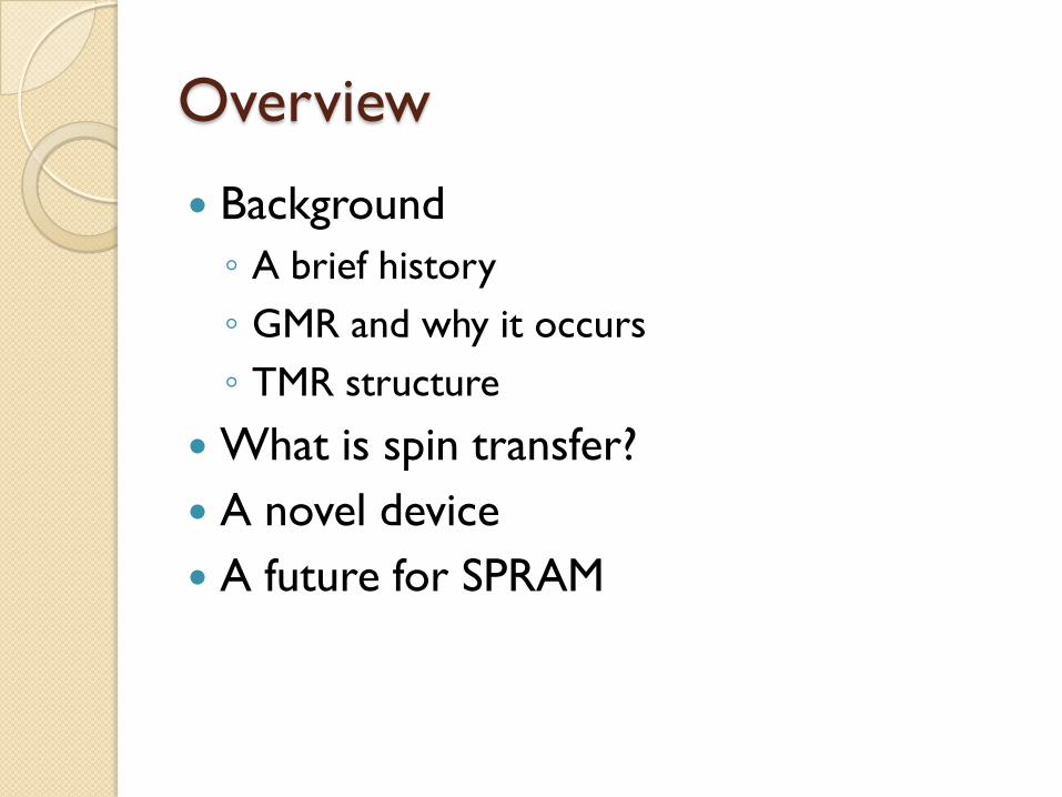
Overview
Background
◦ A brief history
◦ GMR and why it occurs
◦ TMR structure
What is spin transfer?
A novel device
A future for SPRAM

Background
Timeline
Lord Kelvin observes
anisotropic magnetic
resistance (AMR) 1857 Sir Neville Mott develops
model for the “anomalous”
electrical resistivities of the ferromagnetic transition-
metals 1936
Michel Julliere discovers TMR
at very low temperatures 1975
Fert and Grünberg discover
GMR 1988
IBM uses GMR devices in read
heads for hard drives
Terunobu Miyazaki discovers
room temperature TMR 1995
Slonczewski and Berger
propose concept of "spin
transfer" 1996
Predicted TMR ratios of 1000%
using MgO barrier layer 2001
First prototype 2MBit SPRAM
device 2007
1857 1877 1897 1917 1937 1957 1977 1997 2017
Events leading to the discovery of Spin Transfer Torque RAM

BackgroundAnisotropic Magneto-resistance (AMR)
1857- Lord Kelvin
discovers AMR using Fe
and Ni
“…I found that iron, when subjected to magnetic force, acquires an increase of
resistance to the conduction of electricity across, the lines of magnetization…the
electric conductivity of nickel is similarly influenced by magnetism, but to a greater
degree…”
-Lord Kelvin, Proceedings of the Royal Society of London, Vol. 8, 1857, pp. 546550

Background
Giant Magneto-resistance (GMR) The concept for “spin transfer” evolved
from the physical principles of GMR
Fathers of GMR
Albert Fert Peter Grünberg

Background
Giant Magneto-resistance (GMR) Spin valve type GMR device
◦ Anti-ferromagnetic (AF)
◦ Pinned Layer- ferromagnetic (FM)
◦ Nonmagnetic (NM)
◦ Free Layer- ferromagnetic (FM)

Background
Giant Magneto-resistance (GMR) External magnetic field switches the
orientation of the free layer between
parallel (P) and anti-parallel (AP)
Resistance in the P-state is lower than the
AP-state (RAP> RP)
Good at differentiating between “1” or
“0” using changes in resistance

Background
Giant Magneto-resistance (GMR) Practical Application IBM HD read heads

Background
GMR why it occurs? 1922 – Stern-Gerlach Experiment
Electrons have intrinsic angular
momentum which depend on their
quantized spin number (ms = ±1/2)

Background
GMR why it occurs? Electrical Resistance is caused by electron
scattering
Probability of scattering depends on the
number of available quantum states for
the electron to scatter into, which
depends strongly on the relative direction
of the electron's spin and the magnetic
field inside the FM layer.

Background
GMR why it occurs? GMR effect in the P and AP states
P-state experiences less scattering
◦ Up spin electrons have no states to scatter
into.

Background Tunneling Magneto-resistance (TMR)
1975 – Discovered by Michel Julliere
◦ At 4.2 K Julliere observed resistance changes
on the order of 14%
◦ His work was disregarded as impractical until
room temperature TMR was achieved in 1995
by Terunobu Miyazaki

Background
TMR structure SPRAM devices implements a TMR
structure
◦ Main differences between TMR and GMR
GMR has a middle NM layer whereas TMR uses an insulator
TMR uses current induced magnetic fields to switch from AP to P states and vice versa
TMR achieves resistance ratio results on the order 500% (GMR ~ 50%)
Today’s HD readers are predominantly using TMR structures

Background TMR structure
Cobalt
ferromagnetic
layers
Magnesium Oxide
insulating barrier
layer

Background
TMR structure Why Co?
◦ Cobalt is missing 3 electron in the 3d level 1936 - Sir Neville Mott’s model states that the 3d level
electrons act as scatterers near the fermi level.
The density of states at the fermi energy is mostly spin down meaning Co has more quantum states for scattering.

Background TMR structure
Why MgO?
◦ Magnesium oxide has a cubic crystalline
structure which aids in conservation of
electron momentum transfer
◦ 2001 – predicted TMR ratio of 1000% using
this insulating layer.

What is Spin Transfer?
1996 – Slonczewski and Berger propose
the idea of spin transfer
◦ “When a current of polarized electrons
enters a ferro-magnet, there is generally a
transfer of angular momentum between
propagating electrons and the magnetization
of the film.”

What is Spin Transfer?
In short – instead of changing the magnetic field
externally it is done by polarized currents.
The result – Similar to GMR/TMR a resistance
change is seen from AP to P states.

A Novel Device
A group developed a 1.8 V 2Mb SPRAM
chip
◦ Using NiFe(2nm)/ CoFe(1nm)/MgO(1nm)/CoFe(1nm)
TMR memory cell

A Novel Device
Components of one Bit
◦ Bit Line (BL) – where state is read
◦ Source Line (SL) – current source
◦ Word Line (WL) – current state regulator
◦ TMR device – memory cell

A Novel Device
Writing “0”s and “1”s

Novel Device
Major Pitfalls
◦ Switching Current Direction
In order to write “0” or “1” current must be either
into or out of SL
◦ Reading Bits without accidental writing
Reading is similar to writing
There exists a critical current density Jc- for
parallelizing and Jc+ for anti-parallelizing.

Novel Device
Current Switching
◦ Use a flip flop gate
depending on inputs
of SALT and SALB
Example
SALT = High (H) +
SALB = Low (L) =
parallelizing (BL to SL)

Novel Device
Parallelizing
Anti-Parallelizing

Novel Device
Accidental writing while reading (accidental spin reversal)
Disturbance – a measure of likelihood of spin reversal. ◦ Parallelizing direction has larger disturbance when reading
AP-state, therefore lower chance of spin reversal.

Novel Device
Testing this hypothesis by varying the TMR ratio
For P direction – As TMR ratio increases the possibility of spin reversal decreases.
For AP direction – does not depend on TMR ratio.

Novel Device
Finished Product

Novel Device
Proven 10 year life cycle
◦ No degradation of RAP / RP after 1 billion
write cycles
Fast read/write
Non-volatile
Instant-ON capable
Low energy
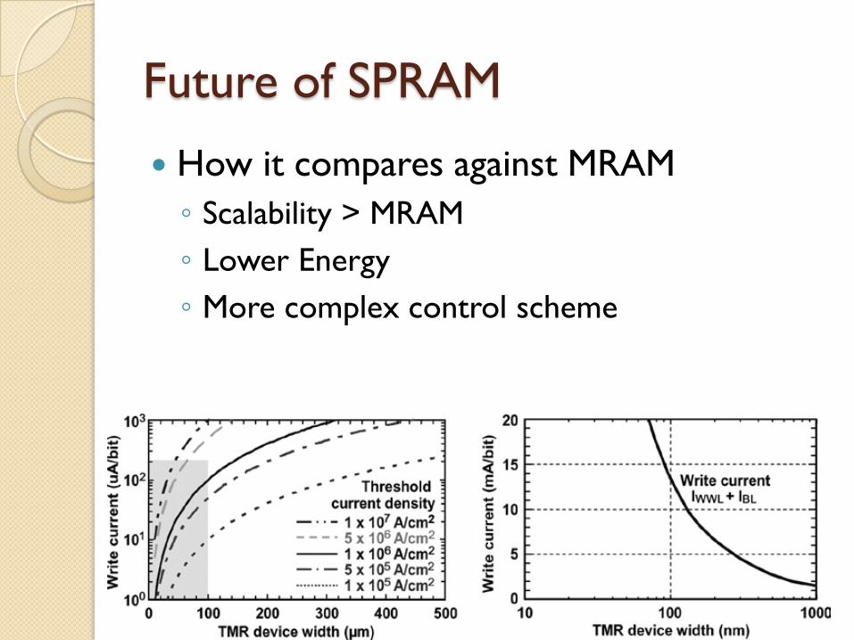
Future of SPRAM
How it compares against MRAM
◦ Scalability > MRAM
◦ Lower Energy
◦ More complex control scheme

Future of SPRAMPotential for higher speeds
Research conducted by Sarah Gerretsen,
University of California
◦ TMR device of Co (20nm) /MgO (5nm) /Co
(5nm) with a switching current of 1.96mA
resulted in a 0.104ns P to AP state switching
time
Work Cited1. J. C. Slonczewski, J. Magn. Magn. Mater. 159, L1 (1996); 195, L261 (1999).
2. L. Berger, Phys. Rev. B 54, 9353 (1996); J. Appl. Phys. 81, 4880 (1997); Phys. Rev. B 59, 11465 (1999); J. Appl. Phys. 89,
5521 (2001); “Interaction of electrons with spinwaves in the bulk and in multilayers cond-mat”/0203314.
3. M.D. Stiles & A. Zangwill. “Anatomy of Spin-Transfer Torque.” May 2002
4. Alain Schuhl, Daniel Lacour, C. R. Physique 6 (2005) 945–955
5. P. M. Levy 2008. “An Idiosyncratic History of Giant Magnetoresistance”. NSDL Classic Articles in Context. Issue 2,
December 2008. <http:// wiki.nsdl.org/index.php/PALE:ClassicArticles/GMR>
6. Butler, W.H., Zhang, X.G., Schulthess, T.C. & MacLaren, J.M., 2001. “Spin-dependent Tunneling Conductance of
Fe|MgO|Fe Sandwiches.” Phys. Rev. B 63, 054416 and Mathon, J. & A. Umerski, A., 2001. “Theory of Tunneling
Magnetoresistance of an Epitaxial Fe/MgO/Fe(001) Junction.” Phys. Rev. 63, 220403(R)
7. S. Maekawa & T. Shinjo.“Spin Dependent Transport in Magnetic Nanostructures.” (Eds.) London: Taylor and Francis
(2002) pg. 81
8. Kawahara, T., Takemura, R., Miura, K., Hayakawa, J., Ikeda, S., Lee, Y.M., Sasaki, R., Goto,Y., Ito,K., Meguro, T.,
Matsukura, F., Takahashi, H., Matsuoka, H. & Ohno, H. . “2 Mb SPRAM (SPin-Transfer Torque RAM) With Bit-by-Bit
Bi-Directional Current Write and Parallelizing-Direction Current Read.” IEEE Journal of Solid-State Circuits, vol. 43,
NO. 1, January 2008 pg. 109-120.
9. Sarah Gerretsen. “Spin Transfer Torque in Ferromagnetic Materials.” Department of Physics and Astronomy,
University of California, Los Angles, Ca, 90095
10. J. C. Sankey, Y.-T. Cui, R. A. Buhrman, D. C. Ralph, J. Z. Sun, J. C. Slonczewski. “Measurement of the Spin-Transfer-
Torque Vector in Magnetic Tunnel Junctions.” Nature Physics 4, 67 - 71 (2008)
11. V. K. Dugaev, J. Barnas. “Classical description of current-induced spin-transfer torque in multilayer structures.” J. Appl.
Phys. 97, 023902 (2005)
12. Evgeny Y. Tsymbal. "Magnetic Tunnel Junction." <http://
physics.unl.edu/~tsymbal/tsymbal_files/TMR/sdt_files/page0001.html>.

Questions