Low-Emission Designs With ISOW7841 Integrated Signal … · also duty-cycles the power-converter to...
14
1 SLLA368A – May 2017 – Revised August 2017 Submit Documentation Feedback Copyright © 2017, Texas Instruments Incorporated Low-Emission Designs With ISOW7841 Integrated Signal and Power Isolator Application Report SLLA368A – May 2017 – Revised August 2017 Low-Emission Designs With ISOW7841 Integrated Signal and Power Isolator Anand Reghunathan Koteshwar Rao Anant Kamath ABSTRACT The ISOW7841 integrated signal and power isolation device simplifies system design and reduces board area. The use of low-inductance micro-transformers in the ISOW7841 device necessitates the use of high- frequency switching, resulting in higher radiated emissions compared to discrete solutions. The ISOW7841 device uses on-chip circuit techniques to reduce emissions compared to competing solutions. Techniques such as lower supply operation, the use of interlayer stitching capacitance, filters, and common-mode chokes can further reduce radiated emissions at the system level. Contents 1 Introduction ................................................................................................................... 2 2 Use 3.3-V Input Supply Where Possible.................................................................................. 4 3 Input and Output Decoupling Capacitors, Input Ballast Resistor, Ferrite Beads .................................... 4 4 Interlayer Side 1-to-Side 2 Capacitor ..................................................................................... 5 5 Direct and Capacitive Connection to Protection Earth .................................................................. 9 6 Using Common-Mode Chokes ............................................................................................. 9 7 Precautions During EMI Measurements ................................................................................ 10 8 Quasi-Peak versus Peak Detection ...................................................................................... 11 9 Conclusion .................................................................................................................. 12 10 References .................................................................................................................. 12 List of Figures 1 ISOW7841 Single-Chip Power and Data Isolation ...................................................................... 2 2 Common-Mode Currents Across the Isolation Barrier form a Large Return Loop .................................. 3 3 Radiated Emissions of the ISOW7841 vs a Competitive Device at 5-V Input and 80-mA Load .................. 3 4 Radiated Emissions of ISOW7841 at 5-V Input vs at 3.3-V Input ..................................................... 4 5 Supply Decoupling Capacitors and Input Ballasting Resistor.......................................................... 4 6 ISOW7841 Evaluation Module ............................................................................................. 5 7 Side 1-to-Side 2 High-Voltage Capacitor Reduces the Common-Mode Current-Loop Area ...................... 6 8 Solving for C i for the PCB in Using ....................................................................................... 7 9 3-D Diagram of PCB Layers With Interlayer Stitching Capacitance .................................................. 7 10 ISOW7841 Emissions With and Without a 30-pF Stitching Capacitance at a 5-V Input and 80-mA Load Current ........................................................................................................................ 8 11 Triangle Corners Implemented to Enhance High-Voltage Performance ............................................. 8 12 Direct and Capacitive Connection to PE in an Isolated RS-485 Application Using ISOW7841 ................... 9 13 Common-Mode Chokes on Input and Output Power Supply and I/O Lines Reduce Emissions................. 10 14 ISOW7841 Emissions Measurement Setup (CISPR 22) ............................................................. 11 15 Quasi Peak vs Peak Measurements With ISOW7841 ................................................................ 12
Transcript of Low-Emission Designs With ISOW7841 Integrated Signal … · also duty-cycles the power-converter to...
1SLLA368A–May 2017–Revised August 2017Submit Documentation Feedback
Copyright © 2017, Texas Instruments Incorporated
Low-Emission Designs With ISOW7841 Integrated Signal and Power Isolator
Application ReportSLLA368A–May 2017–Revised August 2017
Low-Emission Designs With ISOW7841 Integrated Signaland Power Isolator
Anand ReghunathanKoteshwar RaoAnantKamath
ABSTRACTThe ISOW7841 integrated signal and power isolation device simplifies system design and reduces boardarea. The use of low-inductance micro-transformers in the ISOW7841 device necessitates the use of high-frequency switching, resulting in higher radiated emissions compared to discrete solutions. The ISOW7841device uses on-chip circuit techniques to reduce emissions compared to competing solutions. Techniquessuch as lower supply operation, the use of interlayer stitching capacitance, filters, and common-modechokes can further reduce radiated emissions at the system level.
Contents1 Introduction ................................................................................................................... 22 Use 3.3-V Input Supply Where Possible.................................................................................. 43 Input and Output Decoupling Capacitors, Input Ballast Resistor, Ferrite Beads .................................... 44 Interlayer Side 1-to-Side 2 Capacitor ..................................................................................... 55 Direct and Capacitive Connection to Protection Earth.................................................................. 96 Using Common-Mode Chokes ............................................................................................. 97 Precautions During EMI Measurements ................................................................................ 108 Quasi-Peak versus Peak Detection...................................................................................... 119 Conclusion .................................................................................................................. 1210 References .................................................................................................................. 12
List of Figures
1 ISOW7841 Single-Chip Power and Data Isolation ...................................................................... 22 Common-Mode Currents Across the Isolation Barrier form a Large Return Loop .................................. 33 Radiated Emissions of the ISOW7841 vs a Competitive Device at 5-V Input and 80-mA Load .................. 34 Radiated Emissions of ISOW7841 at 5-V Input vs at 3.3-V Input..................................................... 45 Supply Decoupling Capacitors and Input Ballasting Resistor.......................................................... 46 ISOW7841 Evaluation Module ............................................................................................. 57 Side 1-to-Side 2 High-Voltage Capacitor Reduces the Common-Mode Current-Loop Area ...................... 68 Solving for Ci for the PCB in Using ....................................................................................... 79 3-D Diagram of PCB Layers With Interlayer Stitching Capacitance .................................................. 710 ISOW7841 Emissions With and Without a 30-pF Stitching Capacitance at a 5-V Input and 80-mA Load
Current ........................................................................................................................ 811 Triangle Corners Implemented to Enhance High-Voltage Performance ............................................. 812 Direct and Capacitive Connection to PE in an Isolated RS-485 Application Using ISOW7841 ................... 913 Common-Mode Chokes on Input and Output Power Supply and I/O Lines Reduce Emissions................. 1014 ISOW7841 Emissions Measurement Setup (CISPR 22) ............................................................. 1115 Quasi Peak vs Peak Measurements With ISOW7841 ................................................................ 12
16
15
14
12
11
10
9
1
2
3
4
5
6
7
8
13
GND1
VCC
GND2
VISO
GND1 GND2
NC SEL
OUTA/INAINA/OUTA
OUTB/INBINB/OUTB
OUTC/INCINC/OUTC
OUTD/INDIND/OUTD
DC-DCPrimary
DC-DC Feedback
+Quad
Isolators
ISOW7841
DC-DCSecondary
DC-DC Feedback
+Quad
Isolators
Copyright © 2017, Texas Instruments Incorporated
Introduction www.ti.com
2 SLLA368A–May 2017–Revised August 2017Submit Documentation Feedback
Copyright © 2017, Texas Instruments Incorporated
Low-Emission Designs With ISOW7841 Integrated Signal and Power Isolator
TrademarksAll trademarks are the property of their respective owners.
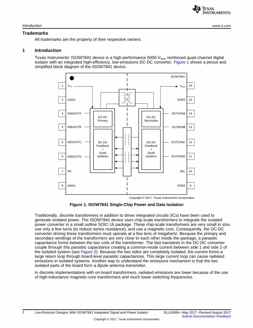
1 IntroductionTexas Instruments’ ISOW7841 device is a high-performance 5000-VRMS reinforced quad-channel digitalisolator with an integrated high-efficiency, low-emissions DC-DC converter. Figure 1 shows a pinout andsimplified block diagram of the ISOW7841 device.
Figure 1. ISOW7841 Single-Chip Power and Data Isolation
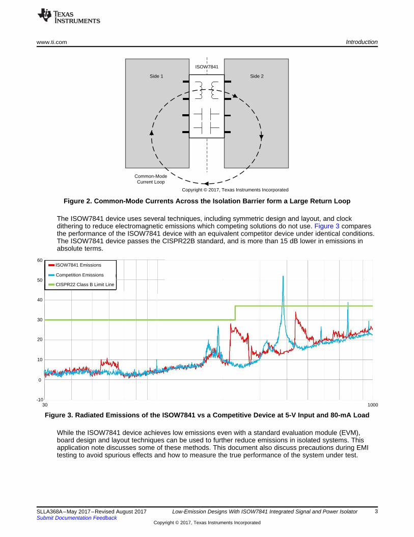
Traditionally, discrete transformers in addition to driver integrated circuits (ICs) have been used togenerate isolated power. The ISOW7841 device uses chip-scale transformers to integrate the isolatedpower converter in a small outline SOIC-16 package. These chip-scale transformers are very small in size,use only a few turns (to reduce series resistance), and use a magnetic core. Consequently, the DC-DCconverter driving these transformers must operate at a few tens of megahertz. Because the primary andsecondary windings of the transformers are very close to each other inside the package, a parasiticcapacitance forms between the two coils of the transformer. The fast transients in the DC-DC convertercouple through this parasitic capacitance creating a common-mode current between side 1 and side 2 ofthe isolated system (see Figure 2). Because the two sides are completely isolated, the current forms alarge return loop through board-level parasitic capacitances. This large current loop can cause radiatedemissions in isolated systems. Another way to understand the emissions mechanism is that the twoisolated parts of the board form a dipole antenna transmitter.
In discrete implementations with on-board transformers, radiated emissions are lower because of the useof high-inductance magnetic-core transformers and much lower switching frequencies.
ISOW7841 Emissions
Competition Emissions
CISPR22 Class B Limit Line
60
50
40
30
20
10
0
-1030 1000
Side 1 Side 2
Common-Mode Current Loop
ISOW7841
Copyright © 2017, Texas Instruments Incorporated
www.ti.com Introduction
3SLLA368A–May 2017–Revised August 2017Submit Documentation Feedback
Copyright © 2017, Texas Instruments Incorporated
Low-Emission Designs With ISOW7841 Integrated Signal and Power Isolator
Figure 2. Common-Mode Currents Across the Isolation Barrier form a Large Return Loop
The ISOW7841 device uses several techniques, including symmetric design and layout, and clockdithering to reduce electromagnetic emissions which competing solutions do not use. Figure 3 comparesthe performance of the ISOW7841 device with an equivalent competitor device under identical conditions.The ISOW7841 device passes the CISPR22B standard, and is more than 15 dB lower in emissions inabsolute terms.
Figure 3. Radiated Emissions of the ISOW7841 vs a Competitive Device at 5-V Input and 80-mA Load
While the ISOW7841 device achieves low emissions even with a standard evaluation module (EVM),board design and layout techniques can be used to further reduce emissions in isolated systems. Thisapplication note discusses some of these methods. This document also discuss precautions during EMItesting to avoid spurious effects and how to measure the true performance of the system under test.

VCC VISO
GND1 GND2Loop 1 Loop 2
Bac
kpla
ne P
ower
To LoadL1
ISOW7841
Loop 3 Loop 4
Copyright © 2017, Texas Instruments Incorporated
C3 C2 C1CF
RF
C1 C2 C3
60
50
40
30
20
10
0
-1030 1000
ISOW7841 (5 V) Emissions
CISPR22 Class B Limit Line
ISOW7841 (3.3 V) Emissions
Use 3.3-V Input Supply Where Possible www.ti.com
4 SLLA368A–May 2017–Revised August 2017Submit Documentation Feedback
Copyright © 2017, Texas Instruments Incorporated
Low-Emission Designs With ISOW7841 Integrated Signal and Power Isolator
2 Use 3.3-V Input Supply Where PossibleThe ISOW7841 supports both 3.3-V and 5-V input supply operation. Compared to 5-V operation, at 3.3-Voperation the slew rates of the internal DC-DC converter are lower because of the lower voltage driveavailable to the power transistors. Lower slew rates reduce the common-mode current across the isolationbarrier, leading to lower radiated emissions. As shown in Figure 4, the emissions with a 3.3-V input supplyare much lower than with a 5-V supply. Where possible, TI recommends operating the ISOW7841 devicewith a 3.3-V input supply.
Figure 4. Radiated Emissions of ISOW7841 at 5-V Input vs at 3.3-V Input
3 Input and Output Decoupling Capacitors, Input Ballast Resistor, Ferrite BeadsThe ISOW7841 device uses high-frequency switching to compensate for low transformer inductance, andalso duty-cycles the power-converter to provide the required output DC load while maintaining regulation.Whenever the converter is on, a high current draw from the input supply, VCC, occurs. This current haslow-frequency content (roughly proportional to the closed-loop regulation bandwidth) and high-frequencycontent at the switching frequency and harmonics of the DC-DC converter.
Figure 5. Supply Decoupling Capacitors and Input Ballasting Resistor

Stitching Vias Along Board Edges
Bank of Decoupling Capacitors Close to the IC
Stitching Vias atEdges of a Fill
www.ti.com Interlayer Side 1-to-Side 2 Capacitor
5SLLA368A–May 2017–Revised August 2017Submit Documentation Feedback
Copyright © 2017, Texas Instruments Incorporated
Low-Emission Designs With ISOW7841 Integrated Signal and Power Isolator
An input capacitor bank of different capacitors (C1 = 100 nF, C2 = 1 µF, C3 = 100 nF) at the input of theIC filters out a lot of the high-frequency content and prevents it from propagating to the backplane supplyrouting. Placing these capacitors as close to the IC (see Figure 5) as possible is critical to limit the area ofloop 1. Place the smallest-value capacitor closest to the IC. A similar bank of capacitors placed on theoutput side filters out switching current on the secondary side of the DC-DC converter. Minimizing the areaof loop 2 is important.
Despite the decoupling capacitors, the backplane supply routing can still draw some high-frequency andlow-frequency current (a peak current of 100s of milliamperes lasting several microseconds) depending onthe output impedance of the supply network. If the input supply routing is long, a ballasting resistor (RF)and an additional larger capacitor (CF, 100 µF) can prevent current into the input supply routing (loop 3)leading to lower radiated emissions.
Figure 6 shows the image of the ISOW7841 evaluation module (EVM) and the placement of decouplingcapacitors. In this layout, stitching vias along the board edge that connect all ground planes creates aFaraday shield. This shield prevents any radiation from noisy inner traces or planes.
Figure 6. ISOW7841 Evaluation Module
4 Interlayer Side 1-to-Side 2 CapacitorAs previously discussed, the common-mode current from side 1 to side 2 and a large return loop are themain causes of emissions in isolated systems. One way of minimizing the current loop is to include a high-voltage capacitor from side 1 to side 2 and place it as close to the IC as possible as shown in Figure 7.

Side 1 Side 2
Side 1-to-Side 2Capacitor
ISOW7841
Common-mode current loop is much smaller
Copyright © 2017, Texas Instruments Incorporated
Interlayer Side 1-to-Side 2 Capacitor www.ti.com
6 SLLA368A–May 2017–Revised August 2017Submit Documentation Feedback
Copyright © 2017, Texas Instruments Incorporated
Low-Emission Designs With ISOW7841 Integrated Signal and Power Isolator
Figure 7. Side 1-to-Side 2 High-Voltage Capacitor Reduces the Common-Mode Current-Loop Area
The capacitors suitable for such use include high-voltage Y2 capacitors (surface-mount device [SMD] orleaded with appropriate creepage, or clearance levels) commonly used in power supplies. Using Y2capacitors on the printed circuit board (PCB) introduces lead inductances on both sides of the capacitor, inaddition to the parasitic inductance of the capacitor, making the capacitor ineffective at frequencies higherthan 200MHz. One way to create a low-inductance capacitance is by overlapping internal PCB layers.
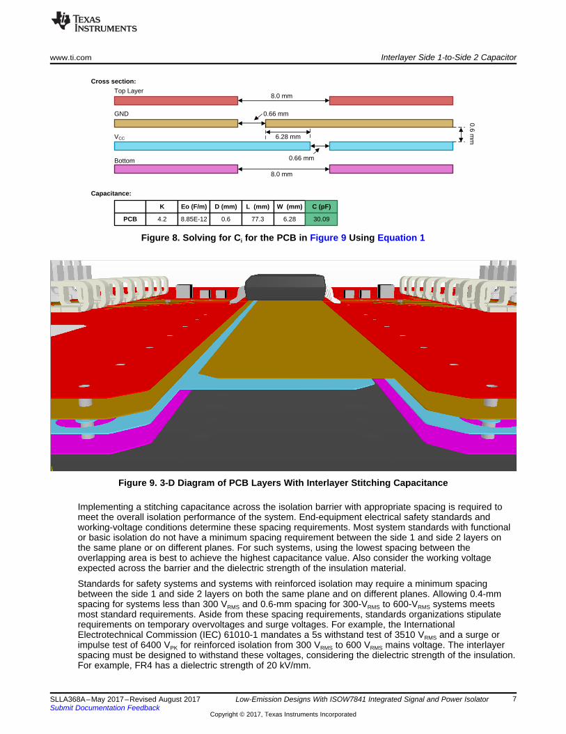
Consider a four-layer PCB with the top layer for the signal, layer 2 for ground, layer 3 for VCC, and thebottom layer for the signal. Because of system isolation, PCB layers are separated into two groups: side 1layers (forming signal1, GND1, and VCC1) and side 2 layers (forming signal2, GND2, and VCC2). Extendingthe internal reference layers (GND and VCC) on either side of the isolation barrier (as shown in Figure 8)creates an overlap of internal layers. This overlap area, formed by the extension of the GND1 and VCC2layers with FR4 material between them acting as a dielectric, creates a stitching capacitance betweenGND1 and VCC2. For fast transient common-mode currents, both GND and VCC points are considered to bethe same references (similar to AC analysis). Therefore, interlayer stitching capacitance forms betweenthe reference points of side 1 and side 2. Figure 9 shows a 3-D representation of the interlayer stitchingcapacitance created in a four-layer PCB.
Use Equation 1 to calculate the equivalent capacitance formed between the sides.
where• ε = εoεr
• Ci is the interlayer stitching capacitance.• εo is the absolute permittivity of air (8.854 pF/m).• εr is the relative permittivity of the dielectric (4.2 for FR4)• A is the overlapping area.• d is the distance between the GND and VCC layers. (1)
From Equation 1, solving for the interlayer stitching capacitance (Ci) for the PCB in Figure 9 wouldproduce an approximate value of 30 pF.
Cross section:Top Layer
8.0 mm
GND 0.66 mm
VCC 6.28 mm
Bottom
8.0 mm
0.66 mm
0.6 mm
PCB 4.2
K Eo (F/m) D (mm) L (mm) W (mm) C (pF)
8.85E-12 0.6 77.3 6.28 30.09
Capacitance:
www.ti.com Interlayer Side 1-to-Side 2 Capacitor
7SLLA368A–May 2017–Revised August 2017Submit Documentation Feedback
Copyright © 2017, Texas Instruments Incorporated
Low-Emission Designs With ISOW7841 Integrated Signal and Power Isolator
Figure 8. Solving for Ci for the PCB in Figure 9 Using Equation 1
Figure 9. 3-D Diagram of PCB Layers With Interlayer Stitching Capacitance
Implementing a stitching capacitance across the isolation barrier with appropriate spacing is required tomeet the overall isolation performance of the system. End-equipment electrical safety standards andworking-voltage conditions determine these spacing requirements. Most system standards with functionalor basic isolation do not have a minimum spacing requirement between the side 1 and side 2 layers onthe same plane or on different planes. For such systems, using the lowest spacing between theoverlapping area is best to achieve the highest capacitance value. Also consider the working voltageexpected across the barrier and the dielectric strength of the insulation material.
Standards for safety systems and systems with reinforced isolation may require a minimum spacingbetween the side 1 and side 2 layers on both the same plane and on different planes. Allowing 0.4-mmspacing for systems less than 300 VRMS and 0.6-mm spacing for 300-VRMS to 600-VRMS systems meetsmost standard requirements. Aside from these spacing requirements, standards organizations stipulaterequirements on temporary overvoltages and surge voltages. For example, the InternationalElectrotechnical Commission (IEC) 61010-1 mandates a 5s withstand test of 3510 VRMS and a surge orimpulse test of 6400 VPK for reinforced isolation from 300 VRMS to 600 VRMS mains voltage. The interlayerspacing must be designed to withstand these voltages, considering the dielectric strength of the insulation.For example, FR4 has a dielectric strength of 20 kV/mm.

ISOW7841 Emissions (Without Stitching Capacitance)60
50
40
30
20
10
0
-1030 1000
CISPR22 Class B Limit Line
ISOW7841 (With Stitching Capacitance)
Interlayer Side 1-to-Side 2 Capacitor www.ti.com
8 SLLA368A–May 2017–Revised August 2017Submit Documentation Feedback
Copyright © 2017, Texas Instruments Incorporated
Low-Emission Designs With ISOW7841 Integrated Signal and Power Isolator
Figure 10 shows the reduction in radiated emissions from the ISOW7841 device with the use of aninterlayer stitching capacitance. With only a 30-pF capacitor between the two sides, an improvement of10dB to 20dB is achieved. Higher stitching values can provide progressively higher attenuation inemissions.
Figure 10. ISOW7841 Emissions With and Without a 30-pF Stitching Capacitance at a 5-V Input and 80-mA Load Current
Apart from maintaining the spacing across the barrier, extra care must be given at the edges of the PCB.At the edges, the planes can be exposed to air. Because opposite voltages come close to the edge of theboard, these opposing voltages could lead to electric field stress and then air breakdown along the edge.Sharp edges and corners can also contribute to the air breaking down further because they increase theintensity of the electric field in the vicinity of the sharp edge, leading to a breakdown path for high-voltageimpulse tests. To avoid such scenarios, pull in the inner layers at the edge of the PCB, and modify sharpedges into triangle-cut shapes, which will spread the charge density. Figure 11 shows an example of suchan implementation. Rounding the corners and planes can also further enhance the solution.
Figure 11. Triangle Corners Implemented to Enhance High-Voltage Performance
VCC VISO
GND1GND2
µC RS-485Transceiver
A
B
PE (Protective Earth)
VIN
ISOW7841
Copyright © 2017, Texas Instruments Incorporated
www.ti.com Direct and Capacitive Connection to Protection Earth
9SLLA368A–May 2017–Revised August 2017Submit Documentation Feedback
Copyright © 2017, Texas Instruments Incorporated
Low-Emission Designs With ISOW7841 Integrated Signal and Power Isolator
While the inner layers of the PCB completely surrounded by dielectric allow relatively lower spacing (aspreviously discussed), the top and bottom signal layers must maintain much higher spacing. This spacingis based on the expected temporary overvoltage, impulse voltages, and environmental conditions such asaltitude and pollution degree.
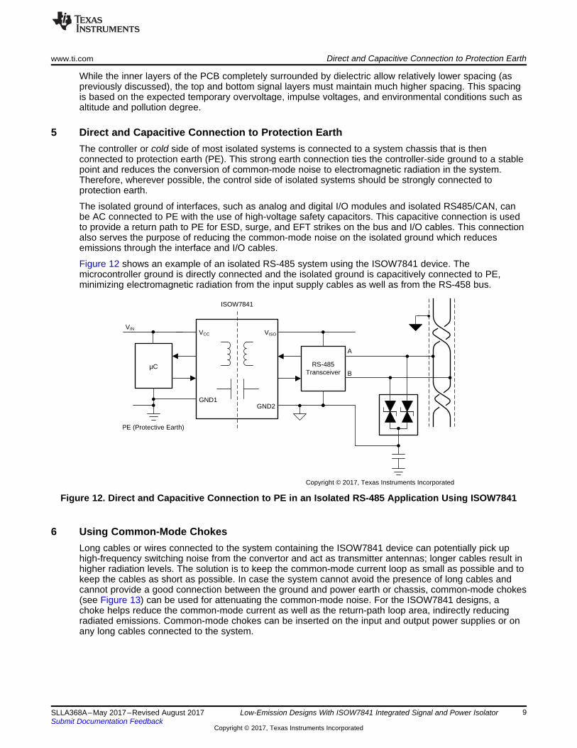
5 Direct and Capacitive Connection to Protection EarthThe controller or cold side of most isolated systems is connected to a system chassis that is thenconnected to protection earth (PE). This strong earth connection ties the controller-side ground to a stablepoint and reduces the conversion of common-mode noise to electromagnetic radiation in the system.Therefore, wherever possible, the control side of isolated systems should be strongly connected toprotection earth.
The isolated ground of interfaces, such as analog and digital I/O modules and isolated RS485/CAN, canbe AC connected to PE with the use of high-voltage safety capacitors. This capacitive connection is usedto provide a return path to PE for ESD, surge, and EFT strikes on the bus and I/O cables. This connectionalso serves the purpose of reducing the common-mode noise on the isolated ground which reducesemissions through the interface and I/O cables.
Figure 12 shows an example of an isolated RS-485 system using the ISOW7841 device. Themicrocontroller ground is directly connected and the isolated ground is capacitively connected to PE,minimizing electromagnetic radiation from the input supply cables as well as from the RS-458 bus.
Figure 12. Direct and Capacitive Connection to PE in an Isolated RS-485 Application Using ISOW7841
6 Using Common-Mode ChokesLong cables or wires connected to the system containing the ISOW7841 device can potentially pick uphigh-frequency switching noise from the convertor and act as transmitter antennas; longer cables result inhigher radiation levels. The solution is to keep the common-mode current loop as small as possible and tokeep the cables as short as possible. In case the system cannot avoid the presence of long cables andcannot provide a good connection between the ground and power earth or chassis, common-mode chokes(see Figure 13) can be used for attenuating the common-mode noise. For the ISOW7841 designs, achoke helps reduce the common-mode current as well as the return-path loop area, indirectly reducingradiated emissions. Common-mode chokes can be inserted on the input and output power supplies or onany long cables connected to the system.
VCC VISO
GND1 GND2
To Load
ISOW7841
Common-ModeChoke0
0
VIN
Copyright © 2017, Texas Instruments Incorporated
C3 C2 C1 C4 C5 C6CF
Common-ModeChoke0
0GNDIN
Precautions During EMI Measurements www.ti.com
10 SLLA368A–May 2017–Revised August 2017Submit Documentation Feedback
Copyright © 2017, Texas Instruments Incorporated
Low-Emission Designs With ISOW7841 Integrated Signal and Power Isolator
(1) Any I/O cables should have common-mode choke with respect to GND.
Figure 13. Common-Mode Chokes on Input and Output Power Supply and I/O Lines Reduce Emissions
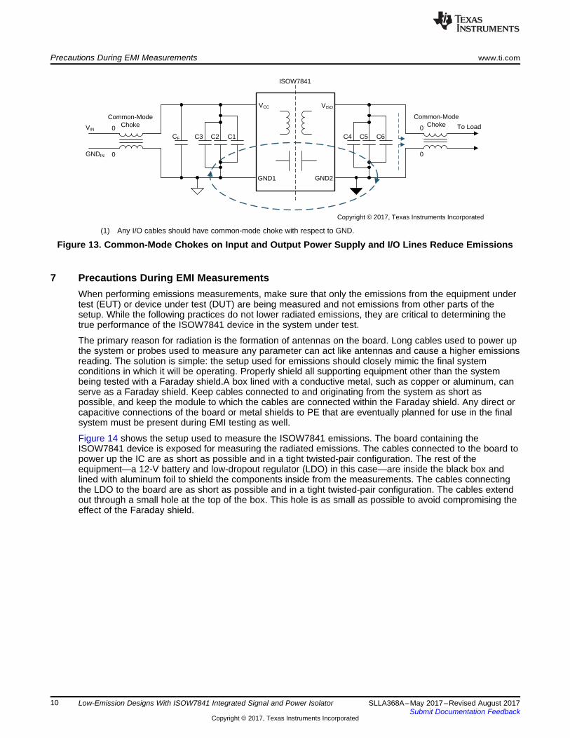
7 Precautions During EMI MeasurementsWhen performing emissions measurements, make sure that only the emissions from the equipment undertest (EUT) or device under test (DUT) are being measured and not emissions from other parts of thesetup. While the following practices do not lower radiated emissions, they are critical to determining thetrue performance of the ISOW7841 device in the system under test.
The primary reason for radiation is the formation of antennas on the board. Long cables used to power upthe system or probes used to measure any parameter can act like antennas and cause a higher emissionsreading. The solution is simple: the setup used for emissions should closely mimic the final systemconditions in which it will be operating. Properly shield all supporting equipment other than the systembeing tested with a Faraday shield.A box lined with a conductive metal, such as copper or aluminum, canserve as a Faraday shield. Keep cables connected to and originating from the system as short aspossible, and keep the module to which the cables are connected within the Faraday shield. Any direct orcapacitive connections of the board or metal shields to PE that are eventually planned for use in the finalsystem must be present during EMI testing as well.
Figure 14 shows the setup used to measure the ISOW7841 emissions. The board containing theISOW7841 device is exposed for measuring the radiated emissions. The cables connected to the board topower up the IC are as short as possible and in a tight twisted-pair configuration. The rest of theequipment—a 12-V battery and low-dropout regulator (LDO) in this case—are inside the black box andlined with aluminum foil to shield the components inside from the measurements. The cables connectingthe LDO to the board are as short as possible and in a tight twisted-pair configuration. The cables extendout through a small hole at the top of the box. This hole is as small as possible to avoid compromising theeffect of the Faraday shield.

Antenna
DUT
Power Supply(12 V Battery + LDO)Enclosed within box
10 Meters
Short Twisted-PairCables
Faraday CageLined With Aluminum
www.ti.com Quasi-Peak versus Peak Detection
11SLLA368A–May 2017–Revised August 2017Submit Documentation Feedback
Copyright © 2017, Texas Instruments Incorporated
Low-Emission Designs With ISOW7841 Integrated Signal and Power Isolator
Figure 14. ISOW7841 Emissions Measurement Setup (CISPR 22)
If the supply connections are long wires coming from a power supply placed far away from the DUT, thencommon-mode chokes are recommended near the DUT so that the emissions are not unnecessarilyenhanced by the long wires. By using common-mode chokes, emissions of the actual setup are measuredand the effect of the long cables is nullified.
Any extra components required on the board, such as load resistors, must be soldered directly to theboard rather than connecting them to the board using long wires.
8 Quasi-Peak versus Peak DetectionAccording to the CISPR 22 standard, the radiated emissions specification is specified as a quasi-peaklimit, although the peak-detector measurement can typically be used to get a quick result.
The ISOW7841 device uses clock dithering to change the switching frequencies across a small bandinstead of concentrating all of the power at one single peak. Techniques such as this lower the peak scanlevels and also show significantly better results when subjected to quasi-peak scans. At lower loadoperations, the power of radiated emissions is less because the DC-DC converter is on for a much shortertime compared to the full load condition. This lower power is reflected as a significant improvement in thequasi-peak results.
Texas Instruments recommends taking a peak-detector measurement first to find out the frequencies forthe worst-case measurements. Then take a quasi-peak measurement at those frequencies to estimate thetrue margin from the CISPR 22B quasi-peak limit line.
Figure 15 shows the CISPR 22B measurement results with the ISOW7841 device. Up to 8.8-dBimprovements occur with quasi-peak (QP) measurement compared to a peak-detector measurement.

240
240
465
465
676
676
H
V
V
H
H
V
240
240
465
465
676
676
V
H
H
V
H
V
18
20
32
29
39
41
20
19
30
32
38
40
11.8
13
24.5
21
30.2
32.5
13.3
13
23.6
26.3
31.6
34.5
Frequency (MHz) Polarization Peak (dBuV/m) QP (dBuV/m) Improvement (dB)
6.2
7
7.5
8
8.8
8.6
6.7
6
6.4
5.7
6.4
5.5
ISOW78415 V to 3.3 V at 5 mA
ISOW78415 V to 3.3 V at 80 mA
Conclusion www.ti.com
12 SLLA368A–May 2017–Revised August 2017Submit Documentation Feedback
Copyright © 2017, Texas Instruments Incorporated
Low-Emission Designs With ISOW7841 Integrated Signal and Power Isolator
Figure 15. Quasi Peak vs Peak Measurements With ISOW7841
9 ConclusionThe ISOW7841 integrated data and power isolator simplifies system designs and reduces board area.Through chip-design techniques, the ISOW7841 device reduces electromagnetic emissions by more than15 dB when compared to competition solutions. However, techniques such as lower supply operation andthe use of interlayer stitching capacitance, filters, and common-mode chokes can further reduce radiatedemissions at the system level. Care should be taken during emissions measurement to measure the trueperformance of the system under test. Quasi-peak measurements result in lower readings than peakmeasurements, and should be used to assess the exact margin to the CISPR22B standard.
10 References• Texas Instruments, ISOW7841 High-Efficiency, Low-Emissions, Reinforced Digital Isolator With
Integrated Power product folder• Texas Instruments, 8-ch Isolated High Voltage Analog Input Module with ISOW7841 Reference Design• Texas Instruments, Fully integrated signal and power isolation – applications and benefits white paper• Texas Instruments, Isolated RS-485 With Integrated Signal and Power Reference Design• Texas Instruments, Isolated RS-232 With Integrated Signal and Power Reference Design• Texas Instruments, Size and Cost Optimized Binary Module Reference Design Using Digital Isolator
with Integrated Power Reference Design

www.ti.com Revision History
13SLLA368A–May 2017–Revised August 2017Submit Documentation Feedback
Copyright © 2017, Texas Instruments Incorporated
Revision History
Revision HistoryNOTE: Page numbers for previous revisions may differ from page numbers in the current version.
Changes from Original (May 2017) to A Revision ........................................................................................................... Page
• Changed the IEC specification number in the Interlayer Side 1-to-Side 2 Capacitor section ................................... 7

IMPORTANT NOTICE FOR TI DESIGN INFORMATION AND RESOURCES
Texas Instruments Incorporated (‘TI”) technical, application or other design advice, services or information, including, but not limited to,reference designs and materials relating to evaluation modules, (collectively, “TI Resources”) are intended to assist designers who aredeveloping applications that incorporate TI products; by downloading, accessing or using any particular TI Resource in any way, you(individually or, if you are acting on behalf of a company, your company) agree to use it solely for this purpose and subject to the terms ofthis Notice.TI’s provision of TI Resources does not expand or otherwise alter TI’s applicable published warranties or warranty disclaimers for TIproducts, and no additional obligations or liabilities arise from TI providing such TI Resources. TI reserves the right to make corrections,enhancements, improvements and other changes to its TI Resources.You understand and agree that you remain responsible for using your independent analysis, evaluation and judgment in designing yourapplications and that you have full and exclusive responsibility to assure the safety of your applications and compliance of your applications(and of all TI products used in or for your applications) with all applicable regulations, laws and other applicable requirements. Yourepresent that, with respect to your applications, you have all the necessary expertise to create and implement safeguards that (1)anticipate dangerous consequences of failures, (2) monitor failures and their consequences, and (3) lessen the likelihood of failures thatmight cause harm and take appropriate actions. You agree that prior to using or distributing any applications that include TI products, youwill thoroughly test such applications and the functionality of such TI products as used in such applications. TI has not conducted anytesting other than that specifically described in the published documentation for a particular TI Resource.You are authorized to use, copy and modify any individual TI Resource only in connection with the development of applications that includethe TI product(s) identified in such TI Resource. NO OTHER LICENSE, EXPRESS OR IMPLIED, BY ESTOPPEL OR OTHERWISE TOANY OTHER TI INTELLECTUAL PROPERTY RIGHT, AND NO LICENSE TO ANY TECHNOLOGY OR INTELLECTUAL PROPERTYRIGHT OF TI OR ANY THIRD PARTY IS GRANTED HEREIN, including but not limited to any patent right, copyright, mask work right, orother intellectual property right relating to any combination, machine, or process in which TI products or services are used. Informationregarding or referencing third-party products or services does not constitute a license to use such products or services, or a warranty orendorsement thereof. Use of TI Resources may require a license from a third party under the patents or other intellectual property of thethird party, or a license from TI under the patents or other intellectual property of TI.TI RESOURCES ARE PROVIDED “AS IS” AND WITH ALL FAULTS. TI DISCLAIMS ALL OTHER WARRANTIES ORREPRESENTATIONS, EXPRESS OR IMPLIED, REGARDING TI RESOURCES OR USE THEREOF, INCLUDING BUT NOT LIMITED TOACCURACY OR COMPLETENESS, TITLE, ANY EPIDEMIC FAILURE WARRANTY AND ANY IMPLIED WARRANTIES OFMERCHANTABILITY, FITNESS FOR A PARTICULAR PURPOSE, AND NON-INFRINGEMENT OF ANY THIRD PARTY INTELLECTUALPROPERTY RIGHTS.TI SHALL NOT BE LIABLE FOR AND SHALL NOT DEFEND OR INDEMNIFY YOU AGAINST ANY CLAIM, INCLUDING BUT NOTLIMITED TO ANY INFRINGEMENT CLAIM THAT RELATES TO OR IS BASED ON ANY COMBINATION OF PRODUCTS EVEN IFDESCRIBED IN TI RESOURCES OR OTHERWISE. IN NO EVENT SHALL TI BE LIABLE FOR ANY ACTUAL, DIRECT, SPECIAL,COLLATERAL, INDIRECT, PUNITIVE, INCIDENTAL, CONSEQUENTIAL OR EXEMPLARY DAMAGES IN CONNECTION WITH ORARISING OUT OF TI RESOURCES OR USE THEREOF, AND REGARDLESS OF WHETHER TI HAS BEEN ADVISED OF THEPOSSIBILITY OF SUCH DAMAGES.You agree to fully indemnify TI and its representatives against any damages, costs, losses, and/or liabilities arising out of your non-compliance with the terms and provisions of this Notice.This Notice applies to TI Resources. Additional terms apply to the use and purchase of certain types of materials, TI products and services.These include; without limitation, TI’s standard terms for semiconductor products http://www.ti.com/sc/docs/stdterms.htm), evaluationmodules, and samples (http://www.ti.com/sc/docs/sampterms.htm).
Mailing Address: Texas Instruments, Post Office Box 655303, Dallas, Texas 75265Copyright © 2017, Texas Instruments Incorporated