LogiCORE IP Mutex v1 - Xilinx · LogiCORE IP Mutex v1.00a 5 PG089 October 16, 2012 Product...
38
LogiCORE IP Mutex v1.00a Product Guide PG089 October 16, 2012
-
Upload
nguyenxuyen -
Category
Documents
-
view
246 -
download
0
Transcript of LogiCORE IP Mutex v1 - Xilinx · LogiCORE IP Mutex v1.00a 5 PG089 October 16, 2012 Product...

LogiCORE IP Mutex v1.00a
Product Guide
PG089 October 16, 2012

LogiCORE IP Mutex v1.00a www.xilinx.com 2PG089 October 16, 2012
Table of Contents
SECTION I: SUMMARY
IP Facts
Chapter 1: OverviewFeature Summary. . . . . . . . . . . . . . . . . . . . . . . . . . . . . . . . . . . . . . . . . . . . . . . . . . . . . . . . . . . . . . . . . . 6Licensing and Ordering Information . . . . . . . . . . . . . . . . . . . . . . . . . . . . . . . . . . . . . . . . . . . . . . . . . . . 7
Chapter 2: Product SpecificationStandards Compliance . . . . . . . . . . . . . . . . . . . . . . . . . . . . . . . . . . . . . . . . . . . . . . . . . . . . . . . . . . . . . . 8Performance. . . . . . . . . . . . . . . . . . . . . . . . . . . . . . . . . . . . . . . . . . . . . . . . . . . . . . . . . . . . . . . . . . . . . . 8Resource Utilization. . . . . . . . . . . . . . . . . . . . . . . . . . . . . . . . . . . . . . . . . . . . . . . . . . . . . . . . . . . . . . . . 9Port Descriptions . . . . . . . . . . . . . . . . . . . . . . . . . . . . . . . . . . . . . . . . . . . . . . . . . . . . . . . . . . . . . . . . . 11Register Space . . . . . . . . . . . . . . . . . . . . . . . . . . . . . . . . . . . . . . . . . . . . . . . . . . . . . . . . . . . . . . . . . . . 14
Chapter 3: Designing with the CoreGeneral Design Guidelines . . . . . . . . . . . . . . . . . . . . . . . . . . . . . . . . . . . . . . . . . . . . . . . . . . . . . . . . . 17Clocking. . . . . . . . . . . . . . . . . . . . . . . . . . . . . . . . . . . . . . . . . . . . . . . . . . . . . . . . . . . . . . . . . . . . . . . . . 17Resets . . . . . . . . . . . . . . . . . . . . . . . . . . . . . . . . . . . . . . . . . . . . . . . . . . . . . . . . . . . . . . . . . . . . . . . . . . 17Protocol Description . . . . . . . . . . . . . . . . . . . . . . . . . . . . . . . . . . . . . . . . . . . . . . . . . . . . . . . . . . . . . . 18
SECTION II: VIVADO DESIGN SUITE
Chapter 4: Customizing and Generating the CoreGUI . . . . . . . . . . . . . . . . . . . . . . . . . . . . . . . . . . . . . . . . . . . . . . . . . . . . . . . . . . . . . . . . . . . . . . . . . . . . 20GUI Parameters . . . . . . . . . . . . . . . . . . . . . . . . . . . . . . . . . . . . . . . . . . . . . . . . . . . . . . . . . . . . . . . . . . 21
Chapter 5: Constraining the CoreRequired Constraints . . . . . . . . . . . . . . . . . . . . . . . . . . . . . . . . . . . . . . . . . . . . . . . . . . . . . . . . . . . . . . 22Device, Package, and Speed Grade Selections. . . . . . . . . . . . . . . . . . . . . . . . . . . . . . . . . . . . . . . . . . 22Clock Frequencies . . . . . . . . . . . . . . . . . . . . . . . . . . . . . . . . . . . . . . . . . . . . . . . . . . . . . . . . . . . . . . . . 22

LogiCORE IP Mutex v1.00a www.xilinx.com 3PG089 October 16, 2012
Clock Management . . . . . . . . . . . . . . . . . . . . . . . . . . . . . . . . . . . . . . . . . . . . . . . . . . . . . . . . . . . . . . . 22Clock Placement. . . . . . . . . . . . . . . . . . . . . . . . . . . . . . . . . . . . . . . . . . . . . . . . . . . . . . . . . . . . . . . . . . 23Banking . . . . . . . . . . . . . . . . . . . . . . . . . . . . . . . . . . . . . . . . . . . . . . . . . . . . . . . . . . . . . . . . . . . . . . . . . 23Transceiver Placement . . . . . . . . . . . . . . . . . . . . . . . . . . . . . . . . . . . . . . . . . . . . . . . . . . . . . . . . . . . . 23I/O Standard and Placement. . . . . . . . . . . . . . . . . . . . . . . . . . . . . . . . . . . . . . . . . . . . . . . . . . . . . . . . 23
SECTION III: ISE DESIGN SUITE
Chapter 6: Customizing and Generating the CoreGUI . . . . . . . . . . . . . . . . . . . . . . . . . . . . . . . . . . . . . . . . . . . . . . . . . . . . . . . . . . . . . . . . . . . . . . . . . . . . 25Parameters . . . . . . . . . . . . . . . . . . . . . . . . . . . . . . . . . . . . . . . . . . . . . . . . . . . . . . . . . . . . . . . . . . . . . . 27Parameter - Port Dependencies . . . . . . . . . . . . . . . . . . . . . . . . . . . . . . . . . . . . . . . . . . . . . . . . . . . . . 29
Chapter 7: Constraining the CoreRequired Constraints . . . . . . . . . . . . . . . . . . . . . . . . . . . . . . . . . . . . . . . . . . . . . . . . . . . . . . . . . . . . . . 31Device, Package, and Speed Grade Selections. . . . . . . . . . . . . . . . . . . . . . . . . . . . . . . . . . . . . . . . . . 31Clock Frequencies . . . . . . . . . . . . . . . . . . . . . . . . . . . . . . . . . . . . . . . . . . . . . . . . . . . . . . . . . . . . . . . . 31Clock Management . . . . . . . . . . . . . . . . . . . . . . . . . . . . . . . . . . . . . . . . . . . . . . . . . . . . . . . . . . . . . . . 31Clock Placement. . . . . . . . . . . . . . . . . . . . . . . . . . . . . . . . . . . . . . . . . . . . . . . . . . . . . . . . . . . . . . . . . . 32Banking . . . . . . . . . . . . . . . . . . . . . . . . . . . . . . . . . . . . . . . . . . . . . . . . . . . . . . . . . . . . . . . . . . . . . . . . . 32Transceiver Placement . . . . . . . . . . . . . . . . . . . . . . . . . . . . . . . . . . . . . . . . . . . . . . . . . . . . . . . . . . . . 32I/O Standard and Placement. . . . . . . . . . . . . . . . . . . . . . . . . . . . . . . . . . . . . . . . . . . . . . . . . . . . . . . . 32
SECTION IV: APPENDICES
Appendix A: Migrating
Appendix B: DebuggingSolution Centers. . . . . . . . . . . . . . . . . . . . . . . . . . . . . . . . . . . . . . . . . . . . . . . . . . . . . . . . . . . . . . . . . . 35
Appendix C: Application Software DevelopmentDevice Drivers . . . . . . . . . . . . . . . . . . . . . . . . . . . . . . . . . . . . . . . . . . . . . . . . . . . . . . . . . . . . . . . . . . . 36
Appendix D: Additional ResourcesXilinx Resources . . . . . . . . . . . . . . . . . . . . . . . . . . . . . . . . . . . . . . . . . . . . . . . . . . . . . . . . . . . . . . . . . . 37References . . . . . . . . . . . . . . . . . . . . . . . . . . . . . . . . . . . . . . . . . . . . . . . . . . . . . . . . . . . . . . . . . . . . . . 37Technical Support . . . . . . . . . . . . . . . . . . . . . . . . . . . . . . . . . . . . . . . . . . . . . . . . . . . . . . . . . . . . . . . . 37Revision History . . . . . . . . . . . . . . . . . . . . . . . . . . . . . . . . . . . . . . . . . . . . . . . . . . . . . . . . . . . . . . . . . . 38Notice of Disclaimer. . . . . . . . . . . . . . . . . . . . . . . . . . . . . . . . . . . . . . . . . . . . . . . . . . . . . . . . . . . . . . . 38

LogiCORE IP Mutex v1.00a www.xilinx.com 4PG089 October 16, 2012
SECTION I: SUMMARY
IP Facts
Overview
Product Specification
Designing with the Core

LogiCORE IP Mutex v1.00a www.xilinx.com 5PG089 October 16, 2012 Product Specification
IntroductionIn a multi-processor environment, the processors share common resources. The Mutex core provides a mechanism for mutual exclusion to enable one process to gain exclusive access to a particular resource.
The Mutex core contains a configurable number of mutexes. Each of these can be associated with a 32-bit user configuration register to store arbitrary data.
Features• Supports AXI4-Lite and PLB v4.6
• Configurable number of PLB interfaces from 0 to 8
• Configurable number of AXI4-Lite interfaces from 0 to 8
• Configurable asynchronous or synchronous interface operation
• Configurable USER register
• Configurable number of mutexes
• Configurable CPUID width
• Configurable enhanced security through hardware identif ication support
IP Facts
LogiCORE IP Facts Table
Core Specifics
Supported Device Family(1)
Zynq™-7000(2), Kintex™-7, Virtex®-7, Artix™-7,Virtex-6, Spartan-6, Virtex-5, Virtex®-4,
Spartan®-3, Spartan-3E,Spartan-3A/3AN/3A DSP
Supported User Interfaces AXI4-Lite, PLB
Resources See Table 2-3.
Provided with Core
Design Files ISE: VHDLVivado: RTL
Example Design Not Provided
Test Bench Not Provided
Constraints File N/A
Simulation Model VHDL Behavioral
Supported S/W Driver(3) Standalone
Tested Design Flows(4)
Design EntryISE® Design Suite v14.3
Vivado™ Design Suite v2012.3
Simulation Mentor Graphics ModelSimVivado Simulator
SynthesisXilinx Synthesis Technology (XST)
Vivado Synthesis(5)
SupportProvided by Xilinx @ www.xilinx.com/support
Notes: 1. For a complete list of supported derivative devices, see
Embedded Edition Derivative Device Support.2. Supported in ISE Design Suite implementations only.
3. Standalone driver details can be found in the EDK or SDK directory (<install_directory>/doc/usenglish/xilinx_drivers.htm). Linux OS and driver support information is available from //wiki.xilinx.com.
4. For the supported versions of the tools, see the Xilinx Design Tools: Release Notes Guide.
5. Supports only 7 series devices.
LogiCORE IP Mutex v1.00a www.xilinx.com 6PG089 October 16, 2012
Chapter 1
OverviewThe Mutex core contains a configurable number of mutexes. Each mutex can be associated with a 32-bit user configuration register to store arbitrary data.
In a multi-processor environment, the processors share common resources. The mutex provides a mechanism for mutual exclusion to enable one process to gain exclusive access to a particular resource.
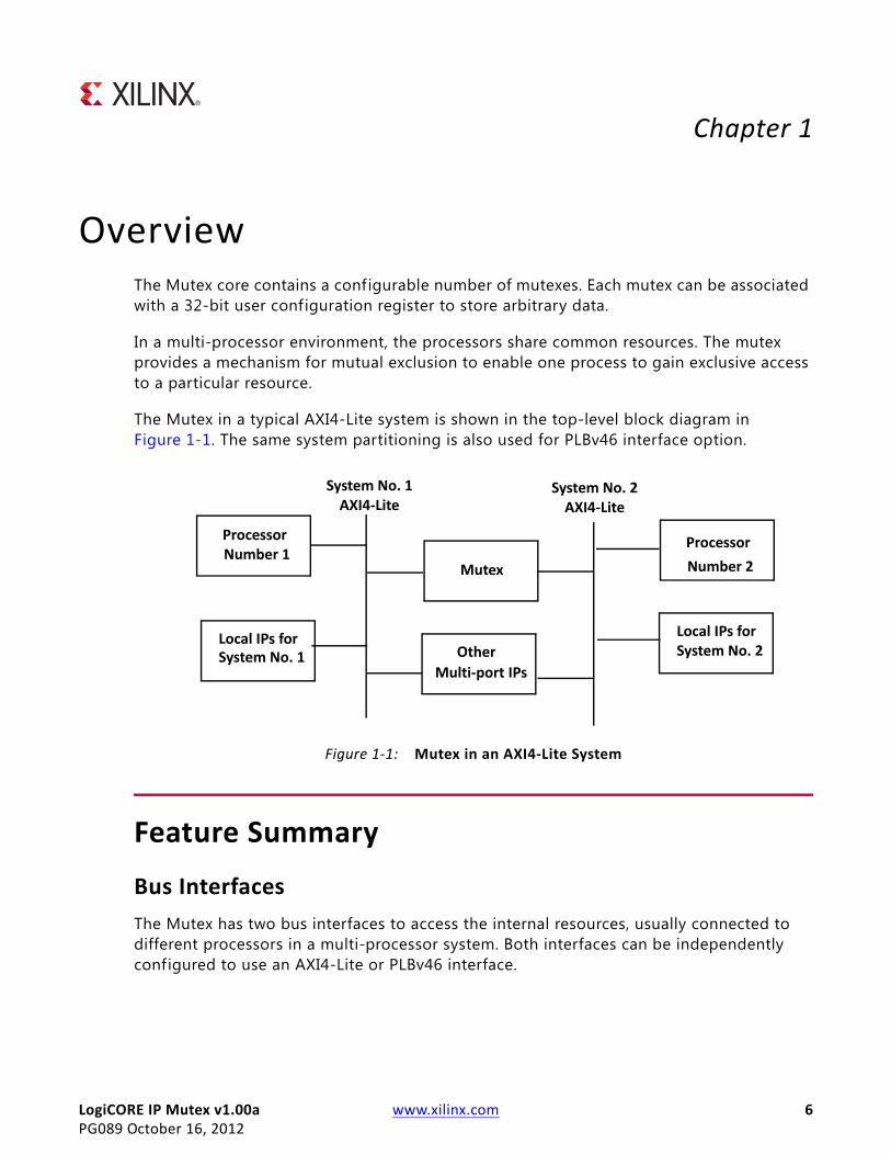
The Mutex in a typical AXI4-Lite system is shown in the top-level block diagram in Figure 1-1. The same system partitioning is also used for PLBv46 interface option.
Feature Summary
Bus InterfacesThe Mutex has two bus interfaces to access the internal resources, usually connected to different processors in a multi-processor system. Both interfaces can be independently configured to use an AXI4-Lite or PLBv46 interface.
X-Ref Target - Figure 1-1
Figure 1-1: Mutex in an AXI4-Lite System
ProcessorNumber 1
Local IPs forSystem No. 1
ProcessorNumber 2
Local IPs forSystem No. 2
Mutex
OtherMulti-port IPs
System No. 1AXI4-Lite
System No. 2AXI4-Lite

LogiCORE IP Mutex v1.00a www.xilinx.com 7PG089 October 16, 2012
Chapter 1: Overview
RegistersThe Mutex provides several types of registers, available with AXI4-Lite and PLBv46 bus interfaces, to lock and release the mutex, and provide a user configuration register:
• Mutex registers, which provides the possibility to lock and release the mutex.
• User configuration.
Protection• The Mutex provides hardware tamper-proof protection of mutex access, preventing any
processor except the intended from modifying a mutex.
Licensing and Ordering InformationThis Xilinx® LogiCORE™ IP module is provided at no additional cost with the Xilinx Vivado™ Design Suite and ISE® Design Suite Embedded Edition tools under the terms of the Xilinx End User License.
Information about this and other Xilinx LogiCORE IP modules is available at the Xilinx Intellectual Property page. For information on pricing and availability of other Xilinx LogiCORE IP modules and tools, contact your local Xilinx sales representative.
LogiCORE IP Mutex v1.00a www.xilinx.com 8PG089 October 16, 2012
Chapter 2
Product Specification
Standards ComplianceThe Mutex adheres to the AXI4-Lite standard defined in the ARM® AMBA® AXI and ACE Protocol Specification [Ref 1].
The Mutex implements a Processor Local Bus slave interface (see IBM 128-Bit Processor Local Bus Architectural Specification (v4.6) [Ref 2]).
PerformanceThe frequency and latency of the Mutex are optimized for use with MicroBlaze™. This means that the frequency targets are aligned to MicroBlaze targets.
Maximum FrequenciesTable 2-1 lists clock frequencies for the target families. The maximum achievable clock frequencycan vary. The maximum achievable clock frequency and all resource counts can be affected by thetool flow, other tool options, additional logic in the FPGA, different versions of the Xilinx tools,and other factors.
Table 2-1: Maximum Frequencies
Architecture Speed grade Max FrequencySpartan®-6 -4 195
Virtex®-6 -3 300
Artix™-7 -3 225
Kintex™-7 -3 320
Virtex-7 -3 320
LogiCORE IP Mutex v1.00a www.xilinx.com 9PG089 October 16, 2012
Chapter 2: Product Specification
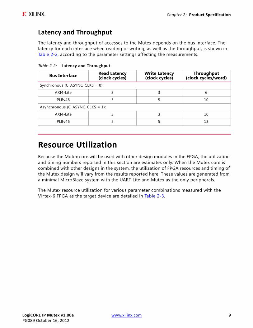
Latency and ThroughputThe latency and throughput of accesses to the Mutex depends on the bus interface. The latency for each interface when reading or writing, as well as the throughput, is shown in Table 2-2, according to the parameter settings affecting the measurements.
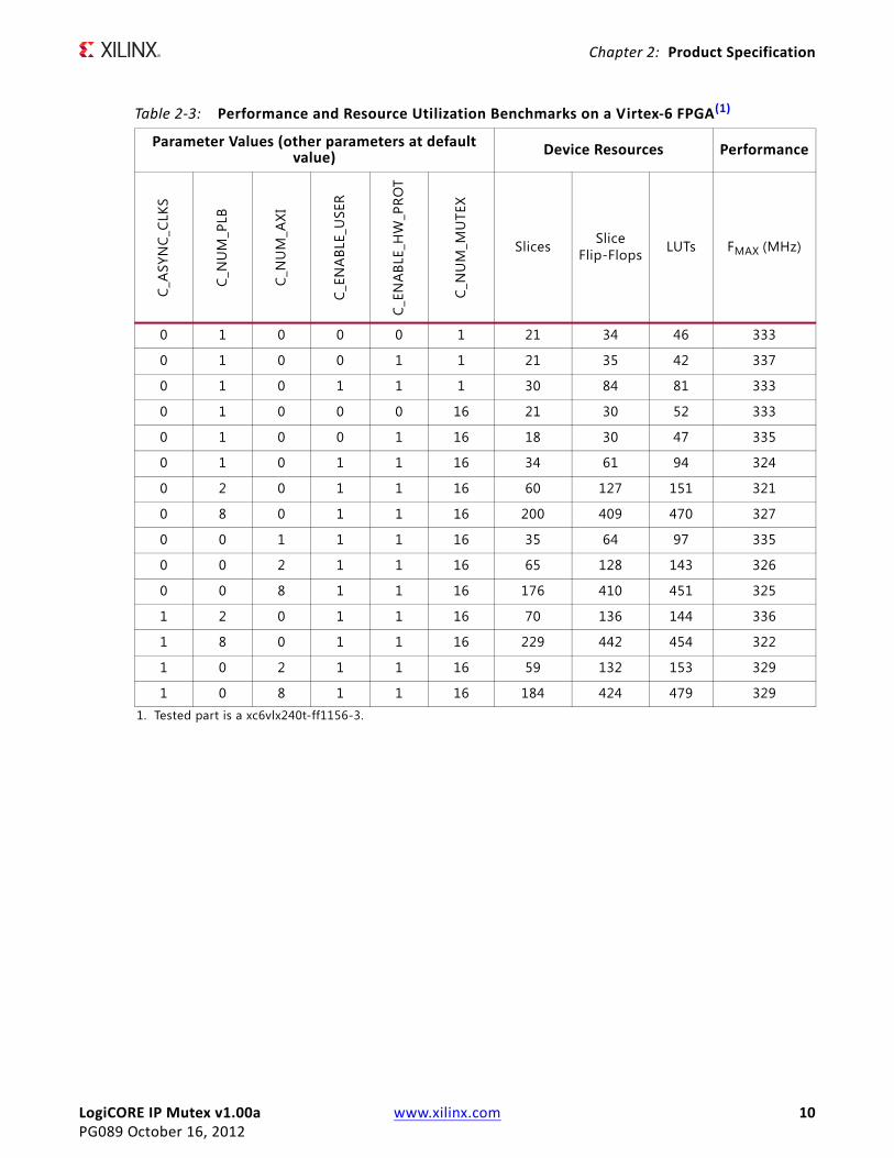
Resource UtilizationBecause the Mutex core will be used with other design modules in the FPGA, the utilization and timing numbers reported in this section are estimates only. When the Mutex core is combined with other designs in the system, the utilization of FPGA resources and timing of the Mutex design will vary from the results reported here. These values are generated from a minimal MicroBlaze system with the UART Lite and Mutex as the only peripherals.
The Mutex resource utilization for various parameter combinations measured with the Virtex-6 FPGA as the target device are detailed in Table 2-3.
Table 2-2: Latency and Throughput
Bus Interface Read Latency(clock cycles)
Write Latency(clock cycles)
Throughput(clock cycles/word)
Synchronous (C_ASYNC_CLKS = 0):
AXI4-Lite 3 3 6
PLBv46 5 5 10
Asynchronous (C_ASYNC_CLKS = 1):
AXI4-Lite 3 3 10
PLBv46 5 5 13
LogiCORE IP Mutex v1.00a www.xilinx.com 10PG089 October 16, 2012
Chapter 2: Product Specification
Table 2-3: Performance and Resource Utilization Benchmarks on a Virtex-6 FPGA(1)
Parameter Values (other parameters at default value) Device Resources Performance
C_A
SYN
C_CL
KS
C_N
UM
_PLB
C_N
UM
_AXI
C_E
NA
BLE_
USE
R
C_EN
ABL
E_H
W_P
ROT
C_N
UM
_MU
TEX
Slices Slice Flip-Flops LUTs FMAX (MHz)
0 1 0 0 0 1 21 34 46 333
0 1 0 0 1 1 21 35 42 337
0 1 0 1 1 1 30 84 81 333
0 1 0 0 0 16 21 30 52 333
0 1 0 0 1 16 18 30 47 335
0 1 0 1 1 16 34 61 94 324
0 2 0 1 1 16 60 127 151 321
0 8 0 1 1 16 200 409 470 327
0 0 1 1 1 16 35 64 97 335
0 0 2 1 1 16 65 128 143 326
0 0 8 1 1 16 176 410 451 325
1 2 0 1 1 16 70 136 144 336
1 8 0 1 1 16 229 442 454 322
1 0 2 1 1 16 59 132 153 329
1 0 8 1 1 16 184 424 479 3291. Tested part is a xc6vlx240t-ff1156-3.
LogiCORE IP Mutex v1.00a www.xilinx.com 11PG089 October 16, 2012
Chapter 2: Product Specification
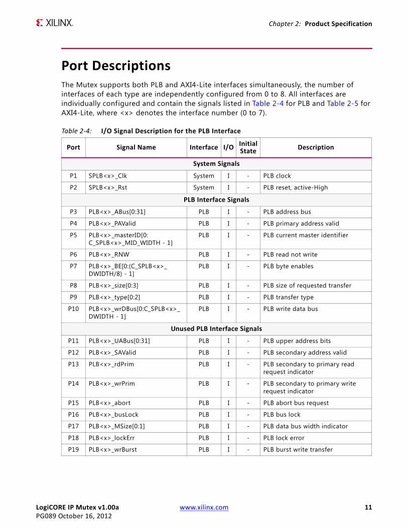
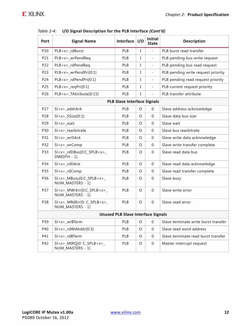
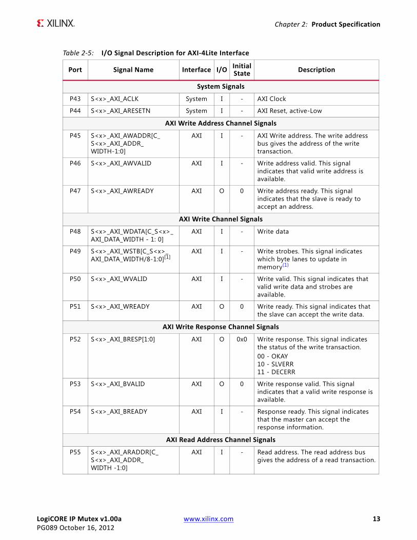
Port DescriptionsThe Mutex supports both PLB and AXI4-Lite interfaces simultaneously, the number of interfaces of each type are independently configured from 0 to 8. All interfaces are individually configured and contain the signals listed in Table 2-4 for PLB and Table 2-5 for AXI4-Lite, where <x> denotes the interface number (0 to 7).
Table 2-4: I/O Signal Description for the PLB Interface
Port Signal Name Interface I/O InitialState Description
System Signals
P1 SPLB<x>_Clk System I - PLB clock
P2 SPLB<x>_Rst System I - PLB reset, active-High
PLB Interface Signals
P3 PLB<x>_ABus[0:31] PLB I - PLB address bus
P4 PLB<x>_PAValid PLB I - PLB primary address valid
P5 PLB<x>_masterID[0: C_SPLB<x>_MID_WIDTH - 1]
PLB I - PLB current master identif ier
P6 PLB<x>_RNW PLB I - PLB read not write
P7 PLB<x>_BE[0:(C_SPLB<x>_DWIDTH/8) - 1]
PLB I - PLB byte enables
P8 PLB<x>_size[0:3] PLB I - PLB size of requested transfer
P9 PLB<x>_type[0:2] PLB I - PLB transfer type
P10 PLB<x>_wrDBus[0:C_SPLB<x>_DWIDTH - 1]
PLB I - PLB write data bus
Unused PLB Interface Signals
P11 PLB<x>_UABus[0:31] PLB I - PLB upper address bits
P12 PLB<x>_SAValid PLB I - PLB secondary address valid
P13 PLB<x>_rdPrim PLB I - PLB secondary to primary read request indicator
P14 PLB<x>_wrPrim PLB I - PLB secondary to primary write request indicator
P15 PLB<x>_abort PLB I - PLB abort bus request
P16 PLB<x>_busLock PLB I - PLB bus lock
P17 PLB<x>_MSize[0:1] PLB I - PLB data bus width indicator
P18 PLB<x>_lockErr PLB I - PLB lock error
P19 PLB<x>_wrBurst PLB I - PLB burst write transfer
LogiCORE IP Mutex v1.00a www.xilinx.com 12PG089 October 16, 2012
Chapter 2: Product Specification
P20 PLB<x>_rdBurst PLB I - PLB burst read transfer
P21 PLB<x>_wrPendReq PLB I - PLB pending bus write request
P22 PLB<x>_rdPendReq PLB I - PLB pending bus read request
P23 PLB<x>_wrPendPri[0:1] PLB I - PLB pending write request priority
P24 PLB<x>_rdPendPri[0:1] PLB I - PLB pending read request priority
P25 PLB<x>_reqPri[0:1] PLB I - PLB current request priority
P26 PLB<x>_TAttribute[0:15] PLB I - PLB transfer attribute
PLB Slave Interface Signals
P27 Sl<x>_addrAck PLB O 0 Slave address acknowledge
P28 Sl<x>_SSize[0:1] PLB O 0 Slave data bus size
P29 Sl<x>_wait PLB O 0 Slave wait
P30 Sl<x>_rearbitrate PLB O 0 Slave bus rearbitrate
P31 Sl<x>_wrDAck PLB O 0 Slave write data acknowledge
P32 Sl<x>_wrComp PLB O 0 Slave write transfer complete
P33 Sl<x>_rdDBus[0:C_SPLB<x>_DWIDTH - 1]
PLB O 0 Slave read data bus
P34 Sl<x>_rdDAck PLB O 0 Slave read data acknowledge
P35 Sl<x>_rdComp PLB O 0 Slave read transfer complete
P36 Sl<x>_MBusy[0:C_SPLB<x>_NUM_MASTERS - 1]
PLB O 0 Slave busy
P37 Sl<x>_MWrErr[0:C_SPLB<x>_NUM_MASTERS - 1]
PLB O 0 Slave write error
P38 Sl<x>_MRdErr[0: C_SPLB<x>_NUM_MASTERS - 1]
PLB O 0 Slave read error
Unused PLB Slave Interface Signals
P39 Sl<x>_wrBTerm PLB O 0 Slave terminate write burst transfer
P40 Sl<x>_rdWdAddr[0:3] PLB O 0 Slave read word address
P41 Sl<x>_rdBTerm PLB O 0 Slave terminate read burst transfer
P42 Sl<x>_MIRQ[0: C_SPLB<x>_NUM_MASTERS - 1]
PLB O 0 Master interrupt request
Table 2-4: I/O Signal Description for the PLB Interface (Cont’d)
Port Signal Name Interface I/O InitialState Description
LogiCORE IP Mutex v1.00a www.xilinx.com 13PG089 October 16, 2012
Chapter 2: Product Specification
Table 2-5: I/O Signal Description for AXI-4Lite Interface
Port Signal Name Interface I/O InitialState Description
System Signals
P43 S<x>_AXI_ACLK System I - AXI Clock
P44 S<x>_AXI_ARESETN System I - AXI Reset, active-Low
AXI Write Address Channel Signals
P45 S<x>_AXI_AWADDR[C_S<x>_AXI_ADDR_WIDTH-1:0]
AXI I - AXI Write address. The write address bus gives the address of the write transaction.
P46 S<x>_AXI_AWVALID AXI I - Write address valid. This signal indicates that valid write address is available.
P47 S<x>_AXI_AWREADY AXI O 0 Write address ready. This signal indicates that the slave is ready to accept an address.
AXI Write Channel Signals
P48 S<x>_AXI_WDATA[C_S<x>_AXI_DATA_WIDTH - 1: 0]
AXI I - Write data
P49 S<x>_AXI_WSTB[C_S<x>_AXI_DATA_WIDTH/8-1:0][1]
AXI I - Write strobes. This signal indicates which byte lanes to update in memory(1)
P50 S<x>_AXI_WVALID AXI I - Write valid. This signal indicates that valid write data and strobes are available.
P51 S<x>_AXI_WREADY AXI O 0 Write ready. This signal indicates that the slave can accept the write data.
AXI Write Response Channel Signals
P52 S<x>_AXI_BRESP[1:0] AXI O 0x0 Write response. This signal indicates the status of the write transaction.00 - OKAY10 - SLVERR11 - DECERR
P53 S<x>_AXI_BVALID AXI O 0 Write response valid. This signal indicates that a valid write response is available.
P54 S<x>_AXI_BREADY AXI I - Response ready. This signal indicates that the master can accept the response information.
AXI Read Address Channel Signals
P55 S<x>_AXI_ARADDR[C_S<x>_AXI_ADDR_WIDTH -1:0]
AXI I - Read address. The read address bus gives the address of a read transaction.

LogiCORE IP Mutex v1.00a www.xilinx.com 14PG089 October 16, 2012
Chapter 2: Product Specification
Register SpaceEach interface of the Mutex core can access all mutexes. Only one interface at the time can access any of the mutexes. For example, while one interface is accessing any of the mutexes, all other PLB and AXI interfaces are blocked. Interface arbitration has fixed priority where PLB 0-7 has higher priority than AXI 0-7 in descending order. For example, PLB0 has the highest priority, and S7_AXI the lowest. Table 2-6 shows all the Mutex registers and their addresses offsets.
P56 S<x>_AXI_ARVALID AXI I - Read address valid. This signal indicates, when HIGH, that the read address is valid and will remain stable until the address acknowledge signal, S<x>_AXI_ARREADY, is High.
P57 S<x>_AXI_ARREADY AXI O 1 Read address ready. This signal indicates that the slave is ready to accept an address.
AXI Read Data Channel Signals
P58 S<x>_AXI_RDATA[C_S<x>_AXI_DATA_WIDTH -1:0]
AXI O 0x0 Read data
P59 S<x>_AXI_RRESP[1:0] AXI O 0x0 Read response. This signal indicates the status of the read transfer.00 - OKAY10 - SLVERR11 - DECERR
P60 S<x>_AXI_RVALID AXI O 0 Read valid. This signal indicates that the required read data is available and the read transfer can complete
P61 S<x>_AXI_RREADY AXI I - Read ready. This signal indicates that the master can accept the read data and response information
1. This signal is not used. The Mutex assumes that all byte lanes are active.
Table 2-6: Mutex Registers
Base Address +Offset (hex)
RegisterName
AccessType
DefaultValue (hex) Description
BASEADDR + 0x0 MUTEX R/W 0 Mutex register for mutex ownership
BASEADDR + 0x4 USER N/A 0 USER configuration register.
BASEADDR + 0x8 to 0xFC Reserved Reserved for future use
Table 2-5: I/O Signal Description for AXI-4Lite Interface (Cont’d)
Port Signal Name Interface I/O InitialState Description
LogiCORE IP Mutex v1.00a www.xilinx.com 15PG089 October 16, 2012
Chapter 2: Product Specification
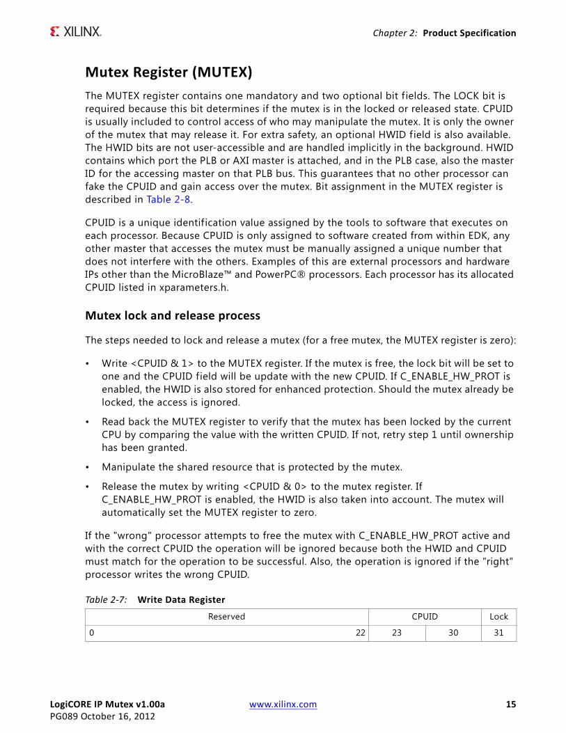
Mutex Register (MUTEX)The MUTEX register contains one mandatory and two optional bit f ields. The LOCK bit is required because this bit determines if the mutex is in the locked or released state. CPUID is usually included to control access of who may manipulate the mutex. It is only the owner of the mutex that may release it. For extra safety, an optional HWID field is also available. The HWID bits are not user-accessible and are handled implicitly in the background. HWID contains which port the PLB or AXI master is attached, and in the PLB case, also the master ID for the accessing master on that PLB bus. This guarantees that no other processor can fake the CPUID and gain access over the mutex. Bit assignment in the MUTEX register is described in Table 2-8.
CPUID is a unique identif ication value assigned by the tools to software that executes on each processor. Because CPUID is only assigned to software created from within EDK, any other master that accesses the mutex must be manually assigned a unique number that does not interfere with the others. Examples of this are external processors and hardware IPs other than the MicroBlaze™ and PowerPC® processors. Each processor has its allocated CPUID listed in xparameters.h.
Mutex lock and release process
The steps needed to lock and release a mutex (for a free mutex, the MUTEX register is zero):
• Write <CPUID & 1> to the MUTEX register. If the mutex is free, the lock bit will be set to one and the CPUID field will be update with the new CPUID. If C_ENABLE_HW_PROT is enabled, the HWID is also stored for enhanced protection. Should the mutex already be locked, the access is ignored.
• Read back the MUTEX register to verify that the mutex has been locked by the current CPU by comparing the value with the written CPUID. If not, retry step 1 until ownership has been granted.
• Manipulate the shared resource that is protected by the mutex.
• Release the mutex by writing <CPUID & 0> to the mutex register. If C_ENABLE_HW_PROT is enabled, the HWID is also taken into account. The mutex will automatically set the MUTEX register to zero.
If the "wrong" processor attempts to free the mutex with C_ENABLE_HW_PROT active and with the correct CPUID the operation will be ignored because both the HWID and CPUID must match for the operation to be successful. Also, the operation is ignored if the "right" processor writes the wrong CPUID.
Table 2-7: Write Data Register
Reserved CPUID Lock
0 22 23 30 31

LogiCORE IP Mutex v1.00a www.xilinx.com 16PG089 October 16, 2012
Chapter 2: Product Specification
Mutex User Configuration Register (USER)The USER configuration is used to store a 32-bit value associated with a mutex. It can contain any arbitrary information. Bit assignment in the USER register is described in Table 2-10.
Table 2-8: Write Data Register Bit Definitions
Bit(s) Name CoreAccess
ResetValue Description
0 - 22 Reserved N/A 0 Reserved for future use.
23 - 30 CPUID R/W - Unique processor ID number.
31 LOCK R/W - Lock status: 0 = free, 1 = Mutex currently owned by CPUID.
Table 2-9: User Configuration Register (USER)
USER
0 31
Table 2-10: Mutex Read Data Register Bit Definitions
Bit(s) Name Core Access Reset Value Description
0 - 31 USER R/W - User configuration register

LogiCORE IP Mutex v1.00a www.xilinx.com 17PG089 October 16, 2012
Chapter 3
Designing with the Core
General Design GuidelinesThis chapter includes guidelines and additional information to facilitate designing with the core.
ClockingThe SPLBn_Clk (n = 0 - 7) input is only used when the PLBv46 bus is used. Then it should normally be connected to the same clock as the bus.
The Sn_AXI_ACLK (n = 0 - 7) input is only used when the AXI4-Lite interconnect is used. Then it should normally be connected to the same clock as the interconnect.
With synchronous operation (C_ASYNC_CLKS = 0), the clock inputs used must all be connected to the same clock signal in all the above cases.
ResetsThe SPLBn_Rst (n = 0 - 7) input is only used when the PLBv46 bus is used. Then it should normally be connected to the same reset as the bus.
The Sn_AXI_ARESETN (n = 0 - 7) input is only used when the AXI4-Lite interconnect is used. Then it should normally be connected to the same reset as the interconnect.

LogiCORE IP Mutex v1.00a www.xilinx.com 18PG089 October 16, 2012
Chapter 3: Designing with the Core
Protocol DescriptionSee the AMBA® AXI4 Interface standard for a description of the AXI4-Lite protocol (ARM® AMBA AXI and ACE Protocol Specification, Version 2.0 ARM IHI 0022D [Ref 1]).
See the Processor Local Bus slave interface standard for a description of the PLBv46 protocol (IBM 128-Bit Processor Local Bus Architectural Specification (v4.6) [Ref 2]).
LogiCORE IP Mutex v1.00a www.xilinx.com 19PG089 October 16, 2012
SECTION II: VIVADO DESIGN SUITE
Customizing and Generating the Core
Constraining the Core
LogiCORE IP Mutex v1.00a www.xilinx.com 20PG089 October 16, 2012
Chapter 4
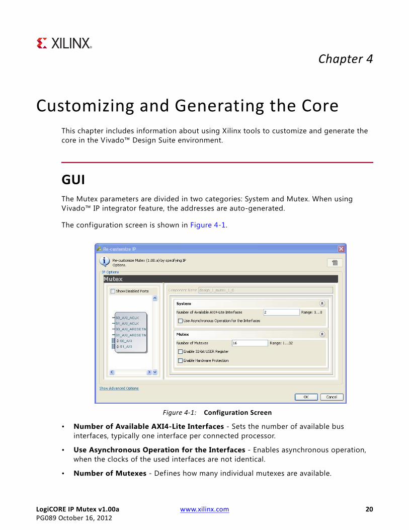
Customizing and Generating the CoreThis chapter includes information about using Xilinx tools to customize and generate the core in the Vivado™ Design Suite environment.
GUIThe Mutex parameters are divided in two categories: System and Mutex. When using Vivado™ IP integrator feature, the addresses are auto-generated.
The configuration screen is shown in Figure 4-1.
• Number of Available AXI4-Lite Interfaces - Sets the number of available bus interfaces, typically one interface per connected processor.
• Use Asynchronous Operation for the Interfaces - Enables asynchronous operation, when the clocks of the used interfaces are not identical.
• Number of Mutexes - Defines how many individual mutexes are available.
X-Ref Target - Figure 4-1
Figure 4-1: Configuration Screen

LogiCORE IP Mutex v1.00a www.xilinx.com 21PG089 October 16, 2012
Chapter 4: Customizing and Generating the Core
• Enable 32-bit USER Register - The USER register can be used to store arbitrary data. Usually it stores the address to the shared resource controlled by the mutex.
• Enable Hardware Protection - When hardware protection is enabled, HWID is used to complement the CPUID for enhanced security. The HWID consists of the AXI interface number and AXI transaction ID for the processor that has locked the mutex. The HWID is not user-accessible and is thus tamper proof.
GUI ParametersThe Mutex design is parameterized to tailor it for different systems. This allows you to configure a design that uses the resources required by the system only and that operates with the best possible performance. The features that can be parameterized in the Mutex design are shown in Table 4-1.
Table 4-1: Design Parameters
Generic Feature/Description Parameter Name AllowableValues
DefaultValue
VHDLType
System Parameter
G1 Target FPGA family C_FAMILY Supportedarchitectures
virtex7 string
Mutex Parameters
G17 Specify if interfaces are synchronous or asynchronous
C_ASYNC_CLKS 0 - 1 0 Integer
G19 Number of AXI4-Lite interfaces C_NUM_AXI 0 - 8 0 Integer
G20 If the 32-bit USER register associated with a mutex should be available
C_ENABLE_USER 0 - 1 32 Integer
G21 Number of bits used for the CPUID field
C_OWNER_ID_WIDTH 8 8 Integer
G22 If hardware protection of a mutex should be enabled besides the CPUID (if available)
C_ENABLE_HW_PROT 0 - 1 0 Integer
G23 Number of mutexes that are contained inside the core
C_NUM_MUTEX 1 - 32 16 Integer
Shortened Title with Core Version www.xilinx.com 22PG000 August 10, 2012
Chapter 5
Constraining the CoreThis chapter contains information about constraining the core in the Vivado™ Design Suite environment.
Required ConstraintsThere are no required constraints for this core.
Device, Package, and Speed Grade SelectionsThere are no Device, Package or Speed Grade requirements for this core.
Clock FrequenciesThere are no specific clock frequency requirements for this core.
Clock ManagementThe Mutex can either be fully synchronous with all clocked elements clocked by the same physical clock, or asynchronous with different clocks on the connected bus interfaces.
With an asynchronous configuration, the parameter C_ASYNC_CLKS (Use Asynchronous Operation for the Interfaces) must be set manually.
To operate properly when connected to MicroBlaze™, the corresponding bus interface clock must be the same as the MicroBlaze Clk .

Shortened Title with Core Version www.xilinx.com 23PG000 August 10, 2012
Chapter 5: Constraining the Core
Clock PlacementThere are no specific Clock placement requirements for this core.
BankingThere are no specific Banking rules for this core.
Transceiver PlacementThere are no Transceiver Placement requirements for this core.
I/O Standard and PlacementThere are no specific I/O standards and placement requirements for this core.

LogiCORE IP Mutex v1.00a www.xilinx.com 24PG089 October 16, 2012
SECTION III: ISE DESIGN SUITE
Customizing and Generating the Core
Constraining the Core
LogiCORE IP Mutex v1.00a www.xilinx.com 25PG089 October 16, 2012
Chapter 6
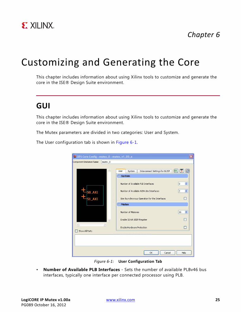
Customizing and Generating the CoreThis chapter includes information about using Xilinx tools to customize and generate the core in the ISE® Design Suite environment.
GUIThis chapter includes information about using Xilinx tools to customize and generate the core in the ISE® Design Suite environment.
The Mutex parameters are divided in two categories: User and System.
The User configuration tab is shown in Figure 6-1.
• Number of Available PLB Interfaces - Sets the number of available PLBv46 bus interfaces, typically one interface per connected processor using PLB.
X-Ref Target - Figure 6-1
Figure 6-1: User Configuration Tab

LogiCORE IP Mutex v1.00a www.xilinx.com 26PG089 October 16, 2012
Chapter 6: Customizing and Generating the Core
• Number of Available AXI4-Lite Interfaces - Sets the number of available AXI4-Lite bus interfaces, typically one interface per connected processor using AXI.
• Use Asynchronous Operation for the Interfaces - Enables asynchronous operation, when the clocks of the used interfaces are not identical.
• Number of Mutexes - Defines how many individual mutexes are available.
• Enable 32-bit USER Register - The USER register can be used to store arbitrary data. Usually it stores the address to the shared resource controlled by the mutex.
• Enable Hardware Protection - When hardware protection is enabled, HWID is used to complement the CPUID for enhanced security. The HWID consists of the AXI interface number and AXI transaction ID for the processor that has locked the mutex. The HWID is not user-accessible and is thus tamper proof.
The System configuration tab is shown in Figure 6-1.
• Base Address - The base address of each bus interface in use, AXI4-Lite or PLBv46.
• High Address - The high address of each bus interface in use, AXI4-Lite or PLBv46.
X-Ref Target - Figure 6-2
Figure 6-2: System Configuration Tab
LogiCORE IP Mutex v1.00a www.xilinx.com 27PG089 October 16, 2012
Chapter 6: Customizing and Generating the Core
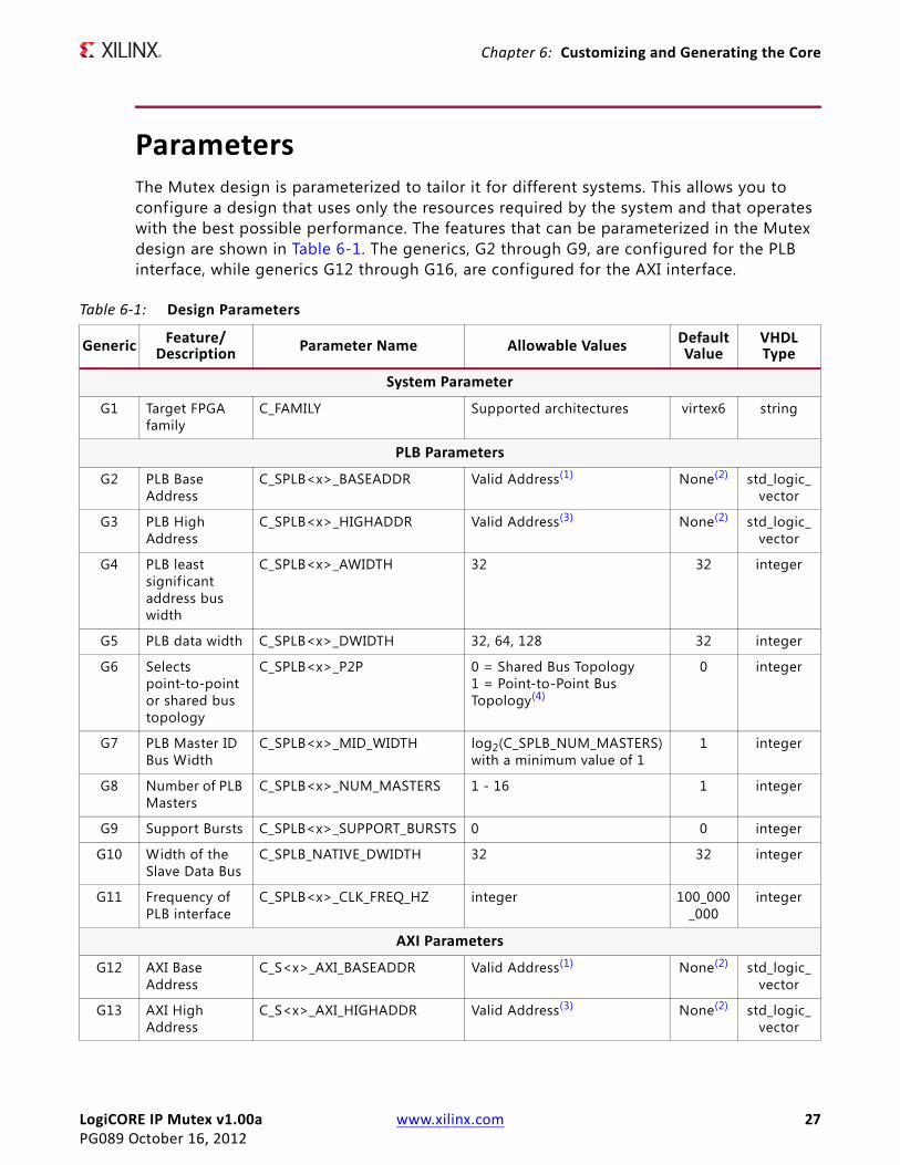
ParametersThe Mutex design is parameterized to tailor it for different systems. This allows you to configure a design that uses only the resources required by the system and that operates with the best possible performance. The features that can be parameterized in the Mutex design are shown in Table 6-1. The generics, G2 through G9, are configured for the PLB interface, while generics G12 through G16, are configured for the AXI interface.
Table 6-1: Design Parameters
Generic Feature/Description Parameter Name Allowable Values Default
ValueVHDLType
System Parameter
G1 Target FPGA family
C_FAMILY Supported architectures virtex6 string
PLB Parameters
G2 PLB Base Address
C_SPLB<x>_BASEADDR Valid Address(1) None(2) std_logic_vector
G3 PLB High Address
C_SPLB<x>_HIGHADDR Valid Address(3) None(2) std_logic_vector
G4 PLB least signif icant address bus width
C_SPLB<x>_AWIDTH 32 32 integer
G5 PLB data width C_SPLB<x>_DWIDTH 32, 64, 128 32 integer
G6 Selects point-to-point or shared bus topology
C_SPLB<x>_P2P 0 = Shared Bus Topology1 = Point-to-Point Bus Topology(4)
0 integer
G7 PLB Master ID Bus Width
C_SPLB<x>_MID_WIDTH log2(C_SPLB_NUM_MASTERS) with a minimum value of 1
1 integer
G8 Number of PLB Masters
C_SPLB<x>_NUM_MASTERS 1 - 16 1 integer
G9 Support Bursts C_SPLB<x>_SUPPORT_BURSTS 0 0 integer
G10 Width of the Slave Data Bus
C_SPLB_NATIVE_DWIDTH 32 32 integer
G11 Frequency of PLB interface
C_SPLB<x>_CLK_FREQ_HZ integer 100_000_000
integer
AXI Parameters
G12 AXI Base Address
C_S<x>_AXI_BASEADDR Valid Address(1) None(2) std_logic_vector
G13 AXI High Address
C_S<x>_AXI_HIGHADDR Valid Address(3) None(2) std_logic_vector

LogiCORE IP Mutex v1.00a www.xilinx.com 28PG089 October 16, 2012
Chapter 6: Customizing and Generating the Core
G14 AXI address bus width
C_S<x>_AXI_ADDR_WIDTH 32 32 integer
G15 AXI data bus width
C_S<x>_AXI_DATA_WIDTH 32 32 integer
G16 AXI interface type
C_S<x>_AXI_PROTOCOL AXI4LITE AXI4LITE
string
Mutex Parameters
G17 Specify if interfaces are synchronous or asynchronous
C_ASYNC_CLKS 0 - 1 0 Integer
G18 Number of PLB interfaces
C_NUM_PLB 0 - 8 2 Integer
G19 Number of AXI4-Lite interfaces
C_NUM_AXI 0 - 8 0 Integer
G20 If the 32-bit USER register associated with a mutex should be available
C_ENABLE_USER 0 - 1 32 Integer
G21 Number of bits used for the CPUID f ield
C_OWNER_ID_WIDTH 8 8 Integer
G22 If hardware protection of a mutex should be enabled besides the CPUID (if available)
C_ENABLE_HW_PROT 0 - 1 0 Integer
G23 Number of mutexes that are contained inside the core
C_NUM_MUTEX 1 - 32 16 Integer
Notes: 1. The user must set the values. The C_<interface>_BASEADDR must be a multiple of the range, where the range is
C_<interface>_HIGHADDR - C_<interface>_BASEADDR + 12. No default value will be specif ied to insure that the actual value is set, i.e., if the value is not set, a compiler error will be
generated.3. C_<interface>_HIGHADDR - C_<interface>_BASEADDR must be a power of 2 greater than equal to
C_<interface>_BASEADDR + 0xFF.4. Value of 1 is not supported in this core.
Table 6-1: Design Parameters (Cont’d)
Generic Feature/Description Parameter Name Allowable Values Default
ValueVHDLType
LogiCORE IP Mutex v1.00a www.xilinx.com 29PG089 October 16, 2012
Chapter 6: Customizing and Generating the Core
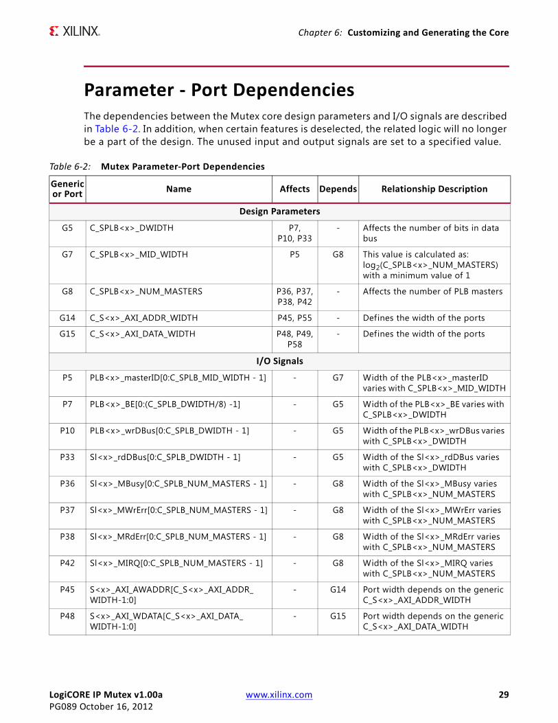
Parameter - Port DependenciesThe dependencies between the Mutex core design parameters and I/O signals are described in Table 6-2. In addition, when certain features is deselected, the related logic will no longer be a part of the design. The unused input and output signals are set to a specif ied value.
Table 6-2: Mutex Parameter-Port Dependencies
Genericor Port Name Affects Depends Relationship Description
Design Parameters
G5 C_SPLB<x>_DWIDTH P7, P10, P33
- Affects the number of bits in data bus
G7 C_SPLB<x>_MID_WIDTH P5 G8 This value is calculated as:log2(C_SPLB<x>_NUM_MASTERS)with a minimum value of 1
G8 C_SPLB<x>_NUM_MASTERS P36, P37,P38, P42
- Affects the number of PLB masters
G14 C_S<x>_AXI_ADDR_WIDTH P45, P55 - Defines the width of the ports
G15 C_S<x>_AXI_DATA_WIDTH P48, P49,P58
- Defines the width of the ports
I/O Signals
P5 PLB<x>_masterID[0:C_SPLB_MID_WIDTH - 1] - G7 Width of the PLB<x>_masterIDvaries with C_SPLB<x>_MID_WIDTH
P7 PLB<x>_BE[0:(C_SPLB_DWIDTH/8) -1] - G5 Width of the PLB<x>_BE varies with C_SPLB<x>_DWIDTH
P10 PLB<x>_wrDBus[0:C_SPLB_DWIDTH - 1] - G5 Width of the PLB<x>_wrDBus varies with C_SPLB<x>_DWIDTH
P33 Sl<x>_rdDBus[0:C_SPLB_DWIDTH - 1] - G5 Width of the Sl<x>_rdDBus varies with C_SPLB<x>_DWIDTH
P36 Sl<x>_MBusy[0:C_SPLB_NUM_MASTERS - 1] - G8 Width of the Sl<x>_MBusy varies with C_SPLB<x>_NUM_MASTERS
P37 Sl<x>_MWrErr[0:C_SPLB_NUM_MASTERS - 1] - G8 Width of the Sl<x>_MWrErr varies with C_SPLB<x>_NUM_MASTERS
P38 Sl<x>_MRdErr[0:C_SPLB_NUM_MASTERS - 1] - G8 Width of the Sl<x>_MRdErr varies with C_SPLB<x>_NUM_MASTERS
P42 Sl<x>_MIRQ[0:C_SPLB_NUM_MASTERS - 1] - G8 Width of the Sl<x>_MIRQ varies with C_SPLB<x>_NUM_MASTERS
P45 S<x>_AXI_AWADDR[C_S<x>_AXI_ADDR_WIDTH-1:0]
- G14 Port width depends on the generic C_S<x>_AXI_ADDR_WIDTH
P48 S<x>_AXI_WDATA[C_S<x>_AXI_DATA_WIDTH-1:0]
- G15 Port width depends on the generic C_S<x>_AXI_DATA_WIDTH

LogiCORE IP Mutex v1.00a www.xilinx.com 30PG089 October 16, 2012
Chapter 6: Customizing and Generating the Core
P49 S<x>_AXI_WSTB[C_S<x>_AXI_DATA_WIDTH/8-1:0]
- G15 Port width depends on the generic C_S<x>_AXI_DATA_WIDTH
P55 S<x>_AXI_ARADDR[C_S<x>_AXI_ADDR_WIDTH -1:0]
- G14 Port width depends on the generic C_S<x>_AXI_ADDR_WIDTH
P58 S<x>_AXI_RDATA[C_S<x>_AXI_DATA_WIDTH -1:0]
- G15 Port width depends on the generic C_S<x>_AXI_DATA_WIDTH
Table 6-2: Mutex Parameter-Port Dependencies (Cont’d)
Genericor Port Name Affects Depends Relationship Description
LogiCORE IP Mutex v1.00a www.xilinx.com 31PG089 October 16, 2012
Chapter 7
Constraining the CoreThis chapter contains information about constraining the core in the ISE® Design Suite environment.
Required ConstraintsThere are no required constraints for this core.
Device, Package, and Speed Grade SelectionsThere are no Device, Package or Speed Grade requirements for this core.
Clock FrequenciesThere are no specific clock frequency requirements for this core.
Clock ManagementThe Mutex can either be fully synchronous with all clocked elements clocked by the same physical clock, or asynchronous with different clocks on the connected bus interfaces.
With an asynchronous configuration, the parameter C_ASYNC_CLKS (Use Asynchronous Operation for the Interfaces) must be set manually.
To operate properly when connected to MicroBlaze™, the corresponding bus interface clock must be the same as the MicroBlaze Clk .
LogiCORE IP Mutex v1.00a www.xilinx.com 32PG089 October 16, 2012
Chapter 7: Constraining the Core
Clock PlacementThere are no specific Clock placement requirements for this core.
BankingThere are no specific Banking rules for this core.
Transceiver PlacementThere are no Transceiver Placement requirements for this core.
I/O Standard and PlacementThere are no specific I/O standards and placement requirements for this core.

LogiCORE IP Mutex v1.00a www.xilinx.com 33PG089 October 16, 2012
SECTION IV: APPENDICES
Migrating
Debugging
Application Software Development
Additional Resources

LogiCORE IP Mutex v1.00a www.xilinx.com 34PG089 October 16, 2012
Appendix A
MigratingThis appendix describes migrating from older versions of the IP to the current IP release.
For information on migrating to the Vivado™ Design Suite, see the Vivado Design Suite Migration Methodology Guide [Ref 4].

LogiCORE IP Mutex v1.00a www.xilinx.com 35PG089 October 16, 2012
Appendix B
Debugging
Solution CentersSee the Xilinx Solution Centers for support on devices, software tools, and intellectual property at all stages of the design cycle. Topics include design assistance, advisories, and troubleshooting tips.

LogiCORE IP Mutex v1.00a www.xilinx.com 36PG089 October 16, 2012
Appendix C
Application Software Development
Device DriversThe Mailbox is supported by the mutex driver, included with Xilinx Software Development Kit.

LogiCORE IP Mutex v1.00a www.xilinx.com 37PG089 October 16, 2012
Appendix D
Additional Resources
Xilinx ResourcesFor support resources such as Answers, Documentation, Downloads, and Forums, see the Xilinx Support website at:
www.xilinx.com/support.
For a glossary of technical terms used in Xilinx documentation, see:
www.xilinx.com/company/terms.htm.
ReferencesThese documents provide supplemental material useful with this product guide:
1. ARM® AMBA® AXI and ACE Protocol Specif ication (IHI 0022D)
2. IBM CoreConnect128-Bit Processor Local Bus, Architectural Specification (v4.6)
3. Vivado™ Design Suite user documentation
4. Vivado Design Suite Migration Methodology Guide (UG911)
Technical SupportXilinx provides technical support at www.xilinx.com/support for this LogiCORE™ IP product when used as described in the product documentation. Xilinx cannot guarantee timing, functionality, or support of product if implemented in devices that are not defined in the documentation, if customized beyond that allowed in the product documentation, or if changes are made to any section of the design labeled DO NOT MODIFY.
See the Embedded Edition Derivative Device Support web page (www.xilinx.com/ise/embedded/ddsupport.htm) for a complete list of supported derivative devices for this core.

LogiCORE IP Mutex v1.00a www.xilinx.com 38PG089 October 16, 2012
Appendix D: Additional Resources
Revision HistoryThe following table shows the revision history for this document.
Notice of DisclaimerThe information disclosed to you hereunder (the “Materials”) is provided solely for the selection and use of Xilinx products. To the maximum extent permitted by applicable law: (1) Materials are made available “AS IS” and with all faults, Xilinx hereby DISCLAIMS ALL WARRANTIES AND CONDITIONS, EXPRESS, IMPLIED, OR STATUTORY, INCLUDING BUT NOT LIMITED TO WARRANTIES OF MERCHANTABILITY, NON-INFRINGEMENT, OR FITNESS FOR ANY PARTICULAR PURPOSE; and (2) Xilinx shall not be liable (whether in contract or tort, including negligence, or under any other theory of liability) for any loss or damage of any kind or nature related to, arising under, or in connection with, the Materials (including your use of the Materials), including for any direct, indirect, special, incidental, or consequential loss or damage (including loss of data, profits, goodwill, or any type of loss or damage suffered as a result of any action brought by a third party) even if such damage or loss was reasonably foreseeable or Xilinx had been advised of the possibility of the same. Xilinx assumes no obligation to correct any errors contained in the Materials or to notify you of updates to the Materials or to product specifications. You may not reproduce, modify, distribute, or publicly display the Materials without prior written consent. Certain products are subject to the terms and conditions of the Limited Warranties which can be viewed at http://www.xilinx.com/warranty.htm; IP cores may be subject to warranty and support terms contained in a license issued to you by Xilinx. Xilinx products are not designed or intended to be fail-safe or for use in any application requiring fail-safe performance; you assume sole risk and liability for use of Xilinx products in Critical Applications: http://www.xilinx.com/warranty.htm#critapps.© Copyright 2012 Xilinx, Inc. Xilinx, the Xilinx logo, Artix, ISE, Kintex, Spartan, Virtex, Vivado, Zynq, and other designated brands included herein are trademarks of Xilinx in the United States and other countries. All other trademarks are the property of their respective owners.
Date Version Revision
10/16/12 1.0 Initial Xilinx release. This Product Guide is derived from DS775. Added Vivado support for 2012.3.