LogiCORE IP Defective Pixel Correction v7 Pixel Correction v7.0 4 PG005 December 18, 2013 Product...
62
LogiCORE IP Defective Pixel Correction v7.0 Product Guide for Vivado Design Suite PG005 December 18, 2013 Discontinued IP
-
Upload
truongdien -
Category
Documents
-
view
234 -
download
2
Transcript of LogiCORE IP Defective Pixel Correction v7 Pixel Correction v7.0 4 PG005 December 18, 2013 Product...
LogiCORE IP Defective Pixel Correction v7.0Product Guide for Vivado Design Suite
PG005 December 18, 2013
Discontinued IP

Defective Pixel Correction v7.0 www.xilinx.com 2PG005 December 18, 2013
Table of ContentsIP Facts
Chapter 1: OverviewFeature Summary. . . . . . . . . . . . . . . . . . . . . . . . . . . . . . . . . . . . . . . . . . . . . . . . . . . . . . . . . . . . . . . . . . 5Applications . . . . . . . . . . . . . . . . . . . . . . . . . . . . . . . . . . . . . . . . . . . . . . . . . . . . . . . . . . . . . . . . . . . . . . 6Licensing and Ordering Information . . . . . . . . . . . . . . . . . . . . . . . . . . . . . . . . . . . . . . . . . . . . . . . . . . . 6
Chapter 2: Product SpecificationStandards . . . . . . . . . . . . . . . . . . . . . . . . . . . . . . . . . . . . . . . . . . . . . . . . . . . . . . . . . . . . . . . . . . . . . . . . 7Performance. . . . . . . . . . . . . . . . . . . . . . . . . . . . . . . . . . . . . . . . . . . . . . . . . . . . . . . . . . . . . . . . . . . . . . 7Resource Utilization. . . . . . . . . . . . . . . . . . . . . . . . . . . . . . . . . . . . . . . . . . . . . . . . . . . . . . . . . . . . . . . . 8Core Interfaces and Register Space . . . . . . . . . . . . . . . . . . . . . . . . . . . . . . . . . . . . . . . . . . . . . . . . . . . 9
Chapter 3: Designing with the CoreGeneral Design Guidelines . . . . . . . . . . . . . . . . . . . . . . . . . . . . . . . . . . . . . . . . . . . . . . . . . . . . . . . . . 23Clock, Enable, and Reset Considerations . . . . . . . . . . . . . . . . . . . . . . . . . . . . . . . . . . . . . . . . . . . . . . 24System Considerations . . . . . . . . . . . . . . . . . . . . . . . . . . . . . . . . . . . . . . . . . . . . . . . . . . . . . . . . . . . . 26
Chapter 4: Customizing and Generating the CoreVivado Integrated Design Environment (IDE) . . . . . . . . . . . . . . . . . . . . . . . . . . . . . . . . . . . . . . . . . . 28Interface . . . . . . . . . . . . . . . . . . . . . . . . . . . . . . . . . . . . . . . . . . . . . . . . . . . . . . . . . . . . . . . . . . . . . . . . 28
Chapter 5: Constraining the CoreRequired Constraints . . . . . . . . . . . . . . . . . . . . . . . . . . . . . . . . . . . . . . . . . . . . . . . . . . . . . . . . . . . . . . 32
Chapter 6: Simulation
Chapter 7: Synthesis and Implementation
Chapter 8: C Model ReferenceInstallation and Directory Structure . . . . . . . . . . . . . . . . . . . . . . . . . . . . . . . . . . . . . . . . . . . . . . . . . . 35Using the C-Model . . . . . . . . . . . . . . . . . . . . . . . . . . . . . . . . . . . . . . . . . . . . . . . . . . . . . . . . . . . . . . . . 37Compiling with the DPC C-Model . . . . . . . . . . . . . . . . . . . . . . . . . . . . . . . . . . . . . . . . . . . . . . . . . . . . 42
Send Feedback
Discontinued IP

Defective Pixel Correction v7.0 www.xilinx.com 3PG005 December 18, 2013
Chapter 9: Detailed Example Design
Chapter 10: Test BenchDemonstration Test Bench . . . . . . . . . . . . . . . . . . . . . . . . . . . . . . . . . . . . . . . . . . . . . . . . . . . . . . . . . 44
Appendix A: Verification, Compliance, and InteroperabilitySimulation . . . . . . . . . . . . . . . . . . . . . . . . . . . . . . . . . . . . . . . . . . . . . . . . . . . . . . . . . . . . . . . . . . . . . . 46Hardware Testing. . . . . . . . . . . . . . . . . . . . . . . . . . . . . . . . . . . . . . . . . . . . . . . . . . . . . . . . . . . . . . . . . 46Interoperability . . . . . . . . . . . . . . . . . . . . . . . . . . . . . . . . . . . . . . . . . . . . . . . . . . . . . . . . . . . . . . . . . . 47
Appendix B: Migrating and UpgradingMigrating to the Vivado Design Suite. . . . . . . . . . . . . . . . . . . . . . . . . . . . . . . . . . . . . . . . . . . . . . . . . 48Upgrading in Vivado Design Suite. . . . . . . . . . . . . . . . . . . . . . . . . . . . . . . . . . . . . . . . . . . . . . . . . . . . 48
Appendix C: DebuggingFinding Help on Xilinx.com . . . . . . . . . . . . . . . . . . . . . . . . . . . . . . . . . . . . . . . . . . . . . . . . . . . . . . . . . 50Debug Tools . . . . . . . . . . . . . . . . . . . . . . . . . . . . . . . . . . . . . . . . . . . . . . . . . . . . . . . . . . . . . . . . . . . . . 52Hardware Debug . . . . . . . . . . . . . . . . . . . . . . . . . . . . . . . . . . . . . . . . . . . . . . . . . . . . . . . . . . . . . . . . . 53Interface Debug . . . . . . . . . . . . . . . . . . . . . . . . . . . . . . . . . . . . . . . . . . . . . . . . . . . . . . . . . . . . . . . . . . 55
Appendix D: Application Software DevelopmentProgrammer Guide . . . . . . . . . . . . . . . . . . . . . . . . . . . . . . . . . . . . . . . . . . . . . . . . . . . . . . . . . . . . . . . 58
Appendix E: Additional ResourcesXilinx Resources . . . . . . . . . . . . . . . . . . . . . . . . . . . . . . . . . . . . . . . . . . . . . . . . . . . . . . . . . . . . . . . . . . 61References . . . . . . . . . . . . . . . . . . . . . . . . . . . . . . . . . . . . . . . . . . . . . . . . . . . . . . . . . . . . . . . . . . . . . . 61Revision History . . . . . . . . . . . . . . . . . . . . . . . . . . . . . . . . . . . . . . . . . . . . . . . . . . . . . . . . . . . . . . . . . . 62Notice of Disclaimer. . . . . . . . . . . . . . . . . . . . . . . . . . . . . . . . . . . . . . . . . . . . . . . . . . . . . . . . . . . . . . . 62
Send Feedback
Discontinued IP

Defective Pixel Correction v7.0 www.xilinx.com 4PG005 December 18, 2013 Product Specification
IntroductionThe Xilinx LogiCORE™ IP Defective Pixel Correction core performs real-time detection and correction of defective pixels in a camera image sensor array.
Features• Real-time detection and correction of
defective pixels from a camera image sensor array
• Spatial and temporal analysis without using an external frame buffer
• Programmable thresholds for detection/replacement:
° Spatial variance
° Temporal variance
° Pixel age
• Optional AXI4-Lite control interface enables dynamic control of core
• Supports spatial resolutions from 32x32 up to 7680x7680
° Supports 1080P60 in all supported device families (1)
° Supports 4kx2k @24Hz in supported high performance devices
• Supports 8, 10 or 12 bits per pixel
• Built in, optional bypass and test pattern generator modes simplif ies system debugging
• Built-in optional throughput monitors simplif ies system throughput analysis
1. Performance on low-power devices may be lower.
IP Facts
LogiCORE IP Facts Table
Core Specifics
Supported Device Family(1)
UltraScale™ Architecture, Zynq®-7000,7 Series
Supported User Interfaces
AXI4-Lite, AXI4-Stream(2)
Resources See Table 2-1 through Table 2-3.
Provided with Core
Design Files Encrypted RTL
Example Design Not Provided
Test Bench Verilog (3)
Constraints File XDC
Simulation Models
Encrypted RTL, VHDL or Verilog Structural, CModel (3)
Supported Software Drivers (4)
Standalone
Tested Design Flows (5)
Design Entry Tools
Vivado® Design SuiteIP Integrator
Simulation For supported simulators, see the Xilinx DesignTools: Release Notes Guide.
Synthesis Tools Vivado Synthesis
Support
Provided by Xilinx, Inc.
1. For a complete listing of supported devices, see the Vivado IP Catalog.
2. Video protocol as defined in the Video IP: AXI Feature Adoption section o (UG761) AXI Reference Guide [Ref 4].
3. HDL test bench and C-Model available on the product page on Xilinx.com.
4. Standalone driver details can be found in the SDK directory (<install_directory>/doc/usenglish/xilinx_drivers.htm). Linux OS and driver support information is available from //wiki.xilinx.com.
5. For the supported versions of the tools, see the Xilinx Design Tools: Release Notes Guide.
Send Feedback
Discontinued IP
Defective Pixel Correction v7.0 www.xilinx.com 5PG005 December 18, 2013
Chapter 1
OverviewAn image sensor may have a certain number of defective pixels that may be the result of manufacturing faults, failures during normal operation, or variations in pixel voltage levels based on temperature or exposure. A wide class of pixel defects may be characterized as: dead (always low), hot (always high), or stuck (to a certain value). These anomalies can further be characterized as static (always present) or dynamic (as a function of exposure or temperature).
The Xilinx Defective Pixel Correction solution distinguishes between large stationary areas, which are likely to be non-changing parts of the image, and singular outliers, which are likely to be defective pixels. The Xilinx Defective Pixel Correction solution compares a pixel in the raw Bayer sub-sampled domain to its neighboring, same color pixel values and keeps track of pixels that are suff iciently different from their neighbors. If the values of tracked outlier pixels stay in a predefined range for a predefined number of frames, then the tracked pixels are considered defective, and are replaced with values interpolated from neighboring pixels.
Spatial f iltering first identif ies potential defective pixels and eliminates pixels that blend into their local neighborhoods, and therefore do not need to be substituted even if they are defective. Spatial f iltering reduces the number of pixels, along with the amount of information, that need to be stored for temporal f iltering, therefore facilitating spatio-temporal f iltering in embedded systems with limited or no access to external memory.
Feature SummaryThe Defective Pixel Correction core performs real-time detection and correction of defective pixels in a camera image sensor array. The core is capable of removing defective pixels in real time without the need to buffer on a maximum resolution of 7620 columns by 7620 rows 8, 10, or 12 bits per pixel and supports the bandwidth necessary for High-definition (1080p60) resolutions.
You can configure and instantiate the core from Vivado tools. Core functionality may be controlled dynamically with an optional AXI4-Lite interface.
Send Feedback
Discontinued IP
Defective Pixel Correction v7.0 www.xilinx.com 6PG005 December 18, 2013
Applications
ApplicationsDetection and correction of noisy or defective pixels for applications utilizing a image sensor with a Bayer pattern Color Filter Array.
Licensing and Ordering InformationThis Xilinx LogiCORE IP module is provided under the terms of the Xilinx Core License Agreement. The module is shipped as part of the Vivado Design Suite/ISE Design Suite. For full access to all core functionalities in simulation and in hardware, you must purchase a license for the core. Contact your local Xilinx sales representative for information about pricing and availability.
For more information, visit the Defective Pixel Correction product web page.
Information about other Xilinx LogiCORE IP modules is available at the Xilinx Intellectual Property page. For information on pricing and availability of other Xilinx LogiCORE IP modules and tools, contact your local Xilinx sales representative.
Send Feedback
Discontinued IP
Defective Pixel Correction v7.0 www.xilinx.com 7PG005 December 18, 2013
Chapter 2
Product Specification
StandardsThe Defective Pixel Correction core is compliant with the AXI4-Stream Video Protocol and AXI4-Lite interconnect standards. Refer to the Video IP: AXI Feature Adoption section of the AXI Reference Guide (UG761) [Ref 1] for additional information.
PerformanceThe following sections detail the performance characteristics of the Defective Pixel Correction core.
Maximum FrequenciesThis section contains typical clock frequencies for the target devices. The maximum achievable clock frequency can vary. The maximum achievable clock frequency and all resource counts can be affected by other tool options, additional logic in the FPGA device, using a different version of Xilinx tools and other factors. Refer to in Table 2-1 through Table 2-3 for device-specific information.
LatencyThe processing latency of the core is shown in the following equation:
Latency = 2 scan lines + 18 pixels
Throughput The Defective Pixel Correction core produces one output pixel per input sample.
The core supports bidirectional data throttling between its AXI4-Stream Slave and Master interfaces. If the slave side data source is not providing valid data samples (s_axis_video_tvalid is not asserted), the core cannot produce valid output samples after its internal buffers are depleted. Similarly, if the master side interface is not ready to
Send Feedback
Discontinued IP

Defective Pixel Correction v7.0 www.xilinx.com 8PG005 December 18, 2013
Resource Utilization
accept valid data samples (m_axis_video_tready is not asserted) the core cannot accept valid input samples once its buffers become full.
If the master interface is able to provide valid samples (s_axis_video_tvalid is high) and the slave interface is ready to accept valid samples (m_axis_video_tready is high), typically the core can process one sample and produce one pixel per ACLK cycle.
However, at the end of each scan line the core flushes internal pipelines for 2 clock cycles, during which the s_axis_video_tready is de-asserted signaling that the core is not ready to process samples. Also at the end of each frame the core flushes internal line buffers for 4 scan lines, during which the s_axis_video_tready is de-asserted signaling that the core is not ready to process samples.
When the core is processing timed streaming video (which is typical for image sensors), the flushing periods coincide with the blanking periods therefore do not reduce the throughput of the system.
IMPORTANT: There are sections in a video stream that do not contain any video data so the burst rate will always contain video data and the average rate will include the video data and the non-video (blanking) data.
When the core is processing data from a video source which can always provide valid data, e.g. a frame buffer, the throughput of the core can be defined as follows:
Equation 2-1
In numeric terms, 1080P/60 represents an average data rate of 124.4 MPixels/second (1080 rows x 1920 columns x 60 frames / second), and a burst data rate of 148.5 MPixels/sec.
To ensure that the core can process 124.4 MPixels/second, it needs to operate minimally at:
Equation 2-2
Resource UtilizationTable 2-1 through Table 2-3 were generated using Vivado Design Suite with default tool options for characterization data. UltraScale™ results are expected to be similar to 7 series results.
RMAX fACLKROWS
ROWS 2+----------------------× COLS
COLS 18+-----------------------×=
fACLK RMAXROWS 2+
ROWS----------------------× COLS 18+
COLS-----------------------× 124.4 1082
1080----------× 1938
1920----------×= 125.8==
Table 2-1: Virtex-7 FPGA Performance
Data Width LUT-FF Pairs LUTs FFs RAM 36 / 18 DSP48E1 Fmax (MHz)
8 1893 1472 1592 2 / 1 2 274
10 2195 1679 1827 2 / 2 2 281
Send Feedback
Discontinued IP

Defective Pixel Correction v7.0 www.xilinx.com 9PG005 December 18, 2013
Core Interfaces and Register Space
Core Interfaces and Register Space
Port DescriptionsThe Defective Pixel Correction (DPC) core uses industry standard control and data interfaces to connect to other system components. The following sections describe the various interfaces available with the core. Figure 2-1 illustrates an I/O diagram of the DPC core. Some signals are optional and not present for all configurations of the core. The AXI4-Lite interface and the IRQ pin are present only when the core is configured via the GUI with an AXI4-Lite control interface. The INTC_IF interface is present only when the core is configured via the GUI with the INTC interface enabled.
12 2355 1873 2065 2 / 2 2 288
XC7V585T-1 FFG1157 ADVANCED 1.07b 2012-08-28
Table 2-1: Virtex-7 FPGA Performance (Cont’d)
Data Width LUT-FF Pairs LUTs FFs RAM 36 / 18 DSP48E1 Fmax (MHz)
Table 2-2: Kintex-7 FPGA Performance
Data Width LUT-FF Pairs LUTs FFs RAM 36 / 18 DSP48E1 Fmax (MHz)
8 1899 1469 1592 2 / 1 2 274
10 2037 1678 1827 2 / 2 2 258
12 2316 1873 2065 2 / 2 2 258
Speedfile: XKC70T-1 ADVANCED 1.07b 2012-08-28
Table 2-3: Artix-7 FPGA Performance
Data Width LUT-FF Pairs LUTs FFs RAM 36 / 18 DSP48E1 Fmax (MHz)
8 1961 1474 1592 2 / 1 2 196
10 2191 1683 1827 2 / 2 2 188
12 2439 1873 2065 2 / 2 2 188
Speedfile: XC7A100T-1 FGG484 ADVANCED 1.05a 2012-08-31
Send Feedback
Discontinued IP

Defective Pixel Correction v7.0 www.xilinx.com 10PG005 December 18, 2013
Core Interfaces and Register Space
Common Interface SignalsTable 2-4 summarizes the signals which are either shared by, or not part of the dedicated AXI4-Stream data or AXI4-Lite control interfaces.
The ACLK, ACLKEN and ARESETn signals are shared between the core and the AXI4-Stream data interfaces. The AXI4-Lite control interface has its own set of clock, clock enable and reset pins: S_AXI_ACLK, S_AXI_ACLKEN and S_AXI_ARESETn. Refer to The Interrupt
X-Ref Target - Figure 2-1
Figure 2-1: DPC Core Top-Level Signaling Interface
Table 2-4: Common Interface Signals
Signal Name Direction Width Description
ACLK In 1 Video Core Clock
ACLKEN In 1 Video Core Active High Clock Enable
ARESETn In 1 Video Core Active Low Synchronous Reset
INTC_IF Out 6 Optional External Interrupt Controller Interface. Available only when INTC_IF is selected on GUI.
IRQ Out 1 Optional Interrupt Request Pin. Available only when AXI4-Liter interface is selected on GUI.
Send Feedback
Discontinued IP

Defective Pixel Correction v7.0 www.xilinx.com 11PG005 December 18, 2013
Core Interfaces and Register Space
Subsystem for a description of the INTC_IF and IRQ pins.
ACLK
The AXI4-Stream interface must be synchronous to the core clock signal ACLK. All AXI4-Stream interface input signals are sampled on the rising edge of ACLK. All AXI4-Stream output signal changes occur after the rising edge of ACLK. The AXI4-Lite interface is unaffected by the ACLK signal.
ACLKEN
The ACLKEN pin is an active-high, synchronous clock-enable input pertaining to AXI4-Stream interfaces. Setting ACLKEN low (de-asserted) halts the operation of the core despite rising edges on the ACLK pin. Internal states are maintained, and output signal levels are held until ACLKEN is asserted again. When ACLKEN is de-asserted, core inputs are not sampled, except ARESETn, which supersedes ACLKEN. The AXI4-Lite interface is unaffected by the ACLKEN signal.
ARESETn
The ARESETn pin is an active-low, synchronous reset input pertaining to only AXI4-Stream interfaces. ARESETn supersedes ACLKEN, and when set to 0, the core resets at the next rising edge of ACLK even if ACLKEN is de-asserted. The ARESETn signal must be synchronous to the ACLK and must be held low for a minimum of 32 clock cycles of the slowest clock. The AXI4-Lite interface is unaffected by the ARESETn signal.
Data InterfaceThe DPC core receives and transmits data using AXI4-Stream interfaces that implement a video protocol as defined in the Video IP: AXI Feature Adoption section of the UG761 AXI Reference Guide.
AXI4-Stream Signal Names and Descriptions
Table 2-5 describes the AXI4-Stream signal names and descriptions.
Table 2-5: AXI4-Stream Data Interface Signal Descriptions
Signal Name Direction Width Description
s_axis_video_tdata In 8,16 Input Video Data
s_axis_video_tvalid In 1 Input Video Valid Signal
s_axis_video_tready Out 1 Input Ready
s_axis_video_tuser In 1 Input Video Start Of Frame
s_axis_video_tlast In 1 Input Video End Of Line
m_axis_video_tdata Out 24,32,40 Output Video Data
Send Feedback
Discontinued IP

Defective Pixel Correction v7.0 www.xilinx.com 12PG005 December 18, 2013
Core Interfaces and Register Space
Video Data
The AXI4-Stream interface specif ication restricts TDATA widths to integer multiples of 8 bits. Therefore, 10 and 12 bit sensor data must be padded with zeros on the MSB to form a 16 bit wide vector before connecting to s_axis_video_tdata. Padding does not affect the size of the core.
Similarly, RGB data on the DPC output m_axis_video_tdata is packed and padded to multiples of 8 bits as necessary. Zero padding the most significant bits is only necessary for 10 and 12 bit wide data.
READY/VALID Handshake
A valid transfer occurs whenever READY, VALID, ACLKEN, and ARESETn are high at the rising edge of ACLK, as seen in Figure 2-6. During valid transfers, DATA only carries active video data. Blank periods and ancillary data packets are not transferred via the AXI4-Stream video protocol.
Guidelines on Driving s_axis_video_tvalid
Once s_axis_video_tvalid is asserted, no interface signals (except the DPC core driving s_axis_video_tready) may change value until the transaction completes (s_axis_video_tready, s_axis_video_tvalid ACLKEN high on the rising edge of ACLK). Once asserted, s_axis_video_tvalid may only be de-asserted after a transaction has completed. Transactions may not be retracted or aborted. In any cycle following a transaction, s_axis_video_tvalid can either be de-asserted or remain asserted to initiate a new transfer.
m_axis_video_tvalid Out 1 Output Valid
m_axis_video_tready In 1 Output Ready
m_axis_video_tuser Out 1 Output Video Start Of Frame
m_axis_video_tlast Out 1 Output Video End Of Line
Table 2-5: AXI4-Stream Data Interface Signal Descriptions
Signal Name Direction Width Description
Send Feedback
Discontinued IP

Defective Pixel Correction v7.0 www.xilinx.com 13PG005 December 18, 2013
Core Interfaces and Register Space
Guidelines on Driving m_axis_video_tready
The m_axis_video_tready signal may be asserted before, during or after the cycle in which the DPC core asserted m_axis_video_tvalid. The assertion of m_axis_video_tready may be dependent on the value of m_axis_video_tvalid. A slave that can immediately accept data qualif ied by m_axis_video_tvalid, should pre-assert its m_axis_video_tready signal until data is received. Alternatively, m_axis_video_tready can be registered and driven the cycle following VALID assertion.
RECOMMENDED: The AXI4-Stream slave should drive READY independently, or pre-assert READY to minimize latency.
Start of Frame Signals: m_axis_video_tuser, s_axis_video_tuser
The Start-Of-Frame (SOF) signal, physically transmitted over the AXI4-Stream TUSER signal, marks the f irst pixel of a video frame. The SOF pulse is 1 valid transaction wide, and must coincide with the first pixel of the frame, as seen in Figure 2-2. SOF serves as a frame synchronization signal, which allows downstream cores to re-initialize, and detect the f irst pixel of a frame. The SOF signal may be asserted an arbitrary number of ACLK cycles before the first pixel value is presented on DATA , as long as a VALID is not asserted.
End of Line Signals: m_axis_video_tlast, s_axis_video_tlast
The End-Of-Line signal, physically transmitted over the AXI4-Stream TLAST signal, marks the last pixel of a line. The EOL pulse is 1 valid transaction wide, and must coincide with the last pixel of a scan-line, as seen in Figure 2-3.
X-Ref Target - Figure 2-2
Figure 2-2: Example of READY/VALID Handshake, Start of a New Frame
Send Feedback
Discontinued IP

Defective Pixel Correction v7.0 www.xilinx.com 14PG005 December 18, 2013
Core Interfaces and Register Space
Control InterfaceWhen configuring the core, the user has the option to add an AXI4-Lite register interface to dynamically control the behavior of the core. The AXI4-Lite slave interface facilitates integrating the core into a processor system, or along with other video or AXI4-Lite compliant IP, connected via AXI4-Lite interface to an AXI4-Lite master. In a static configuration with a f ixed set of parameters (constant configuration), the core can be instantiated without the AXI4-Lite control interface, which reduces the core Slice footprint.
Constant Configuration
The constant configuration caters to users who will use the DPC core in a single setup that will not need to change. In constant configuration, the image resolution, Spatial Variance Threshold, Temporal Variance Threshold, and Pixel Resolution are hard coded into the core via the DPC core GUI. Since there is no AXI4-Lite interface, the core is not programmable, but can be reset, enabled, or disabled using the ARESETn and ACLKEN ports.
AXI4-Lite Interface
The AXI4-Lite interface allows a user to dynamically control parameters within the core. Core configuration can be accomplished using an AXI4-Stream master state machine, or an embedded ARM or soft system processor such as MicroBlaze.
The DPC core can be controlled via the AXI4-Lite interface using read and write transactions to the DPC register space.
X-Ref Target - Figure 2-3
Figure 2-3: Use of EOL and SOF Signals
Table 2-6: AXI4-Lite Interface Signals
Signal Name Direction Width Description
s_axi_aclk In 1 AXI4-Lite clock
s_axi_aclken In 1 AXI4-Lite clock enable
s_axi_aresetn In 1 AXI4-Lite synchronous Active Low reset
s_axi_awvalid In 1 AXI4-Lite Write Address Channel Write Address Valid.
Send Feedback
Discontinued IP

Defective Pixel Correction v7.0 www.xilinx.com 15PG005 December 18, 2013
Core Interfaces and Register Space
S_AXI_ACLK
The AXI4-Lite interface must be synchronous to the S_AXI_ACLK clock signal. The AXI4-Lite interface input signals are sampled on the rising edge of ACLK. The AXI4-Lite output signal changes occur after the rising edge of ACLK. The AXI4-Stream interfaces signals are not affected by the S_AXI_ACLK.
S_AXI_ACLKEN
The S_AXI_ACLKEN pin is an active-High, synchronous clock-enable input for the AXI4-Lite interface. Setting S_AXI_ACLKEN low (de-asserted) halts the operation of the AXI4-Lite interface despite rising edges on the S_AXI_ACLK pin. AXI4-Lite interface states are maintained, and AXI4-Lite interface output signal levels are held until S_AXI_ACLKEN is asserted again. When S_AXI_ACLKEN is de-asserted, AXI4-Lite interface inputs are not sampled, except S_AXI_ARESETn, which supersedes S_AXI_ACLKEN. The AXI4-Stream interfaces signals are not affected by the S_AXI_ACLKEN.
s_axi_awread Out 1 AXI4-Lite Write Address Channel Write Address Ready. Indicates DMA ready to accept the write address.
s_axi_awaddr In 32 AXI4-Lite Write Address Bus
s_axi_wvalid In 1 AXI4-Lite Write Data Channel Write Data Valid.
s_axi_wready Out 1 AXI4-Lite Write Data Channel Write Data Ready. Indicates DMA is ready to accept the write data.
s_axi_wdata In 32 AXI4-Lite Write Data Bus
s_axi_bresp Out 2 AXI4-Lite Write Response Channel. Indicates results of the write transfer.
s_axi_bvalid Out 1 AXI4-Lite Write Response Channel Response Valid. Indicates response is valid.
s_axi_bready In 1 AXI4-Lite Write Response Channel Ready. Indicates target is ready to receive response.
s_axi_arvalid In 1 AXI4-Lite Read Address Channel Read Address Valid
s_axi_arready Out 1 Ready. Indicates DMA is ready to accept the read address.
s_axi_araddr In 32 AXI4-Lite Read Address Bus
s_axi_rvalid Out 1 AXI4-Lite Read Data Channel Read Data Valid
s_axi_rready In 1 AXI4-Lite Read Data Channel Read Data Ready. Indicates target is ready to accept the read data.
s_axi_rdata Out 32 AXI4-Lite Read Data Bus
s_axi_rresp Out 2 AXI4-Lite Read Response Channel Response. Indicates results of the read transfer.
Table 2-6: AXI4-Lite Interface Signals (Cont’d)
Signal Name Direction Width Description
Send Feedback
Discontinued IP

Defective Pixel Correction v7.0 www.xilinx.com 16PG005 December 18, 2013
Core Interfaces and Register Space
S_AXI_ARESETn
The S_AXI_ARESETn pin is an active-Low, synchronous reset input for the AXI4-Lite interface. S_AXI_ARESETn supersedes S_AXI_ACLKEN, and when set to 0, the core resets at the next rising edge of S_AXI_ACLK even if S_AXI_ACLKEN is de-asserted. The S_AXI_ARESETn signal must be synchronous to the S_AXI_ACLK and must be held low for a minimum of 32 clock cycles of the slowest clock. The S_AXI_ARESETn input is resynchronized to the ACLK clock domain. The AXI4-Stream interfaces and core signals are also reset by S_AXI_ARESETn.
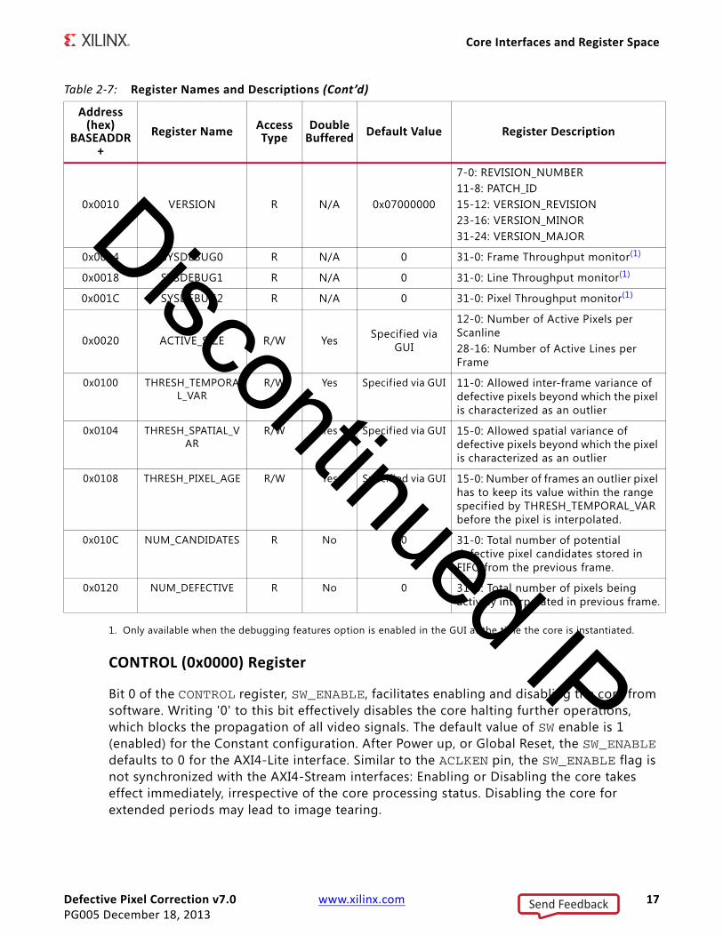
Register SpaceThe standardized Xilinx Video IP register space is partitioned to control-, timing-, and core specific registers. The DPC core uses only one timing related register, ACTIVE_SIZE (0x0020), which allows specifying the input frame dimensions. Also, the core has the following core-specific registers, THRESH_TEMPORAL_VAR (0x0100), THRESH_SPATIAL_VAR (0x0104), THRESH_PIXEL_AGE (0x0108) which allows specifying the characteristics of the defective pixels from the image sensor, as described in THRESH_TEMPORAL_VAR (0x0100), THRESH_SPATIAL_VAR (0x0104), THRESH_PIXEL_AGE (0x0108) registers.
Table 2-7: Register Names and Descriptions
Address (hex)
BASEADDR +
Register Name Access Type
Double Buffered Default Value Register Description
0x0000 CONTROL R/W N Power-on-Reset: 0x0
Bit 0: SW_ENABLEBit 1: REG_UPDATEBit 4: BYPASS(1)
Bit 5: TEST_PATTERN(1)
Bit 30: FRAME_SYNC_RESET (1: reset)Bit 31: SW_RESET (1: reset)
0x0004 STATUS R/W No 0Bit 0: PROC_STARTED Bit 1: EOF Bit 16: SLAVE_ERROR
0x0008 ERROR R/W No 0
Bit 0: SLAVE_EOL_EARLY Bit 1: SLAVE_EOL_LATE Bit 2: SLAVE_SOF_EARLY Bit 3: SLAVE_SOF_LATE
0x000C IRQ_ENABLE R/W No 0 16-0: Interrupt enable bits corresponding to STATUS bits
Send Feedback
Discontinued IP
Defective Pixel Correction v7.0 www.xilinx.com 17PG005 December 18, 2013
Core Interfaces and Register Space
1. Only available when the debugging features option is enabled in the GUI at the time the core is instantiated.
CONTROL (0x0000) Register
Bit 0 of the CONTROL register, SW_ENABLE, facilitates enabling and disabling the core from software. Writing '0' to this bit effectively disables the core halting further operations, which blocks the propagation of all video signals. The default value of SW enable is 1 (enabled) for the Constant configuration. After Power up, or Global Reset, the SW_ENABLE defaults to 0 for the AXI4-Lite interface. Similar to the ACLKEN pin, the SW_ENABLE flag is not synchronized with the AXI4-Stream interfaces: Enabling or Disabling the core takes effect immediately, irrespective of the core processing status. Disabling the core for extended periods may lead to image tearing.
0x0010 VERSION R N/A 0x07000000
7-0: REVISION_NUMBER 11-8: PATCH_ID 15-12: VERSION_REVISION 23-16: VERSION_MINOR 31-24: VERSION_MAJOR
0x0014 SYSDEBUG0 R N/A 0 31-0: Frame Throughput monitor(1)
0x0018 SYSDEBUG1 R N/A 0 31-0: Line Throughput monitor(1)
0x001C SYSDEBUG2 R N/A 0 31-0: Pixel Throughput monitor(1)
0x0020 ACTIVE_SIZE R/W Yes Specified via GUI
12-0: Number of Active Pixels per Scanline 28-16: Number of Active Lines per Frame
0x0100 THRESH_TEMPORAL_VAR
R/W Yes Specif ied via GUI 11-0: Allowed inter-frame variance of defective pixels beyond which the pixel is characterized as an outlier
0x0104 THRESH_SPATIAL_VAR
R/W Yes Specif ied via GUI 15-0: Allowed spatial variance of defective pixels beyond which the pixel is characterized as an outlier
0x0108 THRESH_PIXEL_AGE R/W Yes Specif ied via GUI 15-0: Number of frames an outlier pixel has to keep its value within the range specif ied by THRESH_TEMPORAL_VAR before the pixel is interpolated.
0x010C NUM_CANDIDATES R No 0 31-0: Total number of potential defective pixel candidates stored in FIFO from the previous frame.
0x0120 NUM_DEFECTIVE R No 0 31-0: Total number of pixels being actively interpolated in previous frame.
Table 2-7: Register Names and Descriptions (Cont’d)
Address (hex)
BASEADDR +
Register Name Access Type
Double Buffered Default Value Register Description
Send Feedback
Discontinued IP
Defective Pixel Correction v7.0 www.xilinx.com 18PG005 December 18, 2013
Core Interfaces and Register Space
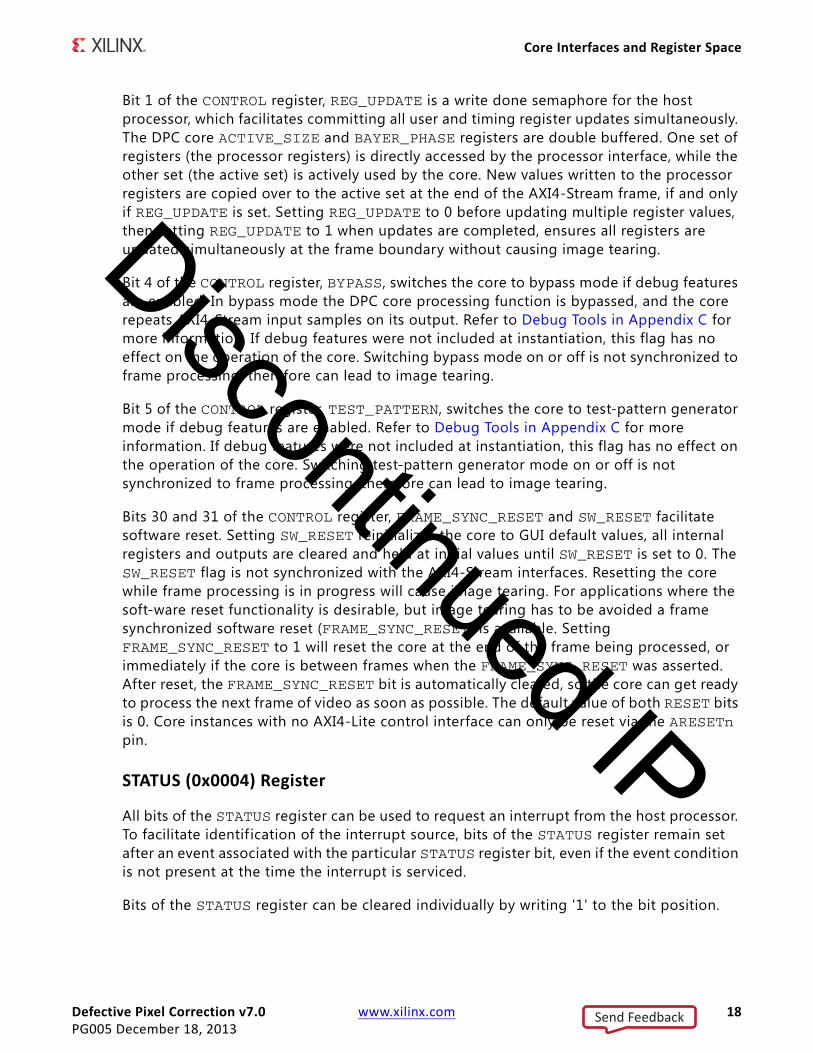
Bit 1 of the CONTROL register, REG_UPDATE is a write done semaphore for the host processor, which facilitates committing all user and timing register updates simultaneously. The DPC core ACTIVE_SIZE and BAYER_PHASE registers are double buffered. One set of registers (the processor registers) is directly accessed by the processor interface, while the other set (the active set) is actively used by the core. New values written to the processor registers are copied over to the active set at the end of the AXI4-Stream frame, if and only if REG_UPDATE is set. Setting REG_UPDATE to 0 before updating multiple register values, then setting REG_UPDATE to 1 when updates are completed, ensures all registers are updated simultaneously at the frame boundary without causing image tearing.
Bit 4 of the CONTROL register, BYPASS, switches the core to bypass mode if debug features are enabled. In bypass mode the DPC core processing function is bypassed, and the core repeats AXI4-Stream input samples on its output. Refer to Debug Tools in Appendix C for more information. If debug features were not included at instantiation, this flag has no effect on the operation of the core. Switching bypass mode on or off is not synchronized to frame processing, therefore can lead to image tearing.
Bit 5 of the CONTROL register, TEST_PATTERN, switches the core to test-pattern generator mode if debug features are enabled. Refer to Debug Tools in Appendix C for more information. If debug features were not included at instantiation, this flag has no effect on the operation of the core. Switching test-pattern generator mode on or off is not synchronized to frame processing, therefore can lead to image tearing.
Bits 30 and 31 of the CONTROL register, FRAME_SYNC_RESET and SW_RESET facilitate software reset. Setting SW_RESET reinitializes the core to GUI default values, all internal registers and outputs are cleared and held at initial values until SW_RESET is set to 0. The SW_RESET flag is not synchronized with the AXI4-Stream interfaces. Resetting the core while frame processing is in progress will cause image tearing. For applications where the soft-ware reset functionality is desirable, but image tearing has to be avoided a frame synchronized software reset (FRAME_SYNC_RESET) is available. Setting FRAME_SYNC_RESET to 1 will reset the core at the end of the frame being processed, or immediately if the core is between frames when the FRAME_SYNC_RESET was asserted. After reset, the FRAME_SYNC_RESET bit is automatically cleared, so the core can get ready to process the next frame of video as soon as possible. The default value of both RESET bits is 0. Core instances with no AXI4-Lite control interface can only be reset via the ARESETn pin.
STATUS (0x0004) Register
All bits of the STATUS register can be used to request an interrupt from the host processor. To facilitate identif ication of the interrupt source, bits of the STATUS register remain set after an event associated with the particular STATUS register bit, even if the event condition is not present at the time the interrupt is serviced.
Bits of the STATUS register can be cleared individually by writing '1' to the bit position.
Send Feedback
Discontinued IP

Defective Pixel Correction v7.0 www.xilinx.com 19PG005 December 18, 2013
Core Interfaces and Register Space
Bit 0 of the STATUS register, PROC_STARTED, indicates that processing of a frame has commenced via the AXI4-Stream interface.
Bit 1 of the STATUS register, End-of-frame (EOF), indicates that the processing of a frame has completed.
Bit 16 of the STATUS register, SLAVE_ERROR, indicates that one of the conditions monitored by the ERROR register has occurred.
ERROR (0x0008) Register
Bit 16 of the STATUS register, SLAVE_ERROR, indicates that one of the conditions monitored by the ERROR register has occurred. This bit can be used to request an interrupt from the host processor. To facilitate identif ication of the interrupt source, bits of the STATUS and ERROR registers remain set after an event associated with the particular ERROR register bit, even if the event condition is not present at the time the interrupt is serviced.
Bits of the ERROR register can be cleared individually by writing '1' to the bit position to be cleared.
Bit 0 of the ERROR register, EOL_EARLY, indicates an error during processing a video frame via the AXI4-Stream slave port. The number of pixels received between the latest and the preceding End-Of-Line (EOL) signal was less than the value programmed into the ACTIVE_SIZE register.
Bit 1 of the ERROR register, EOL_LATE, indicates an error during processing a video frame via the AXI4-Stream slave port. The number of pixels received between the last EOL signal surpassed the value programmed into the ACTIVE_SIZE register.
Bit 2 of the ERROR register, SOF_EARLY, indicates an error during processing a video frame via the AXI4-Stream slave port. The number of pixels received between the latest and the preceding Start-Of-Frame (SOF) signal was less than the value programmed into the ACTIVE_SIZE register.
Bit 3 of the ERROR register, SOF_LATE, indicates an error during processing a video frame via the AXI4-Stream slave port. The number of pixels received between the last SOF signal surpassed the value programmed into the ACTIVE_SIZE register.
IRQ_ENABLE (0x000C) Register
Any bits of the STATUS register can generate a host-processor interrupt request via the IRQ pin. The Interrupt Enable register facilitates selecting which bits of STATUS register will assert IRQ. Bits of the STATUS registers are masked by (AND) corresponding bits of the IRQ_ENABLE register and the resulting terms are combined (OR) together to generate IRQ.
Send Feedback
Discontinued IP
Defective Pixel Correction v7.0 www.xilinx.com 20PG005 December 18, 2013
Core Interfaces and Register Space
Version (0x0010) Register
Bit f ields of the Version Register facilitate software identif ication of the exact version of the hardware peripheral incorporated into a system. The core driver can take advantage of this Read-Only value to verify that the software is matched to the correct version of the hardware.
SYSDEBUG0 (0x0014) Register
The SYSDEBUG0, or Frame Throughput Monitor, register indicates the number of frames processed since power-up or the last time the core was reset. The SYSDEBUG registers can be useful to identify external memory / Frame buffer / or throughput bottlenecks in a video system. Refer to Debug Tools in Appendix C for more information.
SYSDEBUG1 (0x0018) Register
The SYSDEBUG1, or Line Throughput Monitor, register indicates the number of lines processed since power-up or the last time the core was reset. The SYSDEBUG registers can be useful to identify external memory / Frame buffer / or throughput bottlenecks in a video system. Refer to Debug Tools in Appendix C for more information.
SYSDEBUG2 (0x001C) Register
The SYSDEBUG2, or Pixel Throughput Monitor, register indicates the number of pixels processed since power-up or the last time the core was reset. The SYSDEBUG registers can be useful to identify external memory / Frame buffer / or throughput bottlenecks in a video system. Refer to Debug Tools in Appendix C for more information.
ACTIVE_SIZE (0x0020) Register
The ACTIVE_SIZE register encodes the number of active pixels per scan line and the number of active scan lines per frame. The lower half-word (bits 12:0) encodes the number of active pixels per scan line. Supported values are between 32 and the value provided in the Maximum number of pixels per scan line f ield in the GUI. The upper half-word (bits 28:16) encodes the number of active lines per frame. Supported values are 32 to 7680. To avoid processing errors, the user should restrict values written to ACTIVE_SIZE to the range supported by the core instance.
THRESH_TEMPORAL_VAR (0x0100) Register
Threshold value THRESH_TEMPORAL_VAR, defines the range a pixel value needs to stay in to be classif ied as stuck. The lower the value, the lower the chance that slowly varying pixels get characterized as stuck. However, if the sensor image is loaded with noise, or blooming may modify the readout values of dead pixels, THRESH_TEMPORAL_VAR may need to be increased to identify all stuck pixels. As a practical value for THRESH_TEMPORAL_VAR, the square root of the maximum pixel value is suggested.
Send Feedback
Discontinued IP

Defective Pixel Correction v7.0 www.xilinx.com 21PG005 December 18, 2013
Core Interfaces and Register Space
THRESH_SPATIAL_VAR (0x0104) Register
Threshold value THRESH_SPATIAL_VAR defines how different a pixel needs to be from the surrounding pixels to be classif ied as an outlier. A practical value of 2^DATA_WIDTH-5 identif ies pixels that visually stand out from their surroundings. A higher threshold value for THRESH_SPATIAL_VAR results in a lower number of outlier candidates and slower convergence time for identifying all outliers, but at the same time returns fewer false positives. If heuristics for the total number of outliers (M) are known, a feedback mechanism can be implemented that tunes THRESH_SPATIAL_VAR so that the number of outlier pixels identif ied, num_candidates, approximates M.
THRESH_PIXEL_AGE (0x0108) Register
Threshold value, THRESH_PIXEL_AGE, defines the number of frames presumed outliers have to hold their values within THRESH_TEMPORAL_VAR range before an outlier pixel is considered defective, and replacement (interpolation) of the pixels begin. The higher the value of THRESH_PIXEL_AGE, the less flickering due to incorrect defective pixel correction the algorithm produces, but also the longer it takes for the algorithm to converge and start replacing defective pixels. Values in the range of several thousands allow virtually no flickering while identifying outliers within minutes.
NUM_CANDIDATES (0x010C) Register
This read only register returns the number of potential defective pixel candidates stored in memory from the previous frame.
NUM_DEFECTIVE (0x0120) Register
This read only register returns the number of pixels actively being interpolated from the previous frame.
The Interrupt Subsystem
STATUS register bits can trigger interrupts so embedded application developers can quickly identify faulty interfaces or incorrectly parameterized cores in a video system. Irrespective of whether the AXI4-Lite control interface is present or not, the CCM core detects AXI4-Stream framing errors, as well as the beginning and the end of frame processing.
When the core is instantiated with an AXI4-Lite Control interface, the optional interrupt request pin (IRQ) is present. Events associated with bits of the STATUS register can generate a (level triggered) interrupt, if the corresponding bits of the interrupt enable register (IRQ_ENABLE) are set. After set by the corresponding event, bits of the STATUS register stay set until the user application clears them by writing '1' to the desired bit positions. Using this mechanism the system processor can identify and clear the interrupt source.
Send Feedback
Discontinued IP

Defective Pixel Correction v7.0 www.xilinx.com 22PG005 December 18, 2013
Core Interfaces and Register Space
Without the AXI4-Lite interface, the application can still benefit from the core signaling error and status events. By selecting Enable INTC Port, the core generates the optional INTC_IF port. This vector of signals gives parallel access to the individual interrupt sources, as seen in Table 2-8.
Unlike STATUS and ERROR flags, INTC_IF signals are not held, rather stay asserted only while the corresponding event persists.
In a system integration tool, the interrupt controller INTC IP can be used to register the selected INTC_IF signals as edge triggered interrupt sources. The INTC IP provides functionality to mask (enable or disable), as well as identify individual interrupt sources from software. Alternatively, for an external processor or MCU, you can custom build a priority interrupt controller to aggregate interrupt requests and identify interrupt sources.
Table 2-8: INTC_IF Signal Functions
INTC_IF signal Function
0 Frame processing start
1 Frame processing complete
2 Reserved
3 Reserved
4 Video over AXI4-Stream Error
5 EOL Early
6 EOL Late
7 SOF Early
8 SOF Late
Send Feedback
Discontinued IP

Defective Pixel Correction v7.0 www.xilinx.com 23PG005 December 18, 2013
Chapter 3
Designing with the Core
General Design GuidelinesThe DPC core corrects defective pixels from a Bayer sub-sampled image sensor data to downstream processing modules. The resulting video stream remains Bayer sub-sampled.
The core processes samples provided via an AXI4-Stream slave interface, outputs pixels via an AXI4-Stream master interface, and can be controlled via an optional AXI4-Lite interface.
RECOMMENDED: It is recommended that the DPC core is used in conjunction with the Video In to AXI4-Stream and Video Timing Controller cores.
The Video Timing Controller core measures the timing parameters, such as number of active scan lines, number of active pixels per scan line of the image sensor. The Video In to AXI4-Stream core formats the input video to the AXI4-Stream interface.
Typically, the Defective Pixel Correction core is part of an Image Sensor Pipeline (ISP) System, as shown in Figure 3-1.
Send Feedback
Discontinued IP

Defective Pixel Correction v7.0 www.xilinx.com 24PG005 December 18, 2013
Clock, Enable, and Reset Considerations
Clock, Enable, and Reset Considerations
ACLKThe master and slave AXI4-Stream video interfaces use the ACLK clock signal as their shared clock reference, as shown in Figure 3-2.
S_AXI_ACLKThe AXI4-Lite interface uses the A_AXI_ACLK pin as its clock source. The ACLK pin is not shared between the AXI4-Lite and AXI4-Stream interfaces. The Defective Pixel Correction
X-Ref Target - Figure 3-1
Figure 3-1: Image Sensor Pipeline System with Defective Pixel Correction Core
X-Ref Target - Figure 3-2
Figure 3-2: Example of ACLK Routing in an ISP Processing Pipeline
Send Feedback
Discontinued IP

Defective Pixel Correction v7.0 www.xilinx.com 25PG005 December 18, 2013
Clock, Enable, and Reset Considerations
core contains clock-domain crossing logic between the ACLK (AXI4-Stream and Video Processing) and S_AXI_ACLK (AXI4-Lite) clock domains. The core automatically ensures that the AXI4-Lite transactions completes even if the video processing is stalled with ARESETn, ACLKEN or with the video clock not running.
ACLKENThe Defective Pixel Correction core has two enable options: the ACLKEN pin (hardware clock enable), and the software reset option provided through the AXI4-Lite control interface (when present).
ACLKEN may not be synchronized internally to AXI4-Stream frame processing therefore de-asserting ACLKEN for extended periods of time may lead to image tearing.
The ACLKEN pin facilitates:
• Multi-cycle path designs (high speed clock division without clock gating)
• Standby operation of subsystems to save on power
• Hardware controlled bring-up of system components
IMPORTANT: When ACLKEN (clock enable) pins are used (toggled) in conjunction with a common clock source driving the master and slave sides of an AXI4-Stream interface, to prevent transaction errors the ACLKEN pins associated with the master and slave component interfaces must also be driven by the same signal (Figure 2-2).
IMPORTANT: When two cores connected through AXI4-Stream interfaces, where only the master or the slave interface has an ACLKEN port, which is not permanently tied high, the two interfaces should be connected through the AXI4-Stream Interconnect or AXI-FIFO cores to avoid data corruption (Figure 2-3).
S_AXI_ACLKENThe S_AXI_ACLKEN is the clock enable signal for the AXI4-Lite interface only. Driving this signal Low only affects the AXI4-Lite interface and does not halt the video processing in the ACLK clock domain.
ARESETnThe Defective Pixel Correction core has two reset source: the ARESETn pin (hardware reset), and the software reset option provided through the AXI4-Lite control interface (when present).
Send Feedback
Discontinued IP

Defective Pixel Correction v7.0 www.xilinx.com 26PG005 December 18, 2013
System Considerations
IMPORTANT: ARESETn is not synchronized internally to AXI4-Stream frame processing. Deasserting ARESETn while a frame is being process leads to image tearing.
The external reset pulse needs to be held for 32 ACLK cycles to reset the core. The ARESETn signal only resets the AXI4-Stream interfaces. The AXI4-Lite interface is unaffected by the ARESETn signal to allow the video processing core to be reset without halting the AXI4-Lite interface.
IMPORTANT: When a system with multiple-clocks and corresponding reset signals are being reset, the reset generator has to ensure all signals are asserted/de-asserted long enough so that all interfaces and clock-domains are correctly reinitialized.
S_AXI_ARESETnThe S_AXI_ARESETn signal is synchronous to the S_AXI_ACLK clock domain, but is internally synchronized to the ACLK clock domain. The S_AXI_ARESETn signal resets the entire core including the AXI4-Lite and AXI4-Stream interfaces.
System ConsiderationsThe DPC must be configured for the actual video frame-size to operate properly. To gather the frame size information from the video, it can be connected to the Video In to AXI4-Stream input and the Video Timing Controller. The timing detector logic in the Video Timing Controller will gather the video timing signals. The AXI4-Lite control interface on the Video Timing Controller allows the system processor to read out the measured frame dimensions, and program all downstream cores, such as the DPC, with the appropriate image dimensions.
If the target system uses only one setup of the DPC, the you may choose to create a constant configuration by removing the AXI4-Lite interface. This option reduces the core Slice footprint.
Clock Domain InteractionThe ARESETn and ACLKEN input signals will not reset or halt the AXI4-Lite interface. This allows the video processing to be reset or halted separately from the AXI4-Lite interface without disrupting AXI4-Lite transactions.
The AXI4-Lite interface will respond with an error if the core registers cannot be read or written within 128 S_AXI_ACLK clock cycles. The core registers cannot be read or written if the ARESETn signal is held low, if the ACLKEN signal is held low or if the ACLK signal is not connected or not running. If core register read does not complete, the AXI4-Lite read transaction will respond with 10 on the S_AXI_RRESP bus. Similarly, if a core register write
Send Feedback
Discontinued IP
Defective Pixel Correction v7.0 www.xilinx.com 27PG005 December 18, 2013
System Considerations
does not complete, the AXI4-Lite write transaction will respond with 10 on the S_AXI_BRESP bus. The S_AXI_ARESETn input signal resets the entire core.
Programming SequenceIf processing parameters such as the image size needs to be changed on-the-fly, or the system needs to be reinitialized, it is recommended that pipelined Xilinx IP video cores be disabled/reset from system output towards the system input, and programmed/enabled from system input to system output. STATUS register bits allow system processors to identify the processing states of individual constituent cores, and successively disable a pipeline as one core after another is f inished processing the last frame of data.
Error Propagation and RecoveryParameterization and/or configuration registers define the dimensions of video frames that video IP should process. Starting from a known state, and based on these configuration settings the IP can predict when the beginning of the next frame is expected. Similarly, the IP can predict when the last pixel of each scan line is expected. SOF detected before it was expected (early), or SOF not present when it is expected (late), EOL detected before expected (early), or EOL not present when expected (late), signals error conditions indicative of either upstream communication errors or incorrect core configuration.
When SOF is detected early, the output SOF signal is generated early, terminating the previous frame immediately. When SOF is detected late, the output SOF signal is generated according to the programmed values. Extra lines / pixels from the previous frame are dropped until the input SOF is captured.
Similarly, when EOL is detected early, the output EOL signal is generated early, terminating the previous line immediately. When EOL is detected late, the output EOL signal is generated according to the programmed values. Extra pixels from the previous line are dropped until the input EOL is captured.
Send Feedback
Discontinued IP

Defective Pixel Correction v7.0 www.xilinx.com 28PG005 December 18, 2013
Chapter 4
Customizing and Generating the CoreThis chapter includes information about using Xilinx tools to customize and generate the core in the Vivado Design Suite environment.
Vivado Integrated Design Environment (IDE)You can customize the IP for use in your design by specifying values for the various parameters associated with the IP core using the following steps:
1. Select the IP from the IP catalog.
2. Double-click on the selected IP or select the Customize IP command from the toolbar or popup menu.
For details, see the sections, “Working with IP” and “Customizing IP for the Design” in the Vivado Design Suite User Guide: Designing with IP (UG896) [Ref 3] and the “Working with the Vivado IDE” section in the Vivado Design Suite User Guide: Getting Started (UG910) [Ref 5].
If you are customizing and generating the core in the Vivado IP Integrator, see the Vivado Design Suite User Guide: Designing IP Subsystems Using IP Integrator (UG994) [Ref 7] for detailed information. IP Integrator might auto-compute certain configuration values when validating or generating the design. To check whether the values do change, see the description of the parameter in this chapter. To view the parameter value you can run the validate_bd_design command in the Tcl console.
Note: Figures in this chapter are illustrations of the Vivado IDE. This layout might vary from the current version.
Interface The Defective Pixel Correction core is easily configured to meet the developer's specif ic needs through the Vivado tools interface. This section provides a quick reference to parameters that can be configured at generation time.
Send Feedback
Discontinued IP

Defective Pixel Correction v7.0 www.xilinx.com 29PG005 December 18, 2013
Interface
The GUI (Figure 4-1) displays a representation of the IP symbol on the left side, and the parameter assignments on the right side, which are described as follows:
• Component Name: The component name is used as the base name of output f iles generated for the module. Names must begin with a letter and must be composed from characters: a to z, 0 to 9 and “_”. The name v_spc_v7_0 cannot be used as a component name.
• Video Component Width: Specif ies the bit width of the input channel. Permitted values are 8, 10, and 12 bits. When using IP Integrator, this parameter is automatically computed based on the Video Component Width of the video IP core connected to the slave AXI-Stream video interface.
• Optional Features:
° AXI4-Lite Register Interface: When selected, the core will be generated with an AXI4-Lite interface, which gives access to dynamically program and change processing parameters. For more information, refer to Control Interface in Chapter 2.
° Include Debug Features: When selected, the core will be generated with debugging features, which simplify system design, testing and debugging. For more information, refer to Debugging Features in Appendix C.
IMPORTANT: Debugging features are only available when the AXI4-Lite Register Interface is selected.
X-Ref Target - Figure 4-1
Figure 4-1: DPC IP Catalog
Send Feedback
Discontinued IP
Defective Pixel Correction v7.0 www.xilinx.com 30PG005 December 18, 2013
Interface
° Enable INTC Port: When selected, the core will generate the optional INTC_IF port, which gives parallel access to signals indicating frame processing status and error conditions. For more information, refer to The Interrupt Subsystem in Chapter 2.
• Defective Pixels Tracked: This option specif ies the maximum number of potential defective pixels. Candidate defective pixels will be stored in Block RAMs.
• Temporal Variance Threshold: This option defines the range a pixel value needs to stay in to be classif ied as stuck. The lower the value, the lower the chance that slowly varying pixels get characterized as stuck. However, if the sensor image is loaded with noise, or blooming may modify the readout values of dead pixels, this option may need to be increased to identify all stuck pixels. As a practical value, the square root of the maximum pixel value is suggested.
• Spatial Variance Threshold: Spatial Variance Threshold defines how different a pixel needs to be from the surrounding pixels to be classif ied as an outlier. A practical value of 2^DATA_WIDTH-5 identif ies pixels that visually stand out from their surroundings. A higher threshold value results in a lower number of outlier candidates and slower convergence time for identifying all outliers, but at the same time returns fewer false positives. If heuristics for the total number of outliers (M) are known, a feedback mechanism can be implemented that tunes the threshold so that the number of outlier pixels identif ied, NUM_CANDIDATES, approximates M.
• Pixel Age: This option defines the number of frames presumed outliers have to hold their values within Temporal Threshold Variance range before an outlier pixel is considered defective, and replacement (interpolation) of the pixels begin. The higher the Pixel Age value, the less flickering due to incorrect defective pixel correction the algorithm produces, but also the longer it takes for the algorithm to converge and start replacing defective pixels. Values in the range of several thousands allow virtually no flickering while identifying outliers within minutes.
• Input Frame Dimensions:
° Number of Active Pixels per Scan line: When the AXI4-Lite control interface is enabled, the generated core will use the value specified in the CORE Generator GUI as the default value for the lower half-word of the ACTIVE_SIZE register. When an AXI4-Lite interface is not present, the GUI selection permanently defines the horizontal size of the frames the generated core instance is to process.
° Number of Active Lines per Frame: When the AXI4-Lite control interface is enabled, the generated core will use the value specified in the CORE Generator GUI as the default value for the upper half-word of the ACTIVE_SIZE register. When an AXI4-Lite interface is not present, the GUI selection permanently defines the vertical size (number of lines) of the frames the generated core instance is to process.
° Maximum Number of Active Pixels Per Scan line: Specif ies the maximum number of pixels per scan line that can be processed by the generated core instance. Permitted values are from 32 to 7680. Specifying this value is necessary to establish the depth of line buffers. The actual value selected for Number of Active Pixels per
Send Feedback
Discontinued IP

Defective Pixel Correction v7.0 www.xilinx.com 31PG005 December 18, 2013
Interface
Scan line, or the corresponding lower half-word of the ACTIVE_SIZE register must always be less than the value provided by Maximum Number of Active Pixels Per Scan line. Using a tight upper-bound results in optimal block RAM usage. This f ield is enabled only when the AXI4-Lite interface is selected. Otherwise contents of the f ield are reflecting the actual contents of the Number of Active Pixels per Scan line f ield as for constant mode the maximum number of pixels equals the active number of pixels.
Output GenerationFor details, see “Generating IP Output Products” in the Vivado Design Suite User Guide: Designing with IP (UG896).
Send Feedback
Discontinued IP
Defective Pixel Correction v7.0 www.xilinx.com 32PG005 December 18, 2013
Chapter 5
Constraining the Core
Required ConstraintsThe only constraints required are clock frequency constraints for the video clock, clk , and the AXI4-Lite clock, s_axi_aclk . Paths between the two clock domains should be constrained with a max_delay constraint and use the datapathonly flag, causing setup and hold checks to be ignored for signals that cross clock domains. These constraints are provided in the XDC constraints f ile included with the core.
Send Feedback
Discontinued IP
Defective Pixel Correction v7.0 www.xilinx.com 33PG005 December 18, 2013
Chapter 6
SimulationThis chapter contains information about simulating IP in the Vivado® Design Suite environment. For comprehensive information about Vivado simulation components, as well as information about using supported third party tools, see the Vivado Design Suite User Guide: Logic Simulation (UG900) [Ref 6].
Send Feedback
Discontinued IP

Defective Pixel Correction v7.0 www.xilinx.com 34PG005 December 18, 2013
Chapter 7
Synthesis and ImplementationFor details about synthesis and implementation, see “Synthesizing IP” and “Implementing IP” in the Vivado Design Suite User Guide: Designing with IP (UG896) [Ref 3].
Send Feedback
Discontinued IP
Defective Pixel Correction v7.0 www.xilinx.com 35PG005 December 18, 2013
Chapter 8
C Model Reference
Installation and Directory StructureThis chapter contains information for installing the Defective Pixel Correction C-Model, and describes the f ile contents and directory structure.
Software RequirementsThe Defective Pixel Correction v7.0 C-models were compiled and tested with the following software versions.
InstallationThe installation of the C-Model requires updates to the PATH variable, as described below.
Linux
Ensure that the directory in which the libIp_v_spc_v7_0_bitacc_cmodel.so f ile is located is in your $LD_LIBRARY_PATH environment variable.
Table 8-1: Supported Systems and Software Requirements
Platform C-Compiler
Linux 32-bit and 64-bit GCC 4.1.1
Windows 32-bit and 64-bit Visual Studio 2008 (Visual C++ 8.0)
Send Feedback
Discontinued IP

Defective Pixel Correction v7.0 www.xilinx.com 36PG005 December 18, 2013
Installation and Directory Structure
C-Model File ContentsUnzipping the v_spc_v7_0_bitacc_model.zip f ile creates the following directory structures and f iles which are described inTable 8-2.
Table 8-2: C-Model Files
File Description
/lin Pre-compiled bit accurate ANSI C reference model for simulation on 32-bit Linux Platforms
libIp_v_spc_v7_0_bitacc_cmodel.lib Defective Pixel Correction v7.0 model shared object library (Linux platforms only)
run_bitacc_cmodel Pre-compiled bit accurate executable for simulation on 32-bit Linux Platforms
/lin64 Pre-compiled bit accurate ANSI C reference model for simulation on 64-bit Linux Platforms
libIp_v_spc_v7_0_bitacc_cmodel.lib Defective Pixel Correction v7.0 model shared object library (Linux platforms only)
run_bitacc_cmodel Pre-compiled bit accurate executable for simulation on 32-bit Linux Platforms
/nt Pre-compiled bit accurate ANSI C reference model for simulation on 32-bit Windows Platforms
libIp_v_spc_v7_0_bitacc_cmodel.lib Pre-compiled library file for win32 compilation
run_bitacc_cmodel.exe Pre-compiled bit accurate executable for simulation on 32-bit Windows Platforms
/nt64 Pre-compiled bit accurate ANSI C reference model for simulation on 64-bit Windows Platforms
libIp_v_spc_v7_0_bitacc_cmodel.lib Pre-compiled library file for win32 compilation
run_bitacc_cmodel.exe Pre-compiled bit accurate executable for simulation on 64-bit Windows Platforms
README.txt Release notes
pg002_v_spc.pdf Defective Pixel Correction Interpolation Core Product Guide
v_spc_v7_0_bitacc_cmodel.h Model header file
rgb_utils.h Header f ile declaring the RGB image / video container type and support functions
bmp_utils.h Header file declaring the bitmap (.bmp) image file I/O functions
video_utils.h Header f ile declaring the generalized image / video container type, I/O and support functions.
Kodim19_128x192.bmp 128x192 sample test image of the Lighthouse image from the True-colorKodak test images
run_bittacc_cmodel.c Example code calling the C-Model
Send Feedback
Discontinued IP
Defective Pixel Correction v7.0 www.xilinx.com 37PG005 December 18, 2013
Using the C-Model
Using the C-ModelThe bit accurate C model is accessed through a set of functions and data structures that are declared in the v_spc_v7_0_bitacc_cmodel.h f ile.
Before using the model, the structures holding the inputs, generics and output of the DPC instance must be defined:
struct xilinx_ip_v_spc_v7_0_generics spc_generics;struct xilinx_ip_v_spc_v7_0_inputs spc_inputs;struct xilinx_ip_v_spc_v7_0_outputs spc_outputs;
The declaration of these structures is in the v_spc_v7_0_bitacc_cmodel.h f ile.
Table 8-3 lists the generic parameters taken by the DPC v7.0 IP core bit accurate model, as well as the default values. For an actual instance of the core, these parameters can only be set in generation time through the GUI.
Calling xilinx_ip_v_spc_v7_0_get_default_generics(&spc_generics) initializes the generics structure with the DPC GUI defaults, listed in Table 8-3.
The structure spc_inputs defines the values of run time parameters and the actual input image. Calling xilinx_ip_v_spc_v7_0_get_default_inputs(&spc_generics, &spc_inputs) initializes the input structure with the DPC GUI default values (see Table 8-3).
Table 8-3: Model Generic Parameters and Default Values
Generic Variable Type Default Value Range Description
DATA_WIDTH int 8 8,10,12 Input / output data width
STATUS_WIDTH int 10 9 - 13 2^STATUS_WIDTH number of defective pixels tracked
MAX_COLS int 1920 32 - 7680 Maximum number of columns that the input video will have. Must be greater than ACTIVE_COLS
ACTIVE_COLS int 1920 32 - 7680 Maximum number of columns in the active video
ACTIVE_ROWS int 1080 32 - 7680 Maximum number of rows in the active video
THRESH_PIXEL_AGE int 1200 0 - 65535 The number of frames a potential defective pixel will be tracked
THRESH_SPATIAL_VAR int 6554 0 - 65535 The variance of the potential defective pixel against the neighboring pixels. Outside of the variance, the pixel will be considered defective.
THRESH_TEMPORAL_VAR int 2 0 - 65535 The variance of the potential defective pixel between frames. Outside of the variance, the pixel will be considered defective.
Send Feedback
Discontinued IP
Defective Pixel Correction v7.0 www.xilinx.com 38PG005 December 18, 2013
Using the C-Model
Note: The video_in variable is not initialized because the initialization depends on the actual test image to be simulated. Initializing the DPC Input Video Structure describes the initialization of the video_in structure.
After the inputs are defined, the model can be simulated by calling this function:
int xilinx_ip_v_spc_v7_0_bitacc_simulate(struct xilinx_ip_v_spc_v7_0_generics* generics,struct xilinx_ip_v_spc_v7_0_inputs* inputs,struct xilinx_ip_v_spc_v7_0_outputs* outputs).
Results are included in the outputs structure, which contains only one member, type video_struct. After the outputs are evaluated and saved, dynamically allocated memory for input and output video structures must be released by calling this function:
void xilinx_ip_v_spc_v7_0_destroy(struct xilinx_ip_v_spc_v7_0_inputs *input, struct xilinx_ip_v_spc_v7_0_outputs *output).
Successful execution of all provided functions, except for the destroy function, return value 0. A non-zero error code indicates that problems occurred during function calls.
DPC Input and Output Video StructureInput images or video streams can be provided to the DPC v7.0 reference model using the video_struct structure, defined in video_utils.h:
struct video_struct{ int frames, rows, cols, bits_per_component, mode; uint16*** data[5]; };
Table 8-4: Member Variables of the Video Structure
Member Variable Designation
frames Number of video/image frames in the data structure.
rows Number of rows per frame.Pertaining to the image plane with the most rows and columns, such as the luminance channel for YUV data. Frame dimensions are assumed constant through all frames of the video stream. However different planes, such as y, u and v can have different dimensions.
cols Number of columns per frame.Pertaining to the image plane with the most rows and columns, such as the luminance channel for YUV data. Frame dimensions are assumed constant through all frames of the video stream. However different planes, such as y, u and v can have different dimensions.
bits_per_component Number of bits per color channel/component.All image planes are assumed to have the same color/component representation. Maximum number of bits per component is 16.
Send Feedback
Discontinued IP

Defective Pixel Correction v7.0 www.xilinx.com 39PG005 December 18, 2013
Using the C-Model
Initializing the DPC Input Video StructureThe easiest way to assign stimuli values to the input video structure is to initialize it with an image or video. The bmp_util.h and video_util.h header f iles packaged with the bit accurate C models contain functions to facilitate file I/O.
Bitmap Image Files
The header bmp_utils.h declares functions that help access f iles in Windows Bitmap format (http://en.wikipedia.org/wiki/BMP_file_format). However, this format limits color depth to a maximum of 8-bits per pixel, and operates on images with three planes (R,G,B). Consequently, the following functions operate on arguments type rgb8_video_struct, which is defined in rgb_utils.h. Also, both functions support only true-color, non-indexed formats with 24-bits per pixel.
mode Contains information about the designation of data planes.Named constants to be assigned to mode are listed in Table 8-5.
data Set of f ive pointers to three dimensional arrays containing data for image planes.Data is in 16-bit unsigned integer format accessed as data[plane][frame][row][col].
Table 8-5: Named Video Modes with Corresponding Planes and Representations
Mode(1) Planes Video Representation
FORMAT_MONO 1 Monochrome – Luminance only
FORMAT_RGB 3 RGB image/video data
FORMAT_C444 3 444 YUV, or YCrCb image/video data
FORMAT_C422 3 422 format YUV video, (u, v chrominance channels horizontally sub-sampled)
FORMAT_C420 3 420 format YUV video, ( u, v sub-sampled both horizontally and vertically )
FORMAT_MONO_M 3 Monochrome (Luminance) video with Motion
FORMAT_RGBA 4 RGB image/video data with alpha (transparency) channel
FORMAT_C420_M 5 420 YUV video with Motion
FORMAT_C422_M 5 422 YUV video with Motion
FORMAT_C444_M 5 444 YUV video with Motion
FORMAT_RGBM 5 RGB video with Motion
1. The Defective Pixel Correction core supports Modes FORMAT_RGB and FORMAT_C444.
Table 8-4: Member Variables of the Video Structure (Cont’d)
Send Feedback
Discontinued IP

Defective Pixel Correction v7.0 www.xilinx.com 40PG005 December 18, 2013
Using the C-Model
int write_bmp(FILE *outfile, struct rgb8_video_struct *rgb8_video);int read_bmp(FILE *infile, struct rgb8_video_struct *rgb8_video);
Exchanging data between rgb8_video_struct and general video_struct type frames/videos is facilitated by these functions:
int copy_rgb8_to_video(struct rgb8_video_struct* rgb8_in, struct video_struct* video_out );
int copy_video_to_rgb8(struct video_struct* video_in, struct rgb8_video_struct* rgb8_out );
Note: All image/video manipulation utility functions expect both input and output structures initialized; for example, pointing to a structure that has been allocated in memory, either as static or dynamic variables. Moreover, the input structure must have the dynamically allocated container (data or r, g, b) structures already allocated and initialized with the input frame(s). If the output container structure is pre-allocated at the time of the function call, the utility functions verify and issue an error if the output container size does not match the size of the expected output. If the output container structure is not pre-allocated, the utility functions create the appropriate container to hold results.
Binary Image/Video Files
The video_utils.h header f ile declares functions that help load and save generalized video f iles in raw, uncompressed format.
int read_video( FILE* infile, struct video_struct* in_video);int write_video(FILE* outfile, struct video_struct* out_video);
These functions serialize the video_struct structure. The corresponding file contains a small, plain text header defining, "Mode", "Frames", "Rows", "Columns", and "Bits per Pixel". The plain text header is followed by binary data, 16-bits per component in scan line continuous format. Subsequent frames contain as many component planes as defined by the video mode value selected. Also, the size (rows, columns) of component planes can differ within each frame as defined by the actual video mode selected.
Working with Video_struct Containers
The video_utils.h header f ile defines functions to simplify access to video data in video_struct.
int video_planes_per_mode(int mode);int video_rows_per_plane(struct video_struct* video, int plane);int video_cols_per_plane(struct video_struct* video, int plane);
The video_planes_per_mode function returns the number of component planes defined by the mode variable, as described in Table 8-5. The video_rows_per_plane and video_cols_per_plane functions return the number of rows and columns in a given plane of the selected video structure. The following example demonstrates using these functions in conjunction to process all pixels within a video stream stored in the in_video variable:
for (int frame = 0; frame < in_video->frames; frame++) {
Send Feedback
Discontinued IP

Defective Pixel Correction v7.0 www.xilinx.com 41PG005 December 18, 2013
Using the C-Model
for (int plane = 0; plane < video_planes_per_mode(in_video->mode); plane++) { for (int row = 0; row < rows_per_plane(in_video,plane); row++) { for (int col = 0; col < cols_per_plane(in_video,plane); col++) {
// User defined pixel operations on // in_video->data[plane][frame][row][col] } } }}
C Model Example CodeAn example C f ile, run_bitacc_cmodel.c, is provided to demonstrate the steps required to run the model. After following the compilation instructions, run the example executable. The executable takes the path/name of the input f ile and the path/name of the output f ile as parameters. If invoked with insufficient parameters, this help message is issued:
Usage: run_bitacc_cmodel in_file out_file
in_file : path/name of the input BMP file
out_file : path/name of the output BMP file
During successful execution, two f iles with a .bin extension are created. The first f ile corresponds to the input BMP image, with the same path and name as the input f ile, and a .bin extension. The other f ile similarly corresponds to the output f ile. These files contain the inputs and outputs of the DPC algorithm in full precision, as the BMP format does not support color resolutions beyond 8-bits per component. The structure of .bin files are described in Binary Image/Video Files.
Send Feedback
Discontinued IP

Defective Pixel Correction v7.0 www.xilinx.com 42PG005 December 18, 2013
Compiling with the DPC C-Model
Compiling with the DPC C-Model
Linux (32- and 64-bit)To compile the example code, f irst ensure that the directory in which the file libIp_v_spc_v7_0_bitacc_cmodel.so is located is present in your $LD_LIBRARY_PATH environment variable. These shared libraries are referenced during the compilation and linking process. Then cd into the directory where the header f iles, library f iles and run_bitacc_cmodel.c were unpacked. The libraries and header f iles are referenced during the compilation and linking process.
Place the header f ile and C source f ile in a single directory. Then in that directory, compile using the GNU C Compiler:
gcc -m32 -x c++ ../run_bitacc_cmodel.c ../parsers.c -o run_bitacc_cmodel -L. -lIp_v_spc_v7_0_bitacc_cmodel -Wl,-rpath,.
gcc -m64 -x c++ ../run_bitacc_cmodel.c ../parsers.c -o run_bitacc_cmodel -L. -lIp_v_spc_v7_0_bitacc_cmodel -Wl,-rpath,.
Windows (32- and 64-bit)Precompiled library v_spc_v7_0_bitacc_cmodel.dll, and top level demonstration code run_bitacc_cmodel.c should be compiled with an ANSI C compliant compiler under Windows. Here an example is presented using Microsoft Visual Studio.
In Visual Studio create a new, empty Windows Console Application project. As existing items, add:
• The llibIpv_spc_v7_0_bitacc_cmodel.dll f ile to the "Resource Files" folder of the project
• The run_bitacc_cmodel.c f ile to the "Source Files" folder of the project
• The v_spc_v7_0_bitacc_cmodel.h header f iles to "Header Files" folder of the project (optional)
After the project has been created and populated, it needs to be compiled and linked (built) to create a win32 executable. To perform the build step, choose Build Solution from the Build menu. An executable matching the project name has been created either in the Debug or Release subdirectories under the project location based on whether Debug or Release has been selected in the Configuration Manager under the Build menu.
Send Feedback
Discontinued IP
Defective Pixel Correction v7.0 www.xilinx.com 43PG005 December 18, 2013
Chapter 9
Detailed Example DesignNo example design is available at the time for the LogiCORE IP Defective Pixel Correction v7.0 core.
Send Feedback
Discontinued IP

Defective Pixel Correction v7.0 www.xilinx.com 44PG005 December 18, 2013
Chapter 10
Test BenchThis chapter contains information about the provided test bench in the Vivado® Design Suite environment.
Demonstration Test BenchA demonstration test bench is provided with the core which enables you to observe core behavior in a typical scenario. This test bench is generated together with the core in Vivado Design Suite. You are encouraged to make simple modif ications to the configurations and observe the changes in the waveform.
Directory and File ContentsThe following files are expected to be generated in the in the demonstration test bench output directory:
• axi4lite_mst.v
• axi4s_video_mst.v
• axi4s_video_slv.v
• ce_generator.v
• tb_<IP_instance_name>.v
Test Bench StructureThe top-level entity is tb_<IP_instance_name>.
It instantiates the following modules:
• DUT
The <IP> core instance under test.
• axi4lite_mst
Send Feedback
Discontinued IP

Defective Pixel Correction v7.0 www.xilinx.com 45PG005 December 18, 2013
Chapter 10: Test Bench
The AXI4-Lite master module, which initiates AXI4-Lite transactions to program core registers.
• axi4s_video_mst
The AXI4-Stream master module, which generates ramp data and initiates AXI4-Stream transactions to provide video stimuli for the core and can also be used to open stimuli f iles generated from the reference C models and convert them into corresponding AXI4-Stream transactions.
To do this, edit tb_<IP_instance_name>.v:
a. Add define macro for the stimuli f ile name and directory pathdefine STIMULI_FILE_NAME<path><filename>.
b. Comment-out/remove the following line:MST.is_ramp_gen(`C_ACTIVE_ROWS, `C_ACTIVE_COLS, 2);and replace with the following line:MST.use_file(`STIMULI_FILE_NAME);
For information on how to generate stimuli f iles, see Chapter 4, C Model Reference.
• axi4s_video_slv
The AXI4-Stream slave module, which acts as a passive slave to provide handshake signals for the AXI4-Stream transactions from the core output, can be used to open the data files generated from the reference C model and verify the output from the core.
To do this, edit tb_<IP_instance_name>.v:
a. Add define macro for the golden f ile name and directory pathdefine GOLDEN_FILE_NAME “<path><filename>”.
b. Comment out the following line:SLV.is_passive;and replace with the following line:SLV.use_file(`GOLDEN_FILE_NAME);
For information on how to generate golden f iles, see Chapter 4, C Model Reference.
• ce_gen
Programmable Clock Enable (ACLKEN) generator.
Send Feedback
Discontinued IP

Defective Pixel Correction v7.0 www.xilinx.com 46PG005 December 18, 2013
Appendix A
Verification, Compliance, and Interoperability
SimulationA highly parameterizable test bench was used to test the Defective Pixel Correction core. Testing included the following:
• Register accesses
• Processing multiple frames of data
• AXI4-Stream bidirectional data-throttling tests
• Testing detection, and recovery from various AXI4-Stream framing error scenarios
• Testing different ACLKEN and ARESETn assertion scenarios
• Testing of various frame sizes
• Varying parameter settings
Hardware TestingThe Defective Pixel Correction core has been validated in hardware at Xilinx to represent a variety of parameterizations, including the following:
• A test design was developed for the core that incorporated a MicroBlaze™ processor, AXI4-Lite interconnect and various other peripherals. The software for the test system included pre-generated input and output data along with live video stream. The MicroBlaze processor was responsible for:
° Initializing the appropriate input and output buffers
° Initializing the Color Filer Array Interpolation core
° Launching the test
° Comparing the output of the core against the expected results
Send Feedback
Discontinued IP
Defective Pixel Correction v7.0 www.xilinx.com 47PG005 December 18, 2013
Interoperability
° Reporting the Pass/Fail status of the test and any errors that were found
InteroperabilityThe core slave (input) AXI4-Stream interface can work directly with the Video Input core. The core master (output) interface can work directly with the Color Filter Array Interpolation Xilinx Video core.
Send Feedback
Discontinued IP

Defective Pixel Correction v7.0 www.xilinx.com 48PG005 December 18, 2013
Appendix B
Migrating and UpgradingThis appendix contains information about migrating from an ISE design to the Vivado Design Suite, and for upgrading to a more recent version of the IP core. For customers upgrading their IP core, important details (where applicable) about any port changes and other impact to user logic are included.
Migrating to the Vivado Design SuiteFor information about migration to Vivado Design Suite, see ISE to Vivado Design Suite Migration Guide (UG911) [Ref 2].
Upgrading in Vivado Design SuiteThis section provides information about any changes to the user logic or port designations that take place when you upgrade to a more current version of this IP core in the Vivado Design Suite.
Parameter ChangesThere are no parameter changes.
Port ChangesThere are no port changes.
Other ChangesFrom version v4.0 to v5.00.a of the DPC core the following signif icant changes took place:
• XSVI interfaces were replaced by AXI4-Stream interfaces
• Since AXI4-Stream does not carry video timing data, the timing detector and timing generator modules were trimmed.
Send Feedback
Discontinued IP

Defective Pixel Correction v7.0 www.xilinx.com 49PG005 December 18, 2013
Upgrading in Vivado Design Suite
• The pCore, General Purpose Processor and Transparent modes became obsolete and were removed
• Native support for EDK have been added - the DPC core appears in the EDK IP Catalog
• Debugging features have been added
• The AXI4-Lite control interface register map is standardized between Xilinx video cores
From v5.00.a to v6.01.a of the DPC core, the following changes took place:
• The core originally had aclk , aclken and aresetn to control both the Video over AXI4-Stream and AXI4-Lite interfaces. Separate clock, clock enable and reset pins now control the Video over AXI4-Stream and the AXI4-Lite interfaces with clock domain crossing logic added to the core to handle the dissimilar clock domains between the AXI4-Lite and Video over AXI4-Stream domains.
Because of the complex nature of these changes, replacing a v4.0 version of the core in a customer design is not trivial. An existing EDK pCore, Transparent, or Constant DPC instance can be converted from XSVI to AXI4-Stream, the Video in to AXI4-Stream core or using components from XAPP521 (v1.0), Bridging Xilinx Streaming Video Interface with the AXI4-Stream Protocol located at:http://www.xilinx.com/support/documentation/application_notes/xapp521_XSVI_AXI4.pdf.
A v4.0 pCore instance in EDK can be replaced from v6.01.a directly from the EDK IP Catalog. However, the application software needs to be updated for the changed functionality and addresses of the DPC's registers. Consider replacing a legacy DPC pCore from EDK with a v6.01.a instance without AXI4-Lite interface to save resources.
If the user design explicitly used the timing detector or generator functionality of the DPC core, consider adding the Video Timing Controller core to migrate the functionality.
An ISE design using the General Purpose Processor interface, all of the above steps might be necessary:
• Timing detection, generation using the Video Timing Controller Core
• Replacing XSVI interfaces with conversion modules described in XAPP521 or try using the Video in to AXI4-Stream core
• Updating the DPC core instance to v6.01.a with or without AXI4-Lite interface
The INTC interface and debug functionality are new features for v6.01.a. When migrating an existing design, these functions may be disabled.
Send Feedback
Discontinued IP

Defective Pixel Correction v7.0 www.xilinx.com 50PG005 December 18, 2013
Appendix C
DebuggingThis appendix includes details about resources available on the Xilinx Support website and debugging tools.
Finding Help on Xilinx.comTo help in the design and debug process when using the Defective Pixel Correction, the Xilinx Support web page (www.xilinx.com/support) contains key resources such as product documentation, release notes, answer records, information about known issues, and links for opening a Technical Support WebCase.
DocumentationThis product guide is the main document associated with the Defective Pixel Correction. This guide, along with documentation related to all products that aid in the design process, can be found on the Xilinx Support web page (www.xilinx.com/support) or by using the Xilinx Documentation Navigator.
Download the Xilinx Documentation Navigator from the Design Tools tab on the Downloads page (www.xilinx.com/download). For more information about this tool and the features available, open the online help after installation.
Solution CentersSee the Xilinx Solution Centers for support on devices, software tools, and intellectual property at all stages of the design cycle. Topics include design assistance, advisories, and troubleshooting tips.
The Solution Center specif ic to the Defective Pixel Correction core is listed below.
• Xilinx Ethernet IP Solution Center
• Xilinx MIG Solution Center
• Xilinx Solution Center for PCI Express
Send Feedback
Discontinued IP

Defective Pixel Correction v7.0 www.xilinx.com 51PG005 December 18, 2013
Appendix C: Debugging
Answer RecordsAnswer Records include information about commonly encountered problems, helpful information on how to resolve these problems, and any known issues with a Xilinx product. Answer Records are created and maintained daily ensuring that users have access to the most accurate information available.
Answer Records for this core can also be located by using the Search Support box on the main Xilinx support web page. To maximize your search results, use proper keywords such as
• Product name
• Tool message(s)
• Summary of the issue encountered
A f ilter search is available after results are returned to further target the results.
Answer Records for the Defective Pixel Correction Core
AR 54521
Contacting Technical SupportXilinx provides technical support at www.xilinx.com/support for this LogiCORE™ IP product when used as described in the product documentation. Xilinx cannot guarantee timing, functionality, or support of product if implemented in devices that are not defined in the documentation, if customized beyond that allowed in the product documentation, or if changes are made to any section of the design labeled DO NOT MODIFY.
To contact Xilinx Technical Support:
1. Navigate to www.xilinx.com/support.
2. Open a WebCase by selecting the WebCase link located under Additional Resources.
When opening a WebCase, include:
• Target FPGA including package and speed grade.
• All applicable Xilinx Design Tools and simulator software versions.
• Additional f iles based on the specif ic issue might also be required. See the relevant sections in this debug guide for guidelines about which f ile(s) to include with the WebCase.
Note: Access to WebCase is not available in all cases. Please login to the WebCase tool to see your specif ic support options.
Send Feedback
Discontinued IP
Defective Pixel Correction v7.0 www.xilinx.com 52PG005 December 18, 2013
Appendix C: Debugging
Debug ToolsThere are many tools available to address Defective Pixel Correction core design issues. It is important to know which tools are useful for debugging various situations.
Vivado Lab Tools Vivado® lab tools insert logic analyzer and virtual I/O cores directly into your design. Vivado lab tools allows you to set trigger conditions to capture application and integrated block port signals in hardware. Captured signals can then be analyzed. This feature represents the functionality in the Vivado IDE that is used for logic debugging and validation of a design running in Xilinx devices in hardware.
The Vivado lab tools logic analyzer is used to interact with the logic debug LogiCORE IP cores, including:
• ILA 2.0 (and later versions)
• VIO 2.0 (and later versions)
See Vivado Design Suite User Guide: Programming and Debugging (UG908).
Reference BoardsVarious Xilinx development boards support Defective Pixel Correction. These boards can be used to prototype designs and establish that the core can communicate with the system.
• 7 series evaluation boards
° KC705
° KC724
C Model ReferenceSee C Model Reference in this guide for tips and instructions for using the provided C model f iles to debug your design.
Send Feedback
Discontinued IP
Defective Pixel Correction v7.0 www.xilinx.com 53PG005 December 18, 2013
Appendix C: Debugging
Hardware DebugHardware issues can range from link bring-up to problems seen after hours of testing. This section provides debug steps for common issues. The Vivado lab tools are a valuable resource to use in hardware debug. The signal names mentioned in the following individual sections can be probed using the Vivado lab tools for debugging the specific problems.
General ChecksEnsure that all the timing constraints for the core were properly incorporated from the example design and that all constraints were met during implementation.
• Does it work in post-place and route timing simulation? If problems are seen in hardware but not in timing simulation, this could indicate a PCB issue. Ensure that all clock sources are active and clean.
• If using MMCMs in the design, ensure that all MMCMs have obtained lock by monitoring the LOCKED port.
• If your outputs go to 0, check your licensing.
Core Bypass OptionThe bypass option facilitates establishing a straight through connection between input (AXI4-Stream slave) and output (AXI4-Stream master) interfaces bypassing any processing functionality.
Flag BYPASS (bit 4 of the CONTROL register) can turn bypass on (1) or off, when the core instance Debugging Features were enabled at generation. Within the IP this switch controls multiplexers in the AXI4-Stream path.
In bypass mode the core processing function is bypassed, and the core repeats AXI4-Stream input samples on its output.
Starting a system with all processing cores set to bypass, then by turning bypass off from the system input towards the system output allows verif ication of subsequent cores with known good stimuli.
Built-in Test-Pattern GeneratorThe optional built-in test-pattern generator facilitates to temporarily feed the output AXI4-Stream master interface with a predefined pattern.
Flag TEST_PATTERN (bit 5 of the CONTROL register) can turn test-pattern generation on (1) or off, when the core instance Debugging Features were enabled at generation. Within the IP this switch controls multiplexers in the AXI4-Stream path, switching between the regular
Send Feedback
Discontinued IP

Defective Pixel Correction v7.0 www.xilinx.com 54PG005 December 18, 2013
Appendix C: Debugging
core processing output and the test-pattern generator. When enabled, a set of counters generate 256 scan-lines of color-bars, each color bar 64 pixels wide, repetitively cycling through Black, Green, Blue, Cyan, Red, Yellow, Magenta, and White colors till the end of each scan-line. After the Color-Bars segment, the rest of the frame is f illed with a monochrome horizontal and vertical ramp.
Starting a system with all processing cores set to test-pattern mode, then by turning test-pattern generation off from the system output towards the system input allows successive bring-up and parameterization of subsequent cores.
Throughput MonitorsThroughput monitors enable monitoring processing performance within the core. This information can be used to help debug frame-buffer bandwidth limitation issues, and if possible, allow video application software to balance memory pathways.
Often times video systems, with multiport access to a shared external memory, have different processing islands. For example, a pre-processing sub-system working in the input video clock domain may clean up, transform, and write a video stream, or multiple video streams to memory. The processing sub-system may read the frames out, process, scale, encode, then write frames back to the frame buffer, in a separate processing clock domain.
Finally, the output sub-system may format the data and read out frames locked to an external clock.
Typically, access to external memory using a multiport memory controller involves arbitration between competing streams. However, to maximize the throughput of the system, different memory ports may need different specific priorities. To fine tune the arbitration and dynamically balance frame rates, it is beneficial to have access to throughput information measured in different video datapaths.
The SYSDEBUG0 (0x0014) (or Frame Throughput Monitor) indicates the number of frames processed since power-up or the last time the core was reset. The SYSDEBUG1 (0x0018), or Line Throughput Monitor, register indicates the number of lines processed since power-up or the last time the core was reset. The SYSDEBUG2 (0x001C), or Pixel Throughput Monitor, register indicates the number of pixels processed since power-up or the last time the core was reset.
Priorities of memory access points can be modified by the application software dynamically to equalize frame, or partial frame rates.
Evaluation Core TimeoutThe Defective Pixel Correction hardware evaluation core times out after approximately eight hours of operation. The output is driven to zero. This results in a black screen for RGB color systems and in a dark-green screen for YUV color systems.
Send Feedback
Discontinued IP

Defective Pixel Correction v7.0 www.xilinx.com 55PG005 December 18, 2013
Appendix C: Debugging
Interface Debug
AXI4-Lite InterfacesTable C-1 describes how to troubleshoot the AXI4-Lite interface.
Assuming the AXI4-Lite interface works, the second step is to bring up the AXI4-Stream interfaces.
Table C-1: Troubleshooting the AXI4-Lite Interface
Symptom Solution
Readback from the Version Register through the AXI4-Lite interface times out, or a core instance without an AXI4-Lite interface seems non-responsive.
Are the S_AXI_ACLK and ACLK pins connected?The VERSION_REGISTER readout issue may be indicative of the core not receiving the AXI4-Lite interface.
Readback from the Version Register through the AXI4-Lite interface times out, or a core instance without an AXI4-Lite interface seems non-responsive.
Is the core enabled? Is s_axi_aclken connected to vcc? Verify that signal ACLKEN is connected to either net_vcc or to a designated clock enable signal.
Readback from the Version Register through the AXI4-Lite interface times out, or a core instance without an AXI4-Lite interface seems non-responsive.
Is the core in reset? S_AXI_ARESETn and ARESETn should be connected to vcc for the core not to be in reset. Verify that the S_AXI_ARESETn and ARESETn signals are connected to either net_vcc or to a designated reset signal.
Readback value for the VERSION_REGISTER is different from expected default values
The core and/or the driver in a legacy project has not been updated. Ensure that old core versions, implementation f iles, and implementation caches have been cleared.
Send Feedback
Discontinued IP

Defective Pixel Correction v7.0 www.xilinx.com 56PG005 December 18, 2013
Appendix C: Debugging
AXI4-Stream InterfacesTable C-2 describes how to troubleshoot the AXI4-Stream interface.
Table C-2: Troubleshooting AXI4-Stream Interface
Symptom Solution
Bit 0 of the ERROR register reads back set.
Bit 0 of the ERROR register, EOL_EARLY, indicates the number of pixels received between the latest and the preceding End-Of-Line (EOL) signal was less than the value programmed into the ACTIVE_SIZE register. If the value was provided by the Video Timing Controller core, read out ACTIVE_SIZE register value from the VTC core again, and make sure that the TIMING_LOCKED flag is set in the VTC core. Otherwise, using Vivado Lab Tools, measure the number of active AXI4-Stream transactions between EOL pulses.
Bit 1 of the ERROR register reads back set.
Bit 1 of the ERROR register, EOL_LATE, indicates the number of pixels received between the last End-Of-Line (EOL) signal surpassed the value programmed into the ACTIVE_SIZE register. If the value was provided by the Video Timing Controller core, read out ACTIVE_SIZE register value from the VTC core again, and make sure that the TIMING_LOCKED flag is set in the VTC core. Otherwise, using Vivado Lab Tools, measure the number of active AXI4-Stream transactions between EOL pulses.
Bit 2 or Bit 3 of the ERROR register reads back set.
Bit 2 of the ERROR register, SOF_EARLY, and bit 3 of the ERROR register SOF_LATE indicate the number of pixels received between the latest and the preceding Start-Of-Frame (SOF) differ from the value programmed into the ACTIVE_SIZE register. If the value was provided by the Video Timing Controller core, read out ACTIVE_SIZE register value from the VTC core again, and make sure that the TIMING_LOCKED flag is set in the VTC core. Otherwise, using Vivado Lab Tools, measure the number EOL pulses between subsequent SOF pulses.
s_axis_video_tready stuck low, the upstream core cannot send data.
During initialization, line-, and frame-flushing, the core keeps its s_axis_video_tready input low. Afterwards, the core should assert s_axis_video_tready automatically. Is m_axis_video_tready low? If so, the core cannot send data downstream, and the internal FIFOs are full.
m_axis_video_tvalid stuck low, the downstream core is not receiving data
• No data is generated during the f irst two lines of processing.• If the programmed active number of pixels per line is radically smaller than
the actual line length, the core drops most of the pixels waiting for the (s_axis_video_tlast) End-of-line signal. Check the ERROR register.
Generated SOF signal (m_axis_video_tuser0) signal misplaced.
Check the ERROR register.
Generated EOL signal (m_axis_video_tlast) signal misplaced.
Check the ERROR register.
Send Feedback
Discontinued IP

Defective Pixel Correction v7.0 www.xilinx.com 57PG005 December 18, 2013
Appendix C: Debugging
If the AXI4-Stream communication is healthy, but the data seems corrupted, the next step is to find the correct configuration for this core.
Other InterfacesTable C-3 describes how to troubleshoot third-party interfaces.
Data samples lost between Upstream core and this core. Inconsistent EOL and/or SOF periods received.
• Are the Master and Slave AXI4-Stream interfaces in the same clock domain? • Is proper clock-domain crossing logic instantiated between the upstream
core and this core (Asynchronous FIFO)? • Did the design meet timing? • Is the frequency of the clock source driving the ACLK pin lower than the
reported Fmax reached?
Data samples lost between Downstream core and this core. Inconsistent EOL and/or SOF periods received.
• Are the Master and Slave AXI4-Stream interfaces in the same clock domain?• Is proper clock-domain crossing logic instantiated between the upstream
core and this core (Asynchronous FIFO)? • Did the design meet timing? • Is the frequency of the clock source driving the ACLK pin lower than the
reported Fmax reached?
Table C-3: Troubleshooting Third-Party Interfaces
Symptom Solution
Severe color distortion or color-swap when interfacing to third-party video IP.
Verify that the color component logical addressing on the AXI4-Stream TDATA signal is in according to Data Interface in Chapter 2. If misaligned: In HDL, break up the TDATA vector to constituent components and manually connect the slave and master interface sides.
Severe color distortion or color-swap when processing video written to external memory using the AXI-VDMA core.
Unless the particular software driver was developed with the AXI4-Stream TDATA signal color component assignments described in Data Interface in Chapter 2 in mind, there are no guarantees that the software correctly identif ies bits corresponding to color components. Verify that the color component logical addressing TDATA is in alignment with the data format expected by the software drivers reading/writing external memory. If misaligned: In HDL, break up the TDATA vector to constituent components, and manually connect the slave and master interface sides.
Table C-2: Troubleshooting AXI4-Stream Interface (Cont’d)
Symptom Solution
Send Feedback
Discontinued IP

Defective Pixel Correction v7.0 www.xilinx.com 58PG005 December 18, 2013
Appendix D
Application Software Development
Programmer GuideThe software API is provided to allow easy access to the DPC AXI4-Lite registers defined in Table 2-4. To utilize the API functions, the following two header f iles must be included in the user C code:
#include "dpc.h"#include "xparameters.h"
The hardware settings of your system, including the base address of your DPC core, are defined in the xparameters.h f ile. The dpc.h f ile contains the macro function definitions for controlling the DPC pCore.
For examples on API function calls and integration into a user application, the drivers subdirectory of the pCore contains a f ile, example.c, in the dpc_v7_0/example subfolder. This f ile is a sample C program that demonstrates how to use the DPC pCore API.
Table D-1: DPC Driver Function Definitions
Function Name and Parameterization Description
DPC_Enable(uint32 BaseAddress)
Enables a DPC instance.
DPC_Disable(uint32 BaseAddress)
Disables a DPC instance.
DPC_Reset(uint32 BaseAddress)
Immediately resets a DPC instance. The core stays in reset until the RESET flag is cleared.
DPC_ClearReset(uint32 BaseAddress)
Clears the reset flag of the core, which allows it to re-sync with the input video stream and return to normal operation.
DPC_FSync_Reset(uint32 BaseAddress)
Resets a DPC instance on the next SOF signal.
DPC_ReadReg(uint32 BaseAddress, uint32 RegOffset)
Returns the 32-bit unsigned integer value of the register. Read the register selected by RegOffset (defined in Table 2-7).
Send Feedback
Discontinued IP

Defective Pixel Correction v7.0 www.xilinx.com 59PG005 December 18, 2013
Programmer Guide
Software ResetSoftware reset reinitializes registers of the AXI4-Lite control interface to their initial value, resets FIFOs, forces m_axis_video_tvalid and s_axis_video_tready to 0. DPC_Reset() and DPC_AutoSyncReset () reset the core immediately if the core is not currently processing a frame. If the core is currently processing a frame calling DPC_Reset(), or setting bit 30 of the CONTROL register to 1 will cause image tearing. After calling DPC_Reset(), the core remains in reset until DPC_ClearReset() is called.
Calling DPC_AutoSyncReset() automates this reset process by waiting until the core f inishes processing the current frame, then asserting the reset signal internally, keeping the core in reset only for 32 ACLK cycles, then deasserting the signal automatically. After calling DPC_AutoSyncReset(), it is not necessary to call DPC_ClearReset() for the core to return to normal operating mode.
IMPORTANT: Calling DPC_FSync_Reset() does not guarantee prompt, or real-time reseting of the core. If the AXI4-Stream communication is halted mid frame, the core will not reset until the upstream core finishes sending the current frame or starts a new frame.
Double Buffering The ACTIVE_SIZE register and all of the core specif ic registers double-buffered to ensure no image tearing happens if values are modif ied during frame processing. Values from the AXI4-Lite interface are latched into processor registers immediately after writing, and processor register values are copied into the active register set at the Start Of Frame (SOF) signal. Double-buffering decouples AXI4-Lite register updates from the AXI4-Stream processing, allowing software a large window of opportunity to update processing parameter values without image tearing.
If multiple register values are changed during frame processing, simple double buffering would not guarantee that all register updates would take effect at the beginning of the same frame. Using a semaphore mechanism, the RegUpdateEnable() and RegUpdateDisable() functions allows synchronous commitment of register changes.
DPC_WriteReg(uint32 BaseAddress, uint32 RegOffset, uint32 Data)
Write the register selected by RegOffset (defined in Table 2-7. Data is the 32-bit value to write to the register.
DPC_RegUpdateEnable(uint32 BaseAddress)
Enables copying double buffered registers at the beginning of the next frame. Refer to Double Buffering for more information.
DPC_RegUpdateDisable(uint32 BaseAddress)
Disables copying double buffered registers at the beginning of the next frame. Refer to Double Buffering for more information.
Table D-1: DPC Driver Function Definitions
Function Name and Parameterization Description
Send Feedback
Discontinued IP
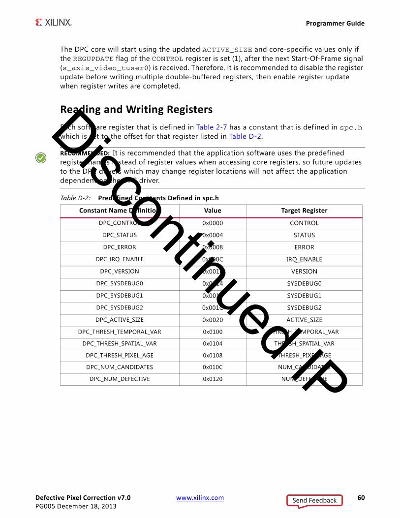
Defective Pixel Correction v7.0 www.xilinx.com 60PG005 December 18, 2013
Programmer Guide
The DPC core will start using the updated ACTIVE_SIZE and core-specific values only if the REGUPDATE flag of the CONTROL register is set (1), after the next Start-Of-Frame signal (s_axis_video_tuser0) is received. Therefore, it is recommended to disable the register update before writing multiple double-buffered registers, then enable register update when register writes are completed.
Reading and Writing RegistersEach software register that is defined in Table 2-7 has a constant that is defined in spc.h which is set to the offset for that register listed in Table D-2.
RECOMMENDED: It is recommended that the application software uses the predefined register names instead of register values when accessing core registers, so future updates to the DPC drivers which may change register locations will not affect the application dependent on the DPC driver.
Table D-2: Predefined Constants Defined in spc.h
Constant Name Definition Value Target Register
DPC_CONTROL 0x0000 CONTROL
DPC_STATUS 0x0004 STATUS
DPC_ERROR 0x0008 ERROR
DPC_IRQ_ENABLE 0x000C IRQ_ENABLE
DPC_VERSION 0x0010 VERSION
DPC_SYSDEBUG0 0x0014 SYSDEBUG0
DPC_SYSDEBUG1 0x0018 SYSDEBUG1
DPC_SYSDEBUG2 0x001C SYSDEBUG2
DPC_ACTIVE_SIZE 0x0020 ACTIVE_SIZE
DPC_THRESH_TEMPORAL_VAR 0x0100 THRESH_TEMPORAL_VAR
DPC_THRESH_SPATIAL_VAR 0x0104 THRESH_SPATIAL_VAR
DPC_THRESH_PIXEL_AGE 0x0108 THRESH_PIXEL_AGE
DPC_NUM_CANDIDATES 0x010C NUM_CANDIDATES
DPC_NUM_DEFECTIVE 0x0120 NUM_DEFECTIVE
Send Feedback
Discontinued IP

Defective Pixel Correction v7.0 www.xilinx.com 61PG005 December 18, 2013
Appendix E
Additional Resources
Xilinx ResourcesFor support resources such as Answers, Documentation, Downloads, and Forums, see the Xilinx Support website at:
http://www.xilinx.com/support.
For a glossary of technical terms used in Xilinx documentation, see:
http://www.xilinx.com/support/documentation/sw_manuals/glossary.pdf.
For a comprehensive listing of Video and Imaging application notes, white papers, reference designs and related IP cores, see the Video and Imaging Resources page at:
http://www.xilinx.com/esp/video/refdes_listing.htm#ref_des.
ReferencesThese documents provide supplemental material useful with this user guide:
1. AXI Reference Guide (UG761)
2. ISE to Vivado Design Suite Migration Guide (UG911)
3. Vivado Design Suite User Guide: Designing with IP (UG896)
4. Vivado Design Suite User Guide: Programming and Debugging (UG908)
5. Vivado Design Suite User Guide: Getting Started (UG910)
6. Vivado Design Suite User Guide: Logic Simulation (UG900)
7. Vivado Design Suite User Guide: Designing IP Subsystems Using IP Integrator (UG994)
Send Feedback
Discontinued IP

Defective Pixel Correction v7.0 www.xilinx.com 62PG005 December 18, 2013
Revision History
Revision HistoryThe following table shows the revision history for this document.
Notice of DisclaimerThe information disclosed to you hereunder (the “Materials”) is provided solely for the selection and use of Xilinx products. To the maximum extent permitted by applicable law: (1) Materials are made available “AS IS” and with all faults, Xilinx hereby DISCLAIMS ALL WARRANTIES AND CONDITIONS, EXPRESS, IMPLIED, OR STATUTORY, INCLUDING BUT NOT LIMITED TO WARRANTIES OF MERCHANTABILITY, NON-INFRINGEMENT, OR FITNESS FOR ANY PARTICULAR PURPOSE; and (2) Xilinx shall not be liable (whether in contract or tort, including negligence, or under any other theory of liability) for any loss or damage of any kind or nature related to, arising under, or in connection with, the Materials (including your use of the Materials), including for any direct, indirect, special, incidental, or consequential loss or damage (including loss of data, profits, goodwill, or any type of loss or damage suffered as a result of any action brought by a third party) even if such damage or loss was reasonably foreseeable or Xilinx had been advised of the possibility of the same. Xilinx assumes no obligation to correct any errors contained in the Materials or to notify you of updates to the Materials or to product specifications. You may not reproduce, modify, distribute, or publicly display the Materials without prior written consent. Certain products are subject to the terms and conditions of the Limited Warranties which can be viewed at http://www.xilinx.com/warranty.htm; IP cores may be subject to warranty and support terms contained in a license issued to you by Xilinx. Xilinx products are not designed or intended to be fail-safe or for use in any application requiring fail-safe performance; you assume sole risk and liability for use of Xilinx products in Critical Applications: http://www.xilinx.com/warranty.htm#critapps.© Copyright 2011–2013 Xilinx, Inc. Xilinx, the Xilinx logo, Artix, ISE, Kintex, Spartan, Virtex, Zynq, and other designated brands included herein are trademarks of Xilinx in the United States and other countries. All other trademarks are the property of their respective owners.
Date Version Revision10/19/2011 1.0 Initial Xilinx release of Product Guide, replacing DS721 and UG838.
4/24/2012 2.0 Updated for core version. Added Zynq-7000 devices, added AXI4-Stream interfaces, deprecated GPP interface.
07/25/2012 3.0 Updated for core version. Added Vivado information.
10/16/2012 3.1 Updated for core version. Added Vivado test bench.
03/20/2013 3.2 Updated for core version. Removed ISE chapters.
10/02/2013 7.0 Synch document version with core version. Updated Test Bench chapter and Debugging and Migration appendixes.
12/18/2013 7.0 Added UltraScale Architecture support.
Send Feedback
Discontinued IP